US9893004B2 - Semiconductor interposer integration - Google Patents
Semiconductor interposer integration Download PDFInfo
- Publication number
- US9893004B2 US9893004B2 US14/717,798 US201514717798A US9893004B2 US 9893004 B2 US9893004 B2 US 9893004B2 US 201514717798 A US201514717798 A US 201514717798A US 9893004 B2 US9893004 B2 US 9893004B2
- Authority
- US
- United States
- Prior art keywords
- semiconductor
- interposer
- semiconductor interposer
- interposers
- integrated circuit
- Prior art date
- Legal status (The legal status is an assumption and is not a legal conclusion. Google has not performed a legal analysis and makes no representation as to the accuracy of the status listed.)
- Active
Links
Images


Classifications
-
- H—ELECTRICITY
- H01—ELECTRIC ELEMENTS
- H01L—SEMICONDUCTOR DEVICES NOT COVERED BY CLASS H10
- H01L23/00—Details of semiconductor or other solid state devices
- H01L23/48—Arrangements for conducting electric current to or from the solid state body in operation, e.g. leads, terminal arrangements ; Selection of materials therefor
- H01L23/488—Arrangements for conducting electric current to or from the solid state body in operation, e.g. leads, terminal arrangements ; Selection of materials therefor consisting of soldered or bonded constructions
- H01L23/498—Leads, i.e. metallisations or lead-frames on insulating substrates, e.g. chip carriers
- H01L23/49827—Via connections through the substrates, e.g. pins going through the substrate, coaxial cables
-
- H—ELECTRICITY
- H01—ELECTRIC ELEMENTS
- H01L—SEMICONDUCTOR DEVICES NOT COVERED BY CLASS H10
- H01L21/00—Processes or apparatus adapted for the manufacture or treatment of semiconductor or solid state devices or of parts thereof
- H01L21/02—Manufacture or treatment of semiconductor devices or of parts thereof
- H01L21/04—Manufacture or treatment of semiconductor devices or of parts thereof the devices having potential barriers, e.g. a PN junction, depletion layer or carrier concentration layer
- H01L21/48—Manufacture or treatment of parts, e.g. containers, prior to assembly of the devices, using processes not provided for in a single one of the groups H01L21/18 - H01L21/326 or H10D48/04 - H10D48/07
- H01L21/4814—Conductive parts
- H01L21/4846—Leads on or in insulating or insulated substrates, e.g. metallisation
- H01L21/486—Via connections through the substrate with or without pins
-
- H—ELECTRICITY
- H01—ELECTRIC ELEMENTS
- H01L—SEMICONDUCTOR DEVICES NOT COVERED BY CLASS H10
- H01L21/00—Processes or apparatus adapted for the manufacture or treatment of semiconductor or solid state devices or of parts thereof
- H01L21/02—Manufacture or treatment of semiconductor devices or of parts thereof
- H01L21/04—Manufacture or treatment of semiconductor devices or of parts thereof the devices having potential barriers, e.g. a PN junction, depletion layer or carrier concentration layer
- H01L21/50—Assembly of semiconductor devices using processes or apparatus not provided for in a single one of the groups H01L21/18 - H01L21/326 or H10D48/04 - H10D48/07 e.g. sealing of a cap to a base of a container
- H01L21/52—Mounting semiconductor bodies in containers
-
- H—ELECTRICITY
- H01—ELECTRIC ELEMENTS
- H01L—SEMICONDUCTOR DEVICES NOT COVERED BY CLASS H10
- H01L23/00—Details of semiconductor or other solid state devices
- H01L23/02—Containers; Seals
- H01L23/04—Containers; Seals characterised by the shape of the container or parts, e.g. caps, walls
-
- H—ELECTRICITY
- H01—ELECTRIC ELEMENTS
- H01L—SEMICONDUCTOR DEVICES NOT COVERED BY CLASS H10
- H01L23/00—Details of semiconductor or other solid state devices
- H01L23/28—Encapsulations, e.g. encapsulating layers, coatings, e.g. for protection
- H01L23/31—Encapsulations, e.g. encapsulating layers, coatings, e.g. for protection characterised by the arrangement or shape
- H01L23/3107—Encapsulations, e.g. encapsulating layers, coatings, e.g. for protection characterised by the arrangement or shape the device being completely enclosed
-
- H—ELECTRICITY
- H01—ELECTRIC ELEMENTS
- H01L—SEMICONDUCTOR DEVICES NOT COVERED BY CLASS H10
- H01L23/00—Details of semiconductor or other solid state devices
- H01L23/34—Arrangements for cooling, heating, ventilating or temperature compensation ; Temperature sensing arrangements
- H01L23/46—Arrangements for cooling, heating, ventilating or temperature compensation ; Temperature sensing arrangements involving the transfer of heat by flowing fluids
- H01L23/473—Arrangements for cooling, heating, ventilating or temperature compensation ; Temperature sensing arrangements involving the transfer of heat by flowing fluids by flowing liquids
-
- H—ELECTRICITY
- H01—ELECTRIC ELEMENTS
- H01L—SEMICONDUCTOR DEVICES NOT COVERED BY CLASS H10
- H01L23/00—Details of semiconductor or other solid state devices
- H01L23/48—Arrangements for conducting electric current to or from the solid state body in operation, e.g. leads, terminal arrangements ; Selection of materials therefor
- H01L23/488—Arrangements for conducting electric current to or from the solid state body in operation, e.g. leads, terminal arrangements ; Selection of materials therefor consisting of soldered or bonded constructions
- H01L23/498—Leads, i.e. metallisations or lead-frames on insulating substrates, e.g. chip carriers
- H01L23/49833—Leads, i.e. metallisations or lead-frames on insulating substrates, e.g. chip carriers the chip support structure consisting of a plurality of insulating substrates
-
- H—ELECTRICITY
- H01—ELECTRIC ELEMENTS
- H01L—SEMICONDUCTOR DEVICES NOT COVERED BY CLASS H10
- H01L23/00—Details of semiconductor or other solid state devices
- H01L23/48—Arrangements for conducting electric current to or from the solid state body in operation, e.g. leads, terminal arrangements ; Selection of materials therefor
- H01L23/488—Arrangements for conducting electric current to or from the solid state body in operation, e.g. leads, terminal arrangements ; Selection of materials therefor consisting of soldered or bonded constructions
- H01L23/498—Leads, i.e. metallisations or lead-frames on insulating substrates, e.g. chip carriers
- H01L23/49838—Geometry or layout
-
- H—ELECTRICITY
- H01—ELECTRIC ELEMENTS
- H01L—SEMICONDUCTOR DEVICES NOT COVERED BY CLASS H10
- H01L23/00—Details of semiconductor or other solid state devices
- H01L23/57—Protection from inspection, reverse engineering or tampering
- H01L23/573—Protection from inspection, reverse engineering or tampering using passive means
-
- H—ELECTRICITY
- H01—ELECTRIC ELEMENTS
- H01L—SEMICONDUCTOR DEVICES NOT COVERED BY CLASS H10
- H01L23/00—Details of semiconductor or other solid state devices
- H01L23/58—Structural electrical arrangements for semiconductor devices not otherwise provided for, e.g. in combination with batteries
- H01L23/64—Impedance arrangements
- H01L23/66—High-frequency adaptations
-
- H—ELECTRICITY
- H01—ELECTRIC ELEMENTS
- H01L—SEMICONDUCTOR DEVICES NOT COVERED BY CLASS H10
- H01L25/00—Assemblies consisting of a plurality of semiconductor or other solid state devices
- H01L25/03—Assemblies consisting of a plurality of semiconductor or other solid state devices all the devices being of a type provided for in a single subclass of subclasses H10B, H10D, H10F, H10H, H10K or H10N, e.g. assemblies of rectifier diodes
- H01L25/04—Assemblies consisting of a plurality of semiconductor or other solid state devices all the devices being of a type provided for in a single subclass of subclasses H10B, H10D, H10F, H10H, H10K or H10N, e.g. assemblies of rectifier diodes the devices not having separate containers
- H01L25/065—Assemblies consisting of a plurality of semiconductor or other solid state devices all the devices being of a type provided for in a single subclass of subclasses H10B, H10D, H10F, H10H, H10K or H10N, e.g. assemblies of rectifier diodes the devices not having separate containers the devices being of a type provided for in group H10D89/00
- H01L25/0652—Assemblies consisting of a plurality of semiconductor or other solid state devices all the devices being of a type provided for in a single subclass of subclasses H10B, H10D, H10F, H10H, H10K or H10N, e.g. assemblies of rectifier diodes the devices not having separate containers the devices being of a type provided for in group H10D89/00 the devices being arranged next and on each other, i.e. mixed assemblies
-
- H—ELECTRICITY
- H01—ELECTRIC ELEMENTS
- H01L—SEMICONDUCTOR DEVICES NOT COVERED BY CLASS H10
- H01L25/00—Assemblies consisting of a plurality of semiconductor or other solid state devices
- H01L25/03—Assemblies consisting of a plurality of semiconductor or other solid state devices all the devices being of a type provided for in a single subclass of subclasses H10B, H10D, H10F, H10H, H10K or H10N, e.g. assemblies of rectifier diodes
- H01L25/04—Assemblies consisting of a plurality of semiconductor or other solid state devices all the devices being of a type provided for in a single subclass of subclasses H10B, H10D, H10F, H10H, H10K or H10N, e.g. assemblies of rectifier diodes the devices not having separate containers
- H01L25/065—Assemblies consisting of a plurality of semiconductor or other solid state devices all the devices being of a type provided for in a single subclass of subclasses H10B, H10D, H10F, H10H, H10K or H10N, e.g. assemblies of rectifier diodes the devices not having separate containers the devices being of a type provided for in group H10D89/00
- H01L25/0657—Stacked arrangements of devices
-
- H—ELECTRICITY
- H01—ELECTRIC ELEMENTS
- H01L—SEMICONDUCTOR DEVICES NOT COVERED BY CLASS H10
- H01L25/00—Assemblies consisting of a plurality of semiconductor or other solid state devices
- H01L25/18—Assemblies consisting of a plurality of semiconductor or other solid state devices the devices being of the types provided for in two or more different main groups of the same subclass of H10B, H10D, H10F, H10H, H10K or H10N
-
- H—ELECTRICITY
- H01—ELECTRIC ELEMENTS
- H01L—SEMICONDUCTOR DEVICES NOT COVERED BY CLASS H10
- H01L25/00—Assemblies consisting of a plurality of semiconductor or other solid state devices
- H01L25/50—Multistep manufacturing processes of assemblies consisting of devices, the devices being individual devices of subclass H10D or integrated devices of class H10
-
- H10W20/20—
-
- H10W40/47—
-
- H10W42/40—
-
- H10W44/20—
-
- H10W70/095—
-
- H10W70/635—
-
- H10W70/65—
-
- H10W70/698—
-
- H10W72/071—
-
- H10W74/111—
-
- H10W76/12—
-
- H10W90/00—
-
- H10W90/293—
-
- H10W90/401—
-
- H—ELECTRICITY
- H01—ELECTRIC ELEMENTS
- H01L—SEMICONDUCTOR DEVICES NOT COVERED BY CLASS H10
- H01L2224/00—Indexing scheme for arrangements for connecting or disconnecting semiconductor or solid-state bodies and methods related thereto as covered by H01L24/00
- H01L2224/01—Means for bonding being attached to, or being formed on, the surface to be connected, e.g. chip-to-package, die-attach, "first-level" interconnects; Manufacturing methods related thereto
- H01L2224/42—Wire connectors; Manufacturing methods related thereto
- H01L2224/44—Structure, shape, material or disposition of the wire connectors prior to the connecting process
- H01L2224/45—Structure, shape, material or disposition of the wire connectors prior to the connecting process of an individual wire connector
- H01L2224/45001—Core members of the connector
- H01L2224/4501—Shape
- H01L2224/45012—Cross-sectional shape
- H01L2224/45015—Cross-sectional shape being circular
-
- H—ELECTRICITY
- H01—ELECTRIC ELEMENTS
- H01L—SEMICONDUCTOR DEVICES NOT COVERED BY CLASS H10
- H01L2224/00—Indexing scheme for arrangements for connecting or disconnecting semiconductor or solid-state bodies and methods related thereto as covered by H01L24/00
- H01L2224/01—Means for bonding being attached to, or being formed on, the surface to be connected, e.g. chip-to-package, die-attach, "first-level" interconnects; Manufacturing methods related thereto
- H01L2224/42—Wire connectors; Manufacturing methods related thereto
- H01L2224/44—Structure, shape, material or disposition of the wire connectors prior to the connecting process
- H01L2224/45—Structure, shape, material or disposition of the wire connectors prior to the connecting process of an individual wire connector
- H01L2224/45001—Core members of the connector
- H01L2224/45099—Material
-
- H—ELECTRICITY
- H01—ELECTRIC ELEMENTS
- H01L—SEMICONDUCTOR DEVICES NOT COVERED BY CLASS H10
- H01L2224/00—Indexing scheme for arrangements for connecting or disconnecting semiconductor or solid-state bodies and methods related thereto as covered by H01L24/00
- H01L2224/01—Means for bonding being attached to, or being formed on, the surface to be connected, e.g. chip-to-package, die-attach, "first-level" interconnects; Manufacturing methods related thereto
- H01L2224/42—Wire connectors; Manufacturing methods related thereto
- H01L2224/47—Structure, shape, material or disposition of the wire connectors after the connecting process
- H01L2224/48—Structure, shape, material or disposition of the wire connectors after the connecting process of an individual wire connector
- H01L2224/481—Disposition
- H01L2224/48151—Connecting between a semiconductor or solid-state body and an item not being a semiconductor or solid-state body, e.g. chip-to-substrate, chip-to-passive
- H01L2224/48221—Connecting between a semiconductor or solid-state body and an item not being a semiconductor or solid-state body, e.g. chip-to-substrate, chip-to-passive the body and the item being stacked
- H01L2224/48225—Connecting between a semiconductor or solid-state body and an item not being a semiconductor or solid-state body, e.g. chip-to-substrate, chip-to-passive the body and the item being stacked the item being non-metallic, e.g. insulating substrate with or without metallisation
- H01L2224/48227—Connecting between a semiconductor or solid-state body and an item not being a semiconductor or solid-state body, e.g. chip-to-substrate, chip-to-passive the body and the item being stacked the item being non-metallic, e.g. insulating substrate with or without metallisation connecting the wire to a bond pad of the item
-
- H—ELECTRICITY
- H01—ELECTRIC ELEMENTS
- H01L—SEMICONDUCTOR DEVICES NOT COVERED BY CLASS H10
- H01L2225/00—Details relating to assemblies covered by the group H01L25/00 but not provided for in its subgroups
- H01L2225/03—All the devices being of a type provided for in the same main group of the same subclass of class H10, e.g. assemblies of rectifier diodes
- H01L2225/04—All the devices being of a type provided for in the same main group of the same subclass of class H10, e.g. assemblies of rectifier diodes the devices not having separate containers
- H01L2225/065—All the devices being of a type provided for in the same main group of the same subclass of class H10
- H01L2225/06503—Stacked arrangements of devices
- H01L2225/06513—Bump or bump-like direct electrical connections between devices, e.g. flip-chip connection, solder bumps
-
- H—ELECTRICITY
- H01—ELECTRIC ELEMENTS
- H01L—SEMICONDUCTOR DEVICES NOT COVERED BY CLASS H10
- H01L2225/00—Details relating to assemblies covered by the group H01L25/00 but not provided for in its subgroups
- H01L2225/03—All the devices being of a type provided for in the same main group of the same subclass of class H10, e.g. assemblies of rectifier diodes
- H01L2225/04—All the devices being of a type provided for in the same main group of the same subclass of class H10, e.g. assemblies of rectifier diodes the devices not having separate containers
- H01L2225/065—All the devices being of a type provided for in the same main group of the same subclass of class H10
- H01L2225/06503—Stacked arrangements of devices
- H01L2225/06517—Bump or bump-like direct electrical connections from device to substrate
-
- H—ELECTRICITY
- H01—ELECTRIC ELEMENTS
- H01L—SEMICONDUCTOR DEVICES NOT COVERED BY CLASS H10
- H01L2225/00—Details relating to assemblies covered by the group H01L25/00 but not provided for in its subgroups
- H01L2225/03—All the devices being of a type provided for in the same main group of the same subclass of class H10, e.g. assemblies of rectifier diodes
- H01L2225/04—All the devices being of a type provided for in the same main group of the same subclass of class H10, e.g. assemblies of rectifier diodes the devices not having separate containers
- H01L2225/065—All the devices being of a type provided for in the same main group of the same subclass of class H10
- H01L2225/06503—Stacked arrangements of devices
- H01L2225/06527—Special adaptation of electrical connections, e.g. rewiring, engineering changes, pressure contacts, layout
-
- H—ELECTRICITY
- H01—ELECTRIC ELEMENTS
- H01L—SEMICONDUCTOR DEVICES NOT COVERED BY CLASS H10
- H01L2225/00—Details relating to assemblies covered by the group H01L25/00 but not provided for in its subgroups
- H01L2225/03—All the devices being of a type provided for in the same main group of the same subclass of class H10, e.g. assemblies of rectifier diodes
- H01L2225/04—All the devices being of a type provided for in the same main group of the same subclass of class H10, e.g. assemblies of rectifier diodes the devices not having separate containers
- H01L2225/065—All the devices being of a type provided for in the same main group of the same subclass of class H10
- H01L2225/06503—Stacked arrangements of devices
- H01L2225/06541—Conductive via connections through the device, e.g. vertical interconnects, through silicon via [TSV]
-
- H—ELECTRICITY
- H01—ELECTRIC ELEMENTS
- H01L—SEMICONDUCTOR DEVICES NOT COVERED BY CLASS H10
- H01L2225/00—Details relating to assemblies covered by the group H01L25/00 but not provided for in its subgroups
- H01L2225/03—All the devices being of a type provided for in the same main group of the same subclass of class H10, e.g. assemblies of rectifier diodes
- H01L2225/04—All the devices being of a type provided for in the same main group of the same subclass of class H10, e.g. assemblies of rectifier diodes the devices not having separate containers
- H01L2225/065—All the devices being of a type provided for in the same main group of the same subclass of class H10
- H01L2225/06503—Stacked arrangements of devices
- H01L2225/06548—Conductive via connections through the substrate, container, or encapsulation
-
- H—ELECTRICITY
- H01—ELECTRIC ELEMENTS
- H01L—SEMICONDUCTOR DEVICES NOT COVERED BY CLASS H10
- H01L2225/00—Details relating to assemblies covered by the group H01L25/00 but not provided for in its subgroups
- H01L2225/03—All the devices being of a type provided for in the same main group of the same subclass of class H10, e.g. assemblies of rectifier diodes
- H01L2225/04—All the devices being of a type provided for in the same main group of the same subclass of class H10, e.g. assemblies of rectifier diodes the devices not having separate containers
- H01L2225/065—All the devices being of a type provided for in the same main group of the same subclass of class H10
- H01L2225/06503—Stacked arrangements of devices
- H01L2225/06572—Auxiliary carrier between devices, the carrier having an electrical connection structure
-
- H—ELECTRICITY
- H01—ELECTRIC ELEMENTS
- H01L—SEMICONDUCTOR DEVICES NOT COVERED BY CLASS H10
- H01L24/00—Arrangements for connecting or disconnecting semiconductor or solid-state bodies; Methods or apparatus related thereto
- H01L24/01—Means for bonding being attached to, or being formed on, the surface to be connected, e.g. chip-to-package, die-attach, "first-level" interconnects; Manufacturing methods related thereto
- H01L24/42—Wire connectors; Manufacturing methods related thereto
- H01L24/47—Structure, shape, material or disposition of the wire connectors after the connecting process
- H01L24/48—Structure, shape, material or disposition of the wire connectors after the connecting process of an individual wire connector
-
- H—ELECTRICITY
- H01—ELECTRIC ELEMENTS
- H01L—SEMICONDUCTOR DEVICES NOT COVERED BY CLASS H10
- H01L2924/00—Indexing scheme for arrangements or methods for connecting or disconnecting semiconductor or solid-state bodies as covered by H01L24/00
-
- H—ELECTRICITY
- H01—ELECTRIC ELEMENTS
- H01L—SEMICONDUCTOR DEVICES NOT COVERED BY CLASS H10
- H01L2924/00—Indexing scheme for arrangements or methods for connecting or disconnecting semiconductor or solid-state bodies as covered by H01L24/00
- H01L2924/0001—Technical content checked by a classifier
- H01L2924/00014—Technical content checked by a classifier the subject-matter covered by the group, the symbol of which is combined with the symbol of this group, being disclosed without further technical details
-
- H—ELECTRICITY
- H01—ELECTRIC ELEMENTS
- H01L—SEMICONDUCTOR DEVICES NOT COVERED BY CLASS H10
- H01L2924/00—Indexing scheme for arrangements or methods for connecting or disconnecting semiconductor or solid-state bodies as covered by H01L24/00
- H01L2924/10—Details of semiconductor or other solid state devices to be connected
- H01L2924/102—Material of the semiconductor or solid state bodies
- H01L2924/1025—Semiconducting materials
- H01L2924/10251—Elemental semiconductors, i.e. Group IV
- H01L2924/10253—Silicon [Si]
-
- H—ELECTRICITY
- H01—ELECTRIC ELEMENTS
- H01L—SEMICONDUCTOR DEVICES NOT COVERED BY CLASS H10
- H01L2924/00—Indexing scheme for arrangements or methods for connecting or disconnecting semiconductor or solid-state bodies as covered by H01L24/00
- H01L2924/19—Details of hybrid assemblies other than the semiconductor or other solid state devices to be connected
- H01L2924/1901—Structure
- H01L2924/1904—Component type
- H01L2924/19041—Component type being a capacitor
-
- H—ELECTRICITY
- H01—ELECTRIC ELEMENTS
- H01L—SEMICONDUCTOR DEVICES NOT COVERED BY CLASS H10
- H01L2924/00—Indexing scheme for arrangements or methods for connecting or disconnecting semiconductor or solid-state bodies as covered by H01L24/00
- H01L2924/20—Parameters
- H01L2924/207—Diameter ranges
-
- H—ELECTRICITY
- H01—ELECTRIC ELEMENTS
- H01L—SEMICONDUCTOR DEVICES NOT COVERED BY CLASS H10
- H01L2924/00—Indexing scheme for arrangements or methods for connecting or disconnecting semiconductor or solid-state bodies as covered by H01L24/00
- H01L2924/30—Technical effects
- H01L2924/301—Electrical effects
- H01L2924/30107—Inductance
-
- H10W72/01—
-
- H10W72/252—
-
- H10W72/823—
-
- H10W72/884—
-
- H10W74/00—
-
- H10W90/22—
-
- H10W90/297—
-
- H10W90/701—
-
- H10W90/722—
-
- H10W90/724—
-
- H10W90/732—
-
- H10W90/754—
-
- Y—GENERAL TAGGING OF NEW TECHNOLOGICAL DEVELOPMENTS; GENERAL TAGGING OF CROSS-SECTIONAL TECHNOLOGIES SPANNING OVER SEVERAL SECTIONS OF THE IPC; TECHNICAL SUBJECTS COVERED BY FORMER USPC CROSS-REFERENCE ART COLLECTIONS [XRACs] AND DIGESTS
- Y10—TECHNICAL SUBJECTS COVERED BY FORMER USPC
- Y10T—TECHNICAL SUBJECTS COVERED BY FORMER US CLASSIFICATION
- Y10T29/00—Metal working
- Y10T29/53—Means to assemble or disassemble
- Y10T29/5313—Means to assemble electrical device
- Y10T29/53174—Means to fasten electrical component to wiring board, base, or substrate
- Y10T29/53178—Chip component
-
- Y—GENERAL TAGGING OF NEW TECHNOLOGICAL DEVELOPMENTS; GENERAL TAGGING OF CROSS-SECTIONAL TECHNOLOGIES SPANNING OVER SEVERAL SECTIONS OF THE IPC; TECHNICAL SUBJECTS COVERED BY FORMER USPC CROSS-REFERENCE ART COLLECTIONS [XRACs] AND DIGESTS
- Y10—TECHNICAL SUBJECTS COVERED BY FORMER USPC
- Y10T—TECHNICAL SUBJECTS COVERED BY FORMER US CLASSIFICATION
- Y10T29/00—Metal working
- Y10T29/53—Means to assemble or disassemble
- Y10T29/5313—Means to assemble electrical device
- Y10T29/53174—Means to fasten electrical component to wiring board, base, or substrate
- Y10T29/53183—Multilead component
Definitions
- Embodiments disclosed herein pertain to electronic packages including a first semiconductor interposer.
- the first semiconductor interposer includes a first plurality of through substrate vias perpendicular to the major plane of the first semiconductor interposer and passing through the entire thickness of the first semiconductor interposer.
- the embodiments further include a second semiconductor interposer electrically coupled to the first semiconductor interposer by a second plurality of electrical connections.
- the embodiments further include a third semiconductor interposer electrically coupled to the second semiconductor interposer.
- the embodiments further include a top semiconductor interposer electrically coupled to the third semiconductor interposer.
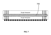
- FIG. 7 is a schematic of a stack of interposers using an oxide layer for rigidity according to embodiments.
- Top and Up will be used herein to describe portions/directions perpendicularly distal from the printed circuit board (PCB) plane and further away from the center of mass of the PCB in the perpendicular direction.
- Vertical will be used to describe items aligned in the “Up” direction towards the “Top”. Other similar terms may be used whose meanings will now be clear.
Landscapes
- Engineering & Computer Science (AREA)
- Microelectronics & Electronic Packaging (AREA)
- Power Engineering (AREA)
- Physics & Mathematics (AREA)
- Condensed Matter Physics & Semiconductors (AREA)
- General Physics & Mathematics (AREA)
- Computer Hardware Design (AREA)
- Manufacturing & Machinery (AREA)
- Semiconductor Integrated Circuits (AREA)
- Ceramic Engineering (AREA)
- Geometry (AREA)
- Wire Bonding (AREA)
Abstract
Description
Claims (14)
Priority Applications (14)
| Application Number | Priority Date | Filing Date | Title |
|---|---|---|---|
| US14/717,798 US9893004B2 (en) | 2011-07-27 | 2015-05-20 | Semiconductor interposer integration |
| US14/746,045 US9818680B2 (en) | 2011-07-27 | 2015-06-22 | Scalable semiconductor interposer integration |
| US15/164,866 US10026720B2 (en) | 2015-05-20 | 2016-05-25 | Semiconductor structure and a method of making thereof |
| US15/810,050 US10515886B2 (en) | 2008-09-06 | 2017-11-11 | Scalable semiconductor interposer integration |
| US16/035,623 US10964676B2 (en) | 2008-09-06 | 2018-07-14 | Semiconductor structure and a method of making thereof |
| US16/724,319 US11302617B2 (en) | 2008-09-06 | 2019-12-22 | Scalable semiconductor interposer integration |
| US17/180,835 US20210175162A1 (en) | 2011-07-27 | 2021-02-21 | Secure semiconductor integration |
| US17/196,721 US11569208B2 (en) | 2015-05-20 | 2021-03-09 | Semiconductor structure and method for making thereof |
| US17/229,866 US12255189B2 (en) | 2015-05-20 | 2021-04-14 | Secure semiconductor integration and method for making thereof |
| US17/688,747 US12068231B2 (en) | 2014-05-24 | 2022-03-07 | 3D integrations and methods of making thereof |
| US17/959,373 US20230026177A1 (en) | 2015-05-20 | 2022-10-04 | Enhanced semiconductor structures |
| US17/966,946 US20230041977A1 (en) | 2015-05-20 | 2022-10-17 | 3d heterogeneous integrations and methods of making thereof |
| US18/396,884 US12327783B2 (en) | 2011-07-27 | 2023-12-27 | 3D system integration |
| US18/761,561 US20240355722A1 (en) | 2014-05-24 | 2024-07-02 | Apparatus and method for making a secured substrate |
Applications Claiming Priority (3)
| Application Number | Priority Date | Filing Date | Title |
|---|---|---|---|
| US13/192,217 US10236275B2 (en) | 2008-09-06 | 2011-07-27 | Stacking integrated circuits containing serializer and deserializer blocks using through silicon via |
| US201462002794P | 2014-05-24 | 2014-05-24 | |
| US14/717,798 US9893004B2 (en) | 2011-07-27 | 2015-05-20 | Semiconductor interposer integration |
Related Parent Applications (3)
| Application Number | Title | Priority Date | Filing Date |
|---|---|---|---|
| US13/192,217 Continuation-In-Part US10236275B2 (en) | 2008-09-06 | 2011-07-27 | Stacking integrated circuits containing serializer and deserializer blocks using through silicon via |
| US13/192,217 Continuation US10236275B2 (en) | 2008-09-06 | 2011-07-27 | Stacking integrated circuits containing serializer and deserializer blocks using through silicon via |
| US14/746,045 Continuation-In-Part US9818680B2 (en) | 2008-09-06 | 2015-06-22 | Scalable semiconductor interposer integration |
Related Child Applications (4)
| Application Number | Title | Priority Date | Filing Date |
|---|---|---|---|
| US14/746,045 Continuation-In-Part US9818680B2 (en) | 2008-09-06 | 2015-06-22 | Scalable semiconductor interposer integration |
| US14/746,045 Continuation US9818680B2 (en) | 2008-09-06 | 2015-06-22 | Scalable semiconductor interposer integration |
| US15/164,866 Continuation-In-Part US10026720B2 (en) | 2008-09-06 | 2016-05-25 | Semiconductor structure and a method of making thereof |
| US15/810,050 Continuation-In-Part US10515886B2 (en) | 2008-09-06 | 2017-11-11 | Scalable semiconductor interposer integration |
Publications (2)
| Publication Number | Publication Date |
|---|---|
| US20150255434A1 US20150255434A1 (en) | 2015-09-10 |
| US9893004B2 true US9893004B2 (en) | 2018-02-13 |
Family
ID=54018130
Family Applications (2)
| Application Number | Title | Priority Date | Filing Date |
|---|---|---|---|
| US14/717,798 Active US9893004B2 (en) | 2008-09-06 | 2015-05-20 | Semiconductor interposer integration |
| US18/396,884 Active US12327783B2 (en) | 2008-09-06 | 2023-12-27 | 3D system integration |
Family Applications After (1)
| Application Number | Title | Priority Date | Filing Date |
|---|---|---|---|
| US18/396,884 Active US12327783B2 (en) | 2008-09-06 | 2023-12-27 | 3D system integration |
Country Status (1)
| Country | Link |
|---|---|
| US (2) | US9893004B2 (en) |
Cited By (104)
| Publication number | Priority date | Publication date | Assignee | Title |
|---|---|---|---|---|
| US20180277495A1 (en) * | 2013-08-16 | 2018-09-27 | Taiwan Semiconductor Manufacturing Company, Ltd. | Packages with Interposers and Methods for Forming the Same |
| US10508030B2 (en) | 2017-03-21 | 2019-12-17 | Invensas Bonding Technologies, Inc. | Seal for microelectronic assembly |
| US10515913B2 (en) | 2017-03-17 | 2019-12-24 | Invensas Bonding Technologies, Inc. | Multi-metal contact structure |
| US10515925B2 (en) | 2017-04-21 | 2019-12-24 | Invensas Bonding Technologies, Inc. | Die processing |
| US10522499B2 (en) | 2017-02-09 | 2019-12-31 | Invensas Bonding Technologies, Inc. | Bonded structures |
| US10529634B2 (en) | 2017-05-11 | 2020-01-07 | Invensas Bonding Technologies, Inc. | Probe methodology for ultrafine pitch interconnects |
| US10546832B2 (en) | 2016-12-21 | 2020-01-28 | Invensas Bonding Technologies, Inc. | Bonded structures |
| US10607937B2 (en) | 2015-12-18 | 2020-03-31 | Invensas Bonding Technologies, Inc. | Increased contact alignment tolerance for direct bonding |
| US10658313B2 (en) | 2017-12-11 | 2020-05-19 | Invensas Bonding Technologies, Inc. | Selective recess |
| US10727219B2 (en) | 2018-02-15 | 2020-07-28 | Invensas Bonding Technologies, Inc. | Techniques for processing devices |
| US10777533B2 (en) | 2012-08-30 | 2020-09-15 | Invensas Bonding Technologies, Inc. | Heterogeneous device |
| US10784191B2 (en) | 2017-03-31 | 2020-09-22 | Invensas Bonding Technologies, Inc. | Interface structures and methods for forming same |
| US10790262B2 (en) | 2018-04-11 | 2020-09-29 | Invensas Bonding Technologies, Inc. | Low temperature bonded structures |
| US10796936B2 (en) | 2016-12-22 | 2020-10-06 | Invensas Bonding Technologies, Inc. | Die tray with channels |
| US10840205B2 (en) | 2017-09-24 | 2020-11-17 | Invensas Bonding Technologies, Inc. | Chemical mechanical polishing for hybrid bonding |
| US10879226B2 (en) | 2016-05-19 | 2020-12-29 | Invensas Bonding Technologies, Inc. | Stacked dies and methods for forming bonded structures |
| US10879212B2 (en) | 2017-05-11 | 2020-12-29 | Invensas Bonding Technologies, Inc. | Processed stacked dies |
| US10896902B2 (en) | 2016-01-13 | 2021-01-19 | Invensas Bonding Technologies, Inc. | Systems and methods for efficient transfer of semiconductor elements |
| US10923408B2 (en) | 2017-12-22 | 2021-02-16 | Invensas Bonding Technologies, Inc. | Cavity packages |
| US10964664B2 (en) | 2018-04-20 | 2021-03-30 | Invensas Bonding Technologies, Inc. | DBI to Si bonding for simplified handle wafer |
| US10998292B2 (en) | 2018-06-13 | 2021-05-04 | Invensas Bonding Technologies, Inc. | Offset pads over TSV |
| US10998265B2 (en) | 2016-09-30 | 2021-05-04 | Invensas Bonding Technologies, Inc. | Interface structures and methods for forming same |
| US11004757B2 (en) | 2018-05-14 | 2021-05-11 | Invensas Bonding Technologies, Inc. | Bonded structures |
| US11011503B2 (en) | 2017-12-15 | 2021-05-18 | Invensas Bonding Technologies, Inc. | Direct-bonded optoelectronic interconnect for high-density integrated photonics |
| US11011494B2 (en) | 2018-08-31 | 2021-05-18 | Invensas Bonding Technologies, Inc. | Layer structures for making direct metal-to-metal bonds at low temperatures in microelectronics |
| US11011418B2 (en) | 2005-08-11 | 2021-05-18 | Invensas Bonding Technologies, Inc. | 3D IC method and device |
| US11031285B2 (en) | 2017-10-06 | 2021-06-08 | Invensas Bonding Technologies, Inc. | Diffusion barrier collar for interconnects |
| US11056390B2 (en) | 2015-06-24 | 2021-07-06 | Invensas Corporation | Structures and methods for reliable packages |
| US11056348B2 (en) | 2018-04-05 | 2021-07-06 | Invensas Bonding Technologies, Inc. | Bonding surfaces for microelectronics |
| WO2021173204A1 (en) * | 2020-02-25 | 2021-09-02 | Tokyo Electron Limited | Split substrate interposer |
| US20210327851A1 (en) * | 2017-04-27 | 2021-10-21 | Invensas Corporation | Embedded organic interposer for high bandwidth |
| US11158573B2 (en) | 2018-10-22 | 2021-10-26 | Invensas Bonding Technologies, Inc. | Interconnect structures |
| US11158606B2 (en) | 2018-07-06 | 2021-10-26 | Invensas Bonding Technologies, Inc. | Molded direct bonded and interconnected stack |
| US11171117B2 (en) | 2018-06-12 | 2021-11-09 | Invensas Bonding Technologies, Inc. | Interlayer connection of stacked microelectronic components |
| US11169326B2 (en) | 2018-02-26 | 2021-11-09 | Invensas Bonding Technologies, Inc. | Integrated optical waveguides, direct-bonded waveguide interface joints, optical routing and interconnects |
| US11195748B2 (en) | 2017-09-27 | 2021-12-07 | Invensas Corporation | Interconnect structures and methods for forming same |
| US11195789B2 (en) * | 2018-11-30 | 2021-12-07 | International Business Machines Corporation | Integrated circuit module with a structurally balanced package using a bottom side interposer |
| US11205600B2 (en) | 2014-03-12 | 2021-12-21 | Invensas Corporation | Integrated circuits protected by substrates with cavities, and methods of manufacture |
| US11205625B2 (en) | 2019-04-12 | 2021-12-21 | Invensas Bonding Technologies, Inc. | Wafer-level bonding of obstructive elements |
| US11244916B2 (en) | 2018-04-11 | 2022-02-08 | Invensas Bonding Technologies, Inc. | Low temperature bonded structures |
| US11244920B2 (en) | 2018-12-18 | 2022-02-08 | Invensas Bonding Technologies, Inc. | Method and structures for low temperature device bonding |
| US11256004B2 (en) | 2018-03-20 | 2022-02-22 | Invensas Bonding Technologies, Inc. | Direct-bonded lamination for improved image clarity in optical devices |
| US11264345B2 (en) | 2015-08-25 | 2022-03-01 | Invensas Bonding Technologies, Inc. | Conductive barrier direct hybrid bonding |
| US11276676B2 (en) | 2018-05-15 | 2022-03-15 | Invensas Bonding Technologies, Inc. | Stacked devices and methods of fabrication |
| US11296053B2 (en) | 2019-06-26 | 2022-04-05 | Invensas Bonding Technologies, Inc. | Direct bonded stack structures for increased reliability and improved yield in microelectronics |
| US11296044B2 (en) | 2018-08-29 | 2022-04-05 | Invensas Bonding Technologies, Inc. | Bond enhancement structure in microelectronics for trapping contaminants during direct-bonding processes |
| US11348801B2 (en) | 2016-12-28 | 2022-05-31 | Invensas Bonding Technologies, Inc. | Processing stacked substrates |
| US11355404B2 (en) | 2019-04-22 | 2022-06-07 | Invensas Bonding Technologies, Inc. | Mitigating surface damage of probe pads in preparation for direct bonding of a substrate |
| US11367652B2 (en) | 2016-12-28 | 2022-06-21 | Invensas Bonding Technologies, Inc. | Microelectronic assembly from processed substrate |
| US11373963B2 (en) | 2019-04-12 | 2022-06-28 | Invensas Bonding Technologies, Inc. | Protective elements for bonded structures |
| US11380597B2 (en) | 2017-12-22 | 2022-07-05 | Invensas Bonding Technologies, Inc. | Bonded structures |
| US11387214B2 (en) | 2017-06-15 | 2022-07-12 | Invensas Llc | Multi-chip modules formed using wafer-level processing of a reconstituted wafer |
| US11385278B2 (en) | 2019-05-23 | 2022-07-12 | Invensas Bonding Technologies, Inc. | Security circuitry for bonded structures |
| US11393779B2 (en) | 2018-06-13 | 2022-07-19 | Invensas Bonding Technologies, Inc. | Large metal pads over TSV |
| US11462419B2 (en) | 2018-07-06 | 2022-10-04 | Invensas Bonding Technologies, Inc. | Microelectronic assemblies |
| US11476213B2 (en) | 2019-01-14 | 2022-10-18 | Invensas Bonding Technologies, Inc. | Bonded structures without intervening adhesive |
| US20220359463A1 (en) * | 2019-06-28 | 2022-11-10 | Taiwan Semiconductor Manufacturing Company, Ltd. | Package and manufacturing method thereof |
| US11515291B2 (en) | 2018-08-28 | 2022-11-29 | Adeia Semiconductor Inc. | Integrated voltage regulator and passive components |
| US11538781B2 (en) | 2020-06-30 | 2022-12-27 | Adeia Semiconductor Bonding Technologies Inc. | Integrated device packages including bonded structures |
| US11610846B2 (en) | 2019-04-12 | 2023-03-21 | Adeia Semiconductor Bonding Technologies Inc. | Protective elements for bonded structures including an obstructive element |
| US11621246B2 (en) | 2019-03-29 | 2023-04-04 | Adeia Semiconductor Technologies Llc | Diffused bitline replacement in stacked wafer memory |
| US11626363B2 (en) | 2016-12-29 | 2023-04-11 | Adeia Semiconductor Bonding Technologies Inc. | Bonded structures with integrated passive component |
| US11664357B2 (en) | 2018-07-03 | 2023-05-30 | Adeia Semiconductor Bonding Technologies Inc. | Techniques for joining dissimilar materials in microelectronics |
| US11710718B2 (en) | 2015-07-10 | 2023-07-25 | Adeia Semiconductor Technologies Llc | Structures and methods for low temperature bonding using nanoparticles |
| US11715730B2 (en) | 2017-03-16 | 2023-08-01 | Adeia Semiconductor Technologies Llc | Direct-bonded LED arrays including optical elements configured to transmit optical signals from LED elements |
| US11721653B2 (en) | 2019-12-23 | 2023-08-08 | Adeia Semiconductor Bonding Technologies Inc. | Circuitry for electrical redundancy in bonded structures |
| US11728273B2 (en) | 2020-09-04 | 2023-08-15 | Adeia Semiconductor Bonding Technologies Inc. | Bonded structure with interconnect structure |
| US11735523B2 (en) | 2020-05-19 | 2023-08-22 | Adeia Semiconductor Bonding Technologies Inc. | Laterally unconfined structure |
| US11742314B2 (en) | 2020-03-31 | 2023-08-29 | Adeia Semiconductor Bonding Technologies Inc. | Reliable hybrid bonded apparatus |
| US11762200B2 (en) | 2019-12-17 | 2023-09-19 | Adeia Semiconductor Bonding Technologies Inc. | Bonded optical devices |
| US11764177B2 (en) | 2020-09-04 | 2023-09-19 | Adeia Semiconductor Bonding Technologies Inc. | Bonded structure with interconnect structure |
| US11760059B2 (en) | 2003-05-19 | 2023-09-19 | Adeia Semiconductor Bonding Technologies Inc. | Method of room temperature covalent bonding |
| US11842894B2 (en) | 2019-12-23 | 2023-12-12 | Adeia Semiconductor Bonding Technologies Inc. | Electrical redundancy for bonded structures |
| US11862604B2 (en) | 2018-06-22 | 2024-01-02 | Adeia Semiconductor Inc. | Systems and methods for releveled bump planes for chiplets |
| US11862602B2 (en) | 2019-11-07 | 2024-01-02 | Adeia Semiconductor Technologies Llc | Scalable architecture for reduced cycles across SOC |
| US11876076B2 (en) | 2019-12-20 | 2024-01-16 | Adeia Semiconductor Technologies Llc | Apparatus for non-volatile random access memory stacks |
| US11881454B2 (en) | 2016-10-07 | 2024-01-23 | Adeia Semiconductor Inc. | Stacked IC structure with orthogonal interconnect layers |
| US11901281B2 (en) | 2019-03-11 | 2024-02-13 | Adeia Semiconductor Bonding Technologies Inc. | Bonded structures with integrated passive component |
| US11908739B2 (en) | 2017-06-05 | 2024-02-20 | Adeia Semiconductor Technologies Llc | Flat metal features for microelectronics applications |
| US11929347B2 (en) | 2020-10-20 | 2024-03-12 | Adeia Semiconductor Technologies Llc | Mixed exposure for large die |
| US11935907B2 (en) | 2014-12-11 | 2024-03-19 | Adeia Semiconductor Technologies Llc | Image sensor device |
| US11973056B2 (en) | 2016-10-27 | 2024-04-30 | Adeia Semiconductor Technologies Llc | Methods for low temperature bonding using nanoparticles |
| US12009338B2 (en) | 2020-03-19 | 2024-06-11 | Adeia Semiconductor Bonding Technologies Inc. | Dimension compensation control for directly bonded structures |
| US12074092B2 (en) | 2018-05-30 | 2024-08-27 | Adeia Semiconductor Inc. | Hard IP blocks with physically bidirectional passageways |
| US12080672B2 (en) | 2019-09-26 | 2024-09-03 | Adeia Semiconductor Bonding Technologies Inc. | Direct gang bonding methods including directly bonding first element to second element to form bonded structure without adhesive |
| US12113054B2 (en) | 2019-10-21 | 2024-10-08 | Adeia Semiconductor Technologies Llc | Non-volatile dynamic random access memory |
| US12142528B2 (en) | 2016-10-07 | 2024-11-12 | Adeia Semiconductor Inc. | 3D chip with shared clock distribution network |
| US12191267B2 (en) | 2019-03-01 | 2025-01-07 | Adeia Semiconductor Technologies, LLC | Nanowire bonding interconnect for fine-pitch microelectronics |
| US12211809B2 (en) | 2020-12-30 | 2025-01-28 | Adeia Semiconductor Bonding Technologies Inc. | Structure with conductive feature and method of forming same |
| US12248869B2 (en) | 2017-08-03 | 2025-03-11 | Adeia Semiconductor Inc. | Three dimensional circuit implementing machine trained network |
| US12272730B2 (en) | 2018-03-29 | 2025-04-08 | Adeia Semiconductor Inc. | Transistor level interconnection methodologies utilizing 3D interconnects |
| US12300634B2 (en) | 2021-08-02 | 2025-05-13 | Adeia Semiconductor Bonding Technologies Inc. | Protective semiconductor elements for bonded structures |
| US12341083B2 (en) | 2023-02-08 | 2025-06-24 | Adeia Semiconductor Bonding Technologies Inc. | Electronic device cooling structures bonded to semiconductor elements |
| US12374641B2 (en) | 2019-06-12 | 2025-07-29 | Adeia Semiconductor Bonding Technologies Inc. | Sealed bonded structures and methods for forming the same |
| US12381128B2 (en) | 2020-12-28 | 2025-08-05 | Adeia Semiconductor Bonding Technologies Inc. | Structures with through-substrate vias and methods for forming the same |
| US12406959B2 (en) | 2018-07-26 | 2025-09-02 | Adeia Semiconductor Bonding Technologies Inc. | Post CMP processing for hybrid bonding |
| US12424584B2 (en) | 2020-10-29 | 2025-09-23 | Adeia Semiconductor Bonding Technologies Inc. | Direct bonding methods and structures |
| US12456662B2 (en) | 2020-12-28 | 2025-10-28 | Adeia Semiconductor Bonding Technologies Inc. | Structures with through-substrate vias and methods for forming the same |
| US12506114B2 (en) | 2022-12-29 | 2025-12-23 | Adeia Semiconductor Bonding Technologies Inc. | Directly bonded metal structures having aluminum features and methods of preparing same |
| US12512425B2 (en) | 2022-04-25 | 2025-12-30 | Adeia Semiconductor Bonding Technologies Inc. | Expansion controlled structure for direct bonding and method of forming same |
| US12525572B2 (en) | 2021-03-31 | 2026-01-13 | Adeia Semiconductor Bonding Technologies Inc. | Direct bonding and debonding of carrier |
| US12543568B2 (en) | 2021-12-20 | 2026-02-03 | Adeia Semiconductor Bonding Technologies Inc. | Thermoelectric cooling for die packages |
| US12543577B2 (en) | 2021-09-24 | 2026-02-03 | Adeia Semiconductor Bonding Technologies Inc. | Bonded structure with active interposer |
| US12550799B2 (en) | 2022-03-30 | 2026-02-10 | Adeia Semiconductor Bonding Technologies Inc. | Direct bonding methods and structures |
Families Citing this family (24)
| Publication number | Priority date | Publication date | Assignee | Title |
|---|---|---|---|---|
| US8014166B2 (en) | 2008-09-06 | 2011-09-06 | Broadpak Corporation | Stacking integrated circuits containing serializer and deserializer blocks using through silicon via |
| US9818680B2 (en) * | 2011-07-27 | 2017-11-14 | Broadpak Corporation | Scalable semiconductor interposer integration |
| US10026720B2 (en) | 2015-05-20 | 2018-07-17 | Broadpak Corporation | Semiconductor structure and a method of making thereof |
| US9016552B2 (en) * | 2013-03-15 | 2015-04-28 | Sanmina Corporation | Method for forming interposers and stacked memory devices |
| WO2017059573A1 (en) * | 2015-10-09 | 2017-04-13 | Shenzhen Xpectvision Technology Co., Ltd. | Packaging methods of semiconductor x-ray detectors |
| US9818726B2 (en) * | 2015-12-28 | 2017-11-14 | International Business Machines Corporation | Chip stack cooling structure |
| JP2017175000A (en) * | 2016-03-24 | 2017-09-28 | ローム株式会社 | Electronic component, manufacturing method thereof, and interposer |
| US10249596B1 (en) * | 2016-06-30 | 2019-04-02 | Juniper Networks, Inc. | Fan-out in ball grid array (BGA) package |
| JP2020502777A (en) * | 2016-09-27 | 2020-01-23 | イヌル ゲーエムベーハー | Non-destructive integration of electronic devices |
| US10936221B2 (en) | 2017-10-24 | 2021-03-02 | Micron Technology, Inc. | Reconfigurable memory architectures |
| US11281608B2 (en) * | 2017-12-11 | 2022-03-22 | Micron Technology, Inc. | Translation system for finer grain memory architectures |
| US11071198B2 (en) | 2018-05-27 | 2021-07-20 | Vu Systems, LLC | Highly integrated miniature radiometer chip |
| US10692799B2 (en) * | 2018-06-01 | 2020-06-23 | Innolux Corporation | Semiconductor electronic device |
| US10840173B2 (en) | 2018-09-28 | 2020-11-17 | Juniper Networks, Inc. | Multi-pitch ball grid array |
| CN111627939B (en) * | 2019-02-27 | 2023-04-18 | 中芯集成电路(宁波)有限公司 | CMOS image sensor packaging module, forming method thereof and camera device |
| KR102618460B1 (en) | 2019-03-26 | 2023-12-29 | 삼성전자주식회사 | Semiconductor package and a method for manufacturing the same |
| CN110767554A (en) * | 2019-11-15 | 2020-02-07 | 上海先方半导体有限公司 | A silicon-based interposer structure with reduced equivalent dielectric constant and its preparation method |
| US11444067B2 (en) * | 2019-12-16 | 2022-09-13 | Micron Technology, Inc. | Stacked interposer structures, microelectronic device assemblies including same, and methods of fabrication, and related electronic systems |
| US20220399278A1 (en) * | 2021-06-11 | 2022-12-15 | Intel Corporation | Package with embedded device cavity provided by spaced interposers |
| US11963296B2 (en) | 2021-10-07 | 2024-04-16 | Google Llc | Cavity printed circuit board for three-dimensional IC package |
| CN115424996B (en) * | 2022-08-16 | 2025-11-21 | 海光信息技术股份有限公司 | Interposer, forming method thereof and packaging structure |
| TWI876565B (en) * | 2023-09-28 | 2025-03-11 | 鯨鏈科技股份有限公司 | 3d chip package structure |
| CN118299368B (en) * | 2024-06-05 | 2024-09-03 | 湖南越摩先进半导体有限公司 | A 2.5D packaged test integrated circuit, test method and packaging method |
| CN118507445B (en) * | 2024-07-19 | 2024-11-05 | 甬矽半导体(宁波)有限公司 | Chip packaging structure and preparation method thereof |
Citations (26)
| Publication number | Priority date | Publication date | Assignee | Title |
|---|---|---|---|---|
| US5128831A (en) | 1991-10-31 | 1992-07-07 | Micron Technology, Inc. | High-density electronic package comprising stacked sub-modules which are electrically interconnected by solder-filled vias |
| US5898909A (en) | 1995-09-29 | 1999-04-27 | Kabushiki Kaisha Toshiba | Ultra high frequency radio communication apparatus |
| US6376769B1 (en) * | 1999-05-18 | 2002-04-23 | Amerasia International Technology, Inc. | High-density electronic package, and method for making same |
| US20040012938A1 (en) | 2001-08-24 | 2004-01-22 | Sylvester Mark F. | Interconnect module with reduced power distribution impedance |
| US20050061545A1 (en) | 2003-09-23 | 2005-03-24 | Steven Rosenau | Via placement for layer transitions in flexible circuits with high density ball grid arrays |
| US20050184825A1 (en) | 2004-02-19 | 2005-08-25 | Ekrem Oran | RF package |
| US20060001179A1 (en) * | 2004-06-30 | 2006-01-05 | Shinko Electric Industries Co., Ltd. | Interposer, method of fabricating the same, and semiconductor device using the same |
| US20060249302A1 (en) | 2005-05-05 | 2006-11-09 | Lsi Logic Corporation | Ball grid array assignment |
| US20060273455A1 (en) | 2005-06-01 | 2006-12-07 | Intel Corporation | Electronic packaging including die with through silicon via |
| US20070029646A1 (en) * | 2005-08-02 | 2007-02-08 | International Business Machines Corporation | Inter-chip esd protection structure for high speed and high frequency devices |
| US20070045796A1 (en) * | 2005-08-19 | 2007-03-01 | Micron Technology, Inc. | Microelectronic devices, stacked microelectronic devices, and methods for manufacturing microelectronic devices |
| US20070235850A1 (en) * | 2006-04-07 | 2007-10-11 | Gerber Mark A | Packaged system of semiconductor chips having a semiconductor interposer |
| US20080265399A1 (en) | 2007-04-27 | 2008-10-30 | Clinton Chao | Low-cost and ultra-fine integrated circuit packaging technique |
| US20080296697A1 (en) * | 2007-05-29 | 2008-12-04 | Chao-Shun Hsu | Programmable semiconductor interposer for electronic package and method of forming |
| US7474540B1 (en) | 2008-01-10 | 2009-01-06 | International Business Machines Corporation | Silicon carrier including an integrated heater for die rework and wafer probe |
| US20090267238A1 (en) * | 2008-04-28 | 2009-10-29 | Douglas James Joseph | Bridges for interconnecting interposers in multi-chip integrated circuits |
| US20100008058A1 (en) | 2008-07-10 | 2010-01-14 | Hitachi, Ltd. | Semiconductor device |
| US20100315787A1 (en) | 2004-07-08 | 2010-12-16 | Ming Li | System and Method for Dissipating Heat from Semiconductor Devices |
| US20110019368A1 (en) | 2009-07-22 | 2011-01-27 | International Business Machines Corporation | Silicon Carrier Structure and Method of Forming Same |
| US8014166B2 (en) | 2008-09-06 | 2011-09-06 | Broadpak Corporation | Stacking integrated circuits containing serializer and deserializer blocks using through silicon via |
| US20130286620A1 (en) | 2012-04-30 | 2013-10-31 | Dialog Semiconductor B.V. | Package with Integrated Pre-Match Circuit and Harmonic Suppression |
| US20140035114A1 (en) | 2012-01-19 | 2014-02-06 | Semiconductor Components Industries, Llc | Semiconductor package structure and method |
| US9093396B2 (en) | 2011-10-31 | 2015-07-28 | Masahiro Lee | Silicon interposer systems |
| US20150287672A1 (en) | 2011-07-27 | 2015-10-08 | Broadpak Corporation | Scalable semiconductor interposer integration |
| US20160126174A1 (en) | 2014-11-05 | 2016-05-05 | Invensas Corporation | Substrates and methods of manufacture |
| US20160372448A1 (en) | 2015-05-20 | 2016-12-22 | Broadpak Corporation | Semiconductor structure and a method of making thereof |
Family Cites Families (15)
| Publication number | Priority date | Publication date | Assignee | Title |
|---|---|---|---|---|
| JP4917225B2 (en) * | 2001-09-28 | 2012-04-18 | ローム株式会社 | Semiconductor device |
| KR100621992B1 (en) * | 2003-11-19 | 2006-09-13 | 삼성전자주식회사 | Wafer Level Stack Structure and Method of Heterogeneous Devices and System-in-Package Using the Same |
| US7530044B2 (en) * | 2004-11-04 | 2009-05-05 | Tabula, Inc. | Method for manufacturing a programmable system in package |
| US8201124B1 (en) * | 2005-03-15 | 2012-06-12 | Tabula, Inc. | System in package and method of creating system in package |
| JP5616636B2 (en) * | 2006-12-14 | 2014-10-29 | ラムバス・インコーポレーテッド | Multi-die memory device |
| KR101387701B1 (en) * | 2007-08-01 | 2014-04-23 | 삼성전자주식회사 | Semiconductor packages and methods for manufacturing the same |
| KR101430166B1 (en) * | 2007-08-06 | 2014-08-13 | 삼성전자주식회사 | Multi-stack memory device |
| US7880310B2 (en) * | 2007-09-28 | 2011-02-01 | Intel Corporation | Direct device attachment on dual-mode wirebond die |
| US8399973B2 (en) * | 2007-12-20 | 2013-03-19 | Mosaid Technologies Incorporated | Data storage and stackable configurations |
| US8072079B2 (en) * | 2008-03-27 | 2011-12-06 | Stats Chippac, Ltd. | Through hole vias at saw streets including protrusions or recesses for interconnection |
| US7838967B2 (en) * | 2008-04-24 | 2010-11-23 | Powertech Technology Inc. | Semiconductor chip having TSV (through silicon via) and stacked assembly including the chips |
| US7648911B2 (en) * | 2008-05-27 | 2010-01-19 | Stats Chippac, Ltd. | Semiconductor device and method of forming embedded passive circuit elements interconnected to through hole vias |
| US8101460B2 (en) * | 2008-06-04 | 2012-01-24 | Stats Chippac, Ltd. | Semiconductor device and method of shielding semiconductor die from inter-device interference |
| US7704796B2 (en) * | 2008-06-04 | 2010-04-27 | Stats Chippac, Ltd. | Semiconductor device and method of forming recessed conductive vias in saw streets |
| US20100032820A1 (en) * | 2008-08-06 | 2010-02-11 | Michael Bruennert | Stacked Memory Module |
-
2015
- 2015-05-20 US US14/717,798 patent/US9893004B2/en active Active
-
2023
- 2023-12-27 US US18/396,884 patent/US12327783B2/en active Active
Patent Citations (28)
| Publication number | Priority date | Publication date | Assignee | Title |
|---|---|---|---|---|
| US5128831A (en) | 1991-10-31 | 1992-07-07 | Micron Technology, Inc. | High-density electronic package comprising stacked sub-modules which are electrically interconnected by solder-filled vias |
| US5898909A (en) | 1995-09-29 | 1999-04-27 | Kabushiki Kaisha Toshiba | Ultra high frequency radio communication apparatus |
| US6376769B1 (en) * | 1999-05-18 | 2002-04-23 | Amerasia International Technology, Inc. | High-density electronic package, and method for making same |
| US20040012938A1 (en) | 2001-08-24 | 2004-01-22 | Sylvester Mark F. | Interconnect module with reduced power distribution impedance |
| US20050061545A1 (en) | 2003-09-23 | 2005-03-24 | Steven Rosenau | Via placement for layer transitions in flexible circuits with high density ball grid arrays |
| US20050184825A1 (en) | 2004-02-19 | 2005-08-25 | Ekrem Oran | RF package |
| US20060001179A1 (en) * | 2004-06-30 | 2006-01-05 | Shinko Electric Industries Co., Ltd. | Interposer, method of fabricating the same, and semiconductor device using the same |
| US20100315787A1 (en) | 2004-07-08 | 2010-12-16 | Ming Li | System and Method for Dissipating Heat from Semiconductor Devices |
| US20060249302A1 (en) | 2005-05-05 | 2006-11-09 | Lsi Logic Corporation | Ball grid array assignment |
| US20060273455A1 (en) | 2005-06-01 | 2006-12-07 | Intel Corporation | Electronic packaging including die with through silicon via |
| US7317256B2 (en) | 2005-06-01 | 2008-01-08 | Intel Corporation | Electronic packaging including die with through silicon via |
| US20070029646A1 (en) * | 2005-08-02 | 2007-02-08 | International Business Machines Corporation | Inter-chip esd protection structure for high speed and high frequency devices |
| US7535105B2 (en) * | 2005-08-02 | 2009-05-19 | International Business Machines Corporation | Inter-chip ESD protection structure for high speed and high frequency devices |
| US20070045796A1 (en) * | 2005-08-19 | 2007-03-01 | Micron Technology, Inc. | Microelectronic devices, stacked microelectronic devices, and methods for manufacturing microelectronic devices |
| US20070235850A1 (en) * | 2006-04-07 | 2007-10-11 | Gerber Mark A | Packaged system of semiconductor chips having a semiconductor interposer |
| US20080265399A1 (en) | 2007-04-27 | 2008-10-30 | Clinton Chao | Low-cost and ultra-fine integrated circuit packaging technique |
| US20080296697A1 (en) * | 2007-05-29 | 2008-12-04 | Chao-Shun Hsu | Programmable semiconductor interposer for electronic package and method of forming |
| US7474540B1 (en) | 2008-01-10 | 2009-01-06 | International Business Machines Corporation | Silicon carrier including an integrated heater for die rework and wafer probe |
| US20090267238A1 (en) * | 2008-04-28 | 2009-10-29 | Douglas James Joseph | Bridges for interconnecting interposers in multi-chip integrated circuits |
| US20100008058A1 (en) | 2008-07-10 | 2010-01-14 | Hitachi, Ltd. | Semiconductor device |
| US8014166B2 (en) | 2008-09-06 | 2011-09-06 | Broadpak Corporation | Stacking integrated circuits containing serializer and deserializer blocks using through silicon via |
| US20110019368A1 (en) | 2009-07-22 | 2011-01-27 | International Business Machines Corporation | Silicon Carrier Structure and Method of Forming Same |
| US20150287672A1 (en) | 2011-07-27 | 2015-10-08 | Broadpak Corporation | Scalable semiconductor interposer integration |
| US9093396B2 (en) | 2011-10-31 | 2015-07-28 | Masahiro Lee | Silicon interposer systems |
| US20140035114A1 (en) | 2012-01-19 | 2014-02-06 | Semiconductor Components Industries, Llc | Semiconductor package structure and method |
| US20130286620A1 (en) | 2012-04-30 | 2013-10-31 | Dialog Semiconductor B.V. | Package with Integrated Pre-Match Circuit and Harmonic Suppression |
| US20160126174A1 (en) | 2014-11-05 | 2016-05-05 | Invensas Corporation | Substrates and methods of manufacture |
| US20160372448A1 (en) | 2015-05-20 | 2016-12-22 | Broadpak Corporation | Semiconductor structure and a method of making thereof |
Cited By (217)
| Publication number | Priority date | Publication date | Assignee | Title |
|---|---|---|---|---|
| US11760059B2 (en) | 2003-05-19 | 2023-09-19 | Adeia Semiconductor Bonding Technologies Inc. | Method of room temperature covalent bonding |
| US11011418B2 (en) | 2005-08-11 | 2021-05-18 | Invensas Bonding Technologies, Inc. | 3D IC method and device |
| US11289372B2 (en) | 2005-08-11 | 2022-03-29 | Invensas Bonding Technologies, Inc. | 3D IC method and device |
| US11515202B2 (en) | 2005-08-11 | 2022-11-29 | Adeia Semiconductor Bonding Technologies Inc. | 3D IC method and device |
| US10777533B2 (en) | 2012-08-30 | 2020-09-15 | Invensas Bonding Technologies, Inc. | Heterogeneous device |
| US11631586B2 (en) | 2012-08-30 | 2023-04-18 | Adeia Semiconductor Bonding Technologies Inc. | Heterogeneous annealing method |
| US12199069B2 (en) | 2012-08-30 | 2025-01-14 | Adeia Semiconductor Bonding Technologies Inc. | Heterogeneous annealing method and device |
| US20180277495A1 (en) * | 2013-08-16 | 2018-09-27 | Taiwan Semiconductor Manufacturing Company, Ltd. | Packages with Interposers and Methods for Forming the Same |
| US11152312B2 (en) * | 2013-08-16 | 2021-10-19 | Taiwan Semiconductor Manufacturing Company, Ltd. | Packages with interposers and methods for forming the same |
| US11205600B2 (en) | 2014-03-12 | 2021-12-21 | Invensas Corporation | Integrated circuits protected by substrates with cavities, and methods of manufacture |
| US12324268B2 (en) | 2014-12-11 | 2025-06-03 | Adeia Semiconductor Technologies Llc | Image sensor device |
| US11935907B2 (en) | 2014-12-11 | 2024-03-19 | Adeia Semiconductor Technologies Llc | Image sensor device |
| US11056390B2 (en) | 2015-06-24 | 2021-07-06 | Invensas Corporation | Structures and methods for reliable packages |
| US11710718B2 (en) | 2015-07-10 | 2023-07-25 | Adeia Semiconductor Technologies Llc | Structures and methods for low temperature bonding using nanoparticles |
| US11264345B2 (en) | 2015-08-25 | 2022-03-01 | Invensas Bonding Technologies, Inc. | Conductive barrier direct hybrid bonding |
| US11830838B2 (en) | 2015-08-25 | 2023-11-28 | Adeia Semiconductor Bonding Technologies Inc. | Conductive barrier direct hybrid bonding |
| US12381168B2 (en) | 2015-08-25 | 2025-08-05 | Adeia Semiconductor Bonding Technologies Inc. | Conductive barrier direct hybrid bonding |
| US10607937B2 (en) | 2015-12-18 | 2020-03-31 | Invensas Bonding Technologies, Inc. | Increased contact alignment tolerance for direct bonding |
| US10896902B2 (en) | 2016-01-13 | 2021-01-19 | Invensas Bonding Technologies, Inc. | Systems and methods for efficient transfer of semiconductor elements |
| US11837596B2 (en) | 2016-05-19 | 2023-12-05 | Adeia Semiconductor Bonding Technologies Inc. | Stacked dies and methods for forming bonded structures |
| US10879226B2 (en) | 2016-05-19 | 2020-12-29 | Invensas Bonding Technologies, Inc. | Stacked dies and methods for forming bonded structures |
| US12113056B2 (en) | 2016-05-19 | 2024-10-08 | Adeia Semiconductor Bonding Technologies Inc. | Stacked dies and methods for forming bonded structures |
| US12266650B2 (en) | 2016-05-19 | 2025-04-01 | Adeia Semiconductor Bonding Technologies Inc. | Stacked dies and methods for forming bonded structures |
| US11658173B2 (en) | 2016-05-19 | 2023-05-23 | Adeia Semiconductor Bonding Technologies Inc. | Stacked dies and methods for forming bonded structures |
| US10998265B2 (en) | 2016-09-30 | 2021-05-04 | Invensas Bonding Technologies, Inc. | Interface structures and methods for forming same |
| US12218059B2 (en) | 2016-10-07 | 2025-02-04 | Adeia Semiconductor Inc. | Stacked IC structure with orthogonal interconnect layers |
| US12142528B2 (en) | 2016-10-07 | 2024-11-12 | Adeia Semiconductor Inc. | 3D chip with shared clock distribution network |
| US11881454B2 (en) | 2016-10-07 | 2024-01-23 | Adeia Semiconductor Inc. | Stacked IC structure with orthogonal interconnect layers |
| US11973056B2 (en) | 2016-10-27 | 2024-04-30 | Adeia Semiconductor Technologies Llc | Methods for low temperature bonding using nanoparticles |
| US12027487B2 (en) | 2016-10-27 | 2024-07-02 | Adeia Semiconductor Technologies Llc | Structures for low temperature bonding using nanoparticles |
| US12100684B2 (en) | 2016-12-21 | 2024-09-24 | Adeia Semiconductor Bonding Technologies Inc. | Bonded structures |
| US10879207B2 (en) | 2016-12-21 | 2020-12-29 | Invensas Bonding Technologies, Inc. | Bonded structures |
| US10546832B2 (en) | 2016-12-21 | 2020-01-28 | Invensas Bonding Technologies, Inc. | Bonded structures |
| US11670615B2 (en) | 2016-12-21 | 2023-06-06 | Adeia Semiconductor Bonding Technologies Inc. | Bonded structures |
| US10796936B2 (en) | 2016-12-22 | 2020-10-06 | Invensas Bonding Technologies, Inc. | Die tray with channels |
| US11367652B2 (en) | 2016-12-28 | 2022-06-21 | Invensas Bonding Technologies, Inc. | Microelectronic assembly from processed substrate |
| US12051621B2 (en) | 2016-12-28 | 2024-07-30 | Adeia Semiconductor Bonding Technologies Inc. | Microelectronic assembly from processed substrate |
| US12374556B2 (en) | 2016-12-28 | 2025-07-29 | Adeia Semiconductor Bonding Technologies Inc. | Processing stacked substrates |
| US11348801B2 (en) | 2016-12-28 | 2022-05-31 | Invensas Bonding Technologies, Inc. | Processing stacked substrates |
| US11626363B2 (en) | 2016-12-29 | 2023-04-11 | Adeia Semiconductor Bonding Technologies Inc. | Bonded structures with integrated passive component |
| US12057383B2 (en) | 2016-12-29 | 2024-08-06 | Adeia Semiconductor Bonding Technologies Inc. | Bonded structures with integrated passive component |
| US10522499B2 (en) | 2017-02-09 | 2019-12-31 | Invensas Bonding Technologies, Inc. | Bonded structures |
| US10879210B2 (en) | 2017-02-09 | 2020-12-29 | Invensas Bonding Technologies, Inc. | Bonded structures |
| US11715730B2 (en) | 2017-03-16 | 2023-08-01 | Adeia Semiconductor Technologies Llc | Direct-bonded LED arrays including optical elements configured to transmit optical signals from LED elements |
| US12199082B2 (en) | 2017-03-16 | 2025-01-14 | Adeia Semiconductor Technologies Llc | Method of direct-bonded optoelectronic devices |
| US12166024B2 (en) | 2017-03-16 | 2024-12-10 | Adeia Semiconductor Technologies Llc | Direct-bonded LED arrays drivers |
| US11894326B2 (en) | 2017-03-17 | 2024-02-06 | Adeia Semiconductor Bonding Technologies Inc. | Multi-metal contact structure |
| US10515913B2 (en) | 2017-03-17 | 2019-12-24 | Invensas Bonding Technologies, Inc. | Multi-metal contact structure |
| US11088099B2 (en) | 2017-03-17 | 2021-08-10 | Invensas Bonding Technologies, Inc. | Multi-metal contact structure in microelectronic component |
| US12322667B2 (en) | 2017-03-21 | 2025-06-03 | Adeia Semiconductor Bonding Technologies Inc. | Seal for microelectronic assembly |
| US11417576B2 (en) | 2017-03-21 | 2022-08-16 | Invensas Bonding Technologies, Inc. | Seal for microelectronic assembly |
| US11257727B2 (en) | 2017-03-21 | 2022-02-22 | Invensas Bonding Technologies, Inc. | Seal for microelectronic assembly |
| US10508030B2 (en) | 2017-03-21 | 2019-12-17 | Invensas Bonding Technologies, Inc. | Seal for microelectronic assembly |
| US12381119B2 (en) | 2017-03-21 | 2025-08-05 | Adeia Semiconductor Bonding Technologies Inc. | Seal for microelectronic assembly |
| US10784191B2 (en) | 2017-03-31 | 2020-09-22 | Invensas Bonding Technologies, Inc. | Interface structures and methods for forming same |
| US10515925B2 (en) | 2017-04-21 | 2019-12-24 | Invensas Bonding Technologies, Inc. | Die processing |
| US11742315B2 (en) | 2017-04-21 | 2023-08-29 | Adeia Semiconductor Bonding Technologies Inc. | Die processing |
| US12431460B2 (en) | 2017-04-21 | 2025-09-30 | Adeia Semiconductor Bonding Technologies Inc. | Die processing |
| US10714449B2 (en) | 2017-04-21 | 2020-07-14 | Invensas Bonding Technologies, Inc. | Die processing |
| US10985133B2 (en) | 2017-04-21 | 2021-04-20 | Invensas Bonding Technologies, Inc. | Die processing |
| US12500209B2 (en) * | 2017-04-27 | 2025-12-16 | Adeia Semiconductor Technologies Llc | Embedded organic interposer for high bandwidth |
| US20210327851A1 (en) * | 2017-04-27 | 2021-10-21 | Invensas Corporation | Embedded organic interposer for high bandwidth |
| US11652083B2 (en) | 2017-05-11 | 2023-05-16 | Adeia Semiconductor Bonding Technologies Inc. | Processed stacked dies |
| US10529634B2 (en) | 2017-05-11 | 2020-01-07 | Invensas Bonding Technologies, Inc. | Probe methodology for ultrafine pitch interconnects |
| US12068278B2 (en) | 2017-05-11 | 2024-08-20 | Adeia Semiconductor Bonding Technologies Inc. | Processed stacked dies |
| US10748824B2 (en) | 2017-05-11 | 2020-08-18 | Invensas Bonding Technologies, Inc. | Probe methodology for ultrafine pitch interconnects |
| US10879212B2 (en) | 2017-05-11 | 2020-12-29 | Invensas Bonding Technologies, Inc. | Processed stacked dies |
| US11908739B2 (en) | 2017-06-05 | 2024-02-20 | Adeia Semiconductor Technologies Llc | Flat metal features for microelectronics applications |
| US12374656B2 (en) | 2017-06-15 | 2025-07-29 | Adeia Semiconductor Bonding Technologies Inc. | Multi-chip modules formed using wafer-level processing of a reconstituted wafer |
| US11387214B2 (en) | 2017-06-15 | 2022-07-12 | Invensas Llc | Multi-chip modules formed using wafer-level processing of a reconstituted wafer |
| US12248869B2 (en) | 2017-08-03 | 2025-03-11 | Adeia Semiconductor Inc. | Three dimensional circuit implementing machine trained network |
| US12381173B2 (en) | 2017-09-24 | 2025-08-05 | Adeia Semiconductor Bonding Technologies Inc. | Direct hybrid bonding of substrates having microelectronic components with different profiles and/or pitches at the bonding interface |
| US10840205B2 (en) | 2017-09-24 | 2020-11-17 | Invensas Bonding Technologies, Inc. | Chemical mechanical polishing for hybrid bonding |
| US11552041B2 (en) | 2017-09-24 | 2023-01-10 | Adeia Semiconductor Bonding Technologies Inc. | Chemical mechanical polishing for hybrid bonding |
| US11195748B2 (en) | 2017-09-27 | 2021-12-07 | Invensas Corporation | Interconnect structures and methods for forming same |
| US12198981B2 (en) | 2017-10-06 | 2025-01-14 | Adeia Semiconductor Bonding Technologies Inc. | Diffusion barrier collar for interconnects |
| US11694925B2 (en) | 2017-10-06 | 2023-07-04 | Adeia Semiconductor Bonding Technologies Inc. | Diffusion barrier collar for interconnects |
| US12322650B2 (en) | 2017-10-06 | 2025-06-03 | Adeia Semiconductor Bonding Technologies Inc. | Diffusion barrier for interconnects |
| US11031285B2 (en) | 2017-10-06 | 2021-06-08 | Invensas Bonding Technologies, Inc. | Diffusion barrier collar for interconnects |
| US10658313B2 (en) | 2017-12-11 | 2020-05-19 | Invensas Bonding Technologies, Inc. | Selective recess |
| US11011503B2 (en) | 2017-12-15 | 2021-05-18 | Invensas Bonding Technologies, Inc. | Direct-bonded optoelectronic interconnect for high-density integrated photonics |
| US10923408B2 (en) | 2017-12-22 | 2021-02-16 | Invensas Bonding Technologies, Inc. | Cavity packages |
| US11600542B2 (en) | 2017-12-22 | 2023-03-07 | Adeia Semiconductor Bonding Technologies Inc. | Cavity packages |
| US11380597B2 (en) | 2017-12-22 | 2022-07-05 | Invensas Bonding Technologies, Inc. | Bonded structures |
| US11948847B2 (en) | 2017-12-22 | 2024-04-02 | Adeia Semiconductor Bonding Technologies Inc. | Bonded structures |
| US12406975B2 (en) | 2018-02-15 | 2025-09-02 | Adeia Semiconductor Bonding Technologies Inc. | Techniques for processing devices |
| US11037919B2 (en) | 2018-02-15 | 2021-06-15 | Invensas Bonding Technologies, Inc. | Techniques for processing devices |
| US11855064B2 (en) | 2018-02-15 | 2023-12-26 | Adeia Semiconductor Bonding Technologies Inc. | Techniques for processing devices |
| US10727219B2 (en) | 2018-02-15 | 2020-07-28 | Invensas Bonding Technologies, Inc. | Techniques for processing devices |
| US11860415B2 (en) | 2018-02-26 | 2024-01-02 | Adeia Semiconductor Bonding Technologies Inc. | Integrated optical waveguides, direct-bonded waveguide interface joints, optical routing and interconnects |
| US11169326B2 (en) | 2018-02-26 | 2021-11-09 | Invensas Bonding Technologies, Inc. | Integrated optical waveguides, direct-bonded waveguide interface joints, optical routing and interconnects |
| US12271032B2 (en) | 2018-02-26 | 2025-04-08 | Adeia Semiconductor Bonding Technologies Inc. | Integrated optical waveguides, direct-bonded waveguide interface joints, optical routing and interconnects |
| US11256004B2 (en) | 2018-03-20 | 2022-02-22 | Invensas Bonding Technologies, Inc. | Direct-bonded lamination for improved image clarity in optical devices |
| US12270970B2 (en) | 2018-03-20 | 2025-04-08 | Adeia Semiconductor Bonding Technologies Inc. | Direct-bonded lamination for improved image clarity in optical devices |
| US12272730B2 (en) | 2018-03-29 | 2025-04-08 | Adeia Semiconductor Inc. | Transistor level interconnection methodologies utilizing 3D interconnects |
| US11804377B2 (en) | 2018-04-05 | 2023-10-31 | Adeia Semiconductor Bonding Technologies, Inc. | Method for preparing a surface for direct-bonding |
| US11056348B2 (en) | 2018-04-05 | 2021-07-06 | Invensas Bonding Technologies, Inc. | Bonding surfaces for microelectronics |
| US12341018B2 (en) | 2018-04-05 | 2025-06-24 | Adeia Semiconductor Bonding Technologies Inc. | Method for preparing a surface for direct-bonding |
| US10790262B2 (en) | 2018-04-11 | 2020-09-29 | Invensas Bonding Technologies, Inc. | Low temperature bonded structures |
| US11515279B2 (en) | 2018-04-11 | 2022-11-29 | Adeia Semiconductor Bonding Technologies Inc. | Low temperature bonded structures |
| US12046571B2 (en) | 2018-04-11 | 2024-07-23 | Adeia Semiconductor Bonding Technologies Inc. | Low temperature bonded structures |
| US11244916B2 (en) | 2018-04-11 | 2022-02-08 | Invensas Bonding Technologies, Inc. | Low temperature bonded structures |
| US12100676B2 (en) | 2018-04-11 | 2024-09-24 | Adeia Semiconductor Bonding Technologies Inc. | Low temperature bonded structures |
| US12132020B2 (en) | 2018-04-11 | 2024-10-29 | Adeia Semiconductor Bonding Technologies Inc. | Low temperature bonded structures |
| US11791307B2 (en) | 2018-04-20 | 2023-10-17 | Adeia Semiconductor Bonding Technologies Inc. | DBI to SI bonding for simplified handle wafer |
| US10964664B2 (en) | 2018-04-20 | 2021-03-30 | Invensas Bonding Technologies, Inc. | DBI to Si bonding for simplified handle wafer |
| US12300662B2 (en) | 2018-04-20 | 2025-05-13 | Adeia Semiconductor Bonding Technologies Inc. | DBI to SI bonding for simplified handle wafer |
| US12438122B2 (en) | 2018-04-20 | 2025-10-07 | Adeia Semiconductor Bonding Technologies Inc. | DBI to Si bonding for simplified handle wafer |
| US11004757B2 (en) | 2018-05-14 | 2021-05-11 | Invensas Bonding Technologies, Inc. | Bonded structures |
| US11955393B2 (en) | 2018-05-14 | 2024-04-09 | Adeia Semiconductor Bonding Technologies Inc. | Structures for bonding elements including conductive interface features |
| US12347820B2 (en) | 2018-05-15 | 2025-07-01 | Adeia Semiconductor Bonding Technologies Inc. | Stacked devices and methods of fabrication |
| US11916054B2 (en) | 2018-05-15 | 2024-02-27 | Adeia Semiconductor Bonding Technologies Inc. | Stacked devices and methods of fabrication |
| US11276676B2 (en) | 2018-05-15 | 2022-03-15 | Invensas Bonding Technologies, Inc. | Stacked devices and methods of fabrication |
| US12401011B2 (en) | 2018-05-15 | 2025-08-26 | Adeia Semiconductor Bonding Technologies Inc. | Stacked devices and methods of fabrication |
| US12074092B2 (en) | 2018-05-30 | 2024-08-27 | Adeia Semiconductor Inc. | Hard IP blocks with physically bidirectional passageways |
| US11171117B2 (en) | 2018-06-12 | 2021-11-09 | Invensas Bonding Technologies, Inc. | Interlayer connection of stacked microelectronic components |
| US12243851B2 (en) | 2018-06-13 | 2025-03-04 | Adeia Semiconductor Bonding Technologies Inc. | Offset pads over TSV |
| US12482776B2 (en) | 2018-06-13 | 2025-11-25 | Adeia Semiconductor Bonding Technologies Inc. | Metal pads over TSV |
| US11393779B2 (en) | 2018-06-13 | 2022-07-19 | Invensas Bonding Technologies, Inc. | Large metal pads over TSV |
| US11728313B2 (en) | 2018-06-13 | 2023-08-15 | Adeia Semiconductor Bonding Technologies Inc. | Offset pads over TSV |
| US12205926B2 (en) | 2018-06-13 | 2025-01-21 | Adeia Semiconductor Bonding Technologies Inc. | TSV as pad |
| US11955445B2 (en) | 2018-06-13 | 2024-04-09 | Adeia Semiconductor Bonding Technologies Inc. | Metal pads over TSV |
| US10998292B2 (en) | 2018-06-13 | 2021-05-04 | Invensas Bonding Technologies, Inc. | Offset pads over TSV |
| US11749645B2 (en) | 2018-06-13 | 2023-09-05 | Adeia Semiconductor Bonding Technologies Inc. | TSV as pad |
| US11862604B2 (en) | 2018-06-22 | 2024-01-02 | Adeia Semiconductor Inc. | Systems and methods for releveled bump planes for chiplets |
| US11664357B2 (en) | 2018-07-03 | 2023-05-30 | Adeia Semiconductor Bonding Technologies Inc. | Techniques for joining dissimilar materials in microelectronics |
| US11837582B2 (en) | 2018-07-06 | 2023-12-05 | Adeia Semiconductor Bonding Technologies Inc. | Molded direct bonded and interconnected stack |
| US11462419B2 (en) | 2018-07-06 | 2022-10-04 | Invensas Bonding Technologies, Inc. | Microelectronic assemblies |
| US12341025B2 (en) | 2018-07-06 | 2025-06-24 | Adeia Semiconductor Bonding Technologies Inc. | Microelectronic assemblies |
| US11158606B2 (en) | 2018-07-06 | 2021-10-26 | Invensas Bonding Technologies, Inc. | Molded direct bonded and interconnected stack |
| US12266640B2 (en) | 2018-07-06 | 2025-04-01 | Adeia Semiconductor Bonding Technologies Inc. | Molded direct bonded and interconnected stack |
| US11764189B2 (en) | 2018-07-06 | 2023-09-19 | Adeia Semiconductor Bonding Technologies Inc. | Molded direct bonded and interconnected stack |
| US12046482B2 (en) | 2018-07-06 | 2024-07-23 | Adeia Semiconductor Bonding Technologies, Inc. | Microelectronic assemblies |
| US12406959B2 (en) | 2018-07-26 | 2025-09-02 | Adeia Semiconductor Bonding Technologies Inc. | Post CMP processing for hybrid bonding |
| US11894345B2 (en) | 2018-08-28 | 2024-02-06 | Adeia Semiconductor Inc. | Integrated voltage regulator and passive components |
| US12278215B2 (en) | 2018-08-28 | 2025-04-15 | Adeia Semiconductor Inc. | Integrated voltage regulator and passive components |
| US11515291B2 (en) | 2018-08-28 | 2022-11-29 | Adeia Semiconductor Inc. | Integrated voltage regulator and passive components |
| US11296044B2 (en) | 2018-08-29 | 2022-04-05 | Invensas Bonding Technologies, Inc. | Bond enhancement structure in microelectronics for trapping contaminants during direct-bonding processes |
| US11967575B2 (en) | 2018-08-29 | 2024-04-23 | Adeia Semiconductor Bonding Technologies Inc. | Bond enhancement structure in microelectronics for trapping contaminants during direct-bonding processes |
| US11011494B2 (en) | 2018-08-31 | 2021-05-18 | Invensas Bonding Technologies, Inc. | Layer structures for making direct metal-to-metal bonds at low temperatures in microelectronics |
| US12136605B2 (en) | 2018-08-31 | 2024-11-05 | Adeia Semiconductor Bonding Technologies Inc. | Layer structures for making direct metal-to-metal bonds at low temperatures in microelectronics and method for forming the same |
| US12125784B2 (en) | 2018-10-22 | 2024-10-22 | Adeia Semiconductor Bonding Technologies Inc. | Interconnect structures |
| US11756880B2 (en) | 2018-10-22 | 2023-09-12 | Adeia Semiconductor Bonding Technologies Inc. | Interconnect structures |
| US11158573B2 (en) | 2018-10-22 | 2021-10-26 | Invensas Bonding Technologies, Inc. | Interconnect structures |
| US11664302B2 (en) | 2018-11-30 | 2023-05-30 | International Business Machines Corporation | Integrated circuit module with a structurally balanced package using a bottom side interposer |
| US11195789B2 (en) * | 2018-11-30 | 2021-12-07 | International Business Machines Corporation | Integrated circuit module with a structurally balanced package using a bottom side interposer |
| US11244920B2 (en) | 2018-12-18 | 2022-02-08 | Invensas Bonding Technologies, Inc. | Method and structures for low temperature device bonding |
| US12154880B2 (en) | 2018-12-18 | 2024-11-26 | Adeia Semiconductor Bonding Technologies Inc. | Method and structures for low temperature device bonding |
| US11817409B2 (en) | 2019-01-14 | 2023-11-14 | Adeia Semiconductor Bonding Technologies Inc. | Directly bonded structures without intervening adhesive and methods for forming the same |
| US11476213B2 (en) | 2019-01-14 | 2022-10-18 | Invensas Bonding Technologies, Inc. | Bonded structures without intervening adhesive |
| US12191267B2 (en) | 2019-03-01 | 2025-01-07 | Adeia Semiconductor Technologies, LLC | Nanowire bonding interconnect for fine-pitch microelectronics |
| US11901281B2 (en) | 2019-03-11 | 2024-02-13 | Adeia Semiconductor Bonding Technologies Inc. | Bonded structures with integrated passive component |
| US11621246B2 (en) | 2019-03-29 | 2023-04-04 | Adeia Semiconductor Technologies Llc | Diffused bitline replacement in stacked wafer memory |
| US11978724B2 (en) | 2019-03-29 | 2024-05-07 | Adeia Semiconductor Technologies Llc | Diffused bitline replacement in memory |
| US12170268B2 (en) | 2019-03-29 | 2024-12-17 | Adeia Semiconductor Technologies Llc | Embedded metal lines |
| US11205625B2 (en) | 2019-04-12 | 2021-12-21 | Invensas Bonding Technologies, Inc. | Wafer-level bonding of obstructive elements |
| US11610846B2 (en) | 2019-04-12 | 2023-03-21 | Adeia Semiconductor Bonding Technologies Inc. | Protective elements for bonded structures including an obstructive element |
| US12176303B2 (en) | 2019-04-12 | 2024-12-24 | Adeia Semiconductor Bonding Technologies Inc. | Wafer-level bonding of obstructive elements |
| US11373963B2 (en) | 2019-04-12 | 2022-06-28 | Invensas Bonding Technologies, Inc. | Protective elements for bonded structures |
| US12451445B2 (en) | 2019-04-12 | 2025-10-21 | Adeia Semiconductor Bonding Technologies Inc. | Protective elements for bonded structures |
| US11728287B2 (en) | 2019-04-12 | 2023-08-15 | Adeia Semiconductor Bonding Technologies Inc. | Wafer-level bonding of obstructive elements |
| US12451439B2 (en) | 2019-04-12 | 2025-10-21 | Adeia Semiconductor Bonding Technologies Inc. | Bonded structure including an obstructive element directly bonded to a semiconductor element without an adhesive |
| US11848284B2 (en) | 2019-04-12 | 2023-12-19 | Adeia Semiconductor Bonding Technologies Inc. | Protective elements for bonded structures |
| US11355404B2 (en) | 2019-04-22 | 2022-06-07 | Invensas Bonding Technologies, Inc. | Mitigating surface damage of probe pads in preparation for direct bonding of a substrate |
| US12417950B2 (en) | 2019-04-22 | 2025-09-16 | Adeia Semiconductor Bonding Technologies Inc. | Mitigating surface damage of probe pads in preparation for direct bonding of a substrate |
| US11978681B2 (en) | 2019-04-22 | 2024-05-07 | Adeia Semiconductor Bonding Technologies Inc. | Mitigating surface damage of probe pads in preparation for direct bonding of a substrate |
| US12174246B2 (en) | 2019-05-23 | 2024-12-24 | Adeia Semiconductor Bonding Technologies Inc. | Security circuitry for bonded structures |
| US11385278B2 (en) | 2019-05-23 | 2022-07-12 | Invensas Bonding Technologies, Inc. | Security circuitry for bonded structures |
| US12374641B2 (en) | 2019-06-12 | 2025-07-29 | Adeia Semiconductor Bonding Technologies Inc. | Sealed bonded structures and methods for forming the same |
| US11955463B2 (en) | 2019-06-26 | 2024-04-09 | Adeia Semiconductor Bonding Technologies Inc. | Direct bonded stack structures for increased reliability and improved yield in microelectronics |
| US12272677B2 (en) | 2019-06-26 | 2025-04-08 | Adeia Semiconductor Bonding Technologies Inc. | Direct bonded stack structures for increased reliability and improved yield in microelectronics |
| US11296053B2 (en) | 2019-06-26 | 2022-04-05 | Invensas Bonding Technologies, Inc. | Direct bonded stack structures for increased reliability and improved yield in microelectronics |
| US20220359463A1 (en) * | 2019-06-28 | 2022-11-10 | Taiwan Semiconductor Manufacturing Company, Ltd. | Package and manufacturing method thereof |
| US12051673B2 (en) * | 2019-06-28 | 2024-07-30 | Taiwan Semiconductor Manufacturing Company, Ltd. | Package having multiple chips integrated therein and manufacturing method thereof |
| US12080672B2 (en) | 2019-09-26 | 2024-09-03 | Adeia Semiconductor Bonding Technologies Inc. | Direct gang bonding methods including directly bonding first element to second element to form bonded structure without adhesive |
| US12113054B2 (en) | 2019-10-21 | 2024-10-08 | Adeia Semiconductor Technologies Llc | Non-volatile dynamic random access memory |
| US12255176B2 (en) | 2019-11-07 | 2025-03-18 | Adeia Semiconductor Technologies Llc | Scalable architecture for reduced cycles across SOC |
| US11862602B2 (en) | 2019-11-07 | 2024-01-02 | Adeia Semiconductor Technologies Llc | Scalable architecture for reduced cycles across SOC |
| US12153222B2 (en) | 2019-12-17 | 2024-11-26 | Adeia Semiconductor Bonding Technologies Inc. | Bonded optical devices |
| US11762200B2 (en) | 2019-12-17 | 2023-09-19 | Adeia Semiconductor Bonding Technologies Inc. | Bonded optical devices |
| US12288771B2 (en) | 2019-12-20 | 2025-04-29 | Adeia Semiconductor Technologies Llc | Apparatus for non-volatile random access memory stacks |
| US11876076B2 (en) | 2019-12-20 | 2024-01-16 | Adeia Semiconductor Technologies Llc | Apparatus for non-volatile random access memory stacks |
| US11721653B2 (en) | 2019-12-23 | 2023-08-08 | Adeia Semiconductor Bonding Technologies Inc. | Circuitry for electrical redundancy in bonded structures |
| US12308332B2 (en) | 2019-12-23 | 2025-05-20 | Adeia Semiconductor Bonding Technologies Inc. | Circuitry for electrical redundancy in bonded structures |
| US12218107B2 (en) | 2019-12-23 | 2025-02-04 | Adeia Semiconductor Bonding Technologies Inc. | Electrical redundancy for bonded structures |
| US11842894B2 (en) | 2019-12-23 | 2023-12-12 | Adeia Semiconductor Bonding Technologies Inc. | Electrical redundancy for bonded structures |
| US12431449B2 (en) | 2019-12-23 | 2025-09-30 | Adeia Semiconductor Bonding Technologies Inc. | Circuitry for electrical redundancy in bonded structures |
| US12046583B2 (en) | 2019-12-23 | 2024-07-23 | Adeia Semiconductor Bonding Technologies Inc. | Electrical redundancy for bonded structures |
| US11488902B2 (en) | 2020-02-25 | 2022-11-01 | Tokyo Electron Limited | Split substrate interposer |
| WO2021173204A1 (en) * | 2020-02-25 | 2021-09-02 | Tokyo Electron Limited | Split substrate interposer |
| US12341125B2 (en) | 2020-03-19 | 2025-06-24 | Adeia Semiconductor Bonding Technologies Inc. | Dimension compensation control for directly bonded structures |
| US12009338B2 (en) | 2020-03-19 | 2024-06-11 | Adeia Semiconductor Bonding Technologies Inc. | Dimension compensation control for directly bonded structures |
| US12300661B2 (en) | 2020-03-31 | 2025-05-13 | Adeia Semiconductor Bonding Technologies Inc. | Reliable hybrid bonded apparatus |
| US11742314B2 (en) | 2020-03-31 | 2023-08-29 | Adeia Semiconductor Bonding Technologies Inc. | Reliable hybrid bonded apparatus |
| US12033943B2 (en) | 2020-05-19 | 2024-07-09 | Adeia Semiconductor Bonding Technologies Inc. | Laterally unconfined structure |
| US11735523B2 (en) | 2020-05-19 | 2023-08-22 | Adeia Semiconductor Bonding Technologies Inc. | Laterally unconfined structure |
| US11631647B2 (en) | 2020-06-30 | 2023-04-18 | Adeia Semiconductor Bonding Technologies Inc. | Integrated device packages with integrated device die and dummy element |
| US11538781B2 (en) | 2020-06-30 | 2022-12-27 | Adeia Semiconductor Bonding Technologies Inc. | Integrated device packages including bonded structures |
| US12046569B2 (en) | 2020-06-30 | 2024-07-23 | Adeia Semiconductor Bonding Technologies Inc. | Integrated device packages with integrated device die and dummy element |
| US11764177B2 (en) | 2020-09-04 | 2023-09-19 | Adeia Semiconductor Bonding Technologies Inc. | Bonded structure with interconnect structure |
| US12322718B2 (en) | 2020-09-04 | 2025-06-03 | Adeia Semiconductor Bonding Technologies Inc. | Bonded structure with interconnect structure |
| US11728273B2 (en) | 2020-09-04 | 2023-08-15 | Adeia Semiconductor Bonding Technologies Inc. | Bonded structure with interconnect structure |
| US12176294B2 (en) | 2020-09-04 | 2024-12-24 | Adeia Semiconductor Bonding Technologies, Inc. | Bonded structure with interconnect structure |
| US11929347B2 (en) | 2020-10-20 | 2024-03-12 | Adeia Semiconductor Technologies Llc | Mixed exposure for large die |
| US12424584B2 (en) | 2020-10-29 | 2025-09-23 | Adeia Semiconductor Bonding Technologies Inc. | Direct bonding methods and structures |
| US12381128B2 (en) | 2020-12-28 | 2025-08-05 | Adeia Semiconductor Bonding Technologies Inc. | Structures with through-substrate vias and methods for forming the same |
| US12456662B2 (en) | 2020-12-28 | 2025-10-28 | Adeia Semiconductor Bonding Technologies Inc. | Structures with through-substrate vias and methods for forming the same |
| US12211809B2 (en) | 2020-12-30 | 2025-01-28 | Adeia Semiconductor Bonding Technologies Inc. | Structure with conductive feature and method of forming same |
| US12525572B2 (en) | 2021-03-31 | 2026-01-13 | Adeia Semiconductor Bonding Technologies Inc. | Direct bonding and debonding of carrier |
| US12300634B2 (en) | 2021-08-02 | 2025-05-13 | Adeia Semiconductor Bonding Technologies Inc. | Protective semiconductor elements for bonded structures |
| US12543577B2 (en) | 2021-09-24 | 2026-02-03 | Adeia Semiconductor Bonding Technologies Inc. | Bonded structure with active interposer |
| US12543568B2 (en) | 2021-12-20 | 2026-02-03 | Adeia Semiconductor Bonding Technologies Inc. | Thermoelectric cooling for die packages |
| US12550799B2 (en) | 2022-03-30 | 2026-02-10 | Adeia Semiconductor Bonding Technologies Inc. | Direct bonding methods and structures |
| US12512425B2 (en) | 2022-04-25 | 2025-12-30 | Adeia Semiconductor Bonding Technologies Inc. | Expansion controlled structure for direct bonding and method of forming same |
| US12506114B2 (en) | 2022-12-29 | 2025-12-23 | Adeia Semiconductor Bonding Technologies Inc. | Directly bonded metal structures having aluminum features and methods of preparing same |
| US12545010B2 (en) | 2022-12-29 | 2026-02-10 | Adeia Semiconductor Bonding Technologies Inc. | Directly bonded metal structures having oxide layers therein |
| US12341083B2 (en) | 2023-02-08 | 2025-06-24 | Adeia Semiconductor Bonding Technologies Inc. | Electronic device cooling structures bonded to semiconductor elements |
Also Published As
| Publication number | Publication date |
|---|---|
| US20150255434A1 (en) | 2015-09-10 |
| US20240128238A1 (en) | 2024-04-18 |
| US12327783B2 (en) | 2025-06-10 |
Similar Documents
| Publication | Publication Date | Title |
|---|---|---|
| US9893004B2 (en) | Semiconductor interposer integration | |
| US11901335B2 (en) | Semiconductor package with routing patch and conductive interconnection structures laterally displaced from routing patch | |
| US9627226B2 (en) | Fabrication method of semiconductor package | |
| US9502335B2 (en) | Package structure and method for fabricating the same | |
| US9728481B2 (en) | System with a high power chip and a low power chip having low interconnect parasitics | |
| US9520304B2 (en) | Semiconductor package and fabrication method thereof | |
| US8704383B2 (en) | Silicon-based thin substrate and packaging schemes | |
| US20180342489A1 (en) | Semiconductor structure and a method of making thereof | |
| CN104882417B (en) | Integrating passive Flip-Chip Using | |
| US20140021591A1 (en) | Emi shielding semiconductor element and semiconductor stack structure | |
| CN111710664A (en) | semiconductor device | |
| US20250266402A1 (en) | Semiconductor device | |
| KR20230023083A (en) | Semiconductor package and method of manufacturing the same | |
| US20140008785A1 (en) | Package Redistribution Layer Structure and Method of Forming Same | |
| US20250259914A1 (en) | Semiconductor package and method of manufacturing the same | |
| US11616028B2 (en) | Semiconductor devices having crack-inhibiting structures | |
| US20140084484A1 (en) | Semiconductor package and fabrication method thereof | |
| US8546187B2 (en) | Electronic part and method of manufacturing the same | |
| US12512376B2 (en) | Semiconductor structure and method of forming | |
| US9147668B2 (en) | Method for fabricating semiconductor structure | |
| US20170084562A1 (en) | Package structure, chip structure and fabrication method thereof | |
| Yamada et al. | Organic Chip Scale Package (CSP) development for flip chip applications |
Legal Events
| Date | Code | Title | Description |
|---|---|---|---|
| AS | Assignment |
Owner name: BROADPAK CORPORATION, CALIFORNIA Free format text: ASSIGNMENT OF ASSIGNORS INTEREST;ASSIGNOR:YAZDANI, FARHANG;REEL/FRAME:035735/0886 Effective date: 20150522 |
|
| FEPP | Fee payment procedure |
Free format text: PETITION RELATED TO MAINTENANCE FEES GRANTED (ORIGINAL EVENT CODE: PTGR) |
|
| STCF | Information on status: patent grant |
Free format text: PATENTED CASE |
|
| CC | Certificate of correction | ||
| MAFP | Maintenance fee payment |
Free format text: PAYMENT OF MAINTENANCE FEE, 4TH YR, SMALL ENTITY (ORIGINAL EVENT CODE: M2551); ENTITY STATUS OF PATENT OWNER: SMALL ENTITY Year of fee payment: 4 |
|
| MAFP | Maintenance fee payment |
Free format text: PAYMENT OF MAINTENANCE FEE, 8TH YR, SMALL ENTITY (ORIGINAL EVENT CODE: M2552); ENTITY STATUS OF PATENT OWNER: SMALL ENTITY Year of fee payment: 8 |