CN111480236A - Directly bonded optoelectronic interconnects for high density integrated photonic devices - Google Patents
Directly bonded optoelectronic interconnects for high density integrated photonic devices Download PDFInfo
- Publication number
- CN111480236A CN111480236A CN201880080463.XA CN201880080463A CN111480236A CN 111480236 A CN111480236 A CN 111480236A CN 201880080463 A CN201880080463 A CN 201880080463A CN 111480236 A CN111480236 A CN 111480236A
- Authority
- CN
- China
- Prior art keywords
- die
- electrical contact
- optical
- wafer
- optoelectronic
- Prior art date
- Legal status (The legal status is an assumption and is not a legal conclusion. Google has not performed a legal analysis and makes no representation as to the accuracy of the status listed.)
- Pending
Links
Images


Classifications
-
- H10W90/00—
-
- H—ELECTRICITY
- H10—SEMICONDUCTOR DEVICES; ELECTRIC SOLID-STATE DEVICES NOT OTHERWISE PROVIDED FOR
- H10H—INORGANIC LIGHT-EMITTING SEMICONDUCTOR DEVICES HAVING POTENTIAL BARRIERS
- H10H20/00—Individual inorganic light-emitting semiconductor devices having potential barriers, e.g. light-emitting diodes [LED]
- H10H20/80—Constructional details
- H10H20/85—Packages
- H10H20/8506—Containers
-
- H—ELECTRICITY
- H10—SEMICONDUCTOR DEVICES; ELECTRIC SOLID-STATE DEVICES NOT OTHERWISE PROVIDED FOR
- H10H—INORGANIC LIGHT-EMITTING SEMICONDUCTOR DEVICES HAVING POTENTIAL BARRIERS
- H10H20/00—Individual inorganic light-emitting semiconductor devices having potential barriers, e.g. light-emitting diodes [LED]
- H10H20/80—Constructional details
- H10H20/85—Packages
- H10H20/857—Interconnections, e.g. lead-frames, bond wires or solder balls
-
- H10W20/20—
-
- H10W70/611—
-
- H10W72/00—
-
- H10W72/0198—
-
- H10W72/90—
-
- H10W90/293—
-
- H10W90/401—
-
- H—ELECTRICITY
- H10—SEMICONDUCTOR DEVICES; ELECTRIC SOLID-STATE DEVICES NOT OTHERWISE PROVIDED FOR
- H10H—INORGANIC LIGHT-EMITTING SEMICONDUCTOR DEVICES HAVING POTENTIAL BARRIERS
- H10H20/00—Individual inorganic light-emitting semiconductor devices having potential barriers, e.g. light-emitting diodes [LED]
- H10H20/01—Manufacture or treatment
- H10H20/036—Manufacture or treatment of packages
- H10H20/0364—Manufacture or treatment of packages of interconnections
-
- H10W72/07331—
-
- H10W80/312—
-
- H10W90/792—
Landscapes
- Engineering & Computer Science (AREA)
- Microelectronics & Electronic Packaging (AREA)
- Computer Hardware Design (AREA)
- Power Engineering (AREA)
- Physics & Mathematics (AREA)
- Condensed Matter Physics & Semiconductors (AREA)
- General Physics & Mathematics (AREA)
- Optical Integrated Circuits (AREA)
Abstract
Description
相关申请Related applications
本专利申请要求2018年12月13日提交的美国非临时专利申请号16/219,693和2017年12月15日提交的美国临时专利申请号62/599,146的优先权的权益,其全文以引用方式并入本文。This patent application claims the benefit of priority from US Non-Provisional Patent Application No. 16/219,693, filed on December 13, 2018, and US Provisional Patent Application No. 62/599,146, filed on December 15, 2017, the entire contents of which are incorporated by reference. into this article.
背景技术Background technique
硅作为红外光的良好导体,已成为光电子器件的重要组成部分,并且具有很多技术优势和经济优势。硅光子器件将光子器件的优点与硅在常规CMOS制造中的广泛使用相结合。光子器件提供高性能的通信、低的操作功率以及较小的尺寸和重量。CMOS提供批量生产、低成本、小型化和高集成度。因此,硅光子器件提供了高集成度、小型化、更高的带宽、更低的成本和更低的操作功率。使用硅光子器件的微光电集成降低了光学链路的成本。As a good conductor of infrared light, silicon has become an important part of optoelectronic devices and has many technical and economic advantages. Silicon photonics combines the advantages of photonics with the widespread use of silicon in conventional CMOS fabrication. Photonic devices offer high-performance communications, low operating power, and reduced size and weight. CMOS offers mass production, low cost, miniaturization and high integration. Therefore, silicon photonics devices offer high integration, miniaturization, higher bandwidth, lower cost, and lower operating power. Micro-optoelectronic integration using silicon photonics reduces the cost of optical links.
用于光电子器件和硅光子器件的化合物半导体将元素周期表第III族的元素(例如,In、Ga、Al)与元素周期表第V族的元素(例如,As、P、Sb、N)结合在一起。这产生十二种不同的III-V化合物,但这些化合物中最可商购获得的是GaAs、InP、GaN和GaP。Compound semiconductors for optoelectronic devices and silicon photonics combine elements of Group III of the Periodic Table of the Elements (eg, In, Ga, Al) with elements of Group V of the Periodic Table of the Elements (eg, As, P, Sb, N) together. This yields twelve different III-V compounds, but the most commercially available of these compounds are GaAs, InP, GaN and GaP.
硅光子电路最常在1550纳米波长的红外光中工作,在这个波长下,硅成为透射红外光束的良好导管。由于硅和二氧化硅的折射率不同,在由硅制成的波导结构上,二氧化硅(silicon dioxide/silica)的顶部包层和底部包层通过全内反射(TIR)将红外光限制在硅内,在一些方面类似于光如何在光纤丝中传导。可通过先前专用于微电子器件的半导体制造技术来构造使用此类硅波导的硅光子器件。由于硅已在大多数传统的微电子集成电路中用作基板,因此可利用常规半导体制造工艺来制造其中光学部件和电子部件被集成到单个微芯片上的混合器件,有时甚至不需要再加工。Silicon photonic circuits operate most often in infrared light at a wavelength of 1550 nanometers, where silicon makes a good conduit for transmitting infrared beams. Due to the difference in refractive index of silicon and silicon dioxide, on a waveguide structure made of silicon, the top and bottom cladding layers of silicon dioxide (silica) confine infrared light by total internal reflection (TIR) to Within silicon, it is in some ways similar to how light is conducted in fiber optic filaments. Silicon photonics devices using such silicon waveguides can be constructed by semiconductor fabrication techniques previously dedicated to microelectronic devices. Since silicon is already used as a substrate in most conventional microelectronic integrated circuits, conventional semiconductor fabrication processes can be used to fabricate hybrid devices in which optical and electronic components are integrated onto a single microchip, sometimes even without reprocessing.
使用硅和二氧化硅制造光子器件的工艺还可利用微电子技术中众所周知的常规绝缘体上硅(SOI)技术,从而在晶圆上提供SOI波导层,光学管芯诸如LED、激光器和光电探测器可常规地通过不太理想的装置附接到该SOI波导层。The process of fabricating photonic devices using silicon and silicon dioxide can also utilize conventional silicon-on-insulator (SOI) technology well known in microelectronics to provide SOI waveguide layers on wafers, optical dies such as LEDs, lasers and photodetectors Attachment to the SOI waveguide layer can be conventionally done by less than ideal means.
基于硅光子器件的平台,该平台可促进高度集成的电子-光子融合,但面临若干障碍。由于光学模式匹配要求,通常无法将厚的透明基板(诸如蓝宝石或磷化铟(InP))键合到硅晶圆上。这是因为III-V化合物半导体虽然提供了比硅更强大的功能,但它们通常来自具有不同基体材料的不同来源。因此,代替常规键合,倒装芯片和/或管芯到晶圆(D2W)互连和封装技术通常用于将此类光学管芯键合到硅晶圆。将管芯和III-V化合物半导体集成到硅芯片上需要管芯到晶圆的键合,但这些技术的大体积焊料互连特性阻碍了光学路径。使用这些焊料互连件并应用反射镜光学器件进行补偿的选件既复杂又昂贵。因此,为了避免焊料互连,常规光子器件中的制造通常将未处理的光子管芯键合到硅晶圆,但随后必须在管芯已键合到晶圆之后,在追溯性前端步骤中在管芯上制造光电子器件的金属接触件。A platform based on silicon photonics devices that facilitates highly integrated electron-photonic fusion, but faces several hurdles. Bonding of thick transparent substrates such as sapphire or indium phosphide (InP) to silicon wafers is often not possible due to optical mode matching requirements. This is because III-V compound semiconductors, while offering more powerful functions than silicon, are often derived from different sources with different matrix materials. Therefore, instead of conventional bonding, flip-chip and/or die-to-wafer (D2W) interconnect and packaging techniques are often used to bond such optical dies to silicon wafers. Integrating die and III-V compound semiconductors onto silicon chips requires die-to-wafer bonding, but the bulk solder interconnect nature of these technologies hinders optical pathways. The option to use these solder interconnects and apply mirror optics to compensate is complex and expensive. Therefore, to avoid solder interconnects, fabrication in conventional photonic devices typically bonds unprocessed photonic dies to silicon wafers, but then must be retroactively bonded to the wafer in a retrospective front-end step after the die has been bonded to the wafer. On-die fabrication of metal contacts for optoelectronic devices.
由于具有III-V化合物半导体的管芯在键合到硅晶圆之前通常未经完全处理,因此可能无法通过选择已知良好的管芯来优化工艺,因此必须在管芯已键合到晶圆之后执行前端工艺。在管芯键合到晶圆之后,管芯的形貌表面上的光刻具有有限的精度并且不能缩放到高密度。Since dies with III-V compound semiconductors are often not fully processed prior to bonding to a silicon wafer, it may not be possible to optimize the process by selecting known good dies, so it must be done before the dies are bonded to the wafer. The front-end process is then performed. After the die is bonded to the wafer, lithography on the topographic surface of the die has limited precision and cannot be scaled to high densities.
发明内容SUMMARY OF THE INVENTION
提供了用于高密度集成光子器件的直接键合的光电子互连件。组合的电气互连件和光学互连件使得能够将具有III-V半导体器件的经完全处理的光电子管芯直接键合到表面诸如硅、绝缘体上硅(SOI)晶圆、石英等的表面,从而实现光子器件与微电子封装件中的高密度CMOS IC驱动器电路的集成。直接键合的光电子互连件也可用于将第一晶圆上的有机LED(OLED)或量子点LED键合到第二晶圆上的CMOS驱动器电路的其他晶圆级生产工艺中。示例性的直接键合的光电子互连件也可用于将切割好的LED芯片直接键合到晶圆或其他芯片。Directly bonded optoelectronic interconnects for high density integrated photonic devices are provided. Combined electrical and optical interconnects enable direct bonding of fully processed optoelectronic dies with III-V semiconductor devices to surfaces such as silicon, silicon-on-insulator (SOI) wafers, quartz, etc., Thus, the integration of photonic devices with high-density CMOS IC driver circuits in microelectronic packages is achieved. Directly bonded optoelectronic interconnects can also be used in other wafer-level production processes for bonding organic LEDs (OLEDs) or quantum dot LEDs on a first wafer to CMOS driver circuits on a second wafer. Exemplary direct-bonded optoelectronic interconnects can also be used to bond diced LED chips directly to wafers or other chips.
LED晶圆或芯片以及将直接键合的CMOS晶圆或芯片的每个键合表面都具有将通过直接键合来耦合的光学窗口。与光学窗口共面的电接触件也使用金属到金属直接键合而跨同一键合界面直接键合。直接混合键合可在一个整体操作中实现光学键合和电气键合。无粘合剂的电介质到电介质直接键合和无焊料的金属到金属直接键合在与键合光学互连件相同的键合界面上形成高密度电气互连件。由于光电子管芯从一开始就可能经完全处理,因此可使用已知良好的管芯,但这在常规上是不可能的。由于光电子管芯是从经全面处理的部件开始的,因此其顶表面的光刻可缩放到高密度。Each bonding surface of the LED wafer or chip and the CMOS wafer or chip to be bonded directly has an optical window to be coupled by direct bonding. Electrical contacts that are coplanar with the optical window are also directly bonded across the same bonding interface using metal-to-metal direct bonding. Direct hybrid bonding enables optical and electrical bonding in one integrated operation. Adhesive-free dielectric-to-dielectric direct bonding and solder-free metal-to-metal direct bonding form high-density electrical interconnects at the same bonding interface as bonding optical interconnects. Since the optoelectronic dies may be fully processed from the start, known good dies can be used, but this is not conventionally possible. Because optoelectronic dies start from fully processed parts, lithography of their top surfaces can be scaled to high densities.
示例性光电子互连件可用于构造光子器件,包括但不限于光子集成电路(PIC)(也称为集成光路)和平坦光波电路(PLC)。此外,光电子互连件可用于制造例如用于光纤通信、光学计算、用于医疗应用(包括微创扫描仪探针)、用于航空和汽车应用(诸如用于挠曲部件的形状感测变化的光学传感器)以及光学计量的光学器件。示例性光电子互连件可用于使用晶圆级工艺和微电子封装技术来制造光子器件。Exemplary optoelectronic interconnects can be used to construct photonic devices including, but not limited to, photonic integrated circuits (PICs) (also known as integrated optical circuits) and flat lightwave circuits (PLCs). In addition, optoelectronic interconnects can be used to fabricate, for example, for fiber optic communications, optical computing, for medical applications (including minimally invasive scanner probes), for aerospace and automotive applications (such as for shape sensing changes in flexure parts) optical sensors) and optical metrology optics. Exemplary optoelectronic interconnects can be used to fabricate photonic devices using wafer level processing and microelectronic packaging techniques.
本发明内容并非旨在确定受权利要求书保护的关键或基本特征,也不旨在用于帮助限制权利要求书保护的主题范围。This Summary is not intended to identify key or essential features protected by the claims, nor is it intended to be used to help limit the scope of the claimed subject matter.
附图说明Description of drawings
下文将参考附图描述本公开的某些实施方案,其中相同的附图标号表示相同的元件。然而,应当理解,附图所示为本文所述的各种具体实施,并且无意限制本文所述的各种技术的范围。Certain embodiments of the present disclosure will be described below with reference to the accompanying drawings, wherein like reference numerals refer to like elements. It should be understood, however, that the accompanying drawings illustrate various implementations described herein and are not intended to limit the scope of the various techniques described herein.
图1是光电子管芯的示意图,其中在光电子管芯上具有III-V半导体部件并且完成了金属化,并且成品电极直接键合到晶圆以制造与高密度微电子器件集成的光子器件。1 is a schematic diagram of an optoelectronic die with III-V semiconductor components and metallization on the optoelectronic die and finished electrodes bonded directly to a wafer to fabricate photonic devices integrated with high density microelectronics.
图2是通过在单个直接键合平面中直接键合而实现的示例性光电子互连件的侧视图。2 is a side view of an exemplary optoelectronic interconnect realized by direct bonding in a single direct bonding plane.
图3是将直接键合在一起以形成示例性光电子互连件的示例性光电子管芯和示例性硅或绝缘体上硅(SOI)晶圆的示例性相应直接键合平面的顶视图。3 is a top view of an exemplary corresponding direct bonding plane of an exemplary optoelectronic die and an exemplary silicon or silicon-on-insulator (SOI) wafer that will be directly bonded together to form an exemplary optoelectronic interconnect.
图4是示例性光电子互连件的示意图,其中光子器件的第一电接触件和光子器件的第二电接触件各自为将直接键合的单个金属焊盘。4 is a schematic diagram of an exemplary optoelectronic interconnect, wherein the first electrical contact of the photonic device and the second electrical contact of the photonic device are each a single metal pad to be bonded directly.
图5示出了示例性光电子互连件的实施方式,其中光子器件的第一电接触件和光子器件的第二电接触件各自为将直接键合的光学区域之外的两个或更多个侧面上的一个或多个金属焊盘。5 illustrates an embodiment of an exemplary optoelectronic interconnect in which the first electrical contact of the photonic device and the second electrical contact of the photonic device are each two or more outside the optical region to be bonded directly one or more metal pads on each side.
图6示出了示例性光子器件,其中使用示例性光电子互连件将光子器件诸如LED、mLED或激光源排列在晶圆上。6 illustrates an exemplary photonic device in which a photonic device such as an LED, mLED or laser source is arranged on a wafer using exemplary optoelectronic interconnects.
图7示出了另一个示例性光子器件,其中使用示例性光电子互连件将光子器件诸如LED、mLED或激光源排列在晶圆上。7 illustrates another exemplary photonic device in which a photonic device such as an LED, mLED or laser source is arranged on a wafer using exemplary optoelectronic interconnects.
图8是形成适用于将管芯(该管芯包括光子器件,诸如利用了III-V半导体化合物的光子器件)直接键合到晶圆诸如硅或SOI晶圆以形成用于高密度集成光子器件的光电子互连件的平坦键合界面的示例性方法的流程图。FIG. 8 is a form suitable for direct bonding of dies including photonic devices, such as photonic devices utilizing III-V semiconductor compounds, to wafers such as silicon or SOI wafers to form photonic devices for high density integration. A flowchart of an exemplary method for flat bonding interfaces of optoelectronic interconnects.
图9是将管芯(该管芯包括利用了III-V半导体化合物的光子器件)键合到硅或SOI晶圆以形成用于高密度集成光子器件的光电子互连件的另一示例性方法的流程图。FIG. 9 is another exemplary method of bonding a die including a photonic device utilizing III-V semiconductor compounds to a silicon or SOI wafer to form optoelectronic interconnects for high density integrated photonic devices flow chart.
具体实施方式Detailed ways
本公开描述了用于高密度集成光子器件的直接键合的光电子互连件。组合的电气互连件和光学互连件使得能够在具有或不具有内置的硅或其他光学波导的情况下,将包括III-V半导体器件、OLED或量子点LED的经完全处理的光电子管芯或晶圆直接键合到硅,或绝缘体上硅(SOI)晶圆,特别是承载IC驱动器电路的CMOS晶圆。示例性的直接键合的光电子互连件使得能够将光子器件与用于制造高密度CMOS和其他微电子封装件的前沿生产技术集成。The present disclosure describes directly bonded optoelectronic interconnects for high density integrated photonic devices. Combined electrical and optical interconnects enable fully processed optoelectronic dies including III-V semiconductor devices, OLEDs or quantum dot LEDs with or without built-in silicon or other optical waveguides Or wafer bonding directly to silicon, or silicon-on-insulator (SOI) wafers, especially CMOS wafers that carry IC driver circuits. Exemplary direct-bonded optoelectronic interconnects enable the integration of photonic devices with leading-edge production techniques for fabricating high-density CMOS and other microelectronic packages.
在本说明书中,“发光二极管”的术语LED还涵盖微型LED和各种类型的LED,诸如基于荧光体的LED、III-V半导体LED、OLED、量子点LED等。In this specification, the term LED for "light emitting diode" also encompasses micro LEDs and various types of LEDs, such as phosphor-based LEDs, III-V semiconductor LEDs, OLEDs, quantum dot LEDs, and the like.
在示例性工艺中使用的晶圆可以是硅或绝缘体上硅(SOI)晶圆,或者可以由诸如石英、聚合物等其他材料制成,并且可以含有硅波导或其他利用例如红外光的波导。本文所述的示例性的电气互连件和光学互连件不限于绝缘体上硅(SOI)晶圆,但使用SOI晶圆作为工作示例。The wafers used in the exemplary process may be silicon or silicon-on-insulator (SOI) wafers, or may be made of other materials such as quartz, polymers, etc., and may contain silicon waveguides or other waveguides utilizing, for example, infrared light. The exemplary electrical and optical interconnects described herein are not limited to silicon-on-insulator (SOI) wafers, but SOI wafers are used as working examples.
管芯和晶圆的要键合的第一平坦键合表面和第二平坦键合表面被制成足够平坦以用于直接键合工艺。管芯和晶圆的相应的光学窗口通过例如电介质到电介质(或氧化物-氧化物)直接键合工艺而跨键合界面彼此直接键合。相应的共面的金属电接触件也使用金属到金属直接键合工艺而跨同一键合界面彼此直接键合。当利用直接混合键合(例如,
在一个实施方式中,管芯与晶圆之间或晶圆与晶圆之间的键合界面的任一侧上的匹配金属接触件处于与将通过直接键合而互连的光学区域所提供的光学路径不同的键合区域中,同时保持与光学区域共面,使得在一个键合操作中形成的用于光学互连件和电气互连件两者都仅具有一个平坦键合界面。在一个实施方式中,将直接键合在表面之间的电接触件与直接键合在一起的表面的相应的光学区域共面,并且位于相应的光学区域的外部。在另一个实施方式中,将跨光电子互连件直接键合的电接触件与正直接键合在一起的相应的光学区域共面并且至少部分地外接相应的光学区域。组合的光学互连件和电气互连件使得能够将光子器件高密度集成到微电子封装件中,因为所采用的无粘合剂的电介质到电介质键合和无焊料的金属到金属键合可在与键合的光学互连件相同的键合界面上形成高密度电气互连件,并且可缩放到高密度。In one embodiment, matching metal contacts on either side of the die-to-wafer or wafer-to-wafer bonding interface are in contact with the optical regions to be interconnected by direct bonding. The optical path differs in the bonding area while remaining coplanar with the optical area so that both optical and electrical interconnects are formed in one bonding operation with only one flat bonding interface. In one embodiment, the electrical contacts bonded directly between the surfaces are coplanar with the respective optical regions of the surfaces directly bonded together, and are located outside the respective optical regions. In another embodiment, the electrical contacts that are directly bonded across the optoelectronic interconnect are coplanar with and at least partially circumscribe the respective optical regions being directly bonded together. Combined optical and electrical interconnects enable high-density integration of photonic devices into microelectronic packages because of the adhesive-free dielectric-to-dielectric and solder-free metal-to-metal bonds employed. High density electrical interconnects are formed on the same bonding interface as the bonded optical interconnects, and are scalable to high densities.
图1示出了光电子管芯100诸如经完全处理的光电子管芯100,其中在光电子管芯上具有III-V半导体光学器件并且完成了金属化,并且成品电极例如使用管芯到晶圆(D2W)技术键合到示例性硅晶圆或示例性绝缘体上硅(SOI)晶圆102。管芯100与晶圆102之间的电接触件的配置、以及也将在管芯100与晶圆102之间互连的光学区域的配置,使得管芯100的导电接触件能够在无焊料的情况下进行金属到金属直接键合,而光学区域的电介质表面也在无粘合剂的情况下直接键合在管芯100与晶圆102之间。无焊料工艺以及不存在本体焊料使得能够在与正形成的光学互连件相同的平坦键合界面上形成高密度电气互连件。此外,成品光电子管芯100可用于管芯到晶圆键合操作。尽管成品光学器件100在图1中被示出为键合到硅或SOI晶圆102,但成品光学器件晶圆可另选地混合直接键合到硅、玻璃、石英或SOI晶圆。FIG. 1 shows an
在晶圆到晶圆(W2W)工艺中,LED 104或微型LED(mLED)104可在晶圆106或重构的晶圆上形成或重构,然后使用本文所述的示例性光电子互连件直接键合到另一个晶圆102。正键合到的晶圆102可拥有例如具有光学波导的CMOS驱动器电路。In a wafer-to-wafer (W2W) process,
图2示出了用于高密度集成光子器件的示例性的组合的电气互连件和光学(“光电子”)互连件200的实施方式。在一个实施方式中,示例性管芯100包括光电子器件202以及与光电子器件202光学连通的管芯100的光学耦合区域204。管芯100可以是激光器、光电二极管、LED等的经完全处理的III-V管芯。示例性管芯100具有用于与晶圆102的互补耦合平面208(诸如绝缘体上硅(SOI)晶圆、硅、玻璃或其他晶圆)光学耦合和电耦合的耦合平面206(也在图3中示出)。管芯100的耦合平面206的区段含有管芯100的光学耦合区域204。示例性的直接键合的LED阵列和应用在2018年3月13日提交的Tao等人的美国专利申请号15/919,570中有所描述,该专利申请全文以引用方式并入本文。上述Tao等人参考文献中的mLED阵列利用例如本文所述的直接键合的光电子互连件200。FIG. 2 illustrates an exemplary combined electrical and optical ("optoelectronic")
管芯100的耦合平面206和晶圆102的耦合平面208分别被提供高度的物理平坦度,该高度的物理平坦度适于金属和非金属在键合平面206和208中的直接键合。该平坦度可通过制造或通过抛光,诸如通过化学机械平坦化(CMP)来实现。Coupling
光电子器件202的第一电接触件212被设置在光学耦合区域204的周边之外,在管芯100的耦合平面206内。第一电接触件212位于管芯100的耦合平面206中的光学耦合区域204的外周边之外,并且在一些情况下可完全或至少部分地围绕该外周边。光电子器件202的第二电接触件214也设置在光学耦合区域204的周边之外,并且在一些情况下,也可在管芯100的耦合平面206中设置在第一电接触件212的周边之外。当第二电接触件214定位超过第一电接触件212的外周边时,第二电接触件214可至少部分地围绕第一电接触件212。在一个实施方式中,第一(“内部”)电接触件212完全围绕光学耦合区域204,在管芯100的耦合平面206中具有金属迹线的不间断周边。在另一个实施方式中,如稍后在图4至图5中所示,第一电接触件212和第二电接触件214可以是用于直接键合的焊盘或接触点连接器,它们仅仅位于键合界面的与光学键合区域204不同的区域中。The first
管芯100(或光学器件晶圆)的第一电接触件212还被配置为匹配晶圆102上的互补电接触件222,该互补电接触件正键合到晶圆102的互补光学耦合区域216的区域或周边之外。这将互补电接触件212和222两者都放置在晶圆102的光学耦合区域216之中或之下的硅波导218的周边或光学覆盖区的外部。The first
在所示示例中,从键合界面200的平坦底部晶圆侧208的角度来看,示例性管芯100的实例能够在接合管芯100和晶圆102的相应的耦合平面206和208时与晶圆102光学耦合和电耦合。晶圆102的光学耦合区域216占据晶圆102的耦合平面208的平坦区段。对于每个管芯到晶圆键合位点,晶圆102具有相应的硅波导218,该相应的硅波导与晶圆102的光学耦合区域216(即,在硅波导218上方)光学连通。In the example shown, from the perspective of the flat
晶圆102具有光电子电路220和220'或其他电路,以跨键合界面200连接到管芯100的电子器件。尽管光电子电路220和220'被描绘为在键合表面208上,但它们可位于键合表面208下方或嵌入键合表面中或嵌入在键合表面下方。晶圆102的光电子电路220的第一电接触件222在键合平面208中的平面几何轮廓上与管芯100的耦合平面206中的第一电接触件212互补(也参见图3)。晶圆102的第一互补电接触件222共同设置在晶圆102的耦合平面208中,并且设置在晶圆102的光学耦合区域216的周边之外。
在所示实施方式中,晶圆102的光电子电路220的第二电接触件224设置在晶圆102的第一电接触件222的周边之外,并且还设置在晶圆102的平坦耦合平面208中。第二电接触件222在平坦轮廓上与管芯100的对应的第二电接触件214互补,第二电接触件将经由金属到金属直接键合而键合到该第二电接触件。In the illustrated embodiment, the second
从晶圆102的光电子电路220到晶圆102的第一互补电接触件222和第二互补电接触件224的电气布线路径(引线、导线、迹线)也可在晶圆102的耦合平面208内或正下方,如上所述。Electrical routing paths (leads, wires, traces) from the
晶圆102的光学耦合区域216可至少包括光栅表面226,用于在管芯100的光学器件与晶圆102的硅波导218之间进行光学模式匹配耦合。在一个实施方式中,光栅表面226可小于10微米(μ)宽,以用于硅波导218中的单模红外透射。The
如上所述,管芯100在管芯100上具有用于光电子器件202的经完全处理的电极,并且具有用于与晶圆102的平坦键合界面208上的对应的电接触件222和224进行电气互连的经完全处理的第一电接触件212和第二电接触件214。当管芯100的耦合平面206与晶圆102的耦合平面208接合时,在正接合的组合的耦合平面206和208(“耦合平面”或“光电子互连件”200)处以相同的键合操作发生光学耦合和金属到金属电耦合。As described above, the
直接混合键合操作(诸如示例性的
键合界面206和208处的耦合平面200实现了管芯100的光学耦合区域204与配合在接合的耦合平面200中的晶圆102的光学耦合区域216之间的光学耦合。键合界面处的耦合平面200还包括管芯100的第一电接触件212与晶圆102的互补电接触件222之间的金属到金属直接键合,并且同样包括管芯100的第二电接触件214与晶圆102的互补电接触件224之间的金属到金属直接键合。The coupling planes 200 at the bond interfaces 206 and 208 enable optical coupling between the
例如,可在III-V化合物半导体(或光学器件)202与硅波导218之间添加透明导电氧化物(TCO)228或其他类似的膜,以增强III-V化合物半导体202中的导电性,或在需要时增强III-V化合物半导体202中的导电性的均匀性。For example, a transparent conductive oxide (TCO) 228 or other similar film may be added between the III-V compound semiconductor (or optical device) 202 and the
在一个实施方式中,可通过例如蚀刻而使III-V化合物半导体或光学器件202的底表面粗糙化来减少反射损耗。在用于减少反射损耗的另一种技术中,III-V化合物半导体202的底表面与硅波导218之间的所选择的电介质材料可用于减少III-V化合物半导体202与硅波导218之间的反射损耗。在一个实施方式中,将使用的电介质材料的折射率大约等于硅218的折射率的平方根乘以III-V化合物半导体材料202的折射率。在另一个实施方式中,电介质材料的折射率在硅218的折射率与III-V化合物半导体202的折射率之间的范围内。In one embodiment, reflection losses may be reduced by roughening the bottom surface of the III-V compound semiconductor or
因此,还可用于减少示例性光电子互连件中的反射损耗的电介质和半导体的一些常见折射率为:Therefore, some common refractive indices for dielectrics and semiconductors that can also be used to reduce reflection losses in exemplary optoelectronic interconnects are:
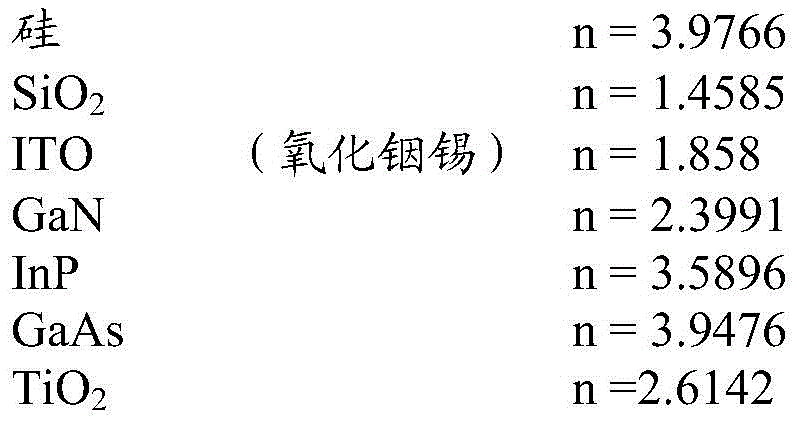
例如,TiO2可作为居间电介质材料来减少反射损耗。取决于存在的III-V化合物半导体202,也可使用电介质材料诸如铝掺杂氧化锌(AZO)和镓掺杂氧化锌(ZNO)。还可能的是,光学互连件位于氧化硅与GaN之间,因为氧化硅可充当光学波导。For example, TiO2 can be used as an intervening dielectric material to reduce reflection losses. Depending on the III-
光电子互连件200的光学零件也可通过配置III-V化合物半导体202的底表面与硅波导218的顶表面之间的光学厚度来优化。该厚度可以是在通过接合光电子管芯100和晶圆102而形成的每个光子器件中所使用的操作光(诸如1550nm下的红外光)的波长的四分之一的奇数倍。The optical components of the
取决于将键合到晶圆102的管芯100的基板230的厚度,可通过激光剥离、研磨、蚀刻等来移除基板230的层,以使正键合的管芯100变薄。然后,例如,可在管芯100的光电子器件202的顶部上添加反射层、金属或分布式布拉格反射器(DBR)232,以保持光被包含并且有利地反射到管芯100上的光电子器件202中。Depending on the thickness of the
图3示出了形成示例性光电子互连件200的相应的管芯100和晶圆102的示例性键合平面206和208的顶视图(或底视图)。相比之下,图2示出了侧视图。将直接键合在一起的电极212和222以及214和224的这种配置仅仅是一个示例性配置。在图4至图5中示出了其他示例性配置。FIG. 3 illustrates a top view (or bottom view) of
在图3中,在示例性实施方案中,形成在管芯100的一侧上的第一耦合平面206具有形成在耦合平面206中的第一光学键合区域204、围绕第一光学窗口204的外周边的第一电接触件212(该第一电接触件也设置在管芯100的耦合平面206中)并且具有围绕第一“内部”电接触件212的外周边的第二电接触件214,所有这些都设置在管芯100的耦合平面206中。In FIG. 3 , in an exemplary embodiment, a
用于高密度集成光子器件的电气互连件和光学互连件200的晶圆侧键合平面208包括耦合平面208中的晶圆侧光学窗口216、在光学窗口216的周边之外的晶圆102的第一电接触件222、在第一电接触件222的周边之外的晶圆102的第二电接触件224以及分别连接到第一电接触件222和第二电接触件224的电引线302和304,所有这些都设置在晶圆102的耦合平面208中。Wafer-
在一个实施方式中,晶圆102的光电子电路220的第二互补电接触件224在晶圆102的耦合平面208内为开环或其他不连续的平坦形状,并且在其开环或不连续形式中具有间隙300,以用于容纳从电路220到晶圆102的耦合平面208内的第一互补电接触件222的电气布线302。间隙300允许第二电接触件224与引线302或通向光电子电路220的第一电接触件222的其他导电线保持电绝缘。In one embodiment, the second complementary
管芯100的第一电接触件212和晶圆102的第一互补电接触件222可各自为例如围绕相应的第一光学窗口204和第二光学窗口216的正方形、矩形、圆形或椭圆形形式的导电线或迹线或环。The first
用于高密度集成光子器件的电气互连件和光学互连件200在接合时在管芯100的(第一)光学窗口204与晶圆102的(第二)光学窗口216之间具有电介质到电介质直接键合的光学互连件。电气互连件和光学互连件200还具有在管芯100的第一电接触件212和第二电接触件214与晶圆的互补的第一电接触件222和第二电接触件224之间的无焊料金属到金属直接键合的电气互连件。光学区域204和216以及相应的电接触件212和222以及214和224两者的直接键合形成完整的键合界面200,该键合界面经由管芯100与晶圆102之间的接合的耦合平面206和208形成高密度光电子互连件200的容量。The electrical and
尽管电接触件212、214、222和224在图3中被示出为暴露于表面,但在一种场景下,仅呈小焊盘形式的接触件的部分被暴露并且实际上被键合。并非所有CMP工艺都能够以环的形式使具有暴露的金属负载的键合表面平坦化,如图3所描绘。相反,在一些实施方式中,更均匀暴露的金属负载(分布的焊盘)可更适合于优化的CMP工艺。Although
尽管电接触件212、214、222和224被示出为形成为环形、正方形、矩形、圆形或椭圆形形状的导电线或迹线,但电接触件中的每个电接触件也可能仅呈一个(或多个)焊盘的形式,而不一定外接光学窗口204或206。另外,每个此类焊盘可通过导电通孔电连接到其管芯100。在图4至图5中示出焊盘键合实施方式的示例。Although
在管芯100与晶圆102之间形成直接键合的光电子互连件之后,可将晶圆102及其键合的管芯100切割或个体化为单独的光电子器件,或者切割或个体化为光电子器件组。对于一些应用,具有直接键合的管芯100的晶圆102可保持完整且未切割,其中光电子器件阵列在例如晶圆102的相对较大区段上,或在整个晶圆102上。After the direct-bonded optoelectronic interconnects are formed between the die 100 and the
图4示出了示例性光电子互连件200的实施方式,其中光子器件100的第一电接触件212和光子器件100的第二电接触件214各自为单个金属焊盘,被抛光并准备用于与正直接键合到的晶圆102的表面208上的互补焊盘222和224进行直接金属到金属键合。在不干扰光学区域204和216的直接键合的不同的直接键合区域中,将直接键合的接触件212和214均偏离光学区域204和216的一侧。为了键合可靠性,各个键合焊盘212和214或接触件可以是相应的焊盘的单个实例(左)或用于每个引线或线的焊盘的多个冗余实例(右)。当光子器件具有多于两个引线将跨光电子互连件200连接时,也可使用多个焊盘(右)。FIG. 4 illustrates an embodiment of an exemplary
将键合焊盘222和224耦合到正键合到的晶圆102的电路(诸如LED驱动器电路)的迹线或导线220和220'通常被嵌入或设置在键合表面208自身下方。Traces or
图5示出了示例性光电子互连件200的实施方式,其中光子器件100的第一电接触件212和光子器件100的第二电接触件214各自为金属焊盘,被抛光并准备用于进行直接金属到金属键合。互补焊盘222和224位于正直接键合到的晶圆102的表面208上。在该配置中,将直接键合的接触件212和214在将直接键合的光学区域204和216之外的两个或更多个侧面上、在一个或多个不妨碍光学路径或不妨碍光学区域204和216的表面之间的直接键合的不同直接键合区域中。为了键合可靠性,例如,如果冗余焊盘中的一个弱键合,则各个键合焊盘212和214或接触件可以是相应焊盘的单个实例(左),或者可以是用于每个线或引线的焊盘的多个冗余实例(右)。当光子器件具有多于两种类型的引线要跨光电子互连件200连接时,也可使用多个焊盘(右)。5 illustrates an embodiment of an exemplary
将键合焊盘222和224耦合到正键合到的晶圆102的电路(诸如LED驱动器电路)的迹线或导线220和220'通常被嵌入或设置在键合表面208自身下方。Traces or
图6示出了示例性设备600,其中光子器件(诸如LED、mLED或激光源阵列)形成或排列在晶圆602或重构的晶圆上以制造光子器件。正键合到的第二晶圆102可具有电子电路诸如CMOS驱动器电路,以通过电接触件212和214跨平坦的光电子界面(通过直接键合而接合的206和208)而直接键合在两个晶圆602和102之间来连接到第一晶圆602上的光子器件。为了形成光电子互连件,利用CMP或用于实现超平坦直接键合表面的其他技术来对光电子界面的两个表面206和208进行平坦化。正直接键合的表面206和208还可包括相应的光学键合区域206和216。除电子驱动器电路之外,第二晶圆102还可含有光子电路(光路),光通过波导218射入或照射到该光子电路中,这些波导直接键合到LED 100或其他光子器件的光学区域204。FIG. 6 shows an
直接混合键合(诸如
图7示出了另一个示例性设备700,其中光子器件诸如LED、mLED或激光源被排列在晶圆702上。正键合到的第二晶圆704可具有电子电路诸如CMOS驱动器电路,以通过电接触件706和708跨平坦的直接键合界面(接合到712的710)而直接键合在两个晶圆702和704之间来连接到第一晶圆702上的光子器件。FIG. 7 shows another
示例性设备700的两个晶圆702和704可利用直接混合键合工艺(诸如
在一个实施方式中,直接键合工艺形成薄mLED阵列700,其中具有LED结构的晶圆702直接键合到CMOS驱动器芯片晶圆704。In one embodiment, a
为了实现直接混合键合,在一个实施方式中,在mLED器件晶圆702上形成平坦并且激活的表面710之后,例如,利用CMP或获得超平坦表面的其他装置、以及等离子体激活718对CMOS晶圆704进行平坦化。To achieve direct hybrid bonding, in one embodiment, after forming a flat and activated surface 710 on the
然后,例如,在退火阶段期间,将两个晶圆702和704直接键合在非金属电介质表面714之间以及金属导体716之间。在非金属电介质表面在接触件上定向键合714之后,金属导体716的直接键合可在大约100℃至200℃的退火温度下进行,以形成金属和非金属两者的强大的直接键合互连,从而制备示例性mLED阵列700。The two
示例性方法Exemplary method
图8示出了形成适用于将管芯(该管芯包括光子器件,诸如III-V半导体光子器件)直接键合到晶圆诸如硅或SOI晶圆以形成用于集成光子器件的光电子互连件的平坦键合界面的示例性方法800。在一些实施方式中,光电子互连件可跨界面直接键合两个电接触件,并且可跨相同界面直接键合光学通路。在图8的流程图中,示例性方法800的操作以单独的框示出。Figure 8 illustrates the formation of optoelectronic interconnects suitable for direct bonding of dies comprising photonic devices, such as III-V semiconductor photonics devices, to wafers such as silicon or SOI wafers to form optoelectronic interconnects for integrated photonic devices
在框802处,在管芯的第一平坦键合表面中形成第一光学窗口,该管芯包括光子器件,诸如基于III-V半导体化合物的传感器或LED。At block 802, a first optical window is formed in a first flat bonding surface of a die that includes a photonic device, such as a III-V semiconductor compound based sensor or LED.
在框804处,在第一平坦键合表面中形成管芯的光子器件的第一电接触件,该第一电接触件至少部分地外接管芯的第一光学窗口。At block 804, a first electrical contact of the photonic device of the die is formed in the first flat bonding surface, the first electrical contact at least partially circumscribing the first optical window of the die.
在框806处,在第一平坦键合表面中形成管芯的光子器件的第二电接触件,该第二电接触件至少部分地外接第一电接触件。At
在框808处,在与晶圆相关联的第二平坦键合表面中形成与硅波导连通的第二光学窗口。At block 808, a second optical window in communication with the silicon waveguide is formed in a second planar bonding surface associated with the wafer.
在框810处,在第二平坦键合表面中形成晶圆的光电子电路的第一电接触件,该第一电接触件至少部分地外接硅或SOI晶圆的第二光学窗口。At block 810, a first electrical contact of the optoelectronic circuit of the wafer is formed in the second flat bonding surface, the first electrical contact at least partially circumscribing the second optical window of the silicon or SOI wafer.
在框812处,在第二平坦键合表面中形成晶圆的光电子电路的第二电接触件,该第二电接触件至少部分地外接第二平坦键合表面的第一电接触件。At block 812, a second electrical contact of the optoelectronic circuit of the wafer is formed in the second flat bonding surface, the second electrical contact at least partially circumscribing the first electrical contact of the second flat bonding surface.
例如,分别使管芯和晶圆的第一平坦键合表面和第二平坦键合表面足够平坦以用于通过CMP进行直接键合工艺。相应的光学窗口通过例如电介质到电介质直接键合工艺(例如,氧化物到氧化物直接键合工艺)而跨键合界面彼此直接键合。相应的共面金属电接触件使用金属到金属直接键合工艺而跨键合界面彼此直接键合。当利用直接混合键合(例如,
在管芯与晶圆之间形成直接键合的光电子互连件之后,具有键合的管芯的实例的晶圆可被切割或个体化为单独的光电子器件、或者被切割或个体化为光电子器件组。对于一些应用诸如模拟相机传感器,具有直接键合的管芯的晶圆可保持未切割,其中光电子器件的阵列在晶圆的相对较大区段上形成相机传感器的栅格。After the direct-bonded optoelectronic interconnects are formed between the die and the wafer, the wafer with instances of the bonded die may be diced or singulated into individual optoelectronic devices, or diced or singulated into optoelectronics device group. For some applications such as analog camera sensors, wafers with directly bonded dies may remain uncleaved, where the array of optoelectronic devices forms a grid of camera sensors over a relatively large section of the wafer.
光子器件还可定位在其自身的晶圆上,以直接键合到承载CMOS电路或其他光电子电路的另一个晶圆,从而提供用于制备例如mLED阵列的晶圆到晶圆(W2W)工艺。A photonic device can also be positioned on its own wafer for direct bonding to another wafer carrying CMOS circuits or other optoelectronic circuits, providing a wafer-to-wafer (W2W) process for fabricating, for example, mLED arrays.
图9示出了将包括光子器件(诸如III-V半导体光子器件)的管芯键合到硅晶圆或绝缘体上硅(SOI)晶圆以形成用于高密度集成光子器件的光电子互连件的示例性方法900。在图9的流程图中,示例性方法900的操作以单独的框示出。9 illustrates bonding of a die including a photonic device, such as a III-V semiconductor photonic device, to a silicon wafer or a silicon-on-insulator (SOI) wafer to form optoelectronic interconnects for high-density integrated photonic devices
在框902处,在包括光子器件的管芯上,基于具有经完全处理的金属接触件的III-V半导体化合物形成第一平坦键合界面。At
在框904处,在硅或SOI晶圆上形成第二平坦键合界面。At
在框906处,将管芯的第一平坦键合界面和硅或SOI晶圆的第二平坦键合界面的相应的光学窗口直接键合在一起以在管芯与硅或SOI晶圆之间形成光学互连件。At
在框908处,将管芯的第一平坦键合界面和硅或SOI晶圆的第二平坦键合界面的相应的第一电接触件直接键合在一起,以在管芯与硅或SOI晶圆之间形成第一电气互连件。At
在框910处,将管芯的第一平坦键合界面和硅晶圆或晶圆的第二平坦键合界面的相应的第二电接触件直接键合在一起,以在管芯与硅或SOI晶圆之间形成第二电气互连件。At
共面的光学窗口、第一电极和第二电极能够进行直接键合操作,诸如直接混合键合(例如,
在本说明书和以下权利要求书中:术语“连接(connect)”、“连接(connection)”、“连接(connected)”、“连接(in connection with)”和“连接(connecting)”用于表示“直接连接”或“通过一个或多个元件连接”。术语“联接(couple)”、“联接(coupling)”、“联接(coupled)”、“联接在一起”和“联接(coupled with)”是指“直接联接在一起”或“通过一个或多个元件联接在一起”。In this specification and the following claims: the terms "connect", "connection", "connected", "in connection with" and "connecting" are used to mean "Directly connected" or "connected through one or more elements". The terms "couple", "coupling", "coupled", "coupled together" and "coupled with" mean "coupled directly together" or "through one or more elements together".
虽然已结合有限数目的实施方案公开了本公开,但本领域的技术人员将会理解,在给出本公开的有益效果的情况下,可以根据本发明进行可能的多种修改和变型。所附权利要求旨在涵盖属于本公开的真正实质和范围内的此类修改形式和变型形式。Although the present disclosure has been disclosed in connection with a limited number of embodiments, those skilled in the art will appreciate that various modifications and variations are possible in accordance with the present invention, given the benefits of this disclosure. The appended claims are intended to cover such modifications and variations as fall within the true spirit and scope of the present disclosure.
权利要求书(按照条约第19条的修改)Claims (as amended by Article 19 of the Treaty)
1.一种直接键合的光电子互连件,包括: 1. A directly bonded optoelectronic interconnect comprising:
第一管芯或晶圆的第一键合平面,所述第一键合平面包括第一光学窗口和所述第一管芯或晶圆的光子器件的电接触件; a first bonding plane of a first die or wafer, said first bonding plane comprising a first optical window and electrical contacts of photonic devices of said first die or wafer;
第二管芯或晶圆的第二键合平面,所述第二键合平面包括第二光学窗口和所述第二管芯或晶圆的电接触件;以及 a second bond plane of a second die or wafer, the second bond plane including a second optical window and electrical contacts of the second die or wafer; and
直接键合在一起的所述第一管芯或晶圆和所述第二管芯或晶圆的所述光学窗口;以及 the optical window of the first die or wafer and the second die or wafer directly bonded together; and
直接键合在一起的所述第一管芯或晶圆和所述第二管芯或晶圆的所述相应的电接触件。 The respective electrical contacts of the first die or wafer and the second die or wafer are directly bonded together.
2.根据权利要求1所述的直接键合的光电子互连件,其中所述第一管芯或晶圆的所述电接触件至少部分地外接所述第一管芯或晶圆的所述第一光学窗口,或者所述第二管芯或晶圆的所述电接触件至少部分地外接所述第二管芯或晶圆的所述第二光学窗口。
2. The directly bonded optoelectronic interconnect of
3.根据权利要求1所述的直接键合的光电子互连件,其中所述第一光学窗口和所述第二光学窗口通过电介质到电介质直接键合而无需单独的粘合剂或通过直接混合键合操作的直接键合来直接键合在一起;并且
3. The directly bonded optoelectronic interconnect of
其中所述第一管芯的所述电接触件和所述第二管芯的所述电接触件通过金属到金属直接键合或通过所述直接混合键合操作的直接键合来直接键合在一起。 wherein the electrical contacts of the first die and the electrical contacts of the second die are directly bonded by direct metal-to-metal bonding or direct bonding by the direct hybrid bonding operation together.
4.根据权利要求1所述的直接键合的光电子互连件,还包括:
4. The directly bonded optoelectronic interconnect of
第一键合平面,所述第一键合平面与所述第一管芯相关联,所述第一键合平面包括:所述第一光学窗口、至少部分地外接所述第一光学窗口并且与所述第一光学窗口共面的第一电接触件和至少部分地外接所述第一电接触件并且与所述第一电接触件和所述第一光学窗口两者共面的第二电接触件;和 a first bonding plane associated with the first die, the first bonding plane comprising the first optical window, at least partially circumscribing the first optical window, and a first electrical contact coplanar with the first optical window and a second electrical contact at least partially circumscribing the first electrical contact and coplanar with both the first electrical contact and the first optical window electrical contacts; and
第二键合平面,所述第二键合平面与所述第二管芯相关联,所述第二键合平面包括:所述第二光学窗口、所述第二管芯的至少部分地外接所述第二光学窗口并且与所述第二光学窗口共面的第一电接触件和所述第二管芯的至少部分地外接所述第二管芯的所述第一电接触件并且与所述第二管芯的所述第一电接触件和所述第二光学窗口两者共面的第二电接触件。 A second bond plane associated with the second die, the second bond plane comprising: the second optical window, at least partially circumscribed by the second die a first electrical contact of the second optical window and coplanar with the second optical window and the first electrical contact of the second die at least partially circumscribing the second die and with The first electrical contact of the second die and the second electrical contact of the second optical window are both coplanar.
5.一种设备,包括: 5. An apparatus comprising:
第一管芯,所述第一管芯包括光电子器件; a first die, the first die comprising an optoelectronic device;
所述第一管芯的光学耦合区域,所述光学耦合区域与所述光电子器件光学连通; an optical coupling region of the first die, the optical coupling region being in optical communication with the optoelectronic device;
所述第一管芯的耦合平面,所述耦合平面用于与第二管芯的互补耦合平面光学耦合和电耦合,所述第一管芯的所述耦合平面的一部分含有所述第一管芯的所述光学耦合区域; a coupling plane of the first die for optical and electrical coupling with a complementary coupling plane of a second die, a portion of the coupling plane of the first die containing the first die the optical coupling region of the core;
所述光电子器件的第一电接触件,所述第一电接触件设置在所述第一管芯的所述耦合平面中的所述光学耦合区域的周边之外;和 a first electrical contact of the optoelectronic device disposed outside the perimeter of the optical coupling region in the coupling plane of the first die; and
所述光电子器件的第二电接触件,所述第二电接触件设置在所述第一管芯的所述耦合平面中的所述第一电接触件的周边之外。 A second electrical contact of the optoelectronic device disposed outside the perimeter of the first electrical contact in the coupling plane of the first die.
6.根据权利要求5所述的设备,其中所述第一电接触件完全围绕所述第一管芯的所述耦合平面中的所述光学耦合区域;并且 6. The apparatus of claim 5, wherein the first electrical contact completely surrounds the optical coupling region in the coupling plane of the first die; and
其中所述第一管芯的所述光电子器件的所述第一电接触件设置在所述第二管芯的硅波导的光学耦合区域的周边之外。 wherein the first electrical contact of the optoelectronic device of the first die is disposed outside the perimeter of the optical coupling region of the silicon waveguide of the second die.
7.根据权利要求5所述的设备,还包括: 7. The apparatus of claim 5, further comprising:
第二管芯,其中在接合所述第一管芯和所述第二管芯的相应的耦合平面时,所述第一管芯能够与所述第二管芯光学耦合和电耦合; a second die, wherein the first die can be optically and electrically coupled with the second die upon bonding of the respective coupling planes of the first die and the second die;
所述第二管芯中的硅波导,所述硅波导与所述第二管芯的光学耦合区域光学连通; a silicon waveguide in the second die, the silicon waveguide in optical communication with an optical coupling region of the second die;
所述第二管芯的所述光学耦合区域,所述光学耦合区域占据所述第二管芯的所述耦合平面的一部分; the optical coupling region of the second die, the optical coupling region occupying a portion of the coupling plane of the second die;
所述第二管芯的光电子电路; the optoelectronic circuit of the second die;
所述光电子电路的第一电接触件,所述第一电接触件设置在所述第二管芯的所述耦合平面中的所述第二管芯的所述光学耦合区域的周边之外,所述光电子电路的所述第一电接触件与所述第一管芯的所述第一电接触件的平坦几何轮廓匹配;和 a first electrical contact of the optoelectronic circuit, the first electrical contact being disposed outside the perimeter of the optical coupling region of the second die in the coupling plane of the second die, the first electrical contact of the optoelectronic circuit matches a flat geometric profile of the first electrical contact of the first die; and
所述光电子电路的第二电接触件,所述第二电接触件设置在所述第二管芯的所述耦合平面中的所述光电子电路的所述第一电接触件的周边之外,所述光电子电路的所述第二电接触件与所述第一管芯的所述第二电接触件的平坦几何轮廓匹配。 a second electrical contact of the optoelectronic circuit disposed outside the perimeter of the first electrical contact of the optoelectronic circuit in the coupling plane of the second die, The second electrical contact of the optoelectronic circuit matches a flat geometric profile of the second electrical contact of the first die.
8.根据权利要求7所述的设备,其中从所述第二管芯的所述光电子电路到所述光电子电路的所述第一电接触件和所述第二电接触件的电气布线在所述第二管芯的所述耦合平面内。 8. The apparatus of claim 7, wherein electrical routing from the optoelectronic circuit of the second die to the first and second electrical contacts of the optoelectronic circuit is within the coupling plane of the second die.
9.根据权利要求8所述的设备,其中所述光电子电路的所述第二电接触件包括在所述第二管芯的所述耦合平面内的开环或不连续迹线,还包括在所述开环或所述不连续迹线中的间隙,用于容纳到所述第二管芯的所述耦合平面内的所述光电子电路的所述第一电接触件的所述电气布线。 9. The apparatus of claim 8, wherein the second electrical contact of the optoelectronic circuit comprises an open loop or discontinuous trace within the coupling plane of the second die, further comprising A gap in the open loop or the discontinuous trace for accommodating the electrical routing to the first electrical contact of the optoelectronic circuit within the coupling plane of the second die.
10.根据权利要求7所述的设备,其中所述第二管芯的所述光学耦合区域至少包括光栅表面,用于在所述第一管芯和所述第二管芯之间进行光学模式匹配耦合。 10. The apparatus of claim 7, wherein the optical coupling region of the second die includes at least a grating surface for optical modes between the first die and the second die matching coupling.
11.根据权利要求10所述的设备,其中对于单模红外透射,所述光栅表面小于10微米(μ)厚。 11. The apparatus of claim 10, wherein the grating surface is less than 10 micrometers ([mu]) thick for single mode infrared transmission.
12.根据权利要求5所述的设备,其中所述第一管芯在接合到所述第二管芯之前,具有所述光电子器件的经完全处理的电极以及所述光电子器件的经完全处理的第一电接触件和第二电接触件。 12. The apparatus of claim 5, wherein the first die has fully processed electrodes of the optoelectronic device and fully processed electrodes of the optoelectronic device prior to bonding to the second die A first electrical contact and a second electrical contact.
13.根据权利要求5所述的设备,还包括: 13. The apparatus of claim 5, further comprising:
在接合耦合平面中在所述第一管芯的所述光学耦合区域与所述第二管芯的所述光学耦合区域之间的光学耦合; optical coupling between the optical coupling region of the first die and the optical coupling region of the second die in a bond coupling plane;
在所述接合耦合平面中在所述第一管芯的所述光电子器件的所述第一电接触件与所述第二管芯的所述光电子电路的所述第一电接触件之间的金属到金属键合或直接混合键合;以及 in the bond coupling plane between the first electrical contact of the optoelectronic device of the first die and the first electrical contact of the optoelectronic circuit of the second die metal-to-metal bonding or direct hybrid bonding; and
在所述接合耦合平面中在所述第一管芯的所述光电子器件的所述第二电接触件与所述第二管芯的所述光电子电路的所述第二电接触件之间的金属到金属键合或直接混合键合。 in the bond coupling plane between the second electrical contact of the optoelectronic device of the first die and the second electrical contact of the optoelectronic circuit of the second die Metal-to-metal bonding or direct hybrid bonding.
14.根据权利要求13所述的设备,还包括在III-V化合物半导体与所述硅波导之间的透明导电氧化物(TCO),以增强进入所述III-V化合物半导体的导电性并增强所述导电性的均匀性。 14. The apparatus of claim 13, further comprising a transparent conductive oxide (TCO) between the III-V compound semiconductor and the silicon waveguide to enhance conductivity into the III-V compound semiconductor and enhance the uniformity of the conductivity.
15.根据权利要求14所述的设备,其中所述透明导电氧化物(TCO)选自由以下项组成的组:铝掺杂氧化锌(AZO)、镓掺杂氧化锌(GZO)和氧化铟锡(ITO)。 15. The apparatus of claim 14, wherein the transparent conductive oxide (TCO) is selected from the group consisting of aluminum doped zinc oxide (AZO), gallium doped zinc oxide (GZO), and indium tin oxide (ITO).
16.根据权利要求5所述的设备,还包括III-V化合物半导体的底表面,通过蚀刻而使所述底表面粗糙化以减少反射损耗。 16. The apparatus of claim 5, further comprising a bottom surface of the III-V compound semiconductor, the bottom surface being roughened by etching to reduce reflection losses.
17.根据权利要求5所述的设备,还包括电介质材料,所述电介质材料在III-V化合物半导体的所述底表面与所述硅波导之间,以减少所述III-V化合物半导体与所述硅波导之间的反射损耗,其中所述电介质材料的折射率在所述硅的所述折射率与所述III-V化合物半导体的所述折射率之间。 17. The apparatus of claim 5, further comprising a dielectric material between the bottom surface of the III-V compound semiconductor and the silicon waveguide to reduce the effect of the III-V compound semiconductor on the reflection loss between the silicon waveguides, wherein the refractive index of the dielectric material is between the refractive index of the silicon and the refractive index of the III-V compound semiconductor.
18.根据权利要求17所述的设备,其中所述III-V化合物半导体的所述底表面与所述硅波导的顶表面之间的光学厚度为所述设备的操作光的波长的四分之一的奇数倍。 18. The device of claim 17, wherein the optical thickness between the bottom surface of the III-V compound semiconductor and the top surface of the silicon waveguide is one-fourth the wavelength of the operating light of the device Odd multiples of one.
19.根据权利要求18所述的设备,还包括反射层,所述反射层在与所述键合表面相对的所述表面上在所述第一管芯的所述光电子器件的顶部上。 19. The apparatus of claim 18, further comprising a reflective layer on top of the optoelectronic device of the first die on the surface opposite the bonding surface.
20.一种用于高密度集成光子器件的电气互连件和光学互连件,包括: 20. An electrical and optical interconnect for a high density integrated photonic device, comprising:
第一耦合平面,所述第一耦合平面形成在第一管芯的一侧上; a first coupling plane formed on one side of the first die;
第一光学窗口,所述第一光学窗口形成在所述第一管芯的所述耦合平面中; a first optical window formed in the coupling plane of the first die;
第一电接触件,所述第一电接触件在所述第一光学窗口的周边之外并且设置在所述第一管芯的所述耦合平面中;和 a first electrical contact outside the perimeter of the first optical window and disposed in the coupling plane of the first die; and
第二电接触件,所述第二电接触件在所述第一电接触件的周边之外并且设置在所述第一管芯的所述耦合平面中。 A second electrical contact outside the perimeter of the first electrical contact and disposed in the coupling plane of the first die.
21.根据权利要求20所述的用于高密度集成光子器件的电气互连件和光学互连件,还包括: 21. The electrical and optical interconnects for high density integrated photonic devices of claim 20, further comprising:
第二耦合平面,所述第二耦合平面形成在第二管芯上; a second coupling plane formed on the second die;
第二光学窗口,所述第二光学窗口在所述第二管芯的所述耦合平面中; a second optical window in the coupling plane of the second die;
第一互补电接触件,所述第一互补电接触件在所述第二光学窗口的周边之外并且设置在所述第二管芯的所述耦合平面中; a first complementary electrical contact outside the perimeter of the second optical window and disposed in the coupling plane of the second die;
第二互补电接触件,所述第二互补电接触件在所述第一互补电接触件的周边之外并且设置在所述第二管芯的所述耦合平面中;和 a second complementary electrical contact outside the perimeter of the first complementary electrical contact and disposed in the coupling plane of the second die; and
电引线,所述电引线通向设置在所述第二管芯的所述耦合平面中的所述第一互补电接触件和所述第二互补电接触件。 Electrical leads leading to the first and second complementary electrical contacts disposed in the coupling plane of the second die.
22.根据权利要求20所述的用于高密度集成光子器件的电气互连件和光学互连件,其中所述第一管芯的所述第一电接触件和所述第二管芯的所述第一互补电接触件各自包括围绕相应的第一光学窗口或第二光学窗口的正方形、矩形、圆形或椭圆形导电线。 22. The electrical and optical interconnects for high density integrated photonic devices of claim 20, wherein the first electrical contacts of the first die and the second die The first complementary electrical contacts each comprise square, rectangular, circular or oval conductive lines surrounding the respective first or second optical window.
23.根据权利要求20所述的用于高密度集成光子器件的电气互连件和光学互连件,还包括在所述第一管芯的所述第一光学窗口与所述第二管芯的所述第二光学窗口之间的电介质到电介质光学互连件,以及在所述第一管芯的所述第一电接触件和所述第二电接触件与所述第二管芯的所述第一互补电接触件和所述第二互补电接触件之间的无焊金属到金属键合电气互连件或直接混合键合互连件,从而在所述第一管芯和所述第二管芯的接合耦合平面上形成高密度电气互连件。 23. The electrical and optical interconnects for high density integrated photonic devices of claim 20, further comprising the first optical window and the second die in the first die the dielectric-to-dielectric optical interconnect between the second optical window, and the first electrical contact and the second electrical contact on the first die and the second die Solderless metal-to-metal bonding electrical interconnects or direct hybrid bonding interconnects between the first complementary electrical contact and the second complementary electrical contact so that the first die and all High density electrical interconnects are formed on the bond coupling plane of the second die.
24.一种方法,包括: 24. A method comprising:
将光电子管芯直接键合到晶圆,包括: Bonding optoelectronic dies directly to wafers, including:
在与在所述光电子管芯与所述晶圆之间形成电气互连件的相同的共面键合界面上在所述光电子管芯与所述晶圆之间形成直接键合光学互连件;以及 Forms direct bond optical interconnects between the optoelectronic die and the wafer on the same coplanar bonding interface that forms the electrical interconnects between the optoelectronic die and the wafer ;as well as
在与在所述光电子管芯与所述晶圆之间形成所述光学互连件相同的共面键合界面上在所述光电子管芯的所述金属接触件与所述晶圆的互补金属接触件之间形成至少一个金属到金属直接键合电气互连件。 Complementary metal between the metal contacts of the optoelectronic die and the wafer at the same coplanar bonding interface that forms the optical interconnects between the optoelectronic die and the wafer At least one metal-to-metal direct bond electrical interconnect is formed between the contacts.
25.根据权利要求24所述的方法,还包括: 25. The method of claim 24, further comprising:
在所述光电子管芯的耦合平面上形成第一光学耦合区域、第一电接触件和第二电接触件,其中所述第一光学耦合区域、所述第一电接触件和所述第二电接触件是共面的,并且其中所述第一电接触件和所述第二电接触件设置在所述光电子管芯的所述第一光学耦合区域的光学路径之外;以及 A first optical coupling region, a first electrical contact and a second electrical contact are formed on the coupling plane of the optoelectronic die, wherein the first optical coupling region, the first electrical contact and the second electrical contact the electrical contacts are coplanar, and wherein the first electrical contact and the second electrical contact are disposed outside the optical path of the first optical coupling region of the optoelectronic die; and
在所述晶圆的耦合平面上形成第二光学耦合区域、第一互补电接触件和第二互补电接触件,其中所述第二光学耦合区域、所述第一互补电接触件和所述第二互补电接触件是共面的,并且其中所述第一互补电接触件和所述第二互补电接触件设置在所述晶圆的所述第二光学耦合区域的光学路径之外。 A second optical coupling region, a first complementary electrical contact and a second complementary electrical contact are formed on the coupling plane of the wafer, wherein the second optical coupling region, the first complementary electrical contact and the The second complementary electrical contact is coplanar, and wherein the first complementary electrical contact and the second complementary electrical contact are disposed out of the optical path of the second optical coupling region of the wafer.
26.根据权利要求24所述的方法,还包括将所述晶圆和所述管芯的实例切割成单独的光子器件。 26. The method of claim 24, further comprising dicing the wafer and instances of the die into individual photonic devices.
27.一种设备,包括: 27. An apparatus comprising:
光子器件,所述光子器件在相应管芯上或第一晶圆上; a photonic device, the photonic device is on the corresponding die or on the first wafer;
每个光子器件包括电接触件和光学通路; each photonic device includes electrical contacts and optical pathways;
第二晶圆,所述第二晶圆包括用于所述光子器件的电路的电接触件和光学波导; a second wafer including electrical contacts and optical waveguides for circuits of the photonic device;
非金属直接键合,所述非金属直接键合在所述相应管芯或第一晶圆的所述光子器件的所述光学通路之间; non-metallic direct bonding between the optical vias of the photonic devices of the corresponding die or first wafer;
金属直接键合,所述金属直接键合在所述相应管芯或第一晶圆的所述光子器件的所述电接触件与所述第二晶圆的所述电路的所述电接触件之间。 Metal direct bonding, the metal is directly bonded to the electrical contacts of the photonic devices of the corresponding die or first wafer and the electrical contacts of the circuits of the second wafer between.
28.根据权利要求27所述的设备,其中所述光子器件包括激光器、光电探测器、光学二极管、LED或微型LED。 28. The apparatus of claim 27, wherein the photonic device comprises a laser, a photodetector, an optical diode, an LED, or a micro LED.
Claims (28)
Applications Claiming Priority (5)
| Application Number | Priority Date | Filing Date | Title |
|---|---|---|---|
| US201762599146P | 2017-12-15 | 2017-12-15 | |
| US62/599,146 | 2017-12-15 | ||
| US16/219,693 | 2018-12-13 | ||
| US16/219,693 US11011503B2 (en) | 2017-12-15 | 2018-12-13 | Direct-bonded optoelectronic interconnect for high-density integrated photonics |
| PCT/US2018/065687 WO2019118846A1 (en) | 2017-12-15 | 2018-12-14 | Direct-bonded optoelectronic interconnect for high-density integrated photonics |
Publications (1)
| Publication Number | Publication Date |
|---|---|
| CN111480236A true CN111480236A (en) | 2020-07-31 |
Family
ID=66816344
Family Applications (1)
| Application Number | Title | Priority Date | Filing Date |
|---|---|---|---|
| CN201880080463.XA Pending CN111480236A (en) | 2017-12-15 | 2018-12-14 | Directly bonded optoelectronic interconnects for high density integrated photonic devices |
Country Status (3)
| Country | Link |
|---|---|
| US (2) | US11011503B2 (en) |
| CN (1) | CN111480236A (en) |
| WO (1) | WO2019118846A1 (en) |
Cited By (6)
| Publication number | Priority date | Publication date | Assignee | Title |
|---|---|---|---|---|
| CN114551494A (en) * | 2022-02-28 | 2022-05-27 | 华引芯(武汉)科技有限公司 | Micro photoelectronic device and preparation method thereof |
| WO2022161427A1 (en) * | 2021-02-01 | 2022-08-04 | 北京与光科技有限公司 | Manufacturing method for optical device, and optical device |
| CN117111213A (en) * | 2023-09-01 | 2023-11-24 | 湖北江城芯片中试服务有限公司 | Silicon optical chip and manufacturing method thereof |
| WO2024007586A1 (en) * | 2022-07-05 | 2024-01-11 | 杭州视光半导体科技有限公司 | Method for preparing wafer having three-layer stacked structure, and application thereof |
| CN119828367A (en) * | 2025-01-26 | 2025-04-15 | 国科光芯金杏(北京)实验室科技有限公司 | Composite waveguide structure and preparation method thereof |
| TWI914623B (en) | 2023-05-25 | 2026-02-11 | 台灣積體電路製造股份有限公司 | Package structure and method for forming the same |
Families Citing this family (115)
| Publication number | Priority date | Publication date | Assignee | Title |
|---|---|---|---|---|
| US7109092B2 (en) | 2003-05-19 | 2006-09-19 | Ziptronix, Inc. | Method of room temperature covalent bonding |
| US8735219B2 (en) | 2012-08-30 | 2014-05-27 | Ziptronix, Inc. | Heterogeneous annealing method and device |
| US10886250B2 (en) | 2015-07-10 | 2021-01-05 | Invensas Corporation | Structures and methods for low temperature bonding using nanoparticles |
| US9953941B2 (en) | 2015-08-25 | 2018-04-24 | Invensas Bonding Technologies, Inc. | Conductive barrier direct hybrid bonding |
| US10204893B2 (en) | 2016-05-19 | 2019-02-12 | Invensas Bonding Technologies, Inc. | Stacked dies and methods for forming bonded structures |
| US11176450B2 (en) | 2017-08-03 | 2021-11-16 | Xcelsis Corporation | Three dimensional circuit implementing machine trained network |
| US10580735B2 (en) | 2016-10-07 | 2020-03-03 | Xcelsis Corporation | Stacked IC structure with system level wiring on multiple sides of the IC die |
| US10672663B2 (en) | 2016-10-07 | 2020-06-02 | Xcelsis Corporation | 3D chip sharing power circuit |
| TWI822659B (en) | 2016-10-27 | 2023-11-21 | 美商艾德亞半導體科技有限責任公司 | Structures and methods for low temperature bonding |
| US10002844B1 (en) | 2016-12-21 | 2018-06-19 | Invensas Bonding Technologies, Inc. | Bonded structures |
| US20180182665A1 (en) | 2016-12-28 | 2018-06-28 | Invensas Bonding Technologies, Inc. | Processed Substrate |
| CN117878055A (en) | 2016-12-28 | 2024-04-12 | 艾德亚半导体接合科技有限公司 | Stacking substrate processing |
| TW202431592A (en) | 2016-12-29 | 2024-08-01 | 美商艾德亞半導體接合科技有限公司 | Bonded structures with integrated passive component |
| WO2018169968A1 (en) | 2017-03-16 | 2018-09-20 | Invensas Corporation | Direct-bonded led arrays and applications |
| US10515913B2 (en) | 2017-03-17 | 2019-12-24 | Invensas Bonding Technologies, Inc. | Multi-metal contact structure |
| US10508030B2 (en) | 2017-03-21 | 2019-12-17 | Invensas Bonding Technologies, Inc. | Seal for microelectronic assembly |
| US10269756B2 (en) | 2017-04-21 | 2019-04-23 | Invensas Bonding Technologies, Inc. | Die processing |
| US10879212B2 (en) | 2017-05-11 | 2020-12-29 | Invensas Bonding Technologies, Inc. | Processed stacked dies |
| US10446441B2 (en) | 2017-06-05 | 2019-10-15 | Invensas Corporation | Flat metal features for microelectronics applications |
| US10217720B2 (en) | 2017-06-15 | 2019-02-26 | Invensas Corporation | Multi-chip modules formed using wafer-level processing of a reconstitute wafer |
| US10840205B2 (en) | 2017-09-24 | 2020-11-17 | Invensas Bonding Technologies, Inc. | Chemical mechanical polishing for hybrid bonding |
| US11031285B2 (en) | 2017-10-06 | 2021-06-08 | Invensas Bonding Technologies, Inc. | Diffusion barrier collar for interconnects |
| US11380597B2 (en) | 2017-12-22 | 2022-07-05 | Invensas Bonding Technologies, Inc. | Bonded structures |
| US10727219B2 (en) | 2018-02-15 | 2020-07-28 | Invensas Bonding Technologies, Inc. | Techniques for processing devices |
| US11169326B2 (en) | 2018-02-26 | 2021-11-09 | Invensas Bonding Technologies, Inc. | Integrated optical waveguides, direct-bonded waveguide interface joints, optical routing and interconnects |
| US11256004B2 (en) | 2018-03-20 | 2022-02-22 | Invensas Bonding Technologies, Inc. | Direct-bonded lamination for improved image clarity in optical devices |
| US10991804B2 (en) | 2018-03-29 | 2021-04-27 | Xcelsis Corporation | Transistor level interconnection methodologies utilizing 3D interconnects |
| US11056348B2 (en) | 2018-04-05 | 2021-07-06 | Invensas Bonding Technologies, Inc. | Bonding surfaces for microelectronics |
| US11244916B2 (en) | 2018-04-11 | 2022-02-08 | Invensas Bonding Technologies, Inc. | Low temperature bonded structures |
| US10790262B2 (en) | 2018-04-11 | 2020-09-29 | Invensas Bonding Technologies, Inc. | Low temperature bonded structures |
| US10964664B2 (en) | 2018-04-20 | 2021-03-30 | Invensas Bonding Technologies, Inc. | DBI to Si bonding for simplified handle wafer |
| US11004757B2 (en) | 2018-05-14 | 2021-05-11 | Invensas Bonding Technologies, Inc. | Bonded structures |
| US11276676B2 (en) | 2018-05-15 | 2022-03-15 | Invensas Bonding Technologies, Inc. | Stacked devices and methods of fabrication |
| US10923413B2 (en) | 2018-05-30 | 2021-02-16 | Xcelsis Corporation | Hard IP blocks with physically bidirectional passageways |
| CN112585740B (en) | 2018-06-13 | 2025-05-13 | 隔热半导体粘合技术公司 | TSV as a pad |
| US11393779B2 (en) | 2018-06-13 | 2022-07-19 | Invensas Bonding Technologies, Inc. | Large metal pads over TSV |
| US10910344B2 (en) | 2018-06-22 | 2021-02-02 | Xcelsis Corporation | Systems and methods for releveled bump planes for chiplets |
| WO2020010056A1 (en) | 2018-07-03 | 2020-01-09 | Invensas Bonding Technologies, Inc. | Techniques for joining dissimilar materials in microelectronics |
| US11158606B2 (en) | 2018-07-06 | 2021-10-26 | Invensas Bonding Technologies, Inc. | Molded direct bonded and interconnected stack |
| US11462419B2 (en) | 2018-07-06 | 2022-10-04 | Invensas Bonding Technologies, Inc. | Microelectronic assemblies |
| US12406959B2 (en) | 2018-07-26 | 2025-09-02 | Adeia Semiconductor Bonding Technologies Inc. | Post CMP processing for hybrid bonding |
| US11515291B2 (en) | 2018-08-28 | 2022-11-29 | Adeia Semiconductor Inc. | Integrated voltage regulator and passive components |
| US11296044B2 (en) | 2018-08-29 | 2022-04-05 | Invensas Bonding Technologies, Inc. | Bond enhancement structure in microelectronics for trapping contaminants during direct-bonding processes |
| US11011494B2 (en) | 2018-08-31 | 2021-05-18 | Invensas Bonding Technologies, Inc. | Layer structures for making direct metal-to-metal bonds at low temperatures in microelectronics |
| US11158573B2 (en) | 2018-10-22 | 2021-10-26 | Invensas Bonding Technologies, Inc. | Interconnect structures |
| FR3089442B1 (en) * | 2018-12-05 | 2020-12-18 | Airbus Operations Sas | A method of assembling at least two parts by transparency welding, a method of assembling a primary structure of an aircraft mast by transparency welding, the primary structure of an aircraft mast thus obtained and an aircraft comprising said primary structure |
| US11244920B2 (en) | 2018-12-18 | 2022-02-08 | Invensas Bonding Technologies, Inc. | Method and structures for low temperature device bonding |
| US11476213B2 (en) | 2019-01-14 | 2022-10-18 | Invensas Bonding Technologies, Inc. | Bonded structures without intervening adhesive |
| US11387202B2 (en) | 2019-03-01 | 2022-07-12 | Invensas Llc | Nanowire bonding interconnect for fine-pitch microelectronics |
| EP3935763A4 (en) | 2019-03-06 | 2022-12-07 | Lightmatter, Inc. | PHOTONICS COMMUNICATION PLATFORM |
| US11901281B2 (en) | 2019-03-11 | 2024-02-13 | Adeia Semiconductor Bonding Technologies Inc. | Bonded structures with integrated passive component |
| US10854578B2 (en) | 2019-03-29 | 2020-12-01 | Invensas Corporation | Diffused bitline replacement in stacked wafer memory |
| US11610846B2 (en) | 2019-04-12 | 2023-03-21 | Adeia Semiconductor Bonding Technologies Inc. | Protective elements for bonded structures including an obstructive element |
| US11373963B2 (en) | 2019-04-12 | 2022-06-28 | Invensas Bonding Technologies, Inc. | Protective elements for bonded structures |
| US11205625B2 (en) | 2019-04-12 | 2021-12-21 | Invensas Bonding Technologies, Inc. | Wafer-level bonding of obstructive elements |
| US11355404B2 (en) | 2019-04-22 | 2022-06-07 | Invensas Bonding Technologies, Inc. | Mitigating surface damage of probe pads in preparation for direct bonding of a substrate |
| US11430658B2 (en) * | 2019-05-07 | 2022-08-30 | Meta Platforms Technologies, Llc | Bonding methods for light emitting diodes |
| US11385278B2 (en) | 2019-05-23 | 2022-07-12 | Invensas Bonding Technologies, Inc. | Security circuitry for bonded structures |
| US12374641B2 (en) | 2019-06-12 | 2025-07-29 | Adeia Semiconductor Bonding Technologies Inc. | Sealed bonded structures and methods for forming the same |
| US11296053B2 (en) | 2019-06-26 | 2022-04-05 | Invensas Bonding Technologies, Inc. | Direct bonded stack structures for increased reliability and improved yield in microelectronics |
| EP3991204B1 (en) | 2019-06-27 | 2025-06-11 | Avicenatech, Corp. | Chip-scale optical interconnect using microleds |
| EP4029165A4 (en) | 2019-09-13 | 2022-11-09 | Avicenatech Corp. | OPTICAL INTERCONNECTIONS USING MICRODELS |
| US12080672B2 (en) | 2019-09-26 | 2024-09-03 | Adeia Semiconductor Bonding Technologies Inc. | Direct gang bonding methods including directly bonding first element to second element to form bonded structure without adhesive |
| GB2602571B (en) * | 2019-09-27 | 2024-07-24 | New Silicon Corp Pte Ltd | Method for fabricating a semiconductor device and the semiconductor device thereof |
| US12113054B2 (en) | 2019-10-21 | 2024-10-08 | Adeia Semiconductor Technologies Llc | Non-volatile dynamic random access memory |
| US11862602B2 (en) | 2019-11-07 | 2024-01-02 | Adeia Semiconductor Technologies Llc | Scalable architecture for reduced cycles across SOC |
| US11762200B2 (en) | 2019-12-17 | 2023-09-19 | Adeia Semiconductor Bonding Technologies Inc. | Bonded optical devices |
| US11876076B2 (en) | 2019-12-20 | 2024-01-16 | Adeia Semiconductor Technologies Llc | Apparatus for non-volatile random access memory stacks |
| US11842894B2 (en) | 2019-12-23 | 2023-12-12 | Adeia Semiconductor Bonding Technologies Inc. | Electrical redundancy for bonded structures |
| US11721653B2 (en) | 2019-12-23 | 2023-08-08 | Adeia Semiconductor Bonding Technologies Inc. | Circuitry for electrical redundancy in bonded structures |
| CN114930550B (en) | 2020-01-08 | 2025-11-04 | 艾维森纳科技有限公司 | Packages of miniature light-emitting diodes for chip-to-chip communication |
| US11483182B2 (en) | 2020-01-08 | 2022-10-25 | Avicenatech Corp. | Optical transceiver design for short distance communication systems based on microLEDs |
| US11914200B2 (en) | 2020-01-08 | 2024-02-27 | Avicenatech Corp. | Systems using fan-in and fan-out microLED-based interconnects |
| US11349280B2 (en) | 2020-01-10 | 2022-05-31 | Newport Fab, Llc | Semiconductor structure having group III-V device on group IV substrate |
| US11233159B2 (en) | 2020-01-10 | 2022-01-25 | Newport Fab, Llc | Fabrication of semiconductor structure having group III-V device on group IV substrate with separately formed contacts using different metal liners |
| US11296482B2 (en) | 2020-01-10 | 2022-04-05 | Newport Fab, Llc | Semiconductor structure having group III-V chiplet on group IV substrate and cavity in proximity to heating element |
| US11545587B2 (en) * | 2020-01-10 | 2023-01-03 | Newport Fab, Llc | Semiconductor structure having group III-V device on group IV substrate and contacts with liner stacks |
| US11581452B2 (en) * | 2020-01-10 | 2023-02-14 | Newport Fab, Llc | Semiconductor structure having group III-V device on group IV substrate and contacts with precursor stacks |
| US11929442B2 (en) | 2020-01-10 | 2024-03-12 | Newport Fab, Llc | Structure and method for process control monitoring for group III-V devices integrated with group IV substrate |
| US11947164B2 (en) * | 2020-02-03 | 2024-04-02 | Lightmatter, Inc. | Photonic wafer communication systems and related packages |
| US11605618B2 (en) | 2020-03-18 | 2023-03-14 | Avicenatech Corp. | LED array for in-plane optical interconnects |
| WO2021188846A1 (en) | 2020-03-19 | 2021-09-23 | Invensas Bonding Technologies, Inc. | Dimension compensation control for directly bonded structures |
| US11742314B2 (en) | 2020-03-31 | 2023-08-29 | Adeia Semiconductor Bonding Technologies Inc. | Reliable hybrid bonded apparatus |
| US11916598B2 (en) | 2020-04-13 | 2024-02-27 | Avicenatech Corp. | Parallel optical communication channels using microLEDs |
| US11728894B2 (en) | 2020-04-13 | 2023-08-15 | Avicenatech Corp. | Optically-enhanced multichip packaging |
| US11735523B2 (en) | 2020-05-19 | 2023-08-22 | Adeia Semiconductor Bonding Technologies Inc. | Laterally unconfined structure |
| US11631647B2 (en) | 2020-06-30 | 2023-04-18 | Adeia Semiconductor Bonding Technologies Inc. | Integrated device packages with integrated device die and dummy element |
| EP4193206A4 (en) * | 2020-08-04 | 2024-07-31 | Avicenatech Corp. | ENHANCED MICRODELS FOR COMMUNICATIONS BETWEEN CHIPS |
| EP4179580A4 (en) | 2020-08-14 | 2024-07-24 | Avicenatech Corp. | Microled based time of flight system |
| US11728273B2 (en) | 2020-09-04 | 2023-08-15 | Adeia Semiconductor Bonding Technologies Inc. | Bonded structure with interconnect structure |
| US11764177B2 (en) | 2020-09-04 | 2023-09-19 | Adeia Semiconductor Bonding Technologies Inc. | Bonded structure with interconnect structure |
| US11822138B2 (en) * | 2020-10-08 | 2023-11-21 | Avicenatech Corp. | Integration of OE devices with ICs |
| US11264357B1 (en) | 2020-10-20 | 2022-03-01 | Invensas Corporation | Mixed exposure for large die |
| KR20230097121A (en) | 2020-10-29 | 2023-06-30 | 아데이아 세미컨덕터 본딩 테크놀로지스 인코포레이티드 | Direct bonding method and structure |
| US12355000B2 (en) | 2020-11-10 | 2025-07-08 | Qualcomm Incorporated | Package comprising a substrate and a high-density interconnect integrated device |
| EP4016594A1 (en) * | 2020-12-15 | 2022-06-22 | Micledi Microdisplays BV | Method and system to produce dies for a wafer reconstitution |
| EP4268274A4 (en) | 2020-12-28 | 2024-10-30 | Adeia Semiconductor Bonding Technologies Inc. | STRUCTURES WITH SUBSTRATE PASSAGES AND METHODS FOR FORMING THE SAME |
| KR20230125309A (en) | 2020-12-28 | 2023-08-29 | 아데이아 세미컨덕터 본딩 테크놀로지스 인코포레이티드 | Structures having through-substrate vias and methods for forming the same |
| KR20230126736A (en) | 2020-12-30 | 2023-08-30 | 아데이아 세미컨덕터 본딩 테크놀로지스 인코포레이티드 | Structures with Conductive Features and Methods of Forming The Same |
| KR20230128062A (en) * | 2020-12-30 | 2023-09-01 | 아데이아 세미컨덕터 본딩 테크놀로지스 인코포레이티드 | direct junction structure |
| DE102021101657B4 (en) * | 2021-01-26 | 2024-12-12 | Infineon Technologies Ag | Method for producing a hybrid component |
| US12469811B2 (en) | 2021-03-26 | 2025-11-11 | Qualcomm Incorporated | Package comprising wire bonds coupled to integrated devices |
| EP4315398A4 (en) | 2021-03-31 | 2025-03-05 | Adeia Semiconductor Bonding Technologies Inc. | Direct bonding and debonding of carrier |
| US20230035627A1 (en) * | 2021-07-27 | 2023-02-02 | Qualcomm Incorporated | Split die integrated circuit (ic) packages employing die-to-die (d2d) connections in die-substrate standoff cavity, and related fabrication methods |
| KR20240036698A (en) | 2021-08-02 | 2024-03-20 | 아데이아 세미컨덕터 본딩 테크놀로지스 인코포레이티드 | Protective semiconductor elements for combined structures |
| US12332488B2 (en) | 2021-08-17 | 2025-06-17 | Avicenatech, Corp. | MicroLED parallel optical interconnects |
| EP4406020A4 (en) | 2021-09-24 | 2026-01-21 | Adeia Semiconductor Bonding Technologies Inc | STRUCTURE LINKED WITH ACTIVE INTERPOSER |
| WO2023122509A1 (en) | 2021-12-20 | 2023-06-29 | Adeia Semiconductor Bonding Technologies Inc. | Thermoelectric cooling for die packages |
| US12328931B2 (en) * | 2022-03-04 | 2025-06-10 | Taiwan Semiconductor Manufacturing Co., Ltd. | Hybrid integrated circuit dies and methods of forming the same |
| EP4500242A2 (en) | 2022-03-28 | 2025-02-05 | Lightmatter, Inc. | Photonic communication platform and related architectures, systems and methods |
| EP4515594A1 (en) | 2022-04-25 | 2025-03-05 | Adeia Semiconductor Bonding Technologies Inc. | Expansion controlled structure for direct bonding and method of forming same |
| US20240097087A1 (en) * | 2022-09-16 | 2024-03-21 | Apple Inc. | Method of Transferring Patterned Micro-LED Die onto a Silicon Carrier for Wafer-to-Wafer Hybrid Bonding to a CMOS Backplane |
| WO2024077038A1 (en) * | 2022-10-04 | 2024-04-11 | Polymer Forge, Inc. | Microled array with paired through-substrate vias for in-situ polymer synthesis |
| US12506114B2 (en) | 2022-12-29 | 2025-12-23 | Adeia Semiconductor Bonding Technologies Inc. | Directly bonded metal structures having aluminum features and methods of preparing same |
| US12341083B2 (en) | 2023-02-08 | 2025-06-24 | Adeia Semiconductor Bonding Technologies Inc. | Electronic device cooling structures bonded to semiconductor elements |
Citations (14)
| Publication number | Priority date | Publication date | Assignee | Title |
|---|---|---|---|---|
| US6242324B1 (en) * | 1999-08-10 | 2001-06-05 | The United States Of America As Represented By The Secretary Of The Navy | Method for fabricating singe crystal materials over CMOS devices |
| US6762796B1 (en) * | 1998-08-10 | 2004-07-13 | Olympus Optical Co., Ltd. | Image pickup module having integrated lens and semiconductor chip |
| US20040157407A1 (en) * | 2003-02-07 | 2004-08-12 | Ziptronix | Room temperature metal direct bonding |
| US20050063437A1 (en) * | 2003-09-22 | 2005-03-24 | Ray-Hua Horng | Vertical-cavity surface emitting laser diode and method for producing the same |
| US20090165854A1 (en) * | 2007-12-28 | 2009-07-02 | Semiconductor Energy Laboratory Co., Ltd. | Photoelectric conversion device and manufacturing method thereof |
| US20110165707A1 (en) * | 2008-05-22 | 2011-07-07 | Connector Optics Llc | Method for attaching optical components onto silicon-based integrated circuits |
| US20120013013A1 (en) * | 2010-07-19 | 2012-01-19 | Mariam Sadaka | Temporary semiconductor structure bonding methods and related bonded semiconductor structures |
| US20130020666A1 (en) * | 2011-07-22 | 2013-01-24 | Raytheon Company | Direct readout focal plane array |
| US20150179539A1 (en) * | 2013-12-19 | 2015-06-25 | Fuji Electric Co., Ltd. | Laser welding method, laser welding jig, and semiconductor device |
| US20170047312A1 (en) * | 2015-08-13 | 2017-02-16 | International Business Machines Corporation | Packaging optoelectronic components and cmos circuitry using silicon-on-insulator substrates for photonics applications |
| US20170186730A1 (en) * | 2015-12-26 | 2017-06-29 | Invensas Corporation | System and method for providing 3d wafer assembly with known-good-dies |
| US20170207600A1 (en) * | 2014-07-14 | 2017-07-20 | Biond Photonics Inc. | 3d photonic integration with light coupling elements |
| US20170330859A1 (en) * | 2016-05-16 | 2017-11-16 | Raytheon Company | Barrier layer for interconnects in 3d integrated device |
| US20170331050A1 (en) * | 2016-05-10 | 2017-11-16 | Samsung Electronics Co., Ltd. | Compound and organic photoelectric device, image sensor and electronic device including the same |
Family Cites Families (78)
| Publication number | Priority date | Publication date | Assignee | Title |
|---|---|---|---|---|
| JPS60257413A (en) | 1984-06-04 | 1985-12-19 | Matsushita Electric Ind Co Ltd | Photoelectric composite device |
| EP0651449B1 (en) | 1993-11-01 | 2002-02-13 | Matsushita Electric Industrial Co., Ltd. | Electronic component and method for producing the same |
| KR960009074A (en) | 1994-08-29 | 1996-03-22 | 모리시다 요이치 | Semiconductor device and manufacturing method thereof |
| US6097096A (en) | 1997-07-11 | 2000-08-01 | Advanced Micro Devices | Metal attachment method and structure for attaching substrates at low temperatures |
| JP3532788B2 (en) | 1999-04-13 | 2004-05-31 | 唯知 須賀 | Semiconductor device and manufacturing method thereof |
| US6423640B1 (en) | 2000-08-09 | 2002-07-23 | Taiwan Semiconductor Manufacturing Co., Ltd. | Headless CMP process for oxide planarization |
| US6887769B2 (en) | 2002-02-06 | 2005-05-03 | Intel Corporation | Dielectric recess for wafer-to-wafer and die-to-die metal bonding and method of fabricating the same |
| US6762076B2 (en) | 2002-02-20 | 2004-07-13 | Intel Corporation | Process of vertically stacking multiple wafers supporting different active integrated circuit (IC) devices |
| US7832177B2 (en) * | 2002-03-22 | 2010-11-16 | Electronics Packaging Solutions, Inc. | Insulated glazing units |
| US7105980B2 (en) | 2002-07-03 | 2006-09-12 | Sawtek, Inc. | Saw filter device and method employing normal temperature bonding for producing desirable filter production and performance characteristics |
| JP4083502B2 (en) | 2002-08-19 | 2008-04-30 | 株式会社フジミインコーポレーテッド | Polishing method and polishing composition used therefor |
| US7023093B2 (en) | 2002-10-24 | 2006-04-04 | International Business Machines Corporation | Very low effective dielectric constant interconnect Structures and methods for fabricating the same |
| US6908027B2 (en) | 2003-03-31 | 2005-06-21 | Intel Corporation | Complete device layer transfer without edge exclusion via direct wafer bonding and constrained bond-strengthening process |
| US7109092B2 (en) | 2003-05-19 | 2006-09-19 | Ziptronix, Inc. | Method of room temperature covalent bonding |
| US6867073B1 (en) | 2003-10-21 | 2005-03-15 | Ziptronix, Inc. | Single mask via method and device |
| US20060057945A1 (en) | 2004-09-16 | 2006-03-16 | Chia-Lin Hsu | Chemical mechanical polishing process |
| US7485968B2 (en) | 2005-08-11 | 2009-02-03 | Ziptronix, Inc. | 3D IC method and device |
| US7193423B1 (en) | 2005-12-12 | 2007-03-20 | International Business Machines Corporation | Wafer-to-wafer alignments |
| US7750488B2 (en) | 2006-07-10 | 2010-07-06 | Tezzaron Semiconductor, Inc. | Method for bonding wafers to produce stacked integrated circuits |
| US7803693B2 (en) | 2007-02-15 | 2010-09-28 | John Trezza | Bowed wafer hybridization compensation |
| US7867878B2 (en) * | 2007-09-21 | 2011-01-11 | Infineon Technologies Ag | Stacked semiconductor chips |
| WO2009131144A1 (en) * | 2008-04-25 | 2009-10-29 | 浜松ホトニクス株式会社 | Process for fusing glass |
| US8349635B1 (en) | 2008-05-20 | 2013-01-08 | Silicon Laboratories Inc. | Encapsulated MEMS device and method to form the same |
| US9893004B2 (en) | 2011-07-27 | 2018-02-13 | Broadpak Corporation | Semiconductor interposer integration |
| US8476165B2 (en) | 2009-04-01 | 2013-07-02 | Tokyo Electron Limited | Method for thinning a bonding wafer |
| US8482132B2 (en) | 2009-10-08 | 2013-07-09 | International Business Machines Corporation | Pad bonding employing a self-aligned plated liner for adhesion enhancement |
| FR2966283B1 (en) | 2010-10-14 | 2012-11-30 | Soi Tec Silicon On Insulator Tech Sa | METHOD FOR PRODUCING A COLLAGE STRUCTURE |
| US8377798B2 (en) | 2010-11-10 | 2013-02-19 | Taiwan Semiconductor Manufacturing Co., Ltd | Method and structure for wafer to wafer bonding in semiconductor packaging |
| WO2012094737A1 (en) * | 2011-01-10 | 2012-07-19 | UNIVERSITé LAVAL | Laser reinforced direct bonding of optical components |
| US8620164B2 (en) | 2011-01-20 | 2013-12-31 | Intel Corporation | Hybrid III-V silicon laser formed by direct bonding |
| US8716105B2 (en) | 2011-03-31 | 2014-05-06 | Soitec | Methods for bonding semiconductor structures involving annealing processes, and bonded semiconductor structures and intermediate structures formed using such methods |
| US8501537B2 (en) | 2011-03-31 | 2013-08-06 | Soitec | Methods for bonding semiconductor structures involving annealing processes, and bonded semiconductor structures formed using such methods |
| EP3534399A1 (en) | 2011-05-24 | 2019-09-04 | Sony Corporation | Semiconductor device |
| US8697493B2 (en) | 2011-07-18 | 2014-04-15 | Soitec | Bonding surfaces for direct bonding of semiconductor structures |
| US8441131B2 (en) | 2011-09-12 | 2013-05-14 | Globalfoundries Inc. | Strain-compensating fill patterns for controlling semiconductor chip package interactions |
| US8441111B2 (en) * | 2011-10-03 | 2013-05-14 | Invensas Corporation | Stub minimization for multi-die wirebond assemblies with parallel windows |
| US8436457B2 (en) * | 2011-10-03 | 2013-05-07 | Invensas Corporation | Stub minimization for multi-die wirebond assemblies with parallel windows |
| CN103377911B (en) | 2012-04-16 | 2016-09-21 | 中国科学院微电子研究所 | Method for Improving Uniformity of Chemical Mechanical Planarization Process |
| US9142517B2 (en) | 2012-06-05 | 2015-09-22 | Taiwan Semiconductor Manufacturing Company, Ltd. | Hybrid bonding mechanisms for semiconductor wafers |
| US8809123B2 (en) | 2012-06-05 | 2014-08-19 | Taiwan Semiconductor Manufacturing Company, Ltd. | Three dimensional integrated circuit structures and hybrid bonding methods for semiconductor wafers |
| US20140175655A1 (en) | 2012-12-22 | 2014-06-26 | Industrial Technology Research Institute | Chip bonding structure and manufacturing method thereof |
| US8946784B2 (en) | 2013-02-18 | 2015-02-03 | Taiwan Semiconductor Manufacturing Company, Ltd. | Method and apparatus for image sensor packaging |
| US8802538B1 (en) | 2013-03-15 | 2014-08-12 | Taiwan Semiconductor Manufacturing Company, Ltd. | Methods for hybrid wafer bonding |
| US9443796B2 (en) | 2013-03-15 | 2016-09-13 | Taiwan Semiconductor Manufacturing Company, Ltd. | Air trench in packages incorporating hybrid bonding |
| US9064937B2 (en) | 2013-05-30 | 2015-06-23 | International Business Machines Corporation | Substrate bonding with diffusion barrier structures |
| US9929050B2 (en) | 2013-07-16 | 2018-03-27 | Taiwan Semiconductor Manufacturing Company, Ltd. | Mechanisms for forming three-dimensional integrated circuit (3DIC) stacking structure |
| US9723716B2 (en) | 2013-09-27 | 2017-08-01 | Infineon Technologies Ag | Contact pad structure, an electronic component, and a method for manufacturing a contact pad structure |
| US9257399B2 (en) | 2013-10-17 | 2016-02-09 | Taiwan Semiconductor Manufacturing Company, Ltd. | 3D integrated circuit and methods of forming the same |
| JP2015115446A (en) | 2013-12-11 | 2015-06-22 | 株式会社東芝 | Manufacturing method of semiconductor device |
| US9437572B2 (en) | 2013-12-18 | 2016-09-06 | Taiwan Semiconductor Manufacturing Company, Ltd. | Conductive pad structure for hybrid bonding and methods of forming same |
| US9299736B2 (en) | 2014-03-28 | 2016-03-29 | Taiwan Semiconductor Manufacturing Company, Ltd. | Hybrid bonding with uniform pattern density |
| US9230941B2 (en) | 2014-03-28 | 2016-01-05 | Taiwan Semiconductor Manufacturing Company, Ltd. | Bonding structure for stacked semiconductor devices |
| US9472458B2 (en) | 2014-06-04 | 2016-10-18 | Semiconductor Components Industries, Llc | Method of reducing residual contamination in singulated semiconductor die |
| KR102275705B1 (en) | 2014-07-11 | 2021-07-09 | 삼성전자주식회사 | Wafer-to-wafer bonding structure |
| US9536848B2 (en) | 2014-10-16 | 2017-01-03 | Globalfoundries Inc. | Bond pad structure for low temperature flip chip bonding |
| US9394161B2 (en) | 2014-11-14 | 2016-07-19 | Taiwan Semiconductor Manufacturing Co., Ltd. | MEMS and CMOS integration with low-temperature bonding |
| US9656852B2 (en) | 2015-07-06 | 2017-05-23 | Taiwan Semiconductor Manufacturing Company Ltd. | CMOS-MEMS device structure, bonding mesa structure and associated method |
| US10075657B2 (en) | 2015-07-21 | 2018-09-11 | Fermi Research Alliance, Llc | Edgeless large area camera system |
| US9728521B2 (en) | 2015-07-23 | 2017-08-08 | Taiwan Semiconductor Manufacturing Co., Ltd. | Hybrid bond using a copper alloy for yield improvement |
| US9559081B1 (en) | 2015-08-21 | 2017-01-31 | Apple Inc. | Independent 3D stacking |
| US9953941B2 (en) | 2015-08-25 | 2018-04-24 | Invensas Bonding Technologies, Inc. | Conductive barrier direct hybrid bonding |
| US9496239B1 (en) | 2015-12-11 | 2016-11-15 | International Business Machines Corporation | Nitride-enriched oxide-to-oxide 3D wafer bonding |
| US9923011B2 (en) | 2016-01-12 | 2018-03-20 | Taiwan Semiconductor Manufacturing Co., Ltd. | Semiconductor device structure with stacked semiconductor dies |
| DE102016104280A1 (en) * | 2016-03-09 | 2017-09-14 | Osram Opto Semiconductors Gmbh | Component and method for manufacturing a device |
| US10026716B2 (en) | 2016-04-15 | 2018-07-17 | Taiwan Semiconductor Manufacturing Company, Ltd. | 3DIC formation with dies bonded to formed RDLs |
| KR102505856B1 (en) | 2016-06-09 | 2023-03-03 | 삼성전자 주식회사 | wafer-to-wafer bonding structure |
| US9941241B2 (en) | 2016-06-30 | 2018-04-10 | International Business Machines Corporation | Method for wafer-wafer bonding |
| US10163750B2 (en) | 2016-12-05 | 2018-12-25 | Taiwan Semiconductor Manufacturing Company, Ltd. | Package structure for heat dissipation |
| US10453832B2 (en) | 2016-12-15 | 2019-10-22 | Taiwan Semiconductor Manufacturing Co., Ltd. | Seal ring structures and methods of forming same |
| US20180182665A1 (en) | 2016-12-28 | 2018-06-28 | Invensas Bonding Technologies, Inc. | Processed Substrate |
| CN117878055A (en) | 2016-12-28 | 2024-04-12 | 艾德亚半导体接合科技有限公司 | Stacking substrate processing |
| US10431614B2 (en) | 2017-02-01 | 2019-10-01 | Semiconductor Components Industries, Llc | Edge seals for semiconductor packages |
| WO2018169968A1 (en) * | 2017-03-16 | 2018-09-20 | Invensas Corporation | Direct-bonded led arrays and applications |
| JP6640780B2 (en) | 2017-03-22 | 2020-02-05 | キオクシア株式会社 | Semiconductor device manufacturing method and semiconductor device |
| US10269756B2 (en) | 2017-04-21 | 2019-04-23 | Invensas Bonding Technologies, Inc. | Die processing |
| US10580823B2 (en) | 2017-05-03 | 2020-03-03 | United Microelectronics Corp. | Wafer level packaging method |
| US10879212B2 (en) | 2017-05-11 | 2020-12-29 | Invensas Bonding Technologies, Inc. | Processed stacked dies |
| US11251157B2 (en) | 2017-11-01 | 2022-02-15 | Taiwan Semiconductor Manufacturing Company, Ltd. | Die stack structure with hybrid bonding structure and method of fabricating the same and package |
-
2018
- 2018-12-13 US US16/219,693 patent/US11011503B2/en active Active
- 2018-12-14 CN CN201880080463.XA patent/CN111480236A/en active Pending
- 2018-12-14 WO PCT/US2018/065687 patent/WO2019118846A1/en not_active Ceased
-
2021
- 2021-05-12 US US17/318,344 patent/US20210265331A1/en active Pending
Patent Citations (14)
| Publication number | Priority date | Publication date | Assignee | Title |
|---|---|---|---|---|
| US6762796B1 (en) * | 1998-08-10 | 2004-07-13 | Olympus Optical Co., Ltd. | Image pickup module having integrated lens and semiconductor chip |
| US6242324B1 (en) * | 1999-08-10 | 2001-06-05 | The United States Of America As Represented By The Secretary Of The Navy | Method for fabricating singe crystal materials over CMOS devices |
| US20040157407A1 (en) * | 2003-02-07 | 2004-08-12 | Ziptronix | Room temperature metal direct bonding |
| US20050063437A1 (en) * | 2003-09-22 | 2005-03-24 | Ray-Hua Horng | Vertical-cavity surface emitting laser diode and method for producing the same |
| US20090165854A1 (en) * | 2007-12-28 | 2009-07-02 | Semiconductor Energy Laboratory Co., Ltd. | Photoelectric conversion device and manufacturing method thereof |
| US20110165707A1 (en) * | 2008-05-22 | 2011-07-07 | Connector Optics Llc | Method for attaching optical components onto silicon-based integrated circuits |
| US20120013013A1 (en) * | 2010-07-19 | 2012-01-19 | Mariam Sadaka | Temporary semiconductor structure bonding methods and related bonded semiconductor structures |
| US20130020666A1 (en) * | 2011-07-22 | 2013-01-24 | Raytheon Company | Direct readout focal plane array |
| US20150179539A1 (en) * | 2013-12-19 | 2015-06-25 | Fuji Electric Co., Ltd. | Laser welding method, laser welding jig, and semiconductor device |
| US20170207600A1 (en) * | 2014-07-14 | 2017-07-20 | Biond Photonics Inc. | 3d photonic integration with light coupling elements |
| US20170047312A1 (en) * | 2015-08-13 | 2017-02-16 | International Business Machines Corporation | Packaging optoelectronic components and cmos circuitry using silicon-on-insulator substrates for photonics applications |
| US20170186730A1 (en) * | 2015-12-26 | 2017-06-29 | Invensas Corporation | System and method for providing 3d wafer assembly with known-good-dies |
| US20170331050A1 (en) * | 2016-05-10 | 2017-11-16 | Samsung Electronics Co., Ltd. | Compound and organic photoelectric device, image sensor and electronic device including the same |
| US20170330859A1 (en) * | 2016-05-16 | 2017-11-16 | Raytheon Company | Barrier layer for interconnects in 3d integrated device |
Cited By (8)
| Publication number | Priority date | Publication date | Assignee | Title |
|---|---|---|---|---|
| WO2022161427A1 (en) * | 2021-02-01 | 2022-08-04 | 北京与光科技有限公司 | Manufacturing method for optical device, and optical device |
| US12543384B2 (en) | 2021-02-01 | 2026-02-03 | Beijing Seetrum Technology Co., Ltd. | Manufacturing method for optical device, and optical device |
| CN114551494A (en) * | 2022-02-28 | 2022-05-27 | 华引芯(武汉)科技有限公司 | Micro photoelectronic device and preparation method thereof |
| WO2024007586A1 (en) * | 2022-07-05 | 2024-01-11 | 杭州视光半导体科技有限公司 | Method for preparing wafer having three-layer stacked structure, and application thereof |
| TWI914623B (en) | 2023-05-25 | 2026-02-11 | 台灣積體電路製造股份有限公司 | Package structure and method for forming the same |
| CN117111213A (en) * | 2023-09-01 | 2023-11-24 | 湖北江城芯片中试服务有限公司 | Silicon optical chip and manufacturing method thereof |
| CN119828367A (en) * | 2025-01-26 | 2025-04-15 | 国科光芯金杏(北京)实验室科技有限公司 | Composite waveguide structure and preparation method thereof |
| CN119828367B (en) * | 2025-01-26 | 2025-10-21 | 国科光芯金杏(北京)实验室科技有限公司 | Composite waveguide structure and preparation method thereof |
Also Published As
| Publication number | Publication date |
|---|---|
| US20190189603A1 (en) | 2019-06-20 |
| US20210265331A1 (en) | 2021-08-26 |
| WO2019118846A1 (en) | 2019-06-20 |
| US11011503B2 (en) | 2021-05-18 |
Similar Documents
| Publication | Publication Date | Title |
|---|---|---|
| CN111480236A (en) | Directly bonded optoelectronic interconnects for high density integrated photonic devices | |
| US20250004197A1 (en) | Directly bonded optical components | |
| US12199082B2 (en) | Method of direct-bonded optoelectronic devices | |
| US10488587B2 (en) | Methods of fabricating integrated circuit devices with components on both sides of a semiconductor layer | |
| US10333623B1 (en) | Optical transceiver | |
| US9049806B2 (en) | Integrated device and manufacturing method | |
| US11796735B2 (en) | Integrated 3DIC with stacked photonic dies and method forming same | |
| CN115831950A (en) | Semiconductor package and method of forming the same | |
| US10897122B2 (en) | Optical apparatus for optical transceivers | |
| US20090294814A1 (en) | Three-Dimensional Integrated Circuits and Techniques for Fabrication Thereof | |
| US9164249B2 (en) | Glass-silicon wafer-stacked opto-electronic platforms | |
| CN119781112A (en) | Semiconductor device with integrated optical components | |
| US20190123231A1 (en) | Optoelectronic integrated semiconductor module and method for manufacturing same | |
| US20230395632A1 (en) | Heterogeneously substrate-bonded optical assembly and method of manufacturing the same | |
| US20250314826A1 (en) | Photonic package and method of manufacture | |
| CN110494983B (en) | Direct bonded LED arrays and applications | |
| US11289534B2 (en) | Component having semiconductor bodies electrically conductively connected via a transition zone | |
| US20260041012A1 (en) | Direct-bonded optoelectronic interconnect for high-density integrated photonics | |
| TW202417909A (en) | Packages and methods for forming the same | |
| US10782475B2 (en) | III-V component with multi-layer silicon photonics waveguide platform | |
| US20250052962A1 (en) | Photonic assembly including an embedded optical connector die and methods for forming the same | |
| TW202522064A (en) | Photonic system, fiber array unit assembly and method of coupling optical fibers to photonic structure |
Legal Events
| Date | Code | Title | Description |
|---|---|---|---|
| PB01 | Publication | ||
| PB01 | Publication | ||
| SE01 | Entry into force of request for substantive examination | ||
| SE01 | Entry into force of request for substantive examination | ||
| CB02 | Change of applicant information |
Address after: California, USA Applicant after: Insulation Semiconductor Bonding Technology Co. Address before: California, USA Applicant before: Evanss Adhesive Technologies |
|
| CB02 | Change of applicant information |