CN103109315A - Actuation and calibration of a charge neutral electrode in an interferometric display device - Google Patents
Actuation and calibration of a charge neutral electrode in an interferometric display device Download PDFInfo
- Publication number
- CN103109315A CN103109315A CN2011800447819A CN201180044781A CN103109315A CN 103109315 A CN103109315 A CN 103109315A CN 2011800447819 A CN2011800447819 A CN 2011800447819A CN 201180044781 A CN201180044781 A CN 201180044781A CN 103109315 A CN103109315 A CN 103109315A
- Authority
- CN
- China
- Prior art keywords
- electrode
- charge
- voltage
- middle electrode
- complementary
- Prior art date
- Legal status (The legal status is an assumption and is not a legal conclusion. Google has not performed a legal analysis and makes no representation as to the accuracy of the status listed.)
- Pending
Links
Images


Classifications
-
- G—PHYSICS
- G02—OPTICS
- G02F—OPTICAL DEVICES OR ARRANGEMENTS FOR THE CONTROL OF LIGHT BY MODIFICATION OF THE OPTICAL PROPERTIES OF THE MEDIA OF THE ELEMENTS INVOLVED THEREIN; NON-LINEAR OPTICS; FREQUENCY-CHANGING OF LIGHT; OPTICAL LOGIC ELEMENTS; OPTICAL ANALOGUE/DIGITAL CONVERTERS
- G02F1/00—Devices or arrangements for the control of the intensity, colour, phase, polarisation or direction of light arriving from an independent light source, e.g. switching, gating or modulating; Non-linear optics
-
- G—PHYSICS
- G09—EDUCATION; CRYPTOGRAPHY; DISPLAY; ADVERTISING; SEALS
- G09G—ARRANGEMENTS OR CIRCUITS FOR CONTROL OF INDICATING DEVICES USING STATIC MEANS TO PRESENT VARIABLE INFORMATION
- G09G3/00—Control arrangements or circuits, of interest only in connection with visual indicators other than cathode-ray tubes
- G09G3/20—Control arrangements or circuits, of interest only in connection with visual indicators other than cathode-ray tubes for presentation of an assembly of a number of characters, e.g. a page, by composing the assembly by combination of individual elements arranged in a matrix no fixed position being assigned to or needed to be assigned to the individual characters or partial characters
- G09G3/34—Control arrangements or circuits, of interest only in connection with visual indicators other than cathode-ray tubes for presentation of an assembly of a number of characters, e.g. a page, by composing the assembly by combination of individual elements arranged in a matrix no fixed position being assigned to or needed to be assigned to the individual characters or partial characters by control of light from an independent source
- G09G3/3433—Control arrangements or circuits, of interest only in connection with visual indicators other than cathode-ray tubes for presentation of an assembly of a number of characters, e.g. a page, by composing the assembly by combination of individual elements arranged in a matrix no fixed position being assigned to or needed to be assigned to the individual characters or partial characters by control of light from an independent source using light modulating elements actuated by an electric field and being other than liquid crystal devices and electrochromic devices
- G09G3/3466—Control arrangements or circuits, of interest only in connection with visual indicators other than cathode-ray tubes for presentation of an assembly of a number of characters, e.g. a page, by composing the assembly by combination of individual elements arranged in a matrix no fixed position being assigned to or needed to be assigned to the individual characters or partial characters by control of light from an independent source using light modulating elements actuated by an electric field and being other than liquid crystal devices and electrochromic devices based on interferometric effect
-
- G—PHYSICS
- G02—OPTICS
- G02B—OPTICAL ELEMENTS, SYSTEMS OR APPARATUS
- G02B26/00—Optical devices or arrangements for the control of light using movable or deformable optical elements
- G02B26/001—Optical devices or arrangements for the control of light using movable or deformable optical elements based on interference in an adjustable optical cavity
-
- G—PHYSICS
- G02—OPTICS
- G02B—OPTICAL ELEMENTS, SYSTEMS OR APPARATUS
- G02B26/00—Optical devices or arrangements for the control of light using movable or deformable optical elements
- G02B26/08—Optical devices or arrangements for the control of light using movable or deformable optical elements for controlling the direction of light
- G02B26/0816—Optical devices or arrangements for the control of light using movable or deformable optical elements for controlling the direction of light by means of one or more reflecting elements
- G02B26/0833—Optical devices or arrangements for the control of light using movable or deformable optical elements for controlling the direction of light by means of one or more reflecting elements the reflecting element being a micromechanical device, e.g. a MEMS mirror, DMD
- G02B26/0841—Optical devices or arrangements for the control of light using movable or deformable optical elements for controlling the direction of light by means of one or more reflecting elements the reflecting element being a micromechanical device, e.g. a MEMS mirror, DMD the reflecting element being moved or deformed by electrostatic means
-
- G—PHYSICS
- G02—OPTICS
- G02F—OPTICAL DEVICES OR ARRANGEMENTS FOR THE CONTROL OF LIGHT BY MODIFICATION OF THE OPTICAL PROPERTIES OF THE MEDIA OF THE ELEMENTS INVOLVED THEREIN; NON-LINEAR OPTICS; FREQUENCY-CHANGING OF LIGHT; OPTICAL LOGIC ELEMENTS; OPTICAL ANALOGUE/DIGITAL CONVERTERS
- G02F1/00—Devices or arrangements for the control of the intensity, colour, phase, polarisation or direction of light arriving from an independent light source, e.g. switching, gating or modulating; Non-linear optics
- G02F1/01—Devices or arrangements for the control of the intensity, colour, phase, polarisation or direction of light arriving from an independent light source, e.g. switching, gating or modulating; Non-linear optics for the control of the intensity, phase, polarisation or colour
- G02F1/21—Devices or arrangements for the control of the intensity, colour, phase, polarisation or direction of light arriving from an independent light source, e.g. switching, gating or modulating; Non-linear optics for the control of the intensity, phase, polarisation or colour by interference
-
- G—PHYSICS
- G09—EDUCATION; CRYPTOGRAPHY; DISPLAY; ADVERTISING; SEALS
- G09G—ARRANGEMENTS OR CIRCUITS FOR CONTROL OF INDICATING DEVICES USING STATIC MEANS TO PRESENT VARIABLE INFORMATION
- G09G3/00—Control arrangements or circuits, of interest only in connection with visual indicators other than cathode-ray tubes
- G09G3/20—Control arrangements or circuits, of interest only in connection with visual indicators other than cathode-ray tubes for presentation of an assembly of a number of characters, e.g. a page, by composing the assembly by combination of individual elements arranged in a matrix no fixed position being assigned to or needed to be assigned to the individual characters or partial characters
- G09G3/34—Control arrangements or circuits, of interest only in connection with visual indicators other than cathode-ray tubes for presentation of an assembly of a number of characters, e.g. a page, by composing the assembly by combination of individual elements arranged in a matrix no fixed position being assigned to or needed to be assigned to the individual characters or partial characters by control of light from an independent source
-
- G—PHYSICS
- G09—EDUCATION; CRYPTOGRAPHY; DISPLAY; ADVERTISING; SEALS
- G09G—ARRANGEMENTS OR CIRCUITS FOR CONTROL OF INDICATING DEVICES USING STATIC MEANS TO PRESENT VARIABLE INFORMATION
- G09G2300/00—Aspects of the constitution of display devices
- G09G2300/04—Structural and physical details of display devices
- G09G2300/0421—Structural details of the set of electrodes
- G09G2300/0426—Layout of electrodes and connections
-
- G—PHYSICS
- G09—EDUCATION; CRYPTOGRAPHY; DISPLAY; ADVERTISING; SEALS
- G09G—ARRANGEMENTS OR CIRCUITS FOR CONTROL OF INDICATING DEVICES USING STATIC MEANS TO PRESENT VARIABLE INFORMATION
- G09G2310/00—Command of the display device
- G09G2310/06—Details of flat display driving waveforms
-
- G—PHYSICS
- G09—EDUCATION; CRYPTOGRAPHY; DISPLAY; ADVERTISING; SEALS
- G09G—ARRANGEMENTS OR CIRCUITS FOR CONTROL OF INDICATING DEVICES USING STATIC MEANS TO PRESENT VARIABLE INFORMATION
- G09G2320/00—Control of display operating conditions
- G09G2320/02—Improving the quality of display appearance
- G09G2320/0252—Improving the response speed
-
- G—PHYSICS
- G09—EDUCATION; CRYPTOGRAPHY; DISPLAY; ADVERTISING; SEALS
- G09G—ARRANGEMENTS OR CIRCUITS FOR CONTROL OF INDICATING DEVICES USING STATIC MEANS TO PRESENT VARIABLE INFORMATION
- G09G2320/00—Control of display operating conditions
- G09G2320/06—Adjustment of display parameters
- G09G2320/0693—Calibration of display systems
Landscapes
- Physics & Mathematics (AREA)
- General Physics & Mathematics (AREA)
- Optics & Photonics (AREA)
- Engineering & Computer Science (AREA)
- Nonlinear Science (AREA)
- Computer Hardware Design (AREA)
- Theoretical Computer Science (AREA)
- Spectroscopy & Molecular Physics (AREA)
- Mechanical Light Control Or Optical Switches (AREA)
- Micromachines (AREA)
- Control Of Indicators Other Than Cathode Ray Tubes (AREA)
- Devices For Indicating Variable Information By Combining Individual Elements (AREA)
Abstract
Description
相关申请案的交叉参考Cross References to Related Applications
本发明主张2010年8月17日申请的题为“对电荷中性电极的静电激活和校准(ELECTROSTATIC ACTUATION AND CALIBRATION OF CHARGE NEUTRALELECTRODE)”的第61/374,569号美国临时专利申请案的优先权,且所述申请案转让给本发明的受让人。先前申请案的揭示内容被视为本发明的部分且以引用方式并入本发明中。This application claims priority to U.S. Provisional Patent Application No. 61/374,569, filed August 17, 2010, entitled "ELECTROSTATIC ACTUATION AND CALIBRATION OF CHARGE NEUTRALE LECTRODE," and Said application is assigned to the assignee of the present invention. The disclosures of the prior applications are considered part of and incorporated herein by reference.
技术领域technical field
本发明涉及机电系统中的电极的激活。The present invention relates to the activation of electrodes in electromechanical systems.
背景技术Background technique
机电系统(EMS)包括具有电元件和机械元件、激活器、换能器、传感器、光学组件(例如,镜面)和电子设备的装置。可以多种尺度来制造机电系统,所述多种尺度包括(但不限于)微尺度和纳米尺度。举例来说,微机电系统(MEMS)装置可包括如下结构:具有在从约一微米到数百微米或数百微米以上的范围内的大小。纳米机电系统(NEMS)装置可包括如下结构:具有小于一微米的大小(包括(例如)小于几百纳米的大小)。可使用沉积、蚀刻、光刻,和/或蚀刻掉衬底和/或所沉积材料层的多个部分或添加层以形成电装置和机电装置的其它微机械加工工艺来产生机电元件。Electromechanical systems (EMS) include devices having electrical and mechanical elements, actuators, transducers, sensors, optical components (eg, mirrors), and electronics. Electromechanical systems can be fabricated on a variety of scales including, but not limited to, microscale and nanoscale. For example, microelectromechanical systems (MEMS) devices may include structures having sizes ranging from about one micron to hundreds of microns or more. Nanoelectromechanical systems (NEMS) devices can include structures having sizes smaller than a micron (including, for example, sizes smaller than a few hundred nanometers). Electromechanical elements may be created using deposition, etching, photolithography, and/or other micromachining processes that etch away portions of substrates and/or deposited material layers or add layers to form electrical and electromechanical devices.
一种类型的机电系统装置称为干涉式调制器(IMOD)。如本文中所使用,术语“干涉式调制器”或“干涉式光调制器”指代使用光学干涉的原理选择性地吸收和/或反射光的装置。在一些实施方案中,干涉式调制器可包括一对导电板,所述对导电板中的一者或两者可整体或部分为透明的和/或反射的,且能够在施加适当电信号后即刻进行相对运动。在一实施方案中,一个板可包括沉积于衬底上的固定层,且另一板可包括通过气隙与所述固定层分离的反射薄膜。一个板相对于另一板的位置可改变入射于干涉式调制器上的光的光学干涉。干涉式调制器装置具有广泛范围的应用,且被预期用于改进现存产品且创造新的产品,尤其是具有显示能力的产品。One type of electromechanical systems device is known as an interferometric modulator (IMOD). As used herein, the term "interferometric modulator" or "interferometric light modulator" refers to a device that selectively absorbs and/or reflects light using the principles of optical interference. In some embodiments, an interferometric modulator may include a pair of conductive plates, one or both of which may be transparent and/or reflective in whole or in part, and capable of Immediate relative movement. In an implementation, one plate may include a fixed layer deposited on a substrate, and the other plate may include a reflective film separated from the fixed layer by an air gap. The position of one plate relative to the other can change the optical interference of light incident on the interferometric modulator. Interferometric modulator devices have a wide range of applications and are expected to improve existing products and create new products, especially those with display capabilities.
一些干涉式调制器包括具有两个状态:松弛状态和激活状态的双稳态显示元件。与之相比,模拟干涉式调制器可反射一范围的色彩。举例来说,在模拟干涉式调制器的一个实施方案中,单一干涉式调制器可反射红色、绿色、蓝色、黑色和白色。在一些实施方案中,模拟调制器可反射在给定波长范围内的任何色彩。Some interferometric modulators include a bistable display element that has two states: a relaxed state and an actuated state. In contrast, analog interferometric modulators can reflect a range of colors. For example, in one implementation of an analog interferometric modulator, a single interferometric modulator can reflect red, green, blue, black, and white. In some implementations, an analog modulator can reflect any color within a given wavelength range.
发明内容Contents of the invention
本发明的系统、方法和装置各自具有若干创新方面,其中无单一者仅负责本文中所揭示的合意的属性。The systems, methods, and devices of the disclosure each have several innovative aspects, no single one of which is solely responsible for the desirable attributes disclosed herein.
本发明中所描述的标的物的一个创新方面可在包括显示元件的用于调制光的装置中实施。所述显示元件包括第一电极和与所述第一电极间隔开一间隙的第二电极。所述显示元件还包括安置于所述第一电极与所述第二电极之间的可移动第三电极和至少一个电触点。所述第一电极和所述第二电极经配置以在跨越所述第一电极和所述第二电极施加一电压时在所述两个电极之间产生电场,所述电场能够在所述可移动第三电极被电隔离且是电荷中性时使所述可移动第三电极移动。所述第三电极经配置以在所述间隙内在被电隔离的第一位置、被电连接的第二位置和被电隔离的第三位置之间移动。所述第三电极在所述被电连接的第二位置处与所述至少一个电触点电连通。所述电触点经配置以在所述第三电极处于所述被电连接的第二位置中时改变所述第三电极上的电荷。所述第三电极还经配置以在所述第三电极上的所述电荷已改变之后移动到所述第三位置。One innovative aspect of the subject matter described in this disclosure can be implemented in a device for modulating light that includes a display element. The display element includes a first electrode and a second electrode spaced apart from the first electrode by a gap. The display element also includes a movable third electrode and at least one electrical contact disposed between the first electrode and the second electrode. The first electrode and the second electrode are configured to generate an electric field between the two electrodes when a voltage is applied across the first electrode and the second electrode, the electric field being capable of The movable third electrode is moved while being electrically isolated and charge neutral. The third electrode is configured to move within the gap between a first position that is electrically isolated, a second position that is electrically connected, and a third position that is electrically isolated. The third electrode is in electrical communication with the at least one electrical contact at the electrically connected second location. The electrical contact is configured to change a charge on the third electrode when the third electrode is in the electrically connected second position. The third electrode is also configured to move to the third position after the charge on the third electrode has changed.
另一实施方案为包括显示元件的用于调制光的装置。所述装置包括用于产生非均匀电场的装置。所述装置还包括安置于第一电极与第二电极之间、在所述两个电极之间形成一间隙的可移动电极,所述可移动电极经配置以在所述间隙内在被电隔离的第一位置、第二位置和被电隔离的第三位置之间移动。所述装置还包括用于在所述可移动电极处于所述第二位置中时改变所述可移动电极上的电荷的装置。Another embodiment is a device for modulating light comprising a display element. The device includes means for generating a non-uniform electric field. The device also includes a movable electrode disposed between the first electrode and the second electrode forming a gap between the two electrodes, the movable electrode configured to be electrically isolated within the gap Moves between a first position, a second position, and a third position that is electrically isolated. The device also includes means for changing a charge on the movable electrode when the movable electrode is in the second position.
又一实施方案包括激活用于调制光的装置的方法。所述方法包括跨越第一电极和第二电极施加充电激活电压以在所述第一电极与所述第二电极之间的间隙中产生电场以便使定位于所述间隙中的被电隔离的电荷中性第三电极朝向所述第一电极从第一位置移动到第二位置。所述方法还包括当所述第三电极处于所述第二位置中时电连接所述第三电极与电触点。所述方法进一步包括当所述第三电极处于所述第二位置中时改变所述第三电极上的电荷,直到所述第三电极上的机械恢复力超过所述第三电极上的所述电场的电力。Yet another embodiment includes a method of activating a device for modulating light. The method includes applying a charging activation voltage across a first electrode and a second electrode to generate an electric field in a gap between the first electrode and the second electrode such that electrically isolated charges positioned in the gap A neutral third electrode moves from a first position to a second position towards the first electrode. The method also includes electrically connecting the third electrode with an electrical contact when the third electrode is in the second position. The method further includes changing the charge on the third electrode when the third electrode is in the second position until the mechanical restoring force on the third electrode exceeds the The electricity of the electric field.
另一实施方案为校准显示器中的模拟干涉式调制器的方法。所述方法包括跨越第一电极和第二电极施加校准电压以在所述第一电极与所述第二电极之间的间隙中产生电场,以使定位于所述间隙中的第三电极朝向所述第一电极从被电隔离的第一位置移动到被电连接的第二位置,所述第三电极经受机械恢复力。所述方法进一步包括将所述第三电极电连接到电连接到所述第一电极的一个或一个以上导电柱,以在所述第三电极处于所述第二位置中时改变所述第三电极上的电荷,直到所述第三电极上的机械恢复力超过所述第三电极上的电场力,使得所述第三电极移动到被电隔离的第三位置,所述第三位置离所述第一电极比离所述第二位置更远。在一些实施方案中,所述第一电极包括上部电极和相对于所述上部电极横向地对准的互补电极,且所述方法还包括将所述互补电极电连接到所述上部电极以形成复合电极。接着可跨越所述复合电极和所述第二电极施加所述校准电压。Another implementation is a method of calibrating an analog interferometric modulator in a display. The method includes applying a calibration voltage across a first electrode and a second electrode to generate an electric field in a gap between the first electrode and the second electrode such that a third electrode positioned in the gap faces toward the The first electrode is moved from a first position that is electrically isolated to a second position that is electrically connected, and the third electrode is subjected to a mechanical restoring force. The method further includes electrically connecting the third electrode to one or more conductive posts electrically connected to the first electrode to change the third electrode when the third electrode is in the second position. charge on the electrode until the mechanical restoring force on the third electrode exceeds the electric field force on the third electrode, causing the third electrode to move to a third position that is electrically isolated from the The first electrode is farther from the second location. In some embodiments, the first electrode includes an upper electrode and a complementary electrode laterally aligned relative to the upper electrode, and the method further includes electrically connecting the complementary electrode to the upper electrode to form a composite electrode. electrode. The calibration voltage can then be applied across the composite electrode and the second electrode.
又一实施方案为包括显示元件的用于调制光的装置。所述显示元件包括第一电极和与所述第一电极间隔开一间隙的第二电极,所述第一电极和所述第二电极经配置以在激活程序期间在跨越所述第一电极和所述第二电极施加激活电压时在所述两个电极之间产生非均匀电场。所述显示元件进一步包括相对于所述第一电极横向地对准的互补电极,所述互补电极经配置以在所述激活程序期间与所述第一电极电隔离且在一校准程序期间电连接到所述第一电极以形成复合电极,所述复合电极和所述第二电极经配置以在所述校准程序期间在跨越所述复合电极和所述第二电极施加校准电压时在所述两个电极之间产生均匀电场。所述显示元件还包括安置于所述互补电极上的至少一个电触点和安置于所述第一电极与所述第二电极之间的可移动第三电极,所述第三电极经配置以在所述间隙内在被电隔离的第一位置、与所述至少一个电触点电连通的第二位置和被电隔离的第三位置之间移动。所述电触点经配置以在所述第三电极处于所述第二位置中时改变所述第三电极上的电荷,且所述第三电极经配置以在所述第三电极上的所述电荷已改变之后移动到所述第三位置。Yet another embodiment is a device for modulating light comprising a display element. The display element includes a first electrode and a second electrode spaced apart from the first electrode by a gap, the first electrode and the second electrode being configured to move across the first electrode and the second electrode during an activation procedure. When an activation voltage is applied to the second electrode, a non-uniform electric field is generated between the two electrodes. The display element further includes a complementary electrode laterally aligned relative to the first electrode, the complementary electrode being configured to be electrically isolated from the first electrode during the activation procedure and electrically connected during a calibration procedure. to the first electrode to form a composite electrode, the composite electrode and the second electrode being configured so that when a calibration voltage is applied across the composite electrode and the second electrode during the calibration procedure A uniform electric field is generated between the electrodes. The display element also includes at least one electrical contact disposed on the complementary electrode and a movable third electrode disposed between the first electrode and the second electrode, the third electrode configured to Movement within the gap is between a first position that is electrically isolated, a second position that is in electrical communication with the at least one electrical contact, and a third position that is electrically isolated. The electrical contact is configured to change a charge on the third electrode when the third electrode is in the second position, and the third electrode is configured to change the charge on the third electrode at all points on the third electrode. The charge has been changed to move to the third location.
再一实施方案包括包括显示元件的用于调制光的装置。所述显示元件包括用于产生非均匀电场的装置和用于产生均匀电场的装置。所述显示元件进一步包括安置于第一电极与第二电极之间、在所述两个电极之间形成一间隙的可移动电极,所述可移动电极经配置以在所述间隙内在被电隔离的第一位置、第二位置和被电隔离的第三位置之间移动。所述显示元件还包括用于在所述可移动电极处于所述第二位置中时改变所述可移动电极上的电荷的装置。在一些实施方案中,所述用于产生非均匀电场的装置包括所述第一电极和所述第二电极。所述第一电极和所述第二电极具有不同表面积。在一些实施方案中,所述用于产生均匀电场的装置包括所述第一电极和所述第二电极,其中所述第一电极包括电连接到互补电极的上部电极,所述互补电极相对于所述上部电极横向地对准。Yet another embodiment includes a device for modulating light comprising a display element. The display element comprises means for generating a non-uniform electric field and means for generating a uniform electric field. The display element further includes a movable electrode disposed between the first electrode and the second electrode forming a gap between the two electrodes, the movable electrode configured to be electrically isolated within the gap Move between the first position, the second position and the electrically isolated third position. The display element also includes means for changing the charge on the movable electrode when the movable electrode is in the second position. In some embodiments, the means for generating a non-uniform electric field includes the first electrode and the second electrode. The first electrode and the second electrode have different surface areas. In some embodiments, the means for generating a uniform electric field includes the first electrode and the second electrode, wherein the first electrode includes an upper electrode electrically connected to a complementary electrode relative to the The upper electrodes are laterally aligned.
在附图和以下描述中阐述本说明书中所描述的标的物的一个或一个以上实施方案的细节。其它特征、方面和优点将从描述、图式和权利要求书变得显而易见。注意,以下各图的相对尺寸可能未按比例绘制。Details of one or more implementations of the subject matter described in this specification are set forth in the accompanying drawings and the description below. Other features, aspects and advantages will be apparent from the description, drawings and claims. Note that the relative dimensions of the following figures may not be drawn to scale.
附图说明Description of drawings
图1展示描绘干涉式调制器(IMOD)显示装置的一系列像素中的两个邻近像素的等角视图的实例。1 shows an example of an isometric view depicting two adjacent pixels in a series of pixels of an interferometric modulator (IMOD) display device.
图2展示说明并入有3×3干涉式调制器显示器的电子装置的系统方框图的实例。2 shows an example of a system block diagram illustrating an electronic device incorporating a 3x3 interferometric modulator display.
图3展示说明图1的干涉式调制器的可移动反射层位置对所施加电压的图的实例。3 shows an example of a graph illustrating movable reflective layer position versus applied voltage for the interferometric modulator of FIG. 1 .
图4展示说明在施加各种共同电压和片段电压时干涉式调制器的各种状态的表的实例。4 shows an example of a table illustrating various states of an interferometric modulator when various common and segment voltages are applied.
图5A展示说明图2的3×3干涉式调制器显示器中的显示数据的帧的图的实例。5A shows an example of a diagram illustrating a frame of display data in the 3x3 interferometric modulator display of FIG. 2 .
图5B展示可用以写入图4a中所说明的显示数据的帧的共同信号和片段信号的时序图的实例。Figure 5B shows an example of a timing diagram of common and segment signals that may be used to write a frame of display data illustrated in Figure 4a.
图6A展示图1的干涉式调制器显示器的部分横截面的实例。6A shows an example of a partial cross-section of the interferometric modulator display of FIG. 1 .
图6B到6E展示干涉式调制器的不同实施方案的横截面的实例。6B-6E show examples of cross-sections of different implementations of interferometric modulators.
图7展示说明干涉式调制器的制造工艺的流程图的实例。7 shows an example of a flow diagram illustrating a fabrication process for an interferometric modulator.
图8A到8E展示在制造干涉式调制器的方法中的各个阶段的横截面示意说明的实例。8A-8E show examples of cross-sectional schematic illustrations of various stages in a method of fabricating an interferometric modulator.
图9展示说明用于激活和校准模拟干涉式调制器的电荷中性电极的一种方法的流程图的实例。9 shows an example of a flowchart illustrating one method for activating and calibrating charge-neutral electrodes of an analog interferometric modulator.
图10展示具有三层或电极设计的干涉式调制器的横截面的实例。Figure 10 shows an example of a cross-section of an interferometric modulator with a three-layer or electrode design.
图11A展示具有控制电路的另一模拟干涉式调制器的横截面的实例。11A shows an example of a cross-section of another analog interferometric modulator with control circuitry.
图11B展示用以将电荷置于干涉式调制器的电极上的电荷泵电路的示意图的实例。11B shows an example of a schematic diagram of a charge pump circuit used to place charge on electrodes of an interferometric modulator.
图12展示包括可在两个带电电极之间移动的中间电极的模拟干涉式调制器的透视图的实例。12 shows an example of a perspective view of an analog interferometric modulator including a middle electrode movable between two charged electrodes.
图13展示图12中所示的模拟干涉式调制器的等效电路的实例。FIG. 13 shows an example of an equivalent circuit for the analog interferometric modulator shown in FIG. 12 .
图14展示说明作用于图12的模拟干涉式调制器的中间电极的净向上电力如何随上部电极与中间电极之间的距离变化的图表的实例。14 shows an example of a graph illustrating how the net upward power acting on the middle electrode of the analog interferometric modulator of FIG. 12 varies with the distance between the upper and middle electrodes.
图15A展示包括可在两个带电电极之间移动的中间电极的模拟干涉式调制器的横截面示意图的实例。15A shows an example of a cross-sectional schematic of an analog interferometric modulator including a middle electrode movable between two charged electrodes.
图15B展示复合电极已形成之后的图15A的模拟干涉式调制器的实例。Figure 15B shows an example of the analog interferometric modulator of Figure 15A after the composite electrodes have been formed.
图16展示将图15A中所示的模拟干涉式调制器配置表征为等效电路的示意图的实例。16 shows an example of a schematic diagram that characterizes the analog interferometric modulator configuration shown in FIG. 15A as an equivalent circuit.
图17展示说明作用于图12和15A的模拟干涉式调制器中的中间电极的净向上力的量值的图表的实例。17 shows an example of a graph illustrating the magnitude of the net upward force acting on the middle electrode in the analog interferometric modulator of FIGS. 12 and 15A.
图18展示图15A中所示的互补电极和上部电极的平面图的实例。Figure 18 shows an example of a plan view of the complementary and upper electrodes shown in Figure 15A.
图19展示另一电极配置的平面图的实例。Figure 19 shows an example of a plan view of another electrode configuration.
图20展示又一电极配置的平面图的实例。Figure 20 shows an example of a plan view of yet another electrode configuration.
图21展示包括可在两个带电电极之间移动的中间电极的又一模拟干涉式调制器的横截面的实例。21 shows an example of a cross-section of yet another analog interferometric modulator including a middle electrode movable between two charged electrodes.
图22展示说明用于将电荷提供到21的模拟干涉式调制器的中间电极上的一种方法的流程图的实例。FIG. 22 shows an example of a flowchart illustrating one method for providing charge onto the middle electrode of an analog interferometric modulator of 21 .
图23展示图21的模拟干涉式调制器的横截面的实例,其说明处于第二位置中的中间电极。23 shows an example of a cross-section of the analog interferometric modulator of FIG. 21 illustrating the middle electrode in a second position.
图24展示包括可在两个带电电极之间移动的中间电极的再一模拟干涉式调制器的横截面示意图的实例。24 shows an example of a cross-sectional schematic of yet another analog interferometric modulator including a middle electrode movable between two charged electrodes.
图25展示说明处于第二位置中的中间电极的图24的模拟干涉式调制器的横截面示意图的实例。25 shows an example of a cross-sectional schematic diagram of the analog interferometric modulator of FIG. 24 illustrating the middle electrode in a second position.
图26展示包括可校准的中间电极的模拟干涉式调制器的横截面示意图的实例。26 shows an example of a cross-sectional schematic of an analog interferometric modulator including a calibratable middle electrode.
图27展示说明处于第一位置中的中间电极的图26的模拟干涉式调制器的横截面示意图的实例。27 shows an example of a cross-sectional schematic diagram of the analog interferometric modulator of FIG. 26 illustrating the middle electrode in a first position.
图28展示中间电极朝向第二位置激活之后的图26的模拟干涉式调制器的横截面示意图的实例。28 shows an example of a cross-sectional schematic of the analog interferometric modulator of FIG. 26 after actuation of the middle electrode toward a second position.
图29展示说明处于第二位置中的中间电极的图26的模拟干涉式调制器的横截面示意图的实例。29 shows an example of a cross-sectional schematic diagram of the analog interferometric modulator of FIG. 26 illustrating the middle electrode in a second position.
图30展示说明处于第三位置中的中间电极的图26的模拟干涉式调制器的横截面示意图的实例。30 shows an example of a cross-sectional schematic diagram of the analog interferometric modulator of FIG. 26 illustrating the middle electrode in a third position.
图31展示说明用于校准图26的模拟干涉式调制器的中间电极上的电荷的一种方法的流程图的实例。31 shows an example of a flowchart illustrating one method for calibrating the charge on the middle electrode of the analog interferometric modulator of FIG. 26 .
图32展示说明在校准程序期间处于第二位置中的中间电极的图26的模拟干涉式调制器的横截面示意图的实例。32 shows an example of a cross-sectional schematic diagram of the analog interferometric modulator of FIG. 26 illustrating the middle electrode in a second position during a calibration procedure.
图33展示说明在校准程序之后处于第三位置中的中间电极的图26的模拟干涉式调制器的横截面示意图的实例。33 shows an example of a cross-sectional schematic diagram of the analog interferometric modulator of FIG. 26 illustrating the middle electrode in a third position after a calibration procedure.
图33A展示具有具经校准电荷的中间电极的模拟干涉式调制器的横截面示意图的实例,所述经校准电荷与支撑中间电极的弹簧的刚度有关。33A shows an example of a cross-sectional schematic of an analog interferometric modulator with a middle electrode with a calibrated charge that is related to the stiffness of the spring supporting the middle electrode.
图34展示包括可校准的中间电极的又一模拟干涉式调制器的横截面示意图的实例。34 shows an example of a cross-sectional schematic of yet another analog interferometric modulator including a calibratable middle electrode.
图35展示说明处于第一位置中的中间电极的图34的模拟干涉式调制器的横截面示意图的实例。35 shows an example of a cross-sectional schematic diagram of the analog interferometric modulator of FIG. 34 illustrating the middle electrode in a first position.
图36展示朝向第二位置激活中间电极之后的图34的模拟干涉式调制器的横截面示意图的实例。36 shows an example of a cross-sectional schematic of the analog interferometric modulator of FIG. 34 after activating the middle electrode toward the second position.
图37展示说明处于第二位置中的中间电极的图34的模拟干涉式调制器的横截面示意图的实例。37 shows an example of a cross-sectional schematic diagram of the analog interferometric modulator of FIG. 34 illustrating the middle electrode in a second position.
图38展示说明处于第三位置中的中间电极的图34的模拟干涉式调制器的横截面示意图的实例。38 shows an example of a cross-sectional schematic diagram of the analog interferometric modulator of FIG. 34 illustrating the middle electrode in a third position.
图39展示说明校准图34的模拟干涉式调制器的中间电极上的电荷的方法的流程图的实例。39 shows an example of a flowchart illustrating a method of calibrating the charge on the middle electrode of the analog interferometric modulator of FIG. 34 .
图40展示说明在校准程序期间处于第二位置中的中间电极的图34的模拟干涉式调制器的横截面示意图的实例。40 shows an example of a cross-sectional schematic diagram of the analog interferometric modulator of FIG. 34 illustrating the middle electrode in a second position during a calibration procedure.
图41展示说明在校准程序之后处于第三位置中的中间电极的图34的模拟干涉式调制器的横截面示意图的实例。41 shows an example of a cross-sectional schematic diagram of the analog interferometric modulator of FIG. 34 illustrating the middle electrode in a third position after a calibration procedure.
图42A和42B展示说明包括多个干涉式调制器的显示装置的系统方框图的实例。42A and 42B show examples of system block diagrams illustrating a display device including multiple interferometric modulators.
各个图式中的相同参考数字和标号指示相同元件。The same reference numerals and labels in the various drawings refer to the same elements.
具体实施方式Detailed ways
出于描述创新方面的目的,以下详细描述是针对某些实施方案。然而,可以众多不同方式应用本文中的教示。可在经配置以显示图像(不管处于运动中(例如,视频)还是固定的(例如,静态图像),且不管是文字、图形还是图像)的任何装置中实施所描述的实施方案。更特定来说,预期所述实施方案可在多种电子装置和多种机电系统装置中实施或与多种电子装置和多种机电系统装置相关联,所述电子装置例如为(但不限于)移动电话、具备多媒体因特网功能的蜂窝式电话、移动电视接收器、无线装置、智能电话、蓝牙装置、个人数据助理(PDA)、无线电子邮件接收器、手持型或便携式计算机、上网本、笔记本计算机、智能本(smartbook)、平板电脑、打印机、复印机、扫描仪、传真装置、GPS接收器/导航器、相机、MP3播放器、摄像机、游戏控制台、腕表、时钟、计算器、电视监视器、平板显示器、电子读取装置(电子阅读器)、计算机监视器、汽车显示器(例如,里程表显示器等)、驾驶舱控制和/或显示器、相机取景显示器(例如,车辆中的后视相机的显示器)、电子照片、电子广告牌或标志、投影仪、建筑结构、微波、冰箱、立体声系统、磁带录音机或播放器、DVD播放器、CD播放器、VCR、无线电、便携式存储器芯片、洗衣机、烘干机、洗衣机/烘干机、停车定时器、封装(例如,机电系统(EMS)、MEMS和非MEMS应用)、美学结构(例如,一件珠宝上的图像的显示)。本文中的教示还可用于非显示器应用中,例如(但不限于)电子切换装置、射频滤波器、传感器、加速计、陀螺仪、运动感测装置、磁力计、消费型电子设备的惯性组件、消费型电子产品的部分、可变电抗器、液晶装置、电泳装置、驱动方案、制造工艺、以及电子测试设备。因此,所述教示无意限于仅在各图中所描绘的实施方案,而是具有广泛适用性,所属领域的技术人员将容易明白。The following detailed description is for certain implementations for the purpose of describing the innovative aspects. However, the teachings herein can be applied in a multitude of different ways. The described implementations may be implemented in any device configured to display images, whether in motion (eg, video) or stationary (eg, still images), and whether textual, graphical, or imagery. More specifically, it is contemplated that the embodiments may be implemented in or associated with a variety of electronic devices and electromechanical systems devices such as, but not limited to, Mobile phones, cellular phones with multimedia Internet capabilities, mobile television receivers, wireless devices, smart phones, Bluetooth devices, personal data assistants (PDAs), wireless e-mail receivers, handheld or portable computers, netbooks, notebook computers, Smartbooks, tablets, printers, copiers, scanners, fax devices, GPS receivers/navigators, cameras, MP3 players, video cameras, game consoles, wrist watches, clocks, calculators, TV monitors, Flat panel displays, electronic reading devices (e-readers), computer monitors, automotive displays (e.g., odometer displays, etc.), cockpit controls and/or displays, camera viewfinder displays (e.g., displays for rear-view cameras in vehicles ), electronic photographs, electronic billboards or signs, projectors, building structures, microwaves, refrigerators, stereo systems, tape recorders or players, DVD players, CD players, VCRs, radios, portable memory chips, washing machines, drying machines, washer/dryers, parking timers, packaging (e.g., electromechanical systems (EMS), MEMS, and non-MEMS applications), aesthetic structures (e.g., the display of an image on a piece of jewelry). The teachings herein can also be used in non-display applications such as, but not limited to, electronic switching devices, radio frequency filters, sensors, accelerometers, gyroscopes, motion sensing devices, magnetometers, inertial components of consumer electronics, Parts of consumer electronics, varactors, liquid crystal devices, electrophoretic devices, drive schemes, manufacturing processes, and electronic test equipment. Accordingly, the teachings are not intended to be limited to only the implementations depicted in the figures, but have broad applicability, as will be readily apparent to those skilled in the art.
本文中描述用以激活模拟干涉式调制器中的可移动电极、对所述可移动电极充电以及校准所述可移动电极的方法和装置。举例来说,提供各种方法和装置以激活安置于两个带电电极之间的间隙中的电荷中性的被电隔离电极(“中间电极”),使得电荷中性电极经激活且朝向所述带电电极中的一者移动。在一个实施方案中,至少两个带电电极经配置以在所述至少两个带电电极之间产生电场,所述电场能够在跨越所述带电电极施加电压V时使被电隔离的电荷中性中间电极移动。在这些实施方案中,可存在具有不同尺寸和/或表面积的至少两个带电电极。中间电极可安置于此些电极之间。在另一实施方案中,通过在具有不同表面积的带电电极之间施加电场来激活电荷中性的被电隔离中间电极,其中互补电极相对于所述带电电极中的一者横向地对准。Methods and devices to activate, charge, and calibrate movable electrodes in analog interferometric modulators are described herein. For example, various methods and devices are provided for activating a charge-neutral, electrically isolated electrode ("intermediate electrode") disposed in a gap between two charged electrodes such that the charge-neutral electrode is activated and toward the One of the charged electrodes moves. In one embodiment, at least two charged electrodes are configured to generate an electric field between said at least two charged electrodes capable of neutralizing electrically isolated charges when a voltage V is applied across said charged electrodes. Electrodes move. In these embodiments, there may be at least two charged electrodes having different sizes and/or surface areas. An intermediate electrode may be disposed between such electrodes. In another embodiment, a charge-neutral electrically isolated middle electrode is activated by applying an electric field between charged electrodes having different surface areas, wherein a complementary electrode is laterally aligned relative to one of said charged electrodes.
本文中还描述用以将电荷提供到模拟干涉式调制器中的可移动电极上的方法和装置。举例来说,各种方法和装置可在电荷中性的被电隔离中间电极已被激活或朝向带电电极移动之后将电荷提供到所述电荷中性的被电隔离中间电极。在一个实施方案中,当所述中间电极朝向带电电极移动且与所述带电电极上的导电柱直接接触时,将电荷置于所述中间电极上。所述中间电极显现出净电荷,直到作用于所述中间电极的电力被作用于所述中间电极的相反机械弹簧力克服为止。所述中间电极接着移动远离所述带电电极,从而打破电接触且电隔离已置于所述中间电极上的电荷。在另一实施方案中,当所述中间电极朝向带电电极移动且电接触相对于所述带电电极横向地对准的互补电极上的导电柱时,以感应方式对所述中间电极进行充电,其中所述互补电极与所述带电电极电隔离且连接到电接地。Also described herein are methods and devices to provide charge onto movable electrodes in analog interferometric modulators. For example, various methods and devices can provide charge to a charge-neutral, electrically isolated middle electrode after it has been activated or moved toward a charged electrode. In one embodiment, a charge is placed on the middle electrode when the middle electrode is moved towards the charged electrode and is in direct contact with a conductive post on the charged electrode. The middle electrode exhibits a net charge until the electrical force acting on the middle electrode is overcome by the opposing mechanical spring force acting on the middle electrode. The middle electrode then moves away from the charged electrode, breaking electrical contact and electrically isolating the charge that has been placed on the middle electrode. In another embodiment, said intermediate electrode is inductively charged when said intermediate electrode is moved towards a charged electrode and electrically contacts a conductive post on a complementary electrode laterally aligned with respect to said charged electrode, wherein The complementary electrode is electrically isolated from the live electrode and connected to electrical ground.
本文中还描述用以校准提供到模拟干涉式调制器中的可移动电极的电荷的方法和装置。在一个使用“开关”配置的实施方案中,闭合一个或一个以上开关以电连接互补电极和带电电极以形成复合电极。在所述复合电极与所述相对带电电极之间施加校准电压,从而使带电中间电极朝向所述复合电极移动且通过(例如)电接触所述复合电极上的至少一个导电结构(例如,导电柱)来改变所述带电电极的电荷。在一个实施方案中,电接触使中间电极上的电荷改变,直到作用于所述中间电极的电力被作用于所述中间电极的相反机械弹簧力克服为止。所述中间电极接着移动远离所述复合电极,从而打破电接触且电隔离保留于所述中间电极上的电荷。在释放后,所述中间电极上的电荷的量与作用于所述中间电极的机械弹簧力有关。固持所述中间电极且提供机械弹簧力的结构可为(例如)各种配置的弹簧或对抗电极的变形的中间电极本身的结构。为揭示清楚起见,提供中间电极上的机械弹簧力的结构在本文中被称为“弹簧”,无论此力是由电极材料本身还是连接到中间电极的结构提供。Also described herein are methods and devices to calibrate the charge provided to movable electrodes in an analog interferometric modulator. In one embodiment using a "switch" configuration, one or more switches are closed to electrically connect the complementary electrode and the charged electrode to form a composite electrode. Applying a calibration voltage between the composite electrode and the opposite charged electrode causes the charged middle electrode to move toward the composite electrode and by, for example, electrically contacting at least one conductive structure (e.g., a conductive post) on the composite electrode. ) to change the charge of the charged electrode. In one embodiment, the electrical contact changes the charge on the middle electrode until the electrical force acting on said middle electrode is overcome by an opposing mechanical spring force acting on said middle electrode. The middle electrode then moves away from the compound electrode, breaking electrical contact and electrically isolating the charge remaining on the middle electrode. After release, the amount of charge on the middle electrode is related to the mechanical spring force acting on the middle electrode. The structure that holds the middle electrode and provides the mechanical spring force can be, for example, springs of various configurations or the structure of the middle electrode itself that resists deformation of the electrode. For clarity of disclosure, the structure that provides the mechanical spring force on the intermediate electrode is referred to herein as a "spring", whether this force is provided by the electrode material itself or by a structure connected to the intermediate electrode.
另一实施方案使用“无开关”配置来校准已置于可移动电极上的电荷。在具有不同表面积的两个带电电极之间施加校准电压。带电中间电极朝向具有较小表面积的带电电极移动且电接触电连接到带电电极的导电柱。电接触使中间电极上的电荷改变,直到作用于所述中间电极的电力被作用于所述中间电极的相反机械弹簧力克服为止。所述中间电极接着移动远离所述带电电极,从而打破电接触且电隔离保留于所述中间电极上的电荷。在释放后,所述中间电极上的电荷的量与固持所述中间电极的弹簧的刚度有关。Another embodiment uses a "no switch" configuration to calibrate the charge that has been placed on the movable electrode. A calibration voltage is applied between two charged electrodes with different surface areas. The charged intermediate electrode moves toward the charged electrode having a smaller surface area and electrically contacts the conductive post electrically connected to the charged electrode. Electrical contact causes the charge on the middle electrode to change until the electrical force acting on said middle electrode is overcome by an opposing mechanical spring force acting on said middle electrode. The middle electrode then moves away from the charged electrode, breaking electrical contact and electrically isolating the charge remaining on the middle electrode. After release, the amount of charge on the middle electrode is related to the stiffness of the spring holding the middle electrode.
可实施本发明中所描述的标的物的特定实施方案以实现以下可能优点中的一者或一者以上。三端子的机电装置(例如,干涉式调制器)可包括安置于两个电极(例如,上部电极和下部电极)之间的间隙中的可移动中间电极。本文中所描述的装置和方法的实施可使具有零净电荷的被电隔离中间电极移动,使得所述中间电极接触所述上部(或下部)电极。所述中间电荷可经由此接触变得带电,从而解决与典型三端子装置相关联的缺点。揭示用以在所述中间电极一旦接触所述上部(或下部)电极便对所述中间电极进行充电的装置和方法。一旦将电荷提供到所述中间电极,所述中间电极可接着从隔离所述电极上的电荷的接触电极释放。可接着校准所述中间电极上的电荷以考虑到作用于所述中间电极的特定机械弹簧力。将(例如)参看图31到33以及39到41描述用于校准置于中间电极上的电荷的方法和系统。校准三端子装置的阵列上的具有所要量的电荷的中间电极中的每一者可允许所有所述中间电极在跨越所有所述装置施加相同电压之后即刻向相同位置移动。在校准之后,阵列中的多个经校准的调制器可处于准备操作的状态。另外,本文中所描述的激活程序、带电程序和校准程序可在有用时重复且可调整以考虑到装置的使用寿命中的电荷从中间电极泄漏的速率的变化。Particular implementations of the subject matter described in this disclosure can be implemented to realize one or more of the following potential advantages. A three-terminal electromechanical device (eg, an interferometric modulator) may include a movable middle electrode disposed in a gap between two electrodes (eg, an upper electrode and a lower electrode). Implementation of the devices and methods described herein can move an electrically isolated middle electrode having zero net charge such that the middle electrode contacts the upper (or lower) electrode. The intermediate charge can become charged via this contact, addressing the drawbacks associated with typical three-terminal devices. Devices and methods are disclosed to charge the middle electrode once the middle electrode contacts the upper (or lower) electrode. Once charge is provided to the middle electrode, the middle electrode may then be released from the contact electrodes isolating the charge on the electrodes. The charge on the middle electrode can then be calibrated to account for the particular mechanical spring force acting on the middle electrode. Methods and systems for calibrating the charge placed on the middle electrode will be described, for example, with reference to FIGS. 31-33 and 39-41. Calibrating each of the middle electrodes on an array of three-terminal devices with a desired amount of charge can allow all of them to move to the same position upon application of the same voltage across all of the devices. After calibration, the plurality of calibrated modulators in the array may be in a state ready for operation. Additionally, the activation, charging, and calibration procedures described herein may be repeated where useful and may be adjusted to account for variations in the rate of charge leakage from the middle electrode over the lifetime of the device.
所描述的实施方案可应用到的合适的EMS或MEMS装置的一个实例为反射显示装置。反射显示装置可并入有干涉式调制器(IMOD),以使用光学干涉的原理选择性地吸收和/或反射入射于其上的光。IMOD可包括吸收体、可相对于所述吸收体移动的反射体,和界定于所述吸收体与所述反射体之间的光学谐振腔。所述反射体可移动到两个或两个以上不同位置,此可改变光学谐振腔的大小,且借此影响干涉式调制器的反射率。IMOD的反射光谱可产生相当广泛的光谱带,所述光谱带可跨越可见波长而移位以产生不同色彩。可通过改变光学谐振腔的厚度(即,通过改变反射体的位置)而调整光谱带的位置。One example of a suitable EMS or MEMS device to which the described implementations may be applied is a reflective display device. Reflective display devices may incorporate interferometric modulators (IMODs) to selectively absorb and/or reflect light incident thereon using the principles of optical interference. An IMOD can include an absorber, a reflector movable relative to the absorber, and an optical resonant cavity defined between the absorber and the reflector. The reflector can be moved to two or more different positions, which can change the size of the optical resonant cavity and thereby affect the reflectivity of the interferometric modulator. The reflectance spectrum of an IMOD can produce fairly broad spectral bands that can be shifted across visible wavelengths to produce different colors. The position of the spectral bands can be adjusted by changing the thickness of the optical cavity (ie, by changing the position of the reflector).
图1展示描绘干涉式调制器(IMOD)显示装置的一系列像素中的两个邻近像素的等角视图的实例。所述IMOD显示装置包括一个或一个以上干涉式MEMS显示元件。在这些装置中,MEMS显示元件的像素可处于明亮或黑暗状态。在明亮(“经松弛”、“打开”或“接通”)状态中,显示元件将大部分入射可见光反射(例如)到用户。相反地,在黑暗(“经激活”、“闭合”或“断开”)状态中,显示元件几乎不反射入射可见光。在一些实施方案中,接通状态和断开状态的光反射质可颠倒。MEMS像素可经配置以主要在特定波长下反射,从而允许除了黑色与白色之外的彩色显示。1 shows an example of an isometric view depicting two adjacent pixels in a series of pixels of an interferometric modulator (IMOD) display device. The IMOD display device includes one or more interferometric MEMS display elements. In these devices, the pixels of the MEMS display elements can be in a bright or dark state. In the bright ("relaxed," "open," or "on") state, the display element reflects a majority of incident visible light, for example, to a user. Conversely, in the dark ("activated", "closed" or "off") state, the display element reflects little incident visible light. In some implementations, the light reflective properties of the on and off states can be reversed. MEMS pixels can be configured to reflect primarily at specific wavelengths, allowing color displays in addition to black and white.
IMOD显示装置可包括IMOD的行/列阵列。每一IMOD可包括一对反射层,即,可移动反射层和固定的部分反射层,其定位于彼此相距可变且可控制的距离处以形成气隙(还被称作光学间隙或腔)。可移动反射层可在至少两个位置之间移动。在第一位置(即,经松弛位置)中,可移动反射层可定位于距固定的部分反射层相对大的距离处。在第二位置(即,经激活位置)中,可移动反射层可定位成更接近于部分反射层。从所述两个层反射的入射光可视可移动反射层的位置而相长或相消地干涉,从而产生每一像素的整体反射或非反射状态。在一些实施方案中,IMOD在未经激活时可处于反射状态,从而反射可见光谱内的光,且在未经激活时可处于黑暗状态,从而吸收和/或相消地干涉可见范围内的光。然而,在一些其它实施方案中,IMOD在未经激活时可处于黑暗状态,且在经激活时可处于反射状态。在一些实施方案中,引入所施加电压可驱使像素改变状态。在一些其它实施方案中,所施加电荷可驱使像素改变状态。An IMOD display device may include a row/column array of IMODs. Each IMOD may include a pair of reflective layers, a movable reflective layer and a fixed partially reflective layer, positioned at a variable and controllable distance from each other to form an air gap (also referred to as an optical gap or cavity). The movable reflective layer is movable between at least two positions. In the first position (ie, the relaxed position), the movable reflective layer may be positioned at a relatively large distance from the fixed partially reflective layer. In the second position (ie, the activated position), the movable reflective layer can be positioned closer to the partially reflective layer. Incident light that reflects from the two layers interferes constructively or destructively depending on the position of the movable reflective layer, resulting in an overall reflective or non-reflective state for each pixel. In some embodiments, an IMOD can be in a reflective state when not activated, reflecting light in the visible spectrum, and can be in a dark state when not activated, absorbing and/or destructively interfering with light in the visible range . However, in some other implementations, the IMOD can be in a dark state when not activated, and can be in a reflective state when activated. In some implementations, introducing an applied voltage can drive a pixel to change state. In some other implementations, the applied charge can drive the pixels to change states.
图1中的像素阵列的所描绘部分包括两个邻近干涉式调制器12。在左侧的IMOD12(如所说明)中,将可移动反射层14说明为处于在与光学堆叠16相距预定距离处的经松弛位置中,光学堆叠16包括部分反射层。跨越左侧的IMOD12所施加的电压V0不足以致使激活可移动反射层14。在右侧的IMOD12中,将可移动反射层14说明为处于接近或邻近于光学堆叠16的经激活位置中。跨越右侧的IMOD12所施加的电压Vbias足以将可移动反射层14维持在经激活位置中。The depicted portion of the pixel array in FIG. 1 includes two
在图1中,一般用指示入射于像素12上的光的箭头13和从左侧的像素12反射的光15来说明像素12的反射性质。尽管未详细说明,但所属领域的技术人员应理解,入射于像素12上的大多数光13将通过透明衬底20朝向光学堆叠16透射。入射于光学堆叠16上的光的一部分将透射通过所述光学堆叠16的部分反射层,且一部分将通过透明衬底20反射回。光13的透射通过光学堆叠16的部分将在可移动反射层14处朝向(且通过)透明衬底20反射回。从光学堆叠16的部分反射层所反射的光与从可移动反射层14所反射的光之间的干涉(相长或相消)将确定从像素12所反射的光15的波长。In FIG. 1 , the reflective properties of a
光学堆叠16可包括单一层或若干层。所述层可包括电极层、部分反射和部分透射层和透明电介质层中的一者或一者以上。在一些实施方案中,光学堆叠16为导电的,部分透明且部分反射的,且可(例如)通过将以上各层中的一者或一者以上沉积到透明衬底20上来制造。电极层可由例如各种金属(例如,氧化铟锡(ITO))的多种材料形成。部分反射层可由具部分反射性的多种材料形成,例如各种金属(例如,铬(Cr))、半导体和电介质。部分反射层可由一个或一个以上材料层形成,且所述层中的每一者可由单一材料或材料的组合形成。在一些实施方案中,光学堆叠16可包括充当光学吸收体与电导体两者的单一半透明厚度的金属或半导体,而不同的(例如,IMOD的光学堆叠16的或其它结构的)更多导电层或部分可用以将信号在IMOD像素之间以总线传输。光学堆叠16还可包括覆盖一个或一个以上导电层或导电/光学吸收层的一个或一个以上绝缘或电介质层。
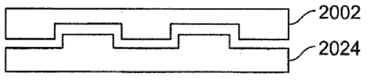
在一些实施方案中,光学堆叠16的所述层可被图案化成平行条带,且可形成显示装置中的行电极,如下文进一步描述。如所属领域的技术人员应理解,术语“图案化”在本文中用以指代掩盖以及蚀刻工艺。在一些实施方案中,例如铝(Al)的高导电和反射材料可用于可移动反射层14,且这些条带可形成显示装置中的列电极。可移动反射层14可形成为经沉积的金属层的一系列平行条带(正交于光学堆叠16的行电极),以形成沉积于柱18和沉积于柱18之间的介入牺牲材料的顶部上的若干列。当牺牲材料被蚀刻掉时,所界定间隙19或光学腔可在可移动反射层14与光学堆叠16之间形成。在一些实施方案中,柱18之间的间距可为约1μm到1000μm,而间隙19可为小于10,000埃
在一些实施方案中,每一IMOD像素(不管是处于经激活状态还是经松弛状态)基本上为由固定和移动反射层形成的电容器。当不施加电压时,可移动反射层14保持于机械上松弛的状态(如由图1中左侧的像素12所说明),其中间隙19处于可移动反射层14与光学堆叠16之间。然而,当将电位差(电压)施加到所选择的行和列中的至少一者时,在对应像素处于行电极与列电极的交叉点处所形成的电容器变得带电,且静电力将所述电极拉于一起。如果所施加电压超过阈值,则可移动反射层14可变形,且移动接近或抵靠光学堆叠16。光学堆叠16内的电介质层(未图示)可防止短接,且控制层14与层16之间的分离距离,如由图1中右侧的经激活像素12所说明。不管所施加的电位差的极性如何,表现皆为相同的。尽管在一些情况下,阵列中的一系列像素可被称作“行”或“列”,但所属领域的技术人员应容易理解,将一个方向称作“行”且另一方向称作“列”是任意的。重申,在一些定向中,行可被视为列,且列可被视为行。此外,显示元件可以正交的行与列(“阵列”)均匀地布置,或以非线性配置布置(例如,具有相对于彼此的某些位置偏移(“马赛克(mosaic)”))。术语“阵列”和“马赛克”可指代任一配置。因此,尽管显示器被称作包括“阵列”或“马赛克”,但在任何情况下,元件自身无需布置成正交于彼此,或以均匀分布来安置,但可包括具有不对称形状且不均匀分布的元件的布置。In some implementations, each IMOD pixel (whether in the actuated or relaxed state) is essentially a capacitor formed of fixed and moving reflective layers. When no voltage is applied, movable
图2展示说明并入有3×3干涉式调制器显示器的电子装置的系统方框图的实例。所述电子装置包括可经配置以执行一个或一个以上软件模块的处理器21。除了执行操作系统之外,处理器21还可经配置以执行一个或一个以上软件应用程序,包括网络浏览器、电话应用程序、电子邮件程序或任何其它软件应用程序。2 shows an example of a system block diagram illustrating an electronic device incorporating a 3x3 interferometric modulator display. The electronic device includes a
处理器21可经配置以与阵列驱动器22通信。阵列驱动器22可包括将信号提供到(例如)显示阵列或面板30的行驱动器电路24和列驱动器电路26。图1中所说明的IMOD显示装置的横截面是通过图2中的线1-1来展示。尽管为清晰起见,图2说明IMOD的3×3阵列,但显示阵列30可含有极大数目个IMOD,且可在行中具有与列中不同的IMOD的数目,且反之亦然。
图3展示说明图1的干涉式调制器的可移动反射层位置对所施加电压的图的实例。针对MEMS干涉式调制器,行/列(即,共同/片段)写入程序可利用这些装置的滞后性质,如图3中所说明。在一个实施方案中,干涉式调制器可能使用约10伏电位差,以致使可移动反射层或镜面从经松弛状态改变到经激活状态。当电压从那个值减小时,随着电压下降回低于10伏(在此实例中),可移动反射层维持其状态,然而,可移动反射层直到电压下降到低于2伏才完全松弛。因此,存在一电压范围(在此实例中,大约3伏到7伏),如图3中所示,其中存在所施加电压的窗,在所述窗内,装置稳定于经松弛状态或经激活状态。此窗在本文中被称作“滞后窗”或“稳定窗”。对于具有图3的滞后特性的显示阵列30而言,行/列写入程序可经设计成一次寻址一个或一个以上行,以使得在给定行的寻址期间,经寻址行中的待激活的像素暴露到约10伏(在此实例中)的电压差,且待松弛的像素暴露到接近零伏的电压差。在寻址之后,像素可暴露到稳定状态或大约5伏(在此实例中)的偏置电压差,以使得其保持于先前选通状态。在此实例中,在寻址之后,每一像素经历约3伏到7伏的“稳定窗”内的电位差。此滞后性质特征使得(例如)图1中所说明的像素设计图1能够在相同的所施加电压条件下保持稳定于经激活或经松弛的预先存在状态。由于每一IMOD像素(不管是处于经激活状态还是经松弛状态)基本上为由固定和移动反射层形成的电容器,所以此稳定状态可在滞后窗内的稳定电压下得以保持,而不会实质上消耗或损失电力。此外,如果所施加电压电位保持实质上固定,则基本上几乎无或无电流流入IMOD像素中。3 shows an example of a graph illustrating movable reflective layer position versus applied voltage for the interferometric modulator of FIG. 1 . For MEMS interferometric modulators, the row/column (ie common/segment) write procedure can take advantage of the hysteresis properties of these devices, as illustrated in FIG. 3 . In one implementation, an interferometric modulator may use a potential difference of about 10 volts to cause the movable reflective layer or mirror to change from a relaxed state to an actuated state. When the voltage is reduced from that value, the movable reflective layer maintains its state as the voltage drops back below 10 volts (in this example), however, the movable reflective layer does not fully relax until the voltage drops below 2 volts. Thus, there is a voltage range (in this example, about 3 volts to 7 volts), as shown in Figure 3, where there is a window of applied voltage within which the device is stable in the relaxed state or activated state. This window is referred to herein as the "hysteresis window" or "stability window". For a
在一些实施方案中,通过根据给定行中的像素的状态的所要改变(如果存在)沿着列电极集合施加呈“片段”电压的形式的数据信号,可产生图像的帧。可依次寻址阵列的每一行,以使得一次写入一行帧。为了将所要数据写入到第一行中的像素,可将对应于所述第一行中的像素的所要状态的片段电压施加于列电极上,且可将呈特定“共同”电压或信号的形式的第一行脉冲施加到第一行电极。可接着将片段电压的集合改变成对应于第二行中的像素的状态的所要改变(如果存在),且可将第二共同电压施加到第二行电极。在一些实施方案中,第一行中的像素不受沿着列电极所施加的片段电压的改变影响,且保持于其在第一共同电压行脉冲期间被设定到的状态。可以循序的方式对整个系列的行或者列重复此过程,以产生图像帧。可通过以每秒某所要数目个帧连续地重复此过程而用新的图像数据刷新和/或更新所述帧。In some implementations, a frame of an image may be produced by applying a data signal in the form of a "segment" voltage along a set of column electrodes according to the desired change in state of the pixels in a given row, if any. Each row of the array can be addressed in turn, such that one row of frames is written at a time. To write the desired data to the pixels in the first row, a segment voltage corresponding to the desired state of the pixels in the first row may be applied to the column electrodes, and a specific "common" voltage or signal may be applied to the form the first row pulse applied to the first row electrode. The set of segment voltages can then be changed to correspond to the desired change of state of the pixels in the second row, if any, and a second common voltage can be applied to the second row electrode. In some implementations, the pixels in the first row are unaffected by changes in the segment voltage applied along the column electrodes, and remain in the state they were set to during the first common voltage row pulse. This process can be repeated in a sequential fashion for the entire series of rows or columns to produce image frames. The frames may be refreshed and/or updated with new image data by continuously repeating this process at some desired number of frames per second.
跨越每一像素所施加的片段和共同信号的组合(即,跨越每一像素的电位差)确定每一像素的所得状态。图4展示说明在施加各种共同电压和片段电压时干涉式调制器的各种状态的表的实例。如所属领域的技术人员应理解,可将“片段”电压施加到列电极或行电极,且可将“共同”电压施加到列电极或行电极中的另一者。The combination of the segment and common signals applied across each pixel (ie, the potential difference across each pixel) determines the resulting state of each pixel. 4 shows an example of a table illustrating various states of an interferometric modulator when various common and segment voltages are applied. As will be understood by those skilled in the art, a "segment" voltage may be applied to either the column or row electrodes, and a "common" voltage may be applied to the other of the column or row electrodes.
如图4中(以及图5B中所展示的时序图中)所说明,当沿着共同线施加释放电压VCREL时,沿着所述共同线的所有干涉式调制器元件将置于经松弛状态(或者被称作释放或未激活状态),而不管沿着片段线所施加的电压(即,高片段电压VSH和低片段电压VSL)如何。具体来说,当沿着共同线施加释放电压VCREL时,在沿着像素的对应片段线施加高片段电压VSH和低片段电压VSL两者时,跨越调制器像素的电位电压(或者被称作像素电压)处于松弛窗(参看图3,还被称作释放窗)内。As illustrated in FIG. 4 (and the timing diagram shown in FIG. 5B ), when the release voltage V REL is applied along a common line, all interferometric modulator elements along that common line will be placed in a relaxed state (Alternatively referred to as a released or inactive state), regardless of the voltages applied along the segment lines (ie, high segment voltage VSH and low segment voltage VSL ). Specifically, when the release voltage VC REL is applied along the common line, when both the high segment voltage VSH and the low segment voltage VSL are applied along the pixel's corresponding segment line, the potential voltage across the modulator pixel (or is referred to as the pixel voltage) is within the relaxation window (see FIG. 3, also referred to as the release window).
当将保持电压施加于共同线上(例如,高保持电压VCHOLD_H或低保持电压VCHOLD_L)时,干涉式调制器的状态将保持恒定。举例来说,经松弛IMOD将保持于经松弛位置,且经激活IMOD将保持于经激活位置。可选择保持电压,以使得在沿着对应片段线施加高片段电压VSH和低片段电压VSL两者时,像素电压将保持在稳定窗内。因此,片段电压摆动(即,高VSH与低片段电压VSL之间的差)小于正稳定窗或负稳定窗的宽度。When a hold voltage is applied on the common line (eg, high hold voltage VC HOLD_H or low hold voltage VC HOLD_L ), the state of the interferometric modulator will remain constant. For example, a relaxed IMOD will remain in the relaxed position, and an activated IMOD will remain in the activated position. The hold voltages can be selected such that the pixel voltage will remain within a stability window when both the high segment voltage VSH and the low segment voltage VSL are applied along the corresponding segment line. Therefore, the segment voltage swing (ie, the difference between the high VSH and low segment voltage VSL ) is smaller than the width of the positive or negative stability windows.
当将寻址或激活电压施加于共同线上(例如,高寻址电压VCADD_H或低寻址电压VCADD_L)时,可通过沿着相应片段线施加片段电压而沿着所述共同线将数据选择性地写入到调制器。可选择片段电压,以使得激活取决于所施加的片段电压。当沿着共同线施加寻址电压时,施加片段电压将产生处于稳定窗内的像素电压,从而致使所述像素保持未激活。相比而言,施加另一片段电压将产生在稳定窗外的像素电压,从而导致所述像素的激活。引起激活的特定片段电压可视使用哪一寻址电压而变化。在一些实施方案中,当沿着共同线施加高寻址电压VCADD_H时,施加高片段电压VSH可致使调制器保持于其当前位置,而施加低片段电压VSL可引起调制器的激活。作为推论,当施加低寻址电压VCADD_L时,片段电压的效应可为相反的,其中高片段电压VSH引起调制器的激活,且低片段电压VSL对调制器的状态无影响(即,保持稳定)。When addressing or activation voltages are applied to a common line (e.g., high addressing voltage VC ADD_H or low addressing voltage VC ADD_L ), data can be transferred along the corresponding segment line by applying segment voltages along the common line. selectively written to the modulator. Segment voltages can be selected such that activation is dependent on the applied segment voltage. When the addressing voltage is applied along the common line, applying the segment voltage will result in a pixel voltage within the stability window, causing the pixel to remain inactive. In contrast, applying another segment voltage will result in a pixel voltage outside the stability window, resulting in actuation of the pixel. The particular segment voltage that causes activation can vary depending on which addressing voltage is used. In some implementations, when the high addressing voltage VC ADD_H is applied along the common line, applying the high segment voltage VSH can cause the modulator to remain in its current position, while applying the low segment voltage VSL can cause activation of the modulator. As a corollary, the effect of the segment voltage may be reversed when a low addressing voltage VC ADD_L is applied, where a high segment voltage VSH causes activation of the modulator and a low segment voltage VSL has no effect on the state of the modulator (i.e., keep it steady).
在一些实施方案中,可使用产生跨越调制器的相同极性电位差的保持电压、地址电压和片段电压。在一些其它实施方案中,可使用不时地使调制器的电位差的极性交替的信号。跨越调制器的极性的交替(即,写入程序的极性的交替)可减小或抑制可在单一极性的重复的写入操作之后发生的电荷累积。In some implementations, hold, address, and segment voltages may be used that produce the same polarity potential difference across the modulator. In some other implementations, a signal that alternates the polarity of the modulator's potential difference from time to time may be used. The alternation of polarities across the modulator (ie, the alternation of the polarity of the write program) can reduce or suppress charge accumulation that can occur after repeated write operations of a single polarity.
图5A展示说明图2的3×3干涉式调制器显示器中的显示数据的帧的图的实例。图5B展示可用以写入图5A中所说明的显示数据的帧的共同信号和片段信号的时序图的实例。可将信号施加到类似于图2的阵列的3×3阵列,此将最终产生图5A中所说明的线时间60e显示布置。图5A中的经激活调制器处于黑暗状态,即,其中大部分的反射光在可见光谱外以对(例如)观看者产生黑暗外观。在写入图5A中所说明的帧之前,像素可处于任何状态,但图5B的时序图中所说明的写入程序假定:在第一线时间60a之前,每一调制器已被释放且驻留于未激活状态中。5A shows an example of a diagram illustrating a frame of display data in the 3x3 interferometric modulator display of FIG. 2 . 5B shows an example of a timing diagram of common and segment signals that may be used to write a frame of display data illustrated in FIG. 5A. The signal can be applied to a 3x3 array similar to that of Figure 2, which will ultimately result in the line time 60e display arrangement illustrated in Figure 5A. The activated modulator in FIG. 5A is in the dark state, ie, where most of the reflected light is outside the visible spectrum to create a dark appearance, for example, to a viewer. The pixels may be in any state prior to writing the frame illustrated in Figure 5A, but the write procedure illustrated in the timing diagram of Figure 5B assumes that each modulator has been released and parked prior to the first line time 60a. Leave in an inactive state.
在第一线时间60a期间:将释放电压70施加于共同线1上;施加于共同线2上的电压在高保持电压72处开始且移动到释放电压70;且沿着共同线3施加低保持电压76。因此,沿着共同线1的调制器(共同1,片段1)(1,2)和(1,3)保持于经松弛或未激活状态并持续第一线时间60a的持续时间,沿着共同线2的调制器(2,1)、(2,2)和(2,3)将移动到经松弛状态,且沿着共同线3的调制器(3,1)、(3,2)和(3,3)将保持于其先前状态。参看图4,沿着片段线1、2和3所施加的片段电压将对干涉式调制器的状态无影响,因为共同线1、2或3均未正暴露到在线时间60a期间引起激活的电压电平(即,VCREL-松弛和VCHoLD_L-稳定)。During first line time 60a: release voltage 70 is applied on
在第二线时间60b期间,共同线1上的电压移动到高保持电压72,且沿着共同线1的所有调制器保持于经松弛状态,而不管所施加的片段电压如何,因为无寻址或激活电压施加于共同线1上。沿着共同线2的调制器归因于施加释放电压70而保持于经松弛状态,且当沿着共同线3的电压移动到释放电压70时,沿着共同线3的调制器(3,1)、(3,2)和(3,3)将松弛。During the second line time 60b, the voltage on
在第三线时间60c期间,通过将高地址电压74施加于共同线1上来寻址共同线1。因为在施加此地址电压期间沿着片段线1和2施加低片段电压64,所以跨越调制器(1,1)和(1,2)的像素电压大于所述调制器的正稳定窗的高端(即,电压微分超过预定义阈值),且激活调制器(1,1)和(1,2)。相反地,因为沿着片段线3施加高片段电压62,所以跨越调制器(1,3)的像素电压小于调制器(1,1)和(1,2)的像素电压,且保持在所述调制器的正稳定窗内;调制器(1,3)因此保持松弛。而且,在线时间60c期间,沿着共同线2的电压减小到低保持电压76,且沿着共同线3的电压保持于释放电压70,从而使得沿着共同线2和3的调制器保持处于经松弛位置。During third line time 60c,
在第四线时间60d期间,共同线1上的电压返回到高保持电压72,从而使得沿着共同线1的调制器保持处于其相应经寻址状态。共同线2上的电压减小到低地址电压78。因为沿着片段线2施加高片段电压62,所以跨越调制器(2,2)的像素电压低于所述调制器的负稳定窗的下端,从而引起所述调制器(2,2)激活。相反地,因为沿着片段线1和3施加低片段电压64,所以调制器(2,1)和(2,3)保持于经松弛位置。共同线3上的电压增大到高保持电压72,从而使得沿着共同线3的调制器保持处于经松弛状态。During the fourth line time 6Od, the voltage on
最后,在第五线时间60e期间,共同线1上的电压保持于高保持电压72,且共同线2上的电压保持于低保持电压76,从而使得沿着共同线1和2的调制器处于其相应经寻址状态。共同线3上的电压增大到高地址电压74,以沿着共同线3寻址调制器。随着将低片段电压64施加于片段线2和3上,调制器(3,2)和(3,3)激活,而沿着片段线1所施加的高片段电压62使得调制器(3,1)保持于经松弛位置。因此,在第五线时间60e的末尾,3×3像素阵列处于图5A中所展示的状态,且只要沿着共同线施加保持电压,则所述3×3像素阵列将保持于那个状态,而不管在沿着其它共同线(未图示)的调制器正被寻址时可能发生的片段电压的变化如何。Finally, during fifth line time 60e, the voltage on
在图5B的时序图中,给定的写入程序(即,线时间60a到60e)可包括高保持电压和地址电压或低保持电压和地址电压的使用。一旦已针对给定的共同线完成写入程序(且将共同电压设定到具有与激活电压相同的极性的保持电压),则像素电压保持在给定的稳定窗内,且直到释放电压被施加于那个共同线上才通过松弛窗。此外,由于在寻址每一调制器之前释放所述调制器作为写入程序的部分,所以调制器的激活时间(而非释放时间)可确定线时间。特定来说,在调制器的释放时间大于激活时间的实施方案中,与单一线时间相比,可更长久地施加释放电压,如图5B中所描绘。在一些其它实施方案中,沿着共同线或片段线所施加的电压可变化,以考虑不同调制器(例如,具有不同色彩的调制器)的激活电压和释放电压的变化。In the timing diagram of FIG. 5B, a given write procedure (ie, line times 60a through 60e) may include the use of either a high hold voltage and an address voltage or a low hold voltage and an address voltage. Once the write procedure has been completed for a given common line (and the common voltage is set to a hold voltage with the same polarity as the actuation voltage), the pixel voltage remains within a given stability window until the release voltage is applied to that common line only through the slack window. Furthermore, since each modulator is released as part of the write procedure before it is addressed, the actuation time of the modulators (rather than the release time) may determine the line time. In particular, in implementations where the release time of the modulator is greater than the actuation time, the release voltage can be applied longer than a single line time, as depicted in Figure 5B. In some other implementations, the voltages applied along the common or segment lines can vary to account for variations in the actuation and release voltages of different modulators (eg, modulators with different colors).
根据上文所阐述的原理而操作的干涉式调制器的结构的细节可广泛变化。举例来说,图6A到6E展示干涉式调制器的不同实施方案的横截面的实例,所述干涉式调制器包括可移动反射层14和其支撑结构。图6A展示图1的干涉式调制器显示器的部分横截面的实例,其中金属材料条带(即,可移动反射层14)沉积于从衬底20正交地延伸的支撑件18上。在图6B中,每一IMOD的可移动反射层14的形状一般为正方形或矩形,且在系链32上在隅角处或附近附接到支撑件。在图5C中,可移动反射层14的形状一般为正方形或矩形,且从可包括柔性金属的可变形层34悬置。可变形层34可在可移动反射层14的周边周围直接或间接地连接到衬底20。这些连接件在本文中被称作支撑柱。图6C中所展示的实施方案具有得自将可移动反射层14的光学功能与其机械功能去耦的额外益处,所述去耦由可变形层34执行。此去耦允许用于反射层14的结构设计和材料和用于可变形层34的结构设计和材料独立于彼此而优化。The details of the structure of interferometric modulators operating according to the principles set forth above may vary widely. For example, Figures 6A-6E show examples of cross-sections of different implementations of interferometric modulators including the movable
图6D展示IMOD的另一实例,其中可移动反射层14包括反射子层14a。可移动反射层14搁置于例如支撑柱18等支撑结构上。支撑柱18提供可移动反射层14与下部固定电极(即,所说明的IMOD中的光学堆叠16的部分)的分离,使得(例如)在可移动反射层14处于经松弛位置时,间隙19形成于可移动反射层14与光学堆叠16之间。可移动反射层14还可包括可经配置以充当电极的导电层14c和支撑层14b。在此实例中,导电层14c安置于支撑层14b的远离衬底20的一侧上,且反射子层14a安置于支撑层14b的接近衬底20的另一侧上。在一些实施方案中,反射子层14a可为导电的,且可安置于支撑层14b与光学堆叠16之间。支撑层14b可包括一个或一个以上电介质材料(例如,氮氧化硅(SiON)或二氧化硅(SiO2))层。在一些实施方案中,支撑层14b可为若干层的堆叠,例如SiO2/SiON/SiO2三层堆叠。反射子层14a和导电层14c中的任一者或两者可包括(例如)具有约0.5%的铜(Cu)的铝(Al)合金,或另一反射金属材料。在电介质支撑层14b上方使用导电层14c且电介质支撑层14b下方使用导电层14a可平衡应力且提供增强的导电。在一些实施方案中,反射子层14a和导电层14c可由不同材料形成,以实现多种设计目的,例如实现可移动反射层14内的特定应力轮廓。Figure 6D shows another example of an IMOD in which the movable
如图6D中所说明,一些实施方案还可包括黑色掩模结构23。黑色掩模结构23可形成在光学上非作用区中(例如,像素之间或柱18下方),以吸收环境光或杂散光。黑色掩模结构23还可通过抑制光从显示器的非作用部分反射或透射通过显示器的非作用部分而改进显示装置的光学性质,借此增大对比率。另外,黑色掩模结构23可为导电的,且经配置以充当电总线传输(bussing)层。在一些实施方案中,行电极可连接到黑色掩模结构23,以减小所连接的行电极的电阻。可使用包括沉积技术和图案化技术在内的多种方法来形成黑色掩模结构23。黑色掩模结构23可包括一个或一个以上层。举例来说,在一些实施方案中,黑色掩模结构23包括充当光学吸收体的钼铬(MoCr)层、层,和充当反射体和总线传输层的铝合金,其厚度分别在约

图6E展示IMOD的另一实例,其中可移动反射层14为自支撑的。与图6D对比,图6E的实施方案不包括支撑柱18。而是,可移动反射层14在多个位置处接触下伏光学堆叠16,且可移动反射层14的曲率提供足够支撑,使得在跨越干涉式调制器的电压不足以引起激活时,可移动反射层14返回到图6E的未激活位置。为清晰起见,此处将可含有多个若干不同层的光学堆叠16展示为包括光学吸收体16a和电介质16b。在一些实施方案中,光学吸收体16a可充当固定电极和部分反射层两者。Figure 6E shows another example of an IMOD in which the movable
在例如图6A到6E中所展示的那些实施方案的实施方案中,IMOD充当直观式装置,其中从透明衬底20的前侧(即,与其上形成有调制器的侧相对的侧)观看图像。在这些实施方案中,装置的背面部分(即,显示装置的在可移动反射层14后方的任何部分,其包括(例如)图6C中所说明的可变形层34)可经配置,且可对其进行操作,而不会冲击或不利地影响显示装置的图像质量,因为反射层14以光学方式遮蔽装置的那些部分。举例来说,在一些实施方案中,可在可移动反射层14后方包括总线结构(未说明),其提供将调制器的光学性质与调制器的机电性质分离的能力(例如,电压寻址和由此寻址引起的移动)。另外,图6A到6E的实施方案可简化例如图案化等处理。In embodiments such as those shown in FIGS. 6A-6E , the IMOD acts as a direct-view device, where the image is viewed from the front side of the transparent substrate 20 (i.e., the side opposite the side on which the modulator is formed). . In these implementations, the backside portion of the device (i.e., any portion of the display device behind the movable
图7展示说明干涉式调制器的制造工艺80的流程图的实例,且图8A到8E展示此制造工艺80的对应阶段的横截面示意说明的实例。在一些实施方案中,可实施制造工艺80以制造机电系统装置,例如图1和6中所说明的一般类型的干涉式调制器。机电系统装置的制造还可包括图7中未展示的其它块。参看图1、6和7,工艺80从在衬底20上形成光学堆叠16的块82开始。图8A说明形成于衬底20上的此光学堆叠16。衬底20可为例如玻璃或塑料等透明衬底,其可为柔性的或相对硬且不弯曲的,且可能已经受之前的制备工艺(例如,清洁)以促进有效地形成光学堆叠16。如上文所论述,光学堆叠16可为导电的,部分透明且部分反射的,且可(例如)通过将具有所要性质的一个或一个以上层沉积到透明衬底20上而制造。在图8A中,光学堆叠16包括具有子层16a和16b的多层结构,但更多或更少的子层可包括于一些其它实施方案中。在一些实施方案中,子层16a和16b中的一者可配置有光学吸收性质和导电性质两者,例如组合式导体/吸收体子层16a。另外,子层16a和16b中的一者或一者以上可被图案化成平行条带,且可形成显示装置中的行电极。可通过掩盖和蚀刻工艺或此项技术中已知的另一合适工艺来执行此图案化。在一些实施方案中,子层16a和16b中的一者可为绝缘层或电介质层,例如沉积于一个或一个以上金属层(例如,一个或一个以上反射层和/或导电层)上的子层16b。另外,光学堆叠16可被图案化成形成显示器的行的个别且平行的条带。请注意,图8A到8E可不按比例绘制。举例来说,在一些实施方案中,光学堆叠的子层中的一者、光学吸收层可非常薄,但子层16a和16b在图8A到8E中展示为有点厚。FIG. 7 shows an example of a flow diagram illustrating a
工艺80在块84处以在光学堆叠16上形成牺牲层25而继续。稍后移除牺牲层25(例如,在块90处)以形成腔19,且因此,未在图1中所说明的所得干涉式调制器12中展示牺牲层25。图8B说明包括形成于光学堆叠16上的牺牲层25的经部分制造的装置。在光学堆叠16上形成牺牲层25可包括:以在后续移除之后提供具有所要大小的间隙或腔19(还参看图1和8E)而选择的厚度来沉积例如钼(Mo)或非晶硅(a-Si)等二氟化氙(XeF2)可蚀刻材料。可使用例如物理气相沉积(PVD,例如,溅镀)、等离子体增强型化学气相沉积(PECVD)、热化学气相沉积(热CVD)或旋涂等沉积技术来执行牺牲材料的沉积。
工艺80在块86处以形成支撑结构(例如,图1、6和8C中所说明的柱18)而继续。形成柱18可包括将牺牲层25图案化以形成支撑结构孔隙,接着使用例如PVD、PECVD、热CVD或旋涂等沉积方法将材料(例如,聚合物或无机材料(例如,氧化硅))沉积到所述孔隙中以形成柱18。在一些实施方案中,形成于牺牲层中的支撑结构孔隙可通过牺牲层25与光学堆叠16两者而延伸到下伏衬底20,使得柱18的下端接触衬底20,如图6A中所说明。或者,如图8C中所描绘,形成于牺牲层25中的孔隙可延伸通过牺牲层25,但不通过光学堆叠16。举例来说,图8E说明支撑柱18的下端与光学堆叠16的上表面接触。通过将支撑结构材料层沉积于牺牲层25上且将远离牺牲层25中的孔隙而定位的支撑结构材料的多个部分图案化,可形成柱18或其它支撑结构。支撑结构可位于孔隙内(如图8C中所说明),但还可至少部分地在牺牲层25的一部分上延伸。如上文所述,牺牲层25和/或支撑柱18的图案化可通过图案化和蚀刻工艺来执行,但还可通过替代性蚀刻方法来执行。
工艺80在块88处以形成可移动反射层或薄膜(例如,图1、6和8D中所说明的可移动反射层14)而继续。可通过使用一个或一个以上沉积步骤(包含(例如)反射层(例如,铝、铝合金或其它反射层)沉积)连同一个或一个以上图案化、掩盖和/或蚀刻步骤来形成可移动反射层14。可移动反射层14可为导电的,且被称作导电层。在一些实施方案中,可移动反射层14可包括多个子层14a、14b和14c,如图8D中所展示。在一些实施方案中,所述子层中的一者或一者以上(例如,子层14a和14c)可包括针对其光学性质所选择的高反射子层,且另一子层14b可包括针对其机械性质所选择的机械子层。由于牺牲层25仍存在于在块88处所形成的经部分制造的干涉式调制器中,所以可移动反射层14通常在此阶段不可移动。含有牺牲层25的经部分制造的IMOD还可在本文中被称作“未释放的”IMOD。如上文结合图1所描述,可将可移动反射层14图案化成形成显示器的列的个别且平行的条带。
工艺80在块90处以形成腔(例如,如图1、6和8E中所说明的腔19)而继续。可通过将牺牲材料25(在块84处所沉积)暴露到蚀刻剂而形成腔19。举例来说,可(例如)通过将牺牲层25暴露到气体或蒸气蚀刻剂(例如,从固态XeF2得到的蒸气)并持续对移除所要量的材料(通常相对于围绕腔19的结构而选择性地移除)为有效的时间周期,通过干式化学蚀刻来移除例如Mo或非晶Si等可蚀刻牺牲材料。还可使用例如湿式蚀刻和/或等离子体蚀刻等其它蚀刻方法。由于在块90期间移除牺牲层25,所以可移动反射层14通常可在此阶段之后移动。在移除牺牲材料25之后,所得的经完全或部分制造的IMOD可在本文中被称作“经释放的”IMOD。
上文所描述的干涉式调制器为具有两个状态:松弛状态和激活状态的双稳态显示元件。以下描述涉及模拟干涉式调制器。举例来说,在模拟干涉式调制器的一个实施方案中,单一干涉式调制器可反射红色、绿色、蓝色、黑色和白色。在一些实施方案中,模拟干涉式调制器可取决于所施加电压而反射光的波长范围内的任何色彩。此外,模拟干涉式调制器的光学堆叠可不同于上文所描述的双稳态显示元件。这些差异可产生不同光学结果。举例来说,在上述的双稳态组件的一些实施方案中,闭合(激活)状态给予双稳态元件黑暗(例如,黑色)反射状态。在一些实施方案中,模拟干涉式调制器在电极处于类似于双稳态元件的闭合状态的位置中时反射白光。The interferometric modulators described above are bistable display elements with two states: a relaxed state and an actuated state. The following description refers to analog interferometric modulators. For example, in one implementation of an analog interferometric modulator, a single interferometric modulator can reflect red, green, blue, black, and white. In some implementations, an analog interferometric modulator can reflect any color within the wavelength range of light depending on the applied voltage. Furthermore, the optical stack of the analog interferometric modulators can be different than the bistable display elements described above. These differences can produce different optical results. For example, in some embodiments of the bistable components described above, the closed (activated) state imparts a dark (eg, black) reflective state to the bistable element. In some implementations, the analog interferometric modulator reflects white light when the electrodes are in a position similar to the closed state of the bistable element.
三端子机电装置(例如,干涉式调制器)可包括安置于上部电极和下部电极之间的间隙中的可移动中间电极。在一种方法中,三端子装置可使用开关或串联电容器将电荷提供到所述中间电极上。接着,可跨越所述上部电极和所述下部电极施加电压,且所述带电中间电极可与产生于所述上部电极与所述下部电极之间的所得电场相互作用。结果,所述带电中间电极可基于由所施加电压产生的电场移动或移位。然而,以此方式使用开关和电容器将电荷提供到所述中间电极可导致所述中间电极的寄生负载。虽然所述方式可用以将电荷提供到未电连接到任何外部电路且因此被电隔离的电荷中性中间电极上,但电荷中性中间电极一般可不响应所述上部电极与所述下部电极之间的所施加电场。因此,以下装置和方法可为有用的:使具有零净电荷的被电隔离中间电极移动,使得所述中间电极接触电触点(或电极),借此将电荷赋予所述中间电极。用以在中间电极接收电荷之后释放所述中间电极的装置和方法也可为有用的。A three-terminal electromechanical device (eg, an interferometric modulator) may include a movable middle electrode disposed in a gap between an upper electrode and a lower electrode. In one approach, a three terminal device may use a switch or a series capacitor to provide charge onto the middle electrode. A voltage can then be applied across the upper and lower electrodes, and the charged middle electrode can interact with the resulting electric field generated between the upper and lower electrodes. As a result, the charged middle electrode can move or be displaced based on the electric field generated by the applied voltage. However, using switches and capacitors to provide charge to the middle electrode in this manner can result in parasitic loading of the middle electrode. While the approach described can be used to provide charge to a charge-neutral middle electrode that is not electrically connected to any external circuitry and is therefore electrically isolated, the charge-neutral middle electrode generally may not respond to a gap between the upper electrode and the lower electrode. of the applied electric field. Accordingly, devices and methods may be useful for moving an electrically isolated middle electrode having zero net charge such that the middle electrode contacts an electrical contact (or electrode), thereby imparting charge to the middle electrode. Devices and methods to release an intermediate electrode after it has received a charge may also be useful.
图9展示说明用于激活和校准模拟干涉式调制器的电荷中性电极的一种方法的流程图的实例。方法900从块951开始,在所述块中,提供被电隔离的电荷中性中间电极。举例来说,在带电和/或校准之前、当装置第一次通电时或在电荷已由于泄漏或有目的的电荷耗散程序耗尽之后,所述被电隔离中间电极可为电荷中性的。所述方法在块952处继续,在所述块中,激活所述中间电极,从而使用电力使所述中间电极朝向另一电极移动。以下(例如)参看图12到20描述用以在所述中间电极为电荷中性时激活所述中间电极的装置和方法。方法900在块953处继续,在所述块中,将电荷提供到所述中间电极。图21到25描述用于将电荷置于此中间电极上的系统和方法的一些一般实施方案。具体来说,参看图21到23描述用于通过与上部电极接触而对中间电极进行充电的装置和方法,且参看图22以及图24到25描述用于通过与被隔离的接地互补电极接触而对中间电极进行充电的装置和方法。在一些实施方案中,如参看图26到30所描述,可使用开关配置对电荷中性中间电极进行充电,而在其它实施方案中,如参看图34到38所描述,可使用无开关配置对所述中间电极进行充电。9 shows an example of a flowchart illustrating one method for activating and calibrating charge-neutral electrodes of an analog interferometric modulator.
方法900包括块954,在所述块中,校准置于中间电极上的电荷以考虑到作用于中间电极的特定机械弹簧力。参看图31到33描述用于使用开关配置校准电荷的特定装置和方法。另外,参看图39到41描述用于使用无开关配置校准电荷的装置和方法的一些实施方案。校准三端子装置的阵列上的具有所要量的电荷的中间电极中的每一者可允许所有所述中间电极在跨越所有所述装置施加选定电压之后即刻可靠地向相同位置移动。此可帮助改进显示于模拟干涉式调制器显示器中的色彩的准确度。
方法900在块955处继续,在所述块中,操作包括具有经校准中间电极的模拟干涉式调制器的阵列的显示器。在一些方面中,操作显示器包括激活中间电极或使所述中间电极移动到由上部电极1002和下部电极1010(参见图10)形成的间隙中的各个位置以显示图像。中间电极的位置帮助确定模拟干涉式调制器像素的反射显示色彩。方法900任选地在块956处继续,在所述块中,重复块952到955。在一些实施方案中,在返回块952之前,使中间电极为电荷中性的。在一些实施方案中,中间电极在其于块952处激活时保持一些电荷。
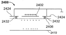
图10展示具有三层或电极设计的模拟干涉式调制器1000的横截面的实例。调制器1000包括上部或第一电极1002。在一个实施方案中,电极1002为由金属制成的板。上部电极1002可使用加强层1003加强。在一个实施方案中,加强层1003为电介质。加强层1003可用以使上部电极1002保持刚性且实质上平坦。调制器900还包括下部或第二电极1010,和也可包括金属的中间或第三电极1006。所述三个电极通过绝缘柱1004电绝缘。绝缘柱1004还用来在不存在电力时将中间电极1006在平衡位置中固持在电极1002与1010之间。中间电极1006具有安置于其上的加强层1008。在一个实施方案中,加强层1008包括氮氧化硅。FIG. 10 shows an example of a cross-section of an
中间电极1006经配置以在上部电极1002与下部电极1010之间的区域或间隙中移动。加强层1008帮助当中间电极1006在电极1002与1010之间移动时使中间电极1006的一部分保持相对刚性且平坦。在一个实施方案中,加强层1008安置于中间电极1006的中心部分上。在此实施方案中,中间电极1006的侧部能够在中间电极1006移动时弯曲。在图10中,展示处于平衡位置中的中间电极1006,所述电极在所述平衡位置中实质上平坦。当中间电极1006移动远离此平衡位置时,中间电极1006的侧部将变形或弯曲。中间电极1006的侧部实施弹性弹簧力,所述弹性弹簧力施加力以使中间电极1006移动回到所述平衡位置(参见(例如)图26到33中的弹簧2634和图34到41中的弹簧3434)。The
中间电极1006还充当用以反射穿过衬底1012进入结构的光的镜。在一些实施方案中,衬底1012由玻璃制成。在一个实施方案中,下部电极1010为吸收铬或含铬的层。为了保持至少部分透明,可使所述吸收层相对薄,如上所述。下部电极1010具有安置于其上的钝化层1014(现具体展示为单独层)。在一个实施方案中,钝化层1014为薄电介质层。在另一实施方案中,上部电极1002具有安置于其上的钝化层。在一些实施方案中,所述钝化层为薄电介质层。The
图11A展示具有控制电路1120的模拟干涉式调制器1100的横截面的实例。模拟干涉式调制器1100可为调制器1000或其它类似设计的模拟干涉式调制器。调制器1100包括上部电极1102、中间电极1106和下部电极1110。调制器1100进一步包括使电极1102、1106和1110与其它结构绝缘的绝缘柱1104。调制器1100进一步包括安置于上部电极1102上的电阻性元件1116。上部电极1102具有安置于其上的加强层1103。在一个实施方案中,上部电极1102为金属,且加强层1103为电介质。调制器1100还包括安置于下部电极1110上的薄的电介质钝化层1114,以使得电介质钝化层1114安置于下部电极1110与中间电极1106之间。下部电极1110安置于衬底1112上。电阻性元件1116提供上部电极1102与中间电极1106之间的隔离物。当中间电极1106朝向上部电极1102移动时,电阻性元件1116防止中间电极1106与上部电极1102接触。在一个实施方案中,中间电极1106包括安置于中间电极1106的底部部分上的绝缘层(未图示)。11A shows an example of a cross-section of an
模拟干涉式调制器1100还包括控制电路1120。控制电路1120经配置以跨越上部电极1102和下部电极1110施加电压。电荷泵电路1118经配置以将电荷选择性地施加到中间电极1106。通过使用控制电压1120和电荷泵电路1118,实现中间电极1106的激活。电荷泵电路1118用以为中间电极1106提供电荷。带电中间电极1106接着与由控制电路1120在上部电极1102与下部电极1110之间产生的电场相互作用。带电中间电极1106与所述电场的相互作用使中间电极1106在电极1102与1110之间移动。The
在图11B的示意图中说明可实施为用以将准确量的电荷置于IMOD上的电荷泵电路1118的电荷注入电路的一个实例。在这些示意图中,将IMOD描绘为可变电容器。复位IMOD(左边)示意图说明用于复位IMOD的实例电路配置。在此配置中,开关S3闭合,从而使IMOD短路以耗散IMOD上的电荷。开关S1和S2“断开”,从而使电压源Vin和电容器Cin相互隔离且与IMOD隔离。预充电Cin(在中央)示意图说明开关S1闭合从而将电压源Vin连接到电容器Cin、使电容器Cin带电的实例电路配置。开关S2断开,从而隔离电容器Cin与IMOD,且开关S3断开,使得IMOD不再短路。在对电荷进行取样且将电荷转移到IMOD(右边)示意图中,开关S1断开,从而隔离电压源Vin与所述电路的其余部分,且开关S2闭合,从而将电容器Cin连接到运算放大器的虚拟接地输入,所述虚拟接地输入保持连接到IMOD端子1(左端子)。运算放大器输出以反馈方式连接到IMOD的端子2。此为众所周知的切换电容器电路,其准确地将电荷从输入电容器Cin转移到反馈路径中的电容器(在此情况下为IMOD)。可使用无运算放大器的开关实施导致不完全电荷转移的其它方法。One example of a charge injection circuit that may be implemented as a
通过改变由控制电路1120施加的电压可使中间电极1106移动到电极1102与1110之间的各种位置。举例来说,由控制电路1120施加的正电压Vc使下部电极1110相对于上部电极1102被驱动到正电位,如果中间电极1106带正电,则下部电极1110排斥所述中间电极1106。因此,正电压Vc使中间电极1106朝向上部电极1102移动。由控制电路1120施加负电压Vc致使下部电极1110相对于上部电极1102被驱动到负电位,当中间电极1106带正电时,下部电极1110吸引中间电极1106。因此,负电压Vc致使中间电极1106朝向下部电极1110移动。
开关1122可用以选择性地连接或断开中间电极1106与电荷泵电路1118。可使用此项技术中已知的除开关之外的其它方法来选择性地连接或断开中间电极1106与电荷泵电路1118,例如薄膜半导体、熔丝、反熔丝等。The
可配置模拟干涉式调制器1100,以使得中间电极1106以与跨越上部电极1102和下部电极1110驱动的电压成线性比例的方式响应。因此,用以控制中间电极1106的移动的电压与中间电极1106在电极1102与1110之间的位置之间存在线性关系。The
使用开关1122将电荷提供到中间电极1106可导致中间电极1106的寄生负载。举例来说,如果中间电极1106未完全被电隔离,则中间电极1106上的存储电荷Q可随中间电极在电极1102与1110之间的位置而变化。Q的此变化可影响中间电极1106对电荷的响应。当中间电极1106未完全被电隔离时,存在从中间电极附接到上部电极1102和下部电极1110中的每一者的寄生电容。另外,存储电荷Q的一部分可随时间而经由开关1122从中间电极1106泄漏。Providing charge to
可使用各种系统和方法来考虑寄生电容,例如2011年8月2日颁布的题为“模拟干涉式调制器(Analog Interferometric Modulator)”的第7,990,604号美国专利中所描述的系统和方法。举例来说,调制器1100可经配置以通过包括与中间电极1106串联连接且与寄生电容1140和1142并联连接的电容器来考虑寄生电容。因此在无中间电极1106到开关或串联电容器的电连接的情况下将电荷提供于中间电极1106上、接着隔离所述电荷可为有利的。此被电隔离的电极可减小寄生负载或电荷泄漏问题。Various systems and methods can be used to account for parasitic capacitance, such as those described in US Patent No. 7,990,604, issued August 2, 2011, entitled "Analog Interferometric Modulator." For example,
激活中性的被电隔离电极Activate neutral electrically isolated electrodes
图12展示模拟干涉式调制器1200的透视图的实例,模拟干涉式调制器1200包括中间电极,所述中间电极可在不使用电连接到所述中间电极的开关或串联电容器的情况下在两个带电电极之间移动或激活。如下文参看图21到23更详细地描述,可使中间电极朝向任一带电电极移动以在不使用电连接到中间电极的开关或串联电容器的情况下将电荷提供到中间电极上。12 shows an example of a perspective view of an
调制器1200包括与上部电极1202间隔开恒定间隙g的上部电极1202和下部电极1210。可移动中间电极或板1206安置于间隙g中,且可与上部电极1202分开距离d2且与下部电极1210分开距离d1。中间电极1206可为金属反射器或镜。当中间电极1206安置于间隙g中时,中间电极1206可被电隔离,即所述中间电极未电连接到外部组件(例如,开关)。中间电极1206还为电荷中性的,从而具有与负电荷相同总数的正电荷。在一些实施方案中,电极1202、1206和1210为薄膜电极。在一些方面中,例如,薄膜上部电极1202的横向尺寸为D,且薄膜上部电极1202的厚度为横向尺寸的十分之一或更小(D/10或更小)。在一些实施方案中,三个电极中的每一者具有比分离距离d1和d2薄的厚度。举例来说,三个电极中的每一者的厚度可比分离距离d1和d2薄一个或一个以上量级。The
中间电极1206可以机械方式连接到结构或组件(图12中未展示)和/或由结构或组件支撑。然而,可配置此结构(或组件),以使得中间电极1206保持被电隔离(例如,所述结构可由有助于电隔离中间电极1206的材料形成)。如下文参看图21、26和34更详细地论述,此些结构可包括将对中间电极1206施加恢复机械力以使中间电极1206恢复到间隙g中的特定位置的弹簧。The
在于上部电极1202与下部电极1210之间施加电场时,不带电的被电隔离中间电极1206可经激活或朝向上部电极1202或下部电极1210移动。在一个实施方案中,通过将上部电极1202和下部电极1210中的一者配置为不同于另一者的大小来实现此激活或移动。举例来说,在图12中所说明的实施方案中,上部电极1202具有表面积A2,而下部电极1210具有大于A2的表面积A1。在其它方面中,下部电极1210可具有小于上部电极1202的表面积A2的表面积A1。中间电极1206可具有小于或约等于下部电极1210的表面积的表面积。When an electric field is applied between the
跨越上部电极1202和下部电极1210施加电压V在所述两个电极之间产生非均匀电场。调制器1200的实施方案可包括控制电路,所述控制电路经配置以跨越上部电极1202和下部电极1210施加电压V以产生非均匀电场。Applying a voltage V across the
图13展示图12中所示的模拟干涉式调制器配置的等效电路的实例。C1表示下部电极1210与中间电极1206之间的电容,而C2表示上部电极1202与中间电极1206之间的电容。ΔV1表示下部电极1210与中间电极1206之间的电位差,且由以下等式给出:FIG. 13 shows an example of an equivalent circuit for the analog interferometric modulator configuration shown in FIG. 12 . C 1 represents the capacitance between the
ΔV2表示上部电极1202与中间电极1206之间的电位差,且由以下等式给出: ΔV represents the potential difference between the
将电压V施加到上部电极1202和下部电极1210会在上部电极1202和下部电极1210上提供具有相同量值的电荷。由这些带电电极中的任一者对中间电极1206施加的电力与带电电极的表面积成反比。然而,在此实例中,因为上部电极1202的表面积小于下部电极1210的表面积,所以在此实例中,上部电极1202对中间电极1206施加比对下部电极1210施加的电力大的电力。在下部电极1210的表面积小于上部电极1202的表面积的实施方案中,下部电极1210将对中间电极1206施加比对上部电极1202施加的电力大的电力。Applying a voltage V to the
可使用电容C1和C2的平行板近似法确定作用于中间电极1206的净力。因为上部电极1202和下部电极1210为静止的,所以可将中间电极1206上的净电力近似为:The net force acting on the
其中ε0表示真空的介电电容率,A1表示下部电极1210的表面积,A2表示上部电极1202的有效表面积,ΔV1表示下部电极1210与中间电极1206之间的电位差,ΔV2表示上部电极1202与中间电极1206之间的电位差,d1表示中间电极1206与下部电极1210之间的距离,且d2表示中间电极1206与上部电极1202之间的距离。令A1=A且A2=αA,其中α为面积因子。所述力等式于是简化为:where ε0 represents the dielectric permittivity of vacuum, A1 represents the surface area of the
因此,在上部电极1202的表面积小于下部电极1210的表面积的多个实施方案中,跨越具有相异面积的电极施加电场导致电荷中性的被电隔离中间板1206上的净向上力,从而使电荷中性的被电隔离中间板1206朝向上部电极1202向上移动。中间板1206经配置以向上移动,以使得中间板1206与上部电极1202或上部电极1202上的触点(例如,电阻性触点)接触和/或与上部电极1202电连通。如下文参看图23和25更详细地描述,中间电极1206与上部电极1202之间的接触可改变中间电极1206上的电荷。Thus, in various embodiments where the surface area of the
图14展示说明作用于中间电极1206的净向上电力如何随图12的模拟干涉式调制器的上部电极1202与中间电极1206之间的距离d2变化的图表的实例。在此实例中,施加于上部电极1202与下部电极1210之间的电压V为100伏,面积因子α为0.25,总间隙距离g为1,000nm,且像素大小为53μm,从而在此配置中导致2809μm2的面积A。14 shows an example of a graph illustrating how the net upward power acting on the
在一些实施方案中,下部电极1210可具有小于上部电极1202的表面积A1的表面积A2。在此些情况下,在上部电极1202与下部电极1210之间施加电压将导致非均匀电场和中间电极1206上的净向下力,其可使中间电极1206移动以接触下部电极1210。如别处所解释,可利用此移动以通过与下部电极1210的物理接触来使中间电极1206带电。In some implementations, the
上部电极1202和下部电极1210可经配置以在所述两者之间产生电场,所述电场能够在跨越上部电极1202和下部电极1210施加电压V时使被电隔离的电荷中性中间电极1206移动。两个电容器(Ctop为上部电极与中间电极之间的电容且Cbot为中间电极与下部电极之间的电容)的串联组合由下式给出
其中ε0为自由空间的电容率,εtop为填充上部电极与中间电极之间的顶部间隙的相对介电常数,A1为上部电极的表面积,εbot填充下部电极与中间电极之间的下部间隙的相对介电常数,d2为上部电极与中间电极之间的间隙,g为上部电极与下部电极之间的总距离,且A为其它下部电极和中间电极的表面积。如果电极面积和填充介电常数对顶部和底部电容性区段而言是相同的,则总电容值为与上部电极与下部电极之间的距离(例如,距离d2)无关的常数。如果电极大小和/或间隙填充介质的介电常数存在不平衡,则总电容变为中间电极置于上部电极与下部电极之间的所在处的函数。电系统将设法通过使中间电极单调地向上或向下移动来增加电容,且增量电容的此不平衡(随间隙距离增加)可为作用于被隔离且不带电的中间电极的力。where ε0 is the permittivity of free space, εtop is the relative permittivity filling the top gap between the upper electrode and the middle electrode, A1 is the surface area of the upper electrode, and εbot fills the lower part between the lower electrode and the middle electrode The relative permittivity of the gap, d is the gap between the upper and middle electrodes, g is the total distance between the upper and lower electrodes, and A is the surface area of the other lower and middle electrodes. If the electrode area and fill permittivity are the same for the top and bottom capacitive sections, the total capacitance value is constant independent of the distance between the upper and lower electrodes (eg, distance d2 ). If there is an imbalance in electrode size and/or dielectric constant of the gap-fill medium, the total capacitance becomes a function of where the middle electrode is placed between the upper and lower electrodes. The electrical system will try to increase capacitance by moving the middle electrode monotonically up or down, and this imbalance in incremental capacitance (increasing with gap distance) can be a force acting on the isolated and uncharged middle electrode.
在上文参看图12所描述的一个实施方案中,具有两个不同表面积的上部电极1202和下部电极1210经配置以在所述两个电极之间产生电场,所述电场能够使被电隔离的电荷中性中间电极1206移动。如上文所解释,总电容为中间电极1206置于上部电极1202与下部电极1210之间的所在处的函数。跨越上部电极1202和下部电极1210施加电压V产生可影响中间电极1206以朝向上部电极1202或下部电极1210移动的非均匀电场。在另一实例中,可通过产生于具有不同形状的上部电极和下部电极之间的电场来移动被电隔离的电荷中性中间电极1206。在一个实施方案中,具有不同形状的上部电极和下部电极具有相同或实质上相同的表面积。在另一实施方案中,具有不同形状的上部电极和下部电极具有不同表面积。此些实施可在上部电极与下部电极之间的特定区域中产生更多电场线,从而增加此些区域中的电场的通量。在下文参看图15A所论述的另一实例中,在上部电极与下部电极之间施加的电压(其中接地的互补电极靠近上部电极)可产生可影响被电隔离的电荷中性中间电极以朝向上部电极移动的电场。在又一实施方案中,不能近似为平行板电极配置的下部和上部电极配置可产生能够使被电隔离的电荷中性中间电极移动的电场。在再一实施方案中,上部电极1202与中间电极1206之间的上部间隙或下部电极1210与中间电极1206之间的下部间隙可用电介质流体或气体填充,或上部间隙和下部间隙两者可用电介质流体或气体填充。电容随上部间隙改变的改变率不同于电容随下部间隙改变的改变率,从而在跨越上部电极1202和下部电极1210施加电压V后即刻使中间电极1206朝向上部电极1202或下部电极1210移动。虽然可将特定实施方案描述为与非均匀电场和/或特定电容特性有关,但所属领域的技术人员将理解,可存在用以表征和描述此些实施方案的电和物理性质的其它方式,且所包括的描述无意为限制性的。In one embodiment described above with reference to FIG. 12 , an
复合电极配置Combined Electrode Configuration
图15A展示模拟干涉式调制器1500的横截面的实例,模拟干涉式调制器1500包括中间可移动电极1506、上部电极1502和与上部电极1502间隔开恒定间隙g的下部电极1510。在松弛(或未激活)位置中,中间电极1506被电隔离且位于间隙g内。在此实施方案中,中间电极1506可具有零净电荷。15A shows an example of a cross-section of an
调制器1500还包括相对于上部电极1502横向地对准的互补电极1524。在所说明的实施方案中,互补电极1524连接到电接地且与上部电极1502电隔离,以使得互补电极1524和上部电极1502为两个电独立的电极。The
然而,如图15B中所说明且下文参看图32更详细地描述,上部电极1502和互补电极1524可经配置以在校准程序期间电连接以形成“复合”电极1526。图15B展示在已形成复合电极1526之后的模拟干涉式调制器1500的实例。在本文中引用时,“复合电极”指代两个电极,所述两个电极在其电连接时的状态下包括于复合电极中。复合电极1526具有表面积A2,在一些实施方案中,所述表面与下部电极1510的表面积A1相同或实质上相同。在一个实施方案中,当互补电极1524电连接到上部电极1502以形成复合电极1526时,复合电极1526经配置为平行板,以使得跨越复合电极1526和下部电极1510施加电压产生大体上均匀的电场。此均匀电场可在正常IMOD操作期间使用以(例如)使中间电极1506移动到各种位置以反射各种色彩。另外,在参看图26到33所描述的激活程序和校准程序期间,互补电极1524可辅助中间电极1506的激活和校准,如下文所描述。However, as illustrated in FIG. 15B and described in more detail below with reference to FIG. 32 ,
在一些实施方案中,互补电极1524可安置于中间电极1506下方且相对于下部电极1510横向地对准,以使得下部电极1510和互补电极1524可形成复合电极1526。In some implementations, the
再次参看图15A,其中互补电极1524连接到电接地且与上部电极1502电隔离,图15A中所说明的电极配置可针对给定的施加电压V增加作用于中间电极1506的向上电力。互补电极1524可包括在电极的左末端和右末端处的中间电极1506的顶侧1528上的正电荷。因为中间电极1506为净电荷中性且被电隔离,所以下部电极1510在中间电极1506的底侧1530上诱发比图12中所说明的配置中小的正电荷。结果,作用于中间电极1506的向上力的量值与图12中所示的配置相比有所增加,其中电场非均匀性仅经由不同面积的上部电极和下部电极来实现。Referring again to FIG. 15A , where
图16展示将图15A中所示的模拟干涉式调制器配置表征为等效电路的示意图的实例。现将参看图16进一步更详细地描述作用于中间电极1506的力。在此实施方案中,下部电极1510的表面积为A,上部电极1502的表面积为αA,且接地的互补电极1524的表面积为(1-α)A。上部电极1502与中间电极1506之间的电位差由以下等式给出:16 shows an example of a schematic diagram that characterizes the analog interferometric modulator configuration shown in FIG. 15A as an equivalent circuit. The forces acting on the
下部电极1510与中间电极1506之间的电位差由以下等式给出:The potential difference between the
作用于中间电极1506的净力在向上方向上(例如,朝向上部电极1502)且由以下等式给出:The net force acting on the
比较等式(8)与以上等式(4),显然,等式(8)中所示的净力的量值(对应于图15A中所说明的实施方案)大于图12中所说明的实施方案中的作用于中间电极1206的净力的量值。Comparing Equation (8) with Equation (4) above, it is clear that the magnitude of the net force shown in Equation (8) (corresponding to the embodiment illustrated in FIG. 15A ) is greater than that illustrated in FIG. 12 The magnitude of the net force acting on the
图17展示以对数尺度说明作为上部电极1202、1502与中间电极1206、1506之间的距离d2的函数的作用于图12配置中的中间电极1206和作用于图15A配置中的中间电极1506的净向上力的量值的图表的实例。在两个实施方案中,施加于上部电极1202、1502与下部电极1210、1510之间的电压V为100伏且面积因子α为0.25。图17表明作用于图15A配置(其中互补电极1524连接到电接地且与上部电极1502电隔离)中的中间电极1506的净力F的量值大于作用于单一上部电极1202配置(其中d2小于700nm)的中间电极1206的净力F的量值。因此,图15A中所说明的电极配置可针对给定电压V增加作用于中间电极1506的向上电力。17 shows the
图18到20说明包括可电隔离和/或连接以形成复合电极的上部电极和互补电极的各种电极配置。图18展示图15A中所示的互补电极1524和上部电极1502的平面图的实例。在此实施方案中,当圆形上部电极1502电连接到环形互补电极1524时,复合电极可以环配置形成。互补电极1524相对于上部电极1502横向地对准。在此配置中,上部电极1502横向地定位于环形互补电极1524内。18-20 illustrate various electrode configurations including an upper electrode and a complementary electrode that may be electrically isolated and/or connected to form a composite electrode. Figure 18 shows an example of a plan view of the
本文中所描述的复合电极的实施方案不限于圆形或环形状。举例来说,图19展示包括电隔离和/或连接到正方形-框架形状的互补电极1924的正方形形状的上部电极1902的另一电极配置的实例。上部电极1902横向地定位于正方形形状的互补电极1924内。当电连接时,上部电极1902和互补电极1924可形成具有与下部电极1910的表面积相同的表面积的复合电极。Embodiments of composite electrodes described herein are not limited to circular or ring shapes. For example, FIG. 19 shows an example of another electrode configuration including a square-shaped
图20展示互锁配置的实例,其中互补电极2024相对于上部电极2002横向地对准。当电连接在一起时,电极2002、2024可形成具有与下部电极2010的表面积相同或实质上相同的表面积的复合电极。所属领域的技术人员将理解,复合电极的其它形状和配置也是可能的。FIG. 20 shows an example of an interlock configuration in which the
将电荷置于电极上put charges on the electrodes
上文所述的模拟干涉式调制器的实施方案可激活电荷中性的被电隔离中间电极,以使得所述中间电极在非均匀电场存在的情况下朝向上部或下部电极移动。现将参看图21到25描述在激活中间电极的移动之后将电荷提供到中间电极的方法。Embodiments of the analog interferometric modulators described above can activate a charge-neutral, electrically isolated middle electrode such that the middle electrode moves toward the upper or lower electrode in the presence of a non-uniform electric field. A method of providing charge to the middle electrode after activating movement of the middle electrode will now be described with reference to FIGS. 21 to 25 .
电极的直接充电Electrode direct charging
图21展示包括中间电极2106和上部电极2102和下部电极2110的模拟干涉式调制器2100的横截面的实例。在此实施方案中,上部电极2102具有小于中间电极2106和下部电极2110的表面积的表面积。说明在上部电极2102与下部电极2110之间存在非均匀电场的情况下被激活之前的中间电极2106。在被激活之前,中间电极2106安置于上部电极2102与下部电极2110之间的间隙g中的第一位置中。如上文参看图12所详细描述,中间电极2106在所述第一位置中被电隔离。在激活之前,中间电极2106具有净中性电荷。调制器2100还包括一个或一个以上电触点,例如,安置于上部电极2102上的一个或一个以上导电柱2132。21 shows an example of a cross-section of an
图22展示说明用于将电荷提供到21中的调制器2100的中间电极上的一种方法2200的流程图的实例。方法2200开始于块2202,在块2202中,施加充电激活电压Vcharge以在上部(或第一)电极2102与下部(或第二)电极2110之间产生非均匀电场。在一些实施方案中,电压Vcharge可小于100伏。在其它实施方案中,电压Vcharge可介于约10伏与约20伏之间。在一些情况下,电压Vcharge在约20伏以下。如上文更详细地描述,中间电极2106可经激活,且在具有相异面积的电极2102和2110之间的非均匀电场的影响下朝向上部电极2102或下部电极2110移动。FIG. 22 shows an example of a flowchart illustrating one
在块2204处,在施加充电激活电压后,中间电极2106即刻在间隙g内朝向第一或第二电极移动。图22的描述的其余部分将参考上部(第一)电极来描述所述工艺,但将理解,还可使用下部电极、使用适当极性的所施加充电激活电压来实施方法2200。在中间电极2106朝向上部电极2102移动的实施方案中,中间电极2106在非均匀电场的影响下在向上方向上朝向上部电极2102移动。换句话说,中间电极2106朝向较接近上部电极2103的第二位置移动远离间隙g中的第一位置。在块2206处,中间电极2106移动到间隙g中的第二位置,且接触电连接到上部电极2102的导电结构(例如,导电柱2132)。在图23中展示中间电极2106处于间隙g中的所述第二位置中的实例。At
图23展示调制器2100的横截面的实例,其说明在中间电极2106与上部电极2102上的导电柱2132接触之后处于第二位置中的中间电极2106。当移动到第二位置时,中间电极2106接触导电柱2132,且中间电极2106电连接到上部电极2102(经由导电柱2132)且不再被电隔离。23 shows an example of a cross-section of
再次参看图22,接下来,在块2208处,改变中间电极2106上的电荷。在进行电接触之后,中间电极2106开始经由导电柱2132通过耗散或“泄漏”其电荷而失去其负电荷中的一些。因此,中间电极2106在第二位置中不是电荷中性的,且随着泄漏继续而变得越来越带正电。在一些实施方案中,导电柱2132为提供电阻以减小中间电极2106上的电荷的改变率的电阻性柱。在一些实施方案中,电阻器存在于导电柱2106与接地之间的路径中。Referring again to FIG. 22 , next, at
可感测中间电极2106与上部电极2102之间的接触,以使得可测量电荷开始从中间电极2106泄漏的时间。在一个实施方案中,一旦中间电极2106上的电荷在块2208处开始改变,便将充电激活电压Vcharge降低到选定校准电压Vcal。下文将参看图31中的块3104更详细地论述用于确定经界定校准电压Vcal的方法。Contact between the
还可测量负电荷从中间电极2106耗散的速率。在一个实施方案(将参看图37更详细地论述)中,可通过增加中间电极2106与上部电极2102之间的导电路径的电阻来降低耗散的速率。举例来说,可通过经由电阻器将导电柱2132连接到上部电极2102来增加电阻。或者,导电柱2132可由高电阻材料制成。The rate at which negative charge is dissipated from the
由于中间电极2106显现出净正电荷,所以作用于中间电极2106的净向上电力减小。中间电极2106最终显现出恰好足够的净正电荷,使得作用于中间电极2106的向上电力不再可与由作用于中间电极2106的机械弹簧力对中间电极2106施加的向下机械力平衡。Since the
在块2210处,中间电极2106打破与导电柱2132的接触,且在向下方向上移动远离上部电极2102到达间隙g中的第三位置。在一个实施方案中,中间电极2106在打破接触之后移动到恰在导电柱2132下方的第三位置。如本文中所使用,“恰在”导电柱2132“下方”定位的中间电极2106并不与导电柱2132物理接触。在一个实施方案中,当中间电极2106移动到恰在导电柱2132下方的第三位置时,中间电极2106移动到在导电柱2132下方约10纳米的距离。在打破与导电柱2132的电接触之后,中间电极2106被电隔离。与第一位置中的净中性中间电极2106相比,中间电极2106在所述第三位置中为带正电的。At
方法2200接下来移到块2212,在块2212中,校准中间电极2106上的电荷。下文参看图39到41描述用于校准中间电极2106上的电荷的装置和方法。
当中间电极2106在块2210处移动到所述第三位置时,中间电极2106上的正电荷的量与固持中间电极2106的弹簧力的强度(例如,弹簧的刚度)有关。弹簧力越强,中间电极2106打破与导电柱2132的接触越快,从而导致中间电极2106具有比假若连接较久的情况下少的正电荷。在一个实施方案中,例如,支撑第一中间电极A的弹簧比固持第二中间电极B的弹簧相对更具刚性。结果,在相对较强的弹簧机械力作用以使第一中间电极A远离上部电极2102向下移动之前,较少负电荷从第一中间电极A泄漏(且因此较少正电荷被赋予第一中间电极A)。相比而言,在相对较弱的弹簧所赋予的机械力将克服作用于第二中间电极B的向上电力之前,较多负电荷从第二中间电极B泄漏(且较多正电荷被赋予第二中间电极B)。When the
对电极的感应充电Inductive charging of electrodes
图24展示能够将电荷提供到电荷中性的被电隔离中间电极上的模拟干涉式调制器2400的横截面的实例。调制器2400类似于图21中所示的调制器2100且包括中间电极2406、上部电极2402和下部电极2410。在此实施方案中,调制器2400包括相对于上部电极2402横向地对准的互补电极2424。如上文参考图15B中所说明的复合电极1526所描述,互补电极2424和上部电极2402可电连接以形成复合电极。然而,在图24中所说明的实施方案中,互补电极2424与上部电极2402电隔离且连接到电接地。24 shows an example of a cross-section of an
如所说明,中间电极2406在激活之前安置于上部电极2402与下部电极2410之间的间隙中的第一位置中。中间电极2406在所述第一位置中被电隔离。在激活之前,中间电极2406具有净中性电荷。调制器2400还可包括一个或一个以上电触点。举例来说,一个或一个以上导电柱2432安置于互补电极2424上。As illustrated, the
模拟调制器2400的实施方案可根据图22中所说明的方法2200经由感应将电荷提供到中间电极2406。举例来说,施加充电激活电压Vcharge以在上部或第一电极2402与下部或第二电极2410之间产生非均匀电场。在块2204处,中间电极2406在非均匀电场的影响下在间隙中在向上方向上朝向上部电极2402移动。中间电极2406朝向较接近上部电极2402的第二位置移动远离间隙中的所述第一位置。在块2206处,中间电极2406移动到间隙中的第二位置且接触互补电极2424上的导电柱2432,且中间电极2406接收电荷。An implementation of the
图25展示调制器2400的横截面的实例,其说明在中间电极2406与互补电极2424上的导电柱2432接触之后处于第二位置中的中间电极2406。当中间电极2406接触导电柱2432时,中间电极2406在所述第二位置中不再被电隔离且直接电连接到互补电极2424(经由导电柱2432)。中间电极2406与互补电极2424之间的此接触提供到接地的路径,所述路径提供中间电极2406的感应充电。25 shows an example of a cross-section of
在图22的块2208处,改变中间电极2406上的电荷。在进行电接触之后,中间电极2406上的正电荷开始经由导电柱2432耗散(或泄漏)。因此,中间电极2406在第二位置中不为电荷中性的,且随着泄漏继续而变得越来越带负电。中间电极2406上的电荷耗散的速率可得到控制。举例来说,在参看图29所描述的实施方案中,使用将互补电极2424和导电柱2432连接到接地的电阻器(图24到25中未说明)来降低耗散的速率。At
一旦放电在块2208处开始,充电激活电压Vcharge即可降低到选定校准电压Vcal。随着放电继续且中间电极2406显现出净负电荷,上部电极2402与中间电极2406之间的吸引力减小。中间电极2406最终显现出恰好足够的净负电荷,使得作用于中间电极2406的向上电力不可再与对中间电极2406施加的将中间电极2406定位于间隙中的向下机械力平衡。Once discharging begins at
再次参看图22,在如图25中所示的接触之后,在块2210处,中间电极2406打破与导电柱2432的接触且在向下方向上移动远离上部电极2402到达间隙中的第三位置。当在块2210处释放中间电极2406时,中间电极2406上的正电荷的量与固持中间电极2406的弹簧的刚度有关,如上文更详细地描述。Referring again to FIG. 22 , following contact as shown in FIG. 25 , at
在打破与导电柱2432的电接触且移动到所述第三位置之后,中间电极2406再次被电隔离,但现为带负电的。模拟干涉式调制器2400的实施方案因此可通过使中间电极经受非均匀电场且使中间电极移动以与带电板(例如,在上文所述的实施方案中,互补电极2424)电接触而以感应方式对净中性的被电隔离中间电极进行充电。After breaking electrical contact with
方法2200接下来移动到块2212,在所述块中,校准中间电极2406上的电荷。下文参看图31到33描述用于校准中间电极2406上的电荷的装置和方法。The
所属领域的技术人员将理解,本文中所描述的激活和充电方法和装置不限于经受所施加电压的上部电极2402。举例来说,在一个实施方案中,上部电极2402连接到接地,且在互补电极2424与下部电极2410之间施加充电激活电压以产生非均匀电场。在此实施方案中,导电柱2432可安置于上部电极2402上。Those skilled in the art will understand that the activation and charging methods and apparatus described herein are not limited to the
校准电极上的电荷Calibrate the charge on the electrode
除了激活电极以及将电荷提供到电极上之外,本文中所描述的模拟干涉式调制器的实施方案可校准已置于电极上的电荷。校准干涉式调制器的阵列中的中间电极上的电荷可补偿固持中间电极的机械结构的弹簧常数的变化。在下文详细描述的校准程序之后,将一系列带正电或带负电的被电隔离中间电极悬置于其相应上部电极与下部电极之间。每一经校准中间电极上的正(或负)电荷随固持所述电极的特定弹簧的刚度而变。In addition to activating the electrodes and providing charge onto the electrodes, embodiments of the analog interferometric modulators described herein can calibrate the charges that have been placed on the electrodes. Calibrating the charge on the middle electrodes in the array of interferometric modulators can compensate for changes in the spring constant of the mechanical structure holding the middle electrodes. Following the calibration procedure described in detail below, a series of positively or negatively charged electrically isolated middle electrodes are suspended between their respective upper and lower electrodes. The positive (or negative) charge on each calibrated middle electrode is a function of the stiffness of the particular spring holding that electrode.
举例来说,在本文中所描述的校准程序之后,由相对较弱的弹簧支撑的中间电极E1将具有比由相对较强的弹簧支撑的中间电极E2少的正电荷。如果跨越与E1和E2相关联的上部电极和下部电极施加例如1伏的一个全局电压,则来自所施加电场的作用于E1和E2的所得电力将与E1和E2上的电荷成比例。作用于具有更大正电荷的E2的力将大于作用于具有较少正电荷的E1的力。作用于E2的较大电力可补偿由所述电极的较刚性弹簧施加的较大机械力,以使得所述电极将移动到与具有相同所施加电压的E1相同的位置。因此,不管一系列中间电极的相关联弹簧常数的变化,可使用所述电极上的电荷的校准来使所述电极移动到相同位置。For example, after the calibration procedure described herein, the middle electrode El supported by a relatively weaker spring will have less positive charge than the middle electrode E2 supported by a relatively stronger spring. If a global voltage of, say, 1 volt is applied across the upper and lower electrodes associated with E1 and E2 , the resulting electric power acting on E1 and E2 from the applied electric field will be comparable to that on E1 and E2 The charge is proportional. The force acting on E2, which has a more positive charge, will be greater than the force acting on E1 , which has a less positive charge. The larger electrical force on E2 can compensate for the larger mechanical force exerted by the electrode's stiffer spring, so that the electrode will move to the same position as E1 with the same applied voltage. Thus, regardless of changes in the associated spring constants of a series of intermediate electrodes, the calibration of the charge on the electrodes can be used to move the electrodes to the same position.
电极的感应充电和校准Inductive charging and calibration of electrodes
现将参看图26到33详细地描述用于以感应方式对电荷中性的被电隔离电极进行充电和校准的系统和方法。Systems and methods for inductively charging and calibrating charge-neutral electrically isolated electrodes will now be described in detail with reference to FIGS. 26-33.
图26展示模拟干涉式调制器2600的横截面的实例,模拟干涉式调制器2600能够将电荷提供到电荷中性的被电隔离电极上且能够随后校准所述电荷以考虑到作用于所述电极的特定机械弹簧力。调制器2600包括通过间隙g与下部或第二电极2610分离的上部或第一电极2602。调制器2600还包括相对于上部电极2602横向地对准的互补电极2624。调制器2600还包括开关2638,开关2638允许互补电极2624电连接到上部电极2602,或者,开关2638允许互补电极2624连接到接地。26 shows an example of a cross-section of an
调制器2600还包括悬置于间隙g中且由弹簧2634支撑的中间电极2606。当中间电极2606在第一位置中悬置于间隙g中时(如图26中所示),中间电极2606被电隔离。所述中间电极在所述第一位置中还为电荷中性的。当中间电极2606移动远离所述第一位置时,由弹簧2634施加到中间电极2606的机械恢复力作用以使中间电极2606恢复到所述第一位置。
互补电极2624包括一个或一个以上导电柱2632。在一些实施方案中,互补电极2624最初与上部电极2602电隔离,且经由电阻性元件2636连接到电接地。在一个实施方案中,电阻性元件2636为经配置以减小通过导电柱2632的电流的电阻器。如下文参看图32所描述,互补电极2624和上部电极2602可电连接以形成复合电极2626。The
图27展示调制器2600的横截面的实例,其说明安置于上部电极2602与下部电极2610之间的间隙g中的第一位置中的中间电极2606。将充电激活电压Vcharge施加到上部电极2602和下部电极2610以在所述电极之间产生非均匀电场,如上文参看图15和24更详细地描述。27 shows an example of a cross-section of a
图28展示在中间电极2606在非均匀电场的影响下被激活之后的调制器2600的横截面的实例。在此视图中,中间电极2606已朝向上部电极2602向上移动远离所述第一位置,但中间电极2606仍被电隔离且是电荷中性的(具有与负电荷相同数目的正电荷)。FIG. 28 shows an example of a cross-section of the
图29展示在中间电极2606已与互补电极2624上的导电柱2632进行电接触之后处于第二位置中的中间电极2606的横截面的实例。如参看图25更详细地描述,中间电极2606上的负电荷受上部电极2602上的正电荷束缚,而中间电极2606与互补电极2624之间的电接触中和中间电极2606上的正电荷。由弹簧2634对中间电极2606施加的机械恢复力小于由上部电极2602与下部电极2610之间的电场施加的电力。随着中间电极2606上的正电荷继续经由与导电柱2632的电接触而耗散,中间电极2606变得越来越带负电。以上和本发明中别处的描述假设在下部电极2610与上部电极2602之间施加正电压。然而,在所施加的充电激活电压为负的实施方案中,中间电极2606上的负电荷将耗散,使得中间电极2606变得越来越带正电。FIG. 29 shows an example of a cross-section of
中间电极上的电荷的耗散速率可得到控制。举例来说,在一个实施方案中,通过经由电阻器2636将导电柱2632和互补电极2624连接到电接地来控制和/或降低放电速率。可通过选择用以将导电柱2632和互补电极2624连接到电接地的具有特定或所要电阻的电阻器2636来降低放电速率。The rate of dissipation of charge on the intermediate electrode can be controlled. For example, in one embodiment, the rate of discharge is controlled and/or reduced by connecting
图30展示在恢复弹簧力克服作用于中间电极2606的电力且将中间电极2606向下拉动远离上部电极2602之后处于第三位置中的中间电极2606的横截面的实例。中间电极再次被电隔离,但现为带负电的。中间电极2606上的负电荷与支撑中间电极2606的弹簧2634的刚度有关。30 shows an example of a cross-section of the
已参看图26到30描述了激活中间电极2606以及将电荷提供到中间电极2606上的方法。现将参看图31到33描述用于校准置于中间电极2606上的电荷的方法和系统。The method of activating the
图31展示说明用于使用(例如)图26的调制器2600校准中间电极上的电荷的量的一种方法3100的流程图的实例。在以下的揭示内容中,还将参考图32和33中所说明的特征,因为所述特征与图31中所说明的方法3100中的块有关。方法3100开始于块3102,在所述块中,将互补电极2624电连接到上部电极2602以形成复合电极2626。在一个实施方案中,电极2624和2602与经配置以隔离或连接电极2624和2602的一个或一个以上开关2638连接在一起。在一些方面中,每一调制器2600包括每个像素2个开关。在另一实施方案中,开关2638包括可闭合以形成复合电极2626或断开以将复合电极2626分段成两个独立电极:互补电极2624和上部电极2602的晶体管。FIG. 31 shows an example of a flowchart illustrating one
图32展示在一个或一个以上开关2638已闭合以形成复合电极2626之后的调制器2600的横截面的实例,复合电极2626包括互补电极2624和上部电极2602。互补电极2624不再与上部电极2602电隔离,但经由电阻器2636电连接到所述上部电极。现在,互补电极2624和上部电极2602均与接地电隔离。在一个或一个以上开关2638闭合之后,复合电极2626的表面积与下部电极2610的表面积相同或实质上相同。32 shows an example of a cross-section of
在激活中间电极2606且使其带电之后,如上文参看图26到30所描述,中间电极2606保持在复合电极2626与下部电极2610之间的间隙中的第三位置中。在一些实施方案中,将中间电极2606在校准程序开始时的位置称为“第一”位置。所属领域的技术人员将理解,无论是将中间电极2606描述为在充电程序结束时处于“第三”位置中还是在校准程序开始时处于“第一位置”中,中间电极2606均处于间隙g中的相同位置中。After
再次参看图31,在块3104中,在下部电极2610与复合电极2626之间施加等于选定校准电压Vcal的电压。不同于上文所论述的用以将电荷放置到中间电极2606上的充电激活电压,施加于下部电极2610与复合电极2626之间的电压Vcal经配置以在电极2602与2626之间形成均匀或实质上均匀的电场。在一些方面中,电压Vcal可在100伏以下。在其它方面中,电压Vcal可介于约10伏与约20伏之间。在一些情况下,电压Vcal在约20伏以下。控制器可经配置以在校准程序期间跨越复合电极2626和下部电极2610施加所述校准电压。Referring again to FIG. 31 , in
在一些实施方案中,在制造调制器2600或调制器2600的阵列时确定校准电压Vcal。举例来说,可首先估计作用于调制器的阵列中的每一调制器2600中的中间电极2606的机械弹簧力以确定所述阵列中的机械弹簧力的范围。接着可调整此范围以考虑到调制器2600的阵列的预期寿命期间的归因于老化、环境因素和其它影响而引起的机械弹簧力的预期改变。接着可基于此信息来选择待施加到阵列中的每一调制器2600的单一校准电压Vcal。在一个实施方案中,选择Vcal以确保阵列中的具有最强机械弹簧力的调制器2600将朝向与复合电极2626电接触的第二位置向上移动。在另一实施方案中,选择Vcal以确保当跨越阵列将Vcal施加到每一调制器2600时,阵列中的每一调制器2600中的中间电极2606朝向与复合电极2626电接触的第二位置向上移动。In some implementations, the calibration voltage V cal is determined when the
所述方法接下来移动到块3106,在所述块中,带负电的中间电极在下部电极2610与复合电极2626之间的均匀电场的影响下朝向复合电极2626移动。由所述电场施加到中间电极2606的电力因此使中间电极2606朝向与复合电极2626电接触的第二位置移动远离所述第一位置。接下来,在块3108处,中间电极2606到达所述第二位置且经由互补电极2624上的一个或一个以上导电柱2632电连接到复合电极2626。The method next moves to block 3106 where the negatively charged middle electrode moves towards the
图32展示调制器2600的横截面的实例,其说明处于第二位置中且接触导电柱2632的中间电极2606。中间电极2606在所述第二位置中不再被电隔离且直接电连接到复合电极2626(经由导电柱2632)。FIG. 32 shows an example of a cross-section of
再次参看图31,在块3110中,改变中间电极2606上的电荷。在中间电极2606接触复合电极2626之后,中间电极2606上的电荷中的一些被中和,直到中间电极2606不再可抵抗弹簧2634的机械恢复力。Referring again to FIG. 31 , in
接下来移动到块3112,当机械恢复力超过施加到第三电极2606的电力时,中间电极2606在向下方向上移动到间隙g中的第三位置。校准程序中的第三位置(例如,图31中的块3112中所参考的第三位置)可以(但未必)与激活程序中的第三位置(例如,图22中的块2210中所参考的第三位置)相同。图33展示在中间电极与导电柱2632分离且移动到第三位置(因此隔离保留在中间电极2606上的负电荷)之后的调制器2600的横截面的实例。当在块3112处释放中间电极2606时,中间电极2606上的负电荷的量与固持中间电极2606的弹簧的刚度有关。调制器2600现经校准且处于一操作范围或操作准备状态中。Moving next to block 3112, when the mechanical restoring force exceeds the electrical power applied to the
图33A展示具有具经校准电荷Qc的中间电极2606的模拟干涉式调制器的横截面示意图的实例。经校准电荷Qc与支撑中间电极2606的弹簧2634的刚度有关。在一个实施方案中,中间电极2606上的经校准电荷Qc与支撑中间电极2606的弹簧2634的刚度之间的关系展示于以下等式中:Figure 33A shows an example of a cross-sectional schematic of an analog interferometric modulator with a
其中ε0表示真空的介电电容率,A表示中间电极2606的表面积,Vc表示使上部电极2602带电的电压,xc表示从位于静止(松弛)位置处的中间电极2606的位置到导电柱2632的距离,K表示弹簧常数,且d0表示间隙g的距离。where ε0 denotes the dielectric permittivity of vacuum, A denotes the surface area of the
参看图31所描述的校准程序可适用于一阵列中的一系列调制器2600。在图31中所描述的校准程序之后,将多个带负电的被电隔离中间电极悬置于其相应上部电极与下部电极之间。每一经校准中间电极上的负电荷随固持所述电极的特定弹簧的刚度而变。每一经校准中间电极上的负电荷的量还足以确保当跨越所有所述中间电极施加相同电压时,所述中间电极中的每一者将可靠地且一致地移动到相同位置。因此,不管一系列中间电极的相关联弹簧常数的变化如何,可使用所述电极上的电荷的校准来使所述电极移动到相同位置。The calibration procedure described with reference to FIG. 31 is applicable to a series of
可使用本文中所描述的校准程序来校准显示器中的调制器2600。在一个实施方案中,显示器包括布置在一阵列中的多个模拟干涉式调制器2600。可跨越所述阵列中的多个调制器2600施加驱动电压以操作所述显示器且显示数据。操作所述显示器可包括激活所述阵列中的所述调制器的中间电极2606或使中间电极2606移动到由上部电极2602和下部电极2610形成的间隙中的各种位置以显示图像和/或数据。中间电极2606在间隙中的位置帮助确定模拟干涉式调制器像素的所反射显示色彩。操作或驱动所述显示器可导致电荷从多个调制器2600中的每一者中的中间电极2606耗散。在一些实施方案中,中间电极2606在操作所述显示器之后变为电荷中性的。在其它实施方案中,电荷在操作所述显示器之后保留在中间电极2606上。在一些实施方案中,可施加耗散电压以使中间电极2606接触导电柱2632以便耗散来自中间电极2606的所有电荷。The
接着可执行参看图26到33所描述的激活程序、充电程序和校准程序以准备第二次在所述显示器上显示数据。调制器2600中的每一者中的互补电极2624可与上部电极2602电隔离且连接到电接地。接着可执行上文参看图27到28所描述的激活程序。举例来说,可跨越调制器2600中的每一者的上部电极2602和下部电极2610施加充电激活电压以在上部电极2602与下部电极2610之间的间隙中产生非均匀电场。所述充电激活电压可与所述驱动电压相同或实质上相同。如参看图27到28所描述,调制器2600中的每一者中的中间电极2606将被激活或朝向上部电极2602移动。The activation procedure, charging procedure and calibration procedure described with reference to Figures 26 to 33 may then be performed in preparation for displaying data on the display a second time.
接着可跨越所述阵列中的所有调制器2600执行参看图29到30所描述的充电程序。如参看图31到33所描述,接着可对每一调制器2600执行校准程序以校准已置于每一中间电极2606上的电荷。在一个实施方案中,用以在校准程序期间激活中间电极2606的校准电压小于充电激活电压。在校准程序之后,调制器2600处于操作准备状态。可跨越所述多个调制器再次施加驱动电压以操作所述显示器显示数据,从而再次开始循环。在一些实施方案中,在再次开始循环之前,可施加耗散电压以使中间电极2606返回电荷中性状态(如上所述),或中间电极2606在使其进一步带电且接着被校准时仍可保持一些电荷。将理解,操作(例如,数据显示)、激活、充电和校准的上述循环可在有用的情况下进行重复且进行调整以考虑到装置的使用寿命内的从中间电极2606的电荷泄漏的速率的变化。The charging procedure described with reference to Figures 29-30 may then be performed across all
电极的无开关充电和校准Switchless charging and calibration of electrodes
现将参看图34到41详细地描述用于在不使用开关的情况下对电荷中性的被电隔离电极进行充电和校准的系统和方法。Systems and methods for charging and calibrating charge-neutral electrically isolated electrodes without the use of switches will now be described in detail with reference to FIGS. 34-41 .
图34展示使用无开关校准几何形状的模拟干涉式调制器3400的横截面的实例,模拟干涉式调制器3400能够将电荷提供到电荷中性的被电隔离电极上、接着校准所述电荷以考虑到作用于所述电极的特定机械弹簧力。调制器3400包括通过间隙g与下部或第二电极3410分离的上部或第一电极3402。调制器3400还包括悬置于间隙g中且由弹簧3434支撑的中间电极3406。34 shows an example of a cross-section of an
当中间电极3406在第一位置中悬置于间隙g中时(如图34中所示),中间电极3406被电隔离。所述中间电极在所述第一位置中也为电荷中性的。当中间电极3406移动远离所述第一位置时,由弹簧3434施加到中间电极3406的机械恢复力作用以使中间电极3406恢复到所述第一位置。When the
调制器3400包括相对于上部电极3402横向地对准的一个或一个以上电阻性触点或柱3432。导电柱3432经由电阻性元件3436电连接到上部电极3402。在一个实施方案中,电阻性元件3436为经配置以减小通过导电柱3432的电流的电阻器。The
图35展示在激活和充电程序开始时的调制器3400的横截面的实例。如图27中所示,中间电极3400最初为电荷中性的。施加充电激活电压Vcharge以在上部电极3402与下部电极3410之间产生非均匀电场(例如,上文参看图12和23更详细地描述)。在此实施方案中,作为所施加的电压Vcharge的结果,上部电极3402具有正电荷且下部电极3410具有负电荷(相对于彼此)。Figure 35 shows an example of a cross-section of the
图36展示在中间电极3406在非均匀电场的影响下被激活之后(如参看图23更详细地描述)的调制器3400的横截面的实例。在此视图中,中间电极3406已朝向上部电极3402向上移动远离所述第一位置,但中间电极3406仍被电隔离且是电荷中性的。FIG. 36 shows an example of a cross-section of the
图37展示调制器3400的横截面的实例,其说明在中间电极3406已与导电柱3432电接触之后处于第二位置中的中间电极3406。如参看图23更详细地描述,中间电极3406与导电柱3432之间的电接触减少中间电极3406上的负电荷。在一个实施方案中,通过经由电阻器3436将导电柱3432连接到上部电极3402来控制和/或降低改变中间电极3406上的电荷的速率。举例来说,可通过选择用以连接导电柱3432和上部电极3402的具有特定或所要电阻的电阻器3436来控制和/或降低改变中间电极3406上的电荷的速率。37 shows an example of a cross-section of
中间电极3406因此通过与导电柱3432的直接接触而带电。由弹簧3434对中间电极3406施加的机械恢复弹簧力小于由上部电极3402与下部电极3410之间的电场施加的电力。随着中间电极3406上的负电荷经由与导电柱3432的电接触而耗散,中间电极3406变得越来越带正电。The
图38展示调制器3400的横截面的实例,其说明在恢复弹簧力克服作用于中间电极3406的电力且将中间电极3406向下拉动远离导电柱3432之后处于第三位置中的中间电极3406。中间电极再次被电隔离,但现为带正电的。中间电极3406上的正电荷与支撑中间电极3406的弹簧3434的刚度有关。在用以校准电荷的校准程序之前,中间电极3406现具有电荷且返回间隙g中的被电隔离位置。38 shows an example of a cross-section of
已参看图34到38描述了激活中间电极3406以及将电荷直接提供到中间电极3406上的方法。现将参看图39到41描述用于校准已置于中间电极3306上的电荷的方法和系统。The method of activating the
在上文参看图34到38所描述的激活和充电程序结束时,中间电极3406保持在顶部电极3402与下部电极3410之间的间隙g中的所述第三位置中。在一些实施方案中,将中间电极3406在校准程序开始时的位置称为“第一”位置。At the conclusion of the activation and charging procedure described above with reference to FIGS. 34-38 , the
图39展示说明用于使用图34的调制器3400校准中间电极上的电荷的一种方法3900的流程图的实例。方法3900开始于块3902,在所述块中,将施加于上部电极3402之间的电压设定为选定校准电压Vcal。上文参看图31的块3104更详细地描述用以确定Vcal的方法。在一些实施方案中,颠倒所施加的电压的极性,使得将负电压施加到上部电极3402且将正电压施加到下部电极3410。FIG. 39 shows an example of a flowchart illustrating one
在块3904处,带正电的中间电极在上部电极3402与下部电极3410之间的电场的影响下朝向导电柱3432向上移动。由所述电场施加到中间电极3406的力使中间电极3406朝向与导电柱3432电接触的第二位置移动远离所述第一位置。At
接下来,在块3906处,中间电极3406移动到所述第二位置且电连接到导电柱3432。Next, at
图40展示调制器3400的横截面的实例,其说明处于第二位置中且接触导电柱3432的中间电极3406。中间电极3406在所述第二位置中不再被电隔离且直接电连接到导电柱3432。40 shows an example of a cross-section of
接下来,在块3908处,改变中间电极3406上的电荷。如图40中所示,在进行中间电极3406与导电柱3432之间的电接触之后,中间电极3406上的正电荷中的一些耗尽,直到中间电极3306不再可抵抗弹簧3434的机械恢复力。Next, at
接下来移动到块3910,当机械恢复弹簧力超过施加到第三电极3406的力时,中间电极3406在向下方向上移动到间隙g中的第三位置。图41展示在中间电极与导电柱3432分离且移动到第三位置(因此隔离保留在中间电极3406上的正电荷)之后的调制器3400的横截面的实例。当在块3910处中间电极3406释放时,中间电极3406上的正电荷的量与固持中间电极3406的弹簧的刚度有关,如上文更详细地描述。调制器3400现经校准且处于一操作范围或操作准备状态中。Moving next to block 3910, when the mechanical return spring force exceeds the force applied to the
参看图39所描述的校准程序可适用于阵列中的一系列调制器3400。在图39中所描述的校准程序之后,将一系列带正电的被电隔离中间电极悬置于其相应的上部电极与下部电极之间。每一经校准中间电极上的正电荷随固持所述电极的特定弹簧的刚度而变。不管一系列中间电极的相关联弹簧常数的变化如何,可使用所述电极上的电荷的校准来针对给定所施加电压使所述电极移动到相同位置。The calibration procedure described with reference to Figure 39 is applicable to a series of
可使用参看图39所描述的校准程序来校准显示器中的调制器3400。在一个实施方案中,显示器包括布置在阵列中的多个模拟干涉式调制器3400。可跨越所述阵列中的多个调制器3400施加驱动电压以操作所述显示器且显示数据。操作所述显示器可包括激活所述阵列中的所述调制器的中间电极3406或使中间电极3406移动到由上部电极3402和下部电极3410形成的间隙中的各种位置以显示图像和/或数据。操作所述显示器可导致电荷从多个调制器3400中的每一者中的中间电极3406耗散。在一些实施方案中,操作所述显示器可导致电荷从多个调制器3400中的每一者中的中间电极3406耗散,以使得中间电极3306具有未校准电荷。在一些实施方案中,通过施加耗散电压有目的地从中间电极3406耗散电荷。The
接着可执行参看图34到41所描述的激活、充电和校准程序以准备第二次在所述显示器上显示数据。为了开始,可执行上文参看图35到36所描述的激活程序。举例来说,可跨越调制器3400中的每一者的上部电极3402和下部电极3410施加充电激活电压以在上部电极3402与下部电极3410之间的间隙中产生非均匀电场。所述充电激活电压可与所述驱动电压相同或实质上相同。如参看图35到36所描述,调制器3400中的每一者中的中间电极3406将被激活或朝向上部电极3402移动。The activation, charging and calibration procedures described with reference to Figures 34 to 41 can then be performed in preparation for displaying data on the display a second time. To begin, the activation procedure described above with reference to Figures 35-36 may be performed. For example, a charging activation voltage may be applied across the
接着可跨越所述阵列中的所有调制器3400执行参看图37到38所描述的充电程序。如参看图39到41所描述,接着可对每一调制器3400执行校准程序以校准已置于每一中间电极3406上的电荷。在一个实施方案中,用以在校准程序期间激活中间电极3406的校准电压小于充电激活电压。在校准程序之后,调制器3400处于操作准备状态。可跨越所述多个调制器再次施加驱动电压以操作所述显示器显示数据,从而再次开始循环。在一些实施方案中,对任何给定调制器施加多个驱动电压以在再一次激活调制器、对调制器进行充电和校准之前在不同时间点显示不同色彩。在一些实施方案中,在再次开始循环之前,可施加耗散电压以使中间电极3406返回到电荷中性状态(如上所提及),或中间电极3406在其被进一步充电且接着校准时仍可保持一些电荷。操作(例如,数据显示)、激活、充电和校准的上述循环可在有用的情况下进行重复且进行调整以考虑到装置的使用寿命内的从中间电极3406的电荷泄漏的速率的变化。The charging procedure described with reference to Figures 37-38 may then be performed across all
用以激活中间电极以便校准图34中所说明的“无开关”实施方案中的中间电极上的电荷的电压将大于在图26中所说明的实施方案中用以激活中间电极以用于校准的电压。图34中所说明的“无开关”实施方案中的上部电极3402具有比图32中所说明的实施方案中的复合电极2626小的表面积。如上文参看图17所描述,由图34中所说明的“无开关”实施方案中的较小上部电极3402施加的力将大体上小于由图32中所说明的实施方案中的复合电极2626施加的力,因此,通常将使用较高电压来激活中间电极。还将理解,图34中所说明的实施方案中的上部电极3402与下部电极3410之间的电容并非常数,而是随中间电极3406的位置而变。结果,上部电极3402与下部电极3410之间的电容为中间电极3406的位移的非线性函数。非线性的程度由上部电极3402、中间电极3406和下部电极3410之间的面积的差异支配。The voltage to activate the middle electrode to calibrate the charge on the middle electrode in the "no switch" embodiment illustrated in Figure 34 will be greater than the voltage used to activate the middle electrode for calibration in the embodiment illustrated in Figure 26. Voltage. The
本文中所描述的激活、充电和校准方法和系统不限于机电系统装置或MEMS装置。本文中所描述的方法和系统可用于涉及激活、电荷的放置或电极上的电荷的校准的任何显示装置中,例如OLED或LCD装置。本文中所描述的装置、方法和系统还可实施于具有扭转镜和电极的装置中。举例来说,被电隔离的电荷中性扭转镜或电极可经激活以在非均匀场的影响下旋转地移动。The activation, charging and calibration methods and systems described herein are not limited to electromechanical systems devices or MEMS devices. The methods and systems described herein can be used in any display device, such as OLED or LCD devices, that involves activation, placement of charge, or calibration of charge on electrodes. The devices, methods and systems described herein may also be implemented in devices having twisting mirrors and electrodes. For example, electrically isolated charge-neutral twisted mirrors or electrodes can be activated to move rotationally under the influence of a non-uniform field.
图42A和42B展示说明包括多个干涉式调制器的显示装置40的系统方框图的实例。显示装置40可为(例如)智能电话或蜂窝式或移动电话。然而,显示装置40的相同组件或其微小变化还说明各种类型的显示装置,例如,电视、电子阅读器、手持式装置和便携式媒体播放器。42A and 42B show examples of system block diagrams illustrating a
显示装置40包括外壳41、显示器30、天线43、扬声器45、输入装置48和麦克风46。外壳41可由多种制造工艺(包括注射模制和真空成形)中的任一者形成。另外,外壳41可由多种材料中的任一者(包括(但不限于)塑料、金属、玻璃、橡胶和陶瓷,或其组合)制成。外壳41可包括可与具有不同色彩或含有不同标识、图片或符号的其它可移除部分互换的可移除部分(未图示)。The
显示器30可为多种显示器中的任一者,包括如本文中所描述的双稳态或模拟显示器。显示器30还可经配置以包括平板显示器(例如,等离子体、EL、OLED、STN LCD或TFT LCD)或非平板显示器(例如,CRT或其它显像管装置)。另外,如本文中所描述,显示器30可包括干涉式调制器显示器。举例来说,所述显示器可包括使用本文中所描述的方法操作、激活、充电和/或校准的模拟干涉式调制器像素。
在图42B中示意地说明显示装置40的组件。显示装置40包括外壳41且可包括至少部分封闭于所述外壳中的额外组件。举例来说,显示装置40包括网络接口27,网络接口27包括耦合到收发器47的天线43。收发器47连接到处理器21,处理器21连接到调节硬件52。调节硬件52可经配置以调节信号(例如,对信号滤波)。调节硬件52连接到扬声器45和麦克风46。处理器21还连接到输入装置48和驱动器控制器29。驱动器控制器29耦合帧缓冲器28和阵列驱动器22,阵列驱动器22又耦合到显示阵列30。电力供应器50可按特定显示装置40设计的要求将电力提供到所有组件。The components of the
网络接口27包括天线43和收发器47,使得显示装置40可经由网络与一个或一个以上装置通信。网络接口27还可具有一些处理能力以减轻(例如)处理器21的数据处理需求。天线43可发射和接收信号。在一些实施方案中,天线43根据包括IEEE16.11(a)、(b)或(g)的IEEE16.11标准或包括IEEE802.11a、b、g或n的IEEE802.11标准来发射和接收RF信号。在一些其它实施方案中,天线43根据蓝牙(BLUETOOTH)标准来发射和接收RF信号。在蜂窝式电话的情况下,天线43经设计以接收码分多址(CDMA)、频分多址(FDMA)、时分多址(TDMA)、全球移动通信系统(GSM)、GSM/通用包无线电服务(GPRS)、增强型数据GSM环境(EDGE)、陆地集群无线电(TETRA)、宽带CDMA(W-CDMA)、演进数据优化(EV-DO)、1xEV-DO、EV-DO Rev A、EV-DO Rev B、高速包接入(HSPA)、高速下行链路包接入(HSDPA)、高速上行链路包接入(HSUPA)、演进型高速包接入(HSPA+)、长期演进(LTE)、AMPS,或用以在例如利用3G或4G技术的系统的无线网络内进行通信的其它已知信号。收发器47可预处理从天线43接收的信号,使得所述信号可由处理器21接收且进一步操纵。收发器47还可处理从处理器21接收的信号,使得所述信号可经由天线43而从显示装置40发射。
在一些实施方案中,收发器47可由接收器取代。另外,在一些实施方案中,网络接口27可由图像源取代,所述图像源可存储或产生待发送到处理器21的图像数据。处理器21可控制显示装置40的总体操作。处理器21从网络接口27或图像源接收数据(例如,经压缩的图像数据),且将所述数据处理为原始图像数据或易于处理为原始图像数据的格式。处理器21可将经处理的数据发送到驱动器控制器29或发送到帧缓冲器28以供存储。原始数据通常指代识别图像内的每一位置处的图像特性的信息。举例来说,此些图像特性可包括色彩、饱和度和灰度级。In some embodiments,
处理器21可包括微控制器、CPU或逻辑单元以控制显示装置40的操作。调节硬件52可包括用于将信号传输到扬声器45和用于从麦克风46接收信号的放大器和滤波器。调节硬件52可为显示装置40内的离散组件,或可并入于处理器21或其它组件内。The
驱动器控制器29可直接从处理器21或从帧缓冲器28取得由处理器21产生的原始图像数据且可适当地重新格式化所述原始图像数据以用于高速传输到阵列驱动器22。在一些实施方案中,驱动器控制器29可将所述原始图像数据重新格式化为具有光栅状格式的数据流,以使得所述数据具有适合于跨越显示阵列30扫描的时间次序。接着,驱动器控制器29将经格式化的信息发送到阵列驱动器22。虽然例如LCD控制器的驱动器控制器29常作为独立集成电路(IC)与系统处理器21相关联,但可以许多方式实施这些控制器。举例来说,控制器可作为硬件嵌入于处理器21中、作为软件嵌入于处理器21中,或以硬件与阵列驱动器22完全集成。
阵列驱动器22可从驱动器控制器29接收经格式化的信息,且可将视频数据重新格式化为一组平行波形,所述组波形每秒许多次地施加到来自显示器的x-y像素矩阵的数百且有时数千(或更多)条引线。
在一些实施方案中,驱动器控制器29、阵列驱动器22和显示阵列30适合于本文中所描述的任何类型的显示器中的任一者。举例来说,驱动器控制器29可为常规显示器控制器或双稳态显示器控制器(例如,IMOD控制器)。另外,阵列驱动器22可为常规驱动器或双稳态显示器驱动器(例如,IMOD显示器驱动器)。此外,显示阵列30可为常规显示阵列或双稳态显示阵列(例如,包括IMOD的阵列的显示器)。在一些实施方案中,驱动器控制器29可与阵列驱动器22集成。此实施方案在包括蜂窝式电话、手表和其它小面积显示器的高度集成的系统中可为有用的。In some implementations,
在一些实施方案中,输入装置48可经配置以允许(例如)用户控制显示装置40的操作。输入装置48可包括小键盘(例如,QWERTY键盘或电话小键盘)、按钮、开关、摇杆、触敏屏幕或压敏或热敏薄膜。可将麦克风46配置为显示装置40的输入装置。在一些实施方案中,经由麦克风46的语音命令可用于控制显示装置40的操作。In some implementations, the
电力供应器50可包括多种能量存储装置。举例来说,电力供应器50可为可再充电电池,例如镍镉电池或锂离子电池。在使用可再充电电池的实施方案中,可使用来自(例如)壁式插座或光伏装置或阵列的电力对可再充电电池进行充电。或者,可以无线方式对可再充电电池进行充电。电力供应器50还可为可再生能源、电容器或太阳能电池(包括塑料太阳能电池和太阳能电池涂料)。电力供应器50还可经配置以从壁式插座接收电力。The
在一些实施方案中,控制可编程性驻留于可位于电子显示系统中的若干处的驱动器控制器29中。在一些其它实施方案中,控制可编程性驻留于阵列驱动器22中。可以任何数目的硬件和/或软件组件且以各种配置实施上述优化。In some implementations, control programmability resides in the
结合本文中所揭示的实施而描述的各种说明性逻辑、逻辑块、模块、电路和算法步骤可实施为电子硬件、计算机软件,或两者的组合。已大体上在功能性方面描述了且在上文所描述的各种说明性组件、块、模块、电路和步骤中说明了硬件与软件的可互换性。此功能性是以硬件实施还是以软件实施视特定应用和强加于整个系统的设计约束而定。The various illustrative logics, logical blocks, modules, circuits, and algorithm steps described in connection with the implementations disclosed herein may be implemented as electronic hardware, computer software, or combinations of both. The interchangeability of hardware and software has been described generally in terms of functionality and illustrated in the various illustrative components, blocks, modules, circuits and steps described above. Whether such functionality is implemented in hardware or software depends upon the particular application and design constraints imposed on the overall system.
可使用通用单芯片或多芯片处理器、数字信号处理器(DSP)、专用集成电路(ASIC)、现场可编程门阵列(FPGA)或其它可编程逻辑装置、离散门或晶体管逻辑、离散硬件组件,或其经设计以执行本文中所描述的功能的任何组合来实施或执行用以实施结合本文中所揭示的方面而描述的各种说明性逻辑、逻辑块、模块和电路的硬件和数据处理设备。通用处理器可为微处理器,或任何常规的处理器、控制器、微控制器或状态机。处理器还可实施为计算装置的组合,例如,DSP与微处理器的组合、多个微处理器、结合DSP核心的一个或一个以上微处理器,或任何其它此类配置。在一些实施方案中,可通过特定于给定功能的电路来执行特定步骤和方法。General-purpose single-chip or multi-chip processors, digital signal processors (DSPs), application-specific integrated circuits (ASICs), field-programmable gate arrays (FPGAs) or other programmable logic devices, discrete gate or transistor logic, discrete hardware components may be used , or any combination thereof designed to perform the functions described herein to implement or perform hardware and data processing to implement the various illustrative logic, logical blocks, modules, and circuits described in connection with the aspects disclosed herein equipment. A general-purpose processor can be a microprocessor, or any conventional processor, controller, microcontroller, or state machine. A processor may also be implemented as a combination of computing devices, eg, a combination of a DSP and a microprocessor, multiple microprocessors, one or more microprocessors in conjunction with a DSP core, or any other such configuration. In some embodiments, particular steps and methods may be performed by circuitry specific to a given function.
在一个或一个以上方面中,可以硬件、数字电子电路、计算机软件、固件(包括本说明书中所揭示的结构和其结构等效物)或以其任何组合来实施所描述的功能。本说明书中所描述的标的物的实施方案还可实施为在计算机存储媒体上进行编码以供数据处理设备执行或用以控制数据处理设备的操作的一个或一个以上计算机程序(即,计算机程序指令的一个或一个以上模块)。In one or more aspects, the functions described may be implemented in hardware, digital electronic circuitry, computer software, firmware (including the structures disclosed in this specification and structural equivalents thereof), or any combination thereof. Embodiments of the subject matter described in this specification can also be implemented as one or more computer programs (i.e., computer program instructions) encoded on a computer storage medium for execution by or to control the operation of data processing apparatus. of one or more modules).
所属领域的技术人员将容易明白对本发明中所描述的实施方案的各种修改,且可在不脱离本发明的精神或范围的情况下将本文中所界定的一般原理应用于其它实施方案。因此,权利要求书无意限于本文中所展示的实施方案,而是将赋予权利要求书与本文中所揭示的本发明、原理和新颖特征一致的最广范围。词“示范性”在本文中专门用以指“充当实例、例子或说明”。本文中描述为“示范性”的任何实施方案没有必要被解释为比其它可能性或实施方案优选或有利。另外,所属领域的技术人员应容易了解,为了易于描述各图,有时使用术语“上部”和“下部”,且术语“上部”和“下部”指示对应于在恰当定向的页上的图的定向的相对位置,且可能不反映在实施时的IMOD的恰当定向。Various modifications to the implementations described in this disclosure will be readily apparent to those skilled in the art, and the generic principles defined herein may be applied to other implementations without departing from the spirit or scope of this disclosure. Thus, the claims are not intended to be limited to the implementations shown herein, but are to be accorded the widest scope consistent with this disclosure, the principles and the novel features disclosed herein. The word "exemplary" is used exclusively herein to mean "serving as an example, instance, or illustration." Any implementation described herein as "exemplary" is not necessarily to be construed as preferred or advantageous over other possibilities or implementations. In addition, those skilled in the art will readily appreciate that the terms "upper" and "lower" are sometimes used for ease of description of the figures, and that the terms "upper" and "lower" indicate the orientation corresponding to the figure on the properly oriented page. relative position and may not reflect the proper orientation of the IMOD at the time of implementation.
在单独实施方案的背景下描述于本说明书中的某些特征还可以组合形式实施于单一实施方案中。相反地,在单一实施方案的背景下所描述的各种特征还可单独地或以任何合适的子组合实施于多个实施方案中。此外,尽管特征可在上文中描述为在某些组合中作用且甚至最初如此主张,但在一些状况下,可从所述组合删除来自所主张的组合的一个或一个以上特征,且所述所主张的组合可针对子组合或子组合的变化。Certain features that are described in this specification in the context of separate implementations can also be implemented in combination in a single implementation. Conversely, various features that are described in the context of a single implementation also can be implemented in multiple implementations separately or in any suitable subcombination. Furthermore, although features may be described above as functioning in certain combinations, and even initially claimed as such, in some cases one or more features from the claimed combination may be deleted from the combination, and the stated Claimed combinations may be for sub-combinations or variations of sub-combinations.
类似地,尽管在图式中以特定次序描绘操作,但此不应被理解为需要以所展示的特定次序或以循序次序执行此些操作,或执行所有所说明的操作来实现合意的结果。此外,图式可以流程图的形式示意地描绘一个或一个以上实例过程。然而,未描绘的其它操作可并入示意地说明的实例过程中。举例来说,可在所说明的操作中的任一者之前、之后、同时地或在所说明的操作中的任一者之间执行一个或一个以上额外操作。在某些情况下,多路复用和并行处理可为有利的。此外,在上文所描述的实施方案中的各种系统组件的分离不应被理解为需要在所有实施方案中进行此分离,且应理解,所描述的程序组件和系统可一般在单一软件产品中集成在一起或封装到多个软件产品中。另外,其它实施方案处于所附权利要求书的范围内。在一些状况下,权利要求书中所叙述的动作可以不同次序执行且仍实现合意的结果。Similarly, while operations are depicted in a particular order in the drawings, this should not be understood as requiring that such operations be performed in the particular order shown or in sequential order, or that all illustrated operations be performed, to achieve desirable results. In addition, the drawings may schematically depict one or more example processes in flowchart form. However, other operations not depicted may be incorporated into the example processes schematically illustrated. For example, one or more additional operations may be performed before, after, concurrently, or between any of the illustrated operations. Multiplexing and parallel processing may be advantageous in certain circumstances. Furthermore, the separation of various system components in the embodiments described above should not be understood as requiring such separation in all embodiments, and it should be understood that the described program components and systems can generally be integrated in a single software product integrated or packaged into multiple software products. Additionally, other implementations are within the scope of the following claims. In some cases, the actions recited in the claims can be performed in a different order and still achieve desirable results.
Claims (33)
Applications Claiming Priority (3)
| Application Number | Priority Date | Filing Date | Title |
|---|---|---|---|
| US37456910P | 2010-08-17 | 2010-08-17 | |
| US61/374,569 | 2010-08-17 | ||
| PCT/US2011/047790 WO2012024238A1 (en) | 2010-08-17 | 2011-08-15 | Actuation and calibration of a charge neutral electrode in an interferometric display device |
Publications (1)
| Publication Number | Publication Date |
|---|---|
| CN103109315A true CN103109315A (en) | 2013-05-15 |
Family
ID=44504293
Family Applications (1)
| Application Number | Title | Priority Date | Filing Date |
|---|---|---|---|
| CN2011800447819A Pending CN103109315A (en) | 2010-08-17 | 2011-08-15 | Actuation and calibration of a charge neutral electrode in an interferometric display device |
Country Status (7)
| Country | Link |
|---|---|
| US (1) | US8797632B2 (en) |
| EP (1) | EP2606485A1 (en) |
| JP (1) | JP2013544370A (en) |
| KR (1) | KR20130091763A (en) |
| CN (1) | CN103109315A (en) |
| TW (1) | TW201214002A (en) |
| WO (1) | WO2012024238A1 (en) |
Cited By (1)
| Publication number | Priority date | Publication date | Assignee | Title |
|---|---|---|---|---|
| CN113365937A (en) * | 2019-01-31 | 2021-09-07 | 罗伯特·博世有限公司 | MEMS sensor and method for producing a MEMS sensor |
Families Citing this family (8)
| Publication number | Priority date | Publication date | Assignee | Title |
|---|---|---|---|---|
| US7990604B2 (en) * | 2009-06-15 | 2011-08-02 | Qualcomm Mems Technologies, Inc. | Analog interferometric modulator |
| US9035934B2 (en) * | 2012-05-02 | 2015-05-19 | Qualcomm Mems Technologies, Inc. | Voltage biased pull analog interferometric modulator with charge injection control |
| US9305497B2 (en) | 2012-08-31 | 2016-04-05 | Qualcomm Mems Technologies, Inc. | Systems, devices, and methods for driving an analog interferometric modulator |
| JP5987573B2 (en) * | 2012-09-12 | 2016-09-07 | セイコーエプソン株式会社 | Optical module, electronic device, and driving method |
| US20140267443A1 (en) * | 2013-03-14 | 2014-09-18 | Qualcomm Mems Technologies, Inc. | Electromechanical systems device with segmented electrodes |
| US20160091708A1 (en) * | 2014-09-30 | 2016-03-31 | Sharp Kabushiki Kaisha | Reflective display device |
| DE102019206758A1 (en) * | 2019-05-10 | 2020-11-12 | Robert Bosch Gmbh | Mirror device for an interferometer device, interferometer device and method for producing a mirror device |
| KR20240148997A (en) * | 2023-04-03 | 2024-10-14 | 삼성디스플레이 주식회사 | Method for aligning light emitting device and method for manufacturing display device including the same |
Citations (5)
| Publication number | Priority date | Publication date | Assignee | Title |
|---|---|---|---|---|
| US5559290A (en) * | 1988-11-15 | 1996-09-24 | Hitachi, Ltd. | Capacitance type accelerometer |
| US6433917B1 (en) * | 2000-11-22 | 2002-08-13 | Ball Semiconductor, Inc. | Light modulation device and system |
| US20040008396A1 (en) * | 2002-01-09 | 2004-01-15 | The Regents Of The University Of California | Differentially-driven MEMS spatial light modulator |
| CN1938629A (en) * | 2004-09-27 | 2007-03-28 | Idc公司 | Method and device for multistate interferometric light modulation |
| CN101019064A (en) * | 2004-09-27 | 2007-08-15 | Idc公司 | Reflective display device having viewable display on both sides |
Family Cites Families (320)
| Publication number | Priority date | Publication date | Assignee | Title |
|---|---|---|---|---|
| US2590906A (en) | 1946-11-22 | 1952-04-01 | Farrand Optical Co Inc | Reflection interference filter |
| US2677714A (en) | 1951-09-21 | 1954-05-04 | Alois Vogt Dr | Optical-electrical conversion device comprising a light-permeable metal electrode |
| US3247392A (en) | 1961-05-17 | 1966-04-19 | Optical Coating Laboratory Inc | Optical coating and assembly used as a band pass interference filter reflecting in the ultraviolet and infrared |
| US3728030A (en) | 1970-06-22 | 1973-04-17 | Cary Instruments | Polarization interferometer |
| US3679313A (en) | 1970-10-23 | 1972-07-25 | Bell Telephone Labor Inc | Dispersive element for optical pulse compression |
| JPS4946974A (en) | 1972-09-11 | 1974-05-07 | ||
| US3886310A (en) | 1973-08-22 | 1975-05-27 | Westinghouse Electric Corp | Electrostatically deflectable light valve with improved diffraction properties |
| NL8001281A (en) | 1980-03-04 | 1981-10-01 | Philips Nv | DISPLAY DEVICE. |
| DE3109653A1 (en) | 1980-03-31 | 1982-01-28 | Jenoptik Jena Gmbh, Ddr 6900 Jena | "RESONANCE ABSORBER" |
| US4421381A (en) | 1980-04-04 | 1983-12-20 | Yokogawa Hokushin Electric Corp. | Mechanical vibrating element |
| US4441791A (en) | 1980-09-02 | 1984-04-10 | Texas Instruments Incorporated | Deformable mirror light modulator |
| US4497974A (en) | 1982-11-22 | 1985-02-05 | Exxon Research & Engineering Co. | Realization of a thin film solar cell with a detached reflector |
| US4498953A (en) | 1983-07-27 | 1985-02-12 | At&T Bell Laboratories | Etching techniques |
| US5096279A (en) | 1984-08-31 | 1992-03-17 | Texas Instruments Incorporated | Spatial light modulator and method |
| US4560435A (en) | 1984-10-01 | 1985-12-24 | International Business Machines Corporation | Composite back-etch/lift-off stencil for proximity effect minimization |
| US4655554A (en) | 1985-03-06 | 1987-04-07 | The United States Of America As Represented By The Secretary Of The Air Force | Spatial light modulator having a capacitively coupled photoconductor |
| US4859060A (en) | 1985-11-26 | 1989-08-22 | 501 Sharp Kabushiki Kaisha | Variable interferometric device and a process for the production of the same |
| US4705361A (en) | 1985-11-27 | 1987-11-10 | Texas Instruments Incorporated | Spatial light modulator |
| GB8621438D0 (en) | 1986-09-05 | 1986-10-15 | Secr Defence | Electro-optic device |
| US4786128A (en) | 1986-12-02 | 1988-11-22 | Quantum Diagnostics, Ltd. | Device for modulating and reflecting electromagnetic radiation employing electro-optic layer having a variable index of refraction |
| US4822993A (en) | 1987-02-17 | 1989-04-18 | Optron Systems, Inc. | Low-cost, substantially cross-talk free high spatial resolution 2-D bistable light modulator |
| ATE71718T1 (en) | 1987-06-04 | 1992-02-15 | Walter Lukosz | OPTICAL MODULATION AND MEASUREMENT PROCEDURE. |
| US4956619A (en) | 1988-02-19 | 1990-09-11 | Texas Instruments Incorporated | Spatial light modulator |
| US5028939A (en) | 1988-08-23 | 1991-07-02 | Texas Instruments Incorporated | Spatial light modulator system |
| US4925259A (en) | 1988-10-20 | 1990-05-15 | The United States Of America As Represented By The United States Department Of Energy | Multilayer optical dielectric coating |
| US4973131A (en) | 1989-02-03 | 1990-11-27 | Mcdonnell Douglas Corporation | Modulator mirror |
| US5022745A (en) | 1989-09-07 | 1991-06-11 | Massachusetts Institute Of Technology | Electrostatically deformable single crystal dielectrically coated mirror |
| US4954789A (en) | 1989-09-28 | 1990-09-04 | Texas Instruments Incorporated | Spatial light modulator |
| US5083857A (en) | 1990-06-29 | 1992-01-28 | Texas Instruments Incorporated | Multi-level deformable mirror device |
| US5062689A (en) | 1990-08-21 | 1991-11-05 | Koehler Dale R | Electrostatically actuatable light modulating device |
| US5287215A (en) | 1991-07-17 | 1994-02-15 | Optron Systems, Inc. | Membrane light modulation systems |
| US5170283A (en) | 1991-07-24 | 1992-12-08 | Northrop Corporation | Silicon spatial light modulator |
| US5240818A (en) | 1991-07-31 | 1993-08-31 | Texas Instruments Incorporated | Method for manufacturing a color filter for deformable mirror device |
| US5315370A (en) | 1991-10-23 | 1994-05-24 | Bulow Jeffrey A | Interferometric modulator for optical signal processing |
| US6381022B1 (en) | 1992-01-22 | 2002-04-30 | Northeastern University | Light modulating device |
| TW245772B (en) | 1992-05-19 | 1995-04-21 | Akzo Nv | |
| US5818095A (en) | 1992-08-11 | 1998-10-06 | Texas Instruments Incorporated | High-yield spatial light modulator with light blocking layer |
| FI96450C (en) | 1993-01-13 | 1996-06-25 | Vaisala Oy | Single-channel gas concentration measurement method and equipment |
| JP3402642B2 (en) | 1993-01-26 | 2003-05-06 | 松下電工株式会社 | Electrostatic drive type relay |
| US6674562B1 (en) | 1994-05-05 | 2004-01-06 | Iridigm Display Corporation | Interferometric modulation of radiation |
| US7830587B2 (en) | 1993-03-17 | 2010-11-09 | Qualcomm Mems Technologies, Inc. | Method and device for modulating light with semiconductor substrate |
| US5559358A (en) | 1993-05-25 | 1996-09-24 | Honeywell Inc. | Opto-electro-mechanical device or filter, process for making, and sensors made therefrom |
| US5526172A (en) | 1993-07-27 | 1996-06-11 | Texas Instruments Incorporated | Microminiature, monolithic, variable electrical signal processor and apparatus including same |
| FI94804C (en) | 1994-02-17 | 1995-10-25 | Vaisala Oy | Electrically adjustable surface micromechanical Fabry-Perot interferometer for optical material analysis |
| US5665997A (en) | 1994-03-31 | 1997-09-09 | Texas Instruments Incorporated | Grated landing area to eliminate sticking of micro-mechanical devices |
| US7460291B2 (en) | 1994-05-05 | 2008-12-02 | Idc, Llc | Separable modulator |
| US7826120B2 (en) | 1994-05-05 | 2010-11-02 | Qualcomm Mems Technologies, Inc. | Method and device for multi-color interferometric modulation |
| US7550794B2 (en) | 2002-09-20 | 2009-06-23 | Idc, Llc | Micromechanical systems device comprising a displaceable electrode and a charge-trapping layer |
| US8081369B2 (en) | 1994-05-05 | 2011-12-20 | Qualcomm Mems Technologies, Inc. | System and method for a MEMS device |
| US7738157B2 (en) | 1994-05-05 | 2010-06-15 | Qualcomm Mems Technologies, Inc. | System and method for a MEMS device |
| US20010003487A1 (en) | 1996-11-05 | 2001-06-14 | Mark W. Miles | Visible spectrum modulator arrays |
| US6710908B2 (en) | 1994-05-05 | 2004-03-23 | Iridigm Display Corporation | Controlling micro-electro-mechanical cavities |
| US6680792B2 (en) | 1994-05-05 | 2004-01-20 | Iridigm Display Corporation | Interferometric modulation of radiation |
| US6040937A (en) | 1994-05-05 | 2000-03-21 | Etalon, Inc. | Interferometric modulation |
| US7852545B2 (en) | 1994-05-05 | 2010-12-14 | Qualcomm Mems Technologies, Inc. | Method and device for modulating light |
| US7808694B2 (en) | 1994-05-05 | 2010-10-05 | Qualcomm Mems Technologies, Inc. | Method and device for modulating light |
| US7123216B1 (en) | 1994-05-05 | 2006-10-17 | Idc, Llc | Photonic MEMS and structures |
| US5920418A (en) | 1994-06-21 | 1999-07-06 | Matsushita Electric Industrial Co., Ltd. | Diffractive optical modulator and method for producing the same, infrared sensor including such a diffractive optical modulator and method for producing the same, and display device including such a diffractive optical modulator |
| US5636052A (en) | 1994-07-29 | 1997-06-03 | Lucent Technologies Inc. | Direct view display based on a micromechanical modulation |
| US5485304A (en) | 1994-07-29 | 1996-01-16 | Texas Instruments, Inc. | Support posts for micro-mechanical devices |
| FR2726960B1 (en) | 1994-11-10 | 1996-12-13 | Thomson Csf | PROCESS FOR PRODUCING MAGNETORESISTIVE TRANSDUCERS |
| JPH08153700A (en) | 1994-11-25 | 1996-06-11 | Semiconductor Energy Lab Co Ltd | Method for anisotropically etching conductive coating |
| US5550373A (en) | 1994-12-30 | 1996-08-27 | Honeywell Inc. | Fabry-Perot micro filter-detector |
| US7898722B2 (en) | 1995-05-01 | 2011-03-01 | Qualcomm Mems Technologies, Inc. | Microelectromechanical device with restoring electrode |
| US5661592A (en) | 1995-06-07 | 1997-08-26 | Silicon Light Machines | Method of making and an apparatus for a flat diffraction grating light valve |
| US6849471B2 (en) | 2003-03-28 | 2005-02-01 | Reflectivity, Inc. | Barrier layers for microelectromechanical systems |
| US6046840A (en) | 1995-06-19 | 2000-04-04 | Reflectivity, Inc. | Double substrate reflective spatial light modulator with self-limiting micro-mechanical elements |
| US6124851A (en) | 1995-07-20 | 2000-09-26 | E Ink Corporation | Electronic book with multiple page displays |
| KR100213026B1 (en) | 1995-07-27 | 1999-08-02 | 윤종용 | Dmd and fabrication method for dmd |
| US6324192B1 (en) | 1995-09-29 | 2001-11-27 | Coretek, Inc. | Electrically tunable fabry-perot structure utilizing a deformable multi-layer mirror and method of making the same |
| JPH09127551A (en) | 1995-10-31 | 1997-05-16 | Sharp Corp | Semiconductor device and active matrix substrate |
| US5999306A (en) | 1995-12-01 | 1999-12-07 | Seiko Epson Corporation | Method of manufacturing spatial light modulator and electronic device employing it |
| US5825528A (en) | 1995-12-26 | 1998-10-20 | Lucent Technologies Inc. | Phase-mismatched fabry-perot cavity micromechanical modulator |
| US5751469A (en) | 1996-02-01 | 1998-05-12 | Lucent Technologies Inc. | Method and apparatus for an improved micromechanical modulator |
| US6114862A (en) | 1996-02-14 | 2000-09-05 | Stmicroelectronics, Inc. | Capacitive distance sensor |
| US5710656A (en) | 1996-07-30 | 1998-01-20 | Lucent Technologies Inc. | Micromechanical optical modulator having a reduced-mass composite membrane |
| US5838484A (en) | 1996-08-19 | 1998-11-17 | Lucent Technologies Inc. | Micromechanical optical modulator with linear operating characteristic |
| GB9619781D0 (en) | 1996-09-23 | 1996-11-06 | Secr Defence | Multi layer interference coatings |
| US5771116A (en) | 1996-10-21 | 1998-06-23 | Texas Instruments Incorporated | Multiple bias level reset waveform for enhanced DMD control |
| US7830588B2 (en) | 1996-12-19 | 2010-11-09 | Qualcomm Mems Technologies, Inc. | Method of making a light modulating display device and associated transistor circuitry and structures thereof |
| US6028689A (en) | 1997-01-24 | 2000-02-22 | The United States Of America As Represented By The Secretary Of The Air Force | Multi-motion micromirror |
| US5786927A (en) | 1997-03-12 | 1998-07-28 | Lucent Technologies Inc. | Gas-damped micromechanical structure |
| US6384952B1 (en) | 1997-03-27 | 2002-05-07 | Mems Optical Inc. | Vertical comb drive actuated deformable mirror device and method |
| EP0879991A3 (en) | 1997-05-13 | 1999-04-21 | Matsushita Electric Industrial Co., Ltd. | Illuminating system |
| US5870221A (en) | 1997-07-25 | 1999-02-09 | Lucent Technologies, Inc. | Micromechanical modulator having enhanced performance |
| US5867302A (en) | 1997-08-07 | 1999-02-02 | Sandia Corporation | Bistable microelectromechanical actuator |
| US6031653A (en) | 1997-08-28 | 2000-02-29 | California Institute Of Technology | Low-cost thin-metal-film interference filters |
| DE69830153T2 (en) | 1998-01-20 | 2005-10-13 | Seiko Epson Corp. | OPTICAL SWITCHING DEVICE AND PICTURE DISPLAY |
| US5914804A (en) | 1998-01-28 | 1999-06-22 | Lucent Technologies Inc | Double-cavity micromechanical optical modulator with plural multilayer mirrors |
| US6100861A (en) | 1998-02-17 | 2000-08-08 | Rainbow Displays, Inc. | Tiled flat panel display with improved color gamut |
| US6262697B1 (en) | 1998-03-20 | 2001-07-17 | Eastman Kodak Company | Display having viewable and conductive images |
| US7532377B2 (en) | 1998-04-08 | 2009-05-12 | Idc, Llc | Movable micro-electromechanical device |
| KR100703140B1 (en) | 1998-04-08 | 2007-04-05 | 이리다임 디스플레이 코포레이션 | Interference modulator and its manufacturing method |
| US8928967B2 (en) | 1998-04-08 | 2015-01-06 | Qualcomm Mems Technologies, Inc. | Method and device for modulating light |
| US6046659A (en) | 1998-05-15 | 2000-04-04 | Hughes Electronics Corporation | Design and fabrication of broadband surface-micromachined micro-electro-mechanical switches for microwave and millimeter-wave applications |
| US6242989B1 (en) | 1998-09-12 | 2001-06-05 | Agere Systems Guardian Corp. | Article comprising a multi-port variable capacitor |
| US6323834B1 (en) | 1998-10-08 | 2001-11-27 | International Business Machines Corporation | Micromechanical displays and fabrication method |
| JP3919954B2 (en) | 1998-10-16 | 2007-05-30 | 富士フイルム株式会社 | Array type light modulation element and flat display driving method |
| JP2000147262A (en) | 1998-11-11 | 2000-05-26 | Nobuyuki Higuchi | Converging device and photovoltaic power generation system utilizing the device |
| US6188519B1 (en) | 1999-01-05 | 2001-02-13 | Kenneth Carlisle Johnson | Bigrating light valve |
| US6242932B1 (en) | 1999-02-19 | 2001-06-05 | Micron Technology, Inc. | Interposer for semiconductor components having contact balls |
| US6323987B1 (en) | 1999-05-14 | 2001-11-27 | Agere Systems Optoelectronics Guardian Corp. | Controlled multi-wavelength etalon |
| US6335235B1 (en) | 1999-08-17 | 2002-01-01 | Advanced Micro Devices, Inc. | Simplified method of patterning field dielectric regions in a semiconductor device |
| WO2003007049A1 (en) | 1999-10-05 | 2003-01-23 | Iridigm Display Corporation | Photonic mems and structures |
| US6351329B1 (en) | 1999-10-08 | 2002-02-26 | Lucent Technologies Inc. | Optical attenuator |
| US6960305B2 (en) | 1999-10-26 | 2005-11-01 | Reflectivity, Inc | Methods for forming and releasing microelectromechanical structures |
| US6519073B1 (en) | 2000-01-10 | 2003-02-11 | Lucent Technologies Inc. | Micromechanical modulator and methods for fabricating the same |
| EP1849621B1 (en) | 2000-01-21 | 2014-04-16 | JDS Uniphase Corporation | Optically variable security devices |
| US6307663B1 (en) | 2000-01-26 | 2001-10-23 | Eastman Kodak Company | Spatial light modulator with conformal grating device |
| JP2001221913A (en) | 2000-02-08 | 2001-08-17 | Yokogawa Electric Corp | Fabry-Perot filter and infrared gas analyzer |
| GB2359636B (en) | 2000-02-22 | 2002-05-01 | Marconi Comm Ltd | Wavelength selective optical filter |
| WO2001063588A1 (en) | 2000-02-24 | 2001-08-30 | Koninklijke Philips Electronics N.V. | Display device comprising a light guide |
| US6836366B1 (en) | 2000-03-03 | 2004-12-28 | Axsun Technologies, Inc. | Integrated tunable fabry-perot filter and method of making same |
| US6747775B2 (en) | 2000-03-20 | 2004-06-08 | Np Photonics, Inc. | Detunable Fabry-Perot interferometer and an add/drop multiplexer using the same |
| US6698295B1 (en) | 2000-03-31 | 2004-03-02 | Shipley Company, L.L.C. | Microstructures comprising silicon nitride layer and thin conductive polysilicon layer |
| US6400738B1 (en) | 2000-04-14 | 2002-06-04 | Agilent Technologies, Inc. | Tunable Fabry-Perot filters and lasers |
| FR2811139B1 (en) | 2000-06-29 | 2003-10-17 | Centre Nat Rech Scient | OPTOELECTRONIC DEVICE WITH INTEGRATED WAVELENGTH FILTERING |
| EP1170618B1 (en) | 2000-07-03 | 2010-06-16 | Sony Corporation | Optical multilayer structure, optical switching device, and image display |
| JP2002062490A (en) | 2000-08-14 | 2002-02-28 | Canon Inc | Interferometric modulator |
| US6466354B1 (en) | 2000-09-19 | 2002-10-15 | Silicon Light Machines | Method and apparatus for interferometric modulation of light |
| US6714565B1 (en) | 2000-11-01 | 2004-03-30 | Agilent Technologies, Inc. | Optically tunable Fabry Perot microelectromechanical resonator |
| US6556338B2 (en) | 2000-11-03 | 2003-04-29 | Intpax, Inc. | MEMS based variable optical attenuator (MBVOA) |
| US6906847B2 (en) | 2000-12-07 | 2005-06-14 | Reflectivity, Inc | Spatial light modulators with light blocking/absorbing areas |
| US6614576B2 (en) | 2000-12-15 | 2003-09-02 | Texas Instruments Incorporated | Surface micro-planarization for enhanced optical efficiency and pixel performance in SLM devices |
| US20020149834A1 (en) | 2000-12-22 | 2002-10-17 | Ball Semiconductor, Inc. | Light modulation device and system |
| DE10064616C2 (en) | 2000-12-22 | 2003-02-06 | Ovd Kinegram Ag Zug | Decorative film and method for labeling the decorative film |
| JP2002221678A (en) | 2001-01-25 | 2002-08-09 | Seiko Epson Corp | Optical switching device, manufacturing method thereof, and image display device |
| US6912078B2 (en) | 2001-03-16 | 2005-06-28 | Corning Incorporated | Electrostatically actuated micro-electro-mechanical devices and method of manufacture |
| US6661561B2 (en) | 2001-03-26 | 2003-12-09 | Creo Inc. | High frequency deformable mirror device |
| US6600587B2 (en) | 2001-04-23 | 2003-07-29 | Memx, Inc. | Surface micromachined optical system with reinforced mirror microstructure |
| US6657832B2 (en) | 2001-04-26 | 2003-12-02 | Texas Instruments Incorporated | Mechanically assisted restoring force support for micromachined membranes |
| AU2002303842A1 (en) | 2001-05-22 | 2002-12-03 | Reflectivity, Inc. | A method for making a micromechanical device by removing a sacrificial layer with multiple sequential etchants |
| JP3740444B2 (en) | 2001-07-11 | 2006-02-01 | キヤノン株式会社 | Optical deflector, optical equipment using the same, torsional oscillator |
| JP4032216B2 (en) | 2001-07-12 | 2008-01-16 | ソニー株式会社 | OPTICAL MULTILAYER STRUCTURE, ITS MANUFACTURING METHOD, OPTICAL SWITCHING DEVICE, AND IMAGE DISPLAY DEVICE |
| US6594059B2 (en) | 2001-07-16 | 2003-07-15 | Axsun Technologies, Inc. | Tilt mirror fabry-perot filter system, fabrication process therefor, and method of operation thereof |
| US6632698B2 (en) | 2001-08-07 | 2003-10-14 | Hewlett-Packard Development Company, L.P. | Microelectromechanical device having a stiffened support beam, and methods of forming stiffened support beams in MEMS |
| US6661562B2 (en) | 2001-08-17 | 2003-12-09 | Lucent Technologies Inc. | Optical modulator and method of manufacture thereof |
| US7015457B2 (en) | 2002-03-18 | 2006-03-21 | Honeywell International Inc. | Spectrally tunable detector |
| US20030053078A1 (en) | 2001-09-17 | 2003-03-20 | Mark Missey | Microelectromechanical tunable fabry-perot wavelength monitor with thermal actuators |
| WO2003040338A2 (en) | 2001-11-09 | 2003-05-15 | Coventor, Incorporated | Micro-scale interconnect device with internal heat spreader and method for fabricating same |
| US6761950B2 (en) | 2001-12-07 | 2004-07-13 | Matsushita Electric Industrial Co., Ltd. | Information recording medium and method for producing the same |
| JP2003177336A (en) | 2001-12-11 | 2003-06-27 | Fuji Photo Film Co Ltd | Optical modulating element, optical modulating element array, and exposure device using the same |
| US6608268B1 (en) | 2002-02-05 | 2003-08-19 | Memtronics, A Division Of Cogent Solutions, Inc. | Proximity micro-electro-mechanical system |
| US6794119B2 (en) | 2002-02-12 | 2004-09-21 | Iridigm Display Corporation | Method for fabricating a structure for a microelectromechanical systems (MEMS) device |
| US6574033B1 (en) | 2002-02-27 | 2003-06-03 | Iridigm Display Corporation | Microelectromechanical systems device and method for fabricating same |
| EP1482770A4 (en) | 2002-03-01 | 2007-01-03 | Sharp Kk | Light emitting device and display unit using the light emitting device and reading device |
| US7145143B2 (en) | 2002-03-18 | 2006-12-05 | Honeywell International Inc. | Tunable sensor |
| US6768555B2 (en) | 2002-03-21 | 2004-07-27 | Industrial Technology Research Institute | Fabry-Perot filter apparatus with enhanced optical discrimination |
| US6965468B2 (en) | 2003-07-03 | 2005-11-15 | Reflectivity, Inc | Micromirror array having reduced gap between adjacent micromirrors of the micromirror array |
| US6954297B2 (en) | 2002-04-30 | 2005-10-11 | Hewlett-Packard Development Company, L.P. | Micro-mirror device including dielectrophoretic liquid |
| US6972882B2 (en) | 2002-04-30 | 2005-12-06 | Hewlett-Packard Development Company, L.P. | Micro-mirror device with light angle amplification |
| JP2003340795A (en) | 2002-05-20 | 2003-12-02 | Sony Corp | Electrostatic drive type MEMS element and manufacturing method thereof, optical MEMS element, light modulation element, GLV device, and laser display |
| JP3801099B2 (en) | 2002-06-04 | 2006-07-26 | 株式会社デンソー | Tunable filter, manufacturing method thereof, and optical switching device using the same |
| US6813059B2 (en) | 2002-06-28 | 2004-11-02 | Silicon Light Machines, Inc. | Reduced formation of asperities in contact micro-structures |
| US6738194B1 (en) | 2002-07-22 | 2004-05-18 | The United States Of America As Represented By The Secretary Of The Navy | Resonance tunable optical filter |
| US6822798B2 (en) | 2002-08-09 | 2004-11-23 | Optron Systems, Inc. | Tunable optical filter |
| WO2004027489A1 (en) | 2002-09-19 | 2004-04-01 | Koninklijke Philips Electronics N.V. | Switchable optical element |
| JP4057871B2 (en) | 2002-09-19 | 2008-03-05 | 東芝松下ディスプレイテクノロジー株式会社 | Liquid crystal display |
| KR100512960B1 (en) | 2002-09-26 | 2005-09-07 | 삼성전자주식회사 | Flexible MEMS transducer and its manufacturing method, and flexible MEMS wireless microphone |
| US7085121B2 (en) | 2002-10-21 | 2006-08-01 | Hrl Laboratories, Llc | Variable capacitance membrane actuator for wide band tuning of microstrip resonators and filters |
| FR2846318B1 (en) | 2002-10-24 | 2005-01-07 | Commissariat Energie Atomique | INTEGRATED ELECTROMECHANICAL MICROSTRUCTURE HAVING MEANS FOR ADJUSTING THE PRESSURE IN A SEALED CAVITY AND A METHOD OF ADJUSTING THE PRESSURE |
| US7370185B2 (en) | 2003-04-30 | 2008-05-06 | Hewlett-Packard Development Company, L.P. | Self-packaged optical interference display device having anti-stiction bumps, integral micro-lens, and reflection-absorbing layers |
| US6844959B2 (en) | 2002-11-26 | 2005-01-18 | Reflectivity, Inc | Spatial light modulators with light absorbing areas |
| US6958846B2 (en) | 2002-11-26 | 2005-10-25 | Reflectivity, Inc | Spatial light modulators with light absorbing areas |
| US6813060B1 (en) | 2002-12-09 | 2004-11-02 | Sandia Corporation | Electrical latching of microelectromechanical devices |
| TWI289708B (en) | 2002-12-25 | 2007-11-11 | Qualcomm Mems Technologies Inc | Optical interference type color display |
| JP2004212638A (en) | 2002-12-27 | 2004-07-29 | Fuji Photo Film Co Ltd | Optical modulator and plane display element |
| TW594155B (en) | 2002-12-27 | 2004-06-21 | Prime View Int Corp Ltd | Optical interference type color display and optical interference modulator |
| JP2004212680A (en) | 2002-12-27 | 2004-07-29 | Fuji Photo Film Co Ltd | Optical modulator array and method of manufacturing same |
| JP2004219843A (en) | 2003-01-16 | 2004-08-05 | Seiko Epson Corp | Optical modulator, display device and manufacturing method thereof |
| TW200413810A (en) | 2003-01-29 | 2004-08-01 | Prime View Int Co Ltd | Light interference display panel and its manufacturing method |
| TW557395B (en) | 2003-01-29 | 2003-10-11 | Yen Sun Technology Corp | Optical interference type reflection panel and the manufacturing method thereof |
| US7436573B2 (en) | 2003-02-12 | 2008-10-14 | Texas Instruments Incorporated | Electrical connections in microelectromechanical devices |
| US7459402B2 (en) | 2003-02-12 | 2008-12-02 | Texas Instruments Incorporated | Protection layers in micromirror array devices |
| TW200417806A (en) | 2003-03-05 | 2004-09-16 | Prime View Int Corp Ltd | A structure of a light-incidence electrode of an optical interference display plate |
| US6913942B2 (en) | 2003-03-28 | 2005-07-05 | Reflectvity, Inc | Sacrificial layers for use in fabrications of microelectromechanical devices |
| TW594360B (en) | 2003-04-21 | 2004-06-21 | Prime View Int Corp Ltd | A method for fabricating an interference display cell |
| TW567355B (en) | 2003-04-21 | 2003-12-21 | Prime View Int Co Ltd | An interference display cell and fabrication method thereof |
| TWI226504B (en) | 2003-04-21 | 2005-01-11 | Prime View Int Co Ltd | A structure of an interference display cell |
| TWI224235B (en) | 2003-04-21 | 2004-11-21 | Prime View Int Co Ltd | A method for fabricating an interference display cell |
| US7447891B2 (en) * | 2003-04-30 | 2008-11-04 | Hewlett-Packard Development Company, L.P. | Light modulator with concentric control-electrode structure |
| US7072093B2 (en) | 2003-04-30 | 2006-07-04 | Hewlett-Packard Development Company, L.P. | Optical interference pixel display with charge control |
| WO2004099629A2 (en) | 2003-05-01 | 2004-11-18 | University Of Florida | Vertical displacement device |
| JP4075678B2 (en) | 2003-05-06 | 2008-04-16 | ソニー株式会社 | Solid-state image sensor |
| TW570896B (en) | 2003-05-26 | 2004-01-11 | Prime View Int Co Ltd | A method for fabricating an interference display cell |
| TW591716B (en) | 2003-05-26 | 2004-06-11 | Prime View Int Co Ltd | A structure of a structure release and manufacturing the same |
| TWI223855B (en) | 2003-06-09 | 2004-11-11 | Taiwan Semiconductor Mfg | Method for manufacturing reflective spatial light modulator mirror devices |
| JP2007027150A (en) | 2003-06-23 | 2007-02-01 | Hitachi Chem Co Ltd | Concentrating photovoltaic system |
| US7221495B2 (en) | 2003-06-24 | 2007-05-22 | Idc Llc | Thin film precursor stack for MEMS manufacturing |
| US6862127B1 (en) | 2003-11-01 | 2005-03-01 | Fusao Ishii | High performance micromirror arrays and methods of manufacturing the same |
| JP3786106B2 (en) | 2003-08-11 | 2006-06-14 | セイコーエプソン株式会社 | Wavelength tunable optical filter and manufacturing method thereof |
| TW200506479A (en) | 2003-08-15 | 2005-02-16 | Prime View Int Co Ltd | Color changeable pixel for an interference display |
| TWI251712B (en) | 2003-08-15 | 2006-03-21 | Prime View Int Corp Ltd | Interference display plate |
| TWI231865B (en) | 2003-08-26 | 2005-05-01 | Prime View Int Co Ltd | An interference display cell and fabrication method thereof |
| JP3979982B2 (en) | 2003-08-29 | 2007-09-19 | シャープ株式会社 | Interferometric modulator and display device |
| TWI230801B (en) | 2003-08-29 | 2005-04-11 | Prime View Int Co Ltd | Reflective display unit using interferometric modulation and manufacturing method thereof |
| TWI232333B (en) | 2003-09-03 | 2005-05-11 | Prime View Int Co Ltd | Display unit using interferometric modulation and manufacturing method thereof |
| US7027204B2 (en) | 2003-09-26 | 2006-04-11 | Silicon Light Machines Corporation | High-density spatial light modulator |
| US6982820B2 (en) | 2003-09-26 | 2006-01-03 | Prime View International Co., Ltd. | Color changeable pixel |
| TW593126B (en) | 2003-09-30 | 2004-06-21 | Prime View Int Co Ltd | A structure of a micro electro mechanical system and manufacturing the same |
| JP2005121906A (en) | 2003-10-16 | 2005-05-12 | Fuji Photo Film Co Ltd | Reflection type optical modulation array element and exposure device |
| US7782523B2 (en) | 2003-11-01 | 2010-08-24 | Fusao Ishii | Analog micromirror devices with continuous intermediate states |
| TW200524236A (en) | 2003-12-01 | 2005-07-16 | Nl Nanosemiconductor Gmbh | Optoelectronic device incorporating an interference filter |
| ATE552521T1 (en) | 2003-12-19 | 2012-04-15 | Barco Nv | BROADBAND REFLECTIVE DISPLAY DEVICE |
| WO2005089098A2 (en) | 2004-01-14 | 2005-09-29 | The Regents Of The University Of California | Ultra broadband mirror using subwavelength grating |
| TWI235345B (en) | 2004-01-20 | 2005-07-01 | Prime View Int Co Ltd | A structure of an optical interference display unit |
| JP2005235403A (en) | 2004-02-17 | 2005-09-02 | Hitachi Displays Ltd | Organic EL display device |
| TWI256941B (en) | 2004-02-18 | 2006-06-21 | Qualcomm Mems Technologies Inc | A micro electro mechanical system display cell and method for fabricating thereof |
| US7119945B2 (en) | 2004-03-03 | 2006-10-10 | Idc, Llc | Altering temporal response of microelectromechanical elements |
| TW200530669A (en) | 2004-03-05 | 2005-09-16 | Prime View Int Co Ltd | Interference display plate and manufacturing method thereof |
| TWI261683B (en) | 2004-03-10 | 2006-09-11 | Qualcomm Mems Technologies Inc | Interference reflective element and repairing method thereof |
| JP4581453B2 (en) | 2004-03-29 | 2010-11-17 | ソニー株式会社 | MEMS element, optical MEMS element, diffractive optical MEMS element, and laser display |
| JP2005308871A (en) | 2004-04-19 | 2005-11-04 | Aterio Design Kk | Interference color filter |
| US7245285B2 (en) | 2004-04-28 | 2007-07-17 | Hewlett-Packard Development Company, L.P. | Pixel device |
| US7476327B2 (en) | 2004-05-04 | 2009-01-13 | Idc, Llc | Method of manufacture for microelectromechanical devices |
| US7787170B2 (en) | 2004-06-15 | 2010-08-31 | Texas Instruments Incorporated | Micromirror array assembly with in-array pillars |
| US7872790B2 (en) | 2004-07-09 | 2011-01-18 | University Of Cincinnati | Display capable electrowetting light valve |
| TWI233916B (en) | 2004-07-09 | 2005-06-11 | Prime View Int Co Ltd | A structure of a micro electro mechanical system |
| TWI270722B (en) | 2004-07-23 | 2007-01-11 | Au Optronics Corp | Dual-side display panel |
| EP1855142A3 (en) | 2004-07-29 | 2008-07-30 | Idc, Llc | System and method for micro-electromechanical operating of an interferometric modulator |
| US7372348B2 (en) | 2004-08-20 | 2008-05-13 | Palo Alto Research Center Incorporated | Stressed material and shape memory material MEMS devices and methods for manufacturing |
| US7310179B2 (en) | 2004-09-27 | 2007-12-18 | Idc, Llc | Method and device for selective adjustment of hysteresis window |
| US7304784B2 (en) | 2004-09-27 | 2007-12-04 | Idc, Llc | Reflective display device having viewable display on both sides |
| US7944599B2 (en) | 2004-09-27 | 2011-05-17 | Qualcomm Mems Technologies, Inc. | Electromechanical device with optical function separated from mechanical and electrical function |
| US7327510B2 (en) | 2004-09-27 | 2008-02-05 | Idc, Llc | Process for modifying offset voltage characteristics of an interferometric modulator |
| US7893919B2 (en) | 2004-09-27 | 2011-02-22 | Qualcomm Mems Technologies, Inc. | Display region architectures |
| US7372613B2 (en) | 2004-09-27 | 2008-05-13 | Idc, Llc | Method and device for multistate interferometric light modulation |
| US7564612B2 (en) | 2004-09-27 | 2009-07-21 | Idc, Llc | Photonic MEMS and structures |
| US7612932B2 (en) | 2004-09-27 | 2009-11-03 | Idc, Llc | Microelectromechanical device with optical function separated from mechanical and electrical function |
| US7630119B2 (en) | 2004-09-27 | 2009-12-08 | Qualcomm Mems Technologies, Inc. | Apparatus and method for reducing slippage between structures in an interferometric modulator |
| US7527995B2 (en) | 2004-09-27 | 2009-05-05 | Qualcomm Mems Technologies, Inc. | Method of making prestructure for MEMS systems |
| US7184202B2 (en) | 2004-09-27 | 2007-02-27 | Idc, Llc | Method and system for packaging a MEMS device |
| US7289259B2 (en) | 2004-09-27 | 2007-10-30 | Idc, Llc | Conductive bus structure for interferometric modulator array |
| US8008736B2 (en) | 2004-09-27 | 2011-08-30 | Qualcomm Mems Technologies, Inc. | Analog interferometric modulator device |
| US7302157B2 (en) | 2004-09-27 | 2007-11-27 | Idc, Llc | System and method for multi-level brightness in interferometric modulation |
| US7446927B2 (en) * | 2004-09-27 | 2008-11-04 | Idc, Llc | MEMS switch with set and latch electrodes |
| US7321456B2 (en) | 2004-09-27 | 2008-01-22 | Idc, Llc | Method and device for corner interferometric modulation |
| US7130104B2 (en) | 2004-09-27 | 2006-10-31 | Idc, Llc | Methods and devices for inhibiting tilting of a mirror in an interferometric modulator |
| US7554714B2 (en) | 2004-09-27 | 2009-06-30 | Idc, Llc | Device and method for manipulation of thermal response in a modulator |
| US7936497B2 (en) | 2004-09-27 | 2011-05-03 | Qualcomm Mems Technologies, Inc. | MEMS device having deformable membrane characterized by mechanical persistence |
| US7719500B2 (en) | 2004-09-27 | 2010-05-18 | Qualcomm Mems Technologies, Inc. | Reflective display pixels arranged in non-rectangular arrays |
| US7420725B2 (en) | 2004-09-27 | 2008-09-02 | Idc, Llc | Device having a conductive light absorbing mask and method for fabricating same |
| US7349136B2 (en) * | 2004-09-27 | 2008-03-25 | Idc, Llc | Method and device for a display having transparent components integrated therein |
| US8102407B2 (en) | 2004-09-27 | 2012-01-24 | Qualcomm Mems Technologies, Inc. | Method and device for manipulating color in a display |
| JP4384005B2 (en) | 2004-10-15 | 2009-12-16 | 株式会社東芝 | Display device |
| WO2006046193A1 (en) | 2004-10-27 | 2006-05-04 | Koninklijke Philips Electronics N. V. | Electronic device |
| US20080068697A1 (en) | 2004-10-29 | 2008-03-20 | Haluzak Charles C | Micro-Displays and Their Manufacture |
| US20060132927A1 (en) | 2004-11-30 | 2006-06-22 | Yoon Frank C | Electrowetting chromatophore |
| US7521666B2 (en) | 2005-02-17 | 2009-04-21 | Capella Microsystems Inc. | Multi-cavity Fabry-Perot ambient light filter apparatus |
| US7675665B2 (en) | 2005-02-23 | 2010-03-09 | Pixtronix, Incorporated | Methods and apparatus for actuating displays |
| US8310442B2 (en) | 2005-02-23 | 2012-11-13 | Pixtronix, Inc. | Circuits for controlling display apparatus |
| US7405852B2 (en) | 2005-02-23 | 2008-07-29 | Pixtronix, Inc. | Display apparatus and methods for manufacture thereof |
| US7884989B2 (en) | 2005-05-27 | 2011-02-08 | Qualcomm Mems Technologies, Inc. | White interferometric modulators and methods for forming the same |
| US7460292B2 (en) | 2005-06-03 | 2008-12-02 | Qualcomm Mems Technologies, Inc. | Interferometric modulator with internal polarization and drive method |
| US7184195B2 (en) | 2005-06-15 | 2007-02-27 | Miradia Inc. | Method and structure reducing parasitic influences of deflection devices in an integrated spatial light modulator |
| US7733553B2 (en) | 2005-09-21 | 2010-06-08 | Hewlett-Packard Development Company, L.P. | Light modulator with tunable optical state |
| US8574823B2 (en) | 2005-10-05 | 2013-11-05 | Hewlett-Packard Development Company, L.P. | Multi-level layer |
| US7513327B1 (en) | 2005-10-13 | 2009-04-07 | Kent Peterson | System for converting a recreational vehicle |
| US7760197B2 (en) | 2005-10-31 | 2010-07-20 | Hewlett-Packard Development Company, L.P. | Fabry-perot interferometric MEMS electromagnetic wave modulator with zero-electric field |
| JP2007167998A (en) | 2005-12-20 | 2007-07-05 | Toshiba Corp | Device having beam structure and semiconductor device |
| US7417746B2 (en) | 2005-12-29 | 2008-08-26 | Xerox Corporation | Fabry-perot tunable filter systems and methods |
| US7652814B2 (en) | 2006-01-27 | 2010-01-26 | Qualcomm Mems Technologies, Inc. | MEMS device with integrated optical element |
| US7550810B2 (en) | 2006-02-23 | 2009-06-23 | Qualcomm Mems Technologies, Inc. | MEMS device having a layer movable at asymmetric rates |
| JP5051123B2 (en) | 2006-03-28 | 2012-10-17 | 富士通株式会社 | Movable element |
| US7477440B1 (en) | 2006-04-06 | 2009-01-13 | Miradia Inc. | Reflective spatial light modulator having dual layer electrodes and method of fabricating same |
| US7649671B2 (en) | 2006-06-01 | 2010-01-19 | Qualcomm Mems Technologies, Inc. | Analog interferometric modulator device with electrostatic actuation and release |
| US7321457B2 (en) | 2006-06-01 | 2008-01-22 | Qualcomm Incorporated | Process and structure for fabrication of MEMS device having isolated edge posts |
| US7876489B2 (en) | 2006-06-05 | 2011-01-25 | Pixtronix, Inc. | Display apparatus with optical cavities |
| US7385744B2 (en) | 2006-06-28 | 2008-06-10 | Qualcomm Mems Technologies, Inc. | Support structure for free-standing MEMS device and methods for forming the same |
| US7835061B2 (en) | 2006-06-28 | 2010-11-16 | Qualcomm Mems Technologies, Inc. | Support structures for free-standing electromechanical devices |
| US7593189B2 (en) | 2006-06-30 | 2009-09-22 | Seagate Technology Llc | Head gimbal assembly to reduce slider distortion due to thermal stress |
| US7527998B2 (en) | 2006-06-30 | 2009-05-05 | Qualcomm Mems Technologies, Inc. | Method of manufacturing MEMS devices providing air gap control |
| US7566664B2 (en) | 2006-08-02 | 2009-07-28 | Qualcomm Mems Technologies, Inc. | Selective etching of MEMS using gaseous halides and reactive co-etchants |
| TWI331231B (en) | 2006-08-04 | 2010-10-01 | Au Optronics Corp | Color filter and frbricating method thereof |
| DE102006039071B4 (en) | 2006-08-09 | 2012-04-19 | Universität Kassel | Optical filter and method for its production |
| US7629197B2 (en) | 2006-10-18 | 2009-12-08 | Qualcomm Mems Technologies, Inc. | Spatial light modulator |
| US20080121270A1 (en) | 2006-11-28 | 2008-05-29 | General Electric Company | Photovoltaic roof tile system |
| US7535621B2 (en) | 2006-12-27 | 2009-05-19 | Qualcomm Mems Technologies, Inc. | Aluminum fluoride films for microelectromechanical system applications |
| US8115987B2 (en) | 2007-02-01 | 2012-02-14 | Qualcomm Mems Technologies, Inc. | Modulating the intensity of light from an interferometric reflector |
| US7742220B2 (en) | 2007-03-28 | 2010-06-22 | Qualcomm Mems Technologies, Inc. | Microelectromechanical device and method utilizing conducting layers separated by stops |
| US7715085B2 (en) | 2007-05-09 | 2010-05-11 | Qualcomm Mems Technologies, Inc. | Electromechanical system having a dielectric movable membrane and a mirror |
| US7643202B2 (en) | 2007-05-09 | 2010-01-05 | Qualcomm Mems Technologies, Inc. | Microelectromechanical system having a dielectric movable membrane and a mirror |
| US7643199B2 (en) | 2007-06-19 | 2010-01-05 | Qualcomm Mems Technologies, Inc. | High aperture-ratio top-reflective AM-iMod displays |
| US7782517B2 (en) | 2007-06-21 | 2010-08-24 | Qualcomm Mems Technologies, Inc. | Infrared and dual mode displays |
| US7569488B2 (en) | 2007-06-22 | 2009-08-04 | Qualcomm Mems Technologies, Inc. | Methods of making a MEMS device by monitoring a process parameter |
| US7630121B2 (en) | 2007-07-02 | 2009-12-08 | Qualcomm Mems Technologies, Inc. | Electromechanical device with optical function separated from mechanical and electrical function |
| CN101809471B (en) | 2007-07-31 | 2013-12-25 | 高通Mems科技公司 | Apparatus for enhancing color shift of interferometric modulators |
| US7847999B2 (en) | 2007-09-14 | 2010-12-07 | Qualcomm Mems Technologies, Inc. | Interferometric modulator display devices |
| US7773286B2 (en) | 2007-09-14 | 2010-08-10 | Qualcomm Mems Technologies, Inc. | Periodic dimple array |
| WO2009039003A2 (en) | 2007-09-17 | 2009-03-26 | Qualcomm Mems Technologies, Inc. | Semi-transparent/ transflective lighted interferometric modulator devices |
| US20090078316A1 (en) | 2007-09-24 | 2009-03-26 | Qualcomm Incorporated | Interferometric photovoltaic cell |
| US8058549B2 (en) | 2007-10-19 | 2011-11-15 | Qualcomm Mems Technologies, Inc. | Photovoltaic devices with integrated color interferometric film stacks |
| EP2203765A1 (en) | 2007-10-23 | 2010-07-07 | Qualcomm Mems Technologies, Inc. | Adjustably transmissive mems-based devices |
| US20090293955A1 (en) | 2007-11-07 | 2009-12-03 | Qualcomm Incorporated | Photovoltaics with interferometric masks |
| US7729036B2 (en) | 2007-11-12 | 2010-06-01 | Qualcomm Mems Technologies, Inc. | Capacitive MEMS device with programmable offset voltage control |
| US8941631B2 (en) | 2007-11-16 | 2015-01-27 | Qualcomm Mems Technologies, Inc. | Simultaneous light collection and illumination on an active display |
| US7715079B2 (en) * | 2007-12-07 | 2010-05-11 | Qualcomm Mems Technologies, Inc. | MEMS devices requiring no mechanical support |
| CA2710198A1 (en) | 2007-12-21 | 2009-07-09 | Qualcomm Mems Technologies, Inc. | Multijunction photovoltaic cells |
| US8164821B2 (en) | 2008-02-22 | 2012-04-24 | Qualcomm Mems Technologies, Inc. | Microelectromechanical device with thermal expansion balancing layer or stiffening layer |
| US7944604B2 (en) | 2008-03-07 | 2011-05-17 | Qualcomm Mems Technologies, Inc. | Interferometric modulator in transmission mode |
| US7612933B2 (en) | 2008-03-27 | 2009-11-03 | Qualcomm Mems Technologies, Inc. | Microelectromechanical device with spacing layer |
| US7898723B2 (en) | 2008-04-02 | 2011-03-01 | Qualcomm Mems Technologies, Inc. | Microelectromechanical systems display element with photovoltaic structure |
| US7969638B2 (en) | 2008-04-10 | 2011-06-28 | Qualcomm Mems Technologies, Inc. | Device having thin black mask and method of fabricating the same |
| US7746539B2 (en) | 2008-06-25 | 2010-06-29 | Qualcomm Mems Technologies, Inc. | Method for packing a display device and the device obtained thereof |
| US8023167B2 (en) | 2008-06-25 | 2011-09-20 | Qualcomm Mems Technologies, Inc. | Backlight displays |
| US7768690B2 (en) | 2008-06-25 | 2010-08-03 | Qualcomm Mems Technologies, Inc. | Backlight displays |
| US7859740B2 (en) | 2008-07-11 | 2010-12-28 | Qualcomm Mems Technologies, Inc. | Stiction mitigation with integrated mech micro-cantilevers through vertical stress gradient control |
| US7855826B2 (en) | 2008-08-12 | 2010-12-21 | Qualcomm Mems Technologies, Inc. | Method and apparatus to reduce or eliminate stiction and image retention in interferometric modulator devices |
| US20100051089A1 (en) | 2008-09-02 | 2010-03-04 | Qualcomm Mems Technologies, Inc. | Light collection device with prismatic light turning features |
| US8358266B2 (en) | 2008-09-02 | 2013-01-22 | Qualcomm Mems Technologies, Inc. | Light turning device with prismatic light turning features |
| US20100096011A1 (en) | 2008-10-16 | 2010-04-22 | Qualcomm Mems Technologies, Inc. | High efficiency interferometric color filters for photovoltaic modules |
| WO2010044901A1 (en) | 2008-10-16 | 2010-04-22 | Qualcomm Mems Technologies, Inc. | Monolithic imod color enhanced photovoltaic cell |
| US8270056B2 (en) | 2009-03-23 | 2012-09-18 | Qualcomm Mems Technologies, Inc. | Display device with openings between sub-pixels and method of making same |
| JP5281479B2 (en) | 2009-05-18 | 2013-09-04 | 日本電信電話株式会社 | Camera motion / object shape restoration method, camera motion / object shape restoration device, camera motion / object shape restoration program, and recording medium recording the program |
| US7990604B2 (en) | 2009-06-15 | 2011-08-02 | Qualcomm Mems Technologies, Inc. | Analog interferometric modulator |
| US8270062B2 (en) | 2009-09-17 | 2012-09-18 | Qualcomm Mems Technologies, Inc. | Display device with at least one movable stop element |
| US8488228B2 (en) | 2009-09-28 | 2013-07-16 | Qualcomm Mems Technologies, Inc. | Interferometric display with interferometric reflector |
| US7999995B2 (en) | 2009-09-28 | 2011-08-16 | Sharp Laboratories Of America, Inc. | Full color range interferometric modulation |
| US20110169724A1 (en) | 2010-01-08 | 2011-07-14 | Qualcomm Mems Technologies, Inc. | Interferometric pixel with patterned mechanical layer |
| KR20130097190A (en) | 2010-08-17 | 2013-09-02 | 퀄컴 엠이엠에스 테크놀로지스, 인크. | Actuation and calibration of a charge neutral electrode in an interferometric display device |
-
2011
- 2011-08-15 CN CN2011800447819A patent/CN103109315A/en active Pending
- 2011-08-15 WO PCT/US2011/047790 patent/WO2012024238A1/en not_active Ceased
- 2011-08-15 EP EP11745909.9A patent/EP2606485A1/en not_active Withdrawn
- 2011-08-15 JP JP2013524917A patent/JP2013544370A/en not_active Ceased
- 2011-08-15 KR KR1020137006578A patent/KR20130091763A/en not_active Withdrawn
- 2011-08-16 US US13/211,136 patent/US8797632B2/en not_active Expired - Fee Related
- 2011-08-17 TW TW100129454A patent/TW201214002A/en unknown
Patent Citations (5)
| Publication number | Priority date | Publication date | Assignee | Title |
|---|---|---|---|---|
| US5559290A (en) * | 1988-11-15 | 1996-09-24 | Hitachi, Ltd. | Capacitance type accelerometer |
| US6433917B1 (en) * | 2000-11-22 | 2002-08-13 | Ball Semiconductor, Inc. | Light modulation device and system |
| US20040008396A1 (en) * | 2002-01-09 | 2004-01-15 | The Regents Of The University Of California | Differentially-driven MEMS spatial light modulator |
| CN1938629A (en) * | 2004-09-27 | 2007-03-28 | Idc公司 | Method and device for multistate interferometric light modulation |
| CN101019064A (en) * | 2004-09-27 | 2007-08-15 | Idc公司 | Reflective display device having viewable display on both sides |
Cited By (1)
| Publication number | Priority date | Publication date | Assignee | Title |
|---|---|---|---|---|
| CN113365937A (en) * | 2019-01-31 | 2021-09-07 | 罗伯特·博世有限公司 | MEMS sensor and method for producing a MEMS sensor |
Also Published As
| Publication number | Publication date |
|---|---|
| TW201214002A (en) | 2012-04-01 |
| US8797632B2 (en) | 2014-08-05 |
| KR20130091763A (en) | 2013-08-19 |
| JP2013544370A (en) | 2013-12-12 |
| EP2606485A1 (en) | 2013-06-26 |
| US20120044237A1 (en) | 2012-02-23 |
| WO2012024238A1 (en) | 2012-02-23 |
Similar Documents
| Publication | Publication Date | Title |
|---|---|---|
| CN102804022B (en) | analog interferometric modulator | |
| CN103119639A (en) | Activation and calibration of charge-neutral electrodes in interferometric display devices | |
| CN103109315A (en) | Actuation and calibration of a charge neutral electrode in an interferometric display device | |
| CN103180761B (en) | Dielectric for IMOD display strengthens mirror | |
| CN103733165A (en) | Touch sensing integrated with display data updates | |
| CN102834761A (en) | Mechanical layer and methods of forming the same | |
| CN103250087A (en) | Interferometric display device | |
| CN104145202B (en) | Mechatronic Systems device | |
| TW201337428A (en) | Systems, devices, and methods for driving an interferometric modulator | |
| TW201335919A (en) | Systems, devices, and methods for driving an analog interferometric modulator | |
| CN103890635A (en) | Electromechanical system device | |
| CN103958396B (en) | Through being encapsulated electro-mechanical system apparatus array | |
| JP5792373B2 (en) | Pixel via (PIXELVIA) and method of forming the same | |
| JP2014519050A (en) | Mechanical layer and method of making it | |
| CN104583838A (en) | Electromechanical system device | |
| CN103460112A (en) | System and method for tuning a multi-color display | |
| TW201337326A (en) | Storage capacitor for electromechanical systems and methods of forming the same | |
| TW201329602A (en) | Electromechanical systems variable capacitance device | |
| CN103975383A (en) | Methods and systems for energy recovery in a display | |
| KR20140106636A (en) | Drive scheme for a display | |
| US20130120416A1 (en) | Storage capacitor for electromechanical systems and methods of forming the same | |
| WO2013059123A1 (en) | Tuning movable layer stiffness with protrusions in the movable layer |
Legal Events
| Date | Code | Title | Description |
|---|---|---|---|
| C06 | Publication | ||
| PB01 | Publication | ||
| C10 | Entry into substantive examination | ||
| SE01 | Entry into force of request for substantive examination | ||
| C05 | Deemed withdrawal (patent law before 1993) | ||
| WD01 | Invention patent application deemed withdrawn after publication |
Application publication date: 20130515 |