WO2014174427A1 - Inspection system for oled display panels - Google Patents
Inspection system for oled display panels Download PDFInfo
- Publication number
- WO2014174427A1 WO2014174427A1 PCT/IB2014/060879 IB2014060879W WO2014174427A1 WO 2014174427 A1 WO2014174427 A1 WO 2014174427A1 IB 2014060879 W IB2014060879 W IB 2014060879W WO 2014174427 A1 WO2014174427 A1 WO 2014174427A1
- Authority
- WO
- WIPO (PCT)
- Prior art keywords
- display panel
- probe
- panel
- pads
- signal lines
- Prior art date
- Legal status (The legal status is an assumption and is not a legal conclusion. Google has not performed a legal analysis and makes no representation as to the accuracy of the status listed.)
- Ceased
Links
Classifications
-
- G—PHYSICS
- G09—EDUCATION; CRYPTOGRAPHY; DISPLAY; ADVERTISING; SEALS
- G09G—ARRANGEMENTS OR CIRCUITS FOR CONTROL OF INDICATING DEVICES USING STATIC MEANS TO PRESENT VARIABLE INFORMATION
- G09G3/00—Control arrangements or circuits, of interest only in connection with visual indicators other than cathode-ray tubes
- G09G3/006—Electronic inspection or testing of displays and display drivers, e.g. of LED or LCD displays
-
- H—ELECTRICITY
- H10—SEMICONDUCTOR DEVICES; ELECTRIC SOLID-STATE DEVICES NOT OTHERWISE PROVIDED FOR
- H10K—ORGANIC ELECTRIC SOLID-STATE DEVICES
- H10K59/00—Integrated devices, or assemblies of multiple devices, comprising at least one organic light-emitting element covered by group H10K50/00
- H10K59/10—OLED displays
- H10K59/12—Active-matrix OLED [AMOLED] displays
-
- H—ELECTRICITY
- H10—SEMICONDUCTOR DEVICES; ELECTRIC SOLID-STATE DEVICES NOT OTHERWISE PROVIDED FOR
- H10K—ORGANIC ELECTRIC SOLID-STATE DEVICES
- H10K71/00—Manufacture or treatment specially adapted for the organic devices covered by this subclass
- H10K71/70—Testing, e.g. accelerated lifetime tests
Definitions
- the present invention relates generally to OLED displays and, more particularly, to inspection systems for detecting defects and non-uniformities in displays such as active matrix organic light emitting diode displays.
- Display panels can be created from an array of light emitting devices each controlled by individual circuits (i.e., pixel circuits) having transistors for selectively controlling the circuits to be programmed with display information and to cause the light emitting devices to emit light according to the display information.
- Thin film transistors TFTs
- a system for inspecting at least a portion of a display panel having thin film transistors (TFTs) and light emitting devices (OLEDs), during or immediately following fabrication, so that adjustments can be made to the fabrication procedures to avoid defects and non-uniformities.
- the system provides bonding pads connected to signal lines on at least portions of the display panel, and probe pads along selected edges of the display panel.
- the probe pads are coupled to the bonding pads through a plurality of multiplexers so that the number of probe pads is smaller than the number of bonding pads.
- FIG. 1 is a diagrammatic perspective illustration of a display panel adapted to receive a probe card.
- FIG. 2 is a diagrammatic front elevation of the display panel shown in FIG. 1, showing the locations of probe pads for receiving probe cards.
- FIG. 3 is a diagram of a pair of probe pads connected to a multiplexer used to supply probe signals to the probe pads.
- FIG. 4 is a schematic circuit diagram of one of the probe pads illustrated in FIG. 3 connected to receive the display signals.
- FIG. 5 is a diagrammatic illustration of an inspection system for taking measurements of an AMOLED panel, and various corrective actions that can be taken to fix defects identified by analysis of the measurements.
- FIG. 6 is a schematic circuit diagram of a pixel circuit having a signal WR.
- FIG. 1 illustrates a system for inspecting an OLED display panel 10 at one or more stages of the fabrication of the panel 10 (e.g., a TFT backplane, a fully fabricated panel, or a fully completed and sealed panel).
- the display panel 10 is coupled to a computer 14 through measurement electronics 11 and a probe card 12, to provide the capability of testing and verifying the panel at each processing step.
- the probe card system can be used to measure the performance of the TFT backplane by itself. If the TFT backplane is acceptable, then the panel 10 is passed to the next step which can be the OLED deposition stage. After the OLED deposition is completed, the panel 10 can be measured for proper OLED deposition before sealing. After sealing, the panel 10 can be measured again before it is sent to an assembly process.
- the illustrative display panel 10 has probe pads 20 formed along three of the four edges of the panel. Probe pads can also be formed inside the panel, preferably before the OLED deposition stage. The probe pads 20 are used to supply test signals to the numerous pixel circuits on the display panel 10, via bonding pads 30 formed at the outer ends of the various signal lines leading to the pixel circuits.
- FIG. 3 illustrates the connection of the probe pads 20 to the bonding pads 30 through a multiplexer (MUX) 40, to reduce the required number of probe pads, which in turn permits the pad pitch to be increased.
- MUX multiplexer
- the MUX 40 needs to be capable of connecting each probe pad 20 to a common signal (Vcom) for each group of signals (e.g., source signals, gate signals, etc.).
- FIG. 4 illustrates a MUX 40 with common signal control and two or more panels signals for each probe pad 20.
- FIG. 4 illustrates h panel signals connected to one probe pad 20, thus requiring 2h controlling signals for connection to the probe pads 20 or connection to the common signals.
- the connections of the panel signals to the probe pad 20 are controlled by first switches 41 and 42, and the connections of the common signals Vcom to the panel signal lines are controlled by second switches 43 and 44.
- the proper pad pitch for full panel probing is typically about 150 ⁇ .
- the pad pitch for most conventional configurations meets the minimum pad pitch requirements.
- using multiplexing ratios of 2: 1 or greater permits the pad pitch to be increased, resulting in much simpler probe cards, as also illustrated by the data in Table 1 :
- Table 1 Pad pitch for different display sizes and resolutions.
- an electronic measuring system 13 mounted on the probe card 12 can measure the electrical characteristics of every TFT and every OLED device in a display panel 10 and identify defects and non-uniformities. This data is supplied to a GUI 14, where the data can be used to fine-tune every process step, to achieve higher yields, faster process ramp-up, and lower line monitoring costs. Examples of the various process steps that can be fine tuned are illustrated in FIG. 5, namely, a sputtering and PECVD module 50, a process annealing module 51, a patterning module 52, a laser repair module 53, an inkjet printing module 54 and an evaporation module 55. The end result is a complete display panel 56.
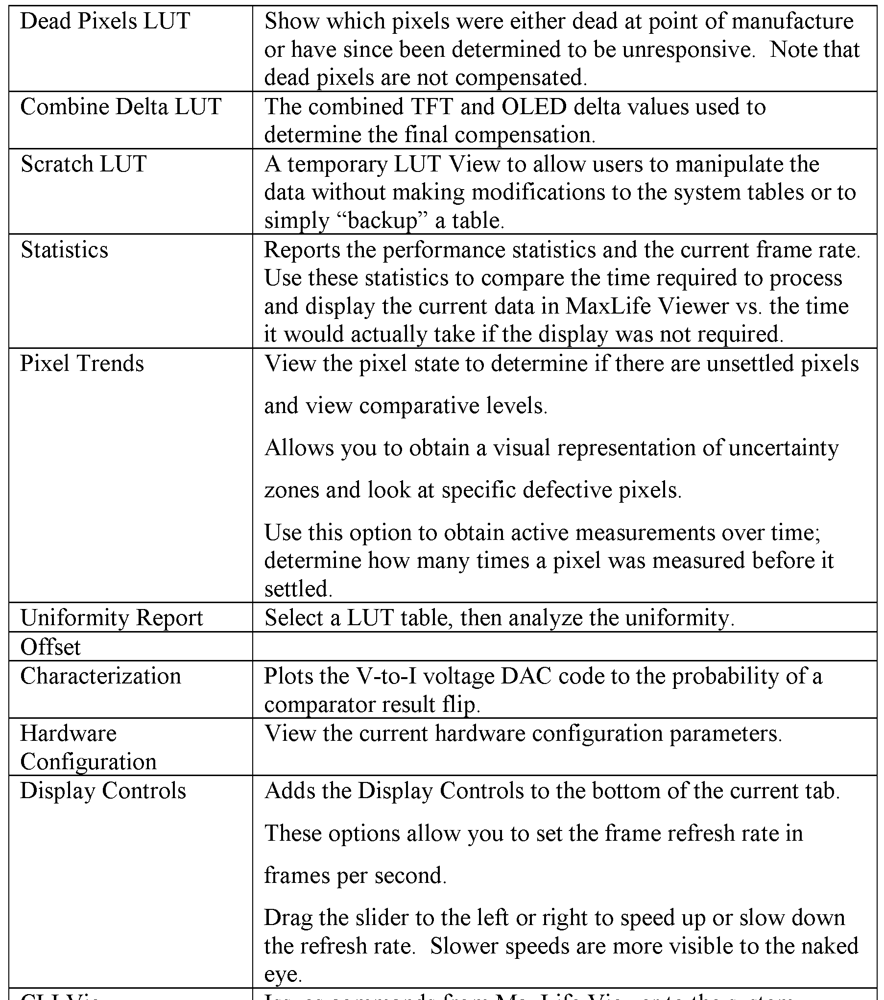
- the circuitry depicted in FIG. 5 takes data from the measurement electronics 13, analyzes that data, and displays it in a wide variety of reports, tables, and pictures. Some of the views are described in the following table:
- TFT Absolute LUT View the absolute measurement replacement values for each pixel on the panel.
- TFT Filtered LUT View the filtered replacement values used to calculate delta values.
- TFT Base LUT View the factory shipment values of the panel to determine how much the pixels have aged (baseline).
- TFT Delta LUT View the difference between the current average measured value and the baseline values (used to determine
- TFT Histogram LUT View the number of times a pixel has been measured since the last time the histogram was reset. This lookup table is primarily used for priority scan algorithm.
- TFT Pixel State LUT View either the current state of the measurement state
- OLED Absolute LUT View the absolute measurement replacement values for each pixel on the panel OLED layer.
- OLED Filtered LUT View the filtered replacement values used to calculate delta values.
- OLED Base LUT View the factory shipment values of the panel to determine how much the pixels have aged (baseline).
- OLED Histogram View the number of times a pixel has been measured since the last time the histogram was reset.
- OLED Pixel State View either the current state of the measurement state
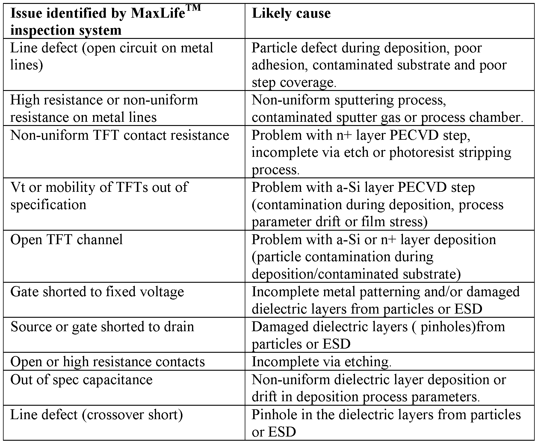
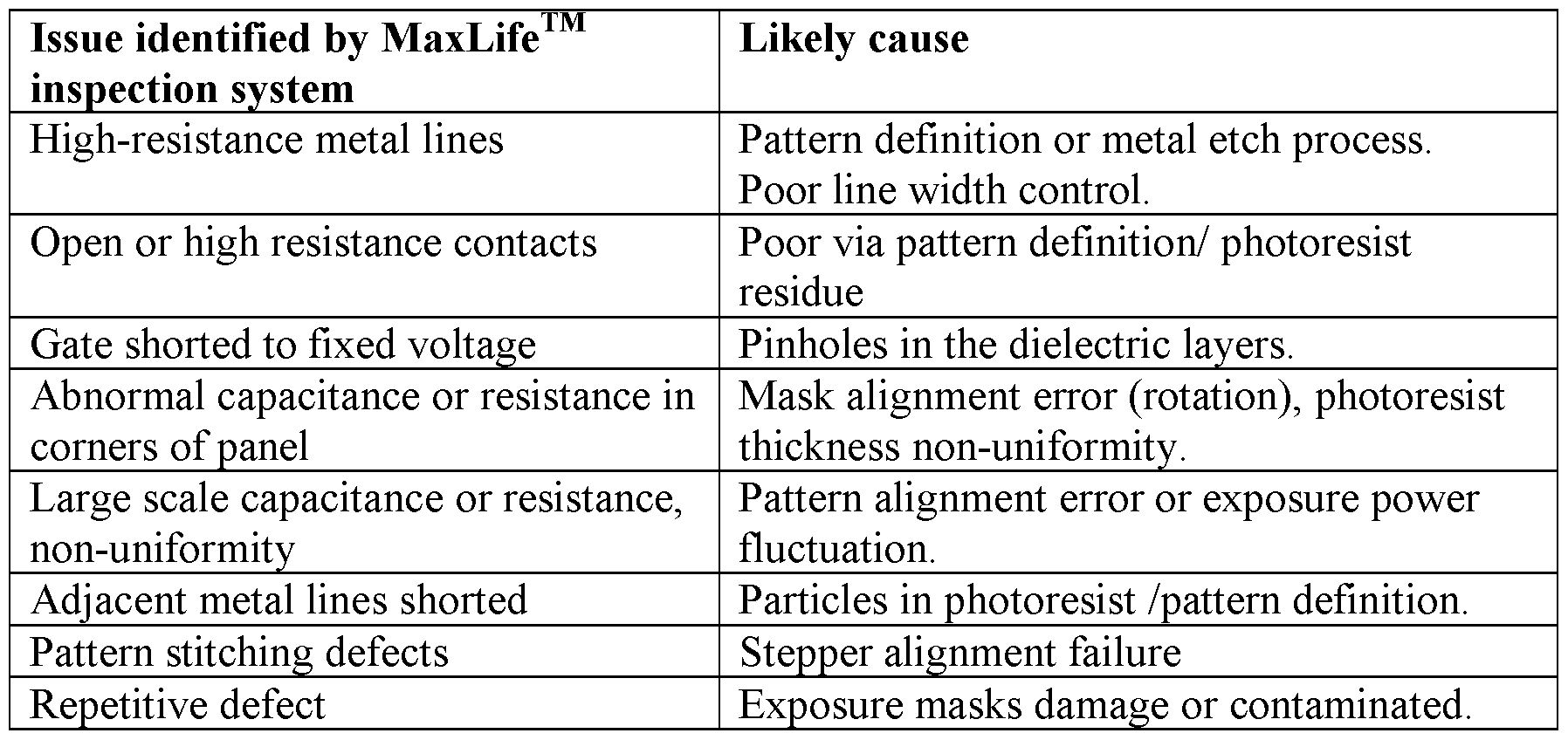
- the inspection system can identify many potential defects and problems (e.g., with sputtering and PECVD steps, that can be used to identify the likely cause of the defect or problem so that the fabricating process can be immediately fine-tuned to correct the problem). Examples of such issues and their likely causes are the following:
- the first measurement can reveal that a problem exists, and specify additional tests that will conclusively identify the exact defect.
- One example is the identification of line defects, which can be detected by any of the following procedures:
- the current can be measured to detect the open defect
- TFTs thin film transistors
- Vt and mobility of each TFT can be used to adjust process annealing parameters, as follows:
- defect location and defect type can be used to pinpoint areas suitable for laser repair (removing material) or ion beam deposition (adding material), as follows:
- Short on metal lines Identify the metal lines that are shorted.
- Open circuit on metal lines Identify the metal lines that are open.
- the uniformity data can also be used to continuously calibrate each print head used for inkjet printing, in real-time. The system knows which print head was used to print each pixel, and thus problems with individual print heads can be detected. The print head used to print those pixels can then be immediately adjusted, as follows.
- the electrical characteristics can be loaded into a lookup table, and used to correct for all TFT and OLED non- uniformities.
- test samples are created around the periphery of the panel, then more details about the global process parameters can be extracted. Typically this is done by cutting off the test samples from a small percentage of displays and putting them in a separate characterization system. However, with the present inspection system, this can be done as part of panel characterization, for every panel, as follows:
- Metal lines can be created and resistance measured. This can test both metal deposition steps and etching.
- Semiconductor layers to be annealed can have their characteristics and uniformity tested.
- OLED structures can be used at different locations around the panel to test alignment.
- OLED structures can be used to test evaporation and inkjet printing steps.
Landscapes
- Engineering & Computer Science (AREA)
- Physics & Mathematics (AREA)
- Computer Hardware Design (AREA)
- General Physics & Mathematics (AREA)
- Theoretical Computer Science (AREA)
- Electroluminescent Light Sources (AREA)
- Manufacturing & Machinery (AREA)
- Devices For Indicating Variable Information By Combining Individual Elements (AREA)
- Microelectronics & Electronic Packaging (AREA)
- Power Engineering (AREA)
Abstract
Description


Claims
Priority Applications (3)
| Application Number | Priority Date | Filing Date | Title |
|---|---|---|---|
| DE112014002086.9T DE112014002086T5 (en) | 2013-04-22 | 2014-04-21 | Test system for OLED display screens |
| CN201910880316.7A CN110634431B (en) | 2013-04-22 | 2014-04-21 | Method for inspecting and manufacturing display panel |
| CN201480022682.4A CN105144361B (en) | 2013-04-22 | 2014-04-21 | Inspection system for OLED display panels |
Applications Claiming Priority (4)
| Application Number | Priority Date | Filing Date | Title |
|---|---|---|---|
| US201361814580P | 2013-04-22 | 2013-04-22 | |
| US61/814,580 | 2013-04-22 | ||
| US201361861614P | 2013-08-02 | 2013-08-02 | |
| US61/861,614 | 2013-08-02 |
Publications (1)
| Publication Number | Publication Date |
|---|---|
| WO2014174427A1 true WO2014174427A1 (en) | 2014-10-30 |
Family
ID=51728347
Family Applications (1)
| Application Number | Title | Priority Date | Filing Date |
|---|---|---|---|
| PCT/IB2014/060879 Ceased WO2014174427A1 (en) | 2013-04-22 | 2014-04-21 | Inspection system for oled display panels |
Country Status (4)
| Country | Link |
|---|---|
| US (1) | US10867536B2 (en) |
| CN (2) | CN105144361B (en) |
| DE (1) | DE112014002086T5 (en) |
| WO (1) | WO2014174427A1 (en) |
Families Citing this family (6)
| Publication number | Priority date | Publication date | Assignee | Title |
|---|---|---|---|---|
| DE202016105307U1 (en) | 2016-09-23 | 2018-01-09 | Reinz-Dichtungs-Gmbh | Flow plate for a humidifier |
| JP6999434B2 (en) * | 2018-01-29 | 2022-01-18 | シャープ株式会社 | Display devices, display systems, and manufacturing methods for display devices. |
| CN109342020B (en) * | 2018-11-20 | 2024-12-03 | 武汉精毅通电子技术有限公司 | A bearing device for display panel testing |
| US11217649B2 (en) * | 2020-04-03 | 2022-01-04 | Star Technologies, Inc. | Method of testing and analyzing display panel |
| CN113409714B (en) * | 2021-06-16 | 2023-01-10 | 合肥鑫晟光电科技有限公司 | Display panel and display device |
| EP4421793A1 (en) * | 2023-02-22 | 2024-08-28 | LX Semicon Co., Ltd. | A driving device and a display device |
Citations (5)
| Publication number | Priority date | Publication date | Assignee | Title |
|---|---|---|---|---|
| US20080158648A1 (en) * | 2006-12-29 | 2008-07-03 | Cummings William J | Peripheral switches for MEMS display test |
| WO2009048618A1 (en) * | 2007-10-11 | 2009-04-16 | Veraconnex, Llc | Probe card test apparatus and method |
| US8208084B2 (en) * | 2008-07-16 | 2012-06-26 | Au Optronics Corporation | Array substrate with test shorting bar and display panel thereof |
| US20120262184A1 (en) * | 2011-04-14 | 2012-10-18 | Au Optronics Corporation | Display panel and testing method thereof |
| US20130309821A1 (en) * | 2009-06-03 | 2013-11-21 | Samsung Display Co., Ltd. | Thin film transistor array substrate for a display panel and a method for manufacturing a thin film transistor array substrate for a display panel |
Family Cites Families (488)
| Publication number | Priority date | Publication date | Assignee | Title |
|---|---|---|---|---|
| US3506851A (en) | 1966-12-14 | 1970-04-14 | North American Rockwell | Field effect transistor driver using capacitor feedback |
| US3774055A (en) | 1972-01-24 | 1973-11-20 | Nat Semiconductor Corp | Clocked bootstrap inverter circuit |
| JPS52119160A (en) | 1976-03-31 | 1977-10-06 | Nec Corp | Semiconductor circuit with insulating gate type field dffect transisto r |
| US4160934A (en) | 1977-08-11 | 1979-07-10 | Bell Telephone Laboratories, Incorporated | Current control circuit for light emitting diode |
| US4354162A (en) | 1981-02-09 | 1982-10-12 | National Semiconductor Corporation | Wide dynamic range control amplifier with offset correction |
| JPS60218626A (en) | 1984-04-13 | 1985-11-01 | Sharp Corp | Color llquid crystal display device |
| JPS61161093A (en) | 1985-01-09 | 1986-07-21 | Sony Corp | Device for correcting dynamic uniformity |
| JPH01272298A (en) | 1988-04-25 | 1989-10-31 | Yamaha Corp | Driving device |
| US4943956A (en) | 1988-04-25 | 1990-07-24 | Yamaha Corporation | Driving apparatus |
| US4996523A (en) | 1988-10-20 | 1991-02-26 | Eastman Kodak Company | Electroluminescent storage display with improved intensity driver circuits |
| US5198803A (en) | 1990-06-06 | 1993-03-30 | Opto Tech Corporation | Large scale movie display system with multiple gray levels |
| JP3039791B2 (en) | 1990-06-08 | 2000-05-08 | 富士通株式会社 | DA converter |
| DE69012110T2 (en) | 1990-06-11 | 1995-03-30 | Ibm | Display device. |
| JPH04132755A (en) | 1990-09-25 | 1992-05-07 | Sumitomo Chem Co Ltd | Vinyl chloride resin composition for powder molding |
| JPH04158570A (en) | 1990-10-22 | 1992-06-01 | Seiko Epson Corp | Structure of semiconductor device and manufacture thereof |
| US5153420A (en) | 1990-11-28 | 1992-10-06 | Xerox Corporation | Timing independent pixel-scale light sensing apparatus |
| US5204661A (en) | 1990-12-13 | 1993-04-20 | Xerox Corporation | Input/output pixel circuit and array of such circuits |
| US5280280A (en) | 1991-05-24 | 1994-01-18 | Robert Hotto | DC integrating display driver employing pixel status memories |
| US5489918A (en) | 1991-06-14 | 1996-02-06 | Rockwell International Corporation | Method and apparatus for dynamically and adjustably generating active matrix liquid crystal display gray level voltages |
| US5589847A (en) | 1991-09-23 | 1996-12-31 | Xerox Corporation | Switched capacitor analog circuits using polysilicon thin film technology |
| US5266515A (en) | 1992-03-02 | 1993-11-30 | Motorola, Inc. | Fabricating dual gate thin film transistors |
| JP2793427B2 (en) * | 1992-04-08 | 1998-09-03 | 株式会社東芝 | Semiconductor device |
| US5572444A (en) | 1992-08-19 | 1996-11-05 | Mtl Systems, Inc. | Method and apparatus for automatic performance evaluation of electronic display devices |
| SG49735A1 (en) | 1993-04-05 | 1998-06-15 | Cirrus Logic Inc | System for compensating crosstalk in LCDS |
| JPH06314977A (en) | 1993-04-28 | 1994-11-08 | Nec Ic Microcomput Syst Ltd | Current output type d/a converter circuit |
| JPH0799321A (en) | 1993-05-27 | 1995-04-11 | Sony Corp | Method and apparatus for manufacturing thin film semiconductor element |
| JPH07120722A (en) | 1993-06-30 | 1995-05-12 | Sharp Corp | Liquid crystal display device and driving method thereof |
| US5557342A (en) | 1993-07-06 | 1996-09-17 | Hitachi, Ltd. | Video display apparatus for displaying a plurality of video signals having different scanning frequencies and a multi-screen display system using the video display apparatus |
| JP3067949B2 (en) | 1994-06-15 | 2000-07-24 | シャープ株式会社 | Electronic device and liquid crystal display device |
| JPH0830231A (en) | 1994-07-18 | 1996-02-02 | Toshiba Corp | LED dot matrix display and dimming method thereof |
| US5714968A (en) | 1994-08-09 | 1998-02-03 | Nec Corporation | Current-dependent light-emitting element drive circuit for use in active matrix display device |
| US6476798B1 (en) | 1994-08-22 | 2002-11-05 | International Game Technology | Reduced noise touch screen apparatus and method |
| US5498880A (en) | 1995-01-12 | 1996-03-12 | E. I. Du Pont De Nemours And Company | Image capture panel using a solid state device |
| US5745660A (en) | 1995-04-26 | 1998-04-28 | Polaroid Corporation | Image rendering system and method for generating stochastic threshold arrays for use therewith |
| US5506499A (en) * | 1995-06-05 | 1996-04-09 | Neomagic Corp. | Multiple probing of an auxilary test pad which allows for reliable bonding to a primary bonding pad |
| US5619033A (en) | 1995-06-07 | 1997-04-08 | Xerox Corporation | Layered solid state photodiode sensor array |
| JPH08340243A (en) | 1995-06-14 | 1996-12-24 | Canon Inc | Bias circuit |
| US5748160A (en) | 1995-08-21 | 1998-05-05 | Mororola, Inc. | Active driven LED matrices |
| JP3272209B2 (en) | 1995-09-07 | 2002-04-08 | アルプス電気株式会社 | LCD drive circuit |
| JPH0990405A (en) | 1995-09-21 | 1997-04-04 | Sharp Corp | Thin film transistor |
| US5945972A (en) | 1995-11-30 | 1999-08-31 | Kabushiki Kaisha Toshiba | Display device |
| JPH09179525A (en) | 1995-12-26 | 1997-07-11 | Pioneer Electron Corp | Method and device for driving capacitive light emitting element |
| US5923794A (en) | 1996-02-06 | 1999-07-13 | Polaroid Corporation | Current-mediated active-pixel image sensing device with current reset |
| US5949398A (en) | 1996-04-12 | 1999-09-07 | Thomson Multimedia S.A. | Select line driver for a display matrix with toggling backplane |
| US6271825B1 (en) | 1996-04-23 | 2001-08-07 | Rainbow Displays, Inc. | Correction methods for brightness in electronic display |
| US5723950A (en) | 1996-06-10 | 1998-03-03 | Motorola | Pre-charge driver for light emitting devices and method |
| JP3266177B2 (en) | 1996-09-04 | 2002-03-18 | 住友電気工業株式会社 | Current mirror circuit, reference voltage generating circuit and light emitting element driving circuit using the same |
| US5952991A (en) | 1996-11-14 | 1999-09-14 | Kabushiki Kaisha Toshiba | Liquid crystal display |
| US6261009B1 (en) | 1996-11-27 | 2001-07-17 | Zih Corporation | Thermal printer |
| US5874803A (en) | 1997-09-09 | 1999-02-23 | The Trustees Of Princeton University | Light emitting device with stack of OLEDS and phosphor downconverter |
| TW441136B (en) | 1997-01-28 | 2001-06-16 | Casio Computer Co Ltd | An electroluminescent display device and a driving method thereof |
| US5917280A (en) | 1997-02-03 | 1999-06-29 | The Trustees Of Princeton University | Stacked organic light emitting devices |
| KR100509241B1 (en) | 1997-02-17 | 2005-08-23 | 세이코 엡슨 가부시키가이샤 | Display device |
| WO1998040871A1 (en) | 1997-03-12 | 1998-09-17 | Seiko Epson Corporation | Pixel circuit, display device and electronic equipment having current-driven light-emitting device |
| JPH10254410A (en) | 1997-03-12 | 1998-09-25 | Pioneer Electron Corp | Organic electroluminescent display device, and driving method therefor |
| US5903248A (en) | 1997-04-11 | 1999-05-11 | Spatialight, Inc. | Active matrix display having pixel driving circuits with integrated charge pumps |
| US5952789A (en) | 1997-04-14 | 1999-09-14 | Sarnoff Corporation | Active matrix organic light emitting diode (amoled) display pixel structure and data load/illuminate circuit therefor |
| US6229506B1 (en) | 1997-04-23 | 2001-05-08 | Sarnoff Corporation | Active matrix light emitting diode pixel structure and concomitant method |
| JP4251377B2 (en) | 1997-04-23 | 2009-04-08 | 宇東科技股▲ふん▼有限公司 | Active matrix light emitting diode pixel structure and method |
| US5815303A (en) | 1997-06-26 | 1998-09-29 | Xerox Corporation | Fault tolerant projective display having redundant light modulators |
| US6023259A (en) | 1997-07-11 | 2000-02-08 | Fed Corporation | OLED active matrix using a single transistor current mode pixel design |
| KR100323441B1 (en) | 1997-08-20 | 2002-06-20 | 윤종용 | Mpeg2 motion picture coding/decoding system |
| US20010043173A1 (en) | 1997-09-04 | 2001-11-22 | Ronald Roy Troutman | Field sequential gray in active matrix led display using complementary transistor pixel circuits |
| JPH1187720A (en) | 1997-09-08 | 1999-03-30 | Sanyo Electric Co Ltd | Semiconductor device and liquid crystal display device |
| JPH1196333A (en) | 1997-09-16 | 1999-04-09 | Olympus Optical Co Ltd | Color image processing equipment |
| US6738035B1 (en) | 1997-09-22 | 2004-05-18 | Nongqiang Fan | Active matrix LCD based on diode switches and methods of improving display uniformity of same |
| JP3767877B2 (en) | 1997-09-29 | 2006-04-19 | 三菱化学株式会社 | Active matrix light emitting diode pixel structure and method thereof |
| US6909419B2 (en) | 1997-10-31 | 2005-06-21 | Kopin Corporation | Portable microdisplay system |
| US6069365A (en) | 1997-11-25 | 2000-05-30 | Alan Y. Chow | Optical processor based imaging system |
| JP3755277B2 (en) | 1998-01-09 | 2006-03-15 | セイコーエプソン株式会社 | Electro-optical device drive circuit, electro-optical device, and electronic apparatus |
| JPH11231805A (en) | 1998-02-10 | 1999-08-27 | Sanyo Electric Co Ltd | Display device |
| US6445369B1 (en) | 1998-02-20 | 2002-09-03 | The University Of Hong Kong | Light emitting diode dot matrix display system with audio output |
| US6259424B1 (en) | 1998-03-04 | 2001-07-10 | Victor Company Of Japan, Ltd. | Display matrix substrate, production method of the same and display matrix circuit |
| FR2775821B1 (en) | 1998-03-05 | 2000-05-26 | Jean Claude Decaux | LIGHT DISPLAY PANEL |
| US6097360A (en) | 1998-03-19 | 2000-08-01 | Holloman; Charles J | Analog driver for LED or similar display element |
| JP3252897B2 (en) | 1998-03-31 | 2002-02-04 | 日本電気株式会社 | Element driving device and method, image display device |
| JP2931975B1 (en) | 1998-05-25 | 1999-08-09 | アジアエレクトロニクス株式会社 | TFT array inspection method and device |
| JP3702096B2 (en) | 1998-06-08 | 2005-10-05 | 三洋電機株式会社 | Thin film transistor and display device |
| GB9812742D0 (en) | 1998-06-12 | 1998-08-12 | Philips Electronics Nv | Active matrix electroluminescent display devices |
| JP2000075854A (en) | 1998-06-18 | 2000-03-14 | Matsushita Electric Ind Co Ltd | Image processing device and display device using the same |
| CA2242720C (en) | 1998-07-09 | 2000-05-16 | Ibm Canada Limited-Ibm Canada Limitee | Programmable led driver |
| JP2953465B1 (en) | 1998-08-14 | 1999-09-27 | 日本電気株式会社 | Constant current drive circuit |
| EP0984492A3 (en) | 1998-08-31 | 2000-05-17 | Sel Semiconductor Energy Laboratory Co., Ltd. | Semiconductor device comprising organic resin and process for producing semiconductor device |
| JP2000081607A (en) | 1998-09-04 | 2000-03-21 | Denso Corp | Matrix type liquid crystal display device |
| US6940300B1 (en) * | 1998-09-23 | 2005-09-06 | International Business Machines Corporation | Integrated circuits for testing an active matrix display array |
| US6417825B1 (en) | 1998-09-29 | 2002-07-09 | Sarnoff Corporation | Analog active matrix emissive display |
| US6501098B2 (en) | 1998-11-25 | 2002-12-31 | Semiconductor Energy Laboratory Co, Ltd. | Semiconductor device |
| JP3423232B2 (en) | 1998-11-30 | 2003-07-07 | 三洋電機株式会社 | Active EL display |
| JP3031367B1 (en) | 1998-12-02 | 2000-04-10 | 日本電気株式会社 | Image sensor |
| JP2000174282A (en) | 1998-12-03 | 2000-06-23 | Semiconductor Energy Lab Co Ltd | Semiconductor device |
| AU2361600A (en) | 1998-12-14 | 2000-07-03 | Kopin Corporation | Portable microdisplay system |
| US6639244B1 (en) | 1999-01-11 | 2003-10-28 | Semiconductor Energy Laboratory Co., Ltd. | Semiconductor device and method of fabricating the same |
| JP3686769B2 (en) | 1999-01-29 | 2005-08-24 | 日本電気株式会社 | Organic EL element driving apparatus and driving method |
| JP2000231346A (en) | 1999-02-09 | 2000-08-22 | Sanyo Electric Co Ltd | Electroluminescence display device |
| US7122835B1 (en) | 1999-04-07 | 2006-10-17 | Semiconductor Energy Laboratory Co., Ltd. | Electrooptical device and a method of manufacturing the same |
| US7012600B2 (en) | 1999-04-30 | 2006-03-14 | E Ink Corporation | Methods for driving bistable electro-optic displays, and apparatus for use therein |
| JP4565700B2 (en) | 1999-05-12 | 2010-10-20 | ルネサスエレクトロニクス株式会社 | Semiconductor device |
| US6690344B1 (en) | 1999-05-14 | 2004-02-10 | Ngk Insulators, Ltd. | Method and apparatus for driving device and display |
| KR100296113B1 (en) | 1999-06-03 | 2001-07-12 | 구본준, 론 위라하디락사 | ElectroLuminescent Display |
| JP4092857B2 (en) | 1999-06-17 | 2008-05-28 | ソニー株式会社 | Image display device |
| US6437106B1 (en) | 1999-06-24 | 2002-08-20 | Abbott Laboratories | Process for preparing 6-o-substituted erythromycin derivatives |
| US7379039B2 (en) | 1999-07-14 | 2008-05-27 | Sony Corporation | Current drive circuit and display device using same pixel circuit, and drive method |
| EP1130565A4 (en) | 1999-07-14 | 2006-10-04 | Sony Corp | ATTACK CIRCUIT AND DISPLAY INCLUDING THE SAME, PIXEL CIRCUIT, AND ATTACK METHOD |
| EP1129446A1 (en) | 1999-09-11 | 2001-09-05 | Koninklijke Philips Electronics N.V. | Active matrix electroluminescent display device |
| GB9923261D0 (en) | 1999-10-02 | 1999-12-08 | Koninkl Philips Electronics Nv | Active matrix electroluminescent display device |
| KR20020025984A (en) | 1999-10-04 | 2002-04-04 | 모리시타 요이찌 | Method of driving display panel, and display panel luminance correction device and display panel driving device |
| WO2001027910A1 (en) | 1999-10-12 | 2001-04-19 | Koninklijke Philips Electronics N.V. | Led display device |
| US6392617B1 (en) | 1999-10-27 | 2002-05-21 | Agilent Technologies, Inc. | Active matrix light emitting diode display |
| JP2001134217A (en) | 1999-11-09 | 2001-05-18 | Tdk Corp | Driving device for organic el element |
| JP2001147659A (en) | 1999-11-18 | 2001-05-29 | Sony Corp | Display device |
| TW587239B (en) | 1999-11-30 | 2004-05-11 | Semiconductor Energy Lab | Electric device |
| GB9929501D0 (en) | 1999-12-14 | 2000-02-09 | Koninkl Philips Electronics Nv | Image sensor |
| TW573165B (en) | 1999-12-24 | 2004-01-21 | Sanyo Electric Co | Display device |
| US6307322B1 (en) | 1999-12-28 | 2001-10-23 | Sarnoff Corporation | Thin-film transistor circuitry with reduced sensitivity to variance in transistor threshold voltage |
| JP2001195014A (en) | 2000-01-14 | 2001-07-19 | Tdk Corp | Driving device for organic el element |
| JP4907753B2 (en) | 2000-01-17 | 2012-04-04 | エーユー オプトロニクス コーポレイション | Liquid crystal display |
| US6809710B2 (en) | 2000-01-21 | 2004-10-26 | Emagin Corporation | Gray scale pixel driver for electronic display and method of operation therefor |
| US6639265B2 (en) | 2000-01-26 | 2003-10-28 | Semiconductor Energy Laboratory Co., Ltd. | Semiconductor device and method of manufacturing the semiconductor device |
| US7030921B2 (en) | 2000-02-01 | 2006-04-18 | Minolta Co., Ltd. | Solid-state image-sensing device |
| US6414661B1 (en) | 2000-02-22 | 2002-07-02 | Sarnoff Corporation | Method and apparatus for calibrating display devices and automatically compensating for loss in their efficiency over time |
| TW521226B (en) | 2000-03-27 | 2003-02-21 | Semiconductor Energy Lab | Electro-optical device |
| JP2001284592A (en) | 2000-03-29 | 2001-10-12 | Sony Corp | Thin film semiconductor device and driving method thereof |
| US6528950B2 (en) | 2000-04-06 | 2003-03-04 | Semiconductor Energy Laboratory Co., Ltd. | Electronic device and driving method |
| US6611108B2 (en) | 2000-04-26 | 2003-08-26 | Semiconductor Energy Laboratory Co., Ltd. | Electronic device and driving method thereof |
| US6583576B2 (en) | 2000-05-08 | 2003-06-24 | Semiconductor Energy Laboratory Co., Ltd. | Light-emitting device, and electric device using the same |
| TW493153B (en) | 2000-05-22 | 2002-07-01 | Koninkl Philips Electronics Nv | Display device |
| EP1158483A3 (en) | 2000-05-24 | 2003-02-05 | Eastman Kodak Company | Solid-state display with reference pixel |
| JP4703815B2 (en) | 2000-05-26 | 2011-06-15 | 株式会社半導体エネルギー研究所 | MOS type sensor driving method and imaging method |
| TW461002B (en) | 2000-06-05 | 2001-10-21 | Ind Tech Res Inst | Testing apparatus and testing method for organic light emitting diode array |
| JP4831889B2 (en) | 2000-06-22 | 2011-12-07 | 株式会社半導体エネルギー研究所 | Display device |
| JP3877049B2 (en) | 2000-06-27 | 2007-02-07 | 株式会社日立製作所 | Image display apparatus and driving method thereof |
| US6738034B2 (en) | 2000-06-27 | 2004-05-18 | Hitachi, Ltd. | Picture image display device and method of driving the same |
| JP2002032058A (en) | 2000-07-18 | 2002-01-31 | Nec Corp | Display device |
| JP3437152B2 (en) | 2000-07-28 | 2003-08-18 | ウインテスト株式会社 | Apparatus and method for evaluating organic EL display |
| JP2002049325A (en) | 2000-07-31 | 2002-02-15 | Seiko Instruments Inc | Illuminator for correcting display color temperature and flat panel display |
| US6304039B1 (en) | 2000-08-08 | 2001-10-16 | E-Lite Technologies, Inc. | Power supply for illuminating an electro-luminescent panel |
| JP3485175B2 (en) | 2000-08-10 | 2004-01-13 | 日本電気株式会社 | Electroluminescent display |
| US6828950B2 (en) | 2000-08-10 | 2004-12-07 | Semiconductor Energy Laboratory Co., Ltd. | Display device and method of driving the same |
| TW507192B (en) | 2000-09-18 | 2002-10-21 | Sanyo Electric Co | Display device |
| JP2002162934A (en) | 2000-09-29 | 2002-06-07 | Eastman Kodak Co | Flat-panel display with luminance feedback |
| JP3838063B2 (en) | 2000-09-29 | 2006-10-25 | セイコーエプソン株式会社 | Driving method of organic electroluminescence device |
| JP4925528B2 (en) | 2000-09-29 | 2012-04-25 | 三洋電機株式会社 | Display device |
| US6781567B2 (en) | 2000-09-29 | 2004-08-24 | Seiko Epson Corporation | Driving method for electro-optical device, electro-optical device, and electronic apparatus |
| US7315295B2 (en) | 2000-09-29 | 2008-01-01 | Seiko Epson Corporation | Driving method for electro-optical device, electro-optical device, and electronic apparatus |
| TW550530B (en) | 2000-10-27 | 2003-09-01 | Semiconductor Energy Lab | Display device and method of driving the same |
| JP2002141420A (en) | 2000-10-31 | 2002-05-17 | Mitsubishi Electric Corp | Semiconductor device and manufacturing method thereof |
| US6320325B1 (en) | 2000-11-06 | 2001-11-20 | Eastman Kodak Company | Emissive display with luminance feedback from a representative pixel |
| US7127380B1 (en) | 2000-11-07 | 2006-10-24 | Alliant Techsystems Inc. | System for performing coupled finite analysis |
| KR100405026B1 (en) | 2000-12-22 | 2003-11-07 | 엘지.필립스 엘시디 주식회사 | Liquid Crystal Display |
| TW561445B (en) | 2001-01-02 | 2003-11-11 | Chi Mei Optoelectronics Corp | OLED active driving system with current feedback |
| US6580657B2 (en) | 2001-01-04 | 2003-06-17 | International Business Machines Corporation | Low-power organic light emitting diode pixel circuit |
| JP3593982B2 (en) | 2001-01-15 | 2004-11-24 | ソニー株式会社 | Active matrix type display device, active matrix type organic electroluminescence display device, and driving method thereof |
| US6323631B1 (en) | 2001-01-18 | 2001-11-27 | Sunplus Technology Co., Ltd. | Constant current driver with auto-clamped pre-charge function |
| JP2002215063A (en) | 2001-01-19 | 2002-07-31 | Sony Corp | Active matrix display |
| TW569016B (en) | 2001-01-29 | 2004-01-01 | Semiconductor Energy Lab | Light emitting device |
| CN1302313C (en) | 2001-02-05 | 2007-02-28 | 国际商业机器公司 | Liquid crystal display device |
| TWI248319B (en) | 2001-02-08 | 2006-01-21 | Semiconductor Energy Lab | Light emitting device and electronic equipment using the same |
| JP2002244617A (en) | 2001-02-15 | 2002-08-30 | Sanyo Electric Co Ltd | Organic el pixel circuit |
| JP4392165B2 (en) | 2001-02-16 | 2009-12-24 | イグニス・イノベイション・インコーポレーテッド | Organic light emitting diode display with shielding electrode |
| US7569849B2 (en) | 2001-02-16 | 2009-08-04 | Ignis Innovation Inc. | Pixel driver circuit and pixel circuit having the pixel driver circuit |
| CA2438577C (en) | 2001-02-16 | 2006-08-22 | Ignis Innovation Inc. | Pixel current driver for organic light emitting diode displays |
| WO2002067327A2 (en) | 2001-02-16 | 2002-08-29 | Ignis Innovation Inc. | Pixel current driver for organic light emitting diode displays |
| US7061451B2 (en) | 2001-02-21 | 2006-06-13 | Semiconductor Energy Laboratory Co., Ltd, | Light emitting device and electronic device |
| JP4212815B2 (en) | 2001-02-21 | 2009-01-21 | 株式会社半導体エネルギー研究所 | Light emitting device |
| US6753654B2 (en) | 2001-02-21 | 2004-06-22 | Semiconductor Energy Laboratory Co., Ltd. | Light emitting device and electronic appliance |
| US7352786B2 (en) | 2001-03-05 | 2008-04-01 | Fuji Xerox Co., Ltd. | Apparatus for driving light emitting element and system for driving light emitting element |
| JP2002278513A (en) | 2001-03-19 | 2002-09-27 | Sharp Corp | Electro-optical device |
| JPWO2002075709A1 (en) | 2001-03-21 | 2004-07-08 | キヤノン株式会社 | Driver circuit for active matrix light emitting device |
| US7164417B2 (en) | 2001-03-26 | 2007-01-16 | Eastman Kodak Company | Dynamic controller for active-matrix displays |
| JP3819723B2 (en) | 2001-03-30 | 2006-09-13 | 株式会社日立製作所 | Display device and driving method thereof |
| JP4785271B2 (en) | 2001-04-27 | 2011-10-05 | 株式会社半導体エネルギー研究所 | Liquid crystal display device, electronic equipment |
| US7136058B2 (en) | 2001-04-27 | 2006-11-14 | Kabushiki Kaisha Toshiba | Display apparatus, digital-to-analog conversion circuit and digital-to-analog conversion method |
| US6943761B2 (en) | 2001-05-09 | 2005-09-13 | Clare Micronix Integrated Systems, Inc. | System for providing pulse amplitude modulation for OLED display drivers |
| US6594606B2 (en) | 2001-05-09 | 2003-07-15 | Clare Micronix Integrated Systems, Inc. | Matrix element voltage sensing for precharge |
| JP2002351409A (en) | 2001-05-23 | 2002-12-06 | Internatl Business Mach Corp <Ibm> | Liquid crystal display device, liquid crystal display driving circuit, driving method for liquid crystal display, and program |
| US6777249B2 (en) | 2001-06-01 | 2004-08-17 | Semiconductor Energy Laboratory Co., Ltd. | Method of repairing a light-emitting device, and method of manufacturing a light-emitting device |
| US7012588B2 (en) | 2001-06-05 | 2006-03-14 | Eastman Kodak Company | Method for saving power in an organic electroluminescent display using white light emitting elements |
| KR100743103B1 (en) | 2001-06-22 | 2007-07-27 | 엘지.필립스 엘시디 주식회사 | Electro luminescence panel |
| KR100593276B1 (en) | 2001-06-22 | 2006-06-26 | 탑폴리 옵토일렉트로닉스 코포레이션 | Organic light emitting diode pixel circuit driving method and driver |
| US6956547B2 (en) | 2001-06-30 | 2005-10-18 | Lg.Philips Lcd Co., Ltd. | Driving circuit and method of driving an organic electroluminescence device |
| JP2003043994A (en) | 2001-07-27 | 2003-02-14 | Canon Inc | Active matrix display |
| JP3800050B2 (en) | 2001-08-09 | 2006-07-19 | 日本電気株式会社 | Display device drive circuit |
| CN101257743B (en) | 2001-08-29 | 2011-05-25 | 株式会社半导体能源研究所 | Light emitting device and driving method of the light emitting device |
| US7027015B2 (en) | 2001-08-31 | 2006-04-11 | Intel Corporation | Compensating organic light emitting device displays for color variations |
| JP2003076331A (en) | 2001-08-31 | 2003-03-14 | Seiko Epson Corp | Display device and electronic equipment |
| KR100714513B1 (en) | 2001-09-07 | 2007-05-07 | 마츠시타 덴끼 산교 가부시키가이샤 | Drive circuit of EL display device, electronic display device and EL display device |
| US7088052B2 (en) | 2001-09-07 | 2006-08-08 | Semiconductor Energy Laboratory Co., Ltd. | Light emitting device and method of driving the same |
| US6525683B1 (en) | 2001-09-19 | 2003-02-25 | Intel Corporation | Nonlinearly converting a signal to compensate for non-uniformities and degradations in a display |
| KR100924739B1 (en) | 2001-09-21 | 2009-11-05 | 가부시키가이샤 한도오따이 에네루기 켄큐쇼 | Display device and driving method |
| CN1559064A (en) | 2001-09-25 | 2004-12-29 | ���µ�����ҵ��ʽ���� | EL display panel and EL display device using the same |
| JP3725458B2 (en) | 2001-09-25 | 2005-12-14 | シャープ株式会社 | Active matrix display panel and image display device having the same |
| SG120889A1 (en) | 2001-09-28 | 2006-04-26 | Semiconductor Energy Lab | A light emitting device and electronic apparatus using the same |
| JP4067803B2 (en) | 2001-10-11 | 2008-03-26 | シャープ株式会社 | Light emitting diode driving circuit and optical transmission device using the same |
| US20030071821A1 (en) | 2001-10-11 | 2003-04-17 | Sundahl Robert C. | Luminance compensation for emissive displays |
| AU2002335856A1 (en) | 2001-10-19 | 2003-04-28 | Clare Micronix Integrated Systems, Inc. | Method and system for charge pump active gate drive |
| WO2003034389A2 (en) | 2001-10-19 | 2003-04-24 | Clare Micronix Integrated Systems, Inc. | System and method for providing pulse amplitude modulation for oled display drivers |
| US6861810B2 (en) | 2001-10-23 | 2005-03-01 | Fpd Systems | Organic electroluminescent display device driving method and apparatus |
| KR100433216B1 (en) | 2001-11-06 | 2004-05-27 | 엘지.필립스 엘시디 주식회사 | Apparatus and method of driving electro luminescence panel |
| KR100940342B1 (en) | 2001-11-13 | 2010-02-04 | 가부시키가이샤 한도오따이 에네루기 켄큐쇼 | Display device and driving method |
| US7061263B1 (en) * | 2001-11-15 | 2006-06-13 | Inapac Technology, Inc. | Layout and use of bond pads and probe pads for testing of integrated circuits devices |
| US7071932B2 (en) | 2001-11-20 | 2006-07-04 | Toppoly Optoelectronics Corporation | Data voltage current drive amoled pixel circuit |
| US20040070565A1 (en) | 2001-12-05 | 2004-04-15 | Nayar Shree K | Method and apparatus for displaying images |
| JP4009097B2 (en) | 2001-12-07 | 2007-11-14 | 日立電線株式会社 | LIGHT EMITTING DEVICE, ITS MANUFACTURING METHOD, AND LEAD FRAME USED FOR MANUFACTURING LIGHT EMITTING DEVICE |
| JP2003177709A (en) | 2001-12-13 | 2003-06-27 | Seiko Epson Corp | Pixel circuit for light emitting element |
| JP3800404B2 (en) | 2001-12-19 | 2006-07-26 | 株式会社日立製作所 | Image display device |
| GB0130411D0 (en) | 2001-12-20 | 2002-02-06 | Koninkl Philips Electronics Nv | Active matrix electroluminescent display device |
| CN1293421C (en) | 2001-12-27 | 2007-01-03 | Lg.菲利浦Lcd株式会社 | Electroluminescent display panel and method for operating it |
| US7274363B2 (en) | 2001-12-28 | 2007-09-25 | Pioneer Corporation | Panel display driving device and driving method |
| JP2003255901A (en) | 2001-12-28 | 2003-09-10 | Sanyo Electric Co Ltd | Organic el display luminance control method and luminance control circuit |
| JP4029840B2 (en) | 2002-01-17 | 2008-01-09 | 日本電気株式会社 | Semiconductor device having matrix type current load driving circuit and driving method thereof |
| JP2003295825A (en) | 2002-02-04 | 2003-10-15 | Sanyo Electric Co Ltd | Display device |
| US6947022B2 (en) | 2002-02-11 | 2005-09-20 | National Semiconductor Corporation | Display line drivers and method for signal propagation delay compensation |
| US6720942B2 (en) | 2002-02-12 | 2004-04-13 | Eastman Kodak Company | Flat-panel light emitting pixel with luminance feedback |
| JP2003308046A (en) | 2002-02-18 | 2003-10-31 | Sanyo Electric Co Ltd | Display device |
| JP3613253B2 (en) | 2002-03-14 | 2005-01-26 | 日本電気株式会社 | Current control element drive circuit and image display device |
| US7876294B2 (en) | 2002-03-05 | 2011-01-25 | Nec Corporation | Image display and its control method |
| WO2003077231A2 (en) | 2002-03-13 | 2003-09-18 | Koninklijke Philips Electronics N.V. | Two sided display device |
| GB2386462A (en) | 2002-03-14 | 2003-09-17 | Cambridge Display Tech Ltd | Display driver circuits |
| JP4274734B2 (en) | 2002-03-15 | 2009-06-10 | 三洋電機株式会社 | Transistor circuit |
| JP3995505B2 (en) | 2002-03-25 | 2007-10-24 | 三洋電機株式会社 | Display method and display device |
| JP4266682B2 (en) | 2002-03-29 | 2009-05-20 | セイコーエプソン株式会社 | Electronic device, driving method of electronic device, electro-optical device, and electronic apparatus |
| US6806497B2 (en) | 2002-03-29 | 2004-10-19 | Seiko Epson Corporation | Electronic device, method for driving the electronic device, electro-optical device, and electronic equipment |
| KR100488835B1 (en) | 2002-04-04 | 2005-05-11 | 산요덴키가부시키가이샤 | Semiconductor device and display device |
| US20050174045A1 (en) * | 2002-04-04 | 2005-08-11 | Dielectric Systems, Inc. | Organic light-emitting device display having a plurality of passive polymer layers |
| US6911781B2 (en) | 2002-04-23 | 2005-06-28 | Semiconductor Energy Laboratory Co., Ltd. | Light emitting device and production system of the same |
| JP3637911B2 (en) | 2002-04-24 | 2005-04-13 | セイコーエプソン株式会社 | Electronic device, electronic apparatus, and driving method of electronic device |
| JP2003317944A (en) | 2002-04-26 | 2003-11-07 | Seiko Epson Corp | Electro-optical devices and electronic equipment |
| US7474285B2 (en) | 2002-05-17 | 2009-01-06 | Semiconductor Energy Laboratory Co., Ltd. | Display apparatus and driving method thereof |
| US6909243B2 (en) | 2002-05-17 | 2005-06-21 | Semiconductor Energy Laboratory Co., Ltd. | Light-emitting device and method of driving the same |
| JP3527726B2 (en) | 2002-05-21 | 2004-05-17 | ウインテスト株式会社 | Inspection method and inspection device for active matrix substrate |
| JP3972359B2 (en) | 2002-06-07 | 2007-09-05 | カシオ計算機株式会社 | Display device |
| JP2004070293A (en) | 2002-06-12 | 2004-03-04 | Seiko Epson Corp | Electronic device, method of driving electronic device, and electronic apparatus |
| TW582006B (en) | 2002-06-14 | 2004-04-01 | Chunghwa Picture Tubes Ltd | Brightness correction apparatus and method for plasma display |
| GB2389952A (en) | 2002-06-18 | 2003-12-24 | Cambridge Display Tech Ltd | Driver circuits for electroluminescent displays with reduced power consumption |
| GB2389951A (en) | 2002-06-18 | 2003-12-24 | Cambridge Display Tech Ltd | Display driver circuits for active matrix OLED displays |
| US20030230980A1 (en) | 2002-06-18 | 2003-12-18 | Forrest Stephen R | Very low voltage, high efficiency phosphorescent oled in a p-i-n structure |
| US6668645B1 (en) | 2002-06-18 | 2003-12-30 | Ti Group Automotive Systems, L.L.C. | Optical fuel level sensor |
| JP3970110B2 (en) | 2002-06-27 | 2007-09-05 | カシオ計算機株式会社 | CURRENT DRIVE DEVICE, ITS DRIVE METHOD, AND DISPLAY DEVICE USING CURRENT DRIVE DEVICE |
| JP2004045488A (en) | 2002-07-09 | 2004-02-12 | Casio Comput Co Ltd | Display drive device and drive control method thereof |
| JP4115763B2 (en) | 2002-07-10 | 2008-07-09 | パイオニア株式会社 | Display device and display method |
| TW594628B (en) | 2002-07-12 | 2004-06-21 | Au Optronics Corp | Cell pixel driving circuit of OLED |
| US20040150594A1 (en) | 2002-07-25 | 2004-08-05 | Semiconductor Energy Laboratory Co., Ltd. | Display device and drive method therefor |
| JP3829778B2 (en) | 2002-08-07 | 2006-10-04 | セイコーエプソン株式会社 | Electronic circuit, electro-optical device, and electronic apparatus |
| GB0219771D0 (en) | 2002-08-24 | 2002-10-02 | Koninkl Philips Electronics Nv | Manufacture of electronic devices comprising thin-film circuit elements |
| TW558699B (en) | 2002-08-28 | 2003-10-21 | Au Optronics Corp | Driving circuit and method for light emitting device |
| JP4194451B2 (en) | 2002-09-02 | 2008-12-10 | キヤノン株式会社 | Drive circuit, display device, and information display device |
| US7385572B2 (en) | 2002-09-09 | 2008-06-10 | E.I Du Pont De Nemours And Company | Organic electronic device having improved homogeneity |
| JP2005539252A (en) | 2002-09-16 | 2005-12-22 | コーニンクレッカ フィリップス エレクトロニクス エヌ ヴィ | Display device |
| TW564390B (en) | 2002-09-16 | 2003-12-01 | Au Optronics Corp | Driving circuit and method for light emitting device |
| TW588468B (en) | 2002-09-19 | 2004-05-21 | Ind Tech Res Inst | Pixel structure of active matrix organic light-emitting diode |
| JP4230746B2 (en) | 2002-09-30 | 2009-02-25 | パイオニア株式会社 | Display device and display panel driving method |
| GB0223304D0 (en) | 2002-10-08 | 2002-11-13 | Koninkl Philips Electronics Nv | Electroluminescent display devices |
| JP3832415B2 (en) | 2002-10-11 | 2006-10-11 | ソニー株式会社 | Active matrix display device |
| JP4032922B2 (en) | 2002-10-28 | 2008-01-16 | 三菱電機株式会社 | Display device and display panel |
| DE10250827B3 (en) | 2002-10-31 | 2004-07-15 | OCé PRINTING SYSTEMS GMBH | Imaging optimization control device for electrographic process providing temperature compensation for photosensitive layer and exposure light source |
| KR100476368B1 (en) | 2002-11-05 | 2005-03-17 | 엘지.필립스 엘시디 주식회사 | Data driving apparatus and method of organic electro-luminescence display panel |
| CN1711479B (en) | 2002-11-06 | 2010-05-26 | 统宝光电股份有限公司 | Method and device for inspecting LED matrix display |
| US6911964B2 (en) | 2002-11-07 | 2005-06-28 | Duke University | Frame buffer pixel circuit for liquid crystal display |
| JP2004157467A (en) | 2002-11-08 | 2004-06-03 | Tohoku Pioneer Corp | Driving method and driving-gear of active type light emitting display panel |
| US6687266B1 (en) | 2002-11-08 | 2004-02-03 | Universal Display Corporation | Organic light emitting materials and devices |
| US20040095297A1 (en) | 2002-11-20 | 2004-05-20 | International Business Machines Corporation | Nonlinear voltage controlled current source with feedback circuit |
| JP2006507524A (en) | 2002-11-21 | 2006-03-02 | コーニンクレッカ フィリップス エレクトロニクス エヌ ヴィ | Method for improving display output uniformity |
| JP3707484B2 (en) | 2002-11-27 | 2005-10-19 | セイコーエプソン株式会社 | Electro-optical device, driving method of electro-optical device, and electronic apparatus |
| JP2004191627A (en) | 2002-12-11 | 2004-07-08 | Hitachi Ltd | Organic light emitting display |
| JP2004191752A (en) | 2002-12-12 | 2004-07-08 | Seiko Epson Corp | Electro-optical device, electro-optical device driving method, and electronic apparatus |
| US7075242B2 (en) | 2002-12-16 | 2006-07-11 | Eastman Kodak Company | Color OLED display system having improved performance |
| TWI228941B (en) | 2002-12-27 | 2005-03-01 | Au Optronics Corp | Active matrix organic light emitting diode display and fabricating method thereof |
| JP4865986B2 (en) | 2003-01-10 | 2012-02-01 | グローバル・オーエルイーディー・テクノロジー・リミテッド・ライアビリティ・カンパニー | Organic EL display device |
| US7079091B2 (en) | 2003-01-14 | 2006-07-18 | Eastman Kodak Company | Compensating for aging in OLED devices |
| US7184054B2 (en) | 2003-01-21 | 2007-02-27 | Hewlett-Packard Development Company, L.P. | Correction of a projected image based on a reflected image |
| KR100490622B1 (en) | 2003-01-21 | 2005-05-17 | 삼성에스디아이 주식회사 | Organic electroluminescent display and driving method and pixel circuit thereof |
| JP4048969B2 (en) | 2003-02-12 | 2008-02-20 | セイコーエプソン株式会社 | Electro-optical device driving method and electronic apparatus |
| WO2004073356A1 (en) | 2003-02-13 | 2004-08-26 | Fujitsu Limited | Display apparatus and manufacturing method thereof |
| JP4378087B2 (en) | 2003-02-19 | 2009-12-02 | 奇美電子股▲ふん▼有限公司 | Image display device |
| JP4734529B2 (en) | 2003-02-24 | 2011-07-27 | 奇美電子股▲ふん▼有限公司 | Display device |
| TWI224300B (en) | 2003-03-07 | 2004-11-21 | Au Optronics Corp | Data driver and related method used in a display device for saving space |
| TWI228696B (en) | 2003-03-21 | 2005-03-01 | Ind Tech Res Inst | Pixel circuit for active matrix OLED and driving method |
| JP4158570B2 (en) | 2003-03-25 | 2008-10-01 | カシオ計算機株式会社 | Display drive device, display device, and drive control method thereof |
| KR100502912B1 (en) | 2003-04-01 | 2005-07-21 | 삼성에스디아이 주식회사 | Light emitting display device and display panel and driving method thereof |
| KR100903099B1 (en) | 2003-04-15 | 2009-06-16 | 삼성모바일디스플레이주식회사 | Method and device for driving an electroluminescent display panel that efficiently performs booting |
| BRPI0409513A (en) | 2003-04-25 | 2006-04-18 | Visioneered Image Systems Inc | led area light source for emitting light of a desired color, color video monitor and methods of determining the degradation of the representative led (s) of each color and of operating and calibrating the monitor |
| KR100955735B1 (en) | 2003-04-30 | 2010-04-30 | 크로스텍 캐피탈, 엘엘씨 | Unit pixel of CMOS image sensor |
| US6771028B1 (en) | 2003-04-30 | 2004-08-03 | Eastman Kodak Company | Drive circuitry for four-color organic light-emitting device |
| KR20060015571A (en) | 2003-05-02 | 2006-02-17 | 코닌클리케 필립스 일렉트로닉스 엔.브이. | Active Matrix OLED Display Device Compensates for Drift in Threshold Voltage |
| KR100832613B1 (en) | 2003-05-07 | 2008-05-27 | 도시바 마쯔시따 디스플레이 테크놀로지 컴퍼니, 리미티드 | EL display |
| JP4012168B2 (en) | 2003-05-14 | 2007-11-21 | キヤノン株式会社 | Signal processing device, signal processing method, correction value generation device, correction value generation method, and display device manufacturing method |
| US20050185200A1 (en) | 2003-05-15 | 2005-08-25 | Zih Corp | Systems, methods, and computer program products for converting between color gamuts associated with different image processing devices |
| JP4484451B2 (en) | 2003-05-16 | 2010-06-16 | 奇美電子股▲ふん▼有限公司 | Image display device |
| JP4049018B2 (en) | 2003-05-19 | 2008-02-20 | ソニー株式会社 | Pixel circuit, display device, and driving method of pixel circuit |
| JP3772889B2 (en) | 2003-05-19 | 2006-05-10 | セイコーエプソン株式会社 | Electro-optical device and driving device thereof |
| JP3760411B2 (en) | 2003-05-21 | 2006-03-29 | インターナショナル・ビジネス・マシーンズ・コーポレーション | Active matrix panel inspection apparatus, inspection method, and active matrix OLED panel manufacturing method |
| JP4360121B2 (en) | 2003-05-23 | 2009-11-11 | ソニー株式会社 | Pixel circuit, display device, and driving method of pixel circuit |
| JP2004348044A (en) | 2003-05-26 | 2004-12-09 | Seiko Epson Corp | Display device, display method, and method of manufacturing display device |
| JP4036142B2 (en) | 2003-05-28 | 2008-01-23 | セイコーエプソン株式会社 | Electro-optical device, driving method of electro-optical device, and electronic apparatus |
| US20040257352A1 (en) | 2003-06-18 | 2004-12-23 | Nuelight Corporation | Method and apparatus for controlling |
| TWI227031B (en) | 2003-06-20 | 2005-01-21 | Au Optronics Corp | A capacitor structure |
| JP2005024690A (en) | 2003-06-30 | 2005-01-27 | Fujitsu Hitachi Plasma Display Ltd | Display unit and driving method of display |
| FR2857146A1 (en) | 2003-07-03 | 2005-01-07 | Thomson Licensing Sa | Organic LED display device for e.g. motor vehicle, has operational amplifiers connected between gate and source electrodes of modulators, where counter reaction of amplifiers compensates threshold trigger voltages of modulators |
| US6846876B1 (en) | 2003-07-16 | 2005-01-25 | Adherent Laboratories, Inc. | Low odor, light color, disposable article construction adhesive |
| GB2404274B (en) | 2003-07-24 | 2007-07-04 | Pelikon Ltd | Control of electroluminescent displays |
| JP4579528B2 (en) | 2003-07-28 | 2010-11-10 | キヤノン株式会社 | Image forming apparatus |
| TWI223092B (en) | 2003-07-29 | 2004-11-01 | Primtest System Technologies | Testing apparatus and method for thin film transistor display array |
| US7262753B2 (en) | 2003-08-07 | 2007-08-28 | Barco N.V. | Method and system for measuring and controlling an OLED display element for improved lifetime and light output |
| JP2005057217A (en) | 2003-08-07 | 2005-03-03 | Renesas Technology Corp | Semiconductor integrated circuit device |
| GB0320212D0 (en) | 2003-08-29 | 2003-10-01 | Koninkl Philips Electronics Nv | Light emitting display devices |
| GB0320503D0 (en) | 2003-09-02 | 2003-10-01 | Koninkl Philips Electronics Nv | Active maxtrix display devices |
| JP2005084260A (en) | 2003-09-05 | 2005-03-31 | Agilent Technol Inc | Display panel conversion data determination method and measuring apparatus |
| US20050057484A1 (en) | 2003-09-15 | 2005-03-17 | Diefenbaugh Paul S. | Automatic image luminance control with backlight adjustment |
| US8537081B2 (en) | 2003-09-17 | 2013-09-17 | Hitachi Displays, Ltd. | Display apparatus and display control method |
| EP1676257A4 (en) | 2003-09-23 | 2007-03-14 | Ignis Innovation Inc | Circuit and method for driving an array of light emitting pixels |
| CA2443206A1 (en) | 2003-09-23 | 2005-03-23 | Ignis Innovation Inc. | Amoled display backplanes - pixel driver circuits, array architecture, and external compensation |
| US7038392B2 (en) | 2003-09-26 | 2006-05-02 | International Business Machines Corporation | Active-matrix light emitting display and method for obtaining threshold voltage compensation for same |
| US7633470B2 (en) | 2003-09-29 | 2009-12-15 | Michael Gillis Kane | Driver circuit, as for an OLED display |
| JP4443179B2 (en) | 2003-09-29 | 2010-03-31 | 三洋電機株式会社 | Organic EL panel |
| US7310077B2 (en) | 2003-09-29 | 2007-12-18 | Michael Gillis Kane | Pixel circuit for an active matrix organic light-emitting diode display |
| JP4338131B2 (en) * | 2003-09-30 | 2009-10-07 | インターナショナル・ビジネス・マシーンズ・コーポレーション | TFT array, display panel, and inspection method of TFT array |
| US7075316B2 (en) | 2003-10-02 | 2006-07-11 | Alps Electric Co., Ltd. | Capacitance detector circuit, capacitance detection method, and fingerprint sensor using the same |
| TWI254898B (en) | 2003-10-02 | 2006-05-11 | Pioneer Corp | Display apparatus with active matrix display panel and method for driving same |
| US7095028B2 (en) * | 2003-10-15 | 2006-08-22 | Varian Medical Systems | Multi-slice flat panel computed tomography |
| JP2005128089A (en) | 2003-10-21 | 2005-05-19 | Tohoku Pioneer Corp | Luminescent display device |
| US8264431B2 (en) | 2003-10-23 | 2012-09-11 | Massachusetts Institute Of Technology | LED array with photodetector |
| US7057359B2 (en) | 2003-10-28 | 2006-06-06 | Au Optronics Corporation | Method and apparatus for controlling driving current of illumination source in a display system |
| JP4589614B2 (en) | 2003-10-28 | 2010-12-01 | 株式会社 日立ディスプレイズ | Image display device |
| US6937215B2 (en) | 2003-11-03 | 2005-08-30 | Wintek Corporation | Pixel driving circuit of an organic light emitting diode display panel |
| JP4809235B2 (en) | 2003-11-04 | 2011-11-09 | コーニンクレッカ フィリップス エレクトロニクス エヌ ヴィ | Smart clipper for mobile display |
| DE10353036B4 (en) | 2003-11-13 | 2021-11-25 | Pictiva Displays International Limited | Full color organic display with color filter technology and matched white emitter material and uses for it |
| US7379042B2 (en) | 2003-11-21 | 2008-05-27 | Au Optronics Corporation | Method for displaying images on electroluminescence devices with stressed pixels |
| US7224332B2 (en) | 2003-11-25 | 2007-05-29 | Eastman Kodak Company | Method of aging compensation in an OLED display |
| US6995519B2 (en) | 2003-11-25 | 2006-02-07 | Eastman Kodak Company | OLED display with aging compensation |
| JP4036184B2 (en) | 2003-11-28 | 2008-01-23 | セイコーエプソン株式会社 | Display device and driving method of display device |
| KR100580554B1 (en) | 2003-12-30 | 2006-05-16 | 엘지.필립스 엘시디 주식회사 | Electro-luminescence display and its driving method |
| JP4263153B2 (en) | 2004-01-30 | 2009-05-13 | Necエレクトロニクス株式会社 | Display device, drive circuit for display device, and semiconductor device for drive circuit |
| US7502000B2 (en) | 2004-02-12 | 2009-03-10 | Canon Kabushiki Kaisha | Drive circuit and image forming apparatus using the same |
| US7339560B2 (en) | 2004-02-12 | 2008-03-04 | Au Optronics Corporation | OLED pixel |
| US6975332B2 (en) | 2004-03-08 | 2005-12-13 | Adobe Systems Incorporated | Selecting a transfer function for a display device |
| KR100560479B1 (en) | 2004-03-10 | 2006-03-13 | 삼성에스디아이 주식회사 | Light emitting display device, display panel and driving method thereof |
| US20050212787A1 (en) | 2004-03-24 | 2005-09-29 | Sanyo Electric Co., Ltd. | Display apparatus that controls luminance irregularity and gradation irregularity, and method for controlling said display apparatus |
| EP1587049A1 (en) | 2004-04-15 | 2005-10-19 | Barco N.V. | Method and device for improving conformance of a display panel to a display standard in the whole display area and for different viewing angles |
| EP1591992A1 (en) | 2004-04-27 | 2005-11-02 | Thomson Licensing, S.A. | Method for grayscale rendition in an AM-OLED |
| US20050248515A1 (en) | 2004-04-28 | 2005-11-10 | Naugler W E Jr | Stabilized active matrix emissive display |
| KR20050115346A (en) | 2004-06-02 | 2005-12-07 | 삼성전자주식회사 | Display device and driving method thereof |
| US7173590B2 (en) | 2004-06-02 | 2007-02-06 | Sony Corporation | Pixel circuit, active matrix apparatus and display apparatus |
| JP2005345992A (en) | 2004-06-07 | 2005-12-15 | Chi Mei Electronics Corp | Display device |
| US6989636B2 (en) | 2004-06-16 | 2006-01-24 | Eastman Kodak Company | Method and apparatus for uniformity and brightness correction in an OLED display |
| CA2472671A1 (en) | 2004-06-29 | 2005-12-29 | Ignis Innovation Inc. | Voltage-programming scheme for current-driven amoled displays |
| KR100578813B1 (en) | 2004-06-29 | 2006-05-11 | 삼성에스디아이 주식회사 | Light emitting display device and driving method thereof |
| CA2567076C (en) | 2004-06-29 | 2008-10-21 | Ignis Innovation Inc. | Voltage-programming scheme for current-driven amoled displays |
| US20060007249A1 (en) | 2004-06-29 | 2006-01-12 | Damoder Reddy | Method for operating and individually controlling the luminance of each pixel in an emissive active-matrix display device |
| JP2006030317A (en) | 2004-07-12 | 2006-02-02 | Sanyo Electric Co Ltd | Organic el display device |
| US7317433B2 (en) | 2004-07-16 | 2008-01-08 | E.I. Du Pont De Nemours And Company | Circuit for driving an electronic component and method of operating an electronic device having the circuit |
| JP2006309104A (en) | 2004-07-30 | 2006-11-09 | Sanyo Electric Co Ltd | Active-matrix-driven display device |
| JP2006047510A (en) | 2004-08-02 | 2006-02-16 | Oki Electric Ind Co Ltd | Display panel driving circuit and driving method |
| KR101087417B1 (en) | 2004-08-13 | 2011-11-25 | 엘지디스플레이 주식회사 | Driving circuit of organic light emitting display |
| US7868856B2 (en) | 2004-08-20 | 2011-01-11 | Koninklijke Philips Electronics N.V. | Data signal driver for light emitting display |
| US7053875B2 (en) | 2004-08-21 | 2006-05-30 | Chen-Jean Chou | Light emitting device display circuit and drive method thereof |
| DE102004045871B4 (en) | 2004-09-20 | 2006-11-23 | Novaled Gmbh | Method and circuit arrangement for aging compensation of organic light emitting diodes |
| US7589707B2 (en) | 2004-09-24 | 2009-09-15 | Chen-Jean Chou | Active matrix light emitting device display pixel circuit and drive method |
| JP2006091681A (en) | 2004-09-27 | 2006-04-06 | Hitachi Displays Ltd | Display device and display method |
| KR100670137B1 (en) | 2004-10-08 | 2007-01-16 | 삼성에스디아이 주식회사 | Digital / analog converter, display device using same, display panel and driving method thereof |
| KR100583138B1 (en) * | 2004-10-08 | 2006-05-23 | 삼성에스디아이 주식회사 | Light emitting display |
| US20060077135A1 (en) | 2004-10-08 | 2006-04-13 | Eastman Kodak Company | Method for compensating an OLED device for aging |
| TWI248321B (en) | 2004-10-18 | 2006-01-21 | Chi Mei Optoelectronics Corp | Active organic electroluminescence display panel module and driving module thereof |
| JP4111185B2 (en) | 2004-10-19 | 2008-07-02 | セイコーエプソン株式会社 | Electro-optical device, driving method thereof, and electronic apparatus |
| KR100741967B1 (en) | 2004-11-08 | 2007-07-23 | 삼성에스디아이 주식회사 | Flat Panel Display |
| KR100700004B1 (en) | 2004-11-10 | 2007-03-26 | 삼성에스디아이 주식회사 | Double-sided light emitting organic electroluminescent device and manufacturing method thereof |
| WO2006053424A1 (en) | 2004-11-16 | 2006-05-26 | Ignis Innovation Inc. | System and driving method for active matrix light emitting device display |
| KR100688798B1 (en) | 2004-11-17 | 2007-03-02 | 삼성에스디아이 주식회사 | Light-emitting display device and driving method thereof |
| KR100602352B1 (en) | 2004-11-22 | 2006-07-18 | 삼성에스디아이 주식회사 | Pixel and light emitting display device using same |
| US7116058B2 (en) | 2004-11-30 | 2006-10-03 | Wintek Corporation | Method of improving the stability of active matrix OLED displays driven by amorphous silicon thin-film transistors |
| CA2490861A1 (en) | 2004-12-01 | 2006-06-01 | Ignis Innovation Inc. | Fuzzy control for stable amoled displays |
| CA2490858A1 (en) | 2004-12-07 | 2006-06-07 | Ignis Innovation Inc. | Driving method for compensated voltage-programming of amoled displays |
| US20060170623A1 (en) | 2004-12-15 | 2006-08-03 | Naugler W E Jr | Feedback based apparatus, systems and methods for controlling emissive pixels using pulse width modulation and voltage modulation techniques |
| JP5128287B2 (en) | 2004-12-15 | 2013-01-23 | イグニス・イノベイション・インコーポレーテッド | Method and system for performing real-time calibration for display arrays |
| CA2590366C (en) | 2004-12-15 | 2008-09-09 | Ignis Innovation Inc. | Method and system for programming, calibrating and driving a light emitting device display |
| CA2504571A1 (en) | 2005-04-12 | 2006-10-12 | Ignis Innovation Inc. | A fast method for compensation of non-uniformities in oled displays |
| CA2496642A1 (en) | 2005-02-10 | 2006-08-10 | Ignis Innovation Inc. | Fast settling time driving method for organic light-emitting diode (oled) displays based on current programming |
| WO2006098148A1 (en) | 2005-03-15 | 2006-09-21 | Sharp Kabushiki Kaisha | Display, liquid crystal monitor, liquid crystal television receiver and display method |
| US20080158115A1 (en) | 2005-04-04 | 2008-07-03 | Koninklijke Philips Electronics, N.V. | Led Display System |
| US7088051B1 (en) | 2005-04-08 | 2006-08-08 | Eastman Kodak Company | OLED display with control |
| CA2541531C (en) | 2005-04-12 | 2008-02-19 | Ignis Innovation Inc. | Method and system for compensation of non-uniformities in light emitting device displays |
| FR2884639A1 (en) | 2005-04-14 | 2006-10-20 | Thomson Licensing Sa | ACTIVE MATRIX IMAGE DISPLAY PANEL, THE TRANSMITTERS OF WHICH ARE POWERED BY POWER-DRIVEN POWER CURRENT GENERATORS |
| US20070008297A1 (en) | 2005-04-20 | 2007-01-11 | Bassetti Chester F | Method and apparatus for image based power control of drive circuitry of a display pixel |
| US7932883B2 (en) | 2005-04-21 | 2011-04-26 | Koninklijke Philips Electronics N.V. | Sub-pixel mapping |
| KR100707640B1 (en) | 2005-04-28 | 2007-04-12 | 삼성에스디아이 주식회사 | Light emitting display device and driving method thereof |
| TWI302281B (en) | 2005-05-23 | 2008-10-21 | Au Optronics Corp | Display unit, display array, display panel and display unit control method |
| US20060284895A1 (en) | 2005-06-15 | 2006-12-21 | Marcu Gabriel G | Dynamic gamma correction |
| JP4996065B2 (en) | 2005-06-15 | 2012-08-08 | グローバル・オーエルイーディー・テクノロジー・リミテッド・ライアビリティ・カンパニー | Method for manufacturing organic EL display device and organic EL display device |
| KR101157979B1 (en) | 2005-06-20 | 2012-06-25 | 엘지디스플레이 주식회사 | Driving Circuit for Organic Light Emitting Diode and Organic Light Emitting Diode Display Using The Same |
| US7649513B2 (en) | 2005-06-25 | 2010-01-19 | Lg Display Co., Ltd | Organic light emitting diode display |
| KR101169053B1 (en) | 2005-06-30 | 2012-07-26 | 엘지디스플레이 주식회사 | Organic Light Emitting Diode Display |
| GB0513384D0 (en) | 2005-06-30 | 2005-08-03 | Dry Ice Ltd | Cooling receptacle |
| CA2510855A1 (en) | 2005-07-06 | 2007-01-06 | Ignis Innovation Inc. | Fast driving method for amoled displays |
| CA2550102C (en) | 2005-07-06 | 2008-04-29 | Ignis Innovation Inc. | Method and system for driving a pixel circuit in an active matrix display |
| JP5010814B2 (en) | 2005-07-07 | 2012-08-29 | グローバル・オーエルイーディー・テクノロジー・リミテッド・ライアビリティ・カンパニー | Manufacturing method of organic EL display device |
| GB2430069A (en) | 2005-09-12 | 2007-03-14 | Cambridge Display Tech Ltd | Active matrix display drive control systems |
| KR101298969B1 (en) | 2005-09-15 | 2013-08-23 | 가부시키가이샤 한도오따이 에네루기 켄큐쇼 | Semiconductor device and driving method thereof |
| JP5268643B2 (en) | 2005-09-29 | 2013-08-21 | コーニンクレッカ フィリップス エレクトロニクス エヌ ヴィ | Method for compensating for aging process of lighting device |
| JP4923505B2 (en) | 2005-10-07 | 2012-04-25 | ソニー株式会社 | Pixel circuit and display device |
| EP1784055A3 (en) | 2005-10-17 | 2009-08-05 | Semiconductor Energy Laboratory Co., Ltd. | Lighting system |
| US20070097041A1 (en) | 2005-10-28 | 2007-05-03 | Samsung Electronics Co., Ltd | Display device and driving method thereof |
| US20080055209A1 (en) | 2006-08-30 | 2008-03-06 | Eastman Kodak Company | Method and apparatus for uniformity and brightness correction in an amoled display |
| US20070123133A1 (en) * | 2005-11-30 | 2007-05-31 | Eastman Kodak Company | OLED devices with color filter array units |
| TWI317926B (en) * | 2005-12-20 | 2009-12-01 | Au Optronics Corp | Electroluminescent display panel testing apparatus and method thereof |
| CA2570898C (en) | 2006-01-09 | 2008-08-05 | Ignis Innovation Inc. | Method and system for driving an active matrix display circuit |
| WO2007090287A1 (en) | 2006-02-10 | 2007-08-16 | Ignis Innovation Inc. | Method and system for light emitting device displays |
| US7690837B2 (en) | 2006-03-07 | 2010-04-06 | The Boeing Company | Method of analysis of effects of cargo fire on primary aircraft structure temperatures |
| TWI323864B (en) | 2006-03-16 | 2010-04-21 | Princeton Technology Corp | Display control system of a display device and control method thereof |
| US20070236440A1 (en) | 2006-04-06 | 2007-10-11 | Emagin Corporation | OLED active matrix cell designed for optimal uniformity |
| US20080048951A1 (en) | 2006-04-13 | 2008-02-28 | Naugler Walter E Jr | Method and apparatus for managing and uniformly maintaining pixel circuitry in a flat panel display |
| US7652646B2 (en) | 2006-04-14 | 2010-01-26 | Tpo Displays Corp. | Systems for displaying images involving reduced mura |
| JP4211800B2 (en) | 2006-04-19 | 2009-01-21 | セイコーエプソン株式会社 | Electro-optical device, driving method of electro-optical device, and electronic apparatus |
| JP2007309682A (en) * | 2006-05-16 | 2007-11-29 | Renesas Technology Corp | Transmission circuit, connection sheet, probe sheet, probe card, semiconductor inspection apparatus, and semiconductor device manufacturing method |
| JP5037858B2 (en) | 2006-05-16 | 2012-10-03 | グローバル・オーエルイーディー・テクノロジー・リミテッド・ライアビリティ・カンパニー | Display device |
| US8836615B2 (en) | 2006-05-18 | 2014-09-16 | Thomson Licensing Llc | Driver for controlling a light emitting element, in particular an organic light emitting diode |
| JP2007317384A (en) | 2006-05-23 | 2007-12-06 | Canon Inc | Organic EL display device, manufacturing method thereof, repair method and repair device |
| US7696965B2 (en) | 2006-06-16 | 2010-04-13 | Global Oled Technology Llc | Method and apparatus for compensating aging of OLED display |
| US20070290958A1 (en) | 2006-06-16 | 2007-12-20 | Eastman Kodak Company | Method and apparatus for averaged luminance and uniformity correction in an amoled display |
| KR101245218B1 (en) | 2006-06-22 | 2013-03-19 | 엘지디스플레이 주식회사 | Organic light emitting diode display |
| US20080001525A1 (en) | 2006-06-30 | 2008-01-03 | Au Optronics Corporation | Arrangements of color pixels for full color OLED |
| EP1879172A1 (en) | 2006-07-14 | 2008-01-16 | Barco NV | Aging compensation for display boards comprising light emitting elements |
| EP1879169A1 (en) | 2006-07-14 | 2008-01-16 | Barco N.V. | Aging compensation for display boards comprising light emitting elements |
| JP4935979B2 (en) | 2006-08-10 | 2012-05-23 | カシオ計算機株式会社 | Display device and driving method thereof, display driving device and driving method thereof |
| CA2556961A1 (en) | 2006-08-15 | 2008-02-15 | Ignis Innovation Inc. | Oled compensation technique based on oled capacitance |
| JP2008046377A (en) | 2006-08-17 | 2008-02-28 | Sony Corp | Display device |
| JP4222426B2 (en) | 2006-09-26 | 2009-02-12 | カシオ計算機株式会社 | Display driving device and driving method thereof, and display device and driving method thereof |
| US8021615B2 (en) | 2006-10-06 | 2011-09-20 | Ric Investments, Llc | Sensor that compensates for deterioration of a luminescable medium |
| JP4415983B2 (en) | 2006-11-13 | 2010-02-17 | ソニー株式会社 | Display device and driving method thereof |
| TWI364839B (en) | 2006-11-17 | 2012-05-21 | Au Optronics Corp | Pixel structure of active matrix organic light emitting display and fabrication method thereof |
| KR100824854B1 (en) | 2006-12-21 | 2008-04-23 | 삼성에스디아이 주식회사 | Organic electroluminescent display |
| US7355574B1 (en) | 2007-01-24 | 2008-04-08 | Eastman Kodak Company | OLED display with aging and efficiency compensation |
| JP2008203478A (en) | 2007-02-20 | 2008-09-04 | Sony Corp | Display device and driving method thereof |
| US7847764B2 (en) | 2007-03-15 | 2010-12-07 | Global Oled Technology Llc | LED device compensation method |
| US8077123B2 (en) | 2007-03-20 | 2011-12-13 | Leadis Technology, Inc. | Emission control in aged active matrix OLED display using voltage ratio or current ratio with temperature compensation |
| KR100858615B1 (en) | 2007-03-22 | 2008-09-17 | 삼성에스디아이 주식회사 | Organic light emitting display device and driving method thereof |
| JP4306753B2 (en) | 2007-03-22 | 2009-08-05 | ソニー株式会社 | Display device, driving method thereof, and electronic apparatus |
| JP2008299019A (en) | 2007-05-30 | 2008-12-11 | Sony Corp | Cathode potential control device, self-luminous display device, electronic device, and cathode potential control method |
| KR101453970B1 (en) | 2007-09-04 | 2014-10-21 | 삼성디스플레이 주식회사 | Organic light emitting display and method for driving thereof |
| CA2610148A1 (en) | 2007-10-29 | 2009-04-29 | Ignis Innovation Inc. | High aperture ratio pixel layout for amoled display |
| JP4433035B2 (en) * | 2007-11-05 | 2010-03-17 | エプソンイメージングデバイス株式会社 | Display device and electronic device |
| KR20090058694A (en) | 2007-12-05 | 2009-06-10 | 삼성전자주식회사 | Driving device and driving method of organic light emitting display device |
| JP5115180B2 (en) | 2007-12-21 | 2013-01-09 | ソニー株式会社 | Self-luminous display device and driving method thereof |
| US8405585B2 (en) | 2008-01-04 | 2013-03-26 | Chimei Innolux Corporation | OLED display, information device, and method for displaying an image in OLED display |
| KR100902245B1 (en) | 2008-01-18 | 2009-06-11 | 삼성모바일디스플레이주식회사 | Organic light emitting display device and driving method thereof |
| US20090195483A1 (en) | 2008-02-06 | 2009-08-06 | Leadis Technology, Inc. | Using standard current curves to correct non-uniformity in active matrix emissive displays |
| KR100939211B1 (en) | 2008-02-22 | 2010-01-28 | 엘지디스플레이 주식회사 | Organic light emitting diode display and its driving method |
| JP5063433B2 (en) | 2008-03-26 | 2012-10-31 | 富士フイルム株式会社 | Display device |
| CN104299566B (en) | 2008-04-18 | 2017-11-10 | 伊格尼斯创新公司 | System and driving method for light emitting device display |
| KR101448004B1 (en) | 2008-04-22 | 2014-10-07 | 삼성디스플레이 주식회사 | Organic light emitting display |
| JP2010008521A (en) * | 2008-06-25 | 2010-01-14 | Sony Corp | Display device |
| JP5107824B2 (en) | 2008-08-18 | 2012-12-26 | 富士フイルム株式会社 | Display device and drive control method thereof |
| EP2159783A1 (en) | 2008-09-01 | 2010-03-03 | Barco N.V. | Method and system for compensating ageing effects in light emitting diode display devices |
| US8289344B2 (en) | 2008-09-11 | 2012-10-16 | Apple Inc. | Methods and apparatus for color uniformity |
| JP2010085695A (en) | 2008-09-30 | 2010-04-15 | Toshiba Mobile Display Co Ltd | Active matrix display |
| KR101542398B1 (en) | 2008-12-19 | 2015-08-13 | 삼성디스플레이 주식회사 | Organic emitting device and method of manufacturing thereof |
| KR101289653B1 (en) | 2008-12-26 | 2013-07-25 | 엘지디스플레이 주식회사 | Liquid Crystal Display |
| US9280943B2 (en) | 2009-02-13 | 2016-03-08 | Barco, N.V. | Devices and methods for reducing artefacts in display devices by the use of overdrive |
| US8217928B2 (en) | 2009-03-03 | 2012-07-10 | Global Oled Technology Llc | Electroluminescent subpixel compensated drive signal |
| US9361727B2 (en) | 2009-03-06 | 2016-06-07 | The University Of North Carolina At Chapel Hill | Methods, systems, and computer readable media for generating autostereo three-dimensional views of a scene for a plurality of viewpoints using a pseudo-random hole barrier |
| US8769589B2 (en) | 2009-03-31 | 2014-07-01 | At&T Intellectual Property I, L.P. | System and method to create a media content summary based on viewer annotations |
| US20100277400A1 (en) | 2009-05-01 | 2010-11-04 | Leadis Technology, Inc. | Correction of aging in amoled display |
| US8896505B2 (en) | 2009-06-12 | 2014-11-25 | Global Oled Technology Llc | Display with pixel arrangement |
| CA2688870A1 (en) * | 2009-11-30 | 2011-05-30 | Ignis Innovation Inc. | Methode and techniques for improving display uniformity |
| KR101058108B1 (en) | 2009-09-14 | 2011-08-24 | 삼성모바일디스플레이주식회사 | Pixel circuit and organic light emitting display device using the same |
| JP5493634B2 (en) | 2009-09-18 | 2014-05-14 | ソニー株式会社 | Display device |
| US20110069089A1 (en) | 2009-09-23 | 2011-03-24 | Microsoft Corporation | Power management for organic light-emitting diode (oled) displays |
| US8339386B2 (en) | 2009-09-29 | 2012-12-25 | Global Oled Technology Llc | Electroluminescent device aging compensation with reference subpixels |
| US8283967B2 (en) | 2009-11-12 | 2012-10-09 | Ignis Innovation Inc. | Stable current source for system integration to display substrate |
| KR101144725B1 (en) * | 2009-11-30 | 2012-05-24 | 이성호 | Touch cell structure of touch panel |
| US8803417B2 (en) | 2009-12-01 | 2014-08-12 | Ignis Innovation Inc. | High resolution pixel architecture |
| CA2686174A1 (en) | 2009-12-01 | 2011-06-01 | Ignis Innovation Inc | High reslution pixel architecture |
| US9049410B2 (en) | 2009-12-23 | 2015-06-02 | Samsung Display Co., Ltd. | Color correction to compensate for displays' luminance and chrominance transfer characteristics |
| CA2696778A1 (en) | 2010-03-17 | 2011-09-17 | Ignis Innovation Inc. | Lifetime, uniformity, parameter extraction methods |
| KR101697342B1 (en) | 2010-05-04 | 2017-01-17 | 삼성전자 주식회사 | Method and apparatus for performing calibration in touch sensing system and touch sensing system applying the same |
| JP5189147B2 (en) | 2010-09-02 | 2013-04-24 | 奇美電子股▲ふん▼有限公司 | Display device and electronic apparatus having the same |
| US8970512B2 (en) * | 2010-12-22 | 2015-03-03 | Creator Technology B.V. | Touch screen display and method of driving the touch screen display with signal adjustment |
| US9466240B2 (en) | 2011-05-26 | 2016-10-11 | Ignis Innovation Inc. | Adaptive feedback system for compensating for aging pixel areas with enhanced estimation speed |
| US9773439B2 (en) | 2011-05-27 | 2017-09-26 | Ignis Innovation Inc. | Systems and methods for aging compensation in AMOLED displays |
| EP2945147B1 (en) | 2011-05-28 | 2018-08-01 | Ignis Innovation Inc. | Method for fast compensation programming of pixels in a display |
| KR20130007003A (en) * | 2011-06-28 | 2013-01-18 | 삼성디스플레이 주식회사 | Display device and method of manufacturing a display device |
| KR101272367B1 (en) | 2011-11-25 | 2013-06-07 | 박재열 | Calibration System of Image Display Device Using Transfer Functions And Calibration Method Thereof |
| KR101493226B1 (en) | 2011-12-26 | 2015-02-17 | 엘지디스플레이 주식회사 | Method and apparatus for measuring characteristic parameter of pixel driving circuit of organic light emitting diode display device |
| CA2773699A1 (en) | 2012-04-10 | 2013-10-10 | Ignis Innovation Inc | External calibration system for amoled displays |
| US11089247B2 (en) | 2012-05-31 | 2021-08-10 | Apple Inc. | Systems and method for reducing fixed pattern noise in image data |
| KR101528148B1 (en) * | 2012-07-19 | 2015-06-12 | 엘지디스플레이 주식회사 | Organic light emitting diode display device having for sensing pixel current and method of sensing the same |
| KR20140014694A (en) | 2012-07-25 | 2014-02-06 | 삼성디스플레이 주식회사 | Apparatus and method for compensating of image in display device |
| US8933433B2 (en) * | 2012-07-30 | 2015-01-13 | LuxVue Technology Corporation | Method and structure for receiving a micro device |
| CN103280847B (en) | 2013-04-22 | 2015-04-08 | 京东方科技集团股份有限公司 | Power supply circuit and display device |
| TWM485337U (en) | 2014-05-29 | 2014-09-01 | Jin-Yu Guo | Bellows coupling device |
-
2014
- 2014-04-21 WO PCT/IB2014/060879 patent/WO2014174427A1/en not_active Ceased
- 2014-04-21 CN CN201480022682.4A patent/CN105144361B/en active Active
- 2014-04-21 CN CN201910880316.7A patent/CN110634431B/en active Active
- 2014-04-21 US US14/257,113 patent/US10867536B2/en not_active Expired - Fee Related
- 2014-04-21 DE DE112014002086.9T patent/DE112014002086T5/en not_active Withdrawn
Patent Citations (5)
| Publication number | Priority date | Publication date | Assignee | Title |
|---|---|---|---|---|
| US20080158648A1 (en) * | 2006-12-29 | 2008-07-03 | Cummings William J | Peripheral switches for MEMS display test |
| WO2009048618A1 (en) * | 2007-10-11 | 2009-04-16 | Veraconnex, Llc | Probe card test apparatus and method |
| US8208084B2 (en) * | 2008-07-16 | 2012-06-26 | Au Optronics Corporation | Array substrate with test shorting bar and display panel thereof |
| US20130309821A1 (en) * | 2009-06-03 | 2013-11-21 | Samsung Display Co., Ltd. | Thin film transistor array substrate for a display panel and a method for manufacturing a thin film transistor array substrate for a display panel |
| US20120262184A1 (en) * | 2011-04-14 | 2012-10-18 | Au Optronics Corporation | Display panel and testing method thereof |
Also Published As
| Publication number | Publication date |
|---|---|
| CN110634431A (en) | 2019-12-31 |
| CN105144361B (en) | 2019-09-27 |
| CN110634431B (en) | 2023-04-18 |
| US20140312330A1 (en) | 2014-10-23 |
| CN105144361A (en) | 2015-12-09 |
| US10867536B2 (en) | 2020-12-15 |
| DE112014002086T5 (en) | 2016-01-14 |
Similar Documents
| Publication | Publication Date | Title |
|---|---|---|
| US10996258B2 (en) | Defect detection and correction of pixel circuits for AMOLED displays | |
| JP7085042B2 (en) | Probe system | |
| WO2014174427A1 (en) | Inspection system for oled display panels | |
| US20140062521A1 (en) | Wiring defect inspecting method, wiring defect inspecting apparatus, and method for manufacturing semiconductor substrate | |
| JP2013512473A (en) | Time-varying correction system and method in AMOLED display | |
| WO2015149493A1 (en) | Test method and test system for oled display device | |
| CN105303999A (en) | Defect detection and correction of pixel circuits for AMOLED displays | |
| KR101074832B1 (en) | System and method for classifying defects in electrical circuits and recognizing process problems for electrical circuits | |
| KR20180015024A (en) | Apparatus and method for testing of touch electrode of on-cell touch organic light-emitting display panel | |
| US20140266244A1 (en) | Systems and methods for real-time monitoring of displays during inspection | |
| JP5352066B2 (en) | Electronic circuit board manufacturing equipment | |
| US8115506B2 (en) | Localization of driver failures within liquid crystal displays | |
| KR20170024188A (en) | Array test device and array test method for display device | |
| KR102250763B1 (en) | Direct testing for peripheral circuits in flat panel devices | |
| WO2004100110A1 (en) | Active matrix panel inspection device, inspection method, and active matrix oled panel manufacturing method | |
| US20070064192A1 (en) | Liquid crystal display apparatus | |
| CN115938255A (en) | Display detection device, detection method and detection system | |
| KR101902603B1 (en) | Method of inspecting display cells | |
| KR102016076B1 (en) | Testing apparatus and method for flat display device | |
| US20060227084A1 (en) | Oled display manufacturing method with uniformity correction | |
| KR20150042575A (en) | System and method of testing organic light emitting display device | |
| KR100662994B1 (en) | OLED display and mother board and inspection method | |
| JP2010198023A (en) | Liquid crystal display device and inspection method thereof | |
| KR102035997B1 (en) | Method for Testing of Touch Electrode of Touch Screen Panel | |
| CN114137437A (en) | Method for detecting short circuit of sub-millimeter light-emitting diode backlight substrate circuit |
Legal Events
| Date | Code | Title | Description |
|---|---|---|---|
| WWE | Wipo information: entry into national phase |
Ref document number: 201480022682.4 Country of ref document: CN |
|
| 121 | Ep: the epo has been informed by wipo that ep was designated in this application |
Ref document number: 14788696 Country of ref document: EP Kind code of ref document: A1 |
|
| WWE | Wipo information: entry into national phase |
Ref document number: 1120140020869 Country of ref document: DE Ref document number: 112014002086 Country of ref document: DE |
|
| 122 | Ep: pct application non-entry in european phase |
Ref document number: 14788696 Country of ref document: EP Kind code of ref document: A1 |