JP4484451B2 - Image display device - Google Patents
Image display device Download PDFInfo
- Publication number
- JP4484451B2 JP4484451B2 JP2003139478A JP2003139478A JP4484451B2 JP 4484451 B2 JP4484451 B2 JP 4484451B2 JP 2003139478 A JP2003139478 A JP 2003139478A JP 2003139478 A JP2003139478 A JP 2003139478A JP 4484451 B2 JP4484451 B2 JP 4484451B2
- Authority
- JP
- Japan
- Prior art keywords
- voltage
- organic
- threshold voltage
- tft
- pixel circuit
- Prior art date
- Legal status (The legal status is an assumption and is not a legal conclusion. Google has not performed a legal analysis and makes no representation as to the accuracy of the status listed.)
- Expired - Fee Related
Links
Images


Classifications
-
- G—PHYSICS
- G09—EDUCATION; CRYPTOGRAPHY; DISPLAY; ADVERTISING; SEALS
- G09G—ARRANGEMENTS OR CIRCUITS FOR CONTROL OF INDICATING DEVICES USING STATIC MEANS TO PRESENT VARIABLE INFORMATION
- G09G3/00—Control arrangements or circuits, of interest only in connection with visual indicators other than cathode-ray tubes
- G09G3/20—Control arrangements or circuits, of interest only in connection with visual indicators other than cathode-ray tubes for presentation of an assembly of a number of characters, e.g. a page, by composing the assembly by combination of individual elements arranged in a matrix no fixed position being assigned to or needed to be assigned to the individual characters or partial characters
- G09G3/22—Control arrangements or circuits, of interest only in connection with visual indicators other than cathode-ray tubes for presentation of an assembly of a number of characters, e.g. a page, by composing the assembly by combination of individual elements arranged in a matrix no fixed position being assigned to or needed to be assigned to the individual characters or partial characters using controlled light sources
- G09G3/30—Control arrangements or circuits, of interest only in connection with visual indicators other than cathode-ray tubes for presentation of an assembly of a number of characters, e.g. a page, by composing the assembly by combination of individual elements arranged in a matrix no fixed position being assigned to or needed to be assigned to the individual characters or partial characters using controlled light sources using electroluminescent panels
- G09G3/32—Control arrangements or circuits, of interest only in connection with visual indicators other than cathode-ray tubes for presentation of an assembly of a number of characters, e.g. a page, by composing the assembly by combination of individual elements arranged in a matrix no fixed position being assigned to or needed to be assigned to the individual characters or partial characters using controlled light sources using electroluminescent panels semiconductive, e.g. using light-emitting diodes [LED]
- G09G3/3208—Control arrangements or circuits, of interest only in connection with visual indicators other than cathode-ray tubes for presentation of an assembly of a number of characters, e.g. a page, by composing the assembly by combination of individual elements arranged in a matrix no fixed position being assigned to or needed to be assigned to the individual characters or partial characters using controlled light sources using electroluminescent panels semiconductive, e.g. using light-emitting diodes [LED] organic, e.g. using organic light-emitting diodes [OLED]
- G09G3/3225—Control arrangements or circuits, of interest only in connection with visual indicators other than cathode-ray tubes for presentation of an assembly of a number of characters, e.g. a page, by composing the assembly by combination of individual elements arranged in a matrix no fixed position being assigned to or needed to be assigned to the individual characters or partial characters using controlled light sources using electroluminescent panels semiconductive, e.g. using light-emitting diodes [LED] organic, e.g. using organic light-emitting diodes [OLED] using an active matrix
- G09G3/3233—Control arrangements or circuits, of interest only in connection with visual indicators other than cathode-ray tubes for presentation of an assembly of a number of characters, e.g. a page, by composing the assembly by combination of individual elements arranged in a matrix no fixed position being assigned to or needed to be assigned to the individual characters or partial characters using controlled light sources using electroluminescent panels semiconductive, e.g. using light-emitting diodes [LED] organic, e.g. using organic light-emitting diodes [OLED] using an active matrix with pixel circuitry controlling the current through the light-emitting element
-
- G—PHYSICS
- G09—EDUCATION; CRYPTOGRAPHY; DISPLAY; ADVERTISING; SEALS
- G09G—ARRANGEMENTS OR CIRCUITS FOR CONTROL OF INDICATING DEVICES USING STATIC MEANS TO PRESENT VARIABLE INFORMATION
- G09G2300/00—Aspects of the constitution of display devices
- G09G2300/04—Structural and physical details of display devices
- G09G2300/0421—Structural details of the set of electrodes
- G09G2300/0426—Layout of electrodes and connections
-
- G—PHYSICS
- G09—EDUCATION; CRYPTOGRAPHY; DISPLAY; ADVERTISING; SEALS
- G09G—ARRANGEMENTS OR CIRCUITS FOR CONTROL OF INDICATING DEVICES USING STATIC MEANS TO PRESENT VARIABLE INFORMATION
- G09G2300/00—Aspects of the constitution of display devices
- G09G2300/08—Active matrix structure, i.e. with use of active elements, inclusive of non-linear two terminal elements, in the pixels together with light emitting or modulating elements
- G09G2300/0809—Several active elements per pixel in active matrix panels
- G09G2300/0819—Several active elements per pixel in active matrix panels used for counteracting undesired variations, e.g. feedback or autozeroing
-
- G—PHYSICS
- G09—EDUCATION; CRYPTOGRAPHY; DISPLAY; ADVERTISING; SEALS
- G09G—ARRANGEMENTS OR CIRCUITS FOR CONTROL OF INDICATING DEVICES USING STATIC MEANS TO PRESENT VARIABLE INFORMATION
- G09G2300/00—Aspects of the constitution of display devices
- G09G2300/08—Active matrix structure, i.e. with use of active elements, inclusive of non-linear two terminal elements, in the pixels together with light emitting or modulating elements
- G09G2300/0809—Several active elements per pixel in active matrix panels
- G09G2300/0842—Several active elements per pixel in active matrix panels forming a memory circuit, e.g. a dynamic memory with one capacitor
- G09G2300/0852—Several active elements per pixel in active matrix panels forming a memory circuit, e.g. a dynamic memory with one capacitor being a dynamic memory with more than one capacitor
-
- G—PHYSICS
- G09—EDUCATION; CRYPTOGRAPHY; DISPLAY; ADVERTISING; SEALS
- G09G—ARRANGEMENTS OR CIRCUITS FOR CONTROL OF INDICATING DEVICES USING STATIC MEANS TO PRESENT VARIABLE INFORMATION
- G09G2300/00—Aspects of the constitution of display devices
- G09G2300/08—Active matrix structure, i.e. with use of active elements, inclusive of non-linear two terminal elements, in the pixels together with light emitting or modulating elements
- G09G2300/0809—Several active elements per pixel in active matrix panels
- G09G2300/0842—Several active elements per pixel in active matrix panels forming a memory circuit, e.g. a dynamic memory with one capacitor
- G09G2300/0861—Several active elements per pixel in active matrix panels forming a memory circuit, e.g. a dynamic memory with one capacitor with additional control of the display period without amending the charge stored in a pixel memory, e.g. by means of additional select electrodes
-
- G—PHYSICS
- G09—EDUCATION; CRYPTOGRAPHY; DISPLAY; ADVERTISING; SEALS
- G09G—ARRANGEMENTS OR CIRCUITS FOR CONTROL OF INDICATING DEVICES USING STATIC MEANS TO PRESENT VARIABLE INFORMATION
- G09G2310/00—Command of the display device
- G09G2310/02—Addressing, scanning or driving the display screen or processing steps related thereto
- G09G2310/0243—Details of the generation of driving signals
- G09G2310/0251—Precharge or discharge of pixel before applying new pixel voltage
-
- G—PHYSICS
- G09—EDUCATION; CRYPTOGRAPHY; DISPLAY; ADVERTISING; SEALS
- G09G—ARRANGEMENTS OR CIRCUITS FOR CONTROL OF INDICATING DEVICES USING STATIC MEANS TO PRESENT VARIABLE INFORMATION
- G09G2310/00—Command of the display device
- G09G2310/02—Addressing, scanning or driving the display screen or processing steps related thereto
- G09G2310/0243—Details of the generation of driving signals
- G09G2310/0254—Control of polarity reversal in general, other than for liquid crystal displays
- G09G2310/0256—Control of polarity reversal in general, other than for liquid crystal displays with the purpose of reversing the voltage across a light emitting or modulating element within a pixel
-
- G—PHYSICS
- G09—EDUCATION; CRYPTOGRAPHY; DISPLAY; ADVERTISING; SEALS
- G09G—ARRANGEMENTS OR CIRCUITS FOR CONTROL OF INDICATING DEVICES USING STATIC MEANS TO PRESENT VARIABLE INFORMATION
- G09G2320/00—Control of display operating conditions
- G09G2320/04—Maintaining the quality of display appearance
- G09G2320/043—Preventing or counteracting the effects of ageing
Landscapes
- Engineering & Computer Science (AREA)
- Physics & Mathematics (AREA)
- Computer Hardware Design (AREA)
- General Physics & Mathematics (AREA)
- Theoretical Computer Science (AREA)
- Control Of El Displays (AREA)
- Control Of Indicators Other Than Cathode Ray Tubes (AREA)
- Electroluminescent Light Sources (AREA)
- Devices For Indicating Variable Information By Combining Individual Elements (AREA)
Description
【0001】
【発明の属する技術分野】
この発明は、電流発光素子の輝度を制御したアクティブマトリックス型の表示装置に関し、特に、リフレッシュレートの低下を抑制し、高品位の画像表示を行う画像表示装置に関するものである。
【0002】
【従来の技術】
自ら発光する有機エレクトロルミネッセンス(EL)素子を用いた有機EL表示装置は、液晶表示装置で必要なバックライトが不要で装置の薄型化に最適であるとともに、視野角にも制限がないため、次世代の画像表示装置として実用化が期待されている。また、有機EL表示装置に用いられる有機EL素子は、各発光素子の輝度が流れる電流値により制御される点で、液晶セルが電圧により制御される液晶表示装置等とは異なる。
【0003】
有機EL表示装置においては、駆動方式として単純(パッシブ)マトリックス型とアクティブマトリックス型とを採ることができる。前者は構造が単純であるものの大型かつ高精細のディスプレイの実現が困難であるとの問題がある。このため、近年、画素内部の発光素子に流れる電流を、画素内に設けた薄膜トランジスタ(Thin Film Transistor:TFT)などの駆動素子を有するドライバー素子によって制御する、アクティブマトリックス型の画像表示装置の開発が盛んに行われている。
【0004】
このドライバー素子は有機EL素子に直接接続されており、画像表示を行う際にオン状態となり電流を流すことによって有機EL素子に電流を供給し有機EL素子を発光させる。このため、画像表示装置を長期に渡って使用しドライバー素子に備わるTFTの閾値電圧が変動した場合には、画素内部に供給される電圧が同一であってもドライバー素子に流れる電流は変動し有機EL素子に流れる電流も変動する。したがって、有機EL素子の発光輝度が不均一となり表示画像の品位が低下することとなり、妥当ではない。
【0005】
このため、ドライバー素子の閾値電圧の変動を補償する補償回路を備えた画像表示装置が必要とされる。図16は、従来の補償回路を備えた画像表示装置における画素回路を示す図である。図16に示すように、従来の画像表示装置は、発光輝度に応じたデータ電圧と0電圧とを供給するデータ線310と、セレクト線320と、リセット線330と、マージ線340と、電源線VDDとを備える。さらに、TFT360と、TFT365と、TFT370と、TFT375と、コンデンサ350と、コンデンサ355と、有機EL素子380とを備える。TFT365はドライバー素子として機能し、TFT365のゲート電極には、コンデンサ350とコンデンサ355が接続されている。コンデンサ350とコンデンサ355に保持されるデータ電圧のうち所定の電圧がドライバー素子であるTFT365のゲート・ソース間電圧となり、このゲート・ソース間電圧に対応する電流がTFT365に流れる。
【0006】
つぎに、有機EL素子380が発光するまでの画素回路の動作方法を説明する。図17は、従来技術における画素回路の動作方法の工程を示す図である。図17に示すように従来技術における画素回路では、0電圧印加工程と閾値電圧検出工程とを経て、データ電圧を書き込んだ後に発光工程において有機EL素子380が発光する。なお、図17において、実線部は電流が流れる部分を示し、破線部は電流が流れていない部分を示す。
【0007】
図17(a)は、0電圧印加工程を示す図である。データ線310に印加される電圧はデータ電圧から0電圧に変更される。データ線310への印加電圧を制御するデータドライバーがデータ線310の印加電圧を変更した際、データドライバーから離れた画素回路ではデータ線310の印加電圧が安定するまでにある程度の時間を要するため、本工程が必要となる。データ線310の印加電圧が0電圧に安定した後、セレクト線320を低レベルとしTFT360をオン状態とすることによってコンデンサ350に0電圧を供給する。
【0008】
そして、ドライバー素子であるTFT365の閾値電圧を検出する工程に進む。図17(b)は、閾値電圧検出工程を示す図である。図17(b)に示すように、リセット線330を低レベルとしTFT370をオン状態とすることによって、TFT365のゲート・ドレイン間が導通する。また、TFT360はオン状態となり、0電圧が印加されるデータ線310からコンデンサ350に0電圧が供給される。そして、マージ線340が低レベルとなることでトラジスタ375がオン状態となり、TFT365に電流が流れる。TFT365のゲート・ドレイン間電圧が閾値電圧になるとTFT365はオフ状態となり、閾値電圧の検出が終了する。閾値電圧検出工程の期間、データ線310には0電圧が印加されることとなる。
【0009】
そして、図17(c)に示すデータ書き込み工程に進む。この場合、データ線310に印加される電圧はデータ電圧に変更される。データ線310の印加電圧がデータ電圧に安定した後、セレクト線320が低レベルとなりTFT360がオン状態になることによって、データ線310からコンデンサ350にデータ電圧が供給される。その後、TFT360がオフ状態となりデータ書き込み工程は終了し、図17(d)に示す発光工程に進む。図17(d)に示すように、マージ線340を低レベルとしTFT375をオン状態とすることによって、TFT365にゲート・ソース間電圧に対応する電流が流れ、有機EL素子380が発光する。ここで、TFT365のゲート・ソース間電圧は閾値電圧検出工程において検出された閾値電圧を含むため、TFT365に閾値電圧の変動が発生した場合であっても、TFT365の劣化に関わらず所望の電流を有機EL素子380に流すことが可能となる(特許文献1参照)。
【0010】
【特許文献1】
米国特許6,229,506号明細書(第3図)
【0011】
【発明が解決しようとする課題】
しかしながら、図16に示す画素回路は、1画面を表示するために必要な時間が長くなり、1秒間に画面を表示する回数であるリフレッシュレートが低下するという問題が生じる。リフレッシュレートの低下は、データ線310がデータ電圧と0電圧とを供給することに起因する。
【0012】
閾値電圧を安定に検出するためにはコンデンサ350に0電圧が供給されている状態であることを要する。上述したように、データドライバーによってデータ線310の印加電圧がデータ電圧から0電圧に変化された後に、データ線310からコンデンサ350に0電圧が供給される。しかし、データ線310の印加電圧がデータ電圧から0電圧に安定するには、ある程度の時間が必要となる。このため、従来では0電圧印加工程を必要としていた。また、ゲート線310の印加電圧が0電圧からデータ電圧に安定するまでにも、ある程度の時間を必要とするため、データ書き込み工程の開始にも時間がかかっていた。
【0013】
また、データドライバーから離れた画素回路では、データドライバーに近い画素回路と比較し、データ線310に印加される電圧が変更された場合、かかる電圧が安定するまでにさらに時間が必要である。また、データ線310に信号遅延が発生した場合には、データ線310からの電圧の供給にさらに時間がかかることとなる。
【0014】
従来技術にかかる画像表示装置では、閾値電圧検出工程とデータ書き込み工程とを開始するためにはデータ線310の印加電圧が安定する期間を考慮する必要があった。このため、データ書き込み工程が終了するまでに長時間を必要とし発光時間を確保することができず、リフレッシュレートを低下せざるを得ない。特に、高精細の画像表示装置ではデータ書き込み工程が終了するまでの時間を短縮することが必要であるため、従来技術にかかる画像表示装置では高精細化が困難であった。一方、リフレッシュレートの最適値を保持するためには、閾値電圧検出工程を短縮せざるを得ず、ドライバー素子の閾値電圧の変動を十分に補償できず、画質表示の均一性を保持することが困難であった。
【0015】
この発明は、上記従来技術の問題点に鑑みてなされたものであって、リフレッシュレートを低下させることなく、高品位の画質表示を行う画像表示装置を得ることを目的とするものである。
【0016】
【発明が解決しようとする手段】
上述した課題を解決し、目的を達成するために、請求項1にかかる画像表示装置は、流れる電流に対応した輝度で発光する有機EL素子と、前記有機EL素子に流れる電流を制御するドライバー素子と、発光輝度に基づいて規定される電圧を供給するデータ線と、前記データ線から供給される電圧の書き込みを制御する第1のスイッチング手段と、第1の電極が前記ドライバー素子のゲート電極と電気的に接続し前記ドライバー素子のゲート電圧を保持する第1のコンデンサと、を有する表示画素がマトリックス状に配置された画像表示装置において、前記データ線と別に設けられ、前記第1のコンデンサの第2の電極に所定の基準電圧を供給する供給源と、前記供給源と前記第1のコンデンサの第2の電極との電気的な導通を制御する第2のスイッチング手段と、を有する基準電圧書き込み手段と、前記有機EL素子に、順方向又は逆方向に電位差を与える電源線と、前記ドライバー素子のゲート電極とドレイン電極との間の電気的な導通を制御する第3のスイッチング手段を有し、該第3のスイッチング手段がオン状態のときに、前記ドライバー素子のドレイン電極に、前記有機EL素子に蓄積された電荷であって、前記有機EL素子が逆方向に電位差を与えられて蓄積された電荷を供給することによって、前記ドライバー素子の閾値電圧を検出する閾値電圧検出手段と、を備えたことを特徴とする。
【0017】
請求項1にかかる画像表示装置によれば、データ線と別個に基準電圧の供給源を備えるため、データ線の印加電圧を変更することを要しない。このため、データ線に印加される電圧が安定する時間を考慮する必要がなく、データ書き込み工程が終了するまでの時間を短縮化することができ、リフレッシュレートの低下を抑制することが可能となる。さらに、ドライバー素子の閾値電圧の変動も補償することができるため、発光輝度が均一である高品位の画像表示装置を提供することができる。
【0018】
請求項2にかかる画像表示装置は、上記の発明において、前記第1のコンデンサの第2の電極に前記基準電圧が供給される間に、前記第3のスイッチング手段をオン状態とし、前記有機EL素子に蓄積された電荷に起因して発生したゲート・ソース間電圧に基づいて前記ドライバー素子をオン状態とした後、前記ドライバー素子のドレイン・ソース間に流れる電流に起因した前記有機EL素子の電荷の減少によってゲート・ソース間電圧が閾値電圧まで低下して前記ドライバー素子がオフ状態になることによって、前記ドライバー素子の閾値電圧を検出することを特徴とする。
【0019】
請求項3にかかる画像表示装置は、上記の発明において、前記データ線は、前記閾値電圧検出手段による閾値電圧検出後に、発光輝度に基づいて決定される電圧を前記第1のコンデンサに対して供給することを特徴とする。
【0020】
請求項4にかかる画像表示装置は、上記の発明において、前記第1のコンデンサの第1の電極と前記ドライバー素子のゲート電極とに電気的に接続する電極を有する第2のコンデンサを備えたことを特徴とする。
【0021】
請求項5にかかる画像表示装置は、上記の発明において、前記供給源は、前記有機EL素子の電流供給源および前記有機EL素子の電荷供給源としての機能を併有することを特徴とする。
【0023】
請求項6にかかる画像表示装置は、上記の発明において、前記第2のスイッチング手段と前記第3のスイッチング手段との駆動状態を制御する第1の走査線をさらに備えたことを特徴とする。
【0032】
【発明の実施の形態】
以下、本発明にかかる画像表示装置の実施の形態を図面に基づいて詳細に説明する。なお、この実施の形態によりこの発明が限定されるものではない。
【0033】
(実施の形態1)
まず、この発明の実施の形態1について説明する。本実施の形態1は、前処理工程と、データ線と第1のスイッチング手段とは別個に設けた基準電圧書き込み手段によって基準電圧を書き込み、ドライバー素子の閾値電圧を検出する閾値電圧検出工程と、データ電圧を書き込むデータ書き込み工程と、データ電圧に対応する電流を電流発光素子に供給して発光させる発光工程と、を繰り返すことによって画像表示を行う。
【0034】
図1は、実施の形態1における画素回路の構造を示した図である。実施の形態1にかかる画像表示装置は、図1に示す画素回路をマトリックス状に配置して構成される。
【0035】
図1に示すように、実施の形態1における画素回路は、発光輝度に基づいて規定されるデータ電圧を供給するデータ線3と、データ電圧の供給を制御する第1のスイッチング手段であるTFT4と、ドライバー素子であるTFT8と、電流発光素子である有機EL素子9と、を備える。また、供給された電圧を保持するコンデンサ6とコンデンサ7とを備える。また、所定の基準電圧を書き込む基準電圧書き込み手段A1と、TFT8の閾値電圧を検出する閾値電圧検出手段A2とを備える。なお、説明を容易にするため、TFT8については、有機EL素子9と接続する電極をドレイン電極とし、他方の電極をソース電極とする。
【0036】
データ線3は、有機EL素子9の発光輝度に基づいて規定されるデータ電圧を供給する。また、TFT4はデータ線3に接続し、データ線3から供給されるデータ電圧の書き込みを制御する。なお、セレクト線5はTFT4の駆動状態を制御し、セレクト線5を高レベルとすることによってTFT4はオン状態となり、低レベルとすることによってTFT4はオフ状態となる。
【0037】
また、TFT4とTFT8との間に配置されるコンデンサ6は、閾値電圧検出工程では0電圧が供給され、データ書き込み工程ではデータ電圧が供給される。さらに、コンデンサ7は、一方の電極がTFT8とコンデンサ6に接続しており、データ電圧を安定に保持する。発光工程時では、コンデンサ6とコンデンサ7とが保持するデータ電圧のうち所定の割合の電圧がTFT8のゲート電極に印加される。
【0038】
TFT8は、ドライバー素子として機能し、TFT8のゲート・ソース間電圧に対応する電流を流すことによって、有機EL素子9の発光と発光の際の輝度を制御する。このとき、TFT8のゲート・ソース間電圧は、データ電圧の所定の割合の電圧と閾値電圧検出工程において検出された閾値電圧とを含む値となる。
【0039】
また、基準電圧書き込み手段A1は、閾値電圧検出工程においてコンデンサ6に所定の基準電圧である0電圧を供給する機能を有する。基準電圧書き込み手段A1は、データ線3とTFT4とは別個に設けられており、基準電圧の供給源である電源線12と、第2のスイッチング手段であるTFT13と、第1の走査線であるリセット線11を有する。電源線12は、基準電圧として0電圧を供給し、TFT13は電源線12に接続し電源線12とコンデンサ6との電気的な導通を制御する。また、TFT13は、リセット線11によって制御される。閾値電圧検出工程ではTFT13がオン状態となることによって電源線12がコンデンサ6に0電圧を供給する。実施の形態1にかかる画像表示装置は、基準電圧書き込み手段A1を備えるため、閾値電圧検出工程を行うためにデータ線3の印加電圧を変化する必要がなく、従来では必要であった0電圧印加工程の削除や、データ書き込み工程を開始するまでの時間の短縮が可能となる。
【0040】
また、閾値電圧検出手段A2は、ドライバー素子であるTFT8の閾値電圧を検出するものであり、第3のスイッチング手段であるTFT10と、有機EL素子9と、電源線12とを備える。TFT10は、TFT8のゲート電極とドレイン電極との電気的な導通を制御し、閾値電圧検出工程においてオン状態となる。また、TFT10の駆動状態はリセット線11によって制御される。なお、TFT10とTFT13は同じタイミングで駆動するため、同じリセット線11で制御するとして説明するが、別個の走査線で制御することも可能である。
【0041】
また、有機EL素子9は、本来、TFT8がオン状態の際に流れる電流に対応する輝度で発光する電流発光素子であるが、閾値電圧検出手段A2では、TFT8のドレイン電極に電荷を供給する容量として機能する。有機EL素子9は、電気的には発光ダイオードと等価なものとしてとらえることが可能であって、順方向に電位差を与えた場合には電流が流れて発光する一方、逆方向の電位差を与えた場合には電位差に応じて電荷を蓄積する機能を有するためである。
【0042】
また、電源線12は、本来有機EL素子9の発光時に電流を供給するためのものであるが、閾値電圧検出手段A2では、電圧の極性を発光時と比較し反転することによりTFT8にソース電極からドレイン電極に向かって電流を流し、有機EL素子9に電荷を蓄積させる機能を有する。また、上述したように、電源線12は、閾値電圧検出工程時には0レベルを示すため、基準電圧書き込み手段A1の供給源としても機能する。
【0043】
つぎに、本実施の形態1にかかる画像表示装置の動作として、前処理工程と、閾値電圧検出工程と、データ書き込み工程と、発光工程について説明する。ここで、閾値電圧検出工程は、基準電圧書き込み手段A1と閾値電圧検出手段A2とが動作することによって行われる。図2は、図1に示す画素回路のタイミングチャートであり、図3(a)〜(d)は、図1に示す画素回路の動作方法の工程を示す図である。具体的には、図3(a)は図2の期間(1)に対応する前処理工程を示し、図3(b)は図2の期間(2)に対応する閾値電圧検出工程を示し、図3(c)は図2の期間(3)に対応するデータ書き込み工程を示し、図3(d)は図2の期間(4)に対応する発光工程を示す。なお、図3において、実線部は電流が流れる部分を示し、破線部は電流が流れていない部分を示す。また、電流が流れる方向を矢印で示す。
【0044】
まず、図2および図3(a)を参照して前処理工程について説明する。前処理工程は、TFT8の閾値電圧検出の前段階として、TFT8に発光時と逆方向の電流を流し有機EL素子9に電荷を蓄積させる工程である。図2に示すようにTFT8のソース電極に接続する電源線12の電圧の極性を低レベルから高レベルにすることによって、TFT8のソース電極からドレイン電極に電流が流れる。TFT8と接続する有機EL素子9にも発光時と逆方向の電流が流れ込み、有機EL素子9は容量として機能し正の電荷を蓄積する。なお、TFT4とTFT10とTFT13はオフ状態となるよう制御される。
【0045】
次に閾値電圧検出工程について説明する。閾値電圧検出工程では、基準電圧書き込み手段A1は、閾値電圧を安定に検出するためコンデンサ6に所定の基準電圧である0電圧を供給する。一方、閾値電圧検出手段A2は、前処理工程において蓄積された有機EL素子9の電荷を放出し、TFT8のゲート・ソース間電圧を閾値電圧と等しい値にまで低下させることによって、TFT8の閾値電圧を検出する。
【0046】
図2および図3(b)に示すように、閾値電圧検出工程では、基準電圧書き込み手段A1と閾値電圧検出手段A2とを動作させるため、リセット線11を高レベルとしTFT10とTFT13をオン状態とする。基準電圧書き込み手段A1は、電源線12を供給源として機能させるため電源線12の印加電圧を0レベルとし、閾値電圧検出工程の期間、TFT13を介して電源線12からコンデンサ6に0電圧を供給する。また、電源線12に接続するコンデンサ7にも0電圧が供給される。閾値電圧検出工程の期間においてコンデンサ6とコンデンサ7との一方の電極では0電圧が保持されるため、TFT8のゲート電極とコンデンサ6およびコンデンサ7の他方の電極とに接続する閾値電圧検出手段A2では安定にTFT8の閾値電圧を検出することができる。また、基準電圧検出手段A1がコンデンサ6に基準電圧を供給するため、閾値電圧検出工程を行うためにデータ線3の印加電圧を変化する必要はない。
【0047】
一方、閾値電圧検出手段A2は、TFT10をオン状態とすることによって、TFT8のゲート電極とドレイン電極とを導通する。このとき、図1に示す結線部の電圧VaとVbとが等しくなるよう有機EL素子9から正の電荷が移動し、この結果、TFT8には所定のゲート・ソース間電圧が発生し電流が流れる。この電流が流れることによって有機EL素子9に蓄積された正の電荷の絶対値は徐々に減少しVaとVbは同電圧のまま低下する。そして、TFT8のゲート・ソース間電圧が閾値電圧と等しい値まで低下したとき、TFT8はオフ状態となり、TFT8のゲート電圧は閾値電圧の値に維持される。TFT8の閾値電圧の検出が終了した後、リセット線11を低レベルとすることによってTFT10とTFT13とをオフ状態とし閾値電圧検出工程は終了する。
【0048】
つぎに、データ書き込み工程について説明する。データ書き込み工程では、TFT4をオン状態とすることによってデータ線3からデータ電圧VD1を書き込んでいる。
【0049】
図2および図3(c)に示すように、データ書き込み工程では、データ線3にデータ電圧VD1を印加し、セレクト線5を高レベルとすることによってTFT4をオン状態とする。TFT4がオン状態となることによって、データ線3とコンデンサ6とが導通しデータ電圧VD1が供給され、データ電圧VD1はコンデンサ6とコンデンサ7とによって安定に保持される。その後、セレクト線5を低レベルとすることによってTFT4をオフ状態としデータ書き込み工程は終了する。
【0050】
つぎに、発光工程について説明する。発光工程では、コンデンサ7が保持する電圧に基づいてTFT8と有機EL素子9とに電流が流れ、有機EL素子9が所定の輝度で発光する。
【0051】
図2および図3(d)に示すように、発光工程では、電源線12の印加電圧を低レベルに変化し、電源線12に接続するTFT8のソース電極にドレイン電極よりも低い電圧を印加する。また、TFT8のゲート電極にはコンデンサ7が保持するデータ電圧VD1のうち所定の割合の電圧が供給されるため、TFT8はオン状態となりTFT8のゲート・ソース間電圧に対応する電流が流れる。ここで、TFT8のゲート・ソース間電圧は、閾値電圧検出工程において検出されたTFT8の閾値電圧を含む値となるため、TFT8の閾値電圧が変動した場合であってもTFT8に流れる電流は低下することはない。TFT8に流れる電流は有機EL素子9にも流れるため、有機EL素子9は所望の輝度で発光する。なお、本工程では、TFT4とTFT10とTFT13はオフ状態である。
【0052】
次に、本実施の形態1にかかる画像表示装置の利点について説明する。まず、本実施の形態1にかかる画像表示装置は、閾値電圧検出手段A2を備えることによって、閾値電圧の変動を補償することができる。このため、有機EL素子9に流れ込む電流の値は変動せず、有機EL素子9は所望の輝度で発光し、画像表示装置の画質の劣化を抑制することができる。ここで、数式1に、発光工程開始時におけるTFT8のゲート電圧Vgを示す。
【0053】
【数式1】
【0054】
【数式2】
【0055】
以上のことから、TFT8を流れる電流値は一定の値を保ち、有機EL素子9に流れ込む電流の値は変動せず有機EL素子9は所望の輝度で発光する。このため、本実施の形態1にかかる画像表示装置は、長期に渡って高品位の画像表示を行うことができる。
【0056】
また、本実施の形態1にかかる画像表示装置はデータ線3とTFT4とは別個に設けられた基準電圧書き込み手段A1を備え、この基準電圧書き込み手段A1が閾値電圧検出工程の際にコンデンサ6に所定の基準電圧を供給する。このため、データ線3は、閾値電圧検出工程の際に基準電圧を供給する必要がなく、電圧書き込み工程時にデータ電圧VD1の供給を行うのみである。したがって、閾値電圧検出工程を行うためにデータ線3の印加電圧を変化させる必要はなく、従来では必要であった0電圧印加工程を削除することが可能となる。
【0057】
さらに、基準電圧書き込み手段A1によって基準電圧を供給する構成としたことから、データ線3は閾値電圧検出工程の際に任意の電圧とすることができる。このため、閾値電圧検出工程においてデータ線3の印加電圧を0電圧からデータ電圧VD1に変化させ始め、閾値電圧検出工程が終了するまでにデータ線3の印加電圧をデータ電圧VD1に安定させることもできる。このように動作させることによって、データ線3の印加電圧を制御するデータドライバーから離れた画素回路であってもデータ線3はデータ電圧を安定に供給することができる。また、データ線3に信号遅延が生じた場合であっても、データ書き込み工程の開始の遅延を防止することができる。したがって、本実施の形態1にかかる画像表示装置は、データ書き込み工程を開始するまでの時間を短縮することが可能となる。
【0058】
また、閾値電圧を安定に検出するためには、閾値電圧検出工程の際にコンデンサ6に0電圧が供給されている状態であることを要する。本実施の形態1にかかる画像表示装置は、TFT10とTFT13とをリセット線11によって制御するため、基準電圧書き込み手段A1の0電圧の書き込みと、閾値電圧検出手段A2の閾値電圧の検出とを同時に開始することができる。したがって、基準電圧書き込み手段A1と閾値電圧検出手段A2との動作の開始にズレを生じさせる必要が無く、このズレによる動作時間の浪費を抑制することができる。
【0059】
さらに、本実施の形態1にかかる画像表示装置は、0電圧印加工程等のデータ線3の印加電圧の安定化に必要となる時間の削除が可能となるため、閾値電圧検出工程を開始するまでの時間やデータ書き込み工程を開始するまでの時間を短縮化することができる。このため、所定の発光時間を確保することができ、リフレッシュレートを最適値に保持することができる。また、閾値電圧検出工程の期間も確保することができ、TFT8の閾値電圧を精度よく検出することができる。
【0060】
また、データ書き込み工程から発光工程に進むタイミングと、発光工程から前処理工程に進むタイミングとは、電源線12の印加電圧のレベルを調整することによって任意に制御することができる。かかるタイミングの調整によって、画像を表示する時間と画像を表示しない時間との比率を任意に制御することが可能である。
【0061】
なお、上述した画素回路は、基準電圧書き込み手段A1を構成する供給源として、閾値電圧検出工程の際に0レベルを示す電源線12を用いる。しかし、閾値電圧検出工程の際に基準電圧として0電圧を供給する走査線であれば供給源として機能するため、供給源として電源線12を用いる以外にも、図4に示すように、グラウンドに接続する共用線を代用することも可能である。なお、図4に示すように、電源線22は有機EL素子9のアノード側に接続するため、電源線22には図2に示す電源線12に印加される電圧と逆の極性を示す電圧が印加される。
【0062】
また、本実施の形態1にかかる画像表示装置は、基準電圧書き込み手段A1を構成するTFT13と閾値電圧検出手段を構成するTFT10とを、リセット線11で制御するとして説明したが、別個の走査線で制御することも可能である。閾値電圧検出工程では、TFT8の閾値電圧を検出するために必要とされる期間、TFT10とTFT13とがともにオン状態であればTFT8の閾値電圧を検出することができるため、別個の走査線で制御するとしてもよい。
【0063】
また、本実施の形態1では、所定の基準電圧を0電圧として説明したが、0電圧に限定するものではなく、有機EL素子9の発光輝度に対応する電圧値よりも低い値であればよい。ただし、基準電圧が0電圧ではない場合には、有機EL素子9の発光輝度に対応する電圧値と基準電圧値との差分を考慮し、データ線3に印加するデータ電圧を設定する必要がある。
【0064】
(実施の形態2)
つぎに、実施の形態2にかかる画像表示装置について説明する。上述した実施の形態1ではプログレッシブ方式およびインターレース方式のいずれの方式で実施可能であるが、本実施の形態2ではインターレース方式を用いることによって画像表示を行う。
【0065】
インターレース方式は、たとえば、奇数段目の画素回路が映像信号に対応した表示(以下、「白表示」と称する)を行う間、偶数段目の画素回路は発光しない状態(以下、「黒表示」と称する)を維持した後、偶数段目の画素回路が白表示を行うとともに奇数段目の画素回路は黒表示を行うことによって1回の表示を行う方式である。すなわち、奇数段目と偶数段目とで画面を交互に表示することで1枚の画面を表示する。このインターレース方式では、白表示を行う画素回路に供給するデータ電圧と、黒表示を行う画素回路に供給する0電圧とを、一回の表示期間の間に複数回に渡って交互にデータ線に印加する。本実施の形態2では、データ線に印加される0電圧を基準電圧として利用し、ドライバー素子の閾値電圧の検出を行っている。
【0066】
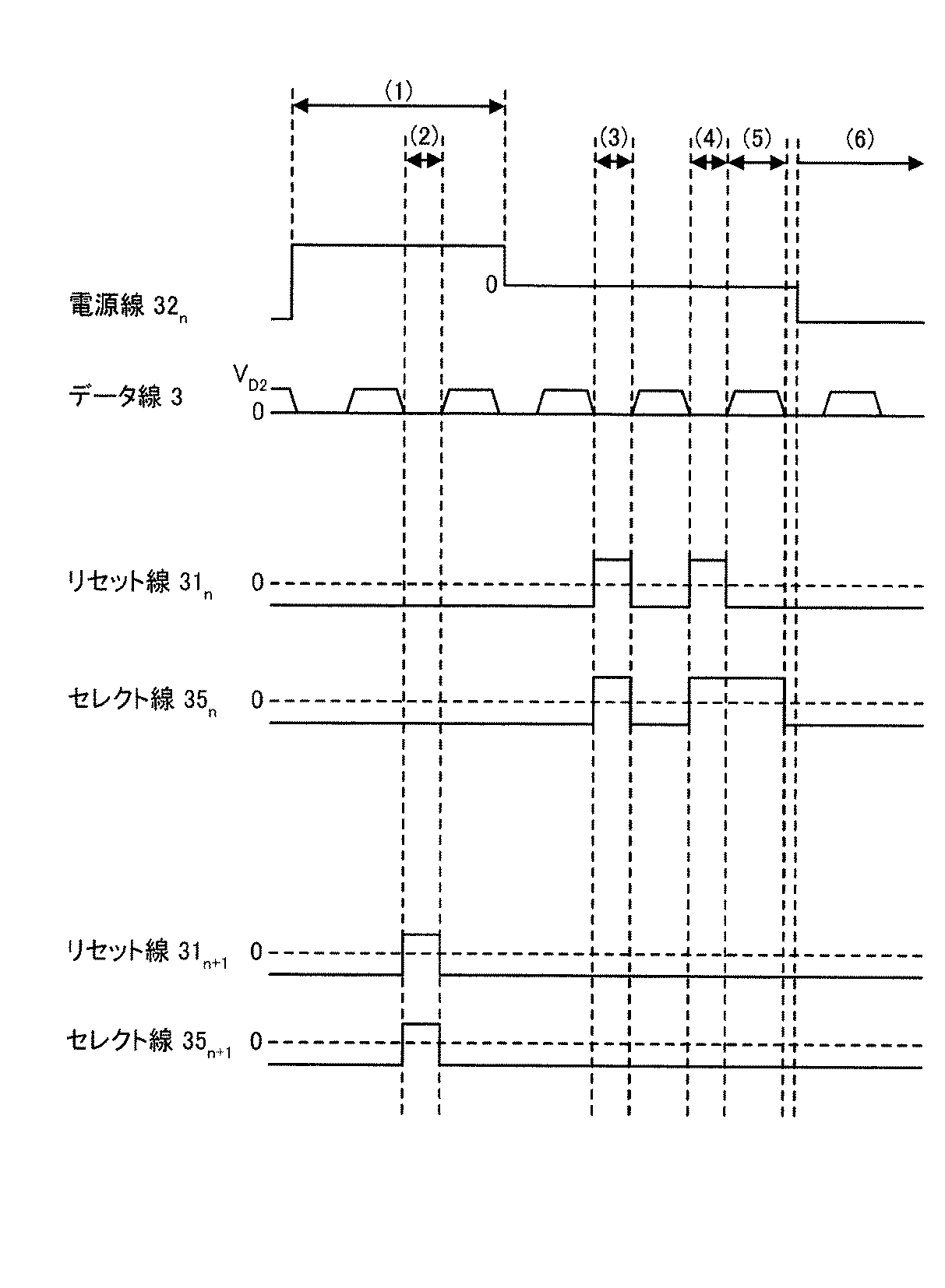
図5は、本実施の形態2にかかる画像表示装置の任意のn段目の画素回路30nと、画素回路30nと同一列に位置し、隣り合う行に配置されたn+1段目の画素回路30n+1との構造を示した図である。図5に示すように、任意の画素回路30nは、実施の形態1と同様に、有機EL素子9nとTFT10nとを有する閾値電圧検出手段A2と、コンデンサ6nと、コンデンサ7nと、ドライバー素子であるTFT8nと、を備える。また、データ線3とTFT4nとを備え、データ線3とTFT4nとは基準電圧書き込み手段A1の構成要素としても機能する。また、TFT10nの駆動状態を制御する第2の走査線であるリセット線31nと、TFT4nの駆動状態を制御する第1の走査線であるセレクト線35nを備える。また、上述した構成要素のうち、データ線3以外の各構成要素は画素回路ごとにそれぞれ備えられている。また、本実施の形態2にかかる画像表示装置は、電源線32nを備え、電源線32nを画素回路30nと画素回路30n+1とが共有する構造を有する。以下、各構成要素について説明する。
【0067】
データ線3にはデータ電圧と0電圧とが交互に印加される。また、TFT4nは、データ線3からのデータ電圧の供給を制御する。さらに、TFT4nは、データ線3が0電圧を印加するタイミングに合わせてオン状態となることによってコンデンサ6nへの0電圧の供給をも制御する。したがって、データ線3は基準電圧の供給源としても機能し、TFT4nはデータ電圧の供給と基準電圧の供給とを制御する第1のスイッチング手段として機能するため、データ線3とTFT4nは基準電圧書き込み手段A1を構成する。なお、TFT4nの駆動状態は、セレクト線35nによって制御される。
【0068】
電源線32nは、発光時に有機EL素子9nと有機EL素子9n+1とに電流を供給するほか、電圧の極性を発光時と比較し反転することによってTFT8nとTFT8n+1とに発光時と逆方向の電流を流す機能を有する。電源線32nの電圧の極性を発光時と比較し反転することによって、白表示を行う画素回路は前処理工程を行い、黒表示を行う画素回路は後述するリセット工程を行う。
【0069】
また、コンデンサ6nとコンデンサ7nとTFT8nとは実施の形態1にかかる画像表示と同様に機能し、有機EL素子9nとTFT10nとは閾値電圧検出手段A2として機能する。また、リセット線31nは、TFT10nの駆動状態を制御する。
【0070】
次に、図6および図7を参照して本実施の形態2にかかる画像表示装置の動作について、画素回路30nが白表示を行い、画素回路30n+1が黒表示を行う場合を例として説明する。画素回路30nは、データ線3に0電圧が印加されるタイミングに合わせて基準電圧書き込み手段A1と閾値電圧検出手段A2とが動作することによって閾値電圧を検出する。
【0071】
図6は、図5に示す画素回路30nと画素回路30n+1のタイミングチャートであり、図7は、図5に示す画素回路30nと画素回路30n+1との動作方法の工程を示す図である。図7(a)は図6の期間(1)、(2)に対応し、図7(b)は図6の期間(3)に対応し、図7(c)は図6の期間(5)に対応し、図7(d)は図6の期間(6)に対応した動作方法を示す図である。なお、図7において、実線部は電流が流れる部分を示し、破線部は電流が流れていない部分を示す。
【0072】
まず、図6と図7(a)を参照して、画素回路30nで行われる前処理工程と画素回路30n+1で行われるリセット工程について説明する。図6の期間(1)に示すように、電源線32nの電圧の極性を発光時と比較し反転し高レベルとすることによって、TFT8nに発光時と逆方向の電流が流れ、有機EL素子9nに正の電荷を蓄積する前処理工程が行われる。その一方、画素回路30n+1では、TFT8n+1に発光時と逆方向の電流を流して有機EL素子9n+1に残存する電荷を取り除くリセット工程を行う。具体的には、画素回路30n+1では、発光時と逆方向の電流が流れ、正の電荷を有機EL素子9n+1に供給することによって、前フレームの発光時に有機EL素子9n+1に蓄積された負の電荷を消去する。
【0073】
さらに、図6の期間(2)では、画素回路30n+1では黒データ書き込み工程が行われる。本工程では、データ線3に0電圧が印加されるタイミングに合わせてTFT4n+1とTFT10n+1とをオン状態とする。TFT10n+1がオン状態となりTFT8n+1のゲート電極とドレイン電極とが導通すると、TFT8n+1のゲート電極に接続するコンデンサ7n+1には、有機EL素子9n+1から放出される電子が供給され、負の電荷が蓄積される。また、TFT4n+1はデータ線3に0電圧が印加される際にオン状態となるため、コンデンサ6n+1には0電圧が供給される。この結果、コンデンサ6n+1とコンデンサ7n+1には負の電荷が保持されることから、TFT8n+1のゲート電極には負電圧が印加されることとなる。したがって、図6の期間(6)において電源線32nが低レベルに変化した場合でも、画素回路30n+1は発光せず黒表示を行うことが可能である。また、本工程においてTFT8n+1のゲート電極に負電圧が印加されることによって、TFT8n+1の閾値電圧の変動幅を低減することができる。すなわち、TFT8n+1のゲート電極に長時間に渡って継続して正電圧を印加した場合、TFT8n+1の閾値電圧の変動が進行するが、本工程を行うことによってTFT8n+1の閾値電圧の変動の進行を留めるとともに閾値電圧を回復することができる。なお、画素回路30n+1は、図6の期間(1)の間であってデータ線3に0電圧が印加されている場合であれば、黒データ書き込み工程を複数回行ってもよい。
【0074】
そして、図7(b)を参照して、画素回路30nで行われる閾値電圧検出工程について説明する。図6の期間(3)はデータ線3に0電圧が印加されている期間である。画素回路30nは、データ線3に0電圧が印加されるタイミングに合わせて、リセット線31nとセレクト線35nとを高レベルとしTFT4nとTFT10nとをオン状態とする。この結果、基準電圧書き込み手段A1は、データ線3からTFT4nを介してコンデンサ6nに0電圧を供給する。一方、閾値電圧検出手段A2は、TFT10nをオン状態としTFT8nのゲート電極とドレイン電極とを導通することによってTFT8nの閾値電圧を検出する。なお、図6の期間(4)に示すように、データ線3が0電圧を印加するタイミングに合わせて閾値電圧検出工程を複数回行うことが可能である。
【0075】
そして、画素回路30nでは、図7(c)に示すように、データ線3にデータ電圧VD2が印加されるタイミングに合わせてTFT4nをオン状態とすることによってデータ書き込み工程が行われる。その後、画素回路30nでは、図7(d)に示すように、電源線32nを低レベルにすることによってTFT8nに電流を流して有機EL素子9nを発光させる発光工程を行う。この結果、画素回路30nでは白表示が行われることとなる。その一方、画素回路30n+1では、図6の期間(2)において上述の黒データ書き込み工程が行われたため、TFT8n+1はオフ状態に維持され、黒表示が行われる。その後、画素回路30n+1では白表示を行うために上記した画素回路30nの動作が行われ、移行し、画素回路30nでは黒表示を行うために上記した画素回路30n+1の動作が行われることによって、画素回路30nと画素回路30n+1は交互に発光を繰り返す。
【0076】
上述したように、本実施の形態2にかかる画像表示装置では、データ線3に0電圧とデータ電圧VD2とが交互に印加されることを利用し、黒表示が終了し発光工程が開始するまでの期間、データ線3に0電圧が印加されるタイミングに合わせて閾値電圧検出工程を行う。このため、発光時間を短縮することなく白表示を行う画素回路の閾値電圧を検出することができる。したがって、リフレッシュレートの最適値の保持とドライバー素子の閾値電圧の変動の補償が可能となる。
【0077】
また、データ線3とTFT4nとは基準電圧書き込み手段A1として機能するため、実施の形態1にかかる画像表示装置が有するTFT13を別個に備える必要がなく、画素回路に備えるTFTの個数を減らすことができる。
【0078】
また、図5に示すように、画素回路30nと画素回路30n+1とは電源線32nを共有する。したがって、本実施の形態2にかかる画像表示装置は、4本の走査線を必要とする実施の形態1にかかる画像表示装置と比較し、各画素回路の走査線を3.5本に減少することができる。
【0079】
また、図6の期間(1)では、図7(a)に示すように、黒表示を行う画素回路30n+1ではリセット工程が行われる。リセット工程を行うのは以下の理由に基づく。すなわち、前フレームの発光工程において、有機EL素子9n+1には、順方向に電流が流れるにしたがって電荷が蓄積される。この電荷が残存したままである場合、発光工程において所定の電流が有機EL素子9n+1に流れた場合であっても、残存した電荷が電流の一部として流れることとなり、その分だけ有機EL素子9n+1中を流れる電流値が減少し、発光輝度が低下する。このため、本実施の形態2にかかる画像表示装置は、黒表示を行う画素回路30n+1についてリセット工程を行い、発光時と逆方向の電流を流すことによって残存する電荷を消去している。したがって、画素回路30n+1が白表示を行う際には、有機EL素子9n+1は前フレーム時に蓄積された電荷の影響を受けることなく所望の輝度で発光することができる。
【0080】
また、閾値電圧検出工程は図6の期間(3)のほか、期間(4)にも行ってもよい。すなわち、前処理工程が終了しデータ書き込み工程が開始するまでの間であって、データ線3に0電圧が印加されている場合であれば、閾値電圧検出工程を複数回行うことが可能である。このため、閾値電圧の検出を長時間行うことが可能となり、TFT8nの閾値電圧を精度よく検出することができる。
【0081】
なお、本実施の形態2にかかる画像表示装置は、電源線32nがTFT8nとTFT8n+1とのソース電極に接続する構造のほか、図8に示すように、電源線42nが有機EL素子9nと有機EL素子9n+1とのアノード側に接続する構造としてもよい。この場合、電源線42nには、図6に示す電源線32nに印加される電圧と逆の極性を示す電圧が印加される。
【0082】
(実施の形態3)
つぎに、実施の形態3にかかる画像表示装置について説明する。本実施の形態3にかかる画像表示装置は、第1のスイッチング手段であるTFTと、隣り合う画素回路の第2のスイッチング手段であるTFTとを1本のセレクト線で制御しており、使用する走査線の本数を減少させた構造を有する。
【0083】
図9は、本実施の形態3にかかる画像表示装置の任意のn段目の画素回路50nと、画素回路50nと同一列に位置し、隣り合う行に配置されたn+1段目の画素回路50n+1との構造を示す図である。図9に示すように、画素回路50nのTFT4nと画素回路50n+1のTFT10n+1とはともに、第3の走査線であるセレクト線55nに接続される。したがって、セレクト線55nが高レベルとなることによって、画素回路50nのTFT4nと画素回路50n+1のTFT10n+1とは同じタイミングでオン状態となる。また、画素回路50nのTFT10nの駆動状態はセレクト線55n-1によって制御される。なお、電源線52nは、実施の形態2における電源線32nと同様に機能する。
【0084】
つぎに、図10および図11を参照して、本実施の形態3にかかる画像表示装置の動作のうち、画素回路50nが白表示を行い、画素回路50n+1が黒表示を行う場合について説明する。
【0085】
図10は図9に示す画素回路50nと画素回路50n+1のタイミングチャートであり、図11は図10に示す画素回路50nと画素回路50n+1との動作方法の工程を示す図である。また、図11(a)は図10に示す期間(1)に対応し、図11(b)は図10に示す期間(2)に対応し、図11(c)は図10に示す期間(3)に対応し、図11(d)は図10に示す期間(4)に対応し、図11(e)は図10に示す期間(5)に対応した動作方法を示す図である。なお、図11では、実線部は電流が流れる部分を示し、破線部は電流が流れていない部分を示す。
【0086】
図11(a)に示すように、図10の期間(1)では、電源線52nに発光時と逆の極性の電圧を印加し高レベルとすることによって、画素回路50nにおいて前処理工程が行われ、画素回路50n+1ではリセット工程が行われる。その後、セレクト線55n-1が高レベルとなり画素回路50nの閾値電圧検出手段A2を構成するTFT10nがオン状態となった後、電源線52nは0レベルになる。
【0087】
つぎに、図10の期間(2)では、画素回路50nにおいて閾値電圧検出工程が行われる。基準電圧書き込み手段A1を構成するデータ線3に0電圧が印加されるタイミングに合わせて、セレクト線55nが高レベルとなる。このとき、図11(b)に示すように、画素回路50nでは、TFT4nがオン状態となることによって基準電圧書き込み手段A1がコンデンサ6nに0電圧を供給し、閾値電圧検出手段A2が閾値電圧検出工程を行う。そして、セレクト線55n-1が低レベルとなりTFT10nがオフ状態となることによって閾値電圧検出工程は終了する。なお、セレクト線55nは高レベルのままであるためTFT4nはオン状態を維持する。
【0088】
つぎに、図10の期間(3)では、画素回路50nにおいてデータ書き込み工程が行われる。すなわち、図10の期間(3)ではデータ線3の印加電圧はデータ電圧VD3に変化し、図11(c)に示すように、画素回路50nではオン状態を維持するTFT4nを介してデータ線3からコンデンサ6nにデータ電圧VD3が供給される。その後、セレクト線55nが低レベルとなりTFT4nがオフ状態となることによって、画素回路50nのデータ書き込み工程は終了する。
【0089】
その後、図10の期間(4)ではデータ線3に0電圧が印加され、画素回路50n+1において黒データ書き込み工程が行われる。図11(d)に示すように、画素回路50n+1ではTFT4n+1のオン状態が維持されているため、データ線3からコンデンサ6n+1に0電圧が供給される。
【0090】
そして、図10の期間(5)では、電源線52nが低レベルとなることによって画素回路50nはTFT8nに電流を流し発光工程を行う。一方、画素回路50n+1は黒表示を行う。
【0091】
上述したように、本実施の形態3にかかる画像表示装置は、実施の形態2にかかる画像表示装置と同様の効果を奏するほか、画素回路50nのTFT4nと画素回路50n+1のTFT10n+1とを単一のセレクト線55nで制御することによって走査線の本数を減少させることができる。また、セレクト線55nに流れる電流はTFT4nとTFT10n+1との駆動状態を制御できる程度であればよいため、セレクト線55nの配線幅を大きくする必要もない。したがって、本実施の形態3にかかる画像表示装置は、3.5本の走査線を必要とする実施の形態2にかかる画像表示装置と比較し、各画素回路の走査線を2.5本に減少させることができる。
【0092】
なお、本実施の形態3にかかる画像表示装置は、図9に示すように電源線52nがTFT8nとTFT8n+1とのソース電極に接続する構造のほか、図12に示すように、共有する電源線62nが有機EL素子9nと有機EL素子9n+1のアノード側に接続する構造としてもよい。この場合、電源線62nには、図10に示す電源線52nに印加される電圧と逆の極性を示す電圧が印加される。
【0093】
(実施の形態4)
つぎに、実施の形態4にかかる画像表示装置について説明する。上述した実施の形態2および実施の形態3では画素回路が発光工程を終了した後に、次に発光する画素回路において前処理工程が行われる構成としたが、実施の形態4では、画素回路において発光工程が行われている間に、次に発光する画素回路において前処理工程を行う構成としている。
【0094】
図13は、本実施の形態4にかかる画像表示装置の任意のn段目の画素回路70nと、画素回路70nと同一列に位置し、隣り合う行に配置されたn+1段目の画素回路70n+1との構造を示す図である。図13に示すように、本実施の形態4にかかる画像表示装置は、画素回路ごとに、リセット線71n、電源線72n、セレクト線75nをそれぞれ備える構造を有する。
【0095】
リセット線71nは画素回路70nに備わるTFT10nの駆動状態を制御する。また、セレクト線75nは画素回路70nに備わるTFT4nの駆動状態を制御する。
【0096】
電源線72nは、画素回路70nの有機EL素子9nのアノード側に接続され、電源線72nと画素回路70n+1に備わる電源線72n+1と間に電位差が生じることによって有機EL素子9nに所定の方向の電流が流れる。具体的には、電源線72nへの印加電圧が電源線72n+1への印加電圧よりも高い場合には、TFT8nにドレイン電極からソース電極に電流が流れ有機EL素子9nは発光する。一方、電源線72nへの印加電圧が電源線72n+1への印加電圧よりも低い場合には、TFT8nにはソース電極からドレイン電極に電流が流れ有機EL素子9nには電荷が蓄積される。
【0097】
つぎに、図14および図15を参照して、本実施の形態4にかかる画像表示装置の動作のうち、画素回路70nが白表示を行い、画素回路70n+1が黒表示を行う場合について説明する。本実施の形態3にかかる画像表示装置では、白表示を行う画素回路が発光工程を行う間、次に発光する画素回路が前処理工程を行っている。
【0098】
図14は、図13に示す画素回路70nと画素回路70n+1のタイミングチャートである。また、図15は、画素回路70nと画素回路70n+1との動作方法の工程を示す図である。図15(a)は図14の期間(1)に対応し、図15(b)は図14の期間(2)に対応し、図15(c)は図14の期間(5)に対応して画素回路70nと画素回路70n+1の動作方法を示す図である。なお、図15では、実線部は電流が流れる部分を示し、破線部は電流が流れていない部分を示す。
【0099】
図14および図15(a)を参照して、画素回路70n+1が発光工程を行う間、次に白表示を行う画素回路70nが前処理工程を行う状態について説明する。図14に示すように期間(1)では、画素回路70n+1は、電源線72n+1を高レベルとすることによってTFT8n+1のドレイン電極からソース電極に向かって電流を流し有機EL素子9n+1を発光させる発光工程を行う。その一方、画素回路70nでは、電源線72nは0レベルを維持するためTFT8nにはソース電極からドレイン電極に向かって電流が流れ、有機EL素子9nには発光時と逆方向の電流が流れ込む。このため、画素回路70nは、有機EL素子9nに電荷が蓄積される前処理工程を行うこととなる。
【0100】
その後、図14の期間(2)では、図15(b)に示すように、画素回路70nが閾値電圧検出工程を行う。なお、図14の期間(3)と期間(4)に示すように、データ線3に0電圧が印加されるタイミングに合わせてセレクト線75nとリセット線71nを高レベルとすることによって、閾値電圧検出工程を複数回行うことが可能である。
【0101】
つぎに、図14の期間(5)では、図15(c)に示すように、データ線3にデータ電圧VD4が印加される期間セレクト線75nを高レベルに維持することによって、画素回路70nがデータ書き込み工程を行う。
【0102】
そして、図14の期間(6)では、画素回路70nは電源線72nを高レベルにすることによってTFT8nに電流を流し発光工程を行う。その一方、画素回路70n+1には発光工程の際に流れる電流と逆方向の電流が流れるため、有機EL素子9n+1は発光せず黒表示を行う。また、有機EL素子9n+1に発光時と逆方向の電流が流れ込むため、画素回路70n+1は前処理工程を行う。さらに、図14の期間(7)では、画素回路70n+1はTFT4n+1とTFT10n+1とをオン状態とすることによってリセット工程を行う。TFT10n+1がオン状態となることによって、TFT8n+1のゲート電極とドレイン電極とが導通し、TFT8n+1のゲート電極に接続するコンデンサ7n+1に負の電荷が蓄積される。また、TFT4n+1がオン状態となるため、コンデンサ6n+1にはデータ線3から0電圧が供給される。このため、前フレームから残存する電荷は消去される。
【0103】
上述したように、本実施の形態4にかかる画像表示装置は、画素回路の発光工程と、次に白表示を行う画素回路の前処理工程を同時に行うことができる。このため、発光時間を短縮することなく閾値電圧検出工程を行う時間を長時間確保することができ、閾値電圧の検出を精度よく行うことができる。したがって、リフレッシュレートの最適値の保持と、閾値電圧の変動の精度の高い補償を可能とし、長期に渡って高品位の画像表示を可能とする画像表示装置を実現することができる。
【0104】
また、黒表示を行う画素回路70n+1は、リセット工程を行うことによって、コンデンサ6n+1とコンデンサ7n+1とに前フレームから残存する電荷を消去することができる。このため、白表示を行う画素回路の有機EL素子は、前フレームの影響を受けることなく所望の輝度で発光することができる。
【0105】
【発明の効果】
以上説明したように、この発明によれば、基準電圧書き込み手段と閾値電圧検出手段とを備えることによって、リフレッシュレートの低下を抑制し、高品位の画像表示を行う画像表示装置を得ることができる。
【図面の簡単な説明】
【図1】実施の形態1における画素回路の構造を示した図である。
【図2】図1に示す画素回路のタイミングチャートである。
【図3】図3(a)〜(d)は、図1に示す画素回路の動作方法の工程を示す図である。
【図4】実施の形態1における画素回路の構造の他の例を示した図である。
【図5】本実施の形態2にかかる画像表示装置の任意のn段目の画素回路と、n段目の画素回路と同一列に位置し、隣り合う行に配置されたn+1段目の画素回路の構造を示した図である。
【図6】図5に示す画素回路のタイミングチャートである。
【図7】図5に示す画素回路の動作方法の工程を示す図である。
【図8】実施の形態2における画素回路の構造の他の例を示した図である。
【図9】本実施の形態3にかかる画像表示装置の任意のn段目の画素回路と、n段目の画素回路と同一列に位置し、隣り合う行に配置されたn+1段目の画素回路の構造を示した図である。
【図10】図9に示す画素回路のタイミングチャートである。
【図11】図9に示す画素回路の動作方法の工程を示す図である。
【図12】実施の形態3における画素回路の構造の他の例を示した図である。
【図13】本実施の形態4にかかる画像表示装置の任意のn段目の画素回路と、n段目の画素回路と同一列に位置し、隣り合う行に配置されたn+1段目の画素回路の構造を示した図である。
【図14】図13に示す画素回路のタイミングチャートである。
【図15】図13に示す画素回路の動作方法の工程を示す図である。
【図16】従来技術における画素回路の構造を示した図である。
【図17】図16に示す画素回路の動作方法の工程を示す図である。
【符号の説明】
A1 基準電圧書き込み手段
A2 閾値電圧検出手段
1、21 画素回路
3 データ線
4、4n、4n+1 TFT
5 セレクト線
6、6n、6n+1 コンデンサ
7、7n、7n+1 コンデンサ
8、8n、8n+1 TFT
9、9n、9n+1 有機EL素子
10、10n、10n+1 TFT
11、31n、31n+1、71n、71n+1、 リセット線
12、22 電源線
13 TFT
32n、42n、52n、62n 電源線
72n、72n+1、72n+2 電源線
30n、40n、50n、60n、70n 画素回路
30n+1、40n+1、50n+1、60n+1、70n+1 画素回路
35n、35n+1、55n-1、55n、55n+1 セレクト線
75n、75n+1 セレクト線
310 データ線
320 セレクト線
330 リセット線
340 マージ線
350、355 コンデンサ
360、365、370、375 TFT
380 有機EL素子[0001]
BACKGROUND OF THE INVENTION
The present invention relates to an active matrix display device in which the luminance of a current light emitting element is controlled, and more particularly to an image display device that suppresses a decrease in refresh rate and displays a high-quality image.
[0002]
[Prior art]
An organic EL display device using an organic electroluminescence (EL) element that emits light by itself does not require a backlight necessary for a liquid crystal display device and is optimal for thinning the device, and there is no restriction on the viewing angle. Practical use is expected as a next-generation image display device. An organic EL element used in an organic EL display device is different from a liquid crystal display device or the like in which a liquid crystal cell is controlled by a voltage in that it is controlled by a current value through which the luminance of each light emitting element flows.
[0003]
In the organic EL display device, a simple (passive) matrix type and an active matrix type can be adopted as a driving method. Although the former has a simple structure, there is a problem that it is difficult to realize a large and high-definition display. Therefore, in recent years, an active matrix type image display device has been developed in which a current flowing through a light emitting element in a pixel is controlled by a driver element having a driving element such as a thin film transistor (TFT) provided in the pixel. It is actively done.
[0004]
The driver element is directly connected to the organic EL element. When the image display is performed, the driver element is turned on to supply current to the organic EL element to cause the organic EL element to emit light. For this reason, when the threshold voltage of the TFT provided in the driver element is changed after using the image display device for a long time, even if the voltage supplied to the inside of the pixel is the same, the current flowing through the driver element changes and the organic The current flowing through the EL element also varies. Therefore, the light emission luminance of the organic EL element becomes non-uniform and the quality of the display image is lowered, which is not appropriate.
[0005]
Therefore, there is a need for an image display device that includes a compensation circuit that compensates for variations in the threshold voltage of the driver element. FIG. 16 is a diagram illustrating a pixel circuit in an image display device including a conventional compensation circuit. As shown in FIG. 16, the conventional image display apparatus includes a
[0006]
Next, an operation method of the pixel circuit until the
[0007]
FIG. 17A is a diagram illustrating a zero voltage application process. The voltage applied to the
[0008]
Then, the process proceeds to a step of detecting the threshold voltage of the
[0009]
Then, the process proceeds to the data writing process shown in FIG. In this case, the voltage applied to the
[0010]
[Patent Document 1]
US Pat. No. 6,229,506 (FIG. 3)
[0011]
[Problems to be solved by the invention]
However, the pixel circuit shown in FIG. 16 has a problem that the time required for displaying one screen becomes long and the refresh rate, which is the number of times the screen is displayed per second, is lowered. The decrease in the refresh rate is caused by the
[0012]
In order to stably detect the threshold voltage, the
[0013]
Further, in the pixel circuit far from the data driver, when the voltage applied to the
[0014]
In the image display device according to the prior art, in order to start the threshold voltage detection process and the data writing process, it is necessary to consider a period during which the applied voltage of the
[0015]
The present invention has been made in view of the above-mentioned problems of the prior art, and an object of the present invention is to obtain an image display device that displays high-quality images without reducing the refresh rate.
[0016]
Means to be Solved by the Invention
In order to solve the above-described problems and achieve the object, the image display device according to
[0017]
According to the image display device of the first aspect, since the reference voltage supply source is provided separately from the data line, it is not necessary to change the voltage applied to the data line. For this reason, it is not necessary to consider the time during which the voltage applied to the data line is stabilized, the time until the data writing process is completed can be shortened, and the decrease in the refresh rate can be suppressed. . Furthermore, since it is possible to compensate for fluctuations in the threshold voltage of the driver element, it is possible to provide a high-quality image display device with uniform light emission luminance.
[0018]
According to a second aspect of the present invention, in the above invention, the third switching unit is turned on while the reference voltage is supplied to the second electrode of the first capacitor. Organic EL The driver element is turned on based on the gate-source voltage generated due to the charge accumulated in the element, and then the current due to the current flowing between the drain and source of the driver element Organic EL The threshold voltage of the driver element is detected when the gate-source voltage decreases to a threshold voltage due to a decrease in the charge of the element and the driver element is turned off.
[0019]
According to a third aspect of the present invention, in the above invention, the data line supplies the first capacitor with a voltage determined based on light emission luminance after the threshold voltage is detected by the threshold voltage detector. It is characterized by doing.
[0020]
According to a fourth aspect of the present invention, in the above invention, the image display device further includes a second capacitor having an electrode electrically connected to the first electrode of the first capacitor and the gate electrode of the driver element. It is characterized by.
[0021]
The image display apparatus according to
[0023]
[0032]
DETAILED DESCRIPTION OF THE INVENTION
Embodiments of an image display apparatus according to the present invention will be described below in detail with reference to the drawings. Note that the present invention is not limited to the embodiments.
[0033]
(Embodiment 1)
First, a first embodiment of the present invention will be described. In the first embodiment, a preprocessing step, a threshold voltage detection step of detecting a threshold voltage of a driver element by writing a reference voltage by reference voltage writing means provided separately from the data line and the first switching means, Image display is performed by repeating a data writing process for writing the data voltage and a light emitting process for supplying a current corresponding to the data voltage to the current light emitting element to emit light.
[0034]
FIG. 1 is a diagram illustrating a structure of a pixel circuit in the first embodiment. The image display apparatus according to the first embodiment is configured by arranging the pixel circuits shown in FIG. 1 in a matrix.
[0035]
As shown in FIG. 1, the pixel circuit according to the first embodiment includes a
[0036]
The
[0037]
The
[0038]
The
[0039]
Further, the reference voltage writing means A1 has a function of supplying 0 voltage that is a predetermined reference voltage to the
[0040]
The threshold voltage detection means A2 detects the threshold voltage of the
[0041]
The
[0042]
The
[0043]
Next, a preprocessing process, a threshold voltage detection process, a data writing process, and a light emitting process will be described as operations of the image display apparatus according to the first embodiment. Here, the threshold voltage detection step is performed by the operation of the reference voltage writing unit A1 and the threshold voltage detection unit A2. FIG. 2 is a timing chart of the pixel circuit shown in FIG. 1, and FIGS. 3A to 3D are diagrams showing steps of an operation method of the pixel circuit shown in FIG. Specifically, FIG. 3A shows a pretreatment process corresponding to the period (1) in FIG. 2, FIG. 3B shows a threshold voltage detection process corresponding to the period (2) in FIG. 3C shows a data writing process corresponding to the period (3) in FIG. 2, and FIG. 3D shows a light emitting process corresponding to the period (4) in FIG. In FIG. 3, the solid line portion indicates a portion where current flows, and the broken line portion indicates a portion where current does not flow. The direction in which the current flows is indicated by an arrow.
[0044]
First, the pretreatment process will be described with reference to FIG. 2 and FIG. The pre-processing step is a step of causing the
[0045]
Next, the threshold voltage detection process will be described. In the threshold voltage detection step, the reference voltage writing means A1 supplies 0 voltage, which is a predetermined reference voltage, to the
[0046]
As shown in FIGS. 2 and 3B, in the threshold voltage detection step, the
[0047]
On the other hand, the threshold voltage detector A2 conducts the gate electrode and the drain electrode of the
[0048]
Next, the data writing process will be described. In the data writing process, the data voltage V is supplied from the
[0049]
As shown in FIGS. 2 and 3C, in the data writing process, the data voltage V is applied to the
[0050]
Next, the light emitting process will be described. In the light emitting process, a current flows through the
[0051]
As shown in FIGS. 2 and 3D, in the light emitting process, the applied voltage of the
[0052]
Next, advantages of the image display apparatus according to the first embodiment will be described. First, the image display apparatus according to the first embodiment can compensate for variations in the threshold voltage by including the threshold voltage detection unit A2. For this reason, the value of the current flowing into the
[0053]
[Formula 1]
[0054]
[Formula 2]
[0055]
From the above, the value of the current flowing through the
[0056]
The image display apparatus according to the first embodiment includes reference voltage writing means A1 provided separately from the
[0057]
Furthermore, since the reference voltage is supplied by the reference voltage writing means A1, the
[0058]
Further, in order to detect the threshold voltage stably, it is necessary that 0 voltage is supplied to the
[0059]
Furthermore, since the image display apparatus according to the first embodiment can delete the time required for stabilizing the applied voltage of the
[0060]
Further, the timing of proceeding from the data writing process to the light emitting process and the timing of proceeding from the light emitting process to the pretreatment process can be arbitrarily controlled by adjusting the level of the voltage applied to the
[0061]
Note that the above-described pixel circuit uses the
[0062]
In the image display apparatus according to the first embodiment, the
[0063]
In the first embodiment, the predetermined reference voltage is described as 0 voltage. However, the voltage is not limited to 0 voltage, and may be a value lower than the voltage value corresponding to the light emission luminance of the
[0064]
(Embodiment 2)
Next, an image display apparatus according to the second embodiment will be described. In the first embodiment described above, it is possible to implement either the progressive method or the interlace method, but in the second embodiment, an image is displayed by using the interlace method.
[0065]
In the interlace method, for example, the even-numbered pixel circuit does not emit light (hereinafter “black display”) while the odd-numbered pixel circuit performs display corresponding to the video signal (hereinafter referred to as “white display”). In other words, the even-numbered pixel circuit performs white display and the odd-numbered pixel circuit performs black display to perform one display. That is, a single screen is displayed by alternately displaying the screens at odd and even levels. In this interlace method, a data voltage supplied to a pixel circuit for performing white display and a 0 voltage supplied to a pixel circuit for performing black display are alternately applied to a data line over a plurality of times during a single display period. Apply. In the second embodiment, the threshold voltage of the driver element is detected using the 0 voltage applied to the data line as the reference voltage.
[0066]
FIG. 5 shows an arbitrary n-
[0067]
A data voltage and a zero voltage are alternately applied to the
[0068]
[0069]
[0070]
Next, with reference to FIG. 6 and FIG. 7, the
[0071]
6 shows the
[0072]
First, referring to FIG. 6 and FIG. n And pre-processing steps performed in the
[0073]
Further, in the period (2) of FIG. n + 1 Then, a black data writing process is performed. In this step, the
[0074]
Then, referring to FIG. 7B, the
[0075]
Then, the
[0076]
As described above, in the image display apparatus according to the second embodiment, the 0 voltage and the data voltage V are applied to the
[0077]
Also, the
[0078]
Further, as shown in FIG. n And
[0079]
Further, in the period (1) in FIG. 6, as shown in FIG. 7A, the
[0080]
Further, the threshold voltage detection step may be performed not only in the period (3) in FIG. 6 but also in the period (4). That is, the threshold voltage detection process can be performed a plurality of times as long as the zero voltage is applied to the
[0081]
Note that the image display apparatus according to the second embodiment has the
[0082]
(Embodiment 3)
Next, an image display apparatus according to the third embodiment will be described. The image display apparatus according to the third embodiment uses a TFT that is a first switching means and a TFT that is a second switching means of an adjacent pixel circuit by using one select line. It has a structure in which the number of scanning lines is reduced.
[0083]
FIG. 9 shows an arbitrary n-th
[0084]
Next, with reference to FIG. 10 and FIG. 11, the
[0085]
10 shows the
[0086]
As shown in FIG. 11A, in the period (1) of FIG. n By applying a voltage having the opposite polarity to that during light emission to a high level, the pixel circuit 50 n A pre-processing step is performed in the
[0087]
Next, in the period (2) of FIG. n A threshold voltage detection step is performed at. The
[0088]
Next, in the period (3) of FIG. n A data writing step is performed. That is, in the period (3) of FIG. 10, the applied voltage of the
[0089]
Thereafter, in the period (4) of FIG. 10, a zero voltage is applied to the
[0090]
In the period (5) of FIG. n Becomes a low level, thereby causing the
[0091]
As described above, the image display device according to the third embodiment has the same effects as the image display device according to the second embodiment, and the
[0092]
The image display apparatus according to the third embodiment has a
[0093]
(Embodiment 4)
Next, an image display apparatus according to
[0094]
FIG. 13 shows an arbitrary n-
[0095]
[0096]
[0097]
Next, with reference to FIGS. 14 and 15, the
[0098]
14 shows the
[0099]
Referring to FIGS. 14 and 15A, the
[0100]
Thereafter, in the period (2) of FIG. 14, as shown in FIG. n Performs the threshold voltage detection step. As shown in period (3) and period (4) of FIG. 14,
[0101]
Next, in the period (5) of FIG. 14, the data voltage V is applied to the
[0102]
Then, in the period (6) of FIG. n Is the
[0103]
As described above, the image display apparatus according to the fourth embodiment can simultaneously perform the light emission process of the pixel circuit and the preprocessing process of the pixel circuit that performs white display next. For this reason, the time for performing the threshold voltage detection step can be secured for a long time without reducing the light emission time, and the threshold voltage can be detected with high accuracy. Therefore, it is possible to realize an image display device that can maintain the optimum value of the refresh rate and highly accurately compensate for fluctuations in the threshold voltage, and can display a high-quality image over a long period of time.
[0104]
Further, the
[0105]
【The invention's effect】
As described above, according to the present invention, by providing the reference voltage writing unit and the threshold voltage detection unit, it is possible to obtain an image display device that suppresses a decrease in the refresh rate and displays a high-quality image. .
[Brief description of the drawings]
FIG. 1 is a diagram showing a structure of a pixel circuit in
FIG. 2 is a timing chart of the pixel circuit shown in FIG.
FIGS. 3A to 3D are diagrams showing steps of an operation method of the pixel circuit shown in FIG.
4 is a diagram showing another example of the structure of the pixel circuit in
FIG. 5 is an n + 1-stage pixel circuit that is located in the same column as the n-th stage pixel circuit of the image display device according to the second embodiment and is arranged in an adjacent row; It is the figure which showed the structure of the circuit.
6 is a timing chart of the pixel circuit shown in FIG.
7 is a diagram showing a process of an operation method of the pixel circuit shown in FIG. 5. FIG.
8 is a diagram showing another example of the structure of the pixel circuit in
FIG. 9 is an n + 1-th stage pixel circuit that is positioned in the same column as the n-th stage pixel circuit and arranged in an adjacent row in the image display device according to the third embodiment; It is the figure which showed the structure of the circuit.
10 is a timing chart of the pixel circuit shown in FIG.
11 is a diagram showing a process of an operation method of the pixel circuit shown in FIG. 9. FIG.
12 is a diagram showing another example of the structure of the pixel circuit in
FIG. 13 is an n + 1-th stage pixel circuit that is positioned in the same column as an n-th stage pixel circuit and arranged in an adjacent row in the image display device according to the fourth embodiment; It is the figure which showed the structure of the circuit.
14 is a timing chart of the pixel circuit shown in FIG.
15 is a diagram showing a process of an operation method of the pixel circuit shown in FIG.
FIG. 16 is a diagram showing a structure of a pixel circuit in the prior art.
17 is a diagram showing a process of an operation method of the pixel circuit shown in FIG. 16. FIG.
[Explanation of symbols]
A1 Reference voltage writing means
A2 threshold voltage detection means
1,21 pixel circuit
3 data lines
4, 4 n 4 n + 1 TFT
5 Select line
6, 6 n , 6 n + 1 Capacitor
7, 7 n , 7 n + 1 Capacitor
8, 8 n , 8 n + 1 TFT
9, 9 n , 9 n + 1 Organic EL device
10, 10 n 10 n + 1 TFT
11, 31 n , 31 n + 1 , 71 n , 71 n + 1 , Reset line
12, 22 Power line
13 TFT
32 n , 42 n , 52 n 62 n Power line
72 n , 72 n + 1 , 72 n + 2 Power line
30 n , 40 n , 50 n , 60 n 70 n Pixel circuit
30 n + 1 , 40 n + 1 , 50 n + 1 , 60 n + 1 70 n + 1 Pixel circuit
35 n , 35 n + 1 55 n-1 55 n 55 n + 1 Select line
75 n 75 n + 1 Select line
310 Data line
320 Select line
330 Reset line
340 merge line
350, 355 capacitors
360, 365, 370, 375 TFT
380 Organic EL device
Claims (6)
前記データ線と別に設けられ、前記第1のコンデンサの第2の電極に所定の基準電圧を供給する供給源と、前記供給源と前記第1のコンデンサの第2の電極との電気的な導通を制御する第2のスイッチング手段と、を有する基準電圧書き込み手段と、
前記有機EL素子に、順方向又は逆方向に電位差を与える電源線と、
前記ドライバー素子のゲート電極とドレイン電極との間の電気的な導通を制御する第3のスイッチング手段を有し、該第3のスイッチング手段がオン状態のときに、前記ドライバー素子のドレイン電極に、前記有機EL素子に蓄積された電荷であって、前記有機EL素子が逆方向に電位差を与えられて蓄積された電荷を供給することによって、前記ドライバー素子の閾値電圧を検出する閾値電圧検出手段と、
を備えたことを特徴とする画像表示装置。An organic EL element that emits light with a luminance corresponding to the flowing current, a driver element that controls a current flowing through the organic EL element, a data line that supplies a voltage defined based on the light emission luminance, and a data line that is supplied from the data line A display pixel comprising: first switching means for controlling writing of voltage to be applied; and a first capacitor in which the first electrode is electrically connected to the gate electrode of the driver element and holds the gate voltage of the driver element. In an image display device arranged in a matrix,
A supply source provided separately from the data line and supplying a predetermined reference voltage to the second electrode of the first capacitor, and electrical conduction between the supply source and the second electrode of the first capacitor Second switching means for controlling the reference voltage writing means,
A power supply line for applying a potential difference in the forward direction or the reverse direction to the organic EL element;
A third switching means for controlling electrical continuity between the gate electrode and the drain electrode of the driver element, and when the third switching means is in an ON state , wherein a charge accumulated in the organic EL element, by supplying the organic EL element is accumulated is a potential difference in the opposite direction the charge, and the threshold voltage detection means for detecting the threshold voltage of the driver element ,
An image display device comprising:
Priority Applications (4)
| Application Number | Priority Date | Filing Date | Title |
|---|---|---|---|
| JP2003139478A JP4484451B2 (en) | 2003-05-16 | 2003-05-16 | Image display device |
| TW093113396A TWI239501B (en) | 2003-05-16 | 2004-05-13 | Image display device |
| US10/844,355 US7259737B2 (en) | 2003-05-16 | 2004-05-13 | Image display apparatus controlling brightness of current-controlled light emitting element |
| CNB2004100447153A CN100419833C (en) | 2003-05-16 | 2004-05-17 | image display device |
Applications Claiming Priority (1)
| Application Number | Priority Date | Filing Date | Title |
|---|---|---|---|
| JP2003139478A JP4484451B2 (en) | 2003-05-16 | 2003-05-16 | Image display device |
Publications (2)
| Publication Number | Publication Date |
|---|---|
| JP2004341359A JP2004341359A (en) | 2004-12-02 |
| JP4484451B2 true JP4484451B2 (en) | 2010-06-16 |
Family
ID=33508162
Family Applications (1)
| Application Number | Title | Priority Date | Filing Date |
|---|---|---|---|
| JP2003139478A Expired - Fee Related JP4484451B2 (en) | 2003-05-16 | 2003-05-16 | Image display device |
Country Status (4)
| Country | Link |
|---|---|
| US (1) | US7259737B2 (en) |
| JP (1) | JP4484451B2 (en) |
| CN (1) | CN100419833C (en) |
| TW (1) | TWI239501B (en) |
Cited By (1)
| Publication number | Priority date | Publication date | Assignee | Title |
|---|---|---|---|---|
| KR101834012B1 (en) | 2011-04-13 | 2018-03-02 | 엘지디스플레이 주식회사 | Organic Light Emitting Diode Display Device |
Families Citing this family (180)
| Publication number | Priority date | Publication date | Assignee | Title |
|---|---|---|---|---|
| US7569849B2 (en) | 2001-02-16 | 2009-08-04 | Ignis Innovation Inc. | Pixel driver circuit and pixel circuit having the pixel driver circuit |
| CA2419704A1 (en) | 2003-02-24 | 2004-08-24 | Ignis Innovation Inc. | Method of manufacturing a pixel with organic light-emitting diode |
| JP4734529B2 (en) * | 2003-02-24 | 2011-07-27 | 奇美電子股▲ふん▼有限公司 | Display device |
| JP4062179B2 (en) * | 2003-06-04 | 2008-03-19 | ソニー株式会社 | Pixel circuit, display device, and driving method of pixel circuit |
| JP4636195B2 (en) * | 2003-08-29 | 2011-02-23 | セイコーエプソン株式会社 | Electro-optical device and electronic apparatus |
| CA2443206A1 (en) | 2003-09-23 | 2005-03-23 | Ignis Innovation Inc. | Amoled display backplanes - pixel driver circuits, array architecture, and external compensation |
| JP4687943B2 (en) * | 2004-03-18 | 2011-05-25 | 奇美電子股▲ふん▼有限公司 | Image display device |
| JP4036209B2 (en) | 2004-04-22 | 2008-01-23 | セイコーエプソン株式会社 | Electronic circuit, driving method thereof, electro-optical device, and electronic apparatus |
| JP4815278B2 (en) * | 2004-05-20 | 2011-11-16 | 京セラ株式会社 | Driving method of image display device |
| JP4521400B2 (en) | 2004-05-20 | 2010-08-11 | 京セラ株式会社 | Image display device |
| DE102004028233A1 (en) * | 2004-06-11 | 2005-12-29 | Deutsche Thomson-Brandt Gmbh | Method for controlling and switching an element of a light-emitting display |
| JP4737587B2 (en) * | 2004-06-18 | 2011-08-03 | 奇美電子股▲ふん▼有限公司 | Driving method of display device |
| CA2472671A1 (en) | 2004-06-29 | 2005-12-29 | Ignis Innovation Inc. | Voltage-programming scheme for current-driven amoled displays |
| KR100590068B1 (en) * | 2004-07-28 | 2006-06-14 | 삼성에스디아이 주식회사 | Light emitting display device, display panel and pixel circuit |
| WO2006053424A1 (en) * | 2004-11-16 | 2006-05-26 | Ignis Innovation Inc. | System and driving method for active matrix light emitting device display |
| CA2490858A1 (en) | 2004-12-07 | 2006-06-07 | Ignis Innovation Inc. | Driving method for compensated voltage-programming of amoled displays |
| KR100623813B1 (en) * | 2004-12-10 | 2006-09-19 | 엘지.필립스 엘시디 주식회사 | Organic EL device and driving method thereof |
| US9275579B2 (en) | 2004-12-15 | 2016-03-01 | Ignis Innovation Inc. | System and methods for extraction of threshold and mobility parameters in AMOLED displays |
| US9280933B2 (en) | 2004-12-15 | 2016-03-08 | Ignis Innovation Inc. | System and methods for extraction of threshold and mobility parameters in AMOLED displays |
| US9171500B2 (en) | 2011-05-20 | 2015-10-27 | Ignis Innovation Inc. | System and methods for extraction of parasitic parameters in AMOLED displays |
| US20140111567A1 (en) | 2005-04-12 | 2014-04-24 | Ignis Innovation Inc. | System and method for compensation of non-uniformities in light emitting device displays |
| US9799246B2 (en) | 2011-05-20 | 2017-10-24 | Ignis Innovation Inc. | System and methods for extraction of threshold and mobility parameters in AMOLED displays |
| US10012678B2 (en) | 2004-12-15 | 2018-07-03 | Ignis Innovation Inc. | Method and system for programming, calibrating and/or compensating, and driving an LED display |
| US8576217B2 (en) | 2011-05-20 | 2013-11-05 | Ignis Innovation Inc. | System and methods for extraction of threshold and mobility parameters in AMOLED displays |
| US10013907B2 (en) | 2004-12-15 | 2018-07-03 | Ignis Innovation Inc. | Method and system for programming, calibrating and/or compensating, and driving an LED display |
| JP5128287B2 (en) | 2004-12-15 | 2013-01-23 | イグニス・イノベイション・インコーポレーテッド | Method and system for performing real-time calibration for display arrays |
| KR100805542B1 (en) * | 2004-12-24 | 2008-02-20 | 삼성에스디아이 주식회사 | Light-emitting display device and driving method thereof |
| CA2495726A1 (en) | 2005-01-28 | 2006-07-28 | Ignis Innovation Inc. | Locally referenced voltage programmed pixel for amoled displays |
| CA2496642A1 (en) | 2005-02-10 | 2006-08-10 | Ignis Innovation Inc. | Fast settling time driving method for organic light-emitting diode (oled) displays based on current programming |
| JP5037795B2 (en) * | 2005-03-17 | 2012-10-03 | グローバル・オーエルイーディー・テクノロジー・リミテッド・ライアビリティ・カンパニー | Display device |
| US8681077B2 (en) * | 2005-03-18 | 2014-03-25 | Semiconductor Energy Laboratory Co., Ltd. | Semiconductor device, and display device, driving method and electronic apparatus thereof |
| JP2006293344A (en) * | 2005-03-18 | 2006-10-26 | Semiconductor Energy Lab Co Ltd | Semiconductor device, display, and driving method and electronic apparatus thereof |
| JP4517927B2 (en) * | 2005-04-14 | 2010-08-04 | セイコーエプソン株式会社 | Electro-optical device and electronic apparatus |
| JP5007491B2 (en) * | 2005-04-14 | 2012-08-22 | セイコーエプソン株式会社 | Electro-optical device and electronic apparatus |
| JP2006317696A (en) * | 2005-05-12 | 2006-11-24 | Sony Corp | Pixel circuit, display device, and pixel circuit control method |
| JP4752331B2 (en) * | 2005-05-25 | 2011-08-17 | セイコーエプソン株式会社 | Light emitting device, driving method and driving circuit thereof, and electronic apparatus |
| CN102663977B (en) * | 2005-06-08 | 2015-11-18 | 伊格尼斯创新有限公司 | For driving the method and system of light emitting device display |
| KR101169053B1 (en) | 2005-06-30 | 2012-07-26 | 엘지디스플레이 주식회사 | Organic Light Emitting Diode Display |
| KR100698700B1 (en) * | 2005-08-01 | 2007-03-23 | 삼성에스디아이 주식회사 | Light emitting display |
| CA2518276A1 (en) | 2005-09-13 | 2007-03-13 | Ignis Innovation Inc. | Compensation technique for luminance degradation in electro-luminance devices |
| KR101209055B1 (en) * | 2005-09-30 | 2012-12-06 | 삼성디스플레이 주식회사 | Display device and driving method thereof |
| KR101324756B1 (en) | 2005-10-18 | 2013-11-05 | 가부시키가이샤 한도오따이 에네루기 켄큐쇼 | Display device and driving method thereof |
| JP5245195B2 (en) | 2005-11-14 | 2013-07-24 | ソニー株式会社 | Pixel circuit |
| WO2007063662A1 (en) * | 2005-11-29 | 2007-06-07 | Kyocera Corporation | Image display |
| JP5258160B2 (en) * | 2005-11-30 | 2013-08-07 | エルジー ディスプレイ カンパニー リミテッド | Image display device |
| US9489891B2 (en) | 2006-01-09 | 2016-11-08 | Ignis Innovation Inc. | Method and system for driving an active matrix display circuit |
| US9269322B2 (en) | 2006-01-09 | 2016-02-23 | Ignis Innovation Inc. | Method and system for driving an active matrix display circuit |
| CA2570898C (en) * | 2006-01-09 | 2008-08-05 | Ignis Innovation Inc. | Method and system for driving an active matrix display circuit |
| KR101282399B1 (en) * | 2006-04-04 | 2013-07-04 | 삼성디스플레이 주식회사 | Display device and driving method thereof |
| KR100784014B1 (en) * | 2006-04-17 | 2007-12-07 | 삼성에스디아이 주식회사 | Organic light emitting display device and driving method thereof |
| JP5397219B2 (en) | 2006-04-19 | 2014-01-22 | イグニス・イノベーション・インコーポレイテッド | Stable drive scheme for active matrix display |
| WO2007144976A1 (en) * | 2006-06-15 | 2007-12-21 | Sharp Kabushiki Kaisha | Current drive type display and pixel circuit |
| JP4882536B2 (en) * | 2006-06-19 | 2012-02-22 | セイコーエプソン株式会社 | Electronic circuit and electronic equipment |
| JP4786437B2 (en) * | 2006-06-29 | 2011-10-05 | 京セラ株式会社 | Driving method of image display device |
| CA2556961A1 (en) | 2006-08-15 | 2008-02-15 | Ignis Innovation Inc. | Oled compensation technique based on oled capacitance |
| JP4256888B2 (en) * | 2006-10-13 | 2009-04-22 | 株式会社 日立ディスプレイズ | Display device |
| JP5055963B2 (en) * | 2006-11-13 | 2012-10-24 | ソニー株式会社 | Display device and driving method of display device |
| CN101192373B (en) * | 2006-11-27 | 2012-01-18 | 奇美电子股份有限公司 | Organic light emitting display and its organic light emitting pixel with voltage compensation technology |
| CN101192374B (en) * | 2006-11-27 | 2012-01-11 | 奇美电子股份有限公司 | Organic light-emitting display panel and its voltage-driven organic light-emitting pixels |
| CN101192369B (en) * | 2006-11-30 | 2011-04-27 | 奇晶光电股份有限公司 | A display device and method for driving pixels thereof |
| JP2008192642A (en) * | 2007-01-31 | 2008-08-21 | Tokyo Electron Ltd | Substrate processing equipment |
| TWI444967B (en) * | 2007-06-15 | 2014-07-11 | Panasonic Corp | Image display device |
| US20090040212A1 (en) * | 2007-08-07 | 2009-02-12 | Himax Technologies Limited | Driver and driver circuit for pixel circuit |
| JP4428436B2 (en) | 2007-10-23 | 2010-03-10 | ソニー株式会社 | Display device and electronic device |
| JP5124250B2 (en) * | 2007-11-30 | 2013-01-23 | エルジー ディスプレイ カンパニー リミテッド | Image display device |
| JP2009204978A (en) * | 2008-02-28 | 2009-09-10 | Sony Corp | El display panel module, el display panel, and electronic device |
| CN104299566B (en) | 2008-04-18 | 2017-11-10 | 伊格尼斯创新公司 | System and driving method for light emitting device display |
| KR100962961B1 (en) * | 2008-06-17 | 2010-06-10 | 삼성모바일디스플레이주식회사 | Pixel and organic light emitting display device using same |
| CA2637343A1 (en) | 2008-07-29 | 2010-01-29 | Ignis Innovation Inc. | Improving the display source driver |
| JP5199367B2 (en) | 2008-08-07 | 2013-05-15 | シャープ株式会社 | Display device and driving method thereof |
| JP2010060805A (en) * | 2008-09-03 | 2010-03-18 | Sony Corp | Display device, method for driving the display device, and electronic equipment |
| WO2010041426A1 (en) * | 2008-10-07 | 2010-04-15 | パナソニック株式会社 | Image display device and method for controlling the same |
| KR101282996B1 (en) | 2008-11-15 | 2013-07-04 | 엘지디스플레이 주식회사 | Organic electro-luminescent display device and driving method thereof |
| KR101452210B1 (en) * | 2008-11-17 | 2014-10-23 | 삼성디스플레이 주식회사 | Display device and driving method thereof |
| JP5627175B2 (en) * | 2008-11-28 | 2014-11-19 | エルジー ディスプレイ カンパニー リミテッド | Image display device |
| US9370075B2 (en) | 2008-12-09 | 2016-06-14 | Ignis Innovation Inc. | System and method for fast compensation programming of pixels in a display |
| TW201025244A (en) * | 2008-12-31 | 2010-07-01 | Ind Tech Res Inst | Pixel circuit and method for driving a pixel |
| JP4844634B2 (en) * | 2009-01-06 | 2011-12-28 | ソニー株式会社 | Driving method of organic electroluminescence light emitting unit |
| JP5099069B2 (en) * | 2009-04-24 | 2012-12-12 | ソニー株式会社 | Pixel circuit, pixel circuit driving method, display device, and display device driving method |
| US8847866B2 (en) | 2009-06-12 | 2014-09-30 | Sharp Kabushiki Kaisha | Pixel circuit and display device |
| US8704809B2 (en) * | 2009-06-12 | 2014-04-22 | Sharp Kabushiki Kaisha | Pixel circuit and display device |
| US9311859B2 (en) | 2009-11-30 | 2016-04-12 | Ignis Innovation Inc. | Resetting cycle for aging compensation in AMOLED displays |
| CA2688870A1 (en) | 2009-11-30 | 2011-05-30 | Ignis Innovation Inc. | Methode and techniques for improving display uniformity |
| CA2669367A1 (en) | 2009-06-16 | 2010-12-16 | Ignis Innovation Inc | Compensation technique for color shift in displays |
| US9384698B2 (en) | 2009-11-30 | 2016-07-05 | Ignis Innovation Inc. | System and methods for aging compensation in AMOLED displays |
| US10319307B2 (en) | 2009-06-16 | 2019-06-11 | Ignis Innovation Inc. | Display system with compensation techniques and/or shared level resources |
| JP4998538B2 (en) * | 2009-10-20 | 2012-08-15 | ソニー株式会社 | Display device and electronic device |
| US8283967B2 (en) | 2009-11-12 | 2012-10-09 | Ignis Innovation Inc. | Stable current source for system integration to display substrate |
| US10996258B2 (en) | 2009-11-30 | 2021-05-04 | Ignis Innovation Inc. | Defect detection and correction of pixel circuits for AMOLED displays |
| US8803417B2 (en) | 2009-12-01 | 2014-08-12 | Ignis Innovation Inc. | High resolution pixel architecture |
| CA2687631A1 (en) | 2009-12-06 | 2011-06-06 | Ignis Innovation Inc | Low power driving scheme for display applications |
| TWI401636B (en) * | 2010-01-18 | 2013-07-11 | Ind Tech Res Inst | Pixel unit and display device utilizing the same |
| US20140313111A1 (en) | 2010-02-04 | 2014-10-23 | Ignis Innovation Inc. | System and methods for extracting correlation curves for an organic light emitting device |
| US9881532B2 (en) | 2010-02-04 | 2018-01-30 | Ignis Innovation Inc. | System and method for extracting correlation curves for an organic light emitting device |
| US10176736B2 (en) | 2010-02-04 | 2019-01-08 | Ignis Innovation Inc. | System and methods for extracting correlation curves for an organic light emitting device |
| US10089921B2 (en) | 2010-02-04 | 2018-10-02 | Ignis Innovation Inc. | System and methods for extracting correlation curves for an organic light emitting device |
| CA2692097A1 (en) | 2010-02-04 | 2011-08-04 | Ignis Innovation Inc. | Extracting correlation curves for light emitting device |
| US10163401B2 (en) | 2010-02-04 | 2018-12-25 | Ignis Innovation Inc. | System and methods for extracting correlation curves for an organic light emitting device |
| CA2696778A1 (en) | 2010-03-17 | 2011-09-17 | Ignis Innovation Inc. | Lifetime, uniformity, parameter extraction methods |
| JP2010191454A (en) * | 2010-04-02 | 2010-09-02 | Seiko Epson Corp | Light emitting device, drive method and drive circuit therefor, and electronic equipment |
| JP5565097B2 (en) * | 2010-05-26 | 2014-08-06 | セイコーエプソン株式会社 | Electro-optical device and electronic apparatus |
| JP5565098B2 (en) * | 2010-05-26 | 2014-08-06 | セイコーエプソン株式会社 | Electro-optical device and electronic apparatus |
| JP5655371B2 (en) * | 2010-05-26 | 2015-01-21 | セイコーエプソン株式会社 | Electronic device and driving method thereof |
| KR101762344B1 (en) * | 2010-07-27 | 2017-07-31 | 삼성디스플레이 주식회사 | Organic electroluminescence emitting display device |
| KR101658037B1 (en) * | 2010-11-09 | 2016-09-21 | 삼성전자주식회사 | Method of driving active display device |
| US8907991B2 (en) | 2010-12-02 | 2014-12-09 | Ignis Innovation Inc. | System and methods for thermal compensation in AMOLED displays |
| TWI557711B (en) | 2011-05-12 | 2016-11-11 | 半導體能源研究所股份有限公司 | Display device driving method |
| US9606607B2 (en) | 2011-05-17 | 2017-03-28 | Ignis Innovation Inc. | Systems and methods for display systems with dynamic power control |
| US9886899B2 (en) | 2011-05-17 | 2018-02-06 | Ignis Innovation Inc. | Pixel Circuits for AMOLED displays |
| EP2710578B1 (en) | 2011-05-17 | 2019-04-24 | Ignis Innovation Inc. | Systems and methods for display systems with dynamic power control |
| US9351368B2 (en) | 2013-03-08 | 2016-05-24 | Ignis Innovation Inc. | Pixel circuits for AMOLED displays |
| US20140368491A1 (en) | 2013-03-08 | 2014-12-18 | Ignis Innovation Inc. | Pixel circuits for amoled displays |
| US9530349B2 (en) | 2011-05-20 | 2016-12-27 | Ignis Innovations Inc. | Charged-based compensation and parameter extraction in AMOLED displays |
| US9466240B2 (en) | 2011-05-26 | 2016-10-11 | Ignis Innovation Inc. | Adaptive feedback system for compensating for aging pixel areas with enhanced estimation speed |
| US9773439B2 (en) | 2011-05-27 | 2017-09-26 | Ignis Innovation Inc. | Systems and methods for aging compensation in AMOLED displays |
| EP2945147B1 (en) | 2011-05-28 | 2018-08-01 | Ignis Innovation Inc. | Method for fast compensation programming of pixels in a display |
| TWI441137B (en) | 2011-07-08 | 2014-06-11 | Hannstar Display Corp | Compensation circuit for keeping luminance intensity of diode |
| US9070775B2 (en) | 2011-08-03 | 2015-06-30 | Ignis Innovations Inc. | Thin film transistor |
| US8901579B2 (en) | 2011-08-03 | 2014-12-02 | Ignis Innovation Inc. | Organic light emitting diode and method of manufacturing |
| TWI442374B (en) * | 2011-08-16 | 2014-06-21 | Hannstar Display Corp | Compensation circuit of organic light-emitting diode |
| US12176356B2 (en) | 2011-10-18 | 2024-12-24 | Semiconductor Energy Laboratory Co., Ltd. | Semiconductor device including transistor and light-emitting element |
| KR20190033094A (en) | 2011-10-18 | 2019-03-28 | 가부시키가이샤 한도오따이 에네루기 켄큐쇼 | Method for driving semiconductor device |
| US9324268B2 (en) | 2013-03-15 | 2016-04-26 | Ignis Innovation Inc. | Amoled displays with multiple readout circuits |
| US9385169B2 (en) | 2011-11-29 | 2016-07-05 | Ignis Innovation Inc. | Multi-functional active matrix organic light-emitting diode display |
| US10089924B2 (en) | 2011-11-29 | 2018-10-02 | Ignis Innovation Inc. | Structural and low-frequency non-uniformity compensation |
| US8937632B2 (en) | 2012-02-03 | 2015-01-20 | Ignis Innovation Inc. | Driving system for active-matrix displays |
| US9747834B2 (en) | 2012-05-11 | 2017-08-29 | Ignis Innovation Inc. | Pixel circuits including feedback capacitors and reset capacitors, and display systems therefore |
| US8922544B2 (en) | 2012-05-23 | 2014-12-30 | Ignis Innovation Inc. | Display systems with compensation for line propagation delay |
| US9336717B2 (en) | 2012-12-11 | 2016-05-10 | Ignis Innovation Inc. | Pixel circuits for AMOLED displays |
| US9786223B2 (en) | 2012-12-11 | 2017-10-10 | Ignis Innovation Inc. | Pixel circuits for AMOLED displays |
| US9171504B2 (en) | 2013-01-14 | 2015-10-27 | Ignis Innovation Inc. | Driving scheme for emissive displays providing compensation for driving transistor variations |
| US9830857B2 (en) | 2013-01-14 | 2017-11-28 | Ignis Innovation Inc. | Cleaning common unwanted signals from pixel measurements in emissive displays |
| US9721505B2 (en) | 2013-03-08 | 2017-08-01 | Ignis Innovation Inc. | Pixel circuits for AMOLED displays |
| CA2894717A1 (en) | 2015-06-19 | 2016-12-19 | Ignis Innovation Inc. | Optoelectronic device characterization in array with shared sense line |
| EP3043338A1 (en) | 2013-03-14 | 2016-07-13 | Ignis Innovation Inc. | Re-interpolation with edge detection for extracting an aging pattern for amoled displays |
| DE112014001402T5 (en) | 2013-03-15 | 2016-01-28 | Ignis Innovation Inc. | Dynamic adjustment of touch resolutions of an Amoled display |
| WO2014174427A1 (en) | 2013-04-22 | 2014-10-30 | Ignis Innovation Inc. | Inspection system for oled display panels |
| US9437137B2 (en) | 2013-08-12 | 2016-09-06 | Ignis Innovation Inc. | Compensation accuracy |
| TWI534993B (en) * | 2013-09-25 | 2016-05-21 | 友達光電股份有限公司 | Pixel structure of inorganic light-emitting diode |
| CN103489406B (en) * | 2013-10-08 | 2015-11-25 | 京东方科技集团股份有限公司 | A kind of pixel drive unit and driving method, image element circuit |
| KR102089051B1 (en) | 2013-11-25 | 2020-03-16 | 삼성디스플레이 주식회사 | Pixel circuit for increasing validity of current sensing |
| US9741282B2 (en) | 2013-12-06 | 2017-08-22 | Ignis Innovation Inc. | OLED display system and method |
| US9761170B2 (en) | 2013-12-06 | 2017-09-12 | Ignis Innovation Inc. | Correction for localized phenomena in an image array |
| US9502653B2 (en) | 2013-12-25 | 2016-11-22 | Ignis Innovation Inc. | Electrode contacts |
| US10997901B2 (en) | 2014-02-28 | 2021-05-04 | Ignis Innovation Inc. | Display system |
| JP6363852B2 (en) * | 2014-03-03 | 2018-07-25 | 日本放送協会 | Driving circuit |
| US10176752B2 (en) | 2014-03-24 | 2019-01-08 | Ignis Innovation Inc. | Integrated gate driver |
| US10192479B2 (en) | 2014-04-08 | 2019-01-29 | Ignis Innovation Inc. | Display system using system level resources to calculate compensation parameters for a display module in a portable device |
| CN103971643B (en) * | 2014-05-21 | 2016-01-06 | 上海天马有机发光显示技术有限公司 | A kind of organic light-emitting diode pixel circuit and display device |
| CN105280136B (en) * | 2014-07-10 | 2018-11-30 | 信利半导体有限公司 | A kind of AMOLED pixel circuit and its driving method |
| US9799261B2 (en) | 2014-09-25 | 2017-10-24 | X-Celeprint Limited | Self-compensating circuit for faulty display pixels |
| US9468050B1 (en) * | 2014-09-25 | 2016-10-11 | X-Celeprint Limited | Self-compensating circuit for faulty display pixels |
| KR20160048640A (en) * | 2014-10-23 | 2016-05-04 | 삼성디스플레이 주식회사 | Display apparatus, pixel circuit, and control method of display apparatus |
| CA2872563A1 (en) | 2014-11-28 | 2016-05-28 | Ignis Innovation Inc. | High pixel density array architecture |
| CA2873476A1 (en) | 2014-12-08 | 2016-06-08 | Ignis Innovation Inc. | Smart-pixel display architecture |
| CA2879462A1 (en) | 2015-01-23 | 2016-07-23 | Ignis Innovation Inc. | Compensation for color variation in emissive devices |
| CA2886862A1 (en) | 2015-04-01 | 2016-10-01 | Ignis Innovation Inc. | Adjusting display brightness for avoiding overheating and/or accelerated aging |
| CN104700761B (en) * | 2015-04-03 | 2017-08-29 | 京东方科技集团股份有限公司 | One kind detection circuit and its detection method and drive system |
| CA2889870A1 (en) | 2015-05-04 | 2016-11-04 | Ignis Innovation Inc. | Optical feedback system |
| CA2892714A1 (en) | 2015-05-27 | 2016-11-27 | Ignis Innovation Inc | Memory bandwidth reduction in compensation system |
| KR102455327B1 (en) * | 2015-06-15 | 2022-10-18 | 삼성디스플레이 주식회사 | Display device and method of driving the same |
| US10255834B2 (en) | 2015-07-23 | 2019-04-09 | X-Celeprint Limited | Parallel redundant chiplet system for controlling display pixels |
| US10657895B2 (en) | 2015-07-24 | 2020-05-19 | Ignis Innovation Inc. | Pixels and reference circuits and timing techniques |
| CA2898282A1 (en) | 2015-07-24 | 2017-01-24 | Ignis Innovation Inc. | Hybrid calibration of current sources for current biased voltage progra mmed (cbvp) displays |
| US10373554B2 (en) | 2015-07-24 | 2019-08-06 | Ignis Innovation Inc. | Pixels and reference circuits and timing techniques |
| CA2900170A1 (en) | 2015-08-07 | 2017-02-07 | Gholamreza Chaji | Calibration of pixel based on improved reference values |
| CA2908285A1 (en) | 2015-10-14 | 2017-04-14 | Ignis Innovation Inc. | Driver with multiple color pixel structure |
| CA2909813A1 (en) | 2015-10-26 | 2017-04-26 | Ignis Innovation Inc | High ppi pattern orientation |
| KR102523377B1 (en) * | 2016-07-15 | 2023-04-20 | 삼성디스플레이 주식회사 | Organic light emitting display device and head mounted display system having the same |
| CN106409227A (en) * | 2016-12-02 | 2017-02-15 | 武汉华星光电技术有限公司 | Pixel circuit and driving method thereof, and organic light-emitting display device |
| DE102017222059A1 (en) | 2016-12-06 | 2018-06-07 | Ignis Innovation Inc. | Pixel circuits for reducing hysteresis |
| KR102581190B1 (en) * | 2016-12-14 | 2023-09-21 | 삼성전자주식회사 | Display apparatus and seam correction method thereof |
| US10714018B2 (en) | 2017-05-17 | 2020-07-14 | Ignis Innovation Inc. | System and method for loading image correction data for displays |
| US11025899B2 (en) | 2017-08-11 | 2021-06-01 | Ignis Innovation Inc. | Optical correction systems and methods for correcting non-uniformity of emissive display devices |
| US10971078B2 (en) | 2018-02-12 | 2021-04-06 | Ignis Innovation Inc. | Pixel measurement through data line |
| TWI703547B (en) * | 2019-06-13 | 2020-09-01 | 友達光電股份有限公司 | Pixel compensation circuit |
| CN110544458B (en) * | 2019-09-10 | 2021-08-06 | 京东方科技集团股份有限公司 | A pixel circuit, a driving method thereof, and a display device |
| US11145257B2 (en) * | 2020-02-02 | 2021-10-12 | Novatek Microelectronics Corp. | Display device driving method and related driver circuit |
| KR102811771B1 (en) * | 2021-12-30 | 2025-05-22 | 엘지디스플레이 주식회사 | Power Supply, Light Emitting Display Device and Driving Method thereof |
| CN114664223B (en) * | 2022-03-31 | 2022-11-25 | 惠科股份有限公司 | Driving circuit of display panel, array substrate and driving method of array substrate |
Family Cites Families (25)
| Publication number | Priority date | Publication date | Assignee | Title |
|---|---|---|---|---|
| JP4251377B2 (en) * | 1997-04-23 | 2009-04-08 | 宇東科技股▲ふん▼有限公司 | Active matrix light emitting diode pixel structure and method |
| US6229506B1 (en) | 1997-04-23 | 2001-05-08 | Sarnoff Corporation | Active matrix light emitting diode pixel structure and concomitant method |
| JP5210473B2 (en) * | 1999-06-21 | 2013-06-12 | 株式会社半導体エネルギー研究所 | Display device |
| JP4727029B2 (en) * | 1999-11-29 | 2011-07-20 | 株式会社半導体エネルギー研究所 | EL display device, electric appliance, and semiconductor element substrate for EL display device |
| JP4831889B2 (en) * | 2000-06-22 | 2011-12-07 | 株式会社半導体エネルギー研究所 | Display device |
| ATE524804T1 (en) * | 2000-07-07 | 2011-09-15 | Seiko Epson Corp | CURRENT CONTROLLED ELECTRO-OPTICAL DEVICE, E.G. ELECTROLUMINescent DISPLAY, WITH COMPLEMENTARY CONTROL TRANSISTORS EFFECTIVE AGAINST CHANGES IN THRESHOLD VOLTAGE |
| US7737933B2 (en) * | 2000-09-26 | 2010-06-15 | Toshiba Matsushita Display Technology Co., Ltd. | Display unit and drive system thereof and an information display unit |
| TWI248319B (en) * | 2001-02-08 | 2006-01-21 | Semiconductor Energy Lab | Light emitting device and electronic equipment using the same |
| JP2002278504A (en) * | 2001-03-19 | 2002-09-27 | Mitsubishi Electric Corp | Self-luminous display |
| JP2002351401A (en) * | 2001-03-21 | 2002-12-06 | Mitsubishi Electric Corp | Self-luminous display |
| JP2003150115A (en) * | 2001-08-29 | 2003-05-23 | Seiko Epson Corp | Current generation circuit, semiconductor integrated circuit, electro-optical device, and electronic equipment |
| KR100714513B1 (en) * | 2001-09-07 | 2007-05-07 | 마츠시타 덴끼 산교 가부시키가이샤 | Drive circuit of EL display device, electronic display device and EL display device |
| JP4075505B2 (en) * | 2001-09-10 | 2008-04-16 | セイコーエプソン株式会社 | Electronic circuit, electronic device, and electronic apparatus |
| TW563088B (en) * | 2001-09-17 | 2003-11-21 | Semiconductor Energy Lab | Light emitting device, method of driving a light emitting device, and electronic equipment |
| JP3810725B2 (en) * | 2001-09-21 | 2006-08-16 | 株式会社半導体エネルギー研究所 | LIGHT EMITTING DEVICE AND ELECTRONIC DEVICE |
| SG120888A1 (en) * | 2001-09-28 | 2006-04-26 | Semiconductor Energy Lab | A light emitting device and electronic apparatus using the same |
| JP2003108067A (en) * | 2001-09-28 | 2003-04-11 | Sanyo Electric Co Ltd | Display device |
| SG120889A1 (en) * | 2001-09-28 | 2006-04-26 | Semiconductor Energy Lab | A light emitting device and electronic apparatus using the same |
| US7456810B2 (en) * | 2001-10-26 | 2008-11-25 | Semiconductor Energy Laboratory Co., Ltd. | Light-emitting device and driving method thereof |
| JP2003150107A (en) * | 2001-11-09 | 2003-05-23 | Sharp Corp | Display device and driving method thereof |
| TWI310632B (en) * | 2002-01-17 | 2009-06-01 | Semiconductor Energy Lab | Electric circuit |
| JP3956347B2 (en) * | 2002-02-26 | 2007-08-08 | インターナショナル・ビジネス・マシーンズ・コーポレーション | Display device |
| CN1666242A (en) * | 2002-04-26 | 2005-09-07 | 东芝松下显示技术有限公司 | Driving Circuit for Electroluminescence Display |
| US7053875B2 (en) * | 2004-08-21 | 2006-05-30 | Chen-Jean Chou | Light emitting device display circuit and drive method thereof |
| JP4254675B2 (en) * | 2004-09-29 | 2009-04-15 | カシオ計算機株式会社 | Display panel |
-
2003
- 2003-05-16 JP JP2003139478A patent/JP4484451B2/en not_active Expired - Fee Related
-
2004
- 2004-05-13 TW TW093113396A patent/TWI239501B/en active
- 2004-05-13 US US10/844,355 patent/US7259737B2/en not_active Expired - Lifetime
- 2004-05-17 CN CNB2004100447153A patent/CN100419833C/en not_active Expired - Fee Related
Cited By (1)
| Publication number | Priority date | Publication date | Assignee | Title |
|---|---|---|---|---|
| KR101834012B1 (en) | 2011-04-13 | 2018-03-02 | 엘지디스플레이 주식회사 | Organic Light Emitting Diode Display Device |
Also Published As
| Publication number | Publication date |
|---|---|
| JP2004341359A (en) | 2004-12-02 |
| TWI239501B (en) | 2005-09-11 |
| CN100419833C (en) | 2008-09-17 |
| US7259737B2 (en) | 2007-08-21 |
| US20040252089A1 (en) | 2004-12-16 |
| TW200428338A (en) | 2004-12-16 |
| CN1551084A (en) | 2004-12-01 |
Similar Documents
| Publication | Publication Date | Title |
|---|---|---|
| JP4484451B2 (en) | Image display device | |
| JP4734529B2 (en) | Display device | |
| JP4737587B2 (en) | Driving method of display device | |
| US7483002B2 (en) | Picture image display device and method of driving the same | |
| CN101452670B (en) | Electrooptical device and its drive device | |
| JP6142178B2 (en) | Display device and driving method | |
| US7355571B2 (en) | Display device and its driving method | |
| JP5008412B2 (en) | Image display device and driving method of image display device | |
| US8344975B2 (en) | EL display device with voltage variation reduction transistor | |
| US7808455B2 (en) | Display apparatus | |
| US8223094B2 (en) | Display device and driving method thereof | |
| US7551152B2 (en) | Display and method of driving pixel | |
| CN103946912B (en) | Display device and control method thereof | |
| US20080238901A1 (en) | Display apparatus, display-apparatus driving method and electronic equipment | |
| JP2004361753A (en) | Image display device | |
| WO2020194647A1 (en) | Display device and driving method thereof | |
| CN100380426C (en) | Active Matrix Display Device | |
| CN101816031B (en) | Active matrix type display panel, display device, and drive method | |
| JP4501059B2 (en) | Pixel circuit and display device | |
| US20050017930A1 (en) | Image display apparatus | |
| CN100418123C (en) | display device | |
| JP4797555B2 (en) | Display device and driving method thereof | |
| JP4962682B2 (en) | Light emission drive circuit and display device | |
| US20140218270A1 (en) | Display device, driving method of display device, and electronic apparatus | |
| CN111971739A (en) | Display device driving method and display device |
Legal Events
| Date | Code | Title | Description |
|---|---|---|---|
| A621 | Written request for application examination |
Free format text: JAPANESE INTERMEDIATE CODE: A621 Effective date: 20051104 |
|
| A131 | Notification of reasons for refusal |
Free format text: JAPANESE INTERMEDIATE CODE: A131 Effective date: 20081209 |
|
| A521 | Request for written amendment filed |
Free format text: JAPANESE INTERMEDIATE CODE: A523 Effective date: 20090304 |
|
| A131 | Notification of reasons for refusal |
Free format text: JAPANESE INTERMEDIATE CODE: A131 Effective date: 20091110 |
|
| A521 | Request for written amendment filed |
Free format text: JAPANESE INTERMEDIATE CODE: A523 Effective date: 20100203 |
|
| TRDD | Decision of grant or rejection written | ||
| A01 | Written decision to grant a patent or to grant a registration (utility model) |
Free format text: JAPANESE INTERMEDIATE CODE: A01 Effective date: 20100302 |
|
| A01 | Written decision to grant a patent or to grant a registration (utility model) |
Free format text: JAPANESE INTERMEDIATE CODE: A01 |
|
| A61 | First payment of annual fees (during grant procedure) |
Free format text: JAPANESE INTERMEDIATE CODE: A61 Effective date: 20100323 |
|
| R150 | Certificate of patent or registration of utility model |
Free format text: JAPANESE INTERMEDIATE CODE: R150 |
|
| FPAY | Renewal fee payment (event date is renewal date of database) |
Free format text: PAYMENT UNTIL: 20130402 Year of fee payment: 3 |
|
| FPAY | Renewal fee payment (event date is renewal date of database) |
Free format text: PAYMENT UNTIL: 20140402 Year of fee payment: 4 |
|
| R250 | Receipt of annual fees |
Free format text: JAPANESE INTERMEDIATE CODE: R250 |
|
| R250 | Receipt of annual fees |
Free format text: JAPANESE INTERMEDIATE CODE: R250 |
|
| S531 | Written request for registration of change of domicile |
Free format text: JAPANESE INTERMEDIATE CODE: R313531 |
|
| S533 | Written request for registration of change of name |
Free format text: JAPANESE INTERMEDIATE CODE: R313533 |
|
| R350 | Written notification of registration of transfer |
Free format text: JAPANESE INTERMEDIATE CODE: R350 |
|
| S111 | Request for change of ownership or part of ownership |
Free format text: JAPANESE INTERMEDIATE CODE: R313117 |
|
| R350 | Written notification of registration of transfer |
Free format text: JAPANESE INTERMEDIATE CODE: R350 |
|
| R250 | Receipt of annual fees |
Free format text: JAPANESE INTERMEDIATE CODE: R250 |
|
| R250 | Receipt of annual fees |
Free format text: JAPANESE INTERMEDIATE CODE: R250 |
|
| LAPS | Cancellation because of no payment of annual fees |