CN110544458B - A pixel circuit, a driving method thereof, and a display device - Google Patents
A pixel circuit, a driving method thereof, and a display device Download PDFInfo
- Publication number
- CN110544458B CN110544458B CN201910852504.9A CN201910852504A CN110544458B CN 110544458 B CN110544458 B CN 110544458B CN 201910852504 A CN201910852504 A CN 201910852504A CN 110544458 B CN110544458 B CN 110544458B
- Authority
- CN
- China
- Prior art keywords
- transistor
- driving transistor
- pole
- signal
- voltage
- Prior art date
- Legal status (The legal status is an assumption and is not a legal conclusion. Google has not performed a legal analysis and makes no representation as to the accuracy of the status listed.)
- Active
Links
Images


Classifications
-
- G—PHYSICS
- G09—EDUCATION; CRYPTOGRAPHY; DISPLAY; ADVERTISING; SEALS
- G09G—ARRANGEMENTS OR CIRCUITS FOR CONTROL OF INDICATING DEVICES USING STATIC MEANS TO PRESENT VARIABLE INFORMATION
- G09G3/00—Control arrangements or circuits, of interest only in connection with visual indicators other than cathode-ray tubes
- G09G3/20—Control arrangements or circuits, of interest only in connection with visual indicators other than cathode-ray tubes for presentation of an assembly of a number of characters, e.g. a page, by composing the assembly by combination of individual elements arranged in a matrix no fixed position being assigned to or needed to be assigned to the individual characters or partial characters
- G09G3/22—Control arrangements or circuits, of interest only in connection with visual indicators other than cathode-ray tubes for presentation of an assembly of a number of characters, e.g. a page, by composing the assembly by combination of individual elements arranged in a matrix no fixed position being assigned to or needed to be assigned to the individual characters or partial characters using controlled light sources
- G09G3/30—Control arrangements or circuits, of interest only in connection with visual indicators other than cathode-ray tubes for presentation of an assembly of a number of characters, e.g. a page, by composing the assembly by combination of individual elements arranged in a matrix no fixed position being assigned to or needed to be assigned to the individual characters or partial characters using controlled light sources using electroluminescent panels
- G09G3/32—Control arrangements or circuits, of interest only in connection with visual indicators other than cathode-ray tubes for presentation of an assembly of a number of characters, e.g. a page, by composing the assembly by combination of individual elements arranged in a matrix no fixed position being assigned to or needed to be assigned to the individual characters or partial characters using controlled light sources using electroluminescent panels semiconductive, e.g. using light-emitting diodes [LED]
- G09G3/3208—Control arrangements or circuits, of interest only in connection with visual indicators other than cathode-ray tubes for presentation of an assembly of a number of characters, e.g. a page, by composing the assembly by combination of individual elements arranged in a matrix no fixed position being assigned to or needed to be assigned to the individual characters or partial characters using controlled light sources using electroluminescent panels semiconductive, e.g. using light-emitting diodes [LED] organic, e.g. using organic light-emitting diodes [OLED]
-
- G—PHYSICS
- G09—EDUCATION; CRYPTOGRAPHY; DISPLAY; ADVERTISING; SEALS
- G09G—ARRANGEMENTS OR CIRCUITS FOR CONTROL OF INDICATING DEVICES USING STATIC MEANS TO PRESENT VARIABLE INFORMATION
- G09G2320/00—Control of display operating conditions
- G09G2320/02—Improving the quality of display appearance
- G09G2320/0233—Improving the luminance or brightness uniformity across the screen
Landscapes
- Engineering & Computer Science (AREA)
- Physics & Mathematics (AREA)
- Computer Hardware Design (AREA)
- General Physics & Mathematics (AREA)
- Theoretical Computer Science (AREA)
- Control Of El Displays (AREA)
- Control Of Indicators Other Than Cathode Ray Tubes (AREA)
Abstract
本发明公开了一种像素电路、其驱动方法及显示装置,该像素电路包括驱动晶体管、数据写入模块、发光控制模块、阈值补偿模块和发光器件;数据写入模块将数据信号端的信号提供给驱动晶体管的第二极;阈值补偿模块对驱动晶体管的栅极进行复位,以及对驱动晶体管的阈值电压进行补偿;发光控制模块将第一电压端的信号提供给驱动晶体管的第一极,并将驱动晶体管的第二极与发光器件导通;驱动晶体管用于生成驱动电流,驱动发光器件发光。本发明实施例提供的像素电路,可以对驱动晶体管的阈值电压进行补偿,使得驱动发光器件发光的驱动电流不受驱动模块的阈值电压影响。并且,可以对第一电压端的电压进行补偿,使得驱动电流不受第一电压端的电压影响。
The invention discloses a pixel circuit, a driving method thereof and a display device. The pixel circuit comprises a driving transistor, a data writing module, a light-emitting control module, a threshold compensation module and a light-emitting device; the data writing module provides a signal of a data signal end to the second pole of the driving transistor; the threshold compensation module resets the gate of the driving transistor and compensates the threshold voltage of the driving transistor; the light-emitting control module provides the signal of the first voltage terminal to the first pole of the driving transistor, and drives the The second electrode of the transistor is connected with the light-emitting device; the driving transistor is used for generating a driving current to drive the light-emitting device to emit light. The pixel circuit provided by the embodiment of the present invention can compensate the threshold voltage of the driving transistor, so that the driving current for driving the light-emitting device to emit light is not affected by the threshold voltage of the driving module. In addition, the voltage of the first voltage terminal can be compensated, so that the driving current is not affected by the voltage of the first voltage terminal.
Description
技术领域technical field
本发明涉及显示技术领域,尤其涉及一种像素电路、其驱动方法及显示装置。The present invention relates to the field of display technology, and in particular, to a pixel circuit, a driving method thereof and a display device.
背景技术Background technique
有机发光二极管(Organic Light Emitting Diode,OLED)面板具有可弯曲,对比度高,功耗低等特点,收到了广泛关注。其中,像素电路是OLED面板核心技术内容,具有重要研究意义。一般,OLED面板中的OLED是由像素电路中的驱动晶体管产生的电流进行驱动发光的。然而,由于工艺的限制和使用时间的增加,驱动晶体管的阈值电压Vth会发生不同程度的漂移,从而使得OLED面板产生OLED发光亮度不均匀的问题。并且,由于OLED面板中IRDrop(压降)的存在,也会使得OLED面板产生OLED发光亮度不均匀的问题。Organic Light Emitting Diode (OLED) panels have the characteristics of flexibility, high contrast, and low power consumption, and have received extensive attention. Among them, the pixel circuit is the core technical content of the OLED panel, which has important research significance. Generally, the OLED in the OLED panel is driven to emit light by the current generated by the driving transistor in the pixel circuit. However, due to the limitation of the process and the increase of the use time, the threshold voltage Vth of the driving transistor will drift to different degrees, so that the OLED panel has the problem of uneven OLED light-emitting brightness. Moreover, due to the existence of IRDrop (voltage drop) in the OLED panel, the OLED panel will also have the problem of uneven OLED luminance.
发明内容SUMMARY OF THE INVENTION
本发明实施例提供一种像素电路、其驱动方法及显示装置,用以提高显示效果。Embodiments of the present invention provide a pixel circuit, a driving method thereof, and a display device, so as to improve the display effect.
因此,本发明实施例提供了一种像素电路,所述像素电路包括:驱动晶体管、数据写入模块、发光控制模块、阈值补偿模块和发光器件;Therefore, an embodiment of the present invention provides a pixel circuit, the pixel circuit includes: a driving transistor, a data writing module, a light-emitting control module, a threshold compensation module, and a light-emitting device;
所述数据写入模块被配置为响应于扫描信号端的信号,将数据信号端的信号提供给所述驱动晶体管的第二极;the data writing module is configured to provide the signal of the data signal terminal to the second pole of the driving transistor in response to the signal of the scan signal terminal;
所述阈值补偿模块被配置为响应于复位信号端的信号,对所述驱动晶体管的栅极进行复位,以及对所述驱动晶体管的阈值电压进行补偿;The threshold compensation module is configured to reset the gate of the driving transistor and compensate the threshold voltage of the driving transistor in response to the signal at the reset signal terminal;
所述发光控制模块被配置为响应于发光控制端的信号,将第一电压端的信号提供给所述驱动晶体管的第一极,并将所述驱动晶体管的第二极与所述发光器件导通;The light-emitting control module is configured to, in response to the signal of the light-emitting control terminal, provide the signal of the first voltage terminal to the first electrode of the driving transistor, and conduct the second electrode of the driving transistor with the light-emitting device;
所述驱动晶体管被配置为根据所述驱动晶体管的栅极电压和第二极电压生成驱动电流,以通过所述驱动电流驱动所述发光器件发光。The driving transistor is configured to generate a driving current according to the gate voltage and the second electrode voltage of the driving transistor, so as to drive the light emitting device to emit light through the driving current.
可选的,在本发明实施例中,所述阈值补偿模块包括第一子模块,第二子模块和第三子模块;Optionally, in this embodiment of the present invention, the threshold compensation module includes a first submodule, a second submodule, and a third submodule;
所述第一子模块被配置为存储所述驱动晶体管的栅极与所述驱动晶体管第二极的电压;the first sub-module is configured to store the voltage of the gate of the drive transistor and the second pole of the drive transistor;
所述第二子模块被配置为响应于所述复位信号端的信号,将所述驱动晶体管的第一极与所述驱动晶体管的栅极导通;the second sub-module is configured to turn on the first electrode of the driving transistor and the gate of the driving transistor in response to the signal of the reset signal terminal;
所述第三子模块被配置为存储所述第一电压端与所述驱动晶体管的栅极的电压。The third sub-module is configured to store the voltage of the first voltage terminal and the gate of the driving transistor.
可选的,在本发明实施例中,所述第一子模块包括第一电容,所述第一电容的第一端与所述驱动晶体管的第二极耦接,所述第一电容的第二端与所述驱动晶体管栅极耦接;和/或,Optionally, in this embodiment of the present invention, the first sub-module includes a first capacitor, the first end of the first capacitor is coupled to the second pole of the driving transistor, and the first end of the first capacitor is coupled to the second pole of the driving transistor. The two terminals are coupled to the gate of the drive transistor; and/or,
所述第三子模块包括:第二电容,所述第二电容的一端与所述第一电压端耦接,所述第二电容的第二端与所述驱动晶体管的栅极耦接。The third sub-module includes: a second capacitor, one end of the second capacitor is coupled to the first voltage end, and a second end of the second capacitor is coupled to the gate of the driving transistor.
可选的,在本发明实施例中,所述阈值补偿模块还包括第四子模块,其中,所述驱动晶体管的栅极通过所述第四子模块与所述第二电容的第二端耦接;Optionally, in this embodiment of the present invention, the threshold compensation module further includes a fourth sub-module, wherein the gate of the driving transistor is coupled to the second terminal of the second capacitor through the fourth sub-module catch;
所述第四子模块被配置为响应于所述扫描信号端的信号,将所述驱动晶体管的栅极与所述第二电容的第二端导通。The fourth sub-module is configured to turn on the gate of the driving transistor and the second terminal of the second capacitor in response to the signal at the scan signal terminal.
可选的,在本发明实施例中,所述第四子模块包括第五晶体管,所述第五晶体管的栅极与所述扫描信号端耦接,所述第五晶体管的第一极与所述第二电容的第二端耦接,所述第五晶体管的第二极与所述驱动晶体管的栅极耦接。Optionally, in this embodiment of the present invention, the fourth sub-module includes a fifth transistor, the gate of the fifth transistor is coupled to the scan signal terminal, and the first pole of the fifth transistor is connected to the The second terminal of the second capacitor is coupled, and the second electrode of the fifth transistor is coupled to the gate of the driving transistor.
可选的,在本发明实施例中,所述第二子模块包括第一晶体管,所述第一晶体管的栅极与所述复位信号端耦接,所述第一晶体管的第一极与所述驱动晶体管的第一极耦接,所述第一晶体管的第二极与所述驱动晶体管的栅极耦接。Optionally, in this embodiment of the present invention, the second sub-module includes a first transistor, the gate of the first transistor is coupled to the reset signal terminal, and the first pole of the first transistor is connected to the reset signal terminal. The first electrode of the driving transistor is coupled, and the second electrode of the first transistor is coupled to the gate of the driving transistor.
可选的,在本发明实施例中,所述数据写入模块包括第二晶体管,所述第二晶体管的栅极与所述扫描信号端耦接,所述第二晶体管的第一极与所述数据信号端耦接,所述第二晶体管的第二极与所述驱动晶体管的第二极耦接。Optionally, in this embodiment of the present invention, the data writing module includes a second transistor, the gate of the second transistor is coupled to the scan signal terminal, and the first electrode of the second transistor is connected to the scan signal terminal. The data signal terminal is coupled, and the second electrode of the second transistor is coupled to the second electrode of the driving transistor.
可选的,在本发明实施例中,所述发光控制模块包括第三晶体管和第四晶体管;Optionally, in this embodiment of the present invention, the lighting control module includes a third transistor and a fourth transistor;
所述第三晶体管的栅极与所述发光控制端耦接,所述第三晶体管的第一极与所述驱动晶体管的第二极耦接,所述第三晶体管的第二极与所述发光器件的第一极耦接;The gate of the third transistor is coupled to the light-emitting control terminal, the first electrode of the third transistor is coupled to the second electrode of the driving transistor, and the second electrode of the third transistor is coupled to the the first pole of the light emitting device is coupled;
所述第四晶体管的栅极与所述发光控制端耦接,所述第四晶体管的第一极与所述第一电压端耦接,所述第四晶体管的第二极与所述驱动晶体管的第一极耦接。The gate of the fourth transistor is coupled to the light-emitting control terminal, the first electrode of the fourth transistor is coupled to the first voltage terminal, and the second electrode of the fourth transistor is coupled to the driving transistor The first pole is coupled.
相应的,本发明实施例还提供一种本发明实施例提供的显示装置,所述显示装置上述像素电路。Correspondingly, an embodiment of the present invention further provides a display device provided by an embodiment of the present invention, wherein the pixel circuit of the display device is described above.
相应的,本发明实施例还提供一种本发明实施例提供的上述像素电路的驱动方法,包括:Correspondingly, an embodiment of the present invention also provides a method for driving the above-mentioned pixel circuit provided by an embodiment of the present invention, including:
初始化阶段,所述数据写入模块响应于所述扫描信号端的信号,将所述数据信号端的信号提供给所述驱动晶体管的第二极;所述阈值补偿模块响应于所述复位信号端的信号,对所述驱动晶体管的栅极进行复位;所述发光控制模块响应于所述发光控制端的信号,将所述第一电压端的信号提供给所述驱动晶体管的第一极,并将所述驱动晶体管的第二极与所述发光器件导通;In the initialization stage, the data writing module provides the signal of the data signal terminal to the second pole of the driving transistor in response to the signal of the scan signal terminal; the threshold compensation module responds to the signal of the reset signal terminal, reset the gate of the driving transistor; the light-emitting control module, in response to the signal of the light-emitting control terminal, provides the signal of the first voltage terminal to the first pole of the driving transistor, and the driving transistor The second pole of is conductive with the light emitting device;
阈值补偿阶段,所述数据写入模块响应于所述扫描信号端的信号,将所述数据信号端的信号提供给所述驱动晶体管的第二极;所述阈值补偿模块对所述驱动晶体管的阈值电压进行补偿;In the threshold compensation stage, the data writing module provides the signal of the data signal terminal to the second pole of the driving transistor in response to the signal of the scanning signal terminal; the threshold value compensation module of the threshold voltage of the driving transistor make compensation;
数据写入阶段,所述数据写入模块响应于所述扫描信号端的信号,将所述数据信号端的信号提供给所述驱动晶体管的第二极;In the data writing stage, the data writing module provides the signal of the data signal terminal to the second pole of the driving transistor in response to the signal of the scan signal terminal;
发光阶段,所述发光控制模块响应于所述发光控制端的信号,将所述第一电压端的信号提供给所述驱动晶体管的第一极,并将所述驱动晶体管的第二极与所述发光器件导通;所述驱动晶体管根据所述驱动晶体管的栅极电压和第二极电压生成驱动电流,以通过所述驱动电流驱动所述发光器件发光。In the light-emitting stage, the light-emitting control module responds to the signal of the light-emitting control terminal, provides the signal of the first voltage terminal to the first pole of the driving transistor, and connects the second pole of the driving transistor with the light-emitting The device is turned on; the driving transistor generates a driving current according to the gate voltage and the second electrode voltage of the driving transistor, so as to drive the light-emitting device to emit light through the driving current.
本发明有益效果如下:The beneficial effects of the present invention are as follows:
本发明实施例提供的像素电路、其驱动方法及显示装置,包括驱动晶体管、数据写入模块、发光控制模块、阈值补偿模块和发光器件;数据写入模块被配置为响应于扫描信号端的信号,将数据信号端的信号提供给驱动晶体管的第二极;阈值补偿模块被配置为响应于复位信号端的信号,对驱动晶体管的栅极进行复位,以及对驱动晶体管的阈值电压进行补偿;发光控制模块被配置为响应于发光控制端的信号,将第一电压端的信号提供给驱动晶体管的第一极,并将驱动晶体管的第二极与发光器件导通;驱动晶体管被配置为根据驱动晶体管的栅极电压和第二极电压生成驱动电流,以通过驱动电流驱动发光器件发光。因此,本发明实施例提供的像素电路,通过上述模块与元件的相互配合,可以对驱动晶体管的阈值电压进行补偿,使得驱动发光器件发光的驱动电流不受驱动模块的阈值电压影响,改善由于阈值电压不均匀导致的发光亮度不均的问题。并且,通过上述模块与元件的相互配合,可以对第一电压端的电压进行补偿,使得驱动电流不受第一电压端的电压影响,可以改善由于第一电压端的IR Drop导致的发光亮度不均的问题。The pixel circuit, the driving method thereof, and the display device provided by the embodiments of the present invention include a driving transistor, a data writing module, a light-emitting control module, a threshold compensation module, and a light-emitting device; the data writing module is configured to respond to the signal of the scanning signal terminal, The signal of the data signal terminal is provided to the second pole of the driving transistor; the threshold value compensation module is configured to reset the gate of the driving transistor and compensate the threshold voltage of the driving transistor in response to the signal of the reset signal terminal; is configured to provide the signal of the first voltage terminal to the first electrode of the driving transistor in response to the signal of the light-emitting control terminal, and conduct the second electrode of the driving transistor with the light-emitting device; the driving transistor is configured to be based on the gate voltage of the driving transistor and the second electrode voltage to generate a driving current to drive the light emitting device to emit light through the driving current. Therefore, in the pixel circuit provided by the embodiment of the present invention, the threshold voltage of the driving transistor can be compensated by the cooperation of the above-mentioned modules and components, so that the driving current for driving the light-emitting device to emit light is not affected by the threshold voltage of the driving module, and the threshold voltage due to the threshold voltage is improved. The problem of uneven luminous brightness caused by uneven voltage. In addition, through the cooperation of the above-mentioned modules and components, the voltage of the first voltage terminal can be compensated, so that the driving current is not affected by the voltage of the first voltage terminal, and the problem of uneven luminous brightness caused by the IR Drop of the first voltage terminal can be improved. .
附图说明Description of drawings
图1为本发明实施例提供的像素电路的结构示意图;FIG. 1 is a schematic structural diagram of a pixel circuit provided by an embodiment of the present invention;
图2为本发明实施例提供的又一种像素电路的结构示意图;FIG. 2 is a schematic structural diagram of another pixel circuit provided by an embodiment of the present invention;
图3为本发明实施例提供的又一种像素电路的结构示意图;FIG. 3 is a schematic structural diagram of another pixel circuit provided by an embodiment of the present invention;
图4为图3所示的像素电路的信号时序图;FIG. 4 is a signal timing diagram of the pixel circuit shown in FIG. 3;
图5为本发明实施例提供的又一种像素电路的结构示意图;FIG. 5 is a schematic structural diagram of another pixel circuit provided by an embodiment of the present invention;
图6为图5所示的像素电路的信号时序图;6 is a signal timing diagram of the pixel circuit shown in FIG. 5;
图7为本发明实施例提供的像素电路的驱动方法的流程图;7 is a flowchart of a method for driving a pixel circuit according to an embodiment of the present invention;
图8为本发明实施例提供的显示装置的结构示意图。FIG. 8 is a schematic structural diagram of a display device according to an embodiment of the present invention.
具体实施方式Detailed ways
为了使本发明的目的,技术方案和优点更加清楚,下面结合附图,对本发明实施例提供的像素电路、其驱动方法及显示装置的具体实施方式进行详细地说明。应当理解,下面所描述的优选实施例仅用于说明和解释本发明,并不用于限定本发明。并且在不冲突的情况下,本发明中的实施例及实施例中的特征可以相互组合。In order to make the purpose, technical solutions and advantages of the present invention clearer, the specific implementations of the pixel circuit, its driving method and the display device provided by the embodiments of the present invention will be described in detail below with reference to the accompanying drawings. It should be understood that the preferred embodiments described below are only used to illustrate and explain the present invention, but not to limit the present invention. Also, the embodiments of the present invention and the features of the embodiments may be combined with each other without conflict.
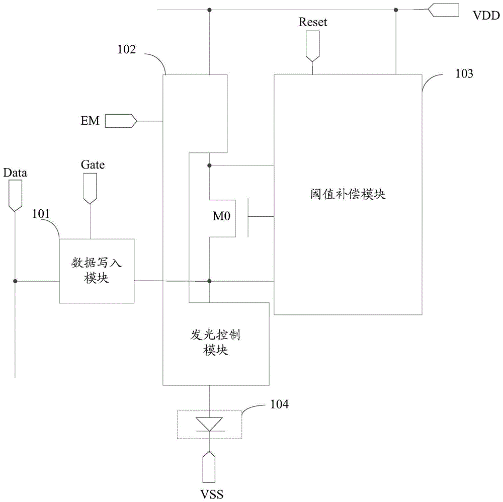
本发明实施例提供了一种像素电路,如图1所示,包括驱动晶体管M0、数据写入模块101、发光控制模块102、阈值补偿模块103和发光器件104;数据写入模块101被配置为响应于扫描信号端Gate的信号,将数据信号端Data的信号提供给驱动晶体管的第二极;阈值补偿模块103被配置为响应于复位信号端Reset的信号,对驱动晶体管M0的栅极进行复位,以及对驱动晶体管M0的阈值电压进行补偿;发光控制模块102被配置为响应于发光控制端EM的信号,将第一电压端VDD的信号提供给驱动晶体管M0的第一极,并将驱动晶体管M0的第二极与发光器件104导通;驱动晶体管M0被配置为根据驱动晶体管M0的栅极电压和第二极电压生成驱动电流,以通过驱动电流驱动发光器件104发光。An embodiment of the present invention provides a pixel circuit, as shown in FIG. 1 , including a driving transistor M0, a
本发明实施例提供的像素电路,包括驱动晶体管、数据写入模块、发光控制模块、阈值补偿模块和发光器件;数据写入模块被配置为响应于扫描信号端的信号,将数据信号端的信号提供给驱动晶体管的第二极;阈值补偿模块被配置为响应于复位信号端的信号,对驱动晶体管的栅极进行复位,以及对驱动晶体管的阈值电压进行补偿;发光控制模块被配置为响应于发光控制端的信号,将第一电压端的信号提供给驱动晶体管的第一极,并将驱动晶体管的第二极与发光器件导通;驱动晶体管被配置为根据驱动晶体管的栅极电压和第二极电压生成驱动电流,以通过驱动电流驱动发光器件发光。因此,本发明实施例提供的像素电路,通过上述模块与元件的相互配合,可以对驱动晶体管的阈值电压进行补偿,使得驱动发光器件发光的驱动电流不受驱动模块的阈值电压影响,改善由于阈值电压不均匀导致的发光亮度不均的问题。并且,通过上述模块与元件的相互配合,可以对第一电压端的电压进行补偿,使得驱动电流不受第一电压端的电压影响,可以改善由于第一电压端的IRDrop导致的发光亮度不均的问题。The pixel circuit provided by the embodiment of the present invention includes a driving transistor, a data writing module, a light-emitting control module, a threshold compensation module, and a light-emitting device; the data writing module is configured to respond to the signal of the scanning signal terminal, and provide the signal of the data signal terminal to the the second pole of the driving transistor; the threshold compensation module is configured to reset the gate of the driving transistor and compensate the threshold voltage of the driving transistor in response to the signal of the reset signal terminal; the lighting control module is configured to respond to the signal of the lighting control terminal signal, the signal of the first voltage terminal is provided to the first pole of the driving transistor, and the second pole of the driving transistor is turned on with the light emitting device; the driving transistor is configured to generate a driving transistor according to the gate voltage and the second pole voltage of the driving transistor current to drive the light-emitting device to emit light through the driving current. Therefore, in the pixel circuit provided by the embodiment of the present invention, the threshold voltage of the driving transistor can be compensated by the cooperation of the above-mentioned modules and components, so that the driving current for driving the light-emitting device to emit light is not affected by the threshold voltage of the driving module, and the threshold voltage due to the threshold voltage is improved. The problem of uneven luminous brightness caused by uneven voltage. In addition, through the cooperation of the above modules and components, the voltage of the first voltage terminal can be compensated, so that the driving current is not affected by the voltage of the first voltage terminal, and the problem of uneven brightness caused by the IRDrop of the first voltage terminal can be improved.
下面结合具体实施例,对本发明进行详细说明。需要说明的是,本实施例中是为了更好的解释本发明,但不限制本发明。The present invention will be described in detail below with reference to specific embodiments. It should be noted that this embodiment is for better explanation of the present invention, but does not limit the present invention.
实施例一、Embodiment 1.
在具体实施时,在本发明实施例提供的像素电路中,如图2所示,阈值补偿模块103包括第一子模块1031,第二子模块1032和第三子模块1033;第一子模块1031被配置为存储驱动晶体M0的栅极G与驱动晶体管M0第二极D的电压;第二子模块1032被配置为响应于复位信号端Reset的信号,将驱动晶体管M0的第一极S与驱动晶体管的栅极G导通;第三子模块1033被配置为存储第一电压端VDD与驱动晶体管M0的栅极G的电压。During specific implementation, in the pixel circuit provided by the embodiment of the present invention, as shown in FIG. 2 , the
在具体实施时,在本发明实施例提供的像素电路中,如图3所示,第一子模块1031包括第一电容C1,第一电容C1的第一端与驱动晶体管M0的第二极D耦接,第一电容C1的第二端与驱动晶体管M0栅极G耦接。During specific implementation, in the pixel circuit provided by the embodiment of the present invention, as shown in FIG. 3 , the first sub-module 1031 includes a first capacitor C1, the first end of the first capacitor C1 and the second electrode D of the driving transistor M0 The second end of the first capacitor C1 is coupled to the gate G of the driving transistor M0.
在具体实施时,在本发明实施例提供的像素电路中,如图3所示,第二子模块1032包括第一晶体管M1,第一晶体管M1的栅极与复位信号端Reset耦接,第一晶体管M1的第一极与驱动晶体管M0的第一极S耦接,第一晶体管M1的第二极与驱动晶体管M0的栅极G耦接。During specific implementation, in the pixel circuit provided by the embodiment of the present invention, as shown in FIG. 3 , the second sub-module 1032 includes a first transistor M1, the gate of the first transistor M1 is coupled to the reset signal terminal Reset, and the first transistor M1 The first electrode of the transistor M1 is coupled to the first electrode S of the driving transistor M0, and the second electrode of the first transistor M1 is coupled to the gate G of the driving transistor M0.
在具体实施时,在本发明实施例提供的像素电路中,如图3所示,第三子模块1033包括:第二电容C2,第二电容C2的一端与第一电压端VDD耦接,第二电容C2的第二端与驱动晶体管M0的栅极G耦接。During specific implementation, in the pixel circuit provided by the embodiment of the present invention, as shown in FIG. 3 , the third sub-module 1033 includes: a second capacitor C2, one end of the second capacitor C2 is coupled to the first voltage terminal VDD, and the first The second terminal of the two capacitors C2 is coupled to the gate G of the driving transistor M0.
在具体实施时,在本发明实施例提供的像素电路中,如图3所示,数据写入模块101包括第二晶体管M2,第二晶体管M2的栅极与扫描信号端Gate耦接,第二晶体管M2的第一极与数据信号端Data耦接,第二晶体管M2的第二极与驱动晶体管M0的第二极D耦接。During specific implementation, in the pixel circuit provided by the embodiment of the present invention, as shown in FIG. 3 , the
在具体实施时,在本发明实施例提供的像素电路中,如图3所示,发光控制模块102包括第三晶体管M3和第四晶体管M4;第三晶体管M3的栅极与发光控制端EM耦接,第三晶体管M3的第一极与驱动晶体管M0的第二极D耦接,第三晶体管M3的第二极与发光器件104的第一极耦接;第四晶体管M4的栅极与发光控制EM端耦接,第四晶体管M4的第一极与第一电压端VDD耦接,第四晶体管M4的第二极与驱动晶体管M0的第一极S耦接。During specific implementation, in the pixel circuit provided by the embodiment of the present invention, as shown in FIG. 3 , the light-emitting
在具体实施时,在本发明实施例提供的像素电路中,如图2所示,发光器件104的第一端与发光控制模块102耦接,发光器件104的第二端与第二电压端VSS耦接。并且,在具体实施时,发光器件104可以为:有机发光二极管(Organic Light Emitting Diode,OLED)、量子点发光二极管(Quantum Dot Light Emitting Diodes,QLED)中的至少一种。例如,发光器件104为OLED时,OLED的正极为发光器件104的第一端,负极为发光器件104的第二端。During specific implementation, in the pixel circuit provided by the embodiment of the present invention, as shown in FIG. 2 , the first end of the
一般在发光器件两端的电压差大于其开启电压的开启电压值时,发光器件可以发光。在具体实施时,在本发明实施例提供的像素电路中,如图3所示,数据信号端Data的电压值Vdata、第二电压端VSS的电压值Vss以及发光器件104的开启电压值Voled满足关系式:2Voled+Vss>Vdata>Voled+Vss。Generally, when the voltage difference across the light-emitting device is greater than the turn-on voltage value of the turn-on voltage, the light-emitting device can emit light. In specific implementation, in the pixel circuit provided by the embodiment of the present invention, as shown in FIG. 3 , the voltage value Vdata of the data signal terminal Data, the voltage value Vss of the second voltage terminal VSS, and the turn-on voltage value Voled of the
在具体实施时,在本发明实施例提供的像素电路中,上述各晶体管均是以P型晶体管为例示出的,对于上述晶体管为N型晶体管的情况,设计原理与本发明相同,也属于本发明保护的范围。During specific implementation, in the pixel circuit provided by the embodiment of the present invention, the above transistors are all shown by taking P-type transistors as an example. For the case where the above-mentioned transistors are N-type transistors, the design principle is the same as that of the present invention, which also belongs to the present invention. Scope of invention protection.
以上仅是举例说明本发明实施例提供的像素电路中各电路的具体结构,在具体实施时,上述各电路的具体结构不限于本发明实施例提供的上述结构,还可以是本领域技术人员可知的其他结构,在此不作限定。The above is only an example to illustrate the specific structure of each circuit in the pixel circuit provided by the embodiment of the present invention. During specific implementation, the specific structure of each of the above circuits is not limited to the above-mentioned structure provided by the embodiment of the present invention, and may also be known to those skilled in the art. Other structures are not limited here.
具体地,在本发明实施例提供的像素电路中,上述各晶体管可以是薄膜晶体管(TFT,Thin Film Transistor),也可以是金属氧化物半导体场效应管(MOS,Metal OxideScmiconductor),在此不作限定。并且根据上述各晶体管的类型以及各晶体管的栅极的信号的不同,可以将上述晶体管的第一极作为源极,第二极作为漏极,或者将晶体管的第一极作为漏极,第二极作为源极,在此不作具体区分。Specifically, in the pixel circuit provided by the embodiment of the present invention, the above-mentioned transistors may be thin film transistors (TFT, Thin Film Transistor) or metal oxide semiconductor field effect transistors (MOS, Metal Oxide Scmiconductor), which is not limited here. . And according to the type of each transistor and the signal of the gate of each transistor, the first electrode of the transistor can be used as the source electrode and the second electrode as the drain electrode, or the first electrode of the transistor can be used as the drain electrode and the second electrode as the drain electrode. The pole is used as the source, and no specific distinction is made here.
下面结合电路时序图对本发明实施例提供的像素电路的工作过程作以描述。下述描述中以1表示高电平,0表示低电平。需要说明的是,1和0是逻辑电平,其仅是为了更好的解释本发明实施例的具体工作过程,而不是具体的电压值。The working process of the pixel circuit provided by the embodiment of the present invention is described below with reference to the circuit timing diagram. In the following description, 1 means high level and 0 means low level. It should be noted that, 1 and 0 are logic levels, which are only to better explain the specific working process of the embodiment of the present invention, rather than specific voltage values.
以图3所示的像素电路为例,对应输入信号的时序图如图4所示。图4中所示的信号时序图包括:初始化阶段T1、阈值补偿阶段T2、数据写入阶段T3、发光阶段T4。其中,第一电压端VDD的信号的电压为Vdd,第二电压端VSS的信号的电压为Vss。Taking the pixel circuit shown in FIG. 3 as an example, the timing diagram corresponding to the input signal is shown in FIG. 4 . The signal timing diagram shown in FIG. 4 includes an initialization phase T1, a threshold compensation phase T2, a data writing phase T3, and a light-emitting phase T4. The voltage of the signal at the first voltage terminal VDD is Vdd, and the voltage of the signal at the second voltage terminal VSS is Vss.
在初始化阶段T1,EM=1,Gate=1,Reset=1;In the initialization phase T1, EM=1, Gate=1, Reset=1;
由于Gate=1,第二晶体管M2导通,将数据信号端Data的信号的电压Vref提供给驱动晶体管M0的第二极D。由于EM=1,第三晶体管M3、第四晶体管M4导通,导通的第四晶体管M4将第一电压端VDD的信号提供给驱动晶体管M0的第一极S,驱动晶体管M0的第一极S的电压为Vdd。导通的第三晶体管M3将驱动晶体管M0的第二极D的信号提供给发光器件104的第一极,发光器件104第一极被初始化。由于Reset=1,第一晶体管M1导通,将驱动晶体管M0的第一极S的电压Vdd提供给驱动晶体管M0的栅极G,驱动晶体管M0的栅极G的信号的电压为Vdd。第一电容C1存储驱动晶体管M0的栅极G与驱动晶体管M0的第二极D的电压;第二电容C2存储第一电压端VDD与驱动晶体管M0的栅极G的电压。Since Gate=1, the second transistor M2 is turned on, and the voltage Vref of the signal of the data signal terminal Data is supplied to the second electrode D of the driving transistor M0. Since EM=1, the third transistor M3 and the fourth transistor M4 are turned on, and the turned-on fourth transistor M4 provides the signal of the first voltage terminal VDD to the first pole S of the driving transistor M0, and the first pole of the driving transistor M0 The voltage of S is Vdd. The turned-on third transistor M3 provides the signal of the second electrode D of the driving transistor M0 to the first electrode of the
阈值补偿阶段T2,EM=0,Gate=1,Reset=1;Threshold compensation stage T2, EM=0, Gate=1, Reset=1;
由于EM=0,第三晶体管M3和第四晶体管M4截止。由于Gate=1,第二晶体管M2导通,将数据信号端Data的信号的电压Vdata提供给驱动晶体管M0的第二极D,驱动晶体管M0的第二极D的电压由Vref变为Vdata。由于Reset=1,第一晶体管M1导通,驱动晶体管M0第一极S与栅极G导通,使驱动晶体管M0形成二极管结构,驱动晶体管M0的栅极电压放电,在驱动晶体管M0的栅极电压变化为Vdata+Vth时,驱动晶体管M0截止。其中Vth为驱动晶体管M0的阈值电压。第一电容C1存储驱动晶体管M0的栅极G与驱动晶体管M0第二极D的电压,第二电容C2存储第一电压端VDD与驱动晶体管M0的栅极G的电压。Since EM=0, the third transistor M3 and the fourth transistor M4 are turned off. Since Gate=1, the second transistor M2 is turned on, and the voltage Vdata of the signal of the data signal terminal Data is provided to the second electrode D of the driving transistor M0, and the voltage of the second electrode D of the driving transistor M0 changes from Vref to Vdata. Since Reset=1, the first transistor M1 is turned on, the first electrode S and the gate G of the driving transistor M0 are turned on, so that the driving transistor M0 forms a diode structure, the gate voltage of the driving transistor M0 is discharged, and the gate of the driving transistor M0 is discharged. When the voltage changes to Vdata+Vth, the driving transistor M0 is turned off. Wherein Vth is the threshold voltage of the driving transistor M0. The first capacitor C1 stores the voltage of the gate G of the driving transistor M0 and the second electrode D of the driving transistor M0, and the second capacitor C2 stores the voltage of the first voltage terminal VDD and the gate G of the driving transistor M0.
数据写入阶段T3,EM=0,Gate=1,Reset=0;Data writing stage T3, EM=0, Gate=1, Reset=0;
由于EM=0,第三晶体管M3和第四晶体管M4截止。由于Reset=0,第一晶体管M1截止。由于Gate=1,第二晶体管M2导通,将数据信号端Data的信号的电压Vref提供给驱动晶体管M0的第二极D,驱动晶体管M0的第二极D的电压由Vdata变为Vref,则驱动晶体管M0的栅极G的信号由Vdata+Vth变为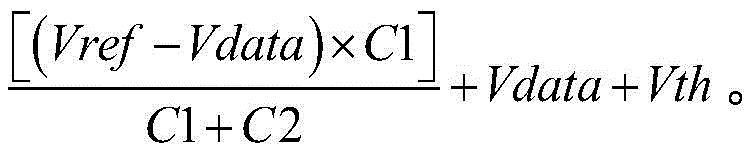
发光阶段T4,EM=1,EM=0,Gate=0,Reset=0;Light-emitting stage T4, EM=1, EM=0, Gate=0, Reset=0;
由于Reset=0,第一晶体管M1截止。由于Gate=0,第二晶体管M2截止。由于EM=1,第三晶体管M3和第四晶体管M4导通。驱动晶体管M0的第二极D的电压由Vref变为Voled+Vss。导通的第四晶体管M4将第一电压端VDD的信号提供给驱动晶体管M0的第一极S,导通的第三晶体管M3将驱动晶体管M0的第二极D与发光器件104导通。驱动晶体管M0的栅极G的信号的电压值VG变化为:Since Reset=0, the first transistor M1 is turned off. Since Gate=0, the second transistor M2 is turned off. Since EM=1, the third transistor M3 and the fourth transistor M4 are turned on. The voltage of the second electrode D of the driving transistor M0 changes from Vref to Voled+Vss. The turned-on fourth transistor M4 provides the signal of the first voltage terminal VDD to the first pole S of the driving transistor M0, and the turned-on third transistor M3 turns on the second pole D of the driving transistor M0 and the

故此可以得到驱动晶体管M0的栅极G与第二极D之间的电压差VGD为:Therefore, the voltage difference V GD between the gate G and the second electrode D of the driving transistor M0 can be obtained as:

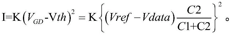
驱动晶体管M0驱动发光器件发光的驱动电流I为:The driving current I of the driving transistor M0 for driving the light-emitting device to emit light is:

从上述公式可以得知,此时驱动晶体管M0的输出的驱动电流I已经不受驱动晶体管M0的阈值电压Vth与第一电压源VDD的压降的影响,因此改善了驱动晶体管M0由于工艺制程及长时间的操作造成阈值电压漂移以及第一电压源VDD的压降的问题,从而提高显示效果。It can be known from the above formula that the driving current I output by the driving transistor M0 is not affected by the threshold voltage Vth of the driving transistor M0 and the voltage drop of the first voltage source VDD, thus improving the driving transistor M0 due to the process and The long-term operation causes problems of threshold voltage drift and voltage drop of the first voltage source VDD, thereby improving the display effect.
并且,从上述公式可以得知,数据信号端Data仅需提供合适的电压Vdata,即可以使驱动电流I不受发光器件104的开启电压值Voled的影响。进而当发光器件104老化,导致其开启电压值发生变化时,可以通过调整数据电压端Data的电压Vdata,使得驱动晶体管M0驱动发光器件104发光的驱动电流不受发光器件老化程度的影响。Furthermore, it can be known from the above formula that the data signal terminal Data only needs to provide an appropriate voltage Vdata, that is, the driving current I can be not affected by the turn-on voltage value Voled of the
实施例二、Embodiment two,
本发明实施例对应的像素电路的结构示意图如图5所示,其针对实施例一中的实施方式进行了变形。下面仅说明本实施例与实施例一的区别之处,其相同之处在此不作赘述。A schematic structural diagram of a pixel circuit corresponding to an embodiment of the present invention is shown in FIG. 5 , which is modified from the implementation in the first embodiment. Only the differences between this embodiment and the first embodiment will be described below, and the similarities will not be repeated here.
在具体实施时,在本发明实施例提供的像素电路中,阈值补偿模块103还包括第四子模块,其中,驱动晶体管的栅极通过第四子模块与第二电容的第二端耦接;第四子模块被配置为响应于扫描信号端的信号,将驱动晶体管的栅极与第二电容的第二端导通。During specific implementation, in the pixel circuit provided by the embodiment of the present invention, the
在具体实施时,在本发明实施例提供的像素电路中,第四子模块包括第五晶体管M5,第五晶体管M5的栅极与扫描信号端Gate耦接,第五晶体管M5的第一极与第二电容C2的第二端耦接,第五晶体管M5的第二极与驱动晶体管M0的栅极耦接。During specific implementation, in the pixel circuit provided by the embodiment of the present invention, the fourth sub-module includes a fifth transistor M5, the gate of the fifth transistor M5 is coupled to the scanning signal terminal Gate, and the first pole of the fifth transistor M5 is connected to the scanning signal terminal Gate. The second terminal of the second capacitor C2 is coupled, and the second electrode of the fifth transistor M5 is coupled to the gate of the driving transistor M0.
下面结合电路时序图对本发明实施例提供的像素电路的工作过程作以描述。下述描述中以1表示高电平,0表示低电平。需要说明的是,1和0是逻辑电平,其仅是为了更好的解释本发明实施例的具体工作过程,而不是具体的电压值。The working process of the pixel circuit provided by the embodiment of the present invention is described below with reference to the circuit timing diagram. In the following description, 1 means high level and 0 means low level. It should be noted that, 1 and 0 are logic levels, which are only to better explain the specific working process of the embodiment of the present invention, rather than specific voltage values.
以图5所示的像素电路为例,对应输入信号的时序图如图6所示。图6中所示的信号时序图包括:初始化阶段T1、阈值补偿阶段T2、数据写入阶段T3、缓冲阶段T3’,发光阶段T4。其中,第一电压端VDD的信号的电压为Vdd,第二电压端VSS的信号的电压为Vss。Taking the pixel circuit shown in FIG. 5 as an example, the timing diagram corresponding to the input signal is shown in FIG. 6 . The signal timing diagram shown in FIG. 6 includes an initialization phase T1, a threshold compensation phase T2, a data writing phase T3, a buffer phase T3', and a light-emitting phase T4. The voltage of the signal at the first voltage terminal VDD is Vdd, and the voltage of the signal at the second voltage terminal VSS is Vss.
在初始化阶段T1,EM=1,Gate=1,Reset=1;In the initialization phase T1, EM=1, Gate=1, Reset=1;
由于Gate=1,第二晶体管M2和第五晶体管M5导通。导通的第二晶体管M2将数据信号端Data的信号的电压Vref提供给驱动晶体管M0的第二极D。第五晶体管M5将第二电容C2第二端与驱动晶体管M0的栅极导通。由于EM=1,第三晶体管M3、第四晶体管M4导通,导通的第四晶体管M4将第一电压端VDD的信号提供给驱动晶体管M0的第一极S,驱动晶体管M0的第一极S的电压为Vdd。导通的第三晶体管M3将驱动晶体管M0的第二极D的信号提供给发光器件104的第一极,发光器件104第一极被初始化。由于Reset=1,第一晶体管M1导通,将驱动晶体管M0的第一极S的电压Vdd提供给驱动晶体管M0的栅极G,驱动晶体管M0的栅极G的信号的电压为Vdd。第一电容C1存储驱动晶体管M0的栅极G与驱动晶体管M0的第二极D的电压;第二电容C2存储第一电压端VDD与驱动晶体管M0的栅极G的电压。Since Gate=1, the second transistor M2 and the fifth transistor M5 are turned on. The turned-on second transistor M2 supplies the voltage Vref of the signal of the data signal terminal Data to the second electrode D of the driving transistor M0. The fifth transistor M5 conducts the second end of the second capacitor C2 with the gate of the driving transistor M0. Since EM=1, the third transistor M3 and the fourth transistor M4 are turned on, and the turned-on fourth transistor M4 provides the signal of the first voltage terminal VDD to the first pole S of the driving transistor M0, and the first pole of the driving transistor M0 The voltage of S is Vdd. The turned-on third transistor M3 provides the signal of the second electrode D of the driving transistor M0 to the first electrode of the
阈值补偿阶段T2,EM=0,Gate=1,Reset=1;Threshold compensation stage T2, EM=0, Gate=1, Reset=1;
由于EM=0,第三晶体管M3和第四晶体管M4截止。由于Gate=1,第二晶体管M2和第五晶体管M5导通,导通的第二晶体管M2将数据信号端Data的信号的电压Vref提供给驱动晶体管M0的第二极D。导通的第五晶体管M5将第二电容C2第二端与驱动晶体管M0的栅极G导通。由于Reset=1,第一晶体管M1导通,驱动晶体管M0第一极S与栅极G导通,使驱动晶体管M0形成二极管结构,驱动晶体管M0的栅极电压放电,在驱动晶体管M0的栅极电压由Vdd变化为Vref+Vth时,驱动晶体管M0截止,并且Vdd-Vref>Vth。其中Vth为驱动晶体管M0的阈值电压。第一电容C1存储驱动晶体管M0的栅极G与驱动晶体管M0第二极D的电压,第二电容C2存储第一电压端VDD与驱动晶体管M0的栅极G的电压。Since EM=0, the third transistor M3 and the fourth transistor M4 are turned off. Since Gate=1, the second transistor M2 and the fifth transistor M5 are turned on, and the turned-on second transistor M2 provides the voltage Vref of the signal of the data signal terminal Data to the second electrode D of the driving transistor M0. The turned-on fifth transistor M5 turns on the second end of the second capacitor C2 and the gate G of the driving transistor M0. Since Reset=1, the first transistor M1 is turned on, the first electrode S and the gate G of the driving transistor M0 are turned on, so that the driving transistor M0 forms a diode structure, the gate voltage of the driving transistor M0 is discharged, and the gate of the driving transistor M0 is discharged. When the voltage changes from Vdd to Vref+Vth, the driving transistor M0 is turned off, and Vdd-Vref>Vth. Wherein Vth is the threshold voltage of the driving transistor M0. The first capacitor C1 stores the voltage of the gate G of the driving transistor M0 and the second electrode D of the driving transistor M0, and the second capacitor C2 stores the voltage of the first voltage terminal VDD and the gate G of the driving transistor M0.
数据写入阶段T3,EM=0,Gate=1,Reset=0;Data writing stage T3, EM=0, Gate=1, Reset=0;
由于EM=0,第三晶体管M3和第四晶体管M4截止。由于Reset=0,第一晶体管M1截止。由于Gate=1,第二晶体管M2和第五晶体管M5导通,将数据信号端Data的信号的电压Vdata提供给驱动晶体管M0的第二极D,驱动晶体管M0的第二极D的电压由Vref变为Vdata,则驱动晶体管M0的栅极G的信号由Vref+Vth变为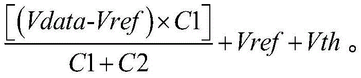

缓冲阶段T3’,EM=0,Gate=0,Reset=0;Buffer stage T3', EM=0, Gate=0, Reset=0;
由于EM=0,第三晶体管M3和第四晶体管M4截止。由于Gate=0,第二晶体管M2和第五晶体管M5截止。由于Reset=0,第一晶体管M1截止。此时第一电容C1两端的电压与数据写入阶段T3的驱动晶体管M0的栅极G与第二极D的电压相同,即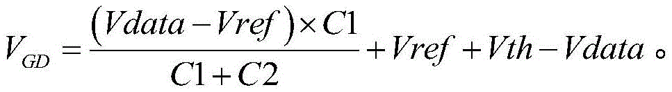
发光阶段T4,EM=1,EM=0,Gate=0,Reset=0;Light-emitting stage T4, EM=1, EM=0, Gate=0, Reset=0;
由于Reset=0,第一晶体管M1截止。由于Gate=0,第二晶体管M2和第五晶体管M5截止。由于EM=1,第三晶体管M3和第四晶体管M4导通。驱动晶体管M0的第二极D的电压由Vdata变为Voled+Vss。导通的第四晶体管M4将第一电压端VDD的信号提供给驱动晶体管M0的第一极S,导通的第三晶体管M3将驱动晶体管M0的第二极D与发光器件104导通。驱动晶体管M0的栅极G与第二极D之间的电压差VGD为:Since Reset=0, the first transistor M1 is turned off. Since Gate=0, the second transistor M2 and the fifth transistor M5 are turned off. Since EM=1, the third transistor M3 and the fourth transistor M4 are turned on. The voltage of the second electrode D of the driving transistor M0 changes from Vdata to Voled+Vss. The turned-on fourth transistor M4 provides the signal of the first voltage terminal VDD to the first pole S of the driving transistor M0, and the turned-on third transistor M3 turns on the second pole D of the driving transistor M0 and the

驱动晶体管M0驱动发光器件发光的驱动电流I为:The driving current I of the driving transistor M0 for driving the light-emitting device to emit light is:

从上述公式可以得知,此时驱动晶体管M0的输出的驱动电流I已经不受驱动晶体管M0的阈值电压Vth与第一电压源VDD的压降的影响,因此改善了驱动晶体管M0由于工艺制程及长时间的操作造成阈值电压漂移以及第一电压源VDD的压降的问题,从而提高显示效果。It can be known from the above formula that the driving current I output by the driving transistor M0 is not affected by the threshold voltage Vth of the driving transistor M0 and the voltage drop of the first voltage source VDD, thus improving the driving transistor M0 due to the process and The long-term operation causes problems of threshold voltage drift and voltage drop of the first voltage source VDD, thereby improving the display effect.
基于同一发明构思,本发明实施例还提供了一种本发明实施例提供的像素电路的驱动方法,如图7所示,该方法包括步骤701-步骤704;Based on the same inventive concept, an embodiment of the present invention also provides a method for driving a pixel circuit provided by an embodiment of the present invention. As shown in FIG. 7 , the method includes
步骤701,初始化阶段,数据写入模块响应于扫描信号端的信号,将数据信号端的信号提供给驱动晶体管的第二极;阈值补偿模块响应于复位信号端的信号,对驱动晶体管的栅极进行复位;发光控制模块响应于发光控制端的信号,将第一电压端的信号提供给驱动晶体管的第一极,并将驱动晶体管的第二极与发光器件导通;
步骤702,阈值补偿阶段,数据写入模块响应于扫描信号端的信号,将数据信号端的信号提供给驱动晶体管的第二极;阈值补偿模块对驱动晶体管的阈值电压进行补偿;
步骤703,数据写入阶段,数据写入模块响应于扫描信号端的信号,将数据信号端的信号提供给驱动晶体管的第二极;
步骤704,发光阶段,发光控制模块响应于发光控制端的信号,将第一电压端的信号提供给驱动晶体管的第一极,并将驱动晶体管的第二极与发光器件导通;驱动晶体管根据驱动晶体管的栅极电压和第二极电压生成驱动电流,以通过驱动电流驱动发光器件发光。
基于同一发明构思,本发明实施例还提供了一种显示装置,包括本发明实施例提供的上述像素电路。该显示装置的实施可以参见上述像素电路的实施例,重复之处不再赘述。Based on the same inventive concept, an embodiment of the present invention further provides a display device, including the above-mentioned pixel circuit provided by the embodiment of the present invention. For the implementation of the display device, reference may be made to the above-mentioned embodiments of the pixel circuit, and repeated descriptions will not be repeated.
在具体实施时,本发明实施例提供的上述显示装置可以为如图8所示的全面屏的手机。当然,本发明实施例提供的上述显示装置也可以为:手机、平板电脑、电视机、显示器、笔记本电脑、数码相框、导航仪等任何具有显示功能的产品或部件。对于该显示装置的其它必不可少的组成部分均为本领域的普通技术人员应该理解具有的,在此不做赘述,也不应作为对本发明的限制。During specific implementation, the above-mentioned display device provided by the embodiment of the present invention may be a mobile phone with a full screen as shown in FIG. 8 . Of course, the above-mentioned display device provided in the embodiment of the present invention may also be any product or component with display function, such as a mobile phone, a tablet computer, a television, a monitor, a notebook computer, a digital photo frame, and a navigator. Other essential components of the display device should be understood by those of ordinary skill in the art, and will not be repeated here, nor should it be regarded as a limitation of the present invention.
本发明实施例提供的像素电路、其驱动方法及显示装置,包括驱动晶体管、数据写入模块、发光控制模块、阈值补偿模块和发光器件;数据写入模块被配置为响应于扫描信号端的信号,将数据信号端的信号提供给驱动晶体管的第二极;阈值补偿模块被配置为响应于复位信号端的信号,对驱动晶体管的栅极进行复位,以及对驱动晶体管的阈值电压进行补偿;发光控制模块被配置为响应于发光控制端的信号,将第一电压端的信号提供给驱动晶体管的第一极,并将驱动晶体管的第二极与发光器件导通;驱动晶体管被配置为根据驱动晶体管的栅极电压和第二极电压生成驱动电流,以通过驱动电流驱动发光器件发光。因此,本发明实施例提供的像素电路,通过上述模块与元件的相互配合,可以对驱动晶体管的阈值电压进行补偿,使得驱动发光器件发光的驱动电流不受驱动模块的阈值电压影响,改善由于阈值电压不均匀导致的发光亮度不均的问题。并且,通过上述模块与元件的相互配合,可以对第一电压端的电压进行补偿,使得驱动电流不受第一电压端的电压影响,可以改善由于第一电压端的IR Drop导致的发光亮度不均的问题。The pixel circuit, the driving method thereof, and the display device provided by the embodiments of the present invention include a driving transistor, a data writing module, a light-emitting control module, a threshold compensation module, and a light-emitting device; the data writing module is configured to respond to the signal of the scanning signal terminal, The signal of the data signal terminal is provided to the second pole of the driving transistor; the threshold value compensation module is configured to reset the gate of the driving transistor and compensate the threshold voltage of the driving transistor in response to the signal of the reset signal terminal; is configured to provide the signal of the first voltage terminal to the first electrode of the driving transistor in response to the signal of the light-emitting control terminal, and conduct the second electrode of the driving transistor with the light-emitting device; the driving transistor is configured to be based on the gate voltage of the driving transistor and the second electrode voltage to generate a driving current to drive the light emitting device to emit light through the driving current. Therefore, in the pixel circuit provided by the embodiment of the present invention, the threshold voltage of the driving transistor can be compensated by the cooperation of the above-mentioned modules and components, so that the driving current for driving the light-emitting device to emit light is not affected by the threshold voltage of the driving module, and the threshold voltage due to the threshold voltage is improved. The problem of uneven luminous brightness caused by uneven voltage. In addition, through the cooperation of the above-mentioned modules and components, the voltage of the first voltage terminal can be compensated, so that the driving current is not affected by the voltage of the first voltage terminal, and the problem of uneven luminous brightness caused by the IR Drop of the first voltage terminal can be improved. .
Claims (5)
Priority Applications (1)
| Application Number | Priority Date | Filing Date | Title |
|---|---|---|---|
| CN201910852504.9A CN110544458B (en) | 2019-09-10 | 2019-09-10 | A pixel circuit, a driving method thereof, and a display device |
Applications Claiming Priority (1)
| Application Number | Priority Date | Filing Date | Title |
|---|---|---|---|
| CN201910852504.9A CN110544458B (en) | 2019-09-10 | 2019-09-10 | A pixel circuit, a driving method thereof, and a display device |
Publications (2)
| Publication Number | Publication Date |
|---|---|
| CN110544458A CN110544458A (en) | 2019-12-06 |
| CN110544458B true CN110544458B (en) | 2021-08-06 |
Family
ID=68713186
Family Applications (1)
| Application Number | Title | Priority Date | Filing Date |
|---|---|---|---|
| CN201910852504.9A Active CN110544458B (en) | 2019-09-10 | 2019-09-10 | A pixel circuit, a driving method thereof, and a display device |
Country Status (1)
| Country | Link |
|---|---|
| CN (1) | CN110544458B (en) |
Families Citing this family (6)
| Publication number | Priority date | Publication date | Assignee | Title |
|---|---|---|---|---|
| KR102811546B1 (en) * | 2019-12-30 | 2025-05-21 | 엘지디스플레이 주식회사 | Pixel circuit and light emitting display device and driving method for the same |
| CN111508423B (en) * | 2020-04-28 | 2023-01-24 | 昆山国显光电有限公司 | Pixel driving circuit, array substrate, display panel and display device |
| CN113870793A (en) * | 2021-09-29 | 2021-12-31 | 北京京东方技术开发有限公司 | Pixel circuit, driving method thereof, display substrate and display device |
| US20240265866A1 (en) * | 2022-04-24 | 2024-08-08 | Chongqing Boe Display Technology Co., Ltd. | Pixel circuit and drive method therefor, display panel and display device |
| CN114822407A (en) * | 2022-05-27 | 2022-07-29 | 云谷(固安)科技有限公司 | Pixel driving circuit, driving method of pixel driving circuit and display panel |
| CN116844481A (en) * | 2023-07-31 | 2023-10-03 | 云谷(固安)科技有限公司 | Pixel circuit, driving method and display device |
Family Cites Families (9)
| Publication number | Priority date | Publication date | Assignee | Title |
|---|---|---|---|---|
| JP4195337B2 (en) * | 2002-06-11 | 2008-12-10 | 三星エスディアイ株式会社 | Light emitting display device, display panel and driving method thereof |
| JP4484451B2 (en) * | 2003-05-16 | 2010-06-16 | 奇美電子股▲ふん▼有限公司 | Image display device |
| CN104025176A (en) * | 2011-11-24 | 2014-09-03 | 松下电器产业株式会社 | Display device and control method thereof |
| JP2015025978A (en) * | 2013-07-26 | 2015-02-05 | 株式会社ジャパンディスプレイ | Drive circuit, display device, and drive method |
| CN105590581A (en) * | 2014-10-21 | 2016-05-18 | 张学一 | Current type pixel driving circuit of organic light-emitting diode |
| KR20170074620A (en) * | 2015-12-22 | 2017-06-30 | 엘지디스플레이 주식회사 | Sub-pixel of organic light emitting display device and organic light emitting display device including the same |
| KR20170074618A (en) * | 2015-12-22 | 2017-06-30 | 엘지디스플레이 주식회사 | Sub-pixel of organic light emitting display device and organic light emitting display device including the same |
| CN107516488A (en) * | 2017-09-20 | 2017-12-26 | 上海天马有机发光显示技术有限公司 | A kind of image element circuit, its driving method, display panel and display device |
| CN109754757B (en) * | 2019-03-28 | 2020-11-06 | 京东方科技集团股份有限公司 | Pixel driving circuit, display device and pixel driving method |
-
2019
- 2019-09-10 CN CN201910852504.9A patent/CN110544458B/en active Active
Also Published As
| Publication number | Publication date |
|---|---|
| CN110544458A (en) | 2019-12-06 |
Similar Documents
| Publication | Publication Date | Title |
|---|---|---|
| CN110544458B (en) | A pixel circuit, a driving method thereof, and a display device | |
| US10497323B2 (en) | Pixel circuit, method for driving the same, display panel and display device | |
| CN108039149B (en) | OLED pixel circuit, driving method thereof and display device | |
| CN106652903B (en) | A kind of OLED pixel circuit and its driving method, display device | |
| CN104933993B (en) | Pixel-driving circuit and its driving method, display device | |
| WO2023005621A1 (en) | Pixel circuit and driving method therefor and display panel | |
| WO2023005648A1 (en) | Pixel circuit and driving method therefor, array substrate, and display device | |
| CN107230451B (en) | A kind of AMOLED pixel-driving circuits and image element driving method | |
| WO2019184266A1 (en) | Amoled pixel driving circuit, driving method, and terminal | |
| CN107369413B (en) | A pixel compensation circuit, a driving method thereof, a display panel and a display device | |
| CN110556076B (en) | Pixel circuit, driving method and display device | |
| CN105575327B (en) | A kind of image element circuit, its driving method and organic EL display panel | |
| CN107767819A (en) | Pixel-driving circuit and method, display device | |
| CN109979394A (en) | Pixel circuit and its driving method, array substrate and display device | |
| CN110136650A (en) | Pixel circuit, driving method thereof, array substrate and display device | |
| CN104537983B (en) | Image element circuit and its driving method, display device | |
| CN106486051B (en) | Pixel structure | |
| WO2020192278A1 (en) | Pixel circuit and driving method therefor, and display substrate and display device | |
| CN107369412B (en) | Pixel circuit, driving method thereof and display device | |
| WO2018219209A1 (en) | Pixel compensation circuit, compensation method, and display device | |
| CN105096826A (en) | Pixel circuit and driving method thereof, array substrate and display device | |
| CN109559686A (en) | Pixel circuit, driving method, electroluminescence display panel and display device | |
| WO2019174372A1 (en) | Pixel compensation circuit, drive method, electroluminescent display panel, and display device | |
| CN106067291A (en) | A kind of pixel-driving circuit and driving method, display device | |
| CN116631339A (en) | Pixel circuit, driving method thereof, display substrate and display device |
Legal Events
| Date | Code | Title | Description |
|---|---|---|---|
| PB01 | Publication | ||
| PB01 | Publication | ||
| SE01 | Entry into force of request for substantive examination | ||
| SE01 | Entry into force of request for substantive examination | ||
| GR01 | Patent grant | ||
| GR01 | Patent grant |