WO2011139055A2 - 유기광전자소자용 화합물, 이를 포함하는 유기발광소자 및 상기 유기발광소자를 포함하는 표시장치 - Google Patents
유기광전자소자용 화합물, 이를 포함하는 유기발광소자 및 상기 유기발광소자를 포함하는 표시장치 Download PDFInfo
- Publication number
- WO2011139055A2 WO2011139055A2 PCT/KR2011/003235 KR2011003235W WO2011139055A2 WO 2011139055 A2 WO2011139055 A2 WO 2011139055A2 KR 2011003235 W KR2011003235 W KR 2011003235W WO 2011139055 A2 WO2011139055 A2 WO 2011139055A2
- Authority
- WO
- WIPO (PCT)
- Prior art keywords
- group
- substituted
- unsubstituted
- formula
- compound
- Prior art date
- Legal status (The legal status is an assumption and is not a legal conclusion. Google has not performed a legal analysis and makes no representation as to the accuracy of the status listed.)
- Ceased
Links
- 0 C*1c2cc(-c(cc3)cc(*)c3-c3ccccc3I)ccc2-c2ccccc12 Chemical compound C*1c2cc(-c(cc3)cc(*)c3-c3ccccc3I)ccc2-c2ccccc12 0.000 description 2
- FRJBPOWMIQKYSK-UHFFFAOYSA-N c(cc1)ccc1-c(cc1)ccc1-[n]1c(ccc(-c(cc2)cc(c3c4cccc3)c2[n]4-c2nc(-c3ccccc3)cc(-c3ccccc3)n2)c2)c2c2ccccc12 Chemical compound c(cc1)ccc1-c(cc1)ccc1-[n]1c(ccc(-c(cc2)cc(c3c4cccc3)c2[n]4-c2nc(-c3ccccc3)cc(-c3ccccc3)n2)c2)c2c2ccccc12 FRJBPOWMIQKYSK-UHFFFAOYSA-N 0.000 description 2
- QXMKKEMEHVHGQX-UHFFFAOYSA-N c(cc1)ccc1-c(cc1)ccc1-[n]1c(ccc(-c(cc2)cc(c3c4cccc3)c2[n]4-c2nc(-c3ccccc3)nc(-c3ccccc3)n2)c2)c2c2ccccc12 Chemical compound c(cc1)ccc1-c(cc1)ccc1-[n]1c(ccc(-c(cc2)cc(c3c4cccc3)c2[n]4-c2nc(-c3ccccc3)nc(-c3ccccc3)n2)c2)c2c2ccccc12 QXMKKEMEHVHGQX-UHFFFAOYSA-N 0.000 description 2
- GPWPHOWXAKRMGN-JKTVRDLGSA-N N=C(/C=C(/c1ccccc1)\N[n](c(cccc1)c1c1c2)c1ccc2-c(cc1)cc(c2c3cccc2)c1[n]3-c1ccccc1)c1ccccc1 Chemical compound N=C(/C=C(/c1ccccc1)\N[n](c(cccc1)c1c1c2)c1ccc2-c(cc1)cc(c2c3cccc2)c1[n]3-c1ccccc1)c1ccccc1 GPWPHOWXAKRMGN-JKTVRDLGSA-N 0.000 description 1
- WYGUHDAPCNQTPR-CSVQLBLSSA-N N=C(/C=C(/c1ccccc1)\N[n](c(cccc1)c1c1c2)c1ccc2-c(cc1)cc(c2ccccc22)c1[n]2-c(cc1c2cc(-c3ccccc3)ccc22)ccc1[n]2-c1ccccc1)c1ccccc1 Chemical compound N=C(/C=C(/c1ccccc1)\N[n](c(cccc1)c1c1c2)c1ccc2-c(cc1)cc(c2ccccc22)c1[n]2-c(cc1c2cc(-c3ccccc3)ccc22)ccc1[n]2-c1ccccc1)c1ccccc1 WYGUHDAPCNQTPR-CSVQLBLSSA-N 0.000 description 1
- XYHJOSAZECEHLT-UHFFFAOYSA-N N=C(c1cc2c(cccc3)c3c(cccc3)c3c2cc1)/N=C(/c1ccc(c(cccc2)c2c2ccccc22)c2c1)\N[n](c(cccc1)c1c1c2)c1ccc2-c(cc1c2ccccc22)ccc1[n]2-c1ccccc1 Chemical compound N=C(c1cc2c(cccc3)c3c(cccc3)c3c2cc1)/N=C(/c1ccc(c(cccc2)c2c2ccccc22)c2c1)\N[n](c(cccc1)c1c1c2)c1ccc2-c(cc1c2ccccc22)ccc1[n]2-c1ccccc1 XYHJOSAZECEHLT-UHFFFAOYSA-N 0.000 description 1
- SPQSYUTYHBBUHT-UHFFFAOYSA-N [AlH2][n]1c(ccc(-c(cc2c3ccccc33)ccc2[n]3[IH][AlH2])c2)c2c2ccccc12 Chemical compound [AlH2][n]1c(ccc(-c(cc2c3ccccc33)ccc2[n]3[IH][AlH2])c2)c2c2ccccc12 SPQSYUTYHBBUHT-UHFFFAOYSA-N 0.000 description 1
- DQEWQQZXOPSDKY-UHFFFAOYSA-N c(cc1)ccc1-c(cc1)ccc1-[n]1c(ccc(-c(cc2c3c4cccc3)ccc2[n]4-c2nc(-c3ccccc3)cc(-c3ccccc3)c2)c2)c2c2ccccc12 Chemical compound c(cc1)ccc1-c(cc1)ccc1-[n]1c(ccc(-c(cc2c3c4cccc3)ccc2[n]4-c2nc(-c3ccccc3)cc(-c3ccccc3)c2)c2)c2c2ccccc12 DQEWQQZXOPSDKY-UHFFFAOYSA-N 0.000 description 1
- OXWIHTDISQQUFD-UHFFFAOYSA-N c(cc1)ccc1-c(cc1)ccc1-c1nc(-c(cc2)ccc2-c2ccccc2)nc(-[n](c(cccc2)c2c2c3)c2ccc3-c(cc2)cc(c3ccccc33)c2[n]3-c2ccccc2)n1 Chemical compound c(cc1)ccc1-c(cc1)ccc1-c1nc(-c(cc2)ccc2-c2ccccc2)nc(-[n](c(cccc2)c2c2c3)c2ccc3-c(cc2)cc(c3ccccc33)c2[n]3-c2ccccc2)n1 OXWIHTDISQQUFD-UHFFFAOYSA-N 0.000 description 1
- HXMYKRLVLPSOGR-UHFFFAOYSA-N c(cc1)ccc1-c(cc1c2cc(-[n]3c(ccc(-c(cc4c5c6cccc5)ccc4[n]6-c4nc(-c5ccccc5)cc(-c5ccccc5)c4)c4)c4c4ccccc34)ccc22)ccc1[n]2-c1ccccc1 Chemical compound c(cc1)ccc1-c(cc1c2cc(-[n]3c(ccc(-c(cc4c5c6cccc5)ccc4[n]6-c4nc(-c5ccccc5)cc(-c5ccccc5)c4)c4)c4c4ccccc34)ccc22)ccc1[n]2-c1ccccc1 HXMYKRLVLPSOGR-UHFFFAOYSA-N 0.000 description 1
- VJTWJTBTKAELQS-UHFFFAOYSA-N c(cc1)ccc1-c(cc1c2cc(-c(cc3)cc(c4c5ccc(-c6ccccc6)c4)c3[n]5-c3nc(-c4ccccc4)cc(-c4ccccc4)n3)ccc22)ccc1[n]2-c1ccccc1 Chemical compound c(cc1)ccc1-c(cc1c2cc(-c(cc3)cc(c4c5ccc(-c6ccccc6)c4)c3[n]5-c3nc(-c4ccccc4)cc(-c4ccccc4)n3)ccc22)ccc1[n]2-c1ccccc1 VJTWJTBTKAELQS-UHFFFAOYSA-N 0.000 description 1
- OHYFNWIMNCBDEK-UHFFFAOYSA-N c(cc1)ccc1-c(cc1c2cc(-c(cc3)cc(c4c5ccc(-c6ccccc6)c4)c3[n]5-c3nc(-c4ccccc4)nc(-c4ccccc4)n3)ccc22)ccc1[n]2-c1ccccc1 Chemical compound c(cc1)ccc1-c(cc1c2cc(-c(cc3)cc(c4c5ccc(-c6ccccc6)c4)c3[n]5-c3nc(-c4ccccc4)nc(-c4ccccc4)n3)ccc22)ccc1[n]2-c1ccccc1 OHYFNWIMNCBDEK-UHFFFAOYSA-N 0.000 description 1
- UTHXRTRPWRVYML-UHFFFAOYSA-N c(cc1)ccc1-c(cc1c2cc(-c(cc3c4c5ccc(-c6ccccc6)c4)ccc3[n]5-c3nc(-c4ccccc4)cc(-c4ccccc4)c3)ccc22)ccc1[n]2-c1ccccc1 Chemical compound c(cc1)ccc1-c(cc1c2cc(-c(cc3c4c5ccc(-c6ccccc6)c4)ccc3[n]5-c3nc(-c4ccccc4)cc(-c4ccccc4)c3)ccc22)ccc1[n]2-c1ccccc1 UTHXRTRPWRVYML-UHFFFAOYSA-N 0.000 description 1
- SULBQRWRGIQMGO-UHFFFAOYSA-N c(cc1)ccc1-c1cc(-[n](c(cccc2)c2c2c3)c2ccc3-c(cc2)cc(c3c4cccc3)c2[n]4-c2ccccc2)nc(-c2ccccc2)c1 Chemical compound c(cc1)ccc1-c1cc(-[n](c(cccc2)c2c2c3)c2ccc3-c(cc2)cc(c3c4cccc3)c2[n]4-c2ccccc2)nc(-c2ccccc2)c1 SULBQRWRGIQMGO-UHFFFAOYSA-N 0.000 description 1
- BZXHCAIVRTWMEK-UHFFFAOYSA-N c(cc1)ccc1-c1cc(-c(cc2)ccc2-[n](c(cccc2)c2c2c3)c2ccc3-c2cccc3c2[s]c2ccccc32)nc(-c2ccccc2)c1 Chemical compound c(cc1)ccc1-c1cc(-c(cc2)ccc2-[n](c(cccc2)c2c2c3)c2ccc3-c2cccc3c2[s]c2ccccc32)nc(-c2ccccc2)c1 BZXHCAIVRTWMEK-UHFFFAOYSA-N 0.000 description 1
- YRJOUUYCFRPLBC-UHFFFAOYSA-N c(cc1)ccc1-c1cc(-c(cc2)ccc2-[n]2c(ccc(-c3cccc4c3[o]c3ccccc43)c3)c3c3ccccc23)nc(-c2ccccc2)c1 Chemical compound c(cc1)ccc1-c1cc(-c(cc2)ccc2-[n]2c(ccc(-c3cccc4c3[o]c3ccccc43)c3)c3c3ccccc23)nc(-c2ccccc2)c1 YRJOUUYCFRPLBC-UHFFFAOYSA-N 0.000 description 1
- ZJXCEQDFTFCGSY-UHFFFAOYSA-N c(cc1)ccc1-c1nc(-[n]2c(cc(cc3)-c(cc4)cc(c5ccccc55)c4[n]5-c4cccc5c4cccc5)c3c3ccccc23)nc(-c2ccccc2)c1 Chemical compound c(cc1)ccc1-c1nc(-[n]2c(cc(cc3)-c(cc4)cc(c5ccccc55)c4[n]5-c4cccc5c4cccc5)c3c3ccccc23)nc(-c2ccccc2)c1 ZJXCEQDFTFCGSY-UHFFFAOYSA-N 0.000 description 1
- VKOOASRXDWVTTJ-UHFFFAOYSA-N c(cc1)ccc1-c1nc(cccc2)c2c(-[n](c(cccc2)c2c2c3)c2ccc3-c(cc2)cc(c3c4cccc3)c2[n]4-c2cc3c(cccc4)c4c(cccc4)c4c3cc2)n1 Chemical compound c(cc1)ccc1-c1nc(cccc2)c2c(-[n](c(cccc2)c2c2c3)c2ccc3-c(cc2)cc(c3c4cccc3)c2[n]4-c2cc3c(cccc4)c4c(cccc4)c4c3cc2)n1 VKOOASRXDWVTTJ-UHFFFAOYSA-N 0.000 description 1
Images


Classifications
-
- H—ELECTRICITY
- H10—SEMICONDUCTOR DEVICES; ELECTRIC SOLID-STATE DEVICES NOT OTHERWISE PROVIDED FOR
- H10K—ORGANIC ELECTRIC SOLID-STATE DEVICES
- H10K85/00—Organic materials used in the body or electrodes of devices covered by this subclass
- H10K85/60—Organic compounds having low molecular weight
- H10K85/649—Aromatic compounds comprising a hetero atom
- H10K85/657—Polycyclic condensed heteroaromatic hydrocarbons
- H10K85/6572—Polycyclic condensed heteroaromatic hydrocarbons comprising only nitrogen in the heteroaromatic polycondensed ring system, e.g. phenanthroline or carbazole
-
- C—CHEMISTRY; METALLURGY
- C07—ORGANIC CHEMISTRY
- C07D—HETEROCYCLIC COMPOUNDS
- C07D401/00—Heterocyclic compounds containing two or more hetero rings, having nitrogen atoms as the only ring hetero atoms, at least one ring being a six-membered ring with only one nitrogen atom
- C07D401/14—Heterocyclic compounds containing two or more hetero rings, having nitrogen atoms as the only ring hetero atoms, at least one ring being a six-membered ring with only one nitrogen atom containing three or more hetero rings
-
- C—CHEMISTRY; METALLURGY
- C07—ORGANIC CHEMISTRY
- C07D—HETEROCYCLIC COMPOUNDS
- C07D403/00—Heterocyclic compounds containing two or more hetero rings, having nitrogen atoms as the only ring hetero atoms, not provided for by group C07D401/00
- C07D403/14—Heterocyclic compounds containing two or more hetero rings, having nitrogen atoms as the only ring hetero atoms, not provided for by group C07D401/00 containing three or more hetero rings
-
- C—CHEMISTRY; METALLURGY
- C07—ORGANIC CHEMISTRY
- C07D—HETEROCYCLIC COMPOUNDS
- C07D405/00—Heterocyclic compounds containing both one or more hetero rings having oxygen atoms as the only ring hetero atoms, and one or more rings having nitrogen as the only ring hetero atom
- C07D405/14—Heterocyclic compounds containing both one or more hetero rings having oxygen atoms as the only ring hetero atoms, and one or more rings having nitrogen as the only ring hetero atom containing three or more hetero rings
-
- C—CHEMISTRY; METALLURGY
- C07—ORGANIC CHEMISTRY
- C07D—HETEROCYCLIC COMPOUNDS
- C07D409/00—Heterocyclic compounds containing two or more hetero rings, at least one ring having sulfur atoms as the only ring hetero atoms
- C07D409/14—Heterocyclic compounds containing two or more hetero rings, at least one ring having sulfur atoms as the only ring hetero atoms containing three or more hetero rings
-
- C—CHEMISTRY; METALLURGY
- C07—ORGANIC CHEMISTRY
- C07D—HETEROCYCLIC COMPOUNDS
- C07D413/00—Heterocyclic compounds containing two or more hetero rings, at least one ring having nitrogen and oxygen atoms as the only ring hetero atoms
- C07D413/14—Heterocyclic compounds containing two or more hetero rings, at least one ring having nitrogen and oxygen atoms as the only ring hetero atoms containing three or more hetero rings
-
- C—CHEMISTRY; METALLURGY
- C07—ORGANIC CHEMISTRY
- C07D—HETEROCYCLIC COMPOUNDS
- C07D421/00—Heterocyclic compounds containing two or more hetero rings, at least one ring having selenium, tellurium, or halogen atoms as ring hetero atoms
- C07D421/14—Heterocyclic compounds containing two or more hetero rings, at least one ring having selenium, tellurium, or halogen atoms as ring hetero atoms containing three or more hetero rings
-
- C—CHEMISTRY; METALLURGY
- C09—DYES; PAINTS; POLISHES; NATURAL RESINS; ADHESIVES; COMPOSITIONS NOT OTHERWISE PROVIDED FOR; APPLICATIONS OF MATERIALS NOT OTHERWISE PROVIDED FOR
- C09B—ORGANIC DYES OR CLOSELY-RELATED COMPOUNDS FOR PRODUCING DYES, e.g. PIGMENTS; MORDANTS; LAKES
- C09B57/00—Other synthetic dyes of known constitution
-
- C—CHEMISTRY; METALLURGY
- C09—DYES; PAINTS; POLISHES; NATURAL RESINS; ADHESIVES; COMPOSITIONS NOT OTHERWISE PROVIDED FOR; APPLICATIONS OF MATERIALS NOT OTHERWISE PROVIDED FOR
- C09K—MATERIALS FOR MISCELLANEOUS APPLICATIONS, NOT PROVIDED FOR ELSEWHERE
- C09K11/00—Luminescent, e.g. electroluminescent, chemiluminescent materials
- C09K11/06—Luminescent, e.g. electroluminescent, chemiluminescent materials containing organic luminescent materials
-
- H—ELECTRICITY
- H05—ELECTRIC TECHNIQUES NOT OTHERWISE PROVIDED FOR
- H05B—ELECTRIC HEATING; ELECTRIC LIGHT SOURCES NOT OTHERWISE PROVIDED FOR; CIRCUIT ARRANGEMENTS FOR ELECTRIC LIGHT SOURCES, IN GENERAL
- H05B33/00—Electroluminescent light sources
- H05B33/12—Light sources with substantially two-dimensional radiating surfaces
- H05B33/14—Light sources with substantially two-dimensional radiating surfaces characterised by the chemical or physical composition or the arrangement of the electroluminescent material, or by the simultaneous addition of the electroluminescent material in or onto the light source
-
- H—ELECTRICITY
- H10—SEMICONDUCTOR DEVICES; ELECTRIC SOLID-STATE DEVICES NOT OTHERWISE PROVIDED FOR
- H10K—ORGANIC ELECTRIC SOLID-STATE DEVICES
- H10K50/00—Organic light-emitting devices
-
- H—ELECTRICITY
- H10—SEMICONDUCTOR DEVICES; ELECTRIC SOLID-STATE DEVICES NOT OTHERWISE PROVIDED FOR
- H10K—ORGANIC ELECTRIC SOLID-STATE DEVICES
- H10K85/00—Organic materials used in the body or electrodes of devices covered by this subclass
- H10K85/60—Organic compounds having low molecular weight
- H10K85/649—Aromatic compounds comprising a hetero atom
- H10K85/654—Aromatic compounds comprising a hetero atom comprising only nitrogen as heteroatom
-
- C—CHEMISTRY; METALLURGY
- C09—DYES; PAINTS; POLISHES; NATURAL RESINS; ADHESIVES; COMPOSITIONS NOT OTHERWISE PROVIDED FOR; APPLICATIONS OF MATERIALS NOT OTHERWISE PROVIDED FOR
- C09K—MATERIALS FOR MISCELLANEOUS APPLICATIONS, NOT PROVIDED FOR ELSEWHERE
- C09K2211/00—Chemical nature of organic luminescent or tenebrescent compounds
- C09K2211/10—Non-macromolecular compounds
- C09K2211/1018—Heterocyclic compounds
- C09K2211/1022—Heterocyclic compounds bridged by heteroatoms, e.g. N, P, Si or B
-
- C—CHEMISTRY; METALLURGY
- C09—DYES; PAINTS; POLISHES; NATURAL RESINS; ADHESIVES; COMPOSITIONS NOT OTHERWISE PROVIDED FOR; APPLICATIONS OF MATERIALS NOT OTHERWISE PROVIDED FOR
- C09K—MATERIALS FOR MISCELLANEOUS APPLICATIONS, NOT PROVIDED FOR ELSEWHERE
- C09K2211/00—Chemical nature of organic luminescent or tenebrescent compounds
- C09K2211/10—Non-macromolecular compounds
- C09K2211/1018—Heterocyclic compounds
- C09K2211/1025—Heterocyclic compounds characterised by ligands
- C09K2211/1029—Heterocyclic compounds characterised by ligands containing one nitrogen atom as the heteroatom
-
- C—CHEMISTRY; METALLURGY
- C09—DYES; PAINTS; POLISHES; NATURAL RESINS; ADHESIVES; COMPOSITIONS NOT OTHERWISE PROVIDED FOR; APPLICATIONS OF MATERIALS NOT OTHERWISE PROVIDED FOR
- C09K—MATERIALS FOR MISCELLANEOUS APPLICATIONS, NOT PROVIDED FOR ELSEWHERE
- C09K2211/00—Chemical nature of organic luminescent or tenebrescent compounds
- C09K2211/10—Non-macromolecular compounds
- C09K2211/1018—Heterocyclic compounds
- C09K2211/1025—Heterocyclic compounds characterised by ligands
- C09K2211/1044—Heterocyclic compounds characterised by ligands containing two nitrogen atoms as heteroatoms
-
- C—CHEMISTRY; METALLURGY
- C09—DYES; PAINTS; POLISHES; NATURAL RESINS; ADHESIVES; COMPOSITIONS NOT OTHERWISE PROVIDED FOR; APPLICATIONS OF MATERIALS NOT OTHERWISE PROVIDED FOR
- C09K—MATERIALS FOR MISCELLANEOUS APPLICATIONS, NOT PROVIDED FOR ELSEWHERE
- C09K2211/00—Chemical nature of organic luminescent or tenebrescent compounds
- C09K2211/10—Non-macromolecular compounds
- C09K2211/1018—Heterocyclic compounds
- C09K2211/1025—Heterocyclic compounds characterised by ligands
- C09K2211/1059—Heterocyclic compounds characterised by ligands containing three nitrogen atoms as heteroatoms
-
- H—ELECTRICITY
- H10—SEMICONDUCTOR DEVICES; ELECTRIC SOLID-STATE DEVICES NOT OTHERWISE PROVIDED FOR
- H10K—ORGANIC ELECTRIC SOLID-STATE DEVICES
- H10K50/00—Organic light-emitting devices
- H10K50/10—OLEDs or polymer light-emitting diodes [PLED]
- H10K50/11—OLEDs or polymer light-emitting diodes [PLED] characterised by the electroluminescent [EL] layers
-
- Y—GENERAL TAGGING OF NEW TECHNOLOGICAL DEVELOPMENTS; GENERAL TAGGING OF CROSS-SECTIONAL TECHNOLOGIES SPANNING OVER SEVERAL SECTIONS OF THE IPC; TECHNICAL SUBJECTS COVERED BY FORMER USPC CROSS-REFERENCE ART COLLECTIONS [XRACs] AND DIGESTS
- Y02—TECHNOLOGIES OR APPLICATIONS FOR MITIGATION OR ADAPTATION AGAINST CLIMATE CHANGE
- Y02E—REDUCTION OF GREENHOUSE GAS [GHG] EMISSIONS, RELATED TO ENERGY GENERATION, TRANSMISSION OR DISTRIBUTION
- Y02E10/00—Energy generation through renewable energy sources
- Y02E10/50—Photovoltaic [PV] energy
- Y02E10/549—Organic PV cells
Definitions
- the present invention relates to a compound for an organic optoelectronic device capable of providing an organic light emitting device having excellent lifetime, efficiency, electrochemical stability, and thermal stability, an organic light emitting device including the same, and a display device including the organic light emitting device.
- An organic optoelectronic device refers to a device that requires charge exchange between an electrode and an organic material using holes or electrons.
- Organic optoelectronic devices can be divided into two types according to the operation principle.
- excitons are formed in the organic material layer by photons introduced into the device from an external light source, and the excitons are separated into electrons and holes, and these electrons and holes are transferred to different electrodes to be used as current sources (voltage sources). It is an electronic device of the form.
- the second is an electronic device in which holes or electrons are injected into an organic semiconductor forming an interface with the electrodes by applying voltage or current to two or more electrodes, and operated by the injected electrons and holes.
- organic optoelectronic devices include organic photoelectric devices, organic light emitting devices, organic solar cells, organic photo conductor drums, organic transistors, etc., all of which are used to inject or transport holes for driving the device, electrons Requires injection or transport material, or luminescent material.
- organic light emitting diodes are attracting attention as the demand for flat panel displays increases.
- organic light emitting phenomenon refers to a phenomenon of converting electrical energy into light energy using an organic material.
- Such an organic light emitting device converts electrical energy into light by applying a current to an organic light emitting material, and has a structure in which a functional organic material layer is inserted between an anode and a cathode.
- the organic layer is often made of a multi-layered structure composed of different materials to increase the efficiency and stability of the organic photoelectric device, for example, it may be made of a hole injection layer, a hole transport layer, a light emitting layer, an electron transport layer, an electron injection layer.
- phosphorescent light emitting materials may be used as light emitting materials of organic photoelectric devices.
- Such phosphorescent light emitting may be performed after the electrons transition from the ground state to the excited state, It is composed of a mechanism in which singlet excitons are non-luminescent transition into triplet excitons through intersystem crossing, and then triplet excitons emit light as they transition to the ground state.
- the material used as the organic material layer in the organic light emitting device may be classified into a light emitting material and a charge transport material, such as a hole injection material, a hole transport material, an electron transport material, an electron injection material, and the like according to a function.
- a charge transport material such as a hole injection material, a hole transport material, an electron transport material, an electron injection material, and the like according to a function.
- the light emitting materials may be classified into blue, green, and red light emitting materials and yellow and orange light emitting materials required to realize better natural colors according to light emission colors.
- the maximum emission wavelength is shifted to a long wavelength due to the intermolecular interaction, and the color purity decreases or the efficiency of the device decreases due to the emission attenuation effect.
- the host / dopant system can be used as a light emitting material.
- materials constituting the organic material layer in the device such as a hole injection material, a hole transport material, a light emitting material, an electron transport material, an electron injection material, a host and / or a dopant in the light emitting material, etc.
- a hole injection material such as a hole injection material, a hole transport material, a light emitting material, an electron transport material, an electron injection material, a host and / or a dopant in the light emitting material, etc.
- a hole injection material such as a hole transport material, a light emitting material, an electron transport material, an electron injection material, a host and / or a dopant in the light emitting material, etc.
- This stable and efficient material should be preceded, and development of a stable and efficient organic material layer for an organic light emitting device has not been made yet, and therefore, development of new materials is continuously required. The need for such a material development is the same for the other organic photoelectric devices described above.
- the low molecular weight organic light emitting diode is manufactured in the form of a thin film by vacuum evaporation method, so the efficiency and lifespan performance is good, and the high molecular weight organic light emitting diode using the inkjet or spin coating method has low initial investment cost. Large area has an advantage.
- Both low molecular weight organic light emitting diodes and high molecular weight organic light emitting diodes are attracting attention as next-generation displays because they have advantages such as self-luminous, high-speed response, wide viewing angle, ultra-thin, high-definition, durability, and wide driving temperature range.
- it is self-luminous type, so it is good for cyanity even in the dark or outside light, and it can reduce thickness and weight by 1/3 of LCD because it does not need backlight.
- the response speed is 1000 times faster than the LCD in microseconds, it is possible to implement a perfect video without afterimages. Therefore, it is expected to be spotlighted as the most suitable display in line with the recent multimedia era.
- the light emitting efficiency of the device should be smoothly coupled to the holes and electrons in the light emitting layer.
- the electron mobility of the organic material is generally slower than the hole mobility, in order to efficiently combine holes and electrons in the light emitting layer, an efficient electron transport layer is used to increase the electron injection and mobility from the cathode, It should be able to block the movement of holes.
- a compound for an organic optoelectronic device which can serve as light emitting, or electron injection and transport, and can serve as a light emitting host with an appropriate dopant.
- An organic light emitting device having excellent lifetime, efficiency, driving voltage, electrochemical stability, and thermal stability is provided.
- X 1 and X 2 are the same as or different from each other, and are independently selected from the group consisting of —NR′—, —O—, —Se—, —P—, and —S—, wherein R ′ is Selected from hydrogen, deuterium, a substituted or unsubstituted C1 to C20 alkyl group, a substituted or unsubstituted C6 to C30 aryl group, and a substituted or unsubstituted C2 to C30 heteroaryl group having electronic properties, wherein R 1 To R 6 are the same as or different from each other, and independently hydrogen, deuterium, substituted or unsubstituted C1 to C20 alkyl group, substituted or unsubstituted C6 to C30 aryl group, and substituted or unsubstituted C2 to C30 having electronic properties It is selected from the group consisting of a heteroaryl group, at least any one of R 1 to R 6 or R 'is a
- the compound for an organic optoelectronic device may be represented by the following formula (2).
- X 1 and X 2 are the same as or different from each other, and are independently selected from the group consisting of -NR'-, -O-, -Se-, -P-, and -S-, wherein R 'is Selected from hydrogen, deuterium, a substituted or unsubstituted C1 to C20 alkyl group, a substituted or unsubstituted C6 to C30 aryl group, and a substituted or unsubstituted C2 to C30 heteroaryl group having electronic properties, wherein R 1 To R 6 are the same as or different from each other, and independently hydrogen, deuterium, substituted or unsubstituted C1 to C20 alkyl group, substituted or unsubstituted C6 to C30 aryl group, and substituted or unsubstituted C2 to C30 having electronic properties It is selected from the group consisting of a heteroaryl group, at least any one of R 1 to R 6 or R 'is a substitute
- X 1 may be -NR′-.
- R ′ may be selected from the group consisting of hydrogen, deuterium, a substituted or unsubstituted C1 to C20 alkyl group, a substituted or unsubstituted C6 to C30 aryl group, and a substituted or unsubstituted C2 to C30 heteroaryl group having electronic properties. Can be.
- R ′ may be a substituted or unsubstituted C2 to C30 heteroaryl group having electronic properties.
- X 1 is -NR'-, R 'is a substituted or unsubstituted C2 to C30 heteroaryl group having electronic properties, and R 1 to R 6 are the same as or different from each other, and independently hydrogen, deuterium, substituted Or an unsubstituted C1 to C20 alkyl group and a substituted or unsubstituted C6 to C30 aryl group.
- Substituted or unsubstituted C2 to C30 heteroaryl group having the above electronic properties substituted or unsubstituted imidazolyl group, substituted or unsubstituted triazolyl group, substituted or unsubstituted tetrazolyl group, substituted or unsubstituted Oxadiazolyl group, substituted or unsubstituted oxtriazolyl group, substituted or unsubstituted thiatriazolyl group, substituted or unsubstituted benzimidazolyl group, substituted or unsubstituted benzotriazolyl group, substituted or unsubstituted A substituted pyridinyl group, a substituted or unsubstituted pyrimidinyl group, a substituted or unsubstituted triazinyl group, a substituted or unsubstituted pyrazinyl group, a substituted or unsubstituted pyrida
- the compound for an organic optoelectronic device may be represented by Formula A or A-1.
- X 1 and X 2 are the same as or different from each other, and are independently selected from the group consisting of -NR'-, -O-, -Se-, -P-, and -S-, R ′ is selected from the group consisting of hydrogen, deuterium, a substituted or unsubstituted C1 to C20 alkyl group, a substituted or unsubstituted C6 to C30 aryl group, and a substituted or unsubstituted C2 to C30 heteroaryl group having electronic properties and R 1 to R 6 are the same as or different from each other, and independently hydrogen, deuterium, a substituted or unsubstituted C1 to C20 alkyl group, a substituted or unsubstituted C6 to C30 aryl group, and an electronic property, substituted or unsubstituted Selected from the group consisting of C2 to C30 heteroaryl group, at least one of R 1 to R 6 or R
- At least one of X 1 or X 2 is —NR′—, R ′ is a substituted or unsubstituted C2 to C30 heteroaryl group having electronic properties, and R 1 to R 6 are the same as or different from each other, It may be independently selected from the group consisting of hydrogen, deuterium, a substituted or unsubstituted C1 to C20 alkyl group and a substituted or unsubstituted C6 to C30 aryl group.
- At least one of X 1 or X 2 may be —NR′—, and R ′ may be a substituted or unsubstituted triphenylenyl group.
- Substituted or unsubstituted C2 to C30 heteroaryl group having the above electronic properties substituted or unsubstituted imidazolyl group, substituted or unsubstituted triazolyl group, substituted or unsubstituted tetrazolyl group, substituted or unsubstituted Oxadiazolyl group, substituted or unsubstituted oxtriazolyl group, substituted or unsubstituted thiatriazolyl group, substituted or unsubstituted benzimidazolyl group, substituted or unsubstituted benzotriazolyl group, substituted or unsubstituted Substituted pyridinyl group, substituted or unsubstituted pyrimidinyl group, substituted or unsubstituted triazinyl group, substituted or unsubstituted pyrazinyl group, substituted or unsubstituted pyridazinyl group, substitute
- the compound for an organic optoelectronic device may be represented by the following formula (B).
- X 1 is selected from the group consisting of -O-, -Se-, -P-, and -S-, R 1 to R 6 are the same as or different from each other, and independently hydrogen, deuterium, substitution or Unsubstituted C1 to C20 alkyl group, substituted or unsubstituted C6 to C30 aryl group and substituted or unsubstituted C2 to C30 heteroaryl group, Ar is substituted or unsubstituted C2 to having electronic properties A C30 heteroaryl group, L is a single bond, a substituted or unsubstituted C2 to C10 alkenylene group, a substituted or unsubstituted C2 to C10 alkynylene group, a substituted or unsubstituted C6 to C30 arylene group, and a substituted or unsubstituted C2 to C30 heteroarylene group, and n is an integer of any one of 0 to 2.
- the compound for an organic optoelectronic device may be represented by the following formula B-1 or B-2.
- X 1 is selected from the group consisting of -O-, -Se-, -P-, and -S-, and R 1 to R 6 are the same as or different from each other, and are independent Hydrogen, deuterium, a substituted or unsubstituted C1 to C20 alkyl group, a substituted or unsubstituted C6 to C30 aryl group and a substituted or unsubstituted C2 to C30 heteroaryl group, Ar is an electronic property, A substituted or unsubstituted C2 to C30 heteroaryl group, L is a single bond, a substituted or unsubstituted C2 to C10 alkenylene group, a substituted or unsubstituted C2 to C10 alkynylene group, a substituted or unsubstituted C6 to C30 An arylene group and a substituted or unsubstituted C2 to C30 heteroarylene group, and n
- Substituted or unsubstituted C2 to C30 heteroaryl group having the above electronic properties substituted or unsubstituted imidazolyl group, substituted or unsubstituted triazolyl group, substituted or unsubstituted tetrazolyl group, substituted or unsubstituted Oxadiazolyl group, substituted or unsubstituted oxtriazolyl group, substituted or unsubstituted thiatriazolyl group, substituted or unsubstituted benzimidazolyl group, substituted or unsubstituted benzotriazolyl group, substituted or unsubstituted Substituted pyridinyl group, substituted or unsubstituted pyrimidinyl group, substituted or unsubstituted triazinyl group, substituted or unsubstituted pyrazinyl group, substituted or unsubstituted pyridazinyl group, substitute
- the compound for an organic optoelectronic device may be represented by the following formula (C).
- R 1 to R 6 and Ar 2 are the same as or different from each other, and independently hydrogen, deuterium, a substituted or unsubstituted C1 to C20 alkyl group, a substituted or unsubstituted C6 to C30 aryl group, and a substituted or Is selected from the group consisting of unsubstituted C2 to C30 heteroaryl groups
- Ar 1 is a substituted or unsubstituted C2 to C30 heteroaryl group having electronic properties
- L is a single bond, a substituted or unsubstituted C2 to C10 egg A kenylene group, a substituted or unsubstituted C2 to C10 alkynylene group, a substituted or unsubstituted C6 to C30 arylene group, and a substituted or unsubstituted C2 to C30 heteroarylene group
- n is 1 or 2 .
- Ar 2 may be a substituted or unsubstituted triphenylenyl group.
- Substituted or unsubstituted C2 to C30 heteroaryl group having the above electronic properties substituted or unsubstituted imidazolyl group, substituted or unsubstituted triazolyl group, substituted or unsubstituted tetrazolyl group, substituted or unsubstituted Oxadiazolyl group, substituted or unsubstituted oxtriazolyl group, substituted or unsubstituted thiatriazolyl group, substituted or unsubstituted benzimidazolyl group, substituted or unsubstituted benzotriazolyl group, substituted or unsubstituted Substituted pyridinyl group, substituted or unsubstituted pyrimidinyl group, substituted or unsubstituted triazinyl group, substituted or unsubstituted pyrazinyl group, substituted or unsubstituted pyridazinyl group, substitute
- the organic optoelectronic device may be selected from the group consisting of an organic photoelectric device, an organic light emitting device, an organic solar cell, an organic transistor, an organic photosensitive drum, and an organic memory device.
- the organic light emitting device comprising an anode, a cathode and at least one organic thin film layer interposed between the anode and the cathode, at least any one of the organic thin film layer for the above organic optoelectronic devices It provides an organic light emitting device comprising a compound.
- the organic thin film layer may be selected from the group consisting of a light emitting layer, a hole transport layer, a hole injection layer, an electron transport layer, an electron injection layer, a hole blocking layer and a combination thereof.
- the compound for an organic optoelectronic device may be included in an electron transport layer or an electron injection layer.
- the compound for an organic optoelectronic device may be included in a light emitting layer.
- the compound for an organic optoelectronic device may be used as a phosphorescent or fluorescent host material in the light emitting layer.
- the compound for an organic optoelectronic device may be used as a fluorescent blue dopant material in a light emitting layer.
- a display device including the organic light emitting diode described above is provided.
- 1 to 5 are cross-sectional views illustrating various embodiments of an organic light emitting device that may be manufactured using a compound for an organic optoelectronic device according to an embodiment of the present invention.
- substituted means that at least one hydrogen in a substituent or compound is a deuterium, a halogen group, a hydroxy group, an amino group, a substituted or unsubstituted C1 to C20 amine group, a nitro group, a substituted or unsubstituted C1 to C10 such as C3 to C40 silyl group, C1 to C30 alkyl group, C1 to C10 alkylsilyl group, C3 to C30 cycloalkyl group, C6 to C30 aryl group, C1 to C20 alkoxy group, fluoro group, trifluoromethyl group, etc. Substituted by a trifluoroalkyl group or a cyano group.
- hetero means containing 1 to 3 heteroatoms selected from the group consisting of N, O, S, and P in one functional group, and the remainder is carbon.
- an "alkyl group” means an aliphatic hydrocarbon group.
- the alkyl group may be a "saturated alkyl group” that does not contain double bonds or triple bonds.
- the alkyl group may be an "unsaturated alkyl group" containing at least one alkenyl group or alkynyl group.
- the alkyl group whether saturated or unsaturated, may be branched, straight chain or cyclic.
- the alkyl group may be a C1 to C20 alkyl group.
- the alkyl group may be a C1 to C10 medium alkyl group.
- the alkyl group may be a C1 to C6 lower alkyl group.
- a C1 to C4 alkyl group has 1 to 4 carbon atoms in the alkyl chain, i.e., the alkyl chain is methyl, ethyl, propyl, iso-propyl, n-butyl, iso-butyl, sec-butyl and t-butyl Selected from the group consisting of:
- the alkyl group is methyl group, ethyl group, propyl group, isopropyl group, butyl group, isobutyl group, t-butyl group, pentyl group, hexyl group, ethenyl group, propenyl group, butenyl group, cyclopropyl group, cyclobutyl Group, cyclopentyl group, cyclohexyl group, and the like.
- Aromatic group means a functional group in which all elements of the functional group in the ring form have p-orbitals, and these p-orbitals form conjugation. Specific examples include an aryl group and a heteroaryl group.
- aryl group includes monocyclic or fused ring polycyclic (ie, rings that divide adjacent pairs of carbon atoms) functional groups.
- Heteroaryl group means containing 1 to 3 heteroatoms selected from the group consisting of N, O, S and P in the aryl group, and the rest are carbon. When the heteroaryl group is a fused ring, each ring may include 1 to 3 heteroatoms.
- Spiro structure means a ring structure having one carbon as a contact point.
- the spiro structure may also be used as a compound containing a spiro structure or a substituent including a spiro structure.
- the hole property means a property that has a conduction property along the HOMO level, thereby facilitating injection of holes formed at the anode into the light emitting layer and movement in the light emitting layer.
- the electronic characteristic means a characteristic that has conductivity characteristics along the LUMO level, thereby facilitating injection of electrons formed in the cathode into the light emitting layer and movement in the light emitting layer.
- the compound for an organic optoelectronic device has a structure in which a substituent is selectively bonded to a core portion to which two carbazole or carbazole derivatives are bonded.
- At least one of the substituents bonded to the core may be a substituent having excellent electronic properties.
- the compound may satisfy the conditions required for the light emitting layer by reinforcing the electronic properties in the carbazole structure having excellent hole properties. More specifically, it can be used as a host material of the light emitting layer.
- the compound for an organic optoelectronic device may be a compound having various energy band gaps by introducing a variety of other substituents to the substituents substituted in the core portion and the core portion.
- the compound may be used as an electron injection layer and a transfer layer or a hole injection layer and a transfer layer.
- the electron transport ability is enhanced to have an excellent effect in terms of efficiency and driving voltage, and excellent life time when driving the organic photoelectric device with excellent electrochemical and thermal stability Properties can be improved.
- a compound for an organic optoelectronic device represented by Formula 1 is provided.
- X 1 and X 2 may be the same as or different from each other, and may be independently selected from the group consisting of —NR′—, —O—, —Se—, —P—, and —S—.
- R 'in the group consisting of hydrogen, deuterium, substituted or unsubstituted C1 to C20 alkyl group, substituted or unsubstituted C6 to C30 aryl group and substituted or unsubstituted C2 to C30 heteroaryl group having electronic properties Can be selected.
- the compound represented by Chemical Formula 1 may have a carbazole or carbazole derivative having excellent bipolar characteristics as a core.
- R 1 to R 6 are the same as or different from each other, and independently hydrogen, deuterium, a substituted or unsubstituted C1 to C20 alkyl group, a substituted or unsubstituted C6 to C30 aryl group, and an electronic property, substituted or unsubstituted It is selected from the group consisting of C2 to C30 heteroaryl group, at least any one of R 1 to R 6 or R 'may be a substituted or unsubstituted C2 to C30 heteroaryl group having electronic properties.
- Substituents having a pi bond among the substituents of R 1 to R 6 and R ' have a triplet energy band gap by controlling a pi conjugate length ( ⁇ -conjugation length) of the entire compound to increase the triplet energy band gap of the light emitting layer of the organic photoelectric device as a phosphorescent host. It can play a role in making it very useful.
- a suitable combination of substituents can be prepared a structure of asymmetric bipolar (bipolar) characteristics, the structure of the asymmetric bipolar characteristics can be expected to improve the luminous efficiency and performance of the device by improving the major and electron transfer ability.
- the structure of the compound can be prepared in bulk by the control of the substituents, thereby lowering the crystallinity. If the crystallinity of the compound is lowered, the lifetime of the device may be longer.
- any one of the substituents of the compound may be a substituted or unsubstituted C2 to C30 heteroaryl group having electronic properties.
- substituted or unsubstituted C2 to C30 heteroaryl group having the above electronic properties include substituted or unsubstituted imidazolyl group, substituted or unsubstituted triazolyl group, substituted or unsubstituted tetrazolyl group, and substituted Or an unsubstituted oxadiazolyl group, a substituted or unsubstituted oxatriazolyl group, a substituted or unsubstituted thiatriazolyl group, a substituted or unsubstituted benzimidazolyl group, a substituted or unsubstituted benzotriazolyl group , Substituted or unsubstituted pyridinyl group, substituted or unsubstituted pyrimidinyl group, substituted or unsubstituted triazinyl group, substituted or unsubstituted pyrazinyl group, substituted or unsubstituted
- the compound for an organic optoelectronic device represented by Formula 1 may be represented by Formula 2 below.
- the binding position of the carbazole or carbazole derivative, which is a core may be bonded as shown in Chemical Formula 2.
- the binding position may be an advantage in synthesizing the compound to one of the high reactivity of the carbazole or carbazole derivatives.
- X 1 and X 2 may be the above-mentioned hetero atom and may be the same or different from each other. More specifically, both X 1 and X 2 may be -NR'-.
- the bonding position of the substituted or unsubstituted C2 to C30 heteroaryl group having electronic properties in Formula 1 or 2 may be R 'when X 1 is -NR'-.
- the compound for an organic optoelectronic device may be represented by Formula A or A-1.
- X 1 and X 2 are the same as or different from each other, and are independently selected from the group consisting of -NR'-, -O-, -Se-, -P-, and -S-, R ′ is selected from the group consisting of hydrogen, deuterium, a substituted or unsubstituted C1 to C20 alkyl group, a substituted or unsubstituted C6 to C30 aryl group, and a substituted or unsubstituted C2 to C30 heteroaryl group having electronic properties and R 1 to R 6 are the same as or different from each other, and independently hydrogen, deuterium, a substituted or unsubstituted C1 to C20 alkyl group, a substituted or unsubstituted C6 to C30 aryl group, and an electronic property, substituted or unsubstituted Selected from the group consisting of C2 to C30 heteroaryl group, at least one of R 1 to R 6 or R
- the structure is a structure in which both carbazolyl groups have different bonding positions in the structure of the compound for an organic optoelectronic device represented by Formula 1 above.
- This structure has the advantage of improving the bandgap and triplet energy bandgap because the molecular structure is more non-planarized to limit the conjugate length.
- At least one of X 1 or X 2 is -NR'-, R 'is a substituted or unsubstituted C2 to C30 heteroaryl group having electronic properties, and R 1 to R 6 are the same as or different from each other. And may be independently selected from the group consisting of hydrogen, deuterium, a substituted or unsubstituted C1 to C20 alkyl group, and a substituted or unsubstituted C6 to C30 aryl group.
- At least one of X 1 or X 2 is -NR'-, and R 'may be a substituted or unsubstituted triphenylenyl group.
- the triphenylenyl group in the compound has a bulk structure and causes a resonance effect, it has an effect of suppressing side reactions that may occur in the solid state, thereby increasing the performance of the organic light emitting device.
- the triphenylenyl group has a wider bandgap and a triplet excitation energy, so that the triphenylenyl group does not reduce the bandgap or triplet excitation energy of the compound by binding to carbazole, and thus has a greater advantage.
- the compound for an organic optoelectronic device may be represented by the following formula (B).
- X 1 is selected from the group consisting of -O-, -Se-, -P-, and -S-, R 1 to R 6 are the same as or different from each other, and independently hydrogen, deuterium, substitution or Unsubstituted C1 to C20 alkyl group, substituted or unsubstituted C6 to C30 aryl group and substituted or unsubstituted C2 to C30 heteroaryl group, Ar is substituted or unsubstituted C2 to having electronic properties A C30 heteroaryl group, L is a single bond, a substituted or unsubstituted C2 to C10 alkenylene group, a substituted or unsubstituted C2 to C10 alkynylene group, a substituted or unsubstituted C6 to C30 arylene group, and a substituted or unsubstituted C2 to C30 heteroarylene group, and n is an integer of any one of 0 to 2.
- any one of both carbazole derivatives in the structure of Formula 1 is carbazole, and the other is a carbazolyl derivative except carbazole. Moreover, it is a structure which the substituent which has an electronic characteristic is couple
- the compound for an organic optoelectronic device may be represented by the following formula B-1 or B-2.
- the compound for an organic optoelectronic device may be represented by the formula (C).
- R 1 to R 6 and Ar 2 are the same as or different from each other, and independently hydrogen, deuterium, a substituted or unsubstituted C1 to C20 alkyl group, a substituted or unsubstituted C6 to C30 aryl group, and a substituted or Is selected from the group consisting of unsubstituted C2 to C30 heteroaryl groups
- Ar 1 is a substituted or unsubstituted C2 to C30 heteroaryl group having electronic properties
- L is a single bond, a substituted or unsubstituted C2 to C10 egg A kenylene group, a substituted or unsubstituted C2 to C10 alkynylene group, a substituted or unsubstituted C6 to C30 arylene group, and a substituted or unsubstituted C2 to C30 heteroarylene group
- n is 1 or 2 .
- the structure of Chemical Formula C is a structure in which both carbazole derivatives in the structure of Chemical Formula 1 are limited to carbazole and their binding positions are also limited.
- it is a structure in which a substituent having an electronic property is bonded to a nitrogen of carbazole.
- Such a structure has the advantage of improving the stability of the substituent having electronic properties by lowering the energy distribution of LUMO more widely and lowering the energy band of LUMO.
- Ar 2 may be a substituted or unsubstituted triphenylenyl group. Since the description of the triphenylenyl group is as described above, it will be omitted.
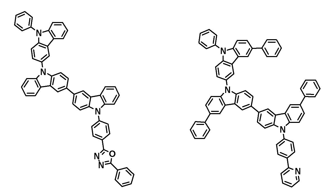
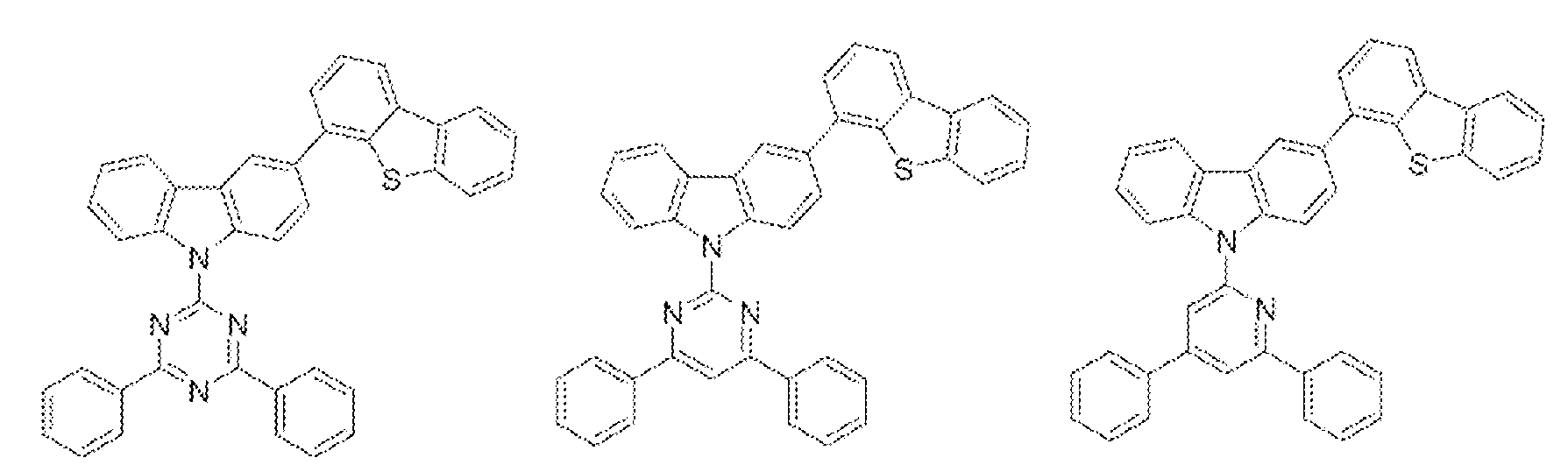
- the compound for an organic optoelectronic device may be represented by any one of the following Formulas A-2 to A-26, but is not limited thereto.
- the compound for an organic optoelectronic device may be represented by any one of the following Formulas B-3 to B-22, but is not limited thereto.
- the compound for an organic optoelectronic device may be represented by any one of the following Chemical Formulas C-1 to C-18, but is not limited thereto.
- the compound for an organic optoelectronic device including the compound as described above has a glass transition temperature of 110 ° C. or more, and a thermal decomposition temperature of 400 ° C. or more, which is excellent in thermal stability. This enables the implementation of high efficiency organic optoelectronic devices.
- the compound for an organic optoelectronic device including the compound as described above may serve as light emission, electron injection and / or transport, and may also serve as a light emitting host with an appropriate dopant. That is, the compound for an organic optoelectronic device may be used as a host material of phosphorescence or fluorescence, a blue dopant material, or an electron transport material.
- Compound for an organic optoelectronic device according to an embodiment of the present invention is used in the organic thin film layer to improve the life characteristics, efficiency characteristics, electrochemical stability and thermal stability of the organic optoelectronic device, it is possible to lower the driving voltage.
- one embodiment of the present invention provides an organic optoelectronic device comprising the compound for an organic optoelectronic device.
- the organic photoelectric device means an organic photoelectric device, an organic light emitting device, an organic solar cell, an organic transistor, an organic photosensitive drum, an organic memory device, or the like.
- a compound for an organic optoelectronic device according to an embodiment of the present invention is included in an electrode or an electrode buffer layer to increase quantum efficiency, and in the case of an organic transistor, a gate, a source-drain electrode, or the like may be used as an electrode material. Can be used.
- Another embodiment of the present invention is an organic light emitting device comprising an anode, a cathode and at least one organic thin film layer interposed between the anode and the cathode, at least one of the organic thin film layer is an embodiment of the present invention It provides an organic light emitting device comprising a compound for an organic optoelectronic device according to.
- the organic thin film layer which may include the compound for an organic optoelectronic device may include a layer selected from the group consisting of a light emitting layer, a hole transport layer, a hole injection layer, an electron transport layer, an electron injection layer, a hole blocking layer and a combination thereof. At least one of the layers includes the compound for an organic optoelectronic device according to the present invention.
- the electron transport layer or the electron injection layer may include a compound for an organic optoelectronic device according to an embodiment of the present invention.
- the compound for an organic optoelectronic device when included in a light emitting layer, the compound for an organic optoelectronic device may be included as a phosphorescent or fluorescent host, and in particular, may be included as a fluorescent blue dopant material.
- FIG. 1 to 5 are cross-sectional views of an organic light emitting device including a compound for an organic optoelectronic device according to an embodiment of the present invention.
- the organic photoelectric device 100, 200, 300, 400, and 500 may be interposed between the anode 120, the cathode 110, and the anode and the cathode. It has a structure including at least one organic thin film layer 105.
- the anode 120 includes a cathode material, and a material having a large work function is preferable as the anode material so that hole injection can be smoothly injected into the organic thin film layer.
- the positive electrode material include metals such as nickel, platinum, vanadium, chromium, copper, zinc, and gold or alloys thereof, and include zinc oxide, indium oxide, indium tin oxide (ITO), and indium zinc oxide (IZO).
- metal oxides such as ZnO and Al, or combinations of metals and oxides such as SnO 2 and Sb, and poly (3-methylthiophene), poly [3,4- (ethylene-1, 2-dioxy) thiophene] (conductive polymers such as polyehtylenedioxythiophene (PEDT), polypyrrole and polyaniline, etc.), but is not limited thereto.
- a transparent electrode including indium tin oxide (ITO) may be used as the anode.
- the negative electrode 110 includes a negative electrode material, and the negative electrode material is preferably a material having a small work function to facilitate electron injection into the organic thin film layer.
- the negative electrode material include metals such as magnesium, calcium, sodium, potassium, titanium, indium, yttrium, lithium, gadolinium, aluminum, silver, tin, lead, cesium, barium, or alloys thereof, and LiF / Al.
- Multilayer structure materials such as LiO 2 / Al, LiF / Ca, LiF / Al, and BaF 2 / Ca, and the like, but are not limited thereto.
- a metal electrode such as aluminum may be used as the cathode.
- FIG. 1 illustrates an organic photoelectric device 100 in which only a light emitting layer 130 exists as an organic thin film layer 105.
- the organic thin film layer 105 may exist only as a light emitting layer 130.
- FIG. 2 illustrates a two-layered organic photoelectric device 200 in which an emission layer 230 including an electron transport layer and a hole transport layer 140 exist as an organic thin film layer 105, as shown in FIG. 2.
- the organic thin film layer 105 may be a two-layer type including the light emitting layer 230 and the hole transport layer 140.
- the light emitting layer 130 functions as an electron transporting layer
- the hole transporting layer 140 functions to improve bonding and hole transporting properties with a transparent electrode such as ITO.
- FIG. 3 is a three-layered organic photoelectric device 300 having an electron transport layer 150, an emission layer 130, and a hole transport layer 140 as an organic thin film layer 105, wherein the organic thin film layer 105 is formed.
- the light emitting layer 130 is in an independent form, and has a form in which a film (electron transport layer 150 and hole transport layer 140) having excellent electron transport properties or hole transport properties is stacked in separate layers.
- FIG. 4 is a four-layered organic photoelectric device 400 having an electron injection layer 160, a light emitting layer 130, a hole transport layer 140, and a hole injection layer 170 as an organic thin film layer 105.
- the hole injection layer 170 may improve adhesion to ITO used as an anode.
- FIG. 5 shows different functions such as the electron injection layer 160, the electron transport layer 150, the light emitting layer 130, the hole transport layer 140, and the hole injection layer 170 as the organic thin film layer 105.
- the five-layered organic photoelectric device 500 having five layers is present, and the organic photoelectric device 500 is effective for lowering the voltage by forming the electron injection layer 160 separately.
- the electron transport layer 150, the electron injection layer 160, the light emitting layers 130 and 230, the hole transport layer 140, and the hole injection layer 170 forming the organic thin film layer 105 and their Any one selected from the group consisting of a combination includes the compound for an organic optoelectronic device.
- the compound for an organic optoelectronic device may be used in the electron transport layer 150 including the electron transport layer 150 or the electron injection layer 160, and among them, a hole blocking layer (not shown) when included in the electron transport layer. It is desirable to provide an organic photoelectric device having a simpler structure since it does not need to be separately formed.
- the compound for an organic photoelectric device when included in the light emitting layers 130 and 230, the compound for an organic photoelectric device may be included as a phosphorescent or fluorescent host, or may be included as a fluorescent blue dopant.
- the organic light emitting device described above may include a dry film method such as vacuum deposition, sputtering, plasma plating, and ion plating after an anode is formed on a substrate;
- the organic thin film layer may be formed by a wet film method such as spin coating, dipping, flow coating, or the like, followed by forming a cathode thereon.
- a display device including the organic photoelectric device is provided.
- the obtained compound represented by Chemical Formula 4 was analyzed by elemental analysis. The results were as follows.
- the obtained compound represented by Chemical Formula 5 was analyzed by elemental analysis. The results were as follows.
- the obtained compound represented by Chemical Formula 14 was analyzed by elemental analysis. The results were as follows.
- reaction mixture was poured into methanol, and the solid was filtered. Then, the solid was dissolved in chlorobenzene, and then activated carbon and anhydrous magnesium sulfate were stirred. The solution was filtered and recrystallized with chlorobenzene and methanol to obtain compound A-10 11g (84% yield).
- An organic light emitting diode was manufactured by using the compound synthesized in Example 1 as a host and using Ir (PPy) 3 as a dopant.
- ITO was used as a cathode of 1000 kPa
- aluminum (Al) was used as a cathode of 1000 kPa.
- the manufacturing method of the organic light emitting device is 15 ⁇ / cm 2
- the ITO glass substrate having a sheet resistance of was cut into a size of 50 mm ⁇ 50 mm ⁇ 0.7 mm, ultrasonically cleaned in acetone, isopropyl alcohol, and pure water for 15 minutes, and then UV ozone cleaned for 30 minutes.
- N, N'-di (1-naphthyl) -N, N'-diphenylbenzidine (NPB) 70 nm
- NPB N, N'-di (1-naphthyl) -N, N'-diphenylbenzidine
- TCTA 4,4 ', 4 "-tri (N-carbazolyl) triphenylamine
- a light emitting layer having a film thickness of 300 Pa was formed using the compound synthesized in Example 2 under the same vacuum deposition conditions.
- Ir (PPy) 3 which is a phosphorescent dopant, was simultaneously deposited.
- the deposition rate of the phosphorescent dopant was deposited so as to be 7% by weight.
- Bis (8-hydroxy-2-methylquinolinato) -aluminum biphenoxide (BAlq) was deposited on the light emitting layer using the same vacuum deposition conditions to form a hole blocking layer having a thickness of 50 kHz.
- Alq 3 was deposited under the same vacuum deposition conditions to form an electron transport layer having a film thickness of 200 GPa.
- An organic photoelectric device was manufactured by sequentially depositing LiF and Al as a cathode on the electron transport layer.
- the structure of the organic photoelectric device is ITO / NPB (70 nm) / TCTA (10 nm) / EML (compound of Example 1 (93% by weight) + Ir (PPy) 3 (7% by weight), 30 nm) / Balq (5 nm) / Alq 3 (20 nm) / LiF (1 nm) / Al (100 nm).
- An organic light emitting diode was manufactured according to the same method as Example 13 except for using the compound synthesized in Example 2 as a host of the light emitting layer, instead of using the compound synthesized in Example 1 as a host of the light emitting layer.
- An organic light emitting diode was manufactured according to the same method as Example 13 except for using the compound synthesized in Example 4 as a host of the light emitting layer, instead of using the compound synthesized in Example 1 as a host of the light emitting layer.
- An organic light emitting diode was manufactured according to the same method as Example 13 except for using the compound synthesized in Example 6 as a host of the light emitting layer, instead of using the compound synthesized in Example 1 as a host of the light emitting layer.
- An organic light emitting diode was manufactured according to the same method as Example 13 except for using the compound synthesized in Example 7 as a host of the light emitting layer, instead of using the compound synthesized in Example 1 as a host of the light emitting layer.
- An organic light emitting diode was manufactured according to the same method as Example 13 except for using the compound synthesized in Example 10 as a host of the light emitting layer, instead of using the compound synthesized in Example 1 as a host of the light emitting layer.
- An organic light emitting diode was manufactured according to the same method as Example 13 except for using the compound synthesized in Example 11 as a host of the light emitting layer, instead of using the compound synthesized in Example 1 as a host of the light emitting layer.
- An organic light emitting diode was manufactured according to the same method as Example 13 except for using the compound synthesized in Example 12 as a host of the light emitting layer, instead of using the compound synthesized in Example 1 as a host of the light emitting layer.
- Example 2 Except for using the compound synthesized in Example 2 as the host of the light emitting layer, the same as in Example 13 except that 4,4-N, N-dicarbazole biphenyl (CBP) was used as the host of the light emitting layer An organic light emitting device was manufactured by the method.
- CBP N-dicarbazole biphenyl
- the current value flowing through the unit device was measured using a current-voltmeter (Keithley 2400) while increasing the voltage from 0 V to 10 V, and the measured current value was divided by the area to obtain a result.
- the resulting organic light emitting device was measured by using a luminance meter (Minolta Cs-1000A) while increasing the voltage from 0 V to 10 V to obtain a result.
- a luminance meter Minolta Cs-1000A
- the current efficiency (cd / A) of the same brightness (9000 cd / m 2 ) was calculated using the brightness, current density, and voltage measured from (1) and (2) above.
- Example 1 Host material of light emitting layer Threshold voltage (V) 9000 cd / m2 Luminous Efficiency (cd / A) Life (h, T97%) Example 13
- Example 1 4.1 87.9 50
- Example 14 Example 2 4.3 88.7 50
- Example 15 Example 4 4.1 83.8 45
- Example 16 Example 6 4.7 73.7 20
- Example 17 Example 7 5.1 73.6 10
- Example 18 Example 10 4.8 78.7 60
- Example 19 Example 11 4.0 68.2 10
- Example 20 Example 12 5.3 69.5 5 Comparative Example 1 CBP 4.8 31.4 ⁇ 1 Comparative Example 2 Bis [9- (4-methoxyphenyl) carbazol-3-yl] - 30 to 35 -
- the device manufactured using the material provided in the present invention is much superior in driving voltage and efficiency in comparison with CBP, which is a reference material, in luminous efficiency.
- the lifetime was measured until the 3% luminous efficiency was reduced.
- CBP the lifespan was suddenly less than 1 hour, but in the case of a device manufactured using the compound provided in the present invention, Life spans up to 60 hours.
- organic photoelectric device 110 cathode
- hole injection layer 230 light emitting layer + electron transport layer
Landscapes
- Chemical & Material Sciences (AREA)
- Organic Chemistry (AREA)
- Engineering & Computer Science (AREA)
- Materials Engineering (AREA)
- Physics & Mathematics (AREA)
- Spectroscopy & Molecular Physics (AREA)
- Optics & Photonics (AREA)
- Electroluminescent Light Sources (AREA)
- Plural Heterocyclic Compounds (AREA)
- Organic Low-Molecular-Weight Compounds And Preparation Thereof (AREA)
Abstract
Description


| 발광층의 호스트 재료 | 문턱전압(V) | 9000 cd/m2 | ||
| 발광효율(cd/A) | 수명(h, T97%) | |||
| 실시예 13 | 실시예 1 | 4.1 | 87.9 | 50 |
| 실시예 14 | 실시예 2 | 4.3 | 88.7 | 50 |
| 실시예 15 | 실시예 4 | 4.1 | 83.8 | 45 |
| 실시예 16 | 실시예 6 | 4.7 | 73.7 | 20 |
| 실시예 17 | 실시예 7 | 5.1 | 73.6 | 10 |
| 실시예 18 | 실시예 10 | 4.8 | 78.7 | 60 |
| 실시예 19 | 실시예 11 | 4.0 | 68.2 | 10 |
| 실시예 20 | 실시예 12 | 5.3 | 69.5 | 5 |
| 비교예 1 | CBP | 4.8 | 31.4 | < 1 |
| 비교예 2 | 비스[9-(4-메톡시페닐)카바졸-3-일] | - | 30 내지 35 | - |
Claims (28)
- 하기 화학식 1로 표시되는 유기광전자소자용 화합물:[화학식 1]
 상기 화학식 1에서,X1 및 X2는 서로 동일하거나 상이하며, 독립적으로 -NR'-, -O-, -Se-, -P- 및 -S- 로 이루어진 군에서 선택되고,상기 R'는 수소, 중수소, 치환 또는 비치환된 C1 내지 C20 알킬기, 치환 또는 비치환된 C6 내지 C30 아릴기 및 전자 특성을 가지는, 치환 또는 비치환된 C2 내지 C30 헤테로아릴기로 이루어진 군에서 선택되고,상기 R1 내지 R6는 서로 동일하거나 상이하며, 독립적으로 수소, 중수소, 치환 또는 비치환된 C1 내지 C20 알킬기, 치환 또는 비치환된 C6 내지 C30 아릴기 및 전자 특성을 가지는, 치환 또는 비치환된 C2 내지 C30 헤테로아릴기로 이루어진 군에서 선택되고,상기 R1 내지 R6 또는 R' 중 적어도 어느 하나는 전자 특성을 가지는, 치환 또는 비치환된 C2 내지 C30 헤테로아릴기다.
 - 제 1 항에 있어서,상기 유기광전자소자용 화합물은 하기 화학식 2로 표시되는 것인 유기광전자소자용 화합물:[화학식 2]
 상기 화학식 2에서,X1 및 X2는 서로 동일하거나 상이하며, 독립적으로 -NR'-, -O-, -Se-, -P- 및 -S- 로 이루어진 군에서 선택되고,상기 R'는 수소, 중수소, 치환 또는 비치환된 C1 내지 C20 알킬기, 치환 또는 비치환된 C6 내지 C30 아릴기 및 전자 특성을 가지는, 치환 또는 비치환된 C2 내지 C30 헤테로아릴기로 이루어진 군에서 선택되고,상기 R1 내지 R6는 서로 동일하거나 상이하며, 독립적으로 수소, 중수소, 치환 또는 비치환된 C1 내지 C20 알킬기, 치환 또는 비치환된 C6 내지 C30 아릴기 및 전자 특성을 가지는, 치환 또는 비치환된 C2 내지 C30 헤테로아릴기로 이루어진 군에서 선택되고,상기 R1 내지 R6 또는 R' 중 적어도 어느 하나는 전자 특성을 가지는, 치환 또는 비치환된 C2 내지 C30 헤테로아릴기다.
 - 제 1 항에 있어서,상기 X1은 -NR'-인 것인 유기광전자소자용 화합물:상기 R'는 수소, 중수소, 치환 또는 비치환된 C1 내지 C20 알킬기, 치환 또는 비치환된 C6 내지 C30 아릴기 및 전자 특성을 가지는, 치환 또는 비치환된 C2 내지 C30 헤테로아릴기로 이루어진 군에서 선택된다.
- 제 3 항에 있어서,상기 R'는 전자 특성을 가지는, 치환 또는 비치환된 C2 내지 C30 헤테로아릴기인 것인 유기광전자소자용 화합물.
- 제 1 항에 있어서,X1는 -NR'-이고,상기 R'는 전자 특성을 가지는, 치환 또는 비치환된 C2 내지 C30 헤테로아릴기고,상기 R1 내지 R6는 서로 동일하거나 상이하며, 독립적으로 수소, 중수소, 치환 또는 비치환된 C1 내지 C20 알킬기 및 치환 또는 비치환된 C6 내지 C30 아릴기로 이루어진 군에서 선택되는 것인 유기광전자소자용 화합물.
- 제 1 항에 있어서,상기 전자 특성을 가지는, 치환 또는 비치환된 C2 내지 C30 헤테로아릴기는 치환 또는 비치환된 이미다졸릴기, 치환 또는 비치환된 트리아졸릴기, 치환 또는 비치환된 테트라졸릴기, 치환 또는 비치환된 옥사다이아졸릴기, 치환 또는 비치환된 옥사트리아졸릴기, 치환 또는 비치환된 싸이아트리아졸릴기, 치환 또는 비치환된 벤즈이미다졸릴기, 치환 또는 비치환된 벤조트리아졸릴기, 치환 또는 비치환된 피리디닐기, 치환 또는 비치환된 피리미디닐기, 치환 또는 비치환된 트리아지닐기, 치환 또는 비치환된 피라지닐기, 치환 또는 비치환된 피리다지닐기, 치환 또는 비치환된 퓨리닐기, 치환 또는 비치환된 퀴놀리닐기, 치환 또는 비치환된 이소퀴놀리닐기, 치환 또는 비치환된 프탈라지닐기, 치환 또는 비치환된 나프피리디닐기, 치환 또는 비치환된 퀴녹살리닐기, 치환 또는 비치환된 퀴나졸리닐기, 치환 또는 비치환된 아크리디닐기, 치환 또는 비치환된 페난트롤리닐기 및 치환 또는 비치환된 페나지닐기으로 이루어진 군에서 선택되는 것인 유기광전자소자용 화합물.
- 하기 화학식 3 내지 54 중 어느 하나로 표시되는 유기광전자소자용 화합물.[화학식 3] [화학식 4]
 [화학식 5] [화학식 6]
 [화학식 7] [화학식 8]
 [화학식 9] [화학식 10]
 [화학식 11] [화학식 12]
 [화학식 13] [화학식 14]
 [화학식 15] [화학식 16]
 [화학식 17] [화학식 18]
 [화학식 19] [화학식 20]
 [화학식 21] [화학식 22]
 [화학식 23] [화학식 24]
 [화학식 25] [화학식 26]
 [화학식 27] [화학식 28]
 [화학식 29] [화학식 30]
 [화학식 31] [화학식 32]
 [화학식 33] [화학식 34]
 [화학식 35] [화학식 36]
 [화학식 37] [화학식 38]
 [화학식 39] [화학식 40]
 [화학식 41] [화학식 42]
 [화학식 43] [화학식 44]
 [화학식 45] [화학식 46]
 [화학식 47] [화학식 48]
 [화학식 49] [화학식 50]
 [화학식 51] [화학식 52]
 [화학식 53] [화학식 54]
- 제 1 항에 있어서,상기 유기광전자소자용 화합물은 하기 화학식 A 또는 A-1로 표시되는 것인 유기광전자소자용 화합물:[화학식 A]
 [화학식 A-1]
 상기 화학식 A 및 A-1에서,X1 및 X2는 서로 동일하거나 상이하며, 독립적으로 -NR'-, -O-, -Se-, -P- 및 -S- 로 이루어진 군에서 선택되고,상기 R'는 수소, 중수소, 치환 또는 비치환된 C1 내지 C20 알킬기, 치환 또는 비치환된 C6 내지 C30 아릴기 및 전자 특성을 가지는, 치환 또는 비치환된 C2 내지 C30 헤테로아릴기로 이루어진 군에서 선택되고,상기 R1 내지 R6는 서로 동일하거나 상이하며, 독립적으로 수소, 중수소, 치환 또는 비치환된 C1 내지 C20 알킬기, 치환 또는 비치환된 C6 내지 C30 아릴기 및 전자 특성을 가지는, 치환 또는 비치환된 C2 내지 C30 헤테로아릴기로 이루어진 군에서 선택되고,상기 R1 내지 R6 또는 R' 중 적어도 어느 하나는 전자 특성을 가지는, 치환 또는 비치환된 C2 내지 C30 헤테로아릴기다.
 - 제 8 항에 있어서,상기 X1 또는 X2 중 적어도 하나는 -NR'-이고,상기 R'는 전자 특성을 가지는, 치환 또는 비치환된 C2 내지 C30 헤테로아릴기고,상기 R1 내지 R6는 서로 동일하거나 상이하며, 독립적으로 수소, 중수소, 치환 또는 비치환된 C1 내지 C20 알킬기 및 치환 또는 비치환된 C6 내지 C30 아릴기로 이루어진 군에서 선택되는 것인 유기광전자소자용 화합물.
- 제 8 항에 있어서,상기 X1 또는 X2 중 적어도 하나는 -NR'-이고,상기 R'는 치환 또는 비치환된 트리페닐레닐기인 것인 유기광전자소자용 화합물.
- 제 8 항에 있어서,상기 전자 특성을 가지는, 치환 또는 비치환된 C2 내지 C30 헤테로아릴기는 치환 또는 비치환된 이미다졸릴기, 치환 또는 비치환된 트리아졸릴기, 치환 또는 비치환된 테트라졸릴기, 치환 또는 비치환된 옥사다이아졸릴기, 치환 또는 비치환된 옥사트리아졸릴기, 치환 또는 비치환된 싸이아트리아졸릴기, 치환 또는 비치환된 벤즈이미다졸릴기, 치환 또는 비치환된 벤조트리아졸릴기, 치환 또는 비치환된 피리디닐기, 치환 또는 비치환된 피리미디닐기, 치환 또는 비치환된 트리아지닐기, 치환 또는 비치환된 피라지닐기, 치환 또는 비치환된 피리다지닐기, 치환 또는 비치환된 퓨리닐기, 치환 또는 비치환된 퀴놀리닐기, 치환 또는 비치환된 이소퀴놀리닐기, 치환 또는 비치환된 프탈라지닐기, 치환 또는 비치환된 나프피리디닐기, 치환 또는 비치환된 퀴녹살리닐기, 치환 또는 비치환된 퀴나졸리닐기, 치환 또는 비치환된 아크리디닐기, 치환 또는 비치환된 페난트롤리닐기 및 치환 또는 비치환된 페나지닐기으로 이루어진 군에서 선택되는 것인 유기광전자소자용 화합물.
- 제 8 항에 있어서,상기 유기광전자소자용 화합물은 하기 화학식 A-2 내지 A-26 중 어느 하나로 표시되는 것인 유기광전자소자용 화합물.[화학식 A-2] [화학식 A-3]
 [화학식 A-4] [화학식 A-5]
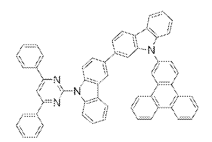
 [화학식 A-6] [화학식 A-7]
 [화학식 A-8] [화학식 A-9]
 [화학식 A-10] [화학식 A-11]
 [화학식 A-12] [화학식 A-13]
 [화학식 A-14] [화학식 A-15]
 [화학식 A-16] [화학식 A-17]
 [화학식 A-18] [화학식 A-19]
 [화학식 A-20] [화학식 A-21]
 [화학식 A-22] [화학식 A-23]
 [화학식 A-24] [화학식 A-25]
 [화학식 A-26]
- 제 1 항에 있어서,상기 유기광전자소자용 화합물은 하기 화학식 B로 표시되는 것인 유기광전자소자용 화합물:[화학식 B]
 상기 화학식 B에서,X1은 -O-, -Se-, -P- 및 -S- 로 이루어진 군에서 선택되고,R1 내지 R6는 서로 동일하거나 상이하며, 독립적으로 수소, 중수소, 치환 또는 비치환된 C1 내지 C20 알킬기, 치환 또는 비치환된 C6 내지 C30 아릴기 및 치환 또는 비치환된 C2 내지 C30 헤테로아릴기로 이루어진 군에서 선택되고,Ar은 전자 특성을 가지는, 치환 또는 비치환된 C2 내지 C30 헤테로아릴기이고,L은 단일결합, 치환 또는 비치환된 C2 내지 C10 알케닐렌기, 치환 또는 비치환된 C2 내지 C10 알키닐렌기, 치환 또는 비치환된 C6 내지 C30 아릴렌기 및 치환 또는 비치환된 C2 내지 C30 헤테로아릴렌기로 이루어진 군에서 선택되고,n은 0 내지 2 중 어느 하나의 정수이다.
 - 제 13 항에 있어서,상기 유기광전자소자용 화합물은 하기 화학식 B-1 또는 B-2로 표시되는 것인 유기광전자소자용 화합물:[화학식 B-1]
 [화학식 B-2]
 상기 화학식 B-1 및 B-2에 있어서,X1은 -O-, -Se-, -P- 및 -S- 로 이루어진 군에서 선택되고,R1 내지 R6는 서로 동일하거나 상이하며, 독립적으로 수소, 중수소, 치환 또는 비치환된 C1 내지 C20 알킬기, 치환 또는 비치환된 C6 내지 C30 아릴기 및 치환 또는 비치환된 C2 내지 C30 헤테로아릴기로 이루어진 군에서 선택되고,Ar은 전자 특성을 가지는, 치환 또는 비치환된 C2 내지 C30 헤테로아릴기이고,L은 단일결합, 치환 또는 비치환된 C2 내지 C10 알케닐렌기, 치환 또는 비치환된 C2 내지 C10 알키닐렌기, 치환 또는 비치환된 C6 내지 C30 아릴렌기 및 치환 또는 비치환된 C2 내지 C30 헤테로아릴렌기로 이루어진 군에서 선택되고,n은 0 내지 2 중 어느 하나의 정수이다.
 - 제 13 항에 있어서,상기 전자 특성을 가지는, 치환 또는 비치환된 C2 내지 C30 헤테로아릴기는 치환 또는 비치환된 이미다졸릴기, 치환 또는 비치환된 트리아졸릴기, 치환 또는 비치환된 테트라졸릴기, 치환 또는 비치환된 옥사다이아졸릴기, 치환 또는 비치환된 옥사트리아졸릴기, 치환 또는 비치환된 싸이아트리아졸릴기, 치환 또는 비치환된 벤즈이미다졸릴기, 치환 또는 비치환된 벤조트리아졸릴기, 치환 또는 비치환된 피리디닐기, 치환 또는 비치환된 피리미디닐기, 치환 또는 비치환된 트리아지닐기, 치환 또는 비치환된 피라지닐기, 치환 또는 비치환된 피리다지닐기, 치환 또는 비치환된 퓨리닐기, 치환 또는 비치환된 퀴놀리닐기, 치환 또는 비치환된 이소퀴놀리닐기, 치환 또는 비치환된 프탈라지닐기, 치환 또는 비치환된 나프피리디닐기, 치환 또는 비치환된 퀴녹살리닐기, 치환 또는 비치환된 퀴나졸리닐기, 치환 또는 비치환된 아크리디닐기, 치환 또는 비치환된 페난트롤리닐기 및 치환 또는 비치환된 페나지닐기으로 이루어진 군에서 선택되는 것인 유기광전자소자용 화합물.
- 제 13 항에 있어서,상기 유기광전자소자용 화합물은 하기 화학식 B-3 내지 B-22 중 어느 하나로 표시되는 것인 유기광전자소자용 화합물.[화학식 B-3] [화학식 B-4] [화학식 B-5]
 [화학식 B-6] [화학식 B-7] [화학식 B-8]
 [화학식 B-9] [화학식 B-10] [화학식 B-11]
 [화학식 B-12] [화학식 B-13] [화학식 B-14]
 [화학식 B-15] [화학식 B-16] [화학식 B-17]
 [화학식 B-18] [화학식 B-19] [화학식 B-20]
 [화학식 B-21] [화학식 B-22]
- 제 1 항에 있어서,상기 유기광전자소자용 화합물은 하기 화학식 C로 표시되는 것인 유기광전자소자용 화합물:[화학식 C]
 상기 화학식 C에 있어서,R1 내지 R6 및 Ar2는 서로 동일하거나 상이하며, 독립적으로 수소, 중수소, 치환 또는 비치환된 C1 내지 C20 알킬기, 치환 또는 비치환된 C6 내지 C30 아릴기 및 치환 또는 비치환된 C2 내지 C30 헤테로아릴기로 이루어진 군에서 선택되고,Ar1은 전자 특성을 가지는, 치환 또는 비치환된 C2 내지 C30 헤테로아릴기이고,L은 단일결합, 치환 또는 비치환된 C2 내지 C10 알케닐렌기, 치환 또는 비치환된 C2 내지 C10 알키닐렌기, 치환 또는 비치환된 C6 내지 C30 아릴렌기 및 치환 또는 비치환된 C2 내지 C30 헤테로아릴렌기로 이루어진 군에서 선택되고,n은 1 또는 2이다.
 - 제 17 항에 있어서,상기 Ar2는 치환 또는 비치환된 트리페닐레닐기인 것인 유기광전자소자용 화합물.
- 제 17 항에 있어서,상기 전자 특성을 가지는, 치환 또는 비치환된 C2 내지 C30 헤테로아릴기는 치환 또는 비치환된 이미다졸릴기, 치환 또는 비치환된 트리아졸릴기, 치환 또는 비치환된 테트라졸릴기, 치환 또는 비치환된 옥사다이아졸릴기, 치환 또는 비치환된 옥사트리아졸릴기, 치환 또는 비치환된 싸이아트리아졸릴기, 치환 또는 비치환된 벤즈이미다졸릴기, 치환 또는 비치환된 벤조트리아졸릴기, 치환 또는 비치환된 피리디닐기, 치환 또는 비치환된 피리미디닐기, 치환 또는 비치환된 트리아지닐기, 치환 또는 비치환된 피라지닐기, 치환 또는 비치환된 피리다지닐기, 치환 또는 비치환된 퓨리닐기, 치환 또는 비치환된 퀴놀리닐기, 치환 또는 비치환된 이소퀴놀리닐기, 치환 또는 비치환된 프탈라지닐기, 치환 또는 비치환된 나프피리디닐기, 치환 또는 비치환된 퀴녹살리닐기, 치환 또는 비치환된 퀴나졸리닐기, 치환 또는 비치환된 아크리디닐기, 치환 또는 비치환된 페난트롤리닐기 및 치환 또는 비치환된 페나지닐기으로 이루어진 군에서 선택되는 것인 유기광전자소자용 화합물.
- 제 17 항에 있어서,상기 유기광전자소자용 화합물은 하기 화학식 C-1 내지 C-18 중 어느 하나로 표시되는 것인 유기광전자소자용 화합물.[화학식 C-1] [화학식 C-2] [화학식 C-3]
 [화학식 C-4] [화학식 C-5] [화학식 C-6]
 [화학식 C-7] [화학식 C-8] [화학식 C-9]
 [화학식 C-10] [화학식 C-11] [화학식 C-12]
 [화학식 C-13] [화학식 C-14] [화학식 C-15]
 [화학식 C-16] [화학식 C-17] [화학식 C-18]
- 제 1 항에 있어서,상기 유기광전소자는, 유기광전소자, 유기발광소자, 유기태양전지, 유기트랜지스터, 유기 감광체 드럼 및 유기메모리소자로 이루어진 군에서 선택되는 것인 유기광전자소자용 화합물.
- 양극, 음극 및 상기 양극과 음극 사이에 개재되는 적어도 한 층 이상의 유기박막층을 포함하는 유기발광소자에 있어서,상기 유기박막층 중 적어도 어느 한 층은 상기 제 1 항에 따른 유기광전자소자용 화합물을 포함하는 것인 유기발광소자.
- 제 22 항에 있어서,상기 유기박막층은 발광층, 정공수송층, 정공주입층, 전자수송층, 전자주입층, 정공차단층 및 이들의 조합을 이루어진 군에서 선택되는 것인 유기발광소자.
- 제 22 항에 있어서,상기 유기광전자소자용 화합물은 전자수송층 또는 전자주입층 내에 포함되는 것인 유기발광소자.
- 제 22 항에 있어서,상기 유기광전자소자용 화합물은 발광층 내에 포함되는 것인 유기발광소자.
- 제 22 항에 있어서,상기 유기광전자소자용 화합물은 발광층 내에 인광 또는 형광 호스트 재료로서 사용되는 것인 유기발광소자.
- 제 22 항에 있어서,상기 유기광전자소자용 화합물은 발광층 내에 형광 청색 도펀트 재료로서 사용되는 것인 유기발광소자.
- 제 22 항의 유기발광소자를 포함하는 것인 표시장치.
Priority Applications (6)
| Application Number | Priority Date | Filing Date | Title |
|---|---|---|---|
| EP19155683.6A EP3514846B1 (en) | 2010-05-03 | 2011-04-29 | Compound for organic optoelectronic device, organic light emitting diode including same, and display device including the organic light emitting diode |
| EP11777536.1A EP2568030B1 (en) | 2010-05-03 | 2011-04-29 | Compound for organic optoelectronic device, organic light emitting diode including same, and display device including organic light emitting diode |
| EP19155679.4A EP3509121B1 (en) | 2010-05-03 | 2011-04-29 | Compound for organic optoelectronic device, organic light emitting diode including same, and display device including the organic light emitting diode |
| CN201180022469.XA CN102971395B (zh) | 2010-05-03 | 2011-04-29 | 用于有机光电子装置的化合物、包含其的有机发光二极管和包含所述有机发光二极管的显示器 |
| JP2013508986A JP5938397B2 (ja) | 2010-05-03 | 2011-04-29 | 有機光電子素子用化合物、これを含む有機発光ダイオードおよび前記有機発光ダイオードを含む表示装置 |
| US13/668,550 US9543530B2 (en) | 2010-05-03 | 2012-11-05 | Compound for organic optoelectronic device, organic light emitting diode including the same and display including the organic light emitting diode |
Applications Claiming Priority (4)
| Application Number | Priority Date | Filing Date | Title |
|---|---|---|---|
| KR20100041466 | 2010-05-03 | ||
| KR10-2010-0041466 | 2010-05-03 | ||
| KR10-2010-0106077 | 2010-10-28 | ||
| KR1020100106077A KR20110122051A (ko) | 2010-05-03 | 2010-10-28 | 유기광전소자용 화합물 및 이를 포함하는 유기광전소자 |
Related Child Applications (1)
| Application Number | Title | Priority Date | Filing Date |
|---|---|---|---|
| US13/668,550 Continuation-In-Part US9543530B2 (en) | 2010-05-03 | 2012-11-05 | Compound for organic optoelectronic device, organic light emitting diode including the same and display including the organic light emitting diode |
Publications (2)
| Publication Number | Publication Date |
|---|---|
| WO2011139055A2 true WO2011139055A2 (ko) | 2011-11-10 |
| WO2011139055A3 WO2011139055A3 (ko) | 2012-04-19 |
Family
ID=45392753
Family Applications (1)
| Application Number | Title | Priority Date | Filing Date |
|---|---|---|---|
| PCT/KR2011/003235 Ceased WO2011139055A2 (ko) | 2010-05-03 | 2011-04-29 | 유기광전자소자용 화합물, 이를 포함하는 유기발광소자 및 상기 유기발광소자를 포함하는 표시장치 |
Country Status (6)
| Country | Link |
|---|---|
| US (1) | US9543530B2 (ko) |
| EP (3) | EP2568030B1 (ko) |
| JP (1) | JP5938397B2 (ko) |
| KR (1) | KR20110122051A (ko) |
| CN (1) | CN102971395B (ko) |
| WO (1) | WO2011139055A2 (ko) |
Cited By (40)
| Publication number | Priority date | Publication date | Assignee | Title |
|---|---|---|---|---|
| JP2012087114A (ja) * | 2010-09-21 | 2012-05-10 | Semiconductor Energy Lab Co Ltd | カルバゾール誘導体、発光素子用材料及び有機半導体材料 |
| WO2012087007A1 (en) * | 2010-12-21 | 2012-06-28 | Rohm And Haas Electronic Materials Korea Ltd. | Novel organic electroluminescent compounds and organic electroluminescent device using the same |
| WO2012108388A1 (ja) * | 2011-02-07 | 2012-08-16 | 出光興産株式会社 | ビスカルバゾール誘導体及びそれを用いた有機エレクトロルミネッセンス素子 |
| WO2012124622A1 (ja) | 2011-03-14 | 2012-09-20 | 東レ株式会社 | 発光素子材料および発光素子 |
| WO2012128298A1 (ja) * | 2011-03-24 | 2012-09-27 | 出光興産株式会社 | ビスカルバゾール誘導体およびこれを用いた有機エレクトロルミネッセンス素子 |
| JP2012216801A (ja) * | 2011-03-28 | 2012-11-08 | Toray Ind Inc | 発光素子材料および発光素子 |
| WO2012153725A1 (ja) | 2011-05-12 | 2012-11-15 | 東レ株式会社 | 発光素子材料および発光素子 |
| JP2012530754A (ja) * | 2009-06-24 | 2012-12-06 | ジョージア・テック・リサーチ・コーポレーション | リン光ゲストエミッタのための両極性小分子ホスト |
| JP2012254971A (ja) * | 2011-05-13 | 2012-12-27 | Semiconductor Energy Lab Co Ltd | カルバゾール化合物、発光素子用材料、有機半導体材料 |
| EP2471771A4 (en) * | 2009-08-28 | 2013-01-16 | Hodogaya Chemical Co Ltd | ORGANIC ELECTROLUMINESCENE ELEMENT AND CONNECTION WITH A CARBAZOLERING STRUCTURE |
| WO2013012298A1 (en) * | 2011-07-21 | 2013-01-24 | Rohm And Haas Electronic Materials Korea Ltd. | 9h-carbazole compounds and electroluminescent devices involving them |
| JP2013116975A (ja) * | 2011-12-02 | 2013-06-13 | Kyushu Univ | 遅延蛍光材料、有機発光素子および化合物 |
| WO2013085243A1 (en) * | 2011-12-05 | 2013-06-13 | Rohm And Haas Electronic Materials Korea Ltd. | Novel organic electroluminescent compounds and organic electroluminescent device using the same |
| WO2013122082A1 (ja) * | 2012-02-15 | 2013-08-22 | 東レ株式会社 | 発光素子材料および発光素子 |
| WO2013133224A1 (ja) * | 2012-03-05 | 2013-09-12 | 東レ株式会社 | 発光素子 |
| JP2013536196A (ja) * | 2010-08-20 | 2013-09-19 | ユニバーサル ディスプレイ コーポレイション | Oledのためのビカルバゾール化合物 |
| WO2013157367A1 (ja) * | 2012-04-18 | 2013-10-24 | 保土谷化学工業株式会社 | 新規なトリフェニレン誘導体及び該誘導体が使用されている有機エレクトロルミネッセンス素子 |
| WO2013191177A1 (ja) * | 2012-06-18 | 2013-12-27 | 東ソー株式会社 | 環状アジン化合物、その製造方法、及びそれを含有する有機電界発光素子 |
| WO2014017484A1 (ja) | 2012-07-25 | 2014-01-30 | 東レ株式会社 | 発光素子材料および発光素子 |
| KR20140018133A (ko) * | 2012-08-03 | 2014-02-12 | 가부시키가이샤 한도오따이 에네루기 켄큐쇼 | 발광 소자 |
| JP2014028774A (ja) * | 2012-07-31 | 2014-02-13 | Tosoh Corp | カルバゾール化合物、その製造法、及びその用途 |
| WO2014092083A1 (ja) * | 2012-12-10 | 2014-06-19 | 出光興産株式会社 | 有機エレクトロルミネッセンス素子 |
| CN103959502A (zh) * | 2011-12-02 | 2014-07-30 | 国立大学法人九州大学 | 有机发光元件及使用其的迟滞荧光材料以及化合物 |
| US8803134B2 (en) | 2011-02-07 | 2014-08-12 | Idemitsu Kosan Co., Ltd. | Biscarbazole derivatives and organic electroluminescence |
| JP2014521604A (ja) * | 2011-07-21 | 2014-08-28 | ローム・アンド・ハース・エレクトロニック・マテリアルズ・コリア・リミテッド | 9h−カルバゾール化合物およびそれらを含むエレクトロルミネセンス素子 |
| CN104254529A (zh) * | 2012-04-27 | 2014-12-31 | 罗门哈斯电子材料韩国有限公司 | 新有机电致发光化合物和包含该化合物的有机电致发光器件 |
| JP2015006995A (ja) * | 2012-06-18 | 2015-01-15 | 東ソー株式会社 | 環状アジン化合物、その製造方法、及びそれを含有する有機電界発光素子 |
| EP2752902A4 (en) * | 2011-11-22 | 2015-01-21 | Idemitsu Kosan Co | AROMATIC HETEROCYCLIC DERIVATIVE, MATERIAL FOR AN ORGANIC ELECTROLUMINESCENE ELEMENT AND ORGANIC ELECTROLUMINESCENE ELEMENT |
| US20160028025A1 (en) * | 2013-03-18 | 2016-01-28 | Idemitsu Kosan Co., Ltd. | Light-emitting device |
| JP2016048805A (ja) * | 2010-09-21 | 2016-04-07 | 株式会社半導体エネルギー研究所 | 発光素子、発光装置、照明装置、表示装置、電子機器 |
| JP2016532686A (ja) * | 2013-07-29 | 2016-10-20 | エルジー・ケム・リミテッド | 複素環化合物及びこれを含む有機発光素子 |
| US9543530B2 (en) | 2010-05-03 | 2017-01-10 | Cheil Industries, Inc. | Compound for organic optoelectronic device, organic light emitting diode including the same and display including the organic light emitting diode |
| US9590184B2 (en) | 2012-12-27 | 2017-03-07 | Samsung Display Co., Ltd. | Organic light-emitting diode |
| US9685614B2 (en) | 2012-01-10 | 2017-06-20 | Idemitsu Kosan Co., Ltd. | Material for organic electroluminescent element, and element using same |
| CN107325050A (zh) * | 2012-12-28 | 2017-11-07 | 出光兴产株式会社 | 有机电致发光元件 |
| US10043982B2 (en) | 2013-04-26 | 2018-08-07 | Semiconductor Energy Laboratory Co., Ltd. | Light-emitting element, light-emitting device, display device, electronic device, and lighting device |
| KR20200038232A (ko) * | 2020-04-03 | 2020-04-10 | 덕산네오룩스 주식회사 | 유기전기 소자용 화합물, 이를 이용한 유기전기소자 및 그 전자 장치 |
| US10651392B2 (en) | 2015-09-30 | 2020-05-12 | Samsung Electronics Co., Ltd. | Organic light-emitting device |
| KR20210007026A (ko) * | 2020-04-03 | 2021-01-19 | 덕산네오룩스 주식회사 | 유기전기 소자용 화합물, 이를 이용한 유기전기소자 및 그 전자 장치 |
| US11925113B2 (en) | 2018-04-24 | 2024-03-05 | Lg Chem, Ltd. | Heterocyclic compound and organic light emitting device comprising the same |
Families Citing this family (78)
| Publication number | Priority date | Publication date | Assignee | Title |
|---|---|---|---|---|
| JP5821635B2 (ja) * | 2010-06-24 | 2015-11-24 | 東レ株式会社 | 発光素子材料および発光素子 |
| US9133173B2 (en) * | 2010-10-15 | 2015-09-15 | Semiconductor Energy Laboratory Co., Ltd. | Carbazole compound, material for light-emitting element, organic semiconductor material, light-emitting element |
| CN103228647B (zh) * | 2010-11-24 | 2017-02-15 | 默克专利有限公司 | 用于有机电致发光器件的材料 |
| EP2662368A4 (en) | 2010-12-20 | 2014-06-25 | Idemitsu Kosan Co | AROMATIC HETEROCYCLIC DERIVATIVE AND ORGANIC ELECTROLUMINESCENT ELEMENT THEREWITH |
| KR20120109744A (ko) * | 2011-03-25 | 2012-10-09 | 롬엔드하스전자재료코리아유한회사 | 신규한 유기 전자재료용 화합물 및 이를 포함하는 유기 전계 발광 소자 |
| KR101443756B1 (ko) * | 2011-05-26 | 2014-09-23 | 제일모직 주식회사 | 유기광전자소자용 화합물, 이를 포함하는 유기발광소자 및 상기 유기발광소자를 포함하는 표시장치 |
| KR101354638B1 (ko) | 2011-06-20 | 2014-01-22 | 제일모직주식회사 | 유기광전자소자용 재료, 이를 포함하는 유기발광소자 및 상기 유기발광소자를 포함하는 표시장치 |
| JP6034005B2 (ja) * | 2011-08-03 | 2016-11-30 | 出光興産株式会社 | ビスカルバゾール誘導体およびこれを用いた有機エレクトロルミネッセンス素子 |
| KR20130020398A (ko) * | 2011-08-19 | 2013-02-27 | 제일모직주식회사 | 유기광전자소자용 화합물, 이를 포함하는 유기발광소자 및 상기 유기발광소자를 포함하는 표시장치 |
| CN103959503B (zh) * | 2011-12-05 | 2016-08-24 | 出光兴产株式会社 | 有机电致发光元件用材料以及有机电致发光元件 |
| EP2871222B1 (en) | 2012-07-04 | 2017-04-26 | Samsung SDI Co., Ltd. | Compound for organic optoelectric device, organic optoelectric device comprising same, and display apparatus comprising organic optoelectric device |
| KR101686076B1 (ko) * | 2012-07-04 | 2016-12-13 | 제일모직주식회사 | 유기발광소자용 조성물, 이를 포함하는 유기발광층 및 유기발광소자 |
| KR101497138B1 (ko) * | 2012-08-21 | 2015-02-27 | 제일모직 주식회사 | 유기광전자소자 및 이를 포함하는 표시장치 |
| JP2014072417A (ja) * | 2012-09-28 | 2014-04-21 | Idemitsu Kosan Co Ltd | 有機エレクトロルミネッセンス素子用材料及び有機エレクトロルミネッセンス素子 |
| KR101820865B1 (ko) | 2013-01-17 | 2018-01-22 | 삼성전자주식회사 | 유기광전자소자용 재료, 이를 포함하는 유기발광소자 및 상기 유기발광소자를 포함하는 표시장치 |
| KR102065656B1 (ko) * | 2013-02-19 | 2020-01-13 | 덕산네오룩스 주식회사 | 유기전기 소자용 화합물, 이를 이용한 유기전기소자 및 그 전자 장치 |
| JPWO2014185535A1 (ja) * | 2013-05-16 | 2017-02-23 | ダイキン工業株式会社 | フラーレン誘導体、及びn型半導体材料 |
| KR102162795B1 (ko) | 2013-06-07 | 2020-10-08 | 삼성디스플레이 주식회사 | 헤테로고리 화합물 및 이를 포함한 유기 발광 소자 |
| KR102117609B1 (ko) | 2013-06-26 | 2020-06-02 | 삼성디스플레이 주식회사 | 헤테로고리 화합물 및 이를 포함한 유기 발광 소자 |
| KR101566434B1 (ko) * | 2013-07-15 | 2015-11-06 | 삼성디스플레이 주식회사 | 유기 발광 장치 |
| KR102116496B1 (ko) | 2013-08-26 | 2020-05-29 | 삼성디스플레이 주식회사 | 유기 발광 소자 |
| KR101812581B1 (ko) | 2013-10-11 | 2017-12-27 | 제일모직 주식회사 | 유기광전자소자용 유기합화물, 유기 광전자 소자 및 표시 장치 |
| KR102140006B1 (ko) * | 2013-10-11 | 2020-07-31 | 에스에프씨 주식회사 | 유기발광 화합물 및 이를 포함하는 유기전계발광소자 |
| KR20150071624A (ko) * | 2013-12-18 | 2015-06-26 | 롬엔드하스전자재료코리아유한회사 | 유기 전계 발광 화합물 및 이를 포함하는 유기 전계 발광 소자 |
| WO2015115744A1 (ko) * | 2014-01-29 | 2015-08-06 | 삼성에스디아이 주식회사 | 전자수송보조층용 조성물, 전자수송보조층을 포함하는 유기 광전자 소자 및 표시 장치 |
| KR101846436B1 (ko) * | 2014-01-29 | 2018-04-06 | 제일모직 주식회사 | 전자수송보조층용 조성물, 전자수송보조층을 포함하는 유기 광전자 소자 및 표시 장치 |
| WO2015126081A1 (ko) * | 2014-02-21 | 2015-08-27 | 삼성에스디아이 주식회사 | 유기 광전자 소자 및 표시 장치 |
| KR20150099192A (ko) * | 2014-02-21 | 2015-08-31 | 삼성에스디아이 주식회사 | 유기 광전자 소자 및 표시 장치 |
| KR20150108330A (ko) * | 2014-03-17 | 2015-09-25 | 롬엔드하스전자재료코리아유한회사 | 전자 버퍼 재료 및 이를 포함하는 유기 전계 발광 소자 |
| KR101754715B1 (ko) | 2014-04-08 | 2017-07-10 | 롬엔드하스전자재료코리아유한회사 | 복수종의 호스트 재료와 이를 포함하는 유기 전계 발광 소자 |
| KR101773363B1 (ko) | 2014-04-09 | 2017-08-31 | 제일모직 주식회사 | 유기 화합물, 조성물, 유기 광전자 소자 및 표시 장치 |
| KR102255197B1 (ko) | 2014-05-02 | 2021-05-25 | 삼성디스플레이 주식회사 | 유기 발광 소자 |
| KR102331588B1 (ko) | 2014-05-12 | 2021-11-30 | 캐패시터 사이언시스 인코포레이티드 | 에너지 저장 디바이스 및 이의 생산 방법 |
| US10347423B2 (en) | 2014-05-12 | 2019-07-09 | Capacitor Sciences Incorporated | Solid multilayer structure as semiproduct for meta-capacitor |
| US10319523B2 (en) | 2014-05-12 | 2019-06-11 | Capacitor Sciences Incorporated | Yanli dielectric materials and capacitor thereof |
| US10340082B2 (en) | 2015-05-12 | 2019-07-02 | Capacitor Sciences Incorporated | Capacitor and method of production thereof |
| US20170301477A1 (en) | 2016-04-04 | 2017-10-19 | Capacitor Sciences Incorporated | Electro-polarizable compound and capacitor |
| US9589727B2 (en) * | 2014-05-12 | 2017-03-07 | Capacitor Sciences Incorporated | Capacitor and method of production thereof |
| KR101631507B1 (ko) * | 2014-07-01 | 2016-06-20 | 원광대학교산학협력단 | 유기전계발광소자용 정공수송물질 및 이를 이용한 유기전계발광소자 |
| FR3024144B1 (fr) * | 2014-07-28 | 2017-05-19 | Univ De Tours Francois-Rabelais | Nouveaux synthons pour l'elaboration de semi-conducteurs organiques |
| KR101825542B1 (ko) * | 2014-08-26 | 2018-02-05 | 삼성에스디아이 주식회사 | 유기 광전자 소자 및 표시장치 |
| KR102304720B1 (ko) * | 2014-09-19 | 2021-09-27 | 삼성디스플레이 주식회사 | 유기 발광 소자 |
| KR102409803B1 (ko) | 2014-10-10 | 2022-06-17 | 가부시키가이샤 한도오따이 에네루기 켄큐쇼 | 발광 소자, 표시 장치, 전자 기기, 및 조명 장치 |
| KR101825541B1 (ko) * | 2014-10-15 | 2018-02-05 | 삼성에스디아이 주식회사 | 유기 광전자 소자 및 표시 장치 |
| KR101818581B1 (ko) * | 2014-10-31 | 2018-01-15 | 삼성에스디아이 주식회사 | 유기 광전자 소자 및 표시 장치 |
| WO2016073522A1 (en) | 2014-11-04 | 2016-05-12 | Capacitor Sciences Incorporated | Energy storage devices and methods of production thereof |
| KR102384649B1 (ko) | 2014-11-10 | 2022-04-11 | 삼성디스플레이 주식회사 | 유기 발광 소자 |
| KR102285388B1 (ko) * | 2014-11-13 | 2021-08-04 | 삼성디스플레이 주식회사 | 유기 발광 소자 |
| KR102385230B1 (ko) | 2014-11-19 | 2022-04-12 | 삼성디스플레이 주식회사 | 유기 발광 소자 |
| KR102363260B1 (ko) * | 2014-12-19 | 2022-02-16 | 삼성디스플레이 주식회사 | 유기 발광 소자 |
| KR101706752B1 (ko) * | 2015-02-17 | 2017-02-27 | 서울대학교산학협력단 | 호스트, 인광 도펀트 및 형광 도펀트를 포함하는 유기발광소자 |
| JP2018511167A (ja) | 2015-02-26 | 2018-04-19 | キャパシタ サイエンシス インコーポレイテッド | 自己修復コンデンサおよびその製造方法 |
| TWI860824B (zh) | 2015-03-09 | 2024-11-01 | 日商半導體能源研究所股份有限公司 | 發光元件、顯示裝置、電子裝置及照明設備 |
| US9932358B2 (en) | 2015-05-21 | 2018-04-03 | Capacitor Science Incorporated | Energy storage molecular material, crystal dielectric layer and capacitor |
| US9941051B2 (en) | 2015-06-26 | 2018-04-10 | Capactor Sciences Incorporated | Coiled capacitor |
| US10026553B2 (en) | 2015-10-21 | 2018-07-17 | Capacitor Sciences Incorporated | Organic compound, crystal dielectric layer and capacitor |
| KR102507371B1 (ko) * | 2015-12-03 | 2023-03-08 | 솔루스첨단소재 주식회사 | 유기 발광 화합물 및 이를 이용한 유기 전계 발광 소자 |
| JP6788314B2 (ja) | 2016-01-06 | 2020-11-25 | コニカミノルタ株式会社 | 有機エレクトロルミネッセンス素子、有機エレクトロルミネッセンス素子の製造方法、表示装置及び照明装置 |
| US10636575B2 (en) | 2016-02-12 | 2020-04-28 | Capacitor Sciences Incorporated | Furuta and para-Furuta polymer formulations and capacitors |
| US10305295B2 (en) | 2016-02-12 | 2019-05-28 | Capacitor Sciences Incorporated | Energy storage cell, capacitive energy storage module, and capacitive energy storage system |
| US10153087B2 (en) | 2016-04-04 | 2018-12-11 | Capacitor Sciences Incorporated | Electro-polarizable compound and capacitor |
| US10566138B2 (en) | 2016-04-04 | 2020-02-18 | Capacitor Sciences Incorporated | Hein electro-polarizable compound and capacitor thereof |
| US9978517B2 (en) | 2016-04-04 | 2018-05-22 | Capacitor Sciences Incorporated | Electro-polarizable compound and capacitor |
| EP3452471B1 (de) * | 2016-05-04 | 2021-12-08 | Cynora Gmbh | Organische moleküle, insbesondere zur verwendung in optoelektronischen vorrichtungen |
| KR102005867B1 (ko) * | 2016-06-17 | 2019-07-31 | 삼성에스디아이 주식회사 | 유기 광전자 소자용 조성물, 유기 광전자 소자 및 표시 장치 |
| US10137876B2 (en) | 2016-09-30 | 2018-11-27 | Advics Co., Ltd. | Braking control device for vehicle |
| US10395841B2 (en) | 2016-12-02 | 2019-08-27 | Capacitor Sciences Incorporated | Multilayered electrode and film energy storage device |
| KR20250151571A (ko) | 2018-03-07 | 2025-10-21 | 가부시키가이샤 한도오따이 에네루기 켄큐쇼 | 발광 소자, 표시 장치, 전자 기기, 유기 화합물, 및 조명 장치 |
| CN108774239B (zh) * | 2018-06-14 | 2021-04-20 | 宁波卢米蓝新材料有限公司 | 一种稠环化合物及其制备方法和用途 |
| US12501828B2 (en) * | 2018-12-28 | 2025-12-16 | Samsung Electronics Co., Ltd. | Organic light-emitting device and apparatus including the same |
| JP7341172B2 (ja) | 2019-02-06 | 2023-09-08 | 株式会社半導体エネルギー研究所 | 発光デバイス、電子機器及び照明装置 |
| JPWO2020217129A1 (ko) | 2019-04-25 | 2020-10-29 | ||
| JP7538132B2 (ja) | 2019-09-06 | 2024-08-21 | 株式会社半導体エネルギー研究所 | 有機化合物、発光デバイス用材料、発光デバイス、発光装置、電子機器及び照明装置 |
| CN113666918A (zh) * | 2020-05-15 | 2021-11-19 | 南京高光半导体材料有限公司 | 一种高热稳定性的有机电致发光化合物及有机电致发光器件 |
| US20220109109A1 (en) | 2020-08-21 | 2022-04-07 | Rohm And Haas Electronic Materials Korea Ltd. | Organic electroluminescent compound, a plurality of host materials and organic electroluminescent device comprising the same |
| KR102283849B1 (ko) | 2020-08-21 | 2021-08-02 | 롬엔드하스전자재료코리아유한회사 | 유기 전계 발광 화합물, 복수 종의 호스트 재료 및 이를 포함하는 유기 전계 발광 소자 |
| JP2022128419A (ja) * | 2021-02-22 | 2022-09-01 | ローム・アンド・ハース・エレクトロニック・マテリアルズ・コリア・リミテッド | 有機エレクトロルミネセント化合物、複数のホスト材料及びそれを含む有機エレクトロルミネセントデバイス |
| KR20230002039A (ko) | 2021-06-29 | 2023-01-05 | 롬엔드하스전자재료코리아유한회사 | 복수 종의 호스트 재료 및 이를 포함하는 유기 전계 발광 소자 |
Family Cites Families (61)
| Publication number | Priority date | Publication date | Assignee | Title |
|---|---|---|---|---|
| JPS6340160A (ja) | 1986-08-06 | 1988-02-20 | Fuji Xerox Co Ltd | 有機半導体及びその有機半導体を用いた電子写真感光体 |
| JPH03205479A (ja) | 1989-07-21 | 1991-09-06 | Ricoh Co Ltd | 電界発光素子 |
| JP3139321B2 (ja) * | 1994-03-31 | 2001-02-26 | 東レ株式会社 | 発光素子 |
| JP3050066B2 (ja) | 1994-11-25 | 2000-06-05 | 東レ株式会社 | 発光素子 |
| JPH08143861A (ja) | 1994-11-25 | 1996-06-04 | Toray Ind Inc | 発光素子 |
| EP1146034A1 (en) * | 1995-09-25 | 2001-10-17 | Toyo Ink Manufacturing Co., Ltd. | Light-emitting material for organic electroluminescence device, and organic electroluminescence device for which the light-emitting material is adapted |
| JP3674133B2 (ja) | 1996-03-18 | 2005-07-20 | 東レ株式会社 | 発光素子 |
| JP3924868B2 (ja) | 1997-11-05 | 2007-06-06 | 東レ株式会社 | 有機積層薄膜発光素子 |
| JP3924869B2 (ja) | 1997-11-05 | 2007-06-06 | 東レ株式会社 | 有機積層薄膜発光素子 |
| JPH11329737A (ja) | 1998-03-13 | 1999-11-30 | Taiho Ind Co Ltd | 有機多層型エレクトロルミネッセンス素子及び有機多層型エレクトロルミネッセンス素子用構造体の合成方法 |
| JP2000286056A (ja) | 1999-03-30 | 2000-10-13 | Fuji Photo Film Co Ltd | エレクトロルミネッセンス素子材料およびエレクトロルミネッセンス素子 |
| US6458475B1 (en) | 1999-11-24 | 2002-10-01 | The Trustee Of Princeton University | Organic light emitting diode having a blue phosphorescent molecule as an emitter |
| KR100946314B1 (ko) | 1999-12-01 | 2010-03-09 | 더 트러스티즈 오브 프린스턴 유니버시티 | 인광성 유기금속화합물을 포함하는 유기 발광 장치 |
| US6660410B2 (en) | 2000-03-27 | 2003-12-09 | Idemitsu Kosan Co., Ltd. | Organic electroluminescence element |
| JP2002308837A (ja) | 2001-04-05 | 2002-10-23 | Fuji Photo Film Co Ltd | 新規化合物、およびそれを用いた発光素子 |
| JP2003133075A (ja) | 2001-07-25 | 2003-05-09 | Toray Ind Inc | 発光素子 |
| KR100957288B1 (ko) | 2002-03-15 | 2010-05-12 | 이데미쓰 고산 가부시키가이샤 | 유기 전기발광 소자용 재료 및 이를 이용한 유기 전기발광소자 |
| EP1489155A4 (en) * | 2002-03-22 | 2006-02-01 | Idemitsu Kosan Co | MATERIAL FOR ORGANIC ELECTROLUMINESCENT DEVICES AND THE EQUIVALENT DEVICES |
| JP4707082B2 (ja) | 2002-11-26 | 2011-06-22 | コニカミノルタホールディングス株式会社 | 有機エレクトロルミネッセンス素子および表示装置 |
| JP4580342B2 (ja) | 2003-01-24 | 2010-11-10 | 出光興産株式会社 | 有機エレクトロルミネッセンス素子 |
| KR20050100673A (ko) | 2003-02-12 | 2005-10-19 | 코닌클리케 필립스 일렉트로닉스 엔.브이. | 카바졸 화합물과, 이러한 화합물을 유기 전기 발광디바이스에 사용하는 방법 |
| US7329722B2 (en) * | 2004-08-30 | 2008-02-12 | Samsung Electronics Co., Ltd | Polymeric charge transport materials having carbazolyl repeating units |
| WO2006025186A1 (ja) | 2004-09-01 | 2006-03-09 | Hirose Engineering Co., Ltd. | ジカルバジル化合物、その製造方法、ジカルバジル系重合体及び発光素子 |
| JP2006131519A (ja) * | 2004-11-04 | 2006-05-25 | Idemitsu Kosan Co Ltd | 縮合環含有化合物及びそれを用いた有機エレクトロルミネッセンス素子 |
| EP1719468A1 (de) * | 2004-12-17 | 2006-11-08 | Zimmer GmbH | Intervertebrales Stabilisierungssystem |
| DE602006011734D1 (de) | 2005-05-30 | 2010-03-04 | Basf Se | Elektrolumineszenz-gerät |
| EP1962354A4 (en) | 2005-12-15 | 2010-02-24 | Idemitsu Kosan Co | ORGANIC ELECTROLUMINESCENT ELEMENT MATERIAL AND ORGANIC ELECTROLUMINESCENT ELEMENT THEREWITH |
| CN101346408A (zh) | 2005-12-20 | 2009-01-14 | 皇家飞利浦电子股份有限公司 | 聚合咔唑化合物 |
| JP5055818B2 (ja) * | 2006-04-19 | 2012-10-24 | コニカミノルタホールディングス株式会社 | 有機エレクトロルミネッセンス素子材料、有機エレクトロルミネッセンス素子、表示装置及び照明装置 |
| US8062769B2 (en) * | 2006-11-09 | 2011-11-22 | Nippon Steel Chemical Co., Ltd. | Indolocarbazole compound for use in organic electroluminescent device and organic electroluminescent device |
| JP2008135498A (ja) * | 2006-11-28 | 2008-06-12 | Toray Ind Inc | 発光素子 |
| US7967978B2 (en) | 2006-12-11 | 2011-06-28 | International Business Machines Corporation | Method and apparatus for filter conditioning |
| WO2008090912A1 (ja) * | 2007-01-23 | 2008-07-31 | Konica Minolta Holdings, Inc. | 有機エレクトロルミネッセンス素子の製造方法、該製造方法により得られた有機エレクトロルミネッセンス素子、表示装置及び照明装置 |
| WO2008123189A1 (ja) * | 2007-03-26 | 2008-10-16 | Nippon Steel Chemical Co., Ltd. | 有機電界発光素子用化合物及び有機電界発光素子 |
| CN101657517B (zh) | 2007-04-13 | 2013-03-27 | 第一毛织株式会社 | 包括电子传输单元和空穴传输单元的有机光电装置材料及有机光电装置 |
| JP5540701B2 (ja) * | 2007-06-21 | 2014-07-02 | コニカミノルタ株式会社 | 有機エレクトロルミネッセンス素子材料 |
| KR20090024998A (ko) | 2007-09-05 | 2009-03-10 | 제일모직주식회사 | 분자 내에 정공수송기와 전자수송기를 동시에 가지는바이폴라 유기화합물을 포함하는 유기광전소자용 재료 및이를 이용한 유기광전소자 |
| US20090153034A1 (en) | 2007-12-13 | 2009-06-18 | Universal Display Corporation | Carbazole-containing materials in phosphorescent light emittinig diodes |
| WO2009085344A2 (en) | 2007-12-28 | 2009-07-09 | Universal Display Corporation | Dibenzothiophene-containing materials in phosphorescent light emitting diodes |
| US8221905B2 (en) | 2007-12-28 | 2012-07-17 | Universal Display Corporation | Carbazole-containing materials in phosphorescent light emitting diodes |
| WO2010044342A1 (ja) * | 2008-10-15 | 2010-04-22 | コニカミノルタホールディングス株式会社 | 有機エレクトロルミネッセンス素子、有機エレクトロルミネッセンス素子の製造方法、白色有機エレクトロルミネッセンス素子、表示装置及び照明装置 |
| JP5493333B2 (ja) * | 2008-11-05 | 2014-05-14 | コニカミノルタ株式会社 | 有機エレクトロルミネッセンス素子、白色有機エレクトロルミネッセンス素子、表示装置及び照明装置 |
| KR101233375B1 (ko) | 2008-12-24 | 2013-02-15 | 제일모직주식회사 | 신규한 유기광전소자용 화합물 및 이를 포함하는 유기광전소자 |
| KR20100079458A (ko) | 2008-12-31 | 2010-07-08 | 덕산하이메탈(주) | 비스-카바졸 화합물 및 이를 이용한 유기전기소자, 그 단말 |
| US9067947B2 (en) * | 2009-01-16 | 2015-06-30 | Universal Display Corporation | Organic electroluminescent materials and devices |
| EP3046156A1 (en) * | 2009-02-06 | 2016-07-20 | Konica Minolta Holdings, Inc. | Organic electroluminescent element, and illumination device and display device each comprising the element |
| KR20100094415A (ko) * | 2009-02-17 | 2010-08-26 | 에스에프씨 주식회사 | 시클로아르알킬 유도체 및 이를 이용한 유기전계발광소자 |
| KR101170666B1 (ko) | 2009-03-03 | 2012-08-07 | 덕산하이메탈(주) | 비스카바졸 화합물 및 이를 이용한 유기전기소자, 그 단말 |
| JP5509634B2 (ja) * | 2009-03-16 | 2014-06-04 | コニカミノルタ株式会社 | 有機エレクトロルミネッセンス素子、表示装置、照明装置及び有機エレクトロルミネッセンス素子材料 |
| US8247575B2 (en) * | 2009-03-20 | 2012-08-21 | Semiconductor Energy Laboratory Co., Ltd. | Carbazole derivative with heteroaromatic ring, and light-emitting element, light-emitting device, and electronic device using carbazole derivative with heteroaromatic ring |
| KR101431644B1 (ko) | 2009-08-10 | 2014-08-21 | 롬엔드하스전자재료코리아유한회사 | 신규한 유기 발광 화합물 및 이를 포함하는 유기 전계 발광 소자 |
| KR101506999B1 (ko) | 2009-11-03 | 2015-03-31 | 제일모직 주식회사 | 유기광전소자용 화합물 및 이를 포함하는 유기광전소자 |
| EP2521197B8 (en) * | 2009-12-28 | 2019-03-27 | NIPPON STEEL Chemical & Material Co., Ltd. | Organic electroluminescent element |
| KR101212669B1 (ko) | 2009-12-28 | 2012-12-14 | 제일모직주식회사 | 신규한 유기광전소자용 화합물 및 이를 포함하는 유기광전소자 |
| US8785003B2 (en) | 2010-03-05 | 2014-07-22 | Idemtisu Kosan Co., Ltd. | Material for organic electroluminescence device and organic electroluminescence device using the same |
| EP2555270B1 (en) | 2010-03-31 | 2015-05-13 | Idemitsu Kosan Co., Ltd. | Material for organic electroluminescence element, and organic electroluminescence element using same |
| KR20120057561A (ko) * | 2010-04-20 | 2012-06-05 | 이데미쓰 고산 가부시키가이샤 | 비스카르바졸 유도체, 유기 일렉트로루미네선스 소자용 재료 및 그것을 사용한 유기 일렉트로루미네선스 소자 |
| KR20110122051A (ko) | 2010-05-03 | 2011-11-09 | 제일모직주식회사 | 유기광전소자용 화합물 및 이를 포함하는 유기광전소자 |
| JPWO2011148909A1 (ja) | 2010-05-24 | 2013-07-25 | 出光興産株式会社 | 有機エレクトロルミネッセンス素子 |
| JP2013200939A (ja) | 2010-06-08 | 2013-10-03 | Idemitsu Kosan Co Ltd | 有機エレクトロルミネッセンス素子 |
| JP2012028634A (ja) | 2010-07-26 | 2012-02-09 | Idemitsu Kosan Co Ltd | 有機エレクトロルミネッセンス素子 |
-
2010
- 2010-10-28 KR KR1020100106077A patent/KR20110122051A/ko not_active Ceased
-
2011
- 2011-04-29 WO PCT/KR2011/003235 patent/WO2011139055A2/ko not_active Ceased
- 2011-04-29 EP EP11777536.1A patent/EP2568030B1/en active Active
- 2011-04-29 CN CN201180022469.XA patent/CN102971395B/zh active Active
- 2011-04-29 EP EP19155683.6A patent/EP3514846B1/en active Active
- 2011-04-29 JP JP2013508986A patent/JP5938397B2/ja active Active
- 2011-04-29 EP EP19155679.4A patent/EP3509121B1/en active Active
-
2012
- 2012-11-05 US US13/668,550 patent/US9543530B2/en active Active
Non-Patent Citations (1)
| Title |
|---|
| None |
Cited By (106)
| Publication number | Priority date | Publication date | Assignee | Title |
|---|---|---|---|---|
| JP2012530754A (ja) * | 2009-06-24 | 2012-12-06 | ジョージア・テック・リサーチ・コーポレーション | リン光ゲストエミッタのための両極性小分子ホスト |
| US9732036B2 (en) | 2009-08-28 | 2017-08-15 | Hodogaya Chemical Co., Ltd. | Compound having carbazole ring structure, and organic electroluminescent device |
| EP2471771A4 (en) * | 2009-08-28 | 2013-01-16 | Hodogaya Chemical Co Ltd | ORGANIC ELECTROLUMINESCENE ELEMENT AND CONNECTION WITH A CARBAZOLERING STRUCTURE |
| US9543530B2 (en) | 2010-05-03 | 2017-01-10 | Cheil Industries, Inc. | Compound for organic optoelectronic device, organic light emitting diode including the same and display including the organic light emitting diode |
| JP2013536196A (ja) * | 2010-08-20 | 2013-09-19 | ユニバーサル ディスプレイ コーポレイション | Oledのためのビカルバゾール化合物 |
| US11316113B2 (en) | 2010-08-20 | 2022-04-26 | Universal Display Corporation | Organic electroluminescent materials and devices |
| US12464945B2 (en) | 2010-08-20 | 2025-11-04 | Universal Display Corporation | Organic electroluminescent materials and devices |
| US9954180B2 (en) | 2010-08-20 | 2018-04-24 | Universal Display Corporation | Bicarbazole compounds for OLEDs |
| JP2012087114A (ja) * | 2010-09-21 | 2012-05-10 | Semiconductor Energy Lab Co Ltd | カルバゾール誘導体、発光素子用材料及び有機半導体材料 |
| US9450188B2 (en) | 2010-09-21 | 2016-09-20 | Semiconductor Energy Laboratory Co., Ltd. | Carbazole derivative, light-emitting element material and organic semiconductor material |
| TWI614247B (zh) * | 2010-09-21 | 2018-02-11 | 半導體能源研究所股份有限公司 | 咔唑衍生物、發光元件材料、及有機半導體材料 |
| JP2016048805A (ja) * | 2010-09-21 | 2016-04-07 | 株式会社半導体エネルギー研究所 | 発光素子、発光装置、照明装置、表示装置、電子機器 |
| US10071993B2 (en) | 2010-09-21 | 2018-09-11 | Semiconductor Energy Laboratory Co., Ltd. | Carbazole derivative, light-emitting element material and organic semiconductor material |
| WO2012087007A1 (en) * | 2010-12-21 | 2012-06-28 | Rohm And Haas Electronic Materials Korea Ltd. | Novel organic electroluminescent compounds and organic electroluminescent device using the same |
| US10230057B2 (en) | 2011-02-07 | 2019-03-12 | Idemitsu Kosan Co., Ltd. | Biscarbazole derivatives and organic electroluminescence device employing the same |
| JP5745549B2 (ja) * | 2011-02-07 | 2015-07-08 | 出光興産株式会社 | ビスカルバゾール誘導体及びそれを用いた有機エレクトロルミネッセンス素子 |
| US10147889B2 (en) | 2011-02-07 | 2018-12-04 | Idemitsu Kosan Co., Ltd. | Biscarbazole derivative and organic electroluminescent element using same |
| US10147888B2 (en) | 2011-02-07 | 2018-12-04 | Idemitsu Kosan Co., Ltd. | Biscarbazole derivative and organic electroluminescent element using same |
| WO2012108388A1 (ja) * | 2011-02-07 | 2012-08-16 | 出光興産株式会社 | ビスカルバゾール誘導体及びそれを用いた有機エレクトロルミネッセンス素子 |
| US9373802B2 (en) | 2011-02-07 | 2016-06-21 | Idemitsu Kosan Co., Ltd. | Biscarbazole derivatives and organic electroluminescence device employing the same |
| US9818958B2 (en) | 2011-02-07 | 2017-11-14 | Idemitsu Kosan Co., Ltd. | Biscarbazole derivatives and organic electroluminescence device employing the same |
| US11271171B2 (en) | 2011-02-07 | 2022-03-08 | Idemitsu Kosan Co., Ltd. | Biscarbazole derivative and organic electroluminescent element using same |
| US8803134B2 (en) | 2011-02-07 | 2014-08-12 | Idemitsu Kosan Co., Ltd. | Biscarbazole derivatives and organic electroluminescence |
| WO2012124622A1 (ja) | 2011-03-14 | 2012-09-20 | 東レ株式会社 | 発光素子材料および発光素子 |
| US9564595B2 (en) | 2011-03-24 | 2017-02-07 | Idemitsu Kosan Co., Ltd. | Bis-carbazole derivative and organic electroluminescent element using same |
| CN103429570A (zh) * | 2011-03-24 | 2013-12-04 | 出光兴产株式会社 | 双咔唑衍生物及使用其的有机电致发光元件 |
| WO2012128298A1 (ja) * | 2011-03-24 | 2012-09-27 | 出光興産株式会社 | ビスカルバゾール誘導体およびこれを用いた有機エレクトロルミネッセンス素子 |
| JP2012216801A (ja) * | 2011-03-28 | 2012-11-08 | Toray Ind Inc | 発光素子材料および発光素子 |
| WO2012153725A1 (ja) | 2011-05-12 | 2012-11-15 | 東レ株式会社 | 発光素子材料および発光素子 |
| JP2012254971A (ja) * | 2011-05-13 | 2012-12-27 | Semiconductor Energy Lab Co Ltd | カルバゾール化合物、発光素子用材料、有機半導体材料 |
| JP2014521604A (ja) * | 2011-07-21 | 2014-08-28 | ローム・アンド・ハース・エレクトロニック・マテリアルズ・コリア・リミテッド | 9h−カルバゾール化合物およびそれらを含むエレクトロルミネセンス素子 |
| WO2013012298A1 (en) * | 2011-07-21 | 2013-01-24 | Rohm And Haas Electronic Materials Korea Ltd. | 9h-carbazole compounds and electroluminescent devices involving them |
| EP3211682A1 (en) * | 2011-11-22 | 2017-08-30 | Idemitsu Kosan Co., Ltd | Aromatic heterocyclic derivative, organic electroluminescence device material and organic electroluminescence device field |
| US10418563B2 (en) | 2011-11-22 | 2019-09-17 | Idemitsu Kosan Co., Ltd. | Aromatic heterocyclic derivative, material for organic electroluminescent element, and organic electroluminescent element |
| US9893296B2 (en) | 2011-11-22 | 2018-02-13 | Idemitsu Kosan Co., Ltd. | Aromatic heterocyclic derivative, material for organic electroluminescent element, and organic electroluminescent element |
| US10199580B2 (en) | 2011-11-22 | 2019-02-05 | Idemitsu Kosan Co., Ltd. | Aromatic heterocyclic derivative, material for organic electroluminescent element, and organic electroluminescent element |
| US9209406B2 (en) | 2011-11-22 | 2015-12-08 | Idemitsu Kosan Co., Ltd. | Aromatic heterocyclic derivative, material for organic electroluminescent element, and organic electroluminescent element |
| US12516042B2 (en) | 2011-11-22 | 2026-01-06 | Idemitsu Kosan Co., Ltd. | Aromatic heterocyclic derivative, material for organic electroluminescent element, and organic electroluminescent element |
| CN107586290A (zh) * | 2011-11-22 | 2018-01-16 | 出光兴产株式会社 | 芳香族杂环衍生物、有机电致发光元件用材料以及有机电致发光元件 |
| CN107556298A (zh) * | 2011-11-22 | 2018-01-09 | 出光兴产株式会社 | 芳香族杂环衍生物、有机电致发光元件用材料以及有机电致发光元件 |
| EP2752902A4 (en) * | 2011-11-22 | 2015-01-21 | Idemitsu Kosan Co | AROMATIC HETEROCYCLIC DERIVATIVE, MATERIAL FOR AN ORGANIC ELECTROLUMINESCENE ELEMENT AND ORGANIC ELECTROLUMINESCENE ELEMENT |
| US12089492B2 (en) | 2011-11-22 | 2024-09-10 | Idemitsu Kosan Co., Ltd. | Aromatic heterocyclic derivative, material for organic electroluminescent element, and organic electroluminescent element |
| US11374176B2 (en) | 2011-11-22 | 2022-06-28 | Idemitsu Kosan Co., Ltd. | Aromatic heterocyclic derivative, material for organic electroluminescent element, and organic electroluminescent element |
| CN107501244A (zh) * | 2011-11-22 | 2017-12-22 | 出光兴产株式会社 | 芳香族杂环衍生物、有机电致发光元件用材料以及有机电致发光元件 |
| CN107342368A (zh) * | 2011-11-22 | 2017-11-10 | 出光兴产株式会社 | 芳香族杂环衍生物、有机电致发光元件用材料以及有机电致发光元件 |
| CN107342368B (zh) * | 2011-11-22 | 2019-05-28 | 出光兴产株式会社 | 芳香族杂环衍生物、有机电致发光元件用材料以及有机电致发光元件 |
| JP2017152706A (ja) * | 2011-11-22 | 2017-08-31 | 出光興産株式会社 | 有機エレクトロルミネッセンス素子 |
| CN107586290B (zh) * | 2011-11-22 | 2021-05-11 | 出光兴产株式会社 | 芳香族杂环衍生物、有机电致发光元件用材料以及有机电致发光元件 |
| CN107556298B (zh) * | 2011-11-22 | 2021-12-21 | 出光兴产株式会社 | 芳香族杂环衍生物、有机电致发光元件用材料以及有机电致发光元件 |
| JP5679496B2 (ja) * | 2011-12-02 | 2015-03-04 | 国立大学法人九州大学 | 有機発光素子ならびにそれに用いる遅延蛍光材料および化合物 |
| US9153788B2 (en) | 2011-12-02 | 2015-10-06 | Kyushu University National University Corporation | Organic light-emitting device, and delayed fluorescent material and compound used therefor |
| CN103959502A (zh) * | 2011-12-02 | 2014-07-30 | 国立大学法人九州大学 | 有机发光元件及使用其的迟滞荧光材料以及化合物 |
| CN103959502B (zh) * | 2011-12-02 | 2017-03-01 | 九州有机光材股份有限公司 | 有机发光元件及使用其的迟滞荧光材料以及化合物 |
| JP2013116975A (ja) * | 2011-12-02 | 2013-06-13 | Kyushu Univ | 遅延蛍光材料、有機発光素子および化合物 |
| WO2013085243A1 (en) * | 2011-12-05 | 2013-06-13 | Rohm And Haas Electronic Materials Korea Ltd. | Novel organic electroluminescent compounds and organic electroluminescent device using the same |
| JP2015505837A (ja) * | 2011-12-05 | 2015-02-26 | ローム・アンド・ハース・エレクトロニック・マテリアルズ・コリア・リミテッド | 新規有機電界発光化合物およびこれを使用する有機電界発光素子 |
| CN104080882A (zh) * | 2011-12-05 | 2014-10-01 | 罗门哈斯电子材料韩国有限公司 | 新有机电致发光化合物和使用该化合物的有机电致发光器件 |
| CN104080882B (zh) * | 2011-12-05 | 2015-11-25 | 罗门哈斯电子材料韩国有限公司 | 有机电致发光化合物和使用该化合物的有机电致发光器件 |
| US9685614B2 (en) | 2012-01-10 | 2017-06-20 | Idemitsu Kosan Co., Ltd. | Material for organic electroluminescent element, and element using same |
| WO2013122082A1 (ja) * | 2012-02-15 | 2013-08-22 | 東レ株式会社 | 発光素子材料および発光素子 |
| US9627625B2 (en) | 2012-02-15 | 2017-04-18 | Toray Industries, Inc. | Light-emitting device material and light-emitting device |
| WO2013133224A1 (ja) * | 2012-03-05 | 2013-09-12 | 東レ株式会社 | 発光素子 |
| WO2013157367A1 (ja) * | 2012-04-18 | 2013-10-24 | 保土谷化学工業株式会社 | 新規なトリフェニレン誘導体及び該誘導体が使用されている有機エレクトロルミネッセンス素子 |
| CN104254529A (zh) * | 2012-04-27 | 2014-12-31 | 罗门哈斯电子材料韩国有限公司 | 新有机电致发光化合物和包含该化合物的有机电致发光器件 |
| WO2013191177A1 (ja) * | 2012-06-18 | 2013-12-27 | 東ソー株式会社 | 環状アジン化合物、その製造方法、及びそれを含有する有機電界発光素子 |
| TWI564297B (zh) * | 2012-06-18 | 2017-01-01 | Tosoh Corp | ring A compound, a method for producing the same, and an organic electroluminescent device containing the same |
| JP2015006995A (ja) * | 2012-06-18 | 2015-01-15 | 東ソー株式会社 | 環状アジン化合物、その製造方法、及びそれを含有する有機電界発光素子 |
| WO2014017484A1 (ja) | 2012-07-25 | 2014-01-30 | 東レ株式会社 | 発光素子材料および発光素子 |
| JP2014028774A (ja) * | 2012-07-31 | 2014-02-13 | Tosoh Corp | カルバゾール化合物、その製造法、及びその用途 |
| US10644254B2 (en) | 2012-08-03 | 2020-05-05 | Semiconductor Energy Laboratory Co., Ltd. | Light-emitting element |
| US12262574B2 (en) | 2012-08-03 | 2025-03-25 | Semiconductor Energy Laboratory Co., Ltd. | Light-emitting element |
| KR20140018133A (ko) * | 2012-08-03 | 2014-02-12 | 가부시키가이샤 한도오따이 에네루기 켄큐쇼 | 발광 소자 |
| JP2014045179A (ja) * | 2012-08-03 | 2014-03-13 | Semiconductor Energy Lab Co Ltd | 発光素子 |
| JP2019041114A (ja) * | 2012-08-03 | 2019-03-14 | 株式会社半導体エネルギー研究所 | 発光装置 |
| JP2019054257A (ja) * | 2012-08-03 | 2019-04-04 | 株式会社半導体エネルギー研究所 | 発光装置および発光方法 |
| KR20180121852A (ko) * | 2012-08-03 | 2018-11-09 | 가부시키가이샤 한도오따이 에네루기 켄큐쇼 | 발광 소자 |
| US11355722B2 (en) | 2012-08-03 | 2022-06-07 | Semiconductor Energy Laboratory Co., Ltd. | Light-emitting element |
| US9947885B2 (en) | 2012-08-03 | 2018-04-17 | Semiconductor Energy Laboratory Co., Ltd. | Light-emitting element |
| JP2017195389A (ja) * | 2012-08-03 | 2017-10-26 | 株式会社半導体エネルギー研究所 | 発光素子、照明装置、発光装置、電子機器 |
| US10505132B2 (en) | 2012-08-03 | 2019-12-10 | Semiconductor Energy Laboratory Co., Ltd. | Light-emitting element |
| US9559313B2 (en) | 2012-08-03 | 2017-01-31 | Semiconductor Energy Laboratory Co., Ltd. | Light-emitting element |
| US11730007B2 (en) | 2012-08-03 | 2023-08-15 | Semiconductor Energy Laboratory Co., Ltd. | Light-emitting element |
| US9276228B2 (en) | 2012-08-03 | 2016-03-01 | Semiconductor Energy Laboratory Co., Ltd. | Light-emitting element |
| US10734594B2 (en) | 2012-08-03 | 2020-08-04 | Semiconductor Energy Laboratory Co., Ltd. | Light-emitting element |
| JP2020141138A (ja) * | 2012-08-03 | 2020-09-03 | 株式会社半導体エネルギー研究所 | 発光装置 |
| JP2024138385A (ja) * | 2012-08-03 | 2024-10-08 | 株式会社半導体エネルギー研究所 | 発光素子、発光装置、照明装置および電子機器 |
| JP7717235B2 (ja) | 2012-08-03 | 2025-08-01 | 株式会社半導体エネルギー研究所 | 発光素子、発光装置、照明装置および電子機器 |
| KR102208540B1 (ko) * | 2012-08-03 | 2021-01-28 | 가부시키가이샤 한도오따이 에네루기 켄큐쇼 | 발광 소자 |
| KR20180133352A (ko) * | 2012-08-03 | 2018-12-14 | 가부시키가이샤 한도오따이 에네루기 켄큐쇼 | 발광 소자 |
| WO2014092083A1 (ja) * | 2012-12-10 | 2014-06-19 | 出光興産株式会社 | 有機エレクトロルミネッセンス素子 |
| US10297761B2 (en) | 2012-12-10 | 2019-05-21 | Idemitsu Kosan Co., Ltd. | Organic electroluminescent element |
| US9590184B2 (en) | 2012-12-27 | 2017-03-07 | Samsung Display Co., Ltd. | Organic light-emitting diode |
| CN107325050A (zh) * | 2012-12-28 | 2017-11-07 | 出光兴产株式会社 | 有机电致发光元件 |
| US20160028025A1 (en) * | 2013-03-18 | 2016-01-28 | Idemitsu Kosan Co., Ltd. | Light-emitting device |
| US11730052B2 (en) * | 2013-03-18 | 2023-08-15 | Idemitsu Kosan Co., Ltd. | Light-emitting device |
| US10833279B2 (en) | 2013-04-26 | 2020-11-10 | Semiconductor Energy Laboratory Co., Ltd. | Light-emitting element, light-emitting device, display device, electronic device, and lighting device |
| US10043982B2 (en) | 2013-04-26 | 2018-08-07 | Semiconductor Energy Laboratory Co., Ltd. | Light-emitting element, light-emitting device, display device, electronic device, and lighting device |
| US10253016B2 (en) | 2013-07-29 | 2019-04-09 | Lg Chem, Ltd. | Heterocyclic compound and organic light-emitting device comprising same |
| JP2016532686A (ja) * | 2013-07-29 | 2016-10-20 | エルジー・ケム・リミテッド | 複素環化合物及びこれを含む有機発光素子 |
| US11111231B2 (en) | 2013-07-29 | 2021-09-07 | Lg Chem, Ltd. | Heterocyclic compound and organic light-emitting device comprising same |
| US10651392B2 (en) | 2015-09-30 | 2020-05-12 | Samsung Electronics Co., Ltd. | Organic light-emitting device |
| US11925113B2 (en) | 2018-04-24 | 2024-03-05 | Lg Chem, Ltd. | Heterocyclic compound and organic light emitting device comprising the same |
| KR102406563B1 (ko) * | 2020-04-03 | 2022-06-10 | 덕산네오룩스 주식회사 | 유기전기 소자용 화합물, 이를 이용한 유기전기소자 및 그 전자 장치 |
| KR102217079B1 (ko) * | 2020-04-03 | 2021-02-22 | 덕산네오룩스 주식회사 | 유기전기 소자용 화합물, 이를 이용한 유기전기소자 및 그 전자 장치 |
| KR20210007026A (ko) * | 2020-04-03 | 2021-01-19 | 덕산네오룩스 주식회사 | 유기전기 소자용 화합물, 이를 이용한 유기전기소자 및 그 전자 장치 |
| KR20200038232A (ko) * | 2020-04-03 | 2020-04-10 | 덕산네오룩스 주식회사 | 유기전기 소자용 화합물, 이를 이용한 유기전기소자 및 그 전자 장치 |
Also Published As
| Publication number | Publication date |
|---|---|
| US20130056720A1 (en) | 2013-03-07 |
| US9543530B2 (en) | 2017-01-10 |
| EP2568030A2 (en) | 2013-03-13 |
| EP3509121B1 (en) | 2022-02-23 |
| KR20110122051A (ko) | 2011-11-09 |
| EP2568030A4 (en) | 2014-11-26 |
| JP5938397B2 (ja) | 2016-06-22 |
| EP3514846A1 (en) | 2019-07-24 |
| CN102971395B (zh) | 2016-10-05 |
| EP3514846B1 (en) | 2025-10-01 |
| CN102971395A (zh) | 2013-03-13 |
| EP2568030B1 (en) | 2019-12-25 |
| JP2013533604A (ja) | 2013-08-22 |
| WO2011139055A3 (ko) | 2012-04-19 |
| EP3509121A1 (en) | 2019-07-10 |
Similar Documents
| Publication | Publication Date | Title |
|---|---|---|
| WO2011139055A2 (ko) | 유기광전자소자용 화합물, 이를 포함하는 유기발광소자 및 상기 유기발광소자를 포함하는 표시장치 | |
| WO2020141949A1 (ko) | 신규한 화합물 및 이를 이용한 유기 발광 소자 | |
| WO2012077902A9 (ko) | 유기광전자소자용 화합물, 이를 포함하는 유기발광소자 및 상기 유기발광소자를 포함하는 표시장치 | |
| WO2019168367A1 (ko) | 유기 발광 소자 | |
| WO2019240464A1 (ko) | 유기 발광 소자 | |
| WO2011102586A1 (ko) | 유기광전소자용 화합물 및 이를 포함하는 유기광전소자 | |
| WO2013100540A1 (ko) | 유기광전자소자용 화합물, 이를 포함하는 유기발광소자 및 상기 유기발광소자를 포함하는 표시장치 | |
| WO2021020929A1 (ko) | 화합물 및 이를 포함하는 유기 발광 소자 | |
| WO2016105161A2 (ko) | 유기 화합물 및 이를 포함하는 유기 전계 발광 소자 | |
| WO2013095039A1 (ko) | 유기광전자소자용 화합물, 이를 포함하는 유기발광소자 및 상기 유기발광소자를 포함하는 표시장치 | |
| WO2013100465A1 (ko) | 유기광전자소자용 화합물, 이를 포함하는 유기발광소자 및 상기 유기발광소자를 포함하는 표시장치 | |
| WO2019135665A1 (ko) | 유기 발광 소자 | |
| WO2013022145A9 (ko) | 유기광전자소자용 화합물 및 이를 포함하는 유기발광소자 | |
| WO2014058123A1 (ko) | 유기광전자소자용 화합물, 이를 포함하는 유기발광소자 및 상기 유기발광소자를 포함하는 표시장치 | |
| WO2013027906A9 (ko) | 유기광전자소자용 화합물, 이를 포함하는 유기발광소자 및 상기 유기발광소자를 포함하는 표시장치 | |
| WO2020050563A1 (ko) | 유기 발광 소자 | |
| WO2019004790A1 (ko) | 헤테로고리 화합물 및 이를 포함하는 유기 발광 소자 | |
| WO2017082574A1 (ko) | 신규한 헤테로 고리 화합물 및 이를 포함하는 유기 발광 소자 | |
| WO2019004791A1 (ko) | 헤테로고리 화합물 및 이를 포함하는 유기 발광 소자 | |
| WO2020197253A1 (ko) | 헤테로고리 화합물 및 이를 포함하는 유기 발광 소자 | |
| WO2016089165A2 (ko) | 신규한 화합물 및 이를 포함하는 유기발광소자 | |
| WO2020159334A1 (ko) | 화합물 및 이를 포함하는 유기 발광 소자 | |
| WO2023008644A1 (ko) | 유기 화합물 및 이를 포함하는 유기발광소자 | |
| WO2022045743A1 (ko) | 신규한 화합물 및 이를 이용한 유기 발광 소자 | |
| WO2020111728A1 (ko) | 유기 발광 소자 |
Legal Events
| Date | Code | Title | Description |
|---|---|---|---|
| WWE | Wipo information: entry into national phase |
Ref document number: 201180022469.X Country of ref document: CN |
|
| 121 | Ep: the epo has been informed by wipo that ep was designated in this application |
Ref document number: 11777536 Country of ref document: EP Kind code of ref document: A2 |
|
| ENP | Entry into the national phase |
Ref document number: 2013508986 Country of ref document: JP Kind code of ref document: A |
|
| NENP | Non-entry into the national phase |
Ref country code: DE |
|
| WWE | Wipo information: entry into national phase |
Ref document number: 2011777536 Country of ref document: EP |