WO2007142261A1 - パワー素子搭載用基板、その製造方法、パワー素子搭載用ユニット、その製造方法、およびパワーモジュール - Google Patents
パワー素子搭載用基板、その製造方法、パワー素子搭載用ユニット、その製造方法、およびパワーモジュール Download PDFInfo
- Publication number
- WO2007142261A1 WO2007142261A1 PCT/JP2007/061446 JP2007061446W WO2007142261A1 WO 2007142261 A1 WO2007142261 A1 WO 2007142261A1 JP 2007061446 W JP2007061446 W JP 2007061446W WO 2007142261 A1 WO2007142261 A1 WO 2007142261A1
- Authority
- WO
- WIPO (PCT)
- Prior art keywords
- circuit layer
- power element
- element mounting
- ceramic plate
- brazed
- Prior art date
- Legal status (The legal status is an assumption and is not a legal conclusion. Google has not performed a legal analysis and makes no representation as to the accuracy of the status listed.)
- Ceased
Links
Classifications
-
- H10W40/258—
-
- H—ELECTRICITY
- H05—ELECTRIC TECHNIQUES NOT OTHERWISE PROVIDED FOR
- H05K—PRINTED CIRCUITS; CASINGS OR CONSTRUCTIONAL DETAILS OF ELECTRIC APPARATUS; MANUFACTURE OF ASSEMBLAGES OF ELECTRICAL COMPONENTS
- H05K3/00—Apparatus or processes for manufacturing printed circuits
- H05K3/38—Improvement of the adhesion between the insulating substrate and the metal
-
- H10W40/255—
-
- H10W40/47—
-
- H—ELECTRICITY
- H05—ELECTRIC TECHNIQUES NOT OTHERWISE PROVIDED FOR
- H05K—PRINTED CIRCUITS; CASINGS OR CONSTRUCTIONAL DETAILS OF ELECTRIC APPARATUS; MANUFACTURE OF ASSEMBLAGES OF ELECTRICAL COMPONENTS
- H05K1/00—Printed circuits
- H05K1/02—Details
- H05K1/09—Use of materials for the conductive, e.g. metallic pattern
-
- H—ELECTRICITY
- H05—ELECTRIC TECHNIQUES NOT OTHERWISE PROVIDED FOR
- H05K—PRINTED CIRCUITS; CASINGS OR CONSTRUCTIONAL DETAILS OF ELECTRIC APPARATUS; MANUFACTURE OF ASSEMBLAGES OF ELECTRICAL COMPONENTS
- H05K2201/00—Indexing scheme relating to printed circuits covered by H05K1/00
- H05K2201/02—Fillers; Particles; Fibers; Reinforcement materials
- H05K2201/0203—Fillers and particles
- H05K2201/0263—Details about a collection of particles
- H05K2201/0269—Non-uniform distribution or concentration of particles
-
- H10W72/381—
-
- H10W90/734—
-
- Y—GENERAL TAGGING OF NEW TECHNOLOGICAL DEVELOPMENTS; GENERAL TAGGING OF CROSS-SECTIONAL TECHNOLOGIES SPANNING OVER SEVERAL SECTIONS OF THE IPC; TECHNICAL SUBJECTS COVERED BY FORMER USPC CROSS-REFERENCE ART COLLECTIONS [XRACs] AND DIGESTS
- Y10—TECHNICAL SUBJECTS COVERED BY FORMER USPC
- Y10T—TECHNICAL SUBJECTS COVERED BY FORMER US CLASSIFICATION
- Y10T29/00—Metal working
- Y10T29/49—Method of mechanical manufacture
- Y10T29/49002—Electrical device making
- Y10T29/49117—Conductor or circuit manufacturing
- Y10T29/49124—On flat or curved insulated base, e.g., printed circuit, etc.
Definitions
- Power element mounting substrate manufacturing method thereof, power element mounting unit, manufacturing method thereof, and power module
- the present invention relates to a power element mounting substrate used in a semiconductor device that controls a large current and a high voltage, a manufacturing method thereof, a power element mounting unit, a manufacturing method thereof, and a power module.
- This type of power module generally has a power element mounting board in which a circuit layer is brazed to the surface of a ceramic plate and solder on the surface of the circuit layer, for example, as shown in Patent Document 1 below. And a joined power element.
- the circuit layer and the power element are soldered with a PbSn-based solder material.
- Pb-free solder materials that do not contain Pb are also widely used.
- this type of power module has a circuit layer on the surface of a ceramic plate as shown in Patent Documents 2 and 3 below, for example. It is equipped with a power element mounting unit that is brazed and brazed with a cooler having a cooling water channel formed inside. That is, the total thermal resistance of the power module is reduced by brazing the cooler directly to the back surface of the ceramic plate without interposing other members.
- the cooler in this case is made of an A1 alloy, and has a top plate portion having a brazing surface with a ceramic plate, and a hanging portion suspended from the top plate portion on the surface opposite to the brazing surface. And.
- a bottom plate portion connected to the hanging portion in a state of being arranged in parallel with the top plate portion is provided.
- a circuit layer is brazed to the surface of a ceramic plate as shown in Patent Document 4 below, for example.
- a power element mounting substrate in which a heat block made of pure Cu or Cu alloy solder is solder-bonded to the surface of the circuit layer, and a power element solder-bonded to the surface of the heat block.
- Patent Document 1 No. 03Z090277 gazette
- Patent Document 2 Japanese Patent Laid-Open No. 4-363052
- Patent Document 3 Japanese Patent Application Laid-Open No. 2004-115337
- Patent Document 4 Japanese Patent No. 3044952
- One object of the present invention is that even if a lead-free solder material is used for soldering the circuit layer and the power element, cracks are likely to develop in the solder layer during thermal cycling. It is to provide a power element mounting substrate capable of suppressing the above, a manufacturing method of the power element mounting substrate, and a power module.
- Another object of the present invention is that even when a cooler is directly brazed to the back surface of a ceramic plate, the occurrence of warpage during brazing can be suppressed, and deterioration in thermal cycle reliability can be suppressed. It is to provide a single element mounting unit, a method for manufacturing a power element mounting unit, and a power module.
- the high-purity A1 alloy or pure A1 has a lower bending stiffness than the A1 alloy, which is lower in purity than this material. Therefore, the ceramic plate can be used to braze the ceramic plate and the cooler. After the brazing material foil and the cooler are arranged in this order on the back surface of the laminate to form a laminate, when the laminate is pressurized in the lamination direction, the drooping portion of the cooler may buckle. In particular, in recent years, there is a demand for light weight of the power module, and the cooler tends to be thin. In such a thin cooler, the buckling is more likely to occur.
- Another object of the present invention is to provide a power module that does not reduce the buckling strength of the drooping portion of the cooler.
- a power element mounting unit capable of improving the thermal cycle reliability of the joule, a method of manufacturing the power element mounting unit, and a power module.
- Another object of the present invention is to suppress the occurrence of warpage during brazing and to suppress deterioration in thermal cycle reliability even when a cooler is directly brazed to the back surface of the ceramic plate. It is to provide a single element mounting unit and a power module.
- Another object of the present invention is to provide a power element mounting substrate, a power element mounting substrate manufacturing method, and a power module that can improve the bonding reliability when the power module is used in a thermal cycle. It is.
- the power element mounting substrate is for mounting a power element in which the circuit layer force S is brazed to the surface of the ceramic plate, and the power element is soldered to the surface of the circuit layer.
- the circuit layer is made of an Al alloy having an overall average purity of 98.Owt% or more and 99.9wt% or less, and is made of Fe contained in the brazing surface side with the ceramic plate. The concentration is less than 0.1 wt%, and the concentration of Fe contained on the surface side opposite to the brazing surface of the braces is 0. ⁇ % or more.
- the concentration of Fe contained in the opposite surface side of the circuit layer is 0.1 lwt% or more, so that the circuit layer repeatedly undergoes thermal deformation during the thermal cycle. This gradually makes it possible to cure this opposite surface side, this The amount of plastic deformation generated in the portion can be suppressed. This makes it possible to reduce the load acting on the solder layer that joins the opposite surface of the circuit layer and the power element due to plastic deformation of the circuit layer during the thermal cycle. Even if a crack occurs in this solder layer, its progress is suppressed, and even if a lead-free solder material is used to solder the circuit layer and the power element, the crack progresses in this solder layer during thermal cycling. It can suppress becoming easy to do.
- the concentration of Fe contained on the brazed surface side is less than 0.1 wt%, and therefore, due to the difference in thermal expansion coefficient between the ceramic plate and the circuit layer during the thermal cycle, Even when stress is about to occur at these joint interfaces, the stress can be absorbed by plastically deforming the brazing surface side of the circuit layer. Thereby, it is possible to suppress the stress acting on the joint interface, and the joint reliability between the ceramic plate and the circuit layer can be improved.
- the brazing surface side is a portion of the circuit layer that is located between 10% and 50% of the thickness of the circuit layer toward the opposite surface of the brazing surface force, and the remaining portion is the opposite It may be the surface side.
- a circuit layer is brazed to the surface of the ceramic plate, and the power element is soldered to the surface of the circuit layer.
- a method for producing a power element mounting substrate wherein the purity of the ceramic plate surface containing A1 brazing filler metal foil and Fe of 0.05 wt% or more and 1. Owt% or less is 98.5 wt% or more 99.
- circuit element mounting substrate is formed by brazing the circuit layer member to the surface of the plate.
- the laminate is pressed and brazed in the laminating direction, so that the surface of the ceramic plate and the circuit layer member can be satisfactorily brazed.
- Fe contained on the brazing surface side with the ceramic plate can be satisfactorily dissolved in the brazing material melted at the joining interface. Therefore, on the brazing side of the circuit layer A power device mounting substrate is reliably formed in which the concentration of Fe contained is less than 0.1 lwt% and the concentration of Fe contained on the surface opposite to the brazed surface is 0.1 lwt%. be able to.
- a power module includes a power element mounting substrate in which a circuit layer is brazed to the surface of a ceramic plate, and a power element solder-bonded to the surface of the circuit layer.
- the power element mounting board is a power element mounting board according to the above aspect of the present invention.
- the power element mounting unit includes a cooler in which a circuit layer is brazed on the surface of a ceramic plate and a cooling water channel is formed on the back surface of the ceramic plate.
- the circuit layer is formed of an A1 alloy having an overall average purity of 98. Owt% or more and 99.9 wt% or less, and a brazed surface to the ceramic plate.
- the concentration of Fe contained on the side is less than 0.1 wt%, and the concentration of Fe contained on the surface side opposite to the brazing surface is 0.1 wt% or more.
- the concentration of Fe contained in the opposite surface side in the circuit layer is 0.1 lwt% or more, the bending rigidity of the entire circuit layer is reduced. It is possible to reduce the difference between the bending rigidity of the cooler and reduce the amount of warping that occurs during brazing when forming this unit for mounting a noise element, resulting in cracks in the ceramic plate. It is possible to suppress a reduction in the reliability of the isothermal cycle, which becomes easier.
- the concentration of Fe contained on the brazed surface side is less than 0.1 wt%, and therefore, due to the difference in thermal expansion coefficient between the ceramic plate and the circuit layer during the thermal cycle, Even when stress is about to occur at these joint interfaces, the stress can be absorbed by plastically deforming the brazing surface side of the circuit layer. Thereby, it is possible to suppress the stress acting on the joint interface, and the joint reliability between the ceramic plate and the circuit layer can be improved.
- the concentration of Fe contained on the brazing surface side is preferably 0.05 wt% or less in view power of the separation progress rate at the interface between the ceramic plate and the circuit layer.
- the brazing surface side is directed toward the surface opposite to the brazing surface force in the circuit layer.
- the portion may be located between 10% and 50% of the thickness of the circuit layer, and the remaining portion may be the opposite surface side.
- a circuit layer is brazed on the surface of a ceramic board, and a cooling water channel is formed inside on the back surface.
- a method for manufacturing a power element mounting unit with a brazing device wherein the surface of the ceramic plate has an A1 brazing material foil and a purity of not less than 0.05 wt% and not more than 1. Owt%.
- the laminate After placing the circuit layer member that also has an A1 alloy strength of 5 wt% or more and 99.95 wt% or less in this order to form a laminate, the laminate is heated while being pressed in the laminating direction to melt the brazing material foil Then, the power element mounting unit according to the above aspect of the present invention is formed by brazing the circuit layer member to the surface of the ceramic plate.
- the laminate is pressurized and brazed in the laminating direction, so that the surface of the ceramic plate and the circuit layer member can be satisfactorily brazed.
- Fe contained on the brazing surface side with the ceramic plate can be satisfactorily dissolved in the brazing material melted at the joining interface. Therefore, the concentration of Fe contained on the brazing surface side of the circuit layer is less than 0.1 wt%, and the concentration of Fe contained on the surface side opposite to the brazing surface of the parenthesis is 0.
- the unit for use can be reliably formed.
- the power module according to another aspect of the present invention is a power module in which a circuit layer is brazed to the front surface of a ceramic plate and a cooler having a cooling water channel formed inside is brazed to the back surface.
- a power module comprising an element mounting unit and a power element solder-bonded to the surface of the circuit layer, wherein the power element mounting unit is the power element mounting unit according to the above aspect of the present invention.
- a power element mounting unit is for mounting a single element in which a circuit layer is brazed on the surface of a ceramic plate and a cooler is brazed on the back surface.
- the cooler includes a top plate portion having a brazing surface with the ceramic plate, and a hanging portion that is suspended from the top plate portion on a surface opposite to the brazing surface,
- the overall average purity is 98.Owt% or more and 99.9wt% or less. It is made of gold, and the Fe content in the surface layer portion on the brazed surface side is less than 0.1 wt%, and is included in the portion excluding the surface layer portion in the bracket cooler.
- the Fe concentration is 0.1% or more.
- the concentration of Fe in the surface layer on the brazed surface side of the top plate is less than 0.1 lwt%. Even when stress is generated at these joint interfaces due to the difference in thermal expansion coefficients, it is possible to absorb the stress by plastically deforming the surface layer portion. As a result, it is possible to suppress the stress generated at the joint interface, and the joint reliability between the ceramic plate and the cooler can be improved.
- the Fe concentration in the portion excluding the surface layer portion is 0.1 lwt% or more, and the bending rigidity of the portion excluding the surface layer portion can be maintained at the current level.
- the brazing material foil and the cooler are arranged in this order on the back surface of the ceramic plate to form a laminate, and then the laminate is pressed in the stacking direction. Even if the cooler is formed thin, it is possible to suppress the buckling of the hanging portion of the cooler.
- the concentration of Fe contained in the surface layer portion is preferably 0.05 wt% or less in view power of the separation progress rate at the bonding interface between the ceramic plate and the cooler.
- the cooler includes, for example, a bottom plate portion connected to the hanging portion in parallel with the top plate portion in addition to the top plate portion and the hanging portion.
- a method for manufacturing a power element mounting unit includes a power element in which a circuit layer is brazed on the surface of a ceramic board and a cooler is brazed on the back surface.
- a method for manufacturing a mounting unit wherein a brazing material foil and a cooler are arranged in this order on the back surface of a ceramic plate to form a laminated body, and then the laminated body is pressed in the laminating direction.
- the power element mounting unit according to the above aspect of the present invention is formed by heating in a heated state, melting the brazing material foil, and brazing a cooler to the back surface of the ceramic plate.
- a power module according to another aspect of the present invention includes a power element mounting unit in which a circuit layer is brazed to the surface of a ceramic plate and a cooler is brazed to the back surface, and a circuit layer.
- a power element mounting unit is a cooler in which a circuit layer is brazed to the front surface of a ceramic plate, and the material strength of the circuit layer is the same as that of the circuit layer.
- the thickness is C3, 0.75 -B3 ⁇ C3 ⁇ l. 5 ⁇ ⁇ 3 ⁇ 3 ⁇ ⁇ 3 is satisfied.
- the thickness of the circuit layer is A3, the thickness of the ceramic plate is ⁇ 3, and the thickness of the top plate of the cooler is C3, C3 Therefore, the difference between the bending rigidity of the cooler and the bending rigidity of the circuit layer can be reduced to reduce the amount of warping that occurs during brazing when forming a power element mounting unit.
- it is possible to suppress the generation of cracks in the solder layer that joins the power element to the surface of the circuit layer in the power module.
- 1.5 ⁇ ⁇ 3 ⁇ 3 ⁇ ⁇ 3 is satisfied, the expansion and contraction along the surface direction of the surface of the circuit layer when using the heat cycle of the power module can be restrained by the ceramic plate.
- the top plate of the cooler is more likely to be deformed due to the reduction in the difference between the flexural rigidity of the cooler and the bending rigidity of the circuit layer. This makes it possible to suppress the use of the power element mounting unit.
- a circuit layer is brazed to the surface of a ceramic plate, and a cooler having the same material force as the material of the circuit layer is provided on the back. Soldered to the surface of the circuit layer and the brazed power element mounting unit
- the power element mounting unit is the power element mounting unit according to the above aspect of the present invention.
- a circuit layer is brazed to the surface of the ceramic plate, and a heat block having pure Cu or Cu alloy power is soldered to the surface of the circuit layer.
- a power element mounting board in which a power element is soldered to the surface of this heat block, and the circuit layer has an overall average purity of 9 8. Owt% or more and 99.9 wt% or less. It is formed of an alloy, and the concentration of Fe contained in the surface side where the heat block is soldered is 0.1 lwt% or more, and the Fe block contained in the back side where the ceramic plate is brazed. The concentration is supposed to be less than 0. lwt%.
- the concentration of Fe contained on the back side of the circuit layer is less than 0.1 wt%. Even when a stress is about to be generated at these joint interfaces due to the difference, it is possible to absorb this stress by plastically deforming the back side of the circuit layer. As a result, it is possible to suppress the stress acting on the bonding interface, and to improve the bonding reliability between the ceramic plate and the circuit layer when the heat cycle is used.
- the Fe concentration in the surface side of the circuit layer is 0.1 lwt% or more, the surface side is gradually hardened as the circuit layer repeatedly undergoes thermal deformation during use of the heat cycle. And the amount of plastic deformation occurring in this portion can be suppressed.
- This makes it possible to reduce the load caused by the plastic deformation of the circuit layer when using the thermal cycle, which acts on the solder layer that joins the surface of the circuit layer and the heat block, and when using the thermal cycle, Even if cracks occur in this solder layer, the progress can be suppressed.
- the heat block is interposed between the circuit layer and the power element, it is conducted from the power element to the heat block via the solder layer.
- the thickness of the circuit layer is 0.4 mm or more, and the back surface side of the circuit layer is 0.04 mm or more from the back surface to the surface of the circuit layer and has a thickness of the circuit layer.
- the portion may be located up to half or less, and the remaining portion may be on the surface side of the circuit layer. In this case, the above-described effects are surely achieved.
- a circuit layer is brazed to the surface of a ceramic plate, and the surface of the circuit layer is made of pure Cu or a Cu alloy.
- the laminate is pressed and brazed in the laminating direction, so that the surface of the ceramic plate and the circuit layer member can be satisfactorily brazed.
- Fe contained on the brazing surface side with the ceramic plate can be dissolved well in the brazing material melted at the bonding interface. Therefore, the Fe concentration contained in the front side of the circuit layer is 0.1 lwt% or more, and the Fe concentration contained in the back side of the circuit layer is less than 0.1 lwt%.
- the substrate can be reliably formed.
- a circuit layer is brazed to the surface of the ceramic plate, and a heat block having pure Cu or Cu alloy power is soldered to the surface of the circuit layer.
- a power element mounting board and a power element soldered to the surface of the heat block, wherein the power element mounting board is the power element mounting board according to the aspect of the invention. is there.
- the circuit layer and the power element are soldered together. Even if a lead-free solder material is used for this purpose, it is possible to prevent cracks from being easily developed in this solder layer during the thermal cycle.
- the power element mounting unit of the present invention in which a cooler having a cooling water channel formed inside is brazed on the back surface, even if the cooler is brazed directly to the back surface of the ceramic plate, It is possible to suppress the occurrence of warping when the unit for mounting one element is formed, and to suppress deterioration in thermal cycle reliability.
- the thermal module reliability of the power module without reducing the buckling strength of the hanging portion of the cooler. Can be improved.
- the power element mounting unit of the present invention in which the circuit layer and the cooler having the same material strength are brazed, even if the cooler is brazed directly to the back surface of the ceramic plate, The generation of warp when forming a single element mounting unit can be suppressed, and the deterioration of thermal cycle reliability can be suppressed.
- the power element mounting substrate provided with the heat block of the present invention it is possible to improve the bonding reliability when using the power cycle of the power module.
- FIG. 1 is an overall view showing a power module to which a power element mounting substrate according to an embodiment of the present invention is applied.
- FIG. 2 is a diagram showing an example of Fe concentration distribution in the thickness direction of the circuit layer shown in FIG.
- FIG. 3 is an overall view showing a power module to which a power element mounting substrate according to another embodiment of the present invention is applied.
- FIG. 4 is an overall view showing a power module according to another embodiment of the present invention.
- FIG. 5 is an overall view showing a power module according to another embodiment of the present invention.
- FIG. 6 is a diagram showing an example of Fe concentration distribution in the thickness direction of the circuit layer shown in FIG.
- FIG. 7 is an overall view showing a power module according to another embodiment of the present invention.
- FIG. 8 is an overall view showing a power module according to another embodiment of the present invention.
- FIG. 9 is a diagram showing an example of Fe concentration distribution in the thickness direction of the top plate in the cooler shown in FIG.
- FIG. 10 is an overall view showing a power module according to another embodiment of the present invention.
- FIG. 11 is an overall view showing a power module according to another embodiment of the present invention.
- FIG. 12 is an overall view showing a power module to which a power element mounting substrate according to another embodiment of the present invention is applied.
- FIG. 13 is a diagram showing an example of Fe concentration distribution in the thickness direction of the circuit layer shown in FIG. 12.
- FIG. 1 is an overall view showing a power module to which a power element mounting substrate according to an embodiment of the present invention is applied.
- This power module 10 has a power element mounting substrate 14 having a circuit layer 12 brazed to a ceramic plate 11 and a metal layer 13 brazed to the front surface of the ceramic module 11; A semiconductor chip (power element) 16 soldered to the surface of the circuit layer 12 via a solder layer 15 and a heat sink 17 brazed or soldered to the surface of the metal layer 13 are provided.
- Examples of materials for forming these members include A1N and A1 in the ceramic plate 11, for example.
- solder layer 15 examples include lead-free solder materials such as Sn—Ag—Cu.
- brazing material for brazing the ceramic plate 11 to the circuit layer 12 and the metal layer 13 examples include an A1 type brazing material such as an A1—Si type.
- Si is 11.6 wt% or less, and is an Al—Si brazing material containing a concentration higher than the concentration of Si contained in a circuit layer member to be described later that forms the circuit layer 12.
- the circuit layer 12 is formed of an A1 alloy having an overall average purity of 98. Owt% or more and 99.9 wt% or less, and the brazing surface 12a side with the ceramic plate 11
- the Fe concentration is less than 0.1 wt%, and the Fe concentration on the surface 12b side opposite to the brazed surface 12a is not less than 0. ⁇ %.
- the brazing surface 12a side is located on the circuit layer 12! /, And is located from 10% to 50% of the thickness of the circuit layer 12 from the brazing surface 12a to the opposite surface 12b. The remaining portion is the opposite surface 12b side.
- the concentration of Fe contained on the brazing surface 12a side is preferably 0.05 wt% or less in view of the peeling progress rate at the interface between the ceramic plate 11 and the circuit layer 12.
- the concentration of Fe contained in the circuit layer 12 was set to 15 ⁇ V , an electric current value of 5 X 10 _8 A, and a spot size of 30 ⁇ m in an electron beam microanalyzer (EPMA) device. Then, in the circuit layer 12, the brazing surface 12a side and the opposite surface 12b side were measured at 10 arbitrary locations, and the average value of the obtained measurement values was calculated. In addition, the average purity of the entire circuit layer 12 is decomposed by first immersing the circuit layer 12 in a water bath (about 100 ° C.) in which water, hydrofluoric acid and nitric acid are mixed in the same amount. This decomposed sample was measured by using the ICP-AES method (inductively coupled plasma single emission spectrometry).
- ICP-AES method inductively coupled plasma single emission spectrometry
- a method for manufacturing the power element mounting substrate 14 configured as described above will be described.
- a circuit layer member having the same shape and size as the circuit layer 12 is formed.
- the circuit layer member has an average A1 alloy strength with a purity of 98.5 wt% or more and 99.9 wt% or less of Fe containing 0.05 wt% or more and 1. Owt% or less on average.
- the brazing material foil and the circuit layer member are arranged in this order on the surface of the ceramic plate 11.
- a metal layer member having the same shape and size as the metal layer 13 is disposed on the back surface of the ceramic plate 11 via a brazing material foil.
- the ceramic plate 11 forms a laminate in which the brazing material foil and the circuit layer member are arranged in this order on the front surface, and the brazing material foil and the metal layer member are arranged in this order on the back surface.
- the laminate is placed in an inert atmosphere, a reducing atmosphere, or in a vacuum (vacuum degree 1 X 10 " 5 Torr (l. 33 X 10 _3 Pa) or less).
- the circuit layer member is brazed onto the surface of the ceramic plate 11 by heating at 577 ° C or more and 660 ° C or less under pressure of 0.098MPa to 0.294MPa and melting the brazing foil.
- the circuit layer 12 is formed by bonding by brazing, and the back surface of the ceramic plate 11 and the metal layer member are bonded by brazing to form the metal layer 13 to form the power element mounting substrate 14.
- the concentration of Fe contained on the opposite surface 12 b side is not less than 0.0%. Therefore, as the circuit layer 12 repeatedly undergoes thermal deformation during the thermal cycle, the opposite surface 12b side can be gradually cured, and the amount of plastic deformation generated in this portion can be suppressed. This makes it possible to reduce the load acting on the solder layer 15 due to plastic deformation of the circuit layer 12 during the thermal cycle, and even if cracks occur in the solder layer 15 during the thermal cycle, Even if a lead-free solder material is used for soldering the circuit layer 12 and the semiconductor chip 16, the progress of cracks in the solder layer 15 during thermal cycling is suppressed. It can be done.
- the concentration of Fe contained on the brazing surface 12a side is less than 0.1 wt%, so that each thermal expansion coefficient of the ceramic plate 11 and the circuit layer 12 during the thermal cycle. Even when a stress is about to be generated at the joint interface due to the difference between the two, the stress can be absorbed by plastically deforming the brazing surface 12a side of the circuit layer 12. As a result, the stress acting on the joint interface can be suppressed, and the It is also possible to improve the bonding reliability between the lamix plate 11 and the circuit layer 12. In addition, if the concentration of Fe contained on the brazing surface 12a side is 0.05 wt% or less, such an effect is surely achieved.
- the laminate is pressed in the laminating direction, so that an oxide film is formed at the bonding interface between the surface of the ceramic plate 11 and the circuit layer member.
- Fe contained in the brazing surface side with the ceramic plate 11 can be well dissolved in the brazing material melted at the joining interface. . Therefore, the concentration of Fe contained on the brazing surface 12a side of the circuit layer 12 is less than 0.1 lw t%, and the concentration of Fe contained on the surface 12b side opposite to the brazing surface 12a is 0.1%.
- the power element mounting substrate 14 as described above can be reliably formed.
- the concentration of Si contained in the brazing material foil that joins the circuit layer member and the ceramic plate 11 is higher than the concentration of Si contained in the circuit layer member, Combined with the increase in the critical solid solution amount of Si in the circuit layer member, it becomes possible to diffuse the Si contained in the molten brazing material toward the inside of the circuit layer member by the force on the brazing surface side.
- the concentration of Si contained in the brazing surface side can be made higher than that on the opposite surface side.
- the limit solid solution amount of Fe on the brazing surface side becomes smaller than that on the opposite surface side, so that the concentration of Fe contained on the brazing surface side can be made lower than that on the opposite surface side. It becomes possible. Therefore, as described above, in the circuit layer member, Fe contained on the brazing surface side with the ceramic plate 11 can be satisfactorily dissolved in the brazing material melted at the joining interface. In combination with this, the power element mounting substrate 14 can be more reliably formed.
- the metal layer member or the circuit layer member may be formed by punching a base material or may be formed by a so-called etching method.
- the solder layer 15 is not limited to the solder material having a lead-free solder material such as Sn—Ag—Cu, for example, but also a solder material containing Pb, such as a PbSn material. The solder material may be used. Even in this case, the same effects as those of the above-described embodiment can be obtained.
- the power element mounting substrate 14 includes the circuit layer 12, the ceramics plate 11, and the metal layer 13, and the metal layer 13 and the heat sink 17 are brazed or soldered. Instead of this, for example, as shown in Fig.
- a power element mounting board 14 is used in which the back surface of the ceramic plate 11 and the heat sink 17 are brazed directly without providing the metal layer 13. May be. Even in such a configuration, it is possible to prevent cracks from being easily developed in the buried layer 15 during the thermal cycle.
- the structure of the heat sink 17 is not limited to the one provided with the heat radiation fins illustrated in FIG. 1.As shown in FIG. 3, a multi-hole tube type or other structure is applied. May be.
- the metal layer member and the circuit layer member will be joined to the ceramic plate 11 with the A1 alloy, the metal layer 13 and the circuit layer 12 having a purity of 99.5 wt% containing about 0.3 wt% of Fe.
- the material was Al—Si (A1 was 92.5 wt%, Si was 7.5 wt%), and the ceramic plate 11 was formed by AIN.
- the metal layer 13 and the circuit layer 12 were each about 0.6 mm
- the brazing material foil was about 30 / zm
- the ceramic plate 11 was about 0.635 mm.
- the metal layer 13 was a square in plan view, and the vertical and horizontal dimensions were about 30 mm. Then, the laminate is placed in a vacuum of 600 ° C.
- the power element mounting substrate 14 was formed by pressurizing at 098 MPa to 0.294 MPa.
- the region on the brazed surface 12a side and the region on the opposite surface 12b side were determined using an electronic microanalyzer (EPMA). Specifically, the circuit layer 12 is cut, and the acceleration voltage is 15 kV, the current value is 5 X 10 _8 A, the spot size is 1 ⁇ m, and one point measurement is performed from the brazed surface 12a of the cross section to the opposite surface 12b. EPMA line analysis was performed under conditions of a time of 5 seconds and a movement interval of 1 ⁇ m. The result is shown in Fig.2.
- the Fe concentration is lower in the region from the brazing surface 12a to the opposite surface 12b up to 0.15mm (equivalent to about 25% of the thickness of the circuit layer 12). On the surface 12b side, it is confirmed that the Fe concentration is high.
- each Fe concentration of the brazing surface 12a side of the circuit layer 12 and the opposite surface 12b side is Using ⁇ under the conditions of accelerating voltage 15kV, current value 5 X 10 _8 A, spot size 30 ⁇ m, measure the brazing surface 12a side and the opposite surface 12b side at any 10 locations, It calculated
- the circuit layer member that forms the circuit layer eight types of power element mounting substrates are formed by varying at least one of the purity, thickness, and Fe concentration of A1, and the circuit layers of each power element mounting substrate The concentration of Fe contained in the brazing surface side, the concentration of Fe contained in the opposite surface side, the thickness of the brazing surface side, and the thickness of the opposite surface side are different from each other.
- the surface of the circuit layer of each of these power element mounting substrates was soldered with a Sn-Ag-Cu lead-free solder on the surface of the circuit layer from 40 ° C to 105 ° C. After heating up in about 3 minutes, 2000 thermal cycles were applied with a temperature history of 105 ° C and 40 ° C in 10 minutes as a temperature history.
- each power element mounting substrate was cut at five locations in the stacking direction, and each cut surface was polished, and then the cut surface was imaged using an optical microscope.
- the total length of the bonding interface of the circuit layer and the length of delamination progress were measured.
- the ratio of the peel progress length to the total length of the joint interface was calculated.
- the total length of the solder layer that solder-joins the circuit layer and the Si chip and the length of crack propagation generated in the solder layer were measured.
- the ratio of the crack progress length to the total length of the solder layer that is, the average value of the crack progress rate was calculated.
- the case where the peeling progress rate power was exceeded was evaluated as X, the case where it was 2% or more and 4% or less was rated as ⁇ , and the case where it was less than 2% was rated as ⁇ .
- the case where the crack growth rate exceeded 3% was evaluated as X, and the case where the crack growth rate was 3% or less was evaluated as ⁇ .
- the circuit layer 12 is formed of an A1 alloy having an overall average purity of 98. Owt% or more and 99.9 wt% or less, and Fe contained in the brazing surface 12a side with the ceramic plate 11 If the concentration of Fe is less than 0.1 lwt% and the concentration of Fe contained on the surface 12b side opposite to the brazed surface 12a is 0.1 lwt% or more, the above temperature cycle is 2000 cycles. Even if applied, it was confirmed that both the peeling progress rate and the crack progress rate were suppressed, and the above-mentioned effects were achieved.
- the ceramic plate 11 is made of Al 2 O 3.
- the circuit layer 12 is
- the ceramic plate 11 is made of SiN.
- A1 alloy with an average purity of 98.Owt% or more and 99.9wt% or less, and the concentration of Fe contained on the brazing surface 12a side with the ceramic plate 11 is less than 0.1 lwt%.
- the concentration of Fe contained on the surface 12b side opposite to the brazing surface 12a is 0.1 lwt% or more. In this case, it was confirmed that both the peeling progress rate and the crack progress rate could be suppressed even when the above-mentioned temperature cycle was applied 2000 times.
- FIG. 4 is an overall view showing a power module to which a power element mounting unit according to an embodiment of the present invention is applied.
- This power module 110 is a power element in which a ceramic layer 111 is brazed with a circuit layer 112 force S on the front surface thereof, and a cooler 113 having a cooling water channel 113a formed on the back surface thereof.
- a mounting unit 114 and a power element 116 soldered to the surface of the circuit layer 112 via a solder layer 115 are provided.
- Examples of materials for forming these members include A1N, Al in the ceramic plate 111, for example.
- cooler 113 includes pure Al or Al alloy
- solder layer 115 examples include lead-free solder materials such as Sn—Ag—Cu.
- solder material for brazing the ceramic plate 111, the circuit layer 112, and the cooler 113 for example, an A1-based brazing material such as an Al—Si based material can be cited.
- Si is an Al—Si brazing material containing not more than 11.6 wt% and containing a concentration higher than the concentration of Si contained in a circuit layer member described later that forms the circuit layer 112.
- the entire cooler 113 is integrally formed of pure A1 or A1 alloy or the like, and can be formed by, for example, forging or extrusion molding.
- the circuit layer 112 has an overall average purity of 98. Owt% or more 99.
- the brazing surface 112a side is a portion of the circuit layer 112 that is located from 10% to 50% of the thickness of the circuit layer 112 from the brazing surface 112a toward the opposite surface 112b, and the remaining portion. Is the opposite surface 112b side.
- the concentration of Fe contained in the circuit layer 112 was set to an acceleration voltage of 15 kV, a current value of 5 X 10 _8 A, and a spot size of 30 ⁇ m in an electron beam microanalyzer (EPMA) device. Then, the circuit layer 112 was measured at 10 arbitrary positions on the brazed surface 112a side and the opposite surface 112b side, and the average value of the obtained measured values was calculated. In addition, the average purity of the entire circuit layer 112 is decomposed by first immersing the circuit layer 112 in a water bath (approximately 100 ° C.) containing the same amount of water, hydrofluoric acid, and nitric acid. Thereafter, the decomposed sample was measured by using ICP-AES method (inductively coupled plasma-emission analysis method).
- ICP-AES method inductively coupled plasma-emission analysis method
- a circuit layer member having the same shape and size as the circuit layer 112 is formed.
- the average circuit layer member has an A1 alloy strength with an purity of 98.5 wt% or more and 99.95 wt% or less containing Fe in the range of 0.05 wt% to 1. Owt%.
- the brazing material foil and the circuit layer member are arranged in this order on the surface of the ceramic plate 111.
- a cooler 113 is disposed on the back surface of the ceramic plate 111 via a brazing filler metal foil.
- a laminated body is formed in which the brazing material foil and the circuit layer member are arranged in this order on the front surface, and the brazing material foil and the cooler 113 are arranged in this order on the back surface.
- the laminated body is placed in an inert atmosphere, a reducing atmosphere, or in a vacuum (vacuum degree 1 X 10 " 5 Torr (l. 33 X 10 _3 Pa) or less).
- the circuit layer member is brazed onto the surface of the ceramic plate 111 by heating at 577 ° C or more and 660 ° C or less by pressing at 0.098MPa to 0.294MPa and melting the brazing foil.
- the circuit layer 112 is formed by bonding by brazing, and the back surface of the ceramic plate 111 and the cooler 113 are bonded by brazing to form the power element mounting unit 114.
- the concentration of Fe contained on the opposite surface 112b side is 0.: ⁇ % or more. Therefore, it becomes possible to increase the bending rigidity of the entire circuit layer 112 and reduce the difference from the bending rigidity of the cooler 113, and at the time of brazing when forming the power element mounting unit 114 It is possible to reduce the amount of warpage that occurs, and it is possible to suppress a decrease in thermal cycle reliability, such as the ceramic plate 111 being easily cracked.
- the concentration of Fe contained on the brazing surface 112a side is less than 0.1 wt%. Even when stress is about to occur at these joint interfaces due to the difference in expansion coefficient
- the stress can be absorbed by plastically deforming the brazing surface 112a side of the circuit layer 112. Thereby, it is possible to suppress the stress acting on the joint interface, and the joint reliability between the ceramic plate 111 and the circuit layer 112 can be improved. If the concentration of Fe contained on the brazing surface 112a side is 0.05 wt% or less, such an effect is surely achieved.
- the laminate is pressed in the stacking direction, so that an oxide film is formed at the bonding interface between the surface of the ceramic plate 111 and the circuit layer member. It is possible to prevent Fe contained in the brazing surface side of the ceramic layer 111 in the circuit layer member in the brazing material melted at the joint interface. it can. Therefore, the concentration of Fe contained in the brazing surface 112a side of the circuit layer 112 is less than 0.1 wt%, and the concentration of Fe contained in the surface 112b side opposite to the brazing surface 112a is 0.1%.
- the power element mounting unit 114 as described above can be reliably formed.
- the concentration of Si contained in the brazing material foil joining the circuit layer member and the ceramic plate 111 is higher than the concentration of Si contained in the circuit layer member. Combined with the increase in the critical solid solution amount of Si in the circuit layer member, it is possible to diffuse the Si contained in the molten brazing material toward the inside of the circuit layer member.
- the concentration of Si contained on the brazing surface side can be increased more than that on the opposite surface side.
- the limit solid solution amount of Fe on the brazing surface side becomes smaller than that on the opposite surface side, so that the concentration of Fe contained on the brazing surface side can be made lower than that on the opposite surface side. It becomes possible.
- the power element mounting unit 114 can be formed more reliably.
- the entire cooler 113 is integrally formed of pure A1 or an A1 alloy or the like, the power element mounting unit that does not complicate the structure of the cooler 113. 114 can be formed, and the increase in manufacturing cost can be suppressed. In addition, the total thermal resistance in the stacking direction of the power module 110 including the power element mounting unit 114 can be reliably reduced.
- the circuit layer member may be formed by punching a base material, or may be formed by a so-called etching method.
- the force of the lead-free solder material such as Sn-Ag-Cu based on the solder material of the solder layer 115 is not limited to this.
- a solder material containing Pb such as a PbSn solder You can use the material.
- the power module 110 is a force showing a configuration in which the power element 116 is bonded to the surface of the circuit layer 112 via the solder layer 115.
- a heat spreader 117 having a composite material force such as pure Cu, Cu alloy, Cu—Mo alloy, or Cu—C may be provided between the circuit layer 112 and the power element 116.
- heat generated in the power element 116 can be conducted in the stacking direction while diffusing along the surface direction orthogonal to the stacking direction.
- the circuit layer member and the cooler 113 are made of Al alloy containing approximately 0.3 wt% of Fe and a purity of 99.5 wt%, and a brazing material for bonding the circuit layer 112 and the ceramic plate 111 to Al.
- the circuit layer 112 was about 0.8 mm
- the brazing material foil was about 30 / ⁇ ⁇
- the ceramic plate 111 was about 0.635 mm.
- the circuit layer 112 has a square shape in plan view, and the vertical and horizontal dimensions are each about 17 mm.
- the ceramic plate 111 is also a square in plan view, and the vertical and horizontal dimensions are each about 20 mm.
- the cooler 113 has an overall height, that is, a distance A1 between the surface to which the back surface of the ceramic plate 111 is brazed and the back surface opposite to this surface is about 2.5 mm.
- the overall width B1 was about 21.25 mm
- the overall length that is, the size in the direction in which the cooling water channel 113a extends (the depth direction of the paper in FIG. 4) was about 60 mm.
- the size C1 in the height direction of the cooler 113 is set to about 1.5 mm
- the size D1 in the width direction of the cooler 113 is set to about 1.25 mm.
- each of these cooling water channels 113a is formed at the center in the height direction, which is approximately 0.5 mm apart from the front and back surfaces of the cooler 113, and the distance E1 between adjacent cooling water channels 113a in the width direction of the cooler 113 is about 1 mm. 7
- the laminate is placed in a vacuum of 600 ° C. to 650 ° C. (vacuum degree: 1 ⁇ 10 ” 5 Torr (l. 33 X 1 0 _3 Pa) or less) and about 0. Pressurizing at 098 MPa to 0.294 MPa, the power element mounting unit 114 was formed.
- the region on the brazing surface 112a side and the region on the opposite surface 112b side were determined using an electronic microanalyzer (EPMA). Specifically, the circuit layer 112 is cut, and the acceleration voltage is 15 kV, the current value is 5 X 10 _8 A, the spot size is 1 ⁇ m, and the one-point measurement time from the brazed surface 112a of the cross section to the opposite surface 112b. EPMA line analysis was performed under the condition of 5 seconds and a movement interval of 1 ⁇ m. The result is shown in Fig. 6.
- EPMA electronic microanalyzer
- the Fe concentration in the region up to 0.15 mm (equivalent to about 25% of the thickness of the circuit layer 112) directed toward the surface 112b opposite to the force of the brazing surface 112a is low. Further, it is confirmed that the Fe concentration is higher in the opposite surface 112b side and becomes a region.
- the Fe concentration on the brazing surface 112a side of the circuit layer 112 and on the opposite surface 112b side is EPMA under the conditions of an acceleration voltage of 15 kV, a current value of 5 X 10 _8 A, and a spot size of 30 ⁇ m.
- Each of the affixing surface 112a side and the opposite surface 112b side was measured at an arbitrary 10 locations, and the average value was calculated.
- At least one of the purity, thickness, and Fe concentration of A1 is varied to form eight types of power element mounting units, and the circuit of each power element mounting unit In the layer, at least one of the concentration of Fe contained on the brazing surface side, the concentration of Fe contained on the opposite surface side, the thickness on the brazing surface side, and the thickness on the opposite surface side is different.
- a Si chip with the same performance was soldered with Sn-Ag-Cu lead-free solder from 40 ° C to 105 ° C.
- each power element mounting unit was cut at five locations in the stacking direction, and each cut section was polished, and then the cut surface was imaged using an ultrasonic imaging device (140 MHz probe).
- the total length of the bonding interface between the ceramic plate and the circuit layer and the separation progress length were measured.
- the ratio of the peel progress length to the total length of the joint interface that is, the average value of the peel progress rates was calculated.
- the total length and the peeling progress length of the bonding interface of the ceramic plate and the cooler were respectively measured, and the average value of the peeling progress rate at the bonding interface was calculated.
- the amount of warpage generated in each power element mounting unit was measured in advance, and the amount of warpage was 100 ⁇ m or more.
- the product was evaluated as X, and less than 100 ⁇ m as ⁇ .
- the circuit layer 112 is formed of an A1 alloy having an overall average purity of 98.Owt% or more and 99.9wt% or less, and the concentration of Fe contained in the brazing surface 112a side with the ceramic plate 111 is reduced. If the concentration of Fe contained on the surface 112b side opposite to the brazing surface 112a of the bracket is less than 0.1 wt%, the brazing when forming the power element mounting unit 114 will be performed. It was confirmed that the amount of warpage generated at the time of application was suppressed, and even when the above-mentioned temperature cycle was applied for 2000 cycles, each of the above-described peeling progress rates was suppressed, and the above-mentioned effects were achieved. Although not described in Table 4, the power module of the example In Joule 110, it was also confirmed that cracks did not occur in ceramic plate 111 even when the temperature cycle was applied.
- FIG. 7 is an overall view showing a power module to which a power element mounting unit according to an embodiment of the present invention is applied.
- the power module 210 has a circuit layer 212 force S brazed to the front surface of the ceramic plate 211 and a power element mounting unit 214 with a cooler 213 brazed to the back surface, and a circuit layer.
- a power element 216 soldered to the surface of 212 via a solder layer 215 is provided.
- a lead-free solder material, or a solder material containing Pb such as PbSn, and the circuit layer 212 may be pure A1 or A1 alloy.
- an A1-based brazing material such as an Al—Si based material can be used.
- the cooler 213 is suspended from a top plate portion 219 having a brazing surface 218 with the ceramic plate 211 and a surface 220 opposite to the brazing surface 218 in the top plate portion 219. And a drooping portion 221.
- the cooler 213 has a bottom plate portion 222 disposed in parallel with the top plate portion 219 at a position facing the opposite surface 220 in addition to the top plate portion 219 and the hanging portion 221.
- a plurality of hanging parts 221 connect the top plate part 219 and the bottom plate part 222, and are provided with a plurality of predetermined intervals in a certain direction and extending in a direction orthogonal to the certain direction. It is considered to be a part.
- a plurality of refrigerant supply passages 213a are defined by the surface 220 opposite to the top plate portion 219, the bottom plate portion 222, and the plurality of hanging portions 221, and the cooler 213 includes a plurality of refrigerant supply passages 213a therein. It has a so-called multi-hole tube.
- the top plate portion 219, the bottom plate portion 222, and the hanging portion 221 are integrally formed of an A1 alloy having an overall average purity of 98.Owt% or more and 99.9wt% or less.
- the cooler 213 is formed by, for example, forging or extrusion molding.
- the concentration of Fe contained in the surface layer portion 219a on the brazing surface 218 side is less than 0.1 lwt%, and In this cooler 213, the concentration of Fe contained in the portion excluding the surface layer portion 219a is 0.1 wt% or more.
- the ceramic plate 211 whose brazing surface 218 is larger than the back surface of the ceramic plate 211 is brazed to a portion of the brazing surface 218 located inward of the outer peripheral edge.
- the surface layer portion 219a is formed only on the brazed surface 218 where the back surface of the ceramic plate 211 is brazed.
- the concentration of Fe contained in the cooler 213 was set to an acceleration voltage of 15 kV, an electric current value of 5 X 10 _8 A, and a spot size of 30 ⁇ m in an electron beam microanalyzer (EPMA) device.
- EPMA electron beam microanalyzer
- the average purity of A1 in the entire cooler 213 is decomposed by first immersing the cooler 213 in a water bath (approximately 100 ° C) containing the same amount of water, hydrofluoric acid and nitric acid. After that, this decomposed sample was determined to use the ICP-AES method (inductively coupled plasma-emission analysis method).
- the brazing material foil and the circuit layer 212 are arranged in this order on the surface of the ceramic plate 211, and the brazing material foil and the cooler 213 are arranged on the back surface of the ceramic plate 211 in this order.
- a brazing material foil and a circuit layer 212 are arranged in this order on the front surface, and a laminated body in which the brazing material foil and the cooler 213 are arranged in this order on the back surface is formed.
- the plan view shape of the brazing filler metal foil disposed between the ceramic plate 211 and the circuit layer 212 is substantially the same shape and size as the plan view shape of the circuit layer 212, and is between the ceramic plate 211 and the cooler 213.
- the shape of the brazing filler metal foil arranged in plan view is substantially the same shape and size as the plan view shape of the ceramic plate 211.
- the laminated body is placed in an inert atmosphere, a reducing atmosphere, or in a vacuum (vacuum degree 1 X 10 " 5 Torr (l. 33 X 10 _3 Pa) or less).
- a vacuum vacuum degree 1 X 10 " 5 Torr (l. 33 X 10 _3 Pa) or less.
- the circuit layer 12 is joined to the surface of the ceramic plate 11 by brazing, and the cooler 213 is joined to the back surface of the ceramic plate 211 by brazing to form the power element mounting unit 214.
- the Fe concentration in the surface layer portion 219a on the brazing surface 218 side of the top plate portion 219 is less than 0.1 lw t%. Therefore, even when a stress is about to be generated at the joint interface due to the difference in thermal expansion coefficient between the ceramic plate 211 and the cooler 213 during use in a thermal cycle, the surface layer This stress can be absorbed by plastically deforming the portion 219a. As a result, it is possible to suppress the stress generated at the bonding interface, and the bonding reliability between the ceramic plate 211 and the cooler 213 can be improved.
- the concentration of Fe contained in the portion excluding the surface layer portion 219a is set to 0.1 wt% or more, and the bending rigidity of the portion excluding the surface layer portion 219a is maintained at the current level.
- the cooler 213 is formed to be thin. It is possible to prevent the drooping portion 221 of the vessel 213 from buckling.
- the thermal cycle reliability of the power module 210 without reducing the buckling strength of the drooping portion 221 of the cooler 213 can be improved.
- the concentration of Fe contained in the surface layer portion 219a of the cooler 213 is 0.05 wt% or less, such an effect can be surely achieved.
- the entire cooler 213 is integrally formed of the A1 alloy, the power element mounting unit 214 that does not complicate the structure of the cooler 213 is formed. Therefore, the increase in manufacturing cost can be suppressed, and the total thermal resistance in the stacking direction of the power module 210 including the power element mounting unit 214 can be surely reduced.
- the circuit layer 212 formed of pure A1 or A1 alloy instead of the force shown for the circuit layer 212 formed of pure A1 or A1 alloy, for example, the circuit layer 212 formed of pure Cu or Cu alloy may be adopted.
- a cooler in which fins are brazed to the opposite surface 220 of the top plate 219 in the wide refrigerant supply path may be used.
- the cooler 213 does not have the bottom plate portion 222 but includes the top plate portion 219 and the hanging portion 221, and the opposite surface 220 of the top plate portion 219 has a pin on the opposite surface 220.
- a cooler in which a plurality of hanging portions 221 as fins are suspended may be employed.
- the power module 210 has been configured such that the power element 216 is bonded to the surface of the circuit layer 212 via the solder layer 215 as a power module 210, but instead, for example, As shown in FIG. 8, a heat spreader 217 having a composite material force such as pure Cu, Cu alloy, Cu-Mo alloy, or Cu-C may be provided between the circuit layer 212 and the power element 216. . In this case, heat generated in the power element 216 can be conducted in the stacking direction while diffusing along the surface direction orthogonal to the stacking direction.
- the back surface of the ceramic plate 211 and the brazing surface 218 may have the same shape and the same size, and the outer peripheral edges of the ceramic plates 211 may be brazed. .
- the surface layer portion 219a is formed over the entire brazing surface 218.
- the circuit layer 212 and the cooler 213 are made of Al alloy containing approximately 0.3 wt% of Fe and having a purity of 99.5 wt%, and a brazing material for bonding the circuit layer 212 and the ceramic plate 211 to Al.
- — Si-based (A1: 92.5wt%, Si: 7.5wt%) and ceramic plate 211 were formed of A1N.
- the circuit layer 212 was about 0.8 mm
- the brazing material foil was about 30 / ⁇ ⁇
- the ceramic plate 211 was about 0.635 mm.
- the circuit layer 212 has a square shape in plan view, and the vertical and horizontal dimensions are each about 17 mm.
- the ceramic plate 211 is also a square in plan view, and the vertical and horizontal dimensions are each about 20 mm.
- the cooler 213 has an overall height, that is, a distance A2 between the brazing surface 218 and the bottom surface of the bottom plate 222 is about 2.5 mm, and an overall width B2 is about 21.25 mm. Further, the overall length, that is, the size in the direction in which the refrigerant supply path 213a extends (the depth direction of the paper surface in FIGS. 7 and 8) is set to about 60 mm. Also, each refrigerant supply path 213a having a square shape in plan view Then, the size C2 in the height direction of the cooler 213 was set to about 1.5 mm, and the size D2 in the width direction of the cooler 213 was set to about 1.25 mm.
- Each of these refrigerant supply paths 213a is formed at the center in the height direction where the bottom surface forces of the brazing surface 218 and the bottom plate portion 222 are also separated by about 0.5 mm, respectively, and in the width direction of the cooler 213.
- the distance E2 between adjacent refrigerant supply paths 213a was set to about lmm. That is, the thickness of the top plate portion 219 and the bottom plate portion 222 was set to about 0.5 mm, and the thickness of the hanging portion 221 was set to about 1 mm.
- the laminate is placed in a vacuum of 600 ° C. to 650 ° C. (vacuum degree: 1 ⁇ 10 ” 5 Torr (l. 33 X 1 0 _3 Pa) or less) and about 0. Pressurizing at 098 MPa to 0.294 MPa, the power element mounting unit 214 was formed.
- an electronic microanalyzer (EPMA) was used to determine the surface layer portion 219a and other portions.
- the cooler 213 is cut, and the thickness of the top plate 219 from the brazing surface 218 of the cross section to the opposite surface 220 of the top plate 219 constituting the upper surface of the refrigerant supply path 213a.
- EPMA line analysis was performed for the entire direction (approx. 0.50 mm) under the conditions of accelerating voltage 15 kV, current value 5 X 10 _8 A, spot size 1 ⁇ m, single point measurement time 5 seconds, moving interval: m. . The results are shown in Fig. 9.
- the Fe concentration is low in the region from the brazing surface 218 to the opposite surface 220 to about 0.10 mm, and the top plate 219 is closer to the opposite surface 220 side than this region. It is confirmed that the Fe concentration is increasing in the part.
- each Fe concentration in the surface layer portion 219a and the portion other than the surface layer portion 219a is determined by using E PMA under the conditions of an acceleration voltage of 15 kV, a current value of 5 X 10 _8 A, and a spot size of 30 m.
- E PMA acceleration voltage of 15 kV
- a current value of 5 X 10 _8 A current value of 5 X 10 _8 A
- a spot size of 30 m For each of the part 219a and the part other than the surface layer part 219a, measurement was performed at 10 arbitrary positions, and the average value was calculated.
- each power element mounting unit was cut at five locations in the stacking direction, and each cut section was polished, and then the total length of the bonding interface between the ceramic plate and the cooler and the length of delamination progressed on this cut surface was measured respectively. Then, the ratio of the peel progress length to the total length of the joint interface, that is, the average value of the peel progress rate was calculated.
- the cooler 213 is formed of an A1 alloy having an overall average purity of 98. Owt% or more and 99.9 wt% or less, and the Fe concentration in the surface layer portion 219a is 0. ⁇ % If the concentration of Fe contained in the cooler 213 excluding the surface layer portion 219a is less than 0.0% in the cooler 213 of the parenthesis, the peeling will occur even if 2000 cycles of the temperature cycle are applied. It was confirmed that the progress rate was suppressed and the above-mentioned effects were achieved.
- a cooler made of A1 alloy or pure A1 with an overall average purity of more than 99.9 wt% It was also confirmed that even if an attempt was made to braze the ceramic plate to form a power element mounting unit, the drooping part could not be buckled.
- FIG. 10 is an overall view showing a power module to which the power element mounting unit according to one embodiment of the present invention is applied.
- the power module 310 includes a power element mounting unit 314 in which a circuit layer 312 is brazed on the surface of a ceramic plate 311 and a cooler 313 having a cooling water channel 313a formed on the back is brazed.
- a power element 316 soldered to the surface of the circuit layer 312 via a solder layer 315 is provided.
- the cooler 313 is made of the same material as that of the circuit layer 312.
- Examples of the material forming these members include A1N and A1 for the ceramic plate 311.
- solder layer 315 examples include lead-free solder materials such as Sn—Ag—Cu.
- the entire cooler 313 is integrally formed of pure A1 or A1 alloy or the like, and can be formed by, for example, forging or extrusion molding.
- the thickness of the circuit layer 312 is A3
- the thickness of the ceramic plate 311 is B3
- the cooler 313 has a top plate portion 319 having a brazing surface 318 with the ceramic plate 311.
- the thickness C3 of the top plate portion 319 is the distance between the brazing surface 318 and the upper surface of the cooling water channel 313a.
- the brazing material foil and the circuit layer 312 are arranged in this order on the surface of the ceramic plate 311, and the cooler 313 is arranged on the back surface of the ceramic plate 311 via the brazing material foil.
- the ceramic plate 311 forms a laminate in which the brazing material foil and the circuit layer 312 are arranged in this order on the front surface, and the brazing material foil and the cooler 313 are arranged in this order on the back surface.
- the laminated body is placed in an inert atmosphere, a reducing atmosphere, or in a vacuum (vacuum degree 1 X 10 " 5 Torr (l. 33 X 10 _3 Pa) or less).
- the circuit layer 312 is brazed onto the surface of the ceramic plate 311 by heating at 577 ° C or more and 660 ° C or less under pressure of 0.098MPa to 0.294MPa to melt the brazing foil.
- the power device mounting unit 314 is formed by bonding the cooler 313 to the back surface of the ceramic plate 311 by brazing.
- the thickness of the circuit layer 312 is A3, the thickness of the ceramic plate 311 is B3, and the top plate portion 319 of the cooler 313 is When the thickness is C3, it satisfies C3 1.5 A3. Therefore, the difference between the bending rigidity of the cooler 313 and the bending rigidity of the circuit layer 312 is reduced, and the power element mounting unit 314 It is possible to reduce the amount of warping that occurs during brazing when forming the solder, and in the power module 310, it is possible to suppress the occurrence of cracks in the solder layer 315 that joins the power element 316 to the surface of the circuit layer 312. It becomes possible.
- the ceramic plate 311 causes the elastic deformation along the surface direction of the circuit layer 312 when the thermal cycle of the power module 310 is used. It becomes possible to restrain, and even if a crack occurs in the solder layer 315, the progress can be suppressed. Furthermore, since 0.75 'B3 ⁇ C3 is satisfied, the top plate 3 19 of the cooler 313 is deformed due to the reduction in the difference between the flexural rigidity of the cooler 313 and the flexural rigidity of the circuit layer 312. Therefore, it is possible to prevent the use of the power element mounting unit 314 from being hindered.
- the entire cooler 313 is integrally formed of pure A1 or A1 alloy or the like, the power element mounting unit that does not complicate the structure of the cooler 313. 314 can be formed, and an increase in manufacturing cost thereof can be suppressed.
- the power module 310 has a force showing a configuration in which the power element 316 is bonded to the surface of the circuit layer 312 via the solder layer 315.
- a heat spreader 317 having a composite material force such as pure Cu, Cu alloy, Cu—Mo alloy, or Cu—C is provided between the circuit layer 312 and the power element 316. Also good.
- heat generated in the power element 316 can be conducted in the stacking direction while diffusing along the surface direction orthogonal to the stacking direction.
- the circuit layer 312 and the cooler 313 are connected to an A1 alloy having a purity of 99.5 wt%, and the brazing material joining the circuit layer 312 and the cooler 313 to the ceramic plate 311 is an A1-Si system (A1 92.5 wt% and Si 7.5 wt%), and the ceramic plate 311 was formed from A1N.
- the thickness A3 of the circuit layer 312 is about 400 m, 600 m or 800 m
- the brazing material box is about 30 ⁇ m
- the thickness B3 of the ceramic plate 311 is about 500 ⁇ m or about 635 ⁇ m. did.
- the circuit layer 312 has a square shape in plan view, and the vertical and horizontal dimensions are about 17 mm.
- the ceramic plate 311 is also a square in plan view, and the vertical and horizontal dimensions are about 20 mm.
- the cooler 313 has an overall height, that is, a distance D3 between the brazing surface 318 of the top plate portion 319 and the back surface opposite to the brazing surface 318 is about 2.5 mm.
- the overall width E 3 was about 21.25 mm, and the overall length, that is, the size in the direction in which the cooling water channel 313a extends (the depth direction of the paper surface in FIG. 10) was about 60 mm.
- each cooling water channel 313a having a square shape in plan view is formed in the central portion in the height direction, which is separated by an equal distance in the brazing surface 318 and the back surface force in the cooler 313, and has a thickness C3 of the top plate portion 319.
- the distance F3 between the cooling channels 313a adjacent in the width direction of the cooler 313 is about lmm.
- the power element mounting unit 314 was formed by pressurizing at 098 MPa to 0.294 MPa.
- At least one of the thicknesses of the circuit layer, ceramic plate, and top plate of the cooler is made different, and the other portions are for mounting six types of power elements in the same manner as the specific embodiment described above.
- a unit was formed. And each of these power element mounting units A Si chip with the same performance soldered to the surface of the circuit layer with Sn-Ag-Cu lead-free solder, heated from 40 ° C to 105 ° C in about 3 minutes, and then 105 ° From C to 2000 ° C, 2000 thermal cycles were applied, with the temperature history of cooling down to 40 ° C in 10 minutes as one cycle.
- each power element mounting unit was cut at five locations in the stacking direction, and each cut section was polished, and then the cut surface was imaged using an optical microscope. The total length of the solder layer that solder-bonds to the Si chip and the length of crack propagation that occurred in this solder layer were measured. Then, the ratio of the crack progress length to the total length of the solder layer, that is, the average value of the crack progress rate was calculated.
- the amount of warpage occurring in each power element mounting unit was measured in advance.
- the relationship between the thickness A3 of the circuit layer 12, the thickness B3 of the ceramic plate 11, and the thickness C3 of the top plate portion 19 of the cooler 13 is 0.75-B3 ⁇ C3 ⁇ l.5 If ⁇ 3 ⁇ 3 ⁇ 3 is satisfied, the amount of warpage generated during brazing when forming the element mounting unit 14 can be suppressed, and even if the force is applied to the above temperature cycle 2000 cycles Thus, it was confirmed that the crack progress rate was suppressed and the above-mentioned effects were achieved. Although not described in Table 6, in the power module 310 of the example, it was also confirmed that cracks were not generated in the ceramic plate 311 even when the temperature cycle was applied.
- FIG. 12 is an overall view showing a power module to which the power element mounting substrate according to one embodiment of the present invention is applied.
- a circuit layer 412 is brazed to the surface of the ceramic plate 411, and a heat block 413 made of pure Cu or Cu alloy is soldered to the surface 412b of the circuit layer 412 via the first solder layer 414.
- a power element mounting substrate 415 bonded and a semiconductor chip (power element) 417 solder-bonded to the surface of the heat block 413 via a second solder layer 416 are provided.
- the power element mounting substrate 415 further includes a cooler 418 brazed to the back surface of the ceramic plate 411.
- the cooler 418 is a so-called multi-hole tube having a plurality of refrigerant supply passages 418a therein.
- the heat block 413 is made of a Cu alloy having a purity of 50 wt% or more or pure Cu.
- Examples of the material forming these members include A1N and A1 in the ceramic plate 411, for example.
- brazing material for brazing the ceramic plate 411, the circuit layer 412, and the cooler 418, for example, an Al-based brazing material such as an Al—Si based material can be cited.
- this brazing material contains Si at a concentration of 11.6 wt% or less and higher than the concentration of Si contained in a circuit layer member described later that forms the circuit layer 412.
- the circuit layer 412 has an overall average purity of 98. Owt% or higher 99.
- the thickness of the circuit layer 412 is 0.4 mm or more, and the back surface 412a side of the circuit layer 412 is 0.04 mm or more in the circuit layer 412 from the back surface 412a toward the front surface 412b.
- the portion is located up to half or less the thickness of the circuit layer 412, and the remaining portion is on the surface 412 b side of the circuit layer 412.
- the concentration of Fe contained on the back surface 412a side is preferably 0.05 wt% or less from the viewpoint of reducing the peeling progress rate at the bonding interface between the ceramic plate 411 and the back surface 412a of the circuit layer 412. .
- the back surface 412a side and the front surface 412b side are specified by the circuit layer 41.
- Cross section obtained by cutting 2 and using an electronic microanalyzer (EPMA) device, accelerating voltage 15 kV, current value 5 X 10 _8 A, spot size 1 EPMA line analysis was performed under the conditions of ⁇ m, 1 point measurement time 5 seconds, and movement interval 1 ⁇ m. From the obtained data, the region where the Fe concentration is 0.1 lwt% or more and less than 0.1 lwt% This is done by specifying the boundary with the region.
- the acceleration voltage is set to 15 kV and the current value is set to 5 ⁇ 10 _8 A in the EPMA apparatus, and the spot size is set to 30 m. Then, the measurement was performed at any 10 points in the cross section, and the average value of the obtained measurement values was calculated to obtain the concentration of Fe contained in each of the back surface 412a side and the front surface 412b side.
- the average purity of the circuit layer 412 as a whole is first decomposed by immersing the circuit layer 412 in a water bath (approximately 100 ° C) containing the same amount of water, hydrofluoric acid and nitric acid. Thereafter, the decomposed sample was measured by using ICP-AES method (inductively coupled plasma-emission analysis method).
- a circuit layer member having the same shape and size as the circuit layer 412 is formed.
- the circuit layer member is made of an A1 alloy having a purity of 98.5 wt% or more and 99.95 wt% or less containing Fe in the range of 0.05 wt% to 1. Owt% on average.
- the brazing material foil and the circuit layer member are arranged in this order on the surface of the ceramic plate 411.
- a cooler 418 is disposed on the back surface of the ceramic plate 411 via a brazing filler metal foil.
- a laminated body is formed in which the brazing material foil and the circuit layer member are arranged in this order on the front surface, and the brazing material foil and the cooler 418 are arranged in this order on the back surface.
- the laminated body is placed in an inert atmosphere, a reducing atmosphere, or in a vacuum (vacuum degree 1 X 10 " 5 Torr (l. 33 X 10 _3 Pa) or less).
- the circuit layer member is brazed onto the surface of the ceramic plate 411 by heating at 577 ° C or more and 660 ° C or less by pressing at 0.098MPa to 0.294MPa and melting the brazing foil.
- a cooler 418 is brazed to the back surface of the ceramic plate 411.
- the power block mounting substrate 415 is formed by soldering the heat block 413 to the surface 412b of the circuit layer 412 via the first solder layer 414.
- the concentration of Fe contained on the back surface 412a side of the circuit layer 412 is less than 0.1 lwt%.
- the back surface 41 2a side of the circuit layer 412 is plastically deformed even when stress is generated at the joint interface due to the difference in thermal expansion coefficient between the ceramic plate 411 and the circuit layer 412. This makes it possible to absorb this stress. As a result, it is possible to suppress the stress acting on the joint interface, and to improve the joint reliability between the ceramic plate 411 and the circuit layer 412 when the thermal cycle is used.
- the concentration of Fe contained on the surface 412b side of the circuit layer 412 is 0.1% or more. Therefore, as the circuit layer 412 undergoes thermal deformation repeatedly during thermal cycling, this surface gradually The 412b side can be hardened, and the amount of plastic deformation generated in this portion can be suppressed. As a result, it is possible to reduce the load caused by the plastic deformation of the circuit layer 412 when using the thermal cycle, which acts on the first solder layer 414 that joins the surface 412b of the circuit layer 412 and the heat block 413. Even when cracks are generated in the first solder layer 414 during use of the thermal cycle, the progress can be suppressed.
- the heat block 413 is interposed between the circuit layer 412 and the semiconductor chip 417, the heat conducted from the semiconductor chip 417 to the heat block 413 via the second solder layer 416 is immediately detected. It becomes possible to disperse in the creeping direction, and it is possible to suppress an increase in the temperature of the semiconductor chip 417 when the heat cycle is used.
- the thickness of the circuit layer 412 is 0.4 mm or more, and the back surface 412a side of the circuit layer 412 is directed from the back surface 412a to the front surface 412b in the circuit layer 412. 0.04 mm or more and the portion located to less than half of the thickness of the circuit layer 412, and the remaining portion is on the surface 412 b side of the circuit layer 412, so that the above-described effects can be reliably achieved.
- the thickness of the circuit layer 412 is 0.4 mm or more, the general required specifications of the power module 410 can be surely satisfied.
- the circuit layer member is provided.
- the laminate is pressed in the laminating direction, so that it is possible to prevent the formation of an oxide film at the bonding interface between the surface of the ceramic plate 411 and the circuit layer member. Therefore, Fe contained in the circuit layer member on the brazing surface side with the ceramic plate 411 can be dissolved well in the brazing material melted at the joining interface. Therefore, the concentration of Fe contained on the front surface 412b side of the circuit layer 412 is set to 0.0% or more, and the concentration of Fe contained on the back surface 412a side of the powerful circuit layer 412 is set to less than 0.1 wt%.
- the power element mounting substrate 415 can be reliably formed.
- the concentration of Si contained in the brazing material foil joining the circuit layer member and the ceramic plate 411 is higher than the concentration of Si contained in the circuit layer member. Combined with the increase in the limit solid solution amount of Si in the circuit layer member, it is possible to diffuse the Si contained in the molten brazing material toward the inside of the circuit layer member.
- the concentration of Si contained in the brazing surface side can be made higher than that on the surface side opposite to the brazing surface.
- the limit solid solution amount of Fe on the brazing surface side becomes smaller than that on the surface side, so that the concentration of Fe contained in the brazing surface side can be made lower than that on the surface side. become. Therefore, as described above, it is possible to satisfactorily dissolve the Fe contained in the brazing surface side with the ceramic plate 411 in the circuit layer member in the brazing material melted at the joining interface. Therefore, the power element mounting substrate 415 can be formed more reliably.
- the circuit layer member may be formed by punching a base material, or may be formed by a so-called etching method.
- a force indicating a so-called multi-hole pipe having a plurality of refrigerant supply passages 418a inside the cooler 418 of the power element mounting substrate 415 instead of this, for example, the refrigerant supply passage 418a May be formed, or only one refrigerant supply path 418a may be formed, or cooling fins may be provided on the inner surface of the refrigerant supply path 418a. Furthermore, the cooler 418 may not be provided on the power element mounting substrate.
- the circuit layer member (circuit layer 412) was 0.6 mm, the brazing material foil was about 30 m, the ceramic plate 411 was 0.635 mm, and the heat block 413 was 1.5 mm.
- the circuit layer member (circuit layer 412) was square in plan view, and the vertical and horizontal dimensions were 17 mm and 36 mm, respectively.
- the ceramic plate 411 is also rectangular in plan view, and the vertical and horizontal dimensions are 20 mm and 40 mm, respectively.
- the heat block 413 is also a square in plan view, and the vertical and horizontal dimensions are 15 mm and 30 mm, respectively.
- the cooler 418 has an overall height of 2.5 mm and an overall width of 22 mm, and further has an overall length, that is, a direction in which the refrigerant supply path 418a extends (see FIG.
- the size of 12 papers in the depth direction was set to 50 mm.
- the size of the cooler 418 in the height direction is set to 1.5 mm
- the size of the cooler 418 in the width direction is set to 1.25 mm.
- the laminate is placed in a vacuum of 600 ° C. to 650 ° C. (vacuum degree: 1 ⁇ 10 ” 5 Torr (l. 33 X 1 0 _3 Pa) or less) and about 0. Pressure was applied at 098 MPa to 0.294 MPa, the circuit layer member was brazed to the surface of the ceramic plate 411 to form the circuit layer 412, and the cooler 418 was brazed to the back surface of the ceramic plate 411.
- a heat block 413 was joined to the surface 412b of the circuit layer 412 via the first solder layer 414 to form a power element mounting substrate 415.
- an electronic microanalyzer (EPMA) was used to determine a region on the back surface 412a side and a region on the surface 412b side. Specifically, in the cross section obtained by cutting the circuit layer 412, from the back surface 412a to the front surface 412b, the acceleration voltage is 15kV, the current value is 5 X 10_8A , the spot size is 1 ⁇ m , and one point is measured. The soot line analysis was performed under the condition of 5 seconds between the movements and 1 ⁇ m movement distance. The results are shown in Fig. 13.
- the Fe concentration is less than 0.1 wt% in the region from the back surface 412 a to the front surface 412 b up to 0.15 mm (equivalent to about 25% of the thickness of the circuit layer 412). It is confirmed that the concentration of Fe on the surface 412b side is higher than 0. ⁇ %.
- the circuit layer member that forms the circuit layer at least one of the purity, thickness, and Fe concentration of A1 is varied to form seven types of power element mounting substrates, and each power element mounting substrate In the circuit layer, the concentration of Fe contained on the back side where the ceramic plate was brazed, the concentration of Fe contained on the front side where the heat block was soldered, the thickness on the back side, and the surface At least one of the side thicknesses was varied. Then, a semiconductor chip having the same performance was soldered with Sn—Ag—Cu lead-free solder on the surface of each heat block of each power element mounting substrate, from ⁇ 40 ° C to 105 ° C. After raising the temperature to ° C in about 3 minutes, 2000 thermal cycles were applied, with the temperature history of dropping from 105 ° C to -40 ° C in about 10 minutes as one cycle.
- each power element mounting substrate was imaged with an ultrasonic imaging device (140 MHz probe), and based on the obtained imaging data, the delamination progress area relative to the area of the bonding interface between the ceramic plate and the back surface of the circuit layer The ratio, that is, the peel progress rate was calculated.
- the crack progress rate was calculated.
- the crack progress rate was calculated.
- the circuit layer 412 is formed of an A1 alloy having an overall average purity of 98.Owt% or more and 99.9wt% or less, and the concentration of Fe contained on the surface 412b side on which the heat block 413 is soldered. If the Fe concentration in the back surface 412a side of the back surface 412a to which the ceramic plate 411 is brazed is less than 0.1% by weight, the above-mentioned temperature cycle is applied for 2000 cycles. In addition, it was confirmed that both the above-described peeling progress rate and crack progress rate were suppressed, and the above-described effects were achieved.
Landscapes
- Engineering & Computer Science (AREA)
- Manufacturing & Machinery (AREA)
- Microelectronics & Electronic Packaging (AREA)
- Cooling Or The Like Of Semiconductors Or Solid State Devices (AREA)
Abstract
セラミックス板の表面に回路層がろう付けされてなり、この回路層の表面にパワー素子がはんだ接合されるパワー素子搭載用基板であって、前記回路層は、全体の平均純度が98.0wt%以上99.9wt%以下のAl合金により形成されるとともに、前記セラミックス板とのろう付け面側に含まれるFeの濃度が0.1wt%未満とされ、かつこのろう付け面と反対の表面側に含まれるFeの濃度が0.1wt%以上とされていることを特徴とするパワー素子搭載用基板。
Description
明 細 書
パワー素子搭載用基板、その製造方法、パワー素子搭載用ユニット、そ の製造方法、およびパワーモジュール
技術分野
[0001] この発明は、大電流、高電圧を制御する半導体装置に用いられるパワー素子搭載 用基板、その製造方法、パワー素子搭載用ユニット、その製造方法、およびパワーモ ジユーノレに関するものである。
本願は、 2006年 6月 6日に出願された日本国特許出願第 2006— 157124号、 20 06年 6月 6曰〖こ出願された曰本国特許出願第 2006— 157125号、 2006年 6月 20 日に出願された日本国特許出願第 2006— 169838号、 2006年 7月 12日に出願さ れた曰本国特許出願第 2006— 191468号、 2006年 8月 21曰に出願された曰本国 特許出願第 2006— 224112号、 2007年 3月 12日に出願された日本国特許出願第 2007— 61640号に対し優先権を主張し、その内容をここに援用する。
背景技術
[0002] この種のパワーモジュールは一般に、例えば下記特許文献 1に示されるように、セ ラミックス板の表面に回路層がろう付けされたパワー素子搭載用基板と、回路層の表 面にはんだ接合されたパワー素子とを備えている。従来では、回路層とパワー素子 は PbSn系のはんだ材ではんだ接合されて 、たが、近年では環境問題の観点力も P bを含有しな 、 、わゆる無鉛系のはんだ材が広く採用されて 、る。
[0003] また、この種のパワーモジュールには、近年では、積層方向におけるトータル熱抵 抗を低減させるために、例えば下記特許文献 2および 3に示されるように、セラミックス 板の表面に回路層がろう付けされ、裏面に内部に冷却水路が形成された冷却器がろ う付けされたパワー素子搭載用ユニットが備えられている。すなわち、セラミックス板 の裏面に、他の部材を介在させずに直接、冷却器をろう付けすることによって、パヮ 一モジュールのトータル熱抵抗を低減させて 、る。
[0004] また、この種のパワーモジュールには、近年では、積層方向におけるトータル熱抵 抗を低減させるために、例えば下記特許文献 2に示されるように、セラミックス板にお
いてその表面に回路層がろう付けされるとともに、裏面に冷却器がろう付けされたパ ヮー素子搭載用ユニットが備えられているものもある。すなわち、セラミックス板の裏 面に、他の部材を介在させずに直接、冷却器をろう付けすることによって、パワーモ
 、る。
、る。
なお、この場合の冷却器は A1合金で形成されるとともに、セラミックス板とのろう付け 面を有する天板部と、この天板部において前記ろう付け面と反対の表面に垂設され た垂下部とを備えている。そして、このような冷却器としては、例えば、天板部および 垂下部の他に、天板部と平行に配置された状態で垂下部に連結された底板部が備 えられ、これらの天板部、垂下部および底板部で囲まれた冷媒供給路を内部に備え る構成や、底板部を有さず天板部と垂下部とを備え、天板部においてろう付け面と反 対の表面にピン若しくはフィンとしての垂下部が複数垂設された構成が知られている また、この種のパワーモジュールとして、例えば下記特許文献 4に示されるような、 セラミックス板の表面に回路層がろう付けされるとともに、この回路層の表面に純 Cu 若しくは Cu合金カゝらなるヒートブロックがはんだ接合されたパワー素子搭載用基板と 、前記ヒートブロックの表面にはんだ接合されたパワー素子とを備えた構成が知られ ている。このように、前記ヒートブロックを設けることにより、パワー素子からはんだ層を 介してヒートブロックに伝導した熱を即座にその沿面方向に分散させて、パワー素子 の温度上昇を抑制して 、る。
特許文献 1:再表 03Z090277号公報
特許文献 2:特開平 4— 363052号公報
特許文献 3:特開 2004— 115337号公報
特許文献 4:特許第 3044952号公報
発明の開示
発明が解決しょうとする課題
前記無鉛系のはんだ材は、 PbSn系のはんだ材と比べて降伏応力やヤング率が高 いので、このパワーモジュールを熱サイクル下で使用する過程において、回路層とパ ヮー素子との間のはんだ層でクラックが進展し易くなるおそれがある。
[0006] 本発明の一つの目的は、回路層とパワー素子とをはんだ接合するのに無鉛系のは んだ材を採用しても、熱サイクル時にこのはんだ層でクラックが進展し易くなるのを抑 えることができるパワー素子搭載用基板およびパワー素子搭載用基板の製造方法並 びにパワーモジュールを提供することである。
[0007] また、前記従来のパワー素子搭載用ユニットでは、回路層と冷却器との曲げ剛性差 が大きいので、セラミックス板の裏面に冷却器を直接ろう付けすると、このろう付け時 に反りが生じ易くなり、このパワーモジュールを熱サイクル下で使用する過程におい て、セラミックス板にクラックが生じ易くなる等熱サイクル信頼性が低下するおそれが ある。
[0008] 本発明の他の目的は、セラミックス板の裏面に冷却器を直接ろう付けしても、このろ う付け時の反りの発生を抑え、熱サイクル信頼性の低下を抑制することができるパヮ 一素子搭載用ユニットおよびパワー素子搭載用ユニットの製造方法並びにパワーモ ジュールを提供することである。
[0009] また、近年では、前記のパワーモジュールを熱サイクル下で使用する過程にお!、て 、冷却器とセラミックス板との接合界面を剥離させ難くするなど熱サイクル信頼性を向 上させることに対する要望がある。このような要望に応えるために、例えば、冷却器の 全体を高純度の A1合金若しくは純 A1で形成することによって、熱サイクル使用時に、 セラミックス板および冷却器の各熱膨張係数の差に起因して、これらの接合界面に 応力が生じようとしたときに、前記天板部のろう付け面側を塑性変形させて前記接合 界面に生ずる応力を吸収させることによりこの接合界面が剥離するのを抑制すること が考えられる。
し力しながら、高純度の A1合金若しくは純 A1は、この材質よりも純度の低い A1合金 と比べて曲げ剛性が低くなるので、セラミックス板と冷却器とをろう付けするのに、セラ ミックス板の裏面にろう材箔と冷却器とをこの順に配置して積層体とした後、この積層 体を積層方向に加圧したときに、冷却器の前記垂下部が座屈するおそれがある。特 に近年では、パワーモジュールの軽量ィ匕に対する要望もあり冷却器は薄肉化の傾向 がある力 このような薄肉の冷却器においては前記座屈がより一層生じ易くなる。
[0010] 本発明の他の目的は、冷却器の垂下部の座屈強度を低下させることなぐパワーモ
ジュールの熱サイクル信頼性を向上させることができるパワー素子搭載用ユニットお よびパワー素子搭載用ユニットの製造方法並びにパワーモジュールを提供すること である。
[0011] また、前記従来のパワー素子搭載用ユニットでは、回路層と冷却器との曲げ剛性差 が大きいので、セラミックス板の裏面に冷却器を直接ろう付けすると、このろう付け時 に反りが生じ易くなり、パワーモジュールを熱サイクル下で使用する過程において、 回路層とパワー素子とを接合するはんだ層にクラックが生じ易くなる等、熱サイクル信 頼性が低下するおそれがある。
[0012] 本発明の他の目的は、セラミックス板の裏面に冷却器を直接ろう付けしても、このろ う付け時の反りの発生を抑え、熱サイクル信頼性の低下を抑制することができるパヮ 一素子搭載用ユニットおよびパワーモジュールを提供することである。
[0013] また、近年では、前記パワーモジュールの熱サイクル使用時に、セラミックス板と回 路層との接合界面が剥離したり、あるいは回路層とヒートブロックとを接合するはんだ 層に生じたクラックが進展したりするのを抑制する、すなわちパワーモジュールの熱 サイクル使用時における接合信頼性を向上させることに対する要望がある。
[0014] 本発明の他の目的は、パワーモジュールの熱サイクル使用時における接合信頼性 を向上させることができるパワー素子搭載用基板およびパワー素子搭載用基板の製 造方法並びにパワーモジュールを提供することである。
課題を解決するための手段
[0015] 本発明の一態様であるパワー素子搭載用基板は、セラミックス板の表面に回路層 力 Sろう付けされてなり、この回路層の表面にパワー素子がはんだ接合されるパワー素 子搭載用基板であって、前記回路層は、全体の平均純度が 98. Owt%以上 99. 9w t%以下の Al合金により形成されるとともに、前記セラミックス板とのろう付け面側に含 まれる Feの濃度が 0. lwt%未満とされ、かっこのろう付け面と反対の表面側に含ま れる Feの濃度が 0. ^%以上とされている。
このパワー素子搭載用基板によれば、回路層において、前記反対の表面側に含ま れる Feの濃度が 0. lwt%以上とされているので、熱サイクル時に回路層が繰り返し 熱変形するのに伴い、徐々にこの反対の表面側を硬化させることが可能になり、この
部分に発生する塑性変形量を抑えることができる。これにより、熱サイクル時の回路 層の塑性変形に起因して、この回路層の前記反対の表面とパワー素子とを接合する はんだ層に作用する負荷を低減することが可能になり、熱サイクル時に、このはんだ 層にクラックが発生してもその進展が抑えられ、回路層とパワー素子とをはんだ接合 するのに無鉛系のはんだ材を採用しても、熱サイクル時にこのはんだ層でクラックが 進展し易くなるのを抑えることができる。
一方、回路層において、ろう付け面側に含まれる Feの濃度が 0. lwt%未満とされ ているので、熱サイクル時に、セラミックス板および回路層の各熱膨張係数の差に起 因して、これらの接合界面に応力が生じようとした場合においても、回路層のろう付け 面側を塑性変形させることによりこの応力を吸収させることが可能になる。これにより、 前記接合界面に作用する応力を抑えることが可能になり、セラミックス板と回路層との 接合信頼性を向上させることもできる。
[0016] 前記ろう付け面側は、回路層においてこのろう付け面力 前記反対の表面に向け て回路層の厚さの 10%以上 50%以下までに位置する部分とされ、残部が前記反対 の表面側とされてもよい。
この場合、前記の作用効果が確実に奏効されることになる。
[0017] また、本発明の他の態様であるパワー素子搭載用基板の製造方法は、セラミックス 板の表面に回路層がろう付けされてなり、この回路層の表面にパワー素子がはんだ 接合されるパワー素子搭載用基板の製造方法であって、セラミックス板の表面に、 A1 系のろう材箔と、 Feを 0. 05wt%以上 1. Owt%以下含有する純度が 98. 5wt%以 上 99. 95wt%以下の A1合金力もなる回路層部材とをこの順に配置して積層体とし た後に、この積層体を積層方向に加圧した状態で加熱し、ろう材箔を溶融させて、セ ラミックス板の表面に回路層部材をろう付けすることにより、本発明の前記の態様のパ ヮー素子搭載用基板を形成する。
本発明のこの態様では、前記積層体を積層方向に加圧してろう付けするので、セラ ミックス板の表面と回路層部材とを良好にろう付けすることが可能になり、回路層部材 にお 、てセラミックス板とのろう付け面側に含まれる Feを、前記接合界面で溶融して いるろう材中に良好に溶解させることができる。したがって、回路層のろう付け面側に
含まれる Feの濃度が 0. lwt%未満とされ、かっこのろう付け面と反対の表面側に含 まれる Feの濃度が 0. lwt% 上とされたパワー素子搭載用基板を確実に形成する ことができる。
[0018] さらに、本発明の他の態様であるパワーモジュールは、セラミックス板の表面に回路 層がろう付けされたパワー素子搭載用基板と、回路層の表面にはんだ接合されたパ ヮー素子とを備えたパワーモジュールであって、前記パワー素子搭載用基板が本発 明の上記態様のパワー素子搭載用基板である。
[0019] 更に、本発明の他の態様であるパワー素子搭載用ユニットは、セラミックス板におい てその表面に回路層がろう付けされるとともに、裏面に内部に冷却水路が形成された 冷却器がろう付けされたパワー素子搭載用ユニットであって、前記回路層は、全体の 平均純度が 98. Owt%以上 99. 9wt%以下の A1合金により形成されるとともに、前 記セラミックス板とのろう付け面側に含まれる Feの濃度が 0. lwt%未満とされ、かつ このろう付け面と反対の表面側に含まれる Feの濃度が 0. lwt%以上とされている。 本発明のこの態様のパワー素子搭載用ユニットによれば、回路層において、前記 反対の表面側に含まれる Feの濃度が 0. lwt%以上とされているので、この回路層 全体の曲げ剛性を高めて冷却器の曲げ剛性との差を縮めることが可能になり、この ノ^ー素子搭載用ユニットを形成する際のろう付け時に生ずる反り量を低減すること ができ、セラミックス板にクラックが生じ易くなる等熱サイクル信頼性が低下するのを抑 ff¾することができる。
一方、回路層において、ろう付け面側に含まれる Feの濃度が 0. lwt%未満とされ ているので、熱サイクル時に、セラミックス板および回路層の各熱膨張係数の差に起 因して、これらの接合界面に応力が生じようとした場合においても、回路層のろう付け 面側を塑性変形させることによりこの応力を吸収させることが可能になる。これにより、 前記接合界面に作用する応力を抑えることが可能になり、セラミックス板と回路層との 接合信頼性を向上させることもできる。
なお、前記ろう付け面側に含まれる Feの濃度は、セラミックス板と回路層との界面の 剥離進展率の観点力 0. 05wt%以下であることが好ましい。
[0020] 前記ろう付け面側は、回路層においてこのろう付け面力 前記反対の表面に向け
て回路層の厚さの 10%以上 50%以下までに位置する部分とされ、残部が前記反対 の表面側とされてもよい。
この場合、前記の作用効果が確実に奏効されることになる。
[0021] また、本発明の他の態様であるパワー素子搭載用ユニットの製造方法は、セラミック ス板においてその表面に回路層がろう付けされるとともに、裏面に内部に冷却水路が 形成された冷却器がろう付けされたパワー素子搭載用ユニットの製造方法であって、 セラミックス板の表面に、 A1系のろう材箔と、 Feを 0. 05wt%以上 1. Owt%以下含 有する純度が 98. 5wt%以上 99. 95wt%以下の A1合金力もなる回路層部材とをこ の順に配置して積層体とした後に、この積層体を積層方向に加圧した状態で加熱し 、ろう材箔を溶融させて、セラミックス板の表面に回路層部材をろう付けすることにより 、本発明の上記態様のパワー素子搭載用ユニットを形成する。
このパワー素子搭載用ユニットの製造方法では、前記積層体を積層方向に加圧し てろう付けするので、セラミックス板の表面と回路層部材とを良好にろう付けすること が可能になり、回路層部材においてセラミックス板とのろう付け面側に含まれる Feを、 前記接合界面で溶融しているろう材中に良好に溶解させることができる。したがって、 回路層のろう付け面側に含まれる Feの濃度が 0. lwt%未満とされ、かっこのろう付 け面と反対の表面側に含まれる Feの濃度が 0.

用ユニットを確実に形成することができる。
[0022] さらに、本発明の他の態様であるパワーモジュールは、セラミックス板においてその 表面に回路層がろう付けされるとともに、裏面に内部に冷却水路が形成された冷却 器がろう付けされたパワー素子搭載用ユニットと、回路層の表面にはんだ接合された パワー素子とを備えたパワーモジュールであって、前記パワー素子搭載用ユニットが 本発明の上記の態様のパワー素子搭載用ユニットである。
[0023] また、本発明の他の態様であるパワー素子搭載用ユニットは、セラミックス板におい てその表面に回路層がろう付けされるとともに、裏面に冷却器がろう付けされたパヮ 一素子搭載用ユニットであって、前記冷却器は、前記セラミックス板とのろう付け面を 有する天板部と、この天板部において前記ろう付け面と反対の表面に垂設された垂 下部とを備えるとともに、全体の平均純度が 98. Owt%以上 99. 9wt%以下の A1合
金で形成され、前記天板部にぉ 、てろう付け面側の表層部に含まれる Feの濃度が 0 . lwt%未満とされ、かっこの冷却器において前記表層部を除いた部分に含まれる Feの濃度が 0. 1 %以上とされている。
このパワー素子搭載用ユニットによれば、天板部においてろう付け面側の表層部に 含まれる Feの濃度が 0. lwt%未満とされているので、熱サイクル使用時に、セラミツ タス板および冷却器の各熱膨張係数の差に起因して、これらの接合界面に応力が生 じょうとした場合においても、前記表層部を塑性変形させることによりこの応力を吸収 させることが可能になる。これにより、前記接合界面に発生する応力を抑えることが可 能になり、セラミックス板と冷却器との接合信頼性を向上させることができる。
一方、冷却器において前記表層部を除いた部分に含まれる Feの濃度が 0. lwt% 以上とされて、この表層部を除いた部分の曲げ剛性は現行同等に維持することが可 能になり、セラミックス板と冷却器とをろう付けするのに、セラミックス板の裏面にろう材 箔と冷却器とをこの順に配置して積層体とした後、この積層体を積層方向に加圧した ときに、この冷却器が薄肉に形成されていたとしても、冷却器の前記垂下部が座屈す るのを抑 ff¾することができる。
以上より、冷却器の垂下部の座屈強度を低下させることなぐパワーモジュールの 熱サイクル信頼性を向上させることができる。
[0024] なお、前記表層部に含まれる Feの濃度は、セラミックス板と冷却器との接合界面の 剥離進展率の観点力 0. 05wt%以下であることが好ましい。
また、前記冷却器としては、例えば、天板部および垂下部の他に、天板部と平行に 配置された状態で垂下部に連結された底板部が備えられ、これらの天板部、垂下部 および底板部で囲まれた冷媒供給路を内部に備える構成や、底板部を有さず天板 部と垂下部とを備え、天板部においてろう付け面と反対の表面にピン若しくはフィンと しての垂下部が複数垂設された構成を採用することができる。
[0025] また、本発明の他の態様であるパワー素子搭載用ユニットの製造方法は、セラミック ス板においてその表面に回路層がろう付けされるとともに、裏面に冷却器がろう付け されたパワー素子搭載用ユニットの製造方法であって、セラミックス板の裏面にろう材 箔と冷却器とをこの順に配置して積層体とした後に、この積層体を積層方向に加圧し
た状態で加熱し、ろう材箔を溶融させて、セラミックス板の裏面に冷却器をろう付けす ることにより、本発明の上記の態様のパワー素子搭載用ユニットを形成する。
[0026] さらに、本発明の他の態様であるパワーモジュールは、セラミックス板においてその 表面に回路層がろう付けされるとともに、裏面に冷却器がろう付けされたパワー素子 搭載用ユニットと、回路層の表面にはんだ接合されたパワー素子とを備えたパワーモ ジュールであって、前記パワー素子搭載用ユニットが本発明の前記態様のパワー素 子搭載用ユニットであることを特徴とする。
[0027] また、本発明の他の態様のパワー素子搭載用ユニットは、セラミックス板においてそ の表面に回路層がろう付けされるとともに、裏面に前記回路層の材質と同一の材質 力もなる冷却器がろう付けされたパワー素子搭載用ユニットであって、前記回路層の 厚さを A3、セラミックス板の厚さを B3、前記冷却器において前記セラミックス板とのろ う付け面を有する天板部の厚さを C3としたときに、 0. 75 -B3< C3< l. 5 ·Α3< 3 · Β3を満たす。
このパワー素子搭載用ユニットによれば、回路層の厚さを A3、セラミックス板の厚さ を Β3、冷却器の天板部の厚さを C3としたときに、 C3く 1. 5 ·Α3を満たしているので 、冷却器の曲げ剛性と、回路層の曲げ剛性との差を縮めて、パワー素子搭載用ュ- ットを形成する際のろう付け時に生ずる反り量を低減することが可能になり、パワーモ ジュールにおいて回路層の表面にパワー素子を接合するはんだ層にクラックが生ず るのを抑えることが可能になる。また、 1. 5 ·Α3く 3 ·Β3を満たしているので、パワー モジュールの熱サイクル使用時における回路層表面の面方向に沿った伸縮変形を、 セラミックス板によって拘束することが可能になり、前記はんだ層にクラックが生じたと してもその進展を抑えることができる。さらに、 0. 75 'B3< C3を満たしているので、 冷却器の曲げ剛性と回路層の曲げ剛性との差を縮めたことに起因して冷却器の天板 部が変形し易くなるのを抑えることが可能になり、このパワー素子搭載用ユニットの使 用が妨げられるのを防ぐことができる。
[0028] また、本発明の他の態様であるパワーモジュールは、セラミックス板においてその表 面に回路層がろう付けされるとともに、裏面に前記回路層の材質と同一の材質力 な る冷却器がろう付けされたパワー素子搭載用ユニットと、回路層の表面にはんだ接合
されたパワー素子とを備えたパワーモジュールであって、前記パワー素子搭載用ュ ニットが本発明の上記態様のパワー素子搭載用ユニットである。
また、本発明の他の態様であるパワー素子搭載用基板は、セラミックス板の表面に 回路層がろう付けされるとともに、この回路層の表面に純 Cu若しくは Cu合金力 なる ヒートブロックがはんだ接合されてなり、このヒートブロックの表面にパワー素子がはん だ接合されるパワー素子搭載用基板であって、前記回路層は、全体の平均純度が 9 8. Owt%以上 99. 9wt%以下の A1合金で形成されるとともに、前記ヒートブロックが はんだ接合された表面側に含まれる Feの濃度が 0. lwt%以上とされ、かつ前記セ ラミックス板がろう付けされた裏面側に含まれる Feの濃度が 0. lwt%未満とされて ヽ る。
このパワー素子搭載用基板によれば、回路層の前記裏面側に含まれる Feの濃度 が 0. lwt%未満となっているので、熱サイクル使用時に、セラミックス板および回路 層の各熱膨張係数の差に起因して、これらの接合界面に応力が生じようとした場合 においても、回路層の裏面側を塑性変形させることによりこの応力を吸収させることが 可能になる。これにより、前記接合界面に作用する応力を抑えることが可能になり、熱 サイクル使用時におけるセラミックス板と回路層との接合信頼性を向上させることがで きる。
一方、回路層の前記表面側に含まれる Feの濃度が 0. lwt%以上となっているの で、熱サイクル使用時に回路層が繰り返し熱変形するのに伴い、徐々にこの表面側 を硬化させることが可能になり、この部分に発生する塑性変形量を抑えることができる 。これにより、回路層の表面とヒートブロックとを接合するはんだ層に作用する、熱サイ クル使用時の回路層の塑性変形に起因した負荷を低減することが可能になり、熱サ イタル使用時に、このはんだ層にクラックが発生してもその進展を抑えることができる また、回路層とパワー素子との間にヒートブロックが介在しているので、パワー素子 からはんだ層を介してヒートブロックに伝導した熱を即座にその沿面方向に分散させ ることが可能になり、熱サイクル使用時に、このパワー素子の温度が上昇するのを抑 えることができる。
[0030] 前記回路層の厚さは 0. 4mm以上とされるとともに、前記回路層の裏面側は、回路 層において、この裏面から前記表面に向けて 0. 04mm以上かつ回路層の厚さの半 分以下までに位置する部分とされ、残部が前記回路層の表面側となってもよい。 この場合、前記の作用効果が確実に奏効されることになる。
[0031] また、本発明の他の態様であるパワー素子搭載用基板の製造方法は、セラミックス 板の表面に回路層がろう付けされるとともに、この回路層の表面に純 Cu若しくは Cu 合金からなるヒートブロックがはんだ接合されてなり、このヒートブロックの表面にパヮ 一素子がはんだ接合されるパワー素子搭載用基板の製造方法であって、セラミックス 板の表面に、 A1系のろう材箔と、 Feを 0. 05wt%以上 1. Owt%以下含有する純度 力 5wt%以上 99. 95wt%以下の A1合金力 なる回路層部材とをこの順に配置 して積層体とした後に、この積層体を積層方向に加圧した状態で加熱し、ろう材箔を 溶融させて、セラミックス板の表面に回路層部材をろう付けして前記回路層を形成し 、その後、前記回路層の表面に前記ヒートブロックをはんだ接合することにより、本発 明の上記態様のパワー素子搭載用基板を形成する。
このパワー素子搭載用基板の製造方法では、前記積層体を積層方向に加圧して ろう付けするので、セラミックス板の表面と回路層部材とを良好にろう付けすることが 可能になり、回路層部材においてセラミックス板とのろう付け面側に含まれる Feを、前 記接合界面で溶融しているろう材中に良好に溶解させることができる。したがって、回 路層の前記表面側に含まれる Feの濃度が 0. lwt%以上とされ、かつ回路層の前記 裏面側に含まれる Feの濃度が 0. lwt%未満とされたパワー素子搭載用基板を確実 に形成することができる。
[0032] さらに、本発明の他の態様であるパワーモジュールは、セラミックス板の表面に回路 層がろう付けされるとともに、この回路層の表面に純 Cu若しくは Cu合金力もなるヒー トブロックがはんだ接合されたパワー素子搭載用基板と、前記ヒートブロックの表面に はんだ接合されたパワー素子とを備えたパワーモジュールであって、前記パワー素 子搭載用基板が本発明の前記態様のパワー素子搭載用基板である。
発明の効果
[0033] この発明のパワー素子搭載用基板によれば、回路層とパワー素子とをはんだ接合
するのに無鉛系のはんだ材を採用しても、熱サイクル時にこのはんだ層でクラックが 進展し易くなるのを抑えることができる。
[0034] この発明の、裏面に内部に冷却水路が形成された冷却器がろう付けされたパワー 素子搭載用ユニットによれば、セラミックス板の裏面に冷却器を直接ろう付けしても、 ノ ヮ一素子搭載用ユニットを形成した際の反りの発生を抑え、熱サイクル信頼性の低 下を抑制することができる。
[0035] この発明の、前記冷却器が天板部と垂下部とを備えるパワー素子搭載用ユニットに よれば、冷却器の垂下部の座屈強度を低下させることなぐパワーモジュールの熱サ イタル信頼性を向上させることができる。
[0036] この発明の、回路層と、これと同一の材質力 なる冷却器がろう付けされた、パワー 素子搭載用ユニットによれば、セラミックス板の裏面に冷却器を直接ろう付けしても、 ノ ヮ一素子搭載用ユニットを形成した際の反りの発生を抑え、熱サイクル信頼性の低 下を抑制することができる。
[0037] この発明の、ヒートブロックを備えるパワー素子搭載用基板によれば、パワーモジュ 一ルの熱サイクル使用時における接合信頼性を向上させることができる。
図面の簡単な説明
[0038] [図 1]この発明の一実施形態に係るパワー素子搭載用基板を適用したパワーモジュ ールを示す全体図である。
[図 2]図 1に示す回路層の厚さ方向における Feの濃度分布の一例を示す図である。
[図 3]この発明の他の実施形態に係るパワー素子搭載用基板を適用したパワーモジ ユールを示す全体図である。
[図 4]この発明の他の実施形態に係るパワーモジュールを示す全体図である。
[図 5]この発明の他の実施形態に係るパワーモジュールを示す全体図である。
[図 6]図 4に示す回路層の厚さ方向における Feの濃度分布の一例を示す図である。
[図 7]この発明の他の実施形態に係るパワーモジュールを示す全体図である。
[図 8]この発明の他の実施形態に係るパワーモジュールを示す全体図である。
[図 9]図 7に示す冷却器において天板部の厚さ方向における Feの濃度分布の一例を 示す図である。
[図 10]この発明の他の実施形態に係るパワーモジュールを示す全体図である。
[図 11]この発明の他の実施形態に係るパワーモジュールを示す全体図である。
[図 12]この発明の他の実施形態に係るパワー素子搭載用基板を適用したパワーモジ ユールを示す全体図である。
[図 13]図 12に示す回路層の厚さ方向における Feの濃度分布の一例を示す図である 符号の説明
[0039] 10···ノ ヮーモジユーノレ、 11···セラミックス板、 12···回路層、 12a…ろう付け面、 12 b…反対表面、 13···金属層、 14…パワー素子搭載用基板、 15···はんだ層、 16···半 導体チップ (パワー素子)
110···ノ ヮーモジユーノレ、 111···セラミックス板、 112···回路層、 112a…ろう付け 面、 112b…反対の表面、 113…冷却器、 114…パワー素子搭載用ユニット、 115··· はんだ層、 116…パワー素子
210···ノ ヮ一モジュール、 211···セラミックス板、 212···回路層、 213···冷却器、 2 14···ノ ヮ一素子搭載用ユニット、 216···ノ ヮ一素子、 218···ろう付け面、 219···天板 部、 219a…表層部、 220…反対の表面、 221…垂下部
310···ノ ヮ一モジュール、 311···セラミックス板、 312···回路層、 313···冷却器、 3 14…パワー素子搭載用ユニット、 315···はんだ層、 316…パワー素子、 318…ろう付 け面、 319…天板部
410···ノ ヮ一モジュール、 411···セラミックス板、 412···回路層、 412a…裏面、 41 2b…表面、 413···ヒートブロック、 415…パワー素子搭載用基板、 416…半導体チッ プ (パワー素子)
発明を実施するための最良の形態
[0040] 以下、図面を参照し、この発明の実施の形態について説明する。図 1はこの発明の 一実施形態に係るパワー素子搭載用基板を適用したパワーモジュールを示す全体 図である。
このパワーモジュール 10は、セラミックス板 11にお!/、てその表面に回路層 12がろう 付けされるとともに、裏面に金属層 13がろう付けされたパワー素子搭載用基板 14と、
回路層 12の表面にはんだ層 15を介してはんだ接合された半導体チップ (パワー素 子) 16と、金属層 13の表面にろう付けまたははんだ付けされたヒートシンク 17とを備 えている。
[0041] これらの各部材を形成する材質としては、例えば、セラミックス板 11では A1N、 A1
2
O、 Si N、 SiC等が挙げられ、ヒートシンク 17では純 Al、純 Cu、 A1合金若しくは Cu
3 3 4
合金等が挙げられ、はんだ層 15では例えば Sn— Ag— Cu系等の無鉛系のはんだ 材が挙げられる。また、セラミックス板 11と回路層 12および金属層 13とをろう付けす るろう材では、例えば A1— Si系等の A1系のろう材が挙げられる。本実施形態では、 S iを、 11. 6wt%以下で、かつ回路層 12を形成する後述の回路層部材に含まれる Si の濃度より高 、濃度含有する Al— Si系のろう材とされて 、る。
[0042] そして、本実施形態では、回路層 12は、全体の平均純度が 98. Owt%以上 99. 9 wt%以下の A1合金により形成されるとともに、セラミックス板 11とのろう付け面 12a側 に含まれる Feの濃度が 0. lwt%未満で、かっこのろう付け面 12aと反対の表面 12b 側に含まれる Feの濃度が 0. ^%以上とされている。また、ろう付け面 12a側は、回 路層 12にお!/、てこのろう付け面 12aから前記反対の表面 12bに向けて回路層 12の 厚さの 10%以上 50%以下までに位置する部分とされ、残部が前記反対の表面 12b 側とされている。なお、ろう付け面 12a側に含まれる Feの濃度は、セラミックス板 11と 回路層 12との界面の剥離進展率の観点力も 0. 05wt%以下であることが好ましい。
[0043] 回路層 12に含まれる Feの濃度は、電子線マイクロアナライザ (EPMA)装置にお いて加速電圧を 15kVとし、かつ電流値を 5 X 10_8Aとして、スポットサイズを 30 μ m に設定し、回路層 12においてろう付け面 12a側および前記反対の表面 12b側につ いてそれぞれ、任意の 10箇所で測定し、得られた測定値の平均値を算出した。 また、回路層 12全体の平均純度は、まず、回路層 12を、水、フッ化水素酸および 硝酸がそれぞれ同量ずつ混入された水浴中(約 100°C)に浸して分解し、その後、こ の分解した試料を、 ICP—AES法 (誘導結合プラズマ一発光分析法)を用いることに より測定した。
[0044] 次に、以上のように構成されたパワー素子搭載用基板 14の製造方法について説 明する。
まず、回路層 12と同形同大の回路層部材を形成する。回路層部材は、その全体の 平均で、 Feを 0. 05wt%以上 1. Owt%以下含有する純度が 98. 5wt%以上 99. 9 5wt%以下の A1合金力もなつている。その後、セラミックス板 11の表面にろう材箔と 回路層部材とをこの順に配置する。また、セラミックス板 11の裏面にろう材箔を介して 金属層 13と同形同大の金属層部材を配置する。
以上より、セラミックス板 11において、その表面にろう材箔と回路層部材とがこの順 に配置され、裏面に前記ろう材箔と金属層部材とがこの順に配置された積層体を形 成する。
[0045] そして、この積層体を、不活性雰囲気、還元雰囲気、または真空中(真空度 1 X 10 "5Torr (l . 33 X 10_3Pa)以下)【こ置! /、て、積層方向【こ 0. 098MPa〜0. 294MPa で加圧した状態で、 577°C以上 660°C以下で加熱し、ろう材箔を溶融させることによ つて、セラミックス板 11の表面に回路層部材をろう付けにより接合して回路層 12を形 成し、セラミックス板 11の裏面と金属層部材とをろう付けにより接合して金属層 13を 形成してパワー素子搭載用基板 14を形成する。
[0046] 以上説明したように、本実施形態によるパワー素子搭載用基板によれば、回路層 1 2において、前記反対の表面 12b側に含まれる Feの濃度が 0. ^%以上とされてい るので、熱サイクル時に回路層 12が繰り返し熱変形するのに伴い、徐々にこの反対 の表面 12b側を硬化させることが可能になり、この部分に発生する塑性変形量を抑え ることができる。これにより、熱サイクル時の回路層 12の塑性変形に起因してはんだ 層 15に作用する負荷を低減することが可能になり、熱サイクル時に、このはんだ層 1 5にクラックが発生してもその進展が抑えられ、回路層 12と半導体チップ 16とをはん だ接合するのに無鉛系のはんだ材を採用しても、熱サイクル時にこのはんだ層 15で クラックが進展し易くなるのを抑免ることがでさる。
[0047] 一方、回路層 12において、ろう付け面 12a側に含まれる Feの濃度が 0. lwt%未 満とされているので、熱サイクル時に、セラミックス板 11および回路層 12の各熱膨張 係数の差に起因して、これらの接合界面に応力が生じようとした場合においても、回 路層 12のろう付け面 12a側を塑性変形させることによりこの応力を吸収させることが 可能になる。これにより、前記接合界面に作用する応力を抑えることが可能になり、セ
ラミックス板 11と回路層 12との接合信頼性を向上させることもできる。なお、ろう付け 面 12a側に含まれる Feの濃度が 0. 05wt%以下であれば、このような作用効果が確 実に奏効されることになる。
[0048] また、回路層部材とセラミックス板 11とをろう付けする際、前記積層体を積層方向に 加圧するので、セラミックス板 11の表面と回路層部材との接合界面に酸ィ匕膜が形成 されるのを防ぐことが可能になり、回路層部材においてセラミックス板 11とのろう付け 面側に含まれる Feを、前記接合界面で溶融しているろう材中に良好に溶解させるこ とができる。したがって、回路層 12のろう付け面 12a側に含まれる Feの濃度が 0. lw t%未満とされ、かっこのろう付け面 12aと反対の表面 12b側に含まれる Feの濃度が 0. 1 %以上とされたパワー素子搭載用基板 14を確実に形成することができる。
[0049] さらに、回路層部材とセラミックス板 11とを接合するろう材箔に含まれる Siの濃度が 、回路層部材に含まれる Siの濃度よりも高くなつているので、ろう付け時の加熱により 回路層部材における Siの限界固溶量が増大することと相俟って、溶融したろう材に 含まれる Siを、回路層部材の内部に向けてろう付け面側力 拡散させることが可能に なり、回路層部材において、ろう付け面側に含まれる Siの濃度を、前記反対の表面 側よりも高めることができる。これにより、ろう付け面側における Feの限界固溶量が、 前記反対の表面側よりも小さくなるので、ろう付け面側に含まれる Feの濃度を前記反 対の表面側よりも低くすることが可能になる。したがって、前述のように、回路層部材 にお 、てセラミックス板 11とのろう付け面側に含まれる Feを、前記接合界面で溶融し ているろう材中に良好に溶解させることが可能になることと相俟って、前記のパワー素 子搭載用基板 14をより一層確実に形成することができる。
[0050] なお、本発明の技術的範囲は前記実施の形態に限定されるものではなぐ本発明 の趣旨を逸脱しない範囲において種々の変更をカ卩えることが可能である。
例えば、金属層部材ゃ回路層部材は、母材を打ち抜いて形成したり、あるいはいわ ゆるエッチング法により形成してもよい。また、前記実施形態では、はんだ層 15のは んだ材として、例えば Sn—Ag— Cu系等の無鉛系のはんだ材を示した力 これに限 らず、 Pbを含むはんだ材、例えば PbSn系のはんだ材を採用してもよい。この場合に おいても、前記実施形態と同様の作用効果が奏される。
[0051] また、前記実施形態では、パワー素子搭載用基板 14として、回路層 12、セラミック ス板 11および金属層 13を備え、金属層 13とヒートシンク 17とがろう付けまたははん だ付けされた構成を示した力 これに代えて、例えば、図 3に示すように、金属層 13 は設けずに、セラミックス板 11の裏面とヒートシンク 17とが直接ろう付けされたパワー 素子搭載用基板 14を採用してもよい。このような構成においても、熱サイクル時には んだ層 15でクラックが進展し易くなるのを抑えることができる。
さらに、ヒートシンク 17の構造については、図 1に例示した放熱フィンを備えたもの に限定されることはなぐ図 3に示すように、多穴管タイプのものやその他の構造のも のを適用してもよい。
[0052] 次に、この製造方法についての具体的な実施例について説明する。
まず、材質については、金属層部材および回路層部材を、 Feを約 0. 3wt%含有 する純度が 99. 5wt%の A1合金、金属層 13および回路層 12とセラミックス板 11とを 接合するろう材を Al— Si系(A1が 92. 5wt%、Siが 7. 5wt%)、セラミックス板 11を A INによりそれぞれ形成した。厚さについては、金属層 13および回路層 12をそれぞれ 約 0. 6mm、ろう材箔を約 30 /z m セラミックス板 11を約 0. 635mmとした。なお、金 属層 13は平面視四角形とされ、縦および横の寸法はそれぞれ、約 30mmとした。 そして、前記積層体を 600°C〜650°Cの真空中(真空度 1 X 10"5Torr (l. 33 X 1 0_3Pa)以下)に置いて、約 1時間、積層方向に 0. 098MPa〜0. 294MPaで加圧し て、パワー素子搭載用基板 14を形成した。
[0053] 以上により形成された回路層 12において、電子マイクロアナライザ (EPMA)を用 い、ろう付け面 12a側の領域と前記反対の表面 12b側の領域とを判定した。具体的 には、回路層 12を切断し、その断面のろう付け面 12aから反対の表面 12bに向かつ て、加速電圧 15kV、電流値 5 X 10_8A、スポットサイズ 1 μ m、 1点測定時間 5秒、移 動間隔 1 μ mの条件で EPMAの線分析を行った。その結果を図 2に示す。
この図により、ろう付け面 12aから反対の表面 12bに向かって 0. 15mmまでの領域 (回路層 12の厚さの約 25%に相当)では Feの濃度が低くなつており、それより反対 の表面 12b側では Feの濃度が高い領域になっていることが確認される。
そして、回路層 12のろう付け面 12a側、および反対の表面 12b側の各 Fe濃度は、
加速電圧 15kV、電流値 5 X 10_8A、スポットサイズ 30 μ mの条件で ΕΡΜΑを用い て、ろう付け面 12a側、および反対の表面 12b側のそれぞれについて、任意の 10箇 所で測定し、その平均値を算出することによって求めた。
[0054] 次に、以上説明した作用効果についての検証試験を実施した。
回路層を形成する回路層部材において、 A1の純度、厚さおよび Feの濃度の少なく とも 1つを異ならせて 8種類のパワー素子搭載用基板を形成し、各パワー素子搭載用 基板の回路層において、ろう付け面側に含まれる Feの濃度、前記反対の表面側に 含まれる Feの濃度、ろう付け面側の厚さ、および前記反対の表面側の厚さの少なくと も 1つを異ならせた。そして、これらのパワー素子搭載用基板それぞれの回路層の表 面に、同一の性能を有する Siチップを Sn—Ag— Cu系の無鉛はんだではんだ接合 したものを、 40°Cから 105°Cに約 3分間で昇温した後、 105°C力 40°Cに 10分 間で降温する温度履歴を 1サイクルとした熱サイクルを 2000サイクル付与した。
[0055] その後、各パワー素子搭載用基板を 5箇所、積層方向に切断し、それぞれの切断 面を研磨した後、この切断面を光学顕微鏡を用いて撮像し、この切断面において、 セラミックス板および回路層の接合界面の全長および剥離進展長さをそれぞれ測定 した。そして、前記接合界面の全長に対する剥離進展長さの比率、つまり剥離進展 率の平均値を算出した。また、同様にして、前記切断面において、回路層と Siチップ とをはんだ接合するはんだ層の全長、およびこのはんだ層で発生したクラック進展長 さをそれぞれ測定した。そして、はんだ層の全長に対するクラック進展長さの比率、 つまりクラック進展率の平均値を算出した。
剥離進展率力 を超えものを Xとし、 2%以上 4%以下のものを〇とし、さらに 2% 未満のものを◎として評価した。また、クラック進展率が 3%を超えたものを Xとし、 3 %以下ものを〇として評価した。
結果を表 1に示す。
[0056] [表 1]

[0057] この結果、回路層 12が、その全体の平均純度が 98. Owt%以上 99. 9wt%以下 の A1合金により形成されるとともに、セラミックス板 11とのろう付け面 12a側に含まれる Feの濃度が 0. lwt%未満とされ、かっこのろう付け面 12aと反対の表面 12b側に含 まれる Feの濃度が 0. lwt%以上とされていれば、前記の温度サイクルを 2000サイ クル付与しても、剥離進展率およびクラック進展率の双方が抑えられ、前記の作用効 果が奏効されることが確認された。
[0058] 次に、上記のパワー素子搭載用基板 14においてセラミックス板 11を Al Oとしたも
2 3 のを形成して検証試験を実施した。評価結果を表 2に示す。
[0059] [表 2]
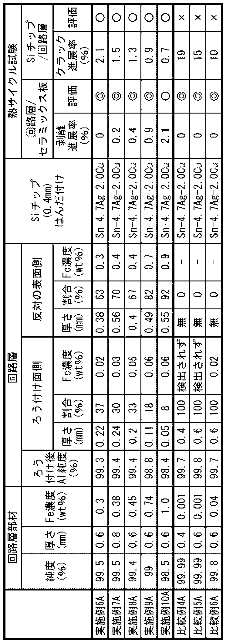
[0060] この結果、セラミックス板 11を Al Oとした場合であっても、回路層 12が、その全体の
2 3
平均純度が 98. 0wt%以上 99. 9wt%以下の A1合金により形成されるとともに、セラ ミックス板 11とのろう付け面 12a側に含まれる Feの濃度が 0. lwt%未満とされ、かつ このろう付け面 12aと反対の表面 12b側に含まれる Feの濃度が 0. lwt%以上とされ ていれば、前記の温度サイクルを 2000サイクル付与しても、剥離進展率およびクラッ ク進展率の双方が抑えられることが確認された。
[0061] さらに、上記のパワー素子搭載用基板 14においてセラミックス板 11を Si Nとしたも
3 4 のを形成して検証試験を実施した。評価結果を表 3に示す。
[0062] [表 3]

[0063] この結果、セラミックス板 11を Si Nとした場合であっても、回路層 12が、その全体の
3 4
平均純度が 98. Owt%以上 99. 9wt%以下の A1合金により形成されるとともに、セラ ミックス板 11とのろう付け面 12a側に含まれる Feの濃度が 0. lwt%未満とされ、かつ このろう付け面 12aと反対の表面 12b側に含まれる Feの濃度が 0. lwt%以上とされ
ていれば、前記の温度サイクルを 2000サイクル付与しても、剥離進展率およびクラッ ク進展率の双方が抑えられることが確認された。
[0064] 図 4はこの発明の一実施形態に係るパワー素子搭載用ユニットを適用したパワーモ ジュールを示す全体図である。
このパワーモジュール 110は、セラミックス板 111にお!/、てその表面に回路層 112 力 Sろう付けされるとともに、裏面に内部に冷却水路 113aが形成された冷却器 113が ろう付けされたパワー素子搭載用ユニット 114と、回路層 112の表面にはんだ層 115 を介してはんだ接合されたパワー素子 116とを備えている。
[0065] これらの各部材を形成する材質としては、例えば、セラミックス板 111では A1N、 Al
2
O、 Si N、 SiC等が挙げられ、冷却器 113では純 Al若しくは Al合金等が挙げられ、
3 3 4
はんだ層 115では例えば Sn— Ag— Cu系等の無鉛系のはんだ材が挙げられる。ま た、セラミックス板 111と回路層 112および冷却器 113とをろう付けするろう材では、 例えば Al— Si系等の A1系のろう材が挙げられる。本実施形態では、 Siを、 11. 6wt %以下で、かつ回路層 112を形成する後述の回路層部材に含まれる Siの濃度より高 い濃度含有する Al— Si系のろう材とされている。なお、冷却器 113は、その全体が純 A1若しくは A1合金等により一体的に形成されており、例えば铸造若しくは押出し成形 により形成することができる。
[0066] そして、本実施形態では、回路層 112は、全体の平均純度が 98. Owt%以上 99.
9wt%以下の A1合金により形成されるとともに、セラミックス板 111とのろう付け面 112 a側に含まれる Feの濃度が 0. lwt%未満で、かっこのろう付け面 112aと反対の表 面 112b側に含まれる Feの濃度が 0. ^%以上とされている。また、ろう付け面 112 a側は、回路層 112においてこのろう付け面 112aから前記反対の表面 112bに向け て回路層 112の厚さの 10%以上 50%以下までに位置する部分とされ、残部が前記 反対の表面 112b側とされて 、る。
[0067] 回路層 112に含まれる Feの濃度は、電子線マイクロアナライザ (EPMA)装置にお いて加速電圧を 15kVとし、かつ電流値を 5 X 10_8Aとして、スポットサイズを 30 μ m に設定し、回路層 112にお 、てろう付け面 112a側および前記反対の表面 112b側 についてそれぞれ、任意の 10箇所で測定し、得られた測定値の平均値を算出した。
また、回路層 112全体の平均純度は、まず、回路層 112を、水、フッ化水素酸およ び硝酸がそれぞれ同量ずつ混入された水浴中(約 100°C)に浸して分解し、その後、 この分解した試料を、 ICP— AES法 (誘導結合プラズマ—発光分析法)を用いること により測定した。
[0068] 次に、以上のように構成されたパワー素子搭載用ユニット 114の製造方法にっ 、て 説明する。
まず、回路層 112と同形同大の回路層部材を形成する。回路層部材は、その全体 の平均で、 Feを 0. 05wt%以上 1. Owt%以下含有する純度が 98. 5wt%以上 99. 95wt%以下の A1合金力もなつている。その後、セラミックス板 111の表面にろう材箔 と回路層部材とをこの順に配置する。また、セラミックス板 111の裏面にろう材箔を介 して冷却器 113を配置する。
以上より、セラミックス板 111において、その表面にろう材箔と回路層部材とがこの 順に配置され、裏面に前記ろう材箔と冷却器 113とがこの順に配置された積層体を 形成する。
[0069] そして、この積層体を、不活性雰囲気、還元雰囲気、または真空中(真空度 1 X 10 "5Torr (l. 33 X 10_3Pa)以下)【こ置! /、て、積層方向【こ 0. 098MPa〜0. 294MPa で加圧した状態で、 577°C以上 660°C以下で加熱し、ろう材箔を溶融させることによ つて、セラミックス板 111の表面に回路層部材をろう付けにより接合して回路層 112を 形成し、セラミックス板 111の裏面と冷却器 113とをろう付けにより接合してパワー素 子搭載用ユニット 114を形成する。
[0070] 以上説明したように、本実施形態によるパワー素子搭載用ユニット 114によれば、 回路層 112において、前記反対の表面 112b側に含まれる Feの濃度が 0.:^^%以 上とされて 、るので、この回路層 112全体の曲げ剛性を高めて冷却器 113の曲げ剛 性との差を縮めることが可能になり、このパワー素子搭載用ユニット 114を形成する 際のろう付け時に生ずる反り量を低減することができ、セラミックス板 111にクラックが 生じ易くなる等熱サイクル信頼性が低下するのを抑制することができる。
[0071] 一方、回路層 112において、ろう付け面 112a側に含まれる Feの濃度が 0. lwt% 未満とされているので、熱サイクル時に、セラミックス板 111および回路層 112の各熱
膨張係数の差に起因して、これらの接合界面に応力が生じようとした場合においても
、回路層 112のろう付け面 112a側を塑性変形させることによりこの応力を吸収させる ことが可能になる。これにより、前記接合界面に作用する応力を抑えることが可能に なり、セラミックス板 111と回路層 112との接合信頼性を向上させることもできる。なお 、ろう付け面 112a側に含まれる Feの濃度が 0. 05wt%以下であれば、このような作 用効果が確実に奏効されることになる。
[0072] また、回路層部材とセラミックス板 111とをろう付けする際、前記積層体を積層方向 に加圧するので、セラミックス板 111の表面と回路層部材との接合界面に酸ィ匕膜が 形成されるのを防ぐことが可能になり、回路層部材においてセラミックス板 111とのろ う付け面側に含まれる Feを、前記接合界面で溶融しているろう材中に良好に溶解さ せることができる。したがって、回路層 112のろう付け面 112a側に含まれる Feの濃度 が 0. lwt%未満とされ、かっこのろう付け面 112aと反対の表面 112b側に含まれる F eの濃度が 0. 1 %以上とされたパワー素子搭載用ユニット 114を確実に形成する ことができる。
[0073] さらに、回路層部材とセラミックス板 111とを接合するろう材箔に含まれる Siの濃度 力 回路層部材に含まれる Siの濃度よりも高くなつているので、ろう付け時の加熱によ り回路層部材における Siの限界固溶量が増大することと相俟って、溶融したろう材に 含まれる Siを、回路層部材の内部に向けてろう付け面側力 拡散させることが可能に なり、回路層部材において、ろう付け面側に含まれる Siの濃度を、前記反対の表面 側よりも高めることができる。これにより、ろう付け面側における Feの限界固溶量が、 前記反対の表面側よりも小さくなるので、ろう付け面側に含まれる Feの濃度を前記反 対の表面側よりも低くすることが可能になる。したがって、前述のように、回路層部材 にお 、てセラミックス板 111とのろう付け面側に含まれる Feを、前記接合界面で溶融 しているろう材中に良好に溶解させることが可能になることと相俟って、前記のパワー 素子搭載用ユニット 114をより一層確実に形成することができる。
[0074] また、本実施形態では、冷却器 113の全体が純 A1若しくは A1合金等により一体的 に形成されているので、この冷却器 113の構造を複雑にすることなぐパワー素子搭 載用ユニット 114を形成することが可能になり、その製造コストの増大を抑えることが
できるとともに、このパワー素子搭載用ユニット 114を備えるパワーモジュール 110の 積層方向におけるトータル熱抵抗を確実に低減することができる。
[0075] なお、本発明の技術的範囲は前記実施の形態に限定されるものではなぐ本発明 の趣旨を逸脱しない範囲において種々の変更をカ卩えることが可能である。
例えば、回路層部材は、母材を打ち抜いて形成したり、あるいはいわゆるエツチン グ法により形成してもよい。また、前記実施形態では、はんだ層 115のはんだ材とし て、例えば Sn—Ag— Cu系等の無鉛系のはんだ材を示した力 これに限らず、 Pbを 含むはんだ材、例えば PbSn系のはんだ材を採用してもよ 、。
[0076] また、前記実施形態では、パワーモジュール 110として、回路層 112の表面にはん だ層 115を介してパワー素子 116が接合された構成を示した力 これに代えて、例え ば、図 5に示されるように、回路層 112とパワー素子 116との間に、純 Cu、 Cu合金、 Cu— Mo系合金、若しくは Cu—C等の複合材料力もなるヒートスプレッダ 117を設け てもよい。この場合、パワー素子 116で発生した熱を、積層方向に直交する面方向に 沿って拡散させつつ積層方向に伝導させることが可能になる。
[0077] 次に、この製造方法についての具体的な実施例について説明する。
まず、材質については、回路層部材および冷却器 113を、 Feを約 0. 3wt%含有す る純度が 99. 5wt%の A1合金、回路層 112とセラミックス板 111とを接合するろう材を Al— Si系(A1が 92. 5wt%、Siが 7. 5wt%)、セラミックス板 111を A1Nによりそれぞ れ形成した。厚さについては、回路層 112を約 0. 8mm、ろう材箔を約 30 /ζ πι、セラ ミックス板 111を約 0. 635mmとした。なお、回路層 112は平面視四角形とされ、縦 および横の寸法をそれぞれ、約 17mmとした。また、セラミックス板 111も平面視四角 形とされ、縦および横の寸法をそれぞれ、約 20mmとした。
[0078] さらに、冷却器 113は、全体の高さ、すなわちセラミックス板 111の裏面がろう付けさ れる表面と、この表面と反対側の裏面との距離 A1が約 2. 5mmとされるとともに、全 体の幅 B1が約 21. 25mmとされ、さらに、全体の長さ、すなわち冷却水路 113aが延 在する方向(図 4の紙面の奥行き方向)の大きさを約 60mmとした。また、平面視四角 形の各冷却水路 113aでは、冷却器 113の高さ方向の大きさ C1を約 1. 5mmにし、 冷却器 113の幅方向の大きさ D1を約 1. 25mmにした。そして、これらの各冷却水路
113aを、冷却器 113の表裏面力 それぞれ約 0. 5mm離した前記高さ方向中央部 に形成し、また、冷却器 113の幅方向で隣合う冷却水路 113a同士の距離 E1を約 1 mmとし 7こ。
そして、前記積層体を 600°C〜650°Cの真空中(真空度 1 X 10"5Torr (l. 33 X 1 0_3Pa)以下)に置いて、約 1時間、積層方向に 0. 098MPa〜0. 294MPaで加圧し て、パワー素子搭載用ユニット 114を形成した。
[0079] 以上により形成された回路層 112において、電子マイクロアナライザ (EPMA)を用 い、ろう付け面 112a側の領域と前記反対の表面 112b側の領域とを判定した。具体 的には、回路層 112を切断し、その断面のろう付け面 112aから反対の表面 112bに 向かって、加速電圧 15kV、電流値 5 X 10_8A、スポットサイズ 1 μ m、 1点測定時間 5秒、移動間隔 1 μ mの条件で EPMAの線分析を行った。その結果を図 6に示す。 この図により、ろう付け面 112a力ら反対の表面 112bに向力つて 0. 15mmまでの領 域(回路層 112の厚さの約 25%に相当)では Feの濃度が低くなつており、それより反 対の表面 112b側では Feの濃度が高 、領域になって 、ることが確認される。
そして、回路層 112のろう付け面 112a側、および反対の表面 112b側の各 Fe濃度 は、加速電圧 15kV、電流値 5 X 10_8A、スポットサイズ 30 μ mの条件で EPMAを用 いて、ろう付け面 112a側、および反対の表面 112b側のそれぞれについて、任意の 10箇所で測定し、その平均値を算出することによって求めた。
[0080] 次に、以上説明した作用効果についての検証試験を実施した。
回路層を形成する回路層部材において、 A1の純度、厚さおよび Feの濃度の少なく とも 1つを異ならせて 8種類のパワー素子搭載用ユニットを形成し、各パワー素子搭 載用ユニットの回路層において、ろう付け面側に含まれる Feの濃度、前記反対の表 面側に含まれる Feの濃度、ろう付け面側の厚さ、および前記反対の表面側の厚さの 少なくとも 1つを異ならせた。そして、これらのパワー素子搭載用ユニットそれぞれの 回路層の表面に、同一の性能を有する Siチップを Sn— Ag— Cu系の無鉛はんだで はんだ接合したものを、— 40°Cから 105°Cに約 3分間で昇温した後、 105°Cから— 4 0°Cに 10分間で降温する温度履歴を 1サイクルとした熱サイクルを 2000サイクル付 与した。
[0081] その後、各パワー素子搭載用ユニットを 5箇所、積層方向に切断し、それぞれの切 断面を研磨した後、この切断面を超音波映像装置(140MHzプローブ)を用いて撮 像し、この切断面において、セラミックス板および回路層の接合界面の全長および剥 離進展長さをそれぞれ測定した。そして、前記接合界面の全長に対する剥離進展長 さの比率、つまり剥離進展率の平均値を算出した。また、同様にして、前記切断面に お 、て、セラミックス板および冷却器の接合界面の全長と剥離進展長さとをそれぞれ 測定し、この接合界面における剥離進展率の平均値を算出した。
剥離進展率が 5%を超えたものを Xとし、 2%以上 5%以下のものを〇とし、さらに 2 %未満のものを◎として評価した。
なお、前記 8種類のパワー素子搭載用ユニットにそれぞれ Siチップをはんだ接合す る前に、予め、各パワー素子搭載用ユニットに生じている反り量を測定し、反り量が 1 00 μ m以上のものを X、 100 μ m未満のものを〇として評価した。
結果を表 4に示す。
[0082] [表 4]
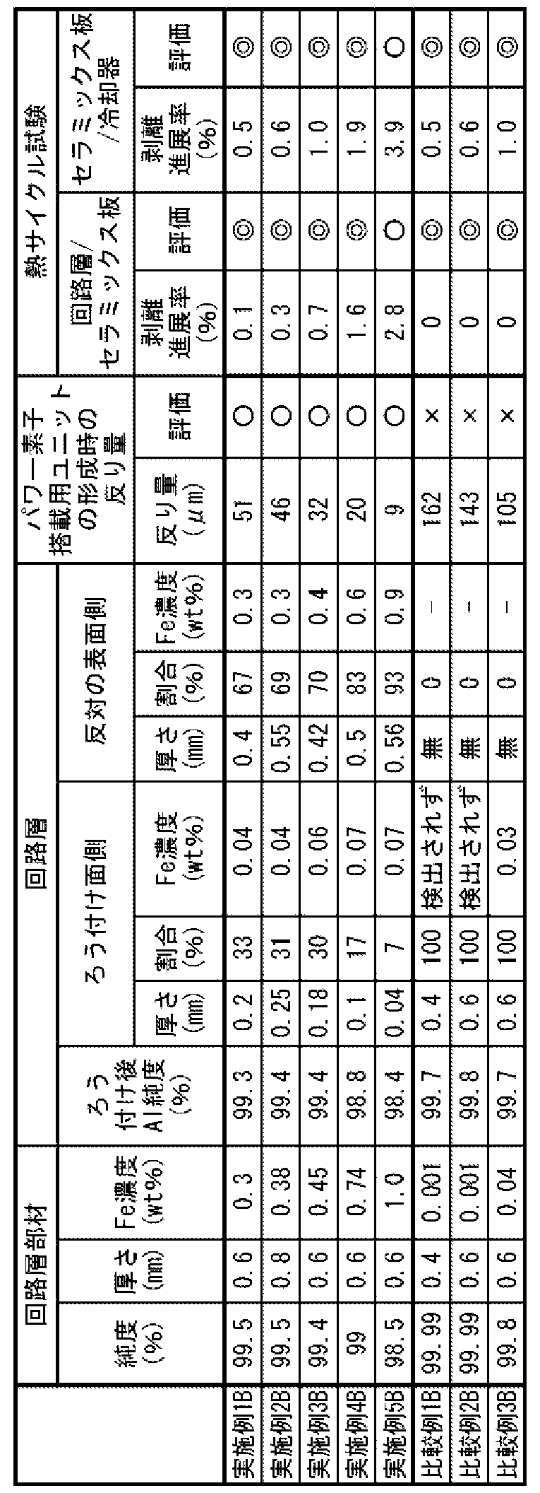
この結果、回路層 112が、その全体の平均純度が 98. Owt%以上 99. 9wt%以下 の A1合金により形成されるとともに、セラミックス板 111とのろう付け面 112a側に含ま れる Feの濃度が 0. lwt%未満とされ、かっこのろう付け面 112aと反対の表面 112b 側に含まれる Feの濃度が 0. lwt%以上とされていれば、パワー素子搭載用ユニット 114を形成する際のろう付け時に発生する反り量が抑えられ、し力も前記の温度サイ クルを 2000サイクル付与しても、前記各剥離進展率が抑えられ、前記の作用効果が 奏効されることが確認された。なお、表 4に記載はしていないが、実施例のパワーモ
ジュール 110では、前記温度サイクルを付与してもセラミックス板 111にクラックが発 生しなカゝつたことも確認された。
[0084] 図 7はこの発明の一実施形態に係るパワー素子搭載用ユニットを適用したパワーモ ジュールを示す全体図である。
このパワーモジュール 210は、セラミックス板 211にお!/、てその表面に回路層 212 力 Sろう付けされるとともに、裏面に冷却器 213がろう付けされたパワー素子搭載用ュ ニット 214と、回路層 212の表面にはんだ層 215を介してはんだ接合されたパワー素 子 216とを備えている。
[0085] これらの各部材を形成する材質としては、例えば、セラミックス板 211では A1N、 A1
2
O、 Si N若しくは SiC等が挙げられ、はんだ層 215では例えば Sn— Ag— Cu系等
3 3 4
の無鉛系のはんだ材、若しくは例えば PbSn系等の Pbを含むはんだ材が挙げられ、 回路層 212では純 A1若しくは A1合金が挙げられる。また、セラミックス板 211と回路 層 212および冷却器 213とをろう付けするろう材では、例えば Al— Si系等の A1系の ろう材が挙げられる。
[0086] そして、本実施形態では、冷却器 213は、セラミックス板 211とのろう付け面 218を 有する天板部 219と、この天板部 219においてろう付け面 218と反対の表面 220に 垂設された垂下部 221とを備えている。図示の例では、冷却器 213は、これらの天板 部 219および垂下部 221にカ卩えてさらに、前記反対の表面 220と対向する位置に天 板部 219と平行に配置された底板部 222を備えるとともに、垂下部 221は天板部 21 9と底板部 222とを連結し、かつ一定の方向に所定の間隔をあけて複数備えられ、こ の一定の方向と直交する方向に延在した壁部とされている。以上より、天板部 219の 反対の表面 220と底板部 222と複数の垂下部 221とで冷媒供給路 213aが複数画成 されて、冷却器 213は、その内部に複数の冷媒供給路 213aを有する、いわゆる多穴 管とされている。
[0087] さらに、これらの天板部 219、底板部 222および垂下部 221は、全体の平均純度が 98. Owt%以上 99. 9wt%以下の A1合金で一体的に形成されている。なお、冷却 器 213は例えば铸造若しくは押出し成形で形成される。そして、天板部 219において ろう付け面 218側の表層部 219aに含まれる Feの濃度が 0. lwt%未満とされ、かつ
この冷却器 213において表層部 219aを除いた部分に含まれる Feの濃度が 0. lwt %以上とされている。
図示の例では、ろう付け面 218はセラミックス板 211の裏面よりも大きぐセラミックス 板 211は、ろう付け面 218においてその外周縁よりも内方に位置する部分にろう付け されている。そして、前記表層部 219aは、ろう付け面 218においてセラミックス板 211 の裏面がろう付けされた部分に限定して形成されている。
[0088] ここで、冷却器 213に含まれる Feの濃度は、電子線マイクロアナライザ (EPMA)装 置において加速電圧を 15kVとし、かつ電流値を 5 X 10_8Aとして、スポットサイズを 30 μ mに設定し、冷却器 213において、表層部 219aおよび表層部 219aを除いた 部分についてそれぞれ、任意の 10箇所で測定し、得られた測定値の平均値を算出 して求めた。
また、冷却器 213全体の A1の平均純度は、まず、冷却器 213を、水、フッ化水素酸 および硝酸がそれぞれ同量ずつ混入された水浴中(約 100°C)に浸して分解し、そ の後、この分解した試料を、 ICP— AES法 (誘導結合プラズマ—発光分析法)を用い ること〖こより柳』定した。
[0089] 次に、以上のように構成されたパワー素子搭載用ユニット 214の製造方法について 説明する。
まず、セラミックス板 211の表面にろう材箔と回路層 212とをこの順に配置するととも に、セラミックス板 211の裏面にろう材箔と冷却器 213とをこの順に配置する。これに より、セラミックス板 211において、その表面にろう材箔と回路層 212とがこの順に配 置され、裏面にろう材箔と冷却器 213とがこの順に配置された積層体を形成する。セ ラミックス板 211と回路層 212との間に配置されたろう材箔の平面視形状は、回路層 212の平面視形状と略同形同大とされ、セラミックス板 211と冷却器 213との間に配 置されたろう材箔の平面視形状は、セラミックス板 211の平面視形状と略同形同大と されている。
[0090] そして、この積層体を、不活性雰囲気、還元雰囲気、または真空中(真空度 1 X 10 "5Torr (l. 33 X 10_3Pa)以下)【こ置! /、て、積層方向【こ 0. 098MPa〜0. 294MPa で加圧した状態で、 577°C以上 660°C以下で加熱し、ろう材箔を溶融させることによ
つて、セラミックス板 11の表面に回路層 12をろう付けにより接合し、セラミックス板 211 の裏面に冷却器 213をろう付けにより接合してパワー素子搭載用ユニット 214を形成 する。
[0091] 以上説明したように、本実施形態によるパワー素子搭載用ユニット 214によれば、 天板部 219においてろう付け面 218側の表層部 219aに含まれる Feの濃度が 0. lw t%未満とされているので、熱サイクル時使用に、セラミックス板 211および冷却器 21 3の各熱膨張係数の差に起因して、これらの接合界面に応力が生じようとした場合に おいても、表層部 219aを塑性変形させることによりこの応力を吸収させることが可能 になる。これにより、前記接合界面に発生する応力を抑えることが可能になり、セラミ ックス板 211と冷却器 213との接合信頼性を向上させることができる。
[0092] 一方、冷却器 213において表層部 219aを除いた部分に含まれる Feの濃度が 0. 1 wt%以上とされて、この表層部 219aを除いた部分の曲げ剛性は現行同等に維持す ることが可能になり、セラミックス板 211と冷却器 213とをろう付けするのに前記積層 体を積層方向に加圧したときに、この冷却器 213が薄肉に形成されて 、たとしても、 冷却器 213の垂下部 221が座屈するのを抑制することができる。
以上より、冷却器 213の垂下部 221の座屈強度を低下させることなぐパワーモジュ ール 210の熱サイクル信頼性を向上させることができる。なお、冷却器 213の表層部 219aに含まれる Feの濃度が 0. 05wt%以下であれば、このような作用効果が確実 に奏効されること〖こなる。
[0093] また、本実施形態では、冷却器 213の全体が前記 A1合金で一体的に形成されて いるので、この冷却器 213の構造を複雑にすることなぐパワー素子搭載用ユニット 2 14を形成することが可能になり、その製造コストの増大を抑えることができるとともに、 このパワー素子搭載用ユニット 214を備えるパワーモジュール 210の積層方向にお けるトータル熱抵抗を確実に低減することができる。
[0094] なお、本発明の技術的範囲は前記実施の形態に限定されるものではなぐ本発明 の趣旨を逸脱しない範囲において種々の変更をカ卩えることが可能である。
前記実施形態では、純 A1若しくは A1合金で形成された回路層 212を示した力 こ れに代えて、例えば純 Cu若しくは Cu合金で形成した回路層 212を採用してもょ 、。
また、前記実施形態では、冷却器 213として内部に複数の冷媒供給路 213aが形成 されたいわゆる多穴管を示した力 これに代えて、例えば、幅広の冷媒供給路が 1つ 形成された冷却器を採用してもよぐさらにこの幅広の冷媒供給路内において天板部 219の前記反対の表面 220にフィンをろう付けした冷却器を採用してもよい。また、こ れらに代えて、例えば、冷却器 213が、底板部 222を有さず天板部 219と垂下部 22 1とを備えて、天板部 219の前記反対の表面 220に、ピン若しくはフィンとしての垂下 部 221が複数垂設された冷却器を採用してもよい。
[0095] さらに、前記実施形態では、パワーモジュール 210として、回路層 212の表面には んだ層 215を介してパワー素子 216が接合された構成を示したが、これに代えて、例 えば、図 8に示されるように、回路層 212とパワー素子 216との間に、純 Cu、 Cu合金 、 Cu— Mo系合金、若しくは Cu—C等の複合材料力もなるヒートスプレッダ 217を設 けてもよい。この場合、パワー素子 216で発生した熱を、積層方向に直交する面方向 に沿って拡散させつつ積層方向に伝導させることが可能になる。
さらにまた、前記実施形態に代えて、セラミックス板 211の裏面とろう付け面 218とを 同形同大にして各々の外周縁を一致させた状態で、これら 211、 218をろう付けして もよい。この場合、表層部 219aはろう付け面 218の全域に形成されることになる。
[0096] 次に、この製造方法についての具体的な実施例について説明する。
まず、材質については、回路層 212および冷却器 213を、 Feを約 0. 3wt%含有す る純度が 99. 5wt%の A1合金、回路層 212とセラミックス板 211とを接合するろう材を Al— Si系(A1が 92. 5wt%、Siが 7. 5wt%)、セラミックス板 211を A1Nによりそれぞ れ形成した。厚さについては、回路層 212を約 0. 8mm、ろう材箔を約 30 /ζ πι、セラ ミックス板 211を約 0. 635mmとした。なお、回路層 212は平面視四角形とされ、縦 および横の寸法をそれぞれ、約 17mmとした。また、セラミックス板 211も平面視四角 形とされ、縦および横の寸法をそれぞれ、約 20mmとした。
[0097] さらに、冷却器 213は、全体の高さ、すなわちろう付け面 218と底板部 222の下面と の距離 A2が約 2. 5mmとされるとともに、全体の幅 B2が約 21. 25mmとされ、さらに 、全体の長さ、すなわち冷媒供給路 213aが延在する方向(図 7および図 8の紙面の 奥行き方向)の大きさを約 60mmとした。また、平面視四角形の各冷媒供給路 213a
では、冷却器 213の高さ方向の大きさ C2を約 1. 5mmにし、冷却器 213の幅方向の 大きさ D2を約 1. 25mmにした。そして、これらの各冷媒供給路 213aを、ろう付け面 218および底板部 222の下面力もそれぞれ約 0. 5mmずつ離した前記高さ方向中 央部に形成し、また、冷却器 213の幅方向で隣合う冷媒供給路 213a同士の距離 E2 を約 lmmとした。すなわち、天板部 219および底板部 222の各厚さを約 0. 5mmとし 、また、垂下部 221の厚さを約 lmmとした。
そして、前記積層体を 600°C〜650°Cの真空中(真空度 1 X 10"5Torr (l. 33 X 1 0_3Pa)以下)に置いて、約 1時間、積層方向に 0. 098MPa〜0. 294MPaで加圧し て、パワー素子搭載用ユニット 214を形成した。
[0098] 以上により形成された冷却器 213において、電子マイクロアナライザ (EPMA)を用 い、前記表層部 219aとそれ以外の部分とを判定した。本実施例では、冷却器 213を 切断し、その断面のろう付け面 218から冷媒供給路 213aの上面を構成する天板部 2 19の前記反対の表面 220まで、つまり天板部 219の厚さ方向全域 (約 0. 50mm)に ついて、加速電圧 15kV、電流値 5 X 10_8A、スポットサイズ 1 μ m、 1点測定時間 5 秒、移動間隔: mの条件で EPMAの線分析を行った。その結果を図 9に示す。 この図により、ろう付け面 218から前記反対の表面 220に向かって約 0. 10mmまで の領域では Feの濃度が低くなつており、天板部 219のうちこの領域より前記反対の 表面 220側の部分では Feの濃度が高くなつていることが確認される。
そして、冷却器 213において、表層部 219aおよびこの表層部 219a以外の部分の 各 Fe濃度は、加速電圧 15kV、電流値 5 X 10_8A、スポットサイズ 30 mの条件で E PMAを用いて、表層部 219aおよびこの表層部 219a以外の部分のそれぞれについ て、任意の 10箇所で測定し、その平均値を算出することによって求めた。
[0099] 次に、以上説明した作用効果についての検証試験を実施した。
冷却器を形成する A1合金の A1純度を異ならせた 6種類のパワー素子搭載用ュ-ッ トを形成し、これらのパワー素子搭載用ユニットの各冷却器において、前記表層部の 厚さ、表層部に含まれる Feの濃度、および冷却器において表層部以外の部分に含 まれる Feの濃度のうち少なくとも 1つを異ならせた。なお、実施例では、 A1純度を 98 . Owt%以上 99. 9wt%以下の範囲内で異ならせた 4種類の A1合金を用いて冷却
器を形成し、比較例では、 A1純度を 98. Owt%よりも小さい範囲で異ならせた 2種類 の A1合金を用いて冷却器を形成し、さらに、実施例および比較例の回路層は、 A1純 度が 99. 5wt%の A1合金を用いて形成した。また、前記各パワー素子搭載用ュ-ッ トを構成する各部材の寸法、セラミックス板の材質およびろう材の材質は前述した具 体的な実施例で示したものと同様にした。
そして、これらのパワー素子搭載用ユニットそれぞれの回路層の表面に、同一の性 能を有する Siチップを Sn—Ag— Cu系の無鉛はんだではんだ接合したものを、 -40 °Cから 125°Cに約 3分間で昇温した後、 125°Cから— 40°Cに 10分間で降温する温 度履歴を 1サイクルとした熱サイクルを 2000サイクル付与した。
[0100] その後、各パワー素子搭載用ユニットを 5箇所、積層方向に切断し、それぞれの切 断面を研磨した後、この切断面において、セラミックス板および冷却器の接合界面の 全長および剥離進展長さをそれぞれ測定した。そして、前記接合界面の全長に対す る剥離進展長さの比率、つまり剥離進展率の平均値を算出した。
結果を表 5に示す。
[0101] [表 5]

[0102] この結果、冷却器 213が、その全体の平均純度が 98. Owt%以上 99. 9wt%以下 の A1合金により形成されるとともに、表層部 219aに含まれる Feの濃度が 0. ^%未 満とされ、かっこの冷却器 213において表層部 219aを除いた部分に含まれる Feの 濃度が 0. ^%以上とされていれば、前記の温度サイクルを 2000サイクル付与して も、前記剥離進展率が抑えられ、前記の作用効果が奏効されることが確認された。な お、全体の平均純度が 99. 9wt%より大きい A1合金若しくは純 A1で形成した冷却器
をセラミックス板にろう付けしてパワー素子搭載用ユニットを形成しょうとしても前記垂 下部が座屈して形成することができないことも確認された。
[0103] 図 10はこの発明の一実施形態に係るパワー素子搭載用ユニットを適用したパワーモ ジュールを示す全体図である。
このパワーモジュール 310は、セラミックス板 311においてその表面に回路層 312 がろう付けされるとともに、裏面に内部に冷却水路 313aが形成された冷却器 313が ろう付けされたパワー素子搭載用ユニット 314と、回路層 312の表面にはんだ層 315 を介してはんだ接合されたパワー素子 316とを備えている。なお、冷却器 313は、回 路層 312の材質と同一の材質で形成されて 、る
[0104] これらの各部材を形成する材質としては、例えば、セラミックス板 311では A1N、 A1
2
O、 Si N、 SiC等が挙げられ、回路層 312および冷却器 313では純 A1若しくは A1
3 3 4
合金等が挙げられ、はんだ層 315では例えば Sn— Ag— Cu系等の無鉛系のはんだ 材が挙げられる。また、セラミックス板 311と回路層 312および冷却器 313とをろう付 けするろう材では、例えば Al— Si系等の A1系のろう材が挙げられる。
なお、冷却器 313は、その全体が純 A1若しくは A1合金等により一体的に形成されて おり、例えば铸造若しくは押出し成形により形成することができる。
[0105] そして、本実施形態では、回路層 312の厚さを A3、セラミックス板 311の厚さを B3 、冷却器 313にお 、てセラミックス板 311とのろう付け面 318を有する天板部 319の 厚さを C3としたときに、 0. 75 -B3< C3< l. 5 ·Α3く 3 ·Β3を満たしている。本実施 形態では、天板部 319の厚さ C3は、ろう付け面 318と冷却水路 313aの上面との距 離となっている。
[0106] 次に、以上のように構成されたパワー素子搭載用ユニット 314の製造方法について 説明する。
まず、セラミックス板 311の表面にろう材箔と回路層 312とをこの順に配置するととも に、セラミックス板 311の裏面にろう材箔を介して冷却器 313を配置する。
以上より、セラミックス板 311において、その表面にろう材箔と回路層 312とがこの順 に配置され、裏面に前記ろう材箔と冷却器 313とがこの順に配置された積層体を形 成する。
[0107] そして、この積層体を、不活性雰囲気、還元雰囲気、または真空中(真空度 1 X 10 "5Torr (l. 33 X 10_3Pa)以下)【こ置! /、て、積層方向【こ 0. 098MPa〜0. 294MPa で加圧した状態で、 577°C以上 660°C以下で加熱し、ろう材箔を溶融させることによ つて、セラミックス板 311の表面に回路層 312をろう付けにより接合し、セラミックス板 3 11の裏面に冷却器 313をろう付けにより接合してパワー素子搭載用ユニット 314を 形成する。
[0108] 以上説明したように、本実施形態によるパワー素子搭載用ユニット 314によれば、 回路層 312の厚さを A3、セラミックス板 311の厚さを B3、冷却器 313の天板部 319 の厚さを C3としたときに、 C3く 1. 5 · A3を満たしているので、冷却器 313の曲げ剛 性と、回路層 312の曲げ剛性との差を縮めて、パワー素子搭載用ユニット 314を形成 する際のろう付け時に生ずる反り量を低減することが可能になり、パワーモジュール 3 10にお 、て回路層 312の表面にパワー素子 316を接合するはんだ層 315にクラック が生ずるのを抑えることが可能になる。
[0109] また、 1. 5 ·Α3く 3 ·Β3を満たしているので、パワーモジュール 310の熱サイクル使 用時における回路層 312表面の面方向に沿った伸縮変形を、セラミックス板 311によ つて拘束することが可能になり、はんだ層 315にクラックが生じたとしてもその進展を 抑えることができる。さらに、 0. 75 'B3< C3を満たしているので、冷却器 313の曲げ 剛性と回路層 312の曲げ剛性との差を縮めたことに起因して冷却器 313の天板部 3 19が変形し易くなるのを抑えることが可能になり、このパワー素子搭載用ユニット 314 の使用が妨げられるのを防ぐことができる。
[0110] また、本実施形態では、冷却器 313の全体が純 A1若しくは A1合金等により一体的 に形成されているので、この冷却器 313の構造を複雑にすることなぐパワー素子搭 載用ユニット 314を形成することが可能になり、その製造コストの増大を抑えることが できる。
[0111] なお、本発明の技術的範囲は前記実施の形態に限定されるものではなぐ本発明 の趣旨を逸脱しない範囲において種々の変更をカ卩えることが可能である。
例えば、前記実施形態では、パワーモジュール 310として、回路層 312の表面には んだ層 315を介してパワー素子 316が接合された構成を示した力 これに代えて、例
えば、図 11に示されるように、回路層 312とパワー素子 316との間に、純 Cu、 Cu合 金、 Cu— Mo系合金、若しくは Cu—C等の複合材料力もなるヒートスプレッダ 317を 設けてもよい。この場合、パワー素子 316で発生した熱を、積層方向に直交する面方 向に沿って拡散させつつ積層方向に伝導させることが可能になる。
[0112] 次に、この製造方法についての具体的な実施例について説明する。
まず、材質については、回路層 312および冷却器 313を、純度が 99. 5wt%の A1 合金、回路層 312および冷却器 313とセラミックス板 311とを接合するろう材を A1 - S i系(A1が 92. 5wt%、Siが 7. 5wt%)、セラミックス板 311を A1Nによりそれぞれ形成 した。厚さについては、回路層 312の厚さ A3を約 400 m、 600 mまたは 800 m 、ろう材箱を約 30 μ m、セラミックス板 311の厚さ B3を約 500 μ mまたは約 635 μ m とした。なお、回路層 312は平面視四角形とされ、縦および横の寸法をそれぞれ、約 17mmとした。また、セラミックス板 311も平面視四角形とされ、縦および横の寸法を それぞれ、約 20mmとした。
[0113] さらに、冷却器 313は、全体の高さ、すなわち天板部 319のろう付け面 318と、この ろう付け面 318と反対側の裏面との距離 D3を約 2. 5mmとするととも〖こ、全体の幅 E 3を約 21. 25mmとし、さらに、全体の長さ、すなわち冷却水路 313aが延在する方向 (図 10の紙面の奥行き方向)の大きさを約 60mmとした。
また、平面視四角形の各冷却水路 313aは、冷却器 313においてろう付け面 318お よび前記裏面力 それぞれ同等の距離ずつ離した前記高さ方向中央部に形成して 天板部 319の厚さ C3を約 500 mとし、また、冷却器 313の幅方向で隣合う冷却水 路 313a同士の距離 F3を約 lmmとした。
そして、前記積層体を 600°C〜650°Cの真空中(真空度 1 X 10"5Torr (l. 33 X 1 0_3Pa)以下)に置いて、約 1時間、積層方向に 0. 098MPa〜0. 294MPaで加圧し て、パワー素子搭載用ユニット 314を形成した。
[0114] 次に、以上説明した作用効果についての検証試験を実施した。
回路層、セラミックス板、および冷却器の天板部それぞれの厚さのうち、少なくとも 1 つを異ならせ、他の部分は前述した具体的な実施例と同様にして 6種類のパワー素 子搭載用ユニットを形成した。そして、これらのパワー素子搭載用ユニットそれぞれの
回路層の表面に、同一の性能を有する Siチップを Sn— Ag— Cu系の無鉛はんだで はんだ接合したものを、— 40°Cから 105°Cに約 3分間で昇温した後、 105°Cから— 4 0°Cに 10分間で降温する温度履歴を 1サイクルとした熱サイクルを 2000サイクル付 与した。
[0115] その後、各パワー素子搭載用ユニットを 5箇所、積層方向に切断し、それぞれの切 断面を研磨した後、この切断面を光学顕微鏡を用いて撮像し、この切断面において 、回路層と Siチップとをはんだ接合するはんだ層の全長、およびこのはんだ層で発 生したクラック進展長さをそれぞれ測定した。そして、はんだ層の全長に対するクラッ ク進展長さの比率、つまりクラック進展率の平均値を算出した。
なお、前記 6種類のパワー素子搭載用ユニットにそれぞれ Siチップをはんだ接合す る前に、予め、各パワー素子搭載用ユニットに生じている反り量を測定した。
結果を表 6に示す。
[0116] [表 6]

[0117] この結果、回路層 12の厚さ A3、セラミックス板 11の厚さ B3、および冷却器 13の天 板部 19の厚さ C3の関係が、 0. 75 -B3< C3< l. 5 ·Α3く 3 ·Β3を満たしていれば、 ノ^ー素子搭載用ユニット 14を形成する際のろう付け時に発生する反り量が抑えら れ、し力も前記の温度サイクルを 2000サイクル付与しても、前記クラック進展率が抑 えられ、前記の作用効果が奏効されることが確認された。なお、表 6に記載はしてい ないが、実施例のパワーモジュール 310では、前記温度サイクルを付与してもセラミ ックス板 311にクラックが発生しなカゝつたことも確認された。
[0118] 図 12はこの発明の一実施形態に係るパワー素子搭載用基板を適用したパワーモジ ユールを示す全体図である。
このパワーモジュール 410は、セラミックス板 411の表面に回路層 412がろう付けさ れるとともに、この回路層 412の表面 412bに純 Cu若しくは Cu合金からなるヒートブ ロック 413が第 1はんだ層 414を介してはんだ接合されたパワー素子搭載用基板 41 5と、ヒートブロック 413の表面に第 2はんだ層 416を介してはんだ接合された半導体 チップ (パワー素子) 417とを備えて 、る。
[0119] 本実施形態では、パワー素子搭載用基板 415は、さらにセラミックス板 411の裏面 にろう付けされた冷却器 418を備えている。なお、図示の例では、冷却器 418は、そ の内部に複数の冷媒供給路 418aを有する、いわゆる多穴管とされている。また、ヒ ートブロック 413は、純度が 50wt%以上の Cu合金若しくは純 Cuで形成されている。
[0120] これらの各部材を形成する材質としては、例えば、セラミックス板 411では A1N、 A1
2
O、 Si N若しくは SiC等が挙げられ、第 1、第 2はんだ層 414、 416では例えば Sn
3 3 4
Ag— Cu系等の無鉛系のはんだ材、若しくは例えば PbSn系等の Pbを含むはんだ 材が挙げられ、冷却器 418では純 A1若しくは A1合金が挙げられる。また、セラミックス 板 411と回路層 412および冷却器 418とをろう付けするろう材では、例えば Al— Si系 等の A1系のろう材が挙げられる。本実施形態では、このろう材は、 Siを、 11. 6wt% 以下で、かつ回路層 412を形成する後述の回路層部材に含まれる Siの濃度より高い 濃度含有している。
[0121] そして、本実施形態では、回路層 412は、全体の平均純度が 98. Owt%以上 99.
9wt%以下の A1合金で形成されるとともに、ヒートブロック 413がはんだ接合された表 面 412b側に含まれる Feの濃度が 0. ^%以上とされ、かつセラミックス板 411がろ う付けされた裏面 412a側に含まれる Feの濃度が 0. lwt%未満となっている。
[0122] また、回路層 412の厚さは 0. 4mm以上とされるとともに、回路層 412の裏面 412a 側は、回路層 412において、この裏面 412aから前記表面 412bに向けて 0. 04mm 以上かつ回路層 412の厚さの半分以下までに位置する部分とされ、残部が回路層 4 12の表面 412b側となっている。なお、前記裏面 412a側に含まれる Feの濃度は、セ ラミックス板 411と回路層 412の裏面 412aとの接合界面における剥離進展率低減の 観点から 0. 05wt%以下であることが好まし 、。
[0123] 回路層 412において前記裏面 412a側、および表面 412b側の特定は、回路層 41
2を切断して得られた断面にぉ ヽて、電子マイクロアナライザ (EPMA)装置を用い、 裏面 412a力ら表面 412bに向力つて、加速電圧 15kV、電流値 5 X 10_8A、スポット サイズ 1 μ m、 1点測定時間 5秒、移動間隔 1 μ mの条件で EPMAの線分析を行い、 得られたデータから、 Feの濃度が 0. lwt%以上である領域と、 0. lwt%未満である 領域との境界を特定することにより行った。
そして、このようにして特定された前記裏面 412a側および前記表面 412b側それぞ れについて、 EPMA装置において加速電圧を 15kVとし、かつ電流値を 5 X 10_8A として、スポットサイズを 30 mに設定し、前記断面における任意の 10箇所で測定し 、得られた測定値の平均値を算出することにより、前記裏面 412a側および前記表面 412b側それぞれに含まれる Feの濃度を求めた。
また、回路層 412全体の平均純度は、まず、回路層 412を、水、フッ化水素酸およ び硝酸がそれぞれ同量ずつ混入された水浴中(約 100°C)に浸して分解し、その後、 この分解した試料を、 ICP— AES法 (誘導結合プラズマ—発光分析法)を用いること により測定した。
[0124] 次に、以上のように構成されたパワー素子搭載用基板 415の製造方法について説 明する。
まず、回路層 412と同形同大の回路層部材を形成する。回路層部材は、その全体 の平均で、 Feを 0. 05wt%以上 1. Owt%以下含有する純度が 98. 5wt%以上 99. 95wt%以下の A1合金からなっている。その後、セラミックス板 411の表面にろう材箔 と回路層部材とをこの順に配置する。また、セラミックス板 411の裏面にろう材箔を介 して冷却器 418を配置する。
以上より、セラミックス板 411において、その表面にろう材箔と回路層部材とがこの 順に配置され、裏面に前記ろう材箔と冷却器 418とがこの順に配置された積層体を 形成する。
[0125] そして、この積層体を、不活性雰囲気、還元雰囲気、または真空中(真空度 1 X 10 "5Torr (l. 33 X 10_3Pa)以下)【こ置! /、て、積層方向【こ 0. 098MPa〜0. 294MPa で加圧した状態で、 577°C以上 660°C以下で加熱し、ろう材箔を溶融させることによ つて、セラミックス板 411の表面に回路層部材をろう付けして回路層 412を形成すると
ともに、セラミックス板 411の裏面に冷却器 418をろう付けする。
その後、回路層 412の表面 412bにヒートブロック 413を第 1はんだ層 414を介して はんだ接合することにより、パワー素子搭載用基板 415を形成する。
[0126] 以上説明したように、本実施形態によるパワー素子搭載用基板 415によれば、回路 層 412の裏面 412a側に含まれる Feの濃度が 0. lwt%未満となっているので、熱サ イタル使用時に、セラミックス板 411および回路層 412の各熱膨張係数の差に起因し て、これらの接合界面に応力が生じようとした場合においても、回路層 412の裏面 41 2a側を塑性変形させることによりこの応力を吸収させることが可能になる。これにより 、前記接合界面に作用する応力を抑えることが可能になり、熱サイクル使用時におけ るセラミックス板 411と回路層 412との接合信頼性を向上させることができる。
[0127] 一方、回路層 412の表面 412b側に含まれる Feの濃度が 0. 1 %以上となってい るので、熱サイクル使用時に回路層 412が繰り返し熱変形するのに伴い、徐々にこの 表面 412b側を硬化させることが可能になり、この部分に発生する塑性変形量を抑え ることができる。これにより、回路層 412の表面 412bとヒートブロック 413とを接合する 第 1はんだ層 414に作用する、熱サイクル使用時の回路層 412の塑性変形に起因し た負荷を低減することが可能になり、熱サイクル使用時に、この第 1はんだ層 414にク ラックが発生してもその進展を抑えることができる。
[0128] また、回路層 412と半導体チップ 417との間にヒートブロック 413が介在しているの で、半導体チップ 417から第 2はんだ層 416を介してヒートブロック 413に伝導した熱 を即座にその沿面方向に分散させることが可能になり、熱サイクル使用時に、この半 導体チップ 417の温度が上昇するのを抑えることができる。
[0129] さらに、本実施形態では、回路層 412の厚さは 0. 4mm以上とされるとともに、回路 層 412の裏面 412a側は、回路層 412において、この裏面 412aから前記表面 412b に向けて 0. 04mm以上かつ回路層 412の厚さの半分以下までに位置する部分とさ れ、残部が回路層 412の表面 412b側となっているので、前記の作用効果が確実に 奏効されることになる。また、回路層 412の厚さが 0. 4mm以上となっているので、パ ヮーモジュール 410の一般的な要求仕様を確実に満たすことができる。
[0130] また、本実施形態によるパワー素子搭載用基板の製造方法によれば、回路層部材
とセラミックス板 411とをろう付けする際、前記積層体を積層方向に加圧するので、セ ラミックス板 411の表面と回路層部材との接合界面に酸ィ匕膜が形成されるのを防ぐこ とが可能になり、回路層部材においてセラミックス板 411とのろう付け面側に含まれる Feを、前記接合界面で溶融しているろう材中に良好に溶解させることができる。した がって、回路層 412の表面 412b側に含まれる Feの濃度が 0. ^%以上とされ、力 つ回路層 412の裏面 412a側に含まれる Feの濃度が 0. lwt%未満とされたパワー 素子搭載用基板 415を確実に形成することができる。
[0131] さらに、回路層部材とセラミックス板 411とを接合するろう材箔に含まれる Siの濃度 力 回路層部材に含まれる Siの濃度よりも高くなつているので、ろう付け時の加熱によ り回路層部材における Siの限界固溶量が増大することと相俟って、溶融したろう材に 含まれる Siを、回路層部材の内部に向けて前記ろう付け面側力 拡散させることが可 能になり、回路層部材において、前記ろう付け面側に含まれる Siの濃度を、このろう 付け面と反対の表面側よりも高めることができる。これにより、前記ろう付け面側にお ける Feの限界固溶量が、前記表面側よりも小さくなるので、このろう付け面側に含ま れる Feの濃度を前記表面側よりも低くすることが可能になる。したがって、前述のよう に、回路層部材においてセラミックス板 411とのろう付け面側に含まれる Feを、前記 接合界面で溶融しているろう材中に良好に溶解させることが可能になることと相俟っ て、前記のパワー素子搭載用基板 415をより一層確実に形成することができる。
[0132] なお、本発明の技術的範囲は前記実施の形態に限定されるものではなぐ本発明 の趣旨を逸脱しない範囲において種々の変更をカ卩えることが可能である。
例えば、回路層部材は、母材を打ち抜いて形成したり、あるいはいわゆるエツチン グ法により形成してもよい。
また、前記実施形態では、パワー素子搭載用基板 415の冷却器 418として、その 内部に複数の冷媒供給路 418aを有する、いわゆる多穴管を示した力 これに代えて 、例えば、冷媒供給路 418aを形成しなくてもよいし、あるいは冷媒供給路 418aを 1 つだけ形成してもよいし、さらには冷媒供給路 418aの内面に冷却フィンを設けてもよ い。さらにまた、パワー素子搭載用基板に冷却器 418を設けなくてもよい。
[0133] 次に、この製造方法についての具体的な実施例について説明する。
まず、材質については、回路層部材および冷却器 418を、 Feを約 0. 3wt%含有す る純度が 99. 5wt%の A1合金、ヒートブロック 413を純度が 99. 99wt%の OFC (無 酸素銅)、回路層部材および冷却器 418とセラミックス板 411とを接合するろう材を A1 — Si系(A1が 92. 5wt%、 Siが 7. 5wt%)、第 1はんだ層 414を Sn—Ag— Cu系、セ ラミックス板 411を A1Nでそれぞれ形成した。
厚さについては、回路層部材(回路層 412)を 0. 6mm,ろう材箔を約 30 m、セラ ミックス板 411を 0. 635mm,ヒートブロック 413を 1. 5mmとした。なお、回路層部材 (回路層 412)は平面視四角形とされ、縦および横の寸法をそれぞれ、 17mmおよび 36mmとした。また、セラミックス板 411も平面視四角形とされ、縦および横の寸法を それぞれ、 20mmおよび 40mmとした。さらに、ヒートブロック 413も平面視四角形と され、縦および横の寸法をそれぞれ、 15mmおよび 30mmとした。
[0134] さらに、冷却器 418は、全体の高さが 2. 5mmとされるとともに、全体の幅が 22mm とされ、さらに、全体の長さ、すなわち冷媒供給路 418aが延在する方向(図 12の紙 面の奥行き方向)の大きさを 50mmとした。また、正面視四角形の各冷媒供給路 418 aでは、冷却器 418の高さ方向の大きさを 1. 5mmにし、冷却器 418の幅方向の大き さを 1. 25mmにした。
そして、前記積層体を 600°C〜650°Cの真空中(真空度 1 X 10"5Torr (l. 33 X 1 0_3Pa)以下)に置いて、約 1時間、積層方向に 0. 098MPa〜0. 294MPaで加圧し 、セラミックス板 411の表面に回路層部材をろう付けして回路層 412を形成するととも に、セラミックス板 411の裏面に冷却器 418をろう付けした。
その後、回路層 412の表面 412bに第 1はんだ層 414を介してヒートブロック 413を 接合してパワー素子搭載用基板 415を形成した。
[0135] このパワー素子搭載用基板 415の回路層 412に対して、電子マイクロアナライザ (E PMA)を用い、その裏面 412a側の領域と前記表面 412b側の領域とを判定した。具 体的には、回路層 412を切断して得られた断面において、裏面 412aから表面 412b に向かって、加速電圧 15kV、電流値 5 X 10_8A、スポットサイズ 1 μ m、 1点測定時 間 5秒、移動間隔 1 μ mの条件で ΕΡΜΑの線分析を行った。その結果を図 13に示 す。
この図より、回路層 412においてその裏面 412aから表面 412bに向かって 0. 15m mまでの領域(回路層 412の厚さの約 25%に相当)では Feの濃度が 0. lwt%未満 で低くなつており、それより表面 412b側では Feの濃度が 0. ^%以上で高くなつて いることが確認される。
[0136] 次に、以上説明した作用効果についての検証試験を実施した。
回路層を形成する回路層部材において、 A1の純度、厚さおよび Feの濃度のうち少 なくとも 1つを異ならせて 7種類のパワー素子搭載用基板を形成し、各パワー素子搭 載用基板の回路層にお 、て、セラミックス板がろう付けされた裏面側に含まれる Feの 濃度、ヒートブロックがはんだ接合された表面側に含まれる Feの濃度、前記裏面側の 厚さ、および前記表面側の厚さのうち少なくとも 1つを異ならせた。そして、これらのパ ヮー素子搭載用基板それぞれのヒートブロックの表面に、同一の性能を有する半導 体チップを Sn— Ag - Cu系の無鉛はんだではんだ接合したものを、— 40°Cから 105 °Cに約 3分間で昇温した後、 105°Cから— 40°Cに約 10分間で降温する温度履歴を 1サイクルとした熱サイクルを 2000サイクル付与した。
[0137] その後、各パワー素子搭載用基板を超音波映像装置(140MHzプローブ)で撮像 し、得られた撮像データに基づいて、セラミックス板と回路層の裏面との接合界面の 面積に対する剥離進展面積の比率、つまり剥離進展率を算出した。
また、前記撮像データに基づいて、回路層の表面とヒートブロックとを接合する第 1 はんだ層の横断面積に対するクラック進展面積の比率、つまりクラック進展率を算出 した。
さらに、前記撮像データに基づいて、ヒートブロックと半導体チップとを接合する第 2 はんだ層の横断面積に対するクラック進展面積の比率、つまりクラック進展率を算出 した。
結果を表 7に示す。
[0138] [表 7]
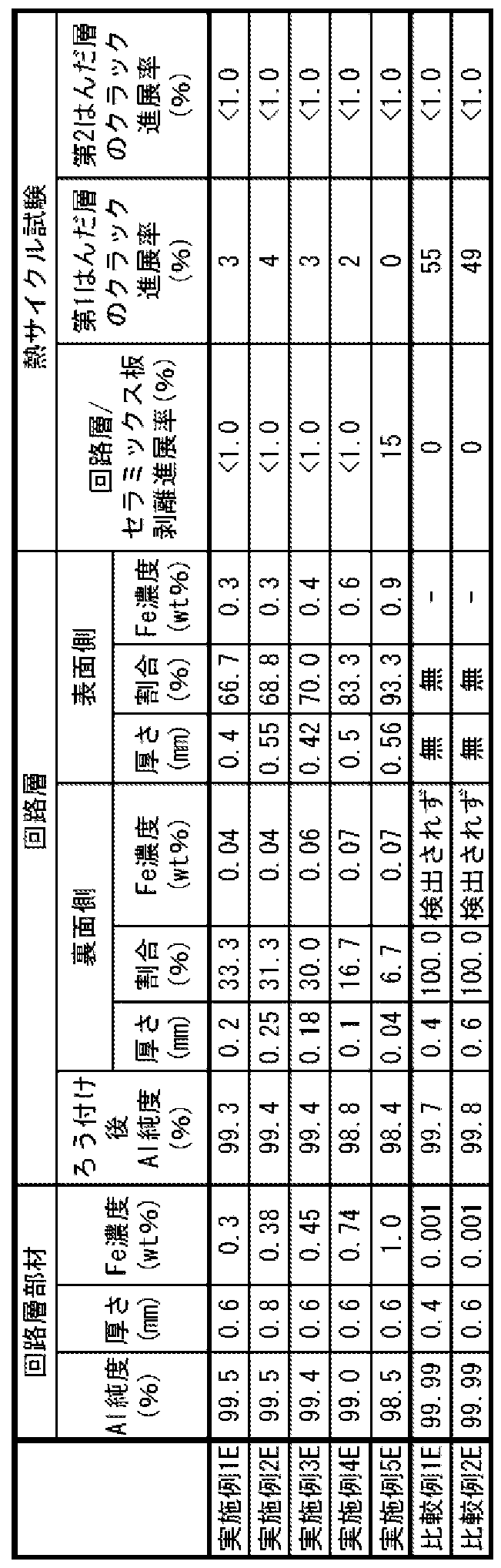
この結果、回路層 412が、その全体の平均純度が 98. Owt%以上 99. 9wt%以下 の A1合金で形成されるとともに、ヒートブロック 413がはんだ接合された表面 412b側 に含まれる Feの濃度が 0. 1 %以上とされ、かつセラミックス板 411がろう付けされ た裏面 412a側に含まれる Feの濃度が 0. lwt%未満となっていれば、前記の温度サ イタルを 2000サイクル付与しても、前述した剥離進展率およびクラック進展率の双方 が抑えられ、前記の作用効果が奏効されることが確認された。
産業上の利用可能性
[0140] 回路層とパワー素子とをはんだ接合するのに無鉛系のはんだ材を採用しても、熱 サイクル時にこのはんだ層でクラックが進展し易くなるのを抑えることができる。
[0141] また、セラミックス板の裏面に冷却器を直接ろう付けしても、パワー素子搭載用ュ- ットを形成した際の反りの発生を抑え、熱サイクル信頼性の低下を抑制することがで きる。
[0142] また、冷却器の垂下部の座屈強度を低下させることなぐパワーモジュールの熱サ イタル信頼性を向上させることができる。
[0143] また、パワーモジュールの熱サイクル使用時における接合信頼性を向上させること ができる。
Claims
[1] セラミックス板の表面に回路層がろう付けされてなり、この回路層の表面にパワー素 子がはんだ接合されるパワー素子搭載用基板であって、
前記回路層は、全体の平均純度が 98. Owt%以上 99. 9wt%以下の A1合金によ り形成されるとともに、前記セラミックス板とのろう付け面側に含まれる Feの濃度が 0. lwt%未満とされ、かっこのろう付け面と反対の表面側に含まれる Feの濃度が 0. 1 wt%以上とされていることを特徴とするパワー素子搭載用基板。
[2] 請求項 1記載のパワー素子搭載用基板において、
前記ろう付け面側は、回路層においてこのろう付け面力 前記反対の表面に向け て回路層の厚さの 10%以上 50%以下までに位置する部分とされ、残部が前記反対 の表面側とされていることを特徴とするパワー素子搭載用基板。
[3] セラミックス板の表面に回路層がろう付けされてなり、この回路層の表面にパワー素 子がはんだ接合されるパワー素子搭載用基板の製造方法であって、
セラミックス板の表面に、 A1系のろう材箔と、 Feを 0. 05wt%以上 1. Owt%以下含 有する純度が 98. 5wt%以上 99. 95wt%以下の A1合金力もなる回路層部材とをこ の順に配置して積層体とした後に、
この積層体を積層方向に加圧した状態で加熱し、ろう材箔を溶融させて、セラミック ス板の表面に回路層部材をろう付けすることにより、請求項 1または 2に記載のパワー 素子搭載用基板を形成することを特徴とするパワー素子搭載用基板の製造方法。
[4] セラミックス板の表面に回路層がろう付けされたパワー素子搭載用基板と、回路層 の表面にはんだ接合されたパワー素子とを備えたパワーモジュールであって、 前記パワー素子搭載用基板が請求項 1または 2に記載のパワー素子搭載用基板で あることを特徴とするパワーモジュール。
[5] セラミックス板においてその表面に回路層がろう付けされるとともに、裏面に内部に 冷却水路が形成された冷却器がろう付けされたパワー素子搭載用ユニットであって、 前記回路層は、全体の平均純度が 98. Owt%以上 99. 9wt%以下の A1合金によ り形成されるとともに、前記セラミックス板とのろう付け面側に含まれる Feの濃度が 0. lwt%未満とされ、かっこのろう付け面と反対の表面側に含まれる Feの濃度が 0. 1
wt%以上とされていることを特徴とするパワー素子搭載用ユニット。
[6] 請求項 5記載のパワー素子搭載用ユニットにおいて、
前記ろう付け面側は、回路層においてこのろう付け面力 前記反対の表面に向け て回路層の厚さの 10%以上 50%以下までに位置する部分とされ、残部が前記反対 の表面側とされていることを特徴とするパワー素子搭載用ユニット。
[7] セラミックス板においてその表面に回路層がろう付けされるとともに、裏面に内部に 冷却水路が形成された冷却器がろう付けされたパワー素子搭載用ユニットの製造方 法であって、
セラミックス板の表面に、 A1系のろう材箔と、 Feを 0. 05wt%以上 1. Owt%以下含 有する純度が 98. 5wt%以上 99. 95wt%以下の A1合金力もなる回路層部材とをこ の順に配置して積層体とした後に、
この積層体を積層方向に加圧した状態で加熱し、ろう材箔を溶融させて、セラミック ス板の表面に回路層部材をろう付けすることにより、請求項 5または 6に記載のパワー 素子搭載用ユニットを形成することを特徴とするパワー素子搭載用ユニットの製造方 法。
[8] セラミックス板においてその表面に回路層がろう付けされるとともに、裏面に内部に 冷却水路が形成された冷却器がろう付けされたパワー素子搭載用ユニットと、回路層 の表面にはんだ接合されたパワー素子とを備えたパワーモジュールであって、 前記パワー素子搭載用ユニットが請求項 5または 6に記載のパワー素子搭載用ュ ニットであることを特徴とするパワーモジュール。
[9] セラミックス板においてその表面に回路層がろう付けされるとともに、裏面に冷却器 力 Sろう付けされたパワー素子搭載用ユニットであって、
前記冷却器は、前記セラミックス板とのろう付け面を有する天板部と、この天板部に おいて前記ろう付け面と反対の表面に垂設された垂下部とを備えるとともに、全体の 平均純度が 98. Owt%以上 99. 9wt%以下の A1合金で形成され、
前記天板部にぉ 、てろう付け面側の表層部に含まれる Feの濃度が 0. lwt%未満 とされ、かっこの冷却器にお!、て前記表層部を除 、た部分に含まれる Feの濃度が 0 . lwt%以上とされていることを特徴とするパワー素子搭載用ユニット。
[10] セラミックス板においてその表面に回路層がろう付けされるとともに、裏面に冷却器 力 Sろう付けされたパワー素子搭載用ユニットの製造方法であって、
セラミックス板の裏面にろう材箔と冷却器とをこの順に配置して積層体とした後に、 この積層体を積層方向に加圧した状態で加熱し、ろう材箔を溶融させて、セラミック ス板の裏面に冷却器をろう付けすることにより、請求項 9記載のパワー素子搭載用ュ ニットを形成することを特徴とするパワー素子搭載用ユニットの製造方法。
[11] セラミックス板においてその表面に回路層がろう付けされるとともに、裏面に冷却器 力 Sろう付けされたパワー素子搭載用ユニットと、回路層の表面にはんだ接合されたパ ヮー素子とを備えたパワーモジュールであって、
前記パワー素子搭載用ユニットが請求項 9記載のパワー素子搭載用ユニットである ことを特徴とするパワーモジュール。
[12] セラミックス板においてその表面に回路層がろう付けされるとともに、裏面に前記回 路層の材質と同一の材質力もなる冷却器がろう付けされたパワー素子搭載用ユニット であって、
前記回路層の厚さを A3、セラミックス板の厚さを B3、前記冷却器において前記セ ラミックス板とのろう付け面を有する天板部の厚さを C3としたときに、 0. 75 -B3< C3 < 1. 5 ·Α3く 3 ·Β3を満たすことを特徴とするパワー素子搭載用ユニット。
[13] セラミックス板においてその表面に回路層がろう付けされるとともに、裏面に前記回 路層の材質と同一の材質力もなる冷却器がろう付けされたパワー素子搭載用ユニット と、回路層の表面にはんだ接合されたパワー素子とを備えたパワーモジュールであ つて、
前記パワー素子搭載用ユニットが請求項 12記載のパワー素子搭載用ユニットであ ることを特徴とするパワーモジュール。
[14] セラミックス板の表面に回路層がろう付けされるとともに、この回路層の表面に純 Cu 若しくは Cu合金力もなるヒートブロックがはんだ接合されてなり、このヒートブロックの 表面にパワー素子がはんだ接合されるパワー素子搭載用基板であって、
前記回路層は、全体の平均純度が 98. Owt%以上 99. 9wt%以下の A1合金で形 成されるとともに、前記ヒートブロックがはんだ接合された表面側に含まれる Feの濃度
が 0. lwt%以上とされ、かつ前記セラミックス板がろう付けされた裏面側に含まれる F eの濃度が 0. lwt%未満とされていることを特徴とするパワー素子搭載用基板。
[15] 請求項 14記載のパワー素子搭載用基板において、
前記回路層の厚さは 0. 4mm以上とされるとともに、前記回路層の裏面側は、回路 層において、この裏面から前記表面に向けて 0. 04mm以上かつ回路層の厚さの半 分以下までに位置する部分とされ、残部が前記回路層の表面側となっていることを特 徴とするパワー素子搭載用基板。
[16] セラミックス板の表面に回路層がろう付けされるとともに、この回路層の表面に純 Cu 若しくは Cu合金力もなるヒートブロックがはんだ接合されてなり、このヒートブロックの 表面にパワー素子がはんだ接合されるパワー素子搭載用基板の製造方法であって セラミックス板の表面に、 A1系のろう材箔と、 Feを 0. 05wt%以上 1. Owt%以下含 有する純度が 98. 5wt%以上 99. 95wt%以下の A1合金力もなる回路層部材とをこ の順に配置して積層体とした後に、
この積層体を積層方向に加圧した状態で加熱し、ろう材箔を溶融させて、セラミック ス板の表面に回路層部材をろう付けして前記回路層を形成し、
その後、前記回路層の表面に前記ヒートブロックをはんだ接合することにより、請求 項 14または 15に記載のパワー素子搭載用基板を形成することを特徴とするパワー 素子搭載用基板の製造方法。
[17] セラミックス板の表面に回路層がろう付けされるとともに、この回路層の表面に純 Cu 若しくは Cu合金カゝらなるヒートブロックがはんだ接合されたパワー素子搭載用基板と 、前記ヒートブロックの表面にはんだ接合されたパワー素子とを備えたパワーモジュ 一ノレであって、
前記パワー素子搭載用基板が請求項 14または 15に記載のパワー素子搭載用基 板であることを特徴とするパワーモジュール。
Priority Applications (1)
| Application Number | Priority Date | Filing Date | Title |
|---|---|---|---|
| US12/303,513 US8198540B2 (en) | 2006-06-06 | 2007-06-06 | Power element mounting substrate, method of manufacturing the same, power element mounting unit, method of manufacturing the same, and power module |
Applications Claiming Priority (12)
| Application Number | Priority Date | Filing Date | Title |
|---|---|---|---|
| JP2006157124 | 2006-06-06 | ||
| JP2006-157124 | 2006-06-06 | ||
| JP2006157125A JP4876719B2 (ja) | 2006-06-06 | 2006-06-06 | パワー素子搭載用ユニットおよびパワー素子搭載用ユニットの製造方法並びにパワーモジュール |
| JP2006-157125 | 2006-06-06 | ||
| JP2006-169838 | 2006-06-20 | ||
| JP2006169838A JP4882538B2 (ja) | 2006-06-20 | 2006-06-20 | パワー素子搭載用ユニットおよびパワー素子搭載用ユニットの製造方法並びにパワーモジュール |
| JP2006-191468 | 2006-07-12 | ||
| JP2006191468A JP4984696B2 (ja) | 2006-07-12 | 2006-07-12 | パワー素子搭載用ユニットおよびパワーモジュール |
| JP2006-224112 | 2006-08-21 | ||
| JP2006224112A JP4882596B2 (ja) | 2006-08-21 | 2006-08-21 | パワー素子搭載用基板およびパワー素子搭載用基板の製造方法並びにパワーモジュール |
| JP2007-061640 | 2007-03-12 | ||
| JP2007061640A JP4910789B2 (ja) | 2006-06-06 | 2007-03-12 | パワー素子搭載用基板およびパワー素子搭載用基板の製造方法並びにパワーモジュール |
Publications (1)
| Publication Number | Publication Date |
|---|---|
| WO2007142261A1 true WO2007142261A1 (ja) | 2007-12-13 |
Family
ID=38801508
Family Applications (1)
| Application Number | Title | Priority Date | Filing Date |
|---|---|---|---|
| PCT/JP2007/061446 Ceased WO2007142261A1 (ja) | 2006-06-06 | 2007-06-06 | パワー素子搭載用基板、その製造方法、パワー素子搭載用ユニット、その製造方法、およびパワーモジュール |
Country Status (2)
| Country | Link |
|---|---|
| US (1) | US8198540B2 (ja) |
| WO (1) | WO2007142261A1 (ja) |
Cited By (3)
| Publication number | Priority date | Publication date | Assignee | Title |
|---|---|---|---|---|
| WO2008050868A1 (fr) * | 2006-10-27 | 2008-05-02 | Mitsubishi Materials Corporation | Substrat de module de puissance, procédé de fabrication d'un substrat de module de puissance et module de puissance |
| JP2010238964A (ja) * | 2009-03-31 | 2010-10-21 | Mitsubishi Materials Corp | パワーモジュール用基板、パワーモジュール用基板の製造方法及びパワーモジュール |
| JP2012059836A (ja) * | 2010-09-07 | 2012-03-22 | Mitsubishi Materials Corp | パワーモジュール用基板、パワーモジュール用基板の製造方法及びパワーモジュール |
Families Citing this family (14)
| Publication number | Priority date | Publication date | Assignee | Title |
|---|---|---|---|---|
| SE533224C2 (sv) * | 2008-09-16 | 2010-07-27 | Sapa Profiler Ab | Kylkropp för kretskortkomponenter |
| JP5686606B2 (ja) * | 2010-01-12 | 2015-03-18 | 日本軽金属株式会社 | フィン一体型基板の製造方法およびフィン一体型基板 |
| CN102956576B (zh) * | 2011-08-29 | 2015-12-02 | 奇鋐科技股份有限公司 | 散热装置及其制造方法 |
| TWI541488B (zh) * | 2011-08-29 | 2016-07-11 | 奇鋐科技股份有限公司 | 散熱裝置及其製造方法 |
| JP6044097B2 (ja) * | 2012-03-30 | 2016-12-14 | 三菱マテリアル株式会社 | ヒートシンク付パワーモジュール用基板、冷却器付パワーモジュール用基板及びパワーモジュール |
| DE102012112389B4 (de) * | 2012-12-17 | 2025-07-24 | Phoenix Contact Gmbh & Co. Kg | Elektrische Baugruppe zur Montage auf einer Hutschiene |
| US8872328B2 (en) * | 2012-12-19 | 2014-10-28 | General Electric Company | Integrated power module package |
| EP2940719B1 (en) | 2012-12-25 | 2019-01-30 | Mitsubishi Materials Corporation | Power module |
| JP5938390B2 (ja) * | 2012-12-25 | 2016-06-22 | 三菱マテリアル株式会社 | パワーモジュール |
| JP2015046491A (ja) | 2013-08-28 | 2015-03-12 | 住友電気工業株式会社 | ワイドバンドギャップ半導体装置および半導体モジュールの製造方法、ならびにワイドバンドギャップ半導体装置および半導体モジュール |
| US10292316B2 (en) * | 2017-09-08 | 2019-05-14 | Hamilton Sundstrand Corporation | Power module with integrated liquid cooling |
| JP7159620B2 (ja) * | 2018-05-30 | 2022-10-25 | 富士電機株式会社 | 半導体装置、冷却モジュール、電力変換装置及び電動車両 |
| US10900412B2 (en) * | 2018-05-31 | 2021-01-26 | Borg Warner Inc. | Electronics assembly having a heat sink and an electrical insulator directly bonded to the heat sink |
| CN110828398A (zh) * | 2018-08-08 | 2020-02-21 | 株洲中车时代电气股份有限公司 | 用于功率半导体模块封装的一体化均热基板及其制造方法 |
Citations (2)
| Publication number | Priority date | Publication date | Assignee | Title |
|---|---|---|---|---|
| JP2001313358A (ja) * | 2000-05-01 | 2001-11-09 | Hitachi Cable Ltd | 放熱材およびその製造方法 |
| JP2002171037A (ja) * | 2000-09-22 | 2002-06-14 | Toshiba Corp | セラミックス回路基板およびその製造方法 |
Family Cites Families (13)
| Publication number | Priority date | Publication date | Assignee | Title |
|---|---|---|---|---|
| JPS5123266B2 (ja) * | 1972-04-21 | 1976-07-15 | ||
| US4750262A (en) * | 1986-05-01 | 1988-06-14 | International Business Machines Corp. | Method of fabricating a printed circuitry substrate |
| JP3063299B2 (ja) | 1991-03-20 | 2000-07-12 | 三菱マテリアル株式会社 | 半導体装置実装用基板 |
| JP3044952B2 (ja) | 1992-11-17 | 2000-05-22 | 三菱マテリアル株式会社 | 半導体チップの実装構造 |
| JPH08136183A (ja) * | 1994-11-04 | 1996-05-31 | Zexel Corp | 積層型熱交換器 |
| JP2003086747A (ja) | 2001-09-10 | 2003-03-20 | Hitachi Ltd | 絶縁回路基板とその製法およびそれを用いた半導体パワー素子 |
| EP1498946B1 (en) * | 2002-04-19 | 2012-04-04 | Mitsubishi Materials Corporation | Circuit board, process for producing the same and power module |
| JP4133170B2 (ja) | 2002-09-27 | 2008-08-13 | Dowaホールディングス株式会社 | アルミニウム−セラミックス接合体 |
| US7532481B2 (en) * | 2004-04-05 | 2009-05-12 | Mitsubishi Materials Corporation | Al/AlN joint material, base plate for power module, power module, and manufacturing method of Al/AlN joint material |
| DK1647607T3 (da) * | 2004-10-13 | 2009-06-02 | Erbsloeh Aluminium Gmbh | Smedet aluminiumlegering og varmevekslerkomponent af denne legering |
| JP4037425B2 (ja) * | 2005-07-04 | 2008-01-23 | 電気化学工業株式会社 | セラミック回路基板およびそれを用いた電力制御部品。 |
| KR20070118065A (ko) * | 2005-09-15 | 2007-12-13 | 미쓰비시 마테리알 가부시키가이샤 | 절연 회로 기판 및 냉각 싱크부 부착 절연 회로 기판 |
| JP4629016B2 (ja) * | 2006-10-27 | 2011-02-09 | 三菱マテリアル株式会社 | ヒートシンク付パワーモジュール用基板およびヒートシンク付パワーモジュール用基板の製造方法並びにパワーモジュール |
-
2007
- 2007-06-06 US US12/303,513 patent/US8198540B2/en not_active Expired - Fee Related
- 2007-06-06 WO PCT/JP2007/061446 patent/WO2007142261A1/ja not_active Ceased
Patent Citations (2)
| Publication number | Priority date | Publication date | Assignee | Title |
|---|---|---|---|---|
| JP2001313358A (ja) * | 2000-05-01 | 2001-11-09 | Hitachi Cable Ltd | 放熱材およびその製造方法 |
| JP2002171037A (ja) * | 2000-09-22 | 2002-06-14 | Toshiba Corp | セラミックス回路基板およびその製造方法 |
Cited By (4)
| Publication number | Priority date | Publication date | Assignee | Title |
|---|---|---|---|---|
| WO2008050868A1 (fr) * | 2006-10-27 | 2008-05-02 | Mitsubishi Materials Corporation | Substrat de module de puissance, procédé de fabrication d'un substrat de module de puissance et module de puissance |
| US8044500B2 (en) | 2006-10-27 | 2011-10-25 | Mitsubishi Materials Corporation | Power module substrate, method for manufacturing power module substrate, and power module |
| JP2010238964A (ja) * | 2009-03-31 | 2010-10-21 | Mitsubishi Materials Corp | パワーモジュール用基板、パワーモジュール用基板の製造方法及びパワーモジュール |
| JP2012059836A (ja) * | 2010-09-07 | 2012-03-22 | Mitsubishi Materials Corp | パワーモジュール用基板、パワーモジュール用基板の製造方法及びパワーモジュール |
Also Published As
| Publication number | Publication date |
|---|---|
| US20090145642A1 (en) | 2009-06-11 |
| US8198540B2 (en) | 2012-06-12 |
Similar Documents
| Publication | Publication Date | Title |
|---|---|---|
| WO2007142261A1 (ja) | パワー素子搭載用基板、その製造方法、パワー素子搭載用ユニット、その製造方法、およびパワーモジュール | |
| US10199237B2 (en) | Method for manufacturing bonded body and method for manufacturing power-module substrate | |
| KR101690820B1 (ko) | 히트 싱크 부착 파워 모듈용 기판의 제조 방법, 히트 싱크 부착 파워 모듈용 기판 및 파워 모듈 | |
| KR102097177B1 (ko) | 파워 모듈용 기판, 히트싱크가 부착된 파워 모듈용 기판 및 파워 모듈 | |
| JP5725060B2 (ja) | 接合体、パワーモジュール用基板、及びヒートシンク付パワーモジュール用基板 | |
| KR20110033117A (ko) | 파워 모듈용 기판, 파워 모듈, 및 파워 모듈용 기판의 제조 방법 | |
| KR101676230B1 (ko) | 접합체 및 파워 모듈용 기판 | |
| KR20160047474A (ko) | 접합체 및 파워 모듈용 기판 | |
| CN101529588A (zh) | 功率模块用基板以及功率模块用基板的制造方法、及功率模块 | |
| JP6028497B2 (ja) | パワーモジュール用基板およびその製造方法 | |
| JP5640569B2 (ja) | パワーモジュール用基板の製造方法 | |
| JP6432208B2 (ja) | パワーモジュール用基板の製造方法、及び、ヒートシンク付パワーモジュール用基板の製造方法 | |
| JP6031784B2 (ja) | パワーモジュール用基板及びその製造方法 | |
| JP5904257B2 (ja) | パワーモジュール用基板の製造方法 | |
| JP2014039062A (ja) | パワーモジュール用基板、ヒートシンク付パワーモジュール用基板、パワーモジュール、及びパワーモジュール用基板の製造方法 | |
| KR101774586B1 (ko) | 히트 싱크 부착 파워 모듈용 기판의 제조 방법, 히트 싱크 부착 파워 모듈용 기판 및 파워 모듈 | |
| JP4910789B2 (ja) | パワー素子搭載用基板およびパワー素子搭載用基板の製造方法並びにパワーモジュール | |
| JP4876719B2 (ja) | パワー素子搭載用ユニットおよびパワー素子搭載用ユニットの製造方法並びにパワーモジュール | |
| JP4882538B2 (ja) | パワー素子搭載用ユニットおよびパワー素子搭載用ユニットの製造方法並びにパワーモジュール | |
| JP4882596B2 (ja) | パワー素子搭載用基板およびパワー素子搭載用基板の製造方法並びにパワーモジュール | |
| JP5640548B2 (ja) | パワーモジュール用基板の製造方法 | |
| KR20120089070A (ko) | 파워 모듈용 기판의 제조 방법, 파워 모듈용 기판, 히트싱크가 부착된 파워 모듈용 기판 및 파워 모듈 | |
| JP5640571B2 (ja) | パワーモジュール用基板の製造方法 | |
| JP5359942B2 (ja) | パワーモジュール用基板、パワーモジュール及びパワーモジュール用基板の製造方法 | |
| KR20120089069A (ko) | 파워 모듈용 기판의 제조 방법, 파워 모듈용 기판, 히트싱크가 부착된 파워 모듈용 기판 및 파워 모듈 |
Legal Events
| Date | Code | Title | Description |
|---|---|---|---|
| 121 | Ep: the epo has been informed by wipo that ep was designated in this application |
Ref document number: 07744789 Country of ref document: EP Kind code of ref document: A1 |
|
| WWE | Wipo information: entry into national phase |
Ref document number: 12303513 Country of ref document: US |
|
| 122 | Ep: pct application non-entry in european phase |
Ref document number: 07744789 Country of ref document: EP Kind code of ref document: A1 |