US7649702B2 - Immersion lithography objective - Google Patents
Immersion lithography objective Download PDFInfo
- Publication number
- US7649702B2 US7649702B2 US12/019,830 US1983008A US7649702B2 US 7649702 B2 US7649702 B2 US 7649702B2 US 1983008 A US1983008 A US 1983008A US 7649702 B2 US7649702 B2 US 7649702B2
- Authority
- US
- United States
- Prior art keywords
- optical axis
- retaining structure
- objective
- optical element
- stiffness
- Prior art date
- Legal status (The legal status is an assumption and is not a legal conclusion. Google has not performed a legal analysis and makes no representation as to the accuracy of the status listed.)
- Expired - Fee Related
Links
Images


Classifications
-
- G—PHYSICS
- G03—PHOTOGRAPHY; CINEMATOGRAPHY; ANALOGOUS TECHNIQUES USING WAVES OTHER THAN OPTICAL WAVES; ELECTROGRAPHY; HOLOGRAPHY
- G03F—PHOTOMECHANICAL PRODUCTION OF TEXTURED OR PATTERNED SURFACES, e.g. FOR PRINTING, FOR PROCESSING OF SEMICONDUCTOR DEVICES; MATERIALS THEREFOR; ORIGINALS THEREFOR; APPARATUS SPECIALLY ADAPTED THEREFOR
- G03F7/00—Photomechanical, e.g. photolithographic, production of textured or patterned surfaces, e.g. printing surfaces; Materials therefor, e.g. comprising photoresists; Apparatus specially adapted therefor
- G03F7/70—Microphotolithographic exposure; Apparatus therefor
- G03F7/70216—Mask projection systems
- G03F7/70341—Details of immersion lithography aspects, e.g. exposure media or control of immersion liquid supply
-
- G—PHYSICS
- G03—PHOTOGRAPHY; CINEMATOGRAPHY; ANALOGOUS TECHNIQUES USING WAVES OTHER THAN OPTICAL WAVES; ELECTROGRAPHY; HOLOGRAPHY
- G03F—PHOTOMECHANICAL PRODUCTION OF TEXTURED OR PATTERNED SURFACES, e.g. FOR PRINTING, FOR PROCESSING OF SEMICONDUCTOR DEVICES; MATERIALS THEREFOR; ORIGINALS THEREFOR; APPARATUS SPECIALLY ADAPTED THEREFOR
- G03F7/00—Photomechanical, e.g. photolithographic, production of textured or patterned surfaces, e.g. printing surfaces; Materials therefor, e.g. comprising photoresists; Apparatus specially adapted therefor
- G03F7/70—Microphotolithographic exposure; Apparatus therefor
- G03F7/708—Construction of apparatus, e.g. environment aspects, hygiene aspects or materials
- G03F7/70808—Construction details, e.g. housing, load-lock, seals or windows for passing light in or out of apparatus
- G03F7/70825—Mounting of individual elements, e.g. mounts, holders or supports
Definitions
- the disclosure relates to an immersion lithography objective having a housing in which at least one first optical element is arranged, and having a second optical element that follows the first optical element in the direction of the optical axis of the objective.
- Immersion lithography is known.
- the immersion medium can be matched to an optical element, which is the last one in the direction of the beam path through the immersion lithography objective, that is to say in the event of deformations or movements of this last optical element the immersion medium follows the same facing surface of the optical element. Since the refractive index of the immersion medium and of the last optical element are mostly similar, the errors of the last optical element are to be interpreted as polishing errors of the matchings in the event of deformations, as wedginess errors of a lens in the event of instances of tilting, and as central thickness errors of a lens in the event of a displacement along the optical axis.
- Such deformations or displacements of the last optical element along the optical axis, as well as instances of tilting of the element can be caused, in particular, by dynamic changes in the ambient conditions.
- pressure changes in the surroundings relative to the gas pressure in the interior of the objective can effect a movement of the last optical element.
- Such a pressure change can even be caused by opening a door in the room in which the lithography objective is standing.
- a control system present at the objective may be incapable of undertaking regulation designed to enable the last optical element otherwise to retain its exact position.
- the disclosure provides an immersion lithography objective that includes a first optical element and a second optical element following the first optical element in a direction along an optical axis of the objective.
- the objective also includes an immersion medium adjoining the second optical element and downstream of the second optical element in the direction along the optical axis of the objective.
- the objective further includes a retaining structure configured to retain the second optical element.
- the stiffness of the retaining structure in the direction along the optical axis of the objective is at least four times the stiffness of the retaining structure in a direction perpendicular to the optical axis.
- the disclosure provides a projection exposure machine that includes an illumination system and the immersion lithography objective described in the preceding paragraph.
- the disclosure features a method that includes producing semiconductor components using the machine described in the preceding paragraph.
- the disclosure provides an immersion lithography objective in which the position of the last optical element undergoes no change or only a very slight change due to external influences, while at the same time providing adequate compensation for any possible thermal expansion of the last optical element.
- the disclosure provides an immersion lithography objective having a housing in which at least one first optical element is arranged, having a second optical element, which follows the first optical element in the direction of the optical axis of the objective, an immersion medium that adjoins the second optical element being located downstream of the latter in the direction of the optical axis, and having a retaining structure for the second optical element, wherein the retaining structure has a greater stiffness in the direction of the optical axis than in a direction perpendicular to the optical axis.
- the greater stiffness of the retaining structure in the direction of the optical axis by comparison with the stiffness in a direction perpendicular to the optical axis can ensure that in the direction of the optical axis. That is to say in the direction in which displacements of the last optical element constitute a particular impairment during the exposure of the wafer, the last optical element can be held very stiffly such that any possible force acting on the last optical element can lead to only a very slight axial movement of the element.
- the lesser stiffness of the retaining structure in the direction perpendicular to the optical axis can permit an expansion of the last optical element in influence, for example, by thermal effects.
- a desired relationship between the stiffness in the direction of the optical axis and the stiffness in the direction perpendicular to the optical axis is that the stiffness of the retaining structure in the direction of the optical axis is at least four times the stiffness in the direction perpendicular to the optical axis. Such a relationship can be regarded sufficient for most cases.
- the stiffness of the retaining structure in the direction of the optical axis is at least four hundred times the stiffness in the direction perpendicular to the optical axis.
- the retaining structure has at least one decoupling element that is elastic in a direction perpendicular to the optical axis.
- Such an elastic decoupling element can advantageously improve the possibility for thermal expansion of the last optical element, in this case in the radial direction of the optical element.
- the disclosure provides a projection exposure machine having an illumination system and having an inventive immersion lithography objective for producing semiconductor components as described herein. In certain embodiments, the disclosure provides a method for producing semiconductor components by using such a projection exposure machine.
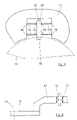
- FIG. 1 shows a schematic view of a projection exposure machine
- FIG. 2 shows a perspective view of a retaining structure
- FIG. 3 shows a schematic top view of the retaining structure according to FIG. 2 ;
- FIG. 4 shows a side view of a retaining structure.
- FIG. 1 shows a schematic view of a projection exposure machine 1 having an immersion lithography objective 2 that has a housing 3 in which a number of optical elements 4 are arranged.
- the projection exposure machine 1 also has at its top side a light source or an illumination system 5 that transmits a beam path 6 through the immersion lithography objective 2 and with the aid of which a reticle 7 arranged directly downstream of the illumination system 5 is imaged in a way known per se onto a wafer 8 located below the immersion lithography objective 1 .
- Semiconductor components are produced in a way likewise known per se by the exposure of the wafer 8 via the projection exposure machine 1 .
- a second or last optical element 10 Arranged downstream in the direction of the beam path 6 of the optical elements 4 specified above, which are held via respective mounts 9 in the housing 3 , is a second or last optical element 10 , which is fitted on the housing 3 via a retaining structure 11 .
- the last optical element 10 which can also be denoted as terminal element given that it is the optical element situated closest to the wafer 8 can be connected to the retaining structure 11 both rigidly and also exchangeably.
- an immersion medium 12 Located between the last optical element 10 and the wafer 8 is an immersion medium 12 that adjoins the second optical element 10 and covers the wafer 8 . Any suitable fluid, for example water, can be used as immersion medium 12 .
- the retaining structure 11 has a greater stiffness in the direction of the optical axis 13 than in a direction or plane perpendicular to the optical axis 13 .
- the stiffness of the retaining structure 11 in the direction of the optical axis 13 can be at least 10 7 N/m, while the stiffness of the retaining structure 11 in the direction perpendicular to the optical axis 13 , that is to say in the radial direction, can fall in the region of approximately 10 6 N/m or in a region stated below.
- the stiffness of the retaining structure 11 in the direction of the optical axis 13 can be at least four times the stiffness of the retaining structure 11 in the direction perpendicular to the optical axis 13 .
- the stiffness of the retaining structure 11 in the direction perpendicular to the optical axis 13 would be 2.5 ⁇ 10 6 N/m.
- the stiffness of the retaining structure 11 in the direction of the optical axis 13 can be at least forty times the stiffness in the direction perpendicular to the optical axis 13 , which would hence be 2.5 ⁇ 10 5 N/m.
- the relationship between the stiffness of the retaining structure 11 in the direction of the optical axis 13 can be as much as at least four hundred times the stiffness in the direction perpendicular to the optical axis 13 , which would then be 2.5 ⁇ 10 4 N/m.
- the stiffness of the retaining structure 11 in the direction of the optical axis 13 can differ from the above mentioned at least 10 7 N/m with the given relationships remaining and the stiffness of the retaining structure 11 in the direction perpendicular to the optical axis 13 changing.
- FIGS. 2 and 3 An embodiment of the retaining structure 11 that is to be regarded merely as exemplary is illustrated in FIGS. 2 and 3 and is capable of achieving the stiffnesses for the purpose of fitting the last optical element 10 .
- the last optical element 10 has on its outer edge a stiffening ring 14 that bears against a connecting element 15 . It suffices when a total of three connecting elements 15 are provided in the plane perpendicular to the optical axis 13 , but it is also possible to provide a larger number of connecting elements 15 .
- the connecting elements 15 are generally parallel to the stiffening ring 14 .
- the connecting element 15 which is of relatively large overall height and therefore extremely stiff in the direction of the optical axis 13 , is provided, for its part, with radially yielding or elastic decoupling elements 16 that ensure the lesser stiffness of the retaining structure 11 in the radial direction, that is to say in the direction or plane perpendicular to the optical axis 13 .
- the decoupling elements 16 can be regarded as joints or as relatively thin parts of the connecting elements 15 that assure the thermal expansion of the last optical element 10 .
- the retaining structure 11 also has an outer ring 17 , which has a coefficient of thermal expansion differing from the last optical element 10 , and which can consist, for example, of ceramic or titanium, but also of aluminum, steel or brass.
- the elastic decoupling elements 16 are arranged in the transitional region between the materials having the different coefficients of thermal expansion, that is to say between the last optical element 10 and the outer ring 17 .
- the connecting element 15 is an integral part with the outer ring 17 or, with other words, the stiffening ring 14 and the outer ring 17 are monolithic. Furthermore, the last optical element 10 rests on respective noses 18 of the connecting elements 15 .
- each connecting element 15 consists of two pairs of parallel bars 19 , which are connected to a central element 20 that comprises the nose 18 on which the last optical element 10 rests.
- Each of the bars 19 is coupled on one end to the outer ring 17 and on the other end to the central element 20 via a respective decoupling element 16 .
- This means that each connecting element 15 comprises eight joints or decoupling elements 16 .
- the retaining structure 11 also comprises the outer ring 17 , which can be joined to the last optical element 10 by soldering or wringing.
- the outer ring 17 comprises on each circumference three holes 21 , in which respective connecting elements 15 to connect the outer ring 17 with the housing 3 are contained. While these connecting elements are extremely stiff in the direction of the optical axis 13 , they comprise a rather weak portion forming the elastic decoupling element, which ensures the lesser stiffness of the retaining structure 11 in the radial direction to provide the possibility of a thermal extension of the last optical element 10 and the retaining structure 11 .
- the latter can also have, for example, a number of hexapods that are relatively stiff in the direction of the optical axis 13 and relatively elastic in the plane perpendicular to the optical axis 13 .
Landscapes
- Physics & Mathematics (AREA)
- General Physics & Mathematics (AREA)
- Health & Medical Sciences (AREA)
- Engineering & Computer Science (AREA)
- Environmental & Geological Engineering (AREA)
- Epidemiology (AREA)
- Public Health (AREA)
- Exposure And Positioning Against Photoresist Photosensitive Materials (AREA)
- Lens Barrels (AREA)
- Exposure Of Semiconductors, Excluding Electron Or Ion Beam Exposure (AREA)
Abstract
Description
Claims (10)
Priority Applications (1)
| Application Number | Priority Date | Filing Date | Title |
|---|---|---|---|
| US12/019,830 US7649702B2 (en) | 2005-08-16 | 2008-01-25 | Immersion lithography objective |
Applications Claiming Priority (3)
| Application Number | Priority Date | Filing Date | Title |
|---|---|---|---|
| US70881005P | 2005-08-16 | 2005-08-16 | |
| PCT/EP2006/008073 WO2007020067A1 (en) | 2005-08-16 | 2006-08-16 | Immersion lithography objective |
| US12/019,830 US7649702B2 (en) | 2005-08-16 | 2008-01-25 | Immersion lithography objective |
Related Parent Applications (1)
| Application Number | Title | Priority Date | Filing Date |
|---|---|---|---|
| PCT/EP2006/008073 Continuation WO2007020067A1 (en) | 2005-08-16 | 2006-08-16 | Immersion lithography objective |
Publications (2)
| Publication Number | Publication Date |
|---|---|
| US20080212211A1 US20080212211A1 (en) | 2008-09-04 |
| US7649702B2 true US7649702B2 (en) | 2010-01-19 |
Family
ID=37503663
Family Applications (1)
| Application Number | Title | Priority Date | Filing Date |
|---|---|---|---|
| US12/019,830 Expired - Fee Related US7649702B2 (en) | 2005-08-16 | 2008-01-25 | Immersion lithography objective |
Country Status (3)
| Country | Link |
|---|---|
| US (1) | US7649702B2 (en) |
| JP (1) | JP5243957B2 (en) |
| WO (1) | WO2007020067A1 (en) |
Families Citing this family (6)
| Publication number | Priority date | Publication date | Assignee | Title |
|---|---|---|---|---|
| DE102008026979B3 (en) * | 2008-05-29 | 2009-12-24 | Carl Zeiss Ag | Device for correcting image defect in optical system, has multiple optical components, which are arranged along common axis, where unit is provided for adjusting position of optical element |
| JP5455516B2 (en) * | 2009-09-11 | 2014-03-26 | キヤノン株式会社 | Support apparatus, optical apparatus, transfer apparatus, and device manufacturing method |
| DE102009045163B4 (en) * | 2009-09-30 | 2017-04-06 | Carl Zeiss Smt Gmbh | Optical arrangement in a microlithographic projection exposure apparatus |
| DE102010008756A1 (en) * | 2010-02-17 | 2011-06-30 | Carl Zeiss Laser Optics GmbH, 73447 | Optical arrangement for use in optical systems for correction of aberrations, has optical element and holder at which optical element is fixed, where optical element is fixed at holder by flexible bearing |
| CN102981234A (en) * | 2012-12-12 | 2013-03-20 | 中国科学院长春光学精密机械与物理研究所 | Axial adjustment device for optical element |
| DE102013201264A1 (en) * | 2013-01-28 | 2014-02-27 | Carl Zeiss Smt Gmbh | Connection assembly for connecting e.g. lens with temperature sensor of optical imaging device in microlithography applications, has connector comprising contact elements, where connector and optic element are connected by bonded connection |
Citations (14)
| Publication number | Priority date | Publication date | Assignee | Title |
|---|---|---|---|---|
| EP0023243A1 (en) | 1979-07-27 | 1981-02-04 | Combustion Engineering, Inc. | Apparatus and method for the disposal of rejects from a pulverizer of a coal-fired steamgenerator |
| US4733945A (en) | 1986-01-15 | 1988-03-29 | The Perkin-Elmer Corporation | Precision lens mounting |
| US6191898B1 (en) | 1999-01-15 | 2001-02-20 | Carl-Zeiss-Stiftung | Optical imaging device, particularly an objective, with at least one optical element |
| US6198576B1 (en) * | 1998-07-16 | 2001-03-06 | Nikon Corporation | Projection optical system and exposure apparatus |
| EP1081521A2 (en) | 1999-08-31 | 2001-03-07 | Nikon Corporation | Kinematic lens mounting |
| US20010039126A1 (en) | 2000-03-30 | 2001-11-08 | Ryuichi Ebinuma | Supporting structure of optical element, exposure apparatus having the same, and manufacturing method of semiconductor device |
| US20020021503A1 (en) | 2000-06-17 | 2002-02-21 | Karlfrid Osterried | Device for mounting an optical element, for example a lens element in a lens |
| US20020167740A1 (en) | 2001-05-02 | 2002-11-14 | Karlfrid Osterried | Lens system, in particular a projection lens system for semiconductor lithography |
| EP1279984A1 (en) | 2000-03-31 | 2003-01-29 | Nikon Corporation | Method and device for holding optical member, optical device, exposure apparatus, and device manufacturing method |
| US20030234918A1 (en) | 2002-06-20 | 2003-12-25 | Nikon Corporation | Adjustable soft mounts in kinematic lens mounting system |
| WO2004086148A1 (en) | 2003-03-26 | 2004-10-07 | Carl Zeiss Smt Ag | Device for the low-deformation replaceable mounting of an optical element |
| EP1503244A1 (en) | 2003-07-28 | 2005-02-02 | ASML Netherlands B.V. | Lithographic projection apparatus and device manufacturing method |
| US20050068499A1 (en) * | 2003-05-30 | 2005-03-31 | Carl Zeiss Smt Ag | Microlithographic projection exposure apparatus |
| US20050286146A1 (en) | 2004-04-13 | 2005-12-29 | Carl Zeiss Smt Gmbh | Closing module for an optical arrangement |
Family Cites Families (6)
| Publication number | Priority date | Publication date | Assignee | Title |
|---|---|---|---|---|
| JPH11337795A (en) * | 1998-05-22 | 1999-12-10 | Canon Inc | Lens barrel |
| JP2003029116A (en) * | 2001-07-13 | 2003-01-29 | Canon Inc | Lens holding device and projection exposure apparatus incorporating the lens holding device |
| JP4565261B2 (en) * | 2002-06-24 | 2010-10-20 | 株式会社ニコン | Optical element holding mechanism, optical system barrel, and exposure apparatus |
| EP2950148B1 (en) * | 2003-04-10 | 2016-09-21 | Nikon Corporation | Environmental system including vaccum scavenge for an immersion lithography apparatus |
| JP3805323B2 (en) * | 2003-05-21 | 2006-08-02 | キヤノン株式会社 | Exposure apparatus, aberration reduction method, and optical member adjustment mechanism |
| EP1695148B1 (en) * | 2003-11-24 | 2015-10-28 | Carl Zeiss SMT GmbH | Immersion objective |
-
2006
- 2006-08-16 WO PCT/EP2006/008073 patent/WO2007020067A1/en not_active Ceased
- 2006-08-16 JP JP2008526437A patent/JP5243957B2/en active Active
-
2008
- 2008-01-25 US US12/019,830 patent/US7649702B2/en not_active Expired - Fee Related
Patent Citations (14)
| Publication number | Priority date | Publication date | Assignee | Title |
|---|---|---|---|---|
| EP0023243A1 (en) | 1979-07-27 | 1981-02-04 | Combustion Engineering, Inc. | Apparatus and method for the disposal of rejects from a pulverizer of a coal-fired steamgenerator |
| US4733945A (en) | 1986-01-15 | 1988-03-29 | The Perkin-Elmer Corporation | Precision lens mounting |
| US6198576B1 (en) * | 1998-07-16 | 2001-03-06 | Nikon Corporation | Projection optical system and exposure apparatus |
| US6191898B1 (en) | 1999-01-15 | 2001-02-20 | Carl-Zeiss-Stiftung | Optical imaging device, particularly an objective, with at least one optical element |
| EP1081521A2 (en) | 1999-08-31 | 2001-03-07 | Nikon Corporation | Kinematic lens mounting |
| US20010039126A1 (en) | 2000-03-30 | 2001-11-08 | Ryuichi Ebinuma | Supporting structure of optical element, exposure apparatus having the same, and manufacturing method of semiconductor device |
| EP1279984A1 (en) | 2000-03-31 | 2003-01-29 | Nikon Corporation | Method and device for holding optical member, optical device, exposure apparatus, and device manufacturing method |
| US20020021503A1 (en) | 2000-06-17 | 2002-02-21 | Karlfrid Osterried | Device for mounting an optical element, for example a lens element in a lens |
| US20020167740A1 (en) | 2001-05-02 | 2002-11-14 | Karlfrid Osterried | Lens system, in particular a projection lens system for semiconductor lithography |
| US20030234918A1 (en) | 2002-06-20 | 2003-12-25 | Nikon Corporation | Adjustable soft mounts in kinematic lens mounting system |
| WO2004086148A1 (en) | 2003-03-26 | 2004-10-07 | Carl Zeiss Smt Ag | Device for the low-deformation replaceable mounting of an optical element |
| US20050068499A1 (en) * | 2003-05-30 | 2005-03-31 | Carl Zeiss Smt Ag | Microlithographic projection exposure apparatus |
| EP1503244A1 (en) | 2003-07-28 | 2005-02-02 | ASML Netherlands B.V. | Lithographic projection apparatus and device manufacturing method |
| US20050286146A1 (en) | 2004-04-13 | 2005-12-29 | Carl Zeiss Smt Gmbh | Closing module for an optical arrangement |
Also Published As
| Publication number | Publication date |
|---|---|
| JP5243957B2 (en) | 2013-07-24 |
| WO2007020067A1 (en) | 2007-02-22 |
| US20080212211A1 (en) | 2008-09-04 |
| JP2009505411A (en) | 2009-02-05 |
Similar Documents
| Publication | Publication Date | Title |
|---|---|---|
| EP1695148B1 (en) | Immersion objective | |
| TWI402551B (en) | Optical element holding apparatus | |
| US7649702B2 (en) | Immersion lithography objective | |
| US7154684B2 (en) | Optical element holding apparatus | |
| US8514371B2 (en) | Imaging device in a projection exposure facility | |
| JP5886952B2 (en) | Optical imaging device having individually actively supported components | |
| US9891535B2 (en) | Optical projection system | |
| US20090122288A1 (en) | Device for the low-deformation replaceable mounting of an optical element | |
| US10520838B2 (en) | Mounting arrangement for an optical imaging arrangement | |
| US9804500B2 (en) | Optical imaging arrangement with simplified manufacture | |
| KR20120073309A (en) | Optical arrangement in a microlithographic projection exposure apparatus | |
| US9250417B2 (en) | Optical arrangement in a microlithographic projection exposure apparatus | |
| CN105739248B (en) | Optical element support structure, unit microscope group, exposure optical system and litho machine | |
| WO2009124590A1 (en) | Optical aperture device | |
| CN113811820A (en) | Supporting optical elements | |
| CN120359471A (en) | Optical system and projection exposure apparatus | |
| JP7526192B2 (en) | Optical element support | |
| US20250138302A1 (en) | Optical assembly, projection exposure system for semiconductor lithography, and method |
Legal Events
| Date | Code | Title | Description |
|---|---|---|---|
| AS | Assignment |
Owner name: ASML NETHERLANDS B.V., NETHERLANDS Free format text: ASSIGNMENT OF ASSIGNORS INTEREST;ASSIGNORS:GELLRICH, BERNHARD;GRAEUPNER, PAUL;FISCHER, JUERGEN;AND OTHERS;REEL/FRAME:020714/0556;SIGNING DATES FROM 20080227 TO 20080317 Owner name: CARL ZEISS SMT AG, GERMANY Free format text: ASSIGNMENT OF ASSIGNORS INTEREST;ASSIGNORS:GELLRICH, BERNHARD;GRAEUPNER, PAUL;FISCHER, JUERGEN;AND OTHERS;REEL/FRAME:020714/0556;SIGNING DATES FROM 20080227 TO 20080317 Owner name: ASML NETHERLANDS B.V., NETHERLANDS Free format text: ASSIGNMENT OF ASSIGNORS INTEREST;ASSIGNORS:GELLRICH, BERNHARD;GRAEUPNER, PAUL;FISCHER, JUERGEN;AND OTHERS;SIGNING DATES FROM 20080227 TO 20080317;REEL/FRAME:020714/0556 Owner name: CARL ZEISS SMT AG, GERMANY Free format text: ASSIGNMENT OF ASSIGNORS INTEREST;ASSIGNORS:GELLRICH, BERNHARD;GRAEUPNER, PAUL;FISCHER, JUERGEN;AND OTHERS;SIGNING DATES FROM 20080227 TO 20080317;REEL/FRAME:020714/0556 |
|
| FEPP | Fee payment procedure |
Free format text: PAYOR NUMBER ASSIGNED (ORIGINAL EVENT CODE: ASPN); ENTITY STATUS OF PATENT OWNER: LARGE ENTITY |
|
| STCF | Information on status: patent grant |
Free format text: PATENTED CASE |
|
| AS | Assignment |
Owner name: CARL ZEISS SMT GMBH, GERMANY Free format text: A MODIFYING CONVERSION;ASSIGNOR:CARL ZEISS SMT AG;REEL/FRAME:025763/0367 Effective date: 20101014 |
|
| FPAY | Fee payment |
Year of fee payment: 4 |
|
| FPAY | Fee payment |
Year of fee payment: 8 |
|
| FEPP | Fee payment procedure |
Free format text: MAINTENANCE FEE REMINDER MAILED (ORIGINAL EVENT CODE: REM.); ENTITY STATUS OF PATENT OWNER: LARGE ENTITY |
|
| LAPS | Lapse for failure to pay maintenance fees |
Free format text: PATENT EXPIRED FOR FAILURE TO PAY MAINTENANCE FEES (ORIGINAL EVENT CODE: EXP.); ENTITY STATUS OF PATENT OWNER: LARGE ENTITY |
|
| STCH | Information on status: patent discontinuation |
Free format text: PATENT EXPIRED DUE TO NONPAYMENT OF MAINTENANCE FEES UNDER 37 CFR 1.362 |
|
| FP | Lapsed due to failure to pay maintenance fee |
Effective date: 20220119 |