US6201266B1 - Semiconductor device and method for manufacturing the same - Google Patents
Semiconductor device and method for manufacturing the same Download PDFInfo
- Publication number
- US6201266B1 US6201266B1 US09/460,984 US46098499A US6201266B1 US 6201266 B1 US6201266 B1 US 6201266B1 US 46098499 A US46098499 A US 46098499A US 6201266 B1 US6201266 B1 US 6201266B1
- Authority
- US
- United States
- Prior art keywords
- semiconductor device
- semiconductor
- bumps
- backside surface
- terminals
- Prior art date
- Legal status (The legal status is an assumption and is not a legal conclusion. Google has not performed a legal analysis and makes no representation as to the accuracy of the status listed.)
- Expired - Fee Related
Links
Images


Classifications
-
- H10W70/68—
-
- H10W74/117—
-
- H10W90/00—
-
- H10P72/7422—
-
- H10W70/60—
-
- H10W70/682—
-
- H10W70/685—
-
- H10W72/01331—
-
- H10W72/07236—
-
- H10W72/073—
-
- H10W72/075—
-
- H10W72/536—
-
- H10W72/5363—
-
- H10W72/552—
-
- H10W72/5522—
-
- H10W72/877—
-
- H10W72/884—
-
- H10W72/922—
-
- H10W72/923—
-
- H10W72/9415—
-
- H10W72/942—
-
- H10W74/00—
-
- H10W74/15—
-
- H10W90/288—
-
- H10W90/291—
-
- H10W90/722—
-
- H10W90/724—
-
- H10W90/734—
-
- H10W90/754—
Definitions
- the present invention relates to a semiconductor device and a method for manufacturing the same.
- the semiconductor device of the resin sealed type to be fitted to the portable electronic apparatus has been required to have a configuration which is thinner in thickness, smaller in size and lighter in weight.
- a chip size packaged (CSP) semiconductor device as a high-densely fabricated semiconductor device.
- An advanced semiconductor device generally includes several different semiconductor elements or devices respectively playing different roles, for instance a role of executing the memory processing, a role of performing the logic processing and so forth. Accordingly, the condition for manufacturing these different semiconductor elements or devices has to be naturally changed based on their different roles and functions. However, it would be difficult in general to provide a single semiconductor element or device with such different roles and functions. In order to obviate this difficulty, the following way has been taken so far, that is, separately manufacturing semiconductor elements or devices with respect to every necessary function, and then organizing semiconductor elements or devices having different functions by packaging them on a single printed board.
- the present invention has been made in view of the above problems that the prior art semiconductor devices are still encountering, and the object thereof is to provide a novel and improved semiconductor device and a method for manufacturing the same, according to which it is made possible to provide high-densely packaged semiconductor devices without lowering the final manufacturing yield thereof.
- a semiconductor device which includes the first semiconductor device having a plurality of bumps formed on the backside surface thereof; the second semiconductor device having a plurality of terminals formed on the front surface thereof so as to be electrically connected with the bumps, the second semiconductor device being mounted on an area which is located on the backside surface of the first semiconductor device and has no bump therein; wherein the height of the second semiconductor device measured from the backside surface of the first semiconductor device is made lower than the height of the bump.
- the second semiconductor device may be mounted on the first semiconductor device such that the surface provided with no terminal of the second semiconductor device is joined to the backside surface of the first semiconductor device with the help of an adhesive.
- a recess which is formed in a predetermined area provided with no bump of the first semiconductor device and the second semiconductor may be mounted on the recess.
- the recess is formed as a shallow spot facing portion which is flatly shaved so as to fit the size of the second semiconductor device.
- This predetermined temperature is a temperature which is employed in the heat treatment for packaging the second semiconductor device on the first semiconductor device, for instance a temperature of 200° C. or more.
- the second semiconductor device may be mounted on the first semiconductor device such that terminals of the second semiconductor device are joined to the backside surface of the first semiconductor device by means of soldered joints.
- a high heat-conductive adhesive member may be stuck on the surface provided with no terminal of the second semiconductor device.
- This adhesive member may be a sheet-like member having a predetermined thickness.
- the melting point of the soldered joint is preferably selected to be higher than a temperature employed in the heat treatment for packaging the second semiconductor device on the first semiconductor device, for instance 200° C. or more.
- the second semiconductor device may be mounted on the first semiconductor device such that the backside surface of the second semiconductor device is joined to the backside surface of the first semiconductor device with the help of a sealing resin.
- a method for manufacturing a semiconductor device including the first semiconductor device having a plurality of bumps which are formed on the backside surface thereof, and the second semiconductor device having a plurality of terminals which are formed on the front surface thereof and are to be electrically connected with the bumps, the second semiconductor device being mounted on an area which is located on the backside surface of the first semiconductor device without having any bump formed thereon, the method including the steps of: forming a plurality of bumps on the backside surface of the base plate for the first semiconductor device; placing a plurality of the second semiconductor devices on a mounting tape; mounting a plurality of the second semiconductor devices which are placed on the mounting tape, on the base plate; and dividing the base plate thereby obtaining a plurality of finished semiconductor devices including the first and second semiconductor devices.
- the step of placing a plurality of second semiconductor devices on the mounting tape further includes the steps of: forming a plurality of terminals on a semiconductor substrate; applying a sealing resin to the semiconductor substrate to cover the entire surface thereof on which terminals are exposed and polishing the sealing resin surface after the sealing resin has been completely cured until all the surfaces of terminals are exposed; forming a plurality of slits by cutting in the sealing resin until the cutting goes into the semiconductor substrate by a predetermined depth; applying an adhesive retaining tape to the surface of the polished sealing resin; polishing the backside surface of the semiconductor substrate until reaching all the bottoms of slots; sticking a mounting tape on the polished surface of the semiconductor substrate; and removing the adhesive retaining tape.
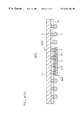
- FIGS. 1A and 1B are cross-sectional views for explaining the structure of an entire semiconductor device according to the first embodiment of the invention, including the first and second semiconductor devices.
- FIG. 2 is an enlarged cross-sectional view for explaining the structure of the second semiconductor device to be mounted on the first semiconductor device as shown in FIG. 1 .
- FIGS. 3A through 3C show diagrams for explaining the steps of manufacturing the first semiconductor device.
- FIGS. 4A through 4G show diagrams for explaining the steps of manufacturing the second semiconductor device.
- FIGS. 5A and 5B shows diagrams for explaining an application example of the first embodiment according to the invention.
- FIGS. 6A and 6B are cross-sectional views for explaining the structure of an entire semiconductor device according to the second embodiment of the invention.
- FIGS. 7A and 7B are cross-sectional views for explaining the structure of an entire semiconductor device according to the third embodiment of the invention.
- FIGS. 8A and 8B are cross-sectional views for explaining the structure of an entire semiconductor device according to the fourth embodiment of the invention.
- FIGS. 9A and 9B show diagrams for explaining an application example of the fourth embodiment according to the invention.
- FIGS. 10A and 10B are cross-sectional views for explaining the structure of an entire semiconductor device according to the fifth embodiment of the invention.
- FIGS. 11A and 11B are cross-sectional views for explaining the structure of an entire semiconductor device according to the sixth embodiment of the invention.
- FIG. 12 is a cross-sectional view for explaining the structure of an entire semiconductor device according to the seventh embodiment of the invention.
- a semiconductor device 100 according to this embodiment will now be described with reference to FIGS. 1A and 1B.
- the semiconductor device 100 includes the first ball grid array (BGA) semiconductor devices (simply referred to as the first semiconductor device hereinafter, unless needed to specially identify BGA) 110 and the second chip size package (CSP) semiconductor device (simply referred to as the second semiconductor device hereinafter, unless needed to specially identify CSP) 120 .
- the first semiconductor device 110 includes a base plate 16 made of a epoxy resin, a semiconductor element 1 a and thin metal wires 15 a , both being mounted on one surface of the base plate 16 , and a sealing resin 5 a applied to the one surface of the base plate 16 so as to entirely cover it along with the semiconductor element 1 a and thin metal wires 15 a .
- the second semiconductor device 120 includes a plurality of terminals 2 and is mounted in an area located on the backside surface of the base plate 16 , the area having no bump 3 formed therein. These bumps 3 of the first semiconductor device 110 and the terminals 2 of the second semiconductor device 120 are electrically connected with each other by means of printed wiring formed on another printed board 13 when the semiconductor device 100 is mounted on the printed board 13 in the later manufacturing step.
- the second semiconductor device 120 includes a semiconductor element 1 b having a thickness of about 400 ⁇ m, a plurality of electrode pads 6 formed on the semiconductor element 1 b , and a plurality of wiring 2 which are made of copper or the like to be electrically connected with electrode pads.
- the surface of the semiconductor element 1 b and the wiring 2 are sealed with the help of the sealing resin 5 b having a thickness of about 100 ⁇ m.
- the upper surface of the wiring 2 exposing from the surface of the sealing resin 5 b is treated with solder, thereby forming the bump 3 .
- a reference numeral 4 represents an additional wiring made of copper or the like for connecting the electrode pad 6 with the wiring 2 .
- the semiconductor element 1 a and wiring 14 are provided on the surface of the epoxy base plate 16 .
- the electrode formed on the semiconductor element 1 a is connected with the wiring 14 by means of the thin metal wires 15 a .
- the sealing resin 5 b is applied to one side of the epoxy base plate 16 so as to cover all the structural elements mounted on the epoxy base plate 16 .
- the bumps 3 are formed on the backside of the epoxy base plate 16 as shown in FIG. 1 . Since the epoxy base plate 16 includes a plurality of through holes 17 , the wiring 14 is electrically connected with the corresponding bumps 3 , respectively.
- the height of the bump 3 is preferably made to be a height substantially equal to or a little higher than the height of the second semiconductor device 120 to be mounted on the first semiconductor device 110 later. Bumps 3 will be melted in the course of the heat treatment that will be executed later for mounting the semiconductor device 100 on the printed board 13 .
- FIG. 4A a plurality of wiring 2 made of copper are formed on the surface of the semiconductor element 1 b by means of electroplating or the like such that the wiring has a height of about 50 ⁇ m.
- the sealing resin 5 b is applied to the entire surface of the semiconductor element 1 b so as to completely cover all the wiring 2 .
- This step of sealing with the resin may be carried out by employing a pertinent method, for instance the transfer mold method, the potting method, the printing method and so forth. After completely curing the applied sealing resin, the entire surface of the sealing resin is polished until the surface of each wiring 2 is exposed as shown in FIG. 4 C.
- FIG. 4D there are formed a plurality of slits 9 which extend from the sealing resin surface to the inside of the semiconductor element 1 b by a predetermined depth.
- These slits 9 are used for dividing the semiconductor element 1 b into a predetermined number of individual semiconductor element parts with wiring 2 (referred to as “semiconductor element 1 b ”′ hereinafter) in the later manufacturing step.
- the depth of the slit 9 can be determined by taking account of the thickness of the semiconductor element 1 b ′.
- the cutting of the slit is carried out such that the slit cutting distance or the slit depth exceeds the above designed thickness, for instance, by 20 ⁇ m or so. Consequently, it is determined that the actual slit depth to be cut is to be 170 ⁇ m by taking account of the sealing resin thickness of 50 ⁇ m.
- the next step is to polish the backside surface of the semiconductor element 1 b .
- an adhesive retaining tape 20 is applied to the resin surface side of the semiconductor element 1 b including slits 9 cut therein to.
- the adhesive retaining tape 20 is used for the purpose of holding each of semiconductor elements 1 b ′ to remain on the tape even after the semiconductor element 1 b is divided. Also, this tape 20 loses its adhesive strength when it is irradiated by ultra-violet light rays, so that it can be removed relatively with ease from the tape applied surface.
- the semiconductor element 1 b is mounted and fixed on a polishing means (not shown) by sucking the retaining tape side of the semiconductor element 1 b .
- the polishing step is continued, as shown in FIG. 4F, until it reaches the bottom of each of slits 9 , thereby individually divided semiconductor elements 1 b ′ (i.e. the second semiconductor devices 120 ) coming to align on the adhesive retaining tape 20 , eventually.
- a mounting tape 21 is applied to the polished surface while the retaining tape 20 is removed by irradiating it with ultra-violet light rays.
- the second semiconductor devices 120 aligned on the mounting tape 21 are mounted on the first semiconductor device 110 as they are.
- the second semiconductor device 120 is mounted on the area of the first semiconductor device 110 in which no bump 3 is formed, with the help of an adhesive 115 .
- the adhesive may be applied to either the area of the first semiconductor device 110 or the mounting tape 21 .
- the semiconductor device 100 is further packaged on the printed board 13 as shown in FIG. 1 B.
- the terminals 2 of the second semiconductor device 120 are electrically connected with printed board 13 through corresponding soldered joints 18 , respectively.
- These soldered joints 18 are made of solder paste, which are painted on the printed board 13 in advance such that they are arranged so as to correspond to bumps 3 and terminals 2 .
- the second semiconductor device 120 is mounted on the area which is located on the backside surface of the first semiconductor device 110 that includes no bump 3 . Moreover, both of the first and second semiconductors devices 110 and 120 are packaged into the first semiconductor device 100 in the state that they have already passed their final functional tests. Therefore, the high density package can be obtained without lowering the production yield.
- the first BGA semiconductor device may be constructed as the first CSP semiconductor device 110 ′ similar to the second CSP semiconductor device 120 .
- the first CSP semiconductor device 110 ′ includes an area similar to that of the first BGA semiconductor 110 , for mounting the second CSP semiconductor device 120 thereon. In this case, the area is provided with neither electrode 2 nor bump 3 .
- the structure similar to this is applicable to the embodiments described in the following.
- a semiconductor device 200 according to the second embodiment results from improvement of the semiconductor device 100 according to the first embodiment of the invention.
- a common point between semiconductor devices 200 and 100 exists in that the surface having no terminal of the second semiconductor device 220 is joined to the backside surface of the first semiconductor device 210 with the help of an adhesive 115 , thereby mounting the second semiconductor device 220 on the first semiconductor device 210 .
- the improved point of the semiconductor 200 will be described with reference to FIGS. 6A and 6B.
- the structural elements almost identical to those described in the previous embodiment are designated by like reference numerals or marks.
- the first semiconductor device 210 of the semiconductor device 200 includes an area on which the second semiconductor device 220 is mounted. This area is defined at a predetermined portion and is formed as a shallow flat recess (spot facing portion) 215 having a size corresponding to the size of the second semiconductor device 220 .
- the semiconductor device 200 is mounted on the printed board 13 in the later manufacturing step.
- the spot facing portion 215 can accommodate the second semiconductor device 220 at least in part, so that there may be widened a space between the second semiconductor device 220 and the printed board 13 .
- a plurality of bumps 3 b made of solder or the like can be formed in this space, thereby being able to enhance reliability with regard to the electrical connection between electrical elements.
- the area for mounting the second semiconductor device 220 thereon can have a wide space extended in its thickness direction. Consequently, even if the second semiconductor device 220 is a little thicker, the widened space can absorb that thickness at least in part, thus the spot facing portion 215 allowing the thicker second semiconductor device 220 to be accommodated therein. Also, with the formation of solder made bumps 3 b in the widened space, it is made possible to enhance reliability with regard to the electrical connection between electrical elements.
- a semiconductor device 300 according to this embodiment results from improvement of the semiconductor device 100 according to the first embodiment.
- a common point between the semiconductor devices 300 and 100 exists in that the surface having no terminal of the second semiconductor device 320 is joined to the backside surface of the first semiconductor device 310 with the help of an adhesive, thereby mounting the second semiconductor device 320 on the first semiconductor device 310 .
- the improved point of the semiconductor 300 will be described with reference to FIG. 7 . Again, in order to avoid redundant repetition of detailed descriptions, the structural elements almost identical to those described in previous embodiments are designated by like reference numerals or marks.
- the semiconductor device 300 shown in FIG. 7A is characterized by an adhesive 315 made of a low molecular material which is used for joining the backside surface of the second semiconductor device 320 to the first semiconductor device 310 .
- This adhesive loses its adhesive strength when it is heated exceeding a predetermined temperature such as 200° C. or more used in the heat treatment for the reflowing step in the process of mounting the semiconductor device 300 on the printed board 13 .
- the semiconductor 300 is mounted on the printed board 13 as shown in FIG. 7 B.
- the low molecular adhesive 315 loses its adhesive strength as mentioned above, and the first and second semiconductor devices 310 and 320 are separated from each other.
- the first and second semiconductor devices 310 and 320 are separated from each other, thus each positioning of them being carried out independently. With the effect of such self-alignment, both of the first and second semiconductor devices can be mounted on the printed board with the precise positioning, respectively.
- a semiconductor device 400 according to this embodiment will be described with reference to FIG. 8 . Again, in order to avoid repetitive redundant descriptions, the structural elements almost identical to those of the semiconductor device 100 are denoted with like numbers or marks.
- the surface having no terminal of the second semiconductor device 120 is joined to the backside surface of the first semiconductor device 110 with the help of the adhesive 115 , thereby mounting the second semiconductor 120 on the first semiconductor device 110 .
- the semiconductor device 400 is characterized in that the terminals 2 of the second semiconductor device 420 are joined to the backside surface of the first semiconductor device 410 through soldered joints 415 , thereby mounting the second semiconductor device 420 on the first semiconductor device 410 .
- an epoxy base plate 16 On the backside surface of an epoxy base plate 16 on which a plurality of bumps 3 are provided, there is formed a predetermined wiring pattern (not shown) which forms conductive paths between bumps 3 and corresponding terminals 2 of the second semiconductor device 420 . Therefor, according to this structure, the first and second semiconductor devices 410 and 420 are electrically connected with each other on the backside of the epoxy base plate 16 .
- the semiconductor device 400 As shown in FIG. 8B, at the stage of mounting it on the printed board 13 in the later manufacturing step, the number of terminals needed for the entire device is not increased, thus the step of mounting the semiconductor device 400 on the printing board 13 being carried out with ease.
- the fourth embodiment of the invention has been explained by way of the semiconductor device 400 which employs the first BGA semiconductor device 410 .
- the first BGA semiconductor device may be constructed as the first CSP semiconductor device 410 ′ similar to the second CSP semiconductor device 420 .
- the first CSP semiconductor device 410 ′ includes an area similar to that of the first BGA semiconductor 410 , for mounting the second CSP semiconductor device 420 thereon.
- the area includes no bumps 3 but electrodes 2 are exposed to the surface thereof, instead, and the terminals 2 of the first semiconductor device 410 ′ are electrically connected with the corresponding terminals 2 of the second semiconductor device 420 through soldered joints 415 .
- the structure similar to this is applicable to the embodiments described in the following.
- a semiconductor device 500 according to this embodiment results from improvement of the semiconductor device 400 according to the fourth embodiment.
- a common point between the semiconductor devices 500 and 400 exists in that the terminal of the second semiconductor device 520 is joined to the backside surface of the first semiconductor device 510 by means of soldered joints 415 , thereby mounting the second semiconductor device 520 on the first semiconductor device 510 .
- the improved point of the semiconductor 500 will be described with reference to FIG. 10 .
- the structural elements almost identical to those described in the previous embodiments are designated by like reference numerals or marks.
- the semiconductor device 500 is characterized by a high heat-conductive adhesive member 515 which is stuck on the backside surface of the second semiconductor device 520 .
- the adhesive member 515 is illustrated as a sheet-like member having a predetermined thickness.
- the semiconductor device 500 is mounted, as shown in FIG. 10B, on the printed board 13 in the later manufacturing step. At this time, the second semiconductor device 520 is fixed on the printed board 13 with the help of the adhesive strength of the adhesive member 515 .
- the second semiconductor device 520 is mounted on the printed board 13 with the help of the high heat-conductive adhesive member 515 , thus improving and facilitating the thermal radiation of the second semiconductor device 520 .
- a semiconductor device 600 according to this embodiment results from improvement of the semiconductor device 400 according to the fourth embodiment.
- a common point between the semiconductor devices 600 and 400 exists in that the terminal of the second semiconductor device 620 is joined to the backside surface of the first semiconductor device 610 by means of soldered joints, thereby mounting the second semiconductor device 620 on the first semiconductor device 610 .
- the improved point of the semiconductor 600 will be described with reference to FIG. 11 .
- the structural elements almost identical to those described in the previous embodiments are designated by like reference numerals or marks.
- the semiconductor device 600 is characterized by a high temperature solder 615 which is employed for joining the terminal of the second semiconductor device 620 with the first semiconductor device 610 .
- This high temperature solder 615 has a high melting point such as 200° C. or more, which is higher than the temperature employed in the course of the heat treatment executed in the later manufacturing step for mounting the semiconductor device 600 on the printed board 13 as shown in FIG. 11 B.
- the semiconductor device 600 if there is executed the heat treatment for the reflowing step in the process of mounting the semiconductor device 600 on the printed board 13 , the second semiconductor device 620 is still firmly joined to the first semiconductor 610 with the high temperature solder, thus enabling the semiconductor device 600 to be stably packaged on the printed board.
- a semiconductor device 700 according to this embodiment will now be described with reference to FIG. 12 .
- the structural elements almost identical to those of the semiconductor device 100 according to the first embodiment are designated by like reference numerals or marks.
- the second semiconductor device 120 is joined to the backside surface of the first semiconductor device 110 with the help of the adhesive 115 , thereby mounting the second semiconductor 120 on the first semiconductor device 110 .
- the semiconductor device 700 is characterized in that the second semiconductor device 720 is joined to the backside surface of the first semiconductor device 710 through a sealing resin 715 , thereby mounting the second semiconductor device 720 on the first semiconductor device 710 .
- the first semiconductor device 710 includes a semiconductor element la and an epoxy base plate 16 , on which there are provided a predetermined wiring pattern and, if needed, a heat radiation plate 702 .
- the semiconductor element la is fixed on the epoxy base plate 16 with the help of an adhesive while the electrodes on the semiconductor element la are connected with corresponding wiring pattern of the epoxy base plate 16 through thin metal wires 15 a , respectively.
- the surface of the epoxy base plate 16 is made conductive with the wiring patterns formed thereon, thus being electrically connected with corresponding bumps 3 which are arranged on the backside surface of the first semiconductor device 710 .
- the second semiconductor device 720 is mounted on the first semiconductor device 710 with the help of a sealing resin 715 .
- the sealing resin 715 is first applied to a predetermined portion (shown as a recess or spot facing portion in the figure) of the first semiconductor device 710 so as to seal the semiconductor element 1 a .
- the second semiconductor 720 is then put on the applied sealing resin before it is cured.
- the second semiconductor 720 is firmly joined together with the first semiconductor device 710 when the sealing resin 715 is completely cured.
- the second semiconductor device 720 is directly adhered to the sealing resin portion of the first semiconductor device 710 , so that there is no need for other fixing member such as an adhesive to be employed, thus the manufacturing steps being simplified and the manufacturing cost being reduced.
- the invention provides various advantages. That is, the invention makes it possible to execute the high-density packaging of semiconductor devices without lowering the final manufacturing yield thereof; to mount the semiconductor device on the printed board even if it has a little thicker dimension; to enhance reliability with regard to the connection between structural elements of the semiconductor device; to execute the precise positioning of semiconductor devices on the printed board; to facilitate the heat radiation of the semiconductor device; and to package the semiconductor devices on the printed board with high stability.
Landscapes
- Wire Bonding (AREA)
Abstract
Description
Claims (20)
Priority Applications (6)
| Application Number | Priority Date | Filing Date | Title |
|---|---|---|---|
| US09/757,663 US6673651B2 (en) | 1999-07-01 | 2001-01-11 | Method of manufacturing semiconductor device including semiconductor elements mounted on base plate |
| US10/657,139 US7723832B2 (en) | 1999-07-01 | 2003-09-09 | Semiconductor device including semiconductor elements mounted on base plate |
| US11/077,145 US7592690B2 (en) | 1999-07-01 | 2005-03-11 | Semiconductor device including semiconductor elements mounted on base plate |
| US11/077,152 US7427810B2 (en) | 1999-07-01 | 2005-03-11 | Semiconductor device including semiconductor element mounted on another semiconductor element |
| US12/759,919 US8008129B2 (en) | 1999-07-01 | 2010-04-14 | Method of making semiconductor device packaged by sealing resin member |
| US13/205,581 US8486728B2 (en) | 1999-07-01 | 2011-08-08 | Semiconductor device including semiconductor elements mounted on base plate |
Applications Claiming Priority (2)
| Application Number | Priority Date | Filing Date | Title |
|---|---|---|---|
| JP11-187658 | 1999-07-01 | ||
| JP18765899A JP3526788B2 (en) | 1999-07-01 | 1999-07-01 | Method for manufacturing semiconductor device |
Related Child Applications (1)
| Application Number | Title | Priority Date | Filing Date |
|---|---|---|---|
| US09/757,663 Division US6673651B2 (en) | 1999-07-01 | 2001-01-11 | Method of manufacturing semiconductor device including semiconductor elements mounted on base plate |
Publications (1)
| Publication Number | Publication Date |
|---|---|
| US6201266B1 true US6201266B1 (en) | 2001-03-13 |
Family
ID=16209936
Family Applications (7)
| Application Number | Title | Priority Date | Filing Date |
|---|---|---|---|
| US09/460,984 Expired - Fee Related US6201266B1 (en) | 1999-07-01 | 1999-12-15 | Semiconductor device and method for manufacturing the same |
| US09/757,663 Expired - Lifetime US6673651B2 (en) | 1999-07-01 | 2001-01-11 | Method of manufacturing semiconductor device including semiconductor elements mounted on base plate |
| US10/657,139 Expired - Fee Related US7723832B2 (en) | 1999-07-01 | 2003-09-09 | Semiconductor device including semiconductor elements mounted on base plate |
| US11/077,145 Expired - Fee Related US7592690B2 (en) | 1999-07-01 | 2005-03-11 | Semiconductor device including semiconductor elements mounted on base plate |
| US11/077,152 Expired - Fee Related US7427810B2 (en) | 1999-07-01 | 2005-03-11 | Semiconductor device including semiconductor element mounted on another semiconductor element |
| US12/759,919 Expired - Fee Related US8008129B2 (en) | 1999-07-01 | 2010-04-14 | Method of making semiconductor device packaged by sealing resin member |
| US13/205,581 Expired - Fee Related US8486728B2 (en) | 1999-07-01 | 2011-08-08 | Semiconductor device including semiconductor elements mounted on base plate |
Family Applications After (6)
| Application Number | Title | Priority Date | Filing Date |
|---|---|---|---|
| US09/757,663 Expired - Lifetime US6673651B2 (en) | 1999-07-01 | 2001-01-11 | Method of manufacturing semiconductor device including semiconductor elements mounted on base plate |
| US10/657,139 Expired - Fee Related US7723832B2 (en) | 1999-07-01 | 2003-09-09 | Semiconductor device including semiconductor elements mounted on base plate |
| US11/077,145 Expired - Fee Related US7592690B2 (en) | 1999-07-01 | 2005-03-11 | Semiconductor device including semiconductor elements mounted on base plate |
| US11/077,152 Expired - Fee Related US7427810B2 (en) | 1999-07-01 | 2005-03-11 | Semiconductor device including semiconductor element mounted on another semiconductor element |
| US12/759,919 Expired - Fee Related US8008129B2 (en) | 1999-07-01 | 2010-04-14 | Method of making semiconductor device packaged by sealing resin member |
| US13/205,581 Expired - Fee Related US8486728B2 (en) | 1999-07-01 | 2011-08-08 | Semiconductor device including semiconductor elements mounted on base plate |
Country Status (2)
| Country | Link |
|---|---|
| US (7) | US6201266B1 (en) |
| JP (1) | JP3526788B2 (en) |
Cited By (46)
| Publication number | Priority date | Publication date | Assignee | Title |
|---|---|---|---|---|
| US6437990B1 (en) * | 2000-03-20 | 2002-08-20 | Agere Systems Guardian Corp. | Multi-chip ball grid array IC packages |
| US6455786B1 (en) * | 1998-08-03 | 2002-09-24 | Shinko Electric Industries Co., Ltd. | Wiring board and manufacturing method thereof and semiconductor device |
| US6580169B2 (en) * | 1999-12-27 | 2003-06-17 | Fujitsu Limited | Method for forming bumps, semiconductor device, and solder paste |
| US20030178719A1 (en) * | 2002-03-22 | 2003-09-25 | Combs Edward G. | Enhanced thermal dissipation integrated circuit package and method of manufacturing enhanced thermal dissipation integrated circuit package |
| US20040056277A1 (en) * | 2002-09-17 | 2004-03-25 | Chippac, Inc. | Semiconductor multi-package module including stacked-die package and having wire bond interconnect between stacked packages |
| US20040063246A1 (en) * | 2002-09-17 | 2004-04-01 | Chippac, Inc. | Semiconductor multi-package module having package stacked over die-down flip chip ball grid array package and having wire bond interconnect between stacked packages |
| US20040061213A1 (en) * | 2002-09-17 | 2004-04-01 | Chippac, Inc. | Semiconductor multi-package module having package stacked over die-up flip chip ball grid array package and having wire bond interconnect between stacked packages |
| US20040061212A1 (en) * | 2002-09-17 | 2004-04-01 | Chippac, Inc. | Semiconductor multi-package module having wire bond interconnect between stacked packages |
| US20040063242A1 (en) * | 2002-09-17 | 2004-04-01 | Chippac, Inc. | Semiconductor multi-package module having package stacked over ball grid array package and having wire bond interconnect between stacked packages |
| US6737742B2 (en) | 2002-09-11 | 2004-05-18 | International Business Machines Corporation | Stacked package for integrated circuits |
| US20040145051A1 (en) * | 2003-01-27 | 2004-07-29 | Klein Dean A. | Semiconductor components having stacked dice and methods of fabrication |
| US6790710B2 (en) | 2002-01-31 | 2004-09-14 | Asat Limited | Method of manufacturing an integrated circuit package |
| US20050002167A1 (en) * | 2003-07-02 | 2005-01-06 | John Hsuan | Microelectronic package |
| US20050056944A1 (en) * | 2001-02-27 | 2005-03-17 | Chippac, Inc. | Super-thin high speed flip chip package |
| US20050110141A1 (en) * | 2003-10-27 | 2005-05-26 | Seiko Epson Corporation | Semiconductor device, its manufacturing method, circuit board, and electronic unit |
| US20050121773A1 (en) * | 2002-07-12 | 2005-06-09 | Oki Electric Industry Co. Ltd. | Method of manufacturing semiconductor device |
| US20050133916A1 (en) * | 2003-12-17 | 2005-06-23 | Stats Chippac, Inc | Multiple chip package module having inverted package stacked over die |
| US20050269676A1 (en) * | 2004-05-24 | 2005-12-08 | Chippac, Inc | Adhesive/spacer island structure for stacking over wire bonded die |
| US20060012018A1 (en) * | 2004-07-13 | 2006-01-19 | Chippac, Inc. | Semiconductor multipackage module including die and inverted land grid array package stacked over ball grid array package |
| US20060151206A1 (en) * | 2005-01-13 | 2006-07-13 | Sharp Kabushiki Kaisha | Semiconductor device and manufacturing method therefor |
| US20060220209A1 (en) * | 2005-03-31 | 2006-10-05 | Stats Chippac Ltd. | Semiconductor stacked package assembly having exposed substrate surfaces on upper and lower sides |
| US20060220210A1 (en) * | 2005-03-31 | 2006-10-05 | Stats Chippac Ltd. | Semiconductor assembly including chip scale package and second substrate and having exposed substrate surfaces on upper and lower sides |
| US20060244117A1 (en) * | 2005-04-29 | 2006-11-02 | Stats Chippac, Ltd. | Semiconductor package including second substrate and having exposed substrate surfaces on upper and lower sides |
| US20060249851A1 (en) * | 2005-05-05 | 2006-11-09 | Stats Chippac Ltd. | Multiple Chip Package Module Including Die Stacked Over Encapsulated Package |
| US20060284299A1 (en) * | 2005-06-20 | 2006-12-21 | Stats Chippac Ltd. | Module Having Stacked Chip Scale Semiconductor Packages |
| US20070015314A1 (en) * | 2004-05-24 | 2007-01-18 | Chippac, Inc | Adhesive/Spacer Island Structure for Multiple Die Package |
| US20070018296A1 (en) * | 2004-05-24 | 2007-01-25 | Chippac, Inc | Stacked Semiconductor Package having Adhesive/Spacer Structure and Insulation |
| US20070111388A1 (en) * | 2002-10-08 | 2007-05-17 | Chippac, Inc. | Semiconductor Multi-Package Module Having Inverted Second Package Stacked Over Die-Up Flip-Chip Ball Grid Array (BGA) Package |
| US20070158809A1 (en) * | 2006-01-04 | 2007-07-12 | Chow Seng G | Multi-chip package system |
| US20070158833A1 (en) * | 2006-01-04 | 2007-07-12 | Soo-San Park | Integrated circuit package system including stacked die |
| US20080023032A1 (en) * | 2006-07-25 | 2008-01-31 | The Acker-Cowan Group, L.L.C. | Acoustic ceiling removal |
| US20080124843A1 (en) * | 1999-12-27 | 2008-05-29 | Shinji Ohuchi | Resin for sealing semiconductor device, resin-sealed semiconductor device and the method of manufacturing the semiconductor device |
| US20080290496A1 (en) * | 2007-05-25 | 2008-11-27 | Nepes Corporation | Wafer level system in package and fabrication method thereof |
| US20090027863A1 (en) * | 2003-04-04 | 2009-01-29 | Marcos Karnezos | Method for making a semiconductor multipackage module including a processor and memory package assemblies |
| US20090057861A1 (en) * | 2007-08-31 | 2009-03-05 | Soo-San Park | Integrated circuit package-in-package system with side-by-side and offset stacking |
| US20090057864A1 (en) * | 2007-08-31 | 2009-03-05 | Daesik Choi | Integrated circuit package system employing an offset stacked configuration |
| US20090230532A1 (en) * | 2008-03-11 | 2009-09-17 | Stats Chippac Ltd | System for solder ball inner stacking module connection |
| US20100038771A1 (en) * | 2004-06-10 | 2010-02-18 | Il Kwon Shim | Integrated circuit package with open substrate |
| US7687315B2 (en) | 2005-04-29 | 2010-03-30 | Stats Chippac Ltd. | Stacked integrated circuit package system and method of manufacture therefor |
| US7750482B2 (en) | 2006-02-09 | 2010-07-06 | Stats Chippac Ltd. | Integrated circuit package system including zero fillet resin |
| US7855100B2 (en) | 2005-03-31 | 2010-12-21 | Stats Chippac Ltd. | Integrated circuit package system with an encapsulant cavity and method of fabrication thereof |
| US20110074028A1 (en) * | 2004-10-07 | 2011-03-31 | Stats Chippac, Ltd. | Semiconductor Device and Method of Dissipating Heat From Thin Package-on-Package Mounted to Substrate |
| US20120085575A1 (en) * | 2010-10-08 | 2012-04-12 | Nobuhiro Yamamoto | Electronic Apparatus Manufacturing Method, Electronic Component, and Electronic Apparatus |
| USRE44438E1 (en) | 2001-02-27 | 2013-08-13 | Stats Chippac, Ltd. | Semiconductor device and method of dissipating heat from thin package-on-package mounted to substrate |
| US8704349B2 (en) | 2006-02-14 | 2014-04-22 | Stats Chippac Ltd. | Integrated circuit package system with exposed interconnects |
| US20160064348A1 (en) * | 2014-08-27 | 2016-03-03 | Taiwan Semiconductor Manufacturing Company, Ltd. | Packaging Devices, Packaged Semiconductor Devices, and Packaging Methods |
Families Citing this family (43)
| Publication number | Priority date | Publication date | Assignee | Title |
|---|---|---|---|---|
| JP3526788B2 (en) * | 1999-07-01 | 2004-05-17 | 沖電気工業株式会社 | Method for manufacturing semiconductor device |
| JP3420748B2 (en) * | 2000-12-14 | 2003-06-30 | 松下電器産業株式会社 | Semiconductor device and manufacturing method thereof |
| JP4105409B2 (en) * | 2001-06-22 | 2008-06-25 | 株式会社ルネサステクノロジ | Multi-chip module manufacturing method |
| JP4649792B2 (en) * | 2001-07-19 | 2011-03-16 | 日本電気株式会社 | Semiconductor device |
| US7310458B2 (en) | 2001-10-26 | 2007-12-18 | Staktek Group L.P. | Stacked module systems and methods |
| US7656678B2 (en) * | 2001-10-26 | 2010-02-02 | Entorian Technologies, Lp | Stacked module systems |
| US6956284B2 (en) | 2001-10-26 | 2005-10-18 | Staktek Group L.P. | Integrated circuit stacking system and method |
| US7371609B2 (en) * | 2001-10-26 | 2008-05-13 | Staktek Group L.P. | Stacked module systems and methods |
| US6576992B1 (en) * | 2001-10-26 | 2003-06-10 | Staktek Group L.P. | Chip scale stacking system and method |
| US20030234443A1 (en) | 2001-10-26 | 2003-12-25 | Staktek Group, L.P. | Low profile stacking system and method |
| US6914324B2 (en) * | 2001-10-26 | 2005-07-05 | Staktek Group L.P. | Memory expansion and chip scale stacking system and method |
| US20040195666A1 (en) * | 2001-10-26 | 2004-10-07 | Julian Partridge | Stacked module systems and methods |
| US7485951B2 (en) * | 2001-10-26 | 2009-02-03 | Entorian Technologies, Lp | Modularized die stacking system and method |
| US20060255446A1 (en) * | 2001-10-26 | 2006-11-16 | Staktek Group, L.P. | Stacked modules and method |
| US6940729B2 (en) * | 2001-10-26 | 2005-09-06 | Staktek Group L.P. | Integrated circuit stacking system and method |
| US6952047B2 (en) * | 2002-07-01 | 2005-10-04 | Tessera, Inc. | Assemblies having stacked semiconductor chips and methods of making same |
| US20050161814A1 (en) * | 2002-12-27 | 2005-07-28 | Fujitsu Limited | Method for forming bumps, semiconductor device and method for manufacturing same, substrate processing apparatus, and semiconductor manufacturing apparatus |
| US7542304B2 (en) | 2003-09-15 | 2009-06-02 | Entorian Technologies, Lp | Memory expansion and integrated circuit stacking system and method |
| JP4353845B2 (en) * | 2004-03-31 | 2009-10-28 | 富士通株式会社 | Manufacturing method of semiconductor device |
| US20060043558A1 (en) * | 2004-09-01 | 2006-03-02 | Staktek Group L.P. | Stacked integrated circuit cascade signaling system and method |
| US7033861B1 (en) * | 2005-05-18 | 2006-04-25 | Staktek Group L.P. | Stacked module systems and method |
| US7576995B2 (en) * | 2005-11-04 | 2009-08-18 | Entorian Technologies, Lp | Flex circuit apparatus and method for adding capacitance while conserving circuit board surface area |
| US7508069B2 (en) | 2006-01-11 | 2009-03-24 | Entorian Technologies, Lp | Managed memory component |
| US7304382B2 (en) | 2006-01-11 | 2007-12-04 | Staktek Group L.P. | Managed memory component |
| US7605454B2 (en) | 2006-01-11 | 2009-10-20 | Entorian Technologies, Lp | Memory card and method for devising |
| US7508058B2 (en) * | 2006-01-11 | 2009-03-24 | Entorian Technologies, Lp | Stacked integrated circuit module |
| US20070158821A1 (en) * | 2006-01-11 | 2007-07-12 | Leland Szewerenko | Managed memory component |
| US7608920B2 (en) * | 2006-01-11 | 2009-10-27 | Entorian Technologies, Lp | Memory card and method for devising |
| US20070164416A1 (en) * | 2006-01-17 | 2007-07-19 | James Douglas Wehrly | Managed memory component |
| US20070262429A1 (en) * | 2006-05-15 | 2007-11-15 | Staktek Group, L.P. | Perimeter stacking system and method |
| US7468553B2 (en) * | 2006-10-20 | 2008-12-23 | Entorian Technologies, Lp | Stackable micropackages and stacked modules |
| US7417310B2 (en) | 2006-11-02 | 2008-08-26 | Entorian Technologies, Lp | Circuit module having force resistant construction |
| KR100817091B1 (en) * | 2007-03-02 | 2008-03-26 | 삼성전자주식회사 | Multilayer semiconductor package and manufacturing method thereof |
| GB0711676D0 (en) * | 2007-06-16 | 2007-07-25 | Rf Module And Optical Design L | Improvements relating to semiconductor packages |
| US9782660B2 (en) | 2007-11-30 | 2017-10-10 | Nike, Inc. | Athletic training system and method |
| DE102008009510B3 (en) * | 2008-02-15 | 2009-07-16 | Danfoss Silicon Power Gmbh | Method for low-temperature pressure sintering |
| JP2009302212A (en) | 2008-06-11 | 2009-12-24 | Fujitsu Microelectronics Ltd | Semiconductor device and method of manufacturing the same |
| US20110241125A1 (en) * | 2010-03-31 | 2011-10-06 | Semtech Corporation | Power Semiconductor Device with Low Parasitic Metal and Package Resistance |
| TWI553809B (en) * | 2014-06-24 | 2016-10-11 | 思鷺科技股份有限公司 | Package substrate structure |
| JP6865828B2 (en) * | 2017-07-12 | 2021-04-28 | 東京エレクトロン株式会社 | Transport equipment, substrate processing system, transport method, and substrate processing method |
| USD893441S1 (en) * | 2019-06-28 | 2020-08-18 | Applied Materials, Inc. | Base plate for a processing chamber substrate support |
| US11887878B2 (en) | 2019-06-28 | 2024-01-30 | Applied Materials, Inc. | Detachable biasable electrostatic chuck for high temperature applications |
| USD947914S1 (en) * | 2020-11-23 | 2022-04-05 | Applied Materials, Inc. | Base plate for a processing chamber substrate support |
Citations (2)
| Publication number | Priority date | Publication date | Assignee | Title |
|---|---|---|---|---|
| US5866949A (en) * | 1996-12-02 | 1999-02-02 | Minnesota Mining And Manufacturing Company | Chip scale ball grid array for integrated circuit packaging |
| US5925934A (en) * | 1995-10-28 | 1999-07-20 | Institute Of Microelectronics | Low cost and highly reliable chip-sized package |
Family Cites Families (43)
| Publication number | Priority date | Publication date | Assignee | Title |
|---|---|---|---|---|
| JPS5731166A (en) | 1980-07-31 | 1982-02-19 | Fujitsu Ltd | Semiconductor device |
| JPS59117146A (en) | 1982-12-24 | 1984-07-06 | Hitachi Ltd | Semiconductor integrated circuit |
| JP2734672B2 (en) | 1989-08-25 | 1998-04-02 | 旭硝子株式会社 | Method for producing 1,1-difluoroethane |
| US5200362A (en) | 1989-09-06 | 1993-04-06 | Motorola, Inc. | Method of attaching conductive traces to an encapsulated semiconductor die using a removable transfer film |
| JPH0438064A (en) | 1990-06-04 | 1992-02-07 | Nec Corp | Facsimile equipment |
| JPH05335411A (en) | 1992-06-02 | 1993-12-17 | Toshiba Corp | Pellet manufacturing method |
| US5467252A (en) * | 1993-10-18 | 1995-11-14 | Motorola, Inc. | Method for plating using nested plating buses and semiconductor device having the same |
| JPH07221262A (en) | 1994-02-07 | 1995-08-18 | Hitachi Ltd | Semiconductor module |
| JP3288840B2 (en) | 1994-02-28 | 2002-06-04 | 三菱電機株式会社 | Semiconductor device and manufacturing method thereof |
| JP2595909B2 (en) * | 1994-09-14 | 1997-04-02 | 日本電気株式会社 | Semiconductor device |
| TW318321B (en) | 1995-07-14 | 1997-10-21 | Matsushita Electric Industrial Co Ltd | |
| JP3264147B2 (en) * | 1995-07-18 | 2002-03-11 | 日立電線株式会社 | Semiconductor device, interposer for semiconductor device, and method of manufacturing the same |
| US5847455A (en) * | 1995-11-07 | 1998-12-08 | Vlsi Technology, Inc. | Molded leadframe ball grid array |
| US6404049B1 (en) * | 1995-11-28 | 2002-06-11 | Hitachi, Ltd. | Semiconductor device, manufacturing method thereof and mounting board |
| JP3466354B2 (en) | 1995-12-25 | 2003-11-10 | 新光電気工業株式会社 | Semiconductor device |
| US5668408A (en) * | 1996-04-12 | 1997-09-16 | Hewlett-Packard Company | Pin grid array solution for microwave multi-chip modules |
| JPH09321175A (en) * | 1996-05-30 | 1997-12-12 | Oki Electric Ind Co Ltd | Microwave circuits and chips |
| JPH1012810A (en) | 1996-06-26 | 1998-01-16 | Hitachi Ltd | Semiconductor device |
| JPH1093013A (en) | 1996-09-17 | 1998-04-10 | Seiko Epson Corp | Semiconductor device |
| JPH1098072A (en) * | 1996-09-20 | 1998-04-14 | Hitachi Ltd | Semiconductor device and manufacturing method thereof |
| US5867678A (en) * | 1996-12-16 | 1999-02-02 | International Business Machines Corporation | Method and system for searching and retrieving specific types of objects contained within a compound document |
| US6515370B2 (en) * | 1997-03-10 | 2003-02-04 | Seiko Epson Corporation | Electronic component and semiconductor device, method for manufacturing the same, circuit board have the same mounted thereon, and electronic equipment having the circuit board |
| JPH10270496A (en) * | 1997-03-27 | 1998-10-09 | Hitachi Ltd | Electronic device, information processing device, semiconductor device, and semiconductor chip mounting method |
| JPH10294423A (en) * | 1997-04-17 | 1998-11-04 | Nec Corp | Semiconductor device |
| US5880590A (en) * | 1997-05-07 | 1999-03-09 | International Business Machines Corporation | Apparatus and method for burn-in and testing of devices with solder bumps or preforms |
| JP3526731B2 (en) * | 1997-10-08 | 2004-05-17 | 沖電気工業株式会社 | Semiconductor device and manufacturing method thereof |
| US5861678A (en) * | 1997-12-23 | 1999-01-19 | Micron Technology, Inc. | Method and system for attaching semiconductor dice to substrates |
| JP3481444B2 (en) * | 1998-01-14 | 2003-12-22 | シャープ株式会社 | Semiconductor device and manufacturing method thereof |
| US6326696B1 (en) * | 1998-02-04 | 2001-12-04 | International Business Machines Corporation | Electronic package with interconnected chips |
| JP3173459B2 (en) * | 1998-04-21 | 2001-06-04 | 日本電気株式会社 | Method for manufacturing semiconductor device |
| JP3055619B2 (en) * | 1998-04-30 | 2000-06-26 | 日本電気株式会社 | Semiconductor device and manufacturing method thereof |
| JP3648053B2 (en) | 1998-04-30 | 2005-05-18 | 沖電気工業株式会社 | Semiconductor device |
| US6081037A (en) * | 1998-06-22 | 2000-06-27 | Motorola, Inc. | Semiconductor component having a semiconductor chip mounted to a chip mount |
| JP2000036552A (en) * | 1998-07-17 | 2000-02-02 | Fujitsu Ltd | Semiconductor device and method for separating metal in sealing material used in semiconductor device |
| US6063646A (en) * | 1998-10-06 | 2000-05-16 | Japan Rec Co., Ltd. | Method for production of semiconductor package |
| US6201302B1 (en) * | 1998-12-31 | 2001-03-13 | Sampo Semiconductor Corporation | Semiconductor package having multi-dies |
| JP3423245B2 (en) * | 1999-04-09 | 2003-07-07 | 沖電気工業株式会社 | Semiconductor device and mounting method thereof |
| JP2000340736A (en) | 1999-05-26 | 2000-12-08 | Sony Corp | Semiconductor device, mounting structure thereof, and manufacturing method thereof |
| US6221693B1 (en) * | 1999-06-14 | 2001-04-24 | Thin Film Module, Inc. | High density flip chip BGA |
| JP3526788B2 (en) * | 1999-07-01 | 2004-05-17 | 沖電気工業株式会社 | Method for manufacturing semiconductor device |
| TW417839U (en) * | 1999-07-30 | 2001-01-01 | Shen Ming Tung | Stacked memory module structure and multi-layered stacked memory module structure using the same |
| JP2001094005A (en) * | 1999-09-22 | 2001-04-06 | Oki Electric Ind Co Ltd | Semiconductor device and method of manufacturing semiconductor device |
| US6462421B1 (en) * | 2000-04-10 | 2002-10-08 | Advanced Semicondcutor Engineering, Inc. | Multichip module |
-
1999
- 1999-07-01 JP JP18765899A patent/JP3526788B2/en not_active Expired - Fee Related
- 1999-12-15 US US09/460,984 patent/US6201266B1/en not_active Expired - Fee Related
-
2001
- 2001-01-11 US US09/757,663 patent/US6673651B2/en not_active Expired - Lifetime
-
2003
- 2003-09-09 US US10/657,139 patent/US7723832B2/en not_active Expired - Fee Related
-
2005
- 2005-03-11 US US11/077,145 patent/US7592690B2/en not_active Expired - Fee Related
- 2005-03-11 US US11/077,152 patent/US7427810B2/en not_active Expired - Fee Related
-
2010
- 2010-04-14 US US12/759,919 patent/US8008129B2/en not_active Expired - Fee Related
-
2011
- 2011-08-08 US US13/205,581 patent/US8486728B2/en not_active Expired - Fee Related
Patent Citations (2)
| Publication number | Priority date | Publication date | Assignee | Title |
|---|---|---|---|---|
| US5925934A (en) * | 1995-10-28 | 1999-07-20 | Institute Of Microelectronics | Low cost and highly reliable chip-sized package |
| US5866949A (en) * | 1996-12-02 | 1999-02-02 | Minnesota Mining And Manufacturing Company | Chip scale ball grid array for integrated circuit packaging |
Cited By (116)
| Publication number | Priority date | Publication date | Assignee | Title |
|---|---|---|---|---|
| US6455786B1 (en) * | 1998-08-03 | 2002-09-24 | Shinko Electric Industries Co., Ltd. | Wiring board and manufacturing method thereof and semiconductor device |
| US6580169B2 (en) * | 1999-12-27 | 2003-06-17 | Fujitsu Limited | Method for forming bumps, semiconductor device, and solder paste |
| US6630742B2 (en) | 1999-12-27 | 2003-10-07 | Fujitsu Limited | Method for forming bumps, semiconductor device, and solder paste |
| US20080124843A1 (en) * | 1999-12-27 | 2008-05-29 | Shinji Ohuchi | Resin for sealing semiconductor device, resin-sealed semiconductor device and the method of manufacturing the semiconductor device |
| US7704801B2 (en) | 1999-12-27 | 2010-04-27 | Oki Semiconductor Co., Ltd. | Resin for sealing semiconductor device, resin-sealed semiconductor device and the method of manufacturing the semiconductor device |
| SG106051A1 (en) * | 2000-03-20 | 2004-09-30 | Agere Syst Guardian Corp | Multi-chip ball grid array ic packages |
| EP1137067A3 (en) * | 2000-03-20 | 2007-09-26 | Agere Systems Guardian Corporation | Multi-chip ball grid array ic packages |
| US6437990B1 (en) * | 2000-03-20 | 2002-08-20 | Agere Systems Guardian Corp. | Multi-chip ball grid array IC packages |
| US20050056944A1 (en) * | 2001-02-27 | 2005-03-17 | Chippac, Inc. | Super-thin high speed flip chip package |
| US8941235B2 (en) | 2001-02-27 | 2015-01-27 | Stats Chippac, Ltd. | Semiconductor device and method of dissipating heat from thin package-on-package mounted to substrate |
| USRE44438E1 (en) | 2001-02-27 | 2013-08-13 | Stats Chippac, Ltd. | Semiconductor device and method of dissipating heat from thin package-on-package mounted to substrate |
| US6790710B2 (en) | 2002-01-31 | 2004-09-14 | Asat Limited | Method of manufacturing an integrated circuit package |
| US20050077613A1 (en) * | 2002-01-31 | 2005-04-14 | Mclellan Neil Robert | Integrated circuit package |
| US20030178719A1 (en) * | 2002-03-22 | 2003-09-25 | Combs Edward G. | Enhanced thermal dissipation integrated circuit package and method of manufacturing enhanced thermal dissipation integrated circuit package |
| US20040046241A1 (en) * | 2002-03-22 | 2004-03-11 | Combs Edward G. | Method of manufacturing enhanced thermal dissipation integrated circuit package |
| US7247949B2 (en) * | 2002-07-12 | 2007-07-24 | Oki Electric Industry Co., Ltd. | Semiconductor device with stacked chips |
| US20050121773A1 (en) * | 2002-07-12 | 2005-06-09 | Oki Electric Industry Co. Ltd. | Method of manufacturing semiconductor device |
| US6893897B2 (en) | 2002-09-11 | 2005-05-17 | International Business Machines Corporation | Stacked package for integrated circuits |
| US6737742B2 (en) | 2002-09-11 | 2004-05-18 | International Business Machines Corporation | Stacked package for integrated circuits |
| US20040183181A1 (en) * | 2002-09-11 | 2004-09-23 | International Business Machines Corporation | Stacked package for integrated circuits |
| US7935572B2 (en) | 2002-09-17 | 2011-05-03 | Chippac, Inc. | Semiconductor multi-package module having package stacked over die-up flip chip ball grid array package and having wire bond interconnect between stacked packages |
| US20040056277A1 (en) * | 2002-09-17 | 2004-03-25 | Chippac, Inc. | Semiconductor multi-package module including stacked-die package and having wire bond interconnect between stacked packages |
| US7205647B2 (en) | 2002-09-17 | 2007-04-17 | Chippac, Inc. | Semiconductor multi-package module having package stacked over ball grid array package and having wire bond interconnect between stacked packages |
| US20100200966A1 (en) * | 2002-09-17 | 2010-08-12 | Marcos Karnezos | Semiconductor multi-package module having package stacked over die-up flip chip ball grid array package and having wire bond interconnect between stacked packages |
| US20040063246A1 (en) * | 2002-09-17 | 2004-04-01 | Chippac, Inc. | Semiconductor multi-package module having package stacked over die-down flip chip ball grid array package and having wire bond interconnect between stacked packages |
| US6972481B2 (en) | 2002-09-17 | 2005-12-06 | Chippac, Inc. | Semiconductor multi-package module including stacked-die package and having wire bond interconnect between stacked packages |
| US7682873B2 (en) | 2002-09-17 | 2010-03-23 | Chippac, Inc. | Semiconductor multi-package module having package stacked over die-down flip chip ball grid array package and having wire bond interconnect between stacked packages |
| US20040061212A1 (en) * | 2002-09-17 | 2004-04-01 | Chippac, Inc. | Semiconductor multi-package module having wire bond interconnect between stacked packages |
| US7053476B2 (en) | 2002-09-17 | 2006-05-30 | Chippac, Inc. | Semiconductor multi-package module having package stacked over die-down flip chip ball grid array package and having wire bond interconnect between stacked packages |
| US7064426B2 (en) | 2002-09-17 | 2006-06-20 | Chippac, Inc. | Semiconductor multi-package module having wire bond interconnect between stacked packages |
| US8143100B2 (en) | 2002-09-17 | 2012-03-27 | Chippac, Inc. | Method of fabricating a semiconductor multi-package module having wire bond interconnect between stacked packages |
| US20060172463A1 (en) * | 2002-09-17 | 2006-08-03 | Chippac, Inc. | Semiconductor multi-package module having wire bond interconnect between stacked packages |
| US20060170091A1 (en) * | 2002-09-17 | 2006-08-03 | Chippac, Inc. | Semiconductor multi-package module having package stacked over die-down flip chip ball grid array package and having wire bond interconnect between stacked packages |
| US7279361B2 (en) | 2002-09-17 | 2007-10-09 | Chippac, Inc. | Method for making a semiconductor multi-package module having wire bond interconnect between stacked packages |
| US20040061213A1 (en) * | 2002-09-17 | 2004-04-01 | Chippac, Inc. | Semiconductor multi-package module having package stacked over die-up flip chip ball grid array package and having wire bond interconnect between stacked packages |
| US20040063242A1 (en) * | 2002-09-17 | 2004-04-01 | Chippac, Inc. | Semiconductor multi-package module having package stacked over ball grid array package and having wire bond interconnect between stacked packages |
| US7364946B2 (en) | 2002-10-08 | 2008-04-29 | Chippac, Inc. | Method of fabricating a semiconductor multi-package module having inverted land grid array (LGA) package stacked over ball grid array (BGA) package |
| US7351610B2 (en) | 2002-10-08 | 2008-04-01 | Chippac, Inc. | Method of fabricating a semiconductor multi-package module having a second package substrate with an exposed metal layer wire bonded to a first package substrate |
| US20080171402A1 (en) * | 2002-10-08 | 2008-07-17 | Marcos Karnezos | Method of fabricating a semiconductor multi-package module having inverted land grid array (lga) package stacked over ball grid array (bga) package |
| US7687313B2 (en) | 2002-10-08 | 2010-03-30 | Stats Chippac Ltd. | Method of fabricating a semiconductor multi package module having an inverted package stacked over ball grid array (BGA) package |
| US7358115B2 (en) | 2002-10-08 | 2008-04-15 | Chippac, Inc. | Method of fabricating a semiconductor assembly including chip scale package and second substrate with exposed substrate surfaces on upper and lower sides |
| US20070114648A1 (en) * | 2002-10-08 | 2007-05-24 | Chippac, Inc. | Semiconductor Stacked Multi-Package Module Having Inverted Second Package |
| US20070111388A1 (en) * | 2002-10-08 | 2007-05-17 | Chippac, Inc. | Semiconductor Multi-Package Module Having Inverted Second Package Stacked Over Die-Up Flip-Chip Ball Grid Array (BGA) Package |
| US20070117267A1 (en) * | 2002-10-08 | 2007-05-24 | Chippac, Inc. | Semiconductor Multi-Package Module Having Inverted Land Grid Array (LGA) Package Stacked Over Ball Grid Array (BGA) Package |
| US7335994B2 (en) | 2003-01-27 | 2008-02-26 | Micron Technology, Inc. | Semiconductor component having multiple stacked dice |
| US7432600B2 (en) | 2003-01-27 | 2008-10-07 | Micron Technology, Inc. | System having semiconductor component with multiple stacked dice |
| US7388294B2 (en) * | 2003-01-27 | 2008-06-17 | Micron Technology, Inc. | Semiconductor components having stacked dice |
| US20050242422A1 (en) * | 2003-01-27 | 2005-11-03 | Klein Dean A | Semiconductor component having multiple stacked dice |
| US20060237833A1 (en) * | 2003-01-27 | 2006-10-26 | Klein Dean A | System having semiconductor component with multiple stacked dice |
| US20040212099A1 (en) * | 2003-01-27 | 2004-10-28 | Klein Dean A. | Semiconductor components having stacked dice and methods of fabrication |
| US20040145051A1 (en) * | 2003-01-27 | 2004-07-29 | Klein Dean A. | Semiconductor components having stacked dice and methods of fabrication |
| US7749807B2 (en) | 2003-04-04 | 2010-07-06 | Chippac, Inc. | Method of fabricating a semiconductor multipackage module including a processor and memory package assemblies |
| US20090027863A1 (en) * | 2003-04-04 | 2009-01-29 | Marcos Karnezos | Method for making a semiconductor multipackage module including a processor and memory package assemblies |
| US20050002167A1 (en) * | 2003-07-02 | 2005-01-06 | John Hsuan | Microelectronic package |
| US7235874B2 (en) * | 2003-10-27 | 2007-06-26 | Seiko Epson Corporation | Semiconductor device, its manufacturing method, circuit board, and electronic unit |
| US20050110141A1 (en) * | 2003-10-27 | 2005-05-26 | Seiko Epson Corporation | Semiconductor device, its manufacturing method, circuit board, and electronic unit |
| US20050133916A1 (en) * | 2003-12-17 | 2005-06-23 | Stats Chippac, Inc | Multiple chip package module having inverted package stacked over die |
| US8970049B2 (en) | 2003-12-17 | 2015-03-03 | Chippac, Inc. | Multiple chip package module having inverted package stacked over die |
| US20070018296A1 (en) * | 2004-05-24 | 2007-01-25 | Chippac, Inc | Stacked Semiconductor Package having Adhesive/Spacer Structure and Insulation |
| US8030134B2 (en) | 2004-05-24 | 2011-10-04 | Chippac, Inc. | Stacked semiconductor package having adhesive/spacer structure and insulation |
| US8552551B2 (en) | 2004-05-24 | 2013-10-08 | Chippac, Inc. | Adhesive/spacer island structure for stacking over wire bonded die |
| US20070015314A1 (en) * | 2004-05-24 | 2007-01-18 | Chippac, Inc | Adhesive/Spacer Island Structure for Multiple Die Package |
| US8623704B2 (en) | 2004-05-24 | 2014-01-07 | Chippac, Inc. | Adhesive/spacer island structure for multiple die package |
| US20050269676A1 (en) * | 2004-05-24 | 2005-12-08 | Chippac, Inc | Adhesive/spacer island structure for stacking over wire bonded die |
| US20100038771A1 (en) * | 2004-06-10 | 2010-02-18 | Il Kwon Shim | Integrated circuit package with open substrate |
| US9034693B2 (en) | 2004-06-10 | 2015-05-19 | St Assembly Test Services Ltd. | Integrated circuit package with open substrate and method of manufacturing thereof |
| US8030783B2 (en) * | 2004-06-10 | 2011-10-04 | St Assembly Test Services Ltd. | Integrated circuit package with open substrate |
| US7253511B2 (en) | 2004-07-13 | 2007-08-07 | Chippac, Inc. | Semiconductor multipackage module including die and inverted land grid array package stacked over ball grid array package |
| US20100136744A1 (en) * | 2004-07-13 | 2010-06-03 | Marcos Karnezos | Method for making semiconductor multipackage module including die and inverted land grid array package stacked over ball grid array package |
| US7692279B2 (en) | 2004-07-13 | 2010-04-06 | Chippac, Inc. | Semiconductor multipackage module including die and inverted land grid array package stacked over ball grid array package |
| US7829382B2 (en) | 2004-07-13 | 2010-11-09 | Chippac, Inc. | Method for making semiconductor multipackage module including die and inverted land grid array package stacked over ball grid array package |
| US20060012018A1 (en) * | 2004-07-13 | 2006-01-19 | Chippac, Inc. | Semiconductor multipackage module including die and inverted land grid array package stacked over ball grid array package |
| US20070278658A1 (en) * | 2004-07-13 | 2007-12-06 | Stats Chippac Ltd. | Semiconductor multipackage module including die and inverted land grid array package stacked over ball grid array package |
| US20110074028A1 (en) * | 2004-10-07 | 2011-03-31 | Stats Chippac, Ltd. | Semiconductor Device and Method of Dissipating Heat From Thin Package-on-Package Mounted to Substrate |
| US8143108B2 (en) | 2004-10-07 | 2012-03-27 | Stats Chippac, Ltd. | Semiconductor device and method of dissipating heat from thin package-on-package mounted to substrate |
| US20060151206A1 (en) * | 2005-01-13 | 2006-07-13 | Sharp Kabushiki Kaisha | Semiconductor device and manufacturing method therefor |
| US20060220209A1 (en) * | 2005-03-31 | 2006-10-05 | Stats Chippac Ltd. | Semiconductor stacked package assembly having exposed substrate surfaces on upper and lower sides |
| US20110018084A1 (en) * | 2005-03-31 | 2011-01-27 | Il Kwon Shim | Encapsulant cavity integrated circuit package system and method of fabrication thereof |
| US8021924B2 (en) | 2005-03-31 | 2011-09-20 | Stats Chippac Ltd. | Encapsulant cavity integrated circuit package system and method of fabrication thereof |
| US20060220210A1 (en) * | 2005-03-31 | 2006-10-05 | Stats Chippac Ltd. | Semiconductor assembly including chip scale package and second substrate and having exposed substrate surfaces on upper and lower sides |
| US7372141B2 (en) | 2005-03-31 | 2008-05-13 | Stats Chippac Ltd. | Semiconductor stacked package assembly having exposed substrate surfaces on upper and lower sides |
| US8309397B2 (en) | 2005-03-31 | 2012-11-13 | Stats Chippac Ltd. | Integrated circuit packaging system with a component in an encapsulant cavity and method of fabrication thereof |
| US7855100B2 (en) | 2005-03-31 | 2010-12-21 | Stats Chippac Ltd. | Integrated circuit package system with an encapsulant cavity and method of fabrication thereof |
| US7429787B2 (en) | 2005-03-31 | 2008-09-30 | Stats Chippac Ltd. | Semiconductor assembly including chip scale package and second substrate with exposed surfaces on upper and lower sides |
| US7687315B2 (en) | 2005-04-29 | 2010-03-30 | Stats Chippac Ltd. | Stacked integrated circuit package system and method of manufacture therefor |
| US20060244117A1 (en) * | 2005-04-29 | 2006-11-02 | Stats Chippac, Ltd. | Semiconductor package including second substrate and having exposed substrate surfaces on upper and lower sides |
| US7429786B2 (en) | 2005-04-29 | 2008-09-30 | Stats Chippac Ltd. | Semiconductor package including second substrate and having exposed substrate surfaces on upper and lower sides |
| US20060249851A1 (en) * | 2005-05-05 | 2006-11-09 | Stats Chippac Ltd. | Multiple Chip Package Module Including Die Stacked Over Encapsulated Package |
| US7582960B2 (en) | 2005-05-05 | 2009-09-01 | Stats Chippac Ltd. | Multiple chip package module including die stacked over encapsulated package |
| US7394148B2 (en) | 2005-06-20 | 2008-07-01 | Stats Chippac Ltd. | Module having stacked chip scale semiconductor packages |
| US20060284299A1 (en) * | 2005-06-20 | 2006-12-21 | Stats Chippac Ltd. | Module Having Stacked Chip Scale Semiconductor Packages |
| US20080220563A1 (en) * | 2005-06-20 | 2008-09-11 | Marcos Karnezos | Module having stacked chip scale semiconductor packages |
| US7645634B2 (en) | 2005-06-20 | 2010-01-12 | Stats Chippac Ltd. | Method of fabricating module having stacked chip scale semiconductor packages |
| US20070158809A1 (en) * | 2006-01-04 | 2007-07-12 | Chow Seng G | Multi-chip package system |
| US7652376B2 (en) | 2006-01-04 | 2010-01-26 | Stats Chippac Ltd. | Integrated circuit package system including stacked die |
| US20070158833A1 (en) * | 2006-01-04 | 2007-07-12 | Soo-San Park | Integrated circuit package system including stacked die |
| US7768125B2 (en) | 2006-01-04 | 2010-08-03 | Stats Chippac Ltd. | Multi-chip package system |
| US7750482B2 (en) | 2006-02-09 | 2010-07-06 | Stats Chippac Ltd. | Integrated circuit package system including zero fillet resin |
| US8704349B2 (en) | 2006-02-14 | 2014-04-22 | Stats Chippac Ltd. | Integrated circuit package system with exposed interconnects |
| US20080023032A1 (en) * | 2006-07-25 | 2008-01-31 | The Acker-Cowan Group, L.L.C. | Acoustic ceiling removal |
| US7906842B2 (en) * | 2007-05-25 | 2011-03-15 | Nepes Corporation | Wafer level system in package and fabrication method thereof |
| US20080290496A1 (en) * | 2007-05-25 | 2008-11-27 | Nepes Corporation | Wafer level system in package and fabrication method thereof |
| US20100320621A1 (en) * | 2007-08-31 | 2010-12-23 | Soo-San Park | Integrated circuit package-in-package system with side-by-side and offset stacking and method for manufacturing thereof |
| US20090057864A1 (en) * | 2007-08-31 | 2009-03-05 | Daesik Choi | Integrated circuit package system employing an offset stacked configuration |
| US20090057861A1 (en) * | 2007-08-31 | 2009-03-05 | Soo-San Park | Integrated circuit package-in-package system with side-by-side and offset stacking |
| US8383458B2 (en) | 2007-08-31 | 2013-02-26 | Stats Chippac Ltd. | Integrated circuit package system employing an offset stacked configuration and method for manufacturing thereof |
| US7812435B2 (en) | 2007-08-31 | 2010-10-12 | Stats Chippac Ltd. | Integrated circuit package-in-package system with side-by-side and offset stacking |
| US8093727B2 (en) | 2007-08-31 | 2012-01-10 | Stats Chippac Ltd. | Integrated circuit package-in-package system with side-by-side and offset stacking and method for manufacturing thereof |
| US20110084373A1 (en) * | 2007-08-31 | 2011-04-14 | Daesik Choi | Integrated circuit package system employing an offset stacked configuration and method for manufacturing thereof |
| US7872340B2 (en) | 2007-08-31 | 2011-01-18 | Stats Chippac Ltd. | Integrated circuit package system employing an offset stacked configuration |
| US20090230532A1 (en) * | 2008-03-11 | 2009-09-17 | Stats Chippac Ltd | System for solder ball inner stacking module connection |
| US8067828B2 (en) | 2008-03-11 | 2011-11-29 | Stats Chippac Ltd. | System for solder ball inner stacking module connection |
| US20120085575A1 (en) * | 2010-10-08 | 2012-04-12 | Nobuhiro Yamamoto | Electronic Apparatus Manufacturing Method, Electronic Component, and Electronic Apparatus |
| US20160064348A1 (en) * | 2014-08-27 | 2016-03-03 | Taiwan Semiconductor Manufacturing Company, Ltd. | Packaging Devices, Packaged Semiconductor Devices, and Packaging Methods |
| US9607959B2 (en) * | 2014-08-27 | 2017-03-28 | Taiwan Semiconductor Manufacturing Company, Ltd. | Packaging device having plural microstructures disposed proximate to die mounting region |
| US9837346B2 (en) | 2014-08-27 | 2017-12-05 | Taiwan Semiconductor Manufacturing Company, Ltd. | Packaging device having plural microstructures disposed proximate to die mounting region |
Also Published As
| Publication number | Publication date |
|---|---|
| US7723832B2 (en) | 2010-05-25 |
| US20110287585A1 (en) | 2011-11-24 |
| US8008129B2 (en) | 2011-08-30 |
| US6673651B2 (en) | 2004-01-06 |
| US20050156298A1 (en) | 2005-07-21 |
| US7427810B2 (en) | 2008-09-23 |
| US20100197079A1 (en) | 2010-08-05 |
| US8486728B2 (en) | 2013-07-16 |
| US7592690B2 (en) | 2009-09-22 |
| JP2001015679A (en) | 2001-01-19 |
| US20050167834A1 (en) | 2005-08-04 |
| JP3526788B2 (en) | 2004-05-17 |
| US20040046256A1 (en) | 2004-03-11 |
| US20010005600A1 (en) | 2001-06-28 |
Similar Documents
| Publication | Publication Date | Title |
|---|---|---|
| US6201266B1 (en) | Semiconductor device and method for manufacturing the same | |
| CA2091438C (en) | Semiconductor chip assemblies, methods of making same and components for same | |
| US4647959A (en) | Integrated circuit package, and method of forming an integrated circuit package | |
| US5018005A (en) | Thin, molded, surface mount electronic device | |
| US7198969B1 (en) | Semiconductor chip assemblies, methods of making same and components for same | |
| US5053357A (en) | Method of aligning and mounting an electronic device on a printed circuit board using a flexible substrate having fixed lead arrays thereon | |
| US20060240595A1 (en) | Method and apparatus for flip-chip packaging providing testing capability | |
| US20040113246A1 (en) | Method of packaging at a wafer level | |
| US20150187745A1 (en) | Solder pillars for embedding semiconductor die | |
| US6408510B1 (en) | Method for making chip scale packages | |
| US6953709B2 (en) | Semiconductor device and its manufacturing method | |
| US20050218495A1 (en) | Microelectronic assembly having encapsulated wire bonding leads | |
| JPH08335663A (en) | Semiconductor device and method of manufacturing semiconductor device | |
| US6867065B2 (en) | Method of making a microelectronic assembly | |
| US6645794B2 (en) | Method of manufacturing a semiconductor device by monolithically forming a sealing resin for sealing a chip and a reinforcing frame by transfer molding | |
| JP3457547B2 (en) | Semiconductor device, method of manufacturing the same, and film carrier | |
| WO1999065076A1 (en) | Semiconductor device and method for manufacturing the same | |
| US20030054627A1 (en) | Methods of making microelectronic assemblies using bonding stage and bonding stage therefor |
Legal Events
| Date | Code | Title | Description |
|---|---|---|---|
| AS | Assignment |
Owner name: OKI ELECTRIC INDUSTRY CO., LTD., JAPAN Free format text: ASSIGNMENT OF ASSIGNORS INTEREST;ASSIGNORS:OHUCHI, SHINJI;YAMADA, SHIGERU;SHIRAISHI, YASUSHI;REEL/FRAME:010465/0408 Effective date: 19991126 |
|
| FEPP | Fee payment procedure |
Free format text: PAYOR NUMBER ASSIGNED (ORIGINAL EVENT CODE: ASPN); ENTITY STATUS OF PATENT OWNER: LARGE ENTITY |
|
| FPAY | Fee payment |
Year of fee payment: 4 |
|
| FPAY | Fee payment |
Year of fee payment: 8 |
|
| AS | Assignment |
Owner name: OKI SEMICONDUCTOR CO., LTD., JAPAN Free format text: CHANGE OF NAME;ASSIGNOR:OKI ELECTRIC INDUSTRY CO., LTD.;REEL/FRAME:022399/0969 Effective date: 20081001 Owner name: OKI SEMICONDUCTOR CO., LTD.,JAPAN Free format text: CHANGE OF NAME;ASSIGNOR:OKI ELECTRIC INDUSTRY CO., LTD.;REEL/FRAME:022399/0969 Effective date: 20081001 |
|
| REMI | Maintenance fee reminder mailed | ||
| LAPS | Lapse for failure to pay maintenance fees | ||
| STCH | Information on status: patent discontinuation |
Free format text: PATENT EXPIRED DUE TO NONPAYMENT OF MAINTENANCE FEES UNDER 37 CFR 1.362 |
|
| FP | Lapsed due to failure to pay maintenance fee |
Effective date: 20130313 |