US4608582A - Semiconductor device having non-saturating I-V characteristics and integrated circuit structure including same - Google Patents
Semiconductor device having non-saturating I-V characteristics and integrated circuit structure including same Download PDFInfo
- Publication number
- US4608582A US4608582A US06/515,462 US51546283A US4608582A US 4608582 A US4608582 A US 4608582A US 51546283 A US51546283 A US 51546283A US 4608582 A US4608582 A US 4608582A
- Authority
- US
- United States
- Prior art keywords
- region
- semiconductor
- carrier
- transistor
- current
- Prior art date
- Legal status (The legal status is an assumption and is not a legal conclusion. Google has not performed a legal analysis and makes no representation as to the accuracy of the status listed.)
- Expired - Lifetime
Links
- 239000004065 semiconductor Substances 0.000 title claims description 155
- 238000009738 saturating Methods 0.000 title abstract description 4
- 239000012535 impurity Substances 0.000 claims abstract description 54
- 230000003068 static effect Effects 0.000 claims abstract description 43
- 230000006698 induction Effects 0.000 claims abstract description 38
- 230000005669 field effect Effects 0.000 claims abstract description 13
- 238000005036 potential barrier Methods 0.000 claims description 41
- 239000002800 charge carrier Substances 0.000 claims description 16
- 239000000969 carrier Substances 0.000 claims description 14
- 238000002347 injection Methods 0.000 claims description 11
- 239000007924 injection Substances 0.000 claims description 11
- 230000015654 memory Effects 0.000 claims description 11
- 230000006872 improvement Effects 0.000 claims description 6
- 230000003247 decreasing effect Effects 0.000 claims description 2
- 239000011159 matrix material Substances 0.000 claims description 2
- 230000004044 response Effects 0.000 claims 9
- 238000000605 extraction Methods 0.000 claims 2
- 230000000779 depleting effect Effects 0.000 claims 1
- 108091006146 Channels Proteins 0.000 description 108
- 238000010586 diagram Methods 0.000 description 31
- 230000004888 barrier function Effects 0.000 description 17
- 230000002829 reductive effect Effects 0.000 description 12
- 230000007935 neutral effect Effects 0.000 description 10
- 230000008859 change Effects 0.000 description 8
- 238000000034 method Methods 0.000 description 8
- 238000003860 storage Methods 0.000 description 7
- 230000000694 effects Effects 0.000 description 5
- 238000004519 manufacturing process Methods 0.000 description 5
- 229910052751 metal Inorganic materials 0.000 description 5
- 239000002184 metal Substances 0.000 description 5
- XUIMIQQOPSSXEZ-UHFFFAOYSA-N Silicon Chemical compound [Si] XUIMIQQOPSSXEZ-UHFFFAOYSA-N 0.000 description 4
- 230000003321 amplification Effects 0.000 description 4
- 239000003990 capacitor Substances 0.000 description 4
- 230000005684 electric field Effects 0.000 description 4
- 230000001965 increasing effect Effects 0.000 description 4
- 230000004048 modification Effects 0.000 description 4
- 238000012986 modification Methods 0.000 description 4
- 238000003199 nucleic acid amplification method Methods 0.000 description 4
- 230000002441 reversible effect Effects 0.000 description 4
- 229910052710 silicon Inorganic materials 0.000 description 4
- 239000010703 silicon Substances 0.000 description 4
- PNEYBMLMFCGWSK-UHFFFAOYSA-N Alumina Chemical compound [O-2].[O-2].[O-2].[Al+3].[Al+3] PNEYBMLMFCGWSK-UHFFFAOYSA-N 0.000 description 3
- 238000013459 approach Methods 0.000 description 3
- 239000000463 material Substances 0.000 description 3
- 230000003071 parasitic effect Effects 0.000 description 3
- 229910021420 polycrystalline silicon Inorganic materials 0.000 description 3
- 239000000758 substrate Substances 0.000 description 3
- VYPSYNLAJGMNEJ-UHFFFAOYSA-N Silicium dioxide Chemical compound O=[Si]=O VYPSYNLAJGMNEJ-UHFFFAOYSA-N 0.000 description 2
- 239000008186 active pharmaceutical agent Substances 0.000 description 2
- 230000004075 alteration Effects 0.000 description 2
- 238000000151 deposition Methods 0.000 description 2
- 238000011161 development Methods 0.000 description 2
- 230000018109 developmental process Effects 0.000 description 2
- 238000009792 diffusion process Methods 0.000 description 2
- 238000009826 distribution Methods 0.000 description 2
- 238000005530 etching Methods 0.000 description 2
- 230000001939 inductive effect Effects 0.000 description 2
- 239000011810 insulating material Substances 0.000 description 2
- 229920001721 polyimide Polymers 0.000 description 2
- 239000011347 resin Substances 0.000 description 2
- 229920005989 resin Polymers 0.000 description 2
- 229910052814 silicon oxide Inorganic materials 0.000 description 2
- 230000009466 transformation Effects 0.000 description 2
- JBRZTFJDHDCESZ-UHFFFAOYSA-N AsGa Chemical compound [As]#[Ga] JBRZTFJDHDCESZ-UHFFFAOYSA-N 0.000 description 1
- 229910001218 Gallium arsenide Inorganic materials 0.000 description 1
- 102000004129 N-Type Calcium Channels Human genes 0.000 description 1
- 108090000699 N-Type Calcium Channels Proteins 0.000 description 1
- 229910052581 Si3N4 Inorganic materials 0.000 description 1
- 150000001875 compounds Chemical class 0.000 description 1
- 238000013461 design Methods 0.000 description 1
- 238000007599 discharging Methods 0.000 description 1
- 239000006185 dispersion Substances 0.000 description 1
- 238000002474 experimental method Methods 0.000 description 1
- 229910052732 germanium Inorganic materials 0.000 description 1
- GNPVGFCGXDBREM-UHFFFAOYSA-N germanium atom Chemical compound [Ge] GNPVGFCGXDBREM-UHFFFAOYSA-N 0.000 description 1
- 239000012212 insulator Substances 0.000 description 1
- 230000010354 integration Effects 0.000 description 1
- 238000005468 ion implantation Methods 0.000 description 1
- 150000002500 ions Chemical class 0.000 description 1
- 230000000670 limiting effect Effects 0.000 description 1
- 230000036961 partial effect Effects 0.000 description 1
- 238000002161 passivation Methods 0.000 description 1
- 230000008569 process Effects 0.000 description 1
- 238000004080 punching Methods 0.000 description 1
- 230000006798 recombination Effects 0.000 description 1
- 238000005215 recombination Methods 0.000 description 1
- 230000009467 reduction Effects 0.000 description 1
- 238000011160 research Methods 0.000 description 1
- HQVNEWCFYHHQES-UHFFFAOYSA-N silicon nitride Chemical compound N12[Si]34N5[Si]62N3[Si]51N64 HQVNEWCFYHHQES-UHFFFAOYSA-N 0.000 description 1
- 238000006467 substitution reaction Methods 0.000 description 1
Images


Classifications
-
- H—ELECTRICITY
- H01—ELECTRIC ELEMENTS
- H01L—SEMICONDUCTOR DEVICES NOT COVERED BY CLASS H10
- H01L21/00—Processes or apparatus adapted for the manufacture or treatment of semiconductor or solid state devices or of parts thereof
- H01L21/70—Manufacture or treatment of devices consisting of a plurality of solid state components formed in or on a common substrate or of parts thereof; Manufacture of integrated circuit devices or of parts thereof
- H01L21/71—Manufacture of specific parts of devices defined in group H01L21/70
- H01L21/76—Making of isolation regions between components
- H01L21/762—Dielectric regions, e.g. EPIC dielectric isolation, LOCOS; Trench refilling techniques, SOI technology, use of channel stoppers
- H01L21/76224—Dielectric regions, e.g. EPIC dielectric isolation, LOCOS; Trench refilling techniques, SOI technology, use of channel stoppers using trench refilling with dielectric materials
- H01L21/76232—Dielectric regions, e.g. EPIC dielectric isolation, LOCOS; Trench refilling techniques, SOI technology, use of channel stoppers using trench refilling with dielectric materials of trenches having a shape other than rectangular or V-shape, e.g. rounded corners, oblique or rounded trench walls
-
- H—ELECTRICITY
- H01—ELECTRIC ELEMENTS
- H01L—SEMICONDUCTOR DEVICES NOT COVERED BY CLASS H10
- H01L21/00—Processes or apparatus adapted for the manufacture or treatment of semiconductor or solid state devices or of parts thereof
- H01L21/70—Manufacture or treatment of devices consisting of a plurality of solid state components formed in or on a common substrate or of parts thereof; Manufacture of integrated circuit devices or of parts thereof
- H01L21/71—Manufacture of specific parts of devices defined in group H01L21/70
- H01L21/76—Making of isolation regions between components
- H01L21/763—Polycrystalline semiconductor regions
-
- H—ELECTRICITY
- H10—SEMICONDUCTOR DEVICES; ELECTRIC SOLID-STATE DEVICES NOT OTHERWISE PROVIDED FOR
- H10D—INORGANIC ELECTRIC SEMICONDUCTOR DEVICES
- H10D12/00—Bipolar devices controlled by the field effect, e.g. insulated-gate bipolar transistors [IGBT]
-
- H—ELECTRICITY
- H10—SEMICONDUCTOR DEVICES; ELECTRIC SOLID-STATE DEVICES NOT OTHERWISE PROVIDED FOR
- H10D—INORGANIC ELECTRIC SEMICONDUCTOR DEVICES
- H10D84/00—Integrated devices formed in or on semiconductor substrates that comprise only semiconducting layers, e.g. on Si wafers or on GaAs-on-Si wafers
- H10D84/40—Integrated devices formed in or on semiconductor substrates that comprise only semiconducting layers, e.g. on Si wafers or on GaAs-on-Si wafers characterised by the integration of at least one component covered by groups H10D12/00 or H10D30/00 with at least one component covered by groups H10D10/00 or H10D18/00, e.g. integration of IGFETs with BJTs
- H10D84/401—Combinations of FETs or IGBTs with BJTs
- H10D84/403—Combinations of FETs or IGBTs with BJTs and with one or more of diodes, resistors or capacitors
- H10D84/406—Combinations of FETs or IGBTs with vertical BJTs and with one or more of diodes, resistors or capacitors
-
- H—ELECTRICITY
- H10—SEMICONDUCTOR DEVICES; ELECTRIC SOLID-STATE DEVICES NOT OTHERWISE PROVIDED FOR
- H10D—INORGANIC ELECTRIC SEMICONDUCTOR DEVICES
- H10D84/00—Integrated devices formed in or on semiconductor substrates that comprise only semiconducting layers, e.g. on Si wafers or on GaAs-on-Si wafers
- H10D84/40—Integrated devices formed in or on semiconductor substrates that comprise only semiconducting layers, e.g. on Si wafers or on GaAs-on-Si wafers characterised by the integration of at least one component covered by groups H10D12/00 or H10D30/00 with at least one component covered by groups H10D10/00 or H10D18/00, e.g. integration of IGFETs with BJTs
- H10D84/401—Combinations of FETs or IGBTs with BJTs
- H10D84/403—Combinations of FETs or IGBTs with BJTs and with one or more of diodes, resistors or capacitors
- H10D84/409—Combinations of FETs or IGBTs with lateral BJTs and with one or more of diodes, resistors or capacitors
-
- H—ELECTRICITY
- H10—SEMICONDUCTOR DEVICES; ELECTRIC SOLID-STATE DEVICES NOT OTHERWISE PROVIDED FOR
- H10D—INORGANIC ELECTRIC SEMICONDUCTOR DEVICES
- H10D89/00—Aspects of integrated devices not covered by groups H10D84/00 - H10D88/00
- H10D89/211—Design considerations for internal polarisation
- H10D89/213—Design considerations for internal polarisation in field-effect devices
- H10D89/217—Design considerations for internal polarisation in field-effect devices comprising arrangements for charge injection in static induction transistor logic [SITL] devices
Definitions
- the present invention relates to a semiconductor device, and more particularly it pertains to a field effect transistor which is suitable for high speed switching operation and which can serve as a substitute of a bipolar transistor, and it further concerns an integrated circuit structure including same.
- IIL integrated injection logic
- ECL emitter-coupled logic
- TTL transistor-transistor logic
- DTL diode-transistor logic
- RTL resistor-transistor logic
- ETL emitter-follower logic
- NTL non-threshold logic
- bipolar semiconductor memories such as dynamic random access memory (D-RAM), static random access memory (S-RAM), read-only memory (ROM) are known.
- D-RAM dynamic random access memory
- S-RAM static random access memory
- ROM read-only memory
- Bipolar transistors however, have such properties that the capacitance formed between the collector and the base and the capacitance formed between the base and the emitter are both large, that the reduction of the base resistance is limited and also that the minority carrier storage effect is unavoidable in a deep saturation operation. These inherent properties of a bipolar transistor undesirably limit the operation speed of the bipolar integrated circuit which is formed with such bipolar transistor. Furthermore, since the power dissipation in a bipolar transistor is relatively large, the power-delay product p ⁇ is accordingly large theoretically.
- TTL, ECL and NTL circuits can exhibit a minimum delay time in the range of from about 0.1 to about 1 nano-sec at the current state of technique, and accompanied at such occation by a power-delay product p ⁇ of about several to about one hundred pico-joules per gate, whereas IIL provides a minimum power-delay product p ⁇ in the range of from about 0.1 to about 1 pico-joule per gate, and is accompanied at such an occasion by a delay time ⁇ being in the order of 50 10 nano-sec.
- a relatively large power is required for writing and reading addresses for the similar reasons.
- the static induction transistor (SIT) proposed by the present invention is fundamentally a kind of unipolar transistor, and has the distinguishing properties that the parasitic capacitances are small, that the gate resistance which may correspond to the base resistance can be very small, that charge carriers are basically drifted by an electric field, that the space charge storage effect is negligibly small, that low noise and high gain operation is possible, and that a non-saturating drain current vs. drain voltage characteristic can be exhibited at least in a portion of the operative range of the transistor irrespective of the magnitude of the gate bias voltage applied, particularly in the reverse gate bias operation. Further information of the static induction transistor may be found in U.S. patent application Ser. Nos.
- an object of the present invention to provide a semiconductor device of the field effect type having improved characteristics and being capable of performing a high speed switching operation.
- Another object of the present invention is to provide a semiconductor device of the field effect type which is able to substitute a bipolar transistor in the conventional semiconductor circuit.
- a further object of the present invention is to provide an integrated circuit structure including the improved semiconductor device of the field effect type and having an equivalent circuit similar to a conventional integrated circuit comprising bipolar transistors.
- a still further object of the present invention is to provide an integrated circuit structure including a bipolar transistor having a substantially pinched-off and/or punching through base region and being capable of accomplishing an improved high-frequency and high-speed operation.
- a semiconductor device comprising a semiconductor region of one conductivity type including a current channel region of a low impurity concentration, current injecting and extracting electrode means connected to the ends of said current channel region, and control electrode means provided adjacent to said current channel region and adapted to be applied with a control voltage for defining a current channel in said current channel region, the improvement comprising: said current channel region having such a width and an impurity concentration that will cause the current channel region to be substantially pinched off at the application of a forward controlling voltage, to provide a potential barrier in the current channel for charge carriers travelling from said carrier injecting electrode at a zero gate bias operation, and that will allow the height of the potential barrier to be capacitively controllable by voltages applied to said carrier extracting electrode and said current controlling electrode.
- This semiconductor device provides a very high speed operation and is capable of substituting any bipolar transistor in a given circuitry.
- a semiconductor integrated circuit structure comprising a multiplicity of semiconductor elements at least one of which comprises a semiconductor region including a current channel region of a low impurity concentration, carrier injecting and extracting electrodes connected to the ends of said current channel region and control electrode means provided adjacent to said current channel region and adapted to be applied with a control voltage for defining a current channel in said current channel region, said current channel region having such a width and an impurity concentration that will cause the current channel region to be substantially pinched off at a forward controlling voltage to provide a potential barrier in the current channel for charge carriers travelling from said carrier injecting electrode in a main operative state of the transistor and that will allow the height of the potential barrier to be capacitively controllable by voltages applied to said carrier extracting electrode by said current control electrode.
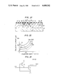
- FIG. 1A is a diagrammatic cross-section of a conventional bipolar transistor.
- FIGS. 1B and 1C are diagrams showing potential distribution along the lines 1B--1B' and 1C--1C' in the bipolar transistor of FIG. 1A.
- FIG. 2A is a diagrammatic cross-section illustrating a semiconductor device according to an embodiment of the present invention.
- FIG. 2B is diagrams showing the potential distribution along the line 2B--2B' in the semiconductor device of FIG. 2A in two operational modes.
- FIGS. 3 and 4 are diagrams of drain current vs. drain voltage characteristic curves achievable by the semiconductor device of FIG. 2A.
- FIGS. 5 to 8 are diagrammatic cross-sections showing structures of the semiconductor device according to embodiments of the present invention.
- FIGS. 9A, 9B and 9C are diagrams showing alternative channel structures of the semiconductor device shown in FIGS. 5 to 8 according to embodiments of the present invention.
- FIGS. 10A and 10B are a diagrammatic cross-section and a circuit diagram of an integrated injection logic (IIL) circuit according to another embodiment of the present invention.
- IIL integrated injection logic
- FIGS. 11, 12 and 13A are circuit diagrams of emitter-coupled logic (ECL) or current mode logic (CML) circuits according to further embodiments of the present invention.
- ECL emitter-coupled logic
- CML current mode logic
- FIG. 13B is a diagrammatic diagram showing an I-V characteristic curve of the constant voltage transistor Q 2 employed in the circuit of FIG. 13A.
- FIGS. 14A and 14B are circuit diagrams showing examples of emitter-follower logic (EFL) circuits of AND gate according to embodiments of the present invention.
- ETL emitter-follower logic
- FIGS. 15A and 15B are circuit diagrams showing non-threshold logic (NTL) circuits of NOR gate according to embodiments of the present invention.
- FIG. 16 is a circuit diagram showing a direct-coupled transistor logic circuit of NOR gate according to an embodiment of the present invention.
- FIGS. 17, 18 and 19 are circuit diagrams showing a resistor transistor logic (RTL) circuit, a diode transistor logic (DTL) circuit and a transistor-transistor logic (TTL) circuit according to embodiments of the present invention.
- RTL resistor transistor logic
- DTL diode transistor logic
- TTL transistor-transistor logic
- FIGS. 20 and 21 are diagrammatic cross-sections of structures of integrated injection logic (IIL) circuits according to further embodiments of the present invention.
- IIL integrated injection logic
- FIG. 22 is a diagram showing I-V characteristic curves of a semiconductor device employed in the circuit of FIGS. 20 and 21.
- FIG. 23 is a circuit diagram of the semiconductor integrated circuit structure shown in FIGS. 20 and 21.
- FIG. 24 is a circuit diagram of NOR and OR gate circuit according to another embodiment of the present invention.
- FIG. 25 is a diagrammatic cross-section of a semiconductor device according to another embodiment of the present invention.
- FIGS. 26 and 27 are circuit diagrams of NOR and OR gate circuits according to embodiments of the present invention.
- FIG. 28 is a circuit diagram of an emitter-follower logic (EFL) circuit according to another embodiment of the present invention.
- ETL emitter-follower logic
- FIG. 29 is a circuit diagram of a non-threshold logic (NTL) circuit according to another embodiment of the present invention.
- FIG. 30 is a circuit diagram showing a static random access memory (RAM) cell according to another embodiment of the present invention.
- FIG. 31A is a circuit diagram showing an IIL inverter circuit according to another embodiment of the present invention.
- FIG. 31B is a diagrammatic cross-section of a semiconductor integrated circuit structure embodying the circuit of the present invention.
- FIG. 32A is a circuit diagram showing an IIL inverter circuit according to another embodiment of the present invention.
- FIG. 32B is a diagrammatic cross-section of a semiconductor integrated circuit structure embodying the circuit of FIG. 32A.
- FIG. 33A is a circuit diagram showing a dynamic random access memory cell according to another embodiment of the present invention.
- FIG. 33B is a diagrammatic cross-section of a semiconductor integrated circuit structure embodying the circuit of FIG. 3A.
- FIG. 34A is a circuit diagram showing a dynamic random access memory (RAM) cell according to another embodiment of the present invention.
- FIG. 34B is a diagrammatic cross-section of a semiconductor integrated circuit structure embodying the circuit of FIG. 34A.
- FIGS. 35 and 36 are diagrammatic cross-sections showing structures of the semiconductor device according to embodiments of the present invention.
- FIG. 37 is a diagram showing I-V characteristic curves of the semiconductor device according to the embodiments shown in FIGS. 35 and 36.
- FIG. 38 is a circuit diagram of NOR gate circuit according to another embodiment of the present invention.
- FIG. 39 is a partial circuit diagram of a general logic circuit including the circuit shown in FIG. 38.
- the static induction transistor may be defined broadly as a field effect transistor having a current path between a carrier injecting region (source) and a carrier extracting region (drain) and a potential barrier for charge carriers which is established in the current path near a controlling electrode and being controllable by a controlling voltage and a drain voltage.
- the static induction transistor may be said to resemble the bipolar transistor in the aspect that a potential barrier exists in the current path.
- a bipolar transistor consists of an emitter, a base and a collector region. The conductivity type of the base region is opposite to that of the emitter and collector regions.
- FIGS. 1A, 1B and 1C diagrammatically illustrate a conventional npn bipolar transistor.
- a bipolar transistor comprises an n type emitter region 1, a p type base region 2 and an n type collector region 3.
- Potential profiles of the bottom of the conduction band along lines 1B--1B' and 1C--1C' are shown in FIGS.
- the top of the valence band (not shown) is parallel to but lower than the bottom of the conduction band approximately by the forbidden gap energy of the semiconductor material.
- the energy of a hole is positive in the downward direction.
- the bottoms of the conduction band in the n type emitter and collector regions are at similar energies (e.g. ⁇ 1 ).
- the base region 2 is of p type, the Fermi energy in the base region 2 is near the top of the valence band, and hence the bottom of the conduction band is raised to a level ⁇ 2 by the built-in potential.
- the base region 2 forms a barrier for the electrons transferred from the emitter 1 to the collector 3.
- a collector current is formed.
- the base region has its own charge carriers (holes in this case) of the opposite conductivity type, they also begin to proceed over the barrier toward the emitter region.
- a base current is allowed to flow.
- the base potential is controlled by the base bias voltage through the base resistance, so that the base potential is basically uniform in the cross-sectional direction when the base current is small. In case the base current becomes large accompanying the significant voltage drop across the base resistance, the base potential tends to shift from the uniform profile and exhibits highest value at the center of the base region in the symmetrical structure. The position of the highest potential barrier shifts from the center in the unsymmetric structure.
- FIG. 2A A fundamental structure of an n-channel static induction transistor according to an embodiment of the present invention is illustrated in FIG. 2A, and the potential profile of the bottom of the conduction band along the line 2B--2B' is illustrated in FIG. 2B for the two operational modes.
- the zero level in FIG. 2B indicates the bottom of the conduction band in a neutral n type region.
- FIG. 2A shows a planar-type structure in which an n - type region 12 is epitaxially grown on an n + type substrate 13 serving as a drain, and an n + type region 11 is diffused or implanted in the surface of the n - type region 12 to form a source region.
- a p + type gate region 14 is formed in the surface of the n - type region 12 by either the ion implantation, the diffusion, or the etching and deposition technique to substantially surround the source region 11 and to define a current channel region.
- the impurity concentration of the current channel region of the n - type region 12 and the gate-to-gate distance i.e.
- the width of the current channel region) W are so selected as to excessively pinch off the current channel region with the depletion layers at zero gate bias as shown in the left-hand diagram of FIG. 2B.
- the bottom of the conduction band is raised by ⁇ at the center of the channel.
- the drain current is controlled mainly by the height of the barrier since the height of the barrier contributes inversely exponentially to the amount of the drain current.
- a positive gate bias is applied, the bottom of the conduction band in the p + type gate region 14 is lowered and approaches the bottom of the conduction band in the channel portion, and hence the depletion layer shrinks to reduce the barrier height.
- the static induction transistor is basically analogous to the conventional field effect transistor in the aspect that the drain current is controlled mainly by the width (i.e. resistance) of the neutral current channel.
- the drain current is controlled mainly by the width (i.e. resistance) of the neutral current channel.
- the drain current will not grow very large under a forward gate bias below a certain value, since a certain forward gate bias is required to reduce the height of the potential barrier.
- the potential profile in the cross-sectional direction is not uniform and is lowest at the center of the channel in the symmetric structure as shown in FIG. 2B. This situation originates from the fact that the channel potential is capacitively controlled by the gate bias voltage. When the structure becomes unsymmetric, the potential minimum point in the cross-sectional direction shifts from the channel center.
- Such positive charge in the n - type channel region 12 will exhibit an attractive force to attract the electrons, although these electrons are less in number than that of the majority carriers injected from the source region in the channel, and may help inducing injection of electrons from the n + type source region 11.
- Both types of carriers are basically drifted by the electric field in contrast to the conventional bipolar transistor.
- the change in the main (drain) current I D with respect to the change in the gate current I G , ⁇ I D / ⁇ I G which corresponds to the current amplification factor ⁇ of the conventional bipolar transistor, is very large according to the present invention, because the channel potential is capacitively controlled by the gate bias voltage in the basic operation.
- the IR voltage drop across the series resistance from the source electrode to the intrinsic gate will become large to act as a negative feedback factor.
- a small barrier between the source region (e.g. n + type) and the channel region (e.g. n - type) ascribed to the difference of the Fermi level in these regions will still remain.
- this device is suitable for the switching operations.
- the device is rendered “off” at a gate bias voltage of about 0 to 0.2 V (volts), and is rendered “on” at a gate bias voltage of about 0.6 V or larger than 0.6 - V.
- the power dissipation of a logic gate according to an embodiment of the present invention is of the order of 0.01 mW.
- the drain regions In semiconductor integrated circuits, it is often preferable to dispose the drain regions on the upper surface because of the easiness of wiring and circuit designing. Furthermore, it should be noted that, when the drain voltage is subjected to changes, the capacitance accompanying the drain region is smaller the better. Thus, an upside-down structure is of interest. Namely, in the structure of FIG. 2A, the n + type region 11 may be used as a drain, and the n + type region 13 as a source. In such upside-down structure, however, the source-to-gate distance naturally changes to the distance between the n + type region 13 and the p + type region 14.
- the thickness of the n - type region below the bottom of the p + type gate region may be reduced (or vanished in some cases).
- the lower edge of the gate region 14 is preferably more sharpened by relying on the selective etching and deposition techniques. The above will hold true also in the following embodiments.
- p-channel devices can be formed by reversing all the conductivity types of the semiconductor regions.
- the use of the characteristics of FIG. 4 is arbitrary, and never is limited to the above example. Also, it will be apparent that the characteristics as shown in FIG. 4 can be varied widely by the selection of the device parameters.
- the device parameters of the silicon transistor structure of FIG. 2A are changed in such a manner that the n - type channel region 12 has an impurity concentration of 1 ⁇ 10 13 cm -3 , a circular cross section of 10 ⁇ m ⁇ (micrometer diameter) and a thickness of 10 ⁇ m and that the gate region 14 has an impurity concentration of 1 ⁇ 10 19 cm -3 , a width of 15 ⁇ m and a depth of 2.5 ⁇ m.
- the drain current is noted to be below 3 ⁇ A, and the current amplification factor ⁇ is about 10.
- FIGS. 5 to 8 show typical examples of the cross-sectional structure of the semiconductor device according to embodiments of the present invention.
- FIG. 5 shows a planar structure of surface gate type similar to that of FIG. 2A.
- the n - type region 12 is formed thick on the side of the n + type drain region 13 to arrange so that the maximum drain voltage to be large.
- the p + type gate region 14 defines a current channel in the n - type current channel region 12.
- the p + type gate region 14 is embedded in the n - type channel region 12. This structure is suitable for making a transistor of a short channel length. By arranging the embedded p + type gate region so as to define a multiplicity of channels, a large output transistor may be formed.
- the p + type gate region 14 is extracted on the surface by a mesa-like structure or by a p + type extracting region extending to the surface.
- p + type gate regions are formed in the recessed portions. Namely, cut-away grooves are formed around the n + type source region 11 and the gate regions 14 are formed in the side wall portion of the cut-aways. The bottom portions of the cut-aways are covered with a thick insulator (e.g.
- gate electrodes 24 are formed thereon.
- the p + type gate region 14 touches the gate electrode 24 on the side surface.
- This structure is suitable for minimizing the gate capacitance and increasing the current gain, although the manufacture thereof is not simple.
- the space above the gate electrode 24 is filled with an insulating material such as polyimid resin, silicon oxide, polycrystalline silicon of high resistivity, and so forth.
- FIG. 8 shows a lateral structure in which the current channel region is defined by the p + type upper gate region 14 and the p + type lower gate region 14'.
- the lower gate region 14' may be electrically connected to the upper source region 11 or set at a constant voltage.
- This structure is easy to manufacture although the surface occupation area will become large.
- the channel width and the impurity concentration in the channel are chosen so as that there appears a potential barrier in the channel due to the gate to channel built-in voltage.
- the drain current is allowed to flow by applying a gate bias voltage in a forward direction.
- p-channel devices may be formed simply by reversing all the conductivity types.
- the source and the drain regions may be exchanged to form upside-down (or inversely operated) structures as mentioned before.
- the current channel region is so designed that it becomes completely pinched off at zero gate bias voltage.
- Alternative structures may be found in the co-pending U.S. patent applications mentioned before.
- the channel width W and the impurity concentration in the region of high resistivity are important in the present invention.
- the term “just pinched-off” will be used to express the state that the channel is just pinched off by the depletion layers, i.e. the depletion layers growing from both sides of the channel just touch each other.
- the term “over pinch-off” will be used to express the state that the depletion layers growing from both sides of the channel overlap each other, and that a potential barrier is established for all the charge carriers moving from the source to the drain.
- the channel is over pinched off at zero gate bias through the selection of the channel width W and the impurity concentration in the channel region.
- the channel width is preferably not wider than about 6 ⁇ m, about 20 ⁇ m and about 60 ⁇ m, respectively. More preferably, the channel width W is so selected that the depletion layer (of width d 0 ) from each side touches the other side of the channel (W ⁇ d 0 ) at zero bias.
- the potential barrier will have a height (at the central portion) above about one quarter of the built-in potential.
- the main current of the static induction transistor (SIT) in its "off" state is reduced less than at least one tenth of that of the just pinched-off static induction transistor.
- the channel width When the channel width is excessively narrowed, the resistance of the channel in the "on” state will become large. Therefore, there is a limit in narrowing the channel.
- the channel From the viewpoint of low "on” resistance, meaning a low channel resistance when the transistor is turned “on”, the channel preferably has a large width.
- the impurity concentration in the channel region is preferably as low as possible provided that the manufacture thereof can be done stably and preferably at a low cost.
- the gate region preferably has a high impurity concentration from the viewpoint of low gate spreading-resistance. A higher impurity concentration of the gate region will accompany a higher built-in potential between the gate and the channel. Furthermore, the gate region preferably has a thin width for decreasing the parasitic gate capacitance and the gate current. A decrease in the gate capacitance will lead to an improvement in high speed operation. Furthermore, when the gate voltage is sufficiently high in the forward direction, there is the possibility that a current flows between the source and the gate. Considering this fact, the channel region preferably has a larger cross section in comparison with the area of the gate region exposed to the source region.
- the current amplification factor ⁇ exceeds unity when the gate area is one hundred times broader than that of the channel region in an upside-down structure. This ratio can be used as an estimate for the critical value.
- the minority carriers injected from the gate region, if any, are diffused to reach the source region.
- the possibility of recombination in the channel region of a low impurity concentration is very small.
- the impurity concentration in the gate region and/or that in the channel region may be graded.
- FIGS. 9A to 9C show embodiments of the channel structure following the embedded gate structure of FIG. 6.
- n - type region 12 covers most of the surfaces of the p + type gate region. Because of the presence of the high resistivity regions, both the junction capacitance between the source and the gate and the capacitance between the gate and the drain are small.
- the n - type region 12 of a high resistivity is formed to an intermediate height of the p + type gate region 14, and another region 15 of a relatively low resistivity is grown thereon.
- the source-to-intrinsic gate resistance becomes small, the maximum drain voltage may be high and the gate-to-drain capacitance can be reduced.
- the region 15 of the lower resistivity may be formed so as not to touch the gate region, but to be separated therefrom by a thin n - type region of a high resistivity.
- the n + type source region may be projected into the channel between the gate regions to lower the series resistance. Similar arrangement may be adopted also on the drain side.
- FIG. 9C shows another structure in which the current channel region 12 of a high resistivity is formed only in a limited thin region surrounded by the gate regions 14. Regions 15 and 16 sandwiching the channel region 12 and the gate region 14 therebetween may have the same resistivity or different resistivities.
- the whole source-to-drain "on" resistance meaning when such resistance when the transistor is turned on
- the leak current when the transistor is turned off can be arranged to be very small.
- the impurity concentration in each region may be arranged to have a gradient. In an extreme case, there may be no boundary of regions. Also, the selection of the impurity concentration may be changed widely to meet the aimed use.
- the channel region of a low impurity concentration may also be formed with an intrinsic region. In these embodiments, the channel width and the impurity concentration in the channel are chosen so as to establish the potential barrier in the channel at zero gate bias voltage.
- FIGS. 10A and 10B shown an SIT IIL structure and a circuit diagram thereof, respectively.
- a bipolar injector transistor T 2 serves as a constant current source and supplies a current to an input terminal 24 (when it is at low voltage) or to the gate of a static induction transistor T 1 .
- the driver transistor of the preceding stage is turned off, the carriers are injected to the gate of the static induction transistor T 1 and raise the gate potential.
- the driver transistor T 1 of this stage is turned on and the output terminal is connected to a low voltage.
- an output terminal 23 provides an inverted output.
- the injector (or load) transistor T 2 is formed with a lateral bipolar transistor including a p + type emitter region 18, an n - type base region 12' and a p + type collector region 14, and the driver (or inverter) transistor T 1 is formed with an upside-down static induction transistor including an n + type source region 11, an n.sup. - type channel region 12, an n + type drain region 13 and a p + type gate region 14.
- the gate region 14 which is a region common with the collector region of the bipolar transistor T 2 surrounds the channel region 12 to define the current channel region. Also, the gate region 14 is formed deep into the n - type region 12 so as to reduce the source-gate distance since this static induction transistor is the upside-down type.
- Electrodes 28, 24, 21 and 23 are formed on the regions 18, 14, 11 and 13, respectively.
- the carriers (holes) are directed to the collector region 14 and stored therein.
- the gate potential rises to turn the n-channel static induction transistor T 1 on.
- holes may be injected from the p + type gate region into the n - type channel region.
- the positive charge in the channel region 12 helps inducing the injection of electrons from the source region 11.
- the channel resistance is reduced to provide a large drain current with a small supply voltage.
- the static induction transistor T 1 may work as a current sink to reduce the change in amount of the carrier injected through the injector transistor T 2 .
- this SIT IIL structure provides a high speed operation together with a small gate capacitance.
- the injector transistor mostly serves as a constant current source, it may be formed with any type of transistor, i.e. bipolar transistor, junction field effect transistor, insulated-gate field effect transistor or a static induction transistor.
- the static induction transistor (SIT) according to the present invention can perform a high speed operation at a low power dissipation, using a forward gate bias, and can substitute even a part of a conventional bipolar transistor circuit.
- SIT-IC static induction transistor integrated circuits
- FIG. 11 shows an emitter-coupled logic (ECL) or current mode logic (CML).
- ECL emitter-coupled logic
- CML current mode logic
- NOR and OR logic signals are amplified (impedance transformation) in the output SIT's QO 1 and QO 2 to provide low impedance outputs.
- the reference SIT QR is supplied with a constant reference voltage supplied from a reference voltage circuit V ref CKT in which a bipolar transistor is connected with a resistor to generate a constant voltage at point R. Diodes D are used for the temperature compensation. Similar reference voltage circuits are used also in the following embodiments. The SIT of the present invention is obviously used in the reference voltage circuit.
- the operation speed is influenced by the accompanying capacitance which is being subjected to charging and discharging.
- all the drain, gate and source regions of the input and reference SIT's QA, QB and QR are subjected to voltage change.
- the operation speed is limited.
- the number of regions which are subjected to voltage changes as well as the area of such regions are preferably reduced.
- FIG. 12 shows a modification in which the drains of the input SIT's QA and QB are directly connected to the constant supply voltage V cc , and an intermediate SIT QI is used.
- the input SIT's QA and QB generate an OR signal at their sources, and the intermediate SIT QI inverts this OR signal into a NOR signal.
- the output SIT's QO 1 and QO 2 perform impedance transformation.
- a resistor R 5 is used as a load for the input SIT's.
- the load resistor R 5 may be replaced by a parallel connection of a resistor R 10 and an SIT Q 2 , which provides a constant voltage characteristic of FIG. 13B, as shown in FIG. 13A.
- a current limiting field effect transistor may be connected in series to the input SIT's.
- FIGS. 14A and 14B show emitter-follower logic (EFL) circuits of a 3-input AND gate.
- Three p-channel input SIT's are connected in parallel and an n-channel multi-drain SIT is connected in a source-follower arrangement.
- the load for the input SIT's may be a resistor R 1 (FIG. 14A), or a parallel connection of a constant voltage SIT Q 3 and a resistor R 11 (FIG. 14B).
- input SIT's QA, QB and QC are normally "on", so that the source voltage becomes high only when all the inputs A, B and C are at a high level and all the input SIT's QA, QB and QC are cut off.
- FIG. 15A shows an non-threshold logic (NTL) circuit, wherein input SIT's QA and QB are connected in parallel to each other and in series to a load resistor R 1 .
- a capacitor C short-circuits the ac component at the source of the input SIT's to the ground.
- FIG. 15B shows a modification of non-threshold logic circuit, wherein the load resistor R 1 in FIG.
- FIGS. 15A and 15B the NOR signal is provided at the common drain region of the input SIT's QA and QB, respectively.
- FIG. 16 shows a 3-input NOR logic circuit wherein three input SIT's QA, QB and QC are connected in parallel to each other and in series to the parallel connection of a constant voltage type SIT Q 4 and a resistor R 12 .
- FIG. 17 shows a 3-input resistor transistor logic (RTL) circuit forming a NOR gate, wherein three input signals A, B and C are applied to input SIT's QA, QB and QC through resistors RA, RB and RC, respectively.
- the RTL circuit has the disadvantage that the operation speed is reduced by the input resistors.
- FIG. 18 shows a diode transistor logic (DTL) circuit, wherein three inputs A, B and C are applied through normally "on" diodes DA, DB and DC to supply an AND signal at their common anode.
- An SIT QD is used to invert the AND signal and to supply an amplified NAND signal.
- FIG. 19 shows a transistor-transistor logic (TTL) circuit, wherein three inputs are given to a normally "on" 3-fan-in SIT QI to provide an AND signal at the common source.
- the AND signal is inverted and amplified through SIT's Q 1 to Q 4 to supply a NAND signal.
- the static induction transistor having a current channel which is over pinched-off at zero gate bias provides a high speed operation, and can substitute a bipolar transistor without requiring a drastic change of the circuit design. Furthermore, such substitution can be done only in part of a total system.
- the base region 2 when the base region 2 is formed with, for example, a thin p type region of a low impurity concentration, depletion layers will grow from the junctions which are formed with n + type emitter and collector regions 1 and 3 to reduce the effective base region of the flat potential portion. Where the potential profile of the band extrema shows gradient, free charge carriers will flow out to the lower energy portion to leave no free charge carriers, and only the ionized impurity atoms remain. When there remains almost no flat band portion (i.e. neutral region) in the base region, the base region is pinched off, and will serve as a potential barrier for those electrons moving from the emitter region. Such a depleted base region tends to loose the character of resistive control.
- a flat band portion i.e. neutral region
- the height of the potential barrier can be controlled fundamentally capacitively by the base and collector voltages.
- the punch-through bipolar transistor there exists the built-in voltage between the p + region and the p region, so that the potential profile in the cross-sectional direction of the base region shifts from the uniform profile and exhibits minimum valve at the center of the channel in the symmetric structure.
- the collector current will increase with an increase in the collector voltage.
- the punch-through bipolar transistor resembles the static induction transistor described in this specification in this aspect of the presence of a capacitively controllable barrier height at zero base and drain voltages.
- the barrier height can, in most cases, be above about one half of the forbidden gap at zero base and collector voltages to provide wider dynamic range than that of the static induction transistor, but the ionized impurity atoms in the base region have the same polarity as that of the carriers to be injected from the emitter region.
- the punch-through bipolar transistor may provide a performance which is somewhat inferior to that of the static induction transistor, but it can be used as a good substitute of the static induction transistor. Since the base region is substantially pinched off (depleted), the charge carriers are drifted by the electric field which is established therein, and the storage of minority carrier is very small, to provide a good high frequency performance and a high speed operation.
- the gate capacitance is very small due to the substantially pinched-off and thin base region, the power dissipation is reduced further and the operation speed is enhanced.
- the punch-through bipolar transistor there exists substantially or completely depleted base region having an opposite conductivity type compared to the emitter and the collector region, so that there easily appears a high potential barrier in the channel compared to that in the channel of the SIT of the present invention described previously.
- the channel length i.e., the emitter to collector distance, can be reduced compared to the SIT described previously where the potential barrier height holds at the same value.
- FIGS. 20 and 21 show IIL circuit structures including the punch-through bipolar transistor according to embodiments of the present invention. Namely, in the structure of a vertical type upside-down static induction transistors, a thin p type region interrupts an n type channel adjacent to a drain region (FIG. 20) and in the midway of this channel (FIG. 21).
- an n - type region 32 is formed on an n + type region 31.
- a lateral bipolar transistor is formed by the n - type region 32 and the p type regions 34 and 36.
- the p type region 36 serves as an emitter of the injector transistor, and the p + type region 34 serves both as a collector of the injector transistor and as the gate region of the originally intended driver SIT.
- a thin p type layer 34' connects the p + type regions 34, and separates the n type current path into the source (emitter) part and the drain (collector) part.
- This bipolar transistor of the upside-down type is formed with an n + type emitter region 31, an n - type region 32, a thin p type base region 34' and an n + type collector region 33 with or without intervening an n - type region 35 between the p type region 34' and the n + type collector region 33.
- the thick p + type region 34 which is contiguous to the thin p type region 34' will be referred to as a gate region.
- Electrodes 46, 44 and 43 are formed on the regions 36, 34 and 33 to serve as the emitter and collector electrodes of the injector transistor and as the collector electrode of the driver transistor, respectively.
- An insulating film 47 covers the other surfaces than the metal contact area.
- the base region 34' is thin and has a low impurity concentration, so that it is substantially depleted with the depletion layers which grow by the built-in potential alone which exists between the emitter and the base regions and between the base and the collector regions.
- p type regions 34' may be formed by redistributing p type impurities from the p + type region 34. Then, the impurity concentration and the thickness of the p type region 34' will decrease as it goes toward the center.
- the height of the potential barrier formed at the p type regions 34' is the smallest at the central portion due to the fundamental character of capacitive control and possibly to a graded impurity concentration as described above.
- similar performance to that of the static induction transistor is expected in the punch-through bipolar transistors of these embodiments, and practically is found to exist. It is proved that the punch-through bipolar transistor may be positively manufactured as a substitute of the static induction transistor.
- the base region has an excessively small thickness and an excessively low impurity concentration, the energy positions of the band extrema in the base region become almost the same as those of the emitter and the collector regions. In such case, no potential barrier is present practically, and the transistor will loose the controlling ability of the main current which is to be controlled by a controlling voltage.
- the "substantially pinched-off base region” is herein defined as a base region mostly depleted but having Fermi level different from that of the emitter region, so that the base region establishes a potential barrier for the charge carriers flowing from the emitter to the collector, and that the height of the potential barrier is fundamentally capacitively controllable by the gate and the collector voltages.
- the effective base region neutral base region
- the carrier storage effect is a small particularly narrow p region structure, and a very high operation speed is provided.
- Carriers flowing from the emitter to the collector pass over the potential barrier formed by the depleted base region, and are injected to the collector side and are drifted by an electric field established by the collector voltage. There appears almost no effect of storage of minority carriers.
- the base bias is set to be sufficiently forward, minority carriers can be injected from the gate region 34 to the emitter region 33 through the base region 34'.
- the base region 34' will possess the property of a usual base region of the bipolar transistor.
- the gate region 34 may be formed thick and it may be heavily doped, so that the resistance of the region 34 is negligible.
- FIG. 22 A measured example of the current versus voltage characteristics of a punch-through bipolar transistor which can be used in the embodiments of the present invention is shown in FIG. 22. It is considered that the base region is not yet completely depleted only by the built-in potential, since the region C shows bipolar-like characteristics. However, as the base bias voltage and/or the drain voltage become more forward, the drain current will increase to exhibit non-saturating characteristics as shown in the region D, indicating that the base region becomes depleted and the barrier height is gradually pulled down by an increase in the drain voltage. A decrease in the barrier height leads to an increase in the collector current.
- the region C can be controlled to be either wide or narrow (or null) by controlling the degree of depletion of the base region.
- the collector current When charge carriers from the emitter region diffuse into the base region, the collector current will follow an exponential law in a small drain voltage region. If the resistance influences the carrier transport, a resistive characteristic may appear also.
- the base region is perfectly depleted only by the built-in potential, the application of a collector voltage will immediately lower the potential barrier, so that the collector current easily becomes large.
- the base region potential is basically capacitatively controlled by the gate bias voltage, so that the potential barrier is usually lowest at the center of the channel.
- the punch-through bipolar transistor can be used in the same mode as that of the conventional bipolar transistor. Namely, the collector current can be controlled by the forward base bias voltage as well as by the collector voltage.
- the thickness of the barrier layer should be determined, by considering the desired output current. When a large load current is required, e.g. for driving a TTL gate, the barrier layer should be formed sufficiently thin and at a site sufficiently near the emitter region.
- FIG. 23 shows a circuit diagram of the IIL circuit structures of FIGS. 20 and 21, comprising the punch-through driver transistor T 1 and a lateral bipolar injector transistor T 2 .
- Structure of the integrated semiconductor device can be altered or modified according to the usual knowledge and the preceding description.
- the injector transistor T 2 may be replaced by a usual field effect transistor, a static induction transistor, or a punch-through transistor. Also, it is possible to form the injector transistor T 2 by the punch-through transistor, and the driver transistor T 1 by a static induction transistor.
- FIG. 24 shows a NOR-OR circuit comprising three IIL units. Two inputs are applied to two IIL units, respectively. A pair of outputs of the two input IIL units are combined to supply an NOR output, while another pair of similar outputs of the two IIL units are supplied to an output IIL unit to generate an inverted NOR signal, i.e. an OR signal, at the drain of the output driver transistor TO 1 .
- an inverted NOR signal i.e. an OR signal
- FIG. 25 shows an example of a punch-through transistor having a substantially or completely depleted base region which, in turn, forms a thin potential barrier layer for the carriers in the emitter region.
- a punch-through transistor having a substantially or completely depleted base region which, in turn, forms a thin potential barrier layer for the carriers in the emitter region.
- On a p type substrate there are formed an n + type region 55 and also an n type region 54 both serving as a collector region.
- a p type base region 52 is surrounded by a p + type control electrode region 53.
- An n + type emitter region 51 is formed in the p type base region 52.
- An n + type region 55' for extracting collector electrode is formed from the surface to the n + type collector region 55.
- An emitter electrode is formed with a doped polycrystalline silicon region 51' and a metal film 58 is formed thereon.
- a base electrode 59 and a collector electrode 60 are formed of metal films.
- the transistor is isolated, by cut-away grooves in the sideway and also by the pn junction, from the substrate.
- the surfaces of the semiconductor body excepting the electrode contacting area are covered with a passivation film 56, for example formed with silicon oxide, silicon nitride, aluminium oxide or the combinations thereof.
- the cut-away or recessed grooves are filled with an insulating material, for example of an oxide region, a high resistivity polycrystalline silicon or insulating resin such as polyimid.
- the impurity concentration of the n + type emitter region 51 is of the order of 10 18 to 10 21 cm -3
- that of the p type base region 52 is of the order of 10 12 to 10 16 cm -3
- that of the n type collector region is of the order of 10 14 to 10 17 cm -3
- that of the base electrode-extracting p + type region 53 is of the order of 10 16 to 10 21 cm -3
- that of the n + type collector region 55 is of the order of 10 17 to 10 20 cm -3 .
- the thickness and the impurity concentration of the p type base region 52 is so selected that the base region 52 can be substantially or completely pinched off by the built-in potentials on both sides.
- the isolating recessed grooves may have any shape of their cross sections.
- a pnp transistor can be formed by simply reversing all of the conductivity types. Only the required condition of designing is that the base region is substantially or completely depleted and that it leaves a thin potential barrier layer in the current path in a main operative region of the transistor.
- the punch-through transistor having this feature has the advantages that the minority carrier storage effect can be reduced very small and that the base capacitance (both the emitter-base and the base-collector capacitances) can be reduced greatly. These advantages provide a very high speed operation, and furthermore they can be exhibited remarkably when used in an integrated circuits. All the currently existing bipolar integrated circuit techniques, such as ECL, EFL, NTL, DTL, RTL, TTL, static RAM, dynamic RAM, and ROM, can be directly applied so as to use the punch-through transistors described above. Detailed description of embodiments of typical types of the integrated semiconductor circuits will be described hereinbelow.
- FIG. 26 shows an emitter-coupled logic (ECL) circuit according to an embodiment of the present invention.
- ECL emitter-coupled logic
- FIG. 27 shows another emitter-coupled logic (ECL) circuit according to another embodiment of the present invention.
- Collectors of the input transistors QA and QB are directly connected to the supply voltage line V cc , hence the voltage change of these collector regions is eliminated, and the influence of the capacitances accompanying these regions are eliminated, thereby providing an improved high-speed operation of the circuit as compared with the device of FIG. 26.
- FIG. 28 shows an emitter-follower logic (EFL) circuit according to an embodiment of the present invention.
- ENL emitter-follower logic
- Three inputs A, B and C are applied through bipolar transistors. QA, QB and QC, respectively, and AND logic outputs are given through a multi-source output bipolar transistor QO.
- bipolar transistors of both the pnp and the npn types are mixedly used to form a 3-input AND gate.
- This embodiment is composed of a rather small number of semiconductor elements and a large number of electrodes are connected to constant voltage supplies. Therefore, power dissipation is small, and an enhanced high-speed operation is provided. Furthermore, the integration density can be greatly improved.
- the resistor R 1 can be effectively replaced by a parallel connection of a resistor and a constant voltage device such as a static induction transistor as described before.
- FIG. 29 shows a non-threshold logic (NTL) circuit according to an embodiment of the present invention, wherein two inputs A and B are applied to input transistors QA and QB of the punch-through type to provide a NOR logic output. Furthermore, since the minority carrier storage in the base region is negligibly small, the capacitor C can be dispensed with. Furthermore, as mentioned above, resistors R 1 and R 4 can be effectively replaced by constant voltage circuitries as shown in FIG. 15B.
- NTL non-threshold logic
- FIG. 30 shows a static random access memory composed of punch-through bipolar transistors according to an embodiment of the present invention.
- Transistors T 11 and T 12 are connected to the address lines and to the read and write lines through the emitters.
- the bipolar transistor having a substantially or completely depleted base region on one hand, can be used as a substitute of a usual bipolar transistor, and on the other hand, as a substitute of a static induction transistor of the forward gate bias type.
- all the circuits utilizing these transistors can be formed with such bipolar transistors, while maintaining the advantages of both types.
- FIGS. 31A and 31B show an IIL inverter circuit diagram and a diagrammatic cross-sectional view of a semiconductor integrated circuit structure embodying this circuit according to an embodiment of the present invention.
- a metal-oxide-semiconductor field effect transistor (MOS FET) is used as an injector transistor T 2 , and a bipolar transistor of punch-through type is used as a drive transistor T 1 .
- the number of output terminals can be increased practically arbitrarily.
- the injector transistor T 2 is not limited to an enhancement mode FET but it may be depression mode FET or a bipolar transistor. In FIG.
- the injector transistor T 2 is formed with a p + type source region 66, an n - type region 62, a p + type drain region, and a common gatedrain electrode 68, whereas a driver transistor is formed with an n + type emitter region 61, an n - type emitter region, a thin p type base region 73, a p + type gate region 64, an n - type collector region 65', an n + type collector region 65 and a collector electrode 67.
- the base region 63 may be formed close or adjacent to the emitter region 61 to provide a large output current. In such a case, the p + type gate region 64 may be indented to lower the emitter-base capacitance.
- FIGS. 32A and 32B show another ITL inverter circuit, and a diagrammatic cross-section of a semiconductor integrated circuit embodying this circuit according to another embodiment of the present invention, wherein a MOS SIT is used as the injector transistor T 2 , and a bipolar transistor of the punch-through type is used as the driver transistor T 1 .
- the structure of FIG. 32B is almost similar to that of FIG. 31B.
- reference numeral 69 indicates the channel region provided with a metal-oxide-semiconductor gate.
- various combinations of IIL circuits provide various types of logic circuits capable of providing high speed switching operations at low power dissipation.
- FIGS. 33A and 33B show a dynamic random access memory cell circuit diagram using bipolar transistor of the punch-through type according to the present invention and a diagrammatic cross-section of a semiconductor integrated circuit structure embodying this circuit according to an embodiment of the present invention.
- Word lines or address lines are indicated by 71 and 72, and a bit line or data line is indicated by 73.
- a lateral pnp type transistor T 15 comprises a p + type region 71, an n - type region 75 and a p type region 74, which form the emitter, the base and the collector, respectively.
- an npn type transistor T 16 is composed of an emitter region 72, a base region 74 and a collector region 73.
- the p + type region 71 and the n + type region 72 form the word lines or address lines.
- the n + type region 73 represents the bit line or the data line. Electric charge is stored in a capacitor formed between the base and the collector of the transistor T 16 .
- This structure can be applied to form a matrix of a desired number of units so as to compose a dynamic random access memory.
- the p type region 74 between the n + type region 72 and the n + type region 73 is in the state of about being pinched off at zero gate bias. It is obvious that the pair of the n + type region 73 and the p type region 74 as well as the pair of the n + type region 72 and the p type region 74 are not necessarily disposed contiguous to each other.
- FIGS. 34A and 34B show a dynamic random access memory (RAM) cell circuit and a corresponding cross-section of a semiconductor integrated circuit structure, respectively, according to the present invention.
- a dynamic RAM cell can be composed of a bipolar transistor which has a perfectly depleted base region. When the base region is perfectly depleted, the "on-off" control of the transistor can be accomplished by varying capacitively the height of the potential barrier without such need to let an electric current to flow through the base region as noted in conventional bipolar transistors.
- Reference numeral 81 indicates a bipolar transistor of the punch-through type
- numeral 82 in FIG. 34A represents a capacitor formed with the p type region 86, the p + type region 87 and the n 30 type region 85 shown in FIG. 34B.
- the word line or address line is indicated by reference numeral 83, and the bit line or data line is represented by numeral 84.
- the base region of the bipolar transistor 86 is completely pinched off, and the potential barrier is controlled by the base voltage, i.e. the word line signal, to accomplish the "on-off" control of the transistor, and hence to accomplish read and write operations of the memory cell.
- the above-mentioned structure can be applied as well to a three-transistor dynamic random access memory cell structure, a four-transistor dynamic random access memory cell structure and to a six-transistor static random access memory cell structure (disclosed in my pending Japanese Patent Application No. 52-4633). It is also possible to compose a read-only memory, in which data are written in an insulating film during the mask pattern process. It is also possible to form a shift registor by the cells of this embodiment (disclosed in my pending Japanese Patent Application No. 52-4633).
- the memory cells shown in FIGS. 33A, 33B, 34A and 34B can provide high-speed read and write operations at a low power dissipation.
- FIG. 35 shows an almost constant voltage device of a planar structure according to an embodiment of the present invention.
- the bipolar transistor aimed to serve as a constant voltage device is controllable by a base voltage.
- This constant voltage device is similar to the constant voltage static induction transistor, in which the current change can cause practically no change in the output voltage (disclosed in my pending Japanese Patent Application filed on Feb. 7, 1977, entitled "Integrated semiconductor device”).
- the emitter is formed in the neighborhood of the collector, and thus the series resistance and the collector resistance are small. Thereby, the collector voltage can easily control the potential barrier, and thus a constant voltage device can be composed.
- the p type region 90 is formed between the emitter region 84 and the collector region 85 and is completely depleted, thereby the potential barrier is reduced immediately after the application of a collector voltage. Amount of current flow can also be controlled by the length of the region 90 extending in the direction perpendicular to the surface of the sheet of drawing.
- Recommended impurity concentrations are as follows: about 10 18 -10 ⁇ cm -3 in the n + type regions 84, 85 and 95; about 10 16 -10 21 cm -3 in the p + type region 83; about 10 13 -10 17 cm -3 in the n type region 91; and about 10 13 -10 17 cm -3 in the p type region 90. Apparently, these values can be varied also according to the intended use and to the available manufacturing technique.
- FIG. 36 shows another structure of an almost constant voltage device of a lateral structure according to an embodiment of the present invention. Description made in connection with FIG. 35 can be applied also to this embodiment.
- the impurity concentration of an n - type region 92 is about 10 12 to 10 15 cm -3 .
- the thickness of the p type region 90 may be arranged to be thin for the purpose of providing a good characteristic of a constant voltage device.
- FIG. 37 shows characteristic curves of the collector current ( ⁇ A) vs. collector voltage (V) representing a performance of an example of the constant voltage device according to the embodiments mentioned above.
- the voltage level can be precisely controlled without being influenced by the number of transistors connected to the input gate (i.e. the number of the fan-in). Therefore, the above-mentioned constant voltage transistors can be used advantageously in logic gate structures, as described previously in connection with the static induction transistor IC.
- FIG. 38 shows an NOR gate circuit with three inputs according to an embodiment of the present invention.
- the supply voltage is applied through a parallel connection of a bipolar transistor T 18 and a resistor R 30 .
- the output voltage level is hardly influenced by the number of the inputs. This means that the NOR logic output voltage level in case of the arrival of one "1" input signal does not differ from that in case of the arrival of three "1" input signals.
- FIG. 39 shows part of a general logic circuit according to an embodiment of the present invention.
- Three inputs A, B and C are applied to three input transistors QA, QB and QC, respectively, to provide an NOR signal at the common drain.
- This NOR signal is directly supplied to the subsequent stage on the one hand, and is inverted through an inverter transistor QO into an OR signal on the other hand.
- the use of this OR signal can be arbitrarily determined.
- the thin base region of the punch-through bipolar transistor may be connected directly to a metal electrode (i.e. Schottkey electrode), or to a metal electrode through an insulating film (MIS electrode).
- a metal electrode i.e. Schottkey electrode
- MIS electrode insulating film
- the transistors of both the SIT type and the punch-through type according to the present invention both can provide a high-speed operation while they can serve as a substitute of bipolar transistors even in part of an entire system.
- the conventional circuit technique of the bipolar transistor can be directly utilized to form higher-speed integrated circuits utilizing those transistors according to the present invention.
- the semiconductor material used in the present invention may be selected from silicon, germanium, III-V compounds and other semiconductor materials. For example, gallium arsenide and other wide band gap semiconductors are suitable for providing a higher barrier hieght, i.e. a wider dynamic range.
- the transistors and the IC's according to the present invention can be manufactured by utilizing the conventional manufacturing techniques.
- the ion implanation techniques can be advantageously utilized.
Landscapes
- Engineering & Computer Science (AREA)
- Physics & Mathematics (AREA)
- Condensed Matter Physics & Semiconductors (AREA)
- General Physics & Mathematics (AREA)
- Manufacturing & Machinery (AREA)
- Computer Hardware Design (AREA)
- Microelectronics & Electronic Packaging (AREA)
- Power Engineering (AREA)
- Chemical & Material Sciences (AREA)
- Crystallography & Structural Chemistry (AREA)
- Junction Field-Effect Transistors (AREA)
Applications Claiming Priority (8)
| Application Number | Priority Date | Filing Date | Title |
|---|---|---|---|
| JP1046077A JPS5396681A (en) | 1977-02-02 | 1977-02-02 | Semiconductor ic |
| JP52-10460 | 1977-02-02 | ||
| JP52015880A JPS5853517B2 (ja) | 1977-02-15 | 1977-02-15 | 半導体集積回路 |
| JP52-15880 | 1977-02-15 | ||
| JP52-17327 | 1977-02-18 | ||
| JP1732777A JPS53102661A (en) | 1977-02-18 | 1977-02-18 | Semiconductor ic |
| JP52019466A JPS5924549B2 (ja) | 1977-02-24 | 1977-02-24 | 半導体論理集積回路 |
| JP52-19466 | 1977-02-24 |
Related Parent Applications (1)
| Application Number | Title | Priority Date | Filing Date |
|---|---|---|---|
| US06220122 Continuation | 1980-12-24 |
Publications (1)
| Publication Number | Publication Date |
|---|---|
| US4608582A true US4608582A (en) | 1986-08-26 |
Family
ID=27455395
Family Applications (1)
| Application Number | Title | Priority Date | Filing Date |
|---|---|---|---|
| US06/515,462 Expired - Lifetime US4608582A (en) | 1977-02-02 | 1983-07-20 | Semiconductor device having non-saturating I-V characteristics and integrated circuit structure including same |
Country Status (5)
| Country | Link |
|---|---|
| US (1) | US4608582A (nl) |
| DE (1) | DE2804500C2 (nl) |
| FR (1) | FR2379913A1 (nl) |
| GB (1) | GB1600825A (nl) |
| NL (1) | NL191525C (nl) |
Cited By (7)
| Publication number | Priority date | Publication date | Assignee | Title |
|---|---|---|---|---|
| US4945392A (en) * | 1987-04-28 | 1990-07-31 | Olympus Optical Co., Ltd. | Static induction transistor and manufacturing method of the same |
| US5066603A (en) * | 1989-09-06 | 1991-11-19 | Gte Laboratories Incorporated | Method of manufacturing static induction transistors |
| US5126830A (en) * | 1989-10-31 | 1992-06-30 | General Electric Company | Cryogenic semiconductor power devices |
| US5283428A (en) * | 1990-11-27 | 1994-02-01 | Canon Kabushiki Kaisha | Photoelectric converting device and information processing apparatus employing the same |
| US5391897A (en) * | 1992-09-16 | 1995-02-21 | Honda Giken Kogyo Kabushiki Kaisha | Status induction semiconductor device |
| US6262466B1 (en) | 1994-07-06 | 2001-07-17 | Robert Bosch Gmbh | Lateral semiconductor structure for forming a temperature-compensated voltage limitation |
| CN111505087A (zh) * | 2014-12-18 | 2020-08-07 | 生命科技公司 | 使用大规模 fet 阵列测量分析物的方法和装置 |
Families Citing this family (5)
| Publication number | Priority date | Publication date | Assignee | Title |
|---|---|---|---|---|
| DE2820913A1 (de) * | 1977-05-15 | 1978-11-23 | Zaidan Hojin Handotai Kenkyu | Integrierte halbleitervorrichtung |
| FR2480505A1 (fr) * | 1980-04-14 | 1981-10-16 | Thomson Csf | Transistor a effet de champ a jonction de puissance a fonctionnement vertical et procede de fabrication |
| JPS59119848A (ja) * | 1982-12-27 | 1984-07-11 | Fujitsu Ltd | 半導体装置の製造方法 |
| IT1213171B (it) * | 1984-05-21 | 1989-12-14 | Ates Componenti Elettron | Transistore bipolare di potenza. |
| FR2969815B1 (fr) * | 2010-12-27 | 2013-11-22 | Soitec Silicon On Insulator Tech | Procédé de fabrication d'un dispositif semi-conducteur |
Citations (3)
| Publication number | Priority date | Publication date | Assignee | Title |
|---|---|---|---|---|
| US29971A (en) * | 1860-09-11 | Cotton-cleaner | ||
| US3808515A (en) * | 1972-11-03 | 1974-04-30 | Bell Telephone Labor Inc | Chopper devices and circuits |
| US4115797A (en) * | 1976-10-04 | 1978-09-19 | Fairchild Camera And Instrument Corporation | Integrated injection logic with heavily doped injector base self-aligned with injector emitter and collector |
Family Cites Families (5)
| Publication number | Priority date | Publication date | Assignee | Title |
|---|---|---|---|---|
| US3409812A (en) * | 1965-11-12 | 1968-11-05 | Hughes Aircraft Co | Space-charge-limited current triode device |
| JPS526076B1 (nl) * | 1971-04-28 | 1977-02-18 | ||
| JPS5217720B1 (nl) * | 1971-07-31 | 1977-05-17 | ||
| JPS5811102B2 (ja) | 1975-12-09 | 1983-03-01 | ザイダンホウジン ハンドウタイケンキユウシンコウカイ | 半導体集積回路 |
| JPS608628B2 (ja) | 1976-07-05 | 1985-03-04 | ヤマハ株式会社 | 半導体集積回路装置 |
-
1978
- 1978-01-31 NL NL7801082A patent/NL191525C/nl not_active IP Right Cessation
- 1978-02-01 GB GB4100/78A patent/GB1600825A/en not_active Expired
- 1978-02-02 DE DE2804500A patent/DE2804500C2/de not_active Expired - Lifetime
- 1978-02-02 FR FR7802938A patent/FR2379913A1/fr active Granted
-
1983
- 1983-07-20 US US06/515,462 patent/US4608582A/en not_active Expired - Lifetime
Patent Citations (3)
| Publication number | Priority date | Publication date | Assignee | Title |
|---|---|---|---|---|
| US29971A (en) * | 1860-09-11 | Cotton-cleaner | ||
| US3808515A (en) * | 1972-11-03 | 1974-04-30 | Bell Telephone Labor Inc | Chopper devices and circuits |
| US4115797A (en) * | 1976-10-04 | 1978-09-19 | Fairchild Camera And Instrument Corporation | Integrated injection logic with heavily doped injector base self-aligned with injector emitter and collector |
Cited By (7)
| Publication number | Priority date | Publication date | Assignee | Title |
|---|---|---|---|---|
| US4945392A (en) * | 1987-04-28 | 1990-07-31 | Olympus Optical Co., Ltd. | Static induction transistor and manufacturing method of the same |
| US5066603A (en) * | 1989-09-06 | 1991-11-19 | Gte Laboratories Incorporated | Method of manufacturing static induction transistors |
| US5126830A (en) * | 1989-10-31 | 1992-06-30 | General Electric Company | Cryogenic semiconductor power devices |
| US5283428A (en) * | 1990-11-27 | 1994-02-01 | Canon Kabushiki Kaisha | Photoelectric converting device and information processing apparatus employing the same |
| US5391897A (en) * | 1992-09-16 | 1995-02-21 | Honda Giken Kogyo Kabushiki Kaisha | Status induction semiconductor device |
| US6262466B1 (en) | 1994-07-06 | 2001-07-17 | Robert Bosch Gmbh | Lateral semiconductor structure for forming a temperature-compensated voltage limitation |
| CN111505087A (zh) * | 2014-12-18 | 2020-08-07 | 生命科技公司 | 使用大规模 fet 阵列测量分析物的方法和装置 |
Also Published As
| Publication number | Publication date |
|---|---|
| NL191525C (nl) | 1995-08-21 |
| NL7801082A (nl) | 1978-08-04 |
| FR2379913A1 (fr) | 1978-09-01 |
| DE2804500A1 (de) | 1978-08-03 |
| NL191525B (nl) | 1995-04-18 |
| GB1600825A (en) | 1981-10-21 |
| FR2379913B1 (nl) | 1985-02-01 |
| DE2804500C2 (de) | 1994-02-10 |
Similar Documents
| Publication | Publication Date | Title |
|---|---|---|
| US5514882A (en) | Bistable four layer device memory cell and method for storing and retrieving binary information | |
| US4076556A (en) | Method for fabrication of improved bipolar injection logic circuit | |
| US3204160A (en) | Surface-potential controlled semiconductor device | |
| US4338618A (en) | Composite static induction transistor and integrated circuit utilizing same | |
| US4284997A (en) | Static induction transistor and its applied devices | |
| US4409606A (en) | High breakdown voltage semiconductor device | |
| US4608582A (en) | Semiconductor device having non-saturating I-V characteristics and integrated circuit structure including same | |
| US4317127A (en) | Static induction transistor and integrated circuit utilizing same | |
| US4259681A (en) | Integrated circuit | |
| US4999518A (en) | MOS switching circuit having gate enhanced lateral bipolar transistor | |
| US4700213A (en) | Multi-drain enhancement JFET logic (SITL) with complementary MOSFET load | |
| US5346838A (en) | Method for fabricating an insulated gate control thyristor | |
| GB1563863A (en) | Igfet inverters and methods of fabrication thereof | |
| US4939571A (en) | Insulated-gate type transistor and semiconductor integrated circuit using such transistor | |
| US4266238A (en) | Semiconductor device having high-speed operation and integrated circuit using same | |
| US4415817A (en) | Bipolar logic gate including circuitry to prevent turn-off and deep saturation of pull-down transistor | |
| JPH05251654A (ja) | 半導体装置 | |
| US4255671A (en) | IIL Type semiconductor integrated circuit | |
| US3591840A (en) | Controllable space-charge-limited impedance device for integrated circuits | |
| US5350935A (en) | Semiconductor device with improved turn-off capability | |
| US4270059A (en) | Static induction transistor logic circuit | |
| US3284677A (en) | Transistor with elongated base and collector current paths | |
| EP0081642A2 (en) | Multicellular thyristor | |
| US4829349A (en) | Transistor having voltage-controlled thermionic emission | |
| US4987469A (en) | Lateral high-voltage transistor suitable for use in emitter followers |
Legal Events
| Date | Code | Title | Description |
|---|---|---|---|
| STCF | Information on status: patent grant |
Free format text: PATENTED CASE |
|
| FEPP | Fee payment procedure |
Free format text: PAYOR NUMBER ASSIGNED (ORIGINAL EVENT CODE: ASPN); ENTITY STATUS OF PATENT OWNER: SMALL ENTITY |
|
| FPAY | Fee payment |
Year of fee payment: 4 |
|
| FPAY | Fee payment |
Year of fee payment: 8 |
|
| FPAY | Fee payment |
Year of fee payment: 12 |