US2939205A - Semi-conductor devices - Google Patents
Semi-conductor devices Download PDFInfo
- Publication number
- US2939205A US2939205A US681045A US68104557A US2939205A US 2939205 A US2939205 A US 2939205A US 681045 A US681045 A US 681045A US 68104557 A US68104557 A US 68104557A US 2939205 A US2939205 A US 2939205A
- Authority
- US
- United States
- Prior art keywords
- indium
- pellets
- elevated temperature
- approximately
- jig
- Prior art date
- Legal status (The legal status is an assumption and is not a legal conclusion. Google has not performed a legal analysis and makes no representation as to the accuracy of the status listed.)
- Expired - Lifetime
Links
- 239000004065 semiconductor Substances 0.000 title description 29
- 239000008188 pellet Substances 0.000 claims description 42
- 229910052738 indium Inorganic materials 0.000 claims description 31
- APFVFJFRJDLVQX-UHFFFAOYSA-N indium atom Chemical compound [In] APFVFJFRJDLVQX-UHFFFAOYSA-N 0.000 claims description 31
- 229910052732 germanium Inorganic materials 0.000 claims description 17
- GNPVGFCGXDBREM-UHFFFAOYSA-N germanium atom Chemical compound [Ge] GNPVGFCGXDBREM-UHFFFAOYSA-N 0.000 claims description 17
- 229910052787 antimony Inorganic materials 0.000 claims description 13
- WATWJIUSRGPENY-UHFFFAOYSA-N antimony atom Chemical compound [Sb] WATWJIUSRGPENY-UHFFFAOYSA-N 0.000 claims description 13
- BASFCYQUMIYNBI-UHFFFAOYSA-N platinum Chemical compound [Pt] BASFCYQUMIYNBI-UHFFFAOYSA-N 0.000 claims description 11
- 238000001816 cooling Methods 0.000 claims description 10
- 238000004519 manufacturing process Methods 0.000 claims description 8
- ZOKXTWBITQBERF-UHFFFAOYSA-N Molybdenum Chemical compound [Mo] ZOKXTWBITQBERF-UHFFFAOYSA-N 0.000 claims description 6
- 238000002844 melting Methods 0.000 claims description 6
- 230000008018 melting Effects 0.000 claims description 6
- OKTJSMMVPCPJKN-UHFFFAOYSA-N Carbon Chemical compound [C] OKTJSMMVPCPJKN-UHFFFAOYSA-N 0.000 claims description 5
- 229910002804 graphite Inorganic materials 0.000 claims description 5
- 239000010439 graphite Substances 0.000 claims description 5
- 239000001257 hydrogen Substances 0.000 claims description 5
- 229910052739 hydrogen Inorganic materials 0.000 claims description 5
- 238000007747 plating Methods 0.000 claims description 5
- 229910052697 platinum Inorganic materials 0.000 claims description 5
- UFHFLCQGNIYNRP-UHFFFAOYSA-N Hydrogen Chemical class [H][H] UFHFLCQGNIYNRP-UHFFFAOYSA-N 0.000 claims description 4
- QVGXLLKOCUKJST-UHFFFAOYSA-N atomic oxygen Chemical compound [O] QVGXLLKOCUKJST-UHFFFAOYSA-N 0.000 claims description 4
- 239000001301 oxygen Substances 0.000 claims description 4
- 229910052760 oxygen Inorganic materials 0.000 claims description 4
- 239000000463 material Substances 0.000 description 24
- 239000013078 crystal Substances 0.000 description 15
- PCHJSUWPFVWCPO-UHFFFAOYSA-N gold Chemical compound [Au] PCHJSUWPFVWCPO-UHFFFAOYSA-N 0.000 description 6
- 239000010931 gold Substances 0.000 description 6
- 229910052737 gold Inorganic materials 0.000 description 6
- 238000010438 heat treatment Methods 0.000 description 6
- 230000004907 flux Effects 0.000 description 4
- 239000012535 impurity Substances 0.000 description 4
- 229910052751 metal Inorganic materials 0.000 description 4
- 239000002184 metal Substances 0.000 description 4
- 239000000523 sample Substances 0.000 description 4
- 229910001245 Sb alloy Inorganic materials 0.000 description 3
- 239000002140 antimony alloy Substances 0.000 description 3
- 239000011248 coating agent Substances 0.000 description 2
- 238000000576 coating method Methods 0.000 description 2
- 238000002425 crystallisation Methods 0.000 description 2
- GRYLNZFGIOXLOG-UHFFFAOYSA-N Nitric acid Chemical compound O[N+]([O-])=O GRYLNZFGIOXLOG-UHFFFAOYSA-N 0.000 description 1
- 238000005275 alloying Methods 0.000 description 1
- 230000001419 dependent effect Effects 0.000 description 1
- 238000007598 dipping method Methods 0.000 description 1
- 239000007772 electrode material Substances 0.000 description 1
- 150000002431 hydrogen Chemical class 0.000 description 1
- 125000004435 hydrogen atom Chemical group [H]* 0.000 description 1
- 229910000765 intermetallic Inorganic materials 0.000 description 1
- 238000011835 investigation Methods 0.000 description 1
- 238000000034 method Methods 0.000 description 1
- 238000012986 modification Methods 0.000 description 1
- 230000004048 modification Effects 0.000 description 1
- 229910052750 molybdenum Inorganic materials 0.000 description 1
- 239000011733 molybdenum Substances 0.000 description 1
- 229910017604 nitric acid Inorganic materials 0.000 description 1
- 229910000510 noble metal Inorganic materials 0.000 description 1
- 230000000149 penetrating effect Effects 0.000 description 1
- 230000035515 penetration Effects 0.000 description 1
- 229910052710 silicon Inorganic materials 0.000 description 1
- 239000010703 silicon Substances 0.000 description 1
- 229910000679 solder Inorganic materials 0.000 description 1
- 238000007514 turning Methods 0.000 description 1
- 238000003466 welding Methods 0.000 description 1
- 239000002023 wood Substances 0.000 description 1
Images
Classifications
-
- H—ELECTRICITY
- H10—SEMICONDUCTOR DEVICES; ELECTRIC SOLID-STATE DEVICES NOT OTHERWISE PROVIDED FOR
- H10D—INORGANIC ELECTRIC SEMICONDUCTOR DEVICES
- H10D62/00—Semiconductor bodies, or regions thereof, of devices having potential barriers
- H10D62/10—Shapes, relative sizes or dispositions of the regions of the semiconductor bodies; Shapes of the semiconductor bodies
- H10D62/17—Semiconductor regions connected to electrodes not carrying current to be rectified, amplified or switched, e.g. channel regions
- H10D62/177—Base regions of bipolar transistors, e.g. BJTs or IGBTs
-
- H—ELECTRICITY
- H01—ELECTRIC ELEMENTS
- H01L—SEMICONDUCTOR DEVICES NOT COVERED BY CLASS H10
- H01L21/00—Processes or apparatus adapted for the manufacture or treatment of semiconductor or solid state devices or of parts thereof
-
- H—ELECTRICITY
- H01—ELECTRIC ELEMENTS
- H01L—SEMICONDUCTOR DEVICES NOT COVERED BY CLASS H10
- H01L21/00—Processes or apparatus adapted for the manufacture or treatment of semiconductor or solid state devices or of parts thereof
- H01L21/02—Manufacture or treatment of semiconductor devices or of parts thereof
- H01L21/04—Manufacture or treatment of semiconductor devices or of parts thereof the devices having potential barriers, e.g. a PN junction, depletion layer or carrier concentration layer
- H01L21/18—Manufacture or treatment of semiconductor devices or of parts thereof the devices having potential barriers, e.g. a PN junction, depletion layer or carrier concentration layer the devices having semiconductor bodies comprising elements of Group IV of the Periodic Table or AIIIBV compounds with or without impurities, e.g. doping materials
- H01L21/24—Alloying of impurity materials, e.g. doping materials, electrode materials, with a semiconductor body
-
- H—ELECTRICITY
- H01—ELECTRIC ELEMENTS
- H01L—SEMICONDUCTOR DEVICES NOT COVERED BY CLASS H10
- H01L21/00—Processes or apparatus adapted for the manufacture or treatment of semiconductor or solid state devices or of parts thereof
- H01L21/02—Manufacture or treatment of semiconductor devices or of parts thereof
- H01L21/04—Manufacture or treatment of semiconductor devices or of parts thereof the devices having potential barriers, e.g. a PN junction, depletion layer or carrier concentration layer
- H01L21/18—Manufacture or treatment of semiconductor devices or of parts thereof the devices having potential barriers, e.g. a PN junction, depletion layer or carrier concentration layer the devices having semiconductor bodies comprising elements of Group IV of the Periodic Table or AIIIBV compounds with or without impurities, e.g. doping materials
- H01L21/28—Manufacture of electrodes on semiconductor bodies using processes or apparatus not provided for in groups H01L21/20 - H01L21/268
- H01L21/283—Deposition of conductive or insulating materials for electrodes conducting electric current
- H01L21/288—Deposition of conductive or insulating materials for electrodes conducting electric current from a liquid, e.g. electrolytic deposition
-
- H—ELECTRICITY
- H10—SEMICONDUCTOR DEVICES; ELECTRIC SOLID-STATE DEVICES NOT OTHERWISE PROVIDED FOR
- H10D—INORGANIC ELECTRIC SEMICONDUCTOR DEVICES
- H10D62/00—Semiconductor bodies, or regions thereof, of devices having potential barriers
- H10D62/10—Shapes, relative sizes or dispositions of the regions of the semiconductor bodies; Shapes of the semiconductor bodies
- H10D62/13—Semiconductor regions connected to electrodes carrying current to be rectified, amplified or switched, e.g. source or drain regions
- H10D62/133—Emitter regions of BJTs
-
- H—ELECTRICITY
- H10—SEMICONDUCTOR DEVICES; ELECTRIC SOLID-STATE DEVICES NOT OTHERWISE PROVIDED FOR
- H10D—INORGANIC ELECTRIC SEMICONDUCTOR DEVICES
- H10D99/00—Subject matter not provided for in other groups of this subclass
Definitions
- This invention relates to semiconductor devices and more particularly to method of manufacturing such devices.
- Semiconductor devices such as transistors are known comprising, for instance, a so called crystal of germanium to which a base electrode, a collector electrode and an emitter electrode are attached.
- the collector and emitter electrodes each make asymmetric or rectifying connection with the crystal over a restricted area thereof while the base electrode preferably makes a relatively low ohmic resistance connection, generally over a considerably greater area of the crystal.
- the crystal comprises semiconductor material of a predetermined type of conductivity to which the base electrode is attached while two collector and emitter electrodes are attached to areas which have, or are converted to, conductivity of the opposite type, rectifying actions being obtained at the junctions between the two types of conductivity of the crystal.
- One feature of the present invention consists in a method of making a semiconductor device having a base electrode, a collector electrode and an emitter electrode attached to a body of semiconductor material which comprises the steps of placing a bold coated metal body in contact with the surface of the semiconductor body and causing said gold coating to ilow and form a union with said surface by the passage of electric current through said metal body from one part thereof to another.
- the semiconductor material has P-type conductivity it has been found satisfactory to use gold plated molybdenum for the metal body but when the semiconductor has N type conductivity it is preferred to flash plate the gold plating with a metal forming a donor impurity to the semiconductor material.
- Another feature of the invention consists in a method of making a semiconductor device having a base electrode, a collector electrode and an emitter electrode attached to a body of semiconductor material which comprises the steps of locating in a jig on a first surface of a body of semiconductor material of predetermined or first type conductivity a first pellet of opposite type conductivity material to form the emitter (collector) electrode, heating the assembly in the jig in an inert atmosphere to a first temperature at which the first pellet material wets said first surface of the semiconductor material, locating in a jig on a second surface of the body of semi-conductor material a second pellet of opposite type conductivity material to form the collector (emitter) electrode, heating the assembly in the jig in an inert atmosphere to a second temperature at which the second pellet material wets said second surface of the semiconductor material, heating to a third temperature in an inert atmosphere at which alloying of both said pellets with the semiconductor material occurs to a predetermined depth, maintaining the assembly at said temperature for
- the emitter and collector electrodes are preferably on opposite sides of the semiconductor material and at least those portions of the jig which come into contact with any part of the assembly are constructed of pure graphite which, it has been found, does not introduce any impurities into any of the materials used. It has also been found that. oxygen free hydrogen forms a suitable inert atmosphere in which to carry out the heating operations.
- a further feature of the invention consists in a method of making a semiconductor device having a base electrode, a collector electrode and an emitter electrode attached to abody of semiconductor material which comprises the steps of placing a lead in contact with one of the electrodes, passing current between the lead and the mate rial until the electrode is melted, inserting the lead into the electrode, applying flux to the junction of the lead and the electrode and again passing current between the lead and the material until the electrode remelts and wetsthe lead.
- either direct orv alternating current may be used and,'where it is desired to attach leads to "both the emitter and-the collector electrode they may of alternating current, may be applied between leads to be attached.
- devices may be made which are particularly suitable for high speed switching, that is to say, which respond rapidly to pulses of short duration.
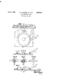
- Fig. l is a sectional view of a jig for locating the emitter and collector electrodes
- Fig. 2 is a plan view of the arrangement for attaching the base electrodes
- Fig. 3 is a sectional side view of a device after attachment of the electrodes
- Fig. 4 is a sectional side view of part of a device showing :the electrode leads in position;
- Fig. 5 shows the leads inserted into the electrodes
- FIG. 6 shows the leads and electrodes at a later stage
- Fig. 7 is a sectional 'view of a completed germanium transistor.
- a germanium transistor comprises a slice 1 of germanium of predetermined conductivity, say 1 ohm-cm. N-type, of suitable dimensions which may be one tenth of an inch square by two thousandths of an inch thick.
- the base electrode 6 surrounds one of the other electrodes,
- the emitter electrode 2 and consists of molybdenum wire about four thousandths of an inch in diameter having a lead out end 7.
- the attachment of the indium pellets 2, 3 to the slice 1 cause zones of P-type conductivity germanium to be formed respectively at 8, 9.
- the emitter and collector electrodes will have to comprise a donor impurity such as antimony or a lead-antimony alloy.
- a jig. 10 having-a central recess 11 into which the slice 1 fits snugly.
- a plate 12 having a central hole 13 large enough to locate a pellet 1 4 of indium.
- Both the jig 10 and the plate 12 or at leastthose parts thereof which come into contact with the slice 1 andthe-pel1et14 should be made of: V
- the indium pellet iscaused to melt and form a dome-shaped electrode upon the surface of the slice.
- a suitable heat cycle' for such an operation is to bringthe assembly upto temperature of between 340 C. and 380 C. (nominally 350 C.). in-i15 minutes; in say an atmosphere of hydrogen, retain there atfor 10 minutes and then cool to room tem-. perature.
- the slice is now turned over so that the dome ofrindium locates in the hole 15 in the jig. '10.
- a second pellet is inserted into the hole' 13 and the assemblyds againraised to between 340 C. and.380 C. (nominally 350 C.) in hydrogenin 15 minutes andheld thereat. for. 10 .minutes.
- the temperature is now raised in 15 minutes to between 475 C. and 590 C.v (nominally.550 C.) in hydrogen and held for. 10 minutes after which the assembly is cooled at a rate of 20 C. per minute down to at least 350 C. and then down to room. temperature.
- Prtype conductivity zones such as 8 and 9, Fig. 7.
- the indium shall enter uniformly and thus. present twovflat uniformly spaced zones 8, 9, the surfaces of: the slice 1 should be parallel and in the 1-,-l-.-1 plane of the crystal structure.
- the indium pellets are cleaned, just prior to this treatment by. dipping in concentrated nitric acid and thereafter washed and. dried.
- the probes 18, 19 serve to keep the ring in position and to pass a DC. or alternating current around the ring from one probe to the other of such value and duratio'n that the gold coating on the ring begins to flow, the gold thereby welding the ring to the slice as seen .at 20 in Fig. 3. Undue heating of the semiconductor should be avoided.
- Leads' 4, 5 are now applied totheindium electrodes either separately or together. It has been found that if a lead, ofsay platinum wire, is placed in contact with one of the indium electrodes as in Fig- 4, and a current is passed therebetween, the electrode can be made to melt andthe lead be pushed into and embedded in the indium to any desired depth, as in Fig.5, without disturbing the opposite type conductivity zone underneath. Thereafter the indium electrode material may be caused to remeltand wet the lead and tend to flow up it, as in Fig. 6, thus making goodrelectrical contact therewith,
- the completed transistor which now appears as in Fig. 7 may be washed and given an overall etch in known manner to clean it, up, the exposed parts being only semiconductor, indium and platinum or other noble metal.
- the slice 1 comprisesP-type conductivity germanium
- -a donor instead of an acceptor material is used for.
- the emitter and colleetor electrodes e.g. antimony or lead-antimony alloy in place of the indium.
- the flash plating, of antimony on the gold plated molybdenum wire, the purpose of which was to ensure that no P-type conductivity zone was formed at the base electrode, is not now required.
- theslice 1 may be prepared v remaining planar.
- germanium may be replaced by other suitable semiconductor or semiconductors.
- silicon or intermetallic compounds may be used for the slice 1 together with: appropriate donor and acceptor materials for the electrodes.
- a method of making a transistor which comprises the steps of locating in a graphite jig. a first pellet of indium on a first surface of a crystal of N-type germanium cut in the 1.1.1. plane, raising the temperature of the assembly in the jig in an atmosphereof oxygen free hydrogen at asteady rate in a time interval of approximately 15 minutes to a first elevated temperature between 340 C. and 380 C., maintaining said first elevated temperature for a period of approximately 10 minutes, cooling to room temperature, locating in the jig a second pellet of indium on a second surface of the crystal opposite said first surface, said first and second pellets being substantially opposite one another, again raisingthe temperature of the assembly in thejig in said atmos:
- a method of making a transistor which comprises the steps of locating in a graphite jig a first pellet of antimony on a first surface of a crystal of P-type germanium cut in the 1.1.1. plane, raising the temperature of the assembly in the jig in an atmosphere of oxygen free hydrogen at a steady rate in a time interval of approximately 15 minutes to a first elevated temperature between 630 C.
Landscapes
- Engineering & Computer Science (AREA)
- Physics & Mathematics (AREA)
- Condensed Matter Physics & Semiconductors (AREA)
- General Physics & Mathematics (AREA)
- Manufacturing & Machinery (AREA)
- Computer Hardware Design (AREA)
- Microelectronics & Electronic Packaging (AREA)
- Power Engineering (AREA)
- Bipolar Transistors (AREA)
- Die Bonding (AREA)
Applications Claiming Priority (4)
| Application Number | Priority Date | Filing Date | Title |
|---|---|---|---|
| GB2711156A GB801442A (en) | 1956-09-05 | 1956-09-05 | Improvements in or relating to semi-conductor devices |
| GB26120/58A GB891934A (en) | 1958-08-14 | 1958-08-14 | Improvements in or relating to semi-conductor devices |
| GB40175/58A GB907942A (en) | 1958-12-12 | 1958-12-12 | Improvements in or relating to transistors |
| GB1262761A GB909377A (en) | 1961-04-07 | 1961-04-07 | Improvements in or relating to semiconductor devices |
Publications (1)
| Publication Number | Publication Date |
|---|---|
| US2939205A true US2939205A (en) | 1960-06-07 |
Family
ID=27448152
Family Applications (2)
| Application Number | Title | Priority Date | Filing Date |
|---|---|---|---|
| US681045A Expired - Lifetime US2939205A (en) | 1956-09-05 | 1957-08-29 | Semi-conductor devices |
| US857983A Expired - Lifetime US3040219A (en) | 1956-09-05 | 1959-12-07 | Transistors |
Family Applications After (1)
| Application Number | Title | Priority Date | Filing Date |
|---|---|---|---|
| US857983A Expired - Lifetime US3040219A (en) | 1956-09-05 | 1959-12-07 | Transistors |
Country Status (6)
| Country | Link |
|---|---|
| US (2) | US2939205A (nl) |
| BE (1) | BE560551A (nl) |
| CH (2) | CH357470A (nl) |
| DE (1) | DE1158179B (nl) |
| FR (1) | FR1189146A (nl) |
| NL (1) | NL276978A (nl) |
Cited By (9)
| Publication number | Priority date | Publication date | Assignee | Title |
|---|---|---|---|---|
| US3073006A (en) * | 1958-09-16 | 1963-01-15 | Westinghouse Electric Corp | Method and apparatus for the fabrication of alloyed transistors |
| US3087450A (en) * | 1959-03-18 | 1963-04-30 | Ass Elect Ind | Manufacture of transistors |
| US3095622A (en) * | 1958-06-11 | 1963-07-02 | Clevite Corp | Apparatus for manufacture of alloyed semiconductor devices |
| US3140683A (en) * | 1960-07-06 | 1964-07-14 | Clevite Corp | Alloying fixture |
| US3150013A (en) * | 1960-02-17 | 1964-09-22 | Gen Motors Corp | Means and method for fabricating semiconductor devices |
| US3176376A (en) * | 1958-04-24 | 1965-04-06 | Motorola Inc | Method of making semiconductor device |
| US3186046A (en) * | 1959-06-10 | 1965-06-01 | Clevite Corp | Apparatus for the preparation of alloy contacts |
| US3261728A (en) * | 1961-05-25 | 1966-07-19 | Philips Corp | Method of alloying electrodes to a semiconductor body |
| US3619736A (en) * | 1970-06-22 | 1971-11-09 | Mitsumi Electric Co Ltd | Alloy junction transistor and a method of making the same |
Families Citing this family (6)
| Publication number | Priority date | Publication date | Assignee | Title |
|---|---|---|---|---|
| CH376187A (de) * | 1959-10-13 | 1964-03-31 | Transistor Ag | Verfahren zur Herstellung eines Halbleiter-Schaltelementes |
| DE1464669B1 (de) * | 1961-03-06 | 1971-02-04 | Itt Ind Gmbh Deutsche | Halbleiterdiode mit stark spannungsabhaengiger Kapazitaet |
| US3210225A (en) * | 1961-08-18 | 1965-10-05 | Texas Instruments Inc | Method of making transistor |
| US3253098A (en) * | 1963-10-24 | 1966-05-24 | Allis Chalmers Mfg Co | Mechanical actuator with permanent magnet |
| US3409482A (en) * | 1964-12-30 | 1968-11-05 | Sprague Electric Co | Method of making a transistor with a very thin diffused base and an epitaxially grown emitter |
| US3538401A (en) * | 1968-04-11 | 1970-11-03 | Westinghouse Electric Corp | Drift field thyristor |
Citations (7)
| Publication number | Priority date | Publication date | Assignee | Title |
|---|---|---|---|---|
| GB697869A (en) * | 1951-05-11 | 1953-09-30 | Post Office | Improvements in or relating to methods of mounting piezo-electric elements |
| US2671156A (en) * | 1950-10-19 | 1954-03-02 | Hazeltine Research Inc | Method of producing electrical crystal-contact devices |
| US2701326A (en) * | 1949-11-30 | 1955-02-01 | Bell Telephone Labor Inc | Semiconductor translating device |
| US2756483A (en) * | 1953-05-11 | 1956-07-31 | Sylvania Electric Prod | Junction forming crucible |
| US2758261A (en) * | 1952-06-02 | 1956-08-07 | Rca Corp | Protection of semiconductor devices |
| US2796563A (en) * | 1955-06-10 | 1957-06-18 | Bell Telephone Labor Inc | Semiconductive devices |
| US2820932A (en) * | 1956-03-07 | 1958-01-21 | Bell Telephone Labor Inc | Contact structure |
Family Cites Families (9)
| Publication number | Priority date | Publication date | Assignee | Title |
|---|---|---|---|---|
| US2811653A (en) * | 1953-05-22 | 1957-10-29 | Rca Corp | Semiconductor devices |
| DE1036393B (de) * | 1954-08-05 | 1958-08-14 | Siemens Ag | Verfahren zur Herstellung von zwei p-n-UEbergaengen in Halbleiterkoerpern, z. B. Flaechentransistoren |
| US2895058A (en) * | 1954-09-23 | 1959-07-14 | Rca Corp | Semiconductor devices and systems |
| NL204361A (nl) * | 1955-04-22 | 1900-01-01 | ||
| US2777101A (en) * | 1955-08-01 | 1957-01-08 | Cohen Jerrold | Junction transistor |
| NL121810C (nl) * | 1955-11-04 | |||
| GB800296A (en) * | 1956-11-19 | 1958-08-20 | Texas Instruments Inc | Manufacture of junction-containing silicon crystals |
| US2953488A (en) * | 1958-12-26 | 1960-09-20 | Shockley William | P-n junction having minimum transition layer capacitance |
| US2937324A (en) * | 1959-02-05 | 1960-05-17 | Westinghouse Electric Corp | Silicon carbide rectifier |
-
0
- BE BE560551D patent/BE560551A/xx unknown
- NL NL276978D patent/NL276978A/xx unknown
-
1957
- 1957-08-29 US US681045A patent/US2939205A/en not_active Expired - Lifetime
- 1957-09-03 FR FR1189146D patent/FR1189146A/fr not_active Expired
- 1957-09-05 CH CH357470D patent/CH357470A/de unknown
-
1959
- 1959-12-04 DE DEI17331A patent/DE1158179B/de active Pending
- 1959-12-07 US US857983A patent/US3040219A/en not_active Expired - Lifetime
- 1959-12-10 CH CH8166259A patent/CH377449A/de unknown
Patent Citations (7)
| Publication number | Priority date | Publication date | Assignee | Title |
|---|---|---|---|---|
| US2701326A (en) * | 1949-11-30 | 1955-02-01 | Bell Telephone Labor Inc | Semiconductor translating device |
| US2671156A (en) * | 1950-10-19 | 1954-03-02 | Hazeltine Research Inc | Method of producing electrical crystal-contact devices |
| GB697869A (en) * | 1951-05-11 | 1953-09-30 | Post Office | Improvements in or relating to methods of mounting piezo-electric elements |
| US2758261A (en) * | 1952-06-02 | 1956-08-07 | Rca Corp | Protection of semiconductor devices |
| US2756483A (en) * | 1953-05-11 | 1956-07-31 | Sylvania Electric Prod | Junction forming crucible |
| US2796563A (en) * | 1955-06-10 | 1957-06-18 | Bell Telephone Labor Inc | Semiconductive devices |
| US2820932A (en) * | 1956-03-07 | 1958-01-21 | Bell Telephone Labor Inc | Contact structure |
Cited By (9)
| Publication number | Priority date | Publication date | Assignee | Title |
|---|---|---|---|---|
| US3176376A (en) * | 1958-04-24 | 1965-04-06 | Motorola Inc | Method of making semiconductor device |
| US3095622A (en) * | 1958-06-11 | 1963-07-02 | Clevite Corp | Apparatus for manufacture of alloyed semiconductor devices |
| US3073006A (en) * | 1958-09-16 | 1963-01-15 | Westinghouse Electric Corp | Method and apparatus for the fabrication of alloyed transistors |
| US3087450A (en) * | 1959-03-18 | 1963-04-30 | Ass Elect Ind | Manufacture of transistors |
| US3186046A (en) * | 1959-06-10 | 1965-06-01 | Clevite Corp | Apparatus for the preparation of alloy contacts |
| US3150013A (en) * | 1960-02-17 | 1964-09-22 | Gen Motors Corp | Means and method for fabricating semiconductor devices |
| US3140683A (en) * | 1960-07-06 | 1964-07-14 | Clevite Corp | Alloying fixture |
| US3261728A (en) * | 1961-05-25 | 1966-07-19 | Philips Corp | Method of alloying electrodes to a semiconductor body |
| US3619736A (en) * | 1970-06-22 | 1971-11-09 | Mitsumi Electric Co Ltd | Alloy junction transistor and a method of making the same |
Also Published As
| Publication number | Publication date |
|---|---|
| US3040219A (en) | 1962-06-19 |
| CH357470A (de) | 1961-10-15 |
| CH377449A (de) | 1964-05-15 |
| NL276978A (nl) | |
| DE1158179B (de) | 1963-11-28 |
| FR1189146A (fr) | 1959-09-29 |
| BE560551A (nl) |
Similar Documents
| Publication | Publication Date | Title |
|---|---|---|
| US2939205A (en) | Semi-conductor devices | |
| US2742383A (en) | Germanium junction-type semiconductor devices | |
| US2842831A (en) | Manufacture of semiconductor devices | |
| US2796563A (en) | Semiconductive devices | |
| US2894862A (en) | Method of fabricating p-n type junction devices | |
| US3025439A (en) | Mounting for silicon semiconductor device | |
| US2784300A (en) | Method of fabricating an electrical connection | |
| GB807959A (en) | Fused junction semiconductor devices | |
| US2905873A (en) | Semiconductor power devices and method of manufacture | |
| US2825667A (en) | Methods of making surface alloyed semiconductor devices | |
| US3212160A (en) | Method of manufacturing semiconductive devices | |
| US2943006A (en) | Diffused transistors and processes for making the same | |
| US3022452A (en) | Diode | |
| US2820135A (en) | Method for producing electrical contact to semiconductor devices | |
| US2877396A (en) | Semi-conductor devices | |
| US3297855A (en) | Method of bonding | |
| US2887415A (en) | Method of making alloyed junction in a silicon wafer | |
| US2817798A (en) | Semiconductors | |
| US2918719A (en) | Semi-conductor devices and methods of making them | |
| US2996800A (en) | Method of making ohmic connections to silicon semiconductors | |
| US3099776A (en) | Indium antimonide transistor | |
| US3249829A (en) | Encapsulated diode assembly | |
| US3089067A (en) | Semiconductor device | |
| US2874083A (en) | Transistor construction | |
| US2796368A (en) | Method of making semi-conductor devices |