US20130169148A1 - Highly efficient phosphorescent materials - Google Patents
Highly efficient phosphorescent materials Download PDFInfo
- Publication number
- US20130169148A1 US20130169148A1 US13/345,285 US201213345285A US2013169148A1 US 20130169148 A1 US20130169148 A1 US 20130169148A1 US 201213345285 A US201213345285 A US 201213345285A US 2013169148 A1 US2013169148 A1 US 2013169148A1
- Authority
- US
- United States
- Prior art keywords
- compound
- group
- alkyl
- combinations
- formula
- Prior art date
- Legal status (The legal status is an assumption and is not a legal conclusion. Google has not performed a legal analysis and makes no representation as to the accuracy of the status listed.)
- Granted
Links
- 239000000463 material Substances 0.000 title description 64
- 125000000217 alkyl group Chemical group 0.000 claims abstract description 40
- 238000006467 substitution reaction Methods 0.000 claims abstract description 15
- 150000001875 compounds Chemical class 0.000 claims description 79
- -1 amino, silyl Chemical group 0.000 claims description 34
- 229910052751 metal Inorganic materials 0.000 claims description 33
- 239000002184 metal Substances 0.000 claims description 33
- 125000003118 aryl group Chemical group 0.000 claims description 27
- 125000000753 cycloalkyl group Chemical group 0.000 claims description 20
- 125000001072 heteroaryl group Chemical group 0.000 claims description 20
- YZCKVEUIGOORGS-OUBTZVSYSA-N Deuterium Chemical compound [2H] YZCKVEUIGOORGS-OUBTZVSYSA-N 0.000 claims description 16
- 229910052805 deuterium Inorganic materials 0.000 claims description 16
- 125000004404 heteroalkyl group Chemical group 0.000 claims description 16
- 229910052739 hydrogen Inorganic materials 0.000 claims description 16
- 239000001257 hydrogen Substances 0.000 claims description 16
- 125000004432 carbon atom Chemical group C* 0.000 claims description 13
- 150000002431 hydrogen Chemical class 0.000 claims description 13
- 239000012044 organic layer Substances 0.000 claims description 13
- 125000003342 alkenyl group Chemical group 0.000 claims description 12
- 125000000959 isobutyl group Chemical group [H]C([H])([H])C([H])(C([H])([H])[H])C([H])([H])* 0.000 claims description 12
- 125000000472 sulfonyl group Chemical group *S(*)(=O)=O 0.000 claims description 12
- 150000002148 esters Chemical class 0.000 claims description 11
- 125000002252 acyl group Chemical group 0.000 claims description 10
- 125000003545 alkoxy group Chemical group 0.000 claims description 10
- 125000000304 alkynyl group Chemical group 0.000 claims description 10
- 125000003710 aryl alkyl group Chemical group 0.000 claims description 10
- 125000004104 aryloxy group Chemical group 0.000 claims description 10
- 125000002915 carbonyl group Chemical group [*:2]C([*:1])=O 0.000 claims description 10
- 150000001735 carboxylic acids Chemical class 0.000 claims description 10
- 125000000392 cycloalkenyl group Chemical group 0.000 claims description 10
- 150000004820 halides Chemical class 0.000 claims description 10
- 150000002527 isonitriles Chemical class 0.000 claims description 10
- 150000002825 nitriles Chemical class 0.000 claims description 10
- 125000003396 thiol group Chemical group [H]S* 0.000 claims description 10
- FVZVCSNXTFCBQU-UHFFFAOYSA-N phosphanyl Chemical group [PH2] FVZVCSNXTFCBQU-UHFFFAOYSA-N 0.000 claims description 9
- 125000000475 sulfinyl group Chemical group [*:2]S([*:1])=O 0.000 claims description 7
- UHBIKXOBLZWFKM-UHFFFAOYSA-N 8-hydroxy-2-quinolinecarboxylic acid Chemical compound C1=CC=C(O)C2=NC(C(=O)O)=CC=C21 UHBIKXOBLZWFKM-UHFFFAOYSA-N 0.000 claims description 6
- 125000000113 cyclohexyl group Chemical group [H]C1([H])C([H])([H])C([H])([H])C([H])(*)C([H])([H])C1([H])[H] 0.000 claims description 6
- 125000001449 isopropyl group Chemical group [H]C([H])([H])C([H])(*)C([H])([H])[H] 0.000 claims description 6
- 125000004435 hydrogen atom Chemical group [H]* 0.000 claims description 4
- 125000001511 cyclopentyl group Chemical group [H]C1([H])C([H])([H])C([H])([H])C([H])(*)C1([H])[H] 0.000 claims description 3
- 125000002496 methyl group Chemical group [H]C([H])([H])* 0.000 claims description 3
- 125000001997 phenyl group Chemical group [H]C1=C([H])C([H])=C(*)C([H])=C1[H] 0.000 claims description 3
- 239000003446 ligand Substances 0.000 abstract description 32
- FSEXLNMNADBYJU-UHFFFAOYSA-N 2-phenylquinoline Chemical class C1=CC=CC=C1C1=CC=C(C=CC=C2)C2=N1 FSEXLNMNADBYJU-UHFFFAOYSA-N 0.000 abstract description 9
- 150000002503 iridium Chemical class 0.000 abstract description 8
- 125000001424 substituent group Chemical group 0.000 abstract description 7
- YRKCREAYFQTBPV-UHFFFAOYSA-N acetylacetone Chemical compound CC(=O)CC(C)=O YRKCREAYFQTBPV-UHFFFAOYSA-N 0.000 abstract description 4
- 239000010410 layer Substances 0.000 description 64
- YMWUJEATGCHHMB-UHFFFAOYSA-N Dichloromethane Chemical compound ClCCl YMWUJEATGCHHMB-UHFFFAOYSA-N 0.000 description 26
- 0 *C.CC.[1*]C1=CC2=C(C=C1)C=CC1=N2[Ir]2(OC([2*])=C([3*])C([4*])=O2)C2=CC=CC=C21 Chemical compound *C.CC.[1*]C1=CC2=C(C=C1)C=CC1=N2[Ir]2(OC([2*])=C([3*])C([4*])=O2)C2=CC=CC=C21 0.000 description 24
- IJGRMHOSHXDMSA-UHFFFAOYSA-N Atomic nitrogen Chemical compound N#N IJGRMHOSHXDMSA-UHFFFAOYSA-N 0.000 description 17
- 229910052757 nitrogen Inorganic materials 0.000 description 15
- 239000000047 product Substances 0.000 description 14
- 239000002019 doping agent Substances 0.000 description 13
- RAXXELZNTBOGNW-UHFFFAOYSA-N imidazole Natural products C1=CNC=N1 RAXXELZNTBOGNW-UHFFFAOYSA-N 0.000 description 12
- 150000003384 small molecules Chemical class 0.000 description 12
- 239000000243 solution Substances 0.000 description 11
- XEKOWRVHYACXOJ-UHFFFAOYSA-N Ethyl acetate Chemical compound CCOC(C)=O XEKOWRVHYACXOJ-UHFFFAOYSA-N 0.000 description 10
- KFZMGEQAYNKOFK-UHFFFAOYSA-N Isopropanol Chemical compound CC(C)O KFZMGEQAYNKOFK-UHFFFAOYSA-N 0.000 description 10
- 230000000903 blocking effect Effects 0.000 description 10
- ZMXDDKWLCZADIW-UHFFFAOYSA-N N,N-Dimethylformamide Chemical compound CN(C)C=O ZMXDDKWLCZADIW-UHFFFAOYSA-N 0.000 description 9
- VYPSYNLAJGMNEJ-UHFFFAOYSA-N Silicium dioxide Chemical compound O=[Si]=O VYPSYNLAJGMNEJ-UHFFFAOYSA-N 0.000 description 9
- 230000000052 comparative effect Effects 0.000 description 9
- 125000002524 organometallic group Chemical group 0.000 description 9
- 229920000642 polymer Polymers 0.000 description 9
- 239000011541 reaction mixture Substances 0.000 description 9
- 238000004770 highest occupied molecular orbital Methods 0.000 description 8
- 239000007924 injection Substances 0.000 description 8
- 238000002347 injection Methods 0.000 description 8
- 238000004768 lowest unoccupied molecular orbital Methods 0.000 description 8
- 239000000203 mixture Substances 0.000 description 8
- 230000032258 transport Effects 0.000 description 8
- 229940125904 compound 1 Drugs 0.000 description 7
- 238000000151 deposition Methods 0.000 description 7
- IYYZUPMFVPLQIF-UHFFFAOYSA-N dibenzothiophene Chemical compound C1=CC=C2C3=CC=CC=C3SC2=C1 IYYZUPMFVPLQIF-UHFFFAOYSA-N 0.000 description 7
- 238000000034 method Methods 0.000 description 7
- 239000000758 substrate Substances 0.000 description 7
- TVIVIEFSHFOWTE-UHFFFAOYSA-K tri(quinolin-8-yloxy)alumane Chemical compound [Al+3].C1=CN=C2C([O-])=CC=CC2=C1.C1=CN=C2C([O-])=CC=CC2=C1.C1=CN=C2C([O-])=CC=CC2=C1 TVIVIEFSHFOWTE-UHFFFAOYSA-K 0.000 description 7
- XLYOFNOQVPJJNP-UHFFFAOYSA-N water Chemical compound O XLYOFNOQVPJJNP-UHFFFAOYSA-N 0.000 description 7
- FCEHBMOGCRZNNI-UHFFFAOYSA-N 1-benzothiophene Chemical compound C1=CC=C2SC=CC2=C1 FCEHBMOGCRZNNI-UHFFFAOYSA-N 0.000 description 6
- UJOBWOGCFQCDNV-UHFFFAOYSA-N 9H-carbazole Chemical compound C1=CC=C2C3=CC=CC=C3NC2=C1 UJOBWOGCFQCDNV-UHFFFAOYSA-N 0.000 description 6
- UHOVQNZJYSORNB-UHFFFAOYSA-N Benzene Chemical compound C1=CC=CC=C1 UHOVQNZJYSORNB-UHFFFAOYSA-N 0.000 description 6
- YXFVVABEGXRONW-UHFFFAOYSA-N Toluene Chemical compound CC1=CC=CC=C1 YXFVVABEGXRONW-UHFFFAOYSA-N 0.000 description 6
- 125000000623 heterocyclic group Chemical group 0.000 description 6
- VLKZOEOYAKHREP-UHFFFAOYSA-N n-Hexane Chemical class CCCCCC VLKZOEOYAKHREP-UHFFFAOYSA-N 0.000 description 6
- 239000011368 organic material Substances 0.000 description 6
- 229910052760 oxygen Inorganic materials 0.000 description 6
- XSCHRSMBECNVNS-UHFFFAOYSA-N quinoxaline Chemical compound N1=CC=NC2=CC=CC=C21 XSCHRSMBECNVNS-UHFFFAOYSA-N 0.000 description 6
- DHDHJYNTEFLIHY-UHFFFAOYSA-N 4,7-diphenyl-1,10-phenanthroline Chemical group C1=CC=CC=C1C1=CC=NC2=C1C=CC1=C(C=3C=CC=CC=3)C=CN=C21 DHDHJYNTEFLIHY-UHFFFAOYSA-N 0.000 description 5
- 229910052799 carbon Inorganic materials 0.000 description 5
- 239000000412 dendrimer Substances 0.000 description 5
- 229920000736 dendritic polymer Polymers 0.000 description 5
- TXCDCPKCNAJMEE-UHFFFAOYSA-N dibenzofuran Chemical compound C1=CC=C2C3=CC=CC=C3OC2=C1 TXCDCPKCNAJMEE-UHFFFAOYSA-N 0.000 description 5
- 230000005525 hole transport Effects 0.000 description 5
- IBHBKWKFFTZAHE-UHFFFAOYSA-N n-[4-[4-(n-naphthalen-1-ylanilino)phenyl]phenyl]-n-phenylnaphthalen-1-amine Chemical group C1=CC=CC=C1N(C=1C2=CC=CC=C2C=CC=1)C1=CC=C(C=2C=CC(=CC=2)N(C=2C=CC=CC=2)C=2C3=CC=CC=C3C=CC=2)C=C1 IBHBKWKFFTZAHE-UHFFFAOYSA-N 0.000 description 5
- 230000005693 optoelectronics Effects 0.000 description 5
- 150000002894 organic compounds Chemical class 0.000 description 5
- WCPAKWJPBJAGKN-UHFFFAOYSA-N oxadiazole Chemical compound C1=CON=N1 WCPAKWJPBJAGKN-UHFFFAOYSA-N 0.000 description 5
- 229910052698 phosphorus Inorganic materials 0.000 description 5
- 229910052717 sulfur Inorganic materials 0.000 description 5
- 150000003852 triazoles Chemical class 0.000 description 5
- HYZJCKYKOHLVJF-UHFFFAOYSA-N 1H-benzimidazole Chemical compound C1=CC=C2NC=NC2=C1 HYZJCKYKOHLVJF-UHFFFAOYSA-N 0.000 description 4
- OKTJSMMVPCPJKN-UHFFFAOYSA-N Carbon Chemical group [C] OKTJSMMVPCPJKN-UHFFFAOYSA-N 0.000 description 4
- YLQBMQCUIZJEEH-UHFFFAOYSA-N Furan Chemical compound C=1C=COC=1 YLQBMQCUIZJEEH-UHFFFAOYSA-N 0.000 description 4
- SIKJAQJRHWYJAI-UHFFFAOYSA-N Indole Chemical compound C1=CC=C2NC=CC2=C1 SIKJAQJRHWYJAI-UHFFFAOYSA-N 0.000 description 4
- UFWIBTONFRDIAS-UHFFFAOYSA-N Naphthalene Chemical compound C1=CC=CC2=CC=CC=C21 UFWIBTONFRDIAS-UHFFFAOYSA-N 0.000 description 4
- PCNDJXKNXGMECE-UHFFFAOYSA-N Phenazine Natural products C1=CC=CC2=NC3=CC=CC=C3N=C21 PCNDJXKNXGMECE-UHFFFAOYSA-N 0.000 description 4
- KYQCOXFCLRTKLS-UHFFFAOYSA-N Pyrazine Chemical compound C1=CN=CC=N1 KYQCOXFCLRTKLS-UHFFFAOYSA-N 0.000 description 4
- JUJWROOIHBZHMG-UHFFFAOYSA-N Pyridine Chemical compound C1=CC=NC=C1 JUJWROOIHBZHMG-UHFFFAOYSA-N 0.000 description 4
- SMWDFEZZVXVKRB-UHFFFAOYSA-N Quinoline Chemical compound N1=CC=CC2=CC=CC=C21 SMWDFEZZVXVKRB-UHFFFAOYSA-N 0.000 description 4
- YTPLMLYBLZKORZ-UHFFFAOYSA-N Thiophene Chemical compound C=1C=CSC=1 YTPLMLYBLZKORZ-UHFFFAOYSA-N 0.000 description 4
- DZBUGLKDJFMEHC-UHFFFAOYSA-N acridine Chemical compound C1=CC=CC2=CC3=CC=CC=C3N=C21 DZBUGLKDJFMEHC-UHFFFAOYSA-N 0.000 description 4
- MWPLVEDNUUSJAV-UHFFFAOYSA-N anthracene Chemical compound C1=CC=CC2=CC3=CC=CC=C3C=C21 MWPLVEDNUUSJAV-UHFFFAOYSA-N 0.000 description 4
- 125000006615 aromatic heterocyclic group Chemical group 0.000 description 4
- CUFNKYGDVFVPHO-UHFFFAOYSA-N azulene Chemical compound C1=CC=CC2=CC=CC2=C1 CUFNKYGDVFVPHO-UHFFFAOYSA-N 0.000 description 4
- IOJUPLGTWVMSFF-UHFFFAOYSA-N benzothiazole Chemical compound C1=CC=C2SC=NC2=C1 IOJUPLGTWVMSFF-UHFFFAOYSA-N 0.000 description 4
- 238000006243 chemical reaction Methods 0.000 description 4
- WDECIBYCCFPHNR-UHFFFAOYSA-N chrysene Chemical compound C1=CC=CC2=CC=C3C4=CC=CC=C4C=CC3=C21 WDECIBYCCFPHNR-UHFFFAOYSA-N 0.000 description 4
- 150000004696 coordination complex Chemical class 0.000 description 4
- 125000004122 cyclic group Chemical group 0.000 description 4
- ZUOUZKKEUPVFJK-UHFFFAOYSA-N diphenyl Chemical compound C1=CC=CC=C1C1=CC=CC=C1 ZUOUZKKEUPVFJK-UHFFFAOYSA-N 0.000 description 4
- 239000000706 filtrate Substances 0.000 description 4
- VVVPGLRKXQSQSZ-UHFFFAOYSA-N indolo[3,2-c]carbazole Chemical class C1=CC=CC2=NC3=C4C5=CC=CC=C5N=C4C=CC3=C21 VVVPGLRKXQSQSZ-UHFFFAOYSA-N 0.000 description 4
- 229910052741 iridium Inorganic materials 0.000 description 4
- AWJUIBRHMBBTKR-UHFFFAOYSA-N isoquinoline Chemical compound C1=NC=CC2=CC=CC=C21 AWJUIBRHMBBTKR-UHFFFAOYSA-N 0.000 description 4
- YNPNZTXNASCQKK-UHFFFAOYSA-N phenanthrene Chemical compound C1=CC=C2C3=CC=CC=C3C=CC2=C1 YNPNZTXNASCQKK-UHFFFAOYSA-N 0.000 description 4
- BASFCYQUMIYNBI-UHFFFAOYSA-N platinum Substances [Pt] BASFCYQUMIYNBI-UHFFFAOYSA-N 0.000 description 4
- LVTJOONKWUXEFR-FZRMHRINSA-N protoneodioscin Natural products O(C[C@@H](CC[C@]1(O)[C@H](C)[C@@H]2[C@]3(C)[C@H]([C@H]4[C@@H]([C@]5(C)C(=CC4)C[C@@H](O[C@@H]4[C@H](O[C@H]6[C@@H](O)[C@@H](O)[C@@H](O)[C@H](C)O6)[C@@H](O)[C@H](O[C@H]6[C@@H](O)[C@@H](O)[C@@H](O)[C@H](C)O6)[C@H](CO)O4)CC5)CC3)C[C@@H]2O1)C)[C@H]1[C@H](O)[C@H](O)[C@H](O)[C@@H](CO)O1 LVTJOONKWUXEFR-FZRMHRINSA-N 0.000 description 4
- BBEAQIROQSPTKN-UHFFFAOYSA-N pyrene Chemical compound C1=CC=C2C=CC3=CC=CC4=CC=C1C2=C43 BBEAQIROQSPTKN-UHFFFAOYSA-N 0.000 description 4
- 229910052710 silicon Inorganic materials 0.000 description 4
- 125000005259 triarylamine group Chemical group 0.000 description 4
- 125000005580 triphenylene group Chemical group 0.000 description 4
- ZNQVEEAIQZEUHB-UHFFFAOYSA-N 2-ethoxyethanol Chemical compound CCOCCO ZNQVEEAIQZEUHB-UHFFFAOYSA-N 0.000 description 3
- 229940093475 2-ethoxyethanol Drugs 0.000 description 3
- OZDOJLFRRGLSLU-UHFFFAOYSA-J C1=CC(C2=CC3=C(C=C2)C=C(C2=CC4=C(C=CC=C4)C=C2)C=C3)=CC(C2=C3C=CC=CC3=C3/C=C\C=C/C3=C2)=C1.C1=CC=C2C(=C1)OCN1=C2SC2=C1C=CC=C2.CC1=N2/C3=C(C=CC=C3O[Al]2OC2=CC3=C(C=C2)C=C(C2=CC=CC=C2)C=C3)/C=C\1.CC1=N2C3=C(C=CC=C3O[Al]2OC2=CC=C(C3=CC=CC=C3)C=C2)C=C1 Chemical compound C1=CC(C2=CC3=C(C=C2)C=C(C2=CC4=C(C=CC=C4)C=C2)C=C3)=CC(C2=C3C=CC=CC3=C3/C=C\C=C/C3=C2)=C1.C1=CC=C2C(=C1)OCN1=C2SC2=C1C=CC=C2.CC1=N2/C3=C(C=CC=C3O[Al]2OC2=CC3=C(C=C2)C=C(C2=CC=CC=C2)C=C3)/C=C\1.CC1=N2C3=C(C=CC=C3O[Al]2OC2=CC=C(C3=CC=CC=C3)C=C2)C=C1 OZDOJLFRRGLSLU-UHFFFAOYSA-J 0.000 description 3
- ATUOYWHBWRKTHZ-UHFFFAOYSA-N CCC Chemical compound CCC ATUOYWHBWRKTHZ-UHFFFAOYSA-N 0.000 description 3
- OKKJLVBELUTLKV-UHFFFAOYSA-N Methanol Chemical compound OC OKKJLVBELUTLKV-UHFFFAOYSA-N 0.000 description 3
- XUIMIQQOPSSXEZ-UHFFFAOYSA-N Silicon Chemical group [Si] XUIMIQQOPSSXEZ-UHFFFAOYSA-N 0.000 description 3
- HEMHJVSKTPXQMS-UHFFFAOYSA-M Sodium hydroxide Chemical compound [OH-].[Na+] HEMHJVSKTPXQMS-UHFFFAOYSA-M 0.000 description 3
- WYURNTSHIVDZCO-UHFFFAOYSA-N Tetrahydrofuran Chemical compound C1CCOC1 WYURNTSHIVDZCO-UHFFFAOYSA-N 0.000 description 3
- 150000004982 aromatic amines Chemical class 0.000 description 3
- 239000003086 colorant Substances 0.000 description 3
- 229940125782 compound 2 Drugs 0.000 description 3
- 239000012043 crude product Substances 0.000 description 3
- 230000002950 deficient Effects 0.000 description 3
- 238000010586 diagram Methods 0.000 description 3
- RMBPEFMHABBEKP-UHFFFAOYSA-N fluorene Chemical compound C1=CC=C2C3=C[CH]C=CC3=CC2=C1 RMBPEFMHABBEKP-UHFFFAOYSA-N 0.000 description 3
- 229960005544 indolocarbazole Drugs 0.000 description 3
- MILUBEOXRNEUHS-UHFFFAOYSA-N iridium(3+) Chemical compound [Ir+3] MILUBEOXRNEUHS-UHFFFAOYSA-N 0.000 description 3
- 230000007246 mechanism Effects 0.000 description 3
- HZVOZRGWRWCICA-UHFFFAOYSA-N methanediyl Chemical compound [CH2] HZVOZRGWRWCICA-UHFFFAOYSA-N 0.000 description 3
- NIHNNTQXNPWCJQ-UHFFFAOYSA-N o-biphenylenemethane Natural products C1=CC=C2CC3=CC=CC=C3C2=C1 NIHNNTQXNPWCJQ-UHFFFAOYSA-N 0.000 description 3
- 239000002002 slurry Substances 0.000 description 3
- 239000002904 solvent Substances 0.000 description 3
- VNFWTIYUKDMAOP-UHFFFAOYSA-N sphos Chemical compound COC1=CC=CC(OC)=C1C1=CC=CC=C1P(C1CCCCC1)C1CCCCC1 VNFWTIYUKDMAOP-UHFFFAOYSA-N 0.000 description 3
- 238000002207 thermal evaporation Methods 0.000 description 3
- 239000011701 zinc Substances 0.000 description 3
- JYEUMXHLPRZUAT-UHFFFAOYSA-N 1,2,3-triazine Chemical compound C1=CN=NN=C1 JYEUMXHLPRZUAT-UHFFFAOYSA-N 0.000 description 2
- KTZQTRPPVKQPFO-UHFFFAOYSA-N 1,2-benzoxazole Chemical compound C1=CC=C2C=NOC2=C1 KTZQTRPPVKQPFO-UHFFFAOYSA-N 0.000 description 2
- YJTKZCDBKVTVBY-UHFFFAOYSA-N 1,3-Diphenylbenzene Chemical group C1=CC=CC=C1C1=CC=CC(C=2C=CC=CC=2)=C1 YJTKZCDBKVTVBY-UHFFFAOYSA-N 0.000 description 2
- BCMCBBGGLRIHSE-UHFFFAOYSA-N 1,3-benzoxazole Chemical compound C1=CC=C2OC=NC2=C1 BCMCBBGGLRIHSE-UHFFFAOYSA-N 0.000 description 2
- FLBAYUMRQUHISI-UHFFFAOYSA-N 1,8-naphthyridine Chemical compound N1=CC=CC2=CC=CN=C21 FLBAYUMRQUHISI-UHFFFAOYSA-N 0.000 description 2
- IANQTJSKSUMEQM-UHFFFAOYSA-N 1-benzofuran Chemical compound C1=CC=C2OC=CC2=C1 IANQTJSKSUMEQM-UHFFFAOYSA-N 0.000 description 2
- BNRDGHFESOHOBF-UHFFFAOYSA-N 1-benzoselenophene Chemical compound C1=CC=C2[se]C=CC2=C1 BNRDGHFESOHOBF-UHFFFAOYSA-N 0.000 description 2
- WJFKNYWRSNBZNX-UHFFFAOYSA-N 10H-phenothiazine Chemical compound C1=CC=C2NC3=CC=CC=C3SC2=C1 WJFKNYWRSNBZNX-UHFFFAOYSA-N 0.000 description 2
- TZMSYXZUNZXBOL-UHFFFAOYSA-N 10H-phenoxazine Chemical compound C1=CC=C2NC3=CC=CC=C3OC2=C1 TZMSYXZUNZXBOL-UHFFFAOYSA-N 0.000 description 2
- BAXOFTOLAUCFNW-UHFFFAOYSA-N 1H-indazole Chemical compound C1=CC=C2C=NNC2=C1 BAXOFTOLAUCFNW-UHFFFAOYSA-N 0.000 description 2
- VEPOHXYIFQMVHW-XOZOLZJESA-N 2,3-dihydroxybutanedioic acid (2S,3S)-3,4-dimethyl-2-phenylmorpholine Chemical compound OC(C(O)C(O)=O)C(O)=O.C[C@H]1[C@@H](OCCN1C)c1ccccc1 VEPOHXYIFQMVHW-XOZOLZJESA-N 0.000 description 2
- GJMUCDMIIVSROW-UHFFFAOYSA-N 2,8-dimethylnonane-4,6-dione Chemical compound CC(C)CC(=O)CC(=O)CC(C)C GJMUCDMIIVSROW-UHFFFAOYSA-N 0.000 description 2
- OLGGLCIDAMICTA-UHFFFAOYSA-N 2-pyridin-2-yl-1h-indole Chemical compound N1C2=CC=CC=C2C=C1C1=CC=CC=N1 OLGGLCIDAMICTA-UHFFFAOYSA-N 0.000 description 2
- QMEQBOSUJUOXMX-UHFFFAOYSA-N 2h-oxadiazine Chemical compound N1OC=CC=N1 QMEQBOSUJUOXMX-UHFFFAOYSA-N 0.000 description 2
- BCHZICNRHXRCHY-UHFFFAOYSA-N 2h-oxazine Chemical compound N1OC=CC=C1 BCHZICNRHXRCHY-UHFFFAOYSA-N 0.000 description 2
- BWCDLEQTELFBAW-UHFFFAOYSA-N 3h-dioxazole Chemical compound N1OOC=C1 BWCDLEQTELFBAW-UHFFFAOYSA-N 0.000 description 2
- GJCOSYZMQJWQCA-UHFFFAOYSA-N 9H-xanthene Chemical compound C1=CC=C2CC3=CC=CC=C3OC2=C1 GJCOSYZMQJWQCA-UHFFFAOYSA-N 0.000 description 2
- ZOXJGFHDIHLPTG-UHFFFAOYSA-N Boron Chemical group [B] ZOXJGFHDIHLPTG-UHFFFAOYSA-N 0.000 description 2
- KFKHNBPNJMWUEG-UHFFFAOYSA-N C1=CC(C2=CC=CC(C3=CC4=C(C=C3)C3=C(C=CC=C3)C3=C4C=CC=C3)=C2)=CC(C2=CC3=C(C=C2)C2=C(C=CC=C2)C2=C3C=CC=C2)=C1 Chemical compound C1=CC(C2=CC=CC(C3=CC4=C(C=C3)C3=C(C=CC=C3)C3=C4C=CC=C3)=C2)=CC(C2=CC3=C(C=C2)C2=C(C=CC=C2)C2=C3C=CC=C2)=C1 KFKHNBPNJMWUEG-UHFFFAOYSA-N 0.000 description 2
- NSXJEEMTGWMJPY-UHFFFAOYSA-N C1=CC(N2C3=C(C=CC=C3)C3=C2C=CC=C3)=CC(C2=CC=CC(N3C4=C(C=CC=C4)C4=C3C=CC=C4)=C2)=C1 Chemical compound C1=CC(N2C3=C(C=CC=C3)C3=C2C=CC=C3)=CC(C2=CC=CC(N3C4=C(C=CC=C4)C4=C3C=CC=C4)=C2)=C1 NSXJEEMTGWMJPY-UHFFFAOYSA-N 0.000 description 2
- MZYDBGLUVPLRKR-UHFFFAOYSA-N C1=CC(N2C3=C(C=CC=C3)C3=C2C=CC=C3)=CC(N2C3=C(C=CC=C3)C3=C2C=CC=C3)=C1 Chemical compound C1=CC(N2C3=C(C=CC=C3)C3=C2C=CC=C3)=CC(N2C3=C(C=CC=C3)C3=C2C=CC=C3)=C1 MZYDBGLUVPLRKR-UHFFFAOYSA-N 0.000 description 2
- SDEFDICGRVDKPH-UHFFFAOYSA-M C1=CC2=C3C(=C1)O[AlH]/N3=C/C=C\2 Chemical compound C1=CC2=C3C(=C1)O[AlH]/N3=C/C=C\2 SDEFDICGRVDKPH-UHFFFAOYSA-M 0.000 description 2
- WLLRHFOXFKWDMQ-UHFFFAOYSA-N C1=CC=C(N(C2=CC=CC=C2)C2=CC=C(C3=CC=C(N(C4=CC=CC=C4)C4=CC=C(C5=CC=C(N(C6=CC=CC=C6)C6=CC=C(C7=CC=C(N(C8=CC=CC=C8)C8=CC=CC=C8)C=C7)C=C6)C=C5)C=C4)C=C3)C=C2)C=C1 Chemical compound C1=CC=C(N(C2=CC=CC=C2)C2=CC=C(C3=CC=C(N(C4=CC=CC=C4)C4=CC=C(C5=CC=C(N(C6=CC=CC=C6)C6=CC=C(C7=CC=C(N(C8=CC=CC=C8)C8=CC=CC=C8)C=C7)C=C6)C=C5)C=C4)C=C3)C=C2)C=C1 WLLRHFOXFKWDMQ-UHFFFAOYSA-N 0.000 description 2
- GEQBRULPNIVQPP-UHFFFAOYSA-N C1=CC=C(N2C(C3=CC(/C4=N/C5=C(C=CC=C5)N4C4=CC=CC=C4)=CC(/C4=N/C5=C(C=CC=C5)N4C4=CC=CC=C4)=C3)=NC3=C2C=CC=C3)C=C1 Chemical compound C1=CC=C(N2C(C3=CC(/C4=N/C5=C(C=CC=C5)N4C4=CC=CC=C4)=CC(/C4=N/C5=C(C=CC=C5)N4C4=CC=CC=C4)=C3)=NC3=C2C=CC=C3)C=C1 GEQBRULPNIVQPP-UHFFFAOYSA-N 0.000 description 2
- XZCJVWCMJYNSQO-UHFFFAOYSA-N CC(C)(C)C1=CC=C(C2=NN=C(C3=CC=C(C4=CC=CC=C4)C=C3)O2)C=C1 Chemical compound CC(C)(C)C1=CC=C(C2=NN=C(C3=CC=C(C4=CC=CC=C4)C=C3)O2)C=C1 XZCJVWCMJYNSQO-UHFFFAOYSA-N 0.000 description 2
- FIRNXGIHIBWXDV-UHFFFAOYSA-N CC(C)(C1=CC=C(N2C3=C(C=CC=C3)C3=C2C=CC=N3)C=C1)C1=CC=C(C(C)(C)C2=CC=C(N3C4=C(C=CC=C4)C4=C3/C=C\C=N/4)C=C2)C=C1 Chemical compound CC(C)(C1=CC=C(N2C3=C(C=CC=C3)C3=C2C=CC=N3)C=C1)C1=CC=C(C(C)(C)C2=CC=C(N3C4=C(C=CC=C4)C4=C3/C=C\C=N/4)C=C2)C=C1 FIRNXGIHIBWXDV-UHFFFAOYSA-N 0.000 description 2
- JTCOZRMZCXMDFE-AWASDAIOSA-J CC1=CC(C)=C(C2=CC(C)=O[Ir]3(O2)C2=C(C)C=C(C)C=C2C2=N3C3=C(C=CC(CC(C)C)=C3)C=C2)C(C)=C1.CC1=CC(C)=C2C(=C1)C1=N(C3=C(C=CC(CC(C)C)=C3)C=C1)[Ir]21OC(C(C)C)=C2CCCCC2=O1.CC1=CC(C)=C2C(=C1)C1=N(C3=C(C=CC(CC(C)C)=C3)C=C1)[Ir]21OC(C2=CC=CC=C2)=CC(C)=O1.CC1=CC(C)=C2C(=C1)C1=N(C3=C(C=CC(CC(C)C)=C3)C=C1)[Ir]21OC(CC(C)C)=CC(C)=O1 Chemical compound CC1=CC(C)=C(C2=CC(C)=O[Ir]3(O2)C2=C(C)C=C(C)C=C2C2=N3C3=C(C=CC(CC(C)C)=C3)C=C2)C(C)=C1.CC1=CC(C)=C2C(=C1)C1=N(C3=C(C=CC(CC(C)C)=C3)C=C1)[Ir]21OC(C(C)C)=C2CCCCC2=O1.CC1=CC(C)=C2C(=C1)C1=N(C3=C(C=CC(CC(C)C)=C3)C=C1)[Ir]21OC(C2=CC=CC=C2)=CC(C)=O1.CC1=CC(C)=C2C(=C1)C1=N(C3=C(C=CC(CC(C)C)=C3)C=C1)[Ir]21OC(CC(C)C)=CC(C)=O1 JTCOZRMZCXMDFE-AWASDAIOSA-J 0.000 description 2
- YIPQMYAWYQFSED-TXXOENJCSA-J CC1=CC(C)=C2C(=C1)C1=N(C3=C(C=CC(C4CCCC4)=C3)C=C1)[Ir]21OC(C(C)C)=CC(C(C)C)=O1.CC1=CC(C)=C2C(=C1)C1=N(C3=C(C=CC(C4CCCC4)=C3)C=C1)[Ir]21OC(CC(C)C)=CC(CC(C)C)=O1.CC1=CC(C)=C2C(=C1)C1=N(C3=C(C=CC(C4CCCCC4)=C3)C=C1)[Ir]21OC(C2CCCCC2)=CC(C2CCCCC2)=O1.CC1=CC(C)=C2C(=C1)C1=N(C3=C(C=CC(C4CCCCC4)=C3)C=C1)[Ir]21OC(CC(C)C)=CC(CC(C)C)=O1 Chemical compound CC1=CC(C)=C2C(=C1)C1=N(C3=C(C=CC(C4CCCC4)=C3)C=C1)[Ir]21OC(C(C)C)=CC(C(C)C)=O1.CC1=CC(C)=C2C(=C1)C1=N(C3=C(C=CC(C4CCCC4)=C3)C=C1)[Ir]21OC(CC(C)C)=CC(CC(C)C)=O1.CC1=CC(C)=C2C(=C1)C1=N(C3=C(C=CC(C4CCCCC4)=C3)C=C1)[Ir]21OC(C2CCCCC2)=CC(C2CCCCC2)=O1.CC1=CC(C)=C2C(=C1)C1=N(C3=C(C=CC(C4CCCCC4)=C3)C=C1)[Ir]21OC(CC(C)C)=CC(CC(C)C)=O1 YIPQMYAWYQFSED-TXXOENJCSA-J 0.000 description 2
- KQWNVFBKERARNY-GGDQAKJYSA-J CC1=CC(C)=C2C(=C1)C1=N(C3=C(C=CC(C4CCCC4)=C3)C=C1)[Ir]21OC(C)=C(C2=CC=CC=C2)C(C)=O1.CC1=CC(C)=C2C(=C1)C1=N(C3=C(C=CC(C4CCCCC4)=C3)C=C1)[Ir]21OC(C)=C(C2=CC=CC=C2)C(C)=O1.CC1=CC(C)=C2C(=C1)C1=N(C3=C(C=CC(CC(C)(C)C)=C3)C=C1)[Ir]21OC(C)=C(C2=CC=CC=C2)C(C)=O1.CC1=CC(C)=C2C(=C1)C1=N(C3=C(C=CC(CC(C)C)=C3)C=C1)[Ir]21OC(C)=C(C2=CC=CC=C2)C(C)=O1 Chemical compound CC1=CC(C)=C2C(=C1)C1=N(C3=C(C=CC(C4CCCC4)=C3)C=C1)[Ir]21OC(C)=C(C2=CC=CC=C2)C(C)=O1.CC1=CC(C)=C2C(=C1)C1=N(C3=C(C=CC(C4CCCCC4)=C3)C=C1)[Ir]21OC(C)=C(C2=CC=CC=C2)C(C)=O1.CC1=CC(C)=C2C(=C1)C1=N(C3=C(C=CC(CC(C)(C)C)=C3)C=C1)[Ir]21OC(C)=C(C2=CC=CC=C2)C(C)=O1.CC1=CC(C)=C2C(=C1)C1=N(C3=C(C=CC(CC(C)C)=C3)C=C1)[Ir]21OC(C)=C(C2=CC=CC=C2)C(C)=O1 KQWNVFBKERARNY-GGDQAKJYSA-J 0.000 description 2
- FDTPBALLPKNNFH-SSGBWERMSA-J CC1=CC(C)=C2C(=C1)C1=N(C3=C(C=CC(C4CCCC4)=C3)C=C1)[Ir]21OC(C2CCCCC2)=CC(C2CCCCC2)=O1.CC1=CC(C)=C2C(=C1)C1=N(C3=C(C=CC(CC(C)(C)C)=C3)C=C1)[Ir]21OC(C(C)C)=CC(C(C)C)=O1.CC1=CC(C)=C2C(=C1)C1=N(C3=C(C=CC(CC(C)(C)C)=C3)C=C1)[Ir]21OC(C2CCCCC2)=CC(C2CCCCC2)=O1.CC1=CC(C)=C2C(=C1)C1=N(C3=C(C=CC(CC(C)(C)C)=C3)C=C1)[Ir]21OC(CC(C)C)=CC(CC(C)C)=O1 Chemical compound CC1=CC(C)=C2C(=C1)C1=N(C3=C(C=CC(C4CCCC4)=C3)C=C1)[Ir]21OC(C2CCCCC2)=CC(C2CCCCC2)=O1.CC1=CC(C)=C2C(=C1)C1=N(C3=C(C=CC(CC(C)(C)C)=C3)C=C1)[Ir]21OC(C(C)C)=CC(C(C)C)=O1.CC1=CC(C)=C2C(=C1)C1=N(C3=C(C=CC(CC(C)(C)C)=C3)C=C1)[Ir]21OC(C2CCCCC2)=CC(C2CCCCC2)=O1.CC1=CC(C)=C2C(=C1)C1=N(C3=C(C=CC(CC(C)(C)C)=C3)C=C1)[Ir]21OC(CC(C)C)=CC(CC(C)C)=O1 FDTPBALLPKNNFH-SSGBWERMSA-J 0.000 description 2
- QOYUTBKHVBBVCV-LLHMGSRWSA-J CC1=CC(C)=C2C(=C1)C1=N(C3=C(C=CC(C4CCCCC4)=C3)C=C1)[Ir]21OC(C(C)C)=C(C)C(C(C)C)=O1.CC1=CC(C)=C2C(=C1)C1=N(C3=C(C=CC(C4CCCCC4)=C3)C=C1)[Ir]21OC(C2CCCCC2)=C(C)C(C2CCCCC2)=O1.CC1=CC(C)=C2C(=C1)C1=N(C3=C(C=CC(C4CCCCC4)=C3)C=C1)[Ir]21OC(CC(C)C)=C(C)C(CC(C)C)=O1.CC1=CC(C)=C2C(=C1)C1=N(C3=C(C=CC(CC(C)C)=C3)C=C1)[Ir]21OC(C2CCCCC2)=C(C)C(C2CCCCC2)=O1 Chemical compound CC1=CC(C)=C2C(=C1)C1=N(C3=C(C=CC(C4CCCCC4)=C3)C=C1)[Ir]21OC(C(C)C)=C(C)C(C(C)C)=O1.CC1=CC(C)=C2C(=C1)C1=N(C3=C(C=CC(C4CCCCC4)=C3)C=C1)[Ir]21OC(C2CCCCC2)=C(C)C(C2CCCCC2)=O1.CC1=CC(C)=C2C(=C1)C1=N(C3=C(C=CC(C4CCCCC4)=C3)C=C1)[Ir]21OC(CC(C)C)=C(C)C(CC(C)C)=O1.CC1=CC(C)=C2C(=C1)C1=N(C3=C(C=CC(CC(C)C)=C3)C=C1)[Ir]21OC(C2CCCCC2)=C(C)C(C2CCCCC2)=O1 QOYUTBKHVBBVCV-LLHMGSRWSA-J 0.000 description 2
- YBAIAXKEBVHCDM-NJHUKPFSSA-J CC1=CC(C)=C2C(=C1)C1=N(C3=C(C=CC(C4CCCCC4)=C3)C=C1)[Ir]21OC(C(C)C)=CC(C(C)C)=O1.CC1=CC(C)=C2C(=C1)C1=N(C3=C(C=CC(CC(C)C)=C3)C=C1)[Ir]21OC(C(C)C)=CC(C(C)C)=O1.CC1=CC(C)=C2C(=C1)C1=N(C3=C(C=CC(CC(C)C)=C3)C=C1)[Ir]21OC(C2CCCCC2)=CC(C2CCCCC2)=O1.CC1=CC(C)=C2C(=C1)C1=N(C3=C(C=CC(CC(C)C)=C3)C=C1)[Ir]21OC(CC(C)C)=CC(CC(C)C)=O1 Chemical compound CC1=CC(C)=C2C(=C1)C1=N(C3=C(C=CC(C4CCCCC4)=C3)C=C1)[Ir]21OC(C(C)C)=CC(C(C)C)=O1.CC1=CC(C)=C2C(=C1)C1=N(C3=C(C=CC(CC(C)C)=C3)C=C1)[Ir]21OC(C(C)C)=CC(C(C)C)=O1.CC1=CC(C)=C2C(=C1)C1=N(C3=C(C=CC(CC(C)C)=C3)C=C1)[Ir]21OC(C2CCCCC2)=CC(C2CCCCC2)=O1.CC1=CC(C)=C2C(=C1)C1=N(C3=C(C=CC(CC(C)C)=C3)C=C1)[Ir]21OC(CC(C)C)=CC(CC(C)C)=O1 YBAIAXKEBVHCDM-NJHUKPFSSA-J 0.000 description 2
- LDWFIWONWJCZTN-YVTOZCEXSA-J CC1=CC(C)=C2C(=C1)C1=N(C3=C(C=CC(CC(C)C)=C3)C=C1)[Ir]21OC(C(C)C)=C(C)C(C(C)C)=O1.CC1=CC(C)=C2C(=C1)C1=N(C3=C(C=CC(CC(C)C)=C3)C=C1)[Ir]21OC(C2=CC=CC=C2)=C(C)C(C2=CC=CC=C2)=O1.CC1=CC(C)=C2C(=C1)C1=N(C3=C(C=CC(CC(C)C)=C3)C=C1)[Ir]21OC(C2=CC=CC=C2)=CC(C2=CC=CC=C2)=O1.CC1=CC(C)=C2C(=C1)C1=N(C3=C(C=CC(CC(C)C)=C3)C=C1)[Ir]21OC(CC(C)C)=C(C)C(CC(C)C)=O1 Chemical compound CC1=CC(C)=C2C(=C1)C1=N(C3=C(C=CC(CC(C)C)=C3)C=C1)[Ir]21OC(C(C)C)=C(C)C(C(C)C)=O1.CC1=CC(C)=C2C(=C1)C1=N(C3=C(C=CC(CC(C)C)=C3)C=C1)[Ir]21OC(C2=CC=CC=C2)=C(C)C(C2=CC=CC=C2)=O1.CC1=CC(C)=C2C(=C1)C1=N(C3=C(C=CC(CC(C)C)=C3)C=C1)[Ir]21OC(C2=CC=CC=C2)=CC(C2=CC=CC=C2)=O1.CC1=CC(C)=C2C(=C1)C1=N(C3=C(C=CC(CC(C)C)=C3)C=C1)[Ir]21OC(CC(C)C)=C(C)C(CC(C)C)=O1 LDWFIWONWJCZTN-YVTOZCEXSA-J 0.000 description 2
- XYYYIVRDTLXJEF-UHFFFAOYSA-L CC1=N2/C3=C(C=CC=C3O[Al]2OC2=CC=C(C3=CC=CC=C3)C=C2)/C=C\1 Chemical compound CC1=N2/C3=C(C=CC=C3O[Al]2OC2=CC=C(C3=CC=CC=C3)C=C2)/C=C\1 XYYYIVRDTLXJEF-UHFFFAOYSA-L 0.000 description 2
- STTGYIUESPWXOW-UHFFFAOYSA-N CC1=NC2=C(C=CC3=C2N=C(C)C=C3C2=CC=CC=C2)C(C2=CC=CC=C2)=C1 Chemical compound CC1=NC2=C(C=CC3=C2N=C(C)C=C3C2=CC=CC=C2)C(C2=CC=CC=C2)=C1 STTGYIUESPWXOW-UHFFFAOYSA-N 0.000 description 2
- FFZAGEJIUNEDGO-UHFFFAOYSA-N CN1C2=C(C=CC=C2)N2C3=CC=CC4=C3[Os](C12)C1N(C)C2=C(C=CC=C2)N41 Chemical compound CN1C2=C(C=CC=C2)N2C3=CC=CC4=C3[Os](C12)C1N(C)C2=C(C=CC=C2)N41 FFZAGEJIUNEDGO-UHFFFAOYSA-N 0.000 description 2
- 229940126062 Compound A Drugs 0.000 description 2
- XTHFKEDIFFGKHM-UHFFFAOYSA-N Dimethoxyethane Chemical compound COCCOC XTHFKEDIFFGKHM-UHFFFAOYSA-N 0.000 description 2
- NLDMNSXOCDLTTB-UHFFFAOYSA-N Heterophylliin A Natural products O1C2COC(=O)C3=CC(O)=C(O)C(O)=C3C3=C(O)C(O)=C(O)C=C3C(=O)OC2C(OC(=O)C=2C=C(O)C(O)=C(O)C=2)C(O)C1OC(=O)C1=CC(O)=C(O)C(O)=C1 NLDMNSXOCDLTTB-UHFFFAOYSA-N 0.000 description 2
- OQAGVSWESNCJJT-UHFFFAOYSA-N Methyl 3-methylbutanoate Chemical compound COC(=O)CC(C)C OQAGVSWESNCJJT-UHFFFAOYSA-N 0.000 description 2
- OCHLUUFRAVAYIM-UHFFFAOYSA-N O=C(C1=CC=C2C(=C1)C1(C3=C2C=CC=C3)C2=C(C=CC=C2)C2=C1C=CC=C2)C1=CC2=C(C=C1)C1=C(C=CC=C1)C21C2=C(C=CC=C2)C2=C1C=CC=C2 Chemical compound O=C(C1=CC=C2C(=C1)C1(C3=C2C=CC=C3)C2=C(C=CC=C2)C2=C1C=CC=C2)C1=CC2=C(C=C1)C1=C(C=CC=C1)C21C2=C(C=CC=C2)C2=C1C=CC=C2 OCHLUUFRAVAYIM-UHFFFAOYSA-N 0.000 description 2
- ZCQWOFVYLHDMMC-UHFFFAOYSA-N Oxazole Chemical compound C1=COC=N1 ZCQWOFVYLHDMMC-UHFFFAOYSA-N 0.000 description 2
- XYFCBTPGUUZFHI-UHFFFAOYSA-N Phosphine Chemical compound P XYFCBTPGUUZFHI-UHFFFAOYSA-N 0.000 description 2
- ABLZXFCXXLZCGV-UHFFFAOYSA-N Phosphorous acid Chemical compound OP(O)=O ABLZXFCXXLZCGV-UHFFFAOYSA-N 0.000 description 2
- WTKZEGDFNFYCGP-UHFFFAOYSA-N Pyrazole Chemical compound C=1C=NNC=1 WTKZEGDFNFYCGP-UHFFFAOYSA-N 0.000 description 2
- CZPWVGJYEJSRLH-UHFFFAOYSA-N Pyrimidine Chemical compound C1=CN=CN=C1 CZPWVGJYEJSRLH-UHFFFAOYSA-N 0.000 description 2
- CDBYLPFSWZWCQE-UHFFFAOYSA-L Sodium Carbonate Chemical compound [Na+].[Na+].[O-]C([O-])=O CDBYLPFSWZWCQE-UHFFFAOYSA-L 0.000 description 2
- FZWLAAWBMGSTSO-UHFFFAOYSA-N Thiazole Chemical compound C1=CSC=N1 FZWLAAWBMGSTSO-UHFFFAOYSA-N 0.000 description 2
- SLGBZMMZGDRARJ-UHFFFAOYSA-N Triphenylene Natural products C1=CC=C2C3=CC=CC=C3C3=CC=CC=C3C2=C1 SLGBZMMZGDRARJ-UHFFFAOYSA-N 0.000 description 2
- FBVBNCGJVKIEHH-UHFFFAOYSA-N [1]benzofuro[3,2-b]pyridine Chemical compound C1=CN=C2C3=CC=CC=C3OC2=C1 FBVBNCGJVKIEHH-UHFFFAOYSA-N 0.000 description 2
- QZLAKPGRUFFNRD-UHFFFAOYSA-N [1]benzoselenolo[3,2-b]pyridine Chemical compound C1=CN=C2C3=CC=CC=C3[se]C2=C1 QZLAKPGRUFFNRD-UHFFFAOYSA-N 0.000 description 2
- WIUZHVZUGQDRHZ-UHFFFAOYSA-N [1]benzothiolo[3,2-b]pyridine Chemical compound C1=CN=C2C3=CC=CC=C3SC2=C1 WIUZHVZUGQDRHZ-UHFFFAOYSA-N 0.000 description 2
- MLSMNKMBNVXFFX-MRGJBCJBSA-J [2H]C([2H])([2H])C(C)CC1=CC2=C(C=C1)C=CC1=N2[Ir]2(OC(CC(C)C)=CC(CC(C)C)=O2)C2=C(C)C=C(C)C=C21.[2H]C([2H])([2H])C([2H])(C)C([2H])([2H])C1=CC2=C(C=C1)C=CC1=N2[Ir]2(OC(CC(C)C)=CC(CC(C)C)=O2)C2=C(C)C=C(C)C=C21.[2H]C([2H])([2H])C1=C2C(=CC(C)=C1)C1=N(C3=C(C=CC(CC(C)C)=C3)C=C1)[Ir]21OC(CC(C)C)=CC(CC(C)C)=O1.[2H]C1=C(CC(C)C)O[Ir]2(O=C1CC(C)C)C1=C(C)C=C(C)C=C1C1=N2C2=C(C=CC(CC(C)C)=C2)C=C1 Chemical compound [2H]C([2H])([2H])C(C)CC1=CC2=C(C=C1)C=CC1=N2[Ir]2(OC(CC(C)C)=CC(CC(C)C)=O2)C2=C(C)C=C(C)C=C21.[2H]C([2H])([2H])C([2H])(C)C([2H])([2H])C1=CC2=C(C=C1)C=CC1=N2[Ir]2(OC(CC(C)C)=CC(CC(C)C)=O2)C2=C(C)C=C(C)C=C21.[2H]C([2H])([2H])C1=C2C(=CC(C)=C1)C1=N(C3=C(C=CC(CC(C)C)=C3)C=C1)[Ir]21OC(CC(C)C)=CC(CC(C)C)=O1.[2H]C1=C(CC(C)C)O[Ir]2(O=C1CC(C)C)C1=C(C)C=C(C)C=C1C1=N2C2=C(C=CC(CC(C)C)=C2)C=C1 MLSMNKMBNVXFFX-MRGJBCJBSA-J 0.000 description 2
- IHHJFYKEQMJFLP-KJNVFTJDSA-M [2H]C1=C(CC(C)C)O[Ir]2(O=C1CC(C)C)C1=C(C)C=C(C)C=C1C1=N2C2=C(C=CC(CC(C)C)=C2)C=C1 Chemical compound [2H]C1=C(CC(C)C)O[Ir]2(O=C1CC(C)C)C1=C(C)C=C(C)C=C1C1=N2C2=C(C=CC(CC(C)C)=C2)C=C1 IHHJFYKEQMJFLP-KJNVFTJDSA-M 0.000 description 2
- 125000001931 aliphatic group Chemical group 0.000 description 2
- PNEYBMLMFCGWSK-UHFFFAOYSA-N aluminium oxide Inorganic materials [O-2].[O-2].[O-2].[Al+3].[Al+3] PNEYBMLMFCGWSK-UHFFFAOYSA-N 0.000 description 2
- 150000001491 aromatic compounds Chemical class 0.000 description 2
- 125000004429 atom Chemical group 0.000 description 2
- RFRXIWQYSOIBDI-UHFFFAOYSA-N benzarone Chemical compound CCC=1OC2=CC=CC=C2C=1C(=O)C1=CC=C(O)C=C1 RFRXIWQYSOIBDI-UHFFFAOYSA-N 0.000 description 2
- 230000015572 biosynthetic process Effects 0.000 description 2
- 239000004305 biphenyl Substances 0.000 description 2
- 235000010290 biphenyl Nutrition 0.000 description 2
- UFVXQDWNSAGPHN-UHFFFAOYSA-K bis[(2-methylquinolin-8-yl)oxy]-(4-phenylphenoxy)alumane Chemical compound [Al+3].C1=CC=C([O-])C2=NC(C)=CC=C21.C1=CC=C([O-])C2=NC(C)=CC=C21.C1=CC([O-])=CC=C1C1=CC=CC=C1 UFVXQDWNSAGPHN-UHFFFAOYSA-K 0.000 description 2
- 229910052796 boron Inorganic materials 0.000 description 2
- VFUDMQLBKNMONU-UHFFFAOYSA-N c(cc1)cc(c2ccccc22)c1[n]2-c(cc1)ccc1-c(cc1)ccc1-[n]1c(cccc2)c2c2ccccc12 Chemical compound c(cc1)cc(c2ccccc22)c1[n]2-c(cc1)ccc1-c(cc1)ccc1-[n]1c(cccc2)c2c2ccccc12 VFUDMQLBKNMONU-UHFFFAOYSA-N 0.000 description 2
- WCZVZNOTHYJIEI-UHFFFAOYSA-N cinnoline Chemical compound N1=NC=CC2=CC=CC=C21 WCZVZNOTHYJIEI-UHFFFAOYSA-N 0.000 description 2
- 238000004440 column chromatography Methods 0.000 description 2
- 239000002322 conducting polymer Substances 0.000 description 2
- 229920001940 conductive polymer Polymers 0.000 description 2
- 230000007423 decrease Effects 0.000 description 2
- 230000008021 deposition Effects 0.000 description 2
- DHFABSXGNHDNCO-UHFFFAOYSA-N dibenzoselenophene Chemical compound C1=CC=C2C3=CC=CC=C3[se]C2=C1 DHFABSXGNHDNCO-UHFFFAOYSA-N 0.000 description 2
- 230000000694 effects Effects 0.000 description 2
- 238000000295 emission spectrum Methods 0.000 description 2
- GVEPBJHOBDJJJI-UHFFFAOYSA-N fluoranthrene Natural products C1=CC(C2=CC=CC=C22)=C3C2=CC=CC3=C1 GVEPBJHOBDJJJI-UHFFFAOYSA-N 0.000 description 2
- 238000005286 illumination Methods 0.000 description 2
- PZOUSPYUWWUPPK-UHFFFAOYSA-N indole Natural products CC1=CC=CC2=C1C=CN2 PZOUSPYUWWUPPK-UHFFFAOYSA-N 0.000 description 2
- RKJUIXBNRJVNHR-UHFFFAOYSA-N indolenine Natural products C1=CC=C2CC=NC2=C1 RKJUIXBNRJVNHR-UHFFFAOYSA-N 0.000 description 2
- GKOZUEZYRPOHIO-UHFFFAOYSA-N iridium atom Chemical compound [Ir] GKOZUEZYRPOHIO-UHFFFAOYSA-N 0.000 description 2
- UEEXRMUCXBPYOV-UHFFFAOYSA-N iridium;2-phenylpyridine Chemical group [Ir].C1=CC=CC=C1C1=CC=CC=N1.C1=CC=CC=C1C1=CC=CC=N1.C1=CC=CC=C1C1=CC=CC=N1 UEEXRMUCXBPYOV-UHFFFAOYSA-N 0.000 description 2
- QDLAGTHXVHQKRE-UHFFFAOYSA-N lichenxanthone Natural products COC1=CC(O)=C2C(=O)C3=C(C)C=C(OC)C=C3OC2=C1 QDLAGTHXVHQKRE-UHFFFAOYSA-N 0.000 description 2
- 239000007788 liquid Substances 0.000 description 2
- 238000004519 manufacturing process Methods 0.000 description 2
- 239000011159 matrix material Substances 0.000 description 2
- 239000000178 monomer Substances 0.000 description 2
- MQZFZDIZKWNWFX-UHFFFAOYSA-N osmium(2+) Chemical class [Os+2] MQZFZDIZKWNWFX-UHFFFAOYSA-N 0.000 description 2
- AZHVQJLDOFKHPZ-UHFFFAOYSA-N oxathiazine Chemical compound O1SN=CC=C1 AZHVQJLDOFKHPZ-UHFFFAOYSA-N 0.000 description 2
- CQDAMYNQINDRQC-UHFFFAOYSA-N oxatriazole Chemical compound C1=NN=NO1 CQDAMYNQINDRQC-UHFFFAOYSA-N 0.000 description 2
- 125000004430 oxygen atom Chemical group O* 0.000 description 2
- 238000000059 patterning Methods 0.000 description 2
- 125000002080 perylenyl group Chemical group C1(=CC=C2C=CC=C3C4=CC=CC5=CC=CC(C1=C23)=C45)* 0.000 description 2
- CSHWQDPOILHKBI-UHFFFAOYSA-N peryrene Natural products C1=CC(C2=CC=CC=3C2=C2C=CC=3)=C3C2=CC=CC3=C1 CSHWQDPOILHKBI-UHFFFAOYSA-N 0.000 description 2
- XDJOIMJURHQYDW-UHFFFAOYSA-N phenalene Chemical compound C1=CC(CC=C2)=C3C2=CC=CC3=C1 XDJOIMJURHQYDW-UHFFFAOYSA-N 0.000 description 2
- 229950000688 phenothiazine Drugs 0.000 description 2
- 125000004437 phosphorous atom Chemical group 0.000 description 2
- LFSXCDWNBUNEEM-UHFFFAOYSA-N phthalazine Chemical compound C1=NN=CC2=CC=CC=C21 LFSXCDWNBUNEEM-UHFFFAOYSA-N 0.000 description 2
- IEQIEDJGQAUEQZ-UHFFFAOYSA-N phthalocyanine Chemical compound N1C(N=C2C3=CC=CC=C3C(N=C3C4=CC=CC=C4C(=N4)N3)=N2)=C(C=CC=C2)C2=C1N=C1C2=CC=CC=C2C4=N1 IEQIEDJGQAUEQZ-UHFFFAOYSA-N 0.000 description 2
- 229910052697 platinum Inorganic materials 0.000 description 2
- 229920000123 polythiophene Polymers 0.000 description 2
- BWHMMNNQKKPAPP-UHFFFAOYSA-L potassium carbonate Chemical compound [K+].[K+].[O-]C([O-])=O BWHMMNNQKKPAPP-UHFFFAOYSA-L 0.000 description 2
- 230000008569 process Effects 0.000 description 2
- 239000011241 protective layer Substances 0.000 description 2
- CPNGPNLZQNNVQM-UHFFFAOYSA-N pteridine Chemical compound N1=CN=CC2=NC=CN=C21 CPNGPNLZQNNVQM-UHFFFAOYSA-N 0.000 description 2
- PBMFSQRYOILNGV-UHFFFAOYSA-N pyridazine Chemical compound C1=CC=NN=C1 PBMFSQRYOILNGV-UHFFFAOYSA-N 0.000 description 2
- UMJSCPRVCHMLSP-UHFFFAOYSA-N pyridine Natural products COC1=CC=CN=C1 UMJSCPRVCHMLSP-UHFFFAOYSA-N 0.000 description 2
- JWVCLYRUEFBMGU-UHFFFAOYSA-N quinazoline Chemical compound N1=CN=CC2=CC=CC=C21 JWVCLYRUEFBMGU-UHFFFAOYSA-N 0.000 description 2
- 238000010992 reflux Methods 0.000 description 2
- 229920006395 saturated elastomer Polymers 0.000 description 2
- 239000010703 silicon Substances 0.000 description 2
- 239000000377 silicon dioxide Substances 0.000 description 2
- 238000010129 solution processing Methods 0.000 description 2
- 239000000126 substance Substances 0.000 description 2
- 125000004434 sulfur atom Chemical group 0.000 description 2
- 238000003786 synthesis reaction Methods 0.000 description 2
- VLLMWSRANPNYQX-UHFFFAOYSA-N thiadiazole Chemical compound C1=CSN=N1.C1=CSN=N1 VLLMWSRANPNYQX-UHFFFAOYSA-N 0.000 description 2
- 229930192474 thiophene Natural products 0.000 description 2
- 229910052725 zinc Inorganic materials 0.000 description 2
- MUDGPJDWJIFUDB-UHFFFAOYSA-N (2-amino-4-chlorophenyl)methanol Chemical compound NC1=CC(Cl)=CC=C1CO MUDGPJDWJIFUDB-UHFFFAOYSA-N 0.000 description 1
- QFMZQPDHXULLKC-UHFFFAOYSA-N 1,2-bis(diphenylphosphino)ethane Chemical group C=1C=CC=CC=1P(C=1C=CC=CC=1)CCP(C=1C=CC=CC=1)C1=CC=CC=C1 QFMZQPDHXULLKC-UHFFFAOYSA-N 0.000 description 1
- DSAFSORWJPSMQS-UHFFFAOYSA-N 10H-phenothiazine 5-oxide Chemical compound C1=CC=C2S(=O)C3=CC=CC=C3NC2=C1 DSAFSORWJPSMQS-UHFFFAOYSA-N 0.000 description 1
- CEGGECULKVTYMM-UHFFFAOYSA-N 2,6-dimethylheptane-3,5-dione Chemical compound CC(C)C(=O)CC(=O)C(C)C CEGGECULKVTYMM-UHFFFAOYSA-N 0.000 description 1
- ZAZPDOYUCVFPOI-UHFFFAOYSA-N 2-methylpropylboronic acid Chemical compound CC(C)CB(O)O ZAZPDOYUCVFPOI-UHFFFAOYSA-N 0.000 description 1
- MWTPXLULLUBAOP-UHFFFAOYSA-N 2-phenoxy-1,3-benzothiazole Chemical class N=1C2=CC=CC=C2SC=1OC1=CC=CC=C1 MWTPXLULLUBAOP-UHFFFAOYSA-N 0.000 description 1
- XSPQHOJEUTZTON-UHFFFAOYSA-N 2-phenoxy-1,3-benzoxazole Chemical class N=1C2=CC=CC=C2OC=1OC1=CC=CC=C1 XSPQHOJEUTZTON-UHFFFAOYSA-N 0.000 description 1
- MEAAWTRWNWSLPF-UHFFFAOYSA-N 2-phenoxypyridine Chemical class C=1C=CC=NC=1OC1=CC=CC=C1 MEAAWTRWNWSLPF-UHFFFAOYSA-N 0.000 description 1
- 150000005360 2-phenylpyridines Chemical class 0.000 description 1
- DIVZFUBWFAOMCW-UHFFFAOYSA-N 4-n-(3-methylphenyl)-1-n,1-n-bis[4-(n-(3-methylphenyl)anilino)phenyl]-4-n-phenylbenzene-1,4-diamine Chemical group CC1=CC=CC(N(C=2C=CC=CC=2)C=2C=CC(=CC=2)N(C=2C=CC(=CC=2)N(C=2C=CC=CC=2)C=2C=C(C)C=CC=2)C=2C=CC(=CC=2)N(C=2C=CC=CC=2)C=2C=C(C)C=CC=2)=C1 DIVZFUBWFAOMCW-UHFFFAOYSA-N 0.000 description 1
- YMTIMNLLPBTVCE-UHFFFAOYSA-N 7-chloro-2-(3,5-dimethylphenyl)quinoline Chemical compound CC1=CC(C)=CC(C=2N=C3C=C(Cl)C=CC3=CC=2)=C1 YMTIMNLLPBTVCE-UHFFFAOYSA-N 0.000 description 1
- BPMFPOGUJAAYHL-UHFFFAOYSA-N 9H-Pyrido[2,3-b]indole Chemical compound C1=CC=C2C3=CC=CC=C3NC2=N1 BPMFPOGUJAAYHL-UHFFFAOYSA-N 0.000 description 1
- NFWATNMVZVJXMW-UHFFFAOYSA-N 9h-carbazole;dibenzofuran Chemical class C1=CC=C2C3=CC=CC=C3NC2=C1.C1=CC=C2C3=CC=CC=C3OC2=C1 NFWATNMVZVJXMW-UHFFFAOYSA-N 0.000 description 1
- IKHGUXGNUITLKF-UHFFFAOYSA-N Acetaldehyde Chemical compound CC=O IKHGUXGNUITLKF-UHFFFAOYSA-N 0.000 description 1
- AYOMISFIGMZTGF-UHFFFAOYSA-O BrC1=CC=C(N(C2=CC=C([NH+](C3=C4C=CC=CC4=C4C=CC=CC4=C3)C3=C4C=CC=CC4=C4C=CC=CC4=C3)C=C2)C2=C3C=CC=CC3=C3C=CC=CC3=C2)C=C1 Chemical compound BrC1=CC=C(N(C2=CC=C([NH+](C3=C4C=CC=CC4=C4C=CC=CC4=C3)C3=C4C=CC=CC4=C4C=CC=CC4=C3)C=C2)C2=C3C=CC=CC3=C3C=CC=CC3=C2)C=C1 AYOMISFIGMZTGF-UHFFFAOYSA-O 0.000 description 1
- FSZHBEYFUBAVJU-UHFFFAOYSA-N C(#C[Au]12C3=CC=CC=C3C3=CC=CC(=N31)C1=CC=CC=C12)C1=CC=C(N(C2=CC=CC=C2)C2=CC=CC=C2)C=C1 Chemical compound C(#C[Au]12C3=CC=CC=C3C3=CC=CC(=N31)C1=CC=CC=C12)C1=CC=C(N(C2=CC=CC=C2)C2=CC=CC=C2)C=C1 FSZHBEYFUBAVJU-UHFFFAOYSA-N 0.000 description 1
- JXENMZIPSCWUBC-UHFFFAOYSA-N C.C1=CC=N2[Ir]N3=C(C=CC=C3)C2=C1 Chemical compound C.C1=CC=N2[Ir]N3=C(C=CC=C3)C2=C1 JXENMZIPSCWUBC-UHFFFAOYSA-N 0.000 description 1
- PFELVPQDPVRECH-UHFFFAOYSA-N C1=CB2C3=N(C=CC=C3)[Ir]N2C=C1 Chemical compound C1=CB2C3=N(C=CC=C3)[Ir]N2C=C1 PFELVPQDPVRECH-UHFFFAOYSA-N 0.000 description 1
- FEEVDOPOKYHDKB-UHFFFAOYSA-N C1=CC(C2=C/C3=C(\C=C/2)C2=C(C=CC=C2)C2=C3C=CC=C2)=CC(C2=CC3=C(C=C2)C2=C(C=CC=C2)C2=C3C=CC=C2)=C1 Chemical compound C1=CC(C2=C/C3=C(\C=C/2)C2=C(C=CC=C2)C2=C3C=CC=C2)=CC(C2=CC3=C(C=C2)C2=C(C=CC=C2)C2=C3C=CC=C2)=C1 FEEVDOPOKYHDKB-UHFFFAOYSA-N 0.000 description 1
- QKVWPNRUXZYLQV-UHFFFAOYSA-N C1=CC(C2=C/C=C3/C4=C(C=CC=C4)C4=C(C=CC=C4)/C3=C\2)=CC(C2=CC=CC3=C2SC2=C3C=CC=C2)=C1 Chemical compound C1=CC(C2=C/C=C3/C4=C(C=CC=C4)C4=C(C=CC=C4)/C3=C\2)=CC(C2=CC=CC3=C2SC2=C3C=CC=C2)=C1 QKVWPNRUXZYLQV-UHFFFAOYSA-N 0.000 description 1
- ZGEUUNNIQMDTKF-UHFFFAOYSA-N C1=CC(C2=CC3=C(C=C2)OC2=C3/C=C(N3C4=C(C=CC=C4)C4=C3/C=C\C=C/4)\C=C/2)=CC(C2=CC=C3OC4=C(C=C(N5C6=C(C=CC=C6)C6=C5C=CC=C6)C=C4)C3=C2)=C1 Chemical compound C1=CC(C2=CC3=C(C=C2)OC2=C3/C=C(N3C4=C(C=CC=C4)C4=C3/C=C\C=C/4)\C=C/2)=CC(C2=CC=C3OC4=C(C=C(N5C6=C(C=CC=C6)C6=C5C=CC=C6)C=C4)C3=C2)=C1 ZGEUUNNIQMDTKF-UHFFFAOYSA-N 0.000 description 1
- IMKXSEPQICZHSL-UHFFFAOYSA-N C1=CC(C2=CC3=C(C=C2)SC2=C3C=CC=C2)=CC(C2=CC(N3C4=C(C=CC=C4)C4=C3/C=C\C=C/4)=CC=C2)=C1 Chemical compound C1=CC(C2=CC3=C(C=C2)SC2=C3C=CC=C2)=CC(C2=CC(N3C4=C(C=CC=C4)C4=C3/C=C\C=C/4)=CC=C2)=C1 IMKXSEPQICZHSL-UHFFFAOYSA-N 0.000 description 1
- IHUZMIYPBUPXCM-UHFFFAOYSA-N C1=CC2=C(C=C1)C1=C(/C=C\C(N3C4=C(C=CC=C4)C4=C3/C=C/C(N3C5=C(C=CC=C5)C5=C3/C=C\C=C/5)=C\4)=C/1)S2 Chemical compound C1=CC2=C(C=C1)C1=C(/C=C\C(N3C4=C(C=CC=C4)C4=C3/C=C/C(N3C5=C(C=CC=C5)C5=C3/C=C\C=C/5)=C\4)=C/1)S2 IHUZMIYPBUPXCM-UHFFFAOYSA-N 0.000 description 1
- LVYJBTHSDKJVTH-UHFFFAOYSA-N C1=CC2=C(C=C1)C1=C(/C=C\C=C/1)C2.C1=CC2=C(C=C1)C1=C(/C=C\C=C/1)O2.C1=CC2=C(C=C1)C1=C(/C=C\C=C/1)S2.C1=CC2=C3C=CC=CC3=C3/C=C\C=C/C3=C2C=C1.C1=CC2=CC=C3/C=C\C=C/C3=C2C=C1.C1=CC=C(C2=CC=CC(C3=CC=CC=C3)=C2)C=C1.C1=CC=C2C=C3C=CC=CC3=CC2=C1.C1=CC=C2C=CC=CC2=C1.CC1=CC=C(C)C=C1.CN1C2=C(C=CC=C2)C2=C1/C=C\C=C/2 Chemical compound C1=CC2=C(C=C1)C1=C(/C=C\C=C/1)C2.C1=CC2=C(C=C1)C1=C(/C=C\C=C/1)O2.C1=CC2=C(C=C1)C1=C(/C=C\C=C/1)S2.C1=CC2=C3C=CC=CC3=C3/C=C\C=C/C3=C2C=C1.C1=CC2=CC=C3/C=C\C=C/C3=C2C=C1.C1=CC=C(C2=CC=CC(C3=CC=CC=C3)=C2)C=C1.C1=CC=C2C=C3C=CC=CC3=CC2=C1.C1=CC=C2C=CC=CC2=C1.CC1=CC=C(C)C=C1.CN1C2=C(C=CC=C2)C2=C1/C=C\C=C/2 LVYJBTHSDKJVTH-UHFFFAOYSA-N 0.000 description 1
- SKDAWKZLYDAHOE-UHFFFAOYSA-N C1=CC2=C(C=C1)C1=C(C2)C2=C(C=C1)C1=C(C=CC=C1)C2.C1=CC2=C(C=C1)C1=C(C2)C2=C(C=C1)CC1=C2C=CC=C1.C1=CC2=C(C=C1)C1=C(C=CC3=C1C1=C(/C=C\C=C/1)C3)C2.C1=CC2=C(C=C1)C1=CC3=C(C=C1C2)C1=C(C=CC=C1)C3.C1=CC2=C(C=C1)C1=CC3=C(C=C1C2)CC1=C3/C=C\C=C/1 Chemical compound C1=CC2=C(C=C1)C1=C(C2)C2=C(C=C1)C1=C(C=CC=C1)C2.C1=CC2=C(C=C1)C1=C(C2)C2=C(C=C1)CC1=C2C=CC=C1.C1=CC2=C(C=C1)C1=C(C=CC3=C1C1=C(/C=C\C=C/1)C3)C2.C1=CC2=C(C=C1)C1=CC3=C(C=C1C2)C1=C(C=CC=C1)C3.C1=CC2=C(C=C1)C1=CC3=C(C=C1C2)CC1=C3/C=C\C=C/1 SKDAWKZLYDAHOE-UHFFFAOYSA-N 0.000 description 1
- HSPZYQUMRCQDDG-UHFFFAOYSA-N C1=CC2=C(C=C1)C1=CC=C3[Ir]N4=C(C=CC=C4)C3=C1S2 Chemical compound C1=CC2=C(C=C1)C1=CC=C3[Ir]N4=C(C=CC=C4)C3=C1S2 HSPZYQUMRCQDDG-UHFFFAOYSA-N 0.000 description 1
- HXWLCVYLRPMRDY-UHFFFAOYSA-N C1=CC2=C(C=C1)C1=N(C=C2)[Ir]/C2=C/C=C\C=C\12 Chemical compound C1=CC2=C(C=C1)C1=N(C=C2)[Ir]/C2=C/C=C\C=C\12 HXWLCVYLRPMRDY-UHFFFAOYSA-N 0.000 description 1
- SDHNJSIZTIODFW-UHFFFAOYSA-N C1=CC2=C(C=C1)N(C1=CC3=C(C=C1)SC1=C3/C=C(N3C4=C(C=CC=C4)C4=C3C=CC=C4)\C=C/1)C1=C2C=CC=C1 Chemical compound C1=CC2=C(C=C1)N(C1=CC3=C(C=C1)SC1=C3/C=C(N3C4=C(C=CC=C4)C4=C3C=CC=C4)\C=C/1)C1=C2C=CC=C1 SDHNJSIZTIODFW-UHFFFAOYSA-N 0.000 description 1
- UHPYEWCZOHAIEP-UHFFFAOYSA-N C1=CC2=C(C=C1)N(C1=CC3=C(N=C1)OC1=C3/C=C(N3C4=C(C=CC=C4)C4=C3C=CC=C4)\C=C/1)C1=C2C=CC=C1 Chemical compound C1=CC2=C(C=C1)N(C1=CC3=C(N=C1)OC1=C3/C=C(N3C4=C(C=CC=C4)C4=C3C=CC=C4)\C=C/1)C1=C2C=CC=C1 UHPYEWCZOHAIEP-UHFFFAOYSA-N 0.000 description 1
- AWXGSYPUMWKTBR-UHFFFAOYSA-N C1=CC2=C(C=C1)N(C1=CC=C(N(C3=CC=C(N4C5=C(C=CC=C5)C5=C4C=CC=C5)C=C3)C3=CC=C(N4C5=C(C=CC=C5)C5=C4/C=C\C=C/5)C=C3)C=C1)C1=C2C=CC=C1 Chemical compound C1=CC2=C(C=C1)N(C1=CC=C(N(C3=CC=C(N4C5=C(C=CC=C5)C5=C4C=CC=C5)C=C3)C3=CC=C(N4C5=C(C=CC=C5)C5=C4/C=C\C=C/5)C=C3)C=C1)C1=C2C=CC=C1 AWXGSYPUMWKTBR-UHFFFAOYSA-N 0.000 description 1
- VDRONIBNVZLDJL-UHFFFAOYSA-N C1=CC2=C(SC3=C2/C=C\C=C/3N2C3=C(C=CC=C3)C3=C2C=CC=C3)C(N2C3=C(C=CC=C3)C3=C2C=CC=C3)=C1 Chemical compound C1=CC2=C(SC3=C2/C=C\C=C/3N2C3=C(C=CC=C3)C3=C2C=CC=C3)C(N2C3=C(C=CC=C3)C3=C2C=CC=C3)=C1 VDRONIBNVZLDJL-UHFFFAOYSA-N 0.000 description 1
- KSUVCAUJLZAQFV-UHFFFAOYSA-N C1=CC2=C3C(=C1)C1=C(C=CC=C1)N1C(C4=C(C5CCCCC5)C=CC=C4C4CCCCC4)=CN(=C31)[Ir]2 Chemical compound C1=CC2=C3C(=C1)C1=C(C=CC=C1)N1C(C4=C(C5CCCCC5)C=CC=C4C4CCCCC4)=CN(=C31)[Ir]2 KSUVCAUJLZAQFV-UHFFFAOYSA-N 0.000 description 1
- YIEVUWKWEWXJAD-UHFFFAOYSA-N C1=CC2=C3C(=C1)CN1C=CN4CC5=C6C(=CC=C5)CN5C=CN(C2)C5[Pt]36C14 Chemical compound C1=CC2=C3C(=C1)CN1C=CN4CC5=C6C(=CC=C5)CN5C=CN(C2)C5[Pt]36C14 YIEVUWKWEWXJAD-UHFFFAOYSA-N 0.000 description 1
- AVIGQIXHPBJHRR-UHFFFAOYSA-N C1=CC2=C3C(=C1)CN1N=C(C4=C1C=CC=C4)[Ir]314(C3=CN(CC5=CC=CC(=N51)CN1C=C4C4=C1C=CC=C4)C1=C3C=CC=C1)C1=NN(C2)C2=C1C=CC=C2 Chemical compound C1=CC2=C3C(=C1)CN1N=C(C4=C1C=CC=C4)[Ir]314(C3=CN(CC5=CC=CC(=N51)CN1C=C4C4=C1C=CC=C4)C1=C3C=CC=C1)C1=NN(C2)C2=C1C=CC=C2 AVIGQIXHPBJHRR-UHFFFAOYSA-N 0.000 description 1
- SBYMPPVIXIJQGA-UHFFFAOYSA-N C1=CC2=C3C4=C1C1=C5C4=C4C6=C\3C3=C2C=CC2=C3/C3=C\6C6=C4/C4=C5/C(=C5/C=C\C7=C8C=CC2=C3C8=C/6/C7=C/54)/C=C\1 Chemical compound C1=CC2=C3C4=C1C1=C5C4=C4C6=C\3C3=C2C=CC2=C3/C3=C\6C6=C4/C4=C5/C(=C5/C=C\C7=C8C=CC2=C3C8=C/6/C7=C/54)/C=C\1 SBYMPPVIXIJQGA-UHFFFAOYSA-N 0.000 description 1
- PCWKWGNZYZSYBS-UHFFFAOYSA-M C1=CC2=C3C=CC=CC3=C3/C=C\C=C/C3=C2C=C1.C1=CC2=CC=C3/C=C\C=N/C3=C2N=C1.C1=CC=C(N2C=NC3=C2C=CC=C3)C=C1.CC1=C(F)C(F)=C(C)C(F)=C1F.C[Al](N)O.O=S1(=O)C2=C(C=CC=C2)CC2=C1C=CC=C2 Chemical compound C1=CC2=C3C=CC=CC3=C3/C=C\C=C/C3=C2C=C1.C1=CC2=CC=C3/C=C\C=N/C3=C2N=C1.C1=CC=C(N2C=NC3=C2C=CC=C3)C=C1.CC1=C(F)C(F)=C(C)C(F)=C1F.C[Al](N)O.O=S1(=O)C2=C(C=CC=C2)CC2=C1C=CC=C2 PCWKWGNZYZSYBS-UHFFFAOYSA-M 0.000 description 1
- LABGHJUTWCOYQE-UHFFFAOYSA-N C1=CC2=CC=C(C3=CC4=C(C=C3)C=C(C3=CC=CC(C5=C6/C=C\C=C/C6=C6C=CC=CC6=C5)=C3)C=C4)C=C2C=C1 Chemical compound C1=CC2=CC=C(C3=CC4=C(C=C3)C=C(C3=CC=CC(C5=C6/C=C\C=C/C6=C6C=CC=CC6=C5)=C3)C=C4)C=C2C=C1 LABGHJUTWCOYQE-UHFFFAOYSA-N 0.000 description 1
- ZMNZPEPFEJPQJE-UHFFFAOYSA-N C1=CC2=CC=C(C3=CC=C(C4=CC5=C6C=CC=CC6=C(C6=CC=C(C7=CC=C8/C=C\C=C/C8=C7)C=C6)C=C5C5=C4C=CC=C5)C=C3)C=C2C=C1 Chemical compound C1=CC2=CC=C(C3=CC=C(C4=CC5=C6C=CC=CC6=C(C6=CC=C(C7=CC=C8/C=C\C=C/C8=C7)C=C6)C=C5C5=C4C=CC=C5)C=C3)C=C2C=C1 ZMNZPEPFEJPQJE-UHFFFAOYSA-N 0.000 description 1
- IZKKEYIPFTVWHN-UHFFFAOYSA-N C1=CC2=N(C=C1)[Ir]N1N=CC=C21 Chemical compound C1=CC2=N(C=C1)[Ir]N1N=CC=C21 IZKKEYIPFTVWHN-UHFFFAOYSA-N 0.000 description 1
- MKZDOOLFFBQAOV-UHFFFAOYSA-N C1=CC2=N(C=C1)[Os]N1N=CC=C21.C1=CC=C(P(C2=CC=CC=C2)C2=CC=CC=C2)C=C1 Chemical compound C1=CC2=N(C=C1)[Os]N1N=CC=C21.C1=CC=C(P(C2=CC=CC=C2)C2=CC=CC=C2)C=C1 MKZDOOLFFBQAOV-UHFFFAOYSA-N 0.000 description 1
- LOANKKZXVZMPBA-UHFFFAOYSA-N C1=CC=C(C2=CC3=C(C=C2)[Ir]N2=CC=CN32)C=C1 Chemical compound C1=CC=C(C2=CC3=C(C=C2)[Ir]N2=CC=CN32)C=C1 LOANKKZXVZMPBA-UHFFFAOYSA-N 0.000 description 1
- RSWOJEDGRFCGFR-UHFFFAOYSA-N C1=CC=C(C2=CC3=C(C=C2C2=CC=CC=C2)C2=C(C=C(C4=CC=CC=C4)C(C4=CC=CC=C4)=C2)C2=C3C=C(C3=CC=CC=C3)C(C3=CC=CC=C3)=C2)C=C1 Chemical compound C1=CC=C(C2=CC3=C(C=C2C2=CC=CC=C2)C2=C(C=C(C4=CC=CC=C4)C(C4=CC=CC=C4)=C2)C2=C3C=C(C3=CC=CC=C3)C(C3=CC=CC=C3)=C2)C=C1 RSWOJEDGRFCGFR-UHFFFAOYSA-N 0.000 description 1
- WXAIEIRYBSKHDP-UHFFFAOYSA-N C1=CC=C(C2=CC=C(N(C3=CC=C(C4=CC=CC=C4)C=C3)C3=CC=C(C4=CC=C(N(C5=CC=C(C6=CC=CC=C6)C=C5)C5=CC=C(C6=CC=CC=C6)C=C5)C=C4)C=C3)C=C2)C=C1 Chemical compound C1=CC=C(C2=CC=C(N(C3=CC=C(C4=CC=CC=C4)C=C3)C3=CC=C(C4=CC=C(N(C5=CC=C(C6=CC=CC=C6)C=C5)C5=CC=C(C6=CC=CC=C6)C=C5)C=C4)C=C3)C=C2)C=C1 WXAIEIRYBSKHDP-UHFFFAOYSA-N 0.000 description 1
- KQCREFMBDCFFGP-UHFFFAOYSA-N C1=CC=C(C2=CC=C(N(C3=CC=CC=C3)C3=CC=C(C4=CC=C(N(C5=CC=CC=C5)C5=CC=C(C6=CC=C(C7=CC=C(N(C8=CC=CC=C8)C8=CC=C(C9=CC=C(N(C%10=CC=CC=C%10)C%10=CC=C(C%11=CC=CC=C%11)C=C%10)C=C9)C=C8)C=C7)C=C6)C=C5)C=C4)C=C3)C=C2)C=C1 Chemical compound C1=CC=C(C2=CC=C(N(C3=CC=CC=C3)C3=CC=C(C4=CC=C(N(C5=CC=CC=C5)C5=CC=C(C6=CC=C(C7=CC=C(N(C8=CC=CC=C8)C8=CC=C(C9=CC=C(N(C%10=CC=CC=C%10)C%10=CC=C(C%11=CC=CC=C%11)C=C%10)C=C9)C=C8)C=C7)C=C6)C=C5)C=C4)C=C3)C=C2)C=C1 KQCREFMBDCFFGP-UHFFFAOYSA-N 0.000 description 1
- UAPMHVCFJJOFBP-UHFFFAOYSA-N C1=CC=C(C2=CC=C3[Ir]N4=C(C=CC=C4)C3=C2)C=C1 Chemical compound C1=CC=C(C2=CC=C3[Ir]N4=C(C=CC=C4)C3=C2)C=C1 UAPMHVCFJJOFBP-UHFFFAOYSA-N 0.000 description 1
- MJOIBSPUXNMHKC-UHFFFAOYSA-N C1=CC=C(C2=CC=CC(C3=CC4=C(C=C3)OC3=CC5=C(C=C34)C3=C(C=CC(C4=CC=CC(C6=CC=CC=C6)=C4)=C3)O5)=C2)C=C1 Chemical compound C1=CC=C(C2=CC=CC(C3=CC4=C(C=C3)OC3=CC5=C(C=C34)C3=C(C=CC(C4=CC=CC(C6=CC=CC=C6)=C4)=C3)O5)=C2)C=C1 MJOIBSPUXNMHKC-UHFFFAOYSA-N 0.000 description 1
- HTNRLCWDKMRUIH-UHFFFAOYSA-N C1=CC=C(C2=CC=N3C4=C2/C=C\C2=C(C5=CC=CC=C5)C=CN(=C24)[Pt]3(C2=CC=CC=C2)C2=CC=CC=C2)C=C1.CF.CF.FF.FF.FF.FF Chemical compound C1=CC=C(C2=CC=N3C4=C2/C=C\C2=C(C5=CC=CC=C5)C=CN(=C24)[Pt]3(C2=CC=CC=C2)C2=CC=CC=C2)C=C1.CF.CF.FF.FF.FF.FF HTNRLCWDKMRUIH-UHFFFAOYSA-N 0.000 description 1
- VBJWDGGEJNGTET-UHFFFAOYSA-N C1=CC=C(C2=NC(C3=CC=CC=C3)=NC(N3C4=C(C=CC=C4)C4=CC=C5C6=C(C=CC=C6)N(C6=CC=CC=C6)C5=C43)=N2)C=C1 Chemical compound C1=CC=C(C2=NC(C3=CC=CC=C3)=NC(N3C4=C(C=CC=C4)C4=CC=C5C6=C(C=CC=C6)N(C6=CC=CC=C6)C5=C43)=N2)C=C1 VBJWDGGEJNGTET-UHFFFAOYSA-N 0.000 description 1
- HPZXLHPEQLRGNM-UHFFFAOYSA-N C1=CC=C(C2=NC(C3=CC=CC=C3)=NC(N3C4=C(C=CC=C4)C4=CC=C5C6=C(C=CC=C6)SC5=C43)=N2)C=C1 Chemical compound C1=CC=C(C2=NC(C3=CC=CC=C3)=NC(N3C4=C(C=CC=C4)C4=CC=C5C6=C(C=CC=C6)SC5=C43)=N2)C=C1 HPZXLHPEQLRGNM-UHFFFAOYSA-N 0.000 description 1
- IEGZNIQHTJNUPB-UHFFFAOYSA-N C1=CC=C(C2=NC3=C(C=C2)C2=C(N=CC=C2)C2=NC=CC=C23)C=C1 Chemical compound C1=CC=C(C2=NC3=C(C=C2)C2=C(N=CC=C2)C2=NC=CC=C23)C=C1 IEGZNIQHTJNUPB-UHFFFAOYSA-N 0.000 description 1
- PHBJYIUTTPNUBD-UHFFFAOYSA-N C1=CC=C(C2=NC3=C(C=CC=C3)N2C2=CC=C(C3=C4C=CC=CC4=C(C4=CC=C5C=CC=CC5=C4)C4=C3C=CC=C4)C=C2)C=C1 Chemical compound C1=CC=C(C2=NC3=C(C=CC=C3)N2C2=CC=C(C3=C4C=CC=CC4=C(C4=CC=C5C=CC=CC5=C4)C4=C3C=CC=C4)C=C2)C=C1 PHBJYIUTTPNUBD-UHFFFAOYSA-N 0.000 description 1
- YRWIIMMGRRUDQF-UHFFFAOYSA-P C1=CC=C(C2=NN3C(=N2)C2=CC=CC=N2[Cu]32[PH](C3=CC=CC=C3)(C3=CC=CC=C3)C3=CC=CC=C3OC3=C(C=CC=C3)[PH]2(C2=CC=CC=C2)C2=CC=CC=C2)C=C1 Chemical compound C1=CC=C(C2=NN3C(=N2)C2=CC=CC=N2[Cu]32[PH](C3=CC=CC=C3)(C3=CC=CC=C3)C3=CC=CC=C3OC3=C(C=CC=C3)[PH]2(C2=CC=CC=C2)C2=CC=CC=C2)C=C1 YRWIIMMGRRUDQF-UHFFFAOYSA-P 0.000 description 1
- ICVRMAPETUQKIA-UHFFFAOYSA-N C1=CC=C(C2=NN=C(C3=CC=C(C4=NN=C(C5=CC=CC=C5)N4C4=CC=CC=C4)C=C3)O2)C=C1 Chemical compound C1=CC=C(C2=NN=C(C3=CC=C(C4=NN=C(C5=CC=CC=C5)N4C4=CC=CC=C4)C=C3)O2)C=C1 ICVRMAPETUQKIA-UHFFFAOYSA-N 0.000 description 1
- AOQKGYRILLEVJV-UHFFFAOYSA-N C1=CC=C(C2=NN=C(C3=CC=CC=C3)N2C2=CC=CC3=C2C=CC=C3)C=C1 Chemical compound C1=CC=C(C2=NN=C(C3=CC=CC=C3)N2C2=CC=CC3=C2C=CC=C3)C=C1 AOQKGYRILLEVJV-UHFFFAOYSA-N 0.000 description 1
- RZKBYYWKDPFCMX-UHFFFAOYSA-N C1=CC=C(N(C2=CC=C(C3=CC=C(N(C4=CC=CC=C4)C4=C5SC6=C(C=CC=C6)C5=CC=C4)C=C3)C=C2)C2=CC=CC3=C2SC2=C3C=CC=C2)C=C1 Chemical compound C1=CC=C(N(C2=CC=C(C3=CC=C(N(C4=CC=CC=C4)C4=C5SC6=C(C=CC=C6)C5=CC=C4)C=C3)C=C2)C2=CC=CC3=C2SC2=C3C=CC=C2)C=C1 RZKBYYWKDPFCMX-UHFFFAOYSA-N 0.000 description 1
- CRHRWHRNQKPUPO-UHFFFAOYSA-N C1=CC=C(N(C2=CC=C(N(C3=CC=C(N(C4=CC=CC=C4)C4=C5C=CC=CC5=CC=C4)C=C3)C3=CC=C(N(C4=CC=CC=C4)C4=C5C=CC=CC5=CC=C4)C=C3)C=C2)C2=C3C=CC=CC3=CC=C2)C=C1 Chemical compound C1=CC=C(N(C2=CC=C(N(C3=CC=C(N(C4=CC=CC=C4)C4=C5C=CC=CC5=CC=C4)C=C3)C3=CC=C(N(C4=CC=CC=C4)C4=C5C=CC=CC5=CC=C4)C=C3)C=C2)C2=C3C=CC=CC3=CC=C2)C=C1 CRHRWHRNQKPUPO-UHFFFAOYSA-N 0.000 description 1
- JFKLZFRYTVUCFU-MVVLPMFXSA-N C1=CC=C(N(C2=CC=C3C(=C2)C2=CC=CC=C2C2=C(C=CC=C2)C2=CC=CC=C32)C2=CC3=C(C=C2)C2=CC=CC=C2C2=CC=CC=C2C2=C3C=CC=C2)C=C1 Chemical compound C1=CC=C(N(C2=CC=C3C(=C2)C2=CC=CC=C2C2=C(C=CC=C2)C2=CC=CC=C32)C2=CC3=C(C=C2)C2=CC=CC=C2C2=CC=CC=C2C2=C3C=CC=C2)C=C1 JFKLZFRYTVUCFU-MVVLPMFXSA-N 0.000 description 1
- OWGROPIUHIMXLC-UHFFFAOYSA-L C1=CC=C(N(C2=CC=CC=C2)C2=CC=C(O[Al]3OC4=CC=CC=C4C4=N3C3=C(C=CC=C3)O4)C=C2)C=C1 Chemical compound C1=CC=C(N(C2=CC=CC=C2)C2=CC=C(O[Al]3OC4=CC=CC=C4C4=N3C3=C(C=CC=C3)O4)C=C2)C=C1 OWGROPIUHIMXLC-UHFFFAOYSA-L 0.000 description 1
- RPHSQWOMKHJGSI-UHFFFAOYSA-N C1=CC=C(N2C3=C(C=C(C4=CC(C5=CC6=C(C=C5)N(C5=CC=CC=C5)C5=C6C=C(C6=C/C=C7\C8=C(C=CN=C8)O\C7=C\6)C=C5)=CC=C4)C=C3)C3=C2C=CC(C2=C\C4=C(\C=C/2)C2=C(C=CN=C2)O4)=C3)C=C1 Chemical compound C1=CC=C(N2C3=C(C=C(C4=CC(C5=CC6=C(C=C5)N(C5=CC=CC=C5)C5=C6C=C(C6=C/C=C7\C8=C(C=CN=C8)O\C7=C\6)C=C5)=CC=C4)C=C3)C3=C2C=CC(C2=C\C4=C(\C=C/2)C2=C(C=CN=C2)O4)=C3)C=C1 RPHSQWOMKHJGSI-UHFFFAOYSA-N 0.000 description 1
- VOZBMWWMIQGZGM-UHFFFAOYSA-N C1=CC=C(N2C3=C(C=CC=C3)/N=C\2C2=CC=C(C3=CC4=C(C5=CC6=C(C=CC=C6)C=C5)C5=CC=CC=C5C(C5=CC=C6C=CC=CC6=C5)=C4C=C3)C=C2)C=C1 Chemical compound C1=CC=C(N2C3=C(C=CC=C3)/N=C\2C2=CC=C(C3=CC4=C(C5=CC6=C(C=CC=C6)C=C5)C5=CC=CC=C5C(C5=CC=C6C=CC=CC6=C5)=C4C=C3)C=C2)C=C1 VOZBMWWMIQGZGM-UHFFFAOYSA-N 0.000 description 1
- PFDGGTXOJGJINX-UHFFFAOYSA-N C1=CC=C(N2C3=C(C=CC=C3)N3=C2C2=C\C=C/C=C\2[Ir]3)C=C1 Chemical compound C1=CC=C(N2C3=C(C=CC=C3)N3=C2C2=C\C=C/C=C\2[Ir]3)C=C1 PFDGGTXOJGJINX-UHFFFAOYSA-N 0.000 description 1
- IIBIMTHLGUGVJF-UHFFFAOYSA-N C1=CC=C(N2C3=C(C=CC=C3)N3C4=C(C=CC=C4)[Ir]C23)C=C1 Chemical compound C1=CC=C(N2C3=C(C=CC=C3)N3C4=C(C=CC=C4)[Ir]C23)C=C1 IIBIMTHLGUGVJF-UHFFFAOYSA-N 0.000 description 1
- LGWXPPOZCHTZKT-UHFFFAOYSA-N C1=CC=C(N2C3=CC=CC4=C3[Pt]3(C5=C(C=CC=C52)C2=CC=CC=N23)N2=CC=CC=C42)C=C1 Chemical compound C1=CC=C(N2C3=CC=CC4=C3[Pt]3(C5=C(C=CC=C52)C2=CC=CC=N23)N2=CC=CC=C42)C=C1 LGWXPPOZCHTZKT-UHFFFAOYSA-N 0.000 description 1
- NSIUZHZWQLKUCN-UHFFFAOYSA-N C1=CC=C(N2C3=CC=CC4=N3[Pt]3(C5=CC=CC=C54)C4=CC=CC=C4C4=N3C2=CC=C4)C=C1 Chemical compound C1=CC=C(N2C3=CC=CC4=N3[Pt]3(C5=CC=CC=C54)C4=CC=CC=C4C4=N3C2=CC=C4)C=C1 NSIUZHZWQLKUCN-UHFFFAOYSA-N 0.000 description 1
- ILBCEHBXGSOZJK-UHFFFAOYSA-N C1=CC=C(N2C3=CC=CC=C3C3=C2C2=C(C=C3)C3=C(C=CC=C3)N2C2=CC=C(N3C4=C(C=CC=C4)C4=C3C3=C(C=C4)C4=CC=CC=C4N3C3=CC=CC=C3)C=C2)C=C1 Chemical compound C1=CC=C(N2C3=CC=CC=C3C3=C2C2=C(C=C3)C3=C(C=CC=C3)N2C2=CC=C(N3C4=C(C=CC=C4)C4=C3C3=C(C=C4)C4=CC=CC=C4N3C3=CC=CC=C3)C=C2)C=C1 ILBCEHBXGSOZJK-UHFFFAOYSA-N 0.000 description 1
- FLCOBMXLSOVHGE-UHFFFAOYSA-N C1=CC=C(N2C3=CC=CC=C3C3=C2C2=C(C=C3)C3=C(C=CC=C3)N2C2=CC=CC=C2)C=C1 Chemical compound C1=CC=C(N2C3=CC=CC=C3C3=C2C2=C(C=C3)C3=C(C=CC=C3)N2C2=CC=CC=C2)C=C1 FLCOBMXLSOVHGE-UHFFFAOYSA-N 0.000 description 1
- KSJBCQHLUVQQRU-UHFFFAOYSA-N C1=CC=C(N2C3=CC=CC=C3C3=CC4=C(C=C32)[Ir]N2=C4C=CC=C2)C=C1 Chemical compound C1=CC=C(N2C3=CC=CC=C3C3=CC4=C(C=C32)[Ir]N2=C4C=CC=C2)C=C1 KSJBCQHLUVQQRU-UHFFFAOYSA-N 0.000 description 1
- VNTLICYURVZKBN-UHFFFAOYSA-N C1=CC=C(N2C=CN3=C2C2=C\C=C/C=C\2[Ir]3)C=C1 Chemical compound C1=CC=C(N2C=CN3=C2C2=C\C=C/C=C\2[Ir]3)C=C1 VNTLICYURVZKBN-UHFFFAOYSA-N 0.000 description 1
- JPAGIURQYSLCIL-UHFFFAOYSA-N C1=CC=C(N2C=CN3C4=C(C=CC=C4)[Ir]4(C5=CC=CC=C5C5=N4C=CC=C5)C23)C=C1 Chemical compound C1=CC=C(N2C=CN3C4=C(C=CC=C4)[Ir]4(C5=CC=CC=C5C5=N4C=CC=C5)C23)C=C1 JPAGIURQYSLCIL-UHFFFAOYSA-N 0.000 description 1
- ROBUGAOOQWWSQP-UHFFFAOYSA-L C1=CC=C(O[Al]2OC3=CC=CC=C3C3=N2C2=C(C=CC=C2)O3)C=C1 Chemical compound C1=CC=C(O[Al]2OC3=CC=CC=C3C3=N2C2=C(C=CC=C2)O3)C=C1 ROBUGAOOQWWSQP-UHFFFAOYSA-L 0.000 description 1
- ASWCTGBIMZWXAP-UHFFFAOYSA-M C1=CC=C(O[Pt]23C4=C(C=CC=C4C4=CC=CC=N42)C2=CC=CC=N23)C=C1 Chemical compound C1=CC=C(O[Pt]23C4=C(C=CC=C4C4=CC=CC=N42)C2=CC=CC=N23)C=C1 ASWCTGBIMZWXAP-UHFFFAOYSA-M 0.000 description 1
- RNJALDUDQIQBDE-UHFFFAOYSA-N C1=CC=C([Si](C2=CC=CC=C2)(C2=CC=CC(C3=C4SC5=C(C=CC=C5)C4=CC=C3)=C2)C2=CC=CC(C3=C4SC5=C(C=CC=C5)C4=CC=C3)=C2)C=C1 Chemical compound C1=CC=C([Si](C2=CC=CC=C2)(C2=CC=CC(C3=C4SC5=C(C=CC=C5)C4=CC=C3)=C2)C2=CC=CC(C3=C4SC5=C(C=CC=C5)C4=CC=C3)=C2)C=C1 RNJALDUDQIQBDE-UHFFFAOYSA-N 0.000 description 1
- YGQBSFDXUBZWSA-UHFFFAOYSA-N C1=CC=C([Si](C2=CC=CC=C2)(C2=CC=CC=C2)C2=C/C3=C(\C=C/2)OC2=C3C=C(N3C4=C(C=CC=C4)C4=C3C=CC=C4)C=C2)C=C1 Chemical compound C1=CC=C([Si](C2=CC=CC=C2)(C2=CC=CC=C2)C2=C/C3=C(\C=C/2)OC2=C3C=C(N3C4=C(C=CC=C4)C4=C3C=CC=C4)C=C2)C=C1 YGQBSFDXUBZWSA-UHFFFAOYSA-N 0.000 description 1
- RXKXRKMEOMPFJD-UHFFFAOYSA-N C1=CC=C([Si](C2=CC=CC=C2)(C2=CC=CC=C2)C2=CC3=C(C=C2)SC2=C3/C=C([Si](C3=CC=CC=C3)(C3=CC=CC=C3)C3=CC=CC=C3)\C=C/2)C=C1 Chemical compound C1=CC=C([Si](C2=CC=CC=C2)(C2=CC=CC=C2)C2=CC3=C(C=C2)SC2=C3/C=C([Si](C3=CC=CC=C3)(C3=CC=CC=C3)C3=CC=CC=C3)\C=C/2)C=C1 RXKXRKMEOMPFJD-UHFFFAOYSA-N 0.000 description 1
- QEKZOTRGIUHUEK-UHFFFAOYSA-N C1=CC=C([Si](C2=CC=CC=C2)(C2=CC=CC=C2)C2=CC=C([Si](C3=CC=CC=C3)(C3=CC=CC=C3)C3=CC=C([Si](C4=CC=CC=C4)(C4=CC=CC=C4)C4=CC=CC=C4)C=C3)C=C2)C=C1 Chemical compound C1=CC=C([Si](C2=CC=CC=C2)(C2=CC=CC=C2)C2=CC=C([Si](C3=CC=CC=C3)(C3=CC=CC=C3)C3=CC=C([Si](C4=CC=CC=C4)(C4=CC=CC=C4)C4=CC=CC=C4)C=C3)C=C2)C=C1 QEKZOTRGIUHUEK-UHFFFAOYSA-N 0.000 description 1
- ZPXSBJSLTDIQDY-UHFFFAOYSA-N C1=CC=C2C(=C1)C1=C(/C=C\C=C/1)C2(C1=CC=C(C2=CC=C(N3C4=C(C=CC=C4)C4=C3C=CC=C4)C=C2)C=C1)C1=CC=C(C2=CC=C(N3C4=C(C=CC=C4)C4=C3C=CC=C4)C=C2)C=C1 Chemical compound C1=CC=C2C(=C1)C1=C(/C=C\C=C/1)C2(C1=CC=C(C2=CC=C(N3C4=C(C=CC=C4)C4=C3C=CC=C4)C=C2)C=C1)C1=CC=C(C2=CC=C(N3C4=C(C=CC=C4)C4=C3C=CC=C4)C=C2)C=C1 ZPXSBJSLTDIQDY-UHFFFAOYSA-N 0.000 description 1
- LYXTZYYMWXCIFZ-UHFFFAOYSA-N C1=CC=C2C(=C1)C1=C(/C=C\C=C/1)C2(C1=CC=C(OC2=CC=C(N3C4=C(C=CC=C4)C4=C3C=CC=C4)C=C2)C=C1)C1=CC=C(OC2=CC=C(N3C4=C(C=CC=C4)C4=C3C=CC=C4)C=C2)C=C1 Chemical compound C1=CC=C2C(=C1)C1=C(/C=C\C=C/1)C2(C1=CC=C(OC2=CC=C(N3C4=C(C=CC=C4)C4=C3C=CC=C4)C=C2)C=C1)C1=CC=C(OC2=CC=C(N3C4=C(C=CC=C4)C4=C3C=CC=C4)C=C2)C=C1 LYXTZYYMWXCIFZ-UHFFFAOYSA-N 0.000 description 1
- DISZOYLMLQLMFJ-UHFFFAOYSA-N C1=CC=C2C(=C1)C1=C(C=C3C(=C1)N(C1=C4C=CC=CC4=CC=C1)C1=C3C=CC=C1)N2C1=C2C=CC=CC2=CC=C1 Chemical compound C1=CC=C2C(=C1)C1=C(C=C3C(=C1)N(C1=C4C=CC=CC4=CC=C1)C1=C3C=CC=C1)N2C1=C2C=CC=CC2=CC=C1 DISZOYLMLQLMFJ-UHFFFAOYSA-N 0.000 description 1
- ZRRXYWGZYSXZAL-UHFFFAOYSA-N C1=CC=C2C(=C1)C1=C3C(=CC=C1)[Ir]/N1=C/SC2=C31 Chemical compound C1=CC=C2C(=C1)C1=C3C(=CC=C1)[Ir]/N1=C/SC2=C31 ZRRXYWGZYSXZAL-UHFFFAOYSA-N 0.000 description 1
- SFJCUQUQYYDZBU-UHFFFAOYSA-N C1=CC=C2C(=C1)C1=C3C(=CC=C1)[Ir]C1S/N=C/2N31 Chemical compound C1=CC=C2C(=C1)C1=C3C(=CC=C1)[Ir]C1S/N=C/2N31 SFJCUQUQYYDZBU-UHFFFAOYSA-N 0.000 description 1
- UDECAGDIODUDKR-UHFFFAOYSA-N C1=CC=C2C(=C1)C1=C3\C4=N([Ir]\C3=C/C=C/1)C1=C(C=CC=C1)N24 Chemical compound C1=CC=C2C(=C1)C1=C3\C4=N([Ir]\C3=C/C=C/1)C1=C(C=CC=C1)N24 UDECAGDIODUDKR-UHFFFAOYSA-N 0.000 description 1
- NWXDOPZJPQTFNX-UHFFFAOYSA-N C1=CC=C2C(=C1)C1=CC=C3C=N1[Ir]2145C2=C(C=CC=C2)C2=N1C=C(C=C2)CCC1=CC(=CC(=C1)CCC1=CN4=C(C=C1)C1=C5C=CC=C1)CC3 Chemical compound C1=CC=C2C(=C1)C1=CC=C3C=N1[Ir]2145C2=C(C=CC=C2)C2=N1C=C(C=C2)CCC1=CC(=CC(=C1)CCC1=CN4=C(C=C1)C1=C5C=CC=C1)CC3 NWXDOPZJPQTFNX-UHFFFAOYSA-N 0.000 description 1
- QKBWDYLFYVXTGE-UHFFFAOYSA-N C1=CC=C2C(=C1)C1=N(C=CC=C1)[Ir]213(C2=CC=CC=C2C2=N1C=CC=C2)C1=CC=CC=C1C1=N3C=CC=C1 Chemical compound C1=CC=C2C(=C1)C1=N(C=CC=C1)[Ir]213(C2=CC=CC=C2C2=N1C=CC=C2)C1=CC=CC=C1C1=N3C=CC=C1 QKBWDYLFYVXTGE-UHFFFAOYSA-N 0.000 description 1
- XSERZPRLVJSWFJ-UHFFFAOYSA-N C1=CC=C2C(=C1)C1=N(C=CC=C1)[Ir]21C2=C(C3=CC=CC=N31)C1=C(C=C2)C2=C(C=CC=C2)S1 Chemical compound C1=CC=C2C(=C1)C1=N(C=CC=C1)[Ir]21C2=C(C3=CC=CC=N31)C1=C(C=C2)C2=C(C=CC=C2)S1 XSERZPRLVJSWFJ-UHFFFAOYSA-N 0.000 description 1
- LBRNYOFFDZIUSZ-UHFFFAOYSA-N C1=CC=C2C(=C1)C1=N(C=CC=C1)[Ir]21C2=C(C=C3C(=C2)C2=N(C=CC=C2)[Ir]32C3=C(C=CC=C3)C3=CC=CC=N32)C2=N1C=CC=C2 Chemical compound C1=CC=C2C(=C1)C1=N(C=CC=C1)[Ir]21C2=C(C=C3C(=C2)C2=N(C=CC=C2)[Ir]32C3=C(C=CC=C3)C3=CC=CC=N32)C2=N1C=CC=C2 LBRNYOFFDZIUSZ-UHFFFAOYSA-N 0.000 description 1
- XCJYREBRNVKWGJ-UHFFFAOYSA-N C1=CC=C2C(=C1)C1=NC3=N4/C(=N\C5=C6C=CC=CC6=C6/N=C7C8=C(C=CC=C8)C8=N/7[Cu]4(N56)N1\C2=N/8)C1=C3C=CC=C1 Chemical compound C1=CC=C2C(=C1)C1=NC3=N4/C(=N\C5=C6C=CC=CC6=C6/N=C7C8=C(C=CC=C8)C8=N/7[Cu]4(N56)N1\C2=N/8)C1=C3C=CC=C1 XCJYREBRNVKWGJ-UHFFFAOYSA-N 0.000 description 1
- IYIUHXHCIXFOEJ-UHFFFAOYSA-M C1=CC=C2C(=C1)O[Zn]N1=C2C=CC=C1 Chemical compound C1=CC=C2C(=C1)O[Zn]N1=C2C=CC=C1 IYIUHXHCIXFOEJ-UHFFFAOYSA-M 0.000 description 1
- JTXCFSSIPVHVHI-UHFFFAOYSA-M C1=CC=C2C(=C1)O[Zn]N1=C2OC2=C1C=CC=C2 Chemical compound C1=CC=C2C(=C1)O[Zn]N1=C2OC2=C1C=CC=C2 JTXCFSSIPVHVHI-UHFFFAOYSA-M 0.000 description 1
- IPHJBEMZJPBDDQ-UHFFFAOYSA-M C1=CC=C2C(=C1)O[Zn]N1=C2SC2=C1C=CC=C2 Chemical compound C1=CC=C2C(=C1)O[Zn]N1=C2SC2=C1C=CC=C2 IPHJBEMZJPBDDQ-UHFFFAOYSA-M 0.000 description 1
- ZIBMOMRUIPOUQK-UHFFFAOYSA-N C1=CC=C2C(=C1)[Ir]N1=C2C=CC=C1 Chemical compound C1=CC=C2C(=C1)[Ir]N1=C2C=CC=C1 ZIBMOMRUIPOUQK-UHFFFAOYSA-N 0.000 description 1
- UZNKNEKOAXWFOI-UHFFFAOYSA-N C1=CN2=C3C4=C(\C=C/N13)/C=C/C=C\4[Ir]2 Chemical compound C1=CN2=C3C4=C(\C=C/N13)/C=C/C=C\4[Ir]2 UZNKNEKOAXWFOI-UHFFFAOYSA-N 0.000 description 1
- XMWRBQBLMFGWIX-UHFFFAOYSA-N C60 fullerene Chemical compound C12=C3C(C4=C56)=C7C8=C5C5=C9C%10=C6C6=C4C1=C1C4=C6C6=C%10C%10=C9C9=C%11C5=C8C5=C8C7=C3C3=C7C2=C1C1=C2C4=C6C4=C%10C6=C9C9=C%11C5=C5C8=C3C3=C7C1=C1C2=C4C6=C2C9=C5C3=C12 XMWRBQBLMFGWIX-UHFFFAOYSA-N 0.000 description 1
- KTHLWBLLCJDNKO-UFMFWQRBSA-M C=CC1=CC=C(CCC2=CC(C)=O[Ir]3(O2)C2=CC=CC=C2C2=N3C=CC=C2)C=C1 Chemical compound C=CC1=CC=C(CCC2=CC(C)=O[Ir]3(O2)C2=CC=CC=C2C2=N3C=CC=C2)C=C1 KTHLWBLLCJDNKO-UFMFWQRBSA-M 0.000 description 1
- LZHSWUZRHVYRKC-UHFFFAOYSA-N C=CC1=CC=C(N(C2=CC=C(C=C)C=C2)C2=CC=C(C3=CC4=C(C=C3)[Ir]3(C5=CC=CC=C5C5=N3C=CC=C5)N3=CC=CC=C43)C=C2)C=C1 Chemical compound C=CC1=CC=C(N(C2=CC=C(C=C)C=C2)C2=CC=C(C3=CC4=C(C=C3)[Ir]3(C5=CC=CC=C5C5=N3C=CC=C5)N3=CC=CC=C43)C=C2)C=C1 LZHSWUZRHVYRKC-UHFFFAOYSA-N 0.000 description 1
- SXTDEGNDTJYNCB-UHFFFAOYSA-N CC(=O)C1=CC(C)=CC(C)=C1.CC1=CC(C)=CC(C2=NC3=C(C=CC(Cl)=C3)C=C2)=C1.NC1=C(CO)C=CC(Cl)=C1 Chemical compound CC(=O)C1=CC(C)=CC(C)=C1.CC1=CC(C)=CC(C2=NC3=C(C=CC(Cl)=C3)C=C2)=C1.NC1=C(CO)C=CC(Cl)=C1 SXTDEGNDTJYNCB-UHFFFAOYSA-N 0.000 description 1
- RYJDZFWZUQRSJA-YGJXFZMTSA-N CC(=O)CC(C)C.CC(C)(C)O[K].CC(C)CC(=O)CC(=O)CC(C)C.COC(=O)CC(C)C.[2H]CF Chemical compound CC(=O)CC(C)C.CC(C)(C)O[K].CC(C)CC(=O)CC(=O)CC(C)C.COC(=O)CC(C)C.[2H]CF RYJDZFWZUQRSJA-YGJXFZMTSA-N 0.000 description 1
- ZVFQEOPUXVPSLB-UHFFFAOYSA-N CC(C)(C)C1=CC=C(C2=NN=C(C3=CC=C(C4=CC=CC=C4)C=C3)N2C2=CC=CC=C2)C=C1 Chemical compound CC(C)(C)C1=CC=C(C2=NN=C(C3=CC=C(C4=CC=CC=C4)C=C3)N2C2=CC=CC=C2)C=C1 ZVFQEOPUXVPSLB-UHFFFAOYSA-N 0.000 description 1
- DCOKAXQXFVCURF-UHFFFAOYSA-N CC(C)(C)C1=NN2[Ru]N3=C(C2=C1)C1=C(C=CC=C1)C=C3.CP(C)C1=CC=CC=C1.CP(C)C1=CC=CC=C1 Chemical compound CC(C)(C)C1=NN2[Ru]N3=C(C2=C1)C1=C(C=CC=C1)C=C3.CP(C)C1=CC=CC=C1.CP(C)C1=CC=CC=C1 DCOKAXQXFVCURF-UHFFFAOYSA-N 0.000 description 1
- RBXHVFHOBVTGEJ-UHFFFAOYSA-N CC(C)(C)c1c2OCCOc2c(C(C)(C)C)[s]1 Chemical compound CC(C)(C)c1c2OCCOc2c(C(C)(C)C)[s]1 RBXHVFHOBVTGEJ-UHFFFAOYSA-N 0.000 description 1
- LYKKYZGHINZGAY-UHFFFAOYSA-N CC(C)(C1=CC=C(N2C3=C(C=CC=C3)C3=C2C=CC=C3)C=C1)C1=CC=C(N2C3=C(C=CC=C3)C3=C2/C=C\C=C/3)C=C1 Chemical compound CC(C)(C1=CC=C(N2C3=C(C=CC=C3)C3=C2C=CC=C3)C=C1)C1=CC=C(N2C3=C(C=CC=C3)C3=C2/C=C\C=C/3)C=C1 LYKKYZGHINZGAY-UHFFFAOYSA-N 0.000 description 1
- XOWBJNIJFIUJJT-UHFFFAOYSA-N CC(C)(C1=CC=C(OC(=O)C2=CC=CC=C2)C=C1)C1=CC=C(OC(=O)C2=CC=CC=C2)C=C1 Chemical compound CC(C)(C1=CC=C(OC(=O)C2=CC=CC=C2)C=C1)C1=CC=C(OC(=O)C2=CC=CC=C2)C=C1 XOWBJNIJFIUJJT-UHFFFAOYSA-N 0.000 description 1
- AUXVRCMHTIXRJU-AADLSPRJSA-M CC(C)C(=O)CC(=O)C(C)C.CC1=CC2=C(C(C)=C1)[Ir]1(Cl[Ir]3(Cl1)C1=C(C=C(C)C=C1C)C1=N3C3=C(C=CC(CC(C)C)=C3)C=C1)N1=C2C=CC2=C1C=C(CC(C)C)C=C2.CC1=CC2=C(C(C)=C1)[Ir]1(OC(C(C)C)=CC(C(C)C)=O1)N1=C2C=CC2=C1C=C(CC(C)C)C=C2 Chemical compound CC(C)C(=O)CC(=O)C(C)C.CC1=CC2=C(C(C)=C1)[Ir]1(Cl[Ir]3(Cl1)C1=C(C=C(C)C=C1C)C1=N3C3=C(C=CC(CC(C)C)=C3)C=C1)N1=C2C=CC2=C1C=C(CC(C)C)C=C2.CC1=CC2=C(C(C)=C1)[Ir]1(OC(C(C)C)=CC(C(C)C)=O1)N1=C2C=CC2=C1C=C(CC(C)C)C=C2 AUXVRCMHTIXRJU-AADLSPRJSA-M 0.000 description 1
- VAJXNLRXHAKGBH-UHFFFAOYSA-N CC(C)C1=CC=CC(C(C)C)=C1N1C=CN2=C1C1=C(C=CC=C1)[Ir]21C2=C(C3=C(C=C2)C2=C(C=CC=C2)O3)N2C3=C(C=CC=C3)N(C)C21 Chemical compound CC(C)C1=CC=CC(C(C)C)=C1N1C=CN2=C1C1=C(C=CC=C1)[Ir]21C2=C(C3=C(C=C2)C2=C(C=CC=C2)O3)N2C3=C(C=CC=C3)N(C)C21 VAJXNLRXHAKGBH-UHFFFAOYSA-N 0.000 description 1
- CJUPIPHLEAXNJJ-UHFFFAOYSA-N CC(C)CB(O)O.CC1=CC(C)=CC(C2=NC3=C(C=CC(CC(C)C)=C3)C=C2)=C1.CC1=CC(C)=CC(C2=NC3=C(C=CC(Cl)=C3)C=C2)=C1 Chemical compound CC(C)CB(O)O.CC1=CC(C)=CC(C2=NC3=C(C=CC(CC(C)C)=C3)C=C2)=C1.CC1=CC(C)=CC(C2=NC3=C(C=CC(Cl)=C3)C=C2)=C1 CJUPIPHLEAXNJJ-UHFFFAOYSA-N 0.000 description 1
- KKAIFAVSCCGKAG-GKTUUQINSA-M CC(C)CC(=O)CC(=O)CC(C)C.CC1=CC2=C(C(C)=C1)[Ir]1(Cl[Ir]3(Cl1)C1=C(C=C(C)C=C1C)C1=N3C3=C(C=CC(CC(C)C)=C3)C=C1)N1=C2C=CC2=C1C=C(CC(C)C)C=C2.CC1=CC2=C(C(C)=C1)[Ir]1(OC(CC(C)C)=CC(CC(C)C)=O1)N1=C2C=CC2=C1C=C(CC(C)C)C=C2 Chemical compound CC(C)CC(=O)CC(=O)CC(C)C.CC1=CC2=C(C(C)=C1)[Ir]1(Cl[Ir]3(Cl1)C1=C(C=C(C)C=C1C)C1=N3C3=C(C=CC(CC(C)C)=C3)C=C1)N1=C2C=CC2=C1C=C(CC(C)C)C=C2.CC1=CC2=C(C(C)=C1)[Ir]1(OC(CC(C)C)=CC(CC(C)C)=O1)N1=C2C=CC2=C1C=C(CC(C)C)C=C2 KKAIFAVSCCGKAG-GKTUUQINSA-M 0.000 description 1
- ZSCCLNREBZIKQJ-UHFFFAOYSA-N CC(C)CC1=CC=CC2=N1[Ir]1(C3=CC=CC=C32)C2=C(C=C(C3=CC=CC=C3)C=C2)C2=CC=CC=N21 Chemical compound CC(C)CC1=CC=CC2=N1[Ir]1(C3=CC=CC=C32)C2=C(C=C(C3=CC=CC=C3)C=C2)C2=CC=CC=N21 ZSCCLNREBZIKQJ-UHFFFAOYSA-N 0.000 description 1
- FVUCTZMXHYTPBY-UHFFFAOYSA-P CC(C)C[PH]1(CC(C)C)C2=C(C=CC=C2)N23C4=C(C=CC=C4)C[Cu]24CC2=C(C=CC=C2)N42C4=C(C=CC=C4)[PH](CC(C)C)(CC(C)C)[Cu]321 Chemical compound CC(C)C[PH]1(CC(C)C)C2=C(C=CC=C2)N23C4=C(C=CC=C4)C[Cu]24CC2=C(C=CC=C2)N42C4=C(C=CC=C4)[PH](CC(C)C)(CC(C)C)[Cu]321 FVUCTZMXHYTPBY-UHFFFAOYSA-P 0.000 description 1
- XKIQUNRFEBRUNR-UHFFFAOYSA-N CC1(C)C2=CC=CC3=N2[Pt]2(C4=CN(C5=CC=CC=C5)N=C43)C3=CN(C4=CC=CC=C4)N=C3C3=N2C1=CC=C3 Chemical compound CC1(C)C2=CC=CC3=N2[Pt]2(C4=CN(C5=CC=CC=C5)N=C43)C3=CN(C4=CC=CC=C4)N=C3C3=N2C1=CC=C3 XKIQUNRFEBRUNR-UHFFFAOYSA-N 0.000 description 1
- NYKPMLPNLGNWFS-UHFFFAOYSA-N CC1=C(C2=C(F)C(F)=C(F)C(F)=C2F)C(F)=C(F)C(C2=C(F)C(C3=C(F)C(F)=C(C4=C(F)C(F)=C(F)C(F)=C4F)C(F)=C3F)=C(F)C(C3=C(F)C(C4=C(F)C(F)=C(C5=C(F)C(F)=C(F)C(F)=C5F)C(F)=C4F)=C(F)C(C4=C(F)C(F)=C(C5=C(F)C(F)=C(F)C(F)=C5F)C(F)=C4F)=C3F)=C2F)=C1F Chemical compound CC1=C(C2=C(F)C(F)=C(F)C(F)=C2F)C(F)=C(F)C(C2=C(F)C(C3=C(F)C(F)=C(C4=C(F)C(F)=C(F)C(F)=C4F)C(F)=C3F)=C(F)C(C3=C(F)C(C4=C(F)C(F)=C(C5=C(F)C(F)=C(F)C(F)=C5F)C(F)=C4F)=C(F)C(C4=C(F)C(F)=C(C5=C(F)C(F)=C(F)C(F)=C5F)C(F)=C4F)=C3F)=C2F)=C1F NYKPMLPNLGNWFS-UHFFFAOYSA-N 0.000 description 1
- PJJOPNJPMQBALQ-QBBOVCHSSA-M CC1=C/C2=C(\C(C)=C/1)[Ir]1(OC(C(C)C)=CC(C(C)C)=O1)N1=C2C=CC2=C1C=CC=C2 Chemical compound CC1=C/C2=C(\C(C)=C/1)[Ir]1(OC(C(C)C)=CC(C(C)C)=O1)N1=C2C=CC2=C1C=CC=C2 PJJOPNJPMQBALQ-QBBOVCHSSA-M 0.000 description 1
- QXBUZULIIPOMBL-UHFFFAOYSA-N CC1=C2CC3=N(C=CC=N3)[Pt]3(C2=C(C)S1)N1=CC=CN1B(N1C=CC=N1)(N1C=CC=N1)N1C=CC=N13 Chemical compound CC1=C2CC3=N(C=CC=N3)[Pt]3(C2=C(C)S1)N1=CC=CN1B(N1C=CC=N1)(N1C=CC=N1)N1C=CC=N13 QXBUZULIIPOMBL-UHFFFAOYSA-N 0.000 description 1
- NLUSUFAIHHEUIZ-UHFFFAOYSA-N CC1=C2OCCOC2=C(C)S1.CCC(C)C1=CC=C(S(=O)(=O)[O-])C=C1.[H+] Chemical compound CC1=C2OCCOC2=C(C)S1.CCC(C)C1=CC=C(S(=O)(=O)[O-])C=C1.[H+] NLUSUFAIHHEUIZ-UHFFFAOYSA-N 0.000 description 1
- DCUHRIYZIXAJBU-UHFFFAOYSA-L CC1=C2O[Zn]3(OC4=C(C)C=CC5=C4C4=C(C=CC=N43)C=C5)N3=CC=CC4=C3C2=C(C=C1)C=C4 Chemical compound CC1=C2O[Zn]3(OC4=C(C)C=CC5=C4C4=C(C=CC=N43)C=C5)N3=CC=CC4=C3C2=C(C=C1)C=C4 DCUHRIYZIXAJBU-UHFFFAOYSA-L 0.000 description 1
- JMYPUGMTMVLFNR-UHFFFAOYSA-N CC1=CC(C(F)(F)F)=NN1[Re]1(C=O)(C=O)(C=O)C2=CC=CC=C2C2=C1C=CC=C2 Chemical compound CC1=CC(C(F)(F)F)=NN1[Re]1(C=O)(C=O)(C=O)C2=CC=CC=C2C2=C1C=CC=C2 JMYPUGMTMVLFNR-UHFFFAOYSA-N 0.000 description 1
- JAEQICRVUAVZNF-UHFFFAOYSA-N CC1=CC(C)=C(B(C2=CC=C(B(C3=C(C)C=C(C)C=C3C)C3=C(C)C=C(C)C=C3C)S2)C2=C(C)C=C(C)C=C2C)C(C)=C1 Chemical compound CC1=CC(C)=C(B(C2=CC=C(B(C3=C(C)C=C(C)C=C3C)C3=C(C)C=C(C)C=C3C)S2)C2=C(C)C=C(C)C=C2C)C(C)=C1 JAEQICRVUAVZNF-UHFFFAOYSA-N 0.000 description 1
- BWVMPGVILWDZRJ-WERWPVSGSA-J CC1=CC(C)=C2C(=C1)C1=N(C3=C(C=CC(CC(C)C)=C3)C=C1)[Ir]21OC(C)=CC(C)=O1.CC1=CC(C)=C2C(=C1)C1=N(C3=C(C=CC=C3)C=C1)[Ir]21OC(CC(C)C)=CC(CC(C)C)=O1.CC1=CC=CN2=C1C1=CC=CC=C1[Ir]2.CC1=N2C3=C(C=CC=C3O[Al]2OC2=CC=C(C3=CC=CC=C3)C=C2)C=C1 Chemical compound CC1=CC(C)=C2C(=C1)C1=N(C3=C(C=CC(CC(C)C)=C3)C=C1)[Ir]21OC(C)=CC(C)=O1.CC1=CC(C)=C2C(=C1)C1=N(C3=C(C=CC=C3)C=C1)[Ir]21OC(CC(C)C)=CC(CC(C)C)=O1.CC1=CC=CN2=C1C1=CC=CC=C1[Ir]2.CC1=N2C3=C(C=CC=C3O[Al]2OC2=CC=C(C3=CC=CC=C3)C=C2)C=C1 BWVMPGVILWDZRJ-WERWPVSGSA-J 0.000 description 1
- KERXDTVDKPDCDU-UHFFFAOYSA-N CC1=CC(C)=CC(C2=NC3=C(C=CC(CC(C)C)=C3)C=C2)=C1.CC1=CC2=C(C(C)=C1)[Ir]1(Cl[Ir]3(Cl1)C1=C(C=C(C)C=C1C)C1=N3C3=C(C=CC(CC(C)C)=C3)C=C1)N1=C2C=CC2=C1C=C(CC(C)C)C=C2 Chemical compound CC1=CC(C)=CC(C2=NC3=C(C=CC(CC(C)C)=C3)C=C2)=C1.CC1=CC2=C(C(C)=C1)[Ir]1(Cl[Ir]3(Cl1)C1=C(C=C(C)C=C1C)C1=N3C3=C(C=CC(CC(C)C)=C3)C=C1)N1=C2C=CC2=C1C=C(CC(C)C)C=C2 KERXDTVDKPDCDU-UHFFFAOYSA-N 0.000 description 1
- HIDSNMWGKBLAFT-LWFKIUJUSA-M CC1=CC(C)=O[Ir]2(O1)C(C)=CC1=N2C=CC=C1 Chemical compound CC1=CC(C)=O[Ir]2(O1)C(C)=CC1=N2C=CC=C1 HIDSNMWGKBLAFT-LWFKIUJUSA-M 0.000 description 1
- SFEWERQLRDCVEC-LWFKIUJUSA-M CC1=CC(C)=O[Ir]2(O1)C1=C(/C3=C(C=CC=C3)\C=C/1)N1N=C3C=CC=CC3=N12 Chemical compound CC1=CC(C)=O[Ir]2(O1)C1=C(/C3=C(C=CC=C3)\C=C/1)N1N=C3C=CC=CC3=N12 SFEWERQLRDCVEC-LWFKIUJUSA-M 0.000 description 1
- JXZPHBGTGYEOMB-LWFKIUJUSA-M CC1=CC(C)=O[Ir]2(O1)C1=C(/C=C\C=C/1)N1N=C3C=CC=CC3=N12 Chemical compound CC1=CC(C)=O[Ir]2(O1)C1=C(/C=C\C=C/1)N1N=C3C=CC=CC3=N12 JXZPHBGTGYEOMB-LWFKIUJUSA-M 0.000 description 1
- OJNAZBGMXMCMIB-LWFKIUJUSA-M CC1=CC(C)=O[Ir]2(O1)C1=C(SC3=C1C=CC=C3)C1=N2C=CC=C1 Chemical compound CC1=CC(C)=O[Ir]2(O1)C1=C(SC3=C1C=CC=C3)C1=N2C=CC=C1 OJNAZBGMXMCMIB-LWFKIUJUSA-M 0.000 description 1
- WTAZVZFIFJUSCQ-LWFKIUJUSA-M CC1=CC(C)=O[Ir]2(O1)C1=C/C=C\C=C\1C1=N2C2=C(C=CC=C2)C=C1C Chemical compound CC1=CC(C)=O[Ir]2(O1)C1=C/C=C\C=C\1C1=N2C2=C(C=CC=C2)C=C1C WTAZVZFIFJUSCQ-LWFKIUJUSA-M 0.000 description 1
- DJBWHQDTDAZYJX-LWFKIUJUSA-M CC1=CC(C)=O[Ir]2(O1)C1=C/C=C\C=C\1C1=N2C2=C(C=CC=C2)N1C1=CC=CC=C1 Chemical compound CC1=CC(C)=O[Ir]2(O1)C1=C/C=C\C=C\1C1=N2C2=C(C=CC=C2)N1C1=CC=CC=C1 DJBWHQDTDAZYJX-LWFKIUJUSA-M 0.000 description 1
- SFBJXBVMTPPEAT-LWFKIUJUSA-M CC1=CC(C)=O[Ir]2(O1)C1=C/C=C\C=C\1C1=N2C=CC2=C1C=CC=C2 Chemical compound CC1=CC(C)=O[Ir]2(O1)C1=C/C=C\C=C\1C1=N2C=CC2=C1C=CC=C2 SFBJXBVMTPPEAT-LWFKIUJUSA-M 0.000 description 1
- QISLNNOQKUEVTI-DVACKJPTSA-M CC1=CC(C)=O[Ir]23(O1)(C1=CC=CC=C1C1=N2C=CC=C1)C1=CC=CC=C1C1=N3C=CC=C1 Chemical compound CC1=CC(C)=O[Ir]23(O1)(C1=CC=CC=C1C1=N2C=CC=C1)C1=CC=CC=C1C1=N3C=CC=C1 QISLNNOQKUEVTI-DVACKJPTSA-M 0.000 description 1
- JUTVNCWOQNGYSO-LWFKIUJUSA-M CC1=CC(C)=O[Pt]2(O1)C1=C(C=CC=C1)C1=N2C=CC=C1 Chemical compound CC1=CC(C)=O[Pt]2(O1)C1=C(C=CC=C1)C1=N2C=CC=C1 JUTVNCWOQNGYSO-LWFKIUJUSA-M 0.000 description 1
- HHZZCQRWFCMCMG-LWFKIUJUSA-M CC1=CC(C)=O[Pt]2(O1)C1=CC=CC=C1C1=N2C=CC2=C1C=CC=C2 Chemical compound CC1=CC(C)=O[Pt]2(O1)C1=CC=CC=C1C1=N2C=CC2=C1C=CC=C2 HHZZCQRWFCMCMG-LWFKIUJUSA-M 0.000 description 1
- NKQMSRAZTQNDOB-LWFKIUJUSA-M CC1=CC2=C(C=C1)C=CC1=N2[Ir]2(OC(C)=CC(C)=O2)/C2=C(C)/C=C(C)\C=C\12 Chemical compound CC1=CC2=C(C=C1)C=CC1=N2[Ir]2(OC(C)=CC(C)=O2)/C2=C(C)/C=C(C)\C=C\12 NKQMSRAZTQNDOB-LWFKIUJUSA-M 0.000 description 1
- QJTPVXRZWHULFT-LWFKIUJUSA-M CC1=CC2=C(C=C1)C=CC1=N2[Ir]2(OC(C)=CC(C)=O2)/C2=C\C=C(C)/C=C\12 Chemical compound CC1=CC2=C(C=C1)C=CC1=N2[Ir]2(OC(C)=CC(C)=O2)/C2=C\C=C(C)/C=C\12 QJTPVXRZWHULFT-LWFKIUJUSA-M 0.000 description 1
- UBFXCBRNQSHADT-UHFFFAOYSA-N CC1=CC2=C(C=C1)N=C(C1=CC=C(C3=C4C=CC=CC4=C(C4=CC=C(C5=NC6=C(C=C(C)C=C6)S5)C=C4)C4=CC=CC=C43)C=C1)S2 Chemical compound CC1=CC2=C(C=C1)N=C(C1=CC=C(C3=C4C=CC=CC4=C(C4=CC=C(C5=NC6=C(C=C(C)C=C6)S5)C=C4)C4=CC=CC=C43)C=C1)S2 UBFXCBRNQSHADT-UHFFFAOYSA-N 0.000 description 1
- FBONBTOOOZPATB-UHFFFAOYSA-N CC1=CC2=C(C=CC=C2)N2=C1C1=C\C=C/C=C\1[Ir]2 Chemical compound CC1=CC2=C(C=CC=C2)N2=C1C1=C\C=C/C=C\1[Ir]2 FBONBTOOOZPATB-UHFFFAOYSA-N 0.000 description 1
- NSXFWKQJPRVPRP-UHFFFAOYSA-N CC1=CC=C2C(=C1)C1(C3=C(C=CC(C)=C3)C3=C1C=C(N(C1=CC=CC=C1)C1=CC=CC=C1)C=C3)C1=C2/C=C\C(N(C2=CC=CC=C2)C2=CC=CC=C2)=C/1 Chemical compound CC1=CC=C2C(=C1)C1(C3=C(C=CC(C)=C3)C3=C1C=C(N(C1=CC=CC=C1)C1=CC=CC=C1)C=C3)C1=C2/C=C\C(N(C2=CC=CC=C2)C2=CC=CC=C2)=C/1 NSXFWKQJPRVPRP-UHFFFAOYSA-N 0.000 description 1
- NCVNNECDDJDTKF-UHFFFAOYSA-N CC1=CC=CC(C)=C1N1C=CN2=C1C1=C(C=CC=C1)[Ir]2 Chemical compound CC1=CC=CC(C)=C1N1C=CN2=C1C1=C(C=CC=C1)[Ir]2 NCVNNECDDJDTKF-UHFFFAOYSA-N 0.000 description 1
- BSEKBMYVMVYRCW-UHFFFAOYSA-N CC1=CC=CC(N(C2=CC=CC=C2)C2=CC=C(C3=CC(C4=CC=C(N(C5=CC=CC=C5)C5=CC=CC(C)=C5)C=C4)=CC(C4=CC=C(N(C5=CC=CC=C5)C5=CC(C)=CC=C5)C=C4)=C3)C=C2)=C1 Chemical compound CC1=CC=CC(N(C2=CC=CC=C2)C2=CC=C(C3=CC(C4=CC=C(N(C5=CC=CC=C5)C5=CC=CC(C)=C5)C=C4)=CC(C4=CC=C(N(C5=CC=CC=C5)C5=CC(C)=CC=C5)C=C4)=C3)C=C2)=C1 BSEKBMYVMVYRCW-UHFFFAOYSA-N 0.000 description 1
- OGGKVJMNFFSDEV-UHFFFAOYSA-N CC1=CC=CC(N(C2=CC=CC=C2)C2=CC=C(C3=CC=C(N(C4=CC=CC=C4)C4=CC=CC(C)=C4)C=C3)C=C2)=C1 Chemical compound CC1=CC=CC(N(C2=CC=CC=C2)C2=CC=C(C3=CC=C(N(C4=CC=CC=C4)C4=CC=CC(C)=C4)C=C3)C=C2)=C1 OGGKVJMNFFSDEV-UHFFFAOYSA-N 0.000 description 1
- XPDSZJVAUYTIQG-UHFFFAOYSA-N CC1=CC=CC=C1C1=CC=C2C3=C(C=CC=C3)[Ir]3(C4=CC=CC=C4C4=N3C=CC=C4)N2=C1 Chemical compound CC1=CC=CC=C1C1=CC=C2C3=C(C=CC=C3)[Ir]3(C4=CC=CC=C4C4=N3C=CC=C4)N2=C1 XPDSZJVAUYTIQG-UHFFFAOYSA-N 0.000 description 1
- RVICSUOIBUJDOX-UHFFFAOYSA-N CC1=CC=CN2=C1C1=CC=CC=C1[Ir]2 Chemical compound CC1=CC=CN2=C1C1=CC=CC=C1[Ir]2 RVICSUOIBUJDOX-UHFFFAOYSA-N 0.000 description 1
- MUAPROXYSOIHGC-UHFFFAOYSA-N CC1=CN2=C3C(=N1)C1=C(C=C(C4=CC=CC=C4)C=C1)C1=C3C(=CC(C3=CC=CC=C3)=C1)C2 Chemical compound CC1=CN2=C3C(=N1)C1=C(C=C(C4=CC=CC=C4)C=C1)C1=C3C(=CC(C3=CC=CC=C3)=C1)C2 MUAPROXYSOIHGC-UHFFFAOYSA-N 0.000 description 1
- GKXHCHVYHRNWCL-UHFFFAOYSA-L CC1=N2/C3=C(C=CC=C3O[Al]2OC2=CC3=C(C=C2)C=C(C2=CC=CC=C2)C=C3)/C=C\1 Chemical compound CC1=N2/C3=C(C=CC=C3O[Al]2OC2=CC3=C(C=C2)C=C(C2=CC=CC=C2)C=C3)/C=C\1 GKXHCHVYHRNWCL-UHFFFAOYSA-L 0.000 description 1
- NTTNULXKLKVMDF-UHFFFAOYSA-L CC1=N2/C3=C(C=CC=C3O[Al]2OC2=CC=C(C3=CC=C(N4C5=C(C=CC=C5)C5=C4C=CC=C5)C=C3)C=C2)/C=C\1 Chemical compound CC1=N2/C3=C(C=CC=C3O[Al]2OC2=CC=C(C3=CC=C(N4C5=C(C=CC=C5)C5=C4C=CC=C5)C=C3)C=C2)/C=C\1 NTTNULXKLKVMDF-UHFFFAOYSA-L 0.000 description 1
- FTXZUYCJZZYKJP-UHFFFAOYSA-N CC1=N2[Ir]C3=C(C=CC=C3)C2=CN1C Chemical compound CC1=N2[Ir]C3=C(C=CC=C3)C2=CN1C FTXZUYCJZZYKJP-UHFFFAOYSA-N 0.000 description 1
- XSOPWQIGKNOZLB-UHFFFAOYSA-N CC1=NC2=N(C=C1)[Ir]C1=CC=CC=C12 Chemical compound CC1=NC2=N(C=C1)[Ir]C1=CC=CC=C12 XSOPWQIGKNOZLB-UHFFFAOYSA-N 0.000 description 1
- LBIKGZPJDGEPRS-UHFFFAOYSA-N CC1=NN2[Os]N3=C(C=CC=C3)C2=C1.CP(C)C1=CC=CC=C1.CP(C)C1=CC=CC=C1 Chemical compound CC1=NN2[Os]N3=C(C=CC=C3)C2=C1.CP(C)C1=CC=CC=C1.CP(C)C1=CC=CC=C1 LBIKGZPJDGEPRS-UHFFFAOYSA-N 0.000 description 1
- FLUJUMASQYVNIC-UHFFFAOYSA-N CC1=NN2[Zn]N3=CC=CC=C3C2=C1 Chemical compound CC1=NN2[Zn]N3=CC=CC=C3C2=C1 FLUJUMASQYVNIC-UHFFFAOYSA-N 0.000 description 1
- ZUJCVBCKDAFTBW-UHFFFAOYSA-N CCC(C)N1C2=C(C=CC=C2)C2=C1/C=C\C=C/2 Chemical compound CCC(C)N1C2=C(C=CC=C2)C2=C1/C=C\C=C/2 ZUJCVBCKDAFTBW-UHFFFAOYSA-N 0.000 description 1
- WAODGUVBNLMTSF-XTPDIVBZSA-N CCC1=C(CC)/C2=C/C3=C(CC)C(CC)=C4/C=C5/C(CC)=C(CC)C6=N5[Pt]5(N34)N3/C(=C\C1=N25)C(CC)=C(CC)/C3=C/6 Chemical compound CCC1=C(CC)/C2=C/C3=C(CC)C(CC)=C4/C=C5/C(CC)=C(CC)C6=N5[Pt]5(N34)N3/C(=C\C1=N25)C(CC)=C(CC)/C3=C/6 WAODGUVBNLMTSF-XTPDIVBZSA-N 0.000 description 1
- UGUBPPXUUAYBOO-UHFFFAOYSA-N CCCCCCCCC1(CCCCCCCC)C2=CC(C)=CC=C2C2=C1/C=C(C)\C=C/2 Chemical compound CCCCCCCCC1(CCCCCCCC)C2=CC(C)=CC=C2C2=C1/C=C(C)\C=C/2 UGUBPPXUUAYBOO-UHFFFAOYSA-N 0.000 description 1
- BOIALRTUCQJVLK-UHFFFAOYSA-N CCCCCCCCC1=C/C=C2/C3=N(C=CC4=C3C=CC=C4)[Ir]/C2=C\1 Chemical compound CCCCCCCCC1=C/C=C2/C3=N(C=CC4=C3C=CC=C4)[Ir]/C2=C\1 BOIALRTUCQJVLK-UHFFFAOYSA-N 0.000 description 1
- DZWFFKFDXBOTTE-UHFFFAOYSA-N CCCCOCCOCCOC1=C(C)SC(C)=C1OCCOCCOCCCC Chemical compound CCCCOCCOCCOC1=C(C)SC(C)=C1OCCOCCOCCCC DZWFFKFDXBOTTE-UHFFFAOYSA-N 0.000 description 1
- KQSGSRADGNSSNF-UHFFFAOYSA-N CCN1C2=C(C=CC=C2)C2=C1C=CC(N1C(C3=CC=CC=C3)=C3C(C4=CC=CC=C4)=C(C4=CC=CC=C4)C(C4=CC=CC=C4)=C(C4=CC=CC=C4)C3=C1C1=CC=CC=C1)=C2 Chemical compound CCN1C2=C(C=CC=C2)C2=C1C=CC(N1C(C3=CC=CC=C3)=C3C(C4=CC=CC=C4)=C(C4=CC=CC=C4)C(C4=CC=CC=C4)=C(C4=CC=CC=C4)C3=C1C1=CC=CC=C1)=C2 KQSGSRADGNSSNF-UHFFFAOYSA-N 0.000 description 1
- MVMUSZJSFPOBTO-UHFFFAOYSA-N CN(C)C.CN(C)C(N(C)C)N(C)C.CN(C)CN(C)C.CN(C)CN(C)CN(C)CN(C)C.CN(C)CN(CN(C)C)CN(C)C Chemical compound CN(C)C.CN(C)C(N(C)C)N(C)C.CN(C)CN(C)C.CN(C)CN(C)CN(C)CN(C)C.CN(C)CN(CN(C)C)CN(C)C MVMUSZJSFPOBTO-UHFFFAOYSA-N 0.000 description 1
- XNTKUECSJKTMPK-UHFFFAOYSA-N CN1/C=C2/C3=C(C4=CC=CC=C4)C=CN3[Ir]/N2=C/1 Chemical compound CN1/C=C2/C3=C(C4=CC=CC=C4)C=CN3[Ir]/N2=C/1 XNTKUECSJKTMPK-UHFFFAOYSA-N 0.000 description 1
- JJCQBJVJQISNNX-UHFFFAOYSA-N CN1C2=C(C=CC=C2)N2C3=C(C=CC4=C3OC3=C4C=CC=C3)[Ir]C12 Chemical compound CN1C2=C(C=CC=C2)N2C3=C(C=CC4=C3OC3=C4C=CC=C3)[Ir]C12 JJCQBJVJQISNNX-UHFFFAOYSA-N 0.000 description 1
- MCBKMUKEINCHMH-UHFFFAOYSA-N CN1C2=C(C=CC=C2)N2C3=C(C=CC=C3)[Ir]C12 Chemical compound CN1C2=C(C=CC=C2)N2C3=C(C=CC=C3)[Ir]C12 MCBKMUKEINCHMH-UHFFFAOYSA-N 0.000 description 1
- NEPGXQPMQUVMAR-UHFFFAOYSA-N CN1C2=C(C=CC=C2)N2CC3=C(C=CC=C3)[Ir]3(C4=CC=CC=C4C4=NC=NN43)C12 Chemical compound CN1C2=C(C=CC=C2)N2CC3=C(C=CC=C3)[Ir]3(C4=CC=CC=C4C4=NC=NN43)C12 NEPGXQPMQUVMAR-UHFFFAOYSA-N 0.000 description 1
- TVCDLZVXRKTULA-UHFFFAOYSA-N CN1C=CC2=N1[Ir]C1=C2C=CC=C1 Chemical compound CN1C=CC2=N1[Ir]C1=C2C=CC=C1 TVCDLZVXRKTULA-UHFFFAOYSA-N 0.000 description 1
- IUOKKZVPEPZXHV-UHFFFAOYSA-N CN1C=CN2=C1C1=C(C=CC=C1)[Ir]2 Chemical compound CN1C=CN2=C1C1=C(C=CC=C1)[Ir]2 IUOKKZVPEPZXHV-UHFFFAOYSA-N 0.000 description 1
- BPBCGDAGVIKDDK-UHFFFAOYSA-N CN1C=CN2C3=C(C=CC=C3)[Ir]C12 Chemical compound CN1C=CN2C3=C(C=CC=C3)[Ir]C12 BPBCGDAGVIKDDK-UHFFFAOYSA-N 0.000 description 1
- KZCZZVCKSOIZPE-UHFFFAOYSA-N CN1C=CN2C3=CC=CC4=C3[Ir+](C12)C1N(C)C=CN41 Chemical compound CN1C=CN2C3=CC=CC4=C3[Ir+](C12)C1N(C)C=CN41 KZCZZVCKSOIZPE-UHFFFAOYSA-N 0.000 description 1
- UCIDWKJCDWFTDQ-UHFFFAOYSA-N CN1C=N2[Ir]C3=C(C=CC=C3)C2=N1 Chemical compound CN1C=N2[Ir]C3=C(C=CC=C3)C2=N1 UCIDWKJCDWFTDQ-UHFFFAOYSA-N 0.000 description 1
- DBMGGWTVLUQLFN-UHFFFAOYSA-N COC1=CC=C(N(C2=CC=CC=C2)C2=CC=C(N(C3=CC=CC=C3)C3=CC=C(OC4=CC=C(C(=O)C5=CC=C(C)C=C5)C=C4)C=C3)C=C2)C=C1 Chemical compound COC1=CC=C(N(C2=CC=CC=C2)C2=CC=C(N(C3=CC=CC=C3)C3=CC=C(OC4=CC=C(C(=O)C5=CC=C(C)C=C5)C=C4)C=C3)C=C2)C=C1 DBMGGWTVLUQLFN-UHFFFAOYSA-N 0.000 description 1
- OBBFZPZUNHQWAB-UHFFFAOYSA-K C[Al](N)O.C[Be](N)O.C[Zn](N)N.C[Zn](N)O Chemical compound C[Al](N)O.C[Be](N)O.C[Zn](N)N.C[Zn](N)O OBBFZPZUNHQWAB-UHFFFAOYSA-K 0.000 description 1
- HCVJRLYAJIFIRD-UHFFFAOYSA-L C[Al](N)O.C[Zn](N)O Chemical compound C[Al](N)O.C[Zn](N)O HCVJRLYAJIFIRD-UHFFFAOYSA-L 0.000 description 1
- QYXAUYGGAGRVPM-UHFFFAOYSA-N C[Si](C)(C1=CC=C(C2C3=CC=CC=C3S(=O)(=O)C3=C2C=CC=C3)C=C1)C1=CC=C(C2C3=C(C=CC=C3)S(=O)(=O)C3=C2C=CC=C3)C=C1 Chemical compound C[Si](C)(C1=CC=C(C2C3=CC=CC=C3S(=O)(=O)C3=C2C=CC=C3)C=C1)C1=CC=C(C2C3=C(C=CC=C3)S(=O)(=O)C3=C2C=CC=C3)C=C1 QYXAUYGGAGRVPM-UHFFFAOYSA-N 0.000 description 1
- PEISKVGQULXWNZ-UHFFFAOYSA-N C[Si]1(C)C(C2=CC=CC(C3=NC=CC=C3)=N2)=C(C2=CC=CC=C2)C(C2=CC=CC=C2)=C1C1=NC(C2=CC=CC=N2)=CC=C1 Chemical compound C[Si]1(C)C(C2=CC=CC(C3=NC=CC=C3)=N2)=C(C2=CC=CC=C2)C(C2=CC=CC=C2)=C1C1=NC(C2=CC=CC=N2)=CC=C1 PEISKVGQULXWNZ-UHFFFAOYSA-N 0.000 description 1
- 239000004215 Carbon black (E152) Substances 0.000 description 1
- JJUBPQYHZBRCLX-UHFFFAOYSA-L Cl[Au]CC[PH]([Au]Cl)(C1=CC=CC=C1)C1=CC=CC=C1 Chemical compound Cl[Au]CC[PH]([Au]Cl)(C1=CC=CC=C1)C1=CC=CC=C1 JJUBPQYHZBRCLX-UHFFFAOYSA-L 0.000 description 1
- XZJFZRRLZLSTRJ-UHFFFAOYSA-M Cl[Ir]1([PH](C2=CC=CC=C2)(C2=CC=CC=C2)C2=CC=CC=C2)([PH](C2=CC=CC=C2)(C2=CC=CC=C2)C2=CC=CC=C2)C2=CC=CC=C2C2=C1C=CC=C2 Chemical compound Cl[Ir]1([PH](C2=CC=CC=C2)(C2=CC=CC=C2)C2=CC=CC=C2)([PH](C2=CC=CC=C2)(C2=CC=CC=C2)C2=CC=CC=C2)C2=CC=CC=C2C2=C1C=CC=C2 XZJFZRRLZLSTRJ-UHFFFAOYSA-M 0.000 description 1
- XUQIIQIDRDUWSG-UHFFFAOYSA-M Cl[Pt]12C3=C(C=CC=C3C3=CC=CC=N31)C1=CC=CC=N12 Chemical compound Cl[Pt]12C3=C(C=CC=C3C3=CC=CC=N31)C1=CC=CC=N12 XUQIIQIDRDUWSG-UHFFFAOYSA-M 0.000 description 1
- OOMKRSAOAWLVET-UHFFFAOYSA-N Cl[Si](Cl)(Cl)C1=CC=C(N(C2=CC=C([Si](Cl)(Cl)Cl)C=C2)C2=CC=C([Si](Cl)(Cl)Cl)C=C2)C=C1 Chemical compound Cl[Si](Cl)(Cl)C1=CC=C(N(C2=CC=C([Si](Cl)(Cl)Cl)C=C2)C2=CC=C([Si](Cl)(Cl)Cl)C=C2)C=C1 OOMKRSAOAWLVET-UHFFFAOYSA-N 0.000 description 1
- 241000284156 Clerodendrum quadriloculare Species 0.000 description 1
- 229940126639 Compound 33 Drugs 0.000 description 1
- JNNZFNFSIJORDK-UHFFFAOYSA-N FC1=C(F)C(F)=C(C2=NC(C3=C(F)C(F)=C(F)C(F)=C3F)=NC(C3=C(F)C(F)=C(C4=C(F)C(F)=C(F)C(F)=C4F)C(F)=C3F)=N2)C(F)=C1F Chemical compound FC1=C(F)C(F)=C(C2=NC(C3=C(F)C(F)=C(F)C(F)=C3F)=NC(C3=C(F)C(F)=C(C4=C(F)C(F)=C(F)C(F)=C4F)C(F)=C3F)=N2)C(F)=C1F JNNZFNFSIJORDK-UHFFFAOYSA-N 0.000 description 1
- BIUNYMXQLNNMJR-UHFFFAOYSA-N FC1=C(F)C(F)=C([B-](C2=C(F)C(F)=C(F)C(F)=C2F)(C2=C(F)C(F)=C(F)C(F)=C2F)C2=C(F)C(F)=C(F)C(F)=C2F)C(F)=C1F Chemical compound FC1=C(F)C(F)=C([B-](C2=C(F)C(F)=C(F)C(F)=C2F)(C2=C(F)C(F)=C(F)C(F)=C2F)C2=C(F)C(F)=C(F)C(F)=C2F)C(F)=C1F BIUNYMXQLNNMJR-UHFFFAOYSA-N 0.000 description 1
- DISROFFTRPRYSG-UHFFFAOYSA-N FC1=C(F)C2=C(C(F)=C1F)C(F)=C(C1=C(F)C(F)=C(C3=C(F)C(F)=C(C4=C(F)C(F)=C(C5=C(F)C(F)=C(C6=C(F)C(F)=C7C(=C6F)/C(F)=C(F)\C(F)=C/7F)C(F)=C5F)C(F)=C4F)C(F)=C3F)C(F)=C1F)C(F)=C2F Chemical compound FC1=C(F)C2=C(C(F)=C1F)C(F)=C(C1=C(F)C(F)=C(C3=C(F)C(F)=C(C4=C(F)C(F)=C(C5=C(F)C(F)=C(C6=C(F)C(F)=C7C(=C6F)/C(F)=C(F)\C(F)=C/7F)C(F)=C5F)C(F)=C4F)C(F)=C3F)C(F)=C1F)C(F)=C2F DISROFFTRPRYSG-UHFFFAOYSA-N 0.000 description 1
- LURZOMJKBBEBSG-UHFFFAOYSA-N FC1=CC2=C(C(F)=C1)C1=CN3C=CC=CC3=N1[Ir]2 Chemical compound FC1=CC2=C(C(F)=C1)C1=CN3C=CC=CC3=N1[Ir]2 LURZOMJKBBEBSG-UHFFFAOYSA-N 0.000 description 1
- GHWKPPVWXCHHCA-UHFFFAOYSA-L FC1=CC2=C(C(F)=C1)C1=N(C=CC=C1)[Pt@@]21SC2=CC=CC=N2[Pt@@]2(SC3=CC=CC=N31)C1=C(C(F)=CC(F)=C1)C1=N2C=CC=C1 Chemical compound FC1=CC2=C(C(F)=C1)C1=N(C=CC=C1)[Pt@@]21SC2=CC=CC=N2[Pt@@]2(SC3=CC=CC=N31)C1=C(C(F)=CC(F)=C1)C1=N2C=CC=C1 GHWKPPVWXCHHCA-UHFFFAOYSA-L 0.000 description 1
- 229910021638 Iridium(III) chloride Inorganic materials 0.000 description 1
- NTIZESTWPVYFNL-UHFFFAOYSA-N Methyl isobutyl ketone Chemical compound CC(C)CC(C)=O NTIZESTWPVYFNL-UHFFFAOYSA-N 0.000 description 1
- 229910015711 MoOx Inorganic materials 0.000 description 1
- ZOKXTWBITQBERF-UHFFFAOYSA-N Molybdenum Chemical compound [Mo] ZOKXTWBITQBERF-UHFFFAOYSA-N 0.000 description 1
- LFZAGIJXANFPFN-UHFFFAOYSA-N N-[3-[4-(3-methyl-5-propan-2-yl-1,2,4-triazol-4-yl)piperidin-1-yl]-1-thiophen-2-ylpropyl]acetamide Chemical compound C(C)(C)C1=NN=C(N1C1CCN(CC1)CCC(C=1SC=CC=1)NC(C)=O)C LFZAGIJXANFPFN-UHFFFAOYSA-N 0.000 description 1
- AVCLRFPMIBTQBY-UHFFFAOYSA-N NC1=C(C(=O)O)C=CC(Cl)=C1.NC1=C(CO)C=CC(Cl)=C1 Chemical compound NC1=C(C(=O)O)C=CC(Cl)=C1.NC1=C(CO)C=CC(Cl)=C1 AVCLRFPMIBTQBY-UHFFFAOYSA-N 0.000 description 1
- LBWUIEMCUYSDTN-UHFFFAOYSA-M O=C1O[Ir]2(C3=C(C(F)=CC(F)=C3)C3=N2C=CC=C3)N2=CC=CC=C12 Chemical compound O=C1O[Ir]2(C3=C(C(F)=CC(F)=C3)C3=N2C=CC=C3)N2=CC=CC=C12 LBWUIEMCUYSDTN-UHFFFAOYSA-M 0.000 description 1
- AXXVGTMAPAIKMT-UHFFFAOYSA-M O=C[Re]1O/C2=C/C=C\C3=C2N1=CC=C3.[C-]#[O+].[C-]#[O+].[C-]#[O+] Chemical compound O=C[Re]1O/C2=C/C=C\C3=C2N1=CC=C3.[C-]#[O+].[C-]#[O+].[C-]#[O+] AXXVGTMAPAIKMT-UHFFFAOYSA-M 0.000 description 1
- BSPFZYQPKPNUKY-UHFFFAOYSA-N O=S(=O)(C1=CC=CC=C1)N1[Zn]N2=CC=CC3=C2/C1=C\C=C/3 Chemical compound O=S(=O)(C1=CC=CC=C1)N1[Zn]N2=CC=CC3=C2/C1=C\C=C/3 BSPFZYQPKPNUKY-UHFFFAOYSA-N 0.000 description 1
- 229920000144 PEDOT:PSS Polymers 0.000 description 1
- OAICVXFJPJFONN-UHFFFAOYSA-N Phosphorus Chemical compound [P] OAICVXFJPJFONN-UHFFFAOYSA-N 0.000 description 1
- 229920001609 Poly(3,4-ethylenedioxythiophene) Polymers 0.000 description 1
- NINIDFKCEFEMDL-UHFFFAOYSA-N Sulfur Chemical compound [S] NINIDFKCEFEMDL-UHFFFAOYSA-N 0.000 description 1
- QAOWNCQODCNURD-UHFFFAOYSA-N Sulfuric acid Chemical compound OS(O)(=O)=O QAOWNCQODCNURD-UHFFFAOYSA-N 0.000 description 1
- ZIBMOMRUIPOUQK-XPOPVCBKSA-N [2H]C1=C([2H])C([2H])=C2C(=C1[2H])[Ir]N1=C2C([2H])=C([2H])C([2H])=C1[2H] Chemical compound [2H]C1=C([2H])C([2H])=C2C(=C1[2H])[Ir]N1=C2C([2H])=C([2H])C([2H])=C1[2H] ZIBMOMRUIPOUQK-XPOPVCBKSA-N 0.000 description 1
- FDSIZKQZAKJVKC-UHFFFAOYSA-M [Be]1OC2=CC=CC3=C2C2=C(C=CC=N12)C=C3 Chemical compound [Be]1OC2=CC=CC3=C2C2=C(C=CC=N12)C=C3 FDSIZKQZAKJVKC-UHFFFAOYSA-M 0.000 description 1
- OGQNNUOGXDHJDW-UHFFFAOYSA-N [C-]#[N+]C1=NC2=C(N=C1C#N)C1=C(N=C(C#N)C(C#N)=N1)C1=NC([N+]#[C-])=C([N+]#[C-])N=C12 Chemical compound [C-]#[N+]C1=NC2=C(N=C1C#N)C1=C(N=C(C#N)C(C#N)=N1)C1=NC([N+]#[C-])=C([N+]#[C-])N=C12 OGQNNUOGXDHJDW-UHFFFAOYSA-N 0.000 description 1
- CBDRQDHBLUNMDT-UHFFFAOYSA-N [Re+3] Chemical class [Re+3] CBDRQDHBLUNMDT-UHFFFAOYSA-N 0.000 description 1
- CUJRVFIICFDLGR-UHFFFAOYSA-N acetylacetonate Chemical compound CC(=O)[CH-]C(C)=O CUJRVFIICFDLGR-UHFFFAOYSA-N 0.000 description 1
- 239000002253 acid Substances 0.000 description 1
- 229910052782 aluminium Inorganic materials 0.000 description 1
- LSUOYHWRTXPVCL-UHFFFAOYSA-N anthracene;1,3-benzothiazole Chemical class C1=CC=C2SC=NC2=C1.C1=CC=CC2=CC3=CC=CC=C3C=C21 LSUOYHWRTXPVCL-UHFFFAOYSA-N 0.000 description 1
- QOJKSVLKOOYLIE-UHFFFAOYSA-N anthracene;1h-benzimidazole Chemical class C1=CC=C2NC=NC2=C1.C1=CC=CC2=CC3=CC=CC=C3C=C21 QOJKSVLKOOYLIE-UHFFFAOYSA-N 0.000 description 1
- 239000012298 atmosphere Substances 0.000 description 1
- QVGXLLKOCUKJST-UHFFFAOYSA-N atomic oxygen Chemical compound [O] QVGXLLKOCUKJST-UHFFFAOYSA-N 0.000 description 1
- 125000003236 benzoyl group Chemical group [H]C1=C([H])C([H])=C(C([H])=C1[H])C(*)=O 0.000 description 1
- 150000001716 carbazoles Chemical class 0.000 description 1
- 150000001721 carbon Chemical group 0.000 description 1
- 150000001768 cations Chemical class 0.000 description 1
- 238000004587 chromatography analysis Methods 0.000 description 1
- 229920001577 copolymer Polymers 0.000 description 1
- 238000010168 coupling process Methods 0.000 description 1
- 238000005859 coupling reaction Methods 0.000 description 1
- 239000013058 crude material Substances 0.000 description 1
- 239000013078 crystal Substances 0.000 description 1
- 238000013461 design Methods 0.000 description 1
- WMKGGPCROCCUDY-PHEQNACWSA-N dibenzylideneacetone Chemical compound C=1C=CC=CC=1\C=C\C(=O)\C=C\C1=CC=CC=C1 WMKGGPCROCCUDY-PHEQNACWSA-N 0.000 description 1
- WIWBLJMBLGWSIN-UHFFFAOYSA-L dichlorotris(triphenylphosphine)ruthenium(ii) Chemical compound [Cl-].[Cl-].[Ru+2].C1=CC=CC=C1P(C=1C=CC=CC=1)C1=CC=CC=C1.C1=CC=CC=C1P(C=1C=CC=CC=1)C1=CC=CC=C1.C1=CC=CC=C1P(C=1C=CC=CC=1)C1=CC=CC=C1 WIWBLJMBLGWSIN-UHFFFAOYSA-L 0.000 description 1
- 229910001873 dinitrogen Inorganic materials 0.000 description 1
- 238000001035 drying Methods 0.000 description 1
- 239000003480 eluent Substances 0.000 description 1
- 238000005516 engineering process Methods 0.000 description 1
- 239000003822 epoxy resin Substances 0.000 description 1
- 238000001704 evaporation Methods 0.000 description 1
- 230000008020 evaporation Effects 0.000 description 1
- 229910003472 fullerene Inorganic materials 0.000 description 1
- 125000000524 functional group Chemical group 0.000 description 1
- 229910052732 germanium Inorganic materials 0.000 description 1
- GNPVGFCGXDBREM-UHFFFAOYSA-N germanium atom Chemical compound [Ge] GNPVGFCGXDBREM-UHFFFAOYSA-N 0.000 description 1
- 239000011521 glass Substances 0.000 description 1
- 229910052736 halogen Inorganic materials 0.000 description 1
- 125000005843 halogen group Chemical group 0.000 description 1
- 150000002367 halogens Chemical group 0.000 description 1
- 229910001385 heavy metal Inorganic materials 0.000 description 1
- 229930195733 hydrocarbon Natural products 0.000 description 1
- 239000005457 ice water Substances 0.000 description 1
- AMGQUBHHOARCQH-UHFFFAOYSA-N indium;oxotin Chemical compound [In].[Sn]=O AMGQUBHHOARCQH-UHFFFAOYSA-N 0.000 description 1
- 150000002484 inorganic compounds Chemical class 0.000 description 1
- 229910010272 inorganic material Inorganic materials 0.000 description 1
- 125000000904 isoindolyl group Chemical class C=1(NC=C2C=CC=CC12)* 0.000 description 1
- 239000012280 lithium aluminium hydride Substances 0.000 description 1
- 229910044991 metal oxide Inorganic materials 0.000 description 1
- 150000004706 metal oxides Chemical class 0.000 description 1
- 239000011733 molybdenum Substances 0.000 description 1
- 229910000476 molybdenum oxide Inorganic materials 0.000 description 1
- 125000004433 nitrogen atom Chemical group N* 0.000 description 1
- 239000003921 oil Substances 0.000 description 1
- 238000013086 organic photovoltaic Methods 0.000 description 1
- 150000002902 organometallic compounds Chemical class 0.000 description 1
- 229910052762 osmium Inorganic materials 0.000 description 1
- AICOOMRHRUFYCM-ZRRPKQBOSA-N oxazine, 1 Chemical compound C([C@@H]1[C@H](C(C[C@]2(C)[C@@H]([C@H](C)N(C)C)[C@H](O)C[C@]21C)=O)CC1=CC2)C[C@H]1[C@@]1(C)[C@H]2N=C(C(C)C)OC1 AICOOMRHRUFYCM-ZRRPKQBOSA-N 0.000 description 1
- 230000003647 oxidation Effects 0.000 description 1
- 238000007254 oxidation reaction Methods 0.000 description 1
- VVRQVWSVLMGPRN-UHFFFAOYSA-N oxotungsten Chemical class [W]=O VVRQVWSVLMGPRN-UHFFFAOYSA-N 0.000 description 1
- 239000001301 oxygen Substances 0.000 description 1
- 238000012856 packing Methods 0.000 description 1
- 239000011574 phosphorus Substances 0.000 description 1
- 229910000073 phosphorus hydride Inorganic materials 0.000 description 1
- HRGDZIGMBDGFTC-UHFFFAOYSA-N platinum(2+) Chemical class [Pt+2] HRGDZIGMBDGFTC-UHFFFAOYSA-N 0.000 description 1
- 229920000767 polyaniline Polymers 0.000 description 1
- 229920000647 polyepoxide Polymers 0.000 description 1
- 150000004032 porphyrins Chemical class 0.000 description 1
- 229910000027 potassium carbonate Inorganic materials 0.000 description 1
- LPNYRYFBWFDTMA-UHFFFAOYSA-N potassium tert-butoxide Chemical compound [K+].CC(C)(C)[O-] LPNYRYFBWFDTMA-UHFFFAOYSA-N 0.000 description 1
- 238000007639 printing Methods 0.000 description 1
- 238000000746 purification Methods 0.000 description 1
- 238000011160 research Methods 0.000 description 1
- 229910052702 rhenium Inorganic materials 0.000 description 1
- WUAPFZMCVAUBPE-UHFFFAOYSA-N rhenium atom Chemical compound [Re] WUAPFZMCVAUBPE-UHFFFAOYSA-N 0.000 description 1
- YAYGSLOSTXKUBW-UHFFFAOYSA-N ruthenium(2+) Chemical class [Ru+2] YAYGSLOSTXKUBW-UHFFFAOYSA-N 0.000 description 1
- 238000000682 scanning probe acoustic microscopy Methods 0.000 description 1
- 239000013545 self-assembled monolayer Substances 0.000 description 1
- 238000001338 self-assembly Methods 0.000 description 1
- 230000011664 signaling Effects 0.000 description 1
- 239000000741 silica gel Substances 0.000 description 1
- 229910002027 silica gel Inorganic materials 0.000 description 1
- 150000003967 siloles Chemical class 0.000 description 1
- 239000002356 single layer Substances 0.000 description 1
- 229910000029 sodium carbonate Inorganic materials 0.000 description 1
- 239000007787 solid Substances 0.000 description 1
- 238000004528 spin coating Methods 0.000 description 1
- 239000011593 sulfur Substances 0.000 description 1
- 239000000725 suspension Substances 0.000 description 1
- 230000002195 synergetic effect Effects 0.000 description 1
- 239000011885 synergistic combination Substances 0.000 description 1
- KTQYWNARBMKMCX-UHFFFAOYSA-N tetraphenylene Chemical group C1=CC=C2C3=CC=CC=C3C3=CC=CC=C3C3=CC=CC=C3C2=C1 KTQYWNARBMKMCX-UHFFFAOYSA-N 0.000 description 1
- 150000003918 triazines Chemical class 0.000 description 1
- DANYXEHCMQHDNX-UHFFFAOYSA-K trichloroiridium Chemical compound Cl[Ir](Cl)Cl DANYXEHCMQHDNX-UHFFFAOYSA-K 0.000 description 1
- RMNIZOOYFMNEJJ-UHFFFAOYSA-K tripotassium;phosphate;hydrate Chemical compound O.[K+].[K+].[K+].[O-]P([O-])([O-])=O RMNIZOOYFMNEJJ-UHFFFAOYSA-K 0.000 description 1
- 229910001930 tungsten oxide Inorganic materials 0.000 description 1
- 238000005292 vacuum distillation Methods 0.000 description 1
- 238000001947 vapour-phase growth Methods 0.000 description 1
- 239000003981 vehicle Substances 0.000 description 1
- 238000003466 welding Methods 0.000 description 1
- 150000003751 zinc Chemical class 0.000 description 1
Images


Classifications
-
- C—CHEMISTRY; METALLURGY
- C09—DYES; PAINTS; POLISHES; NATURAL RESINS; ADHESIVES; COMPOSITIONS NOT OTHERWISE PROVIDED FOR; APPLICATIONS OF MATERIALS NOT OTHERWISE PROVIDED FOR
- C09K—MATERIALS FOR MISCELLANEOUS APPLICATIONS, NOT PROVIDED FOR ELSEWHERE
- C09K11/00—Luminescent, e.g. electroluminescent, chemiluminescent materials
- C09K11/06—Luminescent, e.g. electroluminescent, chemiluminescent materials containing organic luminescent materials
-
- C—CHEMISTRY; METALLURGY
- C07—ORGANIC CHEMISTRY
- C07F—ACYCLIC, CARBOCYCLIC OR HETEROCYCLIC COMPOUNDS CONTAINING ELEMENTS OTHER THAN CARBON, HYDROGEN, HALOGEN, OXYGEN, NITROGEN, SULFUR, SELENIUM OR TELLURIUM
- C07F15/00—Compounds containing elements of Groups 8, 9, 10 or 18 of the Periodic Table
- C07F15/0006—Compounds containing elements of Groups 8, 9, 10 or 18 of the Periodic Table compounds of the platinum group
- C07F15/0033—Iridium compounds
-
- H—ELECTRICITY
- H05—ELECTRIC TECHNIQUES NOT OTHERWISE PROVIDED FOR
- H05B—ELECTRIC HEATING; ELECTRIC LIGHT SOURCES NOT OTHERWISE PROVIDED FOR; CIRCUIT ARRANGEMENTS FOR ELECTRIC LIGHT SOURCES, IN GENERAL
- H05B33/00—Electroluminescent light sources
- H05B33/10—Apparatus or processes specially adapted to the manufacture of electroluminescent light sources
-
- H—ELECTRICITY
- H10—SEMICONDUCTOR DEVICES; ELECTRIC SOLID-STATE DEVICES NOT OTHERWISE PROVIDED FOR
- H10K—ORGANIC ELECTRIC SOLID-STATE DEVICES
- H10K85/00—Organic materials used in the body or electrodes of devices covered by this subclass
- H10K85/30—Coordination compounds
- H10K85/341—Transition metal complexes, e.g. Ru(II)polypyridine complexes
- H10K85/342—Transition metal complexes, e.g. Ru(II)polypyridine complexes comprising iridium
-
- C—CHEMISTRY; METALLURGY
- C09—DYES; PAINTS; POLISHES; NATURAL RESINS; ADHESIVES; COMPOSITIONS NOT OTHERWISE PROVIDED FOR; APPLICATIONS OF MATERIALS NOT OTHERWISE PROVIDED FOR
- C09K—MATERIALS FOR MISCELLANEOUS APPLICATIONS, NOT PROVIDED FOR ELSEWHERE
- C09K2211/00—Chemical nature of organic luminescent or tenebrescent compounds
- C09K2211/10—Non-macromolecular compounds
- C09K2211/1003—Carbocyclic compounds
- C09K2211/1007—Non-condensed systems
-
- C—CHEMISTRY; METALLURGY
- C09—DYES; PAINTS; POLISHES; NATURAL RESINS; ADHESIVES; COMPOSITIONS NOT OTHERWISE PROVIDED FOR; APPLICATIONS OF MATERIALS NOT OTHERWISE PROVIDED FOR
- C09K—MATERIALS FOR MISCELLANEOUS APPLICATIONS, NOT PROVIDED FOR ELSEWHERE
- C09K2211/00—Chemical nature of organic luminescent or tenebrescent compounds
- C09K2211/10—Non-macromolecular compounds
- C09K2211/1003—Carbocyclic compounds
- C09K2211/1011—Condensed systems
-
- C—CHEMISTRY; METALLURGY
- C09—DYES; PAINTS; POLISHES; NATURAL RESINS; ADHESIVES; COMPOSITIONS NOT OTHERWISE PROVIDED FOR; APPLICATIONS OF MATERIALS NOT OTHERWISE PROVIDED FOR
- C09K—MATERIALS FOR MISCELLANEOUS APPLICATIONS, NOT PROVIDED FOR ELSEWHERE
- C09K2211/00—Chemical nature of organic luminescent or tenebrescent compounds
- C09K2211/10—Non-macromolecular compounds
- C09K2211/1018—Heterocyclic compounds
- C09K2211/1025—Heterocyclic compounds characterised by ligands
- C09K2211/1029—Heterocyclic compounds characterised by ligands containing one nitrogen atom as the heteroatom
-
- C—CHEMISTRY; METALLURGY
- C09—DYES; PAINTS; POLISHES; NATURAL RESINS; ADHESIVES; COMPOSITIONS NOT OTHERWISE PROVIDED FOR; APPLICATIONS OF MATERIALS NOT OTHERWISE PROVIDED FOR
- C09K—MATERIALS FOR MISCELLANEOUS APPLICATIONS, NOT PROVIDED FOR ELSEWHERE
- C09K2211/00—Chemical nature of organic luminescent or tenebrescent compounds
- C09K2211/18—Metal complexes
- C09K2211/185—Metal complexes of the platinum group, i.e. Os, Ir, Pt, Ru, Rh or Pd
-
- H—ELECTRICITY
- H10—SEMICONDUCTOR DEVICES; ELECTRIC SOLID-STATE DEVICES NOT OTHERWISE PROVIDED FOR
- H10K—ORGANIC ELECTRIC SOLID-STATE DEVICES
- H10K2101/00—Properties of the organic materials covered by group H10K85/00
- H10K2101/10—Triplet emission
-
- H—ELECTRICITY
- H10—SEMICONDUCTOR DEVICES; ELECTRIC SOLID-STATE DEVICES NOT OTHERWISE PROVIDED FOR
- H10K—ORGANIC ELECTRIC SOLID-STATE DEVICES
- H10K50/00—Organic light-emitting devices
- H10K50/10—OLEDs or polymer light-emitting diodes [PLED]
- H10K50/11—OLEDs or polymer light-emitting diodes [PLED] characterised by the electroluminescent [EL] layers
Definitions
- the claimed invention was made by, on behalf of, and/or in connection with one or more of the following parties to a joint university corporation research agreement: Regents of the University of Michigan, Princeton University, The University of Southern California, and the Universal Display Corporation. The agreement was in effect on and before the date the claimed invention was made, and the claimed invention was made as a result of activities undertaken within the scope of the agreement.
- the present invention relates to 2-phenylquinline complexes of iridium, and in particular to 2-phenylquinolines containing an alkyl substituent having at least four carbon atoms. These iridium complexes are useful materials in OLED devices.
- Opto-electronic devices that make use of organic materials are becoming increasingly desirable for a number of reasons. Many of the materials used to make such devices are relatively inexpensive, so organic opto-electronic devices have the potential for cost advantages over inorganic devices. In addition, the inherent properties of organic materials, such as their flexibility, may make them well suited for particular applications such as fabrication on a flexible substrate. Examples of organic opto-electronic devices include organic light emitting devices (OLEDs), organic phototransistors, organic photovoltaic cells, and organic photodetectors. For OLEDs, the organic materials may have performance advantages over conventional materials. For example, the wavelength at which an organic emissive layer emits light may generally be readily tuned with appropriate dopants.
- OLEDs organic light emitting devices
- the wavelength at which an organic emissive layer emits light may generally be readily tuned with appropriate dopants.
- OLEDs make use of thin organic films that emit light when voltage is applied across the device. OLEDs are becoming an increasingly interesting technology for use in applications such as flat panel displays, illumination, and backlighting. Several OLED materials and configurations are described in U.S. Pat. Nos. 5,844,363, 6,303,238, and 5,707,745, which are incorporated herein by reference in their entirety.
- phosphorescent emissive molecules is a full color display.
- Industry standards for such a display call for pixels adapted to emit particular colors, referred to as “saturated” colors.
- these standards call for saturated red, green, and blue pixels. Color may be measured using CIE coordinates, which are well known to the art.
- a green emissive molecule is tris(2-phenylpyridine) iridium, denoted Ir(ppy) 3 , which has the following structure:
- organic includes polymeric materials as well as small molecule organic materials that may be used to fabricate organic opto-electronic devices.
- Small molecule refers to any organic material that is not a polymer, and “small molecules” may actually be quite large. Small molecules may include repeat units in some circumstances. For example, using a long chain alkyl group as a substituent does not remove a molecule from the “small molecule” class. Small molecules may also be incorporated into polymers, for example as a pendent group on a polymer backbone or as a part of the backbone. Small molecules may also serve as the core moiety of a dendrimer, which consists of a series of chemical shells built on the core moiety.
- the core moiety of a dendrimer may be a fluorescent or phosphorescent small molecule emitter.
- a dendrimer may be a “small molecule,” and it is believed that all dendrimers currently used in the field of OLEDs are small molecules.
- top means furthest away from the substrate, while “bottom” means closest to the substrate.
- first layer is described as “disposed over” a second layer, the first layer is disposed further away from substrate. There may be other layers between the first and second layer, unless it is specified that the first layer is “in contact with” the second layer.
- a cathode may be described as “disposed over” an anode, even though there are various organic layers in between.
- solution processible means capable of being dissolved, dispersed, or transported in and/or deposited from a liquid medium, either in solution or suspension form.
- a ligand may be referred to as “photoactive” when it is believed that the ligand directly contributes to the photoactive properties of an emissive material.
- a ligand may be referred to as “ancillary” when it is believed that the ligand does not contribute to the photoactive properties of an emissive material, although an ancillary ligand may alter the properties of a photoactive ligand.
- a first “Highest Occupied Molecular Orbital” (HOMO) or “Lowest Unoccupied Molecular Orbital” (LUMO) energy level is “greater than” or “higher than” a second HOMO or LUMO energy level if the first energy level is closer to the vacuum energy level.
- IP ionization potentials
- a higher HOMO energy level corresponds to an IP having a smaller absolute value (an IP that is less negative).
- a higher LUMO energy level corresponds to an electron affinity (EA) having a smaller absolute value (an EA that is less negative).
- the LUMO energy level of a material is higher than the HOMO energy level of the same material.
- a “higher” HOMO or LUMO energy level appears closer to the top of such a diagram than a “lower” HOMO or LUMO energy level.
- a first work function is “greater than” or “higher than” a second work function if the first work function has a higher absolute value. Because work functions are generally measured as negative numbers relative to vacuum level, this means that a “higher” work function is more negative. On a conventional energy level diagram, with the vacuum level at the top, a “higher” work function is illustrated as further away from the vacuum level in the downward direction. Thus, the definitions of HOMO and LUMO energy levels follow a different convention than work functions.
- R 1 is selected from the group consisting of alkyl, cycloalkyl, heteroalkyl, aryl, heteroaryl, and combinations thereof, wherein R 1 has four or more carbon atoms.
- R, R′, R 2 , R 3 and R 4 are independently selected from the group consisting of hydrogen, deuterium, halide, alkyl, cycloalkyl, heteroalkyl, arylalkyl, alkoxy, aryloxy, amino, silyl, alkenyl, cycloalkenyl, heteroalkenyl, alkynyl, aryl, heteroaryl, acyl, carbonyl, carboxylic acids, ester, nitrile, isonitrile, sulfanyl, sulfinyl, sulfonyl, phosphino, and combinations thereof.
- At least one of the R 2 , R 3 and R 4 has two or more carbon atoms, and R and R′ may represent mono, di, tri, tetra substitution, or no substitution. Two adjacent R, R 2 , R 3 , or R 4 are optionally joined to form into a ring, and m is 1 or 2.
- the compound has the formula:
- the compound has the formula:
- R 1 is selected from the group consisting of alkyl, cycloalkyl, and combinations thereof.
- m is 2.
- the compound has the formula:
- R 5 and R 6 are alkyl
- the compound has the formula:
- R 2 , R 3 , and R 4 are independently selected from the group consisting of aryl, alkyl, hydrogen, deuterium, and combinations thereof. In another aspect, R 2 , R 3 , and R 4 are independently selected from the group consisting of methyl, CH(CH 3 ) 2 , CH 2 CH(CH 3 ) 2 , phenyl, cyclohexyl, and combinations thereof.
- R 1 is alkyl. In one aspect, R 1 is selected from the group consisting of: CH 2 CH(CH 3 ) 2 , cyclopentyl, CH 2 C(CH 3 ) 3 , and cyclohexyl. In one aspect, R 1 is CH 2 CH(CH 3 ) 2 .
- R 3 is hydrogen or deuterium and R 2 and R 4 are independently selected from CH(CH 3 ) 2 and CH 2 CH(CH 3 ) 2 .
- the compound is selected from the group consisting of Compound 1-Compound 33.
- a first device comprises a first organic light emitting device, further comprising an anode, a cathode and an organic layer, disposed between the anode and the cathode, comprising a compound having the formula:
- R 1 is selected from the group consisting of alkyl, cycloalkyl, heteroalkyl, aryl, heteroaryl, and combinations thereof, wherein R 1 has four or more carbon atoms.
- R, R′, R 2 , R 3 and R 4 are independently selected from the group consisting of hydrogen, deuterium, halide, alkyl, cycloalkyl, heteroalkyl, arylalkyl, alkoxy, aryloxy, amino, silyl, alkenyl, cycloalkenyl, heteroalkenyl, alkynyl, aryl, heteroaryl, acyl, carbonyl, carboxylic acids, ester, nitrile, isonitrile, sulfonyl, sulfinyl, sulfonyl, phosphino, and combinations thereof.
- At least one of the R 2 , R 3 and R 4 has two or more carbon atoms, and R and R′ may represent mono, di, tri, tetra substitution, or no substitution. Two adjacent R, R 2 , R 3 , or R 4 are optionally joined to form into a ring, and m is 1 or 2.
- the first device is a consumer product. In one aspect, the first device is an organic light-emitting device. In one aspect, the first device comprises a lighting panel.
- the organic layer further comprises a host.
- the host comprises a metal 8-hydroxyquinolate. In one aspect, the host is selected from the group consisting of:
- FIG. 1 shows an organic light emitting device
- FIG. 2 shows an inverted organic light emitting device that does not have a separate electron transport layer.
- FIG. 3 shows a compound of Formula I.
- an OLED comprises at least one organic layer disposed between and electrically connected to an anode and a cathode.
- the anode injects holes and the cathode injects electrons into the organic layer(s).
- the injected holes and electrons each migrate toward the oppositely charged electrode.
- an “exciton,” which is a localized electron-hole pair having an excited energy state is formed.
- Light is emitted when the exciton relaxes via a photoemissive mechanism.
- the exciton may be localized on an excimer or an exciplex. Non-radiative mechanisms, such as thermal relaxation, may also occur, but are generally considered undesirable.
- the initial OLEDs used emissive molecules that emitted light from their singlet states (“fluorescence”) as disclosed, for example, in U.S. Pat. No. 4,769,292, which is incorporated by reference in its entirety. Fluorescent emission generally occurs in a time frame of less than 10 nanoseconds.
- FIG. 1 shows an organic light emitting device 100 .
- Device 100 may include a substrate 110 , an anode 115 , a hole injection layer 120 , a hole transport layer 125 , an electron blocking layer 130 , an emissive layer 135 , a hole blocking layer 140 , an electron transport layer 145 , an electron injection layer 150 , a protective layer 155 , and a cathode 160 .
- Cathode 160 is a compound cathode having a first conductive layer 162 and a second conductive layer 164 .
- Device 100 may be fabricated by depositing the layers described, in order. The properties and functions of these various layers, as well as example materials, are described in more detail in U.S. Pat. No. 7,279,704 at cols. 6-10, which are incorporated by reference.
- each of these layers are available.
- a flexible and transparent substrate-anode combination is disclosed in U.S. Pat. No. 5,844,363, which is incorporated by reference in its entirety.
- An example of a p-doped hole transport layer is m-MTDATA doped with F.sub.4-TCNQ at a molar ratio of 50:1, as disclosed in U.S. Patent Application Publication No. 2003/0230980, which is incorporated by reference in its entirety.
- Examples of emissive and host materials are disclosed in U.S. Pat. No. 6,303,238 to Thompson et al., which is incorporated by reference in its entirety.
- An example of an n-doped electron transport layer is BPhen doped with Li at a molar ratio of 1:1, as disclosed in U.S. Patent Application Publication No. 2003/0230980, which is incorporated by reference in its entirety.
- the theory and use of blocking layers is described in more detail in U.S. Pat. No. 6,097,147 and U.S. Patent Application Publication No.
- FIG. 2 shows an inverted OLED 200 .
- the device includes a substrate 210 , a cathode 215 , an emissive layer 220 , a hole transport layer 225 , and an anode 230 .
- Device 200 may be fabricated by depositing the layers described, in order. Because the most common OLED configuration has a cathode disposed over the anode, and device 200 has cathode 215 disposed under anode 230 , device 200 may be referred to as an “inverted” OLED. Materials similar to those described with respect to device 100 may be used in the corresponding layers of device 200 .
- FIG. 2 provides one example of how some layers may be omitted from the structure of device 100 .
- FIGS. 1 and 2 The simple layered structure illustrated in FIGS. 1 and 2 is provided by way of non-limiting example, and it is understood that embodiments of the invention may be used in connection with a wide variety of other structures.
- the specific materials and structures described are exemplary in nature, and other materials and structures may be used.
- Functional OLEDs may be achieved by combining the various layers described in different ways, or layers may be omitted entirely, based on design, performance, and cost factors. Other layers not specifically described may also be included. Materials other than those specifically described may be used. Although many of the examples provided herein describe various layers as comprising a single material, it is understood that combinations of materials, such as a mixture of host and dopant, or more generally a mixture, may be used. Also, the layers may have various sublayers.
- hole transport layer 225 transports holes and injects holes into emissive layer 220 , and may be described as a hole transport layer or a hole injection layer.
- an OLED may be described as having an “organic layer” disposed between a cathode and an anode. This organic layer may comprise a single layer, or may further comprise multiple layers of different organic materials as described, for example, with respect to FIGS. 1 and 2 .
- OLEDs comprised of polymeric materials (PLEDs) such as disclosed in U.S. Pat. No. 5,247,190 to Friend et al., which is incorporated by reference in its entirety.
- PLEDs polymeric materials
- OLEDs having a single organic layer may be used.
- OLEDs may be stacked, for example as described in U.S. Pat. No. 5,707,745 to Forrest et al, which is incorporated by reference in its entirety.
- the OLED structure may deviate from the simple layered structure illustrated in FIGS. 1 and 2 .
- the substrate may include an angled reflective surface to improve out-coupling, such as a mesa structure as described in U.S. Pat. No. 6,091,195 to Forrest et al., and/or a pit structure as described in U.S. Pat. No. 5,834,893 to Bulovic et al., which are incorporated by reference in their entireties.
- any of the layers of the various embodiments may be deposited by any suitable method.
- preferred methods include thermal evaporation, ink-jet, such as described in U.S. Pat. Nos. 6,013,982 and 6,087,196, which are incorporated by reference in their entireties, organic vapor phase deposition (OVPD), such as described in U.S. Pat. No. 6,337,102 to Forrest et al., which is incorporated by reference in its entirety, and deposition by organic vapor jet printing (OVJP), such as described in U.S. patent application Ser. No. 10/233,470, which is incorporated by reference in its entirety.
- OVPD organic vapor phase deposition
- OJP organic vapor jet printing
- Other suitable deposition methods include spin coating and other solution based processes.
- Solution based processes are preferably carried out in nitrogen or an inert atmosphere.
- preferred methods include thermal evaporation.
- Preferred patterning methods include deposition through a mask, cold welding such as described in U.S. Pat. Nos. 6,294,398 and 6,468,819, which are incorporated by reference in their entireties, and patterning associated with some of the deposition methods such as ink jet and OVA). Other methods may also be used.
- the materials to be deposited may be modified to make them compatible with a particular deposition method. For example, substituents such as alkyl and aryl groups, branched or unbranched, and preferably containing at least 3 carbons, may be used in small molecules to enhance their ability to undergo solution processing.
- Substituents having 20 carbons or more may be used, and 3-20 carbons is a preferred range. Materials with asymmetric structures may have better solution processibility than those having symmetric structures, because asymmetric materials may have a lower tendency to recrystallize. Dendrimer substituents may be used to enhance the ability of small molecules to undergo solution processing.
- Devices fabricated in accordance with embodiments of the invention may be incorporated into a wide variety of consumer products, including flat panel displays, computer monitors, medical monitors, televisions, billboards, lights for interior or exterior illumination and/or signaling, heads up displays, fully transparent displays, flexible displays, laser printers, telephones, cell phones, personal digital assistants (PDAs), laptop computers, digital cameras, camcorders, viewfinders, micro-displays, vehicles, a large area wall, theater or stadium screen, or a sign.
- PDAs personal digital assistants
- Various control mechanisms may be used to control devices fabricated in accordance with the present invention, including passive matrix and active matrix. Many of the devices are intended for use in a temperature range comfortable to humans, such as 18 degrees C. to 30 degrees C., and more preferably at room temperature (20-25 degrees C.).
- the materials and structures described herein may have applications in devices other than OLEDs.
- other optoelectronic devices such as organic solar cells and organic photodetectors may employ the materials and structures.
- organic devices such as organic transistors, may employ the materials and structures.
- halo, halogen, alkyl, cycloalkyl, alkenyl, alkynyl, arylkyl, heterocyclic group, aryl, aromatic group, and heteroaryl are known to the art, and are defined in U.S. Pat. No. 7,279,704 at cols. 31-32, which are incorporated herein by reference.
- R 1 is selected from the group consisting of alkyl, cycloalkyl, heteroalkyl, aryl, heteroaryl, and combinations thereof, wherein R 1 has four or more carbon atoms.
- R, R′, R 2 , R 3 and R 4 are independently selected from the group consisting of hydrogen, deuterium, halide, alkyl, cycloalkyl, heteroalkyl, arylalkyl, alkoxy, aryloxy, amino, silyl, alkenyl, cycloalkenyl, heteroalkenyl, alkenyl, aryl, heteroaryl, acyl, carbonyl, carboxylic acids, ester, nitrile, isonitrile, sulfanyl, sulfinyl, sulfonyl, phosphine, and combinations thereof.
- At least one of the R 2 , R 3 and R 4 has two or more carbon atoms, and R and R′ may represent mono, di, tri, tetra substitution, or no substitution. Two adjacent R, R 2 , R 3 , or R 4 are optionally joined to form into a ring, and m is 1 or 2.
- R 1 is an alkyl group containing four or more carbons and at least one of R 2 -R 4 has two or more carbons
- the resulting iridium complexes can be used to created OLED devices with superior properties.
- Compounds of Formula I are superior to compounds that have only R 1 with four or more carbons or only at least one of R 2 -R 4 has two or more carbons.
- the aforementioned substitution patter is believed to be synergistic.
- the alkyl groups are believed to favorably affect the molecular packing in the crystal lattice of compounds of Formula I, such that when these compounds are used in OLED devices, the resulting devices have improved operational parameters such as increased luminance efficiency and narrow emission spectra.
- the compound has the formula:
- the compound has the formula:
- R 1 is selected from the group consisting of alkyl, cycloalkyl, and combinations thereof.
- m is 2.
- the compound has the formula:
- R 5 and R 6 are alkyl
- the compound has the formula:
- R 2 , R 3 , and R 4 are independently selected from the group consisting of aryl, alkyl, hydrogen, deuterium, and combinations thereof. In another embodiment, R 2 , R 3 , and R 4 are independently selected from the group consisting of: methyl, CH(CH 3 ) 2 , CH 2 CH(CH 3 ) 2 , phenyl, cyclohexyl, and combinations thereof.
- R 1 is alkyl. In one aspect, R 1 is selected from the group consisting of: CH 2 CH(CH 3 ) 2 , cyclopentyl, CH 2 C(CH 3 ) 3 , and cyclohexyl. In one embodiment, R 1 is CH 2 CH(CH 3 ) 2 .
- R 3 is hydrogen or deuterium and R 2 and R 4 are independently selected from CH(CH 3 ) 2 and CH 2 CH(CH 3 ) 2 .
- the compound is selected from the group consisting of:
- a first device comprises a first organic light emitting device, further comprising an anode, a cathode and an organic layer, disposed between the anode and the cathode, comprising a compound having the formula:
- R I is selected from the group consisting of alkyl, cycloalkyl, heteroalkyl, aryl, heteroaryl, and combinations thereof, wherein R 1 has four or more carbon atoms.
- R, R′, R 2 , R 3 and R 4 are independently selected from the group consisting of hydrogen, deuterium, halide, alkyl, cycloalkyl, heteroalkyl, arylalkyl, alkoxy, aryloxy, amino, silyl, alkenyl, cycloalkenyl, heteroalkenyl, alkynyl, aryl, heteroaryl, acyl, carbonyl, carboxylic acids, ester, nitrile, isonitrile, sulfanyl, sulfanyl, sulfonyl, phosphino, and combinations thereof.
- At least one of the R 2 , R 3 and R 4 has two or more carbon atoms, and R and R′ may represent mono, di, ti, tetra substitution, or no substitution.
- Two adjacent R, R 2 , R 3 , or R 4 are optionally joined to form into a ring, and m is 1 or 2.
- the first device is a consumer product. In one aspect, the first device is an organic light-emitting device. In one aspect, the first device comprises a lighting panel.
- the organic layer further comprises a host.
- the host comprises a metal 8-hydroxyquinolate. In one aspect, the host is selected from the group consisting of:
- All device examples were fabricated by high vacuum ( ⁇ 10 ⁇ 7 Torr) thermal evaporation (VTE).
- the anode electrode is 1200 ⁇ of indium tin oxide (ITO).
- the cathode consisted of 10 ⁇ of LiF followed by 1000 ⁇ of Al. All devices were encapsulated with a glass lid sealed with an epoxy resin in a nitrogen glove box ( ⁇ 1 ppm of H 2 O and O 2 ) immediately after fabrication, and a moisture getter was incorporated inside the package.
- the organic stack of the Device Example consisted of sequentially, from the ITO surface, 100 ⁇ of hole injection layer (HIL), 300 ⁇ of 4,4′-bis[N-(1-naphthyl)-N-phenylamino]biphenyl ( ⁇ -NPD) as the hole transporting later (HTL), 300 ⁇ of host doped with 9% of Compound 1 or 2 as the emissive layer (EML), and 400 ⁇ of Alq 3 (tris-8-hydroxyquinoline aluminum) as the ETL.
- HIL hole injection layer
- ⁇ -NPD 4,4′-bis[N-(1-naphthyl)-N-phenylamino]biphenyl
- ETL emissive layer
- Alq 3 tris-8-hydroxyquinoline aluminum
- the device structures are provided in Table 1, and the corresponding device data is provided in Table 2.
- R 2 and R 4 are alkyl groups with one carbon atom.
- Comparative Example 2 contains Compound B which has the same acac-type ligand as in Compound 1 in device example 1.
- Compound B in Comparative Example 2 does not have any alkyl substitution on the 7 position of the heterocyclic ring with four or more carbons in the alkyl group, whereas Compound 1 does have such an alkyl group.
- the luminance efficiency of Compound 1 in Device Example 1 is 28.9 cd/A compared to 21.9 cd/A of Compound B in Comparative Example 2.
- an iridium complex containing an acac-type ligand having alkyl substituents with two or more carbons and phenylquinoline ligand having an alkyl group with four or more carbons at the 7 position created a synergistic combination of properties that makes compounds of Formula I useful in OLED devices.
- the materials described herein as useful for a particular layer in an organic light emitting device may be used in combination with a wide variety of other materials present in the device.
- emissive dopants disclosed herein may be used in conjunction with a wide variety of hosts, transport layers, blocking layers, injection layers, electrodes and other layers that may be present.
- the materials described or referred to below are non-limiting examples of materials that may be useful in combination with the compounds disclosed herein, and one of skill in the art can readily consult the literature to identify other materials that may be useful in combination.
- a hole injecting/transporting material to be used in the present invention is not particularly limited, and any compound may be used as long as the compound is typically used as a hole injecting/transporting material.
- the material include, but not limit to: a phthalocyanine or porphryin derivative; an aromatic amine derivative; an indolocarbazole derivative; a polymer containing fluorohydrocarbon; a polymer with conductivity dopants; a conducting polymer, such as PEDOT/PSS; a self-assembly monomer derived from compounds such as phosphonic acid and sliane derivatives; a metal oxide derivative, such as MoO x ; a p-type semiconducting organic compound, such as 1,4,5,8,9,12-Hexaazatriphenylenehexacarbonitrile; a metal complex, and a cross-linkable compounds.
- aromatic amine derivatives used in HIL or HTL include, but not limit to the following general structures:
- Each of Ar 1 to Ar 9 is selected from the group consisting aromatic hydrocarbon cyclic compounds such as benzene, biphenyl, triphenyl, triphenylene, naphthalene, anthracene, phenalene, phenanthrene, fluorene, pyrene, cbrysene, perylene, azulene; group consisting aromatic heterocyclic compounds such as dibenzothiophene, dibenzofuran, dibenzoselenophene, furan, thiophene, benzofuran, benzothiophene, benzoselenophene, carbazole, indolocarbazole, pyridylindole, pyrrolodipyridine, pyrazole, imidazole, triazole, oxazole, thiazole, oxadiazole, oxatriazole, dioxazole, thiadiazole, pyridine, pyridazine, pyr
- each Ar is further substituted by a substituent selected from the group consisting of hydrogen, deuterium, halide, alkyl, cycloalkyl, heteroalkyl, arylalkyl, alkoxy, aryloxy, amino, silyl, alkenyl, cycloalkenyl, heteroalkenyl, alkynyl, aryl, heteroaryl, acyl, carbonyl, carboxylic acids, ester, nitrile, isonitrile, sulfanyl, sulfinyl, sulfonyl, phosphino, and combinations thereof.
- a substituent selected from the group consisting of hydrogen, deuterium, halide, alkyl, cycloalkyl, heteroalkyl, arylalkyl, alkoxy, aryloxy, amino, silyl, alkenyl, cycloalkenyl, heteroalkenyl, alkynyl, aryl, heteroaryl, acy
- Ar 1 to Ar 9 is independently selected from the group consisting of
- k is an integer from 1 to 20; X 1 to X 8 is C (including CH) or N; Ar 1 has the same group defined above.
- metal complexes used in HIL or HTL include, but not limit to the following general formula:
- M is a metal, having an atomic weight greater than 40;
- (Y 1 -Y 2 ) is a bidentate ligand, Y 1 and Y 2 are independently selected from C, N, O, P, and S;
- L is an ancillary ligand;
- m is an integer value from 1 to the maximum number of ligands that may be attached to the metal; and
- m+n is the maximum number of ligands that may be attached to the metal.
- (Y 1 -Y 2 ) is a 2-phenylpyridine derivative.
- (Y 1 -Y 2 ) is a carbene ligand.
- M is selected from Ir, Pt, Os, and Zn.
- the metal complex has a smallest oxidation potential in solution vs. Fc + /Fc couple less than about 0.6 V.
- the light emitting layer of the organic EL device of the present invention preferably contains at least a metal complex as light emitting material, and may contain a host material using the metal complex as a dopant material.
- the host material are not particularly limited, and any metal complexes or organic compounds may be used as long as the triplet energy of the host is larger than that of the dopant. While the Table below categorizes host materials as preferred for devices that emit various colors, any host material may be used with any dopant so long as the triplet criteria is satisfied.
- metal complexes used as host are preferred to have the following general formula:
- M is a metal
- (Y 3 -Y 4 ) is a bidentate ligand, Y 3 and Y 4 are independently selected from C, N, O, P, and S
- L is an ancillary ligand
- m is an integer value from 1 to the maximum number of ligands that may be attached to the metal
- m+n is the maximum number of ligands that may be attached to the metal.
- the metal complexes are:
- (O—N) is a bidentate ligand, having metal coordinated to atoms O and N.
- M is selected from Ir and Pt.
- (Y 3 -Y 4 ) is a carbene ligand.
- organic compounds used as host are selected from the group consisting aromatic hydrocarbon cyclic compounds such as benzene, biphenyl, triphenyl, triphenylene, naphthalene, anthracene, phenalene, phenanthrene, fluorene, pyrene, chrysene, perylene, azulene; group consisting aromatic heterocyclic compounds such as dibenzothiophene, dibenzofuran, dibenzoselenophene, furan, thiophene, benzofuran, benzothiophene, benzoselenophene, carbazole, indolocarbazole, pyridylindole, pyrrolodipyridine, pyrazole, imidazole, triazole, oxazole, thiazole, oxadiazole, oxatriazole, dioxazole, thiadiazole, pyridine, pyridazine, pyrimidine
- each group is further substituted by a substituent selected from the group consisting of hydrogen, deuterium, halide, alkyl, cycloalkyl, heteroalkyl, arylalkyl, alkoxy, aryloxy, amino, silyl, alkenyl, cycloalkenyl, heteroalkenyl, alkynyl, aryl, heteroaryl, acyl, carbonyl, carboxylic acids, ester, nitrile, isonitrile, sulfanyl, sulfanyl, sulfonyl, phosphino, and combinations thereof.
- a substituent selected from the group consisting of hydrogen, deuterium, halide, alkyl, cycloalkyl, heteroalkyl, arylalkyl, alkoxy, aryloxy, amino, silyl, alkenyl, cycloalkenyl, heteroalkenyl, alkynyl, aryl, heteroaryl, acyl
- host compound contains at least one of the following groups in the molecule:
- R 1 to R 7 is independently selected from the group consisting of hydrogen, deuterium, halide, alkyl, cycloalkyl, heteroalkyl, arylalkyl, alkoxy, aryloxy, amino, silyl, alkenyl, cycloalkenyl, heteroalkenyl, alkynyl, aryl, heteroaryl, acyl, carbonyl, carboxylic acids, ester, nitrile, isonitrile, sulfonyl, sulfnyl, sulfonyl, phosphino, and combinations thereof, when it is aryl or heteroaryl, it has the similar definition as Ar's mentioned above.
- k is an integer from 0 to 20.
- X 1 to X 8 is selected from C (including CH) or N.
- Z 1 and Z 2 is selected from NR 1 , O, or S.
- a hole blocking layer may be used to reduce the number of holes and/or excitons that leave the emissive layer.
- the presence of such a blocking layer in a device may result in substantially higher efficiencies as compared to a similar device lacking a blocking layer.
- a blocking layer may be used to confine emission to a desired region of an OLED.
- compound used in HBL contains the same molecule or the same functional groups used as host described above.
- compound used in HBL contains at least one of the following groups in the molecule:
- Electron transport layer may include a material capable of transporting electrons. Electron transport layer may be intrinsic (undoped), or doped. Doping may be used to enhance conductivity. Examples of the ETL material are not particularly limited, and any metal complexes or organic compounds may be used as long as they are typically used to transport electrons.
- compound used in ETL contains at least one of the following groups in the molecule:
- R 1 is selected from the group consisting of hydrogen, deuterium, halide, alkyl, cycloalkyl, heteroalkyl, arylalkyl, alkoxy, aryloxy, amino, silyl, alkenyl, cycloalkenyl, heteroalkenyl, alkynyl, aryl, heteroaryl, acyl, carbonyl, carboxylic acids, ester, nitrile, isonitrile, sulfanyl, sulfinyl, sulfonyl, phosphino, and combinations thereof, when it is aryl or heteroaryl, it has the similar definition as Ar's mentioned above.
- Ar 1 to Ar 3 has the similar definition as Ar's mentioned above.
- k is an integer from 0 to 20.
- X 1 to X 5 is selected from C (including CH) or N.
- the metal complexes used in ETL contains, but not limit to the following general formula:
- (O—N) or (N—N) is a bidentate ligand, having metal coordinated to atoms O, N or N,N; L is an ancillary ligand; m is an integer value from 1 to the maximum number of ligands that may be attached to the metal.
- the hydrogen atoms can be partially or fully deuterated.
- hole injection materials In addition to and/or in combination with the materials disclosed herein, many hole injection materials, hole transporting materials, host materials, dopant materials, exiton/hole blocking layer materials, electron transporting and electron injecting materials may be used in an OLED.
- Non-limiting examples of the materials that may be used in an OLED in combination with materials disclosed herein are listed in Table 3 below. Table 3 lists non-limiting classes of materials, non-limiting examples of compounds for each class, and references that disclose the materials.
- Metal 8-hydroxy- quinolates e.g., BAlq
- Appl. Phys. Lett. 81, 162 (2002) 5-member ring electron deficient heterocycles such as triazole, oxadiazole, imidazole, benzo- imidazole Appl. Phys. Lett. 81, 162 (2002) Triphenylene compounds US20050025993 Fluorinated aromatic compounds Appl. Phys. Lett.
- Cy is cyclohexyl
- dba is dibenzylideneacetone
- EtOAc is ethyl acetate
- DME is dimethoxyethane
- dppe is 1,2-bis(diphenylphosphino)ethane
- THF is tetrahydrofuran
- DCM is dichloromethane
- S-Phos is dicyclohexyl(2′,6′-dimethoxy-[1,1′-biphenyl]-2-yl)phosphine.
- 2-Amino-4-clorobenzoic acid (42.8 g, 0.25 mol) was dissolved in 200 mL of anhydrous THF and cooled in an ice-water bath. To the solution was added lithium aluminum hydride chips (11.76 g, 0.31 mol). The resulting mixture was stirred at room temperature for 8 hours. Water (12 mL) was added, and then 12g 15% NaOH, followed by an additional 36 mL of water. The slurry was stirred at room temperature for 30 minutes then filtered. The filtered solid was washed with ethyl acetate. The liquid was combined and the solvent was evaporated to produce crude material, which was used in the next step without purification.
- N,N dimethylformamide (DMF) (1 L) and potassium tert-butoxide (135.0 g 1.2 mol) were heated to 50° C. under nitrogen.
- Methyl 3-methylbutanoate (86.0 g, 0.75 mol) was added dropwise from a dropping funnel followed by a solution of 4-methylpentane-2-one (50 g, 1 mol) in 100 mL DMF.
- the progress of the reaction was monitored by GC.
- the reaction was completed the mixture was cooled to room temperature and slowly neutralized with 20% H 2 SO 4 solution. Water (300 mL) was added and two layers formed. The layer containing the 2,8-dimethylnonane-4,6-dione was purified using vacuum distillation to give 40 g (43% yield) of a pink oil.
- the dichlorobridged iridium dimer from step 4 (1.0 g, 0.6 mmol), 2,8-dimethylnonane-4,6-dione (0.8 g, 6 mmol), Na 2 CO 3 (3 g, 12 mmol) and 25 mL of 2-ethoxyethanol were placed in a 250 mL round bottom flask.
- the reaction mixture was stirred at room temperature for 24 hours, after which 2 g of Celite® and 200 mL of dichloromethane was added to the reaction mixture to dissolve the product.
- the mixture was filtered through a bed of Celite®. The filtrate was passed through a through a silica/alumina plug and washed with dichloromethane.
Landscapes
- Chemical & Material Sciences (AREA)
- Organic Chemistry (AREA)
- Engineering & Computer Science (AREA)
- Materials Engineering (AREA)
- Manufacturing & Machinery (AREA)
- Crystallography & Structural Chemistry (AREA)
- Inorganic Chemistry (AREA)
- Electroluminescent Light Sources (AREA)
- Organic Low-Molecular-Weight Compounds And Preparation Thereof (AREA)
Abstract
Description
- This application claims priority to U.S. Application No. 61/583,045, filed Jan. 4, 2012, the disclosure of which is herein expressly incorporated by reference in its entirety.
- The claimed invention was made by, on behalf of, and/or in connection with one or more of the following parties to a joint university corporation research agreement: Regents of the University of Michigan, Princeton University, The University of Southern California, and the Universal Display Corporation. The agreement was in effect on and before the date the claimed invention was made, and the claimed invention was made as a result of activities undertaken within the scope of the agreement.
- The present invention relates to 2-phenylquinline complexes of iridium, and in particular to 2-phenylquinolines containing an alkyl substituent having at least four carbon atoms. These iridium complexes are useful materials in OLED devices.
- Opto-electronic devices that make use of organic materials are becoming increasingly desirable for a number of reasons. Many of the materials used to make such devices are relatively inexpensive, so organic opto-electronic devices have the potential for cost advantages over inorganic devices. In addition, the inherent properties of organic materials, such as their flexibility, may make them well suited for particular applications such as fabrication on a flexible substrate. Examples of organic opto-electronic devices include organic light emitting devices (OLEDs), organic phototransistors, organic photovoltaic cells, and organic photodetectors. For OLEDs, the organic materials may have performance advantages over conventional materials. For example, the wavelength at which an organic emissive layer emits light may generally be readily tuned with appropriate dopants.
- OLEDs make use of thin organic films that emit light when voltage is applied across the device. OLEDs are becoming an increasingly interesting technology for use in applications such as flat panel displays, illumination, and backlighting. Several OLED materials and configurations are described in U.S. Pat. Nos. 5,844,363, 6,303,238, and 5,707,745, which are incorporated herein by reference in their entirety.
- One application for phosphorescent emissive molecules is a full color display. Industry standards for such a display call for pixels adapted to emit particular colors, referred to as “saturated” colors. In particular, these standards call for saturated red, green, and blue pixels. Color may be measured using CIE coordinates, which are well known to the art.
- One example of a green emissive molecule is tris(2-phenylpyridine) iridium, denoted Ir(ppy)3, which has the following structure:
-

- In this, and later figures herein, we depict the dative bond from nitrogen to metal (here, Ir) as a straight line.
- As used herein, the term “organic” includes polymeric materials as well as small molecule organic materials that may be used to fabricate organic opto-electronic devices. “Small molecule” refers to any organic material that is not a polymer, and “small molecules” may actually be quite large. Small molecules may include repeat units in some circumstances. For example, using a long chain alkyl group as a substituent does not remove a molecule from the “small molecule” class. Small molecules may also be incorporated into polymers, for example as a pendent group on a polymer backbone or as a part of the backbone. Small molecules may also serve as the core moiety of a dendrimer, which consists of a series of chemical shells built on the core moiety. The core moiety of a dendrimer may be a fluorescent or phosphorescent small molecule emitter. A dendrimer may be a “small molecule,” and it is believed that all dendrimers currently used in the field of OLEDs are small molecules.
- As used herein, “top” means furthest away from the substrate, while “bottom” means closest to the substrate. Where a first layer is described as “disposed over” a second layer, the first layer is disposed further away from substrate. There may be other layers between the first and second layer, unless it is specified that the first layer is “in contact with” the second layer. For example, a cathode may be described as “disposed over” an anode, even though there are various organic layers in between.
- As used herein, “solution processible” means capable of being dissolved, dispersed, or transported in and/or deposited from a liquid medium, either in solution or suspension form.
- A ligand may be referred to as “photoactive” when it is believed that the ligand directly contributes to the photoactive properties of an emissive material. A ligand may be referred to as “ancillary” when it is believed that the ligand does not contribute to the photoactive properties of an emissive material, although an ancillary ligand may alter the properties of a photoactive ligand.
- As used herein, and as would be generally understood by one skilled in the art, a first “Highest Occupied Molecular Orbital” (HOMO) or “Lowest Unoccupied Molecular Orbital” (LUMO) energy level is “greater than” or “higher than” a second HOMO or LUMO energy level if the first energy level is closer to the vacuum energy level. Since ionization potentials (IP) are measured as a negative energy relative to a vacuum level, a higher HOMO energy level corresponds to an IP having a smaller absolute value (an IP that is less negative). Similarly, a higher LUMO energy level corresponds to an electron affinity (EA) having a smaller absolute value (an EA that is less negative). On a conventional energy level diagram, with the vacuum level at the top, the LUMO energy level of a material is higher than the HOMO energy level of the same material. A “higher” HOMO or LUMO energy level appears closer to the top of such a diagram than a “lower” HOMO or LUMO energy level.
- As used herein, and as would be generally understood by one skilled in the art, a first work function is “greater than” or “higher than” a second work function if the first work function has a higher absolute value. Because work functions are generally measured as negative numbers relative to vacuum level, this means that a “higher” work function is more negative. On a conventional energy level diagram, with the vacuum level at the top, a “higher” work function is illustrated as further away from the vacuum level in the downward direction. Thus, the definitions of HOMO and LUMO energy levels follow a different convention than work functions.
- More details on OLEDs, and the definitions described above, can be found in U.S. Pat. No. 7,279,704, which is incorporated herein by reference in its entirety.
- In one aspect, a compound having the formula:
-

- is provided. In the compound of Formula I, R1 is selected from the group consisting of alkyl, cycloalkyl, heteroalkyl, aryl, heteroaryl, and combinations thereof, wherein R1 has four or more carbon atoms. R, R′, R2, R3 and R4 are independently selected from the group consisting of hydrogen, deuterium, halide, alkyl, cycloalkyl, heteroalkyl, arylalkyl, alkoxy, aryloxy, amino, silyl, alkenyl, cycloalkenyl, heteroalkenyl, alkynyl, aryl, heteroaryl, acyl, carbonyl, carboxylic acids, ester, nitrile, isonitrile, sulfanyl, sulfinyl, sulfonyl, phosphino, and combinations thereof. At least one of the R2, R3 and R4 has two or more carbon atoms, and R and R′ may represent mono, di, tri, tetra substitution, or no substitution. Two adjacent R, R2, R3, or R4 are optionally joined to form into a ring, and m is 1 or 2.
- In one aspect, the compound has the formula:
-

- In one aspect, the compound has the formula:
-

- wherein R1 is selected from the group consisting of alkyl, cycloalkyl, and combinations thereof. In one aspect, m is 2.
- In one aspect, the compound has the formula:
-

- wherein R5 and R6 are alkyl.
- In one aspect, the compound has the formula:
-

- In one aspect, R2, R3, and R4 are independently selected from the group consisting of aryl, alkyl, hydrogen, deuterium, and combinations thereof. In another aspect, R2, R3, and R4 are independently selected from the group consisting of methyl, CH(CH3)2, CH2CH(CH3)2, phenyl, cyclohexyl, and combinations thereof.
- In one aspect, R1 is alkyl. In one aspect, R1 is selected from the group consisting of: CH2CH(CH3)2, cyclopentyl, CH2C(CH3)3, and cyclohexyl. In one aspect, R1 is CH2CH(CH3)2.
- In one aspect, R3 is hydrogen or deuterium and R2 and R4 are independently selected from CH(CH3)2 and CH2CH(CH3)2.
- In one aspect, the compound is selected from the group consisting of Compound 1-Compound 33.
- In one aspect, a first device is provided. The first device comprises a first organic light emitting device, further comprising an anode, a cathode and an organic layer, disposed between the anode and the cathode, comprising a compound having the formula:
-
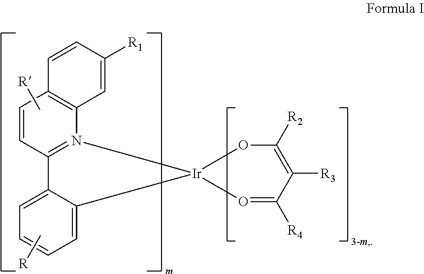
- In the compound of Formula I, R1 is selected from the group consisting of alkyl, cycloalkyl, heteroalkyl, aryl, heteroaryl, and combinations thereof, wherein R1 has four or more carbon atoms. R, R′, R2, R3 and R4 are independently selected from the group consisting of hydrogen, deuterium, halide, alkyl, cycloalkyl, heteroalkyl, arylalkyl, alkoxy, aryloxy, amino, silyl, alkenyl, cycloalkenyl, heteroalkenyl, alkynyl, aryl, heteroaryl, acyl, carbonyl, carboxylic acids, ester, nitrile, isonitrile, sulfonyl, sulfinyl, sulfonyl, phosphino, and combinations thereof. At least one of the R2, R3 and R4 has two or more carbon atoms, and R and R′ may represent mono, di, tri, tetra substitution, or no substitution. Two adjacent R, R2, R3, or R4 are optionally joined to form into a ring, and m is 1 or 2.
- In one aspect, the first device is a consumer product. In one aspect, the first device is an organic light-emitting device. In one aspect, the first device comprises a lighting panel.
- In one aspect, the organic layer further comprises a host. In one aspect, the host comprises a metal 8-hydroxyquinolate. In one aspect, the host is selected from the group consisting of:
-

- and combinations thereof.
-
FIG. 1 shows an organic light emitting device. -
FIG. 2 shows an inverted organic light emitting device that does not have a separate electron transport layer. -
FIG. 3 shows a compound of Formula I. - Generally, an OLED comprises at least one organic layer disposed between and electrically connected to an anode and a cathode. When a current is applied, the anode injects holes and the cathode injects electrons into the organic layer(s). The injected holes and electrons each migrate toward the oppositely charged electrode. When an electron and hole localize on the same molecule, an “exciton,” which is a localized electron-hole pair having an excited energy state, is formed. Light is emitted when the exciton relaxes via a photoemissive mechanism. In some cases, the exciton may be localized on an excimer or an exciplex. Non-radiative mechanisms, such as thermal relaxation, may also occur, but are generally considered undesirable.
- The initial OLEDs used emissive molecules that emitted light from their singlet states (“fluorescence”) as disclosed, for example, in U.S. Pat. No. 4,769,292, which is incorporated by reference in its entirety. Fluorescent emission generally occurs in a time frame of less than 10 nanoseconds.
- More recently, OLEDs having emissive materials that emit light from triplet states (“phosphorescence”) have been demonstrated. Baldo et al., “Highly Efficient Phosphorescent Emission from Organic Electraluminescent Devices,” Nature, vol. 395, 151-154, 1998; (“Baldo-I”) and Baldo et al., “Very high-efficiency green organic light-emitting devices based on electrophosphorescence,” Appl. Phys. Lett., vol. 75, No. 3, 4-6 (1999) (“Baldo-II”), which are incorporated by reference in their entireties. Phosphorescence is described in more detail in U.S. Pat. No. 7,279,704 at cols. 5-6, which are incorporated by reference.
-
FIG. 1 shows an organiclight emitting device 100. The figures are not necessarily drawn to scale.Device 100 may include asubstrate 110, ananode 115, ahole injection layer 120, ahole transport layer 125, anelectron blocking layer 130, anemissive layer 135, ahole blocking layer 140, anelectron transport layer 145, anelectron injection layer 150, aprotective layer 155, and acathode 160.Cathode 160 is a compound cathode having a firstconductive layer 162 and a secondconductive layer 164.Device 100 may be fabricated by depositing the layers described, in order. The properties and functions of these various layers, as well as example materials, are described in more detail in U.S. Pat. No. 7,279,704 at cols. 6-10, which are incorporated by reference. - More examples for each of these layers are available. For example, a flexible and transparent substrate-anode combination is disclosed in U.S. Pat. No. 5,844,363, which is incorporated by reference in its entirety. An example of a p-doped hole transport layer is m-MTDATA doped with F.sub.4-TCNQ at a molar ratio of 50:1, as disclosed in U.S. Patent Application Publication No. 2003/0230980, which is incorporated by reference in its entirety. Examples of emissive and host materials are disclosed in U.S. Pat. No. 6,303,238 to Thompson et al., which is incorporated by reference in its entirety. An example of an n-doped electron transport layer is BPhen doped with Li at a molar ratio of 1:1, as disclosed in U.S. Patent Application Publication No. 2003/0230980, which is incorporated by reference in its entirety. U.S. Pat. Nos. 5,703,436 and 5,707,745, which are incorporated by reference in their entireties, disclose examples of cathodes including compound cathodes having a thin layer of metal such as Mg:Ag with an overlying transparent, electrically-conductive, sputter-deposited ITO layer. The theory and use of blocking layers is described in more detail in U.S. Pat. No. 6,097,147 and U.S. Patent Application Publication No. 2003/0230980, which are incorporated by reference in their entireties. Examples of injection layers are provided in U.S. Patent Application Publication No. 2004/0174116, which is incorporated by reference in its entirety. A description of protective layers may be found in U.S. Patent Application Publication No. 2004/0174116, which is incorporated by reference in its entirety.
-
FIG. 2 shows aninverted OLED 200. The device includes asubstrate 210, acathode 215, anemissive layer 220, ahole transport layer 225, and ananode 230.Device 200 may be fabricated by depositing the layers described, in order. Because the most common OLED configuration has a cathode disposed over the anode, anddevice 200 hascathode 215 disposed underanode 230,device 200 may be referred to as an “inverted” OLED. Materials similar to those described with respect todevice 100 may be used in the corresponding layers ofdevice 200.FIG. 2 provides one example of how some layers may be omitted from the structure ofdevice 100. - The simple layered structure illustrated in
FIGS. 1 and 2 is provided by way of non-limiting example, and it is understood that embodiments of the invention may be used in connection with a wide variety of other structures. The specific materials and structures described are exemplary in nature, and other materials and structures may be used. Functional OLEDs may be achieved by combining the various layers described in different ways, or layers may be omitted entirely, based on design, performance, and cost factors. Other layers not specifically described may also be included. Materials other than those specifically described may be used. Although many of the examples provided herein describe various layers as comprising a single material, it is understood that combinations of materials, such as a mixture of host and dopant, or more generally a mixture, may be used. Also, the layers may have various sublayers. The names given to the various layers herein are not intended to be strictly limiting. For example, indevice 200,hole transport layer 225 transports holes and injects holes intoemissive layer 220, and may be described as a hole transport layer or a hole injection layer. In one embodiment, an OLED may be described as having an “organic layer” disposed between a cathode and an anode. This organic layer may comprise a single layer, or may further comprise multiple layers of different organic materials as described, for example, with respect toFIGS. 1 and 2 . - Structures and materials not specifically described may also be used, such as OLEDs comprised of polymeric materials (PLEDs) such as disclosed in U.S. Pat. No. 5,247,190 to Friend et al., which is incorporated by reference in its entirety. By way of further example, OLEDs having a single organic layer may be used. OLEDs may be stacked, for example as described in U.S. Pat. No. 5,707,745 to Forrest et al, which is incorporated by reference in its entirety. The OLED structure may deviate from the simple layered structure illustrated in
FIGS. 1 and 2 . For example, the substrate may include an angled reflective surface to improve out-coupling, such as a mesa structure as described in U.S. Pat. No. 6,091,195 to Forrest et al., and/or a pit structure as described in U.S. Pat. No. 5,834,893 to Bulovic et al., which are incorporated by reference in their entireties. - Unless otherwise specified, any of the layers of the various embodiments may be deposited by any suitable method. For the organic layers, preferred methods include thermal evaporation, ink-jet, such as described in U.S. Pat. Nos. 6,013,982 and 6,087,196, which are incorporated by reference in their entireties, organic vapor phase deposition (OVPD), such as described in U.S. Pat. No. 6,337,102 to Forrest et al., which is incorporated by reference in its entirety, and deposition by organic vapor jet printing (OVJP), such as described in U.S. patent application Ser. No. 10/233,470, which is incorporated by reference in its entirety. Other suitable deposition methods include spin coating and other solution based processes. Solution based processes are preferably carried out in nitrogen or an inert atmosphere. For the other layers, preferred methods include thermal evaporation. Preferred patterning methods include deposition through a mask, cold welding such as described in U.S. Pat. Nos. 6,294,398 and 6,468,819, which are incorporated by reference in their entireties, and patterning associated with some of the deposition methods such as ink jet and OVA). Other methods may also be used. The materials to be deposited may be modified to make them compatible with a particular deposition method. For example, substituents such as alkyl and aryl groups, branched or unbranched, and preferably containing at least 3 carbons, may be used in small molecules to enhance their ability to undergo solution processing. Substituents having 20 carbons or more may be used, and 3-20 carbons is a preferred range. Materials with asymmetric structures may have better solution processibility than those having symmetric structures, because asymmetric materials may have a lower tendency to recrystallize. Dendrimer substituents may be used to enhance the ability of small molecules to undergo solution processing.
- Devices fabricated in accordance with embodiments of the invention may be incorporated into a wide variety of consumer products, including flat panel displays, computer monitors, medical monitors, televisions, billboards, lights for interior or exterior illumination and/or signaling, heads up displays, fully transparent displays, flexible displays, laser printers, telephones, cell phones, personal digital assistants (PDAs), laptop computers, digital cameras, camcorders, viewfinders, micro-displays, vehicles, a large area wall, theater or stadium screen, or a sign. Various control mechanisms may be used to control devices fabricated in accordance with the present invention, including passive matrix and active matrix. Many of the devices are intended for use in a temperature range comfortable to humans, such as 18 degrees C. to 30 degrees C., and more preferably at room temperature (20-25 degrees C.).
- The materials and structures described herein may have applications in devices other than OLEDs. For example, other optoelectronic devices such as organic solar cells and organic photodetectors may employ the materials and structures. More generally, organic devices, such as organic transistors, may employ the materials and structures.
- The terms halo, halogen, alkyl, cycloalkyl, alkenyl, alkynyl, arylkyl, heterocyclic group, aryl, aromatic group, and heteroaryl are known to the art, and are defined in U.S. Pat. No. 7,279,704 at cols. 31-32, which are incorporated herein by reference.
- In one embodiment, a compound having the formula:
-
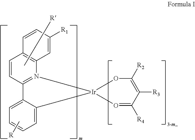
- is provided. In the compound of Formula I, R1 is selected from the group consisting of alkyl, cycloalkyl, heteroalkyl, aryl, heteroaryl, and combinations thereof, wherein R1 has four or more carbon atoms. R, R′, R2, R3 and R4 are independently selected from the group consisting of hydrogen, deuterium, halide, alkyl, cycloalkyl, heteroalkyl, arylalkyl, alkoxy, aryloxy, amino, silyl, alkenyl, cycloalkenyl, heteroalkenyl, alkenyl, aryl, heteroaryl, acyl, carbonyl, carboxylic acids, ester, nitrile, isonitrile, sulfanyl, sulfinyl, sulfonyl, phosphine, and combinations thereof. At least one of the R2, R3 and R4 has two or more carbon atoms, and R and R′ may represent mono, di, tri, tetra substitution, or no substitution. Two adjacent R, R2, R3, or R4 are optionally joined to form into a ring, and m is 1 or 2.
- As discussed below in the Device Example section, it has been unexpectedly discovered that when R1 is an alkyl group containing four or more carbons and at least one of R2-R4 has two or more carbons, that the resulting iridium complexes can be used to created OLED devices with superior properties. Compounds of Formula I are superior to compounds that have only R1 with four or more carbons or only at least one of R2-R4 has two or more carbons. The aforementioned substitution patter is believed to be synergistic. Without being bound by theory, the alkyl groups are believed to favorably affect the molecular packing in the crystal lattice of compounds of Formula I, such that when these compounds are used in OLED devices, the resulting devices have improved operational parameters such as increased luminance efficiency and narrow emission spectra.
- In one embodiment, the compound has the formula:
-

- In one embodiment, the compound has the formula:
-

- wherein R1 is selected from the group consisting of alkyl, cycloalkyl, and combinations thereof. In one embodiment, m is 2.
- In one embodiment, the compound has the formula:
-

- wherein R5 and R6 are alkyl.
- In one embodiment, the compound has the formula:
-

- In one embodiment, R2, R3, and R4 are independently selected from the group consisting of aryl, alkyl, hydrogen, deuterium, and combinations thereof. In another embodiment, R2, R3, and R4 are independently selected from the group consisting of: methyl, CH(CH3)2, CH2CH(CH3)2, phenyl, cyclohexyl, and combinations thereof.
- In one embodiment, R1 is alkyl. In one aspect, R1 is selected from the group consisting of: CH2CH(CH3)2, cyclopentyl, CH2C(CH3)3, and cyclohexyl. In one embodiment, R1 is CH2CH(CH3)2.
- In one embodiment, R3 is hydrogen or deuterium and R2 and R4 are independently selected from CH(CH3)2 and CH2CH(CH3)2.
- In one embodiment, the compound is selected from the group consisting of:
-


- In one aspect, a first device is provided. The first device comprises a first organic light emitting device, further comprising an anode, a cathode and an organic layer, disposed between the anode and the cathode, comprising a compound having the formula:
-

- In the compound of Formula I, RI is selected from the group consisting of alkyl, cycloalkyl, heteroalkyl, aryl, heteroaryl, and combinations thereof, wherein R1 has four or more carbon atoms. R, R′, R2, R3 and R4 are independently selected from the group consisting of hydrogen, deuterium, halide, alkyl, cycloalkyl, heteroalkyl, arylalkyl, alkoxy, aryloxy, amino, silyl, alkenyl, cycloalkenyl, heteroalkenyl, alkynyl, aryl, heteroaryl, acyl, carbonyl, carboxylic acids, ester, nitrile, isonitrile, sulfanyl, sulfanyl, sulfonyl, phosphino, and combinations thereof. At least one of the R2, R3 and R4 has two or more carbon atoms, and R and R′ may represent mono, di, ti, tetra substitution, or no substitution. Two adjacent R, R2, R3, or R4 are optionally joined to form into a ring, and m is 1 or 2.
- In one aspect, the first device is a consumer product. In one aspect, the first device is an organic light-emitting device. In one aspect, the first device comprises a lighting panel.
- In one aspect, the organic layer further comprises a host. In one aspect, the host comprises a metal 8-hydroxyquinolate. In one aspect, the host is selected from the group consisting of:
-
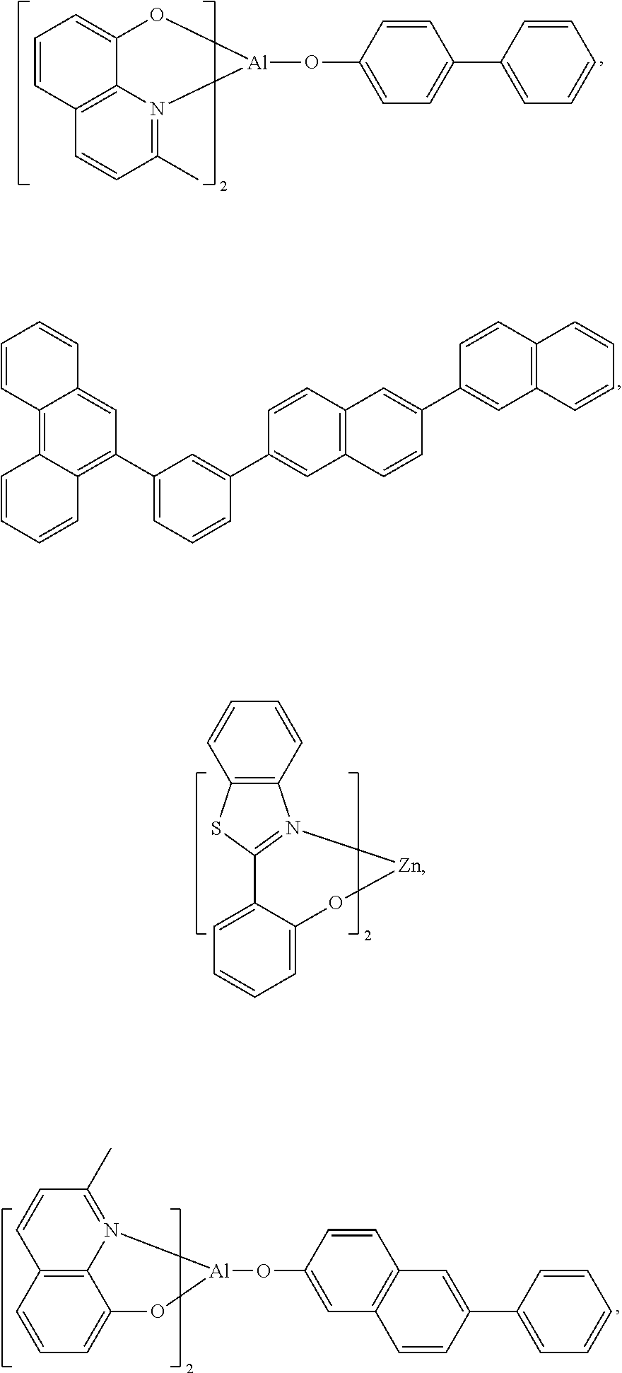
- and combinations thereof.
- All device examples were fabricated by high vacuum (<10−7 Torr) thermal evaporation (VTE). The anode electrode is 1200 Å of indium tin oxide (ITO). The cathode consisted of 10 Å of LiF followed by 1000 Å of Al. All devices were encapsulated with a glass lid sealed with an epoxy resin in a nitrogen glove box (<1 ppm of H2O and O2) immediately after fabrication, and a moisture getter was incorporated inside the package.
- The organic stack of the Device Example consisted of sequentially, from the ITO surface, 100 Å of hole injection layer (HIL), 300 Å of 4,4′-bis[N-(1-naphthyl)-N-phenylamino]biphenyl (α-NPD) as the hole transporting later (HTL), 300 Å of host doped with 9% of Compound 1 or 2 as the emissive layer (EML), and 400 Å of Alq3 (tris-8-hydroxyquinoline aluminum) as the ETL.
- As used herein, the following compounds have the following structures:
-

- The device structures are provided in Table 1, and the corresponding device data is provided in Table 2.
-
TABLE 1 VTE Phosphorescent OLEDs Device Example HIL HTL EML(doping %) ETL Example 1 Compound C NPD Compound D Compound Alq3 1 (9%) Example 2 Compound C NPD Compound D Compound Alq3 2 (9%) Comparative Compound C NPD Compound D Compound Alq3 Example 1 A (9%) Comparative Compound C NPD Compound D Compound Alq3 Example 2 B (9%) -
TABLE 2 VTE Device Data CIE At 1000 cd/m2 FWHM/ cd/A/ Device Example λmax nm CIE (x) CIE (y) V [V] cd/A EQE % lm/W EQE Example 1 612 52 0.652 0.346 7.5 28.9 21.2 12.0 1.36 Example 2 618 52 0.656 0.342 7.7 26.4 20.3 10.7 1.30 Comparative Example 1 616 60 0.656 0.342 8.4 26.2 20.8 9.8 1.26 Comparative Example 2 620 58 0.662 0.335 7.4 21.9 18.9 9.3 1.16 - It can be seen from Table 2 that the device examples containing compounds of Formula I, such as Compounds 1 and 2, show higher luminance efficiency and extremely narrow emission spectra versus the Comparative Examples 1 and 2, which have smaller alkyl groups on either the phenylquinoline or the acac-type ligand (acac is acetylacetone). Both Compound A and Compound 1 have a four carbon alkyl substituent on the 7-position of the heterocyclic ring. But, Compound A in Comparative Example 1 contains ligand
-

- where R2 and R4 are alkyl groups with one carbon atom.
- It has been unexpectedly discovered, that as the carbon chain length of R2 and R4 increases from one carbon to two or three carbons, the luminance efficiency increases and the FWHM (full width at half maximum) decreases in devices incorporating these longer carbon chains (i.e. compounds of Formula I). For example, using Compound 2 in Device Example 2, the luminance efficiency of Example 2 increases from 26.2 cd/A to 26.4 cd/A and the FWHM decreases from 60 nm to 52 nm. As the carbon chain length of R2 and R4 increases from three to four in Compound 1 in Device Example 1, the luminance of Device Example 1 increases to 28.9 cd/A and the FWHM is a narrow 52 nm. Furthermore, Comparative Example 2 contains Compound B which has the same acac-type ligand as in Compound 1 in device example 1. However, Compound B in Comparative Example 2 does not have any alkyl substitution on the 7 position of the heterocyclic ring with four or more carbons in the alkyl group, whereas Compound 1 does have such an alkyl group. The luminance efficiency of Compound 1 in Device Example 1 is 28.9 cd/A compared to 21.9 cd/A of Compound B in Comparative Example 2. Thus, unexpectedly, an iridium complex containing an acac-type ligand having alkyl substituents with two or more carbons and phenylquinoline ligand having an alkyl group with four or more carbons at the 7 position created a synergistic combination of properties that makes compounds of Formula I useful in OLED devices.
- Combination with Other Materials
- The materials described herein as useful for a particular layer in an organic light emitting device may be used in combination with a wide variety of other materials present in the device. For example, emissive dopants disclosed herein may be used in conjunction with a wide variety of hosts, transport layers, blocking layers, injection layers, electrodes and other layers that may be present. The materials described or referred to below are non-limiting examples of materials that may be useful in combination with the compounds disclosed herein, and one of skill in the art can readily consult the literature to identify other materials that may be useful in combination.
- A hole injecting/transporting material to be used in the present invention is not particularly limited, and any compound may be used as long as the compound is typically used as a hole injecting/transporting material. Examples of the material include, but not limit to: a phthalocyanine or porphryin derivative; an aromatic amine derivative; an indolocarbazole derivative; a polymer containing fluorohydrocarbon; a polymer with conductivity dopants; a conducting polymer, such as PEDOT/PSS; a self-assembly monomer derived from compounds such as phosphonic acid and sliane derivatives; a metal oxide derivative, such as MoOx; a p-type semiconducting organic compound, such as 1,4,5,8,9,12-Hexaazatriphenylenehexacarbonitrile; a metal complex, and a cross-linkable compounds.
- Examples of aromatic amine derivatives used in HIL or HTL include, but not limit to the following general structures:
-
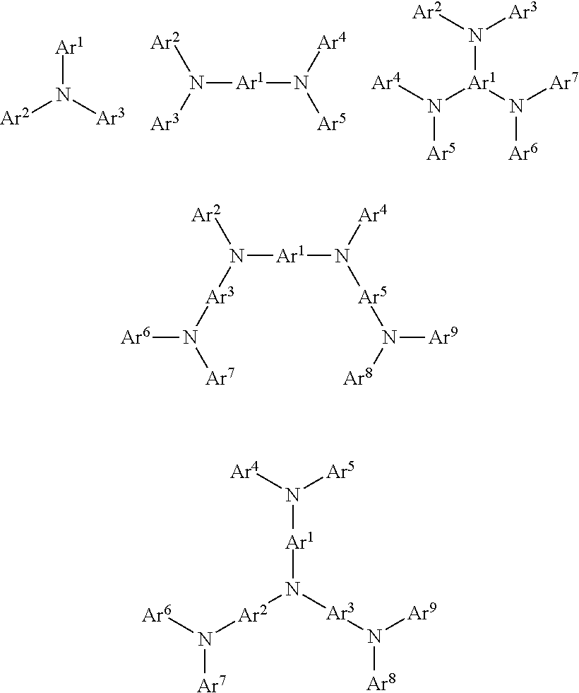
- Each of Ar1 to Ar9 is selected from the group consisting aromatic hydrocarbon cyclic compounds such as benzene, biphenyl, triphenyl, triphenylene, naphthalene, anthracene, phenalene, phenanthrene, fluorene, pyrene, cbrysene, perylene, azulene; group consisting aromatic heterocyclic compounds such as dibenzothiophene, dibenzofuran, dibenzoselenophene, furan, thiophene, benzofuran, benzothiophene, benzoselenophene, carbazole, indolocarbazole, pyridylindole, pyrrolodipyridine, pyrazole, imidazole, triazole, oxazole, thiazole, oxadiazole, oxatriazole, dioxazole, thiadiazole, pyridine, pyridazine, pyrimidine, pyrazine, triazine, oxazine, oxathiazine, oxadiazine, indole, benzimidazole, indazole, indoxazine, benzoxazole, benzisoxazole, benzothiazole, quinoline, isoquinoline, cinnoline, quinazoline, quinoxaline, naphthyridine, phthalazine, pteridine, xanthene, acridine, phenazine, phenothiazine, phenoxazine, benzofuropyridine, furodipyridine, benzothienopyridine, thienodipyridine, benzoselenophenopyridine, and selenophenodipyridine; and group consisting 2 to 10 cyclic structural units which are groups of the same type or different types selected from the aromatic hydrocarbon cyclic group and the aromatic heterocyclic group and are bonded to each other directly or via at least one of oxygen atom, nitrogen atom, sulfur atom, silicon atom, phosphorus atom, boron atom, chain structural unit and the aliphatic cyclic group. Wherein each Ar is further substituted by a substituent selected from the group consisting of hydrogen, deuterium, halide, alkyl, cycloalkyl, heteroalkyl, arylalkyl, alkoxy, aryloxy, amino, silyl, alkenyl, cycloalkenyl, heteroalkenyl, alkynyl, aryl, heteroaryl, acyl, carbonyl, carboxylic acids, ester, nitrile, isonitrile, sulfanyl, sulfinyl, sulfonyl, phosphino, and combinations thereof.
- In one aspect, Ar1 to Ar9 is independently selected from the group consisting of
-
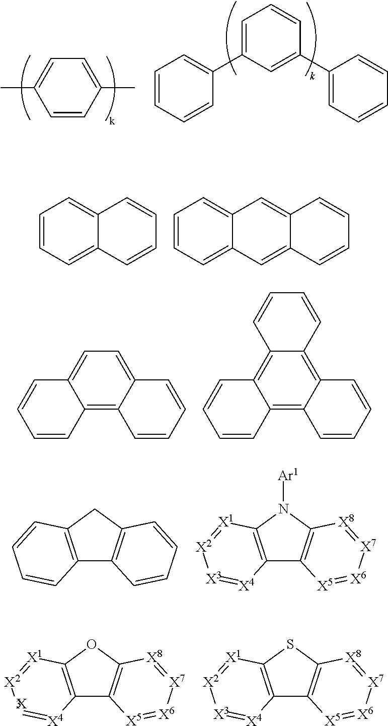
- k is an integer from 1 to 20; X1 to X8 is C (including CH) or N; Ar1 has the same group defined above.
- Examples of metal complexes used in HIL or HTL include, but not limit to the following general formula:
-

- M is a metal, having an atomic weight greater than 40; (Y1-Y2) is a bidentate ligand, Y1 and Y2 are independently selected from C, N, O, P, and S; L is an ancillary ligand; m is an integer value from 1 to the maximum number of ligands that may be attached to the metal; and m+n is the maximum number of ligands that may be attached to the metal.
- In one aspect, (Y1-Y2) is a 2-phenylpyridine derivative.
- In another aspect, (Y1-Y2) is a carbene ligand.
- In another aspect, M is selected from Ir, Pt, Os, and Zn.
- In a further aspect, the metal complex has a smallest oxidation potential in solution vs. Fc+/Fc couple less than about 0.6 V.
- The light emitting layer of the organic EL device of the present invention preferably contains at least a metal complex as light emitting material, and may contain a host material using the metal complex as a dopant material. Examples of the host material are not particularly limited, and any metal complexes or organic compounds may be used as long as the triplet energy of the host is larger than that of the dopant. While the Table below categorizes host materials as preferred for devices that emit various colors, any host material may be used with any dopant so long as the triplet criteria is satisfied.
- Examples of metal complexes used as host are preferred to have the following general formula:
-

- M is a metal; (Y3-Y4) is a bidentate ligand, Y3 and Y4 are independently selected from C, N, O, P, and S; L is an ancillary ligand; m is an integer value from 1 to the maximum number of ligands that may be attached to the metal; and m+n is the maximum number of ligands that may be attached to the metal.
- In one aspect, the metal complexes are:
-

- (O—N) is a bidentate ligand, having metal coordinated to atoms O and N.
- In another aspect, M is selected from Ir and Pt.
- In a further aspect, (Y3-Y4) is a carbene ligand.
- Examples of organic compounds used as host are selected from the group consisting aromatic hydrocarbon cyclic compounds such as benzene, biphenyl, triphenyl, triphenylene, naphthalene, anthracene, phenalene, phenanthrene, fluorene, pyrene, chrysene, perylene, azulene; group consisting aromatic heterocyclic compounds such as dibenzothiophene, dibenzofuran, dibenzoselenophene, furan, thiophene, benzofuran, benzothiophene, benzoselenophene, carbazole, indolocarbazole, pyridylindole, pyrrolodipyridine, pyrazole, imidazole, triazole, oxazole, thiazole, oxadiazole, oxatriazole, dioxazole, thiadiazole, pyridine, pyridazine, pyrimidine, pyrazine, triazine, oxazine, oxathiazine, oxadiazine, indole, benzimidazole, indazole, indoxazine, benzoxazole, benzisoxazole, benzothiazole, quinoline, isoquinoline, cinnoline, quinazoline, quinoxaline, naphthyridine, phthalazine, pteridine, xanthene, acridine, phenazine, phenothiazine, phenoxazine, benzofuropyridine, furodipyridine, benzothienopyridine, thienodipyridine, benzoselenophenopyridine, and selenophenodipyridine; and group consisting 2 to 10 cyclic structural units which are groups of the same type or different types selected from the aromatic hydrocarbon cyclic group and the aromatic heterocyclic group and are bonded to each other directly or via at least one of oxygen atom, nitrogen atome, sulfur atom, silicon atom, phosphorus atom, boron atom, chain structural unit and the aliphatic cyclic group. Wherein each group is further substituted by a substituent selected from the group consisting of hydrogen, deuterium, halide, alkyl, cycloalkyl, heteroalkyl, arylalkyl, alkoxy, aryloxy, amino, silyl, alkenyl, cycloalkenyl, heteroalkenyl, alkynyl, aryl, heteroaryl, acyl, carbonyl, carboxylic acids, ester, nitrile, isonitrile, sulfanyl, sulfanyl, sulfonyl, phosphino, and combinations thereof.
- In one aspect, host compound contains at least one of the following groups in the molecule:
-


- R1 to R7 is independently selected from the group consisting of hydrogen, deuterium, halide, alkyl, cycloalkyl, heteroalkyl, arylalkyl, alkoxy, aryloxy, amino, silyl, alkenyl, cycloalkenyl, heteroalkenyl, alkynyl, aryl, heteroaryl, acyl, carbonyl, carboxylic acids, ester, nitrile, isonitrile, sulfonyl, sulfnyl, sulfonyl, phosphino, and combinations thereof, when it is aryl or heteroaryl, it has the similar definition as Ar's mentioned above.
- k is an integer from 0 to 20.
- X1 to X8 is selected from C (including CH) or N.
- Z1 and Z2 is selected from NR1, O, or S.
- A hole blocking layer (HBL) may be used to reduce the number of holes and/or excitons that leave the emissive layer. The presence of such a blocking layer in a device may result in substantially higher efficiencies as compared to a similar device lacking a blocking layer. Also, a blocking layer may be used to confine emission to a desired region of an OLED.
- In one aspect, compound used in HBL contains the same molecule or the same functional groups used as host described above.
- In another aspect, compound used in HBL contains at least one of the following groups in the molecule:
-

- k is an integer from 0 to 20; L is an ancillary ligand, m is an integer from 1 to 3.
- Electron transport layer (ETL) may include a material capable of transporting electrons. Electron transport layer may be intrinsic (undoped), or doped. Doping may be used to enhance conductivity. Examples of the ETL material are not particularly limited, and any metal complexes or organic compounds may be used as long as they are typically used to transport electrons.
- In one aspect, compound used in ETL contains at least one of the following groups in the molecule:
-

- R1 is selected from the group consisting of hydrogen, deuterium, halide, alkyl, cycloalkyl, heteroalkyl, arylalkyl, alkoxy, aryloxy, amino, silyl, alkenyl, cycloalkenyl, heteroalkenyl, alkynyl, aryl, heteroaryl, acyl, carbonyl, carboxylic acids, ester, nitrile, isonitrile, sulfanyl, sulfinyl, sulfonyl, phosphino, and combinations thereof, when it is aryl or heteroaryl, it has the similar definition as Ar's mentioned above.
- Ar1 to Ar3 has the similar definition as Ar's mentioned above.
- k is an integer from 0 to 20.
- X1 to X5 is selected from C (including CH) or N.
- In another aspect, the metal complexes used in ETL contains, but not limit to the following general formula:
-

- (O—N) or (N—N) is a bidentate ligand, having metal coordinated to atoms O, N or N,N; L is an ancillary ligand; m is an integer value from 1 to the maximum number of ligands that may be attached to the metal.
- In any above-mentioned compounds used in each layer of the OLED device, the hydrogen atoms can be partially or fully deuterated.
- In addition to and/or in combination with the materials disclosed herein, many hole injection materials, hole transporting materials, host materials, dopant materials, exiton/hole blocking layer materials, electron transporting and electron injecting materials may be used in an OLED. Non-limiting examples of the materials that may be used in an OLED in combination with materials disclosed herein are listed in Table 3 below. Table 3 lists non-limiting classes of materials, non-limiting examples of compounds for each class, and references that disclose the materials.
-
TABLE 3 PUBLI- MATERIAL EXAMPLES OF MATERIAL CATIONS Hole injection materials Phthalo- cyanine and porphryin compounds 
Appl. Phys. Lett. 69, 2160 (1996) Starburst triarylamines 
J. Lumin. 72-74, 985 (1997) CFx Fluoro- hydrocarbon polymer 
Appl. Phys. Lett. 78, 673 (2001) Conducting polymers (e.g., PEDOT:PSS, polyaniline, poly- pthiophene) 
Synth. Met. 87, 171 (1997) WO2007002683 Phosphonic acid and sliane SAMs 
US20030162053 Triarylamine or polythiophene polymers with conductivity dopants 
EP1725079A1 

Organic compounds with conductive inorganic compounds, such as molybdenum and tungsten oxides 
US20050123751 SID Symposium Digest, 37, 923 (2006) WO2009018009 n-type semi- conducting organic complexes 
US20020158242 Metal organometallic complexes 
US20060240279 Cross-linkable compounds 
US20080220265 Polythiophene based polymers and copolymers 
WO2011075644 EP2350216 Hole transporting materials Triarylamines (e.g., TPD, α-NPD) 
Appl. Phys. Lett. 51, 913 (1987) 
U.S. Pat. No. 5,061,569 
EP650955 
J. Mater. Chem. 3, 319 (1993) 
Appl. Phys. Lett. 90, 183503 (2007) 
Appl. Phys. Lett. 90, 183503 (2007) Triaylamine on spiro- fluorene core 
Synth. Met. 91, 209 (1997) Arylamine carbazole compounds 
Adv. Mater. 6, 677 (1994), US20080124572 Triarylamine with (di)benzo- thiophene/ (di)benzofuran 
US20070278938, US20080106190 US20110163302 Indolo- carbazoles 
Synth. Met 111, 421 (2000) Isoindole compounds 
Chem. Mater. 15, 3148 (2003) Metal carbene complexes 
US20080018221 Phosphorescent OLED host materials Red hosts Aryl- carbazoles 
Appl. Phys. Lett. 78, 1622 (2001) Metal 8-hydroxy- quinolates (e.g., Alq3, BAlq) 
Nature 395, 151 (1998) 
US20060202194 
WO2005014551 
WO2006072002 Metal phenoxy- benzothiazole compounds 
Appl. Phys. Lett. 90, 123509 (2007) Conjugated oligomers and polymers (e.g., poly- fluorene) 
Org. Electron, 1, 15 (2000) Aromatic fused rings 
WO2009066779, WO2009066778, WO2009063833, US20090045731, US20090045730, WO2009008311, US20090008605, US20090009065 Zinc complexes 
WO2010056066 Chrysene based compounds 
WO2011086863 Green hosts Aryl- carbazoles 
Appl. Phys. Lett. 78, 1622 (2001) 
US20030175553 
WO2001039234 Aryltri- phenylene compounds 
US20060280965 
US20060280965 
WO2009021126 Poly-fused heteroaryl compounds 
US20090309488 US20090302743 US20100012931 Donor acceptor type molecules 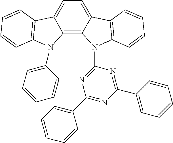
WO2008056746 
WO2010107244 Aza-carbazole/ DBT/DBF 
JP2008074939 
US20100187984 Polymers (e.g., PVK) 
Appl. Phys. Lett. 77, 2280 (2000) Spirofluorene compounds 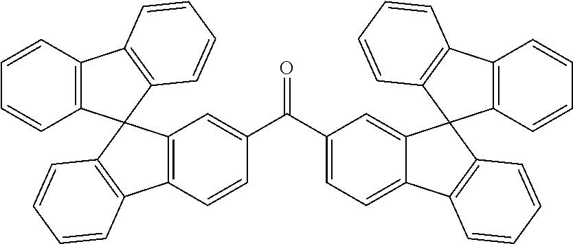
WO2004093207 Metal phenoxy- benzooxazole compounds 
WO2005089025 
WO2006132173 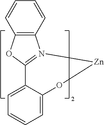
JP200511610 Spirofluorene- carbazole compounds 
JP2007254297 
JP2007254297 Indolo- cabazoles 
WO2007063796 
WO2007063754 5-member ring electron deficient heterocycles (e.g., triazole, oxadiazole) 
J. Appl. Phys. 90, 5048 (2001) 
WO2004107822 Tetra- phenylene complexes 
US20050112407 Metal phenoxy- pyridine compounds 
WO2005030900 Metal coordination complexes (e.g., Zn, Al with N{circumflex over ( )}N ligands) 
US20040137268, US20040137267 Blue hosts Aryl- carbazoles 
Appl. Phys. Lett, 82, 2422 (2003) 
US20070190359 Dibenzo- thiophene/ Dibenzofuran- carbazole compounds 
WO2006114966, US20090167162 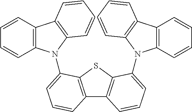
US20090167162 
WO2009086028 
US20090030202, US20090017330 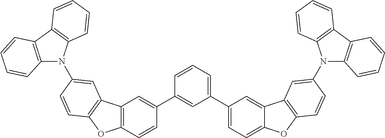
US20100084966 Silicon aryl compounds 
US20050238919 
WO2009003898 Silicon/ Germanium aryl compounds 
EP2034538A Aryl benzoyl ester 
WO2006100298 Carbazole linked by non- conjugated groups 
US20040115476 Aza- carbazoles 
US20060121308 High triplet metal organometallic complex 
U.S. Pat. No. 7,154,114 Phosphorescent dopants Red dopants Heavy metal porphyrins (e.g., PtOEP) 
Nature 395, 151 (1998) Iridium (III) organometallic complexes 
Appl. Phys. Lett. 78, 1622 (2001) 
US2006835469 
US2006835469 
US20060202194 
US20060202194 
US20070087321 
US20080261076 US20100090591 
US20070087321 
Adv. Mater. 19, 739 (2007) 
WO2009100991 
WO2008101842 
U.S. Pat. No. 7,232,618 Platinum (II) organometallic complexes 
WO2003040257 
US20070103060 Osminum (III) complexes 
Chem. Mater. 17, 3532 (2005) Ruthenium (II) complexes 
Adv. Mater. 17, 1059 (2005) Rhenium (I), (II), and (III) complexes 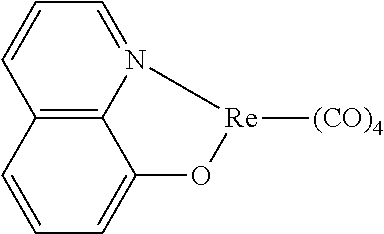
US20050244673 Green dopants Iridium (III) organometallic complexes 
Inorg. Chem. 40, 1704 (2001) 
US20020034656 
U.S. Pat. No. 7,332,232 
US20090108737 
WO2010028151 
EP1841834B 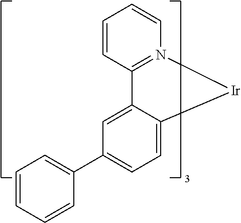
US20060127696 
US20090039776 
U.S. Pat. No. 6,921,915 
US20100244004 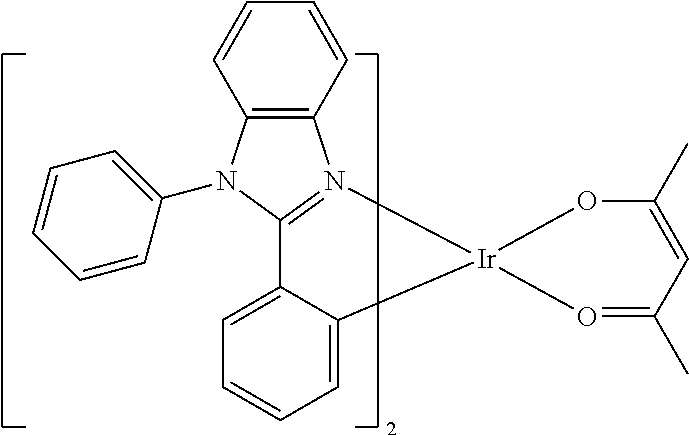
U.S. Pat. No. 6,687,266 
Chem. Mater. 16, 2480 (2004) 
US20070190359 
US20060008670 JP2007123392 
WO2010086089, WO2011044988 
Adv. Mater. 16, 2003 (2004) 
Angew. Chem. Int. Ed. 2006, 45, 7800 
WO2009050290 
US20090165846 
US20080015355 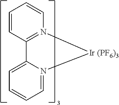
US20010015432 
US20100295032 Monomer for polymeric metal organometallic compounds 
U.S. Pat. No. 7,250,226, U.S. Pat. No. 7,396,598 Pt (II) organometallic complexes, including polydentated ligands 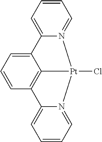
Appl. Phys. Lett. 86, 153505 (2005) 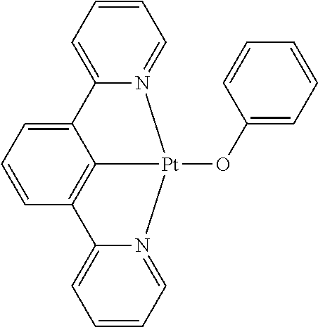
Appl. Phys. Lett. 86, 153505 (2005) 
Chem. Lett. 34, 592 (2005) 
WO2002015645 
US20060263635 
US20060182992 US20070103060 Cu complexes 
WO2009000673 
US20070111026 Gold complexes 
Chem. Commun. 2906 (2005) Rhenium (III) complexes 
Inorg. Chem. 42, 1248 (2003) Osmium (II) complexes 
U.S. Pat. No. 7,279,704 Deuterated organometallic complexes 
US20030138657 Organometallic complexes with two or more metal centers 
US20030152802 
U.S. Pat. No. 7,090,928 Blue dopants Iridium (III) organometallic complexes 
WO2002002714 
WO2006009024 
US20060251923 US20110057559 US20110204333 
U.S. Pat. No. 7,393,599, WO2006056418, US20050260441, WO2005019373 
U.S. Pat. No. 7,534,505 
WO2011051404 
U.S. Pat. No. 7,445,855 
US20070190359, US20080297033 US20100148663 
U.S. Pat. No. 7,338,722 
US20020134984 
Angew. Chem. Int. Ed. 47, 1 (2008) 
Chem. Mater. 18, 5119 (2006) 
Inorg. Chem. 46, 4308 (2007) 
WO2005123873 
WO2005123873 
WO2007004380 
WO2006082742 Osmium (II) complexes 
U.S. Pat. No. 7,279,704 
Organo- metallics 23, 3745 (2004) Gold complexes 
Appl. Phys. Lett. 74, 1361 (1999) Platinum (II) complexes 
WO2006098120, WO2006103874 Pt tetradentate complexes with at least one metal-carbene bond 
U.S. Pat. No. 7,655,323 Exciton/hole blocking layer materials Bathocuprine compounds (e.g., BCP, BPhen) 
Appl. Phys. Lett. 75, 4 (1999) 
Appl. Phys. Lett. 79, 449 (2001) Metal 8-hydroxy- quinolates (e.g., BAlq) 
Appl. Phys. Lett. 81, 162 (2002) 5-member ring electron deficient heterocycles such as triazole, oxadiazole, imidazole, benzo- imidazole 
Appl. Phys. Lett. 81, 162 (2002) Triphenylene compounds 
US20050025993 Fluorinated aromatic compounds 
Appl. Phys. Lett. 79, 156 (2001) Phenothiazine- S-oxide 
WO2008132085 Silylated five-membered nitrogen, oxygen, sulfur or phosphorus dibenzo- heterocycles 
WO2010079051 Aza- carbazoles 
US20060121308 Electron transporting materials Anthracene- benzo- imidazole compounds 
WO2003060956 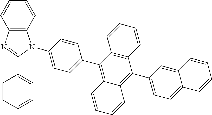
US20090179554 Aza triphenylene derivatives 
US20090115316 Anthracene- benzothiazole compounds 
Appl. Phys. Lett. 89, 063504 (2006) Metal 8-hydroxy- quinolates (e.g., Alq3, Zrq4) 
Appl. Phys. Lett. 51, 913 (1987) U.S. Pat. No. 7,230,107 Metal hydroxy- benoquinolates 
Chem. Lett. 5, 905 (1993) Bathocuprine compounds such as BCP, BPhen, etc 
Appl. Phys. Lett. 91, 263503 (2007) 
Appl. Phys. Lett. 79, 449 (2001) 5-member ring electron deficient heterocycles (e.g., triazole, oxadiazole, imidazole, benzo- imidazole) 
Appl. Phys. Lett. 74, 865 (1999) 
Appl. Phys. Lett. 55, 1489 (1989) 
Jpn. J. Apply. Phys. 32, L917 (1993) Silole compounds 
Org. Electron. 4, 113 (2003) Arylborane compounds 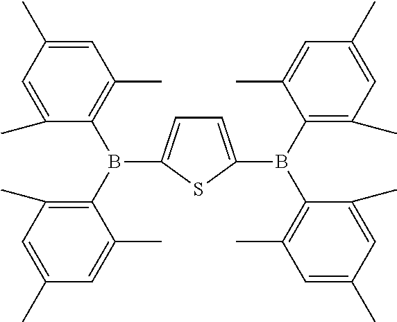
J. Am. Chem. Soc. 120, 9714 (1998) Fluorinated aromatic compounds 
J. Am. Chem. Soc 122, 1832 (2000) Fullerene (e.g., C60) 
US20090101870 Triazine complexes 
US20040036077 Zn (N{circumflex over ( )}N) complexes 
U.S. Pat. No. 6,528,187 
- Chemical abbreviations used throughout this document are as follows: Cy is cyclohexyl, dba is dibenzylideneacetone, EtOAc is ethyl acetate, DME is dimethoxyethane, dppe is 1,2-bis(diphenylphosphino)ethane, THF is tetrahydrofuran, DCM is dichloromethane, S-Phos is dicyclohexyl(2′,6′-dimethoxy-[1,1′-biphenyl]-2-yl)phosphine.
- Synthesis of Compound 1
- Step 1
-

- 2-Amino-4-clorobenzoic acid (42.8 g, 0.25 mol) was dissolved in 200 mL of anhydrous THF and cooled in an ice-water bath. To the solution was added lithium aluminum hydride chips (11.76 g, 0.31 mol). The resulting mixture was stirred at room temperature for 8 hours. Water (12 mL) was added, and then 12g 15% NaOH, followed by an additional 36 mL of water. The slurry was stirred at room temperature for 30 minutes then filtered. The filtered solid was washed with ethyl acetate. The liquid was combined and the solvent was evaporated to produce crude material, which was used in the next step without purification.
- Step 2
-

- 2-Amino-4-chlorophenylmethanol (6.6 g, 0.04 mol), dimethylphenyl)ethanone (10.0 g, 0.068 mol), RuCl2(PPh3)3 (0.1 g, 12 mmol) and 2.4 g (0.043 mol) of KOH was refluxed in 100 mL of toluene for 10 hours. Water was collected from the reaction using a Dean-Stark trap. After the reaction was cooled to room temperature, the mixture was filtered through a silica gel plug. The product was further purified with column chromatography using 2% ethyl acetate in hexanes as eluent, to obtain 9 g of product. The product after chromatography was further recrystallized from isopropanol to produce 5 g (50%) of the desired product.
-
Step 3 -
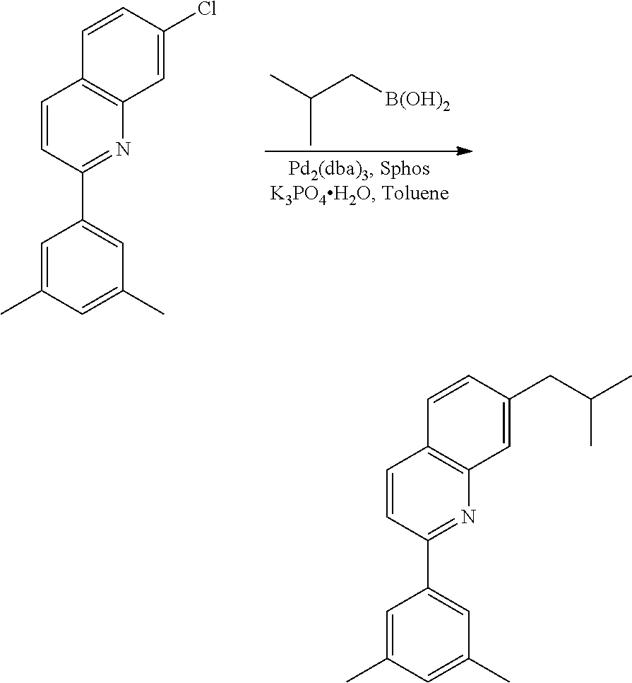
- 7-Chloro-2-(3,5-dimethylphenyl)quinoline (3.75 g, 0.014 mol), isobutylboronic acid (2.8 g, 0.028 mol), Pd2(dba)3 (1 mol %), 2-dicyclohexylphosphino-2′,6′-dimethoxybiphenyl (5-Phos) (4 mol %), potassium phosphate monohydrate (16.0 g) and 100 mL of toluene was charged in a 250 mL round bottom flask. Nitrogen was bubbled through the reaction mixture for 20 minutes and the mixture was heated to reflux for 18 hours overnight. The reaction mixture was allowed to cool to ambient temperature and the crude product was purified by column chromatography using 2% ethyl acetate in hexanes as solvent to obtain 3.6 g (90%) of desired product after evaporation of solvent.
- Step 4
-

- The ligand from step 3 (4.6 g, 16 mmol), 2-ethoxyethanol (25 mL) and water (5 mL) were charged in a IL three-neck round bottom flask. Nitrogen gas was bubbled through the reaction mixture 45 minutes. IrCl3.H2O (1.2 g, 3.6 mmol) was then added and the reaction mixture was heated to reflux under nitrogen for 17 hours. The reaction mixture was cooled to room temperature and filtered. The dark red residue was washed with methanol (2×25 mL) followed by hexanes (2×25 mL) to obtain 1.3 g (87%) of the dichlorobridged iridium dimer after drying in a vacuum oven.
- Step 5
-

- N,N dimethylformamide (DMF) (1 L) and potassium tert-butoxide (135.0 g 1.2 mol) were heated to 50° C. under nitrogen. Methyl 3-methylbutanoate (86.0 g, 0.75 mol) was added dropwise from a dropping funnel followed by a solution of 4-methylpentane-2-one (50 g, 1 mol) in 100 mL DMF. The progress of the reaction was monitored by GC. When the reaction was completed, the mixture was cooled to room temperature and slowly neutralized with 20% H2SO4 solution. Water (300 mL) was added and two layers formed. The layer containing the 2,8-dimethylnonane-4,6-dione was purified using vacuum distillation to give 40 g (43% yield) of a pink oil.
- Step 6
-

- The dichlorobridged iridium dimer from step 4 (1.0 g, 0.6 mmol), 2,8-dimethylnonane-4,6-dione (0.8 g, 6 mmol), Na2CO3 (3 g, 12 mmol) and 25 mL of 2-ethoxyethanol were placed in a 250 mL round bottom flask. The reaction mixture was stirred at room temperature for 24 hours, after which 2 g of Celite® and 200 mL of dichloromethane was added to the reaction mixture to dissolve the product. The mixture was filtered through a bed of Celite®. The filtrate was passed through a through a silica/alumina plug and washed with dichloromethane. The clarified solution was filtered through GF/F filter paper, and the filtrate was heated to remove most of the dichloromethane. Isopropanol (20 mL) was then added and the slurry was cooled to room temperature and the product was filtered and washed with isopropanol and dried to give 1.1 g (97% yield) of crude product. This product was recrystallized twice from dichloromethane and then sublimed to obtain Compound 1.
- Synthesis of Compound 2.
-

- Dichlorobridged iridium dimer from step 4 from the previous synthesis (2.75 g, 1.71 mmol), 2,6-dimethylheptane-3,5-dione (2.67 g, 17.1 mmol), K2CO3 (2.3 g, 34.2 mmol) and 25 mL of 2-ethoxyethanol were placed in a 250 mL round bottom flask. The reaction mixture was stirred at ambient for 24 hours, after which. 2 g of Celite® and 200 mL of dichloromethane was added to the reaction mixture to dissolve the product. The mixture was filtered through a bed of Celite®. The filtrate was passed through a through a silica/alumina plug and washed with dichloromethane. The clarified solution was then filtered through GF/F filter paper, and the filtrate was heated to remove most of the dichloromethane. Isopropanol (20 mL) was then added and the slurry was cooled to room temperature and the product was filtered and washed with isopropanol and dried to give 1.49 g (97% yield) of crude product. This product was then recrystallized twice and then sublimed to obtain Compound 2.
- It is understood that the various embodiments described herein are by way of example only, and are not intended to limit the scope of the invention. For example, many of the materials and structures described herein may be substituted with other materials and structures without deviating from the spirit of the invention. The present invention as claimed may therefore include variations from the particular examples and preferred embodiments described herein, as will be apparent to one of skill in the art. It is understood that various theories as to why the invention works are not intended to be limiting.
Claims (20)


Priority Applications (5)
| Application Number | Priority Date | Filing Date | Title |
|---|---|---|---|
| US13/345,285 US9163174B2 (en) | 2012-01-04 | 2012-01-06 | Highly efficient phosphorescent materials |
| KR1020130000225A KR102012047B1 (en) | 2012-01-06 | 2013-01-02 | Highly efficient phosphorescent materials |
| JP2013000115A JP6062741B2 (en) | 2012-01-06 | 2013-01-04 | High efficiency phosphorescent material |
| DE102013200085.5A DE102013200085B4 (en) | 2012-01-06 | 2013-01-07 | Highly efficient phosphorescent materials |
| JP2016210603A JP6473437B2 (en) | 2012-01-04 | 2016-10-27 | High efficiency phosphorescent material |
Applications Claiming Priority (2)
| Application Number | Priority Date | Filing Date | Title |
|---|---|---|---|
| US201261583045P | 2012-01-04 | 2012-01-04 | |
| US13/345,285 US9163174B2 (en) | 2012-01-04 | 2012-01-06 | Highly efficient phosphorescent materials |
Publications (2)
| Publication Number | Publication Date |
|---|---|
| US20130169148A1 true US20130169148A1 (en) | 2013-07-04 |
| US9163174B2 US9163174B2 (en) | 2015-10-20 |
Family
ID=48694286
Family Applications (1)
| Application Number | Title | Priority Date | Filing Date |
|---|---|---|---|
| US13/345,285 Active 2034-08-14 US9163174B2 (en) | 2012-01-04 | 2012-01-06 | Highly efficient phosphorescent materials |
Country Status (2)
| Country | Link |
|---|---|
| US (1) | US9163174B2 (en) |
| JP (1) | JP6473437B2 (en) |
Cited By (5)
| Publication number | Priority date | Publication date | Assignee | Title |
|---|---|---|---|---|
| CN105295895A (en) * | 2014-07-22 | 2016-02-03 | 环球展览公司 | Organic electroluminescent material and device |
| EP3040396A1 (en) * | 2014-12-30 | 2016-07-06 | Universal Display Corporation | Organic electroluminescent materials and devices |
| CN106892865A (en) * | 2015-12-19 | 2017-06-27 | 西安瑞联新材料股份有限公司 | A kind of synthetic method of the chloro- 6- p-methylphenyls quinoline of 2,4- bis- |
| US9991454B2 (en) | 2014-12-16 | 2018-06-05 | Samsung Display Co., Ltd. | Organometallic compound and organic light-emitting device including the same |
| US11390639B2 (en) * | 2018-04-13 | 2022-07-19 | Universal Display Corporation | Organic electroluminescent materials and devices |
Families Citing this family (2)
| Publication number | Priority date | Publication date | Assignee | Title |
|---|---|---|---|---|
| US10199581B2 (en) * | 2013-07-01 | 2019-02-05 | Universal Display Corporation | Organic electroluminescent materials and devices |
| US10535821B2 (en) | 2016-12-13 | 2020-01-14 | International Business Machines Corporation | Small molecule acceptors derived from renewable furan source |
Citations (4)
| Publication number | Priority date | Publication date | Assignee | Title |
|---|---|---|---|---|
| US20090085476A1 (en) * | 2007-09-27 | 2009-04-02 | Chun Gun Park | Red phosphorescent compound and organic electroluminescent device using the same |
| US20100102714A1 (en) * | 2008-10-29 | 2010-04-29 | Jung-Keun Kim | Red phosphorescent compound and organic electroluminescent device using the same |
| US20120181511A1 (en) * | 2011-01-13 | 2012-07-19 | Universal Display Corporation | 5-Substituted 2 Phenylquinoline Complexes Materials for Light Emitting Diode |
| US20130126831A1 (en) * | 2011-11-21 | 2013-05-23 | Universal Display Corporation | Organic light emitting materials |
Family Cites Families (124)
| Publication number | Priority date | Publication date | Assignee | Title |
|---|---|---|---|---|
| US4769292A (en) | 1987-03-02 | 1988-09-06 | Eastman Kodak Company | Electroluminescent device with modified thin film luminescent zone |
| GB8909011D0 (en) | 1989-04-20 | 1989-06-07 | Friend Richard H | Electroluminescent devices |
| US5061569A (en) | 1990-07-26 | 1991-10-29 | Eastman Kodak Company | Electroluminescent device with organic electroluminescent medium |
| DE69412567T2 (en) | 1993-11-01 | 1999-02-04 | Hodogaya Chemical Co., Ltd., Tokio/Tokyo | Amine compound and electroluminescent device containing it |
| US5707745A (en) | 1994-12-13 | 1998-01-13 | The Trustees Of Princeton University | Multicolor organic light emitting devices |
| US5703436A (en) | 1994-12-13 | 1997-12-30 | The Trustees Of Princeton University | Transparent contacts for organic devices |
| US6939625B2 (en) | 1996-06-25 | 2005-09-06 | Nôrthwestern University | Organic light-emitting diodes and methods for assembly and enhanced charge injection |
| US5844363A (en) | 1997-01-23 | 1998-12-01 | The Trustees Of Princeton Univ. | Vacuum deposited, non-polymeric flexible organic light emitting devices |
| US6091195A (en) | 1997-02-03 | 2000-07-18 | The Trustees Of Princeton University | Displays having mesa pixel configuration |
| US6013982A (en) | 1996-12-23 | 2000-01-11 | The Trustees Of Princeton University | Multicolor display devices |
| US5834893A (en) | 1996-12-23 | 1998-11-10 | The Trustees Of Princeton University | High efficiency organic light emitting devices with light directing structures |
| US6303238B1 (en) | 1997-12-01 | 2001-10-16 | The Trustees Of Princeton University | OLEDs doped with phosphorescent compounds |
| US6337102B1 (en) | 1997-11-17 | 2002-01-08 | The Trustees Of Princeton University | Low pressure vapor phase deposition of organic thin films |
| US6087196A (en) | 1998-01-30 | 2000-07-11 | The Trustees Of Princeton University | Fabrication of organic semiconductor devices using ink jet printing |
| US6528187B1 (en) | 1998-09-08 | 2003-03-04 | Fuji Photo Film Co., Ltd. | Material for luminescence element and luminescence element using the same |
| US6830828B2 (en) | 1998-09-14 | 2004-12-14 | The Trustees Of Princeton University | Organometallic complexes as phosphorescent emitters in organic LEDs |
| US6097147A (en) | 1998-09-14 | 2000-08-01 | The Trustees Of Princeton University | Structure for high efficiency electroluminescent device |
| US6294398B1 (en) | 1999-11-23 | 2001-09-25 | The Trustees Of Princeton University | Method for patterning devices |
| US6458475B1 (en) | 1999-11-24 | 2002-10-01 | The Trustee Of Princeton University | Organic light emitting diode having a blue phosphorescent molecule as an emitter |
| KR100377321B1 (en) | 1999-12-31 | 2003-03-26 | 주식회사 엘지화학 | Electronic device comprising organic compound having p-type semiconducting characteristics |
| US20020121638A1 (en) | 2000-06-30 | 2002-09-05 | Vladimir Grushin | Electroluminescent iridium compounds with fluorinated phenylpyridines, phenylpyrimidines, and phenylquinolines and devices made with such compounds |
| CN101924190B (en) | 2000-08-11 | 2012-07-04 | 普林斯顿大学理事会 | Organometallic compounds and emission-shifting organic electrophosphorescence |
| US6579630B2 (en) | 2000-12-07 | 2003-06-17 | Canon Kabushiki Kaisha | Deuterated semiconducting organic compounds used for opto-electronic devices |
| JP3812730B2 (en) | 2001-02-01 | 2006-08-23 | 富士写真フイルム株式会社 | Transition metal complex and light emitting device |
| JP4307000B2 (en) | 2001-03-08 | 2009-08-05 | キヤノン株式会社 | Metal coordination compound, electroluminescent element and display device |
| JP4310077B2 (en) | 2001-06-19 | 2009-08-05 | キヤノン株式会社 | Metal coordination compound and organic light emitting device |
| CN100440568C (en) | 2001-06-20 | 2008-12-03 | 昭和电工株式会社 | Light-emitting materials and organic light-emitting devices |
| US7071615B2 (en) | 2001-08-20 | 2006-07-04 | Universal Display Corporation | Transparent electrodes |
| US7250226B2 (en) | 2001-08-31 | 2007-07-31 | Nippon Hoso Kyokai | Phosphorescent compound, a phosphorescent composition and an organic light-emitting device |
| US7431968B1 (en) | 2001-09-04 | 2008-10-07 | The Trustees Of Princeton University | Process and apparatus for organic vapor jet deposition |
| US6835469B2 (en) | 2001-10-17 | 2004-12-28 | The University Of Southern California | Phosphorescent compounds and devices comprising the same |
| US7166368B2 (en) | 2001-11-07 | 2007-01-23 | E. I. Du Pont De Nemours And Company | Electroluminescent platinum compounds and devices made with such compounds |
| US6863997B2 (en) | 2001-12-28 | 2005-03-08 | The Trustees Of Princeton University | White light emitting OLEDs from combined monomer and aggregate emission |
| KR100691543B1 (en) | 2002-01-18 | 2007-03-09 | 주식회사 엘지화학 | New material for electron transport and organic light emitting device using the same |
| US20030230980A1 (en) | 2002-06-18 | 2003-12-18 | Forrest Stephen R | Very low voltage, high efficiency phosphorescent oled in a p-i-n structure |
| US7189989B2 (en) | 2002-08-22 | 2007-03-13 | Fuji Photo Film Co., Ltd. | Light emitting element |
| KR100686268B1 (en) | 2002-08-27 | 2007-02-28 | 후지필름 가부시키가이샤 | Organometallic Complex, Organic EL Element, and Organic EL Display |
| US6687266B1 (en) | 2002-11-08 | 2004-02-03 | Universal Display Corporation | Organic light emitting materials and devices |
| JP4365196B2 (en) | 2002-12-27 | 2009-11-18 | 富士フイルム株式会社 | Organic electroluminescence device |
| JP4365199B2 (en) | 2002-12-27 | 2009-11-18 | 富士フイルム株式会社 | Organic electroluminescence device |
| EP1606296B1 (en) | 2003-03-24 | 2009-08-05 | University Of Southern California | PHENYL-PYRAZOLE COMPLEXES OF Ir |
| US7090928B2 (en) | 2003-04-01 | 2006-08-15 | The University Of Southern California | Binuclear compounds |
| JP5318347B2 (en) | 2003-04-15 | 2013-10-16 | メルク パテント ゲーエムベーハー | Mixture of matrix material and organic semiconductor capable of emitting light, use thereof, and electronic component comprising said mixture |
| US7029765B2 (en) | 2003-04-22 | 2006-04-18 | Universal Display Corporation | Organic light emitting devices having reduced pixel shrinkage |
| JP4673744B2 (en) | 2003-05-29 | 2011-04-20 | 新日鐵化学株式会社 | Organic electroluminescence device |
| US20050025993A1 (en) | 2003-07-25 | 2005-02-03 | Thompson Mark E. | Materials and structures for enhancing the performance of organic light emitting devices |
| US7485706B2 (en) | 2003-07-30 | 2009-02-03 | The Board Of Trustees Of The Leland Stanford Junior University | Neurodegenerative protein aggregation inhibition methods and compounds |
| TWI390006B (en) | 2003-08-07 | 2013-03-21 | Nippon Steel Chemical Co | Organic EL materials with aluminum clamps |
| DE10338550A1 (en) | 2003-08-19 | 2005-03-31 | Basf Ag | Transition metal complexes with carbene ligands as emitters for organic light-emitting diodes (OLEDs) |
| US20060269780A1 (en) | 2003-09-25 | 2006-11-30 | Takayuki Fukumatsu | Organic electroluminescent device |
| JP4822687B2 (en) | 2003-11-21 | 2011-11-24 | 富士フイルム株式会社 | Organic electroluminescence device |
| US7332232B2 (en) | 2004-02-03 | 2008-02-19 | Universal Display Corporation | OLEDs utilizing multidentate ligand systems |
| WO2005089024A1 (en) | 2004-03-11 | 2005-09-22 | Mitsubishi Chemical Corporation | Composition for charge-transporting film and ion compound, charge-transporting film and organic electroluminescent device using same, and method for manufacturing organic electroluminescent device and method for producing charge-transporting film |
| TW200531592A (en) | 2004-03-15 | 2005-09-16 | Nippon Steel Chemical Co | Organic electroluminescent device |
| JP4869565B2 (en) | 2004-04-23 | 2012-02-08 | 富士フイルム株式会社 | Organic electroluminescence device |
| US7491823B2 (en) | 2004-05-18 | 2009-02-17 | The University Of Southern California | Luminescent compounds with carbene ligands |
| US7279704B2 (en) | 2004-05-18 | 2007-10-09 | The University Of Southern California | Complexes with tridentate ligands |
| US7445855B2 (en) | 2004-05-18 | 2008-11-04 | The University Of Southern California | Cationic metal-carbene complexes |
| US7534505B2 (en) | 2004-05-18 | 2009-05-19 | The University Of Southern California | Organometallic compounds for use in electroluminescent devices |
| US7154114B2 (en) | 2004-05-18 | 2006-12-26 | Universal Display Corporation | Cyclometallated iridium carbene complexes for use as hosts |
| US7393599B2 (en) | 2004-05-18 | 2008-07-01 | The University Of Southern California | Luminescent compounds with carbene ligands |
| WO2005123873A1 (en) | 2004-06-17 | 2005-12-29 | Konica Minolta Holdings, Inc. | Organic electroluminescent device material, organic electroluminescent device, display and illuminating device |
| CA2568667A1 (en) | 2004-06-28 | 2006-01-05 | Ciba Specialty Chemicals Holding Inc. | Electroluminescent metal complexes with triazoles and benzotriazoles |
| US20060008670A1 (en) | 2004-07-06 | 2006-01-12 | Chun Lin | Organic light emitting materials and devices |
| EP2178348B1 (en) | 2004-07-23 | 2012-11-21 | Konica Minolta Holdings, Inc. | Organic electroluminescent element, display and illuminator |
| DE102004057072A1 (en) | 2004-11-25 | 2006-06-01 | Basf Ag | Use of Transition Metal Carbene Complexes in Organic Light Emitting Diodes (OLEDs) |
| KR101272435B1 (en) | 2004-12-30 | 2013-06-07 | 이 아이 듀폰 디 네모아 앤드 캄파니 | Organometallic complexes |
| GB2437453B (en) | 2005-02-04 | 2011-05-04 | Konica Minolta Holdings Inc | Material for organic electroluminescence element, organic electroluminescence element, display device and lighting device |
| KR100803125B1 (en) | 2005-03-08 | 2008-02-14 | 엘지전자 주식회사 | Red phosphorescent compound and organic light emitting device using the same |
| JP5125502B2 (en) | 2005-03-16 | 2013-01-23 | コニカミノルタホールディングス株式会社 | Organic electroluminescence element material, organic electroluminescence element |
| DE102005014284A1 (en) | 2005-03-24 | 2006-09-28 | Basf Ag | Use of compounds containing aromatic or heteroaromatic rings containing groups via carbonyl groups as matrix materials in organic light-emitting diodes |
| JPWO2006103874A1 (en) | 2005-03-29 | 2008-09-04 | コニカミノルタホールディングス株式会社 | ORGANIC ELECTROLUMINESCENT ELEMENT MATERIAL, ORGANIC ELECTROLUMINESCENT ELEMENT, DISPLAY DEVICE AND LIGHTING DEVICE |
| GB2439030B (en) | 2005-04-18 | 2011-03-02 | Konica Minolta Holdings Inc | Organic electroluminescent device, display and illuminating device |
| US7807275B2 (en) | 2005-04-21 | 2010-10-05 | Universal Display Corporation | Non-blocked phosphorescent OLEDs |
| JP4533796B2 (en) | 2005-05-06 | 2010-09-01 | 富士フイルム株式会社 | Organic electroluminescence device |
| US9051344B2 (en) | 2005-05-06 | 2015-06-09 | Universal Display Corporation | Stability OLED materials and devices |
| CN101203583A (en) | 2005-05-31 | 2008-06-18 | 通用显示公司 | Benzo [9,10] phenanthrene matrices in phosphorescent emitting diodes |
| WO2006132173A1 (en) | 2005-06-07 | 2006-12-14 | Nippon Steel Chemical Co., Ltd. | Organic metal complex and organic electroluminescent device using same |
| US7638072B2 (en) | 2005-06-27 | 2009-12-29 | E. I. Du Pont De Nemours And Company | Electrically conductive polymer compositions |
| WO2007004380A1 (en) | 2005-07-01 | 2007-01-11 | Konica Minolta Holdings, Inc. | Organic electroluminescent element material, organic electroluminescent element, display device, and lighting equipment |
| WO2007028417A1 (en) | 2005-09-07 | 2007-03-15 | Technische Universität Braunschweig | Triplett emitter having condensed five-membered rings |
| EP1956022B1 (en) | 2005-12-01 | 2012-07-25 | Nippon Steel Chemical Co., Ltd. | Compound for organic electroluminescent element and organic electroluminescent element |
| KR20080085000A (en) | 2005-12-01 | 2008-09-22 | 신닛테츠가가쿠 가부시키가이샤 | Organic electroluminescent device |
| KR101600624B1 (en) | 2006-02-10 | 2016-03-21 | 유니버셜 디스플레이 코포레이션 | METAL COMPLEXES OF CYCLOMETALLATED IMIDAZO[1,2-f]PHENANTHRIDINE AND DIIMIDAZO[1,2-A:1',2'-C]QUINAZOLINE LIGANDS AND ISOELECTRONIC AND BENZANNULATED ANALOGS THEREOF |
| WO2007123392A1 (en) | 2006-04-24 | 2007-11-01 | Erasmus Universiteit Rotterdam | Determining the replicative history of lymphocytes |
| KR101453109B1 (en) | 2006-04-26 | 2014-10-27 | 이데미쓰 고산 가부시키가이샤 | Aromatic amine derivative, and organic electroluminescence element using the same |
| JP5432523B2 (en) | 2006-05-11 | 2014-03-05 | 出光興産株式会社 | Organic electroluminescence device |
| CN101461074B (en) | 2006-06-02 | 2011-06-15 | 出光兴产株式会社 | Material for organic electroluminescence element and organic electroluminescence element using same |
| JP5139297B2 (en) | 2006-08-23 | 2013-02-06 | 出光興産株式会社 | Aromatic amine derivatives and organic electroluminescence devices using them |
| JP5589251B2 (en) | 2006-09-21 | 2014-09-17 | コニカミノルタ株式会社 | Organic electroluminescence element material |
| US8062769B2 (en) | 2006-11-09 | 2011-11-22 | Nippon Steel Chemical Co., Ltd. | Indolocarbazole compound for use in organic electroluminescent device and organic electroluminescent device |
| WO2008062636A1 (en) | 2006-11-24 | 2008-05-29 | Idemitsu Kosan Co., Ltd. | Aromatic amine derivative and organic electroluminescent element using the same |
| US8119255B2 (en) | 2006-12-08 | 2012-02-21 | Universal Display Corporation | Cross-linkable iridium complexes and organic light-emitting devices using the same |
| WO2008101842A1 (en) | 2007-02-23 | 2008-08-28 | Basf Se | Electroluminescent metal complexes with benzotriazoles |
| EP3719099B1 (en) * | 2007-03-08 | 2022-09-14 | Universal Display Corporation | Phosphorescent materials |
| EP2150556B1 (en) | 2007-04-26 | 2011-01-12 | Basf Se | Silanes containing phenothiazine-s-oxide or phenothiazine-s,s-dioxide groups and the use thereof in oleds |
| WO2008156879A1 (en) | 2007-06-20 | 2008-12-24 | Universal Display Corporation | Blue phosphorescent imidazophenanthridine materials |
| CN101720330B (en) | 2007-06-22 | 2017-06-09 | Udc爱尔兰有限责任公司 | Light emitting cu (I) complex compound |
| US8373159B2 (en) | 2007-07-05 | 2013-02-12 | Basf Se | Organic light-emitting diodes comprising carbene-transition metal complex emitter, and at least one compound selected from disilylcarbazoles, disilyldibenzofurans, disilyldibenzothiophenes, disilyldibenzophospholes, disilyldibenzothiophene s-oxides and disilyldibe |
| US8779655B2 (en) | 2007-07-07 | 2014-07-15 | Idemitsu Kosan Co., Ltd. | Organic electroluminescence device and material for organic electroluminescence device |
| WO2009008201A1 (en) | 2007-07-07 | 2009-01-15 | Idemitsu Kosan Co., Ltd. | Naphthalene derivative, material for organic el element, and organic el element using the material |
| US20090045731A1 (en) | 2007-07-07 | 2009-02-19 | Idemitsu Kosan Co., Ltd. | Organic electroluminescence device and material for organic electroluminescence device |
| JP5473600B2 (en) | 2007-07-07 | 2014-04-16 | 出光興産株式会社 | Chrysene derivative and organic electroluminescence device using the same |
| WO2009008205A1 (en) | 2007-07-07 | 2009-01-15 | Idemitsu Kosan Co., Ltd. | Organic electroluminescent device and material for organic electroluminescent device |
| US8080658B2 (en) | 2007-07-10 | 2011-12-20 | Idemitsu Kosan Co., Ltd. | Material for organic electroluminescent element and organic electroluminescent element employing the same |
| TW200903877A (en) | 2007-07-10 | 2009-01-16 | Idemitsu Kosan Co | Material for organic electroluminescence device and organic electroluminescence device utilizing the same |
| CN101688052A (en) | 2007-07-27 | 2010-03-31 | E.I.内穆尔杜邦公司 | Aqueous dispersion of conductive polymer comprising inorganic nanoparticles |
| EP2185532B1 (en) | 2007-08-08 | 2016-11-09 | Universal Display Corporation | Benzo-fused thiophene compounds comprising a triphenylene group |
| JP2009040728A (en) | 2007-08-09 | 2009-02-26 | Canon Inc | Organometallic complex and organic light emitting device using the same |
| JP2011500648A (en) | 2007-10-17 | 2011-01-06 | ビーエーエスエフ ソシエタス・ヨーロピア | Transition metal complexes with bridged carbene ligands and their use in OLEDs |
| US20090101870A1 (en) | 2007-10-22 | 2009-04-23 | E. I. Du Pont De Nemours And Company | Electron transport bi-layers and devices made with such bi-layers |
| US7914908B2 (en) | 2007-11-02 | 2011-03-29 | Global Oled Technology Llc | Organic electroluminescent device having an azatriphenylene derivative |
| DE102007053771A1 (en) | 2007-11-12 | 2009-05-14 | Merck Patent Gmbh | Organic electroluminescent devices |
| WO2009063833A1 (en) | 2007-11-15 | 2009-05-22 | Idemitsu Kosan Co., Ltd. | Benzochrysene derivative and organic electroluminescent device using the same |
| EP2221896A4 (en) | 2007-11-22 | 2012-04-18 | Idemitsu Kosan Co | ORGANIC EL ELEMENT |
| US8574725B2 (en) | 2007-11-22 | 2013-11-05 | Idemitsu Kosan Co., Ltd. | Organic el element and solution containing organic el material |
| WO2009073245A1 (en) | 2007-12-06 | 2009-06-11 | Universal Display Corporation | Light-emitting organometallic complexes |
| US8221905B2 (en) | 2007-12-28 | 2012-07-17 | Universal Display Corporation | Carbazole-containing materials in phosphorescent light emitting diodes |
| WO2009085344A2 (en) | 2007-12-28 | 2009-07-09 | Universal Display Corporation | Dibenzothiophene-containing materials in phosphorescent light emitting diodes |
| KR101691610B1 (en) | 2008-02-12 | 2017-01-02 | 유디씨 아일랜드 리미티드 | Electroluminescent metal complexes with dibenzo[f,h]quinoxalines |
| US9034483B2 (en) | 2008-09-16 | 2015-05-19 | Universal Display Corporation | Phosphorescent materials |
| JP4617393B1 (en) * | 2010-01-15 | 2011-01-26 | 富士フイルム株式会社 | Organic electroluminescence device |
| US9040962B2 (en) | 2010-04-28 | 2015-05-26 | Universal Display Corporation | Depositing premixed materials |
| KR102012047B1 (en) * | 2012-01-06 | 2019-08-19 | 유니버셜 디스플레이 코포레이션 | Highly efficient phosphorescent materials |
-
2012
- 2012-01-06 US US13/345,285 patent/US9163174B2/en active Active
-
2016
- 2016-10-27 JP JP2016210603A patent/JP6473437B2/en active Active
Patent Citations (4)
| Publication number | Priority date | Publication date | Assignee | Title |
|---|---|---|---|---|
| US20090085476A1 (en) * | 2007-09-27 | 2009-04-02 | Chun Gun Park | Red phosphorescent compound and organic electroluminescent device using the same |
| US20100102714A1 (en) * | 2008-10-29 | 2010-04-29 | Jung-Keun Kim | Red phosphorescent compound and organic electroluminescent device using the same |
| US20120181511A1 (en) * | 2011-01-13 | 2012-07-19 | Universal Display Corporation | 5-Substituted 2 Phenylquinoline Complexes Materials for Light Emitting Diode |
| US20130126831A1 (en) * | 2011-11-21 | 2013-05-23 | Universal Display Corporation | Organic light emitting materials |
Cited By (8)
| Publication number | Priority date | Publication date | Assignee | Title |
|---|---|---|---|---|
| CN105295895A (en) * | 2014-07-22 | 2016-02-03 | 环球展览公司 | Organic electroluminescent material and device |
| US9929357B2 (en) | 2014-07-22 | 2018-03-27 | Universal Display Corporation | Organic electroluminescent materials and devices |
| US9991454B2 (en) | 2014-12-16 | 2018-06-05 | Samsung Display Co., Ltd. | Organometallic compound and organic light-emitting device including the same |
| EP3040396A1 (en) * | 2014-12-30 | 2016-07-06 | Universal Display Corporation | Organic electroluminescent materials and devices |
| US10636978B2 (en) | 2014-12-30 | 2020-04-28 | Universal Display Corporation | Organic electroluminescent materials and devices |
| CN106892865A (en) * | 2015-12-19 | 2017-06-27 | 西安瑞联新材料股份有限公司 | A kind of synthetic method of the chloro- 6- p-methylphenyls quinoline of 2,4- bis- |
| US11390639B2 (en) * | 2018-04-13 | 2022-07-19 | Universal Display Corporation | Organic electroluminescent materials and devices |
| US12325718B2 (en) | 2018-04-13 | 2025-06-10 | Universal Display Corporation | Organic electroluminescent materials and devices |
Also Published As
| Publication number | Publication date |
|---|---|
| US9163174B2 (en) | 2015-10-20 |
| JP6473437B2 (en) | 2019-02-20 |
| JP2017031208A (en) | 2017-02-09 |
Similar Documents
| Publication | Publication Date | Title |
|---|---|---|
| US11997918B2 (en) | Organic electroluminescent materials and devices | |
| US11482684B2 (en) | Organic electroluminescent materials and devices | |
| US10297769B2 (en) | Organic electroluminescent materials and devices | |
| US9175211B2 (en) | Phosphorescent materials | |
| US9853227B2 (en) | Organic electroluminescent materials and devices | |
| US8269317B2 (en) | Phosphorescent materials | |
| US9193745B2 (en) | Heteroleptic iridium complex | |
| US9059412B2 (en) | Transition metal complexes containing substituted imidazole carbene as ligands and their application in OLEDs | |
| US10079349B2 (en) | Organic electroluminescent materials and devices | |
| US10367154B2 (en) | Organic electroluminescent materials and devices | |
| US8492006B2 (en) | Germanium-containing red emitter materials for organic light emitting diode | |
| US9670404B2 (en) | Organic electroluminescent materials and devices | |
| US9725476B2 (en) | Silylated metal complexes | |
| US9217004B2 (en) | Organic light emitting materials | |
| US20120292600A1 (en) | Phosphorescent heteroleptic phenylbenzimidazole dopants | |
| US20130032785A1 (en) | Materials for organic light emitting diode | |
| US9118017B2 (en) | Host compounds for red phosphorescent OLEDs | |
| US9163174B2 (en) | Highly efficient phosphorescent materials | |
| US9540329B2 (en) | Organic electroluminescent materials and devices |
Legal Events
| Date | Code | Title | Description |
|---|---|---|---|
| AS | Assignment |
Owner name: UNIVERSAL DISPLAY CORPORATION, NEW JERSEY Free format text: ASSIGNMENT OF ASSIGNORS INTEREST;ASSIGNORS:ALLEYNE, BERT;MA, BIN;DEANGELIS, ALAN;SIGNING DATES FROM 20120102 TO 20120112;REEL/FRAME:027893/0176 |
|
| FEPP | Fee payment procedure |
Free format text: PAYOR NUMBER ASSIGNED (ORIGINAL EVENT CODE: ASPN); ENTITY STATUS OF PATENT OWNER: LARGE ENTITY |
|
| STCF | Information on status: patent grant |
Free format text: PATENTED CASE |
|
| CC | Certificate of correction | ||
| MAFP | Maintenance fee payment |
Free format text: PAYMENT OF MAINTENANCE FEE, 4TH YEAR, LARGE ENTITY (ORIGINAL EVENT CODE: M1551); ENTITY STATUS OF PATENT OWNER: LARGE ENTITY Year of fee payment: 4 |
|
| MAFP | Maintenance fee payment |
Free format text: PAYMENT OF MAINTENANCE FEE, 8TH YEAR, LARGE ENTITY (ORIGINAL EVENT CODE: M1552); ENTITY STATUS OF PATENT OWNER: LARGE ENTITY Year of fee payment: 8 |