US11316019B2 - Symmetric arrangement of field plates in semiconductor devices - Google Patents
Symmetric arrangement of field plates in semiconductor devices Download PDFInfo
- Publication number
- US11316019B2 US11316019B2 US16/942,734 US202016942734A US11316019B2 US 11316019 B2 US11316019 B2 US 11316019B2 US 202016942734 A US202016942734 A US 202016942734A US 11316019 B2 US11316019 B2 US 11316019B2
- Authority
- US
- United States
- Prior art keywords
- field plate
- gate
- active region
- source
- laterally
- Prior art date
- Legal status (The legal status is an assumption and is not a legal conclusion. Google has not performed a legal analysis and makes no representation as to the accuracy of the status listed.)
- Active, expires
Links
Images


Classifications
-
- H01L29/404—
-
- H01L29/401—
-
- H01L29/66431—
-
- H01L29/66462—
-
- H01L29/778—
-
- H01L29/7786—
-
- H—ELECTRICITY
- H10—SEMICONDUCTOR DEVICES; ELECTRIC SOLID-STATE DEVICES NOT OTHERWISE PROVIDED FOR
- H10D—INORGANIC ELECTRIC SEMICONDUCTOR DEVICES
- H10D30/00—Field-effect transistors [FET]
- H10D30/01—Manufacture or treatment
- H10D30/015—Manufacture or treatment of FETs having heterojunction interface channels or heterojunction gate electrodes, e.g. HEMT
-
- H—ELECTRICITY
- H10—SEMICONDUCTOR DEVICES; ELECTRIC SOLID-STATE DEVICES NOT OTHERWISE PROVIDED FOR
- H10D—INORGANIC ELECTRIC SEMICONDUCTOR DEVICES
- H10D30/00—Field-effect transistors [FET]
- H10D30/40—FETs having zero-dimensional [0D], one-dimensional [1D] or two-dimensional [2D] charge carrier gas channels
- H10D30/47—FETs having zero-dimensional [0D], one-dimensional [1D] or two-dimensional [2D] charge carrier gas channels having 2D charge carrier gas channels, e.g. nanoribbon FETs or high electron mobility transistors [HEMT]
- H10D30/471—High electron mobility transistors [HEMT] or high hole mobility transistors [HHMT]
- H10D30/475—High electron mobility transistors [HEMT] or high hole mobility transistors [HHMT] having wider bandgap layer formed on top of lower bandgap active layer, e.g. undoped barrier HEMTs such as i-AlGaN/GaN HEMTs
-
- H01L29/42316—
-
- H01L29/42336—
-
- H01L29/42352—
-
- H01L29/4236—
-
- H01L29/7813—
-
- H01L29/7825—
-
- H—ELECTRICITY
- H10—SEMICONDUCTOR DEVICES; ELECTRIC SOLID-STATE DEVICES NOT OTHERWISE PROVIDED FOR
- H10D—INORGANIC ELECTRIC SEMICONDUCTOR DEVICES
- H10D30/00—Field-effect transistors [FET]
- H10D30/60—Insulated-gate field-effect transistors [IGFET]
- H10D30/64—Double-diffused metal-oxide semiconductor [DMOS] FETs
- H10D30/65—Lateral DMOS [LDMOS] FETs
- H10D30/658—Lateral DMOS [LDMOS] FETs having trench gate electrodes
-
- H—ELECTRICITY
- H10—SEMICONDUCTOR DEVICES; ELECTRIC SOLID-STATE DEVICES NOT OTHERWISE PROVIDED FOR
- H10D—INORGANIC ELECTRIC SEMICONDUCTOR DEVICES
- H10D30/00—Field-effect transistors [FET]
- H10D30/60—Insulated-gate field-effect transistors [IGFET]
- H10D30/64—Double-diffused metal-oxide semiconductor [DMOS] FETs
- H10D30/66—Vertical DMOS [VDMOS] FETs
- H10D30/668—Vertical DMOS [VDMOS] FETs having trench gate electrodes, e.g. UMOS transistors
-
- H—ELECTRICITY
- H10—SEMICONDUCTOR DEVICES; ELECTRIC SOLID-STATE DEVICES NOT OTHERWISE PROVIDED FOR
- H10D—INORGANIC ELECTRIC SEMICONDUCTOR DEVICES
- H10D30/00—Field-effect transistors [FET]
- H10D30/60—Insulated-gate field-effect transistors [IGFET]
- H10D30/68—Floating-gate IGFETs
- H10D30/6891—Floating-gate IGFETs characterised by the shapes, relative sizes or dispositions of the floating gate electrode
- H10D30/6894—Floating-gate IGFETs characterised by the shapes, relative sizes or dispositions of the floating gate electrode having one gate at least partly in a trench
-
- H—ELECTRICITY
- H10—SEMICONDUCTOR DEVICES; ELECTRIC SOLID-STATE DEVICES NOT OTHERWISE PROVIDED FOR
- H10D—INORGANIC ELECTRIC SEMICONDUCTOR DEVICES
- H10D30/00—Field-effect transistors [FET]
- H10D30/60—Insulated-gate field-effect transistors [IGFET]
- H10D30/69—IGFETs having charge trapping gate insulators, e.g. MNOS transistors
- H10D30/694—IGFETs having charge trapping gate insulators, e.g. MNOS transistors characterised by the shapes, relative sizes or dispositions of the gate electrodes
- H10D30/699—IGFETs having charge trapping gate insulators, e.g. MNOS transistors characterised by the shapes, relative sizes or dispositions of the gate electrodes having the gate at least partly formed in a trench
-
- H—ELECTRICITY
- H10—SEMICONDUCTOR DEVICES; ELECTRIC SOLID-STATE DEVICES NOT OTHERWISE PROVIDED FOR
- H10D—INORGANIC ELECTRIC SEMICONDUCTOR DEVICES
- H10D62/00—Semiconductor bodies, or regions thereof, of devices having potential barriers
- H10D62/80—Semiconductor bodies, or regions thereof, of devices having potential barriers characterised by the materials
- H10D62/85—Semiconductor bodies, or regions thereof, of devices having potential barriers characterised by the materials being Group III-V materials, e.g. GaAs
- H10D62/8503—Nitride Group III-V materials, e.g. AlN or GaN
-
- H—ELECTRICITY
- H10—SEMICONDUCTOR DEVICES; ELECTRIC SOLID-STATE DEVICES NOT OTHERWISE PROVIDED FOR
- H10D—INORGANIC ELECTRIC SEMICONDUCTOR DEVICES
- H10D64/00—Electrodes of devices having potential barriers
- H10D64/111—Field plates
- H10D64/112—Field plates comprising multiple field plate segments
-
- H—ELECTRICITY
- H10—SEMICONDUCTOR DEVICES; ELECTRIC SOLID-STATE DEVICES NOT OTHERWISE PROVIDED FOR
- H10D—INORGANIC ELECTRIC SEMICONDUCTOR DEVICES
- H10D64/00—Electrodes of devices having potential barriers
- H10D64/20—Electrodes characterised by their shapes, relative sizes or dispositions
- H10D64/23—Electrodes carrying the current to be rectified, amplified, oscillated or switched, e.g. sources, drains, anodes or cathodes
- H10D64/251—Source or drain electrodes for field-effect devices
- H10D64/256—Source or drain electrodes for field-effect devices for lateral devices wherein the source or drain electrodes are recessed in semiconductor bodies
-
- H—ELECTRICITY
- H10—SEMICONDUCTOR DEVICES; ELECTRIC SOLID-STATE DEVICES NOT OTHERWISE PROVIDED FOR
- H10D—INORGANIC ELECTRIC SEMICONDUCTOR DEVICES
- H10D64/00—Electrodes of devices having potential barriers
- H10D64/20—Electrodes characterised by their shapes, relative sizes or dispositions
- H10D64/27—Electrodes not carrying the current to be rectified, amplified, oscillated or switched, e.g. gates
- H10D64/311—Gate electrodes for field-effect devices
- H10D64/411—Gate electrodes for field-effect devices for FETs
- H10D64/511—Gate electrodes for field-effect devices for FETs for IGFETs
- H10D64/512—Disposition of the gate electrodes, e.g. buried gates
- H10D64/513—Disposition of the gate electrodes, e.g. buried gates within recesses in the substrate, e.g. trench gates, groove gates or buried gates
Definitions
- the disclosed subject matter relates generally to structures in semiconductor devices and methods of forming the same. More particularly, the present disclosure relates to semiconductor devices having field plates that are arranged symmetrically around a gate.
- High power transistor switches such as bi-directional switches, may be used in power conversion circuits in wireless communications and radar systems.
- the demand for high frequency and high power transmission places enormous demands on the transistors used in those applications.
- large voltages e.g. 600-1200V.
- transistors In radio-frequency applications, there is a need for transistors to achieve high linearity (i.e., degree of proportionality between the power input and the power output of a system) and low signal distortion at higher frequencies of operation.
- a semiconductor device including an active region above a substrate, source and drain electrodes in contact with the active region, a gate above the active region and laterally between the source and drain electrodes, a first field plate between the source electrode and the gate, a second field plate between the drain electrode and the gate, in which the gate is spaced apart laterally and substantially equidistant from the first field plate and the second field plate.
- a semiconductor device including an active region above a substrate, source and drain electrodes in contact with the active region, a gate above the active region and laterally between the source and drain electrodes, a first set of field plates between the source electrode and the gate, each field plate in the first set is spaced apart from one another, a second set of field plates between the drain electrode and the gate, each field plate in the second set is spaced apart from one another.
- the gate is spaced apart laterally and substantially equidistant from the first set of field plates and the second set of field plates.
- the field plates in the first set and the field plates in the second set have upper surfaces that are substantially coplanar with an upper surface of the gate.
- a method of forming a semiconductor device by providing an active region above a substrate, forming a metal layer above the active region, patterning the metal layer to form a gate, a first field plate, and a second field plate, the gate being spaced apart laterally and substantially equidistant from the first field plate and the second field plate, in which the first field plate and the second field plate have upper surfaces that are substantially coplanar with an upper surface of the gate.
- the method also includes forming source and drain electrodes to contact the active region, in which the first field plate is between the source electrode and the gate, and the second field plate is positioned between the drain electrode and the gate.
- FIG. 1A through FIG. 1F are cross-sectional views of various embodiments of a semiconductor device in accordance with the present disclosure.
- FIG. 2 through FIG. 5 are cross-sectional views depicting various stages of forming a semiconductor device, in accordance with embodiments of the present disclosure.
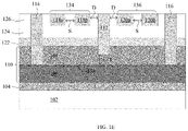
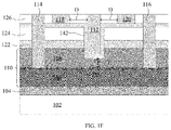
- an embodiment of a semiconductor device includes a substrate 102 , an active region 110 above the substrate 102 , and a source electrode 114 and a drain electrode 116 in contact with the active region 110 .
- the term “active region” may refer to a region that provides a pathway for the drifting of electrical charges between the source electrode 114 and the drain electrode 116 .
- a gate 112 is positioned above the active region 110 and laterally between the source electrode 114 and the drain electrode 116 .
- a first field plate 118 is positioned between the source electrode 114 and the gate 112
- a second field plate 120 is positioned between the drain electrode 116 and the gate 112 .
- the gate 112 is spaced apart laterally and substantially equidistant from the first field plate 118 and the second field plate 120 .
- the substrate 102 may include any semiconductor material, such as silicon, germanium, silicon germanium (SiGe), silicon carbide, and those consisting essentially of III-V compound semiconductors, such as gallium arsenide (GaAs), gallium nitride (GaN), II-VI compound semiconductors such as zinc selenide (ZnSe).
- the substrate 102 may include sapphire, spinel, zinc oxide (ZnO), aluminum nitride (AlN), or any other material capable of supporting the growth of Group III-nitride materials.
- the substrate 102 may be a bulk substrate as illustrated in the accompanying drawings.
- the substrate 102 may be a composite substrate structured to have multiple layers of the materials as described hereinbefore.
- the composite substrate may include, but not limited to, a silicon-on-ceramic substrate, Si/SiGe layered substrate, a silicon-on-insulator (SOI) substrate, a germanium-on-insulator (GOI) substrate, or a SiGe-on-insulator substrate.
- the gate 112 may be biased by a voltage to induce a conductive pathway within the active region to enable the drifting of electric charges between the source electrode 114 and the drain electrode 116 .
- the gate 112 may include a metallic material such as, but not limited to, tungsten, cobalt, nickel, copper, and aluminum.
- the conductance of the active region 110 may be controlled by the amount of voltage applied to the gate 112 .
- the active region 110 may have various structural configurations depending on the desired type of transistor.
- the active region 110 may include a heterostructure having multiple layers of materials.
- the active region 110 may be structured as a single doped layer to enable the drifting of charges across the source electrode 114 and the drain electrode 116 .
- the active region 110 may include a barrier layer 108 disposed upon a channel layer 106 .
- the channel layer 106 may include one or more sub-layers with a desired band gap. The sub-layers may be doped or undoped.
- the channel layer 106 may include a Group III-V compound, such as, but not limited to, GaAs, indium gallium arsenide (InGaAs), or GaN.
- the channel layer 106 may include the same material as the substrate 102 .
- the channel layer 106 may include a material different than the material in the substrate 102 .
- the barrier layer 108 has a band gap that is different from the band gap of the channel layer 106 .
- the barrier layer 108 may include one or more sub-layers and may be doped or undoped.
- the barrier layer 108 may include a Group III-V compound, such as, but not limited to, aluminum gallium arsenide (AlGaAs), or aluminum gallium nitride (AlGaN).
- a heterojunction may be formed at the interface between the barrier layer 108 and the channel layer 106 , resulting in the formation of a two-dimensional electron gas (2DEG) 138 in the channel layer 106 , which can provide the conductive pathway for the drifting of charges between the source electrode 114 and the drain electrode 116 .
- the barrier layer 108 and the channel layer 106 may be substantially undoped, and the 2DEG 138 may be induced by polarization mismatches between the barrier layer 108 and the channel layer 106 .
- the barrier layer 108 and the channel layer 106 may both be Group III-Nitride compounds, such as, but not limited to, GaN and AlGaN.
- the barrier layer 108 may be more highly doped than the channel layer 106 , which forms the 2DEG layer 138 .
- the gate 112 may be disposed above the channel layer 106 such that a lower surface of the gate 112 is spaced apart from an upper surface of the channel layer 106 by a distance T, in which the distance T may be between zero to a thickness of the barrier layer 108 .
- the gate 112 may be disposed upon the barrier layer 108 , in which the distance T equals the thickness of the barrier layer 108 .
- the barrier layer 108 may be partially recessed and a lower portion of the gate 112 may be disposed within the recessed portion of the barrier layer 108 .
- the gate 112 may be disposed upon the channel layer 106 through an opening defined in the barrier layer 108 such that the distance T equals zero.
- the source electrode 114 and the drain electrode 116 may contact the active region 110 in various configurations. As shown in FIG. 1A , the source electrode 114 and the drain electrode 116 may contact the channel layer 106 through the barrier layer 108 such that an electric current may flow between the source electrode 114 and the drain electrode 116 when the gate 112 is biased by a voltage. In other embodiments (not shown), the source electrode 114 and the drain electrode 116 may directly contact the barrier layer 108 , and form an electrical connection with the channel layer 106 through a diffusion-based thermal process.
- a transition layer 104 may be formed between the channel layer 106 and the substrate 102 .
- the transition layer 104 may serve to accommodate the lattice mismatch between the channel layer 106 and the substrate 102 , and thereby improving the “on” state and “off” state electrical characteristics of the device while accommodating bowing, warping, breakage or cracks of the substrate 102 .
- the transition layer 104 may be a superlattice structure with multiple sub-layers, or alternatively, be structured as a single layer.
- the transition layer 104 may include AlN, AlGaN, or GaN.
- Dielectric layers 124 , 126 may be disposed above the active region 110 .
- the dielectric layers 124 , 126 may be an inter-metal dielectric (IMD) layer or a “metallization level” that embeds various interconnect features.
- the dielectric layer 124 , 126 may include silicon nitride, silicon dioxide, tetraethyl orthosilicate (TEOS), or a material having a chemical composition of SiC x O y H z , wherein x, y, and z are in stoichiometric ratio.
- a capping layer 122 may be disposed between the barrier layer 108 and the dielectric layer 124 .
- the capping layer 122 may reduce the reverse current leakage from the active region 110 to the gate 112 , and increase the electric field strength in the barrier layer 108 when the device is in the “off” state.
- the capping layer 122 may include AlN, AlGaN, or GaN.
- the first field plate 118 and the second field plate 120 are arranged symmetrically around the gate 112 .
- the gate 112 may be equidistant and laterally spaced apart from the first field plate 118 and the second field plate 120 by a distance D.
- the distance D may vary depending on design requirements.
- the first field plate 118 and the second field plate 120 may be formed in the same dielectric layer (e.g., dielectric layer 126 ) and may have upper surfaces that are substantially coplanar with an upper surface of the gate 112 .
- the first field plate 118 and the second field plate 120 may include the same material as the gate 112 .
- first field plate 118 and the second field plate 120 may include the same material as the source electrode 114 and the drain electrode 116 .
- first field plate 118 and the second field plate 120 may include other metallic materials such as, but not limited to, gold (Au), titanium (Ti), nickel-gold (Ni—Au), or titanium-platinum-gold (Ti/Pt/Au).
- Unwanted capacitances may exist between the gate 112 and the drain electrode 116 (i.e., gate-to-drain capacitance) and between the gate 112 and the source electrode 114 (i.e., gate-to-source capacitance).
- the positioning of the first field plate 118 between the source electrode 114 and the gate 112 may reduce the gate-to-source capacitance while the positioning of the second field plate 120 between the drain electrode 116 and the gate 112 may reduce the gate-to-drain capacitance.
- the reduction of the gate-to-source and gate-to-drain capacitances by the respective first 118 and second 120 field plates and the arrangement of the gate 112 to be equidistant from the first field plate 118 and the second field plate 120 may achieve greater linearity and efficient power consumption of the device.
- the symmetric arrangement of the first field plate 118 and the second field plate 120 around the gate 112 may advantageously reduce undesirable harmonics generation and intermodulation distortion, as well as a reduced “off” state capacitance.
- a reduced “off” state capacitance may provide improved signal blocking capabilities when the device is in the “off” state.
- the device may be configured as a bi-directional switch.
- bi-directional switches may require a high breakdown voltage to sustain high voltages to the source/drain electrodes of the transistor.
- the symmetric arrangement of the first field plate 118 and the second field plate 120 around the gate 112 may reduce the surface electric field in the region between the gate 112 and the source electrode 114 , as well as the region between the gate 112 and the drain electrode 116 . Accordingly, the device can achieve a higher breakdown voltage between the source electrode 114 and the drain electrode 116 without experiencing large gate-to-source and gate-to-drain capacitances, and therefore enables the device to handle large power loads.
- the device can achieve shorter switching time between the “on” and “off” states.
- a shorter switching time can lead to lower power dissipation during the switching of the device, and the switching frequency can be further increased.
- the first field plate 118 may be laterally spaced apart from the source electrode 114
- the second field plate 120 may be laterally spaced apart from the drain electrode 116 .
- both of the first field plate 118 and the second field plate 120 may be conductively isolated (i.e., unbiased by a voltage and configured to float).
- the first field plate 118 and the second field plate 120 may be individually biased by a voltage.
- the voltage may be either a constant voltage or a variable voltage.
- the first field plate 118 and the second field plate 120 may be configured to be biased by the same voltage, or alternatively, the first field plate 118 and the second field plate 120 may be configured by different voltages.
- the first field plate 118 may be electrically coupled to the source electrode 114 and the second field plate 120 may be electrically coupled to the drain electrode 116 .
- Resistors may be used to couple the first field plate 118 with the source electrode 114 , as well as the second field plate 120 with the drain electrode 116 .
- FIG. 1B in which like reference numerals refer to like features in FIG. 1A , another embodiment of a semiconductor device is shown.
- the embodiment shown in FIG. 1B is similar to the embodiment shown in FIG. 1A except that in FIG. 1B , the gate 112 is disposed on the capping layer 122 .
- the capping layer 122 may be configured as an electrical insulator for the gate 112 to modulate the conductance of the active region 110 .
- the capping layer 122 may also reduce the reverse current leakage from the active region 110 to the gate 112 , and increase the electric field strength in the barrier layer 108 when the device is in the “off” state.
- the gate 112 may have field plate extensions 113 a , 113 b that extend laterally from the gate 112 towards the source 114 and drain 116 electrodes.
- the field plate extensions 113 a , 113 b may have upper surfaces that are substantially coplanar with the upper surfaces of the first field plate 118 and the second field plate 120 .
- the field plate extensions 113 a , 113 b may be integrally formed with the gate 112 , and may be referred to as a “T-shaped” gate.
- the inclusion of the field plate extensions 113 a , 113 b may increase the breakdown voltage of the device.
- the field plate extensions 113 a , 113 b are structured symmetrically around the gate 112 .
- the field plate extensions 113 a , 113 b may have identical lengths of extension from lateral sides of the gate 112 .
- the gate 112 and its field plate extensions 113 a , 113 b are positioned equidistant from the source electrode 114 and the drain electrode 116 .
- the field plate extensions 113 a , 113 b may be laterally spaced apart from the source electrode 114 and the drain electrode 116 , respectively, by a distance D.
- Additional field plates may be formed above the first field plate 118 and the second field plate 120 .
- a third field plate 130 and a fourth field plate 132 may be formed within a dielectric layer 128 .
- the dielectric layer 128 may be an additional inter-metal dielectric (IMD) layer or a “metallization level” that is deposited vertically above the dielectric layer 126 .
- IMD inter-metal dielectric
- the third field plate 130 and the fourth field plate 132 may be positioned symmetrically around the gate 112 (i.e., being equidistant from the gate 112 ).
- Positioning additional field plates above the first field plate 118 and the second field plate 120 may offer an advantage of further reducing the capacitance and the surface electric field in the regions between the gate 112 and the source electrode 114 , and the gate 112 and the drain electrode 116 , which may lead to further increases in linearity and more efficient power consumption.
- FIG. 1E in which like reference numerals refer to like features in FIG. 1A , another embodiment of a semiconductor device is shown.
- the embodiment in FIG. 1E may include a first set of field plates 134 and a second set of field plates 136 .
- the first set of field plates 134 may be positioned between the source electrode 114 and the gate 112
- the second set of field plates 136 may be positioned between the drain electrode 116 and the gate 112 .
- the first set of field plates 134 and the second set of field plates 136 may be symmetrically arranged around the gate 112 .
- the gate 112 may be equidistant and laterally spaced apart from the first set of field plates 134 and the second set of field plates 136 by a distance D.
- the first set of field plates 134 and the second set of field plates 136 may include multiple field plates.
- the field plates 118 a , 118 b in the first set 134 and the field plates 120 a , 120 b in the second set 136 may have upper surfaces that are substantially coplanar with an upper surface of the gate 112 .
- the number of field plates in the first set 134 may be identical to the number of field plates in the second set 136 .
- Each field plate 118 a , 118 b in the first set 134 and each field plate 120 a , 120 b in the second set 136 may be spaced apart from one another by a spacing S.
- the spacing between each field plate in the first set 134 may be identical to the spacing between each field plate in the second set 136 .
- the symmetrical arrangement of multiple field plates around the gate 112 may further reduce the capacitance and the surface electric field in the regions between the gate 112 and the source electrode 114 , and the gate 112 and the drain electrode 116 , which may lead to further increases in linearity and more efficient power consumption.
- FIG. 1E has a “T-shaped” gate as described in FIG. 1B .
- FIG. IF illustrates another embodiment of the semiconductor device.
- the embodiment shown in FIG. IF is similar to the embodiment shown in FIG. 1A except that in FIG. 1F , the gate 112 may be configured over a gate dielectric layer 142 .
- the gate 112 and the gate dielectric layer 142 may be disposed above the channel layer 106 such that the gate dielectric layer 142 is spaced apart from an upper surface of the channel layer 106 by a distance T, in which the distance T may be between zero to a thickness of the barrier layer 108 .
- the gate dielectric layer 142 may be disposed upon the upper surface of the channel layer 106 such that the distance T is zero.
- the gate dielectric layer 142 may be disposed upon an upper surface of the barrier layer 108 such that the distance T is equal to the thickness of the barrier layer 108 .
- the gate dielectric layer 142 may extend over the dielectric layer 124 .
- the first field plate 118 and the second field plate 120 may be disposed on the gate dielectric layer 142 .
- the gate dielectric layer 142 may include silicon dioxide (SiO 2 ), a high-k dielectric material, silicon oxynitride, other suitable materials, or combinations thereof.
- the high-k dielectric material may have a dielectric constant (i.e., K value) that is greater than 5, preferably between 20 to 30.
- Examples of the high-k dielectric material may include, but not limited to, metal oxides, metal nitrides, metal silicates, transition metal oxides, transition metal nitrides, transition metal silicates, oxynitrides of metals, metal aluminates, hafnium oxide (HfO 2 ), zirconium oxide (ZrO 2 ), lanthanum oxide (La 2 O 3 ), aluminum oxide (Al 2 O 3 ), titanium oxide (TiO 2 ), strontium titanium oxide (SrTiO 3 ), lanthanum aluminum oxide (LaAlO3), yttrium oxide (Y 2 O 3 ), zirconium silicate, zirconium aluminate, or combinations thereof.
- FIG. 2 through FIG. 5 show a set of steps that may be used to create the semiconductor devices as provided for in embodiments of the present disclosure.
- deposition techniques refer to the process of applying a material over another material (or the substrate).
- exemplary techniques for deposition include, but not limited to, spin-on coating, sputtering, chemical vapor deposition (CVD), physical vapor deposition (PVD), molecular beam deposition (MBD), pulsed laser deposition (PLD), liquid source misted chemical deposition (LSMCD), atomic layer deposition (ALD).
- patterning techniques includes deposition of material or photoresist, patterning, exposure, development, etching, cleaning, and/or removal of the material or photoresist as required in forming a described pattern, structure or opening.
- techniques for patterning include, but not limited to, wet etch lithographic processes, dry etch lithographic processes or direct patterning processes. Such techniques may use mask sets and mask layers.
- FIG. 2 a device structure for use in fabricating the semiconductor devices of the present disclosure is shown.
- an active region 110 above a substrate 102 .
- a capping layer 122 may be provided upon the active region 110 .
- the active region 110 may include a barrier layer 108 disposed on a channel layer 106 .
- the capping layer 122 may be disposed upon the barrier layer 108 .
- a first dielectric layer 124 may be deposited on the capping layer 122 using deposition techniques as described herein.
- the first dielectric layer 124 and the capping layer 122 may be patterned to define an opening 148 using patterning techniques as described herein.
- an etching process to form the opening 148 may be stopped such that a lower surface of the opening 148 is spaced apart from an upper surface of the channel layer 106 by a distance T, in which the distance T may be between zero to a thickness of the barrier layer 108 .
- the opening 148 may expose the barrier layer 108 .
- the opening 148 may expose the channel layer 106 by etching through the barrier layer 108 .
- FIG. 3 illustrates the formation of a metal layer 150 above the active region 110 .
- the metal layer 150 may be deposited on the first dielectric layer 124 using the deposition techniques described herein.
- the deposited metal layer 150 also fills the opening 148 .
- a gate dielectric layer may be deposited in the opening 148 and on the first dielectric layer 124 before depositing the metal layer 150 .
- FIG. 4 illustrates the formation a gate 112 , a first field plate 118 , and a second field plate 120 .
- the metal layer 150 may be patterned using the patterning techniques described herein to form the gate 112 , the first field plate 118 and the second field plate 120 .
- the gate 112 may form a Schottky contact with the active region 110 .
- the first field plate 118 and the second field plate 120 may have upper surfaces that are substantially coplanar with an upper surface of the gate 112 .
- the patterning of the metal layer 150 also ensures that the first field plate 118 and the second field plate 120 are spaced apart from the gate 112 by a distance D.
- the metal layer 150 may also be patterned to form the “T-shaped” gate, as described in FIG. 1B . Additionally, the patterning of the metal layer 150 may also form a first set of field plates and a second set of field plates, as described in FIG. 1D .
- the fabrication of the first field plate 118 and the second field plate 120 does not require an additional mask (or reticle) and/or additional processes, such as deposition and etching of materials, which reduces fabrication costs.
- the first field plate 118 and the second field plate 120 can be formed using the same mask that is being used to form the gate 112
- a second dielectric layer 126 may be deposited on the first dielectric layer 124 using the deposition techniques described herein.
- the deposited dielectric layer 126 may fill the distance D between the first field plate 118 and the gate 112 , and between the second field plate 120 and the gate 112 .
- source/drain openings 152 are formed by etching through the dielectric layers 124 , 126 , the capping layer 122 , and the barrier layer 108 .
- Source and drain electrodes are subsequently formed by filling the source/drain openings 152 with a metallic material such as, but not limited to, tungsten, cobalt, nickel, copper, and aluminum. In some embodiments, the source and drain electrodes may form ohmic contacts with the active region 110 .
- the semiconductor devices of the present disclosure may include transistors suitable for use in microwave or millimeter-wave power amplification applications as well as radio frequency applications.
- the semiconductor devices of the present disclosure may also be capable of handling frequencies in the magnitude of 1-100 gigahertz, as well as voltages in the magnitude of 1.2-600 volts.
- transistors may include, but not limited to, a high electron mobility transistor (HEMT) (e.g., an aluminum gallium nitride (AlGaN)/gallium nitride (GaN) HEMT), a pseudomorphic HEMT (PHEMT) (e.g., a gallium arsenide (GaAs) PHEMT), a metamorphic HEMT (mHEMT) (e.g., a GaAs mHEMT), a laterally diffused metal oxide semiconductor transistor (LDMOS), a metal oxide semiconductor field effect transistor (MOSFET), a metal insulator semiconductor high electron mobility transistor (MISHEMT), or a metal epitaxial semiconductor field effect transistor (MESFET).
- HEMT high electron mobility transistor
- AlGaN aluminum gallium nitride
- GaN gallium nitride
- PHEMT pseudomorphic HEMT
- mHEMT metamorphic HEMT
- LDMOS laterally diffused metal oxide
- the disclosed semiconductor devices and methods of forming the same may be employed in manufacturing a variety of different integrated circuit products, including, but not limited to, high power electronic devices, communication devices, high electron mobility transistors, etc.
Landscapes
- Junction Field-Effect Transistors (AREA)
- Insulated Gate Type Field-Effect Transistor (AREA)
- Engineering & Computer Science (AREA)
- Manufacturing & Machinery (AREA)
Abstract
Description
Claims (20)
Priority Applications (3)
| Application Number | Priority Date | Filing Date | Title |
|---|---|---|---|
| US16/942,734 US11316019B2 (en) | 2020-07-29 | 2020-07-29 | Symmetric arrangement of field plates in semiconductor devices |
| CN202110736273.2A CN114068682B (en) | 2020-07-29 | 2021-06-30 | Symmetrical arrangement of field plates in semiconductor devices |
| US17/650,854 US11616127B2 (en) | 2020-07-29 | 2022-02-13 | Symmetric arrangement of field plates in semiconductor devices |
Applications Claiming Priority (1)
| Application Number | Priority Date | Filing Date | Title |
|---|---|---|---|
| US16/942,734 US11316019B2 (en) | 2020-07-29 | 2020-07-29 | Symmetric arrangement of field plates in semiconductor devices |
Related Child Applications (1)
| Application Number | Title | Priority Date | Filing Date |
|---|---|---|---|
| US17/650,854 Division US11616127B2 (en) | 2020-07-29 | 2022-02-13 | Symmetric arrangement of field plates in semiconductor devices |
Publications (2)
| Publication Number | Publication Date |
|---|---|
| US20220037482A1 US20220037482A1 (en) | 2022-02-03 |
| US11316019B2 true US11316019B2 (en) | 2022-04-26 |
Family
ID=80003427
Family Applications (2)
| Application Number | Title | Priority Date | Filing Date |
|---|---|---|---|
| US16/942,734 Active 2040-08-06 US11316019B2 (en) | 2020-07-29 | 2020-07-29 | Symmetric arrangement of field plates in semiconductor devices |
| US17/650,854 Active US11616127B2 (en) | 2020-07-29 | 2022-02-13 | Symmetric arrangement of field plates in semiconductor devices |
Family Applications After (1)
| Application Number | Title | Priority Date | Filing Date |
|---|---|---|---|
| US17/650,854 Active US11616127B2 (en) | 2020-07-29 | 2022-02-13 | Symmetric arrangement of field plates in semiconductor devices |
Country Status (2)
| Country | Link |
|---|---|
| US (2) | US11316019B2 (en) |
| CN (1) | CN114068682B (en) |
Families Citing this family (4)
| Publication number | Priority date | Publication date | Assignee | Title |
|---|---|---|---|---|
| US20240120825A1 (en) * | 2022-10-04 | 2024-04-11 | Wisconsin Alumni Research Foundation | High-Efficiency Drive Circuit And Bidirectional FET |
| CN117080247A (en) * | 2023-10-11 | 2023-11-17 | 荣耀终端有限公司 | Gallium nitride heterojunction field effect transistor, manufacturing method and electronic device |
| US20250142860A1 (en) * | 2023-10-30 | 2025-05-01 | Globalfoundries U.S. Inc. | High electron mobility transistor with regrown barrier structure |
| US20250248097A1 (en) * | 2024-01-30 | 2025-07-31 | Globalfoundries U.S. Inc. | Device with outer conductive spacer |
Citations (10)
| Publication number | Priority date | Publication date | Assignee | Title |
|---|---|---|---|---|
| US7812369B2 (en) | 2003-09-09 | 2010-10-12 | The Regents Of The University Of California | Fabrication of single or multiple gate field plates |
| US7875907B2 (en) | 2007-09-12 | 2011-01-25 | Transphorm Inc. | III-nitride bidirectional switches |
| US8754496B2 (en) | 2009-04-14 | 2014-06-17 | Triquint Semiconductor, Inc. | Field effect transistor having a plurality of field plates |
| US8866191B2 (en) | 2007-02-22 | 2014-10-21 | Forschungsverbund Berlin E.V. | HEMT semiconductor component with field plates |
| US20140361342A1 (en) | 2013-06-09 | 2014-12-11 | Cree, Inc. | Recessed field plate transistor structures |
| US9142659B2 (en) | 2011-03-04 | 2015-09-22 | Transphorm Inc. | Electrode configurations for semiconductor devices |
| WO2019066878A1 (en) * | 2017-09-28 | 2019-04-04 | Intel Corporation | Gallium nitride transistors with source and drain field plates and their methods of fabrication |
| US20190207022A1 (en) * | 2017-12-27 | 2019-07-04 | Rohm Co., Ltd. | Semiconductor device and manufacturing method thereof |
| CN111403480A (en) * | 2020-03-21 | 2020-07-10 | 中山市华南理工大学现代产业技术研究院 | High-voltage AlGaN/GaN HEMT device and preparation method thereof |
| US20210328029A1 (en) * | 2020-04-17 | 2021-10-21 | Innoscience (Zhuhai) Technology Co., Ltd. | Semiconductor device and manufacturing method thereof |
Family Cites Families (9)
| Publication number | Priority date | Publication date | Assignee | Title |
|---|---|---|---|---|
| US7573078B2 (en) * | 2004-05-11 | 2009-08-11 | Cree, Inc. | Wide bandgap transistors with multiple field plates |
| US11791385B2 (en) * | 2005-03-11 | 2023-10-17 | Wolfspeed, Inc. | Wide bandgap transistors with gate-source field plates |
| JP2007180143A (en) * | 2005-12-27 | 2007-07-12 | Toshiba Corp | Nitride semiconductor device |
| US8212290B2 (en) * | 2007-03-23 | 2012-07-03 | Cree, Inc. | High temperature performance capable gallium nitride transistor |
| US8791503B2 (en) * | 2007-09-18 | 2014-07-29 | International Rectifier Corporation | III-nitride semiconductor device with reduced electric field between gate and drain and process for its manufacture |
| CN105322005B (en) * | 2015-04-17 | 2018-07-06 | 苏州捷芯威半导体有限公司 | A kind of semiconductor devices and preparation method thereof |
| US9911817B2 (en) * | 2015-07-17 | 2018-03-06 | Cambridge Electronics, Inc. | Field-plate structures for semiconductor devices |
| US11398546B2 (en) * | 2019-08-06 | 2022-07-26 | Vanguard International Semiconductor Corporation | Semiconductor devices and methods for fabricating the same |
| CN114747018A (en) * | 2019-12-03 | 2022-07-12 | 剑桥电子有限公司 | III-nitride transistor with improved drain access region |
-
2020
- 2020-07-29 US US16/942,734 patent/US11316019B2/en active Active
-
2021
- 2021-06-30 CN CN202110736273.2A patent/CN114068682B/en active Active
-
2022
- 2022-02-13 US US17/650,854 patent/US11616127B2/en active Active
Patent Citations (10)
| Publication number | Priority date | Publication date | Assignee | Title |
|---|---|---|---|---|
| US7812369B2 (en) | 2003-09-09 | 2010-10-12 | The Regents Of The University Of California | Fabrication of single or multiple gate field plates |
| US8866191B2 (en) | 2007-02-22 | 2014-10-21 | Forschungsverbund Berlin E.V. | HEMT semiconductor component with field plates |
| US7875907B2 (en) | 2007-09-12 | 2011-01-25 | Transphorm Inc. | III-nitride bidirectional switches |
| US8754496B2 (en) | 2009-04-14 | 2014-06-17 | Triquint Semiconductor, Inc. | Field effect transistor having a plurality of field plates |
| US9142659B2 (en) | 2011-03-04 | 2015-09-22 | Transphorm Inc. | Electrode configurations for semiconductor devices |
| US20140361342A1 (en) | 2013-06-09 | 2014-12-11 | Cree, Inc. | Recessed field plate transistor structures |
| WO2019066878A1 (en) * | 2017-09-28 | 2019-04-04 | Intel Corporation | Gallium nitride transistors with source and drain field plates and their methods of fabrication |
| US20190207022A1 (en) * | 2017-12-27 | 2019-07-04 | Rohm Co., Ltd. | Semiconductor device and manufacturing method thereof |
| CN111403480A (en) * | 2020-03-21 | 2020-07-10 | 中山市华南理工大学现代产业技术研究院 | High-voltage AlGaN/GaN HEMT device and preparation method thereof |
| US20210328029A1 (en) * | 2020-04-17 | 2021-10-21 | Innoscience (Zhuhai) Technology Co., Ltd. | Semiconductor device and manufacturing method thereof |
Also Published As
| Publication number | Publication date |
|---|---|
| US20220165853A1 (en) | 2022-05-26 |
| US20220037482A1 (en) | 2022-02-03 |
| US11616127B2 (en) | 2023-03-28 |
| CN114068682A (en) | 2022-02-18 |
| CN114068682B (en) | 2024-08-16 |
Similar Documents
| Publication | Publication Date | Title |
|---|---|---|
| US11616127B2 (en) | Symmetric arrangement of field plates in semiconductor devices | |
| JP6124511B2 (en) | Wide band gap transistor including gate-source field plate | |
| KR101108300B1 (en) | Wide bandgap transistor devices with field plates | |
| EP3522231B1 (en) | Multi-gate transistor | |
| US11695052B2 (en) | III-Nitride transistor with a cap layer for RF operation | |
| KR20220020901A (en) | High Electron Mobility Transistors and Power Amplifiers Including Transistors with Improved Performance and Reliability | |
| WO2007126541A1 (en) | High efficiency and/or high power density wide bandgap transistors | |
| TW201405823A (en) | a three-group nitride transistor using a re-growth structure | |
| KR20240008373A (en) | Methods for manufacturing high electron mobility transistors with improved performance | |
| US20110204380A1 (en) | Nitride-based fet | |
| US9349848B2 (en) | Gateless switch with capacitively-coupled contacts | |
| US12266713B2 (en) | Transistor with dielectric spacers and method of fabrication therefor | |
| US20230043810A1 (en) | Iii-nitride transistor with electrically connected p-type layer in access region | |
| US20220165873A1 (en) | Hemt and method of fabricating the same | |
| TWI509795B (en) | Wide band gap transistor device with field plate | |
| US12513981B2 (en) | Semiconductor device | |
| CN222547914U (en) | Semiconductor devices and HEMT devices | |
| US20250248097A1 (en) | Device with outer conductive spacer | |
| US12369380B2 (en) | Transistor with dielectric spacers and field plate and method of fabrication therefor | |
| US20240304711A1 (en) | Hemt device having a reduced on-resistance and manufacturing process thereof | |
| US20240304713A1 (en) | Hemt device having a reduced gate leakage and manufacturing process thereof | |
| Panda et al. | Metal oxide semiconductor high electron mobility transistors | |
| Agrawal et al. | TERM PAPER (EE 311) AlGaN/GaN HEMT: AN OVERVIEW OF DEVICE OPERATION, ITS ADVANTAGES AND LIMITATIONS |
Legal Events
| Date | Code | Title | Description |
|---|---|---|---|
| AS | Assignment |
Owner name: GLOBALFOUNDRIES INC., CAYMAN ISLANDS Free format text: ASSIGNMENT OF ASSIGNORS INTEREST;ASSIGNORS:KANTAROVSKY, JOHNATAN AVRAHAM;KRISHNASAMY, RAJENDRAN;ADUSUMILLI, SIVA P.;AND OTHERS;REEL/FRAME:053347/0857 Effective date: 20200729 |
|
| FEPP | Fee payment procedure |
Free format text: ENTITY STATUS SET TO UNDISCOUNTED (ORIGINAL EVENT CODE: BIG.); ENTITY STATUS OF PATENT OWNER: LARGE ENTITY |
|
| AS | Assignment |
Owner name: GLOBALFOUNDRIES U.S. INC., CALIFORNIA Free format text: ASSIGNMENT OF ASSIGNORS INTEREST;ASSIGNOR:GLOBALFOUNDRIES INC.;REEL/FRAME:054633/0001 Effective date: 20201022 |
|
| AS | Assignment |
Owner name: GLOBALFOUNDRIES U.S. INC., NEW YORK Free format text: RELEASE BY SECURED PARTY;ASSIGNOR:WILMINGTON TRUST, NATIONAL ASSOCIATION;REEL/FRAME:056987/0001 Effective date: 20201117 Owner name: GLOBALFOUNDRIES U.S. INC., NEW YORK Free format text: RELEASE OF SECURITY INTEREST;ASSIGNOR:WILMINGTON TRUST, NATIONAL ASSOCIATION;REEL/FRAME:056987/0001 Effective date: 20201117 |
|
| STPP | Information on status: patent application and granting procedure in general |
Free format text: NOTICE OF ALLOWANCE MAILED -- APPLICATION RECEIVED IN OFFICE OF PUBLICATIONS |
|
| STPP | Information on status: patent application and granting procedure in general |
Free format text: PUBLICATIONS -- ISSUE FEE PAYMENT VERIFIED |
|
| STCF | Information on status: patent grant |
Free format text: PATENTED CASE |
|
| MAFP | Maintenance fee payment |
Free format text: PAYMENT OF MAINTENANCE FEE, 4TH YEAR, LARGE ENTITY (ORIGINAL EVENT CODE: M1551); ENTITY STATUS OF PATENT OWNER: LARGE ENTITY Year of fee payment: 4 |