[go: up one dir, main page]

TW202036942A - Manufacturing method of micro fluid actuator module - Google Patents

Manufacturing method of micro fluid actuator module Download PDF

Info

Publication number
TW202036942A
TW202036942A TW108111391A TW108111391A TW202036942A TW 202036942 A TW202036942 A TW 202036942A TW 108111391 A TW108111391 A TW 108111391A TW 108111391 A TW108111391 A TW 108111391A TW 202036942 A TW202036942 A TW 202036942A
Authority
TW
Taiwan
Prior art keywords
layer
substrate
actuator module
manufacturing
microfluidic actuator
Prior art date
Application number
TW108111391A
Other languages
Chinese (zh)
Other versions
TWI683462B (en
Inventor
莫皓然
余榮侯
張正明
戴賢忠
廖文雄
黃啟峰
韓永隆
陳宣愷
Original Assignee
研能科技股份有限公司
Priority date (The priority date is an assumption and is not a legal conclusion. Google has not performed a legal analysis and makes no representation as to the accuracy of the date listed.)
Filing date
Publication date
Application filed by 研能科技股份有限公司 filed Critical 研能科技股份有限公司
Priority to TW108111391A priority Critical patent/TWI683462B/en
Application granted granted Critical
Publication of TWI683462B publication Critical patent/TWI683462B/en
Publication of TW202036942A publication Critical patent/TW202036942A/en

Links

Images

Landscapes

  • Micromachines (AREA)

Abstract

A manufacturing method of a micro fluid actuator module is disclosed and comprises following steps of (1) providing a first substrate to deposit and etch a first protection layer, (2) rolling and developing a first photoresist layer on the first protection layer, (3) providing an auxiliary substrate to roll and etch a film layer and a valve layer on the auxiliary substrate, (4) flipping and positioning the valve layer to be jointed with the first photoresist layer, (5) providing a second substrate, (6) rolling and developing a second photoresist layer on the second substrate, (7) flip-chipping and hot pressing the second photoresist layer on the valve layer, (8) screen printing a conductive adhesive layer on the second substrate, (9) pasting a piezoelectric layer on the conductive adhesive layer, and (10) welding an electrode layer on the piezoelectric layer and the second substrate.

Description

微流體致動器模組之製造方法Manufacturing method of microfluidic actuator module

本案關於一種微流體致動器模組之製造方法,尤指一種使用微機電面型及體型加工製程之微流體致動器模組之製造方法。This case relates to a method of manufacturing a microfluidic actuator module, especially a method of manufacturing a microfluidic actuator module using a microelectromechanical surface and body processing process.

目前於各領域中無論是醫藥、電腦科技、列印、能源等工業,產品均朝精緻化及微小化方向發展,其中微幫浦、噴霧器、噴墨頭、工業列印裝置等產品所包含之流體致動器為其關鍵技術。At present, in various fields, whether it is medicine, computer technology, printing, energy and other industries, products are developing in the direction of refinement and miniaturization. Among them, products such as micro pumps, sprayers, inkjet heads, and industrial printing devices include Fluid actuator is its key technology.

隨著科技的日新月異,流體輸送結構的應用上亦愈來愈多元化,舉凡工業應用、生醫應用、醫療保健、電子散熱……等,甚至近來熱門的穿戴式裝置皆可見它的踨影,可見傳統的流體致動器已漸漸有朝向裝置微小化、流量極大化的趨勢。With the rapid development of science and technology, the application of fluid transport structure is becoming more and more diversified. For example, industrial applications, biomedical applications, medical care, electronic heat dissipation, etc., even the recently popular wearable devices can see its shadow. It can be seen that the traditional fluid actuators have gradually tended towards miniaturization of devices and maximization of flow rate.

現有技術中已發展多種微機電製程製出之微流體致動器,然而,藉創新結構增進流體傳輸之功效,仍為發展之重要內容。A variety of microfluidic actuators produced by microelectromechanical processes have been developed in the prior art. However, it is still an important development content to improve the efficiency of fluid transmission through innovative structures.

本案之主要目的係提供一種微流體致動器模組之製造方法,使用微機電面型及體型加工製程,並輔以精密封裝技術一體成型製作而成。The main purpose of this case is to provide a method for manufacturing a microfluidic actuator module, which uses micro-electromechanical surface and body processing processes, and is manufactured by integrated molding with precision packaging technology.

本案之一廣義實施態樣為一種微流體致動器模組之製造方法,包含以下步驟:1.提供一第一基板沉積及蝕刻一第一保護層;2.該第一保護層滾壓及顯影一第一光阻層;3.提供一輔助基板滾壓及蝕刻一薄膜膠層以及一閥層;4.該閥層翻轉對位以及接合於該第一光阻層上;5.提供一第二基板;6.該第二基板滾壓及顯影一第二光阻層;7.該第二光阻層覆晶以及熱壓接合於該閥層;8.該第二基板網印一導電膠層;9.該導電膠層黏貼一壓電層;以及10.該壓電層以及該第二基板焊接一電極層。第一基板具有一第一表面及一第二表面,係先透過一氮化材料沉積製程形成於第一基板之第一表面上以形成第一保護層,再透過蝕刻製程形成複數個出口開口、複數個流體出口以及複數個噴口。出口開口分別透過流體出口與噴口相連通。透過一光阻材料滾壓製程形成於第一保護層上以形成第一光阻層,再透過顯影製程形成一連通流道、複數個入口流道、複數個閥座以及複數個腔體開口。透過一薄膜材料滾壓製程形成於輔助基板上以形成薄膜膠層,再透過一聚合材料滾壓製程形成於薄膜膠層上以形成閥層,最後透過蝕刻製程形成複數個出口閥、複數個入口閥以及一第一流道開口。透過翻轉對位以及接合製程將閥層接合於第一光阻層,再透過浸泡移除輔助基板。閥層之第一流道開口與第一光阻層之連通流道相連通。透過蝕刻製程形成複數個振動開口,並定義複數個振動區。振動區分別與振動開口的位置相對應。透過光阻材料滾壓製程形成於第二基板上以形成第二光阻層,再透過顯影製程形成複數個腔體孔洞以及一第二流道開口。透過覆晶以及熱壓製程將第二光阻層接合於閥層。第二光阻層之腔體孔洞分別與第二基板之振動開口以及第一光阻層之腔體開口相連通,藉以形成複數個振動腔室。第二光阻層之第二流道開口透過閥層之第一流道開口與第一光阻層之連通流道相連通。透過一導電膠材網印製程形成於第二基板上以形成導電膠層。透過一壓電材料黏貼製程形成於導電膠層上以形成壓電層,再透過切割製程定義複數個致動區。透過一電極材料焊接製程形成於壓電層以及第二基板上以形成電極層。電極層具有複數個上電極區以及複數個下電極區。A broad implementation aspect of this case is a method for manufacturing a microfluidic actuator module, which includes the following steps: 1. Providing a first substrate to deposit and etching a first protective layer; 2. Rolling the first protective layer and Develop a first photoresist layer; 3. Provide an auxiliary substrate for rolling and etching a thin film adhesive layer and a valve layer; 4. The valve layer is flipped and aligned and bonded to the first photoresist layer; 5. Provide a The second substrate; 6. The second substrate rolls and develops a second photoresist layer; 7. The second photoresist layer is flip-chip and thermocompression bonded to the valve layer; 8. The second substrate is screen printed with a conductive Adhesive layer; 9. The conductive adhesive layer is pasted with a piezoelectric layer; and 10. The piezoelectric layer and the second substrate are welded to an electrode layer. The first substrate has a first surface and a second surface. It is formed on the first surface of the first substrate through a nitride material deposition process to form a first protective layer, and then a plurality of exit openings are formed through an etching process, Multiple fluid outlets and multiple nozzles. The outlet openings are respectively communicated with the nozzle through the fluid outlet. A photoresist material rolling process is formed on the first protective layer to form the first photoresist layer, and then a communication flow channel, a plurality of inlet flow channels, a plurality of valve seats and a plurality of cavity openings are formed by a development process. A thin film material rolling process is formed on the auxiliary substrate to form a thin film adhesive layer, and then a polymer material rolling process is formed on the thin film adhesive layer to form a valve layer, and finally a plurality of outlet valves and a plurality of inlets are formed through an etching process The valve and a first flow passage opening. The valve layer is bonded to the first photoresist layer through the reverse alignment and bonding process, and then the auxiliary substrate is removed by immersion. The first flow channel opening of the valve layer is communicated with the communicating flow channel of the first photoresist layer. A plurality of vibration openings are formed through an etching process, and a plurality of vibration regions are defined. The vibration area corresponds to the position of the vibration opening respectively. The photoresist material rolling process is formed on the second substrate to form the second photoresist layer, and then a plurality of cavity holes and a second flow channel opening are formed through the development process. The second photoresist layer is bonded to the valve layer through flip chip and hot pressing process. The cavity holes of the second photoresist layer are respectively communicated with the vibration openings of the second substrate and the cavity openings of the first photoresist layer, thereby forming a plurality of vibration chambers. The second flow channel opening of the second photoresist layer communicates with the communication channel of the first photoresist layer through the first flow channel opening of the valve layer. A conductive adhesive material screen printing process is formed on the second substrate to form a conductive adhesive layer. A piezoelectric material pasting process is formed on the conductive adhesive layer to form a piezoelectric layer, and then a plurality of actuation regions are defined by a cutting process. An electrode material welding process is formed on the piezoelectric layer and the second substrate to form the electrode layer. The electrode layer has a plurality of upper electrode regions and a plurality of lower electrode regions.

體現本案特徵與優點的實施例將在後段的說明中詳細敘述。應理解的是本案能夠在不同的態樣上具有各種的變化,其皆不脫離本案的範圍,且其中的說明及圖示在本質上當作說明之用,而非用以限制本案。The embodiments embodying the features and advantages of this case will be described in detail in the later description. It should be understood that this case can have various changes in different aspects, all of which do not depart from the scope of the case, and the descriptions and illustrations therein are essentially for illustrative purposes, rather than limiting the case.

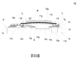
本案之微流體致動器用於輸送流體,請參閱第1圖以及第4圖,於本案實施例中,微流體致動器模組100包含複數個微流體致動器10,且由一第一基板1a、一第一保護層1b、一第一光阻層1c、一輔助基板1d(如第2H圖到第2J圖)、一薄膜膠層1e(如第2H圖到第2J圖)、一閥層1f、一第二基板1g、一第二光阻層1h、一導電膠層1i、一壓電層1j以及一電極層1k組成,其製造方法如下步驟說明,並且其製程將以單個微流體致動器10做為說明。The microfluidic actuator in this case is used to transport fluid. Please refer to Figures 1 and 4. In the embodiment of this case, the microfluidic actuator module 100 includes a plurality of microfluidic actuators 10, and a first Substrate 1a, a first protective layer 1b, a first photoresist layer 1c, an auxiliary substrate 1d (as shown in Figure 2H to Figure 2J), a thin film adhesive layer 1e (as shown in Figure 2H to Figure 2J), a The valve layer 1f, a second substrate 1g, a second photoresist layer 1h, a conductive adhesive layer 1i, a piezoelectric layer 1j and an electrode layer 1k are composed. The manufacturing method is described in the following steps, and the manufacturing process will be a single micro The fluid actuator 10 is for illustration.

請參閱第2圖至第3E圖,如步驟S1所示,提供一第一基板沉積、蝕刻一第一保護層。於本案實施例中,第一基板1a具有一第一表面11a以及一相對於第一表面11a之第二表面12a,係先透過一氮化材料沉積製程形成於第一基板1a之第一表面11a之上以形成第一保護層1b,再透過蝕刻製程形成第一保護層1b之一出口開口11b以及第一基板1a之一流體出口14a,再透過一研磨製程使第一基板1a薄化,最後透過蝕刻製程形成第一基板1a之一噴口15a。其中,第一保護層1b之出口開口11b透過第一基板1a之流體出口14a與噴口15a相連通。於本案實施例中,第一基板1a為一矽基材,但不以此為限。於本案實施例中,氮化材料為一氮化矽材料,但不以此為限。於本案實施例中,第一基板1a透過一深蝕刻製程製出流體出口14a,但不以此為限。於本案實施例中,第一基板1a透過一乾式蝕刻製程製出噴口15a,但不以此為限。於本案實施例中,第一保護層1b之沉積製程為一化學氣相沉積製程(CVD),但不以此為限。於本案實施例中,第一保護層1b之蝕刻製程可為一濕式蝕刻製程、一乾式蝕刻製程或兩者之組合,但不以此為限。於本案實施例中,第一基板1a包含一IC線路13a,設置於第一基板1a上。Referring to FIGS. 2 to 3E, as shown in step S1, a first substrate is provided to deposit and etch a first protective layer. In this embodiment, the first substrate 1a has a first surface 11a and a second surface 12a opposite to the first surface 11a, which is formed on the first surface 11a of the first substrate 1a through a nitride material deposition process. A first protective layer 1b is formed on it, an outlet opening 11b of the first protective layer 1b and a fluid outlet 14a of the first substrate 1a are formed through an etching process, and then the first substrate 1a is thinned through a grinding process, and finally A nozzle 15a of the first substrate 1a is formed through an etching process. The outlet opening 11b of the first protective layer 1b communicates with the nozzle 15a through the fluid outlet 14a of the first substrate 1a. In the embodiment of this case, the first substrate 1a is a silicon substrate, but it is not limited to this. In the embodiment of this case, the nitride material is a silicon nitride material, but it is not limited to this. In the embodiment of this case, the fluid outlet 14a is formed on the first substrate 1a through a deep etching process, but it is not limited to this. In the embodiment of this case, the first substrate 1a is formed with the nozzle 15a through a dry etching process, but it is not limited to this. In the embodiment of this case, the deposition process of the first protection layer 1b is a chemical vapor deposition process (CVD), but it is not limited thereto. In the embodiment of this case, the etching process of the first protective layer 1b can be a wet etching process, a dry etching process, or a combination of the two, but is not limited thereto. In the embodiment of the present case, the first substrate 1a includes an IC circuit 13a, which is disposed on the first substrate 1a.

請參閱第2圖、第3F圖、第3G圖以及第4圖,如步驟S2所示,第一保護層滾壓、顯影一第一光阻層。於本案實施例中,係先透過一光阻材料滾壓製程形成於第一保護層1b之上以形成第一光阻層1c,再透過一顯影製程形成一連通流道11c、一入口流道12c、一閥座13c以及一腔體開口14c。於本案實施例中,腔體開口14c透過入口流道12c與連通流道11c相連通。於本案實施例中,光阻材料為一厚膜光阻,但不以此為限。於本案實施例中,入口流道12c內設有複數個欄柵結構121c(如第4圖所示),用以過濾流體中之雜質,此外,欄柵結構121c的設置亦可形成阻尼(damping)效果,藉以減少流體的回流量。於本案其他實施例中,入口流道12c之欄柵結構121c,亦可被省略,不以此為限。Referring to FIG. 2, FIG. 3F, FIG. 3G, and FIG. 4, as shown in step S2, the first protective layer is rolled and developed to a first photoresist layer. In the present embodiment, a photoresist material rolling process is first formed on the first protective layer 1b to form the first photoresist layer 1c, and then a communication channel 11c and an inlet channel are formed through a development process 12c, a valve seat 13c, and a cavity opening 14c. In the embodiment of this case, the cavity opening 14c communicates with the communicating flow channel 11c through the inlet flow channel 12c. In the embodiment of this case, the photoresist material is a thick film photoresist, but it is not limited to this. In the embodiment of this case, a plurality of fence structures 121c (as shown in Figure 4) are provided in the inlet flow channel 12c to filter impurities in the fluid. In addition, the arrangement of the fence structure 121c can also form a damping ) Effect to reduce the backflow of fluid. In other embodiments of the present case, the fence structure 121c of the inlet runner 12c can also be omitted, and it is not limited thereto.

請參閱第2圖、第3H圖以及第3I圖,如步驟S3所示,提供一輔助基板滾壓蝕刻一薄膜膠層以及一閥層。於本案實施例中,係先透過一薄膜材料滾壓製程形成於輔助基板1d之上以形成薄膜膠層1e,再透過一聚合材料滾壓製程形成於薄膜膠層1e之上以形成閥層1f,最後透過蝕刻製程形成閥層1f之一出口閥11f、一入口閥12f以及一第一流道開口13f。於本案實施例中,聚合材料為一聚醯亞胺(Polyimide, PI)材料,但不以此為限。於本案實施例中,閥層1f透過一乾式蝕刻製程或一雷射蝕刻形成出口閥11f、入口閥12f以及第一流道開口13f,但不以此為限。Please refer to FIG. 2, FIG. 3H, and FIG. 3I. As shown in step S3, an auxiliary substrate is provided to roll and etch a thin film adhesive layer and a valve layer. In this embodiment, a thin film material rolling process is first formed on the auxiliary substrate 1d to form the thin film adhesive layer 1e, and then a polymer material rolling process is formed on the thin film adhesive layer 1e to form the valve layer 1f Finally, an outlet valve 11f, an inlet valve 12f and a first flow channel opening 13f of the valve layer 1f are formed through an etching process. In the embodiment of this case, the polymer material is a polyimide (PI) material, but it is not limited to this. In the embodiment of this case, the valve layer 1f is formed by a dry etching process or a laser etching process to form the outlet valve 11f, the inlet valve 12f and the first flow channel opening 13f, but not limited to this.

請參閱第2圖、第3J圖以及第3K圖,如步驟S4所示,閥層翻轉對位以及接合於第一光阻層上。於本案實施例中,係先透過翻轉對位製程以及晶圓級接合(Wafer Level Bonding)製程將閥層1f接合於第一光阻層1c上,再透過浸泡移除輔助基板1d。藉此,閥層1f之第一流道開口13f與第一光阻層1c之連通流道11c相連通。於本案實施例中,浸泡製程為以化學藥劑浸泡薄膜膠層1e使薄膜膠層1e失去黏性,藉此移除輔助基板1d。於本案實施例中,在閥層1f之每一入口閥12f以及第一光阻層1c相對應之閥座13c之第一接合處B1,可於入口閥12f或閥座13c之表面施做一表面處理製程,使入口閥12f與閥座13c之間無接合效果,以利於入口閥12f之作動。Referring to FIG. 2, FIG. 3J, and FIG. 3K, as shown in step S4, the valve layer is flipped and aligned and bonded to the first photoresist layer. In the embodiment of the present application, the valve layer 1f is bonded to the first photoresist layer 1c through a flip-alignment process and a wafer level bonding process, and then the auxiliary substrate 1d is removed by immersion. Thereby, the first flow channel opening 13f of the valve layer 1f is communicated with the communication channel 11c of the first photoresist layer 1c. In the embodiment of this case, the immersion process is to soak the film adhesive layer 1e with a chemical agent to make the film adhesive layer 1e lose its viscosity, thereby removing the auxiliary substrate 1d. In the present embodiment, the first junction B1 of each inlet valve 12f of the valve layer 1f and the valve seat 13c corresponding to the first photoresist layer 1c can be applied to the surface of the inlet valve 12f or the valve seat 13c The surface treatment process eliminates the joining effect between the inlet valve 12f and the valve seat 13c to facilitate the operation of the inlet valve 12f.

請參閱第2圖、第3L圖、第3M圖以及第5圖,如步驟S5所示,提供一第二基板。於本案實施例中,係透過蝕刻製程於第二基板1g形成一振動開口11g以及一切割記號T。於本案實施例中,振動開口11g以及切割記號T形成於第二基板1g之相反兩側。於本案實施例中,振動開口11g的設置定義出一振動區12g,並且振動區12g與振動開口11g的位置相對應。於本案實施例中,第二基板1g為一不銹鋼材料,但不以此為限。於本案實施例中,第二基板1g之蝕刻製程為一半蝕刻製程,但不以此為限。Referring to FIG. 2, FIG. 3L, FIG. 3M, and FIG. 5, as shown in step S5, a second substrate is provided. In the embodiment of the present application, a vibration opening 11g and a cutting mark T are formed in the second substrate 1g through an etching process. In the embodiment of this case, the vibration opening 11g and the cutting mark T are formed on opposite sides of the second substrate 1g. In the embodiment of this case, the setting of the vibration opening 11g defines a vibration area 12g, and the vibration area 12g corresponds to the position of the vibration opening 11g. In the embodiment of this case, the second substrate 1g is made of a stainless steel material, but it is not limited to this. In the embodiment of this case, the etching process of the second substrate 1g is a half etching process, but it is not limited to this.

請參閱第2圖、第3N圖以及第3O圖,如步驟S6所示,第二基板滾壓、顯影一第二光阻層。於本案實施例中,係先透過光阻材料滾壓製程形成於第二基板1g上以形成第二光阻層1h,再透過顯影製程形成一腔體孔洞11h以及一第二流道開口12h。Referring to FIG. 2, FIG. 3N, and FIG. 30, as shown in step S6, a second photoresist layer is rolled and developed on the second substrate. In this embodiment, the photoresist material rolling process is first formed on the second substrate 1g to form the second photoresist layer 1h, and then a cavity hole 11h and a second flow channel opening 12h are formed through a development process.

請參閱第2圖以及第3P圖,如步驟S7所示,第二光阻層覆晶以及熱壓接合於閥層。於本案實施例中,係透過覆晶(Flip-Chip)製程以及熱壓製程將第二光阻層1h接合於閥層1f。藉此,第二光阻層1h之腔體孔洞11h與第二基板1g之振動開口11g以及第一光阻層1c之腔體開口14c相連通。如此,腔體孔洞11h、振動開口11g以及腔體開口14c共同形成一振動腔室E。此外,第二光阻層1h之第二流道開口12h透過閥層1f之第一流道開口13f與第一光阻層1c之連通流道11c相連通。值得注意的是,於本案實施例中,在閥層1f之每一出口閥11f以及第二光阻層1h之第二接合處B2,在進行熱壓接合時並未接合,即出口閥11f與第二光阻層1h之間無接合效果,以利於出口閥11f之作動。Please refer to FIG. 2 and FIG. 3P. As shown in step S7, the second photoresist layer is flip-chip and thermocompression bonded to the valve layer. In this embodiment, the second photoresist layer 1h is bonded to the valve layer 1f through a flip-chip process and a hot pressing process. Thereby, the cavity hole 11h of the second photoresist layer 1h communicates with the vibration opening 11g of the second substrate 1g and the cavity opening 14c of the first photoresist layer 1c. In this way, the cavity hole 11h, the vibration opening 11g and the cavity opening 14c jointly form a vibration chamber E. In addition, the second flow channel opening 12h of the second photoresist layer 1h communicates with the communication channel 11c of the first photoresist layer 1c through the first flow channel opening 13f of the valve layer 1f. It is worth noting that, in the embodiment of the present case, each outlet valve 11f of the valve layer 1f and the second junction B2 of the second photoresist layer 1h are not joined during thermocompression bonding, that is, the outlet valve 11f and There is no bonding effect between the second photoresist layers 1h, so as to facilitate the operation of the outlet valve 11f.

請參閱第2圖以及第3Q圖,如步驟S8所示,第二基板網印一導電膠層。於本案實施例中,係透過一導電膠材網印製程形成於第二基板1g上以形成導電膠層1i。於本案實施例中,導電膠材為一異方性導電膠(Anisotropic Conductive Paste, ACP),但不以此為限。Referring to FIG. 2 and FIG. 3Q, as shown in step S8, a conductive adhesive layer is screen printed on the second substrate. In the embodiment of this case, a conductive adhesive material screen printing process is formed on the second substrate 1g to form the conductive adhesive layer 1i. In this embodiment, the conductive adhesive material is an Anisotropic Conductive Paste (ACP), but it is not limited to this.

請參閱第2圖、第3R圖以及第3S圖,如步驟S9所示,導電膠層黏貼一壓電層。於本案實施例中,係先透過一壓電材料黏貼製程形成於導電膠層1i上以形成壓電層1j,再透過一切割製程定義一致動區M。於本案實施例中,第二基板1g之振動開口11g之開口寬度大於壓電層1j之致動區M之寬度。Referring to FIG. 2, FIG. 3R, and FIG. 3S, as shown in step S9, the conductive adhesive layer is pasted with a piezoelectric layer. In the embodiment of the present case, a piezoelectric material bonding process is first formed on the conductive adhesive layer 1i to form the piezoelectric layer 1j, and then the actuation area M is defined by a cutting process. In this embodiment, the opening width of the vibration opening 11g of the second substrate 1g is larger than the width of the actuation area M of the piezoelectric layer 1j.

請參閱第2圖以及第3T圖,如步驟S10所示,壓電層以及第二基板焊接一電極層。於本案實施例中,係透過一電極材料焊接製程形成於壓電層1j以及第二基板1g上以形成電極層1k。電極層1k具有一下電極區11k及一上電極區12k,並包含一第二保護層13k。下電極區11k以及上電極區12k露出於第二保護層13k外,並分別與壓電層1j以及第二基板1g電性連接。下電極區11k分別形成於壓電層1j之致動區M上。於本案實施例中,電極材料為一軟性電路板,並以一聚醯亞胺(Polyimide, PI)為基材,但不以此為限。於本案實施例中,第二保護層13k包含複數個引線131k,與第一基板1a之IC線路13a電性連接。於本案實施例中,每一引線131k為一銅箔鍍金材料,但不以此為限。Referring to FIG. 2 and FIG. 3T, as shown in step S10, an electrode layer is welded to the piezoelectric layer and the second substrate. In the embodiment of the present case, the electrode layer 1k is formed on the piezoelectric layer 1j and the second substrate 1g through an electrode material welding process. The electrode layer 1k has a lower electrode area 11k and an upper electrode area 12k, and includes a second protective layer 13k. The lower electrode area 11k and the upper electrode area 12k are exposed outside the second protective layer 13k, and are electrically connected to the piezoelectric layer 1j and the second substrate 1g, respectively. The lower electrode regions 11k are respectively formed on the actuation regions M of the piezoelectric layer 1j. In the embodiment of the present case, the electrode material is a flexible circuit board, and a polyimide (PI) is used as the substrate, but it is not limited to this. In the embodiment of this case, the second protective layer 13k includes a plurality of leads 131k, which are electrically connected to the IC circuit 13a of the first substrate 1a. In the embodiment of this case, each lead 131k is a copper foil gold-plated material, but it is not limited to this.

請參閱第5圖,於本案實施例中,第3A圖至第3T圖取自X-X剖面。於本案實施例中,第二基板1g還具有複數個定位記號P,藉此,導電膠層1i依照定位記號P範圍進行網印製程,再進行壓電層1j之黏貼製程。而依照第二基板1g之切割記號T,沿著切割方向CT1、CT2進行切割製程或雷射裁切製程,藉以定義出壓電層1j之致動區M。值得注意的是,於本案實施例中,以兩條壓電層1j進行黏接製程,使得廢料總量降低,藉以降低成本,於其他實施例中,亦可以一整片壓電層1j進行黏接製程。Please refer to Figure 5. In the embodiment of this case, Figures 3A to 3T are taken from the X-X section. In the embodiment of this case, the second substrate 1g also has a plurality of positioning marks P, whereby the conductive adhesive layer 1i undergoes a screen printing process in accordance with the range of the positioning marks P, and then the piezoelectric layer 1j is pasted. According to the cutting mark T of the second substrate 1g, a cutting process or a laser cutting process is performed along the cutting directions CT1 and CT2 to define the actuation area M of the piezoelectric layer 1j. It is worth noting that in the embodiment of this case, two piezoelectric layers 1j are used for the bonding process, so that the total amount of waste is reduced, thereby reducing the cost. In other embodiments, a whole piece of piezoelectric layer 1j may be bonded. Connect the process.

再請參閱第5圖,第二基板1g還具有至少一管徑區13g,至少一管徑區包含一貫穿孔131g,與第一光阻層1c之連通流道11c相連通。管徑區13g遠離壓電層1j之致動區M而設置,藉以避免壓電層1j受潮。於本案實施例中,貫穿孔131g藉由自第二基板1g之兩側進行半蝕刻製程而成形,但不以此為限。於本案實施例中,第二基板1g具有二管徑區13g,於其他實施例中,管徑區13g之數量可依設計需求而變更。於本案實施例中,貫穿孔131g為一橢圓形態樣,但不以此為限,貫穿孔131g之態樣可依設計需求而變更。Referring to FIG. 5 again, the second substrate 1g further has at least one tube diameter area 13g, and the at least one tube diameter area includes a through hole 131g communicating with the communication channel 11c of the first photoresist layer 1c. The pipe diameter area 13g is located away from the actuation area M of the piezoelectric layer 1j to prevent the piezoelectric layer 1j from getting wet. In the embodiment of the present application, the through hole 131g is formed by performing a half-etching process from both sides of the second substrate 1g, but it is not limited to this. In the embodiment of this case, the second substrate 1g has two diameter areas 13g. In other embodiments, the number of diameter areas 13g can be changed according to design requirements. In the embodiment of the present case, the through hole 131g has an oval shape, but it is not limited to this, and the shape of the through hole 131g can be changed according to design requirements.

請參閱第1圖、第6A圖以及第6B圖,於本案實施例中,微流體致動器模組100的具體作動方式,係提供具有不同相位電荷之驅動電源至下電極區11k以及上電極區12k,藉以驅動並控制第二基板1g之振動區12g產生往復式位移。如第1圖以及第6A圖所示,當施加正電壓給上電極區12k以及負電壓給下電極區11k時,壓電層1j之致動區M帶動第二基板1g之振動區12g朝向遠離第一基板1a的方向位移。藉此,外部流體由連通流道11c被吸入,通過入口流道12c後推開入口閥12f,再匯集於振動腔室E內。值得注意的是,此時出口閥11f被流體推動而抵頂第二光阻層1h,使得流體無法自出口閥11f流入。如第1圖以及第6B圖所示,接著轉換下電極區11k以及上電極區12k之電性,施加負電壓給上電極區12k以及正電壓給下電極區11k,如此壓電層1j之致動區M帶動第二基板1g之振動區12g朝向靠近第一基板1a的方向位移。藉此,匯集於振動腔室E內的流體被擠壓,並推開出口閥11f,通過第一基板1a之流體出口14a後自噴口15a排出,完成流體之傳輸。值得注意的是,此時入口閥12f被流體推動而抵頂第一光阻層1c之閥座13c,使得流體無法自入口閥12f排出。Please refer to Figure 1, Figure 6A and Figure 6B. In the embodiment of the present case, the specific operation mode of the microfluidic actuator module 100 is to provide driving power with different phase charges to the lower electrode area 11k and the upper electrode The area 12k drives and controls the vibration area 12g of the second substrate 1g to produce reciprocating displacement. As shown in Figure 1 and Figure 6A, when a positive voltage is applied to the upper electrode region 12k and a negative voltage is applied to the lower electrode region 11k, the actuation region M of the piezoelectric layer 1j drives the vibration region 12g of the second substrate 1g to move away from The direction of the first substrate 1a is displaced. Thereby, the external fluid is sucked in through the communication channel 11c, passes through the inlet channel 12c, pushes the inlet valve 12f open, and then collects in the vibration chamber E. It is worth noting that at this time, the outlet valve 11f is pushed by the fluid against the second photoresist layer 1h, so that the fluid cannot flow in from the outlet valve 11f. As shown in Figures 1 and 6B, the electrical properties of the lower electrode region 11k and the upper electrode region 12k are then converted, and a negative voltage is applied to the upper electrode region 12k and a positive voltage is applied to the lower electrode region 11k, so that the piezoelectric layer 1j is The moving area M drives the vibration area 12g of the second substrate 1g to move in a direction close to the first substrate 1a. Thereby, the fluid collected in the vibrating chamber E is squeezed, and the outlet valve 11f is pushed open, passes through the fluid outlet 14a of the first substrate 1a, and is discharged from the nozzle 15a to complete the fluid transmission. It is worth noting that at this time, the inlet valve 12f is pushed by the fluid to abut against the valve seat 13c of the first photoresist layer 1c, so that the fluid cannot be discharged from the inlet valve 12f.

請參閱第7A圖至第7E圖,於本案實施例中,微流體致動器模組100之閥與閥座可有不同實施態樣,以下以入口閥12f為例做敘述。如第7A圖所示,於本案實施例中,入口閥12f藉由閥座13c的支撐,利於作動後恢復原始位置。如第7B圖所示,於本案實施例中,入口閥12f藉由S型支架設計,利於作動時之伸張量以及作動後恢復原始位置。如第7C圖所示,於本案實施例中,閥座13c可加入柱狀結構131c,藉以確保入口閥12f在長期操作下不易變形,同時入口閥12f對於柱狀結構131c的相對位置設置穿孔,藉此增加流體通過入口閥12f時之流量。第7D圖為第7C圖之衍伸設計,而第7E圖為第7D圖中Y-Y剖面的示意圖,於本案實施例中,入口閥12f之正面及背面交錯蝕刻出複數個溝槽121f,使入口閥12f在作動時產生彈簧效果,藉以大幅增加作動之伸張量,並且同時也有使入口閥12f平整之效果。值得注意的是,閥之實施態樣不以上述所限,可依不同設計需求而變更。Please refer to FIGS. 7A to 7E. In this embodiment, the valve and valve seat of the microfluidic actuator module 100 may have different implementations. The following takes the inlet valve 12f as an example for description. As shown in Fig. 7A, in the embodiment of the present case, the inlet valve 12f is supported by the valve seat 13c, which facilitates the restoration of the original position after actuation. As shown in Figure 7B, in the embodiment of the present case, the inlet valve 12f is designed with an S-shaped bracket to facilitate the tensor during actuation and the restoration of the original position after actuation. As shown in Figure 7C, in this embodiment, the valve seat 13c can be added to the cylindrical structure 131c to ensure that the inlet valve 12f is not easily deformed under long-term operation. At the same time, the inlet valve 12f is provided with perforations for the relative position of the cylindrical structure 131c. This increases the flow rate of fluid when passing through the inlet valve 12f. Figure 7D is the extension design of Figure 7C, and Figure 7E is the schematic diagram of the YY section in Figure 7D. In this embodiment, the front and back of the inlet valve 12f are alternately etched with a plurality of grooves 121f so that the inlet The valve 12f produces a spring effect when it is actuated, thereby greatly increasing the tensor of actuation, and also has the effect of making the inlet valve 12f flat. It is worth noting that the implementation of the valve is not limited to the above, and can be changed according to different design requirements.

請參閱第1圖以及第8圖,於本案實施例中,微流體致動器模組100還包含一邏輯產生器L以及複數個接點墊片PD,電性連接第一基板1a之IC線路13a,用以控制微流體致動器模組100之作動。電極層1k包含複數個端點PL、PR、G、A、B、C、D,用以接收外部輸入之控制訊號。其中,端點PL、PR分別代表左、右電源端,可直接通電至第二基板1g而形成下電極電源;端點G代表著接地端;以及端點A、B、C、D代表控制訊號端。接點墊片PD透過第一基板1a之IC線路13a與邏輯產生器L電性連接。舉例來說,於本案實施例中,微流體致動器模組100包含8個微流體致動器10,當外部輸入一控制訊號(A=1、B=1、C=1)時,經邏輯產生器L解碼後輸出訊號給接點墊片PD1,藉此驅動編號1之微流體致動器10,而當外部輸入一控制訊號(A=1、B=1、C=0)時,經邏輯產生器L解碼後輸出訊號給接點墊片PD2,藉此驅動編號2之微流體致動器10,編號3~8之微流體致動器10的驅動以此類推。值得注意的是,微流體致動器10的數量不以本實施例之8個為限,可依設計需求而變更。Please refer to FIG. 1 and FIG. 8. In this embodiment, the microfluidic actuator module 100 further includes a logic generator L and a plurality of contact pads PD, which are electrically connected to the IC circuit of the first substrate 1a 13a, used to control the action of the microfluidic actuator module 100. The electrode layer 1k includes a plurality of terminals PL, PR, G, A, B, C, and D for receiving control signals input from the outside. Among them, the terminals PL and PR represent the left and right power terminals, which can be directly energized to the second substrate 1g to form the lower electrode power; the terminal G represents the ground terminal; and the terminals A, B, C, and D represent control signals end. The contact pad PD is electrically connected to the logic generator L through the IC circuit 13a of the first substrate 1a. For example, in this embodiment, the microfluidic actuator module 100 includes 8 microfluidic actuators 10. When a control signal (A=1, B=1, C=1) is input from the outside, The logic generator L decodes and outputs a signal to the contact pad PD1, thereby driving the microfluidic actuator 10 number 1, and when an external control signal (A=1, B=1, C=0) is input, After being decoded by the logic generator L, a signal is output to the contact pad PD2, thereby driving the microfluidic actuator 10 numbered 2, and the driving of the microfluidic actuator 10 numbered 3-8 and so on. It is worth noting that the number of microfluidic actuators 10 is not limited to 8 in this embodiment, and can be changed according to design requirements.

本案提供一微流體致動器模組之製造方法,主要以微機電面型及體型加工製程,並輔以精密封裝技術一體成型製作而成,並且可藉由控制微流體致動器的驅動來達成需求之流量,極具產業之利用價值,爰依法提出申請。This case provides a method for manufacturing a microfluidic actuator module, which is mainly manufactured by micro-electromechanical surface and body processing, supplemented by integrated molding with precision packaging technology, and can be made by controlling the drive of the microfluidic actuator The flow that meets the demand is of great value in the industry, and Yan submits an application according to law.

本案得由熟知此技術之人士任施匠思而為諸般修飾,然皆不脫如附申請專利範圍所欲保護者。This case can be modified in many ways by those who are familiar with this technology, but none of them deviates from the protection of the scope of the patent application.

100:微流體致動器模組10:微流體致動器1a:第一基板11a:第一表面12a:第二表面13a:IC線路14a:流體出口15a:噴口1b:第一保護層11b:出口開口1c:第一光阻層11c:連通流道12c:入口流道121c:欄柵結構13c:閥座131c:柱狀結構14c:腔體開口1d:輔助基板1e:薄膜膠層1f:閥層11f:出口閥12f:入口閥121f:溝槽13f:第一流道開口1g:第二基板11g:振動開口12g:振動區13g:管徑區131g:貫穿孔1h:第二光阻層11h:腔體孔洞12h:第二流道開口1i:導電膠層1j:壓電層1k:電極層11k:下電極區12k:上電極區13k:第二保護層131k:引線A、B、C、D:端點(控制訊號端)B1:第一接合處B2:第二接合處E:振動腔室CT1、CT2:切割方向G:端點(接地端)L:邏輯產生器M:致動區P:定位記號PD:接點墊片PL:端點(左電源端)PR:端點(右電源端)T:切割記號X-X、Y-Y:剖面線S1~S10:微流體致動器模組之製造方法之步驟100: microfluidic actuator module 10: microfluidic actuator 1a: first substrate 11a: first surface 12a: second surface 13a: IC circuit 14a: fluid outlet 15a: spout 1b: first protective layer 11b: Outlet opening 1c: first photoresist layer 11c: communicating flow channel 12c: inlet flow channel 121c: fence structure 13c: valve seat 131c: columnar structure 14c: cavity opening 1d: auxiliary substrate 1e: film adhesive layer 1f: valve Layer 11f: outlet valve 12f: inlet valve 121f: groove 13f: first runner opening 1g: second substrate 11g: vibration opening 12g: vibration area 13g: pipe diameter area 131g: through hole 1h: second photoresist layer 11h: Cavity hole 12h: second runner opening 1i: conductive adhesive layer 1j: piezoelectric layer 1k: electrode layer 11k: lower electrode area 12k: upper electrode area 13k: second protective layer 131k: leads A, B, C, D : End point (control signal end) B1: First joint B2: Second joint E: Vibration chamber CT1, CT2: Cutting direction G: End point (ground) L: Logic generator M: Actuation area P : Positioning mark PD: Contact pad PL: End point (left power terminal) PR: End point (right power terminal) T: Cutting mark XX, YY: Section line S1~S10: Manufacturing of microfluidic actuator module Method steps

第1圖為本案微流體致動器模組之部分剖面示意圖。 第2圖為本案微流體致動器模組之製造方法之流程示意圖。 第3A圖至第3T圖為本案微流體致動器模組之微流體致動器之製造步驟分解示意圖。 第4圖為本案微流體致動器模組之俯視示意圖。 第5圖為本案微流體致動器模組之另一俯視示意圖。 第6A圖及第6B圖為本案微流體致動器模組之微流體致動器之作動示意圖。 第7A圖至第7E圖為本案微流體致動器之閥之不同型態之俯視剖面示意圖。 第8圖為本案微流體致動器模組之驅動電路示意圖。Figure 1 is a schematic partial cross-sectional view of the microfluidic actuator module of the present invention. Figure 2 is a schematic flow diagram of the manufacturing method of the microfluidic actuator module of the present invention. 3A to 3T are exploded schematic diagrams of the manufacturing steps of the microfluidic actuator of the microfluidic actuator module of the present invention. Figure 4 is a schematic top view of the microfluidic actuator module of the present invention. Figure 5 is another schematic top view of the microfluidic actuator module of the present invention. Figures 6A and 6B are schematic diagrams of the operation of the microfluidic actuator of the microfluidic actuator module of the present invention. Figures 7A to 7E are schematic top sectional views of different types of valves of the microfluidic actuator of the present invention. Figure 8 is a schematic diagram of the driving circuit of the microfluidic actuator module of the present invention.

S1~S10:微流體致動器模組之製造方法之步驟 S1~S10: Steps of manufacturing method of microfluidic actuator module

Claims (20)

一種微流體致動器模組之製造方法,包含以下步驟: 1.提供一第一基板沉積及蝕刻一第一保護層,該第一基板具有一第一表面及一第二表面,係先透過一氮化材料沉積製程形成於該第一基板之該第一表面上以形成該第一保護層,再透過蝕刻製程形成複數個出口開口、複數個流體出口以及複數個噴口,該些出口開口分別透過該些流體出口與該些噴口相連通; 2.該第一保護層滾壓及顯影一第一光阻層,係先透過一光阻材料滾壓製程形成於該第一保護層上以形成該第一光阻層,再透過顯影製程形成一連通流道、複數個入口流道、複數個閥座以及複數個腔體開口; 3.提供一輔助基板滾壓及蝕刻一薄膜膠層以及一閥層,係先透過一薄膜材料滾壓製程形成於該輔助基板上,以形成該薄膜膠層,再透過一聚合材料滾壓製程形成於該薄膜膠層上,以形成該閥層,最後透過蝕刻製程形成複數個出口閥、複數個入口閥以及一第一流道開口; 4.該閥層翻轉對位以及接合於該第一光阻層上,係先透過翻轉對位以及晶圓級接合製程將該閥層接合於該第一光阻層,再透過浸泡移除該輔助基板,該閥層之該第一流道開口與該第一光阻層之該連通流道相連通; 5.提供一第二基板,係透過蝕刻製程形成複數個振動開口,並定義複數個振動區,該些振動區分別與該些振動開口的位置相對應; 6.該第二基板滾壓及顯影一第二光阻層,係先透過光阻材料滾壓製程形成於該第二基板上,以形成該第二光阻層,再透過顯影製程形成複數個腔體孔洞以及一第二流道開口; 7.該第二光阻層覆晶以及熱壓接合於該閥層,係透過覆晶以及熱壓製程將該第二光阻層接合於該閥層,該第二光阻層之該些腔體孔洞分別與該第二基板之該些振動開口以及該第一光阻層之該些腔體開口相連通,藉以形成複數個振動腔室,該第二光阻層之該第二流道開口透過該閥層之該第一流道開口與該第一光阻層之該連通流道相連通; 8.該第二基板網印一導電膠層,係透過一導電膠材網印製程形成於該第二基板上,以形成該導電膠層; 9.該導電膠層黏貼一壓電層,係先透過一壓電材料黏貼製程形成於該導電膠層上,以形成該壓電層,再透過切割製程定義複數個致動區;以及 10.該壓電層以及該第二基板焊接一電極層,係透過一電極材料焊接製程形成於該壓電層以及該第二基板上,以形成該電極層,該電極層具有複數個上電極區以及複數個下電極區。A method for manufacturing a microfluidic actuator module includes the following steps: 1. A first substrate is provided for depositing and etching a first protective layer. The first substrate has a first surface and a second surface, which pass through A nitride material deposition process is formed on the first surface of the first substrate to form the first protective layer, and then a plurality of outlet openings, a plurality of fluid outlets, and a plurality of nozzles are formed through an etching process, the outlet openings are respectively Communicate with the nozzles through the fluid outlets; 2. The first protective layer is rolled and developed into a first photoresist layer, which is formed on the first protective layer through a photoresist material rolling process. The first photoresist layer is then developed through a development process to form a communicating flow channel, a plurality of inlet flow channels, a plurality of valve seats and a plurality of cavity openings; 3. An auxiliary substrate is provided for rolling and etching a thin film adhesive layer and a The valve layer is first formed on the auxiliary substrate through a thin film material rolling process to form the thin film adhesive layer, and then formed on the thin film adhesive layer through a polymer material rolling process to form the valve layer, and finally through The etching process forms a plurality of outlet valves, a plurality of inlet valves, and a first flow channel opening; 4. The valve layer is flipped and aligned and bonded to the first photoresist layer through flip-alignment and wafer-level bonding processes The valve layer is joined to the first photoresist layer, and then the auxiliary substrate is removed by immersion. The first flow channel opening of the valve layer is in communication with the communication channel of the first photoresist layer; 5. Provide a On the second substrate, a plurality of vibration openings are formed through an etching process, and a plurality of vibration regions are defined, and the vibration regions correspond to the positions of the vibration openings; 6. The second substrate is rolled and developed with a second light The resist layer is first formed on the second substrate through a photoresist material rolling process to form the second photoresist layer, and then a plurality of cavity holes and a second flow channel opening are formed through a development process; 7. The second photoresist layer is flip-chip and thermocompression bonded to the valve layer. The second photoresist layer is bonded to the valve layer through flip-chip and thermocompression processes. The cavity holes of the second photoresist layer are respectively Connected with the vibration openings of the second substrate and the cavity openings of the first photoresist layer to form a plurality of vibration chambers, and the second flow channel opening of the second photoresist layer penetrates the valve The first flow channel opening of the layer communicates with the communicating flow channel of the first photoresist layer; 8. The second substrate is screen-printed with a conductive adhesive layer, which is formed on the second substrate through a conductive adhesive screen printing process To form the conductive adhesive layer; 9. The conductive adhesive layer is pasted with a piezoelectric layer, which is first formed on the conductive adhesive layer through a piezoelectric material pasting process to form the piezoelectric layer, and then defined by a cutting process A plurality of actuation regions; and 10. The piezoelectric layer and the second substrate are welded to an electrode layer, which is formed on the piezoelectric layer and the second substrate through an electrode material welding process to form the electrode layer, the The electrode layer has a plurality of upper electrode regions and a plurality of lower electrode regions. 如申請專利範圍第1項所述之微流體致動器模組之製造方法,其中該第一基板包含一IC線路,設置於該第一基板上,並與該電極層電性連接。According to the manufacturing method of the microfluidic actuator module described in the first patent application, the first substrate includes an IC circuit, which is disposed on the first substrate and is electrically connected to the electrode layer. 如申請專利範圍第2項所述之微流體致動器模組之製造方法,還包含一邏輯產生器,電性連接該IC線路,用以控制該微流體致動模組之作動。The manufacturing method of the microfluidic actuator module described in the second item of the scope of patent application further includes a logic generator which is electrically connected to the IC circuit for controlling the action of the microfluidic actuator module. 如申請專利範圍第1項所述之微流體致動器模組之製造方法,其中該些入口流道內設有複數個柱狀結構。In the method for manufacturing a microfluidic actuator module described in the first item of the scope of patent application, a plurality of columnar structures are provided in the inlet flow channels. 如申請專利範圍第1項所述之微流體致動器模組之製造方法,其中該些噴口以乾式蝕刻製程製出。The manufacturing method of the microfluidic actuator module as described in the first item of the patent application, wherein the nozzles are formed by a dry etching process. 如申請專利範圍第1項所述之微流體致動器模組之製造方法,其中該些流體出口以深蝕刻製程製出。According to the method for manufacturing a microfluidic actuator module described in the first item of the patent application, the fluid outlets are formed by a deep etching process. 如申請專利範圍第1項所述之微流體致動器模組之製造方法,其中該些出口閥、該些入口閥以及該第一流道開口以乾式蝕刻或雷射蝕刻製程製出。According to the manufacturing method of the microfluidic actuator module described in the first item of the patent application, the outlet valves, the inlet valves and the first flow channel opening are made by dry etching or laser etching. 如申請專利範圍第1項所述之微流體致動器模組之製造方法,其中每一該振動開口之開口寬度大於該壓電層相對應之該致動區之寬度。According to the method for manufacturing a microfluidic actuator module as described in claim 1, wherein the opening width of each vibrating opening is larger than the width of the corresponding actuation area of the piezoelectric layer. 如申請專利範圍第1項所述之微流體致動器模組之製造方法,其中該第一基板為一矽基材。According to the method for manufacturing a microfluidic actuator module as described in claim 1, wherein the first substrate is a silicon substrate. 如申請專利範圍第1項所述之微流體致動器模組之製造方法,其中該氮化材料為一氮化矽材料。According to the method for manufacturing a microfluidic actuator module described in the first item of the patent application, the nitride material is a silicon nitride material. 如申請專利範圍第1項所述之微流體致動器模組之製造方法,其中該光阻材料為一厚膜光阻。The method for manufacturing a microfluidic actuator module as described in the first item of the patent application, wherein the photoresist material is a thick film photoresist. 如申請專利範圍第1項所述之微流體致動器模組之製造方法,其中該聚合材料分別為一聚醯亞胺材料。According to the method for manufacturing the microfluidic actuator module described in the first item of the patent application, the polymer material is a polyimide material. 如申請專利範圍第1項所述之微流體致動器模組之製造方法,其中該電極材料為一軟性電路板。The manufacturing method of the microfluidic actuator module described in the first item of the scope of patent application, wherein the electrode material is a flexible circuit board. 如申請專利範圍第1項所述之微流體致動器模組之製造方法,其中該第二基板為一不銹鋼材料。The manufacturing method of the microfluidic actuator module as described in the first item of the scope of patent application, wherein the second substrate is a stainless steel material. 如申請專利範圍第1項所述之微流體致動器模組之製造方法,其中該導電膠材為一異方性導電膠。According to the manufacturing method of the microfluidic actuator module described in the first item of the scope of patent application, the conductive adhesive material is an anisotropic conductive adhesive. 如申請專利範圍第1項所述之微流體致動器模組之製造方法,其中該電極層包含複數個引線。According to the manufacturing method of the microfluidic actuator module described in the first item of the patent application, the electrode layer includes a plurality of leads. 如申請專利範圍第16項所述之微流體致動器模組之製造方法,其中該些引線為一銅箔鍍金材料。The manufacturing method of the microfluidic actuator module as described in the 16th patent application, wherein the leads are a copper foil gold-plated material. 如申請專利範圍第1項所述之微流體致動器模組之製造方法,其中施加正電壓給該些上電極區以及負電壓給該些下電極區,使得該壓電層之該些致動區帶動該第二基板之該些振動區朝向遠離該第一基板的方向位移。The manufacturing method of the microfluidic actuator module as described in the first item of the patent application, wherein a positive voltage is applied to the upper electrode regions and a negative voltage is applied to the lower electrode regions, so that the piezoelectric layer The moving zone drives the vibration zones of the second substrate to move away from the first substrate. 如申請專利範圍第1項所述之微流體致動器模組之製造方法,其中施加負電壓給該些上電極區以及正電壓給該些下電極區,使得該壓電層之該些致動區帶動該第二基板之該些振動區朝向靠近該第一基板的方向位移。The method for manufacturing a microfluidic actuator module as described in the first item of the patent application, wherein a negative voltage is applied to the upper electrode regions and a positive voltage is applied to the lower electrode regions, so that the piezoelectric layer The moving zone drives the vibration zones of the second substrate to move in a direction approaching the first substrate. 如申請專利範圍第1項所述之微流體致動器模組之製造方法,其中: 施加負電壓給該些上電極區以及正電壓給該些下電極區,使得該壓電層之該些致動區帶動該第二基板之該些振動區朝向靠近該第一基板的方向位移,藉此,外部流體由該連通流道被吸入,通過該些入口流通道後推開該些入口閥,匯集於該些振動腔室內;以及 轉換該些上電極區以及該些下電極區之電性,施加正電壓給該些上電極區以及負電壓給該些下電極區,如此該第二基板之該些振動區朝向遠離該第一基板的方向位移,致使匯集於該振動腔室內的流體得以推開該些出口閥後通過該些流體出口,最後自該些噴口排出,完成流體之傳輸。The manufacturing method of the microfluidic actuator module described in the first item of the patent application, wherein: a negative voltage is applied to the upper electrode regions and a positive voltage is applied to the lower electrode regions, so that the piezoelectric layer The actuating area drives the vibration areas of the second substrate to move toward the direction close to the first substrate, whereby the external fluid is sucked in through the communicating flow passage, and the inlet valves are pushed open after passing through the inlet flow passages to gather In the vibration chambers; and converting the electrical properties of the upper electrode regions and the lower electrode regions, applying a positive voltage to the upper electrode regions and a negative voltage to the lower electrode regions, so that the second substrate The vibration areas are displaced in a direction away from the first substrate, so that the fluid collected in the vibration chamber can push the outlet valves and pass through the fluid outlets, and finally discharge from the nozzles to complete the fluid transmission.
TW108111391A 2019-03-29 2019-03-29 Manufacturing method of micro fluid actuator module TWI683462B (en)

Priority Applications (1)

Application Number Priority Date Filing Date Title
TW108111391A TWI683462B (en) 2019-03-29 2019-03-29 Manufacturing method of micro fluid actuator module

Applications Claiming Priority (1)

Application Number Priority Date Filing Date Title
TW108111391A TWI683462B (en) 2019-03-29 2019-03-29 Manufacturing method of micro fluid actuator module

Publications (2)

Publication Number Publication Date
TWI683462B TWI683462B (en) 2020-01-21
TW202036942A true TW202036942A (en) 2020-10-01

Family

ID=69942437

Family Applications (1)

Application Number Title Priority Date Filing Date
TW108111391A TWI683462B (en) 2019-03-29 2019-03-29 Manufacturing method of micro fluid actuator module

Country Status (1)

Country Link
TW (1) TWI683462B (en)

Cited By (1)

* Cited by examiner, † Cited by third party
Publication number Priority date Publication date Assignee Title
TWI782755B (en) * 2021-10-15 2022-11-01 研能科技股份有限公司 Manufacturing method of inkjet head chip

Family Cites Families (3)

* Cited by examiner, † Cited by third party
Publication number Priority date Publication date Assignee Title
US8969105B2 (en) * 2010-07-26 2015-03-03 Fujifilm Corporation Forming a device having a curved piezoelectric membrane
TWI547382B (en) * 2013-07-29 2016-09-01 惠普發展公司有限責任合夥企業 Method of making a fluid channel in a printhead structure, and fluid flow structure
TWI637359B (en) * 2017-07-10 2018-10-01 研能科技股份有限公司 Electronic device with actuating sensor module

Cited By (1)

* Cited by examiner, † Cited by third party
Publication number Priority date Publication date Assignee Title
TWI782755B (en) * 2021-10-15 2022-11-01 研能科技股份有限公司 Manufacturing method of inkjet head chip

Also Published As

Publication number Publication date
TWI683462B (en) 2020-01-21

Similar Documents

Publication Publication Date Title
TWI686350B (en) Micro channel structure
TWM575806U (en) Micro channel structure
TWM582072U (en) Microfluidic actuator module
CN209940465U (en) Microfluidic actuator
CN111750142B (en) Microfluidic actuator module
US8828750B2 (en) Highly integrated wafer bonded MEMS devices with release-free membrane manufacture for high density print heads
TWI695120B (en) Micro fluid actuator
TWI683462B (en) Manufacturing method of micro fluid actuator module
TWI666165B (en) Manufacturing method of micro fluid actuator
CN209098182U (en) Microfluidic actuator
CN210003874U (en) Microfluidic actuator module
TW202019807A (en) Micro fluid actuator
CN111747376B (en) Fabrication method of microfluidic actuator module
TWI697142B (en) Micro fluid actuator module
CN209583627U (en) microfluidic actuator
TWI713142B (en) Manufacturing method of miniature fluid actuator
TWM580642U (en) Miniature fluid actuator
TWI741581B (en) Heterogeneous integration chip of micro fluid actuator
CN112808330B (en) Fabrication method of microfluidic actuator
TW202346198A (en) Transducer device and method of manufacture
TWI707487B (en) Manufacturing method of micro fluid actuator
TWI678819B (en) Manufacturing method of micro fluid actuator
TWM576620U (en) Miniature fluid actuator
TWI710517B (en) Micro fluid actuator
CN113594148B (en) Heterogeneous integration of microfluidic actuators on chip