RU2688861C1 - Semiconductor device manufacturing method - Google Patents
Semiconductor device manufacturing method Download PDFInfo
- Publication number
- RU2688861C1 RU2688861C1 RU2018108935A RU2018108935A RU2688861C1 RU 2688861 C1 RU2688861 C1 RU 2688861C1 RU 2018108935 A RU2018108935 A RU 2018108935A RU 2018108935 A RU2018108935 A RU 2018108935A RU 2688861 C1 RU2688861 C1 RU 2688861C1
- Authority
- RU
- Russia
- Prior art keywords
- increase
- contact resistance
- silicide
- semiconductor device
- palladium
- Prior art date
Links
Classifications
-
- H10P14/40—
Landscapes
- Electrodes Of Semiconductors (AREA)
Abstract
Description
Изобретение относится к области технологии производства полупроводниковых приборов, в частности к технологии изготовления приборов с пониженным контактным сопротивлением.The invention relates to the field of production technology of semiconductor devices, in particular to the technology of manufacturing devices with low contact resistance.
Известен способ изготовления полупроводникового прибора [Патент 5323053 США, МКИ H01L 29/48] с улучшенными характеристиками контактов к областям стока/истока. В n+ областях стока/истока в подложке кремния p-типа проводимости с ориентацией (100) вытравливаются V-канавки, на (111) - стенках которого выращиваются эпитаксиальные слои силицида иттрия. Эти слои с малой высотой барьеров Шоттки обеспечивают низкие контактные сопротивления.A known method of manufacturing a semiconductor device [Patent 5323053 USA, MKI H01L 29/48] with improved contact characteristics to the drain / source areas. In the n + drain / source areas in the p-type silicon substrate with orientation (100), V-grooves are etched, on (111) - the walls of which the epitaxial layers of yttrium silicide are grown. These layers with a low height of schottky barriers provide low contact resistances.
В таких приборах из-за нетехнологичности процесса формирования силицида иттрия ухудшаются характеристики приборов и повышаются токи утечки.In such devices, due to the low-tech of the process of forming yttrium silicide, the characteristics of the devices deteriorate and leakage currents increase.
Известен способ изготовления полупроводникового прибора [Патент 5322809 США, МКИ H01L 21/336], который предусматривает формирование силицидных контактов. Структура транзистора размещена в изолирующем кармане на подложке кремния и содержит поликремниевый электрод затвора с элементами боковой изоляции из нитрида кремния, расположенный между ионно-легированными областями исток-сток. Силицидные контакты к элементам формируют одновременно с помощью напыления титана и последующей термообработки в атмосфере азота N2.A known method of manufacturing a semiconductor device [Patent 5322809 USA, MKI H01L 21/336], which provides for the formation of silicide contacts. The transistor structure is located in an insulating pocket on a silicon substrate and contains a polysilicon gate electrode with silicon nitride side isolation elements located between the ion-doped source-drain areas. Silicide contacts to the elements are formed simultaneously by sputtering titanium and subsequent heat treatment in nitrogen atmosphere N 2 .
Недостатками этого способа являются: повышенные значения контактного сопротивления; низкая технологичность; высокая дефектность.The disadvantages of this method are: increased values of contact resistance; low manufacturability; high defectiveness.
Задача, решаемая изобретением: снижение контактного сопротивления, обеспечение технологичности, улучшение параметров приборов, повышение качества и увеличение процента выхода годных.The problem solved by the invention: the reduction of contact resistance, ensuring manufacturability, improving the parameters of devices, improving quality and increasing the percentage of yield.
Задача решается формированием слоя силицида палладия Pd2Si путем нанесения электронно-лучевым распылением пленки палладия в вакууме 2,7*10-5 Па толщиной 50 нм, со скоростью осаждения 0,5 нм/с, при температуре подложки 100°C с последующей термообработки при температуре 250°C в течение 30 мин в инертной среде.The problem is solved by forming a layer of palladium Pd2Si silicide by applying electron-beam sputtering of a palladium film in vacuum 2.7 * 10 -5 Pa with a thickness of 50 nm, with a deposition rate of 0.5 nm / s, at a substrate temperature of 100 ° C, followed by heat treatment at a temperature 250 ° C for 30 minutes in an inert atmosphere.
Технология способа состоит в следующем: на n+ областях стока/истока сформированные на пластинах кремния p-типа проводимости, формировали пленку палладия толщиной 50 нм электронно-лучевым распылением в вакууме 2,7*10-5 Па со скоростью осаждения 0,5 нм/с, при температуре подложки 100°C. Затем для формирования слоя силицида палладия Pd2Si проводили термообработку при температуре 250°C в течение 30 мин в инертной среде. В последующем формировали слой металлизации по стандартной технологии.The technology of the method consists in the following: on n + areas of the drain / source formed on silicon plates of p-type conductivity, a palladium film 50 nm thick was formed by electron-beam sputtering in a vacuum of 2.7 * 10 -5 Pa with a deposition rate of 0.5 nm / c, at a substrate temperature of 100 ° C. Then, to form a palladium silicide layer of Pd2Si, heat treatment was performed at a temperature of 250 ° C for 30 minutes in an inert atmosphere. Subsequently, a metallization layer was formed according to standard technology.
По предлагаемому способу были изготовлены и исследованы полупроводниковые приборы. Результаты обработки представлены в таблице.The proposed method were manufactured and investigated semiconductor devices. The results of processing are presented in the table.
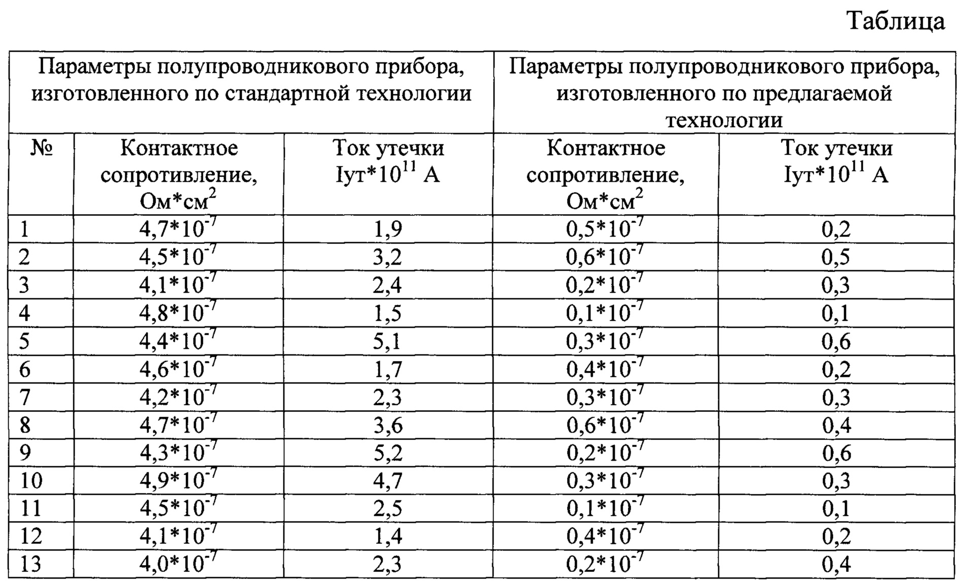
Экспериментальные исследования показали, что выход годных структур на партии пластин, сформированных в оптимальном режиме, увеличился на 14,7%.Experimental studies have shown that the yield of structures on a batch of plates, formed in the optimal mode, increased by 14.7%.
Предложенный способ изготовления полупроводникового прибора формированием слоя силицида палладия Pd2Si путем нанесения электроннолучевым распылением пленки палладия толщиной 50 нм в вакууме 2,7*10-5 Па, со скоростью осаждения 0,5 нм/с, при температуре подложки 100°C с последующей термообработки при температуре 250°C в течение 30 мин. в инертной среде, позволяет повысит процент выхода годных приборов и улучшит их надежность.The proposed method of manufacturing a semiconductor device by forming a layer of palladium silicide Pd2Si by applying electron-beam sputtering of a film of palladium 50 nm thick in vacuum 2.7 * 10 -5 Pa, with a deposition rate of 0.5 nm / s, at a substrate temperature of 100 ° C, followed by heat treatment temperature of 250 ° C for 30 min. in an inert environment, allows you to increase the percentage of yield devices and improve their reliability.
Технический результат: снижение контактного сопротивления, обеспечение технологичности, улучшение параметров структур, повышение качества и увеличения процента выхода годных.Technical result: reduction of contact resistance, ensuring manufacturability, improving the parameters of structures, improving quality and increasing the percentage of yield.
Claims (1)
Priority Applications (1)
| Application Number | Priority Date | Filing Date | Title |
|---|---|---|---|
| RU2018108935A RU2688861C1 (en) | 2018-03-12 | 2018-03-12 | Semiconductor device manufacturing method |
Applications Claiming Priority (1)
| Application Number | Priority Date | Filing Date | Title |
|---|---|---|---|
| RU2018108935A RU2688861C1 (en) | 2018-03-12 | 2018-03-12 | Semiconductor device manufacturing method |
Publications (1)
| Publication Number | Publication Date |
|---|---|
| RU2688861C1 true RU2688861C1 (en) | 2019-05-22 |
Family
ID=66636946
Family Applications (1)
| Application Number | Title | Priority Date | Filing Date |
|---|---|---|---|
| RU2018108935A RU2688861C1 (en) | 2018-03-12 | 2018-03-12 | Semiconductor device manufacturing method |
Country Status (1)
| Country | Link |
|---|---|
| RU (1) | RU2688861C1 (en) |
Cited By (1)
| Publication number | Priority date | Publication date | Assignee | Title |
|---|---|---|---|---|
| RU2786689C1 (en) * | 2022-02-02 | 2022-12-23 | Федеральное государственное бюджетное образовательное учреждение высшего образования "Кабардино-Балкарский государственный университет им. Х.М. Бербекова" (КБГУ) | Method for formation of silicide |
Citations (7)
| Publication number | Priority date | Publication date | Assignee | Title |
|---|---|---|---|---|
| US7229920B2 (en) * | 2005-01-11 | 2007-06-12 | United Microelectronics Corp. | Method of fabricating metal silicide layer |
| RU2006114833A (en) * | 2003-10-03 | 2007-11-10 | Спиннэйкер Семикондактор, Инк. (Us) | METHOD FOR PRODUCING A MOSFET FIELD TRANSISTOR WITH A SCHOTKI BARRIER USING THE ISOTROPIC ETCHING PROCESS |
| RU2369669C2 (en) * | 2007-08-09 | 2009-10-10 | Сабир Абенович Айтхожин | Substrate for growing of epitaxial layers of gallium nitride |
| RU2392688C1 (en) * | 2009-05-20 | 2010-06-20 | Федеральное агентство по образованию Государственное образовательное учреждение высшего профессионального образования Рязанский государственный радиотехнический университет | Method of making ohmic contacts in thin-film devices on amorphous undoped semiconductors |
| US20120181636A1 (en) * | 2007-07-17 | 2012-07-19 | Aditi Chandra | Printing of Contact Metal and Interconnect Metal Via Seed Printing and Plating |
| RU2591237C1 (en) * | 2015-05-20 | 2016-07-20 | Федеральное государственное бюджетное образовательное учреждение высшего образования "Чеченский государственный университет" (ФГБОУ ВО "Чеченский государственный университет") | Method of making semiconductor device |
| RU2610056C1 (en) * | 2015-11-19 | 2017-02-07 | Федеральное государственное бюджетное образовательное учреждение высшего образования Чеченский государственный университет (ФГБОУ ВО "Чеченский государственный университет") | Method of making semiconductor device |
-
2018
- 2018-03-12 RU RU2018108935A patent/RU2688861C1/en not_active IP Right Cessation
Patent Citations (7)
| Publication number | Priority date | Publication date | Assignee | Title |
|---|---|---|---|---|
| RU2006114833A (en) * | 2003-10-03 | 2007-11-10 | Спиннэйкер Семикондактор, Инк. (Us) | METHOD FOR PRODUCING A MOSFET FIELD TRANSISTOR WITH A SCHOTKI BARRIER USING THE ISOTROPIC ETCHING PROCESS |
| US7229920B2 (en) * | 2005-01-11 | 2007-06-12 | United Microelectronics Corp. | Method of fabricating metal silicide layer |
| US20120181636A1 (en) * | 2007-07-17 | 2012-07-19 | Aditi Chandra | Printing of Contact Metal and Interconnect Metal Via Seed Printing and Plating |
| RU2369669C2 (en) * | 2007-08-09 | 2009-10-10 | Сабир Абенович Айтхожин | Substrate for growing of epitaxial layers of gallium nitride |
| RU2392688C1 (en) * | 2009-05-20 | 2010-06-20 | Федеральное агентство по образованию Государственное образовательное учреждение высшего профессионального образования Рязанский государственный радиотехнический университет | Method of making ohmic contacts in thin-film devices on amorphous undoped semiconductors |
| RU2591237C1 (en) * | 2015-05-20 | 2016-07-20 | Федеральное государственное бюджетное образовательное учреждение высшего образования "Чеченский государственный университет" (ФГБОУ ВО "Чеченский государственный университет") | Method of making semiconductor device |
| RU2610056C1 (en) * | 2015-11-19 | 2017-02-07 | Федеральное государственное бюджетное образовательное учреждение высшего образования Чеченский государственный университет (ФГБОУ ВО "Чеченский государственный университет") | Method of making semiconductor device |
Cited By (2)
| Publication number | Priority date | Publication date | Assignee | Title |
|---|---|---|---|---|
| RU2786689C1 (en) * | 2022-02-02 | 2022-12-23 | Федеральное государственное бюджетное образовательное учреждение высшего образования "Кабардино-Балкарский государственный университет им. Х.М. Бербекова" (КБГУ) | Method for formation of silicide |
| RU2851680C1 (en) * | 2025-06-18 | 2025-11-27 | Федеральное государственное бюджетное образовательное учреждение высшего образования "Кабардино-Балкарский государственный университет им. Х.М. Бербекова" (КБГУ) | Method for manufacturing semiconductor device |
Similar Documents
| Publication | Publication Date | Title |
|---|---|---|
| US20090134402A1 (en) | Silicon carbide mos field-effect transistor and process for producing the same | |
| US10553719B2 (en) | Semiconductor devices and fabrication method thereof | |
| CN110660643A (en) | Method for optimizing passivation of gallium nitride high electron mobility transistor | |
| WO2011160591A1 (en) | Vdmos device and manufacturing method thereof | |
| US10032894B2 (en) | Silicon carbide semiconductor device and method of manufacturing silicon carbide semiconductor device | |
| CN103597582B (en) | Nitride semiconductor device and method for manufacturing same | |
| JP6562559B2 (en) | Gallium nitride field effect transistor | |
| CN108598154A (en) | Enhanced gallium nitride transistor and preparation method thereof | |
| RU2584273C1 (en) | Method of making semiconductor device | |
| RU2688861C1 (en) | Semiconductor device manufacturing method | |
| TW201330253A (en) | Metal oxide semiconductor field effect electro-crystal volume circuit with improved telluride thickness uniformity and manufacturing method thereof | |
| RU2688874C1 (en) | Semiconductor device manufacturing method | |
| KR20110067512A (en) | Enhancement normally off nitride semiconductor device and manufacturing method thereof | |
| JP6690333B2 (en) | Silicon carbide semiconductor device and method for manufacturing silicon carbide semiconductor device | |
| RU2688851C1 (en) | Semiconductor device manufacturing method | |
| RU2674413C1 (en) | Method for making semiconductor device | |
| RU2734094C1 (en) | Semiconductor device manufacturing method | |
| CN113178384B (en) | SiC-based ohmic contact structure and method for manufacturing same | |
| RU2822580C1 (en) | Semiconductor device manufacturing method | |
| RU2818689C1 (en) | Semiconductor device manufacturing method | |
| RU2515334C1 (en) | Method of making thin-film transistor | |
| RU2719622C1 (en) | Semiconductor device manufacturing method | |
| RU2610056C1 (en) | Method of making semiconductor device | |
| RU2833580C1 (en) | Semiconductor device manufacturing method | |
| RU2748455C1 (en) | Method for manufacturing semiconductor device |
Legal Events
| Date | Code | Title | Description |
|---|---|---|---|
| MM4A | The patent is invalid due to non-payment of fees |
Effective date: 20200313 |