RU2748455C1 - Method for manufacturing semiconductor device - Google Patents
Method for manufacturing semiconductor device Download PDFInfo
- Publication number
- RU2748455C1 RU2748455C1 RU2020123351A RU2020123351A RU2748455C1 RU 2748455 C1 RU2748455 C1 RU 2748455C1 RU 2020123351 A RU2020123351 A RU 2020123351A RU 2020123351 A RU2020123351 A RU 2020123351A RU 2748455 C1 RU2748455 C1 RU 2748455C1
- Authority
- RU
- Russia
- Prior art keywords
- field
- gate dielectric
- effect transistor
- semiconductor device
- technology
- Prior art date
Links
- 238000000034 method Methods 0.000 title claims abstract description 13
- 238000004519 manufacturing process Methods 0.000 title claims abstract description 11
- 239000004065 semiconductor Substances 0.000 title claims abstract description 6
- 230000005669 field effect Effects 0.000 claims abstract description 11
- VQCBHWLJZDBHOS-UHFFFAOYSA-N erbium(iii) oxide Chemical compound O=[Er]O[Er]=O VQCBHWLJZDBHOS-UHFFFAOYSA-N 0.000 claims abstract description 8
- 230000008021 deposition Effects 0.000 claims abstract description 5
- 238000000137 annealing Methods 0.000 claims abstract description 4
- 238000005566 electron beam evaporation Methods 0.000 claims abstract description 4
- 230000003647 oxidation Effects 0.000 claims abstract description 4
- 238000007254 oxidation reaction Methods 0.000 claims abstract description 4
- 230000000694 effects Effects 0.000 abstract description 2
- 230000005611 electricity Effects 0.000 abstract 1
- 239000000126 substance Substances 0.000 abstract 1
- 230000015572 biosynthetic process Effects 0.000 description 3
- XUIMIQQOPSSXEZ-UHFFFAOYSA-N Silicon Chemical compound [Si] XUIMIQQOPSSXEZ-UHFFFAOYSA-N 0.000 description 2
- 238000005530 etching Methods 0.000 description 2
- 229910052710 silicon Inorganic materials 0.000 description 2
- 239000010703 silicon Substances 0.000 description 2
- 229910052691 Erbium Inorganic materials 0.000 description 1
- OAICVXFJPJFONN-UHFFFAOYSA-N Phosphorus Chemical compound [P] OAICVXFJPJFONN-UHFFFAOYSA-N 0.000 description 1
- 230000007547 defect Effects 0.000 description 1
- 238000009792 diffusion process Methods 0.000 description 1
- UYAHIZSMUZPPFV-UHFFFAOYSA-N erbium Chemical group [Er] UYAHIZSMUZPPFV-UHFFFAOYSA-N 0.000 description 1
- 238000002513 implantation Methods 0.000 description 1
- 239000012535 impurity Substances 0.000 description 1
- 229910052698 phosphorus Inorganic materials 0.000 description 1
- 239000011574 phosphorus Substances 0.000 description 1
- 238000001020 plasma etching Methods 0.000 description 1
- 229910021420 polycrystalline silicon Inorganic materials 0.000 description 1
- 229920005591 polysilicon Polymers 0.000 description 1
- 230000001681 protective effect Effects 0.000 description 1
- 230000007704 transition Effects 0.000 description 1
- 235000012431 wafers Nutrition 0.000 description 1
Classifications
-
- H—ELECTRICITY
- H10—SEMICONDUCTOR DEVICES; ELECTRIC SOLID-STATE DEVICES NOT OTHERWISE PROVIDED FOR
- H10D—INORGANIC ELECTRIC SEMICONDUCTOR DEVICES
- H10D64/00—Electrodes of devices having potential barriers
- H10D64/60—Electrodes characterised by their materials
- H10D64/66—Electrodes having a conductor capacitively coupled to a semiconductor by an insulator, e.g. MIS electrodes
Landscapes
- Thin Film Transistor (AREA)
Abstract
Description
Изобретение относится к области технологии производства полупроводниковых приборов, в частности к технологии изготовления подзатворного диэлектрика полевого транзистора с пониженным значением тока утечки.The invention relates to the field of technology for the production of semiconductor devices, in particular to the technology of manufacturing a gate dielectric of a field-effect transistor with a reduced value of the leakage current.
Известен способ изготовления полевого транзистора [Пат. №5145798 США, МКИ H01L 21/336] с изолированным затвором. В процессе изготовления полевого транзистора для создания n+ областей истока и стока применяются формирование оксидных боковых стенок затвора с помощью травления, имплантирование фосфора Р и горизонтальная диффузия. В результате под стенками - спейсерами создаются переходные области с плавно изменяющейся концентрацией примесей, расположенные между n+ областями истока и стока и каналом. В таких приборах из-за не технологичности формирование оксидных боковых стенок затвора применением процесса травления образуется большое количество дефектов, которые ухудшают электрические параметры приборов.A known method of manufacturing a field-effect transistor [US Pat. No. 5145798 USA, MKI H01L 21/336] with an insulated gate. In the process of manufacturing a field-effect transistor, the formation of oxide side walls of the gate by etching, implantation of phosphorus P, and horizontal diffusion are used to create n + source and drain regions. As a result, transition regions with a smoothly varying concentration of impurities are created under the walls - spacers, located between the n + regions of the source and drain and the channel. In such devices, due to the lack of manufacturability, the formation of oxide side walls of the gate using the etching process forms a large number of defects that worsen the electrical parameters of the devices.
Известен способ изготовления полевого транзистора [Пат. №5134452 США, МКИ H01L 29/78] с затворным изолирующим слоем. Изготовление полевого транзистора на толстом защитном слое оксида и на открытой поверхности кремния с областями истока и стока осаждается слой проводящего поликремния, из которого затем формируются электроды стока и стока. После вскрытия канальной области проводится реактивное ионное травление с образованием шероховатой поверхности с размерами неровностей до 50 нм. Затем над канальной областью с помощью ПФХО создается тонкий затворный оксид и формируется затвор.A known method of manufacturing a field-effect transistor [US Pat. No. 5134452 USA, MKI H01L 29/78] with a gate insulating layer. Manufacturing a field-effect transistor on a thick protective oxide layer and on an open silicon surface with source and drain regions, a conductive polysilicon layer is deposited, from which drain and drain electrodes are then formed. After opening the channel region, reactive ion etching is carried out with the formation of a rough surface with irregularities up to 50 nm. Then, a thin gate oxide is created over the channel region with the help of PPCO, and a gate is formed.
Недостатками этого способа являются:The disadvantages of this method are:
- высокие значения токов утечек;- high values of leakage currents;
- высокая дефектность;- high defectiveness;
- низкая технологичность.- low manufacturability.
Задача, решаемая изобретением: снижение токов утечек, обеспечение технологичности, улучшение параметров приборов, повышение качества и увеличение процента выхода годных.The problem solved by the invention: reducing leakage currents, ensuring manufacturability, improving the parameters of devices, improving quality and increasing the percentage of yield.
Задача решается тем, что подзатворный диэлектрик полевого транзистора формируется на основе оксида эрбия методом электроннолучевого испарения в вакууме 1*10-6 Па со скоростью осаждения 0,1 нм/с, толщиной 25 нм, с последующим окислением при температуре 600-700°С и отжигом в атмосфере 60% N2 - 40% Н2 в течение 20 мин.The problem is solved by the fact that the gate dielectric of the field-effect transistor is formed on the basis of erbium oxide by the method of electron-beam evaporation in a vacuum of 1 * 10 -6 Pa with a deposition rate of 0.1 nm / s, 25 nm thick, followed by oxidation at a temperature of 600-700 ° C and annealing in an atmosphere of 60% N 2 - 40% H 2 for 20 min.
Технология способа состоит в следующем: подзатворный диэлектрик полевого транзистора формируется на основе оксида эрбия на пластинах кремния р-типа проводимости с ориентацией (100), с удельным сопротивлением 10 Ом* см, нанесением эрбия методом электронно-лучевого испарения в вакууме 1*10-6 Па со скоростью осаждения 0,1 нм/с, толщиной 25 нм, с последующим окислением при температуре 600-700°С и отжигом в атмосфере 60% N2 - 40% Н2 в течение 20 мин. Активные области n-канального полевого транзистора и электроды к ним формировали по стандартной технологии.The technology of the method is as follows: the gate dielectric of the field-effect transistor is formed on the basis of erbium oxide on p-type silicon wafers with the orientation (100), with a resistivity of 10 Ohm * cm, the deposition of erbium by the method of electron beam evaporation in a vacuum 1 * 10 -6 Pa with a deposition rate of 0.1 nm / s, a thickness of 25 nm, followed by oxidation at a temperature of 600-700 ° C and annealing in an atmosphere of 60% N 2 - 40% H 2 for 20 minutes. The active regions of the n-channel field-effect transistor and the electrodes to them were formed according to the standard technology.
По предлагаемому способу были изготовлены и исследованы полупроводниковые приборы. Результаты обработки представлены в таблице.According to the proposed method, semiconductor devices were manufactured and investigated. The processing results are presented in the table.

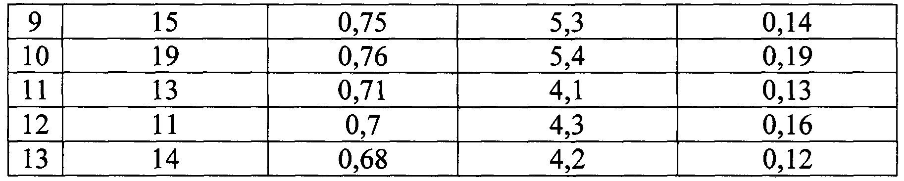
Экспериментальные исследования показали, что выход годных структур на партии пластин, сформированных в оптимальном режиме, увеличился на 19,2%.Experimental studies have shown that the yield of suitable structures for batches of plates formed in the optimal mode increased by 19.2%.
Технический результат: снижение токов утечек, обеспечение технологичности, улучшение параметров приборов, повышение качества и увеличения процента выхода годных.EFFECT: reducing leakage currents, ensuring manufacturability, improving the parameters of devices, improving the quality and increasing the percentage of yield.
Стабильность параметров во всем эксплуатационном интервале температур была нормальной и соответствовала требованиям.The stability of the parameters over the entire operating temperature range was normal and met the requirements.
Claims (1)
Priority Applications (1)
| Application Number | Priority Date | Filing Date | Title |
|---|---|---|---|
| RU2020123351A RU2748455C1 (en) | 2020-07-08 | 2020-07-08 | Method for manufacturing semiconductor device |
Applications Claiming Priority (1)
| Application Number | Priority Date | Filing Date | Title |
|---|---|---|---|
| RU2020123351A RU2748455C1 (en) | 2020-07-08 | 2020-07-08 | Method for manufacturing semiconductor device |
Publications (1)
| Publication Number | Publication Date |
|---|---|
| RU2748455C1 true RU2748455C1 (en) | 2021-05-25 |
Family
ID=76033985
Family Applications (1)
| Application Number | Title | Priority Date | Filing Date |
|---|---|---|---|
| RU2020123351A RU2748455C1 (en) | 2020-07-08 | 2020-07-08 | Method for manufacturing semiconductor device |
Country Status (1)
| Country | Link |
|---|---|
| RU (1) | RU2748455C1 (en) |
Cited By (1)
| Publication number | Priority date | Publication date | Assignee | Title |
|---|---|---|---|---|
| RU2851680C1 (en) * | 2025-06-18 | 2025-11-27 | Федеральное государственное бюджетное образовательное учреждение высшего образования "Кабардино-Балкарский государственный университет им. Х.М. Бербекова" (КБГУ) | Method for manufacturing semiconductor device |
Citations (4)
| Publication number | Priority date | Publication date | Assignee | Title |
|---|---|---|---|---|
| US5134452A (en) * | 1990-04-03 | 1992-07-28 | Mitsubishi Denki Kabushiki Kaisha | MIS type FET semiconductor device with gate insulating layer having a high dielectric breakdown strength |
| RU2606780C1 (en) * | 2015-06-09 | 2017-01-10 | Федеральное государственное бюджетное образовательное учреждение высшего образования "Кабардино-Балкарский государственный университет им. Х.М. Бербекова" (КБГУ) | Method of making a semiconductor device |
| RU2630708C1 (en) * | 2013-10-30 | 2017-09-12 | Рикох Компани, Лтд. | Field transistor, display element, image display device and system |
| RU2677500C1 (en) * | 2018-03-07 | 2019-01-17 | Федеральное государственное бюджетное образовательное учреждение высшего образования "Чеченский государственный университет" | Method for making semiconductor device |
-
2020
- 2020-07-08 RU RU2020123351A patent/RU2748455C1/en active
Patent Citations (4)
| Publication number | Priority date | Publication date | Assignee | Title |
|---|---|---|---|---|
| US5134452A (en) * | 1990-04-03 | 1992-07-28 | Mitsubishi Denki Kabushiki Kaisha | MIS type FET semiconductor device with gate insulating layer having a high dielectric breakdown strength |
| RU2630708C1 (en) * | 2013-10-30 | 2017-09-12 | Рикох Компани, Лтд. | Field transistor, display element, image display device and system |
| RU2606780C1 (en) * | 2015-06-09 | 2017-01-10 | Федеральное государственное бюджетное образовательное учреждение высшего образования "Кабардино-Балкарский государственный университет им. Х.М. Бербекова" (КБГУ) | Method of making a semiconductor device |
| RU2677500C1 (en) * | 2018-03-07 | 2019-01-17 | Федеральное государственное бюджетное образовательное учреждение высшего образования "Чеченский государственный университет" | Method for making semiconductor device |
Cited By (1)
| Publication number | Priority date | Publication date | Assignee | Title |
|---|---|---|---|---|
| RU2851680C1 (en) * | 2025-06-18 | 2025-11-27 | Федеральное государственное бюджетное образовательное учреждение высшего образования "Кабардино-Балкарский государственный университет им. Х.М. Бербекова" (КБГУ) | Method for manufacturing semiconductor device |
Similar Documents
| Publication | Publication Date | Title |
|---|---|---|
| RU2584273C1 (en) | Method of making semiconductor device | |
| RU2748455C1 (en) | Method for manufacturing semiconductor device | |
| RU2671294C1 (en) | Method for making semiconductor device | |
| RU2522930C2 (en) | Method of thin film transistor manufacturing | |
| RU2734094C1 (en) | Semiconductor device manufacturing method | |
| RU2674413C1 (en) | Method for making semiconductor device | |
| RU2688851C1 (en) | Semiconductor device manufacturing method | |
| RU2633799C1 (en) | Method of manufacturing semiconductor device | |
| RU2596861C1 (en) | Method of making semiconductor device | |
| RU2515334C1 (en) | Method of making thin-film transistor | |
| RU2723982C1 (en) | Semiconductor device manufacturing method | |
| RU2854732C1 (en) | Method for manufacturing a semiconductor device | |
| RU2757177C1 (en) | Method for manufacturing silicide contacts from tungsten | |
| RU2851680C1 (en) | Method for manufacturing semiconductor device | |
| RU2688881C1 (en) | Semiconductor device manufacturing method | |
| RU2798455C1 (en) | Method for manufacturing thin film transistor | |
| RU2831677C1 (en) | Method of manufacturing semiconductor device with low-doped drains | |
| RU2752125C1 (en) | Method for manufacturing semiconductor device | |
| RU2818689C1 (en) | Semiconductor device manufacturing method | |
| RU2688864C1 (en) | Semiconductor device manufacturing method | |
| RU2693506C1 (en) | Semiconductor device manufacturing method | |
| RU2822580C1 (en) | Semiconductor device manufacturing method | |
| RU2709603C1 (en) | Semiconductor device manufacturing method | |
| RU2836128C1 (en) | Method of making radiation-resistant semiconductor device | |
| RU2610056C1 (en) | Method of making semiconductor device |