KR20250031165A - Semiconductor device and manufacturing method of the same - Google Patents
Semiconductor device and manufacturing method of the same Download PDFInfo
- Publication number
- KR20250031165A KR20250031165A KR1020250020674A KR20250020674A KR20250031165A KR 20250031165 A KR20250031165 A KR 20250031165A KR 1020250020674 A KR1020250020674 A KR 1020250020674A KR 20250020674 A KR20250020674 A KR 20250020674A KR 20250031165 A KR20250031165 A KR 20250031165A
- Authority
- KR
- South Korea
- Prior art keywords
- film
- oxide semiconductor
- addition
- semiconductor film
- insulating film
- Prior art date
- Legal status (The legal status is an assumption and is not a legal conclusion. Google has not performed a legal analysis and makes no representation as to the accuracy of the status listed.)
- Granted
Links
Images


Classifications
-
- H—ELECTRICITY
- H10—SEMICONDUCTOR DEVICES; ELECTRIC SOLID-STATE DEVICES NOT OTHERWISE PROVIDED FOR
- H10D—INORGANIC ELECTRIC SEMICONDUCTOR DEVICES
- H10D86/00—Integrated devices formed in or on insulating or conducting substrates, e.g. formed in silicon-on-insulator [SOI] substrates or on stainless steel or glass substrates
- H10D86/40—Integrated devices formed in or on insulating or conducting substrates, e.g. formed in silicon-on-insulator [SOI] substrates or on stainless steel or glass substrates characterised by multiple TFTs
- H10D86/421—Integrated devices formed in or on insulating or conducting substrates, e.g. formed in silicon-on-insulator [SOI] substrates or on stainless steel or glass substrates characterised by multiple TFTs having a particular composition, shape or crystalline structure of the active layer
- H10D86/423—Integrated devices formed in or on insulating or conducting substrates, e.g. formed in silicon-on-insulator [SOI] substrates or on stainless steel or glass substrates characterised by multiple TFTs having a particular composition, shape or crystalline structure of the active layer comprising semiconductor materials not belonging to the Group IV, e.g. InGaZnO
-
- G—PHYSICS
- G02—OPTICS
- G02F—OPTICAL DEVICES OR ARRANGEMENTS FOR THE CONTROL OF LIGHT BY MODIFICATION OF THE OPTICAL PROPERTIES OF THE MEDIA OF THE ELEMENTS INVOLVED THEREIN; NON-LINEAR OPTICS; FREQUENCY-CHANGING OF LIGHT; OPTICAL LOGIC ELEMENTS; OPTICAL ANALOGUE/DIGITAL CONVERTERS
- G02F1/00—Devices or arrangements for the control of the intensity, colour, phase, polarisation or direction of light arriving from an independent light source, e.g. switching, gating or modulating; Non-linear optics
- G02F1/01—Devices or arrangements for the control of the intensity, colour, phase, polarisation or direction of light arriving from an independent light source, e.g. switching, gating or modulating; Non-linear optics for the control of the intensity, phase, polarisation or colour
- G02F1/13—Devices or arrangements for the control of the intensity, colour, phase, polarisation or direction of light arriving from an independent light source, e.g. switching, gating or modulating; Non-linear optics for the control of the intensity, phase, polarisation or colour based on liquid crystals, e.g. single liquid crystal display cells
- G02F1/133—Constructional arrangements; Operation of liquid crystal cells; Circuit arrangements
- G02F1/136—Liquid crystal cells structurally associated with a semi-conducting layer or substrate, e.g. cells forming part of an integrated circuit
- G02F1/1362—Active matrix addressed cells
- G02F1/1368—Active matrix addressed cells in which the switching element is a three-electrode device
-
- H—ELECTRICITY
- H10—SEMICONDUCTOR DEVICES; ELECTRIC SOLID-STATE DEVICES NOT OTHERWISE PROVIDED FOR
- H10D—INORGANIC ELECTRIC SEMICONDUCTOR DEVICES
- H10D1/00—Resistors, capacitors or inductors
- H10D1/60—Capacitors
- H10D1/68—Capacitors having no potential barriers
- H10D1/692—Electrodes
-
- H—ELECTRICITY
- H10—SEMICONDUCTOR DEVICES; ELECTRIC SOLID-STATE DEVICES NOT OTHERWISE PROVIDED FOR
- H10D—INORGANIC ELECTRIC SEMICONDUCTOR DEVICES
- H10D30/00—Field-effect transistors [FET]
- H10D30/60—Insulated-gate field-effect transistors [IGFET]
- H10D30/67—Thin-film transistors [TFT]
- H10D30/6704—Thin-film transistors [TFT] having supplementary regions or layers in the thin films or in the insulated bulk substrates for controlling properties of the device
-
- H—ELECTRICITY
- H10—SEMICONDUCTOR DEVICES; ELECTRIC SOLID-STATE DEVICES NOT OTHERWISE PROVIDED FOR
- H10D—INORGANIC ELECTRIC SEMICONDUCTOR DEVICES
- H10D30/00—Field-effect transistors [FET]
- H10D30/60—Insulated-gate field-effect transistors [IGFET]
- H10D30/67—Thin-film transistors [TFT]
- H10D30/6729—Thin-film transistors [TFT] characterised by the electrodes
- H10D30/673—Thin-film transistors [TFT] characterised by the electrodes characterised by the shapes, relative sizes or dispositions of the gate electrodes
- H10D30/6733—Multi-gate TFTs
- H10D30/6734—Multi-gate TFTs having gate electrodes arranged on both top and bottom sides of the channel, e.g. dual-gate TFTs
-
- H—ELECTRICITY
- H10—SEMICONDUCTOR DEVICES; ELECTRIC SOLID-STATE DEVICES NOT OTHERWISE PROVIDED FOR
- H10D—INORGANIC ELECTRIC SEMICONDUCTOR DEVICES
- H10D30/00—Field-effect transistors [FET]
- H10D30/60—Insulated-gate field-effect transistors [IGFET]
- H10D30/67—Thin-film transistors [TFT]
- H10D30/6729—Thin-film transistors [TFT] characterised by the electrodes
- H10D30/6737—Thin-film transistors [TFT] characterised by the electrodes characterised by the electrode materials
- H10D30/6739—Conductor-insulator-semiconductor electrodes
-
- H—ELECTRICITY
- H10—SEMICONDUCTOR DEVICES; ELECTRIC SOLID-STATE DEVICES NOT OTHERWISE PROVIDED FOR
- H10D—INORGANIC ELECTRIC SEMICONDUCTOR DEVICES
- H10D30/00—Field-effect transistors [FET]
- H10D30/60—Insulated-gate field-effect transistors [IGFET]
- H10D30/67—Thin-film transistors [TFT]
- H10D30/674—Thin-film transistors [TFT] characterised by the active materials
- H10D30/6755—Oxide semiconductors, e.g. zinc oxide, copper aluminium oxide or cadmium stannate
-
- H—ELECTRICITY
- H10—SEMICONDUCTOR DEVICES; ELECTRIC SOLID-STATE DEVICES NOT OTHERWISE PROVIDED FOR
- H10D—INORGANIC ELECTRIC SEMICONDUCTOR DEVICES
- H10D30/00—Field-effect transistors [FET]
- H10D30/60—Insulated-gate field-effect transistors [IGFET]
- H10D30/67—Thin-film transistors [TFT]
- H10D30/6758—Thin-film transistors [TFT] characterised by the insulating substrates
-
- H—ELECTRICITY
- H10—SEMICONDUCTOR DEVICES; ELECTRIC SOLID-STATE DEVICES NOT OTHERWISE PROVIDED FOR
- H10D—INORGANIC ELECTRIC SEMICONDUCTOR DEVICES
- H10D62/00—Semiconductor bodies, or regions thereof, of devices having potential barriers
- H10D62/40—Crystalline structures
-
- H—ELECTRICITY
- H10—SEMICONDUCTOR DEVICES; ELECTRIC SOLID-STATE DEVICES NOT OTHERWISE PROVIDED FOR
- H10D—INORGANIC ELECTRIC SEMICONDUCTOR DEVICES
- H10D62/00—Semiconductor bodies, or regions thereof, of devices having potential barriers
- H10D62/80—Semiconductor bodies, or regions thereof, of devices having potential barriers characterised by the materials
-
- H—ELECTRICITY
- H10—SEMICONDUCTOR DEVICES; ELECTRIC SOLID-STATE DEVICES NOT OTHERWISE PROVIDED FOR
- H10D—INORGANIC ELECTRIC SEMICONDUCTOR DEVICES
- H10D64/00—Electrodes of devices having potential barriers
- H10D64/60—Electrodes characterised by their materials
- H10D64/66—Electrodes having a conductor capacitively coupled to a semiconductor by an insulator, e.g. MIS electrodes
- H10D64/68—Electrodes having a conductor capacitively coupled to a semiconductor by an insulator, e.g. MIS electrodes characterised by the insulator, e.g. by the gate insulator
- H10D64/691—Electrodes having a conductor capacitively coupled to a semiconductor by an insulator, e.g. MIS electrodes characterised by the insulator, e.g. by the gate insulator comprising metallic compounds, e.g. metal oxides or metal silicates
-
- H—ELECTRICITY
- H10—SEMICONDUCTOR DEVICES; ELECTRIC SOLID-STATE DEVICES NOT OTHERWISE PROVIDED FOR
- H10D—INORGANIC ELECTRIC SEMICONDUCTOR DEVICES
- H10D64/00—Electrodes of devices having potential barriers
- H10D64/60—Electrodes characterised by their materials
- H10D64/66—Electrodes having a conductor capacitively coupled to a semiconductor by an insulator, e.g. MIS electrodes
- H10D64/68—Electrodes having a conductor capacitively coupled to a semiconductor by an insulator, e.g. MIS electrodes characterised by the insulator, e.g. by the gate insulator
- H10D64/693—Electrodes having a conductor capacitively coupled to a semiconductor by an insulator, e.g. MIS electrodes characterised by the insulator, e.g. by the gate insulator the insulator comprising nitrogen, e.g. nitrides, oxynitrides or nitrogen-doped materials
-
- H—ELECTRICITY
- H10—SEMICONDUCTOR DEVICES; ELECTRIC SOLID-STATE DEVICES NOT OTHERWISE PROVIDED FOR
- H10D—INORGANIC ELECTRIC SEMICONDUCTOR DEVICES
- H10D86/00—Integrated devices formed in or on insulating or conducting substrates, e.g. formed in silicon-on-insulator [SOI] substrates or on stainless steel or glass substrates
- H10D86/01—Manufacture or treatment
- H10D86/021—Manufacture or treatment of multiple TFTs
-
- H—ELECTRICITY
- H10—SEMICONDUCTOR DEVICES; ELECTRIC SOLID-STATE DEVICES NOT OTHERWISE PROVIDED FOR
- H10D—INORGANIC ELECTRIC SEMICONDUCTOR DEVICES
- H10D86/00—Integrated devices formed in or on insulating or conducting substrates, e.g. formed in silicon-on-insulator [SOI] substrates or on stainless steel or glass substrates
- H10D86/40—Integrated devices formed in or on insulating or conducting substrates, e.g. formed in silicon-on-insulator [SOI] substrates or on stainless steel or glass substrates characterised by multiple TFTs
- H10D86/481—Integrated devices formed in or on insulating or conducting substrates, e.g. formed in silicon-on-insulator [SOI] substrates or on stainless steel or glass substrates characterised by multiple TFTs integrated with passive devices, e.g. auxiliary capacitors
-
- H—ELECTRICITY
- H10—SEMICONDUCTOR DEVICES; ELECTRIC SOLID-STATE DEVICES NOT OTHERWISE PROVIDED FOR
- H10D—INORGANIC ELECTRIC SEMICONDUCTOR DEVICES
- H10D86/00—Integrated devices formed in or on insulating or conducting substrates, e.g. formed in silicon-on-insulator [SOI] substrates or on stainless steel or glass substrates
- H10D86/40—Integrated devices formed in or on insulating or conducting substrates, e.g. formed in silicon-on-insulator [SOI] substrates or on stainless steel or glass substrates characterised by multiple TFTs
- H10D86/60—Integrated devices formed in or on insulating or conducting substrates, e.g. formed in silicon-on-insulator [SOI] substrates or on stainless steel or glass substrates characterised by multiple TFTs wherein the TFTs are in active matrices
-
- H—ELECTRICITY
- H10—SEMICONDUCTOR DEVICES; ELECTRIC SOLID-STATE DEVICES NOT OTHERWISE PROVIDED FOR
- H10K—ORGANIC ELECTRIC SOLID-STATE DEVICES
- H10K59/00—Integrated devices, or assemblies of multiple devices, comprising at least one organic light-emitting element covered by group H10K50/00
- H10K59/10—OLED displays
- H10K59/12—Active-matrix OLED [AMOLED] displays
- H10K59/121—Active-matrix OLED [AMOLED] displays characterised by the geometry or disposition of pixel elements
- H10K59/1213—Active-matrix OLED [AMOLED] displays characterised by the geometry or disposition of pixel elements the pixel elements being TFTs
-
- H—ELECTRICITY
- H10—SEMICONDUCTOR DEVICES; ELECTRIC SOLID-STATE DEVICES NOT OTHERWISE PROVIDED FOR
- H10K—ORGANIC ELECTRIC SOLID-STATE DEVICES
- H10K59/00—Integrated devices, or assemblies of multiple devices, comprising at least one organic light-emitting element covered by group H10K50/00
- H10K59/10—OLED displays
- H10K59/12—Active-matrix OLED [AMOLED] displays
- H10K59/121—Active-matrix OLED [AMOLED] displays characterised by the geometry or disposition of pixel elements
- H10K59/1216—Active-matrix OLED [AMOLED] displays characterised by the geometry or disposition of pixel elements the pixel elements being capacitors
Landscapes
- Physics & Mathematics (AREA)
- Engineering & Computer Science (AREA)
- Microelectronics & Electronic Packaging (AREA)
- Nonlinear Science (AREA)
- Geometry (AREA)
- Chemical & Material Sciences (AREA)
- Crystallography & Structural Chemistry (AREA)
- Optics & Photonics (AREA)
- General Physics & Mathematics (AREA)
- Mathematical Physics (AREA)
- Thin Film Transistor (AREA)
- Devices For Indicating Variable Information By Combining Individual Elements (AREA)
- Liquid Crystal (AREA)
- Electroluminescent Light Sources (AREA)
- Metal-Oxide And Bipolar Metal-Oxide Semiconductor Integrated Circuits (AREA)
- Manufacturing & Machinery (AREA)
Abstract
개구율이 높은 반도체 장치를 제공한다.
질화 절연막과, 질화 절연막 위에 형성된 트랜지스터와, 질화 절연막 위에 형성된 한 쌍의 전극을 갖는 용량 소자를 갖고, 트랜지스터의 채널 형성 영역, 및 용량 소자의 한쪽의 전극은 산화물 반도체층으로 형성되고, 용량 소자의 다른 한쪽의 전극은 투광성 도전막으로 형성되고, 용량 소자의 한쪽의 전극은 질화 절연막에 접하고, 용량 소자의 다른 한쪽의 전극은 트랜지스터에 포함되는 소스 전극 또는 드레인 전극의 한쪽과 전기적으로 접속한다.Provides a semiconductor device with a high aperture ratio.
A capacitor having a nitride insulating film, a transistor formed on the nitride insulating film, and a pair of electrodes formed on the nitride insulating film, wherein a channel forming region of the transistor and one electrode of the capacitor are formed of an oxide semiconductor layer, the other electrode of the capacitor is formed of a light-transmitting conductive film, and one electrode of the capacitor is in contact with the nitride insulating film and the other electrode of the capacitor is electrically connected to one of a source electrode or a drain electrode included in the transistor.
Description
본 발명은 물건, 방법 또는 제조 방법에 관한 것이다. 또는, 본 발명은 프로세스, 머신, 매뉴팩처 또는 조성물(composition of matter)에 관한 것이다. 특히, 본 발명은, 예를 들면, 반도체 장치, 표시 장치, 발광 장치, 이들의 구동 방법 또는 이들의 제작 방법에 관한 것이다. 특히, 본 발명은, 예를 들면, 산화물 반도체를 포함하는 반도체 장치, 표시 장치 또는 발광 장치 및 그 제작 방법에 관한 것이다.The present invention relates to a thing, a method or a manufacturing method. Alternatively, the present invention relates to a process, a machine, a manufacture or a composition of matter. In particular, the present invention relates to, for example, a semiconductor device, a display device, a light-emitting device, a method for driving them or a method for manufacturing them. In particular, the present invention relates to, for example, a semiconductor device, a display device or a light-emitting device comprising an oxide semiconductor and a method for manufacturing them.
최근, 액정 디스플레이(LCD) 등의 플랫 패널 디스플레이가 널리 보급되고 있다. 플랫 패널 디스플레이 등의 표시 장치에 있어서, 행 방향 및 열 방향에 배치된 화소내에는 스위칭 소자인 트랜지스터와, 상기 트랜지스터와 전기적으로 접속된 액정 소자와, 상기 액정 소자와 병렬로 접속된 용량 소자가 설치되어 있다.Recently, flat panel displays such as liquid crystal displays (LCDs) have become widely popular. In display devices such as flat panel displays, pixels arranged in the row and column directions are provided with a transistor as a switching element, a liquid crystal element electrically connected to the transistor, and a capacitance element connected in parallel with the liquid crystal element.
상기 트랜지스터의 반도체막을 구성하는 반도체 재료로서는 아몰퍼스(amorphous, 비정질) 실리콘 또는 폴리(다결정) 실리콘 등의 실리콘 반도체가 범용되고 있다.As a semiconductor material constituting the semiconductor film of the above transistor, silicon semiconductors such as amorphous silicon or poly (polycrystalline) silicon are commonly used.
또한, 반도체 특성을 나타내는 금속 산화물(이하, 산화물 반도체라고 기재한다)은, 트랜지스터의 반도체막에 적용할 수 있는 반도체 재료이다. 예를 들면, 산화아연 또는 In-Ga-Zn계 산화물 반도체를 사용하여 트랜지스터를 제작하는 기술이 개시되어 있다(특허문헌 1 및 특허문헌 2를 참조).In addition, a metal oxide exhibiting semiconductor properties (hereinafter referred to as oxide semiconductor) is a semiconductor material that can be applied to a semiconductor film of a transistor. For example, a technology for manufacturing a transistor using zinc oxide or an In-Ga-Zn-based oxide semiconductor is disclosed (see
용량 소자는 한 쌍의 전극 사이에 유전체막이 설치되어 있고, 한 쌍의 전극 중 적어도 한쪽의 전극은, 트랜지스터를 구성하는 게이트(gate) 전극, 소스 전극 또는 드레인(drain) 전극 등과 동일 재료로 형성되기 때문에 금속 등의 차광성을 갖는 도전막으로 형성되어 있는 경우가 많다.The capacitor element has a dielectric film installed between a pair of electrodes, and at least one of the pair of electrodes is formed of the same material as the gate electrode, source electrode, or drain electrode that constitutes the transistor, so it is often formed of a conductive film with light-blocking properties such as metal.
또한, 용량 소자의 용량값을 크게 할수록 전계(電界)를 가한 상황에서, 액정 소자의 액정 분자의 배향을 일정하게 유지할 수 있는 기간을 길게 할 수 있다. 정지 화상을 표시시킬 수 있는 표시 장치에 있어서, 상기 기간을 길게 할 수 있는 것은 화상 데이터를 재기록하는 회수를 저감시킬 수 있어, 소비 전력의 저감이 기대된다.In addition, as the capacitance value of the capacitance element is increased, the period during which the alignment of the liquid crystal molecules of the liquid crystal element can be maintained constant in a situation where an electric field is applied can be increased. In a display device capable of displaying a still image, the ability to increase the period can reduce the number of times the image data is rewritten, and thus a reduction in power consumption is expected.
용량 소자의 전하 용량을 크게 하기 위하여는, 화소내에서의 용량 소자의 점유 면적을 크게 하는, 구체적으로는 한 쌍의 전극이 중첩되어 있는 면적을 크게 하는 수단이 있다. 그러나, 상기 표시 장치에 있어서, 한 쌍의 전극이 중첩되어 있는 면적을 크게 하기 위하여 차광성을 갖는 도전막의 면적을 크게 하면 화소의 개구율이 저감되고, 화상의 표시 품질이 저하된다.In order to increase the charge capacity of a capacitor, there is a means of increasing the area occupied by the capacitor within a pixel, specifically, increasing the area where a pair of electrodes overlap. However, in the display device, if the area of a light-blocking conductive film is increased in order to increase the area where a pair of electrodes overlap, the aperture ratio of the pixel is reduced and the display quality of the image deteriorates.
따라서, 상기 과제를 감안하여 본 발명의 일 양태는 개구율이 높은 반도체 장치 등을 제공하는 것을 목적중 하나로 한다. 또는, 전하 용량을 증대시키는 것이 가능한 용량 소자를 포함하는 반도체 장치 등을 제공하는 것을 목적중 하나로 한다. 또는, 포토리소그래피 공정의 마스크 매수를 삭감할 수 있는 반도체 장치 등을 제공하는 것을 목적중 하나로 한다. 또는, 오프 전류가 낮은 반도체 장치 등을 제공하는 것을 목적중 하나로 한다. 또는, 소비 전력을 저감시킨 반도체 장치 등을 제공하는 것을 목적중 하나로 한다. 또는, 투명한 반도체층을 사용한 반도체 장치 등을 제공하는 것을 목적중 하나로 한다. 또는, 신뢰성이 높은 반도체 장치 등을 제공하는 것을 목적중 하나로 한다. 또는, 눈이 편한 반도체 장치 등을 제공하는 것을 목적중 하나로 한다. 또는, 신규의 반도체 장치 등을 제공하는 것을 목적중 하나로 한다. 또는, 신규의 반도체 장치 등의 제작 방법을 제공하는 것을 목적중 하나로 한다.Accordingly, in consideration of the above problems, one aspect of the present invention has as one object the provision of a semiconductor device with a high aperture ratio. Or, one object the provision of a semiconductor device including a capacitance element capable of increasing charge capacity. Or, one object the provision of a semiconductor device capable of reducing the number of masks in a photolithography process. Or, one object the provision of a semiconductor device with low off-current. Or, one object the provision of a semiconductor device with reduced power consumption. Or, one object the provision of a semiconductor device using a transparent semiconductor layer. Or, one object the provision of a highly reliable semiconductor device. Or, one object the provision of a semiconductor device that is easy on the eyes. Or, one object the provision of a novel semiconductor device. Or, one object the provision of a method for manufacturing a novel semiconductor device.
또한, 이들 과제의 기재는 다른 과제의 존재를 방해하는 것이 아니다. 또한, 본 발명의 일 양태는 이들 과제의 전부를 해결할 필요는 없는 것으로 한다. 또한, 이들 이외의 과제는 명세서, 도면, 청구항 등의 기재로부터 저절로 명확해 지는 것이고, 명세서, 도면, 청구항 등의 기재로부터 이들 이외의 과제를 추출하는 것이 가능하다.In addition, the description of these tasks does not interfere with the existence of other tasks. In addition, it is not necessary for one aspect of the present invention to solve all of these tasks. In addition, tasks other than these are automatically clear from the description of the specification, drawings, claims, etc., and it is possible to extract tasks other than these from the description of the specification, drawings, claims, etc.
본 발명의 일 양태는, 산화물 반도체층을 한쪽의 전극으로 하고, 투광성 도전막을 다른 한쪽의 전극으로 하는 투광성을 갖는 용량 소자를 포함하는 반도체 장치에 관한 것이다.One aspect of the present invention relates to a semiconductor device including a light-transmitting capacitor having an oxide semiconductor layer as one electrode and a light-transmitting conductive film as the other electrode.
본 발명의 일 양태는 트랜지스터를 포함하는 반도체 장치이며, 제 1 절연막 위에 형성된 게이트 전극층, 제 1 배선 및 상기 제 1 배선과 전기적으로 접속된 제 1 산화물 반도체층과, 게이트 전극층 및 제 1 배선 위에 형성된 제 2 절연막과, 게이트 전극층과 중첩되고, 제 2 절연막 위에 형성된 제 2 산화물 반도체층과, 제 2 산화물 반도체층과 전기적으로 접속된 소스 전극층 및 드레인 전극층과, 제 1 산화물 반도체층, 제 2 산화물 반도체층, 제 2 절연막, 소스 전극층 및 드레인 전극층 위에 형성된 제 3 절연막과, 제 3 절연막 위에 형성된 제 4 절연막과, 제 1 산화물 반도체층 위에서, 제 4 절연막 위에 형성된 투광성 도전막을 갖고, 제 1 산화물 반도체층을 한쪽의 전극으로 하고, 제 3 절연막 및 제 4 절연막을 유전체로 하고, 투광성 도전막을 다른 한쪽의 전극으로 한 용량 소자를 포함하는 것을 특징으로 하는 반도체 장치이다.One aspect of the present invention is a semiconductor device including a transistor, characterized by including a capacitor having a gate electrode layer formed on a first insulating film, a first wiring, and a first oxide semiconductor layer electrically connected to the first wiring, a second insulating film formed on the gate electrode layer and the first wiring, a second oxide semiconductor layer overlapping the gate electrode layer and formed on the second insulating film, a source electrode layer and a drain electrode layer electrically connected to the second oxide semiconductor layer, a third insulating film formed on the first oxide semiconductor layer, the second oxide semiconductor layer, the second insulating film, the source electrode layer and the drain electrode layer, a fourth insulating film formed on the third insulating film, and a light-transmitting conductive film formed on the first oxide semiconductor layer and on the fourth insulating film, wherein the first oxide semiconductor layer serves as one electrode, the third insulating film and the fourth insulating film serve as dielectrics, and the light-transmitting conductive film serves as the other electrode.
제 1 산화물 반도체층 및 제 2 산화물 반도체층은 같은 재료로 형성되어 있는 것이 바람직하다.It is preferable that the first oxide semiconductor layer and the second oxide semiconductor layer are formed of the same material.
또한, 제 1 산화물 반도체층 및 제 2 산화물 반도체층은 에너지 갭이 2.0eV 이상인 것이 바람직하다.Additionally, it is preferable that the first oxide semiconductor layer and the second oxide semiconductor layer have an energy gap of 2.0 eV or more.
또한, 제 1 절연막은 질화산화실리콘, 질화실리콘, 질화알루미늄, 질화산화알루미늄 중에서 선택된 질화 절연 재료의 단층 구조 또는 적층 구조로 형성하는 것이 바람직하다.In addition, it is preferable that the first insulating film be formed as a single-layer structure or a laminated structure of a nitride insulating material selected from silicon nitride, silicon nitride, aluminum nitride, and aluminum nitride oxide.
또한, 제 3 절연막은 산화실리콘, 산화질화실리콘, 산화알루미늄, 산화하프늄, 산화갈륨 또는 Ga-Zn계 금속 산화물 중에서 선택된 산화 절연 재료의 단층 구조 또는 적층 구조로 형성하는 것이 바람직하다.In addition, it is preferable that the third insulating film be formed as a single-layer structure or a laminated structure of an oxide insulating material selected from among silicon oxide, silicon nitride oxide, aluminum oxide, hafnium oxide, gallium oxide, or Ga-Zn series metal oxide.
또한, 제 4 절연막은 질화산화실리콘, 질화실리콘, 질화알루미늄, 질화산화알루미늄 중에서 선택된 질화 절연 재료의 단층 구조 또는 적층 구조로 형성하는 것이 바람직하다.In addition, it is preferable that the fourth insulating film be formed as a single-layer structure or a laminated structure of a nitride insulating material selected from silicon nitride, silicon nitride, aluminum nitride, and aluminum nitride oxide.
또한, 게이트 전극층 및 제 1 배선은 같은 재료로 형성되어 있는 것이 바람직하다.Additionally, it is preferable that the gate electrode layer and the first wiring are formed of the same material.
또한, 투광성 도전막은 소스 전극 또는 드레인 전극의 한쪽과 전기적으로 접속되어 있는 구성으로 할 수 있다.Additionally, the light-transmitting conductive film may be configured to be electrically connected to one of the source electrode or the drain electrode.
또한, 제 1 배선과 제 1 산화물 반도체층은 직접 접함으로써 전기적으로 접속되는 구성으로 할 수 있다.In addition, the first wiring and the first oxide semiconductor layer can be configured to be electrically connected by direct contact.
또한, 제 1 배선과 제 1 산화물 반도체층은 제 2 배선을 통하여 접함으로써 전기적으로 접속되는 구성으로 할 수 있다.In addition, the first wiring and the first oxide semiconductor layer can be configured to be electrically connected by being in contact with each other through the second wiring.
또한, 본 발명의 다른 일 양태는 제 1 절연막 위에 게이트 전극층 및 제 1 배선을 형성하고, 제 1 절연막, 게이트 전극층 및 제 1 배선 위에 제 2 절연막을 형성하고, 제 2 절연막을 선택적으로 에칭하여 제 1 배선의 일부 및 제 1 절연막의 일부를 노출시키고, 노출된 제 1 배선의 일부 및 제 1 절연막의 일부 위에 제 1 산화물 반도체층, 게이트 전극층과 중첩되도록 제 2 절연막 위에 제 2 산화물 반도체층을 형성하고, 제 2 산화물 반도체층과 전기적으로 접속된 소스 전극층 및 드레인 전극층을 형성하고, 제 1 산화물 반도체층, 제 2 산화물 반도체층, 제 2 절연막, 소스 전극층 및 드레인 전극층 위에 제 3 절연막을 형성하고, 제 3 절연막 위에 제 4 절연막을 형성하고, 제 3 절연막 및 제 4 절연막에 소스 전극층 또는 드레인 전극층으로 통하는 개구부를 형성하고, 제 4 절연막 위에 개구부에서 소스 전극층 또는 드레인 전극층과 전기적으로 접속하고, 또한 제 1 산화물 반도체층과 중첩된 투광성 도전막을 형성하고, 트랜지스터와, 제 1 산화물 반도체층을 한쪽의 전극으로 하고, 제 3 절연막 및 제 4 절연막을 유전체로 하고, 투광성 도전막을 다른 한쪽의 전극으로 한 용량 소자를 형성하는 것을 특징으로 하는 반도체 장치의 제작 방법이다.In addition, another aspect of the present invention comprises: forming a gate electrode layer and a first wiring on a first insulating film, forming a second insulating film on the first insulating film, the gate electrode layer and the first wiring, selectively etching the second insulating film to expose a part of the first wiring and a part of the first insulating film, forming a second oxide semiconductor layer on the second insulating film so as to overlap with the first oxide semiconductor layer and the gate electrode layer on the exposed part of the first wiring and a part of the first insulating film, forming a source electrode layer and a drain electrode layer electrically connected to the second oxide semiconductor layer, forming a third insulating film on the first oxide semiconductor layer, the second oxide semiconductor layer, the second insulating film, the source electrode layer and the drain electrode layer, forming a fourth insulating film on the third insulating film, forming an opening communicating with the source electrode layer or the drain electrode layer in the third insulating film and the fourth insulating film, and forming the source electrode layer or the drain electrode layer in the opening on the fourth insulating film. A method for manufacturing a semiconductor device, characterized by forming a light-transmitting conductive film electrically connected to a drain electrode layer and overlapping a first oxide semiconductor layer, and forming a transistor and a capacitor element having the first oxide semiconductor layer as one electrode, a third insulating film and a fourth insulating film as dielectrics, and the light-transmitting conductive film as the other electrode.
제 1 산화물 반도체층 및 제 2 산화물 반도체층은 같은 재료로 형성하는 것이 바람직하다.It is preferable that the first oxide semiconductor layer and the second oxide semiconductor layer are formed of the same material.
또한, 제 1 산화물 반도체층 및 제 2 산화물 반도체층은 에너지 갭이 2.0eV 이상의 재료로 형성하는 것이 바람직하다.In addition, it is preferable that the first oxide semiconductor layer and the second oxide semiconductor layer be formed of a material having an energy gap of 2.0 eV or more.
또한, 제 1 절연막을 질화산화실리콘, 질화실리콘, 질화알루미늄, 질화산화알루미늄 중에서 선택된 질화 절연 재료의 단층 구조 또는 적층 구조로 형성하는 것이 바람직하다.In addition, it is preferable to form the first insulating film as a single-layer structure or a laminated structure of a nitride insulating material selected from silicon nitride, silicon nitride, aluminum nitride, and aluminum nitride oxide.
또한, 제 3 절연막을 산화실리콘, 산화질화실리콘, 산화알루미늄, 산화하프늄, 산화갈륨 또는 Ga-Zn계 금속 산화물 중에서 선택된 산화 절연 재료의 단층 구조 또는 적층 구조로 형성하는 것이 바람직하다.In addition, it is preferable to form the third insulating film in a single-layer structure or a laminated structure of an oxide insulating material selected from among silicon oxide, silicon nitride oxide, aluminum oxide, hafnium oxide, gallium oxide, or Ga-Zn series metal oxide.
또한, 제 4 절연막을 질화산화실리콘, 질화실리콘, 질화알루미늄, 질화산화알루미늄 중에서 선택된 질화 절연 재료의 단층 구조 또는 적층 구조로 형성하는 것이 바람직하다.In addition, it is preferable to form the fourth insulating film as a single-layer structure or a laminated structure of a nitride insulating material selected from silicon nitride, silicon nitride, aluminum nitride, and aluminum nitride oxide.
또한, 게이트 전극층 및 제 1 배선은 같은 재료로 형성하는 것이 바람직하다.Additionally, it is preferable that the gate electrode layer and the first wiring be formed of the same material.
또한, 제 1 배선과 제 1 산화물 반도체층은 직접 접하도록 형성하고, 전기적으로 접속할 수 있다.In addition, the first wiring and the first oxide semiconductor layer are formed to be in direct contact and can be electrically connected.
또한, 제 1 배선과 제 1 산화물 반도체층은 제 2 배선을 통하여 접하도록 형성하고, 전기적으로 접속하여도 좋다.Additionally, the first wiring and the first oxide semiconductor layer may be formed to be in contact with each other through the second wiring and may be electrically connected.
본 발명의 일 양태에서, 개구율이 높은 반도체 장치 등을 제공할 수 있다. 또는, 전하 용량을 증대시키는 것이 가능한 용량 소자를 갖는 반도체 장치 등을 제공할 수 있다. 또는, 포토리소그래피 공정의 마스크 매수를 삭감할 수 있는 반도체 장치 등을 제공할 수 있다. 또는, 오프 전류가 낮은 반도체 장치 등을 제공할 수 있다. 또는, 소비 전력을 저감시킨 반도체 장치 등을 제공할 수 있다. 또는, 투명한 반도체층을 사용한 반도체 장치 등을 제공할 수 있다. 또는, 신뢰성이 높은 반도체 장치 등을 제공할 수 있다. 또는, 눈이 편한 반도체 장치를 제공할 수 있다. 또는, 반도체 장치의 제작 방법을 제공할 수 있다.In one aspect of the present invention, a semiconductor device having a high aperture ratio can be provided. Or, a semiconductor device having a capacitive element capable of increasing charge capacity can be provided. Or, a semiconductor device capable of reducing the number of masks in a photolithography process can be provided. Or, a semiconductor device having a low off-current can be provided. Or, a semiconductor device having reduced power consumption can be provided. Or, a semiconductor device using a transparent semiconductor layer can be provided. Or, a highly reliable semiconductor device can be provided. Or, a semiconductor device that is easy on the eyes can be provided. Or, a method for manufacturing a semiconductor device can be provided.
도 1은 반도체 장치를 설명하는 상면도.
도 2는 반도체 장치를 설명하는 단면도.
도 3은 반도체 장치를 설명하는 도면.
도 4a 및 도 4b는 반도체 장치의 화소를 설명하는 회로도.
도 5a 및 도 5b는 반도체 장치의 제작 방법을 설명하는 단면도.
도 6a 및 도 6b는 반도체 장치의 제작 방법을 설명하는 단면도.
도 7은 반도체 장치의 용량 소자를 설명하는 단면도.
도 8은 반도체 장치를 설명하는 단면도.
도 9a 및 도 9b는 반도체 장치를 설명하는 단면도.
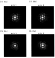
도 10a 및 도 10b는 산화물 반도체막의 극미(極微) 전자선 회절 패턴을 도시한 도면.
도 11a 및 도 11b는 산화물 반도체막의 CPM 측정 결과를 도시한 도면.
도 12는 CAAC-OS막의 CPM 측정 결과를 도시한 도면.
도 13a는 산화물 반도체막의 단면 TEM상이고, 도 13b 내지 도 13d는 극미 전자선 회절 패턴.
도 14a는 산화물 반도체막의 평면 TEM상이고, 도 14b는 제한 시야 전자선 회절 패턴.
도 15a 내지 도 15c는 전자선 회절 강도 분포의 개념도.
도 16은 석영 유리 기판의 극미 전자선 회절 패턴.
도 17은 산화물 반도체막의 극미 전자선 회절 패턴.
도 18a 및 도 18b는 산화물 반도체막의 단면 TEM상.
도 19는 산화물 반도체막의 X선 회절 분석 결과.
도 20은 CAAC-OS막의 단면 TEM상.
도 21a 내지 도 21d는 CAAC-OS막의 전자선 회절 패턴.
도 22는 CAAC-OS막의 단면 TEM상.
도 23a는 CAAC-OS막의 단면 TEM상이고, 도 23b는 X선 회절 스펙트럼.
도 24a 내지 도 24d는 CAAC-OS막의 전자선 회절 패턴.
도 25a는 CAAC-OS막의 단면 TEM상이고, 도 25b는 X선 회절 스펙트럼.
도 26a 내지 도 26d는 CAAC-OS막의 전자선 회절 패턴.
도 27a는 CAAC-OS막의 단면 TEM상이고, 도 27b는 X선 회절 스펙트럼.
도 28a 내지 도 28d는 CAAC-OS막의 전자선 회절 패턴.
도 29a 내지 도 29c는 반도체 장치를 설명하는 상면도.
도 30은 반도체 장치를 설명하는 단면도.
도 31a 및 도 31c는 반도체 장치를 설명하는 단면도이고, 31b는 상면도.
도 32는 표시 기능을 갖는 정보 처리 장치의 구성을 설명하는 블록도.
도 33a1 및 도 33a2는 정보 처리 장치의 표시부의 구성을 설명하는 블록도이고, 도 33b1 및 도 33b2는 회로도.
도 34a는 정보 처리 장치의 구성을 설명하는 블록도이고, 도 34b는 화상 데이터를 설명하기 위한 모식도.
도 35a1 및 도 35a2, 도 35b1 및 도 35b2는 정보 처리 장치의 효과를 설명하는 도면.
도 36은 정보 처리 장치를 설명하는 블록도.
도 37a 내지 도 37c는 반도체 장치를 사용한 전자 기기를 설명하는 도면.
도 38a 및 도 38b는 반도체 장치를 사용한 전자 기기를 설명하는 도면.
도 39a 내지 도 39c는 반도체 장치를 사용한 전자 기기를 설명하는 도면.Figure 1 is a top view illustrating a semiconductor device.
Figure 2 is a cross-sectional view illustrating a semiconductor device.
Figure 3 is a drawing explaining a semiconductor device.
FIGS. 4A and 4B are circuit diagrams illustrating pixels of a semiconductor device.
FIGS. 5a and 5b are cross-sectional views illustrating a method for manufacturing a semiconductor device.
Figures 6a and 6b are cross-sectional views illustrating a method for manufacturing a semiconductor device.
Figure 7 is a cross-sectional view illustrating a capacitive element of a semiconductor device.
Fig. 8 is a cross-sectional view illustrating a semiconductor device.
Figures 9a and 9b are cross-sectional views illustrating a semiconductor device.
Figures 10a and 10b are drawings showing ultra-fine electron diffraction patterns of an oxide semiconductor film.
Figures 11a and 11b are diagrams showing the results of CPM measurements of oxide semiconductor films.
Figure 12 is a diagram showing the CPM measurement results of a CAAC-OS film.
Figure 13a is a cross-sectional TEM image of an oxide semiconductor film, and Figures 13b to 13d are ultra-fine electron diffraction patterns.
Figure 14a is a planar TEM image of an oxide semiconductor film, and Figure 14b is a limited field electron diffraction pattern.
Figures 15a to 15c are conceptual diagrams of electron beam diffraction intensity distributions.
Figure 16 is an ultra-fine electron diffraction pattern of a quartz glass substrate.
Figure 17 is an ultra-fine electron diffraction pattern of an oxide semiconductor film.
Figures 18a and 18b are cross-sectional TEM images of an oxide semiconductor film.
Figure 19 shows the results of X-ray diffraction analysis of an oxide semiconductor film.
Figure 20 is a cross-sectional TEM image of a CAAC-OS film.
Figures 21a to 21d are electron diffraction patterns of CAAC-OS films.
Figure 22 is a cross-sectional TEM image of a CAAC-OS film.
Figure 23a is a cross-sectional TEM image of a CAAC-OS film, and Figure 23b is an X-ray diffraction spectrum.
Figures 24a to 24d are electron diffraction patterns of CAAC-OS films.
Figure 25a is a cross-sectional TEM image of a CAAC-OS film, and Figure 25b is an X-ray diffraction spectrum.
Figures 26a to 26d are electron diffraction patterns of CAAC-OS films.
Figure 27a is a cross-sectional TEM image of a CAAC-OS film, and Figure 27b is an X-ray diffraction spectrum.
Figures 28a to 28d are electron diffraction patterns of CAAC-OS films.
Figures 29a to 29c are top views illustrating a semiconductor device.
Fig. 30 is a cross-sectional view illustrating a semiconductor device.
Figures 31a and 31c are cross-sectional views illustrating a semiconductor device, and Figure 31b is a top view.
Fig. 32 is a block diagram illustrating the configuration of an information processing device having a display function.
Figures 33a1 and 33a2 are block diagrams explaining the configuration of a display section of an information processing device, and Figures 33b1 and 33b2 are circuit diagrams.
Fig. 34a is a block diagram explaining the configuration of an information processing device, and Fig. 34b is a schematic diagram explaining image data.
Figures 35a1 and 35a2, Figures 35b1 and 35b2 are drawings explaining the effects of an information processing device.
Figure 36 is a block diagram illustrating an information processing device.
Figures 37a to 37c are drawings explaining electronic devices using semiconductor devices.
FIG. 38a and FIG. 38b are drawings explaining an electronic device using a semiconductor device.
Figures 39a to 39c are drawings explaining electronic devices using semiconductor devices.
이하에서는, 본 발명의 실시형태에 대하여 도면을 사용하여 상세하게 설명한다. 다만, 본 발명은 이하의 설명에 한정되지 않고, 그 형태 및 상세한 사항을 다양하게 변경할 수 있는 것은 당업자라면 용이하게 이해할 수 있다. 또한, 본 발명은 이하의 실시형태의 기재 내용에 한정하여 해석되는 것은 아니다.Hereinafter, embodiments of the present invention will be described in detail using drawings. However, the present invention is not limited to the following description, and it will be easily understood by those skilled in the art that the form and details can be variously changed. In addition, the present invention is not to be interpreted as being limited to the description of the embodiments below.
이하에 설명하는 본 발명의 구성에서 동일한 부분 또는 같은 기능을 갖는 부분에는 동일한 부호를 상이한 도면 간에서 공통적으로 사용하며, 그 반복 설명은 생략한다. 또한, 같은 기능을 갖는 부분을 가리키는 경우에는, 해치 패턴을 동일하게 하고, 특별히 부호를 붙이지 않는 경우가 있다.In the configuration of the present invention described below, the same parts or parts having the same function are commonly given the same symbols in different drawings, and their repeated description is omitted. In addition, when indicating parts having the same function, there are cases where the hatch pattern is the same and no special symbol is given.
본 명세서에서 설명하는 각 도면에 있어서 각 구성의 크기, 막의 두께, 또는 영역은 명료화를 위하여 과장되어 있는 경우가 있다. 따라서, 반드시 그 스케일에 한정되는 것은 아니다.In each drawing described in this specification, the size of each component, thickness of a film, or area may be exaggerated for clarity. Therefore, it is not necessarily limited to that scale.
본 명세서 등에서 제 1, 제 2 등으로 붙여지는 서수사는 편의상 사용하는 것이며, 공정순 또는 적층순을 나타내는 것은 아니다. 또한, 본 명세서 등에서 발명을 특정하기 위한 사항으로서 고유한 명칭을 나타내는 것은 아니다.In this specification, etc., ordinal numbers such as 1st, 2nd, etc. are used for convenience and do not indicate the order of processes or stacking. In addition, they do not indicate a unique name as a matter for specifying the invention in this specification, etc.
또한, 전압이란 2점 간에서의 전위차를 말하고, 전위란 어느 한점에서의 정전장의 속에 있는 단위 전하가 갖는 정전 에너지(전기적인 위치 에너지)를 말한다. 단지, 일반적으로 어느 한점에서의 전위와 기준이 되는 전위(예를 들면, 접지 전위)의 전위차를, 단지 전위 또는 전압이라고 부르고, 전위와 전압이 동의어로서 사용되는 경우가 많다. 이 때문에, 본 명세서에서는 특별히 지정하는 경우를 제외하고 전위를 전압이라고 하여도 좋고, 전압을 전위라고 하여도 좋은 것으로 한다.Also, voltage refers to the potential difference between two points, and potential refers to the electrostatic energy (electrical potential energy) possessed by a unit charge in an electrostatic field at a certain point. However, in general, the potential difference between a certain point and a reference potential (e.g., ground potential) is simply called potential or voltage, and potential and voltage are often used as synonyms. Therefore, in this specification, except in cases where it is specifically specified, potential may be referred to as voltage, and voltage may be referred to as potential.
본 명세서에서, 포토리소그래피 처리를 행한 후에 에칭 처리를 행하는 경우에는 포토리소그래피 처리로 형성한 레지스트 마스크는 제거하는 것으로 한다.In this specification, when etching is performed after photolithography processing, the resist mask formed by the photolithography processing is removed.
(실시형태 1)(Embodiment 1)
본 실시형태에서는 본 발명의 일 양태인 반도체 장치에 대하여 도면을 사용하여 설명한다. 또한, 본 실시형태에서는 액정 표시 장치를 예로 하여 본 발명의 일 양태인 반도체 장치를 설명한다. 또한, 본 발명의 일 양태인 반도체 장치는 다른 표시 장치에도 적용할 수 있다.In this embodiment, a semiconductor device, which is one aspect of the present invention, will be described using drawings. In addition, in this embodiment, a semiconductor device, which is one aspect of the present invention, will be described using a liquid crystal display device as an example. In addition, the semiconductor device, which is one aspect of the present invention, can be applied to other display devices.
도 3은 본 발명의 일 양태의 반도체 장치를 설명하는 도면이다. 도 3에 도시한 반도체 장치는 화소부(100)와, 제 1 구동 회로(104)와, 제 2 구동 회로(106)와, 각각이 평행 또는 대략 평행하게 배치되고, 또한 제 1 구동 회로(104)에 의해 전위가 제어되는 m개의 주사선(107)과, 각각이 평행 또는 대략 평행하게 배치되고, 또한 제 2 구동 회로(106)에 의해 전위가 제어되는 n개의 신호선(109)을 갖는다. 또한, 화소부(100)는 매트릭스 형상으로 배치된 복수의 화소(101)를 갖는다. 또한, 상기 반도체 장치는 용량선(115)(도 3에 도시하지 않음)을 갖는다. 용량선(115)은, 주사선(107)을 따라 각각이 평행 또는 대략 평행하게 배치, 또는 신호선(109)을 따라 각각이 평행 또는 대략 평행하게 배치되어 있다.FIG. 3 is a drawing explaining a semiconductor device according to one embodiment of the present invention. The semiconductor device illustrated in FIG. 3 has a pixel portion (100), a first driver circuit (104), a second driver circuit (106), m scan lines (107) each arranged in parallel or approximately parallel and whose potentials are controlled by the first driver circuit (104), and n signal lines (109) each arranged in parallel or approximately parallel and whose potentials are controlled by the second driver circuit (106). In addition, the pixel portion (100) has a plurality of pixels (101) arranged in a matrix shape. In addition, the semiconductor device has a capacitor line (115) (not illustrated in FIG. 3). The capacitor lines (115) are arranged in parallel or approximately parallel along the scan lines (107), or in parallel or approximately parallel along the signal lines (109).
각 주사선(107)은, 화소부(100)에서 m행 n열에 배치된 화소(101) 중 어느 하나의 행에 배치된 n개의 화소(101)와 전기적으로 접속된다. 또한, 각 신호선(109)은, m행 n열에 배치된 화소(101) 중 어느 하나의 열에 배치된 m개의 화소(101)와 전기적으로 접속된다. m, n은 모두 1 이상의 정수이다. 또한, 각 용량선(115)은, m행 n열에 배치된 화소(101) 중 어느 하나의 행에 배치된 n개의 화소(101)와 전기적으로 접속된다. 또한, 용량선(115)이 신호선(109)을 따라 각각이 평행 또는 대략 평행하게 배치되어 있는 경우에는, m행 n열에 배치된 화소(101) 중 어느 하나의 열에 배치된 m개의 화소(101)와 전기적으로 접속된다. Each scanning line (107) is electrically connected to n pixels (101) arranged in one row among the pixels (101) arranged in m rows and n columns in the pixel portion (100). In addition, each signal line (109) is electrically connected to m pixels (101) arranged in one column among the pixels (101) arranged in m rows and n columns. Both m and n are integers greater than or equal to 1. In addition, each capacitance line (115) is electrically connected to n pixels (101) arranged in one row among the pixels (101) arranged in m rows and n columns. In addition, when the capacitance lines (115) are respectively arranged in parallel or approximately parallel along the signal lines (109), they are electrically connected to m pixels (101) arranged in one column among the pixels (101) arranged in m rows and n columns.
또한, 제 1 구동 회로(104)는 주사선(107)에 접속된 트랜지스터를 스위칭하는 신호를 공급하는 기능, 예를 들면, 주사선 구동 회로로서의 기능을 가질 수 있다. 또한, 제 2 구동 회로(106)는 신호선(109)에 접속된 트랜지스터에 영상 신호를 공급하는 기능, 예를 들면, 신호선 구동 회로로서의 기능을 가질 수 있다. 또한, 이것에 한정되지 않고, 제 1 구동 회로(104) 및 제 2 구동 회로(106)는 별도의 신호를 공급할 수 있다.In addition, the first driving circuit (104) may have a function of supplying a signal for switching a transistor connected to a scanning line (107), for example, a function as a scanning line driving circuit. In addition, the second driving circuit (106) may have a function of supplying an image signal to a transistor connected to a signal line (109), for example, a function as a signal line driving circuit. In addition, without being limited to this, the first driving circuit (104) and the second driving circuit (106) may supply separate signals.
또한, 본 실시형태에서는 액정 표시 장치를 예로서 설명하기 위하여, 편의상, 제 1 구동 회로(104)에 접속된 배선을 주사선(107), 용량선(115)이라고 칭하고, 제 2 구동 회로(106)에 접속된 배선을 신호선(109)이라고 칭하지만, 그 명칭에 의해 기능을 한정하는 것은 아니다.In addition, in this embodiment, for the purpose of explaining the liquid crystal display device as an example, for convenience, the wiring connected to the first driving circuit (104) is called a scan line (107) and a capacitance line (115), and the wiring connected to the second driving circuit (106) is called a signal line (109), but the function is not limited by the names.
도 1은 상기 반도체 장치에 포함되는 화소(101)의 일례의 구성을 설명하는 상면도이다. 또한, 도 1에서는, 액정 소자 및 액정 소자가 접속되는 한 쌍의 전극 중 하나를 생략한다.Fig. 1 is a top view illustrating an example of a configuration of a pixel (101) included in the semiconductor device. In addition, in Fig. 1, one of the liquid crystal element and a pair of electrodes to which the liquid crystal element is connected is omitted.
도 1에 도시한 화소(101)에서, 주사선(107)은 신호선(109)에 대략 직교하는 방향(도면 중 좌우 방향)으로 연신하여 설치되어 있다. 신호선(109)은 주사선(107)에 대략 직교하는 방향(도면 중 상하 방향)으로 연신하여 설치되어 있다. 용량선(115)은 주사선(107)과 평행 방향으로 연신하여 설치되어 있다. 또한, 주사선(107)은 제 1 구동 회로(104)(도 3 참조)와 전기적으로 접속되어 있고, 신호선(109)은 제 2 구동 회로(106)(도 3 참조)에 전기적으로 접속되어 있다.In the pixel (101) illustrated in Fig. 1, the scan line (107) is installed so as to extend in a direction approximately orthogonal to the signal line (109) (left-right direction in the drawing). The signal line (109) is installed so as to extend in a direction approximately orthogonal to the scan line (107) (up-down direction in the drawing). The capacitance line (115) is installed so as to extend in a direction parallel to the scan line (107). In addition, the scan line (107) is electrically connected to the first driving circuit (104) (see Fig. 3), and the signal line (109) is electrically connected to the second driving circuit (106) (see Fig. 3).
트랜지스터(103)는 주사선(107) 및 신호선(109)이 교차하는 영역 근방에 설치되어 있다. 트랜지스터(103)는 적어도 채널 형성 영역을 갖는 반도체막(111), 게이트 전극, 게이트 절연막(도 1에 도시하지 않음), 소스 전극 및 드레인 전극을 포함한다. 또한, 주사선(107)에서, 반도체막(111)과 중첩하는 영역은 트랜지스터(103)의 게이트 전극으로서 기능한다. 신호선(109)에서, 반도체막(111)과 중첩하는 영역은 트랜지스터(103)의 소스 전극 또는 드레인 전극의 한쪽으로서 기능한다. 도전막(113)에서, 반도체막(111)과 중첩하는 영역은 트랜지스터(103)의 소스 전극 또는 드레인 전극의 다른 한쪽으로서 기능한다. 이 때문에, 게이트 전극, 소스 전극, 드레인 전극을 각각 주사선(107), 신호선(109), 도전막(113)이라고 나타내는 경우가 있다. 또한, 도 1에서, 주사선(107)은 상면 형상에 있어서 단부가 반도체막(111)의 단부보다 외측에 위치한다. 이 때문에, 주사선(107)은 백 라이트(backlight) 등의 광원으로부터의 광을 차단하는 차광막으로서 기능한다. 그 결과, 트랜지스터에 포함되는 반도체막(111)에 광이 조사되지 않고, 트랜지스터의 전기 특성의 변동을 억제할 수 있다.The transistor (103) is installed near the region where the scan line (107) and the signal line (109) intersect. The transistor (103) includes at least a semiconductor film (111) having a channel forming region, a gate electrode, a gate insulating film (not shown in FIG. 1), a source electrode, and a drain electrode. In addition, in the scan line (107), the region overlapping with the semiconductor film (111) functions as a gate electrode of the transistor (103). In the signal line (109), the region overlapping with the semiconductor film (111) functions as one of the source electrode or the drain electrode of the transistor (103). In the conductive film (113), the region overlapping with the semiconductor film (111) functions as the other of the source electrode or the drain electrode of the transistor (103). For this reason, the gate electrode, the source electrode, and the drain electrode are sometimes referred to as the scan line (107), the signal line (109), and the conductive film (113), respectively. In addition, in Fig. 1, the scan line (107) has an end positioned outside the end of the semiconductor film (111) in the top surface shape. For this reason, the scan line (107) functions as a light-shielding film that blocks light from a light source such as a backlight. As a result, light is not irradiated to the semiconductor film (111) included in the transistor, and fluctuations in the electrical characteristics of the transistor can be suppressed.
또한, 본 발명의 일 양태에서는 반도체막(111)에 산화물 반도체를 사용하는 것이 바람직하다. 산화물 반도체를 사용한 트랜지스터는 적절한 조건으로 제작함으로써 오프 전류를 상당히 작게 할 수 있다. 따라서, 반도체 장치의 소비 전력을 저감시킬 수 있다.In addition, in one embodiment of the present invention, it is preferable to use an oxide semiconductor for the semiconductor film (111). A transistor using an oxide semiconductor can have a significantly reduced off-state current by being manufactured under appropriate conditions. Accordingly, the power consumption of the semiconductor device can be reduced.
본 발명의 일 양태에 있어서, 산화물 반도체를 사용한 트랜지스터는 n채널형 트랜지스터이다. 또한, 산화물 반도체에 포함되는 산소 결손은 캐리어를 생성하는 경우가 있고, 트랜지스터의 전기 특성 및 신뢰성을 저하시킬 우려가 있다. 예를 들면, 트랜지스터 임계값 전압이 마이너스 방향으로 변동하고, 게이트 전압이 0V일 때에 드레인 전류가 흘러버리는 경우가 있다. 이렇게, 게이트 전압이 0V인 경우에 드레인 전류가 흘러버리는 것을 노멀리 온(normally-on) 특성이라고 한다. 또한, 게이트 전압이 0V인 경우에 드레인 전류가 흐르지 않는다고 간주할 수 있는 트랜지스터를 노멀리 오프(normally-off) 특성이라고 한다.In one aspect of the present invention, a transistor using an oxide semiconductor is an n-channel transistor. In addition, oxygen vacancies contained in an oxide semiconductor may generate carriers, which may deteriorate the electrical characteristics and reliability of the transistor. For example, there are cases where the transistor threshold voltage fluctuates in the negative direction and the drain current flows when the gate voltage is 0 V. In this way, the drain current flowing when the gate voltage is 0 V is called a normally-on characteristic. In addition, a transistor that can be considered as not flowing the drain current when the gate voltage is 0 V is called a normally-off characteristic.
그 때문에 반도체막(111)에 산화물 반도체를 사용할 때, 반도체막(111)인 산화물 반도체막에 포함되는 결함(대표적으로는 산소 결손)은, 가능한 한 저감되어 있는 것이 바람직하다. 예를 들면, 자장의 방향을 막 면에 대하여 평행하게 인가 한 전자 스핀 공명법에 의한 g값=1.93의 스핀 밀도(산화물 반도체막에 포함되는 결함 밀도에 상당한다)는, 측정기의 검출 하한 이하까지 저감되어 있는 것이 바람직하다. 산화물 반도체막에 포함되는 결함을 가능한 한 저감시킴으로써, 트랜지스터(103)가 노멀리 온 특성이 되는 것을 억제할 수 있고, 반도체 장치의 전기 특성 및 신뢰성을 향상시킬 수 있다.Therefore, when using an oxide semiconductor for the semiconductor film (111), it is desirable that defects (typically oxygen vacancies) included in the oxide semiconductor film, which is the semiconductor film (111), be reduced as much as possible. For example, it is desirable that the spin density of g = 1.93 (corresponding to the defect density included in the oxide semiconductor film) by the electron spin resonance method in which the direction of the magnetic field is applied parallel to the film plane is reduced to below the lower detection limit of the measuring device. By reducing the defects included in the oxide semiconductor film as much as possible, it is possible to suppress the transistor (103) from having normally-on characteristics, and to improve the electrical characteristics and reliability of the semiconductor device.
트랜지스터의 임계값 전압의 마이너스 방향으로의 변동은 산소 결손뿐만 아니라, 산화물 반도체에 포함되는 수소(물 등의 수소 화합물을 포함한다)에 의해서도 야기되는 경우가 있다. 산화물 반도체에 포함되는 수소의 일부는 도너 준위의 형성에 기여하고, 캐리어인 전자를 생성해버린다. 따라서, 수소가 포함되어 있는 산화물 반도체를 사용한 트랜지스터는 노멀리 온 특성이 되기 쉽다.The change in the threshold voltage of the transistor in the negative direction is sometimes caused not only by oxygen vacancies but also by hydrogen (including hydrogen compounds such as water) contained in the oxide semiconductor. Some of the hydrogen contained in the oxide semiconductor contributes to the formation of donor levels and generates electrons as carriers. Therefore, a transistor using an oxide semiconductor containing hydrogen tends to have normally-on characteristics.
따라서, 반도체막(111)에 산화물 반도체를 사용할 때, 반도체막(111)인 산화물 반도체막은 수소가 가능한 한 저감되어 있는 것이 바람직하다. 구체적으로는, 2차 이온 질량 분석법(SIMS: Secondary Ion Mass Spectrometry)에 의해 얻어지는 수소 농도를 5×10¹⁸atoms/cm3 미만, 바람직하게는 1×10¹⁸atoms/cm3 이하, 보다 바람직하게는 5×10¹⁷atoms/cm3 이하, 더욱 바람직하게는 1×10¹⁶atoms/cm3 이하로 하는 영역을 갖도록 반도체막(111)을 형성한다.Therefore, when using an oxide semiconductor for the semiconductor film (111), it is preferable that the oxide semiconductor film, which is the semiconductor film (111), has as little hydrogen as possible. Specifically, the semiconductor film (111) is formed so as to have a region in which the hydrogen concentration obtained by secondary ion mass spectrometry (SIMS) is less than 5×10 18 atoms/cm 3 , preferably 1×10 18 atoms/cm 3 or less, more preferably 5×10 17 atoms/cm 3 or less, and even more preferably 1×10 16 atoms/cm 3 or less.
또한, 2차 이온 질량 분석법에 의해 얻어지는 알칼리 금속 또는 알칼리 토류 금속의 농도를 1×10¹⁸atoms/cm3 이하, 바람직하게는 2×10¹⁶atoms/cm3 이하로 하는 영역을 갖도록 반도체막(111)을 형성하는 것이 바람직하다. 알칼리 금속 및 알칼리 토류 금속은, 산화물 반도체와 결합하면 캐리어를 생성하는 경우가 있고, 트랜지스터(103)의 오프 전류를 증대시키는 경우가 있다.In addition, it is preferable to form the semiconductor film (111) so as to have a region in which the concentration of the alkali metal or alkaline earth metal obtained by secondary ion mass spectrometry is 1×10 18 atoms/cm 3 or less, preferably 2×10 16 atoms/cm 3 or less. When the alkali metal or alkaline earth metal is combined with an oxide semiconductor, it may generate carriers and increase the off-state current of the transistor (103).
또한, 반도체막(111)인 산화물 반도체막에 질소가 포함되어 있으면 캐리어인 전자가 생기고, 캐리어 밀도가 증가하여 n형화되기 쉽다. 그 결과, 질소가 포함되어 있는 산화물 반도체를 사용한 트랜지스터는 노멀리 온 특성이 되기 쉽다. 따라서, 상기 산화물 반도체막에서, 질소는 가능한 한 저감되어 있는 것이 바람직하다, 예를 들면, 질소 농도는 5×10¹⁸atoms/cm3 이하로 하는 영역을 갖도록 반도체막(111)을 형성하는 것이 바람직하다.In addition, if nitrogen is included in the oxide semiconductor film (111), carrier electrons are generated, and the carrier density increases, making it easy to become n-type. As a result, a transistor using an oxide semiconductor containing nitrogen is easy to have normally-on characteristics. Therefore, in the oxide semiconductor film, it is desirable that nitrogen be reduced as much as possible. For example, it is desirable to form the semiconductor film (111) so as to have a region where the nitrogen concentration is 5×10 18 atoms/cm 3 or less.
이렇게, 불순물(수소, 질소, 알칼리 금속 또는 알칼리 토류 금속 등)을 가능한 한 저감시키고, 고순도화시킨 산화물 반도체막을 반도체막(111)으로 함으로써, 트랜지스터(103)가 노멀리 온 특성이 되는 것을 억제할 수 있고, 트랜지스터(103)의 오프 전류를 상당히 저감시킬 수 있다. 따라서, 양호한 전기 특성에 갖는 반도체 장치를 제작할 수 있다. 또한, 신뢰성을 향상시킨 반도체 장치를 제작할 수 있다.In this way, by reducing impurities (such as hydrogen, nitrogen, alkali metals or alkaline earth metals) as much as possible and using a highly purified oxide semiconductor film as the semiconductor film (111), it is possible to suppress the transistor (103) from having a normally-on characteristic and to significantly reduce the off-current of the transistor (103). Accordingly, it is possible to manufacture a semiconductor device having good electrical characteristics. In addition, it is possible to manufacture a semiconductor device with improved reliability.
또한, 고순도화된 산화물 반도체막을 사용한 트랜지스터의 오프 전류가 낮은 것은 여러가지 실험에 의해 증명할 수 있다. 예를 들면, 채널 폭이 1×10⁶㎛이고 채널 길이(L)가 10㎛인 소자라도, 소스 전극과 드레인 전극간의 전압(드레인 전압)이 1V에서 10V의 범위에서, 오프 전류가 반도체 파라미터 애널라이저의 측정 한계이하, 즉 1×10-13A 이하라는 특성을 얻을 수 있다. 이 경우, 트랜지스터의 채널 폭으로 나눈 수치에 상당하는 오프 전류는, 100zA/㎛ 이하인 것을 알 수 있다. 또한, 용량 소자와 트랜지스터를 접속하여, 용량 소자에 유입 또는 용량 소자로부터 유출되는 전하를 상기 트랜지스터에서 제어하는 회로를 사용하여, 오프 전류의 측정을 행하였다. 상기 측정에서는 상기 트랜지스터에 고순도화된 산화물 반도체막을 채널 형성 영역에 사용하고, 용량 소자의 단위 시간당의 전하량의 추이로부터 상기 트랜지스터의 오프 전류를 측정하였다. 그 결과, 트랜지스터의 소스 전극과 드레인 전극간의 전압이 3V인 경우에, 수십 yA/㎛라는 상당히 낮은 오프 전류가 얻어지는 것을 알았다. 따라서, 고순도화된 산화물 반도체막을 사용한 트랜지스터는 오프 전류가 현저하게 작다고 할 수 있다.In addition, it can be proven by various experiments that the off-current of a transistor using a highly purified oxide semiconductor film is low. For example, even in a device having a channel width of 1×10 6 ㎛ and a channel length (L) of 10 ㎛, when the voltage between the source electrode and the drain electrode (drain voltage) is in the range of 1 V to 10 V, the characteristic that the off-current is below the measurement limit of the semiconductor parameter analyzer, that is, 1×10 -13 A or less, can be obtained. In this case, it can be seen that the off-current corresponding to the numerical value divided by the channel width of the transistor is 100zA/㎛ or less. In addition, the off-current was measured using a circuit that controls the charge flowing into or out of the capacitive element by connecting a capacitor and a transistor to the transistor. In the measurement, a highly purified oxide semiconductor film was used in the channel formation region of the transistor, and the off-current of the transistor was measured from the change in the amount of charge per unit time of the capacitor. As a result, it was found that a considerably low off-state current of several tens of yA/㎛ was obtained when the voltage between the source and drain electrodes of the transistor was 3 V. Therefore, it can be said that a transistor using a highly purified oxide semiconductor film has a remarkably small off-state current.
도 1에 있어서, 도전막(113)은 개구(117)를 통하여 투광성을 갖는 도전막으로 형성되는 액정 소자의 한쪽의 전극인 화소 전극(121)과 전기적으로 접속되어 있다.In Fig. 1, a conductive film (113) is electrically connected to a pixel electrode (121), which is one electrode of a liquid crystal element formed of a conductive film having light-transmitting properties, through an opening (117).
용량 소자(105)는, 투광성을 갖는 산화물 반도체로 형성되는 반도체막(119)을 한쪽의 전극으로 하고, 투광성을 갖는 화소 전극(121)을 다른 한쪽의 전극으로 하여 트랜지스터(103)에 포함되고, 투광성을 갖는 절연막(도 1에 도시하지 않음)을 유전체막으로서 구성되어 있다. 즉, 용량 소자(105)는 투광성을 갖는다. 또한, 용량 소자(105)의 한쪽의 전극인 반도체막(119)은, 개구(123)에서 용량선(115)과 전기적으로 접속되어 있다.The capacitor element (105) is included in the transistor (103) with a semiconductor film (119) formed of a light-transmitting oxide semiconductor as one electrode, a light-transmitting pixel electrode (121) as the other electrode, and is configured with an insulating film (not shown in Fig. 1) as a dielectric film having light transmission. That is, the capacitor element (105) has light transmission. In addition, the semiconductor film (119), which is one electrode of the capacitor element (105), is electrically connected to the capacitor line (115) at the opening (123).
이렇게, 용량 소자(105)는 투광성을 갖기 때문에 액정 소자와의 중첩영역에서도 광을 투과시킬 수 있다. 따라서, 화소(101)내에 용량 소자(105)를 크게(대면적으로) 형성하여도 개구율을, 예를 들면, 55% 이상, 또는 60% 이상으로 높게 하는 것이 가능해진다. 또한, 용량 소자에서의 전하 용량을 증대시킨 반도체 장치를 얻을 수 있다.In this way, since the capacitive element (105) has light-transmitting properties, it can transmit light even in an overlapping region with the liquid crystal element. Accordingly, even if the capacitive element (105) is formed large (large-area) within the pixel (101), it becomes possible to increase the aperture ratio to, for example, 55% or more or 60% or more. In addition, a semiconductor device with increased charge capacity in the capacitive element can be obtained.
예를 들면, 해상도가 높은 액정 표시 장치에서는 화소 전체의 면적이 축소되지만, 용량 소자에서는 필요한 전하 용량을 확보하지 않으면 안 되고, 면적의 축소에는 한도가 있다. 이 때문에, 해상도가 높은 액정 표시 장치에서는 개구율이 작아진다. 한편, 본 실시형태에 나타낸 용량 소자(105)는 투광성을 갖기 때문에, 상기 용량 소자를 화소에 설치함으로써 각 화소에서 충분한 전하 용량을 얻으면서, 개구율을 높일 수 있다. 대표적으로는 화소 밀도가 200ppi 이상, 또한 300ppi 이상인 고해상도의 액정 표시 장치에 사용하는 것이 적합하다. 또한, 본 발명의 일 양태는 개구율을 높일 수 있기 때문에 백 라이트 등의 광원의 광을 효율적으로 이용할 수 있고, 표시 장치의 소비 전력을 저감시킬 수 있다.For example, in a high-resolution liquid crystal display, the area of the entire pixel is reduced, but in the capacitive element, the required charge capacity must be secured, and there is a limit to the reduction in the area. For this reason, the aperture ratio is reduced in a high-resolution liquid crystal display. On the other hand, since the capacitive element (105) shown in the present embodiment has light-transmitting properties, by installing the capacitive element in the pixel, it is possible to increase the aperture ratio while obtaining sufficient charge capacity in each pixel. Typically, it is suitable for use in a high-resolution liquid crystal display having a pixel density of 200 ppi or more, or even 300 ppi or more. In addition, since one aspect of the present invention can increase the aperture ratio, light from a light source such as a backlight can be efficiently utilized, and the power consumption of the display device can be reduced.
이어서, 도 1에 도시한 일점(一點) 쇄선 A1-A2 사이, 일점 쇄선 B1-B2 사이, 일점 쇄선 C1-C2 사이의 단면도, 및 도 3에 도시한 제 1 구동 회로(104)에 사용되는 트랜지스터의 단면도를 도 2에 도시한다. 또한, 제 1 구동 회로(104)의 상면도를 생략하는 동시에, 도 2에서는, 제 1 구동 회로(104)의 단면도를 D1-D2로서 도시한다. 또한, 제 1 구동 회로(104)에 사용되는 트랜지스터는 제 2 구동 회로(106)에 사용할 수도 있다.Next, a cross-sectional view between the dashed-dotted lines A1-A2, B1-B2, and C1-C2 illustrated in FIG. 1, and a cross-sectional view of a transistor used in the first driving circuit (104) illustrated in FIG. 3 are illustrated in FIG. 2. In addition, the top view of the first driving circuit (104) is omitted, and in FIG. 2, the cross-sectional view of the first driving circuit (104) is illustrated as D1-D2. In addition, the transistor used in the first driving circuit (104) can also be used in the second driving circuit (106).
우선, 화소(101)의 일점 쇄선 A1-A2 사이, 일점 쇄선 B1-B2 사이, 및 일점 쇄선 C1-C2 사이의 단면 구조에 대하여 설명한다.First, the cross-sectional structure between the dashed-dotted lines A1-A2, B1-B2, and C1-C2 of the pixel (101) will be described.
기판(102) 위에는 질화 절연막(110)이 설치되고, 상기 질화 절연막 위에 트랜지스터(103)의 게이트 전극을 포함하는 주사선(107), 및 주사선(107)과 동일 표면 위에 설치되어 있는 용량선(115)이 설치되어 있다. 주사선(107) 및 용량선(115) 위에는 게이트 절연막(127)이 설치되어 있고, 게이트 절연막(127)의 주사선(107)과 중첩하는 영역 위에 반도체막(111)이 설치되어 있다. 반도체막(111) 및 게이트 절연막(127) 위에는, 트랜지스터(103)의 소스 전극 또는 드레인 전극의 한쪽을 포함하는 신호선(109), 및 트랜지스터(103)의 소스 전극 또는 드레인 전극의 다른 한쪽을 포함하는 도전막(113)이 설치되어 있다. 게이트 절연막(127)에는 용량선(115) 및 질화 절연막에 도달하는 개구(123)(도 1 참조)가 설치되어 있고, 상기 개구를 덮도록 반도체막(119)이 설치되어 있다. 게이트 절연막(127) 위, 신호선(109) 위, 반도체막(111) 위, 도전막(113) 위, 반도체막(119) 위에는, 트랜지스터(103)의 보호 절연막으로서 기능하는 절연막(129), 절연막(131) 및 절연막(132)이 설치되어 있다. 절연막(129), 절연막(131) 및 절연막(132)에는 도전막(113)에 도달하는 개구(117)(도 1 참조)가 설치되어 있고, 상기 개구를 덮도록 화소 전극(121)(도 1 참조)이 설치되어 있다.A nitride insulating film (110) is installed on a substrate (102), and a scan line (107) including a gate electrode of a transistor (103) and a capacitance line (115) installed on the same surface as the scan line (107) are installed on the nitride insulating film. A gate insulating film (127) is installed on the scan line (107) and the capacitance line (115), and a semiconductor film (111) is installed on a region of the gate insulating film (127) overlapping the scan line (107). A signal line (109) including one side of a source electrode or a drain electrode of a transistor (103) and a conductive film (113) including the other side of a source electrode or a drain electrode of a transistor (103) are installed on the semiconductor film (111) and the gate insulating film (127). An opening (123) (see Fig. 1) that reaches a capacitance line (115) and a nitride insulating film is provided in the gate insulating film (127), and a semiconductor film (119) is provided to cover the opening. An insulating film (129), an insulating film (131), and an insulating film (132) that function as a protective insulating film of the transistor (103) are provided on the gate insulating film (127), the signal line (109), the semiconductor film (111), the conductive film (113), and the semiconductor film (119). An opening (117) (see Fig. 1) that reaches the conductive film (113) is provided in the insulating film (129), the insulating film (131), and the insulating film (132), and a pixel electrode (121) (see Fig. 1) is provided to cover the opening.
본 실시형태에 나타낸 용량 소자(105)는 한 쌍의 전극 중 한쪽의 전극이 반도체막(111)과 같이 형성된 반도체막(119)이고, 한 쌍의 전극 중 다른 한쪽의 전극이 화소 전극(121)이고, 한 쌍의 전극 사이에 설치된 유전체막이 절연막(129), 절연막(131) 및 절연막(132)이다.In the capacitor element (105) shown in this embodiment, one of the pair of electrodes is a semiconductor film (119) formed like a semiconductor film (111), the other of the pair of electrodes is a pixel electrode (121), and the dielectric film installed between the pair of electrodes is an insulating film (129), an insulating film (131), and an insulating film (132).
반도체막(119)은 개구(123)를 덮도록 설치되어 있고, 그 대부분의 영역이 질화 절연막(110)과 접하고 있다. 질화 절연막(110)에는 질소 및 수소가 다량으로 함유되어 있고, 이들을 반도체막(119)에 확산시킬 수 있다. 반도체막(119)으로서 산화물 반도체를 사용하는 경우, 산화물 반도체 내에 취입한 질소 및 수소의 일부는 캐리어를 생성하는 도너 준위의 형성에 기여하기 때문에, 산화물 반도체층을 n형화시켜서 도전율을 높일 수 있다. 따라서, 반도체막(119)은 도전막이라고도 할 수 있고, 용량 소자(105)의 한쪽 전극으로서 사용할 수 있다. 또한, 제조 공정에서 가열 처리함으로써 상기 질화 절연막에 포함되는 질소, 및 수소의 반도체막(119)으로의 확산을 더욱 조장시킬 수 있다.The semiconductor film (119) is installed to cover the opening (123), and most of its area is in contact with the nitride insulating film (110). The nitride insulating film (110) contains a large amount of nitrogen and hydrogen, and these can be diffused into the semiconductor film (119). When an oxide semiconductor is used as the semiconductor film (119), some of the nitrogen and hydrogen incorporated into the oxide semiconductor contribute to the formation of a donor level that generates carriers, so that the oxide semiconductor layer can be converted to n-type to increase conductivity. Therefore, the semiconductor film (119) can also be referred to as a conductive film, and can be used as one electrode of the capacitor element (105). In addition, by performing a heat treatment in the manufacturing process, the diffusion of nitrogen and hydrogen included in the nitride insulating film into the semiconductor film (119) can be further promoted.
또한, 도전막으로서 작용하는 반도체막(119)은 반도체막(111)보다 수소 농도가 높은 것이 바람직하다. 반도체막(119)에 있어서, 2차 이온 질량 분석법(SIMS: Secondary Ion Mass Spectrometry)에 의해 얻어지는 수소 농도는 8×10¹⁹atoms/cm3 이상, 바람직하게는 1×10²⁰atoms/cm3 이상, 보다 바람직하게는 5×10²⁰atoms/cm3 이상이다. 반도체막(111)에 있어서, 2차 이온 질량 분석법에 의해 얻어지는 수소 농도는 5×10¹⁹atoms/cm3 이하, 바람직하게는 5×10¹⁸atoms/cm3 이하, 보다 바람직하게는 1×10¹⁸atoms/cm3 이하, 보다 바람직하게는 5×10¹⁷atoms/cm3 이하, 더욱 바람직하게는 1×10¹⁶atoms/cm3 이하이다.In addition, it is preferable that the semiconductor film (119) acting as a conductive film has a higher hydrogen concentration than the semiconductor film (111). In the semiconductor film (119), the hydrogen concentration obtained by secondary ion mass spectrometry (SIMS) is 8×10 19 atoms/cm 3 or higher, preferably 1×10 20 atoms/cm 3 or higher, more preferably 5×10 20 atoms/cm 3 or higher. In the semiconductor film (111), the hydrogen concentration obtained by secondary ion mass spectrometry is 5×10 19 atoms/cm 3 or lower, preferably 5×10 18 atoms/cm 3 or lower, more preferably 1×10 18 atoms/cm 3 or lower, more preferably 5×10 17 atoms/cm 3 or lower, and even more preferably 1×10 16 atoms/cm 3 or lower.
또한, 도전막으로서 작용하는 반도체막(119)은 반도체막(111)보다 저항율이 낮다. 반도체막(119)의 저항율이, 반도체막(111)의 저항율의 1×10⁻⁸배 이상 1×10⁻¹배 이하인 것이 바람직하고, 대표적으로는 1×10⁻³Ωcm 이상 1×10⁴Ωcm 미만, 더욱 바람직하게는 저항율이 1×10⁻³Ωcm 이상 1×10⁻¹Ωcm 미만이면 좋다.In addition, the semiconductor film (119) acting as a conductive film has a lower resistivity than the semiconductor film (111). It is preferable that the resistivity of the semiconductor film (119) is 1×10 -8 times or more and 1×10 -1 times or less than the resistivity of the semiconductor film (111), and typically 1×10 -3 Ωcm or more and less than 1×10 4 Ωcm, and more preferably 1×10 -3 Ωcm or more and less than 1×10 -1 Ωcm.
또한, 질화 절연막(110)은 상기 산화물 반도체층의 n형화에 기여하는 것 이외에, 기판(102)에서 게이트 절연막(127)이나 반도체막(119)으로의 불순물 혼입을 억제하는 하지막(下地膜)으로서의 기능을 가진다.In addition, the nitride insulating film (110) has a function as an underlying film that suppresses the mixing of impurities from the substrate (102) into the gate insulating film (127) or semiconductor film (119), in addition to contributing to the n-type conversion of the oxide semiconductor layer.
또한, 반도체막(119) 위에, 선택적으로, 질화 절연막 등과 접하는 영역을 설치하여도 좋다. 그 질화 절연막은 반도체막(119) 위에 선택적으로 형성하여도 좋다. 또는, 절연막(131)에 개구를 설치하여, 절연막(131) 위에 질화규소막, 또는 절연막(132)을 설치하여도 좋다. 이때, 반도체막(111)의 채널 영역 위에는 질화규소막이 직접 접하지 않는 것이 바람직하다.In addition, a region in contact with a nitride insulating film, etc., may be optionally provided on the semiconductor film (119). The nitride insulating film may be optionally formed on the semiconductor film (119). Alternatively, an opening may be provided in the insulating film (131) to provide a silicon nitride film or an insulating film (132) on the insulating film (131). At this time, it is preferable that the silicon nitride film does not directly contact the channel region of the semiconductor film (111).
또한, 반도체막(119)과 마찬가지로 반도체막을 형성하고, 그 반도체막을 사용하여 저항 소자를 구성하는 것도 가능하다. 그리고, 그 저항 소자를 사용하여 보호 회로를 구성하는 것도 가능하다. 보호 회로를 설치함으로써 정전기 등으로부터의 파괴를 저감시킬 수 있다.In addition, similar to the semiconductor film (119), it is also possible to form a semiconductor film and configure a resistance element using the semiconductor film. And, it is also possible to configure a protection circuit using the resistance element. By installing a protection circuit, it is possible to reduce destruction from static electricity, etc.
다음에, 제 1 구동 회로(104)에 설치되는 트랜지스터의 구조에 대하여 설명한다.Next, the structure of the transistor installed in the first driving circuit (104) will be described.
기판(102) 위에는 질화 절연막(110)이 설치되고, 상기 질화 절연막 위에 트랜지스터(223)의 게이트 전극(227)이 설치되어 있다. 게이트 전극(227) 위에는 게이트 절연막(127)이 설치되고, 상기 게이트 절연막의 게이트 전극(227)과 중첩하는 영역 위에 반도체막(231)이 설치되어 있다. 또한, 반도체막(231) 위, 및 게이트 절연막(127) 위에 트랜지스터(223)의 소스 전극 또는 드레인 전극의 한쪽인 배선(229) 및 소스 전극 또는 드레인 전극의 다른 한쪽인 배선(233)이 설치되어 있다. 그리고, 게이트 절연막(127) 위, 배선(229) 위, 반도체막(231) 위, 배선(233) 위에는 트랜지스터(223)의 보호 절연막으로서 기능하는 절연막(129), 절연막(131), 및 절연막(132)이 설치되어 있다. 또한, 절연막(132) 위에는 도전막(241)이 설치되어 있다. 또한, 제 1 구동 회로(104)에 설치되는 트랜지스터는 도전막(241)을 설치하지 않는 구성으로 할 수도 있다.A nitride insulating film (110) is installed on a substrate (102), and a gate electrode (227) of a transistor (223) is installed on the nitride insulating film. A gate insulating film (127) is installed on the gate electrode (227), and a semiconductor film (231) is installed on a region overlapping the gate electrode (227) of the gate insulating film. In addition, a wiring (229), which is one side of a source electrode or a drain electrode of the transistor (223), and a wiring (233), which is the other side of the source electrode or the drain electrode, are installed on the semiconductor film (231) and on the gate insulating film (127). In addition, an insulating film (129), an insulating film (131), and an insulating film (132) that function as a protective insulating film of the transistor (223) are installed on the gate insulating film (127), the wiring (229), the semiconductor film (231), and the wiring (233). In addition, a conductive film (241) is installed on the insulating film (132). In addition, the transistor installed in the first driving circuit (104) may be configured so as not to install a conductive film (241).
트랜지스터(223)에 있어서, 반도체막(231)을 통하여 게이트 전극(227)과 중첩되는 도전막(241)을 설치함으로써, 다른 드레인 전압에서, 온 전류의 상승 게이트 전압의 편차를 저감시킬 수 있다. 또한, 도전막(241)과 대향하는 반도체막(231)의 면에서, 배선(229) 및 배선(233) 사이에 흐르는 전류를 제어하는 것이 가능하고, 트랜지스터간에 있어서의 전기 특성의 편차를 저감시킬 수 있다. 또한, 도전막(241)을 설치함으로써, 주위의 전계의 변화가 반도체막(231)에 주는 영향을 경감시켜서, 트랜지스터의 신뢰성을 향상시킬 수 있다. 또한, 도전막(241)의 전위를, 구동 회로의 최저 전위(Vss, 예를 들면, 배선(229)의 전위를 기준으로 할 경우, 배선(229)의 전위)와 같은 전위 또는 그것과 동등 전위로 함으로써, 트랜지스터의 임계값 전압의 변동을 저감시키는 것이 가능하고, 트랜지스터의 신뢰성을 높일 수 있다.In the transistor (223), by providing a conductive film (241) that overlaps the gate electrode (227) through the semiconductor film (231), the deviation of the rising gate voltage of the on-state current can be reduced at different drain voltages. In addition, on the surface of the semiconductor film (231) facing the conductive film (241), it is possible to control the current flowing between the wiring (229) and the wiring (233), and the deviation of the electrical characteristics between the transistors can be reduced. In addition, by providing the conductive film (241), the influence of a change in the surrounding electric field on the semiconductor film (231) can be reduced, and the reliability of the transistor can be improved. In addition, by setting the potential of the conductive film (241) to the same potential as or equal to the lowest potential of the driving circuit (Vss, for example, the potential of the wiring (229) when the potential of the wiring (229) is taken as a reference), it is possible to reduce fluctuations in the threshold voltage of the transistor and increase the reliability of the transistor.
또한, 기판(102)과 질화 절연막(110) 사이에는 질화 절연막(110)과는 다른 절연막이 설치되어 있어도 좋다. 또한, 반도체막(111), 반도체막(119) 및 반도체막(231) 위에 설치되는 절연막은 상기한 3층의 구성에 한정되지 않고, 1층, 2층, 또는 4층 이상이라도 좋다.In addition, an insulating film different from the nitride insulating film (110) may be installed between the substrate (102) and the nitride insulating film (110). In addition, the insulating film installed on the semiconductor film (111), the semiconductor film (119), and the semiconductor film (231) is not limited to the above-described three-layer configuration, and may be one layer, two layers, or four or more layers.
다음에, 상기 구조의 구성 요소에 대하여 상세를 설명한다.Next, the components of the above structure are described in detail.
기판(102)의 재질 등에 큰 제한은 없지만, 적어도 반도체 장치의 제작 공정에서 행하는 열처리에 견딜 수 있는 정도의 내열성을 갖고 있을 필요가 있다. 예를 들면, 유리 기판, 세라믹 기판, 플라스틱 기판 등이 있고, 유리 기판으로서는 바륨붕규산 유리, 알루미노붕규산 유리 또는 알루미노규산 유리 등의 무 알칼리 유리 기판을 사용하면 좋다. 또한, 스테인레스 합금 등의 투광성을 갖고 있지 않는 기판을 사용할 수도 있다. 이 경우에는 기판 표면에 절연막을 설치하는 것이 바람직하다. 또한, 기판(102)으로서 석영 기판, 사파이어 기판, 단결정 반도체 기판, 다결정 반도체 기판, 화합물 반도체 기판, SOI(Silicon On Insulator) 기판 등을 사용할 수도 있다.There are no major restrictions on the material of the substrate (102), but it is necessary to have heat resistance that can at least withstand the heat treatment performed in the manufacturing process of the semiconductor device. For example, there are glass substrates, ceramic substrates, plastic substrates, etc., and as the glass substrate, it is good to use an alkali-free glass substrate such as barium borosilicate glass, aluminoborosilicate glass, or aluminosilicate glass. In addition, a substrate that does not have light transmittance, such as a stainless steel alloy, can also be used. In this case, it is preferable to provide an insulating film on the surface of the substrate. In addition, a quartz substrate, a sapphire substrate, a single crystal semiconductor substrate, a polycrystalline semiconductor substrate, a compound semiconductor substrate, an SOI (Silicon On Insulator) substrate, etc. can also be used as the substrate (102).
질화 절연막(110)은, 예를 들면, 질화산화실리콘, 질화실리콘, 질화알루미늄, 질화산화알루미늄 등의 질화 절연 재료를 사용하고, 단층 구조 또는 적층 구조로 형성할 수 있다. 질화 절연막(110)의 1 영역의 두께는 30nm 이상 500nm 이하, 바람직하게는 150nm 이상 400nm 이하로 한다.The nitride insulating film (110) may be formed using, for example, a nitride insulating material such as silicon nitride oxide, silicon nitride, aluminum nitride, or aluminum nitride oxide, and may be formed in a single-layer structure or a laminated structure. The thickness of one region of the nitride insulating film (110) is 30 nm or more and 500 nm or less, preferably 150 nm or more and 400 nm or less.
주사선(107), 용량선(115) 및 게이트 전극(227)은 저항 손실을 저감시키기 위하여, 저항이 낮은 금속막으로 형성하는 것이 바람직하다. 주사선(107), 용량선(115) 및 게이트 전극(227)은, 예를 들면, 몰리브덴(Mo), 티탄늄(Ti), 텅스텐(W), 탄탈(Ta), 알루미늄(Al), 구리(Cu), 크롬(Cr), 네오디뮴(Nd), 스칸듐(Sc) 등의 금속 재료 또는 이들을 주성분으로 하는 합금 재료를 사용하고, 단층 구조 또는 적층 구조로 형성할 수 있다.It is preferable that the scanning line (107), the capacitance line (115), and the gate electrode (227) be formed of a low-resistance metal film in order to reduce resistance loss. The scanning line (107), the capacitance line (115), and the gate electrode (227) may be formed of, for example, a metal material such as molybdenum (Mo), titanium (Ti), tungsten (W), tantalum (Ta), aluminum (Al), copper (Cu), chromium (Cr), neodymium (Nd), scandium (Sc), or an alloy material containing these as a main component, and may be formed in a single-layer structure or a laminated structure.
주사선(107), 용량선(115) 및 게이트 전극(227)의 일례로서는 실리콘을 함유하는 알루미늄을 사용한 단층 구조, 알루미늄 위에 티탄늄을 적층하는 2 층 구조, 질화티탄늄 위에 티탄늄을 적층하는 2 층 구조, 질화티탄늄 위에 텅스텐을 적층하는 2 층 구조, 질화탄탈 위에 텅스텐을 적층하는 2 층 구조, 구리-마그네슘-알루미늄 합금 위에 구리를 적층하는 2 층 구조, 질화티탄늄 위에 구리를 적층하고, 또한 그 위에 텅스텐을 형성하는 3층 구조 등이 있다.Examples of the injection line (107), the capacitance line (115), and the gate electrode (227) include a single-layer structure using aluminum containing silicon, a two-layer structure in which titanium is laminated on aluminum, a two-layer structure in which titanium is laminated on titanium nitride, a two-layer structure in which tungsten is laminated on titanium nitride, a two-layer structure in which tungsten is laminated on tantalum nitride, a two-layer structure in which copper is laminated on a copper-magnesium-aluminum alloy, and a three-layer structure in which copper is laminated on titanium nitride and tungsten is further formed thereon.
예를 들면, 주사선(107), 용량선(115) 및 게이트 전극(227)에는, 저저항 재료인 알루미늄이나 구리를 사용하는 것이 바람직하다. 알루미늄이나 구리를 사용함으로써 신호 지연을 저감시키고, 표시 품질을 높일 수 있다. 또한, 알루미늄은 내열성이 낮고, 힐록(hilllock), 위스커(whisker), 또는 마이그레이션(migration)에 의한 불량이 발생하기 쉽다. 알루미늄의 마이그레이션을 방지하기 위하여, 알루미늄에 몰리브덴, 티탄늄, 텅스텐 등의, 알루미늄보다도 융점이 높은 금속 재료를 적층하는 것이 바람직하다. 또한, 구리를 사용하는 경우에도, 마이그레이션에 의한 불량이나 구리 원소의 확산을 방지하기 위하여, 몰리브덴, 티탄늄, 텅스텐 등의, 구리보다도 융점이 높은 금속 재료를 적층하는 것이 바람직하다.For example, it is preferable to use aluminum or copper, which are low-resistance materials, for the injection line (107), the capacitance line (115), and the gate electrode (227). By using aluminum or copper, signal delay can be reduced and display quality can be improved. In addition, aluminum has low heat resistance and is prone to defects due to hilllocks, whiskers, or migration. In order to prevent migration of aluminum, it is preferable to laminate a metal material having a higher melting point than aluminum, such as molybdenum, titanium, or tungsten, on aluminum. In addition, even when copper is used, it is preferable to laminate a metal material having a higher melting point than copper, such as molybdenum, titanium, or tungsten, in order to prevent defects due to migration or diffusion of copper elements.
또한, 주사선(107), 용량선(115) 및 게이트 전극(227)의 재료로서, 화소 전극(121)에 적용 가능한 투광성을 갖는 도전 재료를 사용할 수 있다. 또한, 본 발명의 일 양태인 반도체 장치를 반사형의 표시 장치로 할 경우, 화소 전극(121) 또는 기판(102)에 투광성을 갖지 않는 도전성 재료를 사용할 수 있다.In addition, as a material for the injection line (107), the capacitance line (115), and the gate electrode (227), a conductive material having light transmittance applicable to the pixel electrode (121) can be used. In addition, when the semiconductor device according to one embodiment of the present invention is a reflective display device, a conductive material having no light transmittance can be used for the pixel electrode (121) or the substrate (102).
또한, 주사선(107), 용량선(115) 및 게이트 전극(227)의 일부의 재료로서, 질소를 포함하는 금속 산화물, 구체적으로는 질소를 포함하는 In-Ga-Zn계 산화물이나, 질소를 포함하는 In-Sn계 산화물이나, 질소를 포함하는 In-Ga계 산화물이나, 질소를 포함하는 In-Zn계 산화물이나, 질소를 포함하는 Sn계 산화물이나, 질소를 포함하는 In계 산화물이나, 금속 질화막(InN, SnN 등)을 사용할 수 있다. 이들 재료는 5eV(전자 볼트) 이상의 일 함수(work function)를 갖는다. 트랜지스터(103)의 반도체막(111)에 산화물 반도체를 사용하는 경우, 주사선(107)(트랜지스터(103)의 게이트 전극)으로서 질소를 포함하는 금속 산화물을 사용함으로써 트랜지스터(103)의 임계값 전압을 플러스 방향으로 변동시킬 수 있고, 소위 노멀리-오프 특성을 갖는 트랜지스터를 실현할 수 있다. 예를 들면, 질소를 포함하는 In-Ga-Zn계 산화물을 사용하는 경우, 적어도 반도체막(111)의 산화물 반도체막보다 높은 질소 농도, 구체적으로는 질소 농도가 7원자% 이상인 In-Ga-Zn계 산화물을 사용할 수 있다.In addition, as a material for part of the scan line (107), the capacitance line (115), and the gate electrode (227), a metal oxide containing nitrogen, specifically, an In-Ga-Zn-based oxide containing nitrogen, an In-Sn-based oxide containing nitrogen, an In-Ga-based oxide containing nitrogen, an In-Zn-based oxide containing nitrogen, a Sn-based oxide containing nitrogen, an In-based oxide containing nitrogen, or a metal nitride film (InN, SnN, etc.) can be used. These materials have a work function of 5 eV (electron volts) or more. When an oxide semiconductor is used for the semiconductor film (111) of the transistor (103), by using a metal oxide containing nitrogen as the scan line (107) (gate electrode of the transistor (103)), the threshold voltage of the transistor (103) can be varied in the positive direction, and a transistor having a so-called normally-off characteristic can be realized. For example, when using an In-Ga-Zn-based oxide containing nitrogen, an In-Ga-Zn-based oxide having a nitrogen concentration at least higher than that of the oxide semiconductor film of the semiconductor film (111), specifically, a nitrogen concentration of 7 atomic% or more, can be used.
게이트 절연막(127)은, 예를 들면, 산화실리콘, 산화질화실리콘, 질화산화실리콘, 질화실리콘, 산화알루미늄, 산화하프늄, 산화갈륨 또는 Ga-Zn계 금속 산화물 등의 절연 재료를 사용하고, 단층 구조 또는 적층 구조로 형성할 수 있다. 또한, 반도체막(111)인 산화물 반도체막과의 계면 특성을 향상시키기 위하여, 게이트 절연막(127)에 있어서 적어도 반도체막(111)과 접하는 영역은 산소를 포함하는 절연막으로 형성하는 것이 바람직하다.The gate insulating film (127) may be formed using an insulating material such as silicon oxide, silicon oxynitride, silicon nitride oxide, silicon nitride, aluminum oxide, hafnium oxide, gallium oxide, or Ga-Zn-based metal oxide, for example, and may be formed in a single-layer structure or a laminated structure. In addition, in order to improve the interface characteristics with the oxide semiconductor film, which is the semiconductor film (111), it is preferable that at least the region of the gate insulating film (127) that comes into contact with the semiconductor film (111) is formed with an insulating film that contains oxygen.
또한, 게이트 절연막(127)에 산소, 수소, 물 등에 대한 배리어성(barrier property)을 갖는 절연막을 사용함으로써 반도체막(111)인 산화물 반도체막에서의 산소의 외부로의 확산과, 외부에서 상기 산화물 반도체막으로의 수소, 물 등의 침입을 방지할 수 있다. 산소, 수소, 물 등에 대한 배리어성을 갖는 절연막으로서는, 산화알루미늄, 산화질화알루미늄, 산화갈륨, 산화질화갈륨, 산화이트륨, 산화질화이트륨, 산화하프늄, 산화질화하프늄, 질화실리콘 등이 있다.In addition, by using an insulating film having a barrier property against oxygen, hydrogen, water, etc., as the gate insulating film (127), it is possible to prevent diffusion of oxygen to the outside in the oxide semiconductor film, which is the semiconductor film (111), and penetration of hydrogen, water, etc. from the outside into the oxide semiconductor film. As the insulating film having a barrier property against oxygen, hydrogen, water, etc., there may be aluminum oxide, aluminum oxynitride, gallium oxide, gallium oxynitride, yttrium oxide, yttrium nitride, hafnium oxide, hafnium oxynitride, silicon nitride, etc.
또한, 게이트 절연막(127)으로서 하프늄실리케이트(HfSiOx), 질소를 갖는 하프늄실리케이트(HfSixOyNz), 질소를 갖는 하프늄알루미네이트(HfAlxOyNz), 산화하프늄, 산화이트륨 등의 high-k 재료를 사용함으로써 트랜지스터(103)의 게이트 누설(gate leakage)을 저감시킬 수 있다.In addition, by using a high-k material such as hafnium silicate (HfSiO x ), hafnium silicate having nitrogen (HfSi x O y N z ), hafnium aluminate having nitrogen (HfAl x O y N z ), hafnium oxide, or yttrium oxide as a gate insulating film (127), the gate leakage of the transistor (103) can be reduced.
또한, 게이트 절연막(127)은 게이트 전극측에서 이하의 적층 구조로 하는 것이 바람직하다. 제 1 질화실리콘막으로서 결함량이 적은 질화실리콘막을 설치하고, 제 1 질화실리콘막 위에 제 2 질화실리콘막으로서 수소 탈리량 및 암모니아 탈리량이 적은 질화실리콘막을 설치하고, 제 2 질화실리콘막 위에, 상기 게이트 절연막(127)으로서 사용할 수 있는 산소를 포함하는 절연막 중 어느 하나를 설치하는 것이 바람직하다.In addition, it is preferable that the gate insulating film (127) has the following laminated structure on the gate electrode side. It is preferable that a silicon nitride film having a small amount of defects is installed as the first silicon nitride film, a silicon nitride film having a small amount of hydrogen desorption and ammonia desorption is installed as the second silicon nitride film on the first silicon nitride film, and that one of the insulating films containing oxygen that can be used as the gate insulating film (127) is installed on the second silicon nitride film.
제 2 질화실리콘막으로서는, 승온 탈리 가스 분석법에 있어서 수소 분자의 탈리량이 5×10²¹분자/cm3 미만, 바람직하게는 3×10²¹분자/cm3 이하, 더욱 바람직하게는 1×10²¹분자/cm3 이하이고, 암모니아 분자의 탈리량이 1×10²²분자/cm3 미만, 바람직하게는 5×10²¹분자/cm3 이하, 더욱 바람직하게는 1×10²¹분자/cm3 이하인 질화실리콘막을 사용하는 것이 바람직하다. 상기 제 1 질화실리콘막 및 제 2 질화실리콘막을 게이트 절연막(127)의 일부로서 사용함으로써 게이트 절연막(127)으로서 결함량이 적고, 또한 수소 및 암모니아의 탈리량이 적은 게이트 절연막을 형성할 수 있다. 따라서, 게이트 절연막(127)에 포함되는 수소 및 질소의 반도체막(111)으로의 확산량을 저감시킬 수 있다.As the second silicon nitride film, it is preferable to use a silicon nitride film having, in a temperature-elevated desorption gas analysis method, an amount of hydrogen molecules desorbed of less than 5×10 21 molecules/cm 3 , preferably 3×10 21 molecules/cm 3 or less , more preferably 1×10 21 molecules/cm 3 or less, and an amount of ammonia molecules desorbed of less than 1×10 22 molecules/
산화물 반도체를 사용한 트랜지스터에 있어서, 산화물 반도체막 및 게이트 절연막의 계면 또는 게이트 절연막에 포획 준위(계면 준위라고도 한다)가 존재하면, 트랜지스터의 임계값 전압의 변동, 대표적으로는 임계값 전압의 마이너스 방향으로의 변동이 일어나기 쉬워진다. 또한 상기 포획 준위는, 트랜지스터가 온(on) 상태가 될 때에 드레인 전류가 1항(一桁) 변화되는데 필요한 게이트 전압을 나타내는 서브쓰레홀드 계수(subthreshold swing)(S값)의 증대 원인이 되기도 한다. 또한, 상기 전기 특성의 변화는 고르지 않고, 트랜지스터마다 전기 특성이 불균일하다는 문제가 있다. 이 때문에, 게이트 절연막으로서 결함량이 적은 질화실리콘막을 사용할 것, 또한, 반도체막(111)과 접하는 영역에 산소를 포함하는 절연막을 설치함으로써, 임계값 전압의 마이너스 시프트를 저감시키는 동시에 S값의 증대를 억제할 수 있다.In a transistor using an oxide semiconductor, if a capture state (also called an interface state) exists at the interface between the oxide semiconductor film and the gate insulating film or in the gate insulating film, the threshold voltage of the transistor is likely to fluctuate, typically a change in the threshold voltage in the negative direction. In addition, the capture state can also be a cause of an increase in the subthreshold swing (S value), which represents the gate voltage required for the drain current to change by one term when the transistor is turned on. In addition, there is a problem that the change in the electrical characteristics is not uniform, and the electrical characteristics are non-uniform for each transistor. For this reason, by using a silicon nitride film with a small amount of defects as the gate insulating film, and furthermore, by providing an insulating film containing oxygen in a region in contact with the semiconductor film (111), it is possible to reduce the negative shift of the threshold voltage and suppress an increase in the S value.
게이트 절연막(127)의 1 영역의 두께는 5nm 이상 400nm 이하, 보다 바람직하게는 10nm 이상 300nm 이하, 보다 바람직하게는 50nm 이상 250nm 이하로 한다.The thickness of one region of the gate insulating film (127) is set to be 5 nm or more and 400 nm or less, more preferably 10 nm or more and 300 nm or less, and even more preferably 50 nm or more and 250 nm or less.
반도체막(111), 반도체막(119) 및 반도체막(231)에는 산화물 반도체막을 사용하는 것이 바람직하다. 상기 산화물 반도체막은 비정질 구조, 단결정 구조, 또는 다결정 구조로 할 수 있다. 또한, 반도체막(111)의 1 영역의 두께는 1nm 이상 100nm 이하, 바람직하게는 1nm 이상 50nm 이하, 더욱 바람직하게는 1nm 이상 30nm 이하, 가장 바람직하게는 3nm 이상 20nm 이하로 한다.It is preferable to use an oxide semiconductor film for the semiconductor film (111), the semiconductor film (119), and the semiconductor film (231). The oxide semiconductor film may have an amorphous structure, a single crystal structure, or a polycrystalline structure. In addition, the thickness of one region of the semiconductor film (111) is 1 nm or more and 100 nm or less, preferably 1 nm or more and 50 nm or less, more preferably 1 nm or more and 30 nm or less, and most preferably 3 nm or more and 20 nm or less.
반도체막(111), 반도체막(119) 및 반도체막(231)에 적용 가능한 반도체로서 에너지 갭이 2eV 이상, 바람직하게는 2.5eV 이상, 보다 바람직하게는 3eV 이상이며, 3.9eV 미만, 바람직하게는 3.7eV 미만, 보다 바람직하게는 3.5eV 미만인 산화물 반도체를 들 수 있다. 이렇게, 에너지 갭이 넓은 산화물 반도체를 사용함으로써 트랜지스터(103)의 오프 전류를 저감시킬 수 있다. 또한, 상기 산화물 반도체는 가시광에 대한 투과율이 높고, 용량 소자(105)의 한쪽의 전극에 사용함으로써 투광성을 갖는 용량 소자를 형성할 수 있고, 액정 표시 장치 등의 화소의 개구율을 향상시킬 수 있다.As a semiconductor applicable to the semiconductor film (111), the semiconductor film (119) and the semiconductor film (231), an oxide semiconductor having an energy gap of 2 eV or more, preferably 2.5 eV or more, more preferably 3 eV or more, and less than 3.9 eV, preferably less than 3.7 eV, more preferably less than 3.5 eV can be mentioned. In this way, by using an oxide semiconductor having a wide energy gap, the off-state current of the transistor (103) can be reduced. In addition, the oxide semiconductor has high transmittance for visible light, and by using it for one electrode of the capacitor element (105), a capacitor element having light-transmitting properties can be formed, and the aperture ratio of pixels of a liquid crystal display device or the like can be improved.
또한, 산화물 반도체막을 n형화함으로써 산화물 반도체막의 광학 밴드 갭은 2.4eV 이상 3.1eV 이하, 또는 2.6eV 이상 3.0eV 이하로 할 수 있다. 또한, 예를 들면, 반도체막(119)으로서 사용하는 산화물 반도체막을 원자수 비가 In:Ga:Zn=1:1:1인 In-Ga-Zn계 금속 산화물로 하였을 경우, 그 광학 밴드 갭은 3.15eV이다. 또한, 화소 전극(121) 등에 사용되는 인듐주석 산화물의 광학 밴드 갭은 3.7eV 내지 3.9eV이다. 따라서, 화소 전극(121)에서는 투과해 버리는 가시광선 중에서 가장 에너지가 높은 파장을 포함하는 광 및 자외광을 반도체막(119)에서는 흡수할 수 있다. 상기 에너지가 높은 파장을 포함하는 광 및 자외광에 의한 눈에의 피해가 걱정되고, 화소(101)에 투광성을 갖는 용량 소자(105)를 사용한 반도체 장치는, 눈이 편하다고 할 수 있다. 또한, 용량 소자(105)가 화소(101)의 전체 영역과 중첩되지 않아도 좋다. 적어도, 용량 소자(105)가 화소(101)의 일부와 중첩됨으로써 가시광선 중에서도 에너지가 높은 파장을 포함하는 광 및 자외광을 흡수할 수 있다.In addition, by converting the oxide semiconductor film to n-type, the optical band gap of the oxide semiconductor film can be 2.4 eV or more and 3.1 eV or less, or 2.6 eV or more and 3.0 eV or less. In addition, for example, when the oxide semiconductor film used as the semiconductor film (119) is made of an In-Ga-Zn-based metal oxide having an atomic ratio of In:Ga:Zn = 1:1:1, its optical band gap is 3.15 eV. In addition, the optical band gap of indium tin oxide used for the pixel electrode (121), etc., is 3.7 eV to 3.9 eV. Therefore, light including the highest energy wavelength among visible light that is transmitted through the pixel electrode (121) and ultraviolet light can be absorbed by the semiconductor film (119). There is concern about eye damage caused by light including a wavelength with high energy and ultraviolet light, and a semiconductor device using a capacitive element (105) having light-transmitting properties in a pixel (101) can be said to be easy on the eyes. In addition, the capacitive element (105) does not need to overlap the entire area of the pixel (101). At least, by overlapping a part of the pixel (101), the capacitive element (105) can absorb light including a wavelength with high energy among visible light and ultraviolet light.
반도체막(111), 반도체막(119) 및 반도체막(231)에 적용 가능한 산화물 반도체는, 적어도 인듐(In) 또는 아연(Zn)을 포함하는 것이 바람직하다. 또는, In과 Zn 양쪽을 포함하는 것이 바람직하다. 또한, 상기 산화물 반도체를 사용한 트랜지스터의 전기 특성의 편차를 감소시키기 위하여, 이들과 함께 스테빌라이저(stabilizer)의 하나, 또는 복수를 갖는 것이 바람직하다.The oxide semiconductor applicable to the semiconductor film (111), the semiconductor film (119) and the semiconductor film (231) preferably contains at least indium (In) or zinc (Zn). Or, it is preferable to contain both In and Zn. In addition, in order to reduce the deviation of the electrical characteristics of the transistor using the oxide semiconductor, it is preferable to have one or more stabilizers together with these.
스테빌라이저로서는 갈륨(Ga), 주석(Sn), 하프늄(Hf), 알루미늄(Al) 또는 지르코늄(Zr) 등이 있다. 또한, 다른 스테빌라이저로서는 란타노이드인 란탄(La), 세륨(Ce), 프라세오디뮴(Pr), 네오디뮴(Nd), 사마륨(Sm), 유로퓸(Eu), 가돌리늄(Gd), 테르븀(Tb), 디스프로슘(Dy), 홀뮴(Ho), 에르븀(Er), 톨륨(Tm), 이테르븀(Yb), 루테튬(Lu) 등이 있다. Stabilizers include gallium (Ga), tin (Sn), hafnium (Hf), aluminum (Al), or zirconium (Zr). Other stabilizers include the lanthanoids lanthanum (La), cerium (Ce), praseodymium (Pr), neodymium (Nd), samarium (Sm), europium (Eu), gadolinium (Gd), terbium (Tb), dysprosium (Dy), holmium (Ho), erbium (Er), tholium (Tm), ytterbium (Yb), and lutetium (Lu).
반도체막(111), 반도체막(119) 및 반도체막(231)에 적용할 수 있는 산화물 반도체로서는, 예를 들면, 산화물 반도체로서 산화인듐, 산화주석, 산화아연, 2종류의 금속을 포함하는 산화물인 In-Zn계 산화물, Sn-Zn계 산화물, Al-Zn계 산화물, Zn-Mg계 산화물, Sn-Mg계 산화물, In-Mg계 산화물, In-Ga계 산화물, 3종류의 금속을 포함하는 산화물인 In-Ga-Zn계 산화물(IGZO라고도 표기한다), In-Al-Zn계 산화물, In-Sn-Zn계 산화물, Sn-Ga-Zn계 산화물, Al-Ga-Zn계 산화물, Sn-Al-Zn계 산화물, In-Hf-Zn계 산화물, In-Zr-Zn계 산화물, In-Ti-Zn계 산화물, In-Sc-Zn계 산화물, In-Y-Zn계 산화물, In-La-Zn계 산화물, In-Ce-Zn계 산화물, In-Pr-Zn계 산화물, In-Nd-Zn계 산화물, In-Sm-Zn계 산화물, In-Eu-Zn계 산화물, In-Gd-Zn계 산화물, In-Tb-Zn계 산화물, In-Dy-Zn계 산화물, In-Ho-Zn계 산화물, In-Er-Zn계 산화물, In-Tm-Zn계 산화물, In-Yb-Zn계 산화물, In-Lu-Zn계 산화물, 4종류의 금속을 포함하는 산화물인 In-Sn-Ga-Zn계 산화물, In-Hf-Ga-Zn계 산화물, In-Al-Ga-Zn계 산화물, In-Sn-Al-Zn계 산화물, In-Sn-Hf-Zn계 산화물, In-Hf-Al-Zn계 산화물을 사용할 수 있다.As oxide semiconductors applicable to the semiconductor film (111), semiconductor film (119) and semiconductor film (231), for example, oxide semiconductors include indium oxide, tin oxide, zinc oxide, In-Zn oxide, Sn-Zn oxide, Al-Zn oxide, Zn-Mg oxide, Sn-Mg oxide, In-Mg oxide, In-Ga oxide, In-Ga-Zn oxide (also referred to as IGZO) which is an oxide containing three types of metals, In-Al-Zn oxide, In-Sn-Zn oxide, Sn-Ga-Zn oxide, Al-Ga-Zn oxide, Sn-Al-Zn oxide, In-Hf-Zn oxide, In-Zr-Zn oxide, In-Ti-Zn oxide, In-Sc-Zn oxide, In-Y-Zn oxide, In-La-Zn oxide, In-Ce-Zn oxide. Oxides, In-Pr-Zn oxides, In-Nd-Zn oxides, In-Sm-Zn oxides, In-Eu-Zn oxides, In-Gd-Zn oxides, In-Tb-Zn oxides, In-Dy-Zn oxides, In-Ho-Zn oxides, In-Er-Zn oxides, In-Tm-Zn oxides, In-Yb-Zn oxides, In-Lu-Zn oxides, oxides containing four types of metals, In-Sn-Ga-Zn oxides, In-Hf-Ga-Zn oxides, In-Al-Ga-Zn oxides, In-Sn-Al-Zn oxides, In-Sn-Hf-Zn oxides, and In-Hf-Al-Zn oxides can be used.
여기에서, In-Ga-Zn계 산화물이란 In, Ga 및 Zn을 주성분으로서 갖는 산화물을 의미하며, In, Ga 및 Zn의 비율은 불문한다. 또한, In, Ga 및 Zn 이외의 금속 원소가 들어 있어도 좋다.Here, the In-Ga-Zn oxide refers to an oxide having In, Ga, and Zn as main components, and the ratio of In, Ga, and Zn is not important. In addition, metal elements other than In, Ga, and Zn may be contained.
또한, 산화물 반도체로서 InMO3(ZnO)m(m>0)으로 표기되는 재료를 사용하여도 좋다. 또한, M은 Ga, Fe, Mn 및 Co 중에서 선택된 하나의 금속 원소 또는 복수의 금속 원소, 또는 상기의 스테빌라이저로서의 원소를 나타낸다.Additionally, a material represented as InMO 3 (ZnO) m (m>0) may be used as an oxide semiconductor. Additionally, M represents one or more metal elements selected from Ga, Fe, Mn, and Co, or an element as a stabilizer of the above.
예를 들면, In:Ga:Zn=1:1:1(=1/3:1/3:1/3), In:Ga:Zn=2:2:1(=2/5:2/5:1/5), 또는 In:Ga:Zn=3:1:2(=1/2:1/6:1/3)의 원자수 비인 In-Ga-Zn계 금속 산화물을 사용할 수 있다. 또는, In:Sn:Zn=1:1:1(=1/3:1/3:1/3), In:Sn:Zn=2:1:3(=1/3:1/6:1/2) 또는 In:Sn:Zn=2:1:5(=1/4:1/8:5/8)의 원자수 비인 In-Sn-Zn계 금속 산화물을 사용하면 좋다. 또한, 금속 산화물의 원자수 비는 오차로서 상기의 원자수 비의 ±20%의 변동을 포함한다.For example, an In-Ga-Zn metal oxide having an atomic ratio of In:Ga:Zn=1:1:1 (=1/3:1/3:1/3), In:Ga:Zn=2:2:1 (=2/5:2/5:1/5), or In:Ga:Zn=3:1:2 (=1/2:1/6:1/3) can be used. Alternatively, an In-Sn-Zn metal oxide having an atomic ratio of In:Sn:Zn=1:1:1 (=1/3:1/3:1/3), In:Sn:Zn=2:1:3 (=1/3:1/6:1/2), or In:Sn:Zn=2:1:5 (=1/4:1/8:5/8) can be used. In addition, the atomic ratio of the metal oxide includes a variation of ±20% of the above atomic ratio as an error.
그러나, 이들에 한정되지 않고, 필요로 하는 반도체 특성 및 전기 특성(전계 효과 이동도, 임계값 전압 등)에 따라 적절한 원자수 비의 것을 사용하면 좋다. 또한, 필요로 하는 반도체 특성을 얻기 위하여, 캐리어 밀도나 불순물 농도, 결함 밀도, 금속 원소와 산소의 원자수 비, 원자간 거리, 밀도 등을 적절한 것으로 하는 것이 바람직하다. 예를 들면, In-Sn-Zn계 산화물에서는 비교적 용이하게 높은 전계 효과 이동도를 얻을 수 있다. 다만, In-Ga-Zn계 산화물에서도 벌크 내 결함 밀도를 저감시킴으로써 전계 효과 이동도를 향상시킬 수 있다.However, it is not limited to these, and it is good to use an appropriate atomic ratio according to the required semiconductor characteristics and electrical characteristics (field-effect mobility, threshold voltage, etc.). In addition, in order to obtain the required semiconductor characteristics, it is desirable to make the carrier density, impurity concentration, defect density, atomic ratio of metal elements and oxygen, interatomic distance, density, etc. appropriate. For example, in In-Sn-Zn oxides, high field-effect mobility can be obtained relatively easily. However, in In-Ga-Zn oxides, the field-effect mobility can be improved by reducing the defect density in the bulk.
트랜지스터(103)의 소스 전극 또는 드레인 전극의 한쪽을 포함하는 신호선(109), 트랜지스터(103)의 소스 전극 또는 드레인 전극의 다른 한쪽을 포함하는 도전막(113), 및 배선(229) 및 배선(233)은 주사선(107), 용량선(115) 및 게이트 전극(227)에 적용할 수 있는 재료를 사용하고, 단층 구조 또는 적층 구조로 형성할 수 있다.A signal line (109) including one side of a source electrode or a drain electrode of a transistor (103), a conductive film (113) including the other side of a source electrode or a drain electrode of a transistor (103), and wiring (229) and wiring (233) may be formed using materials applicable to a scanning line (107), a capacitance line (115), and a gate electrode (227), and may be formed in a single-layer structure or a laminated structure.
절연막(129) 및 절연막(131)은, 예를 들면, 산화실리콘, 산화질화실리콘, 산화알루미늄, 산화하프늄, 산화갈륨 또는 Ga-Zn계 금속 산화물 등의 산화 절연 재료를 사용하고, 단층 구조 또는 적층 구조로 형성할 수 있다.The insulating film (129) and the insulating film (131) can be formed using an oxide insulating material such as silicon oxide, silicon nitride oxide, aluminum oxide, hafnium oxide, gallium oxide, or Ga-Zn-based metal oxide, for example, and can be formed in a single-layer structure or a laminated structure.
절연막(129)의 1 영역의 두께는 5nm 이상 150nm 이하, 바람직하게는 5nm 이상 50nm 이하, 보다 바람직하게는 10nm 이상 30nm 이하로 한다. 또한, 절연막(131)의 1 영역의 두께는 30nm 이상 500nm 이하, 바람직하게는 150nm 이상 400nm 이하로 한다.The thickness of one region of the insulating film (129) is set to be 5 nm or more and 150 nm or less, preferably 5 nm or more and 50 nm or less, more preferably 10 nm or more and 30 nm or less. In addition, the thickness of one region of the insulating film (131) is set to be 30 nm or more and 500 nm or less, preferably 150 nm or more and 400 nm or less.
절연막(129) 및 절연막(131)의 한쪽 또는 양쪽은, 화학량론적 조성을 만족시키는 산소보다도 많은 산소를 포함하는 산화 절연막인 것이 바람직하다. 이렇게 함으로써, 상기 산화물 반도체막으로부터의 산소의 탈리를 방지하는 동시에, 산소 과잉 영역에 포함되는 산소를 산화물 반도체막에 확산시켜서, 산소 결손을 보충할 수 있다. 예를 들면, 승온 탈리 가스 분석(이하, TDS 분석이라고 한다)에 의해 측정된, 100℃ 이상 700℃ 이하, 바람직하게는 100℃ 이상 500℃ 이하의 가열 처리에서의 산소 분자의 방출량이, 1.0×10¹⁸분자/cm3 이상인 산화 절연막을 사용함으로써 상기 산화물 반도체막에 포함되는 산소 결손을 보충할 수 있다. 또한, 절연막(129) 및 절연막(131)의 한쪽 또는 양쪽에서, 화학량론적 조성보다도 과잉으로 산소를 포함하는 영역(산소 과잉 영역)이 부분적으로 존재하고 있는 산화 절연막 이라도 좋고, 적어도 반도체막(111)과 중첩하는 영역에 산소 과잉 영역이 존재함으로써, 상기 산화물 반도체막으로부터의 산소의 탈리를 방지하는 동시에, 산소 과잉 영역에 포함되는 산소를 산화물 반도체막에 확산시켜서, 산소 결손을 보충할 수 있다.It is preferable that one or both of the insulating film (129) and the insulating film (131) be an oxide insulating film containing more oxygen than oxygen satisfying the stoichiometric composition. By doing so, it is possible to prevent desorption of oxygen from the oxide semiconductor film and, at the same time, to diffuse oxygen included in the oxygen-excessive region into the oxide semiconductor film, thereby supplementing oxygen vacancies. For example, by using an oxide insulating film in which the amount of oxygen molecules released during heat treatment at 100°C or more and 700°C or less, preferably 100°C or more and 500°C or less, as measured by thermal desorption gas analysis (hereinafter referred to as TDS analysis), is 1.0×10 18 molecules/cm 3 or more, it is possible to supplement oxygen vacancies included in the oxide semiconductor film. In addition, the oxide insulating film may partially have a region (oxygen excess region) containing oxygen in excess of the stoichiometric composition on one or both sides of the insulating film (129) and the insulating film (131), and by having the oxygen excess region at least in a region overlapping with the semiconductor film (111), oxygen desorption from the oxide semiconductor film can be prevented, and oxygen included in the oxygen excess region can be diffused into the oxide semiconductor film to supplement oxygen vacancies.
절연막(131)이 화학량론적 조성을 만족시키는 산소보다도 많은 산소를 포함하는 산화 절연막인 경우, 절연막(129)은 산소를 투과하는 산화 절연막으로 하는 것이 바람직하다. 또한, 절연막(129)에서, 외부에서 절연막(129)으로 들어간 산소는 모두 절연막(129)을 통과하여 확산되지 않고, 절연막(129)에 머무르는 산소도 있다. 또한, 미리 절연막(129)에 포함되어 있고, 절연막(129)에서 외부로 확산하는 산소도 있다. 그래서, 절연막(129)은 산소의 확산 계수가 큰 산화 절연막인 것이 바람직하다.In the case where the insulating film (131) is an oxide insulating film containing more oxygen than the oxygen satisfying the stoichiometric composition, it is preferable that the insulating film (129) be an oxide insulating film that is permeable to oxygen. In addition, in the insulating film (129), not all of the oxygen that enters the insulating film (129) from the outside passes through the insulating film (129) and is not diffused, but there is also oxygen that remains in the insulating film (129). In addition, there is also oxygen that is previously included in the insulating film (129) and diffuses to the outside from the insulating film (129). Therefore, it is preferable that the insulating film (129) is an oxide insulating film having a large oxygen diffusion coefficient.
또한, 절연막(129)은 반도체막(111) 및 반도체막(231)인 산화물 반도체막과 접하기 때문에, 산소를 투과시킬 뿐만 아니라, 반도체막(111) 및 반도체막(231)의 계면 준위가 낮아지는 산화 절연막인 것이 바람직하다. 예를 들면, 절연막(129)은 절연막(131)보다도 막 중의 결함 밀도가 낮은 산화 절연막인 것이 바람직하다. 구체적으로는, 전자 스핀 공명 측정에 의한 g값=2.001(E´-center)의 스핀 밀도가 3.0×10¹⁷spins/cm3 이하, 바람직하게는 5.0×10¹⁶spins/cm3 이하의 산화 절연막이다. 또한, 전자 스핀 공명 측정에 의한 g값=2.001의 스핀 밀도는, 절연막(129)에 포함되는 댕글링 본드(dangling bond)의 존재량에 대응한다.In addition, since the insulating film (129) is in contact with the oxide semiconductor film, which is the semiconductor film (111) and the semiconductor film (231), it is preferable that it be an oxide insulating film that not only allows oxygen to pass through, but also lowers the interface state of the semiconductor film (111) and the semiconductor film (231). For example, it is preferable that the insulating film (129) be an oxide insulating film that has a lower defect density in the film than the insulating film (131). Specifically, it is an oxide insulating film in which the spin density of the g value = 2.001 (E´-center) by electron spin resonance measurement is 3.0×10 17 spins/cm 3 or less, preferably 5.0×10 16 spins/cm 3 or less. In addition, the spin density of the g value = 2.001 by electron spin resonance measurement corresponds to the amount of dangling bonds included in the insulating film (129).
또한, 절연막(129) 및 절연막(131)의 한쪽 또는 양쪽이 질소에 대한 배리어성을 갖는 절연막인 것이 바람직하다. 예를 들면, 치밀한 산화 절연막으로 함으로써 질소에 대한 배리어성을 가질 수 있고, 구체적으로는 25℃에서 0.5중량%의 불화수소산을 사용한 경우의 에칭 속도가 10nm/분 이하인 산화 절연막으로 하는 것이 바람직하다.In addition, it is preferable that one or both of the insulating film (129) and the insulating film (131) be insulating films having a barrier property against nitrogen. For example, it is possible to have a barrier property against nitrogen by forming a dense oxide insulating film, and specifically, it is preferable to form an oxide insulating film having an etching speed of 10 nm/minute or less when 0.5 wt% hydrofluoric acid is used at 25°C.
또한, 절연막(129) 및 절연막(131)의 한쪽 또는 양쪽을, 산화질화실리콘 또는 질화산화실리콘 등 질소를 포함하는 산화 절연막으로 할 경우, SIMS에서 얻을 수 있는 질소 농도는 SIMS 검출 하한 이상 3×10²⁰atoms/cm3 미만, 바람직하게는 1×10¹⁸atoms/cm3 이상 1×10²⁰atoms/cm3 이하로 하는 영역을 갖도록 형성하는 것이 바람직하다. 이렇게 함으로써, 트랜지스터(103)에 포함되는 반도체막(111)으로의 질소의 이동량을 적게 할 수 있다. 또한, 이와 같이 함으로써, 질소를 포함하는 산화 절연막 자체의 결함량을 적게 할 수 있다.In addition, when one or both sides of the insulating film (129) and the insulating film (131) are made of an oxide insulating film containing nitrogen, such as silicon oxynitride or silicon nitride oxide, it is preferable to form the film so as to have a region in which the nitrogen concentration obtainable by SIMS is equal to or higher than the SIMS detection lower limit but less than 3×10 20 atoms/cm 3 , and preferably equal to or higher than 1×10 18 atoms/cm 3 and equal to or lower than 1×10 20 atoms/cm 3 . By doing so, the amount of nitrogen moving to the semiconductor film (111) included in the transistor (103) can be reduced. In addition, by doing so, the amount of defects in the oxide insulating film itself containing nitrogen can be reduced.
또한, 절연막(132)은, 예를 들면, 질화산화실리콘, 질화실리콘, 질화알루미늄, 질화산화알루미늄 등의 질화 절연 재료를 사용하고, 단층 구조 또는 적층 구조로 형성할 수 있다.In addition, the insulating film (132) may be formed using a nitride insulating material such as silicon nitride, silicon nitride, aluminum nitride, or aluminum nitride oxide, for example, and may be formed in a single-layer structure or a laminated structure.
절연막(132)으로서 수소 함유량이 적은 질화 절연막을 설치하여도 좋다. 상기 질화 절연막으로서는, 예를 들면, TDS 분석에 의해 측정되는 수소 분자의 방출량이 5.0×10²¹분자/cm3 미만이고, 바람직하게는 3.0×10²¹분자/cm3 미만이고, 더욱 바람직하게는 1.0×10²¹분자/cm3 미만인 질화 절연막을 사용할 수 있다.As the insulating film (132), a nitride insulating film having a low hydrogen content may be installed. As the nitride insulating film, for example, a nitride insulating film having a hydrogen molecule emission amount measured by TDS analysis of less than 5.0×10 21 molecules/cm 3 , preferably less than 3.0×10 21 molecules/cm 3 , and more preferably less than 1.0×10 21 molecules/cm 3 may be used.
절연막(132)의 1 영역은 외부로부터 수소나 물 등의 불순물 침입을 억제하는 기능을 발휘할 수 있는 것이 바람직하다. 예를 들면, 50nm 이상 200nm 이하, 바람직하게는 50nm 이상 150nm 이하, 더욱 바람직하게는 50nm 이상 100nm 이하로 한다. 절연막(132)을 설치함으로써 탄소 등의 불순물이 절연막(132)에서 블로킹되고, 트랜지스터(103) 및 트랜지스터(223)의 반도체막(111) 및 반도체막(231)으로의 불순물의 외부로부터의 이동이 저감되기 때문에, 트랜지스터의 전기 특성의 편차를 저감시킬 수 있다.It is preferable that one region of the insulating film (132) be able to exhibit a function of suppressing the intrusion of impurities such as hydrogen or water from the outside. For example, it is 50 nm or more and 200 nm or less, preferably 50 nm or more and 150 nm or less, and more preferably 50 nm or more and 100 nm or less. By providing the insulating film (132), impurities such as carbon are blocked by the insulating film (132), and the movement of impurities from the outside to the semiconductor film (111) and the semiconductor film (231) of the transistor (103) and the transistor (223) is reduced, so that the variation in the electrical characteristics of the transistor can be reduced.
또한, 반도체막(111), 반도체막(119) 및 반도체막(231) 위에 설치되는 절연막이 1 층인 경우에는, 절연막(131)을 설치하는 것이 바람직하다. 또한, 절연막이 2 층인 경우에는 상기 반도체막측에서 절연막(131), 절연막(132)의 순서로 설치하는 것이 바람직하다.In addition, when the insulating film installed on the semiconductor film (111), the semiconductor film (119) and the semiconductor film (231) is a single layer, it is preferable to install the insulating film (131). In addition, when the insulating film is a double layer, it is preferable to install the insulating film (131) and the insulating film (132) in that order on the semiconductor film side.
또한, 반도체막(111), 반도체막(119) 및 반도체막(231)과, 화소 전극(121), 도전막(241) 및 이들과 동시에 형성할 수 있는 배선 등의 사이에 형성되는 절연막으로서는, 유기 실란 가스를 사용한 CVD법(화학 기상 성장법)에 의해 형성한 산화 절연막, 대표적으로는 산화실리콘막이 함유되어 있어도 좋다.In addition, as an insulating film formed between the semiconductor film (111), the semiconductor film (119), the semiconductor film (231), the pixel electrode (121), the conductive film (241), and the wiring that can be formed simultaneously with these, an oxide insulating film formed by a CVD method (chemical vapor deposition method) using an organic silane gas, such as a silicon oxide film, may be included.
상기 산화실리콘막은 300nm 이상 600nm 이하로 형성할 수 있다. 유기 실란 가스로서는, 규산에틸(TEOS: 화학식 Si(OC2H5)4), 테트라메틸실란(TMS: 화학식 Si(CH3)4), 테트라메틸사이클로테트라실록산(TMCTS), 옥타메틸사이클로테트라실록산(OMCTS), 헥사메틸디실라잔(HMDS), 트리에톡시실란(SiH(OC2H5)3), 트리스디메틸아미노실란(SiH(N(CH3)2)3) 등의 실리콘 함유 화합물을 사용할 수 있다.The above silicon oxide film can be formed to a thickness of 300 nm or more and 600 nm or less. As the organic silane gas, silicon-containing compounds such as ethyl silicate (TEOS: chemical formula Si(OC 2 H 5 ) 4 ), tetramethylsilane (TMS: chemical formula Si(CH 3 ) 4 ), tetramethylcyclotetrasiloxane (TMCTS), octamethylcyclotetrasiloxane (OMCTS), hexamethyldisilazane (HMDS), triethoxysilane (SiH(OC 2 H 5 ) 3 ), and trisdimethylaminosilane (SiH(N(CH 3 ) 2 ) 3 ) can be used.
상기 산화실리콘막을 유기 실란 가스를 사용한 CVD법에 의해 형성함으로써, 기판(102) 위에 형성되는 소자부 표면의 평탄성을 높이는 것이 가능하다. 그 결과, 유기 수지로 형성되는 평탄화막을 설치하지 않아도 액정의 배향 혼란을 저감시키고, 광 누설의 저감이 가능함과 동시에 콘트라스트를 높일 수 있다. 물론, 상기 산화실리콘막 대신에 유기 수지를 사용하여도 좋고, 상기 산화실리콘막과 유기 수지를 포함하는 적층을 사용하여도 좋다.By forming the above silicon oxide film by a CVD method using organic silane gas, it is possible to increase the flatness of the surface of the element portion formed on the substrate (102). As a result, even without installing a flattening film formed of an organic resin, it is possible to reduce the alignment disorder of the liquid crystal, reduce light leakage, and increase the contrast. Of course, an organic resin may be used instead of the above silicon oxide film, and a laminate including the above silicon oxide film and the organic resin may be used.
화소 전극(121) 및 도전막(241)은 인듐주석 산화물, 산화텅스텐을 포함하는 인듐 산화물, 산화텅스텐을 포함하는 인듐아연 산화물, 산화티탄을 포함하는 인듐 산화물, 산화티탄을 포함하는 인듐주석 산화물, 인듐아연 산화물, 산화규소를 첨가한 인듐주석 산화물 등의 투광성을 갖는 도전 재료로 형성할 수 있다.The pixel electrode (121) and the conductive film (241) can be formed of a conductive material having light transmittance, such as indium tin oxide, indium oxide including tungsten oxide, indium zinc oxide including tungsten oxide, indium oxide including titanium oxide, indium tin oxide including titanium oxide, indium zinc oxide, and indium tin oxide with added silicon oxide.
다음에, 본 실시형태에 나타낸 화소(101)에 포함되는 각 구성 요소에 대하여 설명한다.Next, each component included in the pixel (101) shown in the present embodiment will be described.
도 4a는 상기한 화소(101)의 회로도의 일례이다. 화소(101)는, 트랜지스터(103), 용량 소자(105) 및 액정 소자(108)를 갖는다. 트랜지스터(103)의 게이트 전극은 주사선(107)에 전기적으로 접속되고, 소스 전극 또는 드레인 전극의 한쪽은 신호선(109)과 전기적으로 접속되고, 소스 전극 또는 드레인 전극의 다른 한쪽은 용량 소자(105)의 한쪽의 전극 및 액정 소자(108)의 한쪽의 전극(화소 전극)과 전기적으로 접속된다. 또한, 용량 소자(105)의 다른 한쪽의 전극은 용량선(115)에 전기적으로 접속되고, 액정 소자(108)의 다른 한쪽의 전극(대향 전극)은, 대향 전극에 대향 전위를 공급하는 배선에 전기적으로 접속된다.Fig. 4a is an example of a circuit diagram of the pixel (101) described above. The pixel (101) has a transistor (103), a capacitor (105), and a liquid crystal element (108). A gate electrode of the transistor (103) is electrically connected to a scan line (107), one of a source electrode or a drain electrode is electrically connected to a signal line (109), and the other of the source electrode or the drain electrode is electrically connected to one electrode of the capacitor (105) and one electrode (pixel electrode) of the liquid crystal element (108). In addition, the other electrode of the capacitor (105) is electrically connected to a capacitor line (115), and the other electrode (counter electrode) of the liquid crystal element (108) is electrically connected to a wiring that supplies an opposing potential to the counter electrode.
액정 소자(108)는 트랜지스터(103) 및 화소 전극이 형성되는 기판과, 대향하는 기판(예를 들면, 대향 전극이 형성되는 기판)으로 협지(挾持)되는 액정의 광학적 변조 작용에 의해, 광의 투과 또는 비투과를 제어하는 소자이다. 또한, 액정의 광학적 변조 작용은 액정에 걸리는 전계(세로 방향의 전계 또는 경사 방향의 전계를 포함한다)에 의해 제어된다. 또한, 화소 전극 및 대향 전극(공통 전극이라고도 한다)이 한쪽의 기판측에 형성되는 경우에는, 액정에 걸리는 전계는 가로 방향의 전계가 된다.The liquid crystal element (108) is an element that controls the transmission or non-transmission of light by the optical modulation action of liquid crystals that are held between a substrate on which a transistor (103) and a pixel electrode are formed and an opposing substrate (for example, a substrate on which an opposing electrode is formed). In addition, the optical modulation action of the liquid crystal is controlled by an electric field applied to the liquid crystal (including a vertical electric field or an oblique electric field). In addition, when the pixel electrode and the opposing electrode (also called a common electrode) are formed on one substrate side, the electric field applied to the liquid crystal becomes a horizontal electric field.
또한, 도 4b는 화소(101)의 상세한 회로도의 일례이다. 도 4b 및 도 2에 도시한 바와 같이 트랜지스터(103)는 게이트 전극을 포함하는 주사선(107)과, 소스 전극 또는 드레인 전극의 한쪽을 포함하는 신호선(109)과, 소스 전극 또는 드레인 전극의 다른 한쪽을 포함하는 도전막(113)을 갖는다.Also, Fig. 4b is an example of a detailed circuit diagram of a pixel (101). As shown in Fig. 4b and Fig. 2, a transistor (103) has a scan line (107) including a gate electrode, a signal line (109) including one side of a source electrode or a drain electrode, and a conductive film (113) including the other side of the source electrode or the drain electrode.
용량 소자(105)에서는, 용량선(115)과 접속하는 반도체막(119)이 한쪽의 전극으로서 기능한다. 또한, 소스 전극 또는 드레인 전극의 다른 한쪽을 포함하는 도전막(113)에 접속하는 화소 전극(121)이 다른 한쪽의 전극으로서 기능한다. 또한, 반도체막(119) 및 화소 전극(121) 사이에 설치되는 절연막(129), 절연막(131), 절연막(132)이 유전체막으로서 기능한다.In the capacitor element (105), a semiconductor film (119) connected to a capacitor line (115) functions as one electrode. In addition, a pixel electrode (121) connected to a conductive film (113) including the other side of a source electrode or a drain electrode functions as the other electrode. In addition, an insulating film (129), an insulating film (131), and an insulating film (132) provided between the semiconductor film (119) and the pixel electrode (121) function as dielectric films.
액정 소자(108)는 화소 전극(121), 대향 전극(154), 및 화소 전극(121) 및 대향 전극(154) 사이에 설치되는 액정층으로 구성된다.The liquid crystal element (108) is composed of a pixel electrode (121), a counter electrode (154), and a liquid crystal layer installed between the pixel electrode (121) and the counter electrode (154).
용량 소자(105)에 있어서, 반도체막(119)은 반도체막(111)과 동일한 구성이라도, 용량 소자(105)의 전극으로서 기능한다. 왜냐하면, 화소 전극(121)을 게이트 전극, 절연막(129), 절연막(131) 및 절연막(132)을 게이트 절연막, 용량선(115)을 소스 전극 또는 드레인 전극과 기능시킬 수 있고, 그 결과, 용량 소자(105)를 트랜지스터와 같이 동작시켜서, 반도체막(119)을 도통(導通) 상태로 할 수 있기 때문이다. 따라서, 반도체막(119)을 용량 소자(105)의 한쪽의 전극으로서 기능시킬 수 있다. In the capacitor element (105), the semiconductor film (119) functions as an electrode of the capacitor element (105) even if it has the same configuration as the semiconductor film (111). This is because the pixel electrode (121) can function as a gate electrode, the insulating film (129), the insulating film (131) and the insulating film (132) can function as a gate insulating film, and the capacitor line (115) can function as a source electrode or a drain electrode, and as a result, the capacitor element (105) can be operated like a transistor, and the semiconductor film (119) can be brought into a conducting state. Therefore, the semiconductor film (119) can function as one electrode of the capacitor element (105).
다음에, 도 1 및 도 2에 도시한 반도체 장치의 제작 방법에 대하여 도 5a 및 도 5b, 도 6a 및 도 6b를 사용하여 설명한다. Next, a method for manufacturing the semiconductor device shown in FIGS. 1 and 2 will be described using FIGS. 5a and 5b, and FIGS. 6a and 6b.
우선, 기판(102) 위에 질화 절연막(110)을 형성한다. 다음에, 상기 질화 절연막 위에 주사선(107), 용량선(115) 및 게이트 전극(227)을 형성한다. 다음에, 주사선(107), 용량선(115) 및 게이트 전극(227)을 덮도록 게이트 절연막(127)을 형성한다. 그리고, 게이트 절연막(127)에 개구(123)(도 1 참조)를 설치하고, 용량선(115)의 일부 및 질화 절연막(110)의 일부를 노출시킨다.First, a nitride insulating film (110) is formed on a substrate (102). Next, a scanning line (107), a capacitance line (115), and a gate electrode (227) are formed on the nitride insulating film. Next, a gate insulating film (127) is formed to cover the scanning line (107), the capacitance line (115), and the gate electrode (227). Then, an opening (123) (see FIG. 1) is installed in the gate insulating film (127), and a part of the capacitance line (115) and a part of the nitride insulating film (110) are exposed.
다음에, 게이트 절연막(127) 위의 주사선(107)과 중첩하는 영역에 반도체막(111)을 형성하고, 개구(123)를 덮도록 반도체막(119)을 형성하고, 게이트 전극(227)과 중첩하는 영역에 반도체막(231)을 형성한다(도 5a 참조).Next, a semiconductor film (111) is formed in an area overlapping the scanning line (107) on the gate insulating film (127), a semiconductor film (119) is formed to cover the opening (123), and a semiconductor film (231) is formed in an area overlapping the gate electrode (227) (see FIG. 5a).
질화 절연막(110)은 상술한 재료를 사용하여 형성할 수 있다. 상기 질화 절연막은 증착법, CVD법, 스퍼터링법, 스핀 코트법 등의 각종 성막 방법을 사용할 수 있다.The nitride insulating film (110) can be formed using the materials described above. The nitride insulating film can be formed using various film forming methods such as a deposition method, a CVD method, a sputtering method, and a spin coating method.
주사선(107), 용량선(115) 및 게이트 전극(227)은 상술한 재료를 사용하여 도전막을 형성하고, 상기 도전막 위에 마스크를 형성하고, 상기 마스크를 사용하여 가공함으로써 형성할 수 있다. 상기 도전막은 증착법, CVD법, 스퍼터링법, 스핀 코트법 등의 각종 성막 방법을 사용할 수 있다. 또한, 상기 도전막의 두께는 특별히 한정되지 않고, 형성하는 시간이나 원하는 저항율 등을 고려하여 정할 수 있다. 상기 마스크는, 예를 들면, 포토리소그래피 공정에 의해 형성한 레지스트 마스크로 할 수 있다. 또한, 상기 도전막의 가공은 드라이 에칭 및 웨트 에칭(wet etching) 중 한쪽 또는 양쪽에 의해 행할 수 있다.The injection line (107), the capacitance line (115), and the gate electrode (227) can be formed by forming a conductive film using the above-described material, forming a mask on the conductive film, and processing using the mask. The conductive film can be formed using various film forming methods such as a deposition method, a CVD method, a sputtering method, and a spin coating method. In addition, the thickness of the conductive film is not particularly limited, and can be determined in consideration of the forming time, the desired resistivity, and the like. The mask can be, for example, a resist mask formed by a photolithography process. In addition, the processing of the conductive film can be performed by one or both of dry etching and wet etching.
게이트 절연막(127)은 상술한 재료를 사용하여, CVD법 또는 스퍼터링법 등의 각종 성막 방법을 사용하여 형성할 수 있다.The gate insulating film (127) can be formed using the materials described above using various film forming methods such as the CVD method or sputtering method.
또한, 게이트 절연막(127)에 산화갈륨을 적용하는 경우에는, MOCVD(Metal Organic Chemical Vapor Deposition)법을 사용하여 형성할 수 있다.In addition, when applying gallium oxide to the gate insulating film (127), it can be formed using the MOCVD (Metal Organic Chemical Vapor Deposition) method.
개구(123)는 게이트 절연막(127) 위의 소정의 영역에 마스크를 형성하고, 상기 마스크를 사용하여 가공함으로써 형성할 수 있다. 또한, 상기 마스크 및 상기 가공은 주사선(107), 용량선(115) 및 게이트 전극(227)과 같도록 하여 행할 수 있다.The opening (123) can be formed by forming a mask in a predetermined area on the gate insulating film (127) and processing using the mask. In addition, the mask and the processing can be performed so as to be the same as the scanning line (107), the capacitance line (115), and the gate electrode (227).
반도체막(111), 반도체막(119) 및 반도체막(231)은, 상술한 산화물 반도체를 사용하여 산화물 반도체막을 형성하고, 상기 산화물 반도체막 위에 마스크를 형성하고, 상기 마스크를 사용하여 가공함으로써 형성할 수 있다. 상기 산화물 반도체막은 스퍼터링법, 도포법, 펄스레이저(pulsed laser) 증착법, 레이저 아브레이션법(laser ablation method) 등을 사용하여 형성할 수 있다. 인쇄법을 사용함으로써 소자 분리된 반도체막(111) 및 반도체막(119)을 게이트 절연막(127) 위에 직접 형성할 수 있다. 스퍼터링법으로 상기 산화물 반도체막을 형성할 경우, 플라즈마를 발생시키기 위한 전원 장치는, RF 전원 장치, AC 전원 장치 또는 DC 전원 장치 등을 적절히 사용할 수 있다. 스퍼터링 가스는 희가스(대표적으로는 아르곤), 산소, 희가스 및 산소의 혼합 가스를 적절히 사용한다. 또한, 희가스 및 산소의 혼합 가스의 경우, 희가스에 대하여 산소의 가스비를 높이는 것이 바람직하다. 또한, 타깃은 형성하는 산화물 반도체막의 조성에 맞추어 적절히 선택하면 좋다. 또한, 상기 마스크는, 예를 들면, 포토리소그래피 공정에 의해 형성한 레지스트 마스크로 할 수 있다. 또한, 상기 산화물 반도체막의 가공은 드라이 에칭 및 웨트 에칭 중 한쪽 또는 양쪽에 의해 행할 수 있다. 원하는 형상으로 에칭할 수 있도록 재료에 맞추어 에칭 조건(에칭 가스나 에칭액, 에칭 시간, 온도 등)을 적절히 설정한다.The semiconductor film (111), the semiconductor film (119), and the semiconductor film (231) can be formed by forming an oxide semiconductor film using the above-described oxide semiconductor, forming a mask on the oxide semiconductor film, and processing using the mask. The oxide semiconductor film can be formed using a sputtering method, a coating method, a pulsed laser deposition method, a laser ablation method, or the like. By using a printing method, the semiconductor film (111) and the semiconductor film (119) with separated elements can be formed directly on the gate insulating film (127). When the oxide semiconductor film is formed by a sputtering method, a power supply for generating plasma can be appropriately used, such as an RF power supply, an AC power supply, or a DC power supply. As the sputtering gas, a noble gas (typically argon), oxygen, or a mixed gas of a noble gas and oxygen is appropriately used. In addition, in the case of a mixed gas of a noble gas and oxygen, it is preferable to increase the gas ratio of oxygen to the noble gas. In addition, the target may be appropriately selected according to the composition of the oxide semiconductor film to be formed. In addition, the mask may be, for example, a resist mask formed by a photolithography process. In addition, the processing of the oxide semiconductor film may be performed by one or both of dry etching and wet etching. The etching conditions (etching gas or etching solution, etching time, temperature, etc.) are appropriately set according to the material so that etching can be performed into a desired shape.
또한, 상기 산화물 반도체막은 CVD법에 의해 형성하여도 좋다. CVD법으로서는 MOCVD(Metal Organic Chemical Vapor Deposition)법이나 ALD(Atomic Layer Deposition)법 등의 열 CVD법을 사용하여도 좋다.In addition, the oxide semiconductor film may be formed by a CVD method. As the CVD method, a thermal CVD method such as a MOCVD (Metal Organic Chemical Vapor Deposition) method or an ALD (Atomic Layer Deposition) method may be used.
열 CVD법은 플라즈마를 사용하지 않는 성막 방법이기 때문에 플라즈마 대미지(damage)에 의해 결함이 생성되는 경우가 없다는 이점을 갖는다.Since the thermal CVD method is a film formation method that does not use plasma, it has the advantage of not generating defects due to plasma damage.
열 CVD법은 원료 가스와 산화제를 동시에 챔버 내로 보내고, 챔버 내를 대기압 또는 감압하로 하고, 기판 근방 또는 기판 위에서 반응시켜서 기판 위에 퇴적시킴으로써 성막을 행하여도 좋다.The thermal CVD method may be used to form a film by simultaneously sending a raw material gas and an oxidizer into a chamber, setting the chamber to atmospheric pressure or reduced pressure, reacting near or on the substrate, and depositing the reactants on the substrate.
또한, ALD법은 챔버 내를 대기압 또는 감압하로 하여, 반응을 위한 원료 가스가 순차적으로 챔버에 도입되고, 그 가스 도입의 순서를 반복함으로써 성막을 행하여도 좋다. 예를 들면, 각각의 스위칭 밸브(고속 밸브라고도 부른다)를 전환하여 2종류 이상의 원료 가스를 순번으로 챔버에 공급하고, 복수종의 원료 가스가 혼합되지 않도록 제 1 원료 가스와 동시 또는 그 후에 불활성 가스(아르곤, 또는 질소 등) 등을 도입하고, 제 2 원료 가스를 도입한다. 또한, 동시에 불활성 가스를 도입하는 경우에는, 불활성 가스는 캐리어 가스가 되고, 또한, 제 2 원료 가스의 도입시에도 동시에 불활성 가스를 도입하여도 좋다. 또한, 불활성 가스를 도입하는 대신에 진공 배기에 의해 제 1 원료 가스를 배출한 후, 제 2 원료 가스를 도입하여도 좋다. 제 1 원료 가스가 기판의 표면에 흡착하여 제 1 층을 성막하고, 나중에 도입되는 제 2 원료 가스와 반응하여 제 2 층이 제 1 층 위에 적층되어 박막이 형성된다. 이 가스 도입 순서를 제어하면서 원하는 두께가 될 때까지 복수회 반복함으로써 단차 피복성이 우수한 박막을 형성할 수 있다. 박막의 두께는, 가스 도입 순서를 반복하는 회수에 의해 조절할 수 있기 때문에, 정밀한 막 두께 조절이 가능하고, 미세한 트랜지스터를 제작하는 경우에 적합하다.In addition, the ALD method may be performed by sequentially introducing raw material gases for the reaction into the chamber under atmospheric pressure or reduced pressure, and repeating the order of gas introduction to form a film. For example, each switching valve (also called a high-speed valve) is switched to sequentially supply two or more types of raw material gases to the chamber, and an inert gas (such as argon or nitrogen) is introduced simultaneously with or after the first raw material gas so that the multiple types of raw material gases are not mixed, and the second raw material gas is introduced. In addition, when the inert gas is introduced simultaneously, the inert gas serves as a carrier gas, and the inert gas may also be introduced simultaneously with the introduction of the second raw material gas. In addition, instead of introducing the inert gas, the first raw material gas may be discharged by vacuum exhaust, and then the second raw material gas may be introduced. The first raw material gas is adsorbed on the surface of the substrate to form a first layer, and the second layer is laminated on the first layer by reacting with the second raw material gas introduced later, thereby forming a thin film. By controlling the order of introducing the gas, a thin film with excellent step coverage can be formed by repeating the process multiple times until the desired thickness is achieved. Since the thickness of the thin film can be controlled by the number of times the order of introducing the gas is repeated, precise film thickness control is possible, and it is suitable for manufacturing fine transistors.
예를 들면, InGaZnOx(X>0)막을 성막할 경우에는, 트리메틸인듐, 트리메틸갈륨 및 디메틸아연을 사용한다. 또한, 트리메틸인듐의 화학식은 In(CH3)3이다. 또한, 트리메틸갈륨의 화학식은 Ga(CH3)3이다. 또한, 디메틸아연의 화학식은 Zn(CH3)2이다. 또한, 이들의 조합에 한정되지 않고, 트리메틸갈륨 대신에 트리에틸갈륨(화학식 Ga(C2H5)3)을 사용할 수도 있고, 디메틸아연 대신에 디에틸아연(화학식 Zn(C2H5)2)을 사용할 수도 있다.For example, when forming an InGaZnO x (X>0) film, trimethylindium, trimethylgallium, and dimethylzinc are used. In addition, the chemical formula of trimethylindium is In(CH 3 ) 3 . In addition, the chemical formula of trimethylgallium is Ga(CH 3 ) 3 . In addition, the chemical formula of dimethylzinc is Zn(CH 3 ) 2 . In addition, the present invention is not limited to these combinations, and triethylgallium (chemical formula Ga(C 2 H 5 ) 3 ) may be used instead of trimethylgallium, and diethylzinc (chemical formula Zn(C 2 H 5 ) 2 ) may be used instead of dimethylzinc.
In-Ga-Zn-O막을 ALD법으로 성막할 경우에는, In(CH3)3 가스와 O3 가스를 순차 반복 도입하여 InO2층을 형성하고, 그 후에 Ga(CH3)3 가스와 O3 가스를 동시에 도입하여 GaO층을 형성하고, 또한 그 후 Zn(CH3)2와 O3 가스를 동시에 도입하여 ZnO층을 형성한다. 또한, 이들의 층 순번은 이 예에 한정되지 않는다. 또한, 이들의 가스를 혼합하여 In-Ga-O층이나 In-Zn-O층, Ga-In-O층, Zn-In-O층, Ga-Zn-O층 등의 혼합 화합물층을 형성하여도 좋다. 또한, O3 가스 대신에 Ar 등의 불활성 가스로 버블링하여 얻어진 H2O 가스를 사용하여도 좋지만, H를 포함하지 않는 O3 가스를 사용하는 편이 바람직하다. 또한, In(CH3)3 가스 대신에 In(C2H5)3 가스를 사용하여도 좋다. 또한, Ga(CH3)3 가스 대신에 Ga(C2H5)3 가스를 사용하여도 좋다. 또한, In(CH3)3 가스 대신에 In(C2H5)3 가스를 사용하여도 좋다. 또한, Zn(CH3)2 가스를 사용하여도 좋다.When forming an In-Ga-Zn-O film by the ALD method, In( CH3 ) 3 gas and O3 gas are sequentially and repeatedly introduced to form an InO2 layer, then Ga( CH3 ) 3 gas and O3 gas are simultaneously introduced to form a GaO layer, and furthermore Zn( CH3 ) 2 and O3 gases are simultaneously introduced to form a ZnO layer. In addition, the order of these layers is not limited to this example. In addition, these gases may be mixed to form mixed compound layers such as an In-Ga-O layer, an In-Zn-O layer, a Ga-In-O layer, a Zn-In-O layer, or a Ga - Zn-O layer. In addition, H2O gas obtained by bubbling with an inert gas such as Ar may be used instead of O3 gas, but it is preferable to use O3 gas that does not contain H. In addition, In(C 2 H 5 ) 3 gas may be used instead of In(CH 3 ) 3 gas. In addition, Ga(C 2 H 5 ) 3 gas may be used instead of Ga (CH 3 ) 3 gas. In addition, In(C 2 H 5 ) 3 gas may be used instead of In(CH 3 ) 3 gas. In addition, Zn(CH 3 ) 2 gas may be used.
반도체막(111), 반도체막(119) 및 반도체막(231)을 형성한 후에 가열 처리를 하고, 반도체막(111), 반도체막(119) 및 반도체막(231)인 산화물 반도체막의 탈수소화 또는 탈수화를 하는 것이 바람직하다. 상기 가열 처리의 온도는, 대표적으로는 150℃ 이상 기판 변형점 미만, 바람직하게는 200℃ 이상 450℃ 이하, 더욱 바람직하게는 300℃ 이상 450℃ 이하로 한다. 또한, 상기 가열 처리는 반도체막(111), 반도체막(119) 및 반도체막(231)에 가공하기 전의 산화물 반도체막에 행하여도 좋다.After forming the semiconductor film (111), the semiconductor film (119) and the semiconductor film (231), it is preferable to perform a heat treatment and dehydrogenate or dehydrate the oxide semiconductor film, which is the semiconductor film (111), the semiconductor film (119) and the semiconductor film (231). The temperature of the heat treatment is typically 150°C or higher and lower than the substrate strain point, preferably 200°C or higher and 450°C or lower, and more preferably 300°C or higher and 450°C or lower. In addition, the heat treatment may be performed on the oxide semiconductor film before processing into the semiconductor film (111), the semiconductor film (119) and the semiconductor film (231).
상기 가열 처리에서, 가열 처리 장치는 전기로에 한정되지 않고, 가열된 가스 등의 매체로부터의 열전도, 또는 열복사에 의해, 피처리물을 가열하는 장치라도 좋다. 예를 들면, GRTA(Gas Rapid Thermal Anneal) 장치, LRTA(Lamp Rapid Thermal Anneal) 장치 등의 RTA(Rapid Thermal Anneal) 장치를 사용할 수 있다. LRTA 장치는 할로겐 램프, 메탈할라이드 램프, 크세논아크 램프, 카본아크 램프, 고압 나트륨 램프, 고압 수은 램프 등의 램프에서 발하는 광(전자파)의 복사에 의해, 피처리물을 가열하는 장치이다. GRTA 장치는 고온의 가스를 사용하여 가열 처리하는 장치이다.In the above heat treatment, the heat treatment device is not limited to an electric furnace, and may be a device that heats the object to be treated by heat conduction or heat radiation from a medium such as a heated gas. For example, an RTA (Rapid Thermal Anneal) device such as a GRTA (Gas Rapid Thermal Anneal) device or an LRTA (Lamp Rapid Thermal Anneal) device can be used. The LRTA device is a device that heats the object to be treated by radiation of light (electromagnetic waves) emitted from a lamp such as a halogen lamp, a metal halide lamp, a xenon arc lamp, a carbon arc lamp, a high-pressure sodium lamp, or a high-pressure mercury lamp. The GRTA device is a device that performs heat treatment using high-temperature gas.
상기 가열 처리는 질소, 산소, 초건조 공기(물의 함유량이 20ppm 이하, 바람직하게는 1ppm 이하, 바람직하게는 10ppb 이하의 공기), 또는 희가스(아르곤, 헬륨 등)의 분위기하에서 행하면 좋다. 또한, 상기 질소, 산소, 초건조 공기, 또는 희가스에 수소, 물 등이 포함되지 않는 것이 바람직하다. 불활성 가스 분위기에서 가열한 후, 산소 분위기에서 가열하여도 좋다. 또한, 처리 시간은 3분 내지 24시간으로 하는 것이 바람직하다.The above heat treatment may be performed in an atmosphere of nitrogen, oxygen, ultra-dry air (air having a water content of 20 ppm or less, preferably 1 ppm or less, preferably 10 ppb or less), or a rare gas (argon, helium, etc.). In addition, it is preferable that the nitrogen, oxygen, ultra-dry air, or rare gas does not contain hydrogen, water, etc. After heating in an inert gas atmosphere, heating may be performed in an oxygen atmosphere. In addition, the treatment time is preferably 3 minutes to 24 hours.
또한, 상기 가열 처리에 의해, 질화 절연막(110)에 포함되는 질소 및 수소의 반도체막(119)으로의 확산을 조장시킬 수 있고, 반도체막(119)의 저항을 보다 저하시킬 수 있다.In addition, by the above heat treatment, diffusion of nitrogen and hydrogen included in the nitride insulating film (110) into the semiconductor film (119) can be promoted, and the resistance of the semiconductor film (119) can be further reduced.
또한, 기판(102)과 질화 절연막(110) 사이에 절연막을 설치하는 경우에는, 상기 절연막에는 산화실리콘, 산화질화실리콘, 질화실리콘, 질화산화실리콘, 산화갈륨, 산화하프늄, 산화이트륨, 산화알루미늄, 산화질화알루미늄 등을 사용할 수 있다. 또한, 상기 절연막으로서 질화실리콘, 산화갈륨, 산화하프늄, 산화이트륨, 산화알루미늄 등을 사용함으로써 기판(102)으로부터 불순물, 대표적으로는 알칼리 금속, 물, 수소 등이 반도체막(111), 반도체막(119) 및 반도체막(231)으로 확산하는 것을 억제할 수 있다. 상기 절연막은 스퍼터링법 또는 CVD법을 사용하여 형성할 수 있다.In addition, when installing an insulating film between the substrate (102) and the nitride insulating film (110), silicon oxide, silicon oxynitride, silicon nitride, silicon nitride oxide, gallium oxide, hafnium oxide, yttrium oxide, aluminum oxide, aluminum oxynitride, etc. can be used for the insulating film. In addition, by using silicon nitride, gallium oxide, hafnium oxide, yttrium oxide, aluminum oxide, etc. as the insulating film, it is possible to suppress diffusion of impurities, typically alkali metals, water, hydrogen, etc. from the substrate (102) to the semiconductor film (111), the semiconductor film (119), and the semiconductor film (231). The insulating film can be formed using a sputtering method or a CVD method.
다음에, 트랜지스터(103)의 소스 전극 또는 드레인 전극의 한쪽을 포함하는 신호선(109), 트랜지스터(103)의 소스 전극 또는 드레인 전극의 다른 한쪽을 포함하는 도전막(113), 배선(229) 및 배선(233)을 형성한다(도 5b 참조).Next, a signal line (109) including one side of the source electrode or drain electrode of the transistor (103), a conductive film (113) including the other side of the source electrode or drain electrode of the transistor (103), a wiring (229) and a wiring (233) are formed (see FIG. 5b).
신호선(109), 도전막(113), 배선(229) 및 배선(233)은 주사선(107), 용량선(115), 및 게이트 전극(227)에 적용할 수 있는 재료를 사용하여 도전막을 형성하고, 상기 도전막 위에 마스크를 형성하고, 상기 마스크를 사용하여 가공함으로써 형성할 수 있다. 상기 마스크 및 상기 가공은 주사선(107), 용량선(115) 및 게이트 전극(227)과 같게 하여 행할 수 있다.The signal line (109), the conductive film (113), the wiring (229), and the wiring (233) can be formed by forming a conductive film using a material applicable to the scanning line (107), the capacitance line (115), and the gate electrode (227), forming a mask over the conductive film, and processing using the mask. The mask and the processing can be performed in the same manner as for the scanning line (107), the capacitance line (115), and the gate electrode (227).
다음에, 반도체막(111), 반도체막(119) 및 반도체막(231), 신호선(109), 도전막(113), 배선(229) 및 배선(233), 및 게이트 절연막(127) 위에 절연막(129), 절연막(131) 및 절연막(132)을 형성한다(도 6a 참조). 또한, 절연막(129), 절연막(131) 및 절연막(132)은 연속하여 형성하는 것이 바람직하다. 연속하여 형성함으로써 절연막(129), 절연막(131) 및 절연막(132) 각각의 계면에 불순물이 혼입되는 것을 억제할 수 있다.Next, an insulating film (129), an insulating film (131), and an insulating film (132) are formed on the semiconductor film (111), the semiconductor film (119), and the semiconductor film (231), the signal line (109), the conductive film (113), the wiring (229), and the wiring (233), and the gate insulating film (127) (see Fig. 6a). In addition, it is preferable that the insulating film (129), the insulating film (131), and the insulating film (132) are formed continuously. By forming them continuously, it is possible to suppress impurities from being mixed into the interfaces of the insulating film (129), the insulating film (131), and the insulating film (132), respectively.
절연막(129), 절연막(131) 및 절연막(132)은 상술한 재료를 사용하여 CVD법 또는 스퍼터링법 등의 각종 성막 방법에 의해 형성할 수 있다.The insulating film (129), insulating film (131), and insulating film (132) can be formed by various film forming methods such as the CVD method or sputtering method using the materials described above.
절연막(129)에 반도체막(111)과의 계면 준위 밀도가 낮아지는 산화 절연막을 적용하는 경우, 절연막(129)은 이하의 형성 조건을 사용하여 형성할 수 있다. 또한, 여기에서는 상기 산화 절연막으로서 산화실리콘막 또는 산화질화실리콘막을 형성하는 경우에 대하여 기재한다. 상기 형성 조건은, 플라즈마 CVD 장치의 진공 배기된 처리실 내에 탑재된 기판을 180℃ 이상 400℃ 이하, 더 바람직하게는 200℃ 이상 370℃ 이하로 유지하고, 처리실에 원료 가스의 실리콘을 포함하는 퇴적성 기체 및 산화성 기체를 도입하여 처리실 내에서의 압력을 20Pa 이상 250Pa 이하, 더욱 바람직하게는 40Pa 이상 200Pa 이하로 하고, 처리실 내에 설치된 전극에 고주파 전력을 공급하는 조건이다.When applying an oxide insulating film having a low interface state density with the semiconductor film (111) to the insulating film (129), the insulating film (129) can be formed using the following formation conditions. In addition, the case where a silicon oxide film or a silicon oxynitride film is formed as the oxide insulating film is described herein. The formation conditions are conditions in which a substrate mounted in a vacuum-exhausted processing chamber of a plasma CVD device is maintained at 180° C. or more and 400° C. or less, more preferably 200° C. or more and 370° C. or less, a deposition gas and an oxidizing gas containing silicon as raw material gas are introduced into the processing chamber so that the pressure in the processing chamber is 20 Pa or more and 250 Pa or less, more preferably 40 Pa or more and 200 Pa or less, and high-frequency power is supplied to an electrode installed in the processing chamber.
실리콘을 포함하는 퇴적성 기체의 대표예로서는 실란, 디실란, 트리실란, 불화실란 등이 있다. 산화성 기체로서는 산소, 오존, 일산화이질소, 이산화질소 등이 있다.Representative examples of sedimentary gases containing silicon include silane, disilane, trisilane, and fluorosilane. Oxidizing gases include oxygen, ozone, nitrogen monoxide, and nitrogen dioxide.
또한, 실리콘을 포함하는 퇴적성 기체에 대한 산화성 기체량을 100배 이상으로 함으로써, 절연막(129)에 포함되는 수소 함유량을 저감시킬 수 있는 동시에, 절연막(129)에 함유되는 댕글링 본드를 저감시킬 수 있다. 절연막(131)으로부터 확산하는 산소는, 절연막(129)에 포함되는 댕글링 본드에 의해 포획되는 경우가 있기 때문에, 절연막(129)에 포함되는 댕글링 본드가 저감되어 있으면, 절연막(131)에 포함되는 산소를 효율적으로 반도체막(111) 및 반도체막(231)에 확산시켜서, 반도체막(111) 및 반도체막(231)인 산화물 반도체막에 포함되는 산소 결손을 보충하는 것이 가능하다. 그 결과, 상기 산화물 반도체막에 혼입되는 수소량을 저감시킬 수 있는 동시에 산화물 반도체막에 포함되는 산소 결손을 저감시키는 것이 가능하다.In addition, by increasing the amount of oxidizing gas to 100 times or more for the sedimentary gas containing silicon, it is possible to reduce the hydrogen content included in the insulating film (129) and at the same time reduce the dangling bonds included in the insulating film (129). Since oxygen diffusing from the insulating film (131) may be captured by the dangling bonds included in the insulating film (129), if the dangling bonds included in the insulating film (129) are reduced, it is possible to efficiently diffuse the oxygen included in the insulating film (131) into the semiconductor film (111) and the semiconductor film (231), thereby supplementing the oxygen vacancies included in the oxide semiconductor film, which is the semiconductor film (111) and the semiconductor film (231). As a result, it is possible to reduce the amount of hydrogen mixed into the oxide semiconductor film and at the same time reduce the oxygen vacancies included in the oxide semiconductor film.
절연막(131)을 상기의 산소 과잉 영역을 포함하는 산화 절연막 또는 화학량론적 조성을 만족시키는 산소보다도 많은 산소를 포함하는 산화 절연막으로 할 경우, 절연막(131)은 이하의 형성 조건을 사용하여 형성할 수 있다. 또한, 여기에서는 상기 산화 절연막으로서, 산화실리콘막 또는 산화질화실리콘막을 형성하는 경우에 대하여 기재한다. 상기 형성 조건으로서는, 플라즈마 CVD 장치의 진공 배기된 처리실 내에 탑재된 기판을 180℃ 이상 260℃ 이하, 더 바람직하게는 180℃ 이상 230℃ 이하로 유지하고, 처리실에 원료 가스를 도입하여 처리실 내에서의 압력을 100Pa 이상 250Pa 이하, 더 바람직하게는 100Pa 이상 200Pa 이하로 하고, 처리실 내에 설치된 전극에 0.17W/cm2 이상 0.5W/cm2 이하, 더 바람직하게는 0.25W/cm2 이상 0.35W/cm2 이하의 고주파 전력을 공급하는 조건을 일례로서 들 수 있다.When the insulating film (131) is formed as an oxide insulating film including the above-mentioned oxygen-excess region or an oxide insulating film including more oxygen than oxygen satisfying the stoichiometric composition, the insulating film (131) can be formed using the following formation conditions. In addition, the case where a silicon oxide film or a silicon oxynitride film is formed as the above-mentioned oxide insulating film is described herein. As the above formation conditions, as an example, the conditions include maintaining the substrate mounted in a vacuum-exhausted processing chamber of a plasma CVD device at 180°C or more and 260°C or less, more preferably 180°C or more and 230°C or less, introducing a raw material gas into the processing chamber to make the pressure in the
절연막(131)의 원료 가스는 절연막(129)에 적용할 수 있는 원료 가스로 할 수 있다.The raw material gas of the insulating film (131) can be a raw material gas applicable to the insulating film (129).
절연막(131)의 형성 조건으로서, 상기 압력의 반응실에서 상기 파워 밀도의 고주파 전력을 공급함으로써, 플라즈마 중에서 원료 가스의 분해 효율이 높아지고, 산소 라디칼이 증가되며, 원료 가스의 산화가 진행되기 때문에, 절연막(131) 중에서의 산소 함유량이 화학량론적 조성보다도 많아진다. 그렇지만, 기판 온도가 상기 형성 조건의 온도이면 실리콘과 산소의 결합력이 약하기 때문에 가열에 의해 산소의 일부가 탈리한다. 그 결과, 화학량론적 조성을 만족시키는 산소보다도 많은 산소를 포함하고, 가열에 의해 산소의 일부가 탈리하는 산화 절연막을 형성할 수 있다. 또한, 반도체막(111) 위에 절연막(129)이 설치되어 있다. 이 때문에, 절연막(131)의 형성 공정에서 절연막(129)이 반도체막(111)의 보호막이 된다. 그 결과, 파워 밀도가 높은 고주파 전력을 사용하여 절연막(131)을 형성하여도, 반도체막(111) 및 반도체막(231)으로의 대미지를 억제할 수 있다.As a formation condition of the insulating film (131), by supplying high-frequency power of the power density above in the reaction chamber of the above pressure, the decomposition efficiency of the raw material gas in the plasma increases, oxygen radicals increase, and oxidation of the raw material gas progresses, so that the oxygen content in the insulating film (131) becomes more than the stoichiometric composition. However, if the substrate temperature is the temperature of the above formation condition, the bonding force between silicon and oxygen is weak, so that part of the oxygen is desorbed by heating. As a result, it is possible to form an oxide insulating film that contains more oxygen than oxygen satisfying the stoichiometric composition and from which part of the oxygen is desorbed by heating. In addition, an insulating film (129) is provided on the semiconductor film (111). Therefore, in the formation process of the insulating film (131), the insulating film (129) becomes a protective film of the semiconductor film (111). As a result, even if an insulating film (131) is formed using high-frequency power with high power density, damage to the semiconductor film (111) and semiconductor film (231) can be suppressed.
또한, 절연막(131)은 막 두께를 두껍게 함으로써 가열에 의해 탈리하는 산소의 양을 많게 할 수 있다는 점에서, 절연막(131)은 절연막(129)보다 두껍게 형성하는 것이 바람직하다. 절연막(129)을 설치함으로써 절연막(131)을 두껍게 설치하는 경우에도 피복성을 양호하게 할 수 있다.In addition, since the insulating film (131) can increase the amount of oxygen released by heating by increasing the film thickness, it is preferable that the insulating film (131) be formed thicker than the insulating film (129). By installing the insulating film (129), even when the insulating film (131) is installed thickly, the covering property can be improved.
절연막(132)을 수소 함유량이 적은 질화 절연막으로 설치하는 경우, 절연막(132)은 이하의 형성 조건을 사용하여 형성할 수 있다. 또한, 여기에서는 상기 질화 절연막으로서 질화실리콘막을 형성하는 경우에 대하여 기재한다. 상기 형성 조건의 일례로서는, 플라즈마 CVD 장치의 진공 배기된 처리실 내에 탑재된 기판을 80℃ 이상 400℃ 이하, 더 바람직하게는 200℃ 이상 370℃ 이하로 유지하고, 처리실에 원료 가스를 도입하여 처리실 내에서의 압력을 100Pa 이상 250Pa 이하로 하고, 바람직하게는 100Pa 이상 200Pa 이하로 하고, 처리실 내에 설치되는 전극에 고주파 전력을 공급하는 조건을 들 수 있다.When the insulating film (132) is installed as a nitride insulating film having a low hydrogen content, the insulating film (132) can be formed using the following formation conditions. In addition, a case in which a silicon nitride film is formed as the nitride insulating film is described herein. As an example of the formation conditions, a substrate mounted in a vacuum-exhausted processing chamber of a plasma CVD device is maintained at 80° C. or more and 400° C. or less, more preferably 200° C. or more and 370° C. or less, a raw material gas is introduced into the processing chamber to make the pressure in the
절연막(132)의 원료 가스로서는 실리콘을 포함하는 퇴적성 기체, 질소 및 암모니아를 사용하는 것이 바람직하다. 실리콘을 포함하는 퇴적성 기체의 대표예로서는 실란, 디실란, 트리실란, 불화실란 등이 있다. 또한, 질소의 유량은 암모니아의 유량에 대하여 5배 이상 50배 이하, 바람직하게는 10배 이상 50배 이하로 하는 것이 바람직하다. 또한, 원료 가스로서 암모니아를 사용함으로써 실리콘을 포함하는 퇴적성 기체 및 질소의 분해를 촉진할 수 있다. 이것은, 암모니아가 플라즈마 에너지나 열 에너지에 의해 해리(解離)되고, 해리됨으로써 생기는 에너지가, 실리콘을 포함하는 퇴적성 기체 분자의 결합 및 질소 분자의 결합의 분해에 기여하기 때문이다. 이렇게 함으로써, 수소 함유량이 적고, 외부로부터 수소나 물 등의 불순물의 침입을 억제하는 것이 가능한 질화실리콘막을 형성할 수 있다.As the raw material gas of the insulating film (132), it is preferable to use a sedimentary gas containing silicon, nitrogen, and ammonia. Representative examples of the sedimentary gas containing silicon include silane, disilane, trisilane, and silane fluorosilane. In addition, it is preferable that the flow rate of nitrogen be 5 to 50 times, preferably 10 to 50 times, the flow rate of ammonia. In addition, by using ammonia as the raw material gas, the decomposition of the sedimentary gas containing silicon and nitrogen can be promoted. This is because ammonia is dissociated by plasma energy or thermal energy, and the energy generated by the dissociation contributes to the decomposition of the bonds of the sedimentary gas molecules containing silicon and the bonds of the nitrogen molecules. By doing so, it is possible to form a silicon nitride film having a low hydrogen content and suppressing the intrusion of impurities such as hydrogen or water from the outside.
적어도 절연막(131)을 형성한 후에 가열 처리를 하고, 절연막(129) 또는 절연막(131)에 포함되는 과잉 산소를 반도체막(111) 및 반도체막(231)에 확산시켜서, 반도체막(111) 및 반도체막(231)인 산화물 반도체막의 산소 결손을 보충하는 것이 바람직하다. 또한, 상기 가열 처리는 반도체막(111) 및 반도체막(231)의 탈수소화 또는 탈수화를 행하는 가열 처리의 상세를 참조하여 적절히 행할 수 있다.It is preferable to perform a heat treatment at least after forming the insulating film (131) and to diffuse excess oxygen contained in the insulating film (129) or the insulating film (131) into the semiconductor film (111) and the semiconductor film (231), thereby supplementing the oxygen vacancies of the oxide semiconductor film, which is the semiconductor film (111) and the semiconductor film (231). In addition, the heat treatment can be appropriately performed with reference to the details of the heat treatment for dehydrogenation or dehydration of the semiconductor film (111) and the semiconductor film (231).
다음에, 절연막(129), 절연막(131) 및 절연막(132)의 도전막(113)과 중첩하는 영역에, 도전막(113)에 도달하는 개구(117)(도 1 참조)를 형성한다. 개구(117)는 개구(123)와 마찬가지로 형성할 수 있다.Next, an opening (117) (see Fig. 1) reaching the conductive film (113) is formed in an area overlapping the insulating film (129), the insulating film (131) and the insulating film (132). The opening (117) can be formed in the same manner as the opening (123).
다음에, 화소 전극(121) 및 도전막(241)을 형성함으로써 도 1, 도 2에 도시한 반도체 장치를 제작할 수 있다(도 6b 참조). 화소 전극(121)은 상술한 재료를 사용하고, 개구(117)를 통하여 도전막(113)에 접하는 도전막을 형성하고, 상기 도전막 위에 마스크를 형성하고, 상기 마스크를 사용하여 가공함으로써 형성할 수 있다. 또한, 상기 마스크 및 상기 가공은, 주사선(107) 및 용량선(115)과 마찬가지로 행할 수 있다.Next, the semiconductor device illustrated in FIGS. 1 and 2 can be manufactured by forming a pixel electrode (121) and a conductive film (241) (see FIG. 6b). The pixel electrode (121) can be formed by using the above-described material, forming a conductive film that comes into contact with the conductive film (113) through the opening (117), forming a mask over the conductive film, and performing processing using the mask. In addition, the mask and the processing can be performed in the same manner as the scanning line (107) and the capacitance line (115).
또한, 본 발명의 일 양태인 반도체 장치에 있어서는, 용량 소자를 구성하는 한쪽의 전극인 반도체막(119)과 용량선(115)의 접속을 적절히 변경할 수 있다. 예를 들면, 도 7의 용량 소자(105)의 단면도에 도시한 바와 같이 용량선(115)과 반도체막(119)의 접속을 도전막(125)을 사용하여 행하여도 좋다. 이때, 도전막(125)은, 트랜지스터(103)의 소스 전극 또는 드레인 전극의 한쪽을 포함하는 신호선(109), 트랜지스터(103)의 소스 전극 또는 드레인 전극의 다른 한쪽을 포함하는 도전막(113), 배선(229) 및 배선(233)과 동시에 형성할 수 있다.In addition, in a semiconductor device according to one embodiment of the present invention, the connection between the semiconductor film (119), which is one electrode constituting the capacitor, and the capacitor line (115) can be appropriately changed. For example, as shown in the cross-sectional view of the capacitor element (105) in Fig. 7, the connection between the capacitor line (115) and the semiconductor film (119) may be performed using a conductive film (125). At this time, the conductive film (125) can be formed simultaneously with the signal line (109) including one side of the source electrode or the drain electrode of the transistor (103), the conductive film (113) including the other side of the source electrode or the drain electrode of the transistor (103), the wiring (229), and the wiring (233).
또한, 본 발명의 일 양태인 반도체 장치에 있어서는, 화소 내에 설치되는 트랜지스터의 형상은 도 1 및 도 2에 도시한 트랜지스터의 형상에 한정되지 않고, 적절히 변경할 수 있다. 예를 들면, 트랜지스터에 있어서, 신호선(109)에 포함되는 소스 전극 또는 드레인 전극의 한쪽이 U자형(C자형, 대괄호형(square-bracket-like shape), 또는 말굽형)으로 하고, 소스 전극 또는 드레인 전극의 다른 한쪽을 포함하는 도전막을 둘러싸는 형상의 트랜지스터라도 좋다. 이러한 형상으로 함으로써, 트랜지스터의 면적이 작아도, 충분한 채널 폭을 확보하는 것이 가능해지고, 트랜지스터의 도통시에 흐르는 드레인 전류(온 전류라고도 한다)의 양을 증가시키는 것이 가능해진다.In addition, in the semiconductor device according to one embodiment of the present invention, the shape of the transistor installed in the pixel is not limited to the shape of the transistor illustrated in FIGS. 1 and 2, and may be appropriately changed. For example, in the transistor, one of the source electrode or the drain electrode included in the signal line (109) may be in a U-shape (C-shape, square-bracket-like shape, or horseshoe shape), and a transistor having a shape surrounding a conductive film including the other side of the source electrode or the drain electrode may be used. By having such a shape, even if the area of the transistor is small, it becomes possible to secure a sufficient channel width, and it becomes possible to increase the amount of drain current (also called on current) that flows when the transistor is turned on.
또한, 상기에 나타낸 화소(101)에 있어서, 트랜지스터로서 채널 에치형(etched)의 트랜지스터를 제시하였지만, 도 8에 도시한 바와 같은 채널 보호형의 트랜지스터를 사용할 수도 있다. 채널 보호막(150)을 설치함으로써, 반도체막(111)의 표면은 신호선 및 도전막의 형성 공정으로 사용하는 에천트(etchant)나 에칭 가스에 노출되지 않고, 반도체막(111) 및 채널 보호막 사이의 불순물을 저감시킬 수 있다. 그 결과, 트랜지스터의 소스 전극 및 드레인 전극 사이에 흐르는 누설 전류를 저감시키는 것이 가능하다. 또한, 채널 보호형의 트랜지스터는, 제 1 구동 회로(104) 및 제 2 구동 회로(106)에 사용할 수도 있다.In addition, in the pixel (101) shown above, although a channel-etched transistor is presented as the transistor, a channel-protection type transistor as illustrated in Fig. 8 may also be used. By providing a channel protection film (150), the surface of the semiconductor film (111) is not exposed to an etchant or etching gas used in the formation process of the signal line and the conductive film, and impurities between the semiconductor film (111) and the channel protection film can be reduced. As a result, it is possible to reduce the leakage current flowing between the source electrode and the drain electrode of the transistor. In addition, the channel-protection type transistor may also be used in the first driving circuit (104) and the second driving circuit (106).
또한, 상기에 나타낸 화소(101)에 있어서, 트랜지스터로서 1개의 게이트 전극을 갖는 트랜지스터를 나타냈지만, 반도체막(111)을 개재하여 대향하는 2개의 게이트 전극을 갖는 트랜지스터를 사용할 수 있다. 또한, 2개의 게이트 전극을 갖는 트랜지스터의 구성으로서는, 예를 들면, 도 2에 도시한 게이트 전극(227) 및 도전막(241)을 갖는 제 1 구동 회로(104)에 사용되는 트랜지스터를 참조할 수 있다.In addition, in the pixel (101) shown above, a transistor having one gate electrode is shown as a transistor, but a transistor having two gate electrodes facing each other with a semiconductor film (111) interposed therebetween can be used. In addition, as a configuration of a transistor having two gate electrodes, for example, reference can be made to a transistor used in the first driving circuit (104) having a gate electrode (227) and a conductive film (241) shown in Fig. 2.
상기 2개의 게이트 전극을 갖는 트랜지스터는 본 실시형태에서 설명한 트랜지스터(103)의 절연막(132) 위에 도전막을 갖는다. 도전막은 적어도 반도체막(111)의 채널 형성 영역과 중첩된다. 도전막을 반도체막(111)의 채널 형성 영역과 중첩되는 위치에 설치함으로써, 도전막의 전위는 신호선(109)에 입력되는 비디오 신호의 최저 전위로 하는 것이 바람직하다. 그 결과, 도전막과 대향하는 반도체막(111)의 면에서, 소스 전극 및 드레인 전극 사이에 흐르는 전류를 제어하는 것이 가능하고, 트랜지스터의 전기 특성의 편차를 저감시킬 수 있다. 또한, 도전막을 설치함으로써 주위의 전계의 변화가 반도체막(111)에 주는 영향을 경감하고, 트랜지스터의 신뢰성을 향상시킬 수 있다.The transistor having the above two gate electrodes has a conductive film on the insulating film (132) of the transistor (103) described in the present embodiment. The conductive film overlaps at least with the channel forming region of the semiconductor film (111). By installing the conductive film at a position overlapping with the channel forming region of the semiconductor film (111), it is preferable that the potential of the conductive film be the lowest potential of the video signal input to the signal line (109). As a result, it is possible to control the current flowing between the source electrode and the drain electrode on the surface of the semiconductor film (111) facing the conductive film, and it is possible to reduce the variation in the electrical characteristics of the transistor. In addition, by installing the conductive film, the influence of a change in the surrounding electric field on the semiconductor film (111) can be reduced, and the reliability of the transistor can be improved.
또한, 상기 도전막은 주사선(107), 신호선(109), 화소 전극(121) 등과 같은 재료 및 방법에 의해 형성할 수 있다.In addition, the above-mentioned conductive film can be formed by materials and methods such as a scanning line (107), a signal line (109), and a pixel electrode (121).
이상에서, 용량 소자의 한쪽의 전극으로서, 트랜지스터에 포함되는 반도체막과 같은 형성 공정으로 형성되는 반도체막을 사용함으로써 개구율을 높이면서, 전하 용량을 증대시킨 용량 소자를 갖는 반도체 장치를 제작할 수 있다. 그 결과, 표시 품질이 우수한 반도체 장치를 얻을 수 있다.In the above, by using a semiconductor film formed by the same formation process as a semiconductor film included in a transistor as an electrode on one side of a capacitor element, a semiconductor device having a capacitor element with increased charge capacity while increasing the aperture ratio can be manufactured. As a result, a semiconductor device with excellent display quality can be obtained.
또한, 상기 용량 소자의 한쪽의 전극으로서 사용하는 반도체막은 질화 절연막과 접하도록 형성함으로써, 질화 절연막으로부터 반도체막에 불순물을 확산시킬 수 있고, 반도체막을 효율적으로 n형화시킬 수 있다. 또한, 반도체막이 질화 절연막과 접하기 위하여 형성되는 개구는, 게이트 전극과 다른 배선과의 접속 등에 필요한 게이트 절연막으로의 개구와 같은 공정으로 형성할 수 있기 때문에, 마스크 매수는 증가하지 않는다.In addition, since the semiconductor film used as one electrode of the above-mentioned capacitance element is formed so as to be in contact with the nitride insulating film, impurities can be diffused from the nitride insulating film to the semiconductor film, and the semiconductor film can be efficiently converted to n-type. In addition, since the opening formed so that the semiconductor film is in contact with the nitride insulating film can be formed by the same process as the opening into the gate insulating film required for connection between the gate electrode and other wiring, the number of masks does not increase.
또한, 트랜지스터에 포함되는 반도체막인 산화물 반도체막은 산소 결손이 저감되고, 수소 등의 불순물이 저감되어 있다는 점에서, 본 발명의 일 양태인 반도체 장치는 양호한 전기 특성을 갖는 반도체 장치가 된다.In addition, since the oxide semiconductor film, which is a semiconductor film included in the transistor, has reduced oxygen vacancies and reduced impurities such as hydrogen, the semiconductor device, which is one embodiment of the present invention, becomes a semiconductor device having good electrical characteristics.
또한, 본 실시형태는, 본 명세서에서 나타내는 다른 실시형태와 적절히 조합할 수 있다.In addition, this embodiment can be appropriately combined with other embodiments described in this specification.
(실시형태 2)(Embodiment 2)
본 실시형태에서는, 상기 실시형태에서 설명한 반도체 장치에 포함되어 있는 트랜지스터 및 용량 소자에 있어서, 반도체막으로서 사용되는 산화물 반도체막에 적용 가능한 일 양태에 대하여 설명한다.In this embodiment, an aspect applicable to an oxide semiconductor film used as a semiconductor film in a transistor and capacitor element included in the semiconductor device described in the above embodiment is described.
산화물 반도체는 비(非)단결정을 가져도 좋다. 비단결정은, 예를 들면, CAAC(C Axis Aligned Crystal), 다결정, 미결정, 비정질부를 갖는다.Oxide semiconductors may have non-single crystals. Non-single crystals include, for example, CAAC (C Axis Aligned Crystal), polycrystalline, microcrystalline, and amorphous portions.
산화물 반도체는 CAAC를 가져도 좋다. 또한, CAAC를 갖는 산화물 반도체를 CAAC-OS(C Axis Aligned Crystalline Oxide Semiconductor)라고 부른다.An oxide semiconductor may have CAAC. In addition, an oxide semiconductor having CAAC is called CAAC-OS (C Axis Aligned Crystalline Oxide Semiconductor).
CAAC-OS는, 투과형 전자 현미경(TEM: Transmission Electron Microscope)에 의한 관찰상에서, 결정부를 확인할 수 있는 경우가 있다. CAAC-OS에 포함되는 결정부는 TEM에 의한 관찰상에서, 1변 100nm의 입방체 내에 들어가는 크기인 경우가 많다. 또한, CAAC-OS는, TEM에 의한 관찰상에서, 결정부와 결정부의 경계를 명확하게 확인할 수 없는 경우가 있다. 또한, CAAC-OS는, TEM에 의한 관찰상에서, 입계(그레인 바운더리(grain boundary)라고도 한다)를 명확하게 확인할 수 없는 경우가 있다. CAAC-OS는, 명확한 입계를 갖지 않기 때문에 불순물이 편석(偏析)하는 경우가 적다. 또한, CAAC-OS는, 명확한 입계를 갖지 않기 때문에 결함 준위 밀도가 높아지는 경우가 적다. 또한, CAAC-OS는, 명확한 입계를 갖지 않기 때문에 전자 이동도의 저하가 작다.In CAAC-OS, crystal parts can sometimes be confirmed in observations using a transmission electron microscope (TEM). In TEM observations, the crystal parts included in CAAC-OS are often of a size that fits within a cube with a side length of 100 nm. In addition, in CAAC-OS, crystal parts and crystal part boundaries cannot be clearly confirmed in observations using TEM in some cases. In addition, in CAAC-OS, grain boundaries (also called grain boundaries) cannot be clearly confirmed in observations using TEM in some cases. Since CAAC-OS does not have a clear grain boundary, impurities are less likely to segregate. Furthermore, since CAAC-OS does not have a clear grain boundary, the density of defect states is less likely to increase. Furthermore, since CAAC-OS does not have a clear grain boundary, the decrease in electron mobility is small.
CAAC-OS는 복수의 결정부를 갖고, 상기 복수의 결정부에서 c축이 피형성면(被形成面)의 법선 벡터 또는 표면의 법선 벡터에 평행한 방향에 일치하고 있는 경우가 있다. 그 때문에 CAAC-OS는, X선 회절(XRD: X-Ray Diffraction) 장치를 사용하여 out-of-plane법에 의한 분석을 행하면, 2θ가 31°근방의 피크가 나타나는 경우가 있다. 2θ가 31°근방의 피크는 InGaZnO4의 결정이면, (009)면에 배향하고 있는 것을 나타낸다. 또한, CAAC-OS는 2θ가 36°근방의 피크가 나타나는 경우가 있다. 2θ가 36°근방의 피크는 ZnGa2O4의 결정이면, (222)면에 배향하고 있는 것을 나타낸다. CAAC-OS는 바람직하게는 2θ가 31°근방에 피크가 나타나고, 2θ가 36°근방에 피크가 나타나지 않는다.CAAC-OS has a plurality of crystal parts, and in some cases, the c-axis of the plurality of crystal parts coincides with a direction parallel to a normal vector of a formation plane or a normal vector of a surface. Therefore, when CAAC-OS is analyzed by the out-of-plane method using an X-ray diffraction (XRD) device, a peak at 2θ of around 31° may appear. The peak at 2θ of around 31° indicates that it is oriented on the (009) plane if it is an InGaZnO 4 crystal. In addition, CAAC-OS may have a peak at 2θ of around 36°. The peak at 2θ of around 36° indicates that it is oriented on the (222) plane if it is a ZnGa 2 O 4 crystal. CAAC-OS preferably has a peak around 2θ of 31° and no peak around 2θ of 36°.
또한, CAAC-OS는, 상이한 결정부간에서 각각 a축 및 b축의 방향이 일치하지않는 경우가 있다. InGaZnO4의 결정을 갖는 CAAC-OS이면, XRD 장치를 사용하고, c축에 수직인 방향에서 X선을 입사시키는 in-plane법에 의한 분석을 행하면, 2θ가 56°근방의 피크가 나타나는 경우가 있다. 2θ가 56°근방의 피크는 InGaZnO4의 결정의 (110)면을 나타낸다. 여기에서, 2θ를 56°근방에서 고정하고, 표면의 법선 벡터를 축(φ축)으로 하여 시료를 회전시켜서 분석(φ스캔)을 행하면, a축 및 b축의 방향이 일치하고 있는 단결정 산화물 반도체의 경우에는 6개의 대칭성 피크가 나타나지만, CAAC-OS의 경우에는 명료한 피크가 나타나지 않는다.In addition, in CAAC-OS, there are cases where the directions of the a-axis and b-axis do not match between different crystal parts. In the case of CAAC-OS having a crystal of InGaZnO 4 , when an XRD device is used and an analysis is performed by the in-plane method in which X-rays are incident in a direction perpendicular to the c-axis, a peak at around 2θ of 56° may appear. The peak at around 2θ of 56° indicates the (110) plane of the InGaZnO 4 crystal. Here, when 2θ is fixed at around 56° and the sample is rotated around the surface normal vector as an axis (φ-axis) to perform analysis (φ-scan), six symmetrical peaks appear in the case of a single-crystal oxide semiconductor in which the directions of the a-axis and b-axis match, but no clear peak appears in the case of CAAC-OS.
이렇게, CAAC-OS는 c축 배향하고, a축 또는/및 b축은 거시적으로 일치하지 않는 경우가 있다.Thus, CAAC-OS is oriented along the c-axis, and the a-axis and/or b-axis may not be macroscopically aligned.
또한, CAAC-OS는 전자선 회절 패턴에서 스폿(휘점(輝點))이 관측되는 경우가 있다. 또한, 특히, 빔 직경이 10nmφ 이하, 또는 5nmφ 이하인 전자선을 사용하여 얻어지는 전자선 회절 패턴을, 극미 전자선 회절 패턴이라고 부른다.In addition, CAAC-OS sometimes observes spots (bright points) in electron diffraction patterns. In particular, an electron diffraction pattern obtained using an electron beam having a beam diameter of 10 nmφ or less or 5 nmφ or less is called an ultrafine electron diffraction pattern.
도 10a는 CAAC-OS를 갖는 시료의 극미 전자선 회절 패턴의 일례이다. 여기에서는, 시료를 CAAC-OS의 피형성면에 수직인 방향으로 절단하고, 두께가 40nm 정도가 되도록 박편화한다. 또한, 여기에서는, 빔 직경이 1nmφ인 전자선을 시료의 절단면에 수직인 방향에서 입사시킨다. 도 10a에서, CAAC-OS의 극미 전자선 회절 패턴은 스폿이 관측되는 것을 알 수 있다.Fig. 10a is an example of an ultrafine electron diffraction pattern of a sample having CAAC-OS. Here, the sample is cut in a direction perpendicular to the formation surface of the CAAC-OS and thinned to a thickness of about 40 nm. In addition, here, an electron beam having a beam diameter of 1 nmφ is incident in a direction perpendicular to the cut surface of the sample. In Fig. 10a, it can be seen that the ultrafine electron diffraction pattern of the CAAC-OS is observed as a spot.
CAAC-OS에 포함되는 결정부는, c축이 CAAC-OS인 피형성면의 법선 벡터 또는 표면의 법선 벡터에 평행한 방향이 되도록 일치되고, 또는 ab면에 수직인 방향에서 보아 금속 원자가 삼각 형상 또는 육각 형상으로 배열되고, c축에 수직인 방향에서 보아 금속 원자가 층 형상 또는 금속 원자와 산소 원자가 층 형상으로 배열되어 있다. 또한, 상이한 결정부간에서, a축 및 b축의 방향이 각각 상이하여도 좋다. 본 명세서에서, 단순히 수직이라고 기재하는 경우, 80°이상 100°이하, 바람직하게는 85°이상 95°이하의 범위도 포함되는 것으로 한다. 또한, 단순히 평행이라고 기재하는 경우, -10°이상 10°이하, 바람직하게는 -5°이상 5°이하의 범위도 포함되는 것으로 한다.The crystal part included in the CAAC-OS is such that the c-axis is aligned in a direction parallel to the normal vector of the formation surface of the CAAC-OS or the normal vector of the surface, or the metal atoms are arranged in a triangular or hexagonal shape when viewed in a direction perpendicular to the ab plane, and the metal atoms are arranged in a layer shape or the metal atoms and oxygen atoms are arranged in a layer shape when viewed in a direction perpendicular to the c-axis. Furthermore, between different crystal parts, the directions of the a-axis and the b-axis may be different. In the present specification, when simply described as perpendicular, a range of 80° to 100°, preferably 85° to 95° is also included. Furthermore, when simply described as parallel, a range of -10° to 10°, preferably -5° to 5° is also included.
CAAC-OS에 포함되는 결정부의 c축은, CAAC-OS의 피형성면인 법선 벡터 또는 표면의 법선 벡터에 평행한 방향이 되도록 일치하므로, CAAC-OS의 형상(피형성면의 단면 형상 또는 표면의 단면 형상)에 따라서는 서로 상이한 방향을 향하는 경우가있다. 또한, 결정부는 성막하였을 때, 또는 성막 후에 가열 처리 등의 결정화 처리를 행하였을 때 형성된다. 따라서, 결정부의 c축은 CAAC-OS가 형성되었을 때의 피형성면의 법선 벡터 또는 표면의 법선 벡터에 평행한 방향이 되도록 일치한다.The c-axis of the crystal part included in the CAAC-OS coincides so as to be in a direction parallel to the normal vector of the formation surface of the CAAC-OS or the normal vector of the surface, and therefore, depending on the shape of the CAAC-OS (the cross-sectional shape of the formation surface or the cross-sectional shape of the surface), there are cases where it faces different directions. In addition, the crystal part is formed when a film is formed, or when a crystallization treatment such as a heat treatment is performed after the film is formed. Therefore, the c-axis of the crystal part coincides so as to be in a direction parallel to the normal vector of the formation surface or the normal vector of the surface when the CAAC-OS is formed.
CAAC-OS는, 불순물 농도를 저감시킴으로써 형성할 수 있는 경우가 있다. 여기에서, 불순물은 수소, 탄소, 실리콘, 전이 금속 원소 등의 산화물 반도체의 주성분 이외의 원소이다. 특히, 실리콘 등의 원소는 산화물 반도체를 구성하는 금속 원소보다도 산소와의 결합력이 강하다. 따라서, 상기 원소가 산화물 반도체로부터 산소를 빼앗은 경우, 산화물 반도체의 원자 배열을 혼란시키고, 결정성을 저하시키는 경우가 있다. 또한, 철이나 니켈 등의 중금속, 아르곤, 이산화탄소 등은, 원자 반경(또는 분자 반경)이 크기 때문에, 산화물 반도체의 원자 배열을 교란시키고, 산화물 반도체의 결정성을 저하시키는 경우가 있다. 따라서, CAAC-OS는 불순물 농도가 낮은 산화물 반도체이다. 또한, 산화물 반도체에 포함되는 불순물은 캐리어 발생원이 되는 경우가 있다.CAAC-OS can be formed in some cases by reducing the impurity concentration. Here, the impurity is an element other than the main component of the oxide semiconductor, such as hydrogen, carbon, silicon, or a transition metal element. In particular, elements such as silicon have a stronger bonding force with oxygen than the metal elements that constitute the oxide semiconductor. Therefore, when the element takes oxygen from the oxide semiconductor, the atomic arrangement of the oxide semiconductor may be disturbed and the crystallinity may be reduced. In addition, heavy metals such as iron or nickel, argon, carbon dioxide, etc. have large atomic radii (or molecular radii), and thus may disturb the atomic arrangement of the oxide semiconductor and reduce the crystallinity of the oxide semiconductor. Therefore, CAAC-OS is an oxide semiconductor with a low impurity concentration. In addition, the impurity contained in the oxide semiconductor may become a carrier generation source.
또한, CAAC-OS에서, 결정부의 분포가 고르지 않아도 좋다. 예를 들면, CAAC-OS의 형성 과정에서 산화물 반도체의 표면측으로부터 결정 성장시키는 경우, 피형성면의 근방에 대하여 표면의 근방에서는 결정부가 차지하는 비율이 높아지는 경우가 있다. 또한, CAAC-OS에 불순물이 혼입함으로써 상기 불순물 혼입 영역에서 결정부의 결정성이 저하되는 경우가 있다.In addition, in CAAC-OS, the distribution of crystal parts may not be uniform. For example, in the process of forming CAAC-OS, when crystals are grown from the surface side of the oxide semiconductor, the ratio of crystal parts near the surface may be higher than that near the formation surface. In addition, when impurities are mixed into CAAC-OS, the crystallinity of crystal parts may be reduced in the impurity-mixed region.
또한, CAAC-OS는 결함 준위 밀도를 저감시킴으로써 형성할 수 있다. 산화물 반도체에 있어서 산소 결손은 결함 준위이다. 산소 결손은, 트랩 준위가 되는 것이나, 수소를 포획함으로써 캐리어 발생원이 되는 경우가 있다. CAAC-OS를 형성하기 위하여는, 산화물 반도체에 산소 결손을 생기게 하지 않는 것이 중요하다. 따라서, CAAC-OS는 결함 준위 밀도가 낮은 산화물 반도체이다. 또는, CAAC-OS는 산소 결손이 적은 산화물 반도체이다. In addition, CAAC-OS can be formed by reducing the density of defect states. In oxide semiconductors, oxygen vacancies are defect states. Oxygen vacancies can become trap states or can become carrier sources by capturing hydrogen. In order to form CAAC-OS, it is important not to create oxygen vacancies in the oxide semiconductor. Therefore, CAAC-OS is an oxide semiconductor with a low density of defect states. Alternatively, CAAC-OS is an oxide semiconductor with a small number of oxygen vacancies.
불순물 농도가 낮고, 결함 준위 밀도가 낮은(산소 결손이 적은) 것을 고순도 진성(眞性) 또는 실질적으로 고순도 진성이라고 부른다. 고순도 진성 또는 실질적으로 고순도 진성인 산화물 반도체는, 캐리어 발생원이 적기 때문에 캐리어 밀도를 낮게 할 수 있는 경우가 있다. 따라서, 상기 산화물 반도체를 채널 형성 영역에 사용한 트랜지스터는, 임계값 전압이 마이너스가 되는 전기 특성(노멀리 온이라고도 한다)이 되는 일이 적지 않은 경우가 있다. 또한, 고순도 진성 또는 실질적으로 고순도 진성인 산화물 반도체는, 결함 준위 밀도가 낮기 때문에 트랩 준위 밀도도 낮아지는 경우가 있다. 따라서, 상기 산화물 반도체를 채널 형성 영역에 사용한 트랜지스터는 전기 특성의 변동이 작고, 신뢰성이 높은 트랜지스터가 되는 경우가 있다. 또한, 산화물 반도체의 트랩 준위에 포획된 전하는, 소실되기까지 필요로 하는 시간이 길고, 마치 고정 전하와 같이 행동하는 경우가 있다. 그 때문에 트랩 준위 밀도가 높은 산화물 반도체를 채널 형성 영역에 사용한 트랜지스터는 전기 특성이 불안정해지는 경우가 있다.A semiconductor having a low impurity concentration and a low defect state density (fewer oxygen vacancies) is called a high-purity intrinsic semiconductor or a substantially high-purity intrinsic semiconductor. Since a high-purity intrinsic or substantially high-purity intrinsic oxide semiconductor has few carrier generation sources, the carrier density can sometimes be made low. Therefore, a transistor using the oxide semiconductor in the channel formation region often has electrical characteristics in which the threshold voltage becomes negative (also called normally on). In addition, a high-purity intrinsic or substantially high-purity intrinsic oxide semiconductor has a low defect state density, so the trap state density can also be low. Therefore, a transistor using the oxide semiconductor in the channel formation region can have small fluctuations in electrical characteristics and be a highly reliable transistor. In addition, charges captured in the trap states of the oxide semiconductor take a long time to disappear, and sometimes behave like fixed charges. Therefore, a transistor using an oxide semiconductor having a high trap state density in the channel formation region can have unstable electrical characteristics.
또한, 고순도 진성 또는 실질적으로 고순도 진성인 CAAC-OS를 사용한 트랜지스터는, 가시광이나 자외광의 조사에 의한 전기 특성의 변동이 작다.In addition, transistors using high-purity intrinsic or substantially high-purity intrinsic CAAC-OS have small fluctuations in electrical characteristics due to irradiation with visible light or ultraviolet light.
CAAC-OS는, 예를 들면, DC 전원을 사용한 스퍼터링법에 의해 형성할 수 있다.CAAC-OS can be formed, for example, by sputtering using a DC power source.
산화물 반도체는 다결정을 가져도 좋다. 또한, 다결정을 갖는 산화물 반도체를 다결정 산화물 반도체라고 부른다. 다결정 산화물 반도체는 복수의 결정립을 포함한다.An oxide semiconductor may have a polycrystal. In addition, an oxide semiconductor having a polycrystal is called a polycrystalline oxide semiconductor. A polycrystalline oxide semiconductor contains a plurality of crystal grains.
다결정 산화물 반도체는, TEM에 의한 관찰상에서 결정립을 확인할 수 있는 경우가 있다. 다결정 산화물 반도체에 포함되는 결정립은 TEM에 의한 관찰상에서, 2nm 이상 300nm 이하, 3nm 이상 100nm 이하 또는 5nm 이상 50nm 이하인 입자 직경인 경우가 많다. 또한, 다결정 산화물 반도체는, TEM에 의한 관찰상에서 결정립과 결정립의 경계를 확인할 수 있는 경우가 있다. 또한, 다결정 산화물 반도체는, 예를 들면, TEM에 의한 관찰상에서 입계를 확인할 수 있는 경우가 있다.In the case of polycrystalline oxide semiconductors, crystal grains can be confirmed in the TEM observation image. The crystal grains contained in the polycrystalline oxide semiconductor often have a particle diameter of 2 nm or more and 300 nm or less, 3 nm or more and 100 nm or less, or 5 nm or more and 50 nm or less in the TEM observation image. In addition, in the case of polycrystalline oxide semiconductors, the boundaries between crystal grains can be confirmed in the TEM observation image. In addition, in the case of polycrystalline oxide semiconductors, for example, grain boundaries can be confirmed in the TEM observation image.
다결정 산화물 반도체는 복수의 결정립을 갖고, 상기 복수의 결정립에서 방향이 상이한 경우가 있다. 또한, 다결정 산화물 반도체는 XRD 장치를 사용하고, out-of-plane법에 의한 분석을 행하면, 배향을 나타내는 2θ가 31°근방의 피크, 또는 복수종의 배향을 나타내는 피크가 나타나는 경우가 있다. 또한, 다결정 산화물 반도체는 전자선 회절 패턴에서 스폿이 관측되는 경우가 있다.Polycrystalline oxide semiconductors have multiple crystal grains, and the multiple crystal grains may have different orientations. In addition, when a polycrystalline oxide semiconductor is analyzed using an XRD device and the out-of-plane method, a peak indicating orientation at 2θ of around 31°, or a peak indicating multiple types of orientation, may appear. In addition, a spot may be observed in an electron diffraction pattern of a polycrystalline oxide semiconductor.
다결정 산화물 반도체는 높은 결정성을 갖기 때문에 높은 전자 이동도를 갖는 경우가 있다. 따라서, 다결정 산화물 반도체를 채널 형성 영역에 사용한 트랜지스터는, 높은 전계 효과 이동도를 갖는다. 다만, 다결정 산화물 반도체는 입계에 불순물이 편석(偏析)하는 경우가 있다. 또한, 다결정 산화물 반도체의 입계는 결함 준위가 된다. 다결정 산화물 반도체는, 입계가 캐리어 발생원, 트랩 준위가 되는 경우가 있기 때문에, 다결정 산화물 반도체를 채널 형성 영역에 사용한 트랜지스터는, CAAC-OS를 채널 형성 영역에 사용한 트랜지스터에 비하여 전기 특성의 변동이 크고, 신뢰성이 낮은 트랜지스터가 되는 경우가 있다.Since polycrystalline oxide semiconductors have high crystallinity, they sometimes have high electron mobility. Therefore, a transistor that uses a polycrystalline oxide semiconductor in a channel formation region has high field-effect mobility. However, in the case of polycrystalline oxide semiconductors, impurities sometimes segregate at grain boundaries. In addition, the grain boundaries of polycrystalline oxide semiconductors become defect states. Since in the case of polycrystalline oxide semiconductors, grain boundaries sometimes become carrier generation sources and trap states, a transistor that uses a polycrystalline oxide semiconductor in a channel formation region may have greater fluctuations in electrical characteristics and may become a transistor with lower reliability than a transistor that uses a CAAC-OS in the channel formation region.
다결정 산화물 반도체는 고온에서의 가열 처리, 또는 레이저광 처리에 의해 형성할 수 있다.Polycrystalline oxide semiconductors can be formed by heat treatment at high temperatures or laser light treatment.
산화물 반도체는 미결정을 가져도 좋다. 또한, 미결정을 갖는 산화물 반도체를 미결정 산화물 반도체라고 부른다.An oxide semiconductor may have a microcrystal. In addition, an oxide semiconductor having a microcrystal is called a microcrystal oxide semiconductor.
미결정 산화물 반도체는, TEM에 의한 관찰상에서는 명확하게 결정부를 확인할 수 없는 경우가 있다. 미결정 산화물 반도체에 포함되는 결정부는 1nm 이상 100nm 이하, 또는 1nm 이상 10nm 이하의 크기인 경우가 많다. 특히, 1nm 이상 10nm 이하의 미결정을 나노 결정(nc: nanocrystal)이라고 부른다. 나노 결정을 갖는 산화물 반도체를 nc-OS(nanocrystalline Oxide Semiconductor)라고 부른다. 또한, nc-OS는, TEM에 의한 관찰상에서는 결정부와 결정부의 경계를 명확하게 확인할 수 없는 경우가 있다. 또한, nc-OS는, TEM에 의한 관찰상에서는 명확한 입계를 갖지 않기 때문에 불순물이 편석하는 경우가 적다. 또한, nc-OS는, 명확한 입계를 갖지 않기 때문에 결함 준위 밀도가 높아지는 경우가 적다. 또한, nc-OS는, 명확한 입계를 갖지 않기 때문에 전자 이동도의 저하가 작다.In microcrystalline oxide semiconductors, there are cases where the crystal part cannot be clearly identified in the observation image using TEM. The crystal part included in the microcrystalline oxide semiconductor is often 1 nm to 100 nm or less, or 1 nm to 10 nm or less in size. In particular,
nc-OS는, 미소한 영역(예를 들면, 1nm 이상 10nm 이하의 영역)에서 원자 배열에 주기성을 갖는 경우가 있다. 또한, nc-OS는, 결정부와 결정부 사이에서 규칙성이 없기 때문에, 거시적으로는 원자 배열에 주기성이 보이지 않는 경우, 또는 장거리 질서가 보이지 않는 경우가 있다. 따라서, nc-OS는, 분석 방법에 따라서는 비정질 산화물 반도체와 구별되지 않는 경우가 있다. nc-OS는, 예를 들면, XRD 장치를 사용하고, 결정부보다도 큰 빔 직경의 X선에서 out-of-plane법에 의한 분석을 행하면, 배향을 나타내는 피크가 검출되지 않는 경우가 있다. 또한, nc-OS는, 결정부보다도 큰 빔 직경(예를 들면, 20nmφ 이상, 또는 50nmφ 이상)인 전자선을 사용하는 전자선 회절 패턴에서는, 로(low) 패턴이 관측되는 경우가 있다. 또한, nc-OS는, 결정부와 같거나 결정부보다 작은 빔 직경(예를 들면, 10nmφ 이하, 또는 5nmφ 이하)인 전자선을 사용하는 극미 전자선 회절 패턴에서는, 스폿이 관측되는 경우가 있다. 또한, nc-OS의 극미 전자선 회절 패턴은 원을 그리는 것과 같이 휘도가 높은 영역이 관측되는 경우가 있다. 또한, nc-OS의 극미 전자선 회절 패턴은 상기 영역 내에 복수의 스폿이 관측되는 경우가 있다.nc-OS sometimes has periodicity in the atomic arrangement in a microscopic region (for example, a region of 1 nm or more and 10 nm or less). Furthermore, since nc-OS has no regularity between crystal parts, sometimes no periodicity is observed in the atomic arrangement macroscopically, or long-range order is not observed. Therefore, nc-OS sometimes cannot be distinguished from an amorphous oxide semiconductor depending on the analysis method. For example, when nc-OS is analyzed by the out-of-plane method using an XRD device and an X-ray beam diameter larger than that of the crystal part, a peak indicating the orientation may not be detected in some cases. Furthermore, in nc-OS, a low pattern may be observed in an electron diffraction pattern using an electron beam having a beam diameter larger than that of the crystal part (for example, 20 nmφ or more, or 50 nmφ or more). In addition, in the ultrafine electron diffraction pattern of nc-OS using an electron beam having a beam diameter equal to or smaller than the crystal part (for example, 10 nmφ or less, or 5 nmφ or less), spots may be observed. In addition, in the ultrafine electron diffraction pattern of nc-OS, a region with high brightness may be observed, such as drawing a circle. In addition, in the ultrafine electron diffraction pattern of nc-OS, multiple spots may be observed within the region.
도 10b는 nc-OS를 갖는 시료의 극미 전자선 회절 패턴의 일례이다. 여기에서는, 시료를 nc-OS의 피형성면에 수직인 방향으로 절단하고, 두께가 40nm 정도가 되도록 박편화한다. 또한, 여기에서는, 빔 직경이 1nmφ인 전자선을 시료의 절단면에 수직인 방향에서 입사시킨다. 도 10b에서, nc-OS의 극미 전자선 회절 패턴은 원을 그리는 것과 같이 휘도가 높은 영역이 관측되고, 또한 상기 영역내에 복수의 스폿이 관측되는 것을 알 수 있다.Fig. 10b is an example of an ultrafine electron diffraction pattern of a sample having nc-OS. Here, the sample is cut in a direction perpendicular to the formation surface of the nc-OS and thinned to a thickness of about 40 nm. In addition, here, an electron beam having a beam diameter of 1 nmφ is incident in a direction perpendicular to the cut surface of the sample. In Fig. 10b, it can be seen that the ultrafine electron diffraction pattern of the nc-OS is observed to have a high-luminance region that resembles a circle, and further, multiple spots are observed within the region.
nc-OS는, 미소한 영역에서 원자 배열에 주기성을 갖는 경우가 있기 때문에, 비정질 산화물 반도체보다도 결함 준위 밀도가 낮아진다. 다만, nc-OS는, 결정부와 결정부 사이에서 규칙성이 없기 때문에, CAAC-OS에 비하여 결함 준위 밀도가 높아진다.Since nc-OS sometimes has periodicity in the atomic arrangement in a microscopic region, the density of defect states is lower than that of amorphous oxide semiconductors. However, since nc-OS has no regularity between crystal parts, the density of defect states is higher than that of CAAC-OS.
따라서, nc-OS는 CAAC-OS에 비하여 캐리어 밀도가 높아지는 경우가 있다. 캐리어 밀도가 높은 산화물 반도체는 전자 이동도가 높아지는 경우가 있다. 따라서, nc-OS를 채널 형성 영역에 사용한 트랜지스터는 높은 전계 효과 이동도를 갖는 경우가 있다. 그러나, nc-OS는 CAAC-OS에 비하여 결함 준위 밀도가 높기 때문에, 트랩 준위 밀도도 높아지는 경우가 있다. 따라서, nc-OS를 채널 형성 영역에 사용한 트랜지스터는, CAAC-OS를 채널 형성 영역에 사용한 트랜지스터에 비하여 전기 특성의 변동이 크고, 신뢰성이 낮은 트랜지스터가 되는 경우가 있다. 단만, nc-OS는, 비교적 불순물이 많이 포함되어 있어도 형성할 수 있기 때문에, CAAC-OS보다도 형성이 용이해지고, 용도에 따라서는 적합하게 사용할 수 있는 경우가 있다. 또한, AC 전원을 사용한 스퍼터링법 등의 성막 방법에 의해 nc-OS를 형성하여도 좋다. AC 전원을 사용한 스퍼터링법은 대형 기판에 균일성 높게 성막하는 것이 가능하기 때문에, nc-OS를 채널 형성 영역에 사용한 트랜지스터를 갖는 반도체 장치는 생산성 높게 제작할 수 있다.Therefore, nc-OS may have a higher carrier density than CAAC-OS. An oxide semiconductor with a high carrier density may have high electron mobility. Therefore, a transistor using nc-OS in a channel formation region may have a high field-effect mobility. However, since nc-OS has a higher defect state density than CAAC-OS, the trap state density may also be high. Therefore, a transistor using nc-OS in a channel formation region may have a large fluctuation in electrical characteristics and a lower reliability than a transistor using CAAC-OS in the channel formation region. However, since nc-OS can be formed even if it contains a relatively large amount of impurities, it is easier to form than CAAC-OS, and may be suitably used depending on the application. In addition, nc-OS may be formed by a film formation method such as a sputtering method using an AC power supply. Since the sputtering method using AC power enables highly uniform film formation on large substrates, semiconductor devices having transistors using nc-OS in the channel formation region can be manufactured with high productivity.
산화물 반도체는 비정질부를 가져도 좋다. 또한, 비정질부를 갖는 산화물 반도체를 비정질 산화물 반도체라고 부른다. 비정질 산화물 반도체는 원자 배열이 무질서하고, 결정부를 갖지 않는다. 또는, 비정질 산화물 반도체는 석영과 같은 무정형 상태를 갖고, 원자 배열에 규칙성이 보이지 않는다.An oxide semiconductor may have an amorphous portion. In addition, an oxide semiconductor having an amorphous portion is called an amorphous oxide semiconductor. An amorphous oxide semiconductor has a disordered atomic arrangement and does not have a crystalline portion. Alternatively, an amorphous oxide semiconductor has an amorphous state like quartz and does not show regularity in the atomic arrangement.
비정질 산화물 반도체는, TEM에 의한 관찰상에서 결정부를 확인할 수 없는 경우가 있다.In the case of amorphous oxide semiconductors, there are cases where the crystal part cannot be confirmed when observed using TEM.
비정질 산화물 반도체는 XRD 장치를 사용하고, out-of-plane법에 의한 분석을 행하면, 배향을 나타내는 피크가 검출되지 않는 경우가 있다. 또한, 비정질 산화물 반도체는 전자선 회절 패턴에서 할로 패턴이 관측되는 경우가 있다. 또한, 비정질 산화물 반도체는 극미 전자선 회절 패턴에서 스폿을 관측할 수 없고, 할로 패턴이 관측되는 경우가 있다.When an amorphous oxide semiconductor is analyzed using an XRD device and the out-of-plane method, there are cases where a peak indicating orientation is not detected. In addition, there are cases where a halo pattern is observed in an electron diffraction pattern of an amorphous oxide semiconductor. In addition, there are cases where a spot cannot be observed in an ultrafine electron diffraction pattern of an amorphous oxide semiconductor, and a halo pattern is observed.
비정질 산화물 반도체는, 수소 등의 불순물을 높은 농도로 포함시킴으로써 형성할 수 있는 경우가 있다. 따라서, 비정질 산화물 반도체는 불순물을 높은 농도로 포함하는 산화물 반도체이다.Amorphous oxide semiconductors can sometimes be formed by including a high concentration of impurities such as hydrogen. Therefore, an amorphous oxide semiconductor is an oxide semiconductor that includes a high concentration of impurities.
산화물 반도체에 불순물이 높은 농도로 포함되면, 산화물 반도체에 산소 결손 등의 결함 준위를 형성하는 경우가 있다. 따라서, 불순물 농도가 높은 비정질 산화물 반도체는 결함 준위 밀도가 높다. 또한, 비정질 산화물 반도체는 결정성이 낮기 때문에 CAAC-OS나 nc-OS에 비하여 결함 준위 밀도가 높다.When a high concentration of impurities is included in an oxide semiconductor, defect states such as oxygen vacancies may be formed in the oxide semiconductor. Therefore, an amorphous oxide semiconductor with a high impurity concentration has a high density of defect states. In addition, an amorphous oxide semiconductor has a high density of defect states compared to CAAC-OS or nc-OS because it has low crystallinity.
따라서, 비정질 산화물 반도체는 nc-OS에 비하여 더욱 캐리어 밀도가 높아지는 경우가 있다. 그 때문에, 비정질 산화물 반도체를 채널 형성 영역에 사용한 트랜지스터는 노멀리 온의 전기 특성이 되는 경우가 있다. 따라서, 노멀리 온의 전기 특성이 요구되는 트랜지스터에 적합하게 사용할 수 있는 경우가 있다. 비정질 산화물 반도체는 결함 준위 밀도가 높기 때문에, 트랩 준위 밀도도 높아지는 경우 있다. 따라서, 비정질 산화물 반도체를 채널 형성 영역에 사용한 트랜지스터는, CAAC-OS나 nc-OS를 채널 형성 영역에 사용한 트랜지스터에 비하여 전기 특성의 변동이 크고, 신뢰성이 낮은 트랜지스터가 되는 경우가 있다. 다만, 비정질 산화물 반도체는, 비교적 불순물이 많이 포함되어버리는 성막 방법에 의해서도 형성할 수 있기 때문에 형성이 용이해지고, 용도에 따라서는 적합하게 사용할 수 있는 경우가 있다. 예를 들면, 스핀 코트법, 졸-겔법, 침지법, 스프레이법, 스크린 인쇄법, 콘택트 프린트법, 잉크젯 인쇄법, 롤 코트법, 미스트 CVD법 등의 성막 방법에 의해 비정질 산화물 반도체를 형성하여도 좋다. 따라서, 비정질 산화물 반도체를 채널 형성 영역에 사용한 트랜지스터를 갖는 반도체 장치는 생산성 높게 제작할 수 있다.Therefore, the amorphous oxide semiconductor may have a higher carrier density than the nc-OS. Therefore, a transistor using an amorphous oxide semiconductor in a channel formation region may have normally-on electrical characteristics. Therefore, it may be suitably used in a transistor requiring normally-on electrical characteristics. Since an amorphous oxide semiconductor has a high defect state density, the trap state density may also be high. Therefore, a transistor using an amorphous oxide semiconductor in a channel formation region may have greater fluctuations in electrical characteristics and may be a transistor with lower reliability than a transistor using a CAAC-OS or nc-OS in the channel formation region. However, since an amorphous oxide semiconductor can be formed by a film formation method that contains relatively many impurities, formation becomes easy, and it may be suitably used depending on the application. For example, an amorphous oxide semiconductor may be formed by a film forming method such as a spin coating method, a sol-gel method, an immersion method, a spray method, a screen printing method, a contact printing method, an inkjet printing method, a roll coating method, or a mist CVD method. Accordingly, a semiconductor device having a transistor using an amorphous oxide semiconductor in a channel forming region can be manufactured with high productivity.
또한, 산화물 반도체가 CAAC-OS, 다결정 산화물 반도체, 미결정 산화물 반도체, 비정질 산화물 반도체의 2종 이상을 갖는 혼합막이라도 좋다. 혼합막은, 예를 들면, 비정질 산화물 반도체의 영역, 미결정 산화물 반도체의 영역, 다결정 산화물 반도체의 영역, CAAC-OS의 영역 중 어느 2종 이상의 영역을 갖는 경우가 있다. 또한, 혼합막은, 예를 들면, 비정질 산화물 반도체의 영역, 미결정 산화물 반도체의 영역, 다결정 산화물 반도체의 영역, CAAC-OS의 영역 중 어느 2종 이상의 영역의 적층 구조를 갖는 경우가 있다.In addition, the oxide semiconductor may be a mixed film having two or more types of CAAC-OS, a polycrystalline oxide semiconductor, a microcrystalline oxide semiconductor, and an amorphous oxide semiconductor. The mixed film may have, for example, two or more types of regions among an amorphous oxide semiconductor region, a microcrystalline oxide semiconductor region, a polycrystalline oxide semiconductor region, and a CAAC-OS region. In addition, the mixed film may have, for example, a stacked structure of two or more types of regions among an amorphous oxide semiconductor region, a microcrystalline oxide semiconductor region, a polycrystalline oxide semiconductor region, and a CAAC-OS region.
산화물 반도체는, 예를 들면, 단결정을 가져도 좋다. 또한, 단결정을 갖는 산화물 반도체를 단결정 산화물 반도체라고 부른다.An oxide semiconductor may have, for example, a single crystal. In addition, an oxide semiconductor having a single crystal is called a single crystal oxide semiconductor.
단결정 산화물 반도체는, 예를 들면, 불순물 농도가 낮고, 결함 준위 밀도가 낮기(산소 결손이 적다) 때문에, 캐리어 밀도를 낮게 할 수 있다. 따라서, 단결정 산화물 반도체를 채널 형성 영역에 사용한 트랜지스터는, 노멀리 온의 전기 특성이 되는 일이 적지 않은 경우가 있다. 또한, 단결정 산화물 반도체는 결함 준위 밀도가 낮기 때문에 트랩 준위 친밀도도 낮아지는 경우가 있다. 따라서, 단결정 산화물 반도체를 채널 형성 영역에 사용한 트랜지스터는 전기 특성의 변동이 작고, 신뢰성이 높은 트랜지스터가 되는 경우가 있다.Single crystal oxide semiconductors can have low carrier densities because, for example, they have low impurity concentrations and low defect state densities (few oxygen vacancies). Therefore, transistors that use single crystal oxide semiconductors in their channel formation regions often have normally-on electrical characteristics. In addition, since single crystal oxide semiconductors have low defect state densities, trap level intimacy can also be low. Therefore, transistors that use single crystal oxide semiconductors in their channel formation regions often have small fluctuations in electrical characteristics and high reliability.
산화물 반도체는 결함이 적으면 밀도가 높아지는 경우가 있다. 또한, 산화물 반도체는 결정성이 높으면 밀도가 높아지는 경우가 있다. 또한, 산화물 반도체는, 예를 들면, 수소 등의 불순물 농도가 낮으면 밀도가 높아진다. 또한, 단결정 산화물 반도체는 CAAC-OS보다도 밀도가 높은 경우가 있다. 또한, CAAC-OS는 미결정 산화물 반도체보다도 밀도가 높은 경우가 있다. 또한, 다결정 산화물 반도체는 미결정 산화물 반도체보다도 밀도가 높은 경우가 있다. 또한, 미결정 산화물 반도체는 비정질 산화물 반도체보다도 밀도가 높은 경우가 있다.An oxide semiconductor may have a high density when it has few defects. In addition, an oxide semiconductor may have a high density when it has high crystallinity. In addition, an oxide semiconductor may have a high density when the concentration of impurities, such as hydrogen, is low. In addition, a single-crystal oxide semiconductor may have a higher density than a CAAC-OS. In addition, a CAAC-OS may have a higher density than a microcrystalline oxide semiconductor. In addition, a polycrystalline oxide semiconductor may have a higher density than a microcrystalline oxide semiconductor. In addition, a microcrystalline oxide semiconductor may have a higher density than an amorphous oxide semiconductor.
또한, CAAC-OS를 성막하기 위하여 이하의 조건을 적용하는 것이 바람직하다.In addition, it is desirable to apply the following conditions to form a CAAC-OS film.
성막시의 불순물 혼입을 저감시킴으로써 불순물에 의해 결정 상태가 붕괴되는 것을 억제할 수 있다. 예를 들면, 성막실내에 존재하는 불순물 농도(수소, 물, 이산화탄소 및 질소 등)를 저감시키면 좋다. 또한, 성막 가스 중의 불순물 농도를 저감시키면 좋다. 구체적으로는, 노점이 -80℃ 이하, 바람직하게는 -100℃ 이하인 성막 가스를 사용한다.By reducing the mixing of impurities during the deposition process, the collapse of the crystal state due to impurities can be suppressed. For example, it is good to reduce the concentration of impurities (hydrogen, water, carbon dioxide, nitrogen, etc.) present in the deposition chamber. In addition, it is good to reduce the concentration of impurities in the deposition gas. Specifically, a deposition gas having a dew point of -80°C or lower, preferably -100°C or lower, is used.
또한, 성막시의 피성막면의 가열 온도(예를 들면, 기판 가열 온도)를 높임으로써 피성막면에 도달 후에 스퍼터링 입자의 마이그레이션이 일어난다. 구체적으로는, 피성막면의 온도를 100℃ 이상 740℃ 이하, 바람직하게는 150℃ 이상 500℃ 이하로 하여 성막한다.In addition, by increasing the heating temperature of the film surface during film formation (e.g., substrate heating temperature), migration of sputtered particles occurs after reaching the film surface. Specifically, film formation is performed at a temperature of the film surface of 100°C or higher and 740°C or lower, preferably 150°C or higher and 500°C or lower.
또한, 성막 가스 중의 산소 비율을 높이고, 전력을 최적화함으로써 성막시의 플라즈마 대미지를 경감시키면 바람직하다. 성막 가스 중의 산소 비율은 30체적% 이상, 바람직하게는 100체적%로 한다.In addition, it is desirable to reduce plasma damage during deposition by increasing the oxygen ratio in the deposition gas and optimizing power. The oxygen ratio in the deposition gas is 30% by volume or more, preferably 100% by volume.
스퍼터링용 타깃의 일례로서 In-Ga-Zn-O 화합물 타깃에 대하여 이하에 나타낸다.As an example of a target for sputtering, an In-Ga-Zn-O compound target is shown below.
InOx 분말, GaOY 분말 및 ZnOZ 분말을 소정의 mol수로 혼합하고, 가압 처리후, 1000℃ 이상 1500℃ 이하의 온도로 가열 처리함으로써 다결정인 In-Ga-Zn계 금속 산화물 타깃으로 한다. 또한, 상기 가압 처리는 냉각(또는 방냉(放冷))하면서 행하여도 좋고, 가열하면서 행하여도 좋다. 또한, X, Y 및 Z는 임의의 정수이다. 여기에서, 소정의 mol수 비는, 예를 들면, InOx 분말, GaOY 분말 및 ZnOZ 분말이 2:2:1, 8:4:3, 3:1:1, 1:1:1, 4:2:3 또는 3:1:2 등이 있다. 또한, 분말의 종류 및 그 혼합하는 mol수 비는 제작하는 스퍼터링용 타깃에 의해 적절히 변경하면 좋다.InO x powder, GaO Y powder, and ZnO Z powder are mixed in a predetermined molar number, and after pressurization, heat-treated at a temperature of 1000°C or more and 1500°C or less, thereby obtaining a polycrystalline In-Ga-Zn system metal oxide target. In addition, the pressurization treatment may be performed while cooling (or allowing to cool) or while heating. In addition, X, Y, and Z are arbitrary integers. Here, the predetermined molar number ratio is, for example, 2:2:1, 8:4:3, 3 :1:1, 1:1:1, 4:2:3, or 3:1:2 for the InO x powder, GaO Y powder, and ZnO Z powder. In addition, the types of powders and the molar number ratio of mixing them may be appropriately changed depending on the sputtering target to be manufactured.
여기에서, 결정 상태에서의 산화물 반도체(OS로 표시한다) 및 실리콘(Si로 표시한다)의 대비를 표 1에 기재한다.Here, the contrast between oxide semiconductors (denoted as OS) and silicon (denoted as Si) in the crystalline state is shown in Table 1.
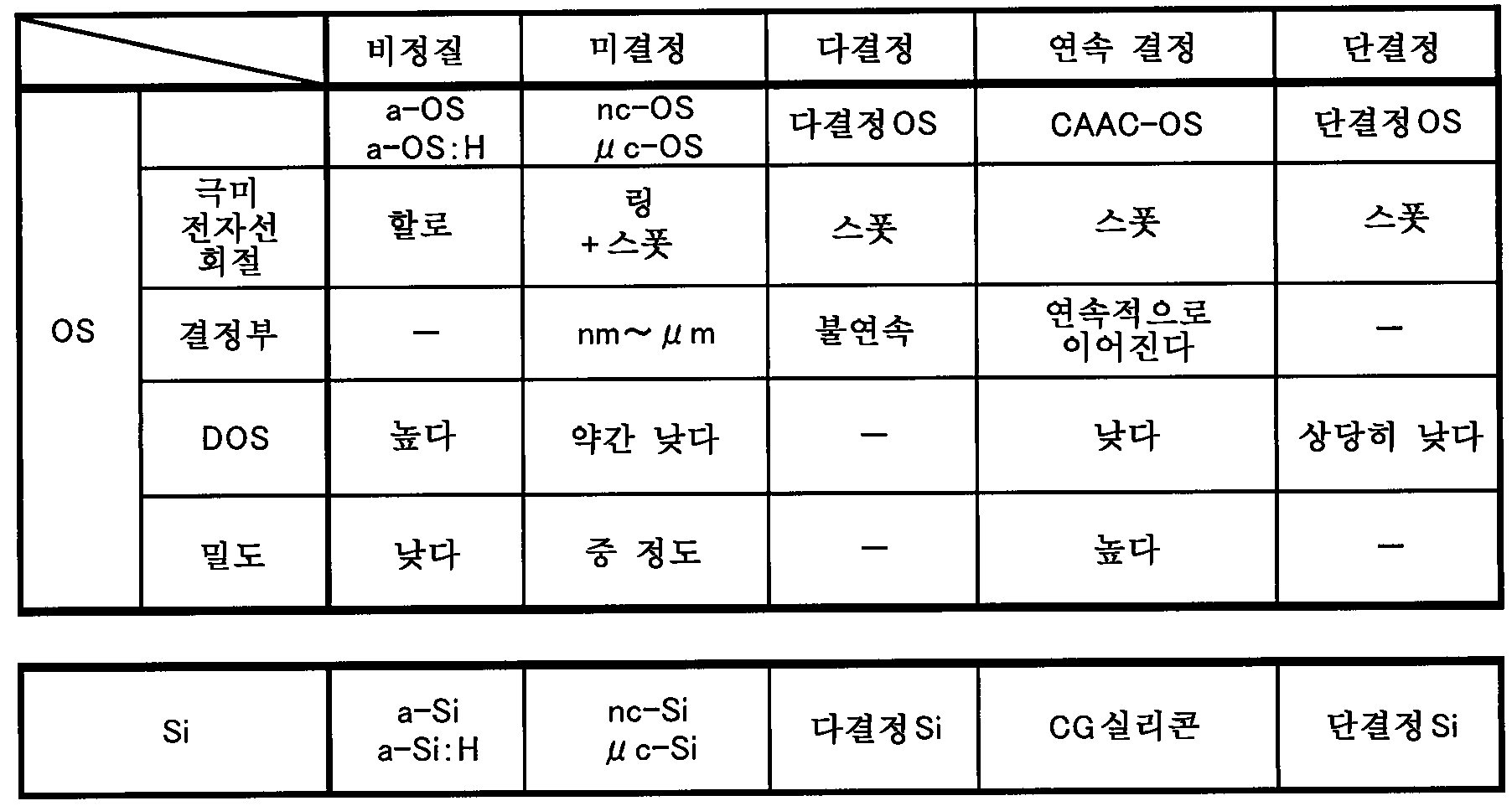
산화물 반도체의 결정 상태로는, 예를 들면, 표 1에 기재한 바와 같이 비정질 산화물 반도체(a-OS, a-OS: H), 미결정 산화물 반도체(nc-OS, μc-OS), 다결정 산화물 반도체(다결정 OS), 연속 결정 산화물 반도체(CAAC-OS), 단결정 산화물 반도체(단결정 OS) 등이 있다. 또한, 실리콘의 결정 상태로는, 예를 들면, 표 1에 기재한 바와 같이 비정질 실리콘(a-Si나 a-Si: H), 미결정 실리콘(nc-Si, μc-Si), 다결정 실리콘(다결정 Si), 연속 결정 실리콘(CG(Continuous Grain) 실리콘), 단결정 실리콘(단결정 Si) 등이 있다.As for the crystal state of oxide semiconductors, there are, for example, amorphous oxide semiconductor (a-OS, a-OS: H), microcrystalline oxide semiconductor (nc-OS, μc-OS), polycrystalline oxide semiconductor (polycrystalline OS), continuous crystal oxide semiconductor (CAAC-OS), single crystal oxide semiconductor (single crystal OS), etc., as shown in Table 1. In addition, as for the crystal state of silicon, there are, for example, amorphous silicon (a-Si or a-Si: H), microcrystalline silicon (nc-Si, μc-Si), polycrystalline silicon (polycrystalline Si), continuous crystal silicon (CG (Continuous Grain) silicon), single crystal silicon (single crystal Si), etc., as shown in Table 1.
각 결정 상태에서의 산화물 반도체에 대하여, 빔 직경을 10nmφ 이하로 결속시킨 전자선을 사용한 전자선 회절(극미 전자선 회절)을 행하면, 이하와 같은 전자선 회절 패턴(극미 전자선 회절 패턴)이 관측된다. 비정질 산화물 반도체에서는 할로 패턴(할로-링 또는 할로라고도 한다)이 관측된다. 미결정 산화물 반도체에서는 스폿 또는/및 링 패턴이 관측된다. 다결정 산화물 반도체에서는 스폿이 관측된다. 연속 결정 산화물 반도체에서는 스폿이 관측된다. 단결정 산화물 반도체에서는 스폿이 관측된다.When electron diffraction (micro electron diffraction) is performed using an electron beam focused to a beam diameter of 10 nmφ or less for an oxide semiconductor in each crystal state, the following electron diffraction patterns (micro electron diffraction patterns) are observed. In an amorphous oxide semiconductor, a halo pattern (also called a halo-ring or halo) is observed. In a microcrystalline oxide semiconductor, a spot or/and ring pattern is observed. In a polycrystalline oxide semiconductor, spots are observed. In a continuous crystal oxide semiconductor, spots are observed. In a single crystal oxide semiconductor, spots are observed.
또한, 극미 전자선 회절 패턴에서, 미결정 산화물 반도체는 결정부가 나노미터(nm)에서 마이크로미터(㎛)의 직경인 것을 알 수 있다. 다결정 산화물 반도체는 결정부와 결정부 사이에 입계를 갖고, 경계가 불연속인 것을 알 수 있다. 연속 결정 산화물 반도체는 결정부와 결정부 사이에 경계가 관측되지 않고, 연속적으로 이어지는 것을 알 수 있다.In addition, from the ultra-fine electron diffraction pattern, it can be seen that the microcrystalline oxide semiconductor has a crystal part with a diameter of nanometers (nm) to micrometers (㎛). It can be seen that the polycrystalline oxide semiconductor has grain boundaries between crystal parts, and that the boundaries are discontinuous. It can be seen that the continuous crystal oxide semiconductor has no boundaries observed between crystal parts, and that the crystal parts are continuously connected.
각 결정 상태에서의 산화물 반도체의 밀도에 대하여 설명한다. 비정질 산화물 반도체의 밀도는 낮다. 미결정 산화물 반도체의 밀도는 중 정도이다. 연속 결정 산화물 반도체의 밀도는 높다. 즉, 연속 결정 산화물 반도체의 밀도는 미결정 산화물 반도체의 밀도보다 높고, 미결정 산화물 반도체의 밀도는 비정질 산화물 반도체의 밀도보다 높다.The density of oxide semiconductors in each crystal state is explained. The density of amorphous oxide semiconductors is low. The density of microcrystalline oxide semiconductors is medium. The density of continuous crystalline oxide semiconductors is high. That is, the density of continuous crystalline oxide semiconductors is higher than that of microcrystalline oxide semiconductors, and the density of microcrystalline oxide semiconductors is higher than that of amorphous oxide semiconductors.
각 결정 상태에서의 산화물 반도체에 존재하는 상태 밀도(DOS)의 특징을 설명한다. 비정질 산화물 반도체는 DOS가 높다. 미결정 산화물 반도체는 DOS가 약간 낮다. 연속 결정 산화물 반도체는 DOS가 낮다. 단결정 산화물 반도체는 DOS가 상당히 낮다. 즉, 단결정 산화물 반도체는 연속 결정 산화물 반도체보다 DOS가 낮고, 연속 결정 산화물 반도체는 미결정 산화물 반도체보다 DOS가 낮고, 미결정 산화물 반도체는 비정질 산화물 반도체보다 DOS가 낮다.Describes the characteristics of the density of states (DOS) existing in oxide semiconductors in each crystal state. Amorphous oxide semiconductors have high DOS. Microcrystalline oxide semiconductors have slightly lower DOS. Continuous crystalline oxide semiconductors have low DOS. Single-crystal oxide semiconductors have considerably lower DOS. That is, single-crystal oxide semiconductors have lower DOS than continuous crystalline oxide semiconductors, continuous crystalline oxide semiconductors have lower DOS than microcrystalline oxide semiconductors, and microcrystalline oxide semiconductors have lower DOS than amorphous oxide semiconductors.
또한, 산화물 반도체막은 복수의 산화물 반도체막이 적층된 구조라도 좋다. 예를 들면, 도 9a에 도시한 트랜지스터와 같이, 반도체막을 제 1 산화물 반도체막(188a)과 제 2 산화물 반도체막(188b)의 적층으로 할 수 있다. 제 1 산화물 반도체막(188a)과 제 2 산화물 반도체막(188b)에 상이한 원자수 비의 금속 산화물을 사용하여도 좋다. 예를 들면, 한쪽의 산화물 반도체막에 2종류의 금속을 포함하는 산화물, 3종류의 금속을 포함하는 산화물, 4종류의 금속을 포함하는 산화물 중 하나를 사용하고, 다른 한쪽의 산화물 반도체막에 한쪽의 산화물 반도체막과 상이한 2종류의 금속을 포함하는 산화물, 3종류의 금속을 포함하는 산화물, 4종류의 금속을 포함하는 산화물을 사용하여도 좋다.In addition, the oxide semiconductor film may have a structure in which a plurality of oxide semiconductor films are laminated. For example, as in the transistor illustrated in Fig. 9a, the semiconductor film may be a laminate of a first oxide semiconductor film (188a) and a second oxide semiconductor film (188b). Metal oxides having different atomic ratios may be used for the first oxide semiconductor film (188a) and the second oxide semiconductor film (188b). For example, one of an oxide containing two types of metals, an oxide containing three types of metals, and an oxide containing four types of metals may be used for one oxide semiconductor film, and the other oxide semiconductor film may be used with an oxide containing two types of metals, an oxide containing three types of metals, or an oxide containing four types of metals that are different from those of the one oxide semiconductor film.
또한, 제 1 산화물 반도체막(188a)과 제 2 산화물 반도체막(188b)의 구성 원소를 동일하게 하고, 양자의 원자수 비를 상이하게 하여도 좋다. 예를 들면, 한쪽의 산화물 반도체막의 원자수 비를 In:Ga:Zn=3:1:2로 하고, 다른 한쪽의 산화물 반도체막의 원자수 비를 In:Ga:Zn=1:1:1로 하여도 좋다. 또한, 한쪽의 산화물 반도체막의 원자수 비를 In:Ga:Zn=2:1:3으로 하고, 다른 한쪽의 산화물 반도체막의 원자수 비를 In:Ga:Zn=1:3:2로 하여도 좋다. 또한, 한쪽의 산화물 반도체막의 원자수 비를 In:Ga:Zn=1:1:1로 하고, 다른 한쪽의 산화물 반도체막의 원자수 비를 In:Ga:Zn=1:3:2로 하여도 좋다. 또한, 한쪽의 산화물 반도체막의 원자수 비를 In:Ga:Zn=1:1:1로 하고, 다른 한쪽의 산화물 반도체막의 원자수 비를 In:Ga:Zn=1:6:4로 하여도 좋다. 또한, 한쪽의 산화물 반도체막의 원자수 비를 In:Ga:Zn=1:1:1로 하고, 다른 한쪽의 산화물 반도체막의 원자수 비를 In:Ga:Zn=1:9:6으로 하여도 좋다. 또한, 각 산화물 반도체막의 원자수 비는 오차로서 상기의 원자수 비의 ±20%의 변동을 포함한다.In addition, the constituent elements of the first oxide semiconductor film (188a) and the second oxide semiconductor film (188b) may be the same, and their atomic ratios may be different. For example, the atomic ratio of one oxide semiconductor film may be In:Ga:Zn=3:1:2, and the atomic ratio of the other oxide semiconductor film may be In:Ga:Zn=1:1:1. In addition, the atomic ratio of one oxide semiconductor film may be In:Ga:Zn=2:1:3, and the atomic ratio of the other oxide semiconductor film may be In:Ga:Zn=1:3:2. In addition, the atomic ratio of one oxide semiconductor film may be In:Ga:Zn=1:1:1, and the atomic ratio of the other oxide semiconductor film may be In:Ga:Zn=1:3:2. In addition, the atomic ratio of one oxide semiconductor film may be In:Ga:Zn=1:1:1, and the atomic ratio of the other oxide semiconductor film may be In:Ga:Zn=1:6:4. In addition, the atomic ratio of one oxide semiconductor film may be In:Ga:Zn=1:1:1, and the atomic ratio of the other oxide semiconductor film may be In:Ga:Zn=1:9:6. In addition, the atomic ratio of each oxide semiconductor film includes a variation of ±20% of the above atomic ratio as an error.
이때, 한쪽의 산화물 반도체막과 다른 한쪽의 산화물 반도체막 중, 게이트 전극에 가까운 측(채널측)의 산화물 반도체막의 In과 Ga의 원자수 비를 In≥Ga로 하고, 게이트 전극에서 먼 측(백 채널측)의 산화물 반도체막의 In과 Ga의 원자수 비를 In<Ga로 함으로써 전계 효과 이동도가 높은 트랜지스터를 제작할 수 있다. 한편, 채널측의 산화물 반도체막의 In과 Ga의 원자수 비를 In<Ga로 하고, 백 채널측의 산화물 반도체막의 In과 Ga의 원자수 비를 In≥Ga로 함으로써, 트랜지스터의 경시 변화나 신뢰성 시험에 의한 임계값 전압의 변동량을 저감시킬 수 있다.At this time, by setting the atomic ratio of In and Ga in the oxide semiconductor film on the side near the gate electrode (channel side) among the oxide semiconductor films on one side and the oxide semiconductor film on the other side to In≥Ga and setting the atomic ratio of In and Ga in the oxide semiconductor film on the side far from the gate electrode (back-channel side) to In<Ga, a transistor having high field-effect mobility can be manufactured. On the other hand, by setting the atomic ratio of In and Ga in the oxide semiconductor film on the channel side to In<Ga and setting the atomic ratio of In and Ga in the oxide semiconductor film on the back-channel side to In≥Ga, it is possible to reduce the amount of variation in threshold voltage due to change over time or reliability test of the transistor.
또한, 트랜지스터의 반도체막을 제 1 산화물 반도체막 내지 제 3 산화물 반도체막으로 이루어지는 3층 구조로 하여도 좋다. 이때, 제 1 산화물 반도체막 내지 제 3 산화물 반도체막의 구성 원소를 동일하게 하고, 또한 각각의 원자수 비를 상이하게 하여도 좋다. 반도체막을 3층 구조로 하는 트랜지스터의 구성에 대하여 도 9b를 사용하여 설명한다.In addition, the semiconductor film of the transistor may be formed into a three-layer structure composed of a first oxide semiconductor film to a third oxide semiconductor film. At this time, the constituent elements of the first oxide semiconductor film to the third oxide semiconductor film may be the same, and further, the atomic ratios of each may be different. The configuration of a transistor having a three-layer semiconductor film structure will be described using Fig. 9b.
도 9b에 도시한 트랜지스터는 제 1 산화물 반도체막(199a), 제 2 산화물 반도체막(199b), 및 제 3 산화물 반도체막(199c)이 게이트 절연막(127)측에서 순차적으로 적층되어 있다. 제 1 산화물 반도체막(199a) 및 제 3 산화물 반도체막(199c)을 구성하는 재료는, InM1xZnyOz(x≥1, y>1, z>0, M1=Ga, Hf 등)로 표기할 수 있는 재료를 사용한다. 다만, 제 1 산화물 반도체막(199a) 및 제 3 산화물 반도체막(199c)을 구성하는 재료에 Ga를 포함시킬 경우, 포함시키는 Ga의 비율이 많은, 구체적으로는 InM1XZnYOZ로 표기할 수 있는 재료로 X=10을 초과하면 성막시에 가루가 발생할 우려가 있어, 부적합하다.In the transistor illustrated in Fig. 9b, a first oxide semiconductor film (199a), a second oxide semiconductor film (199b), and a third oxide semiconductor film (199c) are sequentially laminated on the gate insulating film (127) side. The material constituting the first oxide semiconductor film (199a) and the third oxide semiconductor film (199c) uses a material that can be expressed as InM 1x Zn y O z (x ≥ 1, y > 1, z > 0, M 1 = Ga, Hf, etc.). However, when Ga is included in the material constituting the first oxide semiconductor film (199a) and the third oxide semiconductor film (199c), if the proportion of Ga included is large, specifically, if it exceeds X = 10 with a material that can be expressed as InM 1X Zn Y O Z, there is a concern that powder may be generated during film formation, and thus it is not suitable.
또한, 제 2 산화물 반도체막(199b)을 구성하는 재료는 InM2xZnyOz(x≥1, y≥x, z>0, M2=Ga, Sn 등)로 표기할 수 있는 재료를 사용한다.In addition, the material constituting the second oxide semiconductor film (199b) uses a material that can be expressed as InM 2x Zn y O z (x≥1, y≥x, z>0, M 2 =Ga, Sn, etc.).
제 1 산화물 반도체막(199a)의 전도대 하단 및 제 3 산화물 반도체막(199c)의 전도대 하단에 비하여 제 2 산화물 반도체막(199b)의 전도대 하단이 진공 준위에서 가장 깊어지는 우물형 구조를 구성하도록 제 1, 제 2 및 제 3 산화물 반도체막의 재료를 적절히 선택한다.The materials of the first, second, and third oxide semiconductor films are appropriately selected so as to form a well-shaped structure in which the bottom of the conduction band of the second oxide semiconductor film (199b) becomes deepest at the vacuum level compared to the bottom of the conduction band of the first oxide semiconductor film (199a) and the bottom of the conduction band of the third oxide semiconductor film (199c).
또한, 산화물 반도체막에 있어서 제 14족 원소의 하나인 실리콘이나 탄소는 도너 준위의 형성에 기여하는 경우가 있다. 이 때문에, 실리콘이나 탄소가 산화물 반도체막에 포함되면 산화물 반도체막은 n형화되어 버린다. 따라서, 실리콘 및 탄소 각각의 농도는 3×10¹⁸/cm3 이하, 바람직하게는 3×10¹⁷/cm3로 하는 영역을 갖도록 각 산화물 반도체막을 형성하는 것이 바람직하다. 특히, 제 2 산화물 반도체막(199b)에 제 14족 원소가 많이 혼입되지 않도록, 제 1 산화물 반도체막(199a) 및 제 3 산화물 반도체막(199c)으로, 캐리어 패스가 되는 제 2 산화물 반도체막(199b)을 끼우는, 또는 둘러싸는 구성으로 하는 것이 바람직하다. 즉, 제 1 산화물 반도체막(199a) 및 제 3 산화물 반도체막(199c)은 실리콘, 탄소 등의 제 14족 원소가 제 2 산화물 반도체막 199b에 혼입되는 것을 방지하는 배리어막이라고도 할 수 있다.In addition, in the oxide semiconductor film, silicon or carbon, which are elements of Group 14, sometimes contribute to the formation of a donor level. For this reason, if silicon or carbon is included in the oxide semiconductor film, the oxide semiconductor film becomes n-type. Therefore, it is preferable to form each oxide semiconductor film so that the concentration of silicon and carbon, respectively, has a region of 3×10 18 /cm 3 or less, preferably 3×10 17 /cm 3 . In particular, in order to prevent a large amount of Group 14 elements from being mixed into the second oxide semiconductor film (199b), it is preferable to have a configuration in which the second oxide semiconductor film (199b), which serves as a carrier path, is sandwiched or surrounded by the first oxide semiconductor film (199a) and the third oxide semiconductor film (199c). That is, the first oxide semiconductor film (199a) and the third oxide semiconductor film (199c) can also be said to be barrier films that prevent group 14 elements such as silicon and carbon from being mixed into the second
예를 들면, 제 1 산화물 반도체막(199a) 및 제 3 산화물 반도체막(199c)을 원자수 비가 In:Ga:Zn=1:3:2, 또는 1:6:4, 또는 1:9:6인 산화물 반도체막으로 형성하고, 제 2 산화물 반도체막(199b)의 원자수 비가 In:Ga:Zn=1:1:1, 또는 3:1:2인 산화물 반도체막으로 형성할 수 있다.For example, the first oxide semiconductor film (199a) and the third oxide semiconductor film (199c) can be formed as oxide semiconductor films having an atomic ratio of In:Ga:Zn=1:3:2, or 1:6:4, or 1:9:6, and the second oxide semiconductor film (199b) can be formed as an oxide semiconductor film having an atomic ratio of In:Ga:Zn=1:1:1, or 3:1:2.
또는, 제 1 산화물 반도체막(199a)을 원자수 비가 In:Ga:Zn=1:3:2인 산화물 반도체막으로 형성하고, 제 2 산화물 반도체막(199b)을 원자수 비가 In:Ga:Zn=1:1:1 또는 In:Ga:Zn=3:1:2인 산화물 반도체막으로 형성하고, 제 3 산화물 반도체막(199c)을 원자수 비가 In:Ga:Zn=1:6:4, 또는 1:9:6인 산화물 반도체막으로 형성하여도 좋다.Alternatively, the first oxide semiconductor film (199a) may be formed as an oxide semiconductor film having an atomic ratio of In:Ga:Zn=1:3:2, the second oxide semiconductor film (199b) may be formed as an oxide semiconductor film having an atomic ratio of In:Ga:Zn=1:1:1 or In:Ga:Zn=3:1:2, and the third oxide semiconductor film (199c) may be formed as an oxide semiconductor film having an atomic ratio of In:Ga:Zn=1:6:4 or 1:9:6.
제 1 산화물 반도체막(199a) 내지 제 3 산화물 반도체막(199c)의 구성 원소는 동일하므로, 제 2 산화물 반도체막(199b)은 제 1 산화물 반도체막(199a)과의 계면에서의 결함 준위(트랩 준위)가 적다. 상세하게는, 상기 결함 준위(트랩 준위)는, 게이트 절연막(127)과 제 1 산화물 반도체막(199a)의 계면에서의 결함 준위보다도 적다. 이 때문에, 상기한 바와 같이 산화물 반도체막이 적층되어 있음으로써 트랜지스터의 경시 변화나 신뢰성 시험에 의한 임계값 전압의 변동량을 저감시킬 수 있다.Since the constituent elements of the first oxide semiconductor film (199a) to the third oxide semiconductor film (199c) are the same, the second oxide semiconductor film (199b) has fewer defect levels (trap levels) at the interface with the first oxide semiconductor film (199a). Specifically, the defect levels (trap levels) are smaller than the defect levels at the interface between the gate insulating film (127) and the first oxide semiconductor film (199a). Therefore, by stacking the oxide semiconductor films as described above, it is possible to reduce the amount of variation in threshold voltage due to changes over time in the transistor or reliability tests.
또한, 제 1 산화물 반도체막(199a)의 전도대 하단 및 제 3 산화물 반도체막(199c)의 전도대 하단에 비하여 제 2 산화물 반도체막(199b)의 전도대 하단이 진공 준위에서 가장 깊어지는 우물형 구조를 구성하도록, 제 1, 제 2 및 제 3 산화물 반도체막의 재료를 적절히 선택함으로써, 트랜지스터의 전계 효과 이동도를 높이는 것이 가능함과 동시에 트랜지스터의 경시 변화나 신뢰성 시험에 의한 임계값 전압의 변동량을 저감시킬 수 있다.In addition, by appropriately selecting the materials of the first, second and third oxide semiconductor films so that a well-shaped structure is formed in which the lower end of the conduction band of the second oxide semiconductor film (199b) becomes deepest in the vacuum level compared to the lower end of the conduction band of the first oxide semiconductor film (199a) and the lower end of the conduction band of the third oxide semiconductor film (199c), it is possible to increase the field effect mobility of the transistor, while reducing the amount of change in threshold voltage due to changes in the transistor over time or reliability tests.
또한, 제 1 산화물 반도체막(199a) 내지 제 3 산화물 반도체막(199c)에, 결정성이 상이한 산화물 반도체를 적용하여도 좋다. 즉, 단결정 산화물 반도체, 다결정 산화물 반도체, 미결정(나노 결정) 산화물 반도체, 비정질 산화물 반도체, 및 CAAC-OS막을 적절히 조합한 구성으로 하여도 좋다. 또한, 제 1 산화물 반도체막(199a) 내지 제 3 산화물 반도체막(199c) 중 어느 하나에 비정질 산화물 반도체를 적용하면, 산화물 반도체막의 내부 응력이나 외부로부터의 응력을 완화시키고, 트랜지스터의 특성 편차가 저감되며, 또한 트랜지스터의 경시 변화나 신뢰성 시험에 의한 임계값 전압의 변동량을 저감시킬 수 있다.In addition, oxide semiconductors having different crystallinities may be applied to the first oxide semiconductor film (199a) to the third oxide semiconductor film (199c). That is, a configuration in which a single-crystal oxide semiconductor, a polycrystalline oxide semiconductor, a microcrystalline (nano-crystal) oxide semiconductor, an amorphous oxide semiconductor, and a CAAC-OS film are appropriately combined may be used. In addition, when an amorphous oxide semiconductor is applied to any one of the first oxide semiconductor film (199a) to the third oxide semiconductor film (199c), internal stress or external stress of the oxide semiconductor film is alleviated, characteristic deviation of the transistor is reduced, and also variation in threshold voltage due to change over time of the transistor or reliability test can be reduced.
또한, 적어도 채널 형성 영역이 될 수 있는 제 2 산화물 반도체막(199b)은 CAAC-OS막인 것이 바람직하다.Additionally, it is preferable that at least the second oxide semiconductor film (199b) that can become a channel forming region is a CAAC-OS film.
또한, 산소와 결합하기 쉬운 도전 재료(예를 들면, 소스 전극 또는 드레인 전극에 사용되는 금속)와 산화물 반도체막을 접촉시키면, 산화물 반도체막 중의 산소가 산소와 결합하기 쉬운 도전 재료측으로 확산하는 현상이 일어난다. 상기 현상은 온도가 높을수록 현저하게 일어난다. 트랜지스터의 제작 공정에는 몇 가지 가열 공정이 있기 때문에, 상기 현상에 의해, 산화물 반도체층의 소스 전극 또는 드레인 전극과 접촉한 근방의 영역에 산소 결손이 발생하고, 상기 영역은 n형화된다. 따라서, n형화된 상기 영역은 트랜지스터의 소스 또는 드레인으로서 작용시킬 수 있다.In addition, when a conductive material that easily bonds with oxygen (for example, a metal used for a source electrode or a drain electrode) is brought into contact with an oxide semiconductor film, a phenomenon occurs in which oxygen in the oxide semiconductor film diffuses toward the conductive material that easily bonds with oxygen. This phenomenon occurs more significantly as the temperature increases. Since there are several heating processes in the transistor manufacturing process, due to the above phenomenon, oxygen vacancies occur in a region near the oxide semiconductor layer in contact with the source electrode or the drain electrode, and the region becomes n-type. Therefore, the region that becomes n-type can function as a source or drain of the transistor.
상기 n형화된 영역은 도 9a, 도 9b에 예시된다. 반도체막 중에 점선으로 표시되는 경계(135)는 진성 반도체 영역과 n형 반도체 영역의 경계이고, 산화물 반도체에서의 소스 전극 또는 드레인 전극과 접촉한 근방의 영역이 n형화된 영역이 된다. 또한, 경계(135)는 모식적으로 나타난 것이고, 실제로는 명료하지 않는 경우가 있다. 또한, 경계(135)의 위치도 도시한 위치와는 다른 경우가 있다.The above n-type region is exemplified in Fig. 9a and Fig. 9b. The boundary (135) indicated by a dotted line in the semiconductor film is the boundary between the intrinsic semiconductor region and the n-type semiconductor region, and the region near the source electrode or drain electrode in the oxide semiconductor becomes the n-type region. In addition, the boundary (135) is shown schematically, and in reality, it may not be clear in some cases. In addition, the position of the boundary (135) may also be different from the position shown.
또한, 본 실시형태는, 본 명세서에서 나타내는 다른 실시형태와 적절히 조합할 수 있다.In addition, this embodiment can be appropriately combined with other embodiments described in this specification.
(실시형태 3)(Embodiment 3)
본 실시형태에서는, 본 발명의 일 양태에 사용할 수 있는 나노 결정 산화물 반도체막의 전자선 회절 패턴, 및 국재(局在) 준위로 설명한다.In this embodiment, the electron diffraction pattern and local state of a nanocrystal oxide semiconductor film that can be used in one aspect of the present invention are described.
나노 결정 산화물 반도체막은, 빔 직경이 10nmφ 이하로 한 전자선 회절(극미 전자선 회절)을 사용한 전자선 회절 패턴에 있어서, 비정질 상태를 나타내는 할로 패턴과도 상이하고, 특정한 면에 배향한 결정 상태를 나타내는 규칙성을 갖는 스폿과도 상이하며, 방향성을 갖지 않는 스폿이 관찰되는 산화물 반도체막이다.A nanocrystal oxide semiconductor film is an oxide semiconductor film in which, in an electron diffraction pattern using electron diffraction (ultra-fine electron diffraction) with a beam diameter of 10 nmφ or less, a halo pattern indicating an amorphous state is observed, spots having no directionality are observed, and spots having regularity indicating a crystalline state oriented in a specific plane are observed.
도 13a에 나노 결정 산화물 반도체막의 단면 TEM(Transmission Electron Microscopy(투과형 전자 현미경)) 상을 도시한다. 또한, 도 13b에 도 13a의 포인트(1)에서 극미 전자선 회절을 사용하여 측정한 전자선 회절 패턴을, 도 13c에 도 13a의 포인트(2)에서 극미 전자선 회절을 사용하여 측정한 전자선 회절 패턴을, 도 13d에 도 13a의 포인트(3)에서 극미 전자선 회절을 사용하여 측정한 전자선 회절 패턴을 각각 도시한다.Fig. 13a shows a cross-sectional TEM (Transmission Electron Microscopy) image of a nanocrystal oxide semiconductor film. In addition, Fig. 13b shows an electron diffraction pattern measured using ultra-small electron diffraction at point (1) of Fig. 13a, Fig. 13c shows an electron diffraction pattern measured using ultra-small electron diffraction at point (2) of Fig. 13a, and Fig. 13d shows an electron diffraction pattern measured using ultra-small electron diffraction at point (3) of Fig. 13a.
도 13a 내지 도 13d에서는, 나노 결정 산화물 반도체막의 일례로서, In-Ga-Zn계 산화물막을 석영 유리 기판 위에 막 두께 50nm로 성막한 시료를 사용한다. 도 13a 내지 도 13d에 도시한 나노 결정 산화물 반도체막의 성막 조건은, In:Ga:Zn=1:1:1(원자수 비)인 산화물 타깃을 사용하고, 산소 분위기하(유량 45sccm), 압력 0.4Pa, 직류(DC) 전원 0.5kW, 기판 온도를 실온으로 하였다. 그리고, 성막한 나노 결정 산화물 반도체막을 100nm 이하(예를 들면, 40nm±10nm)의 폭으로 박편화하여, 단면 TEM상 및 극미 전자선 회절에 의한 전자선 회절 패턴을 얻었다.In Figs. 13a to 13d, as an example of a nano-crystal oxide semiconductor film, a sample in which an In-Ga-Zn-based oxide film is deposited on a quartz glass substrate with a film thickness of 50 nm is used. The deposition conditions of the nano-crystal oxide semiconductor film illustrated in Figs. 13a to 13d are as follows: an oxide target of In:Ga:Zn = 1:1:1 (atomic ratio) was used, an oxygen atmosphere (flow
도 13a는, 투과형 전자 현미경(히타치하이테크놀러지즈 제조 「H-9000NAR」)을 사용하고, 가속 전압을 300kV, 배율 200만배로 하여 촬영한 나노 결정 산화물 반도체막의 단면 TEM상이다. 또한, 도 13b 내지 도 13d는, 투과형 전자 현미경(히타치하이테크놀러지즈 제조 「HF-2000」)을 사용하고, 가속 전압을 200kV, 빔 직경을 약 1nmφ로 하여 극미 전자선 회절에 의해 얻어진 전자선 회절 패턴이다. 또한, 빔 직경을 약 1nmφ로 하였을 경우의 극미 전자선 회절에서의 측정 범위는 5nmφ 이상 10nmφ 이하이다.Fig. 13a is a cross-sectional TEM image of a nanocrystal oxide semiconductor film, photographed using a transmission electron microscope ("H-9000NAR" manufactured by Hitachi High-Technologies, Inc.) at an acceleration voltage of 300 kV and a magnification of 2,000,000 times. In addition, Figs. 13b to 13d are electron diffraction patterns obtained by microscopic electron diffraction using a transmission electron microscope ("HF-2000" manufactured by Hitachi High-Technologies, Inc.) at an acceleration voltage of 200 kV and a beam diameter of about 1 nmφ. In addition, the measurement range in microscopic electron diffraction when the beam diameter is about 1 nmφ is 5 nmφ or more and 10 nmφ or less.
도 13b에 도시한 바와 같이 나노 결정 산화물 반도체막은, 극미 전자선 회절을 사용한 전자선 회절 패턴에 있어서, 원주 형상으로 배치된 복수의 스폿(휘점)이 관찰된다. 바꾸어 말하면, 나노 결정 산화물 반도체막에서는, 원주 형상(동심원 형상)으로 분포된 복수의 스폿이 관찰된다고도 할 수 있다. 또는, 원주 형상으로 분포된 복수의 스폿이 복수의 동심원을 형성한다고도 할 수 있다.As illustrated in Fig. 13b, in the electron diffraction pattern using ultra-fine electron diffraction, a nano-crystal oxide semiconductor film is observed to have a plurality of spots (bright spots) arranged in a circular shape. In other words, it can be said that a plurality of spots distributed in a circular shape (concentric circle shape) are observed in the nano-crystal oxide semiconductor film. Alternatively, it can be said that a plurality of spots distributed in a circular shape form a plurality of concentric circles.
또한, 석영 유리 기판과의 계면 근방인 도 13d 및, 나노 결정 산화물 반도체막의 막 두께 방향 중앙부의 도 13c에서도 도 13b와 같이 원주 형상으로 분포된 복수의 스폿이 관찰된다. 도 13c에서, 메인 스폿에서 원주 형상의 스폿까지의 거리는 3.88/nm에서 4.93/nm이었다. 면 간격으로 환산하면, 0.203nm에서 0.257nm이다.In addition, multiple spots distributed in a cylindrical shape, as in Fig. 13b, are observed in Fig. 13d near the interface with the quartz glass substrate and in Fig. 13c at the center of the film thickness direction of the nano-crystal oxide semiconductor film. In Fig. 13c, the distance from the main spot to the cylindrical spot was 3.88/nm to 4.93/nm. Converted to the inter-surface spacing, it is 0.203 nm to 0.257 nm.
도 13a 내지 도 13d의 극미 전자선 회절 패턴으로부터, 나노 결정 산화물 반도체막은 면 방위가 불규칙하고 또한 크기가 다른 결정부가 복수 혼재하는 막인 것을 알 수 있다.From the ultra-fine electron diffraction patterns of FIGS. 13a to 13d, it can be seen that the nano-crystal oxide semiconductor film is a film in which multiple crystal parts having irregular plane orientations and different sizes coexist.
이어서, 도 14a에 나노 결정 산화물 반도체막의 평면 TEM상을 도시한다. 또한, 도 14b에 도 14a에서 원으로 둘러싼 영역을 제한 시야 전자선 회절을 사용하여 측정한 전자선 회절 패턴을 도시한다.Next, Fig. 14a shows a planar TEM image of a nanocrystal oxide semiconductor film. In addition, Fig. 14b shows an electron diffraction pattern measured using limited field electron diffraction of the area circled in Fig. 14a.
도 14a 및 도 14b에서는, 나노 결정 산화물 반도체막의 일례로서, In-Ga-Zn계 산화물막을 석영 유리 기판 위에 막 두께 30nm로 성막한 시료를 사용한다. 도 14a 및 도 14b에 도시한 나노 결정 산화물 반도체막의 성막 조건은 In:Ga:Zn=1:1:1(원자수 비)인 산화물 타깃을 사용하고, 산소 분위기하(유량 45sccm), 압력 0.4Pa, 직류(DC) 전원 0.5kW, 기판 온도를 실온으로 하였다. 그리고, 시료를 박편화하여, 나노 결정 산화물 반도체막의 나노 결정 산화물 반도체막의 평면 TEM상 및 전자선 회절에 의한 전자선 회절 패턴을 얻었다.In Figs. 14a and 14b, as an example of a nano-crystal oxide semiconductor film, a sample in which an In-Ga-Zn-based oxide film is deposited on a quartz glass substrate with a film thickness of 30 nm is used. The deposition conditions of the nano-crystal oxide semiconductor film illustrated in Figs. 14a and 14b are as follows: an oxide target of In:Ga:Zn = 1:1:1 (atomic ratio), an oxygen atmosphere (flow
도 14a는, 투과형 전자 현미경(히타치하이테크놀러지즈 제조 「H-9000NAR」)을 사용하고, 가속 전압을 300kV, 배율 50만배로 하여 촬영한 나노 결정 산화물 반도체막의 평면 TEM 사진이다. 또한, 도 14b는, 제한 시야를 300nmφ로 하여 전자선 회절에 의해 얻어진 전자선 회절 패턴이다. 또한, 전자선의 확대를 고려하면, 측정 범위는 300nmφ 이상이다.Fig. 14a is a planar TEM image of a nanocrystal oxide semiconductor film taken using a transmission electron microscope (H-9000NAR manufactured by Hitachi High-Technologies) at an acceleration voltage of 300 kV and a magnification of 500,000 times. In addition, Fig. 14b is an electron diffraction pattern obtained by electron diffraction with a limited field of view of 300 nmφ. In addition, considering the magnification of the electron beam, the measurement range is 300 nmφ or more.
도 14b에 도시한 바와 같이 나노 결정 산화물 반도체막은, 극미 전자선 회절보다도 측정 범위가 넓은 제한 시야 전자선 회절을 사용한 전자선 회절 패턴에서는, 극미 전자선 회절에 의해 관찰된 복수의 스폿이 보이지 않고, 할로 패턴이 관찰된다.As illustrated in Fig. 14b, in the electron diffraction pattern using limited-field electron diffraction, which has a wider measurement range than ultra-small electron diffraction, the nano-crystal oxide semiconductor film does not show multiple spots observed by ultra-small electron diffraction, but instead, a halo pattern is observed.
다음에, 도 15a 내지 도 15c에, 도 13a 내지 도 13d 및 도 14a 및 도 14b의 전자선 회절 패턴에서의 회절 강도의 분포를 개념적으로 도시한다. 도 15a는, 도 13b 내지 도 13d에 도시한 극미 전자선 회절 패턴에서의 회절 강도의 분포의 개념도이다. 또한, 도 15b는, 도 14b에 도시한 제한 시야 전자선 회절 패턴에서의 회절 강도의 분포의 개념도이다. 또한, 도 15c는 단결정 구조 또는 다결정 구조의 전자선 회절 패턴에서의 회절 강도의 분포의 개념도이다.Next, Figs. 15a to 15c conceptually illustrate the distribution of diffraction intensities in the electron diffraction patterns of Figs. 13a to 13d and Figs. 14a and 14b. Fig. 15a is a conceptual diagram of the distribution of diffraction intensities in the ultra-fine electron diffraction patterns illustrated in Figs. 13b to 13d. In addition, Fig. 15b is a conceptual diagram of the distribution of diffraction intensities in the limited-field electron diffraction pattern illustrated in Fig. 14b. In addition, Fig. 15c is a conceptual diagram of the distribution of diffraction intensities in the electron diffraction pattern of a single crystal structure or a polycrystal structure.
도 15a 내지 도 15c에서, 세로축은 스폿 등의 분포를 나타내는 전자선 회절 강도(임의 단위), 가로축은 메인 스폿으로부터의 거리를 나타낸다.In Figures 15a to 15c, the vertical axis represents the electron diffraction intensity (arbitrary unit) showing the distribution of spots, etc., and the horizontal axis represents the distance from the main spot.
도 15c에 도시한 단결정 구조 또는 다결정 구조에서는, 결정부가 배향하는 면의 면 간격(d값)에 따른, 메인 스폿으로부터의 특정한 거리에 스폿이 관찰된다.In the single crystal structure or polycrystal structure illustrated in Fig. 15c, spots are observed at a specific distance from the main spot according to the spacing (d value) of the planes along which the crystal portions are oriented.
한편, 도 13a 내지 도 13d에 도시한 바와 같이 나노 결정 산화물 반도체막의 극미 전자선 회절 패턴에서 관찰되는 복수의 스폿에 의해 형성된 원주 형상의 영역은, 비교적 큰 폭을 갖는다. 따라서, 도 15a는 이산적(離散的)인 강도 분포를 나타낸다. 또한, 극미 전자선 회절 패턴에 있어서, 동심원 형상의 영역 사이에 명확한 스폿이 되지 않는 것의 휘도가 높은 영역이 존재하는 것을 알 수 있다.Meanwhile, as shown in FIGS. 13a to 13d, a cylindrical region formed by a plurality of spots observed in the microscopic electron diffraction pattern of the nano-crystal oxide semiconductor film has a relatively large width. Therefore, FIG. 15a shows a discrete intensity distribution. In addition, it can be seen that in the microscopic electron diffraction pattern, there exists a region of high brightness where no clear spot exists between the concentric circular regions.
또한, 도 15b에 도시한 바와 같이, 나노 결정 산화물 반도체막의 제한 시야 전자선 회절 패턴에서의 전자선 회절 강도 분포는, 연속적인 강도 분포를 나타낸다. 도 15b는, 도 15a에 도시한 전자선 회절 강도 분포를 광범위하게 관찰한 결과와 근사 가능하므로, 복수의 스폿이 중첩되어 이어져서, 연속적인 강도 분포가 얻어진 것이라고 고찰할 수 있다.In addition, as illustrated in Fig. 15b, the electron diffraction intensity distribution in the limited field electron diffraction pattern of the nano-crystal oxide semiconductor film shows a continuous intensity distribution. Since Fig. 15b can be approximated to the result of observing the electron diffraction intensity distribution shown in Fig. 15a over a wide area, it can be considered that a continuous intensity distribution is obtained by overlapping and connecting multiple spots.
도 15a 내지 도 15c에 도시한 바와 같이, 나노 결정 산화물 반도체막은, 면 방위가 불규칙하고 또한 크기가 다른 결정부가 복수 혼재하는 막이고, 또한, 그 결정부는, 제한 시야 전자선 회절 패턴에서는 스폿이 관찰되지 않는 정도로 극히 미세한 것이 시사된다.As illustrated in FIGS. 15A to 15C, the nanocrystal oxide semiconductor film is a film in which multiple crystal parts having irregular surface orientations and different sizes coexist, and furthermore, the crystal parts are so fine that no spots are observed in a limited field electron diffraction pattern.
복수의 스폿이 관찰된 도 13a 내지 도 13d에 있어서, 나노 결정 산화물 반도체막은 50nm 이하로 박편화되어 있다. 또한 전자선의 빔 직경은 1nmφ로 결속되어 있기 때문에, 그 측정 범위는 5nm 이상 10nm 이하이다. 따라서, 나노 결정 산화물 반도체막에 포함되는 결정부는 50nm 이하이고, 예를 들면, 10nm 이하 또는 5nm 이하인 것이 추측된다.In FIGS. 13A to 13D, where multiple spots are observed, the nano-crystal oxide semiconductor film is thinned to 50 nm or less. In addition, since the beam diameter of the electron beam is bound to 1 nmφ, the measurement range is 5 nm or more and 10 nm or less. Therefore, it is presumed that the crystal part included in the nano-crystal oxide semiconductor film is 50 nm or less, for example, 10 nm or less or 5 nm or less.
여기에서, 도 16에, 석영 유리 기판에서의 극미 전자선 회절 패턴을 도시한다. 측정 조건은 도 13b 내지 도 13d에 도시한 전자선 회절 패턴과 같게 하였다.Here, Fig. 16 shows an ultra-fine electron diffraction pattern on a quartz glass substrate. The measurement conditions were the same as those for the electron diffraction patterns shown in Figs. 13b to 13d.
도 16에 도시한 바와 같이, 비정질 구조를 갖는 석영 유리 기판에서는, 특정한 스폿을 갖지 않고, 메인 스폿에서 휘도가 연속적으로 변화되는 할로 패턴이 관측된다. 이렇게, 비정질 구조를 갖는 막에서는 극히 미소한 영역의 전자선 회절을 행하여도, 나노 결정 산화물 반도체막에서 관찰되는 바와 같은 원주 형상으로 분포된 복수의 스폿이 관찰되지 않는다. 따라서, 도 13b 내지 도 13d에서 관찰되는 원주 형상으로 분포된 복수의 스폿은, 나노 결정 산화물 반도체막에 특유한 것이라는 사실이 확인된다.As illustrated in Fig. 16, in a quartz glass substrate having an amorphous structure, a halo pattern is observed in which the brightness changes continuously from the main spot without a specific spot. In this way, in a film having an amorphous structure, even when electron beam diffraction is performed in an extremely small area, a plurality of spots distributed in a columnar shape as observed in a nano-crystal oxide semiconductor film is not observed. Therefore, it is confirmed that the plurality of spots distributed in a columnar shape observed in Figs. 13b to 13d are unique to a nano-crystal oxide semiconductor film.
또한, 도 17에, 도 13a에 도시한 포인트 2에 빔 직경을 약 1nmφ로 결속한 전자선을 1분간 조사한 후에, 측정한 전자선 회절 패턴을 도시한다.In addition, Fig. 17 shows an electron beam diffraction pattern measured after irradiating
도 17에 도시한 전자선 회절 패턴은, 도 13c에 도시한 전자선 회절 패턴과 같이 원주 형상으로 분포된 복수의 스폿이 관찰되고, 양자의 측정 결과에 특별한 차이점은 확인되지 않는다. 이것은, 도 13c의 전자선 회절 패턴에서 확인되는 결정부는, 산화물 반도체막의 성막시부터 존재하고 있는 것을 의미하고, 결속 전자선을 조사함으로써 결정부가 형성된 것은 아니라는 것을 의미한다.The electron diffraction pattern illustrated in Fig. 17 shows multiple spots distributed in a cylindrical shape, similar to the electron diffraction pattern illustrated in Fig. 13c, and no particular difference is observed between the two measurement results. This means that the crystal part confirmed in the electron diffraction pattern of Fig. 13c exists from the time of deposition of the oxide semiconductor film, and that the crystal part is not formed by irradiating the binding electron beam.
다음에, 도 18a 및 도 18b에, 도 13a에 도시한 단면 TEM상의 부분 확대도를 도시한다. 도 18a는, 도 13a의 포인트 1 근방(나노 결정 산화물 반도체막 표면)을 배율 800만배로 관찰한 단면 TEM상이다. 또한, 도 18b는, 도 13a의 포인트 2 근방(나노 결정 산화물 반도체막의 막 두께 방향 중앙부)을 배율 800만배로 관찰한 단면 TEM상이다.Next, FIGS. 18A and 18B show partial enlarged views of the cross-sectional TEM image shown in FIG. 13A. FIG. 18A is a cross-sectional TEM image observed at a magnification of 8 million times near point 1 (surface of nanocrystal oxide semiconductor film) in FIG. 13A. In addition, FIG. 18B is a cross-sectional TEM image observed at a magnification of 8 million times near
도 18a 및 도 18b에 도시한 단면 TEM에서는, 나노 결정 산화물 반도체막에서 결정 구조가 명확하게는 확인할 수 없다.In the cross-sectional TEM images shown in FIGS. 18a and 18b, the crystal structure in the nanocrystal oxide semiconductor film cannot be clearly confirmed.
또한, 도 13a 내지 도 13d 및 도 14a 및 도 14b의 관찰에 사용한, 석영 유리 기판 위에 본 실시형태의 나노 결정 산화물 반도체막이 성막된 시료를 X선 회절(XRD: X-Ray Diffraction)을 사용하여 분석하였다. 도 19에 out-of-plane법을 사용하여 XRD 스펙트럼을 측정한 결과를 도시한다.In addition, the sample on which the nano-crystal oxide semiconductor film of the present embodiment was formed on a quartz glass substrate used for the observations of FIGS. 13a to 13d and FIGS. 14a and 14b was analyzed using X-ray diffraction (XRD). The result of measuring the XRD spectrum using the out-of-plane method is shown in FIG. 19.
도 19에서, 세로축은 X선 회절 강도(임의 단위)이고, 가로축은 회절각 2θ(deg.)이다. 또한, XRD 스펙트럼의 측정은 Bruker AXS사 제조 X선 회절 장치 D-8 ADVANCE를 사용하였다.In Fig. 19, the vertical axis is X-ray diffraction intensity (arbitrary unit), and the horizontal axis is diffraction angle 2θ (deg.). In addition, the measurement of the XRD spectrum was performed using an X-ray diffraction apparatus D-8 ADVANCE manufactured by Bruker AXS.
도 19에 도시한 바와 같이 2θ=20 내지 23°근방에 석영에 기인하는 피크가 관찰되었지만, 나노 결정 산화물 반도체막에 포함되는 결정부에 기인하는 피크는 확인할 수 없다.As shown in Fig. 19, a peak attributed to quartz was observed around 2θ=20 to 23°, but no peak attributed to the crystal part included in the nano-crystal oxide semiconductor film could be confirmed.
도 18a 및 도 18b 및 도 19의 결과로도, 나노 결정 산화물 반도체막에 포함되는 결정부는 극히 미세한 결정부인 것이 시사된다.The results of FIGS. 18a, 18b, and 19 also suggest that the crystal portions included in the nano-crystal oxide semiconductor film are extremely fine crystal portions.
이상에서 나타낸 바와 같이, 본 실시형태의 나노 결정 산화물 반도체막에서는, 측정 범위가 넓은 X선 회절(XRD: X-ray diffraction)에 의한 분석에서는 배향을 나타내는 피크가 검출되지 않고, 또한, 측정 범위가 넓은 제한 시야 전자선 회절에 의해 얻어지는 전자선 회절 패턴에서는 할로 패턴이 관측된다. 따라서, 본 실시형태의 나노 결정 산화물 반도체막은 거시적으로는 무질서한 원자 배열을 갖는 막과 동등하다고 할 수 있다. 그러나, 전자선의 빔 직경이 충분히 작은 직경(예를 들면, 10nmφ 이하)의 극미 전자선 회절에 의해 나노 결정 산화물 반도체막을 측정함으로써, 얻어지는 극미 전자선 회절 패턴에서는 스폿(휘점)을 관측할 수 있다. 따라서, 본 실시형태의 나노 결정 산화물 반도체막은 면 방위가 불규칙한 극미한 결정부(예를 들면, 입자 직경이 10nm 이하, 또는 5nm 이하, 또는 3nm 이하의 결정부)가 응집하여 형성된 막이라고 추측할 수 있다. 또한, 극미세한 결정부를 함유하는 나노 결정 영역은 나노 결정 산화물 반도체막의 막 두께 방향의 전체 영역에서 포함된다.As described above, in the nano-crystal oxide semiconductor film of the present embodiment, in the analysis by X-ray diffraction (XRD) with a wide measurement range, no peak indicating the orientation is detected, and furthermore, a halo pattern is observed in the electron diffraction pattern obtained by limited-field electron diffraction with a wide measurement range. Therefore, it can be said that the nano-crystal oxide semiconductor film of the present embodiment is macroscopically equivalent to a film having a disordered atomic arrangement. However, by measuring the nano-crystal oxide semiconductor film by ultrafine electron diffraction with a sufficiently small electron beam diameter (for example, 10 nmφ or less), spots (bright points) can be observed in the obtained ultrafine electron diffraction pattern. Therefore, it can be inferred that the nano-crystal oxide semiconductor film of the present embodiment is a film formed by the aggregation of ultrafine crystal portions with irregular plane orientations (for example, crystal portions with a particle diameter of 10 nm or less, or 5 nm or less, or 3 nm or less). Additionally, the nano-crystal region containing the ultra-fine crystal portion is included in the entire region in the film thickness direction of the nano-crystal oxide semiconductor film.
여기에서, 나노 결정 산화물 반도체막의 국재 준위에 대하여 설명한다. 여기에서는, 나노 결정 산화물 반도체막을 CPM(Constant photocurrent method) 측정으로 평가한 결과에 대하여 설명한다.Here, the local state of the nano-crystal oxide semiconductor film is described. Here, the results of evaluating the nano-crystal oxide semiconductor film by the CPM (Constant photocurrent method) measurement are described.
우선, 측정 시료의 구조에 대하여 설명한다.First, the structure of the measurement sample is explained.
측정 시료는 유리 기판 위에 설치된 산화물 반도체막과, 상기 산화물 반도체막에 접하는 한 쌍의 전극과, 산화물 반도체막 및 한 쌍의 전극을 덮는 절연막을 갖는다.The measurement sample has an oxide semiconductor film installed on a glass substrate, a pair of electrodes in contact with the oxide semiconductor film, and an insulating film covering the oxide semiconductor film and the pair of electrodes.
다음에, 측정 시료에 포함되는 산화물 반도체막의 형성 방법에 대하여 설명한다.Next, the method for forming the oxide semiconductor film included in the measurement sample is described.
In-Ga-Zn산화물(In:Ga:Zn=1:1:1 [원자수 비])인 타깃을 사용하고, 성막 가스로서 아르곤 가스를 30sccm, 산소 가스를 15sccm 사용하고, 압력을 0.4Pa로 하고, 기판 온도를 실온으로 하고, DC 전력을 0.5kW 인가하는 조건을 사용한 스퍼터링법에 의해 제 1 산화물 반도체막을 형성하였다. 또한, 제 1 산화물 반도체막은 나노 결정 산화물 반도체막이다.A first oxide semiconductor film was formed by a sputtering method using a target of In-Ga-Zn oxide (In:Ga:Zn = 1:1:1 [atomic ratio]), 30 sccm of argon gas and 15 sccm of oxygen gas as deposition gases, a pressure of 0.4 Pa, a substrate temperature of room temperature, and a DC power of 0.5 kW. In addition, the first oxide semiconductor film is a nanocrystal oxide semiconductor film.
또한, 제 1 산화물 반도체막을 450℃의 질소 분위기에서 1시간 가열한 후, 450℃의 산소 분위기에서 1시간 가열함으로써, 제 1 산화물 반도체막에 포함되는 수소를 탈리시키는 처리 및 제 1 산화물 반도체막에 산소를 공급하는 처리를 행하여, 제 2 산화물 반도체막을 형성하였다. 또한, 제 2 산화물 반도체막은 나노 결정 산화물 반도체막이다.In addition, by heating the first oxide semiconductor film in a nitrogen atmosphere at 450°C for 1 hour and then heating it in an oxygen atmosphere at 450°C for 1 hour, a treatment for desorbing hydrogen contained in the first oxide semiconductor film and a treatment for supplying oxygen to the first oxide semiconductor film were performed, thereby forming a second oxide semiconductor film. In addition, the second oxide semiconductor film is a nanocrystal oxide semiconductor film.
다음에, 제 1 산화물 반도체막을 갖는 측정 시료, 및 제 2 산화물 반도체막을 갖는 측정 시료에 대하여 CPM 측정을 행하였다. 구체적으로는, 산화물 반도체막에 접하여 설치한 한 쌍의 전극 사이에 전압을 인가한 상태에서 광전류값이 일정하게 되도록 단자간의 측정 시료면에 조사하는 광량을 조정하고, 원하는 파장의 범위에서 조사광량으로부터 흡수 계수를 도출하였다.Next, CPM measurements were performed on measurement samples having the first oxide semiconductor film and measurement samples having the second oxide semiconductor film. Specifically, a voltage was applied between a pair of electrodes installed in contact with the oxide semiconductor film, and the amount of light irradiated to the measurement sample surface between the terminals was adjusted so that the photocurrent value was constant, and the absorption coefficient was derived from the amount of irradiated light in the desired wavelength range.
각 측정 시료를 CPM 측정하여 얻어진 흡수 계수에서 밴드 테일(band tail) 기인의 흡수 계수를 제외한 흡수 계수, 즉 결함에 기인하는 흡수 계수를 도 11a 및 도 11b에 도시한다. 도 11a 및 도 11b에서, 가로축은 흡수 계수를 표시하고, 세로축은 광 에너지를 표시한다. 또한, 도 11a 및 도 11b의 세로축에서, 산화물 반도체막의 전도대의 하단을 0eV로 하고, 가전자대의 상단을 3.15eV로 한다. 또한, 도 11a 및 도 11b에서, 각 곡선은 흡수 계수와 광 에너지의 관계를 나타내는 곡선이고, 결함 준위에 상당한다.The absorption coefficients obtained by measuring each measurement sample by CPM, excluding the absorption coefficient caused by the band tail, i.e., the absorption coefficient caused by the defect, are shown in Figs. 11a and 11b. In Figs. 11a and 11b, the horizontal axis represents the absorption coefficient, and the vertical axis represents the light energy. In addition, in the vertical axis of Figs. 11a and 11b, the lower end of the conduction band of the oxide semiconductor film is set to 0 eV, and the upper end of the valence band is set to 3.15 eV. In addition, in Figs. 11a and 11b, each curve is a curve showing the relationship between the absorption coefficient and the light energy, and corresponds to a defect level.
도 11a는, 제 1 산화물 반도체막을 갖는 측정 시료의 측정 결과이고, 결함 준위에 의한 흡수 계수는 5.28×10⁻¹cm-1이었다. 도 11b는, 제 2 산화물 반도체막을 갖는 측정 시료의 측정 결과이고, 결함 준위에 의한 흡수 계수는 1.75×10⁻²cm-1이었다.Fig. 11a shows the measurement result of a measurement sample having a first oxide semiconductor film, and the absorption coefficient due to a defect state was 5.28×10 -1 cm -1 . Fig. 11b shows the measurement result of a measurement sample having a second oxide semiconductor film, and the absorption coefficient due to a defect state was 1.75×10 -2 cm -1 .
따라서, 가열 처리에 의해, 산화물 반도체막에 포함되는 결함을 저감시킬 수 있다.Therefore, by heat treatment, defects included in the oxide semiconductor film can be reduced.
또한, 제 1 산화물 반도체막 및 제 2 산화물 반도체막에 관한 것으로, X선 반사율법(XRR(X-ray Reflectometry))을 사용한 막 밀도의 측정을 행하였다. 제 1 산화물 반도체막의 막 밀도는, 5.9g/cm3이고, 제 2 산화물 반도체막의 막 밀도는 6.1g/cm3이었다.In addition, with respect to the first oxide semiconductor film and the second oxide semiconductor film, the film density was measured using X-ray reflectometry (XRR). The film density of the first oxide semiconductor film was 5.9 g/cm 3 , and the film density of the second oxide semiconductor film was 6.1 g/cm 3 .
따라서, 가열 처리로 의해, 산화물 반도체막의 막 밀도를 높일 수 있다.Therefore, the film density of the oxide semiconductor film can be increased by heat treatment.
즉, 산화물 반도체막에 있어서, 막 밀도가 높을수록 막 중에 포함되는 결함이 적은 것을 알 수 있다.That is, in an oxide semiconductor film, it can be seen that the higher the film density, the fewer defects there are in the film.
또한, 본 실시형태는, 본 명세서에서 나타내는 다른 실시형태와 적절히 조합할 수 있다.In addition, this embodiment can be appropriately combined with other embodiments described in this specification.
(실시형태 4)(Embodiment 4)
본 실시형태에서는, 본 발명의 일 양태에 사용할 수 있는 CAAC-OS막에 대하여, 전자선 회절 패턴, 및 국재 준위에 대하여 설명한다.In this embodiment, the electron diffraction pattern and local state of a CAAC-OS film that can be used in one aspect of the present invention are described.
본 실시형태에 사용하는 CAAC-OS막은, In-Ga-Zn산화물(In:Ga:Zn=1:1:1[원자수 비])인 타깃, 및 산소를 포함하는 성막 가스를 사용한 스퍼터링법으로 형성한 In-Ga-Zn계 산화물막이다. 상기 CAAC-OS막의 제작 방법 등의 상세한 설명은 실시형태 1, 2를 참조 할 수 있다.The CAAC-OS film used in the present embodiment is an In-Ga-Zn-based oxide film formed by a sputtering method using a target of In-Ga-Zn oxide (In:Ga:Zn = 1:1:1 [atomic ratio]) and a film forming gas containing oxygen. For a detailed description of the method for producing the CAAC-OS film, etc., refer to
도 20에 CAAC-OS막의 단면 TEM(Transmission Electron Microscope(투과형 전자 현미경))상을 도시한다. 또한, 도 21a 내지 도 21d에 도 20의 포인트 1 내지 포인트 4에서 전자선 회절을 사용하여 측정한 전자선 회절 패턴을 도시한다.Figure 20 shows a cross-sectional TEM (Transmission Electron Microscope) image of the CAAC-OS film. In addition, Figures 21a to 21d show electron diffraction patterns measured using electron diffraction at
도 20에 도시한 단면 TEM 화상은 투과형 전자 현미경(히타치하이테크놀러지즈 제조 「H-9000NAR」)을 사용하고, 가속 전압을 300kV, 배율 200만배로 촬영한 화상이다. 또한, 도 21a 내지 도 21d에 도시한 전자선 회절 패턴은 투과형 전자 현미경(히타치하이테크놀러지즈 제조 「HF-2000」)을 사용하고, 가속 전압을 200kV, 빔 직경을 약 1nmφ 또는 약 50nmφ로 한 전자선 회절 패턴이다. 또한, 빔 직경이 10nmφ 이하로 한 전자선 회절을 특별히 극미 전자선 회절이라고 부르는 경우가 있다. 또한, 빔 직경을 약 1nmφ로 한 경우의 전자선 회절에서의 측정 범위는 5nmφ 이상 10nmφ 이하이다.The cross-sectional TEM image illustrated in Fig. 20 is an image taken using a transmission electron microscope ("H-9000NAR" manufactured by Hitachi High-Technologies) at an acceleration voltage of 300 kV and a magnification of 2 million times. In addition, the electron diffraction patterns illustrated in Figs. 21a to 21d are electron diffraction patterns taken using a transmission electron microscope ("HF-2000" manufactured by Hitachi High-Technologies) at an acceleration voltage of 200 kV and a beam diameter of about 1 nmφ or about 50 nmφ. In addition, electron diffraction with a beam diameter of 10 nmφ or less is sometimes specifically called ultrafine electron diffraction. In addition, the measurement range in electron diffraction when the beam diameter is about 1 nmφ is 5 nmφ or more and 10 nmφ or less.
도 20에 도시한 포인트 1(막 표면측), 포인트 2(막 중앙), 포인트 3(막 하지측)에서의 전자선 회절 패턴이 도 21a, 도 21b, 도 21c에 각각 대응하고, 전자 빔 직경을 약 1nmφ로 한 전자선 회절 패턴이다. 또한, 도 20에 도시한 포인트 4(막 전체)에서의 전자선 회절 패턴이 도 21d이고, 전자빔 직경을 약 50nmφ로 한 전자선 회절 패턴이다.The electron diffraction patterns at points 1 (membrane surface side), 2 (membrane center), and 3 (membrane bottom side) illustrated in Fig. 20 correspond to Figs. 21a, 21b, and 21c, respectively, and are electron diffraction patterns with an electron beam diameter of about 1 nmφ. In addition, the electron diffraction pattern at point 4 (entire film) illustrated in Fig. 20 is Fig. 21d, and is an electron diffraction pattern with an electron beam diameter of about 50 nmφ.
포인트 1(막 표면측) 및 포인트 2(막 중앙)의 전자선 회절 패턴은, 스폿(휘점)에 의한 패턴의 형성을 확인할 수 있지만, 포인트 3(막 하지측)에서는, 패턴이 붕괴한다. 이것은, CAAC-OS막의 막 두께 방향에 있어서, 결정 상태가 상이한 것을 시사하고 있다. 또한, 포인트 4(막 전체)에서는, 스폿(휘점)에 의한 패턴의 형성을 확인할 수 있으므로 막 전체로서는 CAAC-OS막, 또는 CAAC-OS막을 포함하는 막이라고 할 수 있다.The electron diffraction patterns at Point 1 (film surface side) and Point 2 (film center) can confirm the formation of a pattern by spots (bright points), but at Point 3 (film bottom side), the pattern collapses. This suggests that the crystal state is different in the film thickness direction of the CAAC-OS film. In addition, at Point 4 (entire film), the formation of a pattern by spots (bright points) can be confirmed, so the entire film can be said to be a CAAC-OS film or a film including a CAAC-OS film.
도 22는, 도 20에서의 포인트 1(막 표면측) 근방의 확대 사진이다. 층간 절연막인 산화질화규소막과의 계면까지 CAAC-OS막의 배향성을 나타내는 명료한 격자상을 확인할 수 있다.Figure 22 is an enlarged photograph of the vicinity of point 1 (film surface side) in Figure 20. A clear lattice pattern showing the orientation of the CAAC-OS film can be confirmed up to the interface with the silicon nitride film, which is an interlayer insulating film.
도 23a, 도 23b는, 도 20의 단면 TEM 관찰에 사용한 CAAC-OS막과는 상이한 CAAC-OS막의 단면 TEM 사진과 X선 회절 스펙트럼이다. CAAC-OS막은 여러가지 형태가 있고, 도 23b에 도시한 바와 같은 2θ=31°근방에 결정 성분을 나타내는 피크 A가 나타난다. 또한, 상기 피크는 명료하게 나타나지 않는 경우도 있다.Figures 23a and 23b are cross-sectional TEM images and X-ray diffraction spectra of a CAAC-OS film different from the CAAC-OS film used for cross-sectional TEM observation in Figure 20. CAAC-OS films come in various forms, and a peak A indicating a crystal component appears around 2θ=31° as shown in Figure 23b. In addition, there are cases where the peak does not appear clearly.
도 23a의 CAAC-OS막에 동심원으로 표시한 영역에서, 전자선의 빔 직경을 1nmφ, 20nmφ, 50nmφ, 70nmφ로 하여 전자선 회절을 행한 결과를 도 24a, 도 24b, 도 24c, 도 24d에 도시한다. 전자선의 빔 직경이 1nmφ에서는, 도 21a, 도 21b와 같이 명료한 스폿(휘점)에 의한 패턴의 형성을 확인할 수 있다. 전자선의 빔 직경을 크게 하면 스폿(휘점)이 다소 불명료해지지만, 회절 패턴은 확인할 수 있고, 막 전체로서는 CAAC-OS막, 또는 CAAC-OS막를 포함하는 막이라고 할 수 있다.The results of electron diffraction performed on the CAAC-OS film in the regions indicated by concentric circles in Fig. 23a with electron beam diameters of 1 nmφ, 20 nmφ, 50 nmφ, and 70 nmφ are shown in Figs. 24a, 24b, 24c, and 24d. When the electron beam diameter is 1 nmφ, the formation of a pattern by clear spots (bright points) can be confirmed as in Figs. 21a and 21b. When the electron beam diameter is increased, the spots (bright points) become somewhat unclear, but the diffraction pattern can be confirmed, and the film as a whole can be said to be a CAAC-OS film, or a film including a CAAC-OS film.
도 25a, 도 25b는, 도 23a의 단면 TEM 관찰에 사용한 CAAC-OS막을 450℃에서 어닐한 후의 단면 TEM 사진과 X선 회절 스펙트럼이다.Figures 25a and 25b are cross-sectional TEM images and X-ray diffraction spectra of the CAAC-OS film used for cross-sectional TEM observation of Figure 23a after annealing at 450°C.
도 25a의 CAAC-OS막에 동심원으로 표시한 영역에서, 전자선의 빔 직경을 1nmφ, 20nmφ, 50nmφ, 70nmφ로 하여 전자선 회절을 행한 결과를 도 26a, 도 26b, 도 26c, 도 26d에 도시한다. 도 24a 내지 도 24d에 도시한 결과와 같이, 전자선의 빔 직경이 1nmφ에서는 명료한 스폿(휘점)에 의한 패턴의 형성을 확인할 수 있다. 또한, 전자선의 빔 직경을 크게 하면 스폿(휘점)이 다소 불명료해지지만, 회절 패턴은 확인할 수 있고, 막 전체로서는 CAAC-OS막, 또는 CAAC-OS막을 포함하는 막이라고 할 수 있다.The results of electron diffraction performed on the CAAC-OS film in the regions indicated by concentric circles in FIG. 25a with electron beam diameters of 1 nmφ, 20 nmφ, 50 nmφ, and 70 nmφ are shown in FIGS. 26a, 26b, 26c, and 26d. As shown in the results shown in FIGS. 24a to 24d, when the electron beam diameter is 1 nmφ, the formation of a pattern by a clear spot (bright spot) can be confirmed. In addition, when the electron beam diameter is increased, the spot (bright spot) becomes somewhat unclear, but the diffraction pattern can be confirmed, and the film as a whole can be said to be a CAAC-OS film, or a film including a CAAC-OS film.
도 27a, 도 27b는, 도 20의 단면 TEM 사진에 사용한 CAAC-OS막, 및 도 23a의 단면 TEM 관찰에 사용한 CAAC-OS막과는 다른 CAAC-OS막의 단면 TEM 사진과 X선 회절 스펙트럼이다. CAAC-OS막은 여러가지 형태가 있고, 도 27b에 도시한 바와 같이 2θ=31°근방에 결정 성분을 나타내는 피크 A가 나타나는 동시에, 스피넬 결정 구조에 유래하는 피크 B가 나타나는 경우도 있다.FIGS. 27a and 27b are cross-sectional TEM images and X-ray diffraction spectra of a CAAC-OS film different from the CAAC-OS film used in the cross-sectional TEM image of FIG. 20 and the CAAC-OS film used in the cross-sectional TEM observation of FIG. 23a. CAAC-OS films come in various forms, and as shown in FIG. 27b, peak A, which represents a crystal component, appears around 2θ = 31°, while peak B, which originates from a spinel crystal structure, sometimes appears.
도 27a의 CAAC-OS막에 동심원으로 표시한 영역에서, 전자선의 빔 직경을 1nmφ, 20nmφ, 50nmφ, 90nmφ로 하여 전자선 회절을 행한 결과를 도 28a, 도 28b, 도 28c, 도 28d에 도시한다. 전자선의 빔 직경이 1nmφ에서는 명료한 스폿(휘점)에 의한 패턴의 형성을 확인할 수 있다. 또한, 전자선의 빔 직경을 크게 하면 스폿(휘점)이 다소 불명료해지지만, 회절 패턴은 확인할 수 있다. 또한, 빔 직경 90nmφ에서는 보다 명료한 스폿(휘점)을 확인할 수 있다. 따라서, 막 전체로서는 CAAC-OS막, 또는 CAAC-OS막을 포함하는 막이라고 할 수 있다.The results of electron diffraction performed in the areas indicated by concentric circles on the CAAC-OS film in Fig. 27a with electron beam diameters of 1 nmφ, 20 nmφ, 50 nmφ, and 90 nmφ are shown in Figs. 28a, 28b, 28c, and 28d. When the electron beam diameter is 1 nmφ, the formation of a pattern by a clear spot (bright spot) can be confirmed. In addition, when the electron beam diameter is increased, the spot (bright spot) becomes somewhat unclear, but the diffraction pattern can be confirmed. In addition, when the beam diameter is 90 nmφ, a clearer spot (bright spot) can be confirmed. Therefore, the film as a whole can be said to be a CAAC-OS film, or a film including a CAAC-OS film.
여기에서, CAAC-OS막의 국재 준위에 대하여 설명한다. 여기에서는, CAAC-OS막을 CPM(Constant photocurrent method) 측정으로 평가한 결과에 대하여 설명한다.Here, the localization level of the CAAC-OS film is described. Here, the results of evaluating the CAAC-OS film by the constant photocurrent method (CPM) measurement are described.
우선, CPM 측정한 시료의 구조에 대하여 설명한다.First, the structure of the sample measured by CPM is explained.
측정 시료는 유리 기판 위에 설치된 산화물 반도체막과, 상기 산화물 반도체막에 접하는 한 쌍의 전극과, 산화물 반도체막 및 한 쌍의 전극을 덮는 절연막을 갖는다.The measurement sample has an oxide semiconductor film installed on a glass substrate, a pair of electrodes in contact with the oxide semiconductor film, and an insulating film covering the oxide semiconductor film and the pair of electrodes.
다음에, 측정 시료에 포함되는 산화물 반도체막의 형성 방법에 대하여 설명한다.Next, the method for forming the oxide semiconductor film included in the measurement sample is described.
In-Ga-Zn산화물(In:Ga:Zn=1:1:1 [원자수 비])인 타깃을 사용하고, 성막 가스로서 아르곤 가스를 30sccm, 산소 가스를 15sccm 사용하고, 압력을 0.4Pa로 하고, 기판 온도를 400℃로 하고, DC전력을 0.5kW 인가하는 조건을 사용한 스퍼터링법에 의해 산화물 반도체막을 형성하였다. 다음에, 450℃의 질소 분위기에서 1시간 가열한 후, 450℃의 산소 분위기에서 1시간 가열하여, 산화물 반도체막에 포함되는 수소를 탈리시키는 처리 및 산화물 반도체막에 산소를 공급하는 처리를 행하였다. 또한, 상기 산화물 반도체막은 CAAC-OS막이다.An oxide semiconductor film was formed by a sputtering method using an In-Ga-Zn oxide (In:Ga:Zn = 1:1:1 [atomic ratio]) target, 30 sccm of argon gas and 15 sccm of oxygen gas as deposition gases, a pressure of 0.4 Pa, a substrate temperature of 400°C, and a DC power of 0.5 kW. Next, after heating in a nitrogen atmosphere at 450°C for 1 hour, heating in an oxygen atmosphere at 450°C for 1 hour was performed to desorb hydrogen contained in the oxide semiconductor film and to supply oxygen to the oxide semiconductor film. In addition, the oxide semiconductor film is a CAAC-OS film.
다음에, 산화물 반도체막을 갖는 측정 시료에 대하여 CPM 측정을 행하였다. 구체적으로는, 산화물 반도체막에 접하여 설치한 한 쌍의 전극 사이에 전압을 인가한 상태에서 광전류값이 일정하게 되도록 단자간의 시료면에 조사하는 광량을 조정하고, 원하는 파장의 범위에서 조사광량으로부터 흡수 계수를 도출하였다.Next, CPM measurements were performed on a measurement sample having an oxide semiconductor film. Specifically, a voltage was applied between a pair of electrodes installed in contact with the oxide semiconductor film, and the amount of light irradiated on the sample surface between the terminals was adjusted so that the photocurrent value was constant, and the absorption coefficient was derived from the amount of irradiated light in the desired wavelength range.
각 측정 시료를 CPM 측정하여 얻어진 흡수 계수에서 밴드 테일 기인의 흡수 계수를 제외한 흡수 계수, 즉 결함에 기인하는 흡수 계수를 도 12에 도시한다. 도 12에서, 가로축은 흡수 계수를 표시하고, 세로축은 광 에너지를 표시한다. 또한, 도 12의 세로축에서, 산화물 반도체막의 전도대의 하단을 0eV로 하고, 가전자대의 상단을 3.15eV로 한다. 또한, 도 12에서, 곡선은 흡수 계수와 광 에너지의 관계를 나타내고, 결함 준위에 상당한다.The absorption coefficient obtained by measuring each measurement sample by CPM, excluding the absorption coefficient due to the band tail, i.e., the absorption coefficient due to the defect, is shown in Fig. 12. In Fig. 12, the horizontal axis represents the absorption coefficient, and the vertical axis represents the light energy. In addition, in the vertical axis of Fig. 12, the lower end of the conduction band of the oxide semiconductor film is set to 0 eV, and the upper end of the valence band is set to 3.15 eV. In addition, in Fig. 12, the curve represents the relationship between the absorption coefficient and the light energy, and corresponds to the defect level.
도 12에 도시한 곡선에 있어서, 결함 준위에 의한 흡수 계수는 5.86×10⁻⁴cm이었다. 즉, CAAC-OS막은 결함 준위에 의한 흡수 계수가 1×10⁻³/cm 미만, 바람직하게는 1×10⁻⁴/cm 미만이고, 결함 준위 밀도가 낮은 막이다.In the curve shown in Fig. 12, the absorption coefficient due to the defect state was 5.86×10 -4 cm. That is, the CAAC-OS film is a film having an absorption coefficient due to the defect state of less than 1×10 -3 /cm, preferably less than 1×10 -4 /cm, and a low defect state density.
또한, 산화물 반도체막에 관한 것으로, X선 반사율법(XRR(X-ray Reflectometry))을 사용한 막 밀도의 측정을 행하였다. 산화물 반도체막의 막 밀도는 6.3g/cm3이었다. 즉, CAAC-OS막은 막 밀도가 높은 막이다.In addition, with respect to the oxide semiconductor film, the film density was measured using X-ray reflectometry (XRR). The film density of the oxide semiconductor film was 6.3 g/cm 3 . In other words, the CAAC-OS film is a film with a high film density.
또한, 본 실시형태는, 본 명세서에서 나타내는 다른 실시형태와 적절히 조합할 수 있다.In addition, this embodiment can be appropriately combined with other embodiments described in this specification.
(실시형태 5)(Embodiment 5)
상기 실시형태에서 일 예를 나타낸 트랜지스터 및 용량 소자를 사용하여 표시 기능을 갖는 반도체 장치(표시 장치)를 제작할 수 있다. 또한, 트랜지스터를 포함하는 구동 회로의 일부 또는 전체를 화소부와 같은 기판 위에 일체로 형성하고, 시스템 온 패널(system-on-panel)을 형성할 수 있다. 본 실시형태에서는, 상기 실시형태에서 일례를 나타낸 트랜지스터를 사용한 표시 장치의 예에 대하여, 도 29a 내지 도 31c를 사용하여 설명한다. 또한, 도 30은, 도 29b 중에서 M-N의 일점 쇄선으로 표시한 부위의 단면 구성을 도시한 단면도이다. 또한, 도 30에서, 화소부의 구조는 일부만을 기재하고 있다.In the above embodiment, a semiconductor device (display device) having a display function can be manufactured using the transistor and capacitor element shown as an example. In addition, a part or all of a driving circuit including a transistor can be integrally formed on a substrate such as a pixel portion, and a system-on-panel can be formed. In this embodiment, an example of a display device using the transistor shown as an example in the above embodiment will be described using FIGS. 29A to 31C. In addition, FIG. 30 is a cross-sectional view showing the cross-sectional configuration of a portion indicated by a dashed line M-N in FIG. 29B. In addition, in FIG. 30, only a part of the structure of the pixel portion is described.
도 29a에 있어서, 제 1 기판(901) 위에 설치된 화소부(902)를 둘러싸도록 하여 씰재(sealant)(905)가 설치되고, 제 2 기판(906)에 의해 봉지되어 있다. 도 29a에서는, 제 1 기판(901) 위의 씰재(905)에 의해 둘러싸여 있는 영역과는 다른 영역에, 별도 준비된 기판 위에 단결정 반도체 또는 다결정 반도체로 형성된 제 2 구동 회로(903), 및 제 1 구동 회로(904)가 실장되어 있다. 또한, 제 2 구동 회로(903), 제 1 구동 회로(904), 또는 화소부(902)에 주어지는 각종 신호 및 전위는 FPC(Flexible printed circuit)(918a), FPC(918b)로부터 공급되고 있다.In Fig. 29a, a sealant (905) is installed to surround a pixel portion (902) installed on a first substrate (901), and is sealed by a second substrate (906). In Fig. 29a, a second driver circuit (903) formed of a single crystal semiconductor or a polycrystalline semiconductor and a first driver circuit (904) are mounted on a separately prepared substrate in a region different from the region surrounded by the sealant (905) on the first substrate (901). In addition, various signals and potentials provided to the second driver circuit (903), the first driver circuit (904), or the pixel portion (902) are supplied from an FPC (Flexible printed circuit) (918a) and an FPC (918b).
또한, 제 1 구동 회로(904)는 주사선 구동 회로로서의 기능을 갖는다. 또한, 제 2 구동 회로(903)는 신호선 구동 회로로서의 기능을 갖는다.In addition, the first driving circuit (904) has a function as a scanning line driving circuit. In addition, the second driving circuit (903) has a function as a signal line driving circuit.
도 29b 및 도 29c에 있어서, 제 1 기판(901) 위에 설치된 화소부(902)와, 제 1 구동 회로(904)를 둘러싸도록 하여 씰재(905)가 설치되어 있다. 또한 화소부(902)와 제 1 구동 회로(904) 위에 제 2 기판(906)이 설치되어 있다. 따라서, 화소부(902)와 제 1 구동 회로(904)는, 제 1 기판(901)과 씰재(905)와 제 2 기판(906)에 의해 표시 소자와 함께 봉지되어 있다. 도 29b 및 도 29c에서는, 제 1 기판(901) 위의 씰재(905)에 의해 둘러싸여 있는 영역과는 다른 영역에, 별도 준비된 단결정 반도체 또는 다결정 반도체로 형성된 제 2 구동 회로(903)가 실장되어 있다. 도 29b 및 도 29c에서는, 제 2 구동 회로(903), 제 1 구동 회로(904), 또는 화소부(902)에 주어지는 각종 신호 및 전위는 FPC(918)로부터 공급되고 있다.In Figs. 29b and 29c, a sealant (905) is installed to surround a pixel portion (902) installed on a first substrate (901) and a first driver circuit (904). In addition, a second substrate (906) is installed on the pixel portion (902) and the first driver circuit (904). Accordingly, the pixel portion (902) and the first driver circuit (904) are sealed together with the display element by the first substrate (901), the sealant (905), and the second substrate (906). In Figs. 29b and 29c, a second driver circuit (903) formed of a separately prepared single crystal semiconductor or polycrystalline semiconductor is mounted in a region different from the region surrounded by the sealant (905) on the first substrate (901). In FIG. 29b and FIG. 29c, various signals and potentials provided to the second driving circuit (903), the first driving circuit (904), or the pixel portion (902) are supplied from the FPC (918).
또한, 도 29b 및 도 29c에서는, 제 2 구동 회로(903)를 별도 형성하고, 제 1 기판(901)에 실장되어 있는 예를 도시하였지만 이 구성에 한정되지 않는다. 제 1 구동 회로를 별도 형성하여 실장하여도 좋고, 제 2 구동 회로의 일부 또는 제 1 구동 회로의 일부만을 별도 형성하여 실장하여도 좋다.In addition, in FIGS. 29b and 29c, an example is shown in which the second driving circuit (903) is formed separately and mounted on the first substrate (901), but the present invention is not limited to this configuration. The first driving circuit may be formed separately and mounted, or only a part of the second driving circuit or a part of the first driving circuit may be formed separately and mounted.
또한, 별도 형성한 구동 회로의 접속 방법은 특별히 한정되는 것은 아니고, COG(Chip On Glass)법, 와이어 본딩법, 또는 TCP(Tape carrier package) 등을 실장하는 방법을 사용할 수 있다. 도 29a는, COG 방법에 의해 제 2 구동 회로(903), 제 1 구동 회로(904)를 실장하는 예이고, 도 29b는, COG 방법에 의해 제 2 구동 회로(903)를 실장하는 예이고, 도 29c는, 제 2 구동 회로(903)를 TCP로서 실장하는 예이다.In addition, the method of connecting the separately formed driving circuit is not particularly limited, and a method of mounting such as a COG (Chip On Glass) method, a wire bonding method, or a TCP (Tape carrier package) can be used. Fig. 29a is an example of mounting the second driving circuit (903) and the first driving circuit (904) by the COG method, Fig. 29b is an example of mounting the second driving circuit (903) by the COG method, and Fig. 29c is an example of mounting the second driving circuit (903) as a TCP.
또한, 표시 장치는, 표시 소자가 봉지된 상태에 있는 패널과, 상기 패널에 콘트롤러를 포함하는 IC 등을 실장한 상태에 있는 모듈을 포함한다.In addition, the display device includes a panel in which the display element is sealed, and a module in which an IC including a controller is mounted on the panel.
또한, 본 명세서에서의 표시 장치란 화상 표시 디바이스 또는 표시 디바이스를 가리킨다. 또한, 표시 장치 대신에 광원(조명 장치 포함)으로 하여 기능시킬 수 있다. 또한, 커넥터, 예를 들면, FPC 또는 TCP가 장착된 모듈, TCP의 끝에 프린트 배선판이 설치된 모듈, 또는 표시 소자에 COG방식에 의해 IC(집적 회로)가 직접 실장된 모듈도 모두 표시 장치에 포함되는 것으로 한다.In addition, the display device in this specification refers to an image display device or a display device. In addition, the display device may be made to function as a light source (including a lighting device). In addition, a module equipped with a connector, such as an FPC or TCP, a module having a printed wiring board installed at the end of a TCP, or a module in which an IC (integrated circuit) is directly mounted on a display element by the COG method are all considered to be included in the display device.
또한, 제 1 기판 위에 설치된 화소부 및 제 1 구동 회로는 트랜지스터를 복수 갖고 있고, 상기 실시형태에서 나타낸 트랜지스터를 적용할 수 있다.In addition, the pixel portion and the first driver circuit installed on the first substrate have a plurality of transistors, and the transistors shown in the above embodiment can be applied.
표시 장치에 설치되는 표시 소자로서는 액정 소자, 발광 소자 등을 사용할 수 있다. 액정 소자의 일례로서는, 액정의 광학적 변조 작용에 의해 광의 투과 또는 비투과를 제어하는 소자가 있다. 이 소자는 한 쌍의 전극과 액정층에 의해 구조되는 것이 가능하다. 또한, 액정의 광학적 변조 작용은 액정에 걸리는 전계(가로 방향의 전계, 세로 방향의 전계 또는 경사 방향의 전계를 포함한다)에 의해 제어된다. 또한, 구체적으로는, 액정 소자의 일례로서는, 네마틱 액정, 콜레스테릭 액정, 스메틱 액정, 디스코틱 액정, 서모트로픽 액정, 레오트로픽 액정, 저분자 액정, 고분자 액정, 고분자 분산형 액정(PDLC), 강유전 액정, 반 강유전 액정, 주쇄형 액정, 측쇄형 고분자 액정, 바나나형 액정 등을 들 수 있다. 또한 액정의 구동 방법으로서는, TN(Twisted Nematic) 모드, STN(Super Twisted Nematic) 모드, IPS(In-Plane-Switching) 모드, FFS(Fringe Field Switching) 모드, MVA(Multi-domain Vertical Alignment) 모드, PVA(Patterned Vertical Alignment) 모드, ASV(Advanced Super View) 모드, ASM(Axially Symmetric aligned Micro-cell) 모드, OCB(Optically Compensated Birefringence) 모드, ECB(Electrically Controlled Birefringence) 모드, FLC(Ferroelectric Liquid Crystal) 모드, AFLC(AntiFerroelectric Liquid Crystal) 모드, PDLC(Polymer Dispersed Liquid Crystal) 모드, PNLC(Polymer Network Liquid Crystal) 모드, 게스트호스트(Guest-host) 모드, 블루상(Blue Phase) 모드 등이 있다. 다만, 이것에 한정되지 않고, 액정 소자 및 그 구동 방식으로서 여러가지를 사용할 수 있다. 발광 소자는, 전류 또는 전압에 의해 휘도가 제어되는 소자를 그 범주에 포함하고 있고, 구체적으로는 무기 EL(Electro Luminescence) 소자, 유기 EL 소자 등이 포함된다. 또한, 전자 잉크 등, 전기적 작용에 의해 콘트라스트가 변화되는 표시 매체도 적용할 수 있다. 도 30에, 표시 소자로서 액정 소자를 사용한 액정 표시 장치의 예를 도시한다.As the display element installed in the display device, a liquid crystal element, a light emitting element, etc. can be used. As an example of the liquid crystal element, there is an element that controls the transmission or opacity of light by the optical modulation action of the liquid crystal. This element can be structured by a pair of electrodes and a liquid crystal layer. In addition, the optical modulation action of the liquid crystal is controlled by an electric field applied to the liquid crystal (including a horizontal electric field, a vertical electric field, or an oblique electric field). In addition, specifically, as an example of the liquid crystal element, nematic liquid crystals, cholesteric liquid crystals, smectic liquid crystals, discotic liquid crystals, thermotropic liquid crystals, rheotropic liquid crystals, low-molecular liquid crystals, polymer liquid crystals, polymer dispersed liquid crystals (PDLC), ferroelectric liquid crystals, antiferroelectric liquid crystals, main-chain liquid crystals, side-chain polymer liquid crystals, banana-shaped liquid crystals, etc. can be mentioned. In addition, as a driving method of the liquid crystal, there are TN (Twisted Nematic) mode, STN (Super Twisted Nematic) mode, IPS (In-Plane-Switching) mode, FFS (Fringe Field Switching) mode, MVA (Multi-domain Vertical Alignment) mode, PVA (Patterned Vertical Alignment) mode, ASV (Advanced Super View) mode, ASM (Axially Symmetric aligned Micro-cell) mode, OCB (Optically Compensated Birefringence) mode, ECB (Electrically Controlled Birefringence) mode, FLC (Ferroelectric Liquid Crystal) mode, AFLC (AntiFerroelectric Liquid Crystal) mode, PDLC (Polymer Dispersed Liquid Crystal) mode, PNLC (Polymer Network Liquid Crystal) mode, Guest-host mode, Blue Phase mode, etc. However, the present invention is not limited to this, and various methods can be used as liquid crystal elements and their driving methods. Light-emitting elements include elements whose brightness is controlled by current or voltage, and specifically include inorganic EL (Electro Luminescence) elements, organic EL elements, etc. In addition, display media whose contrast changes by electrical action, such as electronic ink, can also be applied. Fig. 30 shows an example of a liquid crystal display device using a liquid crystal element as a display element.
도 30은 세로 전계 방식의 액정 표시 장치의 단면도이다. 상기 액정 표시 장치는 접속 단자 전극(915) 및 단자 전극(916)을 갖고 있고, 접속 단자 전극(915) 및 단자 전극(916)은 FPC(918)가 갖는 단자와 이방성 도전제(919)를 통하여 전기적으로 접속되어 있다.Fig. 30 is a cross-sectional view of a liquid crystal display device of a vertical electric field type. The liquid crystal display device has a connection terminal electrode (915) and a terminal electrode (916), and the connection terminal electrode (915) and the terminal electrode (916) are electrically connected to a terminal of an FPC (918) through an anisotropic conductive agent (919).
접속 단자 전극(915)은 제 1 전극(930)과 같은 도전막으로 형성되고, 단자 전극(916)은 트랜지스터(910, 911)의 소스 전극 및 드레인 전극과 같은 도전막으로 형성되어 있다.The connection terminal electrode (915) is formed of a conductive film, such as the first electrode (930), and the terminal electrode (916) is formed of a conductive film, such as the source electrode and drain electrode of the transistor (910, 911).
또한, 제 1 기판(901) 위에 설치된 화소부(902)와, 제 1 구동 회로(904)는 트랜지스터를 복수 갖고 있고, 화소부(902)에 포함되는 트랜지스터(910)와, 제 1 구동 회로(904)에 포함되는 트랜지스터(911)를 예시하고 있다. 트랜지스터(910) 및 트랜지스터(911) 위에는 실시형태 1에 나타낸 절연막(129), 절연막(131) 및 절연막(132)에 상당하는 절연막(924)이 설치되어 있다. 또한, 절연막(924) 위에는 평탄성을 높이기 위한 절연막(934)이 설치되어 있다. 또한, 절연막(923)은 질화 절연막이다.In addition, the pixel portion (902) installed on the first substrate (901) and the first driver circuit (904) have a plurality of transistors, and the transistor (910) included in the pixel portion (902) and the transistor (911) included in the first driver circuit (904) are exemplified. An insulating film (924) corresponding to the insulating film (129), the insulating film (131), and the insulating film (132) shown in
본 실시형태에서는, 트랜지스터(910)로서 상기 실시형태 1에서 나타낸 화소(101)에 설치되는 트랜지스터를 적용할 수 있다. 또한, 트랜지스터(911)로서, 상기 실시형태 1에서 나타낸 제 1 구동 회로(104)에 설치되는 트랜지스터를 적용할 수 있다. 또한, 트랜지스터(911)는 도전막(917)을 설치한 구성을 예시하고 있지만, 도전막(917)을 설치하지 않는 구성이라도 좋다.In this embodiment, as the transistor (910), the transistor installed in the pixel (101) shown in the
또한, 산화물 반도체막(927), 절연막(924), 절연막(934) 및 제 1 전극(930)을 사용하여 용량 소자(936)를 구성한다. 또한, 산화물 반도체막(927)은 용량선(929)과 전기적으로 접속한다. 용량선(929)은 트랜지스터(910), 트랜지스터(911)의 게이트 전극과 같은 도전막으로 형성된다. 또한, 여기에서는, 용량 소자(936)로서 실시형태 1에 나타낸 용량 소자를 도시하였지만, 적절히 다른 실시형태에 나타낸 용량 소자를 사용할 수 있다.In addition, a capacitor (936) is formed using an oxide semiconductor film (927), an insulating film (924), an insulating film (934), and a first electrode (930). In addition, the oxide semiconductor film (927) is electrically connected to a capacitor line (929). The capacitor line (929) is formed of a conductive film such as a gate electrode of the transistor (910) and the transistor (911). In addition, although the capacitor shown in
화소부(902)에 설치된 트랜지스터(910)는 표시 소자와 전기적으로 접속하고, 표시 패널을 구성한다. 표시 소자는 표시를 행할 수 있으면 특별히 한정되지 않고, 여러가지 표시 소자를 사용할 수 있다.A transistor (910) installed in a pixel portion (902) is electrically connected to a display element and constitutes a display panel. The display element is not particularly limited as long as it can perform a display, and various display elements can be used.
표시 소자인 액정 소자(913)는 제 1 전극(930), 제 2 전극(931) 및 액정층(908)을 포함한다. 또한, 액정층(908)을 협지하도록 배향막으로서 기능하는 절연막(932) 및 절연막(933)이 설치되어 있다. 또한, 제 2 전극(931)은 제 2 기판(906)측에 설치되고, 제 1 전극(930)과 제 2 전극(931)은 액정층(908)을 개재하여 중첩하는 구성으로 되어 있다.The liquid crystal element (913), which is a display element, includes a first electrode (930), a second electrode (931), and a liquid crystal layer (908). In addition, an insulating film (932) and an insulating film (933) that function as an alignment film to sandwich the liquid crystal layer (908) are provided. In addition, the second electrode (931) is provided on the second substrate (906) side, and the first electrode (930) and the second electrode (931) are configured to overlap each other with the liquid crystal layer (908) interposed therebetween.
표시 소자에 전압을 인가하기 위하여 설치되는 제 1 전극(930) 및 제 2 전극(931)(화소 전극, 공통 전극, 대향 전극 등이라고도 한다)에서는, 취출되는 광의 방향, 전극이 설치되는 장소, 및 전극의 패턴 구조에 의해 투광성, 반사성을 선택할 수 있다.In the first electrode (930) and the second electrode (931) (also called pixel electrode, common electrode, counter electrode, etc.) installed to apply voltage to the display element, the light transmitting and reflecting properties can be selected depending on the direction of the light being extracted, the location where the electrode is installed, and the pattern structure of the electrode.
제 1 전극(930) 및 제 2 전극(931)은, 실시형태 1에 나타낸 화소 전극(121)과 같은 재료를 적절히 사용할 수 있다.The first electrode (930) and the second electrode (931) can appropriately use the same material as the pixel electrode (121) shown in
또한, 스페이서(935)는 절연막을 선택적으로 에칭함으로써 얻어지는 기둥 형상의 스페이서이고, 제 1 전극(930)과 제 2 전극(931)의 간격(셀 갭)을 제어하기 위하여 설치되어 있다. 또한, 구 형상의 스페이서를 사용하여도 좋다.In addition, the spacer (935) is a columnar spacer obtained by selectively etching an insulating film, and is installed to control the gap (cell gap) between the first electrode (930) and the second electrode (931). In addition, a spherical spacer may be used.
표시 소자로서 액정 소자를 사용하는 경우, 서모트로픽 액정, 저분자 액정, 고분자 액정, 고분자 분산형 액정, 강유전성 액정, 반 강유전성 액정 등을 사용할 수 있다. 이들 액정 재료는 조건에 따라 콜레스테릭상, 스메틱상, 큐빅상, 키랄 네마틱상, 등방상 등을 나타낸다.When using a liquid crystal element as a display element, thermotropic liquid crystal, low-molecular liquid crystal, polymer liquid crystal, polymer dispersed liquid crystal, ferroelectric liquid crystal, antiferroelectric liquid crystal, etc. can be used. These liquid crystal materials exhibit cholesteric phase, smectic phase, cubic phase, chiral nematic phase, isotropic phase, etc. depending on conditions.
또한, 배향막을 사용하지 않는 블루상을 나타내는 액정을 사용하여도 좋다. 블루상은 액정상의 하나이고, 콜레스테릭 액정을 승온해 가면, 콜레스테릭상으로부터 등방상으로 전이하기 직전에 발현하는 상이다. 블루상은 좁은 온도 범위에서밖에 발현되지 않기 때문에, 온도 범위를 개선하기 위하여 키랄제를 혼합시킨 액정 조성물을 사용하여 액정층에 사용한다. 또한, 배향막은 유기 수지로 구성되고 있고, 유기 수지는 수소 또는 물 등을 포함하므로, 본 발명의 일 양태인 반도체 장치의 트랜지스터의 전기 특성을 저하시킬 우려가 있다. 그래서, 액정층으로서, 블루상을 사용함으로써 유기 수지를 사용하지 않고 본 발명의 일 양태인 반도체 장치를 제작할 수 있고, 신뢰성이 높은 반도체 장치를 얻을 수 있다.In addition, a liquid crystal that exhibits a blue phase without using an alignment film may be used. The blue phase is one of the liquid crystal phases, and is a phase that appears just before the transition from the cholesteric phase to the isotropic phase when the temperature of a cholesteric liquid crystal is increased. Since the blue phase is expressed only in a narrow temperature range, a liquid crystal composition mixed with a chiral agent is used in the liquid crystal layer in order to improve the temperature range. In addition, since the alignment film is composed of an organic resin, and the organic resin contains hydrogen or water, there is a concern that the electrical characteristics of the transistor of the semiconductor device which is one embodiment of the present invention may be reduced. Therefore, by using the blue phase as the liquid crystal layer, it is possible to manufacture a semiconductor device which is one embodiment of the present invention without using an organic resin, and a highly reliable semiconductor device can be obtained.
제 1 기판(901) 및 제 2 기판(906)은 씰재(925)에 의해 고정되어 있다. 씰재(925)는, 열경화 수지, 광경화 수지 등의 유기 수지를 사용할 수 있다. 또한, 씰재(925)는 절연막(924)과 접하고 있다. 또한, 씰재(925)는 도 29a 내지 도 29c에 도시한 씰재(905)에 상당한다.The first substrate (901) and the second substrate (906) are fixed by a sealant (925). The sealant (925) can use an organic resin such as a thermosetting resin or a photocurable resin. In addition, the sealant (925) is in contact with the insulating film (924). In addition, the sealant (925) corresponds to the sealant (905) illustrated in FIGS. 29A to 29C.
씰재(925)는 절연막(924) 위에 설치되어 있다. 또한, 절연막(934)은 씰재(925)의 내측에 설치되어 있다. 절연막(924)의 최상층은 질화 절연막이고, 외부로부터 수소나 물 등의 불순물의 침입을 억제하는 것이 가능하다. 한편, 절연막(934)은 투습성이 높다. 이 때문에, 절연막(934)을 씰재(925)의 내측에 설치되고, 절연막(924) 위에 씰재(925)를 설치함으로써, 외부로부터 수소나 물 등의 불순물의 침입을 억제하여, 트랜지스터(910) 및 트랜지스터(911)의 전기 특성의 변동을 억제할 수 있다.The sealing material (925) is installed on the insulating film (924). In addition, the insulating film (934) is installed on the inside of the sealing material (925). The uppermost layer of the insulating film (924) is a nitride insulating film, and can suppress the intrusion of impurities such as hydrogen or water from the outside. Meanwhile, the insulating film (934) has high moisture permeability. Therefore, by installing the insulating film (934) on the inside of the sealing material (925) and installing the sealing material (925) on the insulating film (924), the intrusion of impurities such as hydrogen or water from the outside can be suppressed, and fluctuations in the electrical characteristics of the transistor (910) and the transistor (911) can be suppressed.
또한, 액정 표시 장치에 있어서, 블랙 매트릭스(차광막), 편광 부재, 위상차 부재, 반사 방지 부재 등의 광학 부재(광학 기판) 등은 적절히 설치한다. 예를 들면, 편광 기판 및 위상차 기판에 의한 원 편광을 사용하여도 좋다. 또한, 광원으로서 백 라이트, 사이드 라이트 등을 사용하여도 좋다.In addition, in the liquid crystal display device, optical members (optical substrates) such as a black matrix (light-shielding film), polarizing member, phase difference member, anti-reflection member, etc. are installed appropriately. For example, circular polarization by a polarizing substrate and a phase difference substrate may be used. In addition, a backlight, a side light, etc. may be used as a light source.
또한, 트랜지스터는 정전기 등에 의해 파괴되기 쉽기 때문에, 구동 회로 보호용의 보호 회로를 설치하는 것이 바람직하다. 보호 회로는 비선형 소자를 사용하여 구성하는 것이 바람직하다.In addition, since transistors are easily destroyed by static electricity, etc., it is desirable to install a protection circuit to protect the driving circuit. It is desirable to configure the protection circuit using nonlinear elements.
도 31a 내지 도 31c에, 도 30에 도시한 액정 표시 장치에 있어서, 기판(906)에 설치한 제 2 전극(931)과 전기적으로 접속하기 위한 공통 접속부(패드부)를 기판(901) 위에 형성하는 예를 도시한다.FIGS. 31A to 31C illustrate examples of forming a common connection portion (pad portion) on a substrate (901) for electrically connecting to a second electrode (931) installed on a substrate (906) in the liquid crystal display device illustrated in FIG. 30.
공통 접속부는, 기판(901)과 기판(906)을 접착하기 위한 씰재와 중첩되는 위치에 배치되고, 씰재에 포함되는 도전성 입자를 통하여 제 2 전극(931)과 전기적으로 접속된다. 또는, 씰재와 중첩되지 않는 개소(단, 화소부를 제외한다)에 공통 접속부를 설치하고, 공통 접속부에 중첩되도록 도전성 입자를 포함하는 페이스트를 씰재와는 별도로 설치하여 제 2 전극(931)과 전기적으로 접속하여도 좋다.The common connection portion is arranged at a position overlapping the sealant for bonding the substrate (901) and the substrate (906), and is electrically connected to the second electrode (931) through conductive particles included in the sealant. Alternatively, the common connection portion may be installed at a location that does not overlap with the sealant (excluding the pixel portion), and a paste including conductive particles may be installed separately from the sealant so as to overlap with the common connection portion, and be electrically connected to the second electrode (931).
도 31a의 우측은 화소부에 설치된 트랜지스터(910)의 단면도이고, 도 31a의 좌측은, 상기 트랜지스터와 같은 공정을 이용하여 형성할 수 있는 공통 접속부의 단면도이다. 도 31a에 도시한 공통 접속부는 도 31b에 도시한 공통 접속부의 상면도에서의 I-J의 단면에 상당한다.The right side of Fig. 31a is a cross-sectional view of a transistor (910) installed in a pixel portion, and the left side of Fig. 31a is a cross-sectional view of a common connection portion that can be formed using the same process as the transistor. The common connection portion illustrated in Fig. 31a corresponds to the cross-section of I-J in the top view of the common connection portion illustrated in Fig. 31b.
공통 전위선(975)은 게이트 절연막(922) 위에 설치되고, 트랜지스터(910)의 소스 전극(971) 또는 드레인 전극(973)과 같은 재료 및 같은 공정을 이용하여 제작된다.The common potential line (975) is installed on the gate insulating film (922) and is manufactured using the same material and process as the source electrode (971) or drain electrode (973) of the transistor (910).
또한, 공통 전위선(975)은 절연막(924) 및 절연막(934)으로 덮어지고, 절연막(924) 및 절연막(934)은, 공통 전위선(975)과 중첩되는 위치에 복수의 개구를 갖고 있다. 이 개구는, 트랜지스터(910)의 소스 전극(971) 또는 드레인 전극(973)의 한쪽과, 제 1 전극(930)을 접속하는 콘택트홀과 같은 공정을 이용하여 제작된다.In addition, the common potential line (975) is covered with an insulating film (924) and an insulating film (934), and the insulating film (924) and the insulating film (934) have a plurality of openings at positions overlapping the common potential line (975). These openings are manufactured using the same process as a contact hole that connects one of the source electrode (971) or the drain electrode (973) of the transistor (910) and the first electrode (930).
또한, 공통 전위선(975) 및 공통 전극(977)은 절연막(924) 및 절연막(934)에 설치되는 개구에서 전기적으로 접속한다. 공통 전극(977)은 절연막(934) 위에 설치되고, 접속 단자 전극(915)이나, 화소부의 제 1 전극(930)과 같은 재료 및 같은 공정을 이용하여 제작된다.In addition, the common potential line (975) and the common electrode (977) are electrically connected at the openings provided in the insulating film (924) and the insulating film (934). The common electrode (977) is provided on the insulating film (934) and is manufactured using the same material and the same process as the connection terminal electrode (915) or the first electrode (930) of the pixel portion.
이렇게, 화소부(902)의 스위칭 소자의 제작 공정과 공통되게 하여 공통 접속부를 제작할 수 있다.In this way, a common connection part can be manufactured by making it common with the manufacturing process of the switching element of the pixel part (902).
공통 전극(977)은 씰재에 포함되는 도전성 입자와 접촉하는 전극이고, 기판(906)의 제 2 전극(931)과 전기적으로 접속이 행해진다.The common electrode (977) is an electrode that comes into contact with the conductive particles included in the sealant and is electrically connected to the second electrode (931) of the substrate (906).
또한, 도 31c에 도시한 바와 같이 공통 전위선(985)을 트랜지스터(910)의 게이트 전극과 같은 재료, 같은 공정을 이용하여 제작하여도 좋다.Additionally, as illustrated in Fig. 31c, the common potential line (985) may be manufactured using the same material and process as the gate electrode of the transistor (910).
도 31c에 도시한 공통 접속부에 있어서, 공통 전위선(985)은 게이트 절연막(922), 절연막(924) 및 절연막(934)의 하층에 설치되고, 게이트 절연막(922), 절연막(924) 및 절연막(934)은 공통 전위선(985)과 중첩되는 위치에 복수의 개구를 갖는다. 상기 개구는, 트랜지스터(910)의 소스 전극(971) 또는 드레인 전극(973)의 한쪽과 제 1 전극(930)을 접속하는 콘택트홀과 같은 공정을 이용하여 절연막(924) 및 절연막(934)을 에칭한 후, 더욱 게이트 절연막(922)을 선택적으로 에칭 함으로써 형성된다.In the common connection portion illustrated in Fig. 31c, the common potential line (985) is provided in the lower layer of the gate insulating film (922), the insulating film (924), and the insulating film (934), and the gate insulating film (922), the insulating film (924), and the insulating film (934) have a plurality of openings at positions overlapping the common potential line (985). The openings are formed by etching the insulating film (924) and the insulating film (934) using the same process as the contact hole connecting one of the source electrode (971) or the drain electrode (973) of the transistor (910) and the first electrode (930), and then further selectively etching the gate insulating film (922).
또한, 공통 전위선(985) 및 공통 전극(987)은 게이트 절연막(922), 절연막(924) 및 절연막(934)에 설치되는 개구에서 전기적으로 접속한다. 공통 전극(987)은 절연막(934) 위에 설치되고, 접속 단자 전극(915)이나, 화소부의 제 1 전극(930)과 같은 재료와 같은 공정을 이용하여 제작된다.In addition, the common potential line (985) and the common electrode (987) are electrically connected at the openings provided in the gate insulating film (922), the insulating film (924), and the insulating film (934). The common electrode (987) is provided on the insulating film (934) and is manufactured using the same material and process as the connection terminal electrode (915) or the first electrode (930) of the pixel portion.
이상에서, 상기 실시형태에서 나타낸 트랜지스터 및 용량 소자를 적용함으로써 개구율을 높이면서, 전하 용량을 증대시킨 용량 소자를 갖는 반도체 장치를 제공할 수 있다. 그 결과, 표시 품질이 좋은 반도체 장치를 얻을 수 있다.As described above, by applying the transistor and capacitor shown in the above embodiment, a semiconductor device having a capacitor with increased charge capacity while increasing the aperture ratio can be provided. As a result, a semiconductor device with good display quality can be obtained.
또한, 트랜지스터에 포함되는 반도체막인 산화물 반도체막은 산소 결손이 저감되고, 수소 등의 불순물이 저감되므로, 본 발명의 일 양태인 반도체 장치는 양호한 전기 특성을 갖는 반도체 장치가 된다.In addition, since the oxide semiconductor film, which is a semiconductor film included in the transistor, has reduced oxygen vacancies and reduced impurities such as hydrogen, the semiconductor device, which is one embodiment of the present invention, becomes a semiconductor device having good electrical characteristics.
또한, 본 실시형태는, 본 명세서에서 나타내는 다른 실시형태와 적절히 조합할 수 있다.In addition, this embodiment can be appropriately combined with other embodiments described in this specification.
(실시형태 6)(Embodiment 6)
본 실시형태에서는, 본 발명의 일 양태의 반도체 장치를 적용할 수 있는 화상 정보의 처리 및 표시가 가능한 정보 처리 장치의 구성에 대하여, 도 32 및 도 33a1 내지 도 33b2를 참조하면서 설명한다.In this embodiment, the configuration of an information processing device capable of processing and displaying image information to which a semiconductor device of one aspect of the present invention can be applied will be described with reference to FIG. 32 and FIGS. 33a1 to 33b2.
구체적으로는, 화소를 선택하는 G 신호를 30Hz(1초간에 30회) 이상의 빈도, 바람직하게는 60Hz(1초간에 60회) 이상 960Hz(1초간에 960회) 미만의 빈도로 출력하는 제 1 모드와, 11.6μHz(1일에 1회) 이상 0.1Hz(1초간에 0.1회) 미만의 빈도, 바람직하게는 0.28mHz(1시간에 1회) 이상 1Hz(1초간에 1회) 미만의 빈도로 출력하는 제 2 모드를 구비하는 정보 처리 장치에 대하여 설명한다.Specifically, an information processing device is described, which has a first mode for outputting a G signal for selecting pixels at a frequency of 30 Hz (30 times per second) or more, preferably 60 Hz (60 times per second) or more and less than 960 Hz (960 times per second), and a second mode for outputting a G signal at a frequency of 11.6 μHz (once per day) or more and less than 0.1 Hz (0.1 times per second), preferably 0.28 mHz (once per hour) or more and less than 1 Hz (once per second).
본 발명의 일 양태의 정보 처리 장치를 사용하여 정지 화상을 표시하면, 리프레시 레이트(refresh rate)를 1Hz 미만, 바람직하게는 0.2Hz 이하로 할 수 있고, 사용자의 눈에 편한 표시, 사용자의 눈의 피로를 경감시키는 표시, 사용자의 눈에 부담을 주지 않는 표시를 할 수 있다. 또한, 표시부에 표시하는 화상의 성질에 따라 최적의 빈도로 표시 화상을 리프레시할 수 있다. 구체적으로는, 동영상을 매끄럽게 표시하는 경우에 비하여, 리프레시를 낮은 빈도로 함으로써, 플리커(flicker)가 적은 정지 화상을 표시할 수 있다. 더하여, 소비 전력을 저감시키는 효과도 나타낸다.When a still image is displayed using an information processing device of one aspect of the present invention, the refresh rate can be set to less than 1 Hz, preferably less than 0.2 Hz, and a display that is comfortable for the user's eyes, a display that reduces eye fatigue of the user, and a display that does not put a burden on the user's eyes can be achieved. In addition, the displayed image can be refreshed at an optimal frequency according to the nature of the image displayed on the display unit. Specifically, compared to the case of smoothly displaying a moving image, a still image with less flicker can be displayed by performing the refresh at a low frequency. In addition, the effect of reducing power consumption is also exhibited.
도 32는, 본 발명의 일 양태의 표시 기능을 갖는 정보 처리 장치의 구성을 설명하는 블록도이다.Figure 32 is a block diagram illustrating the configuration of an information processing device having a display function according to one embodiment of the present invention.
도 33a1 내지 도 33b2는, 본 발명의 일 양태의 표시 장치가 구비하는 표시부의 구성을 설명하는 블록도이다.Figures 33a1 to 33b2 are block diagrams explaining the configuration of a display unit provided in a display device according to one embodiment of the present invention.
본 실시형태에서 설명하는 표시 기능을 갖는 정보 처리 장치(600)는 표시 장치(640), 연산 장치(620) 및 입력 수단(500)(도 32 참조)을 갖는다.An information processing device (600) having a display function described in this embodiment has a display device (640), an operation device (620), and an input means (500) (see FIG. 32).
표시 장치(640)는 표시부(630) 및 제어부(610)를 갖는다(도 32 참조). 1차 화상 신호(625_V) 및 1차 제어 신호(625_C)가 표시 장치(640)에 공급될 수 있다. 표시 장치(640)는 화상 정보를 표시부(630)에 표시할 수 있다.The display device (640) has a display section (630) and a control section (610) (see FIG. 32). A primary image signal (625_V) and a primary control signal (625_C) can be supplied to the display device (640). The display device (640) can display image information on the display section (630).
1차 화상 신호(625_V)는 화상의 계조(階調) 정보(휘도 정보라고도 할 수 있다) 이외에, 예를 들면, 색도(色度) 정보 등을 포함한다.The primary image signal (625_V) includes, in addition to the image's grayscale information (which may also be referred to as brightness information), chromaticity information, for example.
1차 제어 신호(625_C)는, 예를 들면, 표시 장치(640)의 주사 동작의 타이밍 등을 제어하기 위한 신호 등을 포함한다.The primary control signal (625_C) includes, for example, a signal for controlling the timing of the scanning operation of the display device (640).
또한, 전원 전위 등은 표시 장치(640)의 제어부(610) 및 표시부(630)에 공급된다.Additionally, power potential, etc., is supplied to the control unit (610) and display unit (630) of the display device (640).
제어부(610)는 표시부(630)를 제어하는 기능을 갖는다. 예를 들면, 2차 화상 신호(615_V) 및/또는 2차 제어 신호(615_C) 등을 생성한다.The control unit (610) has a function of controlling the display unit (630). For example, it generates a secondary image signal (615_V) and/or a secondary control signal (615_C).
제어부(610)가 극성 결정 회로를 구비하는 구성으로 하여도 좋다. 극성 결정 회로는 신호의 극성을 프레임마다 반전할 수 있다.The control unit (610) may be configured to have a polarity determination circuit. The polarity determination circuit can invert the polarity of a signal for each frame.
극성 결정 회로는, 2차 화상 신호(615_V)의 극성을 반전하는 타이밍을 통지하고, 상기 타이밍에 따라, 제어부(610)가 2차 화상 신호(615_V)의 극성을 반전하는 기능을 구비하는 구성으로 하여도 좋다. 또한, 2차 화상 신호(615_V)의 극성을 제어부(610)내에서 반전하여도 좋고, 제어부(610)로부터의 명령에 따라 표시부(630)내에서 반전하여도 좋다.The polarity determination circuit may be configured to notify the timing for inverting the polarity of the secondary image signal (615_V), and have the control unit (610) have a function for inverting the polarity of the secondary image signal (615_V) according to the timing. In addition, the polarity of the secondary image signal (615_V) may be inverted within the control unit (610), or may be inverted within the display unit (630) according to a command from the control unit (610).
또한, 극성 결정 회로가 카운터와 신호 생성 회로를 갖고, 동기 신호를 사용하여 2차 화상 신호(615_V)의 극성을 반전시키는 타이밍을 결정하는 기능을 가져도 좋다.Additionally, the polarity determination circuit may have a counter and a signal generation circuit and may have a function of determining the timing for inverting the polarity of the secondary image signal (615_V) using a synchronization signal.
또한, 카운터는, 수평 동기 신호의 펄스를 사용하여 프레임 기간의 수를 세는 기능을 갖는다. 또한, 신호 생성 회로는, 2차 화상 신호(615_V)의 극성을 반전시키는 타이밍을 제어부(610)에 통지하는 기능을 갖는다. 이에 의해, 카운터에서 얻어진 프레임 기간의 수의 정보를 사용하여, 연속된 복수 프레임 기간마다 2차 화상 신호(615_V)의 극성을 반전할 수 있다.In addition, the counter has a function of counting the number of frame periods using the pulse of the horizontal synchronization signal. In addition, the signal generation circuit has a function of notifying the control unit (610) of the timing for inverting the polarity of the secondary image signal (615_V). Accordingly, by using the information on the number of frame periods obtained from the counter, the polarity of the secondary image signal (615_V) can be inverted for each of a plurality of consecutive frame periods.
2차 화상 신호(615_V)에는 화상 정보를 포함시킬 수 있다.The secondary image signal (615_V) can include image information.
예를 들면, 제어부(610)는 2차 화상 신호(615_V)를 1차 화상 신호(625_V)에서 생성하고, 상기 2차 화상 신호(615_V)를 출력하여도 좋다.For example, the control unit (610) may generate a secondary image signal (615_V) from a primary image signal (625_V) and output the secondary image signal (615_V).
또한, 제어부(610)는 1차 화상 신호(625_V)와 기준 전위(Vsc)의 차를 진폭으로 하고, 극성이 프레임마다 반전하는 신호를 2차 화상 신호(615_V)로 하여 생성하여도 좋다.Additionally, the control unit (610) may generate a secondary image signal (615_V) by using the difference between the primary image signal (625_V) and the reference potential (Vsc) as the amplitude and a signal whose polarity is reversed for each frame.
2차 제어 신호(615_C)에는, 표시부(630)의 제 1 구동 회로(G 구동 회로(632)라고도 한다)를 제어하기 위한 신호 또는 제 2 구동 회로(S 구동 회로(633)라고도 한다)를 제어하기 위한 신호를 포함시킬 수 있다.The secondary control signal (615_C) may include a signal for controlling the first driving circuit (also referred to as the G driving circuit (632)) of the display unit (630) or a signal for controlling the second driving circuit (also referred to as the S driving circuit (633)).
예를 들면, 제어부(610)가, 수직 동기 신호, 수평 동기 신호 등의 동기 신호를 포함하는 1차 제어 신호(625_C)에서 2차 제어 신호(615_C)를 생성하여도 좋다.For example, the control unit (610) may generate a secondary control signal (615_C) from a primary control signal (625_C) that includes a synchronization signal such as a vertical synchronization signal and a horizontal synchronization signal.
2차 제어 신호(615_C)는, 예를 들면, 스타트 펄스 신호(SP), 래치(latch) 신호(LP), 펄스 폭 제어 신호(PWC), 클록 신호(CK) 등을 포함한다.The secondary control signal (615_C) includes, for example, a start pulse signal (SP), a latch signal (LP), a pulse width control signal (PWC), a clock signal (CK), etc.
구체적으로는, 2차 제어 신호(615_C)에는 S 구동 회로(633)의 동작을 제어하는 S 구동 회로용의 스타트 펄스 신호(SP), S 구동 회로용의 클록 신호(CK), 래치 신호(LP) 등을 포함시킬 수 있다. 또한, G 구동 회로(632)의 동작을 제어하는 G 구동 회로용의 스타트 펄스 신호(SP), G 구동 회로용의 클록 신호(CK), 펄스 폭 제어 신호(PWC) 등을 포함시킬 수 있다.Specifically, the secondary control signal (615_C) may include a start pulse signal (SP) for the S driving circuit that controls the operation of the S driving circuit (633), a clock signal (CK) for the S driving circuit, a latch signal (LP), etc. In addition, a start pulse signal (SP) for the G driving circuit that controls the operation of the G driving circuit (632), a clock signal (CK) for the G driving circuit, a pulse width control signal (PWC), etc. may be included.
표시부(630)는 화소부(631), 제 1 구동 회로(G 구동 회로(632)라고도 한다) 및 제 2 구동 회로(S 구동 회로(633)라고도 한다)를 갖는다.The display unit (630) has a pixel unit (631), a first driving circuit (also called a G driving circuit (632)) and a second driving circuit (also called an S driving circuit (633)).
화소부(631)는 표시광에 420nm보다 짧은 파장의 광을 포함하지 않고, 또한 150ppi 이상의 세밀도로 설치된 복수의 화소(631p) 및 상기 복수의 화소를 접속하는 배선을 갖는다. 각각의 화소(631p)는 주사선(G)의 적어도 하나와 접속되고, 신호선(S)의 적어도 하나와 접속되어 있다. 또한, 배선의 종류 및 그 수는 화소(631p)의 구성, 수 및 배치에 의존한다.The pixel portion (631) does not include light with a wavelength shorter than 420 nm in the display light, and also has a plurality of pixels (631p) installed with a precision of 150 ppi or more, and wiring connecting the plurality of pixels. Each pixel (631p) is connected to at least one of the scanning lines (G) and to at least one of the signal lines (S). In addition, the type and number of the wiring depend on the configuration, number, and arrangement of the pixels (631p).
예를 들면, 화소(631p)가, x열×y행의 매트릭스 형상으로 화소부(631)에 배치되어 있는 경우, 신호선(S1) 내지 신호선(Sx) 및 주사선(G1) 내지 주사선(Gy)을, 화소부(631)내에 배치한다(도 33a1 참조). 복수의 주사선(G1 내지 Gy)은 G 신호를 행마다 공급할 수 있다. 복수의 신호선(S1 내지 Sx)은 복수의 화소에 S 신호를 공급할 수 있다.For example, when pixels (631p) are arranged in a pixel portion (631) in a matrix shape of x columns × y rows, signal lines (S1) to signal lines (Sx) and scan lines (G1) to scan lines (Gy) are arranged in the pixel portion (631) (see Fig. 33a1). A plurality of scan lines (G1 to Gy) can supply a G signal for each row. A plurality of signal lines (S1 to Sx) can supply an S signal to a plurality of pixels.
G 구동 회로(632)는 G 신호(632_G)의 공급을 제어하여 주사선(G)을 선택할 수 있다(도 32 참조).The G driving circuit (632) can select a scanning line (G) by controlling the supply of a G signal (632_G) (see FIG. 32).
예를 들면, 화소부(631)를 복수의 영역(구체적으로는 제 1 영역(631a), 제 2 영역(631b) 및 제 3 영역(631c))에 분할하여 구동하여도 좋다(도 33a2 참조).For example, the pixel portion (631) may be driven by dividing it into multiple areas (specifically, a first area (631a), a second area (631b), and a third area (631c)) (see Fig. 33a2).
각 영역에는 복수의 화소(631p), 상기 화소(631p)를 행마다 선택하기 위한 복수의 주사선(G) 및 선택된 화소(631p)에 S 신호(633_S)를 공급하기 위한 복수의 신호선(S)을 설치할 수 있다.In each area, a plurality of pixels (631p), a plurality of scanning lines (G) for selecting the pixels (631p) for each row, and a plurality of signal lines (S) for supplying an S signal (633_S) to the selected pixels (631p) can be installed.
또한, 복수의 G 구동 회로(구체적으로는 제 1G 구동 회로(632a), 제 2G 구동 회로(632b) 및 제 3G 구동 회로(632c))를 형성하여도 좋다.Additionally, a plurality of G driving circuits (specifically, a first G driving circuit (632a), a second G driving circuit (632b), and a third G driving circuit (632c)) may be formed.
G 구동 회로는, G 신호(632_G)의 공급을 제어하여 각 영역에 설치된 주사선(G)(구체적으로는 제 1G 구동 회로(632a)는 주사선(G1) 내지 주사선(Gj), 제 2G 구동 회로(632b)는 주사선(Gj+1) 내지 주사선(G2j) 및 제 3G 구동 회로(632c)는 주사선(G2j+1) 내지 주사선(Gy))을 선택할 수 있다.The G driving circuit controls the supply of a G signal (632_G) to select a scan line (G) installed in each area (specifically, the first G driving circuit (632a) selects a scan line (G1) to a scan line (Gj), the second G driving circuit (632b) selects a scan line (Gj+1) to a scan line (G2j), and the third G driving circuit (632c) selects a scan line (G2j+1) to a scan line (Gy)).
G 구동 회로는, 화소 회로(634)를 선택하는 제 1 구동 신호(G 신호라고도 한다)(632_G)를 화소 회로(634)에 출력한다. G 구동 회로(632)는, 각 주사선을 선택하는 G 신호(632_G)를 각 주사선에 30Hz(1초간에 30회) 이상의 빈도, 바람직하게는 60Hz(1초간에 60회) 이상 960Hz(1초간에 960회) 미만의 빈도로 출력하는 제 1 모드와, 11.6μHz(1일에 1회) 이상 0.1Hz(1초간에 0.1회) 미만의 빈도, 바람직하게는 0.28mHz(1시간에 1회) 이상 1Hz(1초간에 1회) 미만의 빈도로 출력하는 제 2 모드를 구비한다.The G driving circuit outputs a first driving signal (also referred to as a G signal) (632_G) for selecting a pixel circuit (634) to the pixel circuit (634). The G driving circuit (632) has a first mode for outputting the G signal (632_G) for selecting each scanning line to each scanning line at a frequency of 30 Hz (30 times per second) or more, preferably 60 Hz (60 times per second) or more and less than 960 Hz (960 times per second), and a second mode for outputting the G signal (632_G) for selecting each scanning line at a frequency of 11.6 μHz (once per day) or more and less than 0.1 Hz (0.1 times per second), preferably 0.28 mHz (once per hour) or more and less than 1 Hz (once per second).
G 구동 회로(632)는 제 1 모드와 제 2 모드를 전환하여 동작할 수 있다. 예를 들면, 모드 전환 신호를 포함하는 2차 제어 신호(615_C) 또는 2차 제어 신호(615_C)에 포함되는 G 구동 회로용의 스타트 펄스를 사용하여, G 구동 회로(632)의 제 1 모드와 제 2 모드를 전환할 수 있다. 구체적으로는, 제어부(610)가 출력하는 G 구동 회로용의 스타트 펄스의 출력 빈도를 제어하여도 좋다.The G drive circuit (632) can operate by switching between the first mode and the second mode. For example, the first mode and the second mode of the G drive circuit (632) can be switched by using a secondary control signal (615_C) including a mode switching signal or a start pulse for the G drive circuit included in the secondary control signal (615_C). Specifically, the output frequency of the start pulse for the G drive circuit output by the control unit (610) may be controlled.
G 신호(632_G)는 G 구동 회로(632)에 의해 생성된다. G 신호(632_G)는 행마다 화소(631p)에 출력되고, 화소(631p)는 행마다 선택된다.The G signal (632_G) is generated by the G driving circuit (632). The G signal (632_G) is output to the pixel (631p) for each row, and the pixel (631p) is selected for each row.
표시부(630)는 S 구동 회로(633)을 갖고 있어도 좋다. S 구동 회로는 제 2 구동 신호(S 신호(633_S)라고도 한다)를 2차 화상 신호(615_V)에서 생성하고, 상기 S 신호(633_S)의 신호선(S)(구체적으로는 S1 내지 Sx)으로의 공급을 제어한다.The display unit (630) may have an S driving circuit (633). The S driving circuit generates a second driving signal (also referred to as an S signal (633_S)) from a secondary image signal (615_V) and controls the supply of the S signal (633_S) to a signal line (S) (specifically, S1 to Sx).
S 신호(633_S)는 화상의 계조 정보 등을 포함한다. S 신호(633_S)는 G 신호(632_G)에 선택된 화소(631p)에 공급된다.The S signal (633_S) includes grayscale information of the image, etc. The S signal (633_S) is supplied to the pixel (631p) selected by the G signal (632_G).
화소부(631)는 복수의 화소(631p)를 갖는다.The pixel unit (631) has a plurality of pixels (631p).
화소(631p)는 표시 소자(635)와 상기 표시 소자(635)를 포함하는 화소 회로(634)를 구비한다(도 32 참조).The pixel (631p) has a display element (635) and a pixel circuit (634) including the display element (635) (see FIG. 32).
화소 회로(634)는 공급되는 S 신호(633_S)를 유지하고, 표시 소자(635)에 화상 정보의 일부를 표시한다. 또한, 표시 소자(635)의 종류 또는 구동 방법에 따른 구성을 선택하여 화소 회로(634)에 사용할 수 있다.The pixel circuit (634) maintains the supplied S signal (633_S) and displays a part of the image information on the display element (635). In addition, a configuration according to the type or driving method of the display element (635) can be selected and used in the pixel circuit (634).
화소 회로(634)의 일례로서, 액정 소자(635LC)를 표시 소자(635)에 적용하는 구성을 도 33b1에 도시한다.As an example of a pixel circuit (634), a configuration in which a liquid crystal element (635LC) is applied to a display element (635) is illustrated in Fig. 33b1.
화소 회로(634)는 G 신호(632_G)가 입력되는 게이트 전극과, S 신호가 입력되는 제 1 전극을 구비하는 트랜지스터(634t)와, 트랜지스터(634t)의 제 2 전극에 전기적으로 접속되는 제 1 전극과, 공통 전위가 공급되는 제 2 전극을 구비하는 액정 소자(635LC)를 구비한다.The pixel circuit (634) includes a transistor (634t) having a gate electrode to which a G signal (632_G) is input, a first electrode to which an S signal is input, a liquid crystal element (635LC) having a first electrode electrically connected to a second electrode of the transistor (634t), and a second electrode to which a common potential is supplied.
화소 회로(634)는, S 신호(633_S)의 표시 소자(635)로의 공급을 제어하는 트랜지스터(634t)를 갖는다.The pixel circuit (634) has a transistor (634t) that controls the supply of the S signal (633_S) to the display element (635).
트랜지스터(634t)의 게이트는 주사선(G1)에서 주사선(Gy) 중 어느 하나에 접속되어 있다. 트랜지스터(634t)의 소스 및 드레인의 한쪽은 신호선(S1)에서 신호선(Sx) 중 어느 하나에 접속되고, 트랜지스터(634t)의 소스 및 드레인의 다른 한쪽은 표시 소자(635)의 제 1 전극에 접속되어 있다.The gate of the transistor (634t) is connected to one of the scan lines (Gy) in the scan line (G1). One of the source and drain of the transistor (634t) is connected to one of the signal lines (Sx) in the signal line (S1), and the other of the source and drain of the transistor (634t) is connected to the first electrode of the display element (635).
화소(631p)는 트랜지스터(634t)를 S 신호(633_S)의 화소(631p)로의 입력을 제어하는 스위칭 소자로서 사용한다. 또한, 복수의 트랜지스터를 하나의 스위칭 소자로서 화소(631p)에 사용하여도 좋다. 상기 복수의 트랜지스터를 병렬로 접속하여 하나의 스위칭 소자로서 사용하여도 좋고, 직렬로 접속하여 사용하여도 좋고, 직렬과 병렬이 조합된 접속을 사용하여도 좋다.The pixel (631p) uses a transistor (634t) as a switching element that controls the input of the S signal (633_S) to the pixel (631p). In addition, a plurality of transistors may be used as one switching element in the pixel (631p). The plurality of transistors may be connected in parallel and used as one switching element, may be connected in series and used, or a combination of series and parallel may be used.
화소(631p)는, 필요에 따라 액정 소자(635LC)의 제 1 전극과 제 2 전극간의 전압을 유지하기 위한 용량 소자(634c) 이외에, 트랜지스터, 다이오드, 저항 소자, 용량 소자, 인덕터 등 그 밖의 회로 소자를 갖고 있어도 좋다. 표시 소자(635)의 제 2 전극에는 소정의 공통 전위(Vcom)가 부여되어 있다.The pixel (631p) may have other circuit elements such as a transistor, a diode, a resistor, a capacitor, an inductor, etc., in addition to a capacitor (634c) for maintaining the voltage between the first electrode and the second electrode of the liquid crystal element (635LC) as needed. A predetermined common potential (Vcom) is applied to the second electrode of the display element (635).
용량 소자(634c)의 용량은 적절히 조정하면 좋다. 예를 들면, 후술하는 제 2 모드에 있어서, S 신호(633_S)를 비교적 긴 기간 동안(구체적으로는, 1/60sec 이상) 유지하는 경우에는 용량 소자(634c)를 설치한다. 또한, 용량 소자(634c) 이외의 구성을 사용하여 화소 회로(634)의 용량을 조절하여도 좋다. 또한, 액정 소자(635LC)의 제 1 전극과 제 2 전극을 거듭 설치하는 구성에 의해, 실질적으로 용량 소자를 형성하여도 좋다.The capacitance of the capacitance element (634c) may be adjusted appropriately. For example, in the second mode described later, when the S signal (633_S) is maintained for a relatively long period of time (specifically, 1/60 sec or more), the capacitance element (634c) is installed. In addition, the capacitance of the pixel circuit (634) may be adjusted using a configuration other than the capacitance element (634c). In addition, the capacitance element may be substantially formed by a configuration in which the first electrode and the second electrode of the liquid crystal element (635LC) are repeatedly installed.
화소 회로의 다른 일례로서, EL 소자(635EL)를 표시 소자(635)에 적용하는 구성을 도 33b2에 도시한다.As another example of a pixel circuit, a configuration in which an EL element (635EL) is applied to a display element (635) is illustrated in Fig. 33b2.
화소 회로(634EL)는 G 신호(632_G)가 입력되는 게이트 전극과, S 신호가 입력되는 제 1 전극과, 용량 소자(634c)의 제 1 전극과 전기적으로 접속되는 제 2 전극을 갖는 제 1 트랜지스터(634t_1)를 갖는다. 또한, 제 1 트랜지스터(634t_1)의 제 2 전극에 전기적으로 접속되는 게이트 전극과, 용량 소자(634c)의 제 2 전극과 전기적으로 접속되는 제 1 전극과, EL 소자(635EL)의 제 1 전극과 전기적으로 접속되는 제 2 전극을 갖는 제 2 트랜지스터(634t_2)를 갖는다. 또한, 용량 소자 (634c)의 제 2 전극과, 제 2 트랜지스터(634t_2)의 제 1 전극에는 전원 전위가 공급되고, EL 소자(635EL)의 제 2 전극에는 공통 전위가 공급된다. 또한, 전원 전위와 공통 전위의 전위 차는 EL 소자(635EL)의 발광 개시 전압보다도 크다.The pixel circuit (634EL) has a first transistor (634t_1) having a gate electrode to which a G signal (632_G) is input, a first electrode to which an S signal is input, and a second electrode electrically connected to the first electrode of a capacitor (634c). In addition, it has a second transistor (634t_2) having a gate electrode electrically connected to the second electrode of the first transistor (634t_1), a first electrode electrically connected to the second electrode of the capacitor (634c), and a second electrode electrically connected to the first electrode of the EL element (635EL). In addition, a power supply potential is supplied to the second electrode of the capacitor (634c) and the first electrode of the second transistor (634t_2), and a common potential is supplied to the second electrode of the EL element (635EL). Additionally, the potential difference between the power supply potential and the common potential is greater than the emission start voltage of the EL element (635EL).
화소 회로(634)에 있어서, 트랜지스터(634t)는 신호선(S)의 전위를 표시 소자(635)의 제 1 전극에 부여할지 여부를 제어한다.In the pixel circuit (634), the transistor (634t) controls whether to apply the potential of the signal line (S) to the first electrode of the display element (635).
또한, 본 발명의 일 양태의 표시 장치에 적합한 트랜지스터로서 산화물 반도체를 사용한 트랜지스터를 적용할 수 있다. 산화물 반도체를 사용한 트랜지스터의 상세한 설명에 대하여는 실시형태 1 및 2의 기재를 참작할 수 있다.In addition, a transistor using an oxide semiconductor can be applied as a transistor suitable for the display device of one embodiment of the present invention. For a detailed description of the transistor using an oxide semiconductor, reference can be made to the descriptions of
산화물 반도체막이 적용된 트랜지스터는, 오프 상태에서의 소스와 드레인간의 누설 전류(오프 전류)를 종래의 실리콘을 사용한 트랜지스터와 비교하여 상당히 낮은 것으로 할 수 있다. 오프 전류가 상당히 작은 트랜지스터를 표시부의 화소부에 사용함으로써 플리커의 발생을 억제하면서 프레임 주파수를 낮출 수 있다.A transistor to which an oxide semiconductor film is applied can significantly reduce the leakage current (off-state current) between the source and drain in the off state compared to a transistor using conventional silicon. By using a transistor with a significantly small off-state current in the pixel portion of a display section, the frame frequency can be lowered while suppressing the occurrence of flicker.
표시 소자(635)는 액정 소자(635LC)에 한정되지 않고, 예를 들면, 전압을 가함으로써 루미네센스(Electroluminescence)가 발생하는 OLED 소자나, 전기 영동을 사용하는 전자 잉크 등 여러가지 표시 소자를 적용할 수 있다.The display element (635) is not limited to a liquid crystal element (635LC), and various display elements such as an OLED element that generates electroluminescence by applying voltage, or electronic ink that uses electrophoresis can be applied.
예를 들면, 액정 소자(635LC)의 편광의 투과율은 S 신호(633_S)의 전위에 의해 제어할 수 있고, 이에 의해 계조를 표시할 수 있다.For example, the polarization transmittance of the liquid crystal element (635LC) can be controlled by the potential of the S signal (633_S), thereby displaying grayscale.
예를 들면, 투과형의 액정 소자를 표시 소자(635)에 적용한 경우, 광 공급부(650)를 표시부(630)에 설치할 수 있다. 광 공급부(650)는 광원을 갖는다. 제어부(610)는 광 공급부(650)가 갖는 광원의 구동을 제어한다. 액정 소자가 설치된 화소부(631)에 광을 공급하여, 백 라이트로서 기능한다.For example, when a transparent liquid crystal element is applied to the display element (635), a light supply unit (650) can be installed in the display unit (630). The light supply unit (650) has a light source. The control unit (610) controls the operation of the light source of the light supply unit (650). Light is supplied to the pixel unit (631) in which the liquid crystal element is installed, thereby functioning as a backlight.
광 공급부(650)의 광원으로서는 냉음극 형광 램프, 발광 다이오드(LED), OLED 소자 등을 사용할 수 있다.A cold cathode fluorescent lamp, a light-emitting diode (LED), an OLED element, etc. can be used as a light source for the light supply unit (650).
특히, 광원이 발하는 청색 광의 강도를 다른 색의 광의 강도보다 약하게 한 구성이 바람직하다. 광원이 발하는 광에 포함되는 청색을 띠는 광은, 눈의 각막이나 수정체에서 흡수되지 않고 망막까지 도달하기 때문에, 장기적인 망막에 대한 영향(예를 들면, 가령 황반 변성 등)이나, 밤중까지 청색의 광에 폭로되었을 때의 생리 리듬(Circadian rhythm)에 대한 악영향 등을 저감시킬 수 있다. 구체적으로는, 400nm 이하, 바람직하게는 420nm 이하, 보다 바람직하게는 440nm 이하의 파장을 갖는 광(UVA라고도 한다)을 포함하지 않는 광을 발하는 광원이 바람직하다.In particular, a configuration in which the intensity of blue light emitted by the light source is weaker than the intensity of light of other colors is preferable. Since blue light included in the light emitted by the light source reaches the retina without being absorbed by the cornea or lens of the eye, it is possible to reduce long-term effects on the retina (for example, macular degeneration, etc.) or adverse effects on the circadian rhythm when exposed to blue light all night long. Specifically, a light source that does not include light having a wavelength of 400 nm or less, preferably 420 nm or less, and more preferably 440 nm or less (also called UVA) is preferable.
또한, 본 발명의 일 양태의 반도체 장치에서의 화소에서는 상기 파장을 갖는 광을 흡수하고, 투과하기 어려운 특징을 갖는다. 따라서, 상기 파장을 갖는 광을 발하는 광원을 사용하여도, 본 발명의 일 양태의 반도체 장치를 사용함으로써 상기 파장을 갖는 광을 저감 또는 차단할 수 있다.In addition, the pixel in the semiconductor device of one embodiment of the present invention has a characteristic of absorbing light having the above wavelength and having difficulty transmitting it. Therefore, even if a light source that emits light having the above wavelength is used, light having the above wavelength can be reduced or blocked by using the semiconductor device of one embodiment of the present invention.
연산 장치(620)는, 1차 화상 신호(625_V) 및 모드 전환 신호를 포함하는 1차 제어 신호(625_C)를 생성한다.The computational unit (620) generates a primary control signal (625_C) including a primary image signal (625_V) and a mode switching signal.
모드 전환 신호는, 정보 처리 장치(600)의 사용자의 명령에 따라 생성하여도 좋다.The mode switching signal may be generated according to a command from a user of the information processing device (600).
정보 처리 장치(600)의 사용자는 입력 수단(500)을 사용하여 표시를 전환하는 명령을 할 수 있다. 화상 전환 신호(500_C)가 연산 장치(620)에 공급되고, 연산 장치(620)가 모드 전환 신호를 포함하는 1차 제어 신호(625_C)를 출력하도록 구성하여도 좋다.A user of an information processing device (600) can use an input means (500) to issue a command to switch the display. An image switching signal (500_C) may be supplied to an arithmetic device (620), and the arithmetic device (620) may be configured to output a primary control signal (625_C) including a mode switching signal.
모드 전환 신호를 포함하는 1차 제어 신호(625_C)가, 표시 장치(640)의 제어부(610)에 공급되고, 제어부가 모드 전환 신호를 포함하는 2차 제어 신호(615_C)를 출력한다.A primary control signal (625_C) including a mode switching signal is supplied to a control unit (610) of a display device (640), and the control unit outputs a secondary control signal (615_C) including a mode switching signal.
예를 들면, 제 2 모드에서 제 1 모드로 전환하는 모드 전환 신호를 포함하는 1차 제어 신호(625_C)가 G 구동 회로(632)에 공급되면, G 구동 회로(632)는 제 2 모드에서 제 1 모드로 전환된다. 그리고, G 구동 회로(632)는 G 신호를 1프레임 분 이상 출력하고, 그 후 제 2 모드로 전환된다.For example, when a primary control signal (625_C) including a mode switching signal for switching from the second mode to the first mode is supplied to the G driving circuit (632), the G driving circuit (632) switches from the second mode to the first mode. Then, the G driving circuit (632) outputs the G signal for one frame or more, and then switches to the second mode.
구체적으로는, 입력 수단(500)이 페이지 넘김 동작을 검지하였을 경우에, 화상 전환 신호(500_C)를 연산 장치(620)에 출력하도록 구성하여도 좋다.Specifically, when the input means (500) detects a page turning motion, it may be configured to output an image switching signal (500_C) to the calculation device (620).
연산 장치(620)는, 페이지 넘김 동작을 포함하는 1차 화상 신호(625_V)를 생성하고, 상기 1차 화상 신호(625_V)와 함께 모드 전환 신호를 포함하는 1차 제어 신호(625_C)를 출력한다.The operation unit (620) generates a primary image signal (625_V) including a page turning motion and outputs a primary control signal (625_C) including a mode switching signal together with the primary image signal (625_V).
상기 1차 화상 신호(625_V)와 상기 1차 제어 신호(625_C)가 공급된 제어부(610)는, 모드 전환 신호를 포함하는 2차 제어 신호(615_C)와 페이지 넘김 동작을 포함하는 2차 화상 신호(615_V)를 공급한다.The control unit (610) supplied with the above primary image signal (625_V) and the above primary control signal (625_C) supplies a secondary control signal (615_C) including a mode switching signal and a secondary image signal (615_V) including a page turning operation.
모드 전환 신호를 포함하는 2차 제어 신호(615_C)가 공급된 G 구동 회로(632)는 제 2 모드에서 제 1 모드로 전환되고, 높은 빈도로 G 신호(632_G)를 출력한다.The G driving circuit (632) supplied with a secondary control signal (615_C) including a mode switching signal switches from the second mode to the first mode and outputs a G signal (632_G) at a high frequency.
페이지 넘김 동작을 포함하는 2차 화상 신호(615_V)가 공급된 S 구동 회로(633)는, 상기 2차 화상 신호(615_V)에서 생성한 S 신호(633_S)를 화소 회로(634)에 출력한다.The S driving circuit (633) supplied with a secondary image signal (615_V) including a page turning motion outputs an S signal (633_S) generated from the secondary image signal (615_V) to the pixel circuit (634).
이에 의해, 화소(631p)는, 페이지 넘김 동작을 포함하는 다수의 프레임 화상을 높은 빈도로 재기록할 수 있다. 그 결과, 페이지 넘김 동작을 포함하는 2차 화상 신호(615_V)를 매끄럽게 표시할 수 있다.By this, the pixel (631p) can rewrite a plurality of frame images including a page turning motion at a high frequency. As a result, a secondary image signal (615_V) including a page turning motion can be smoothly displayed.
연산 장치(620)가, 표시부(630)에 출력하는 1차 화상 신호(625_V)가 동영상 인지 정지 화상인지를 판별하고, 그 판별 결과에 따라 모드 전환 신호를 포함하는 1차 제어 신호(625_C)를 출력하도록 구성하여도 좋다.The operation device (620) may be configured to determine whether the primary image signal (625_V) output to the display unit (630) is a moving image or a still image, and output a primary control signal (625_C) including a mode switching signal according to the determination result.
구체적으로는, 1차 화상 신호(625_V)가 동영상인 경우에 있어서, 상기 연산 장치(620)가 제 1 모드를 선택하는 전환 신호를 출력하고, 정지 화상인 경우에 있어서, 상기 연산 장치(620)가 제 2 모드를 선택하는 전환 신호를 출력하는 구성으로 하여도 좋다.Specifically, in the case where the primary image signal (625_V) is a moving image, the operation device (620) may be configured to output a switching signal for selecting the first mode, and in the case where the primary image signal (625_V) is a still image, the operation device (620) may be configured to output a switching signal for selecting the second mode.
또한, 동영상인지 정지 화상인지를 판별하는 방법으로서는, 1차 화상 신호(625_V)에 포함되는 1의 프레임과 그 전후의 프레임 신호의 차이가, 미리 정해진 차이보다 큰 경우에 동영상이라고 판별하고, 그 이하인 경우에 정지 화상이라고 판별하면 좋다.In addition, as a method for determining whether it is a video or a still image, it is good to determine that it is a video if the difference between
제어부(610)가, G 구동 회로의 동작 모드를 하나의 모드에서 다른 모드로 전환할 때(예를 들면, 제 2 모드에서 제 1 모드로 전환할 때) G 구동 회로는, G 신호(632_G)를 1회 이상 소정 회수 출력한 후에, 다른 모드로 전환되는 구성으로 하여도 좋다.When the control unit (610) switches the operation mode of the G drive circuit from one mode to another (for example, when switching from the second mode to the first mode), the G drive circuit may be configured to output the G signal (632_G) at least once a predetermined number of times before switching to another mode.
입력 수단(500)으로서는 터치 패널, 터치 패드, 마우스, 조이스틱, 트랙 볼, 데이터 글로브, 촬상 장치 등을 사용할 수 있다. 연산 장치(620)는, 입력 수단(500)에서 입력되는 전기 신호와 표시부의 좌표를 관련지을 수 있다. 그에 따라, 사용하는 자가 표시부에 표시되는 정보를 처리하기 위한 명령을 입력할 수 있다.As the input means (500), a touch panel, a touch pad, a mouse, a joystick, a track ball, a data globe, an imaging device, etc. can be used. The calculation device (620) can associate an electric signal input from the input means (500) with the coordinates of the display unit. Accordingly, the user can input a command for processing information displayed on the display unit.
사용하는 자가 입력 수단(500)에서 입력하는 정보로서는, 예를 들면, 표시부에 표시되는 화상의 표시 위치를 바꾸기 위하여 드랙하는 명령, 표시되어 있는 화상을 보내고 다음 화상을 표시하기 위하여 스와이핑(swiping)하는 명령, 띠 형상 의 화상을 순차적으로 보내기 위하여 스크롤하는 명령, 특정한 화상을 선택하는 명령, 화상을 표시하는 크기를 변화시키기 위하여 핀치·인, 핀치·아웃하는 명령 이외에, 수기(handwritten) 문자 입력하는 명령 등을 들 수 있다.Information input by the user through the input means (500) may include, for example, a command for dragging to change the display position of an image displayed on a display unit, a command for swiping to send a displayed image and display the next image, a command for scrolling to sequentially send strip-shaped images, a command for selecting a specific image, a command for pinching in and pinching out to change the size of the displayed image, and a command for entering handwritten characters.
또한, 조도는 단위 면적의 피조면(被照面)에 단위 시간당 입사되는 눈의 분광 감도가 가미된 광의 양이다.Also, illuminance is the amount of light incident on a surface of unit area per unit time, including the spectral sensitivity of the eye.
또한, 본 실시형태는, 본 명세서에서 나타내는 다른 실시형태와 적절히 조합할 수 있다.In addition, this embodiment can be appropriately combined with other embodiments described in this specification.
(실시형태 7)(Embodiment 7)
본 실시형태에서는, 본 발명의 일 양태의 반도체 장치를 사용한 정보 처리 장치의 정보 처리 방법에 대하여 도 34a 및 도 34b를 참조하면서 설명한다.In this embodiment, an information processing method of an information processing device using a semiconductor device of one aspect of the present invention will be described with reference to FIGS. 34a and 34b.
구체적으로는, 본 발명의 일 양태의 반도체 장치를 사용한 정보 처리 장치의 표시부에서 표시 가능한 화상의 생성 방법에 대하여 설명한다. 특히, 표시부에 표시된 화상을 다른 화상에 재기록할 때에 사용자의 눈에 편한 화상의 전환 방법, 사용자의 눈의 피로를 경감시키는 화상의 전환 방법, 사용자의 눈에 부담을 주지 않는 화상의 전환 방법에 대하여 설명한다.Specifically, a method for generating an image that can be displayed on a display unit of an information processing device using a semiconductor device according to one aspect of the present invention is described. In particular, a method for switching images that is comfortable for the eyes of a user when rewriting an image displayed on a display unit to another image, a method for switching images that reduces eye fatigue of a user, and a method for switching images that does not put a burden on the eyes of a user are described.
도 34a 및 도 34b는 본 발명의 일 양태의 반도체 장치를 사용한 정보 처리 장치의 구성을 설명하는 블록도 및 화상 데이터를 설명하기 위한 모식도이다.FIG. 34a and FIG. 34b are block diagrams illustrating the configuration of an information processing device using a semiconductor device of one embodiment of the present invention and schematic diagrams illustrating image data.
본 발명의 일 양태는, 정보 처리 장치의 표시부에서, 매끄럽게 표시 화상을 재기록하는 것이다.One aspect of the present invention is to smoothly rewrite a displayed image in a display section of an information processing device.
이에 의해, 표시의 전환시에 사용자의 눈에 가해지는 부담이 경감된다. 그 결과, 연산부가 처리한 정보를 포함하는 화상을 눈이 편하게 표시할 수 있는 신규의 정보 처리 방법을 제공할 수 있다.Thereby, the burden on the user's eyes when switching displays is reduced. As a result, a novel information processing method can be provided that allows the eyes to comfortably display an image containing information processed by the operation unit.
화상을 빠르게 전환하여 표시하면 사용자의 안정(眼精) 피로를 유발하는 경우가 있다. 예를 들면, 현저하게 다른 장면이 전환되는 동영상이나, 다른 정지 화상을 전환하는 경우 등이 포함된다.Switching between images quickly can cause eye fatigue for users. Examples include switching between videos with significantly different scenes or switching between different still images.
다른 화상을 전환하여 표시할 때에는, 순간적으로 표시를 전환하는 것이 아니라, 매끄럽게(조용히), 자연스럽게 화상을 전환하여 표시하는 것이 바람직하다.When switching between different images, it is desirable to switch between images smoothly (quietly) and naturally, rather than switching the display instantaneously.
예를 들면, 제 1 정지 화상에서 제 2 정지화상으로 표시를 전환할 경우, 제 1 정지 화상과 제 2 정지 화상 사이에 제 1 정지 화상이 페이드 아웃(fade out)하여 표시되는 동영상 또는/및 제 2 정지 화상이 페이드 인(fade in)하는 동영상을 삽입하면 바람직하다. 또한, 제 1 정지 화상이 페이드 아웃하는 동시에 제 2 정지 화상이 페이드 인(크로스 페이드라고도 한다)하도록, 양자의 화상을 중합한 동영상을 삽입하여도 좋고, 제 1 정지 화상이 제 2 정지 화상으로 점차로 변화되는 모양(모핑(morphing)이라고도 한다)을 표시하는 동영상을 삽입하여도 좋다.For example, when switching the display from a first still image to a second still image, it is preferable to insert a video in which the first still image fades out and is displayed between the first and second still images, and/or a video in which the second still image fades in. Furthermore, a video in which both images are superimposed may be inserted so that the first still image fades out while the second still image fades in (also called a cross fade), or a video in which the first still image gradually changes into the second still image (also called a morphing) may be inserted.
또한, 제 1 정지 화상 데이터를 낮은 리프레시 레이트로 표시하고, 계속하여 화상의 전환을 위한 화상을 높은 리프레시 레이트로 표시한 후에, 제 2 정지 화상 데이터를 낮은 리프레시 레이트로 표시하여도 좋다.Additionally, it is also possible to display the first still image data at a low refresh rate, and then display the image for switching the image at a high refresh rate, and then display the second still image data at a low refresh rate.
이하에, 서로 다른 화상 A와 화상 B를 전환하는 방법의 일례에 대하여 설명한다.Below, an example of how to switch between different images A and B is described.
도 34a는, 화상의 전환 동작을 행할 수 있는 표시부의 구성을 도시한 블록도이다. 도 34a에 도시한 표시부는 연산부(701), 기억부(702), 제어부(703), 및 표시부(704)를 구비한다.Fig. 34a is a block diagram showing the configuration of a display unit capable of performing an image switching operation. The display unit shown in Fig. 34a has a calculation unit (701), a memory unit (702), a control unit (703), and a display unit (704).
제 1 스텝에서, 연산부(701)는 외부 기억부 등으로부터 화상 A, 및 화상 B의 각 데이터를 기억부(702)에 저장한다.In the first step, the operation unit (701) stores each data of image A and image B from an external memory unit, etc., into the memory unit (702).
제 2 스텝에서, 연산부(701)는 미리 설정된 분할 수의 값에 따라, 화상 A와 화상 B의 각 화상 데이터를 바탕으로 새로운 화상 데이터를 순차 생성한다.In the second step, the calculation unit (701) sequentially generates new image data based on each image data of image A and image B according to the value of the preset division number.
제 3 스텝에서, 생성된 화상 데이터를 제어부(703)에 출력한다. 제어부(703)는 입력된 화상 데이터를 표시부(704)에 표시시킨다.In the third step, the generated image data is output to the control unit (703). The control unit (703) displays the input image data on the display unit (704).
도 34b는, 화상 A에서 화상 B에 걸쳐서 단계적으로 화상을 전환할 때의, 생성되는 화상 데이터를 설명하기 위한 모식도이다.Figure 34b is a schematic diagram for explaining image data generated when switching images step by step from image A to image B.
도 34b에서는, 화상 A에서 화상 B에 걸쳐서 N(N은 자연수)개의 화상 데이터를 생성하고, 각각 1개당 화상 데이터를 f(f는 자연수) 프레임 기간 동안 표시한 경우에 대하여 도시하고 있다. 따라서, 화상 A에서 화상 B로 전환될 때까지의 기간은 f×N 프레임이 된다.In Fig. 34b, it is illustrated that N (N is a natural number) pieces of image data are generated from image A to image B, and each piece of image data is displayed for a frame period of f (f is a natural number). Therefore, the period until switching from image A to image B is f×N frames.
여기에서, 상기한 N 및 f 등의 파라미터는 사용자가 자유롭게 설정 가능한 것이 바람직하다. 연산부(701)는 이들 파라미터를 미리 취득하고, 상기 파라미터 에 따라 화상 데이터를 생성한다.Here, it is preferable that the parameters such as N and f mentioned above can be freely set by the user. The calculation unit (701) obtains these parameters in advance and generates image data according to the parameters.
i번째에 생성되는 화상 데이터(i는 1 이상 N 이하의 정수)는, 화상 A의 화상 데이터와 화상 B의 화상 데이터에 대하여 각각 가중치를 부여하여 계산함으로써 생성할 수 있다. 예를 들면, 어느 화소에서, 화상 A를 표시한 때의 휘도(계조)를 a, 화상 B를 표시한 때의 휘도(계조)를 b라고 하면, i번째에 생성되는 화상 데이터를 표시한 때의 상기 화소의 휘도(계조) c는 식 1에 기재하는 값이 된다. 또한, 계조란 표시부가 표시하는 농담(濃淡)의 단계이다. 백색과 흑색의 2단계만을 갖는 화상은 2계조의 계조를 갖는 화상이라고 말할 수 있다. 예를 들면, 종래의 퍼스널 컴퓨터의 표시부는 적색, 녹색, 청색을 표시하는 부(副)화소를 갖는다. 각각의 부화소에는 256단계의 농담을 표시하기 위한 신호가 입력된다.The image data generated at the ith time (i is an integer greater than or equal to 1 and less than or equal to N) can be generated by calculating by assigning weights to the image data of image A and the image data of image B, respectively. For example, if the luminance (gradation) when displaying image A in a certain pixel is a and the luminance (gradation) when displaying image B is b, the luminance (gradation) c of the pixel when displaying the image data generated at the ith time is the value described in
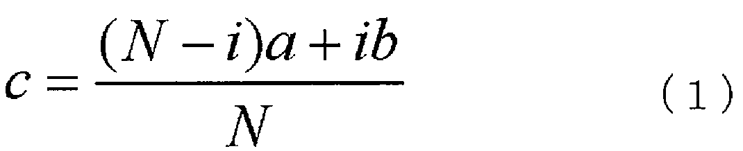
이러한 방법에 의해 생성된 화상 데이터를 사용하여 화상 A에서 화상 B로 전환함으로써, 매끄럽게(조용히), 자연스럽게 불연속의 화상을 전환할 수 있다.By using the image data generated by this method to switch from image A to image B, it is possible to switch discontinuous images smoothly (silently) and naturally.
또한, 수학식 1에 있어서, 모든 화소에 대하여 a=0인 경우가, 흑색 화상에서 서서히 화상 B로 전환되는 페이드 인에 상당한다. 또한, 모든 화소에 대하여 b=0인 경우가, 화상 A에서 서서히 흑색 화상으로 전환되는 페이드 아웃에 상당한다.Also, in
상기에서는, 2개의 화상을 일시적으로 오버랩시켜서 화상을 전환하는 방법에 대하여 서술하였지만, 오버랩시키지 않는 방법으로 하여도 좋다.The above describes a method of switching images by temporarily overlapping two images, but it may also be done in a method that does not overlap them.
2개의 화상을 오버랩시키지 않는 경우, 화상 A에서 화상 B로 전환하는 경우에, 사이에 흑색 화상을 삽입하여도 좋다. 이때, 화상 A에서 흑색 화상으로 전이할 때, 또는 흑색 화상에서 화상 B로 전이할 때, 또는 그 양쪽에 상술한 바와 같은 화상 전환 방법을 사용하여도 좋다. 또한, 화상 A와 화상 B 사이에 삽입하는 화상은 흑색 화상뿐만 아니라, 백색 화상 등의 단일 색의 화상을 사용하여도 좋고, 화상 A나 화상 B는 상이한, 다색의 화상을 사용하여도 좋다.When two images are not overlapped, a black image may be inserted in between when switching from image A to image B. At this time, the image switching method described above may be used when switching from image A to a black image, or when switching from a black image to image B, or on both sides. Furthermore, the image inserted between image A and image B may be a single-color image such as a white image, as well as a black image, and image A and image B may be different, multi-color images.
화상 A와 화상 B 사이에 상이한 화상, 특히 흑색 화상 등의 단일 색의 화상을 삽입함으로써, 화상 전환의 타이밍을 보다 자연스럽게 사용자가 감지할 수 있고, 사용자에게 스트레스를 느끼게 하지 않고 화상을 전환할 수 있다.By inserting a different image, particularly a single-color image such as a black image, between images A and B, the timing of the image transition can be perceived more naturally by the user, and the images can be switched without causing stress to the user.
또한, 본 실시형태는, 본 명세서에서 나타내는 다른 실시형태와 적절히 조합할 수 있다.In addition, this embodiment can be appropriately combined with other embodiments described in this specification.
(실시형태 8)(Embodiment 8)
본 실시형태에서는, 본 발명의 일 양태의 반도체 장치를 사용한 정보 처리 장치의 구성에 대하여 도 35a1 내지 도 35b2 및 도 36을 참조하면서 설명한다.In this embodiment, the configuration of an information processing device using a semiconductor device of one aspect of the present invention will be described with reference to FIGS. 35a1 to 35b2 and FIG. 36.
도 35a1 내지 도 35b2는 정보 처리 장치의 효과를 설명하는 도면이다.Figures 35a1 to 35b2 are drawings explaining the effects of an information processing device.
도 36은 정보 처리 장치의 구성을 설명하는 블록도이다.Figure 36 is a block diagram explaining the configuration of an information processing device.
눈의 피로에는 신경계의 피로와 근육계의 피로 2종류가 있다. 눈의 피로를 설명하는 모식도를 도 35a에 도시한다.There are two types of eye fatigue: nervous system fatigue and muscular system fatigue. A schematic diagram explaining eye fatigue is shown in Figure 35a.
신경계의 피로는, 표시부가 발하는 광이나 점멸 화면을 장시간 동안 계속하여 봄으로써 그 밝기가 눈의 망막, 신경 또는 뇌를 자극하여 피로하게 하는 것이다. 형광등이나 종래의 표시 장치의 표시부가 조금씩 명멸(明滅)하는 현상을 플리커라고 하지만, 이러한 플리커는 신경계의 피로를 일으킨다.Fatigue of the nervous system occurs when the brightness of a display or a flashing screen stimulates the retina, nerves, or brain, causing fatigue, as a result of continuously looking at it for a long time. The phenomenon of the display of a fluorescent lamp or a conventional display device gradually flickering is called flicker, and this flicker causes fatigue of the nervous system.
근육계의 피로는, 핀트 조절시에 사용하는 모양체(毛樣體)의 근육을 혹사함으로써 피로하게 하는 것이다.Muscular fatigue occurs when the ciliary muscles, which are used to adjust the pint, are overworked.
도 35a1에, 종래의 표시부의 표시를 나타내는 모식도를 도시한다. 종래의 표시부는 1초간에 60회 화상의 재기록이 행하여지고 있다. 이러한 화면을 장시간 동안 계속하여 봄으로써 사용자의 눈의 망막, 신경 또는 뇌를 자극하여 눈의 피로가 야기될 우려가 있다.Fig. 35a1 shows a schematic diagram showing the display of a conventional display unit. In a conventional display unit, images are re-recorded 60 times per second. There is a concern that if such a screen is continuously viewed for a long period of time, the user's retina, nerves, or brain may be stimulated, causing eye fatigue.
또한, 도 35a2에 도시한 바와 같이 1화소의 사이즈가 큰 경우(예를 들면, 세밀도가 150ppi 미만인 경우), 표시부에 표시된 문자 등의 윤곽이 희미해져 버린다. 표시부에 표시된 윤곽이 희미해진 문자 등을 장시간 동안 계속하여 보면, 모양체의 근육이 끊임없이 핀트를 맞추려고 움직여서 계속 긴장됨으로써, 눈에 부담을 가해버릴 우려가 있다.In addition, as shown in Fig. 35a2, when the size of one pixel is large (for example, when the resolution is less than 150 ppi), the outlines of characters, etc. displayed on the display become blurred. If you continue to look at characters, etc. with blurred outlines displayed on the display for a long time, there is a risk that the ciliary muscles will constantly move to focus and become continuously tense, which may put a strain on the eyes.
또한, 눈의 피로를 정량적으로 측정하는 방법이 검토되고 있다. 예를 들면, 신경계 피로의 평가 지표로서는 임계 융합 주파수(CFF: Critical Flicker(Fusion) Frequency) 등이 알려져 있다. 또한, 근육계 피로의 평가 지표로서는 조절 시간이나 조절 근점 거리 등이 알려져 있다.In addition, methods for quantitatively measuring eye fatigue are being reviewed. For example, the critical flicker (fusion) frequency (CFF) is known as an evaluation index for nervous system fatigue. In addition, accommodation time and accommodative near point distance are known as evaluation indexes for muscular system fatigue.
그 밖에, 눈의 피로를 평가하는 방법으로서 뇌파 측정, 서모그래피법, 깜박임 회수의 측정, 눈물액량의 평가, 동공의 수축 반응 속도의 평가나, 자각 증상을 조사하기 위한 앙케트 등이 있다.In addition, there are methods to evaluate eye fatigue, such as electroencephalography, thermography, measurement of blink frequency, evaluation of tear volume, evaluation of pupillary constriction reaction speed, and questionnaires to investigate subjective symptoms.
상기 과제를 해결하기 위하여, 본 발명의 일 양태는 작업 환경의 조도와 표시 장치에 표시되는 화상 정보의 배경의 계조에 착안하였다. 이하에 설명하는 실시형태에는, 환경의 조도 정보와 화상 정보 배경의 계조 정보에 착안하여 창작된 본 발명의 일 양태가 포함된다.In order to solve the above problem, one embodiment of the present invention focuses on the illuminance of a work environment and the gradation of the background of image information displayed on a display device. The embodiment described below includes one embodiment of the present invention created by focusing on the illuminance information of the environment and the gradation information of the background of image information.
본 발명의 일 양태의 화상 정보의 처리 및 표시 방법은, 환경의 조도 정보 및 표시부에 표시하는 화상 정보 배경의 계조 정보를 취득하는 스텝과, 이들 정보를 사용하여 화상 정보를, 표시광에 420nm보다 짧은 파장의 광을 포함하지 않고 또한 150ppi 이상의 세밀도로 설치된 복수의 화소를 구비하는 표시부에 표시하는 스텝을 갖는다. 이에 의해, 화상 정보를 환경의 조도에 알맞은 밝기로 표시할 수 있다. 그 결과, 화상 정보의 처리 및 눈이 편한 표시를 할 수 있는 신규의 화상 정보의 처리 및 표시 방법을 제공할 수 있다.A method for processing and displaying image information according to one aspect of the present invention comprises the steps of acquiring environmental illuminance information and gradation information of a background of image information to be displayed on a display unit, and the step of using these pieces of information to display image information on a display unit having a plurality of pixels that do not include light of a shorter wavelength than 420 nm in display light and are provided with a precision of 150 ppi or more. As a result, the image information can be displayed at brightness appropriate for the environmental illuminance. As a result, a novel method for processing and displaying image information capable of processing image information and displaying it in a manner that is easy on the eyes can be provided.
본 발명의 일 양태의 화상 정보의 처리 및 표시 방법을 적용할 수 있는 정보 처리 장치의 블록도의 일례를 도 36에 도시한다.An example of a block diagram of an information processing device to which the image information processing and display method of one aspect of the present invention can be applied is illustrated in FIG. 36.
정보 처리 장치(330)는 연산부(311), 기억부(312) 및 전송로(314)를 갖는다. 전송로(314)는 연산부(311), 기억부(312) 및 입출력 인터페이스(315)를 서로 접속하고, 정보의 전송을 행한다. 또한, 이들 구성은 명확하게 분리할 수 없고, 하나의 구성이 다른 구성을 겸하는 경우나 다른 구성의 일부를 포함하는 경우가 있다. 예를 들면, 터치 패널은 표시부임과 동시에 입력 수단이기도 한다.The information processing device (330) has an operation unit (311), a memory unit (312), and a transmission line (314). The transmission line (314) connects the operation unit (311), the memory unit (312), and the input/output interface (315) to each other and transmits information. In addition, these configurations cannot be clearly separated, and there are cases where one configuration combines with another configuration or includes a part of another configuration. For example, a touch panel is both a display unit and an input means.
입출력 장치(320)는, 입출력 인터페이스(315)를 통하여 전송로(314)에 접속된다. 입출력 장치(320)는 연산 장치(310)의 외부에서 정보를 입력 또는 연산 장치(310)의 외부에 정보를 출력하기 위한 장치이다.The input/output device (320) is connected to the transmission line (314) via the input/output interface (315). The input/output device (320) is a device for inputting information from outside the calculation device (310) or outputting information to the outside of the calculation device (310).
입출력 장치(320)로서는, 통신 기기, 네트워크 접속 기기 또는 하드 디스크, 리무버블 메모리 등 기록 가능한 외부 기억부를 그 일례로서 들 수 있다.As input/output devices (320), examples thereof include communication devices, network connection devices, or recordable external memory devices such as hard disks and removable memories.
입력 수단(321)으로서는, 키보드, 마우스 또는 터치 패널 등의 휴먼 인터페이스 기기, 디지털 카메라, 디지털 비디오 카메라 등의 카메라, 스캐너, CDROM, DVDROM 등 판독 전용의 외부 기억부를 그 일례로서 들 수 있다. 예를 들면, 정보 처리 장치(330)의 사용자는, 입력 수단(321)에서 페이지 넘김 명령 등을 입력할 수 있다.As input means (321), examples thereof include human interface devices such as a keyboard, mouse, or touch panel, cameras such as digital cameras or digital video cameras, scanners, and read-only external memory devices such as CDROMs or DVDROMs. For example, a user of an information processing device (330) can input page-turning commands, etc., through the input means (321).
출력 장치로서는 표시부(322) 이외에, 스피커, 프린터 등을 접속할 수 있다.In addition to the display unit (322), speakers, printers, etc. can be connected as output devices.
본 발명의 일 양태의 정보 처리 장치(330)는 표시부(322)를 구비한다. 특히, 표시부(322)는, 표시광에 420nm보다 짧은 파장의 광, 바람직하게는 440nm보다 단파장의 광을 포함하지 않는다. 그리고, 표시 영역에 150ppi 이상, 바람직하게는 200ppi 이상의 세밀도로 설치된 복수의 화소를 구비하면 좋다. 이에 의해, 눈이 편한 표시를 하는 것이 가능하게 된다. 또한, 본 명세서에서 표시광이란, 정보 처리 장치의 표시부가 화상을 표시하기 위하여 사용자를 향하여 발하는, 또는 반사하는 광을 말한다.An information processing device (330) of one aspect of the present invention comprises a display portion (322). In particular, the display portion (322) does not include light having a wavelength shorter than 420 nm, preferably light having a wavelength shorter than 440 nm, in the display light. In addition, it is preferable that a plurality of pixels be provided in the display area with a precision of 150 ppi or more, preferably 200 ppi or more. This makes it possible to provide a display that is easy on the eyes. In addition, in this specification, the display light refers to light that the display portion of the information processing device emits or reflects toward the user in order to display an image.
본 발명의 일 양태에 관한 표시부의 표시광은, 눈의 각막이나 수정체에서 흡수되지 않고 망막까지 도달하기 때문에, 장기적인 망막에 대한 영향이나, 생체 리듬에 대한 악영향이 있는 광을 포함하지 않는다. 구체적으로는, 화상을 표시하는 광에 400nm, 바람직하게는 420nm, 보다 바람직하게는 440nm 이하의 파장을 갖는 광(UVA라고도 한다)을 포함하지 않는다.The display light of the display unit according to one embodiment of the present invention does not contain light that has a long-term effect on the retina or a negative effect on the biological rhythm because it reaches the retina without being absorbed by the cornea or lens of the eye. Specifically, the light for displaying an image does not contain light having a wavelength of 400 nm, preferably 420 nm, and more preferably 440 nm or less (also called UVA).
본 발명의 일 양태의 정보 처리 장치(330)에는 본 발명의 일 양태의 반도체 장치를 사용할 수 있다. 상기 반도체 장치에 있어서의 화소에서는, 상기 파장을 갖는 광을 흡수하고, 투과하기 어려운 특징을 갖는다. 따라서, 상기 파장을 갖는 광을 발하는 광원을 사용하여도, 본 발명의 일 양태의 반도체 장치를 사용함으로써 상기 파장을 갖는 광을 저감 또는 차단할 수 있다.The information processing device (330) of one aspect of the present invention can use the semiconductor device of one aspect of the present invention. The pixel in the semiconductor device has the characteristic of absorbing light having the above wavelength and making it difficult to transmit it. Therefore, even if a light source that emits light having the above wavelength is used, the light having the above wavelength can be reduced or blocked by using the semiconductor device of one aspect of the present invention.
또한, 본 발명의 일 양태에 관한 표시부가 구비하는 화소의 세밀도가 150ppi, 바람직하게는 200ppi 이상이고, 1화소의 사이즈가 작다. 이에 의해, 사용자의 눈의 근육계의 피로가 경감된다.In addition, the display unit according to one embodiment of the present invention has a pixel resolution of 150 ppi or higher, preferably 200 ppi or higher, and the size of one pixel is small. As a result, fatigue of the user's eye muscles is reduced.
본 발명의 일 양태의 정보 처리 장치의 눈의 피로를 경감시키는 효과를 설명하는 모식도를 도 35b에 도시한다.A schematic diagram explaining the effect of reducing eye fatigue of an information processing device of one aspect of the present invention is shown in Fig. 35b.
본 발명의 일 양태의 정보 처리 장치는 화소를 선택하는 신호를 출력하는 빈도를 바꿀 수 있다. 특히, 오프 전류가 상당히 작은 트랜지스터를 표시부의 화소부에 사용함으로써 플리커의 발생을 억제하면서 프레임 주파수를 낮출 수 있다. 예를 들면, 5초간에 1회 화상의 재기록이 가능해지기 때문에, 같은 화상을 보는 것이 가능해지고, 사용자에게 시인되는 화면의 어른거림이 저감된다. 이에 의해, 사용자의 눈의 망막, 신경 또는 뇌가 받는 자극이 저감되어, 신경계의 피로가 경감된다(도 35b1 참조).An information processing device according to one aspect of the present invention can change the frequency at which a signal for selecting a pixel is output. In particular, by using a transistor having a considerably small off-current in a pixel portion of a display portion, the frame frequency can be lowered while suppressing the occurrence of flicker. For example, since it becomes possible to rewrite an image once every 5 seconds, it becomes possible to view the same image, and the flickering of the screen perceived by the user is reduced. As a result, the stimulation received by the retina, nerves, or brain of the user's eyes is reduced, and fatigue of the nervous system is alleviated (see Fig. 35b1).
또한, 오프 전류가 상당히 작은 트랜지스터로서는, 예를 들면, 산화물 반도체를 사용한 트랜지스터, 특히, CAAC-OS를 사용한 트랜지스터가 적합하다.Also, as a transistor with a relatively small off-state current, for example, a transistor using an oxide semiconductor, especially a transistor using CAAC-OS, is suitable.
본 발명의 일 양태의 정보 처리 장치는 1화소의 사이즈가 작다. 구체적으로는, 세밀도가 150ppi, 바람직하게는 200ppi 이상의 고정밀한 표시가 가능하다. 화상의 윤곽을 명료하게, 또한 치밀하고 매끄럽게 표시할 수 있다. 이에 의해, 모양체의 근육이 핀트를 맞추기가 쉬워지기 때문에, 사용자의 근육계의 피로가 경감된다(도 35b2 참조). 또한, 세밀도는 화소 밀도(ppi: pixcel per inch)를 사용하여 표현할 수 있다. 화소 밀도는 1인치당 화소의 수이다. 또한, 화소는 화상을 구성하는 단위이다.An information processing device according to one aspect of the present invention has a small pixel size. Specifically, high-precision display with a resolution of 150 ppi, preferably 200 ppi or more is possible. The outline of an image can be displayed clearly, densely and smoothly. As a result, since the muscles of the ciliary body become easier to focus, fatigue of the user's muscular system is reduced (see Fig. 35b2). In addition, the resolution can be expressed using pixel density (ppi: pixels per inch). The pixel density is the number of pixels per inch. In addition, a pixel is a unit constituting an image.
또한, 본 실시형태는, 본 명세서에서 나타내는 다른 실시형태와 적절히 조합할 수 있다.In addition, this embodiment can be appropriately combined with other embodiments described in this specification.
(실시형태 9)(Embodiment 9)
본 발명의 일 양태인 반도체 장치는 다양한 전자 기기(게임기도 포함한다)에 적용할 수 있다. 전자 기기로서는, 텔레비전 장치, 컴퓨터용 등의 모니터, 디지털 카메라, 디지털 비디오 카메라, 디지털 포토 프레임, 휴대 전화기, 게임기, 휴대형 게임기, 휴대 정보 단말, 음향 재생 장치, 게임기(파친코기, 슬롯 머신 등)를 들 수 있다. 이들 전자 기기의 일례를 도 37a 내지 도 37c, 도 38a 및 도 38b에 도시한다.The semiconductor device according to one aspect of the present invention can be applied to various electronic devices (including game machines). As the electronic devices, there can be mentioned television devices, monitors for computers, digital cameras, digital video cameras, digital photo frames, mobile phones, game machines, portable game machines, portable information terminals, audio reproduction devices, and game machines (pachinko machines, slot machines, etc.). Examples of these electronic devices are shown in FIGS. 37a to 37c, FIGS. 38a and 38b.
도 37a는 표시부를 갖는 테이블을 도시하고 있다. 테이블(9000)은 케이싱 (9001)에 표시부(9003)가 내장되어 있고, 표시부(9003)에 의해 영상을 표시하는 것이 가능하다. 또한, 4개의 다리부(9002)에 의해 케이싱(9001)을 지지한 구성을 도시하고 있다. 또한, 전력 공급을 위한 전원 코드(9005)를 케이싱(9001)에 갖고 있다.Fig. 37a illustrates a table having a display portion. The table (9000) has a display portion (9003) built into a casing (9001), and is capable of displaying an image by the display portion (9003). In addition, a configuration in which the casing (9001) is supported by four leg portions (9002) is illustrated. In addition, a power cord (9005) for supplying power is provided in the casing (9001).
상기 실시형태 중 어느 하나에 나타낸 반도체 장치는 표시부(9003)에 사용하는 것이 가능하다. 그 때문에, 표시부(9003)의 표시 품질을 높게 할 수 있다.The semiconductor device shown in any one of the above embodiments can be used in the display portion (9003). Therefore, the display quality of the display portion (9003) can be improved.
표시부(9003)는 터치 입력 기능을 가지며, 테이블(9000)의 표시부(9003)에 표시된 표시 버튼(9004)을 손가락 등으로 터치함으로써 화면을 조작하거나 정보를 입력할 수 있고, 또한 다른 가전 제품과의 통신을 가능하게 하는, 또는 제어를 가능하게 함으로써 화면 조작에 의해 다른 가전 제품을 컨트롤하는 제어 장치로 하여도 좋다. 예를 들면, 터치 센서 기능이나 이미지 센서 기능을 갖는 반도체 장치를 사용하면, 표시부(9003)에 터치 입력 기능을 부여할 수 있다.The display unit (9003) has a touch input function, and by touching the display button (9004) displayed on the display unit (9003) of the table (9000) with a finger or the like, the screen can be operated or information can be input, and also, it can be used as a control device that enables communication with other home appliances or enables control, thereby controlling other home appliances by screen operation. For example, by using a semiconductor device having a touch sensor function or an image sensor function, the display unit (9003) can be provided with a touch input function.
또한, 케이싱(9001)에 설치된 힌지에 의해 표시부(9003)의 화면을 바닥에 수직으로 세울 수도 있고, 텔레비전 장치로서도 이용할 수 있다. 좁은 방에서는 화면이 큰 텔레비전 장치는 설치하면 자유 공간이 좁아지지만, 테이블에 표시부가 내장되어 있으면 방의 공간을 유효하게 이용할 수 있다.In addition, the screen of the display unit (9003) can be placed vertically on the floor by a hinge installed in the casing (9001), and can also be used as a television device. In a narrow room, if a television device with a large screen is installed, the free space becomes narrow, but if the display unit is built into the table, the space of the room can be effectively used.
도 37b는 텔레비전 장치를 도시하고 있다. 텔레비전 장치(9100)는 케이싱 (9101)에 표시부(9103)가 내장되어 있고, 표시부(9103)에 의해 영상을 표시하는 것이 가능하다. 또한, 여기에서는 스탠드(9105)에 의해 케이싱(9101)을 지지한 구성을 도시하고 있다.Fig. 37b illustrates a television device. The television device (9100) has a display portion (9103) built into a casing (9101), and is capable of displaying images by the display portion (9103). In addition, this illustrates a configuration in which the casing (9101) is supported by a stand (9105).
텔레비전 장치(9100)의 조작은 케이싱(9101)이 구비한 조작 스위치나, 별개의 리모트 컨트롤러(9110)에 의해 행할 수 있다. 리모트 콘트롤러(9110)가 구비한 조작키(9109)에 의해 채널이나 음량을 조작할 수 있고, 표시부(9103)에 표시되는 영상을 조작할 수 있다. 또한, 리모트 콘트롤러(9110)에, 상기 리모트 콘트롤러로부터 출력하는 정보를 표시하는 표시부(9107)를 설치하는 구성으로 하여도 좋다.The television device (9100) can be operated by an operation switch provided in the casing (9101) or a separate remote controller (9110). The channel or volume can be operated by the operation keys (9109) provided in the remote controller (9110), and the image displayed on the display section (9103) can be operated. In addition, a configuration may be adopted in which a display section (9107) for displaying information output from the remote controller is installed in the remote controller (9110).
도 37b에 도시한 텔레비전 장치(9100)는 수신기나 통신 수단 등을 구비하고 있다. 텔레비전 장치(9100)는 수신기에 의해 일반적인 텔레비전 방송을 수신할 수 있고, 또한 통신 수단을 통하여 유선 또는 무선에 의한 통신 네트워크에 접속함으로써 일방향(송신자로부터 수신자) 또는 쌍방향(송신자와 수신자 사이 또는 수신자들 사이 등)의 정보 통신을 행하는 것도 가능하다.The television device (9100) illustrated in Fig. 37b is equipped with a receiver, communication means, etc. The television device (9100) can receive general television broadcasting by the receiver, and also can perform one-way (from transmitter to receiver) or two-way (between transmitter and receiver or between receivers, etc.) information communication by connecting to a wired or wireless communication network through the communication means.
상기 실시형태 중 어느 하나에 나타낸 반도체 장치는 표시부(9103, 9107)에 사용하는 것이 가능하다. 그 때문에, 텔레비전 장치의 표시 품질을 향상시킬 수 있다.The semiconductor device shown in any one of the above embodiments can be used in the display portion (9103, 9107). Therefore, the display quality of the television device can be improved.
도 37c는 컴퓨터(9200)이고, 본체(9201), 케이싱(9202), 표시부(9203), 키보드(9204), 외부 접속 포트(9205), 포인팅 디바이스(9206) 등을 포함한다.FIG. 37c is a computer (9200), which includes a main body (9201), a casing (9202), a display unit (9203), a keyboard (9204), an external connection port (9205), a pointing device (9206), etc.
상기 실시형태 중 어느 하나에 나타낸 반도체 장치는 표시부(9203)에 사용하는 것이 가능하다. 그 때문에, 컴퓨터(9200)의 표시 품질을 향상시킬 수 있다.The semiconductor device shown in any one of the above embodiments can be used in the display portion (9203). Therefore, the display quality of the computer (9200) can be improved.
표시부(9203)는 터치 입력 기능을 갖고 있고, 표시부(9203)에 표시된 표시 버튼 등을 손가락 등으로 터치함으로써 화면 조작이나 정보를 입력할 수 있다. 또한, 키보드나 음성으로 정보를 입력할 수 있다.The display unit (9203) has a touch input function, and screen operation or information input can be performed by touching display buttons, etc. displayed on the display unit (9203) with a finger or the like. In addition, information can be input using a keyboard or voice.
도 38a 및 도 38b는 접이식 가능한 태블릿형 단말이다. 도 38a는 연 상태이고, 태블릿형 단말은 케이싱(9630), 표시부(9631a), 표시부(9631b), 표시 모드 전환 스위치(9034), 전원 스위치(9035), 전력 절약 모드 전환 스위치(9036), 잠금쇠(9033), 조작 스위치(9038)를 갖는다.Figures 38a and 38b show a foldable tablet-type terminal. Figure 38a is in an open state, and the tablet-type terminal has a casing (9630), a display portion (9631a), a display portion (9631b), a display mode switching switch (9034), a power switch (9035), a power saving mode switching switch (9036), a lock (9033), and an operation switch (9038).
상기 실시형태 중 어느 하나에 나타낸 반도체 장치는, 표시부(9631a), 표시부(9631b)에 사용하는 것이 가능하다. 그 때문에, 태블릿 단말의 표시 품질을 향상시킬 수 있다.The semiconductor device shown in any one of the above embodiments can be used in the display portion (9631a) and the display portion (9631b). Therefore, the display quality of the tablet terminal can be improved.
표시부(9631a)는, 일부를 터치 패널의 영역(9632a)으로 할 수 있고, 표시된 조작 키(9638)에 터치함으로서 데이터 입력을 할 수 있다. 또한, 표시부(9631a)에 서는, 일례로서 절반의 영역이 표시 기능만을 갖는 구성, 나머지 절반의 영역이 터치 패널의 기능을 갖는 구성을 나타내고 있지만 상기 구성에 한정되지 않는다. 표시부(9631a)의 모든 영역이 터치 패널의 기능을 갖는 구성으로 하여도 좋다. 예를 들면, 표시부(9631a)의 전면을 키보드 버튼 표시시켜서 터치 패널로 하고, 표시부(9631b)를 표시 화면으로 하여 사용할 수 있다.The display portion (9631a) can have a part as a touch panel area (9632a), and data can be input by touching the displayed operation key (9638). In addition, the display portion (9631a) shows a configuration in which half of the area has only a display function and the other half of the area has a touch panel function, as an example, but is not limited to the above configuration. The entire area of the display portion (9631a) may have a touch panel function. For example, the entire surface of the display portion (9631a) can be used as a touch panel by displaying keyboard buttons, and the display portion (9631b) can be used as a display screen.
또한, 표시부(9631b)에서도 표시부(9631a)와 같이, 표시부(9631b)의 일부를 터치 패널의 영역(9632b)으로 할 수 있다. 또한, 터치 패널의 키보드 표시 전환 버튼(9639)이 표시되어 있는 위치에 손가락이나 스타일러스(stylus) 등으로 터치함으로써 표시부(9631b)에 키보드 버튼 표시할 수 있다.In addition, in the display portion (9631b), as in the display portion (9631a), a part of the display portion (9631b) can be made into a touch panel area (9632b). In addition, by touching the location where the keyboard display switching button (9639) of the touch panel is displayed with a finger or a stylus, a keyboard button can be displayed on the display portion (9631b).
또한, 터치 패널의 영역(9632a)과 터치 패널의 영역(9632b)에 대하여 동시에 터치 입력할 수도 있다.Additionally, touch input can be performed simultaneously on the area of the touch panel (9632a) and the area of the touch panel (9632b).
또한, 표시 모드 전환 스위치(9034)는 세로 표시 또는 가로 표시 등의 표시 방향을 전환, 흑백 표시나 컬러 표시의 전환 등을 선택할 수 있다. 전력 절약 모드 전환 스위치(9036)는, 태블릿형 단말에 내장되어 있는 광센서에서 검출되는 사용시의 외광의 광량에 따라 표시의 휘도를 최적인 것으로 할 수 있다. 태블릿형 단말은 광센서뿐만 아니라, 자이로스코프(gyroscope), 가속도 센서 등의 경사를 검출하는 센서 등의 다른 검출 장치를 내장시켜도 좋다.In addition, the display mode switching switch (9034) can select to switch the display direction, such as vertical display or horizontal display, and to switch between black and white display or color display. The power saving mode switching switch (9036) can optimize the display brightness according to the amount of external light detected by the light sensor built into the tablet terminal during use. The tablet terminal may have built-in not only the light sensor, but also other detection devices, such as a sensor that detects inclination, such as a gyroscope or an acceleration sensor.
또한, 도 38a에서는 표시부(9631b)와 표시부(9631a)의 표시 면적이 같은 예를 도시하고 있지만 특별히 한정되지 않고, 한쪽의 사이즈와 다른 한쪽의 사이즈가 상이하여도 좋고, 표시의 품질도 상이하여도 좋다. 예를 들면, 한쪽이 다른 한쪽보다도 고정밀한 표시를 행할 수 있는 표시 패널로 하여도 좋다.In addition, although Fig. 38a shows an example in which the display areas of the display portions (9631b) and the display portions (9631a) are the same, there is no particular limitation, and the sizes of one side and the other side may be different, and the quality of the display may also be different. For example, it may be a display panel in which one side can perform a higher-precision display than the other side.
도 38b는 닫은 상태이고, 태블릿형 단말은 케이싱(9630)에 태양 전지(9633), 충방전 제어 회로(9634)를 갖고 있어도 좋다. 또한, 도 38b에서는 충방전 제어 회로(9634)의 일례로서 배터리(9635), DCDC 컨버터(9636)를 갖는 구성에 대하여 도시하고 있다.Fig. 38b is in a closed state, and the tablet-type terminal may have a solar cell (9633) and a charge/discharge control circuit (9634) in the casing (9630). In addition, Fig. 38b illustrates a configuration having a battery (9635) and a DCDC converter (9636) as an example of the charge/discharge control circuit (9634).
또한, 태블릿형 단말은 접이식 가능하기 때문에, 미사용시에 케이싱(9630)을 닫은 상태로 할 수 있다. 따라서, 표시부(9631a), 표시부(9631b)를 보호할 수 있으므로 내구성이 우수하고, 장기 사용의 관점에서도 신뢰성이 우수한 태블릿형 단말을 제공할 수 있다.In addition, since the tablet-type terminal is foldable, the casing (9630) can be closed when not in use. Accordingly, the display portion (9631a) and the display portion (9631b) can be protected, so that a tablet-type terminal with excellent durability and reliability from the perspective of long-term use can be provided.
또한, 이 밖에도 도 38a 및 도 38b에 도시한 태블릿형 단말은, 여러가지 정보(정지 화상, 동영상, 텍스트 화상 등)를 표시하는 기능, 카렌다, 날짜 또는 시간 등을 표시부에 표시하는 기능, 표시부에 표시한 정보를 터치 입력 조작 또는 편집하는 터치 입력 기능, 여러가지 소프트웨어(프로그램)에 의해 처리를 제어하는 기능 등을 갖을 수 있다.In addition, the tablet terminal illustrated in FIGS. 38a and 38b may have a function for displaying various information (still images, moving images, text images, etc.), a function for displaying a calendar, date or time, etc. on the display unit, a touch input function for performing touch input operations or editing information displayed on the display unit, a function for controlling processing by various software (programs), etc.
태블릿형 단말의 표면에 장착된 태양 전지(9633)에 의해, 전력을 터치 패널, 표시부, 또는 영상 신호 처리부 등에 공급할 수 있다. 또한, 태양 전지(9633)는 케이싱(9630)의 한 면 또는 양면에 설치할 수 있고, 배터리(9635)의 충전을 효율적으로 행할 수 있다. 또한 배터리(9635)로서는 리튬 이온 전지를 사용하면 소형화를 도모할 수 있는 등의 이점이 있다.By means of a solar cell (9633) mounted on the surface of a tablet terminal, power can be supplied to a touch panel, a display unit, or an image signal processing unit. In addition, the solar cell (9633) can be installed on one or both sides of the casing (9630), and can efficiently charge the battery (9635). In addition, there is an advantage in that miniaturization can be achieved by using a lithium ion battery as the battery (9635).
또한, 도 38b에 도시한 충방전 제어 회로(9634)의 구성 및 동작에 대하여 도 39a 내지 도 39c에 블록도를 도시하여 설명한다. 도 39a에서는 태양 전지(9633), 배터리(9635), DCDC 컨버터(9636), DCDC 컨버터(9637), 스위치(SW1 내지 SW3), 부하(표시부(9631) 등)에 대하여 도시하고 있고, 배터리(9635), DCDC 컨버터(9636), DCDC 컨버터(9637), 스위치(SW1 내지 SW3)가 도 38b에 도시한 충방전 제어 회로(9634)에 대응하는 개소가 된다.In addition, the configuration and operation of the charge/discharge control circuit (9634) illustrated in Fig. 38b will be described with reference to block diagrams illustrated in Figs. 39a to 39c. Fig. 39a illustrates a solar cell (9633), a battery (9635), a DCDC converter (9636), a DCDC converter (9637), switches (SW1 to SW3), and a load (display section (9631), etc.), and the battery (9635), the DCDC converter (9636), the DCDC converter (9637), and the switches (SW1 to SW3) correspond to the charge/discharge control circuit (9634) illustrated in Fig. 38b.
우선, 태양 전지(9633)에 의해 발전이 되는 경우의 동작의 예에 대하여 설명한다. 태양 전지에서 발전한 전력은, 배터리(9635)를 충전하기 위한 전압이 되도록 DCDC 컨버터(9636)로 승압 또는 강압이 된다. 그리고, 부하(표시부(9631) 등)의 동작에 태양 전지(9633)로부터의 전력이 사용될 때는 스위치(SW1)를 온으로 하고, DCDC 컨버터(9637)로 부하(표시부(9631) 등)에 필요한 전압에 승압 또는 강압을 하는 것으로 된다. 또한, 부하(표시부(9631) 등)로의 전력의 공급을 행하지 않을 때에는 SW1을 오프로하고, SW2를 온으로 하여 배터리(9635)의 충전을 행하는 구성으로 하면 좋다.First, an example of operation when power is generated by a solar cell (9633) will be described. The power generated by the solar cell is boosted or lowered by a DCDC converter (9636) so as to become a voltage for charging a battery (9635). Then, when power from the solar cell (9633) is used for the operation of a load (such as a display unit (9631)), the switch (SW1) is turned on, and the DCDC converter (9637) is used to boost or lower the voltage required for the load (such as a display unit (9631)). In addition, when power is not supplied to the load (such as a display unit (9631)), it is preferable to configure it so that SW1 is turned off, SW2 is turned on, and the battery (9635) is charged.
또한, 부하(표시부(9631) 등)로의 전력 공급을 항상 배터리(9635)를 통하여 행하는 경우에는, 도 39b에 도시한 바와 같이 스위치(SW1)를 생략한 구성으로 하여도 좋다.In addition, in the case where power supply to the load (such as the display unit (9631)) is always performed through the battery (9635), a configuration in which the switch (SW1) is omitted may be adopted as shown in Fig. 39b.
또한, 부하에 공급하는 적절한 전압 범위와 배터리(9635)의 전압이 동등한 경우에는, 도 39c에 도시한 바와 같이 더욱 DCDC 컨버터(9637)를 생략한 구성으로 하여도 좋다.In addition, if the voltage range supplied to the load is equal to the voltage of the battery (9635), a configuration may be adopted in which the DCDC converter (9637) is omitted, as shown in Fig. 39c.
또한, 태양 전지(9633)에 대하여는 발전 수단의 일례로서 나타냈지만 특별히 한정되지 않고, 압전 소자(피에조 소자(piezoelectric element))나 열전 변환 소자(펠티에 소자(Peltier element)) 등의 다른 발전 수단에 의한 배터리(9635)의 충전을 행하는 구성이라도 좋다. 예를 들면, 무선(비접촉)으로 전력을 송수신하여 충전하는 무접점 전력 전송 모듈이나, 또 다른 충전 수단을 조합하여 행하는 구성으로 하여도 좋다.In addition, although the solar cell (9633) is shown as an example of a power generation means, it is not particularly limited, and a configuration in which the battery (9635) is charged by another power generation means such as a piezoelectric element or a thermoelectric conversion element (Peltier element) may be used. For example, a non-contact power transmission module that wirelessly (non-contact) transmits and receives power to charge, or a configuration in which it is performed in combination with another charging means may be used.
또한, 본 실시형태에 나타낸 구성 등은 다른 실시형태에 나타낸 구성과 적절히 조합하여 사용할 수 있다.In addition, the configurations shown in this embodiment can be used in appropriate combination with the configurations shown in other embodiments.
100 화소부
101 화소
102 기판
103 트랜지스터
104 제 1 구동 회로
105 용량 소자
106 제 2 구동 회로
107 주사선
108 액정 소자
109 신호선
110 질화 절연막
111 반도체막
113 도전막
115 용량선
117 개구
119 반도체막
121 화소 전극
123 개구
125 도전막
127 게이트 절연막
129 절연막
131 절연막
132 절연막
135 경계
150 채널 보호막
154 대향 전극
188a 산화물 반도체막
188b 산화물 반도체막
199a 산화물 반도체막
199b 산화물 반도체막
199c 산화물 반도체막
223 트랜지스터
227 게이트 전극
229 배선
231 반도체막
233 배선
241 도전막
310 연산 장치
311 연산부
312 기억부
314 전송로
315 입출력 인터페이스
320 입출력 장치
321 입력 수단
322 표시부
330 정보 처리 장치
500 입력 수단
500_C 신호
600 정보 처리 장치
610 제어부
615_C 2차 제어 신호
615_V 2차 화상 신호
620 연산 장치
625_C 1차 제어 신호
625_V 1차 화상 신호
630 표시부
631 화소부
631a 영역
631b 영역
631c 영역
631p 화소
632 G 구동 회로
632_G G 신호
632a G 구동 회로
632b G 구동 회로
632c G 구동 회로
633 S 구동 회로
633_S S 신호
634 화소 회로
634c 용량 소자
634EL 화소 회로
634t 트랜지스터
634t_1 트랜지스터
634t_2 트랜지스터
635 표시 소자
635EL EL 소자
635LC 액정 소자
640 표시 장치
650 광 공급부
701 연산부
702 기억부
703 제어부
704 표시부
901 기판
902 화소부
903 제 2 구동 회로
904 제 1 구동 회로
905 씰재
906 기판
908 액정층
910 트랜지스터
911 트랜지스터
913 액정 소자
915 접속 단자 전극
916 단자 전극
917 도전막
918 FPC
918b FPC
919 이방성 도전제
922 게이트 절연막
923 절연막
924 절연막
925 씰재
926 용량 소자
927 산화물 반도체막
929 용량선
930 전극
931 전극
932 절연막
933 절연막
934 절연막
935 스페이서
936 용량 소자
971 소스 전극
973 드레인 전극
975 공통 전위선
977 공통 전극
985 공통 전위선
987 공통 전극
9000 테이블
9001 케이싱
9002 다리부
9003 표시부
9004 표시 버튼
9005 전원 코드
9033 도구
9034 스위치
9035 전원 스위치
9036 스위치
9038 조작 스위치
9100 텔레비전 장치
9101 케이싱
9103 표시부
9105 스탠드
9107 표시부
9109 조작 키
9110 리모트 콘트롤러
9200 컴퓨터
9201 본체
9202 케이싱
9203 표시부
9204 키보드
9205 외부 접속 포트
9206 포인팅 디바이스
9630 케이싱
9631 표시부
9631a 표시부
9631b 표시부
9632a 영역
9632b 영역
9633 태양 전지
9634 충방전 제어 회로
9635 배터리
9636 DCDC 컨버터
9637 DCDC 컨버터
9638 조작 키
9639 버튼100 pixel area
101 pixels
102 substrate
103 transistor
104 1st driving circuit
105 capacity element
106 2nd driving circuit
107 injection line
108 liquid crystal elements
109 signal line
110 Nitride Insulator
111 Semiconductor film
113 Challenge
115 capacity line
117 openings
119 Semiconductor film
121 pixel electrode
123 openings
125 Challenge Screen
127 gate insulator
129 Insulating film
131 Insulating film
132 Insulating film
135 boundary
150 channel shield
154 counter electrode
188a oxide semiconductor film
188b oxide semiconductor film
199a oxide semiconductor film
199b oxide semiconductor film
199c oxide semiconductor film
223 transistor
227 Gate Electrode
229 wiring
231 Semiconductor film
233 wiring
241 Challenge
310 operating unit
311 Operation Unit
312 Memory
314 Transmission Line
315 Input/Output Interface
320 Input/Output Devices
321 Input Method
322 display
330 Information Processing Unit
500 Input Methods
500_C signal
600 information processing unit
610 Control Unit
615_C Secondary control signal
615_V 2nd burn signal
620 computing unit
625_C Primary Control Signal
625_V 1st burn signal
630 display
631 pixels
631p pixels
632 G drive circuit
632_G G signal
632a G drive circuit
632b G drive circuit
632c G drive circuit
633 S drive circuit
633_S S signal
634 pixel circuit
634c capacity element
634EL pixel circuit
634t transistor
634t_1 transistor
634t_2 transistor
635 display elements
635EL EL element
635LC liquid crystal element
640 display device
650 light supply
701 Operation Unit
702 Memory
703 Control Unit
704 display section
901 board
902 pixels
903 2nd drive circuit
904 1st driving circuit
905 seal material
906 board
908 liquid crystal layer
910 transistor
911 transistor
913 liquid crystal element
915 connection terminal electrode
916 terminal electrode
917 Challenge
918 FPC
918b FPC
919 Alien Challenge
922 gate insulator
923 Insulating Film
924 Insulating Film
925 seal material
926 capacity element
927 Oxide semiconductor film
929 capacity line
930 electrode
931 electrode
932 Insulating Film
933 Insulating Film
934 Insulating Film
935 spacer
936 capacity element
971 Source Electrode
973 Drain Electrode
975 common potential line
977 common electrode
985 common potential line
987 common electrode
9000 tables
9001 casing
9002 Bridge Section
9003 display
9004 display button
9005 Power Cord
9033 tools
9034 switch
9035 power switch
9036 switch
9038 operating switch
9100 television device
9101 casing
9103 display
9105 stand
9107 display
9109 Operation Key
9110 remote controller
9200 computer
9201 Body
9202 casing
9203 display
9204 Keyboard
9205 External Access Port
9206 Pointing Device
9630 casing
9631 display
9631a display
9631b display
9633 solar cell
9634 Charge/Discharge Control Circuit
9635 battery
9636 DCDC Converter
9637 DCDC Converter
9638 Control Key
9639 Button
Claims (2)
트랜지스터와, 상기 트랜지스터에 전기적으로 접속되는 용량 소자와, 화소 전극을 갖고,
상기 트랜지스터는, 제 1 산화물 반도체막과, 제 1 도전막과, 제 2 도전막을 갖고,
상기 제 1 도전막은, 상기 트랜지스터의 소스 전극 및 드레인 전극 중 한쪽으로서 기능하는 영역을 갖고,
상기 제 2 도전막은, 상기 트랜지스터의 소스 전극 및 드레인 전극 중 다른 쪽으로서 기능하는 영역을 갖고,
상기 제 1 도전막은, 상기 제 1 산화물 반도체막의 상면과 접하는 영역을 갖고,
상기 제 2 도전막은, 상기 제 1 산화물 반도체막의 상면과 접하는 영역을 갖고,
상기 제 1 산화물 반도체막의 상면과 접하는 영역과, 상기 제 1 도전막의 상면과 접하는 영역과, 상기 제 2 도전막의 상면과 접하는 영역을 갖는 제 1 절연막이 제공되고,
상기 화소 전극은, 상기 제 1 절연막에 제공된 개구를 통하여, 상기 제 2 도전막의 상면과 접하는 영역을 갖고,
상기 용량 소자는, 제 2 산화물 반도체막을 갖고,
상기 제 2 산화물 반도체막은, 상기 용량 소자의 한쪽의 전극으로서 기능하는 영역을 갖고,
상기 제 1 절연막은, 상기 용량 소자의 유전체로서 기능하는 영역을 갖고,
상기 화소 전극은, 상기 용량 소자의 다른 쪽의 전극으로서 기능하는 영역을 갖고,
상기 제 1 절연막은, 상기 제 2 산화물 반도체막의 상면 및 측면과 접하는 영역을 갖고,
상기 제 1 산화물 반도체막 및 상기 제 2 산화물 반도체막의 아래에 제 2 절연막이 제공되고,
상기 제 1 산화물 반도체막은, 상기 제 2 절연막의 상면과 접하는 영역을 갖고,
상기 제 2 산화물 반도체막은, 상기 제 2 절연막의 상면과 접하는 영역을 갖고,
상기 제 2 절연막의 아래에 제 3 도전막이 제공되고,
상기 제 2 산화물 반도체막은, 상기 제 2 절연막을 개재하여 상기 제 3 도전막과 중첩하는 영역을 갖고,
상기 제 1 도전막은, 상기 트랜지스터의 채널 길이 방향과 교차하는 방향으로 연신하는 제 1 영역을 갖고,
상기 제 1 도전막은, 상기 제 1 영역에 있어서, 상기 화소 전극과 중첩하는 영역을 갖는, 표시 장치.As a display device,
Having a transistor, a capacitive element electrically connected to the transistor, and a pixel electrode,
The above transistor has a first oxide semiconductor film, a first conductive film, and a second conductive film,
The above first conductive film has a region that functions as one of the source electrode and the drain electrode of the transistor,
The second conductive film has a region that functions as the other of the source electrode and the drain electrode of the transistor,
The above first challenging film has a region in contact with the upper surface of the first oxide semiconductor film,
The above second challenging film has a region in contact with the upper surface of the first oxide semiconductor film,
A first insulating film is provided, which has a region in contact with the upper surface of the first oxide semiconductor film, a region in contact with the upper surface of the first conductive film, and a region in contact with the upper surface of the second conductive film.
The above pixel electrode has a region that comes into contact with the upper surface of the second conductive film through an opening provided in the first insulating film,
The above capacitor has a second oxide semiconductor film,
The above second oxide semiconductor film has a region that functions as an electrode on one side of the capacitor element,
The above first insulating film has a region that functions as a dielectric of the capacitive element,
The above pixel electrode has a region that functions as the other electrode of the capacitive element,
The above first insulating film has a region in contact with the upper surface and side surface of the second oxide semiconductor film,
A second insulating film is provided beneath the first oxide semiconductor film and the second oxide semiconductor film,
The above first oxide semiconductor film has a region in contact with the upper surface of the second insulating film,
The above second oxide semiconductor film has a region in contact with the upper surface of the second insulating film,
A third conductive film is provided beneath the second insulating film,
The second oxide semiconductor film has a region overlapping with the third conductive film via the second insulating film,
The above first conductive film has a first region extending in a direction intersecting the channel length direction of the transistor,
A display device, wherein the first conductive film has an area overlapping with the pixel electrode in the first area.
상기 제 1 산화물 반도체막은, 산화인듐을 갖고,
상기 제 2 산화물 반도체막은, 산화인듐을 갖는, 표시 장치.In the first paragraph,
The above first oxide semiconductor film has indium oxide,
A display device wherein the second oxide semiconductor film has indium oxide.
Priority Applications (1)
| Application Number | Priority Date | Filing Date | Title |
|---|---|---|---|
| KR1020250165727A KR20250164672A (en) | 2012-12-28 | 2025-11-06 | Semiconductor device and manufacturing method of the same |
Applications Claiming Priority (5)
| Application Number | Priority Date | Filing Date | Title |
|---|---|---|---|
| JP2012288968 | 2012-12-28 | ||
| JPJP-P-2012-288968 | 2012-12-28 | ||
| JP2013049065 | 2013-03-12 | ||
| JPJP-P-2013-049065 | 2013-03-12 | ||
| KR1020240091519A KR102772485B1 (en) | 2012-12-28 | 2024-07-11 | Semiconductor device and manufacturing method of the same |
Related Parent Applications (1)
| Application Number | Title | Priority Date | Filing Date |
|---|---|---|---|
| KR1020240091519A Division KR102772485B1 (en) | 2012-12-28 | 2024-07-11 | Semiconductor device and manufacturing method of the same |
Related Child Applications (1)
| Application Number | Title | Priority Date | Filing Date |
|---|---|---|---|
| KR1020250165727A Division KR20250164672A (en) | 2012-12-28 | 2025-11-06 | Semiconductor device and manufacturing method of the same |
Publications (2)
| Publication Number | Publication Date |
|---|---|
| KR20250031165A true KR20250031165A (en) | 2025-03-06 |
| KR102885398B1 KR102885398B1 (en) | 2025-11-17 |
Family
ID=50928694
Family Applications (9)
| Application Number | Title | Priority Date | Filing Date |
|---|---|---|---|
| KR1020130165904A Active KR102125690B1 (en) | 2012-12-28 | 2013-12-27 | Semiconductor device and manufacturing method of the same |
| KR1020200041486A Active KR102208596B1 (en) | 2012-12-28 | 2020-04-06 | Semiconductor device and manufacturing method of the same |
| KR1020200094970A Active KR102271517B1 (en) | 2012-12-28 | 2020-07-30 | Semiconductor device and manufacturing method of the same |
| KR1020210079884A Active KR102344562B1 (en) | 2012-12-28 | 2021-06-21 | Semiconductor device and manufacturing method of the same |
| KR1020210180273A Active KR102481054B1 (en) | 2012-12-28 | 2021-12-16 | Semiconductor device and manufacturing method of the same |
| KR1020220170693A Active KR102690167B1 (en) | 2012-12-28 | 2022-12-08 | Semiconductor device and manufacturing method of the same |
| KR1020240091519A Active KR102772485B1 (en) | 2012-12-28 | 2024-07-11 | Semiconductor device and manufacturing method of the same |
| KR1020250020674A Active KR102885398B1 (en) | 2012-12-28 | 2025-02-18 | Semiconductor device and manufacturing method of the same |
| KR1020250165727A Pending KR20250164672A (en) | 2012-12-28 | 2025-11-06 | Semiconductor device and manufacturing method of the same |
Family Applications Before (7)
| Application Number | Title | Priority Date | Filing Date |
|---|---|---|---|
| KR1020130165904A Active KR102125690B1 (en) | 2012-12-28 | 2013-12-27 | Semiconductor device and manufacturing method of the same |
| KR1020200041486A Active KR102208596B1 (en) | 2012-12-28 | 2020-04-06 | Semiconductor device and manufacturing method of the same |
| KR1020200094970A Active KR102271517B1 (en) | 2012-12-28 | 2020-07-30 | Semiconductor device and manufacturing method of the same |
| KR1020210079884A Active KR102344562B1 (en) | 2012-12-28 | 2021-06-21 | Semiconductor device and manufacturing method of the same |
| KR1020210180273A Active KR102481054B1 (en) | 2012-12-28 | 2021-12-16 | Semiconductor device and manufacturing method of the same |
| KR1020220170693A Active KR102690167B1 (en) | 2012-12-28 | 2022-12-08 | Semiconductor device and manufacturing method of the same |
| KR1020240091519A Active KR102772485B1 (en) | 2012-12-28 | 2024-07-11 | Semiconductor device and manufacturing method of the same |
Family Applications After (1)
| Application Number | Title | Priority Date | Filing Date |
|---|---|---|---|
| KR1020250165727A Pending KR20250164672A (en) | 2012-12-28 | 2025-11-06 | Semiconductor device and manufacturing method of the same |
Country Status (6)
| Country | Link |
|---|---|
| US (2) | US9196639B2 (en) |
| JP (11) | JP2014199416A (en) |
| KR (9) | KR102125690B1 (en) |
| CN (1) | CN103915447B (en) |
| DE (2) | DE102013022607B4 (en) |
| TW (1) | TWI607510B (en) |
Families Citing this family (35)
| Publication number | Priority date | Publication date | Assignee | Title |
|---|---|---|---|---|
| KR102209871B1 (en) | 2012-12-25 | 2021-02-01 | 가부시키가이샤 한도오따이 에네루기 켄큐쇼 | Semiconductor device |
| KR102440904B1 (en) | 2012-12-28 | 2022-09-05 | 가부시키가이샤 한도오따이 에네루기 켄큐쇼 | Semiconductor device and manufacturing method thereof |
| US9269315B2 (en) | 2013-03-08 | 2016-02-23 | Semiconductor Energy Laboratory Co., Ltd. | Driving method of semiconductor device |
| US9293480B2 (en) | 2013-07-10 | 2016-03-22 | Semiconductor Energy Laboratory Co., Ltd. | Semiconductor device and display device including the semiconductor device |
| KR102244553B1 (en) * | 2013-08-23 | 2021-04-23 | 가부시키가이샤 한도오따이 에네루기 켄큐쇼 | Capacitor and semiconductor device |
| JP2015179247A (en) | 2013-10-22 | 2015-10-08 | 株式会社半導体エネルギー研究所 | display device |
| JP6506545B2 (en) | 2013-12-27 | 2019-04-24 | 株式会社半導体エネルギー研究所 | Semiconductor device |
| TWI657488B (en) * | 2014-03-20 | 2019-04-21 | 日商半導體能源研究所股份有限公司 | Semiconductor device, display device including semiconductor device, display module including display device, and electronic device including semiconductor device, display device, and display module |
| KR102268641B1 (en) | 2014-07-10 | 2021-06-23 | 현대모비스 주식회사 | Around view system and the operating method |
| EP3175496B1 (en) | 2014-08-01 | 2021-06-16 | Orthogonal Inc. | Photolithographic patterning of organic electronic devices |
| EP3175497A4 (en) | 2014-08-01 | 2018-11-21 | Orthogonal Inc. | Photolithographic patterning of devices |
| KR102401993B1 (en) | 2014-08-01 | 2022-05-25 | 올싸거널 인코포레이티드 | Photolithographic patterning of devices |
| JP6653316B2 (en) | 2014-08-01 | 2020-02-26 | オーソゴナル,インコーポレイテッド | Pattern formation of organic EL device by photolithography |
| US9766517B2 (en) | 2014-09-05 | 2017-09-19 | Semiconductor Energy Laboratory Co., Ltd. | Display device and display module |
| WO2016076168A1 (en) * | 2014-11-11 | 2016-05-19 | シャープ株式会社 | Semiconductor device and method for making same |
| CN107111985B (en) | 2014-12-29 | 2020-09-18 | 株式会社半导体能源研究所 | Semiconductor device and display device including the same |
| KR102585396B1 (en) * | 2015-02-12 | 2023-10-10 | 가부시키가이샤 한도오따이 에네루기 켄큐쇼 | Oxide semiconductor film and semiconductor device |
| JP6758844B2 (en) * | 2015-02-13 | 2020-09-23 | 株式会社半導体エネルギー研究所 | Display device |
| KR102526654B1 (en) | 2015-03-03 | 2023-04-26 | 가부시키가이샤 한도오따이 에네루기 켄큐쇼 | An oxide semiconductor film, a semiconductor device including the oxide semiconductor film, and a display device including the semiconductor device |
| CN106558620B (en) * | 2015-09-29 | 2021-09-07 | 联华电子股份有限公司 | Semiconductor element and method of forming the same |
| WO2017109642A1 (en) * | 2015-12-24 | 2017-06-29 | 株式会社半導体エネルギー研究所 | Metal oxide film and semiconductor device |
| US20170229554A1 (en) * | 2016-02-05 | 2017-08-10 | Applied Materials, Inc. | High-k dielectric materials utilized in display devices |
| FR3050338B1 (en) * | 2016-04-15 | 2023-01-06 | Enerbee | ELECTRICITY GENERATOR COMPRISING A MAGNETO-ELECTRIC CONVERTER AND ASSOCIATED MANUFACTURING METHOD |
| JP6870926B2 (en) * | 2016-06-22 | 2021-05-12 | 株式会社半導体エネルギー研究所 | Display devices, display modules, and electronics |
| US20180047692A1 (en) * | 2016-08-10 | 2018-02-15 | Amkor Technology, Inc. | Method and System for Packing Optimization of Semiconductor Devices |
| JP6698486B2 (en) * | 2016-09-26 | 2020-05-27 | 株式会社ジャパンディスプレイ | Display device |
| KR102447148B1 (en) | 2017-03-13 | 2022-09-23 | 가부시키가이샤 한도오따이 에네루기 켄큐쇼 | Semiconductor device and method of manufacturing semiconductor device |
| CN107579006B (en) * | 2017-09-13 | 2019-08-06 | 京东方科技集团股份有限公司 | A kind of thin film transistor (TFT), array substrate and preparation method thereof |
| CN108585853B (en) * | 2017-12-11 | 2021-12-24 | 上海大学 | Europium-doped scandium oxide scintillator and preparation method and application thereof |
| WO2020202902A1 (en) * | 2019-04-05 | 2020-10-08 | ソニー株式会社 | Imaging element, laminated imaging element, solid-state imaging element, and method for manufacturing imaging element |
| JP2021136384A (en) * | 2020-02-28 | 2021-09-13 | 株式会社ジャパンディスプレイ | Semiconductor substrate and display device |
| US11978723B2 (en) * | 2021-03-31 | 2024-05-07 | Taiwan Semiconductor Manufacturing Company, Ltd. | Vertical interconnect structures in three-dimensional integrated circuits |
| US12295163B2 (en) | 2021-12-16 | 2025-05-06 | Asm Ip Holding B.V. | Formation of gate stacks comprising a threshold voltage tuning layer |
| KR20240154164A (en) * | 2023-04-18 | 2024-10-25 | 한양대학교 산학협력단 | A stackable multi-channel structure and a method of fabricating the same, and a thin film transistor comprising the same |
| CN119105219B (en) * | 2024-09-10 | 2025-12-16 | 京东方科技集团股份有限公司 | Display module, manufacturing method and display device |
Citations (6)
| Publication number | Priority date | Publication date | Assignee | Title |
|---|---|---|---|---|
| JP2007096055A (en) | 2005-09-29 | 2007-04-12 | Semiconductor Energy Lab Co Ltd | Semiconductor device and manufacturing method of semiconductor device |
| JP2007123861A (en) | 2005-09-29 | 2007-05-17 | Semiconductor Energy Lab Co Ltd | Semiconductor device and manufacturing method thereof |
| JP2010156963A (en) * | 2008-12-05 | 2010-07-15 | Semiconductor Energy Lab Co Ltd | Semiconductor device |
| JP2011054946A (en) * | 2009-08-07 | 2011-03-17 | Semiconductor Energy Lab Co Ltd | Semiconductor device, and method for manufacturing semiconductor device |
| WO2012086513A1 (en) * | 2010-12-20 | 2012-06-28 | シャープ株式会社 | Semiconductor device and display device |
| JP2013051421A (en) * | 2009-12-09 | 2013-03-14 | Sharp Corp | Semiconductor device |
Family Cites Families (150)
| Publication number | Priority date | Publication date | Assignee | Title |
|---|---|---|---|---|
| JPS60198861A (en) | 1984-03-23 | 1985-10-08 | Fujitsu Ltd | Thin film transistor |
| JPH0244256B2 (en) | 1987-01-28 | 1990-10-03 | Kagaku Gijutsucho Mukizaishitsu Kenkyushocho | INGAZN2O5DESHIMESARERUROTSUHOSHOKEINOSOJOKOZOOJUSURUKAGOBUTSUOYOBISONOSEIZOHO |
| JPS63210023A (en) | 1987-02-24 | 1988-08-31 | Natl Inst For Res In Inorg Mater | Compound having a hexagonal layered structure represented by InGaZn↓4O↓7 and its manufacturing method |
| JPH0244260B2 (en) | 1987-02-24 | 1990-10-03 | Kagaku Gijutsucho Mukizaishitsu Kenkyushocho | INGAZN5O8DESHIMESARERUROTSUHOSHOKEINOSOJOKOZOOJUSURUKAGOBUTSUOYOBISONOSEIZOHO |
| JPH0244258B2 (en) | 1987-02-24 | 1990-10-03 | Kagaku Gijutsucho Mukizaishitsu Kenkyushocho | INGAZN3O6DESHIMESARERUROTSUHOSHOKEINOSOJOKOZOOJUSURUKAGOBUTSUOYOBISONOSEIZOHO |
| JPH0244262B2 (en) | 1987-02-27 | 1990-10-03 | Kagaku Gijutsucho Mukizaishitsu Kenkyushocho | INGAZN6O9DESHIMESARERUROTSUHOSHOKEINOSOJOKOZOOJUSURUKAGOBUTSUOYOBISONOSEIZOHO |
| JPH0244263B2 (en) | 1987-04-22 | 1990-10-03 | Kagaku Gijutsucho Mukizaishitsu Kenkyushocho | INGAZN7O10DESHIMESARERUROTSUHOSHOKEINOSOJOKOZOOJUSURUKAGOBUTSUOYOBISONOSEIZOHO |
| JPH05251705A (en) | 1992-03-04 | 1993-09-28 | Fuji Xerox Co Ltd | Thin-film transistor |
| JPH07104312A (en) | 1993-09-30 | 1995-04-21 | Sanyo Electric Co Ltd | Production of liquid crystal display device |
| JP3479375B2 (en) | 1995-03-27 | 2003-12-15 | 科学技術振興事業団 | Metal oxide semiconductor device in which a pn junction is formed with a thin film transistor made of a metal oxide semiconductor such as cuprous oxide, and methods for manufacturing the same |
| DE69635107D1 (en) | 1995-08-03 | 2005-09-29 | Koninkl Philips Electronics Nv | SEMICONDUCTOR ARRANGEMENT WITH A TRANSPARENT CIRCUIT ELEMENT |
| JP3625598B2 (en) | 1995-12-30 | 2005-03-02 | 三星電子株式会社 | Manufacturing method of liquid crystal display device |
| JP4170454B2 (en) | 1998-07-24 | 2008-10-22 | Hoya株式会社 | Article having transparent conductive oxide thin film and method for producing the same |
| JP2000150861A (en) | 1998-11-16 | 2000-05-30 | Tdk Corp | Oxide thin film |
| JP3276930B2 (en) | 1998-11-17 | 2002-04-22 | 科学技術振興事業団 | Transistor and semiconductor device |
| JP2000286254A (en) * | 1999-03-31 | 2000-10-13 | Hitachi Ltd | Semiconductor integrated circuit device and method of manufacturing the same |
| TW460731B (en) | 1999-09-03 | 2001-10-21 | Ind Tech Res Inst | Electrode structure and production method of wide viewing angle LCD |
| JP4089858B2 (en) | 2000-09-01 | 2008-05-28 | 国立大学法人東北大学 | Semiconductor device |
| KR20020038482A (en) | 2000-11-15 | 2002-05-23 | 모리시타 요이찌 | Thin film transistor array, method for producing the same, and display panel using the same |
| JP3997731B2 (en) | 2001-03-19 | 2007-10-24 | 富士ゼロックス株式会社 | Method for forming a crystalline semiconductor thin film on a substrate |
| JP2002289859A (en) | 2001-03-23 | 2002-10-04 | Minolta Co Ltd | Thin film transistor |
| JP3925839B2 (en) | 2001-09-10 | 2007-06-06 | シャープ株式会社 | Semiconductor memory device and test method thereof |
| JP4090716B2 (en) | 2001-09-10 | 2008-05-28 | 雅司 川崎 | Thin film transistor and matrix display device |
| WO2003040441A1 (en) | 2001-11-05 | 2003-05-15 | Japan Science And Technology Agency | Natural superlattice homologous single crystal thin film, method for preparation thereof, and device using said single crystal thin film |
| JP4164562B2 (en) | 2002-09-11 | 2008-10-15 | 独立行政法人科学技術振興機構 | Transparent thin film field effect transistor using homologous thin film as active layer |
| JP3964223B2 (en) | 2002-02-15 | 2007-08-22 | シャープ株式会社 | Thin film transistor device |
| JP4083486B2 (en) | 2002-02-21 | 2008-04-30 | 独立行政法人科学技術振興機構 | Method for producing LnCuO (S, Se, Te) single crystal thin film |
| CN1445821A (en) | 2002-03-15 | 2003-10-01 | 三洋电机株式会社 | Forming method of ZnO film and ZnO semiconductor layer, semiconductor element and manufacturing method thereof |
| JP3933591B2 (en) | 2002-03-26 | 2007-06-20 | 淳二 城戸 | Organic electroluminescent device |
| JP3989761B2 (en) * | 2002-04-09 | 2007-10-10 | 株式会社半導体エネルギー研究所 | Semiconductor display device |
| US7339187B2 (en) | 2002-05-21 | 2008-03-04 | State Of Oregon Acting By And Through The Oregon State Board Of Higher Education On Behalf Of Oregon State University | Transistor structures |
| JP2004022625A (en) | 2002-06-13 | 2004-01-22 | Murata Mfg Co Ltd | Semiconductor device and method of manufacturing the semiconductor device |
| US7105868B2 (en) | 2002-06-24 | 2006-09-12 | Cermet, Inc. | High-electron mobility transistor with zinc oxide |
| US7067843B2 (en) | 2002-10-11 | 2006-06-27 | E. I. Du Pont De Nemours And Company | Transparent oxide semiconductor thin film transistors |
| JP4166105B2 (en) | 2003-03-06 | 2008-10-15 | シャープ株式会社 | Semiconductor device and manufacturing method thereof |
| JP2004273732A (en) | 2003-03-07 | 2004-09-30 | Sharp Corp | Active matrix substrate and manufacturing method thereof |
| JP4108633B2 (en) | 2003-06-20 | 2008-06-25 | シャープ株式会社 | THIN FILM TRANSISTOR, MANUFACTURING METHOD THEREOF, AND ELECTRONIC DEVICE |
| US7262463B2 (en) | 2003-07-25 | 2007-08-28 | Hewlett-Packard Development Company, L.P. | Transistor including a deposited channel region having a doped portion |
| JP4483235B2 (en) | 2003-09-01 | 2010-06-16 | カシオ計算機株式会社 | Transistor array substrate manufacturing method and transistor array substrate |
| CN102867855B (en) | 2004-03-12 | 2015-07-15 | 独立行政法人科学技术振兴机构 | Amorphous oxide and thin film transistor |
| US7297977B2 (en) | 2004-03-12 | 2007-11-20 | Hewlett-Packard Development Company, L.P. | Semiconductor device |
| US7282782B2 (en) | 2004-03-12 | 2007-10-16 | Hewlett-Packard Development Company, L.P. | Combined binary oxide semiconductor device |
| US7145174B2 (en) | 2004-03-12 | 2006-12-05 | Hewlett-Packard Development Company, Lp. | Semiconductor device |
| US7211825B2 (en) | 2004-06-14 | 2007-05-01 | Yi-Chi Shih | Indium oxide-based thin film transistors and circuits |
| JP2006100760A (en) | 2004-09-02 | 2006-04-13 | Casio Comput Co Ltd | Thin film transistor and manufacturing method thereof |
| US7285501B2 (en) | 2004-09-17 | 2007-10-23 | Hewlett-Packard Development Company, L.P. | Method of forming a solution processed device |
| US7298084B2 (en) | 2004-11-02 | 2007-11-20 | 3M Innovative Properties Company | Methods and displays utilizing integrated zinc oxide row and column drivers in conjunction with organic light emitting diodes |
| US7453065B2 (en) | 2004-11-10 | 2008-11-18 | Canon Kabushiki Kaisha | Sensor and image pickup device |
| US7829444B2 (en) | 2004-11-10 | 2010-11-09 | Canon Kabushiki Kaisha | Field effect transistor manufacturing method |
| CA2585190A1 (en) | 2004-11-10 | 2006-05-18 | Canon Kabushiki Kaisha | Amorphous oxide and field effect transistor |
| RU2358355C2 (en) | 2004-11-10 | 2009-06-10 | Кэнон Кабусики Кайся | Field transistor |
| CN101057333B (en) | 2004-11-10 | 2011-11-16 | 佳能株式会社 | Light emitting device |
| US7791072B2 (en) | 2004-11-10 | 2010-09-07 | Canon Kabushiki Kaisha | Display |
| US7863611B2 (en) | 2004-11-10 | 2011-01-04 | Canon Kabushiki Kaisha | Integrated circuits utilizing amorphous oxides |
| US7579224B2 (en) | 2005-01-21 | 2009-08-25 | Semiconductor Energy Laboratory Co., Ltd. | Method for manufacturing a thin film semiconductor device |
| TWI569441B (en) | 2005-01-28 | 2017-02-01 | 半導體能源研究所股份有限公司 | Semiconductor device, electronic device, and method of manufacturing semiconductor device |
| TWI505473B (en) | 2005-01-28 | 2015-10-21 | 半導體能源研究所股份有限公司 | Semiconductor device, electronic device, and method of manufacturing semiconductor device |
| US7858451B2 (en) | 2005-02-03 | 2010-12-28 | Semiconductor Energy Laboratory Co., Ltd. | Electronic device, semiconductor device and manufacturing method thereof |
| US7948171B2 (en) | 2005-02-18 | 2011-05-24 | Semiconductor Energy Laboratory Co., Ltd. | Light emitting device |
| US20060197092A1 (en) | 2005-03-03 | 2006-09-07 | Randy Hoffman | System and method for forming conductive material on a substrate |
| US8681077B2 (en) | 2005-03-18 | 2014-03-25 | Semiconductor Energy Laboratory Co., Ltd. | Semiconductor device, and display device, driving method and electronic apparatus thereof |
| WO2006105077A2 (en) | 2005-03-28 | 2006-10-05 | Massachusetts Institute Of Technology | Low voltage thin film transistor with high-k dielectric material |
| US7645478B2 (en) | 2005-03-31 | 2010-01-12 | 3M Innovative Properties Company | Methods of making displays |
| US8300031B2 (en) | 2005-04-20 | 2012-10-30 | Semiconductor Energy Laboratory Co., Ltd. | Semiconductor device comprising transistor having gate and drain connected through a current-voltage conversion element |
| JP2006344849A (en) | 2005-06-10 | 2006-12-21 | Casio Comput Co Ltd | Thin film transistor |
| US7691666B2 (en) | 2005-06-16 | 2010-04-06 | Eastman Kodak Company | Methods of making thin film transistors comprising zinc-oxide-based semiconductor materials and transistors made thereby |
| US7402506B2 (en) | 2005-06-16 | 2008-07-22 | Eastman Kodak Company | Methods of making thin film transistors comprising zinc-oxide-based semiconductor materials and transistors made thereby |
| US7507618B2 (en) | 2005-06-27 | 2009-03-24 | 3M Innovative Properties Company | Method for making electronic devices using metal oxide nanoparticles |
| KR100711890B1 (en) | 2005-07-28 | 2007-04-25 | 삼성에스디아이 주식회사 | OLED display and manufacturing method thereof |
| JP2007059128A (en) | 2005-08-23 | 2007-03-08 | Canon Inc | Organic EL display device and manufacturing method thereof |
| JP2007073705A (en) | 2005-09-06 | 2007-03-22 | Canon Inc | Oxide semiconductor channel thin film transistor and method for manufacturing the same |
| JP5116225B2 (en) | 2005-09-06 | 2013-01-09 | キヤノン株式会社 | Manufacturing method of oxide semiconductor device |
| JP4280736B2 (en) | 2005-09-06 | 2009-06-17 | キヤノン株式会社 | Semiconductor element |
| JP4850457B2 (en) | 2005-09-06 | 2012-01-11 | キヤノン株式会社 | Thin film transistor and thin film diode |
| EP1998373A3 (en) | 2005-09-29 | 2012-10-31 | Semiconductor Energy Laboratory Co, Ltd. | Semiconductor device having oxide semiconductor layer and manufacturing method thereof |
| JP5037808B2 (en) | 2005-10-20 | 2012-10-03 | キヤノン株式会社 | Field effect transistor using amorphous oxide, and display device using the transistor |
| KR20090130089A (en) | 2005-11-15 | 2009-12-17 | 가부시키가이샤 한도오따이 에네루기 켄큐쇼 | Diodes and Active Matrix Displays |
| TWI292281B (en) | 2005-12-29 | 2008-01-01 | Ind Tech Res Inst | Pixel structure of active organic light emitting diode and method of fabricating the same |
| US7867636B2 (en) | 2006-01-11 | 2011-01-11 | Murata Manufacturing Co., Ltd. | Transparent conductive film and method for manufacturing the same |
| JP4977478B2 (en) | 2006-01-21 | 2012-07-18 | 三星電子株式会社 | ZnO film and method of manufacturing TFT using the same |
| US7576394B2 (en) | 2006-02-02 | 2009-08-18 | Kochi Industrial Promotion Center | Thin film transistor including low resistance conductive thin films and manufacturing method thereof |
| US7977169B2 (en) | 2006-02-15 | 2011-07-12 | Kochi Industrial Promotion Center | Semiconductor device including active layer made of zinc oxide with controlled orientations and manufacturing method thereof |
| EP1843194A1 (en) | 2006-04-06 | 2007-10-10 | Semiconductor Energy Laboratory Co., Ltd. | Liquid crystal display device, semiconductor device, and electronic appliance |
| KR20070101595A (en) | 2006-04-11 | 2007-10-17 | 삼성전자주식회사 | ZnO TFT |
| US20070252928A1 (en) | 2006-04-28 | 2007-11-01 | Toppan Printing Co., Ltd. | Structure, transmission type liquid crystal display, reflection type display and manufacturing method thereof |
| JP5250944B2 (en) | 2006-04-28 | 2013-07-31 | 凸版印刷株式会社 | Structure, transmissive liquid crystal display device, semiconductor circuit manufacturing method, and transmissive liquid crystal display device manufacturing method |
| JP5028033B2 (en) | 2006-06-13 | 2012-09-19 | キヤノン株式会社 | Oxide semiconductor film dry etching method |
| JP4999400B2 (en) | 2006-08-09 | 2012-08-15 | キヤノン株式会社 | Oxide semiconductor film dry etching method |
| JP4609797B2 (en) | 2006-08-09 | 2011-01-12 | Nec液晶テクノロジー株式会社 | Thin film device and manufacturing method thereof |
| JP4332545B2 (en) | 2006-09-15 | 2009-09-16 | キヤノン株式会社 | Field effect transistor and manufacturing method thereof |
| JP5164357B2 (en) | 2006-09-27 | 2013-03-21 | キヤノン株式会社 | Semiconductor device and manufacturing method of semiconductor device |
| JP4274219B2 (en) | 2006-09-27 | 2009-06-03 | セイコーエプソン株式会社 | Electronic devices, organic electroluminescence devices, organic thin film semiconductor devices |
| US7622371B2 (en) | 2006-10-10 | 2009-11-24 | Hewlett-Packard Development Company, L.P. | Fused nanocrystal thin film semiconductor and method |
| JP5116290B2 (en) | 2006-11-21 | 2013-01-09 | キヤノン株式会社 | Thin film transistor manufacturing method |
| US7772021B2 (en) | 2006-11-29 | 2010-08-10 | Samsung Electronics Co., Ltd. | Flat panel displays comprising a thin-film transistor having a semiconductive oxide in its channel and methods of fabricating the same for use in flat panel displays |
| JP2008140684A (en) | 2006-12-04 | 2008-06-19 | Toppan Printing Co Ltd | Color EL display and manufacturing method thereof |
| KR101303578B1 (en) | 2007-01-05 | 2013-09-09 | 삼성전자주식회사 | Etching method of thin film |
| US8207063B2 (en) | 2007-01-26 | 2012-06-26 | Eastman Kodak Company | Process for atomic layer deposition |
| KR100851215B1 (en) | 2007-03-14 | 2008-08-07 | 삼성에스디아이 주식회사 | Thin film transistor and organic light emitting display device using same |
| US7795613B2 (en) | 2007-04-17 | 2010-09-14 | Toppan Printing Co., Ltd. | Structure with transistor |
| KR101325053B1 (en) | 2007-04-18 | 2013-11-05 | 삼성디스플레이 주식회사 | Thin film transistor substrate and manufacturing method thereof |
| KR20080094300A (en) | 2007-04-19 | 2008-10-23 | 삼성전자주식회사 | Thin film transistors and methods of manufacturing the same and flat panel displays comprising thin film transistors |
| KR101334181B1 (en) | 2007-04-20 | 2013-11-28 | 삼성전자주식회사 | Thin Film Transistor having selectively crystallized channel layer and method of manufacturing the same |
| WO2008133345A1 (en) | 2007-04-25 | 2008-11-06 | Canon Kabushiki Kaisha | Oxynitride semiconductor |
| JP5044273B2 (en) | 2007-04-27 | 2012-10-10 | 三菱電機株式会社 | Thin film transistor array substrate, manufacturing method thereof, and display device |
| KR101345376B1 (en) | 2007-05-29 | 2013-12-24 | 삼성전자주식회사 | Fabrication method of ZnO family Thin film transistor |
| KR101375831B1 (en) | 2007-12-03 | 2014-04-02 | 삼성전자주식회사 | Display device using oxide semiconductor thin film transistor |
| JP5215158B2 (en) | 2007-12-17 | 2013-06-19 | 富士フイルム株式会社 | Inorganic crystalline alignment film, method for manufacturing the same, and semiconductor device |
| JP4623179B2 (en) | 2008-09-18 | 2011-02-02 | ソニー株式会社 | Thin film transistor and manufacturing method thereof |
| KR102246123B1 (en) * | 2008-09-19 | 2021-04-30 | 가부시키가이샤 한도오따이 에네루기 켄큐쇼 | Display device |
| JP5451280B2 (en) | 2008-10-09 | 2014-03-26 | キヤノン株式会社 | Wurtzite crystal growth substrate, manufacturing method thereof, and semiconductor device |
| EP2515337B1 (en) | 2008-12-24 | 2016-02-24 | Semiconductor Energy Laboratory Co., Ltd. | Driver circuit and semiconductor device |
| TWI549198B (en) * | 2008-12-26 | 2016-09-11 | 半導體能源研究所股份有限公司 | Semiconductor device and method of manufacturing same |
| KR101681884B1 (en) | 2009-03-27 | 2016-12-05 | 가부시키가이샤 한도오따이 에네루기 켄큐쇼 | Semiconductor device, display device, and electronic appliance |
| JP4571221B1 (en) | 2009-06-22 | 2010-10-27 | 富士フイルム株式会社 | IGZO-based oxide material and method for producing IGZO-based oxide material |
| JP4415062B1 (en) | 2009-06-22 | 2010-02-17 | 富士フイルム株式会社 | THIN FILM TRANSISTOR AND METHOD FOR PRODUCING THIN FILM TRANSISTOR |
| KR102386147B1 (en) | 2009-07-31 | 2022-04-14 | 가부시키가이샤 한도오따이 에네루기 켄큐쇼 | Semiconductor device and manufacturing method thereof |
| KR101746198B1 (en) | 2009-09-04 | 2017-06-12 | 가부시키가이샤 한도오따이 에네루기 켄큐쇼 | Display device and electronic device |
| CN102576174B (en) * | 2009-10-09 | 2018-02-23 | 株式会社半导体能源研究所 | Liquid crystal display device and electronic equipment including the liquid crystal display device |
| KR101073272B1 (en) | 2009-11-04 | 2011-10-12 | 삼성모바일디스플레이주식회사 | Method of manufacturing organic light emitting display device |
| WO2011055769A1 (en) | 2009-11-06 | 2011-05-12 | Semiconductor Energy Laboratory Co., Ltd. | Method for manufacturing semiconductor element and semiconductor device, and deposition apparatus |
| JP5708910B2 (en) | 2010-03-30 | 2015-04-30 | ソニー株式会社 | THIN FILM TRANSISTOR, MANUFACTURING METHOD THEREOF, AND DISPLAY DEVICE |
| WO2011148537A1 (en) | 2010-05-24 | 2011-12-01 | シャープ株式会社 | Thin film transistor substrate and method for producing same |
| KR20130044312A (en) * | 2010-07-02 | 2013-05-02 | 매티슨 트라이-개스, 인크. | Thin films and methods of making them using cyclohexasilane |
| US8728860B2 (en) * | 2010-09-03 | 2014-05-20 | Semiconductor Energy Laboratory Co., Ltd. | Method for manufacturing semiconductor device |
| US9142568B2 (en) * | 2010-09-10 | 2015-09-22 | Semiconductor Energy Laboratory Co., Ltd. | Method for manufacturing light-emitting display device |
| US8546161B2 (en) * | 2010-09-13 | 2013-10-01 | Semiconductor Energy Laboratory Co., Ltd. | Manufacturing method of thin film transistor and liquid crystal display device |
| US8647919B2 (en) * | 2010-09-13 | 2014-02-11 | Semiconductor Energy Laboratory Co., Ltd. | Light-emitting display device and method for manufacturing the same |
| US8558960B2 (en) | 2010-09-13 | 2013-10-15 | Semiconductor Energy Laboratory Co., Ltd. | Liquid crystal display device and method for manufacturing the same |
| US9230994B2 (en) | 2010-09-15 | 2016-01-05 | Semiconductor Energy Laboratory Co., Ltd. | Liquid crystal display device |
| TWI562379B (en) | 2010-11-30 | 2016-12-11 | Semiconductor Energy Lab Co Ltd | Semiconductor device and method for manufacturing semiconductor device |
| TWI432865B (en) | 2010-12-01 | 2014-04-01 | 友達光電股份有限公司 | Pixel structure and its making method |
| KR101763052B1 (en) | 2010-12-03 | 2017-07-28 | 가부시키가이샤 한도오따이 에네루기 켄큐쇼 | Semiconductor device |
| TWI534905B (en) * | 2010-12-10 | 2016-05-21 | 半導體能源研究所股份有限公司 | Display device and method of manufacturing display device |
| US8883556B2 (en) | 2010-12-28 | 2014-11-11 | Semiconductor Energy Laboratory Co., Ltd. | Semiconductor device and manufacturing method thereof |
| JP5685989B2 (en) * | 2011-02-28 | 2015-03-18 | ソニー株式会社 | Display device and electronic device |
| JP2012191025A (en) | 2011-03-11 | 2012-10-04 | Dainippon Printing Co Ltd | Thin-film transistor array substrate, thin-film integrated circuit device, and method for manufacturing them |
| US8686416B2 (en) | 2011-03-25 | 2014-04-01 | Semiconductor Energy Laboratory Co., Ltd. | Oxide semiconductor film and semiconductor device |
| US9478668B2 (en) | 2011-04-13 | 2016-10-25 | Semiconductor Energy Laboratory Co., Ltd. | Oxide semiconductor film and semiconductor device |
| US20120298998A1 (en) | 2011-05-25 | 2012-11-29 | Semiconductor Energy Laboratory Co., Ltd. | Method for forming oxide semiconductor film, semiconductor device, and method for manufacturing semiconductor device |
| US9171840B2 (en) * | 2011-05-26 | 2015-10-27 | Semiconductor Energy Laboratory Co., Ltd. | Semiconductor device and manufacturing method thereof |
| CN103290371B (en) * | 2011-06-08 | 2015-02-25 | 株式会社半导体能源研究所 | Sputtering target, method for manufacturing sputtering target, and method for forming thin film |
| US9318506B2 (en) * | 2011-07-08 | 2016-04-19 | Semiconductor Energy Laboratory Co., Ltd. | Semiconductor device and manufacturing method thereof |
| JP2013049065A (en) | 2011-08-30 | 2013-03-14 | Jfe Steel Corp | Molten steel spill gate opening / closing device |
| US8937307B2 (en) | 2012-08-10 | 2015-01-20 | Semiconductor Energy Laboratory Co., Ltd. | Semiconductor device |
| TWI575663B (en) * | 2012-08-31 | 2017-03-21 | 半導體能源研究所股份有限公司 | Semiconductor device |
| US9569992B2 (en) | 2012-11-15 | 2017-02-14 | Semiconductor Energy Laboratory Co., Ltd. | Method for driving information processing device, program, and information processing device |
| JP2014130577A (en) | 2012-11-30 | 2014-07-10 | Semiconductor Energy Lab Co Ltd | Semiconductor device and program |
| US9905585B2 (en) * | 2012-12-25 | 2018-02-27 | Semiconductor Energy Laboratory Co., Ltd. | Semiconductor device comprising capacitor |
| KR102440904B1 (en) * | 2012-12-28 | 2022-09-05 | 가부시키가이샤 한도오따이 에네루기 켄큐쇼 | Semiconductor device and manufacturing method thereof |
-
2013
- 2013-12-17 TW TW102146662A patent/TWI607510B/en active
- 2013-12-19 US US14/134,371 patent/US9196639B2/en active Active
- 2013-12-20 DE DE102013022607.4A patent/DE102013022607B4/en active Active
- 2013-12-20 DE DE102013226794.0A patent/DE102013226794B4/en active Active
- 2013-12-26 JP JP2013268875A patent/JP2014199416A/en not_active Withdrawn
- 2013-12-26 CN CN201310730813.1A patent/CN103915447B/en active Active
- 2013-12-27 KR KR1020130165904A patent/KR102125690B1/en active Active
-
2015
- 2015-01-26 JP JP2015012681A patent/JP6262162B2/en active Active
- 2015-10-22 US US14/920,259 patent/US9705006B2/en active Active
-
2017
- 2017-12-13 JP JP2017238416A patent/JP6553703B2/en active Active
-
2019
- 2019-07-04 JP JP2019125491A patent/JP6638108B2/en active Active
- 2019-12-23 JP JP2019231640A patent/JP6686225B1/en active Active
-
2020
- 2020-04-01 JP JP2020065781A patent/JP6740499B2/en active Active
- 2020-04-06 KR KR1020200041486A patent/KR102208596B1/en active Active
- 2020-07-22 JP JP2020125520A patent/JP7145182B2/en active Active
- 2020-07-30 KR KR1020200094970A patent/KR102271517B1/en active Active
-
2021
- 2021-06-21 KR KR1020210079884A patent/KR102344562B1/en active Active
- 2021-12-16 KR KR1020210180273A patent/KR102481054B1/en active Active
-
2022
- 2022-09-16 JP JP2022147645A patent/JP7407253B2/en active Active
- 2022-12-08 KR KR1020220170693A patent/KR102690167B1/en active Active
-
2023
- 2023-12-18 JP JP2023213130A patent/JP7588706B2/en active Active
-
2024
- 2024-07-11 KR KR1020240091519A patent/KR102772485B1/en active Active
- 2024-11-12 JP JP2024197325A patent/JP7720467B2/en active Active
-
2025
- 2025-02-18 KR KR1020250020674A patent/KR102885398B1/en active Active
- 2025-07-28 JP JP2025125334A patent/JP2025146931A/en active Pending
- 2025-11-06 KR KR1020250165727A patent/KR20250164672A/en active Pending
Patent Citations (6)
| Publication number | Priority date | Publication date | Assignee | Title |
|---|---|---|---|---|
| JP2007096055A (en) | 2005-09-29 | 2007-04-12 | Semiconductor Energy Lab Co Ltd | Semiconductor device and manufacturing method of semiconductor device |
| JP2007123861A (en) | 2005-09-29 | 2007-05-17 | Semiconductor Energy Lab Co Ltd | Semiconductor device and manufacturing method thereof |
| JP2010156963A (en) * | 2008-12-05 | 2010-07-15 | Semiconductor Energy Lab Co Ltd | Semiconductor device |
| JP2011054946A (en) * | 2009-08-07 | 2011-03-17 | Semiconductor Energy Lab Co Ltd | Semiconductor device, and method for manufacturing semiconductor device |
| JP2013051421A (en) * | 2009-12-09 | 2013-03-14 | Sharp Corp | Semiconductor device |
| WO2012086513A1 (en) * | 2010-12-20 | 2012-06-28 | シャープ株式会社 | Semiconductor device and display device |
Also Published As
Similar Documents
| Publication | Publication Date | Title |
|---|---|---|
| KR102772485B1 (en) | Semiconductor device and manufacturing method of the same | |
| JP7434388B2 (en) | semiconductor equipment |
Legal Events
| Date | Code | Title | Description |
|---|---|---|---|
| A107 | Divisional application of patent | ||
| PA0107 | Divisional application |
St.27 status event code: A-0-1-A10-A16-div-PA0107 |
|
| PG1501 | Laying open of application |
St.27 status event code: A-1-1-Q10-Q12-nap-PG1501 |
|
| D22 | Grant of ip right intended |
Free format text: ST27 STATUS EVENT CODE: A-1-2-D10-D22-EXM-PE0701 (AS PROVIDED BY THE NATIONAL OFFICE) |
|
| PE0701 | Decision of registration |
St.27 status event code: A-1-2-D10-D22-exm-PE0701 |
|
| A16 | Divisional, continuation or continuation in part application filed |
Free format text: ST27 STATUS EVENT CODE: A-0-1-A10-A16-DIV-PA0107 (AS PROVIDED BY THE NATIONAL OFFICE) |
|
| PA0107 | Divisional application |
St.27 status event code: A-0-1-A10-A16-div-PA0107 |
|
| F11 | Ip right granted following substantive examination |
Free format text: ST27 STATUS EVENT CODE: A-2-4-F10-F11-EXM-PR0701 (AS PROVIDED BY THE NATIONAL OFFICE) |
|
| PR0701 | Registration of establishment |
St.27 status event code: A-2-4-F10-F11-exm-PR0701 |
|
| PR1002 | Payment of registration fee |
St.27 status event code: A-2-2-U10-U11-oth-PR1002 Fee payment year number: 1 |
|
| U11 | Full renewal or maintenance fee paid |
Free format text: ST27 STATUS EVENT CODE: A-2-2-U10-U11-OTH-PR1002 (AS PROVIDED BY THE NATIONAL OFFICE) Year of fee payment: 1 |
|
| PG1601 | Publication of registration |
St.27 status event code: A-4-4-Q10-Q13-nap-PG1601 |
|
| Q13 | Ip right document published |
Free format text: ST27 STATUS EVENT CODE: A-4-4-Q10-Q13-NAP-PG1601 (AS PROVIDED BY THE NATIONAL OFFICE) |