KR20220155419A - Semiconductor device - Google Patents
Semiconductor device Download PDFInfo
- Publication number
- KR20220155419A KR20220155419A KR1020220149551A KR20220149551A KR20220155419A KR 20220155419 A KR20220155419 A KR 20220155419A KR 1020220149551 A KR1020220149551 A KR 1020220149551A KR 20220149551 A KR20220149551 A KR 20220149551A KR 20220155419 A KR20220155419 A KR 20220155419A
- Authority
- KR
- South Korea
- Prior art keywords
- insulating film
- transistor
- oxide semiconductor
- film
- semiconductor film
- Prior art date
- Legal status (The legal status is an assumption and is not a legal conclusion. Google has not performed a legal analysis and makes no representation as to the accuracy of the status listed.)
- Granted
Links
Images


Classifications
-
- H—ELECTRICITY
- H10—SEMICONDUCTOR DEVICES; ELECTRIC SOLID-STATE DEVICES NOT OTHERWISE PROVIDED FOR
- H10D—INORGANIC ELECTRIC SEMICONDUCTOR DEVICES
- H10D86/00—Integrated devices formed in or on insulating or conducting substrates, e.g. formed in silicon-on-insulator [SOI] substrates or on stainless steel or glass substrates
- H10D86/40—Integrated devices formed in or on insulating or conducting substrates, e.g. formed in silicon-on-insulator [SOI] substrates or on stainless steel or glass substrates characterised by multiple TFTs
- H10D86/60—Integrated devices formed in or on insulating or conducting substrates, e.g. formed in silicon-on-insulator [SOI] substrates or on stainless steel or glass substrates characterised by multiple TFTs wherein the TFTs are in active matrices
-
- H—ELECTRICITY
- H10—SEMICONDUCTOR DEVICES; ELECTRIC SOLID-STATE DEVICES NOT OTHERWISE PROVIDED FOR
- H10D—INORGANIC ELECTRIC SEMICONDUCTOR DEVICES
- H10D86/00—Integrated devices formed in or on insulating or conducting substrates, e.g. formed in silicon-on-insulator [SOI] substrates or on stainless steel or glass substrates
- H10D86/40—Integrated devices formed in or on insulating or conducting substrates, e.g. formed in silicon-on-insulator [SOI] substrates or on stainless steel or glass substrates characterised by multiple TFTs
- H10D86/481—Integrated devices formed in or on insulating or conducting substrates, e.g. formed in silicon-on-insulator [SOI] substrates or on stainless steel or glass substrates characterised by multiple TFTs integrated with passive devices, e.g. auxiliary capacitors
-
- H01L27/1225—
-
- H01L27/1255—
-
- H01L29/7869—
-
- H01L29/78696—
-
- H—ELECTRICITY
- H10—SEMICONDUCTOR DEVICES; ELECTRIC SOLID-STATE DEVICES NOT OTHERWISE PROVIDED FOR
- H10D—INORGANIC ELECTRIC SEMICONDUCTOR DEVICES
- H10D30/00—Field-effect transistors [FET]
- H10D30/60—Insulated-gate field-effect transistors [IGFET]
- H10D30/67—Thin-film transistors [TFT]
- H10D30/6729—Thin-film transistors [TFT] characterised by the electrodes
- H10D30/6737—Thin-film transistors [TFT] characterised by the electrodes characterised by the electrode materials
- H10D30/6739—Conductor-insulator-semiconductor electrodes
-
- H—ELECTRICITY
- H10—SEMICONDUCTOR DEVICES; ELECTRIC SOLID-STATE DEVICES NOT OTHERWISE PROVIDED FOR
- H10D—INORGANIC ELECTRIC SEMICONDUCTOR DEVICES
- H10D30/00—Field-effect transistors [FET]
- H10D30/60—Insulated-gate field-effect transistors [IGFET]
- H10D30/67—Thin-film transistors [TFT]
- H10D30/674—Thin-film transistors [TFT] characterised by the active materials
- H10D30/6755—Oxide semiconductors, e.g. zinc oxide, copper aluminium oxide or cadmium stannate
-
- H—ELECTRICITY
- H10—SEMICONDUCTOR DEVICES; ELECTRIC SOLID-STATE DEVICES NOT OTHERWISE PROVIDED FOR
- H10D—INORGANIC ELECTRIC SEMICONDUCTOR DEVICES
- H10D30/00—Field-effect transistors [FET]
- H10D30/60—Insulated-gate field-effect transistors [IGFET]
- H10D30/67—Thin-film transistors [TFT]
- H10D30/6757—Thin-film transistors [TFT] characterised by the structure of the channel, e.g. transverse or longitudinal shape or doping profile
-
- H—ELECTRICITY
- H10—SEMICONDUCTOR DEVICES; ELECTRIC SOLID-STATE DEVICES NOT OTHERWISE PROVIDED FOR
- H10D—INORGANIC ELECTRIC SEMICONDUCTOR DEVICES
- H10D62/00—Semiconductor bodies, or regions thereof, of devices having potential barriers
- H10D62/40—Crystalline structures
-
- H—ELECTRICITY
- H10—SEMICONDUCTOR DEVICES; ELECTRIC SOLID-STATE DEVICES NOT OTHERWISE PROVIDED FOR
- H10D—INORGANIC ELECTRIC SEMICONDUCTOR DEVICES
- H10D86/00—Integrated devices formed in or on insulating or conducting substrates, e.g. formed in silicon-on-insulator [SOI] substrates or on stainless steel or glass substrates
- H10D86/40—Integrated devices formed in or on insulating or conducting substrates, e.g. formed in silicon-on-insulator [SOI] substrates or on stainless steel or glass substrates characterised by multiple TFTs
- H10D86/421—Integrated devices formed in or on insulating or conducting substrates, e.g. formed in silicon-on-insulator [SOI] substrates or on stainless steel or glass substrates characterised by multiple TFTs having a particular composition, shape or crystalline structure of the active layer
- H10D86/423—Integrated devices formed in or on insulating or conducting substrates, e.g. formed in silicon-on-insulator [SOI] substrates or on stainless steel or glass substrates characterised by multiple TFTs having a particular composition, shape or crystalline structure of the active layer comprising semiconductor materials not belonging to the Group IV, e.g. InGaZnO
-
- H—ELECTRICITY
- H10—SEMICONDUCTOR DEVICES; ELECTRIC SOLID-STATE DEVICES NOT OTHERWISE PROVIDED FOR
- H10D—INORGANIC ELECTRIC SEMICONDUCTOR DEVICES
- H10D86/00—Integrated devices formed in or on insulating or conducting substrates, e.g. formed in silicon-on-insulator [SOI] substrates or on stainless steel or glass substrates
- H10D86/40—Integrated devices formed in or on insulating or conducting substrates, e.g. formed in silicon-on-insulator [SOI] substrates or on stainless steel or glass substrates characterised by multiple TFTs
- H10D86/441—Interconnections, e.g. scanning lines
-
- H—ELECTRICITY
- H10—SEMICONDUCTOR DEVICES; ELECTRIC SOLID-STATE DEVICES NOT OTHERWISE PROVIDED FOR
- H10D—INORGANIC ELECTRIC SEMICONDUCTOR DEVICES
- H10D86/00—Integrated devices formed in or on insulating or conducting substrates, e.g. formed in silicon-on-insulator [SOI] substrates or on stainless steel or glass substrates
- H10D86/40—Integrated devices formed in or on insulating or conducting substrates, e.g. formed in silicon-on-insulator [SOI] substrates or on stainless steel or glass substrates characterised by multiple TFTs
- H10D86/471—Integrated devices formed in or on insulating or conducting substrates, e.g. formed in silicon-on-insulator [SOI] substrates or on stainless steel or glass substrates characterised by multiple TFTs having different architectures, e.g. having both top-gate and bottom-gate TFTs
Landscapes
- Thin Film Transistor (AREA)
- Semiconductor Memories (AREA)
- Chemical & Material Sciences (AREA)
- Crystallography & Structural Chemistry (AREA)
- Metal-Oxide And Bipolar Metal-Oxide Semiconductor Integrated Circuits (AREA)
- Non-Volatile Memory (AREA)
- Physical Deposition Of Substances That Are Components Of Semiconductor Devices (AREA)
Abstract
본 발명은 채널 길이가 작아도 단채널 효과(short-channel effect)가 실질적으로 발생하지 않고 또 스위칭 특성이 얻어지는 트랜지스터를 제공한다. 또한, 상기 트랜지스터를 적용한 집적도가 높은 반도체 장치를 제공한다.
실리콘을 사용한 트랜지스터에서 발생하는 단채널 효과가 실질적으로 발생하지 않는 산화물 반도체막을 사용한 트랜지스터이며, 채널 길이를 5nm 이상 60nm 미만, 또 채널 폭을 5nm 이상 200nm 미만으로 한다. 이 때, 채널 폭을 채널 길이의 0.5배 이상 10배 이하로 한다.The present invention provides a transistor in which a short-channel effect does not substantially occur even when the channel length is small and switching characteristics are obtained. In addition, a highly integrated semiconductor device to which the transistor is applied is provided.
A transistor using an oxide semiconductor film in which the short channel effect generated in a transistor using silicon does not substantially occur, and the channel length is 5 nm or more and less than 60 nm, and the channel width is 5 nm or more and less than 200 nm. At this time, the channel width is set to 0.5 times or more and 10 times or less of the channel length.
Description
반도체 장치 및 그 제작 방법에 관한 것이다.It relates to a semiconductor device and a manufacturing method thereof.
또한, 본 명세서에 있어서 반도체 T장치란, 반도체 특성을 이용함으로써 기능할 수 있는 장치 전반을 가리키며, 전기 광학 장치, 반도체 회로, 및 전자 기기 등은 모두 반도체 장치이다.In this specification, a semiconductor T device refers to all devices that can function by utilizing semiconductor characteristics, and electro-optical devices, semiconductor circuits, and electronic devices are all semiconductor devices.
실리콘을 사용한 반도체 장치는 트랜지스터 등의 스케일링 법칙(scaling law)에 따른 미세화에 의해 고집적화가 진행되어, 소비 전력이 저감되고 성능이 향상되어 왔다.Semiconductor devices using silicon have been highly integrated through miniaturization of transistors and the like according to a scaling law, and power consumption has been reduced and performance has been improved.
그러나, 최근에는 스케일링 법칙의 한계가 문제로 되고 있다. 예를 들어, 채널 길이를 짧게 함으로써 펀치 스루(punch-through) 현상 등 소위 단채널 효과(short-channel effect)가 현재화(顯在化)되고 있다.However, in recent years, the limitation of the scaling law has become a problem. For example, by shortening the channel length, a so-called short-channel effect such as a punch-through phenomenon has been realized.
또한, 채널 폭이 작아지면 협채널 효과(narrow-channel effect)가 발생되는 것이 알려져 있다.In addition, it is known that a narrow-channel effect occurs when the channel width is reduced.
미세화된 트랜지스터는 단채널 효과 및 협채널 효과 등의 영향으로 인하여, 임계값 전압을 제어하기 어려워져 특성의 편차가 발생되기 쉬워진다. 그래서, 단채널 효과 및 협채널 효과로 인한 임계값 전압의 변동을 고려한 디자인 룰이 제안되어 있다(특허문헌 1 참조).In the miniaturized transistor, it is difficult to control the threshold voltage due to the effects of the short channel effect and the narrow channel effect, and thus variation in characteristics is likely to occur. Therefore, a design rule considering the variation of the threshold voltage due to the short-channel effect and the narrow-channel effect has been proposed (see Patent Document 1).
이 외에도 트랜지스터를 미세화한 경우에 발생되는 단채널 효과를 저감하기 위해서 다양한 방법이 검토되어 있다(특허문헌 2 참조).In addition to this, various methods have been studied in order to reduce the short-channel effect generated when the transistor is miniaturized (see Patent Document 2).
그러나, 종래 기술은 미세화에 따라 트랜지스터의 전기 특성이 열화되는 일의 큰 요인인 단채널 효과의 영향을 저감하는 것을 목적으로 한 것이 대부분이며, 단채널 효과가 실질적으로 없는 트랜지스터는 제안되어 있지 않았다.However, most prior art aims at reducing the influence of the short-channel effect, which is a major factor in the deterioration of electrical characteristics of transistors due to miniaturization, and transistors substantially free from the short-channel effect have not been proposed.
그래서, 본 발명의 일 형태는 채널 길이가 짧아도 단채널 효과가 실질적으로 발생되지 않고 또 스위칭 특성이 얻어지는 트랜지스터를 제공하는 것을 과제 중 하나로 한다.Therefore, one of the objects of one embodiment of the present invention is to provide a transistor in which a short channel effect does not substantially occur even when the channel length is short and switching characteristics are obtained.
또한, 상기 트랜지스터를 적용한 집적도가 높은 반도체 장치를 제공하는 것을 과제 중 하나로 한다.In addition, one of the problems is to provide a highly integrated semiconductor device to which the transistor is applied.
상기 트랜지스터는 산화물 반도체막을 사용한 트랜지스터이며, 채널 길이를 5nm 이상 60nm 미만, 또 채널 폭을 5nm 이상 200nm 미만으로 한다.The transistor is a transistor using an oxide semiconductor film, and has a channel length of 5 nm or more and less than 60 nm, and a channel width of 5 nm or more and less than 200 nm.
이 때, 채널 폭을 채널 길이의 0.5배 이상 10배 이하로 한다.At this time, the channel width is set to 0.5 times or more and 10 times or less of the channel length.
또한, 산화물 반도체막은 적어도 In을 함유하는 것이 바람직하다.Also, the oxide semiconductor film preferably contains at least In.
또는, 산화물 반도체막은 적어도 In, Ga, 및 Zn을 함유하는 것이 바람직하다.Alternatively, the oxide semiconductor film preferably contains at least In, Ga, and Zn.
발명자들은 실리콘을 사용한 트랜지스터로 발생되는 단채널 효과가 산화물 반도체막을 사용한 트랜지스터에서는 실질적으로 발생되지 않는 경우가 있는 것을 찾아냈다. 이것은 실로 놀라운 일이다. 그러므로, 종래의 스케일링 법칙에 따른 트랜지스터의 미세화와 전혀 다른 미세화의 법칙을 고안할 필요성이 생겼다고 할 수 있다.The inventors found that there are cases in which the short-channel effect generated in a transistor using silicon does not substantially occur in a transistor using an oxide semiconductor film. This is truly amazing. Therefore, it can be said that there is a need to devise a law of miniaturization completely different from the miniaturization of a transistor according to the conventional scaling law.
실리콘을 사용한 트랜지스터에서 발생되는 단채널 효과의 하나인 펀치 스루 현상은 그 원인 중 하나로서 DIBL(Drain Induced Barrier Lowering)이 알려져 있다.DIBL (Drain Induced Barrier Lowering) is known as one of the causes of the punch-through phenomenon, which is one of the short-channel effects generated in transistors using silicon.
이하에서는 산화물 반도체막과 소스 전극 및 드레인 전극의 접합부 근방에 존재하는 밴드가 굴곡된 부분의 폭에 착안하여, 산화물 반도체막을 사용한 트랜지스터에서는 실리콘을 사용한 트랜지스터에서 보이는 DIBL이 발생되기 어렵다는 것을 제시한다.In the following, focusing on the width of the bent portion of the band present near the junction between the oxide semiconductor film and the source and drain electrodes, it is suggested that a transistor using an oxide semiconductor film is unlikely to generate DIBL seen in a transistor using silicon.
n형 실리콘을 사용한 트랜지스터의 소스와 드레인 간의 밴드 구조를 도 21(A) 및 도 21(B)에 도시하였다. 도 21(A)에 긴 채널의 밴드 구조의 모식도를 도시하고, 도 21(B)에 단채널의 밴드 구조의 모식도를 도시하였다. 여기서는 게이트 전압(Vg)이 제로인 경우(오프 상태)에 대해서 설명한다.A band structure between a source and a drain of a transistor using n-type silicon is shown in FIGS. 21(A) and 21(B). FIG. 21(A) shows a schematic diagram of a long channel band structure, and FIG. 21(B) shows a schematic diagram of a short channel band structure. Here, the case where the gate voltage (V g ) is zero (off state) will be described.
도 21(A) 및 도 21(B)를 보면 알 수 있듯이, 드레인 전압(Vd)이 제로인 경우에도 p-n접합 계면 근방에서 밴드가 굴곡된다(실선). 이것은 n+영역과 p영역의 페르미 준위가 동일하게 되도록 캐리어를 주고 받은 결과로서 도너(donor) 이온과 억셉터(acceptor) 이온을 갖는 공핍층이 형성되어, 전계가 발생되기 때문이다.21(A) and 21(B), even when the drain voltage (V d ) is zero, the band is bent near the pn junction interface (solid line). This is because a depletion layer having donor ions and acceptor ions is formed as a result of exchanging carriers so that the Fermi level of the n + region and the p region are the same, and an electric field is generated.
여기서 Vd를 인가하면, 드레인 측의 n+영역의 밴드가 eVd만큼 저하됨과 함께, 드레인 측으로부터 공핍층이 넓어진다(파선). 이 때, 긴 채널의 경우에는 Vd는 소스 측에 영향을 미치지 않는다. 한편, 단채널의 경우에는 Vd에 따라 드레인 측으로부터 넓어지는 공핍층이 소스 측까지 넓어져, p영역의 전위 저하를 초래한다(장벽이 저하된다). 이로써, 전류가 흐르기 쉬워져 임계값 전압은 음 방향으로 이동한다.When V d is applied here, the band of the n + region on the drain side is lowered by eV d and the depletion layer is widened from the drain side (broken line). At this time, in the case of a long channel, V d does not affect the source side. On the other hand, in the case of a short channel, the depletion layer extending from the drain side according to V d extends to the source side, resulting in a decrease in potential in the p region (a barrier is lowered). This makes it easier for current to flow and the threshold voltage moves in the negative direction.
따라서, n형 실리콘을 사용한 트랜지스터의 채널 길이를 작게 하면, 드레인 측으로부터 넓어지는 공핍층의 폭, 즉 밴드가 굴곡된 부분의 폭이 Vd에 따라 증대되는 것을 알 수 있다. 이하에서는 실리콘을 사용한 트랜지스터 및 산화물 반도체막을 사용한 트랜지스터 각각의 소스 및 드레인과 채널과의 접합부(p-n접합 계면) 근방의 밴드가 굴곡된 부분의 폭을 해석적으로 도출한다.Therefore, it can be seen that when the channel length of a transistor using n-type silicon is reduced, the width of the depletion layer extending from the drain side, that is, the width of the bent portion of the band increases with Vd . Hereinafter, the width of the bent portion of the band near the junction between the source and drain and the channel (pn junction interface) of each of the transistor using silicon and the transistor using oxide semiconductor film is derived analytically.
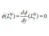
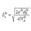
도 22에 n형 실리콘을 사용한 트랜지스터의 소스 측의 밴드 구조를 도시하였다. 도 22를 참조로 하여, 우선, n형 실리콘을 사용한 트랜지스터의 p영역에서의 소스 측의 밴드가 굴곡된 부분의 폭 Ls Si를 산출한다. Ls Si는 억셉터 이온을 갖는 공핍층의 폭과 동일하다. φ(y)는 p-n접합 계면으로부터의 거리 y에서의 전위이며, 원점을 p영역의 진성 준위 EipL Si로 한다. eφF Si는 EipL Si와 페르미 준위 EF Si과의 차이이며 eφF Si=EipL Si―EF Si로 정의한다. 여기서 e는 기본 전하(elementary charge)이다. 밴드가 굴곡된 부분의 폭은 φ(y)의 공간 변화를 반영한다. 수학식 1은 포아송 방정식(Poisson equation)이다.22 shows a band structure on the source side of a transistor using n-type silicon. Referring to FIG. 22, first, the width L s Si of a portion where the band on the source side is bent in the p region of a transistor using n-type silicon is calculated. L s Si is equal to the width of the depletion layer with acceptor ions. φ(y) is a potential at a distance y from the pn junction interface, and the origin is the intrinsic level E ipL Si of the p region. eφ F Si is the difference between E ipL Si and the Fermi level E F Si and is defined as eφ F Si =E ipL Si -E F Si . where e is the elementary charge. The width of the bent portion of the band reflects the spatial change of φ(y).
[수학식 1][Equation 1]
εSi는 유전율, ρ는 전하 밀도이다. p영역의 공핍층에 착안하는 경우에는 ρ는 음 전하를 갖는 억셉터 이온만을 고려하면 좋고, 수학식 2가 된다.ε Si is the permittivity and ρ is the charge density. In the case of focusing on the depletion layer in the p region, only acceptor ions having a negative charge may be considered for ρ, and equation (2) is obtained.
[수학식 2][Equation 2]
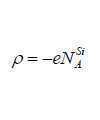
여기서, NA Si는 억셉터 밀도이다. 수학식 2를 수학식 1에 대입하여, 수학식 3으로 나타낸 경계 조건으로 계산하면, 수학식 4가 구해진다.where N A Si is the acceptor density. Equation 4 is obtained by substituting
[수학식 3][Equation 3]
[수학식 4][Equation 4]
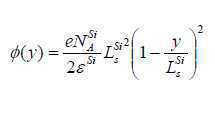
여기서, 수학식 5로 나타낸 경계 조건으로 계산하면, Ls Si가 수학식 6이 구해진다.Here, when calculated with the boundary condition represented by
[수학식 5][Equation 5]
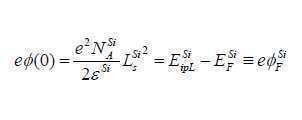
[수학식 6][Equation 6]
한편, Vd를 인가하였을 때의 드레인 측의 밴드가 굴곡된 부분의 폭 Ld Si는 Ls Si의 경우와 같은 계산에 의해 수학식 7이 구해진다.On the other hand, Equation 7 is obtained by the same calculation as in the case of L s Si for the width L d Si of the bent portion of the band on the drain side when V d is applied.
[수학식 7][Equation 7]
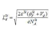
수학식 7로부터 실리콘을 사용한 트랜지스터에서는 Vd에 따라 Ld Si가 증대된다. 즉 Vd에 따라 드레인 측으로부터 공핍층이 넓어지는 것을 알 수 있다. 여기까지 설명한 것이 실리콘을 사용한 트랜지스터의 DIBL이다.From Equation 7, in a transistor using silicon, L d Si increases according to V d . That is, it can be seen that the depletion layer widens from the drain side according to V d . What has been explained so far is DIBL of a transistor using silicon.
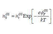
또한, 도 23은 산화물 반도체막을 사용한 트랜지스터의 소스와 드레인 간의 밴드 구조를 도시한 것이다. 도 23을 참조로 하여, 산화물 반도체막을 사용한 트랜지스터의 산화물 반도체 영역에서의 소스 측의 밴드가 굴곡된 부분의 폭 Ls OS 및 드레인 측의 밴드가 굴곡된 부분의 폭 Ld OS를 산출한다. 소스 및 드레인에 사용하는 금속의 일함수 φm과 산화물 반도체의 전자 친화력 χOS가 동일하다(φm=χOS)고 가정하여, 금속-산화물 반도체 간이 오믹 접촉하여 있다고 한다. φ(y)는 소스 측의 금속-산화물 반도체 접합 계면으로부터의 거리 y에서의 전위이며, 원점을 산화물 반도체 영역의 진성 준위 EiL OS로 한다. eφF OS는 EiL OS와 소스 측의 페르미 준위 EF OS 차이이며 eφF OS=EiL OS―EF OS로 정의한다. 이 경우에 산화물 반도체 영역의 밴드가 굴곡된 부분의 폭은 다수 캐리어(majority carrier)인 전자 밀도 nOS(y)에 기인한다고 생각되기 때문에, 전하 밀도 ρ는 수학식 8이 된다.23 shows a band structure between a source and a drain of a transistor using an oxide semiconductor film. Referring to FIG. 23 , the width L s OS of the portion where the band on the source side is bent in the oxide semiconductor region of the transistor using the oxide semiconductor film and the width L d OS of the portion where the band on the drain side is bent are calculated. Assuming that the work function φ m of the metal used for the source and the drain and the electron affinity χ OS of the oxide semiconductor are the same (φ m =χ OS ), it is assumed that the metal-oxide semiconductor is in ohmic contact. φ(y) is a potential at a distance y from the metal-oxide semiconductor junction interface on the source side, and the origin is the intrinsic level E iL OS of the oxide semiconductor region. eφ F OS is the difference between E iL OS and the Fermi level E F OS on the source side, and is defined as eφ F OS =E iL OS ―E F OS . In this case, since the width of the bent portion of the oxide semiconductor region is considered to be due to the electron density n OS (y), which is the majority carrier, the charge density ρ becomes Equation (8).
[수학식 8][Equation 8]
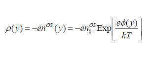
여기서 k는 볼츠만 상수(Boltzmann constant), T는 절대 온도이다. n0 OS는 산화물 반도체의 벌크 영역에서의 전자 밀도이며, 진성 캐리어 밀도 ni OS를 사용하여 수학식 9로 나타내어진다.where k is the Boltzmann constant and T is the absolute temperature. n 0 OS is the electron density in the bulk region of the oxide semiconductor and is represented by Equation 9 using the intrinsic carrier density n i OS .
[수학식 9][Equation 9]
따라서, φ(y)는 수학식 10으로 나타내는 포아송 방정식으로 구해진다.Therefore, φ(y) is obtained by the Poisson equation represented by Equation (10).
[수학식 10][Equation 10]

이것을 수학식 11에 나타내는 경계 조건으로 계산하면, 수학식 12가 구해진다.When this is calculated using the boundary condition shown in
[수학식 11][Equation 11]
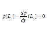
[수학식 12][Equation 12]
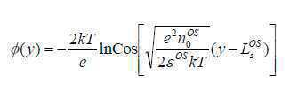
따라서, 수학식 13으로 나타내는 경계 조건으로 계산하면, 수학식 14가 구해진다.Therefore, when calculating with the boundary condition represented by Equation 13, Equation 14 is obtained.
[수학식 13][Equation 13]
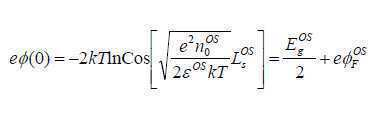
[수학식 14][Equation 14]
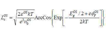
여기서 Eg OS/2+eφF OS>>2kT이기 때문에, 수학식 14는 수학식 15로 나타낸 바와 같이 근사할 수 있다.Here, since E g OS /2 + eφ F OS >> 2kT, equation (14) can be approximated as shown in equation (15).
[수학식 15][Equation 15]
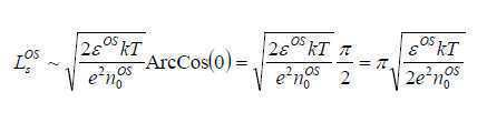
한편, Vd를 인가하였을 때의 Ld OS는 수학식 13의 eφF OS를 eφF OS+eVd로 치환하면 구할 수 있다. 이 경우에도 Eg OS/2+eφF OS+eVd>>2kT이기 때문에, 수학식 16이 된다.On the other hand, L d OS when V d is applied can be obtained by replacing eφ F OS in Equation 13 with eφ F OS + eV d . Also in this case, since E g OS /2 + eφ F OS + eV d >> 2kT, equation (16) is obtained.
[수학식 16][Equation 16]
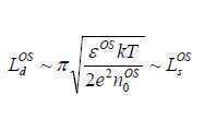
상술한 것으로부터, 산화물 반도체막을 사용한 트랜지스터의 경우에, Ld OS는 Vd에 의존하지 않는 것을 알 수 있다. 그러므로, 산화물 반도체막을 사용한 트랜지스터에 DIBL이 발생하지 않는다고 할 수 있다.From the above, it can be seen that in the case of a transistor using an oxide semiconductor film, L d OS does not depend on V d . Therefore, it can be said that DIBL does not occur in a transistor using an oxide semiconductor film.
또한, 실리콘을 사용한 트랜지스터에서 발생되는 펀치 스루 형상은 게이트의 전계로 인한 공핍층이 채널 영역의 깊은 곳까지 넓어지지 않기 때문에 발생되는 경우도 있다. 이것은 실리콘에 포함되는 소수 캐리어(minority carrier) 밀도가 1×10¹¹개/cm3 정도로 높기 때문이다. 즉 소수 캐리어가 축적됨으로써 게이트의 전계가 깊은 곳까지 침입하지 않아 트랜지스터를 완전한 오프 상태로 할 수 없기 때문에, 오프 전류가 증대된다.In addition, the punch-through shape that occurs in transistors using silicon may occur because the depletion layer due to the electric field of the gate does not extend to the depth of the channel region. This is because the density of minority carriers included in silicon is as high as 1×10 11 /cm 3 . In other words, since minority carriers accumulate, the electric field at the gate does not penetrate deeply and the transistor cannot be turned off completely, so the off-state current increases.
한편, 발명자들의 정력적인 연구의 결과, 산화물 반도체막에 포함되는 소수 캐리어 밀도를 1×10⁻⁹개/cm3 정도로 매우 낮게 할 수 있는 것을 알았다. 즉 산화물 반도체막을 사용한 트랜지스터에서는 소수 캐리어가 거의 축적되지 않고 게이트의 전계가 깊은 곳까지 침입하여, 트랜지스터를 완전한 오프 상태로 하기 쉽기 때문에, 오프 전류를 작게 할 수 있다. 이와 같이 산화물 반도체막을 사용한 트랜지스터에서는 게이트의 전계로 인한 공핍층의 넓어짐이 매우 커진다.On the other hand, as a result of vigorous research by the inventors, it has been found that the minority carrier density contained in the oxide semiconductor film can be made very low, on the order of 1×10 -9 carriers/cm 3 . That is, in a transistor using an oxide semiconductor film, since minority carriers are hardly accumulated and the electric field at the gate penetrates deeply and the transistor is easily turned off completely, the off-state current can be reduced. In a transistor using an oxide semiconductor film as described above, the widening of the depletion layer due to the electric field at the gate becomes very large.
상술한 바와 같이 실리콘을 사용한 트랜지스터에서 일반적으로 알려진 단채널 효과가 산화물 반도체막을 사용한 트랜지스터에서는 실질적으로 없다고 할 수 있다.As described above, it can be said that the short channel effect commonly known in transistors using silicon is substantially absent in transistors using oxide semiconductor films.
따라서, 산화물 반도체막을 사용한 트랜지스터는 채널 길이가 작은 경우에도 스위칭 특성을 얻어지기 쉽다고 할 수 있다.Therefore, it can be said that a transistor using an oxide semiconductor film can easily obtain switching characteristics even when the channel length is small.
또한, 실리콘을 사용한 트랜지스터를 미세화하는 경우, 채널 길이의 축소와 함께 채널 폭도 축소하는 것이 일반적인 일이었다.Also, when miniaturizing transistors using silicon, it has been common to reduce the channel width as well as the channel length.
그러나, 산화물 반도체막을 사용한 트랜지스터에서 채널 길이의 축소와 함께 채널 폭도 축소하면, 임계값 전압이 음 방향으로 이동하는 일이 있었다. 이것도 발명자들의 정력적인 연구의 결과로서 알려진 것의 하나이다.However, in a transistor using an oxide semiconductor film, when the channel width is also reduced along with the reduction in the channel length, the threshold voltage may shift in the negative direction. This is also one of the things known as a result of the inventors' vigorous research.
그러므로, 산화물 반도체막을 사용한 트랜지스터에서 스위칭 특성을 얻기 위해서는 채널 길이가 작은 경우에 채널 폭을 충분히 크게 하는 것이 중요하다고 할 수 있다. 또는, 채널 길이에 대한 채널 폭의 비율을 일정하게 유지하면서 미세화하는 것이 중요하다고 할 수 있다.Therefore, in order to obtain switching characteristics in a transistor using an oxide semiconductor film, it can be said that it is important to sufficiently increase the channel width when the channel length is small. Alternatively, it can be said that it is important to miniaturize while maintaining a constant ratio of channel width to channel length.
여기서, 주목해야 될 일은 산화물 반도체막은 산소 결손으로 인하여 캐리어인 전자를 생성한다는 것이다.Here, it should be noted that the oxide semiconductor film generates electrons as carriers due to oxygen vacancies.
산화물 반도체막으로 전자가 생성되면, 게이트 전압이 제로인 경우에도 트랜지스터가 온 상태가 되는, 소위 노멀리 온(normally-on)의 전기 특성이 되기 쉽다. 그러므로, 산화물 반도체막의 산소 결손을 저감하는 것이 바람직하다.When electrons are generated in the oxide semiconductor film, the transistor tends to be in an on state even when the gate voltage is zero, resulting in so-called normally-on electrical characteristics. Therefore, it is desirable to reduce oxygen vacancies in the oxide semiconductor film.
예를 들어, 산화물 반도체막의 산소 결손을 저감하기 위해서, 산화물 반도체막의 외부로부터 공급되는 산소를 이용하여도 좋다. 외부로부터 산소를 공급하는 방법으로서, 구체적으로는 이온 도핑 처리, 이온 주입 처리, 플라즈마 처리와 같은 산화 처리 등을 수행하면 좋다. 또는, 과잉 산소 함유층을 제공하고 이것으로부터 산화물 반도체막에 산소를 공급하여도 좋다.For example, in order to reduce oxygen vacancies in the oxide semiconductor film, oxygen supplied from the outside of the oxide semiconductor film may be used. As a method of supplying oxygen from the outside, specifically, an ion doping treatment, an ion implantation treatment, an oxidation treatment such as a plasma treatment, or the like may be performed. Alternatively, an excess oxygen-containing layer may be provided and oxygen may be supplied to the oxide semiconductor film therefrom.
이와 같은 방법을 이용하더라도, 산화물 반도체막을 사용한 트랜지스터를 미세화함으로써, 외부로부터 공급되는 산소보다 산화물 반도체막에 생성되는 산소 결손의 비율이 높아질 수 있다. 이것의 원인 중 하나는 미세화에 따라, 산화물 반도체막의 체적에 비하여 표면적이 증대되는 것이다. 이 관점에서 봐도 채널 길이를 작게 한 경우에 채널 폭을 크게 하는 것이 중요하다고 할 수 있다.Even if such a method is used, the proportion of oxygen vacancies generated in the oxide semiconductor film can be higher than that of oxygen supplied from the outside by miniaturizing the transistor using the oxide semiconductor film. One of the causes of this is that the surface area of the oxide semiconductor film increases relative to the volume with miniaturization. Even from this point of view, it can be said that it is important to increase the channel width when the channel length is reduced.
그러나, 채널 폭을 지나치게 크게 하면, 트랜지스터를 미세화한다는 본래의 목적을 달성하지 못한다. 그러므로, 채널 길이와 채널 폭의 비율은 현실적인 범위에서 선택한다. 이러한 관점으로부터 채널 폭을 일정한 범위 이상으로 크게 할 수 없기 때문에, 채널 길이를 제약 없이 작게 하고자 하는 것은 현실적인 일이 아니었을 가능성이 있다.However, if the channel width is too large, the original purpose of miniaturizing the transistor cannot be achieved. Therefore, the ratio of channel length to channel width is selected from a realistic range. From this point of view, since the channel width cannot be increased beyond a certain range, there is a possibility that it was not realistic to make the channel length small without restriction.
그래서, 산화물 반도체막의 외부로부터 공급되는 산소를 유효하게 활용하는 것이 중요하다. 예를 들어, 산화물 반도체막을 사용한 트랜지스터 위에 산소 투과성이 낮은 층을 제공함으로써, 산소의 외방 확산이 억제되어 산소를 유효하게 활용할 수 있게 된다. 따라서, 채널 길이가 작고 채널 폭이 어느 정도 이하의 크기인 경우에도 스위칭 특성을 얻을 수 있다.Therefore, it is important to effectively utilize oxygen supplied from the outside of the oxide semiconductor film. For example, by providing a layer having low oxygen permeability over a transistor using an oxide semiconductor film, outward diffusion of oxygen is suppressed and oxygen can be effectively utilized. Therefore, switching characteristics can be obtained even when the channel length is small and the channel width is less than a certain size.
또한, 산화물 반도체막을 사용한 트랜지스터의 미세화를 진행하면, 산화물 반도체막의 측면에 기생 채널이 형성되는 경우가 있다. 이것도 발명자들의 정력적인 연구에 의해 알려진 것의 하나이다.In addition, when a transistor using an oxide semiconductor film is miniaturized, a parasitic channel may be formed on a side surface of the oxide semiconductor film. This is also one of the things known by the inventors' energetic research.
기생 채널의 영향은 단채널의 트랜지스터에서 현저히 나타날 수 있기 때문에, 단채널 효과와 혼동되기 쉽지만, 엄밀하게 말하면 다른 것이다.Since the effects of parasitic channels can appear prominently in short-channel transistors, they are easily confused with short-channel effects, but strictly speaking, they are different.
기생(寄生) 채널은 트랜지스터의 본래의 채널보다 임계값 전압이 작은 경우가 많다. 그러므로 기생 채널의 영향이 커지면, 마치 트랜지스터의 임계값 전압이 음 방향으로 이동한 것처럼 보인다. 이것은 산화물 반도체막의 측면에서는 캐리어가 생성되기 쉽기 때문이다. 따라서, 산화물 반도체막의 측면에는 다른 표면보다 더 많이 외부로부터 산소를 공급하는 것이 중요하다.The parasitic channel often has a lower threshold voltage than the natural channel of the transistor. Therefore, when the effect of the parasitic channel increases, it looks as if the threshold voltage of the transistor has shifted in the negative direction. This is because carriers are easily generated on the side surface of the oxide semiconductor film. Therefore, it is important to supply more oxygen from the outside to the side surface of the oxide semiconductor film than to other surfaces.
예를 들어, 산화물 반도체막의 측면에 산소 투과성이 낮은 층을 제공하여, 산소 결손이 생성되기 어려운 구조로 하면 좋다. 또한, 산소 투과성이 낮은 층과 적층하여, 과잉 산소 함유층을 산화물 반도체막의 측면에 제공하면 좋다. 이 때, 과잉 산소 함유층을 산화물 반도체막의 측면에 접촉하도록 제공하면 바람직하다.For example, a layer having low oxygen permeability may be provided on the side surface of the oxide semiconductor film to form a structure in which oxygen vacancies are less likely to be generated. Alternatively, a layer containing excess oxygen may be provided on the side surface of the oxide semiconductor film by stacking with a layer having low oxygen permeability. At this time, it is preferable to provide the excess oxygen-containing layer so as to contact the side surface of the oxide semiconductor film.
또한, 산화물 반도체막은 산소 결손 이외에 수소에 의해 캐리어인 전자를 생성하는 것이 알려져 있다. 따라서, 산화물 반도체막 내의 수소도 저감하는 것이 바람직하다.It is also known that the oxide semiconductor film generates electrons as carriers by hydrogen in addition to oxygen vacancies. Therefore, it is desirable to reduce hydrogen in the oxide semiconductor film as well.
소수 캐리어 밀도가 매우 낮고, 또 산소 결손이나 수소 등 캐리어 생성원이 저감된 산화물 반도체막을 사용한 트랜지스터는 오프 전류를 매우 작게 할 수 있다.A transistor using an oxide semiconductor film having a very low minority carrier density and a reduced carrier generation source such as oxygen vacancies or hydrogen can have a very small off-state current.
또한, 산화물 반도체막을 사용한 트랜지스터는 실리콘 등을 사용한 종래의 트랜지스터와 조합하여 사용할 수 있다. 예를 들어, 실리콘을 사용한 트랜지스터나 화합물 반도체를 사용한 트랜지스터 등은 산화물 반도체막을 사용한 트랜지스터와 비교하여 온 특성을 높게 하기 쉽다. 따라서, 온 특성이 요구되는 트랜지스터에는 실리콘을 사용한 트랜지스터나 화합물 반도체를 사용한 트랜지스터 등을 사용하고, 낮은 오프 전류가 요구되는 트랜지스터에는 산화물 반도체막을 사용한 트랜지스터를 적용하여도 좋다. 산화물 반도체막은 스퍼터링법 등의 박막 형성 방법으로 형성할 수 있기 때문에, 다른 반도체 재료와 조합하여 사용할 때의 제약이 적은 것도 특징의 하나이다.Also, a transistor using an oxide semiconductor film can be used in combination with a conventional transistor using silicon or the like. For example, a transistor using silicon, a transistor using a compound semiconductor, or the like tends to have higher on characteristics than a transistor using an oxide semiconductor film. Therefore, a transistor using silicon or a transistor using a compound semiconductor may be used for a transistor requiring on-state characteristics, and a transistor using an oxide semiconductor film may be used for a transistor requiring low off-state current. Since the oxide semiconductor film can be formed by a thin film formation method such as sputtering, one of its characteristics is that there are few restrictions when used in combination with other semiconductor materials.
또한, 실리콘을 사용한 트랜지스터는 실리콘 표면을 수소로 종단(終端)함으로써, 양호한 전기 특성을 얻을 수 있다. 따라서, 실리콘을 사용한 트랜지스터에 대해 수소 공급원이 되는 수소 함유층을 제공하는 것이 바람직하다. 그러나, 상술한 바와 같이 산화물 반도체막을 사용한 트랜지스터에는 수소는 캐리어 생성원이고 전기 특성을 악화시키는 요인이다.Also, a transistor using silicon can obtain good electrical characteristics by terminating the silicon surface with hydrogen. Therefore, it is desirable to provide a hydrogen-containing layer serving as a hydrogen supply source for transistors using silicon. However, as described above, in a transistor using an oxide semiconductor film, hydrogen is a carrier generating source and a factor that deteriorates electrical characteristics.
그러므로, 실리콘을 사용한 트랜지스터와 산화물 반도체막을 사용한 트랜지스터를 조합하여 사용하는 경우, 실리콘을 사용한 트랜지스터 측에 수소 함유층을 제공하고, 산화물 반도체막을 사용한 트랜지스터 측에 수소 투과성이 낮은 층을 제공하면 바람직하다.Therefore, when a transistor using silicon and a transistor using an oxide semiconductor film are used in combination, it is preferable to provide a hydrogen-containing layer on the side of the transistor using silicon and a layer with low hydrogen permeability on the side of the transistor using the oxide semiconductor film.
산화물 반도체막을 사용함으로써, 채널 길이가 작아도 실질적으로 단채널 효과가 발생하지 않고 스위칭 특성이 얻어지는 트랜지스터를 제공할 수 있다.By using an oxide semiconductor film, it is possible to provide a transistor in which switching characteristics are obtained without substantially generating a short-channel effect even when the channel length is small.
또한, 상기 트랜지스터를 적용한 집적도가 높은 반도체 장치를 제공할 수 있다.In addition, a highly integrated semiconductor device to which the transistor is applied can be provided.
도 1(A)는 본 발명의 일 형태에 따른 반도체 장치의 일례를 도시한 상면도이고, 도 1(B) 및 도 1(C)는 그 단면도.
도 2(A)는 본 발명의 일 형태에 따른 반도체 장치의 일례를 도시한 상면도이고, 도 2(B) 및 도 2(C)는 그 단면도.
도 3(A)는 본 발명의 일 형태에 따른 반도체 장치의 일례를 도시한 상면도이고, 도 3(B) 및 도 3(C)는 그 단면도.
도 4(A)는 본 발명의 일 형태에 따른 반도체 장치의 일례를 도시한 상면도이고, 도 4(B) 및 도 4(C)는 그 단면도.
도 5(A) 내지 도 5(C)는 본 발명의 일 형태에 따른 반도체 장치의 제작 방법의 일례를 도시한 단면도.
도 6(A) 내지 도 6(C)는 본 발명의 일 형태에 따른 반도체 장치의 제작 방법의 일례를 도시한 단면도.
도 7(A)는 본 발명의 일 형태에 따른 반도체 장치의 일례를 도시한 상면도이고, 도 7(B) 및 도 7(C)는 그 단면도.
도 8(A) 내지 도 8(D)는 본 발명의 일 형태에 따른 반도체 장치의 제작 방법의 일례를 도시한 단면도.
도 9(A)는 본 발명의 일 형태에 따른 반도체 장치의 일례를 도시한 상면도이고, 도 9(B) 및 도 9(C)는 그 단면도.
도 10(A) 내지 도 10(C)는 본 발명의 일 형태에 따른 반도체 장치의 제작 방법의 일례를 도시한 단면도.
도 11(A) 내지 도 11(C)는 본 발명의 일 형태에 따른 반도체 장치의 제작 방법의 일례를 도시한 단면도.
도 12(A) 내지 도 12(C)는 본 발명의 일 형태에 따른 반도체 장치의 제작 방법의 일례를 도시한 단면도.
도 13(A)는 본 발명의 일 형태에 따른 반도체 장치의 일례를 도시한 상면도이고, 도 13(B) 및 도 13(C)는 그 단면도.
도 14(A) 내지 도 14(C)는 본 발명의 일 형태에 따른 반도체 장치의 제작 방법의 일례를 도시한 단면도.
도 15(A)는 본 발명의 일 형태에 따른 반도체 장치의 일례를 도시한 상면도이고, 도 15(B) 및 도 15(C)는 그 단면도.
도 16(A) 내지 도 16(C)는 본 발명의 일 형태에 따른 반도체 장치의 제작 방법의 일례를 도시한 단면도.
도 17(A)는 본 발명의 일 형태에 따른 반도체 기억 장치의 일례를 도시한 회로도이고, 도 17(B)는 그 전기 특성을 나타낸 도면이고, 도 17(C)는 그 단면도.
도 18(A)는 본 발명의 일 형태에 따른 반도체 기억 장치의 일례를 도시한 회로도이고, 도 18(B)는 그 전기 특성을 나타낸 도면이고, 도 18(C)는 그 단면도.
도 19(A)는 본 발명의 일 형태에 따른 CPU의 구체적인 예를 도시한 블록도이고, 도 19(B) 및 도 19(C)는 그 일부의 회로도.
도 20(A) 내지 도 20(D)는 본 발명의 일 형태에 따른 전자 기기의 일례를 도시한 사시도.
도 21(A) 및 도 21(B)는 n형 실리콘을 사용한 트랜지스터의 소스와 드레인 간의 밴드도.
도 22는 n형 실리콘을 사용한 트랜지스터의 소스 측의 밴드도.
도 23은 산화물 반도체막을 사용한 트랜지스터의 소스와 드레인 간의 밴드도.Fig. 1(A) is a top view showing an example of a semiconductor device according to one embodiment of the present invention, and Figs. 1(B) and 1(C) are cross-sectional views thereof.
Fig. 2(A) is a top view showing an example of a semiconductor device according to one embodiment of the present invention, and Figs. 2(B) and 2(C) are cross-sectional views thereof.
Fig. 3(A) is a top view showing an example of a semiconductor device according to one embodiment of the present invention, and Figs. 3(B) and 3(C) are cross-sectional views thereof.
Fig. 4(A) is a top view showing an example of a semiconductor device according to one embodiment of the present invention, and Figs. 4(B) and 4(C) are cross-sectional views thereof.
5(A) to 5(C) are cross-sectional views showing an example of a method for manufacturing a semiconductor device according to one embodiment of the present invention.
6(A) to 6(C) are cross-sectional views showing an example of a method for manufacturing a semiconductor device according to one embodiment of the present invention.
Fig. 7(A) is a top view showing an example of a semiconductor device according to one embodiment of the present invention, and Figs. 7(B) and 7(C) are cross-sectional views thereof.
8(A) to 8(D) are cross-sectional views showing an example of a method for manufacturing a semiconductor device according to one embodiment of the present invention.
Fig. 9(A) is a top view showing an example of a semiconductor device according to one embodiment of the present invention, and Figs. 9(B) and 9(C) are cross-sectional views thereof.
10(A) to 10(C) are cross-sectional views showing an example of a method for manufacturing a semiconductor device according to one embodiment of the present invention.
11(A) to 11(C) are cross-sectional views showing an example of a method for manufacturing a semiconductor device according to one embodiment of the present invention.
12(A) to 12(C) are cross-sectional views showing an example of a method for manufacturing a semiconductor device according to one embodiment of the present invention.
Fig. 13(A) is a top view showing an example of a semiconductor device according to one embodiment of the present invention, and Figs. 13(B) and 13(C) are cross-sectional views thereof.
14(A) to 14(C) are cross-sectional views showing an example of a method for manufacturing a semiconductor device according to one embodiment of the present invention.
Fig. 15(A) is a top view showing an example of a semiconductor device according to one embodiment of the present invention, and Figs. 15(B) and 15(C) are cross-sectional views thereof.
16(A) to 16(C) are cross-sectional views showing an example of a method for manufacturing a semiconductor device according to one embodiment of the present invention.
Fig. 17(A) is a circuit diagram showing an example of a semiconductor memory device according to one embodiment of the present invention, Fig. 17(B) is a diagram showing its electrical characteristics, and Fig. 17(C) is a cross-sectional view thereof.
Fig. 18(A) is a circuit diagram showing an example of a semiconductor memory device according to one embodiment of the present invention, Fig. 18(B) is a diagram showing its electrical characteristics, and Fig. 18(C) is a cross-sectional view thereof.
Fig. 19(A) is a block diagram showing a specific example of a CPU according to one embodiment of the present invention, and Figs. 19(B) and 19(C) are part circuit diagrams thereof.
20(A) to 20(D) are perspective views showing an example of an electronic device according to one embodiment of the present invention.
21(A) and 21(B) are band diagrams between the source and drain of a transistor using n-type silicon.
Fig. 22 is a band diagram on the source side of a transistor using n-type silicon.
Fig. 23 is a band diagram between the source and drain of a transistor using an oxide semiconductor film;
본 발명의 실시형태에 대해서 도면을 사용하여 자세히 설명한다. 다만, 본 발명은 이하의 설명에 한정되지 않고, 그 형태 및 자세한 사항을 다양하게 변경할 수 있는 것은 당업자라면 용이하게 이해할 수 있다. 또한, 본 발명은 이하에 제시되는 실시형태의 기재 내용에 한정하여 해석되는 것이 아니다. 그리고 도면을 사용하여 발명의 구성을 설명하는 데에 있어서, 같은 것을 가리키는 부호는 다른 도면간에서도 공통적으로 사용한다. 또한, 같은 것을 가리킬 때는 해치 패턴(hatch pattern)을 동일하게 하고 특별히 부호를 붙이지 않은 경우가 있다.EMBODIMENT OF THE INVENTION Embodiment of this invention is described in detail using drawing. However, the present invention is not limited to the following description, and it can be easily understood by those skilled in the art that the form and details can be variously changed. In addition, this invention is limited to the description of embodiment presented below, and is not interpreted. And in explaining the configuration of the invention using the drawings, the same reference numerals are commonly used even between different drawings. In addition, when referring to the same thing, there are cases where the hatch pattern is the same and no special code is attached.
이하에서 본 발명을 설명하는데, 본 명세서에서 사용하는 용어에 대해서 간단하게 설명한다. 우선, 트랜지스터의 소스와 드레인에 대하여, 본 명세서에서는 한쪽을 드레인이라고 부를 때 다른 쪽을 소스라고 한다. 즉, 전위의 고저(高低)에 따라 이들을 구별하지는 않는다. 그래서, 본 명세서에서 소스라고 불리는 부분을 드레인으로 바꾸어 읽을 수도 있다.Hereinafter, the present invention will be described, and the terms used in this specification will be briefly explained. First, regarding the source and drain of a transistor, when one is called a drain in this specification, the other is called a source. That is, they are not distinguished according to the height of the potential. So, in this specification, a portion called a source may be read by changing it to a drain.
또한, 전압은 어느 임의의 전위와 기준 전위(예를 들어, 접지 전위(GND) 또는 소스 전위)의 전위차를 가리키는 경우가 많다. 따라서, 전압을 전위로 바꾸어 말할 수 있다.Also, in many cases, a voltage indicates a potential difference between an arbitrary potential and a reference potential (for example, a ground potential (GND) or a source potential). Therefore, voltage can be converted into potential.
본 명세서에서는 ‘전기적으로 접속된다’라고 표현된 경우에도 현실의 회로에는 물리적인 접속 부분이 없고, 그저 배선이 연장되어 있을 뿐인 경우도 있다.Even when it is expressed as 'electrically connected' in this specification, there are cases where there is no physical connection part in the actual circuit, and the wiring is simply extended.
또한, ‘제 1’, ‘제 2’라고 붙인 서수사(序數詞)는 편의상 사용하는 것이며, 공정 순서 또는 적층 순서를 나타내는 것이 아니다. 또한, 본 명세서에서 발명을 특정하기 위한 사항으로서 고유한 명칭을 나타내는 것이 아니다.In addition, the ordinal suffixes 'first' and 'second' are used for convenience, and do not indicate a process order or stacking order. In addition, it does not represent a unique name as a matter for specifying the invention in this specification.
또한 채널 길이란, 트랜지스터의 소스와 드레인 간 거리를 말한다. 채널 길이가 작을수록 온 저항이 작아지며 고속 동작이 가능한 트랜지스터가 된다. 또한 채널 폭이란, 트랜지스터의 소스 및 드레인의 대향하는 변의 길이를 말한다. 채널 폭이 클수록 온 저항이 작아지며 고속 동작이 가능한 트랜지스터가 된다.Also, the channel length refers to the distance between the source and drain of a transistor. The smaller the channel length, the smaller the on-resistance, resulting in a transistor capable of high-speed operation. The channel width refers to the length of the opposite sides of the source and drain of the transistor. The larger the channel width, the smaller the on-resistance, resulting in a transistor capable of high-speed operation.
(실시형태 1)(Embodiment 1)
본 실시형태에서는 본 발명의 일 형태에 따른 트랜지스터에 대해서 설명한다.In this embodiment, a transistor according to one embodiment of the present invention will be described.
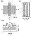
도 1(A)는 본 발명의 일 형태에 따른 트랜지스터의 상면도이다. 도 1(A)에 도시한 일점 쇄선 A1-A2에 대응하는 부분의 단면도를 도 1(B)에 도시하였다. 또한, 도 1(A)에 도시한 일점 쇄선 A3-A4에 대응하는 부분의 단면도를 도 1(C)에 도시하였다. 또한 설명하기 쉽게 하기 위해서, 도 1(A)에서는 하지 절연막(base insulating film, 102) 등을 생략하였다.1(A) is a top view of a transistor according to one embodiment of the present invention. A cross-sectional view of a portion corresponding to the dashed-dotted line A1-A2 shown in FIG. 1(A) is shown in FIG. 1(B). Further, a cross-sectional view of a portion corresponding to the dashed-dotted line A3-A4 shown in FIG. 1(A) is shown in FIG. 1(C). Also, for ease of explanation, a
도 1(A)에 트랜지스터의 채널 길이(L) 및 채널 폭(W)을 도시하였다. 또한, 트랜지스터의 채널 영역은 산화물 반도체막(106)에서의 게이트 전극(104)과 중첩되는 영역이다. 그리고 산화물 반도체막(106)의 2개의 측면의 적어도 일부는 게이트 전극(104)과 중첩된다.1(A) shows the channel length (L) and channel width (W) of the transistor. Also, the channel region of the transistor is a region overlapping the
도 1(A)에 도시한 트랜지스터는 채널 길이가 5nm 이상 60nm 미만, 또 채널 폭이 5nm 이상 200nm 미만이다.The transistor shown in Fig. 1(A) has a channel length of 5 nm or more and less than 60 nm, and a channel width of 5 nm or more and less than 200 nm.
또한, 도 1(A)에 도시한 트랜지스터는 채널 폭이 채널 길이의 0.5배 이상 10배 이하이다.In the transistor shown in Fig. 1(A), the channel width is 0.5 times or more and 10 times or less the channel length.
도 1(B)는 기판(100) 위에 제공된 하지 절연막(102)과, 하지 절연막(102) 위에 제공된 산화물 반도체막(106)과, 산화물 반도체막(106) 위에 제공된 게이트 절연막(112)과, 게이트 절연막(112) 위에 있으며 산화물 반도체막(106)과 중첩되어 제공된 게이트 전극(104)을 갖는 트랜지스터의 단면 구조를 도시한 것이다.1(B) shows a
또한, 도 1(B)에는 산화물 반도체막(106) 및 게이트 전극(104) 위에 제공되며, 산화물 반도체막(106)에 도달하는 개구부들을 갖는 층간 절연막(118)과, 층간 절연막(118)의 개구부들을 통하여 산화물 반도체막(106)과 접촉하도록 제공된 배선(136)을 도시하였다.1(B), an
산화물 반도체막(106)의 재료로서는 예를 들어, In-M-Zn-O계 재료를 사용하면 좋다. 여기서, 금속 원소 M은 산소와의 결합 에너지가 In 및 Zn보다 높은 원소이다. 또는, In-M-Zn-O계 재료로부터 산소가 이탈되는 것을 억제하는 기능을 갖는 원소이다. 금속 원소 M의 작용에 의하여 산화물 반도체막의 산소 결손의 발생이 어느 정도 억제된다. 그러므로 산소 결손으로 인한 트랜지스터의 전기 특성의 변동을 저감할 수 있어, 신뢰성이 높은 트랜지스터를 얻을 수 있다.As the material of the
금속 원소 M은 구체적으로는 Al, Sc, Ti, V, Cr, Mn, Fe, Co, Ni, Ga, Y, Zr, Nb, Mo, Sn, La, Ce, Pr, Nd, Sm, Eu, Gd, Tb, Dy, Ho, Er, Tm, Yb, Lu, Hf, Ta, 또는 W로 하면 좋고, 바람직하게는 Al, Ti, Ga, Y, Zr, Ce, 또는 Hf로 한다. 금속 원소 M은 상술한 원소 중에서 1종류 또는 2종류 이상을 선택하면 좋다. 또한, 금속 원소 M 대신에 Si 또는 Ge를 사용하여도 좋다.The metal element M is specifically Al, Sc, Ti, V, Cr, Mn, Fe, Co, Ni, Ga, Y, Zr, Nb, Mo, Sn, La, Ce, Pr, Nd, Sm, Eu, Gd , Tb, Dy, Ho, Er, Tm, Yb, Lu, Hf, Ta, or W, preferably Al, Ti, Ga, Y, Zr, Ce, or Hf. The metal element M may be selected from one type or two or more types from among the above-mentioned elements. Alternatively, Si or Ge may be used instead of the metal element M.
다만, 산화물 반도체막(106)에 함유되는 금속 원소 M의 작용만으로는 산화물 반도체막(106)의 산소 결손의 생성을 완전히 억제할 수는 없다. 그러므로 하지 절연막(102) 및 게이트 절연막(112) 중 적어도 한쪽으로부터 산소를 공급하는 것이 중요하다.However, generation of oxygen vacancies in the
또한, 산화물 반도체막(106) 내의 수소 농도를 2×10²⁰atoms/cm3 이하, 바람직하게는 5×10¹⁹atoms/cm3 이하, 더 바람직하게는 1×10¹⁹atoms/cm3 이하로 한다. 이것은 산화물 반도체막(106)에 함유되는 수소가 의도하지 않은 캐리어를 생성하는 경우가 있기 때문이다. 생성된 캐리어는 트랜지스터의 전기 특성을 변동시키는 요인이 된다.Further, the hydrogen concentration in the
산화물 반도체막(106)은 단결정, 다결정(폴리크리스탈이라고도 함), 또는 비정질 등의 상태를 취한다.The
바람직하게는, 산화물 반도체막(106)은 CAAC-OS(C Axis Aligned Crystalline Oxide Semiconductor)막으로 한다.Preferably, the
CAAC-OS막은 완전한 단결정이 아니고, 완전한 비정질도 아니다. CAAC-OS막은 비정질상에 결정부를 갖는 결정-비정질 혼상 구조의 산화물 반도체막이다. 또한, 상기 결정부는 하나의 변이 100nm 미만인 입방체 내에 들어가는 크기인 경우가 많다. 또한, 투과형 전자 현미경(TEM: Transmission Electron Microscope)에 의한 관찰상에서는 CAAC-OS막에 포함되는 비정질부와 결정부의 경계는 명확하지 않다. 그리고, TEM에 의한 관찰에서는 CAAC-OS막에는 입계(그레인 바운더리(grain boundary)라고도 함)가 확인되지 않는다. 그래서, CAAC-OS막은 입계에 기인한 캐리어 이동도의 저하가 억제된다.The CAAC-OS film is neither completely single crystal nor completely amorphous. The CAAC-OS film is an oxide semiconductor film having a crystal-amorphous mixed phase structure having crystal parts in an amorphous phase. In many cases, the crystal portion has a size that fits within a cube with one side less than 100 nm. In addition, the boundary between the amorphous part and the crystalline part included in the CAAC-OS film is not clear in observation with a transmission electron microscope (TEM). Further, in observation by TEM, grain boundaries (also referred to as grain boundaries) are not observed in the CAAC-OS film. Therefore, in the CAAC-OS film, a decrease in carrier mobility due to grain boundaries is suppressed.
CAAC-OS막에 포함되는 결정부는 c축이 CAAC-OS막의 피형성면(CAAC-OS막이 형성되는 면) 또는 상면에 수직인 방향으로 정렬되고, 또 ab면에 수직인 방향으로부터 보아 삼각형 또는 육각형의 원자 배열을 갖고, c축에 수직인 방향으로부터 보아 금속 원자가 층상 또는 금속 원자와 산소 원자가 층상으로 배열되어 있다. 또한, 상이한 결정부 사이에서 a축 및 b축의 방향이 각각 상이하여도 좋다. 본 명세서에서 단순히 수직이라고 기재된 경우에는, 85° 이상 95° 이하의 범위도 포함되는 것으로 한다.The crystal part included in the CAAC-OS film has the c-axis aligned in a direction perpendicular to the formed surface (the surface on which the CAAC-OS film is formed) or the upper surface of the CAAC-OS film, and has a triangular or hexagonal shape when viewed from a direction perpendicular to the ab-plane. It has an atomic arrangement of , and metal atoms are arranged in layers or metal atoms and oxygen atoms are arranged in layers when viewed from a direction perpendicular to the c-axis. Further, the a-axis and b-axis directions may be different between different crystal parts. In the case where it is simply described as vertical in this specification, it is assumed that the range of 85° or more and 95° or less is also included.
또한, CAAC-OS막에서 결정부의 분포가 균일하지 않아도 좋다. 예를 들어, CAAC-OS막의 형성 과정에서 산화물 반도체막(106)의 상면 측으로부터 결정 성장시키는 경우에는, 산화물 반도체막의 피형성면 측보다 상면 측에서 결정부가 차지하는 비율이 높아지는 경우가 있다. 또한, CAAC-OS막에 불순물을 첨가함으로써 상기 불순물 첨가 영역에서 결정부가 비정질화되는 경우도 있다.Further, the distribution of crystal parts in the CAAC-OS film does not have to be uniform. For example, in the case of crystal growth from the upper surface side of the
CAAC-OS막에 포함되는 결정부의 c축은 CAAC-OS막의 피형성면의 법선 벡터 또는 상면의 법선 벡터에 평행한 방향으로 정렬되기 때문에, CAAC-OS막의 형상(CAAC-OS막의 피형성면의 단면 형상 또는 상면의 단면 형상)에 따라서는 서로 상이한 방향을 향하는 경우가 있다. 또한, 결정부의 c축의 방향은 CAAC-OS막의 피형성면의 법선 벡터 또는 상면의 법선 벡터에 평행한 방향이 된다. 성막(成膜)함으로써 또는 성막 후에 열처리 등의 결정화 처리를 수행함으로써, 결정부가 형성된다.Since the c-axis of the crystal part included in the CAAC-OS film is aligned in a direction parallel to the normal vector of the formed surface of the CAAC-OS film or the normal vector of the upper surface, the shape of the CAAC-OS film (cross section of the formed surface of the CAAC-OS film) Depending on the shape or cross-sectional shape of the upper surface), there are cases in which they are oriented in different directions. Further, the direction of the c-axis of the crystal part is a direction parallel to the normal vector of the formed surface of the CAAC-OS film or the normal vector of the upper surface. A crystal portion is formed by forming a film or by performing a crystallization process such as heat treatment after film formation.
CAAC-OS막을 사용한 트랜지스터는 가시광이나 자외광의 조사로 인한 전기 특성의 변동이 작다. 따라서, 상기 트랜지스터는 신뢰성이 높다.A transistor using a CAAC-OS film has little change in electrical characteristics due to irradiation with visible light or ultraviolet light. Therefore, the transistor has high reliability.
또한, 산화물 반도체막(106)은 영역(106a) 및 영역(106b)을 갖는다. 영역(106a)은 채널 영역으로서 기능하고, 영역(106b)은 소스 영역 및 드레인 영역으로서 기능한다. 따라서, 영역(106b)은 반도체가 아니라 도체라고 불러야 하는 경우가 있다. 그러므로 편의상 산화물 반도체막(106)이라고 기재한 경우에도 영역(106b)을 제외하고 영역(106a)만을 가리키는 경우가 있다.In addition, the
영역(106b)은 영역(106a)보다 저항이 낮은 영역이다. 영역(106b)은 산화물 반도체막의 저항을 낮추는 작용이 있는 불순물을 함유한 영역이다. 산화물 반도체막의 저항을 낮추는 작용이 있는 불순물은 예를 들어, 헬륨, 붕소, 질소, 불소, 네온, 알루미늄, 인, 아르곤, 비소, 크립톤, 인듐, 주석, 안티몬, 및 크세논을 들 수 있다.
산화물 반도체막(106)에서의 영역(106a)은 밴드갭이 2.8eV 내지 3.2eV 정도이고, 소수 캐리어 밀도가 10-9개/cm3 정도로 매우 낮고, 다수 캐리어는 트랜지스터의 소스로부터만 흘러온다.The
산화물 반도체막(106)은 실리콘에 비해 밴드갭이 1eV 내지 2eV 정도 크다. 그러므로 산화물 반도체막(106)을 사용한 트랜지스터는 충돌 이온화(impact ionization)가 발생하기 어려워, 애벌란시 항복(avalanche breakdown)이 일어나기 어렵다. 즉 상기 트랜지스터는 핫 캐리어로 인한 열화가 일어나기 어렵다고 할 수 있다.The
또한, 영역(106a)은 불순물 농도가 낮고 산소 결손이 적다. 그러므로 상기 트랜지스터는 산화물 반도체막(106)의 두께가 두꺼운 경우(예를 들어 15nm 이상 100nm 미만)에도 게이트 전극(104)의 전계에 의하여 영역(106a)을 완전한 공핍 상태로 할 수 있다. 따라서, 상기 트랜지스터는 펀치 스루 형상으로 인하여 임계값 전압이 음 방향으로 이동하는 일이 없고, 또 예를 들어 채널 길이가 3μm일 때, 채널 폭 1μm당 오프 전류를 실온에서 10-21A 미만, 또는 10-24A 미만으로 할 수 있다.Further, the
산소 결손이 적은 산화물 반도체막은 전자 스핀 공명(ESR: Electron Spin Resonance)에 의하여 측정한 경우에, 산소 결손에 기인한 신호를 나타내지 않는 산화물 반도체막이다. 구체적으로는 산소 결손에 기인한 스핀 밀도가 5×10¹⁶spins/cm3 미만인 산화물 반도체막이다. 또한, 산화물 반도체막이 산소 결손을 가지면, ESR에서 측정한 경우에, 1.93 근방의 g 값에서 대칭성을 갖는 신호를 나타낸다.An oxide semiconductor film with few oxygen vacancies is an oxide semiconductor film that does not show a signal due to oxygen vacancies when measured by electron spin resonance (ESR). Specifically, it is an oxide semiconductor film whose spin density due to oxygen vacancies is less than 5×10 16 spins/cm 3 . Further, when the oxide semiconductor film has oxygen vacancies, a signal having symmetry at a g value of around 1.93 is exhibited when measured by ESR.
하지 절연막(102)은 충분한 평탄성을 갖는 것이 바람직하다. 구체적으로는, 평균 면 거칠기(Ra)를 1nm 이하, 바람직하게는 0.3nm 이하, 더 바람직하게는 0.1nm 이하로 한다. Ra를 상술한 값 이하로 함으로써, 결정화도가 높은 산화물 반도체막(106)을 형성할 수 있다. 또한, 하지 절연막(102)과 산화물 반도체막(106)의 계면의 요철이 작아짐으로써 계면 산란의 영향을 작게 할 수 있다. 또한 Ra란, JIS B 0601:2001(ISO4287: 1997)에 정의되어 있는 산술 평균 거칠기를 곡면에 적용할 수 있도록 3차원으로 확장한 것이며, ‘기준면으로부터 지정면까지의 편차의 절대값을 평균한 값’으로 표현할 수 있고, 수학식 17로 정의된다.The underlying
[수학식 17][Equation 17]
여기서 지정면이란, 거칠기 계측의 대상이 되는 면이며, 좌표(x1, y1, f(x1, y1)), (x1, y2, f(x1, y2)), (x2, y1, f(x2, y1)), (x2, y2, f(x2, y2))의 4점을 연결하여 이루어진 사각형의 영역으로 하고, 지정면을 xy 평면에 투영한 직사각형의 면적을 S0, 기준면의 높이(지정면의 평균 높이)를 Z0으로 한다. Ra는 원자간력 현미경(AFM: Atomic Force Microscope)으로 평가할 수 있다.Here, the designated surface is the surface to be measured for roughness, and the coordinates (x 1 , y 1 , f(x 1 , y 1 )), (x 1 , y 2 , f(x 1 , y 2 )), (x 2 , y 1 , f(x 2 , y 1 )), (x 2 , y 2 , f(x 2 , y 2 )) is a rectangular area formed by connecting 4 points, and the specified surface is projected onto the xy plane The area of one rectangle is S 0 , and the height of the reference plane (average height of the designated plane) is Z 0 . Ra can be evaluated with an atomic force microscope (AFM).
하지 절연막(102)은 과잉 산소를 함유한 절연막이면 바람직하다.The base
과잉 산소를 함유한 절연막이란, TDS(Thermal Desorption Spectroscopy: 승온 이탈 가스 분광법) 분석에 의하여 방출되는 산소가 산소 원자로 환산하여 1×10¹⁸atoms/cm3 이상, 1×10¹⁹atoms/cm3 이상, 또는 1×10²⁰atoms/cm3 이상인 절연막을 가리킨다.An insulating film containing excess oxygen means that the oxygen released by TDS (Thermal Desorption Spectroscopy: Elevated Desorption Gas Spectroscopy) analysis is converted into oxygen atoms and is 1×10 18 atoms/cm 3 or more, 1×10 19 atoms/cm 3 or more, Or an insulating film of 1×10 20 atoms/cm 3 or more.
여기서, TDS 분석을 이용하여 산소의 방출량을 측정하는 방법에 대하여 이하에서 설명한다.Here, a method of measuring the amount of oxygen released using TDS analysis will be described below.
TDS 분석을 하였을 때의 기체의 총 방출량은 방출 가스의 이온 강도의 적분값에 비례한다. 그리고, 이 적분값과 표준 시료의 비교에 의하여 기체의 총 방출량을 계산할 수 있다.When the TDS analysis is performed, the total emission amount of the gas is proportional to the integral value of the ionic strength of the emission gas. In addition, the total emission amount of gas can be calculated by comparing the integral value with the standard sample.
예를 들어, 절연막의 산소 분자의 방출량(NO2)은 표준 시료인 소정의 밀도의 수소를 함유한 실리콘 웨이퍼의 TDS 분석을 한 결과, 및 절연막의 TDS 분석을 한 결과로부터, 수학식 18을 사용해서 계산할 수 있다. 여기서, TDS 분석에 의하여 얻어지는 질량수가 32로 검출되는 가스 모두가 산소 분자에서 유래한 것이라고 가정한다. 질량수가 32인 것으로서 산소 이외에 CH3OH가 있지만, 존재할 가능성이 낮은 것으로 하여 여기서는 고려하지 않는다. 또한, 산소 원자의 동위체인 질량수가 17인 산소 원자 및 질량수가 18인 산소 원자를 함유한 산소 분자에 관해서도 자연계에서의 존재 비율이 매우 미량이기 때문에 고려하지 않는다.For example, the amount of oxygen molecule emitted from the insulating film (N O2 ) is determined by using Equation 18 from the results of TDS analysis of a silicon wafer containing a predetermined density of hydrogen, which is a standard sample, and the result of TDS analysis of the insulating film. can be calculated by Here, it is assumed that all gases whose mass number is 32 obtained by TDS analysis are derived from oxygen molecules. It has a mass number of 32 and there is CH 3 OH in addition to oxygen, but it is not considered here because it is unlikely to exist. Also, an oxygen atom with a mass number of 17, which is an isotope of an oxygen atom, and an oxygen molecule containing an oxygen atom with a mass number of 18 are not considered because their existence ratio in the natural world is very small.
[수학식 18][Equation 18]
NH2는 표준 시료로부터 이탈된 수소 분자를 밀도로 환산한 값이다. SH2는 표준 시료를 TDS 분석하였을 때의 이온 강도의 적분값이다. 여기서 표준 시료의 기준값을 NH2/SH2로 한다. SO2는 절연막을 TDS 분석하였을 때의 이온 강도의 적분값이다. α는 TDS 분석에서의 이온 강도에 영향을 미치는 계수이다. 수학식 18의 상세한 사항에 관해서는, 일본국 특개평6-275697호 공보를 참조한다. 또한, 상기 절연막의 산소의 방출량은 승온 이탈 분석 장치 EMD-WA1000S/W(ESCO Ltd., 제조)를 이용하며, 표준 시료로서 1×10¹⁶atoms/cm2의 수소 원자를 함유한 실리콘 웨이퍼를 사용하여 측정하였다.N H2 is a value obtained by converting hydrogen molecules released from a standard sample into a density. S H2 is an integral value of ionic strength when a standard sample is subjected to TDS analysis. Here, the reference value of the standard sample is N H2 /S H2 . S O2 is an integral value of ionic strength when the insulating film is subjected to TDS analysis. α is a coefficient affecting the ionic strength in TDS analysis. For details of Equation 18, refer to Japanese Patent Laid-Open No. 6-275697. In addition, the oxygen emission amount of the insulating film is measured using a temperature rise and departure analyzer EMD-WA1000S/W (manufactured by ESCO Ltd.), and a silicon wafer containing hydrogen atoms of 1×10 16 atoms/cm 2 is used as a standard sample. was measured.
또한, TDS 분석에 있어서 산소의 일부는 산소 원자로서 검출된다. 산소 분자와 산소 원자의 비율은 산소 분자의 이온화율로부터 산출할 수 있다. 또한, 상기 α는 산소 분자의 이온화율을 포함하기 때문에, 산소 분자의 방출량을 평가함으로써 산소 원자의 방출량도 어림잡을 수 있다.Also, in the TDS analysis, a part of oxygen is detected as an oxygen atom. The ratio of oxygen molecules to oxygen atoms can be calculated from the ionization rate of oxygen molecules. In addition, since α includes the ionization rate of oxygen molecules, the amount of oxygen atoms released can also be estimated by evaluating the amount of oxygen molecules released.
또한, NO2는 산소 분자의 방출량이다. 산소 원자로 환산하였을 때의 산소의 방출량은 산소 분자의 산소의 방출량의 2배가 된다.Also, N O2 is the released amount of oxygen molecules. The amount of oxygen released when converted into oxygen atoms is twice the amount of oxygen released from oxygen molecules.
또는, 과잉 산소를 함유한 절연막은 과산화 라디칼을 함유한 절연막이라도 좋다. 구체적으로는 과산화 라디칼에 기인한 스핀 밀도가 5×10¹⁷spins/cm3 이상인 절연막이다. 또한, 과산화 라디칼을 함유한 절연막은 ESR에서 측정한 경우에, 2.01 근방의 g 값에서 비대칭성을 갖는 신호를 나타내는 절연막이다.Alternatively, the insulating film containing excess oxygen may be an insulating film containing peroxide radicals. Specifically, it is an insulating film having a spin density of 5×10 17 spins/cm 3 or higher due to peroxide radicals. In addition, an insulating film containing peroxide radicals is an insulating film that exhibits a signal having an asymmetry at a g value of around 2.01 when measured by ESR.
또는, 과잉 산소를 함유한 절연막은 산소가 과잉으로 함유된 산화 실리콘(SiOX(X>2))이어도 좋다. 산소가 과잉으로 함유된 산화 실리콘(SiOX(X>2))은 단위 체적당 실리콘 원자수의 2배보다 많은 산소 원자를 함유한 것이다. 단위 체적당 실리콘 원자수 및 산소 원자수는 러더퍼드 후방 산란법(Rutherford Backscattering Spectrometry)에 의하여 측정한 값이다.Alternatively, the insulating film containing excess oxygen may be silicon oxide (SiO X (X>2)) containing excess oxygen. Oxygenated silicon oxide (SiO X (X>2)) is one containing more than twice the number of silicon atoms per unit volume of oxygen atoms. The number of silicon atoms and the number of oxygen atoms per unit volume are values measured by Rutherford Backscattering Spectrometry.
하지 절연막(102)은 산화 알루미늄, 질화 알루미늄, 산화 마그네슘, 산화 실리콘, 산화질화 실리콘, 산화 게르마늄, 산화 이트륨, 산화 지르코늄, 산화 란탄, 산화 네오디뮴, 산화 하프늄, 및 산화 탄탈 중에서 1종류 이상을 함유한 재료를 선택하여 단층으로 또는 적층하여 형성하면 좋다. 또한, 상술한 단층 또는 적층에 더하여 질화산화 실리콘, 질화 실리콘을 적층하여도 좋다.The base
산화질화 실리콘이란, 그 조성이 질소보다 산소의 함유량이 많은 것을 가리키고, 질화산화 실리콘이란, 그 조성이 산소보다 질소의 함유량이 많은 것을 가리킨다.Silicon oxynitride refers to a composition containing more oxygen than nitrogen, and silicon nitride oxide refers to a composition containing more nitrogen than oxygen.
또한, 게이트 절연막(112)은 과잉 산소를 함유한 절연막이면 바람직하다.In addition, it is preferable that the
게이트 절연막(112)은 산화 알루미늄, 산화 마그네슘, 산화 실리콘, 산화질화 실리콘, 질화산화 실리콘, 질화 실리콘, 산화 게르마늄, 산화 이트륨, 산화 지르코늄, 산화 란탄, 산화 네오디뮴, 산화 하프늄, 및 산화 탄탈 중에서 1종류 이상을 함유한 재료를 선택하여 단층으로 또는 적층하여 형성하면 좋다.The
하지 절연막(102) 및 게이트 절연막(112) 중 적어도 한쪽에 함유되는 과잉 산소는 재료의 화학양론적 조성보다 많이 함유되는 산소이다. 따라서, 과잉 산소는 열 등의 에너지를 받으면 방출된다는 성질을 갖는다. 과잉 산소란, 화학양론적 조성에 비해 과잉으로 함유되어 있는 것이기 때문에, 방출되어 소실되어도 막질은 저하되지 않는다.Excess oxygen contained in at least one of the
예를 들어, 산화물 반도체막(106)의 산소 결손은 하지 절연막(102) 및 게이트 절연막(112) 중 한쪽으로부터 공급되는 산소에 의해 저감할 수 있다. 즉 산화물 반도체막(106)의 산소 결손이 저감됨으로써, 트랜지스터의 임계값 전압이 음 방향으로 이동하는 것을 억제할 수 있다. 그러므로 하지 절연막 및 게이트 절연막 중 적어도 한쪽으로서, 과잉 산소를 함유한 절연막을 사용하면 좋다.For example, oxygen vacancies in the
또한 산화물 반도체막(106)을 하지 절연막(102)과 게이트 절연막(112)에 끼워 열처리함으로써, 하지 절연막(102)으로부터 방출시킨 산소를 산화물 반도체막(106)으로 효율적으로 공급할 수 있다. 또한, 상기 열처리를 250℃ 이상 550℃ 이하의 온도로 수행하면, 산화물 반도체막(106)에 산소를 공급함과 함께 산화물 반도체막(106), 하지 절연막(102) 및 게이트 절연막(112)의 수소 농도를 저감할 수 있다.Further, by heat treating the
다만 상기 열처리로 인하여, 하지 절연막(102) 및 게이트 절연막(112) 중 한쪽에 함유된 과잉 산소가 소실될 수 있다. 트랜지스터의 전기 특성의 변동을 저감한다는 관점에서는 열처리 후에도 하지 절연막(102) 및 게이트 절연막(112) 중 한쪽은 과잉 산소를 함유하는 것이 바람직하다.However, due to the heat treatment, excess oxygen contained in one of the underlying insulating
기판(100)에 큰 제한은 없지만, 적어도 나중의 열처리에 견딜 수 있을 정도의 내열성을 가질 필요가 있다. 예를 들어, 유리 기판, 세라믹스 기판, 석영 기판, 사파이어 기판 등을 기판(100)으로서 사용하여도 좋다. 또한, 실리콘이나 탄소화 실리콘 등을 사용한 단결정 반도체 기판이나 다결정 반도체 기판, 실리콘게르마늄 등을 사용한 화합물 반도체 기판, SOI(Silicon On Insulator) 기판 등을 적용할 수도 있으며, 상술한 기판 위에 반도체 소자가 제공된 것을 기판(100)으로서 사용하여도 좋다.The
또한, 기판(100)으로서 제 5 세대(1000mm×1200mm 또는 1300mm×1500mm), 제 6 세대(1500mm×1800mm), 제 7 세대(1870mm×2200mm), 제 8 세대(2200mm×2500mm), 제 9 세대(2400mm×2800mm), 제 10 세대(2880mm×3130mm) 등 대형 유리 기판을 사용하는 경우에는, 반도체 장치의 제작 공정에서 열처리 등으로 인하여 기판(100)이 수축됨으로써 미세한 가공이 어려워지는 경우가 있다. 따라서, 상술한 바와 같은 대형 유리 기판을 기판(100)으로서 사용하는 경우에는, 열처리로 인하여 그다지 수축되지 않는 것을 사용하는 것이 바람직하다. 예를 들어 기판(100)으로서 400℃, 바람직하게는 450℃, 더 바람직하게는 500℃의 온도로 1시간 동안 열처리한 후의 수축량이 10ppm 이하, 바람직하게는 5ppm 이하, 더 바람직하게는 3ppm 이하인 대형 유리 기판을 사용하면 좋다.In addition, as the
또한, 기판(100)으로서 가요성 기판을 사용하여도 좋다. 또한, 가요성 기판 위에 트랜지스터를 제작하는 방법으로서, 비가요성 기판 위에 트랜지스터를 제작한 후에 트랜지스터를 박리하고, 가요성 기판인 기판(100)으로 전치(轉置)하는 방법도 있다. 이 경우에는 비가요성 기판과 트랜지스터 사이에 박리층을 제공하면 좋다.Alternatively, a flexible substrate may be used as the
게이트 전극(104)은 Al, Ti, Cr, Co, Ni, Cu, Y, Zr, Mo, Ag, Ta, 및 W 중 1종류 이상을 함유한 단체(單體), 질화물, 산화물, 또는 합금을 단층으로 또는 적층하여 형성하면 좋다.The
층간 절연막(118)은 산화 알루미늄, 질화 알루미늄, 산화 마그네슘, 산화 실리콘, 산화질화 실리콘, 질화산화 실리콘, 질화 실리콘, 산화 게르마늄, 산화 이트륨, 산화 지르코늄, 산화 란탄, 산화 네오디뮴, 산화 하프늄, 및 산화 탄탈 중에서 1종류 이상을 함유한 재료를 선택하여 단층으로 또는 적층하여 형성하면 좋다.The
또한, 층간 절연막(118)은 비유전율이 낮고, 또 충분한 두께를 갖는 것이 바람직하다. 예를 들어, 비유전율이 3.8 정도인 산화 실리콘막을 사용하여 200nm 이상 1000nm 이하의 두께로 하면 좋다. 층간 절연막(118)의 상면은 대기 성분 등의 영향으로 약간의 고정 전하를 가지며, 그 영향으로 인하여 트랜지스터의 임계값 전압이 변동될 경우가 있다. 그러므로 층간 절연막(118)은 상면에 생기는 전하의 영향이 충분히 작게 되도록 비유전율 및 두께를 설정하는 것이 바람직하다. 같은 이유로 층간 절연막(118) 위에 폴리이미드 수지, 아크릴 수지, 에폭시 수지, 실리콘(silicone) 수지 등의 수지막을 형성함으로써, 층간 절연막(118)의 상면에 생기는 전하의 영향을 저감하여도 좋다.In addition, the
배선(136)은 Al, Ti, Cr, Co, Ni, Cu, Y, Zr, Mo, Ag, Ta, 및 W 중에서 1종류 이상을 함유한 단체, 질화물, 산화물, 또는 합금을 단층으로 또는 적층하여 형성하면 좋다.The
이어서, 도 1(A) 내지 도 1(C)에 도시한 트랜지스터와 다른 구조의 트랜지스터에 대하여 도 2(A) 내지 도 2(C)를 사용하여 설명한다.Next, transistors having structures different from those shown in Figs. 1(A) to 1(C) will be described using Figs. 2(A) to 2(C).
도 2(A)는 본 발명의 일 형태에 따른 트랜지스터의 상면도이다. 도 2(A)에 도시한 일점 쇄선 B1-B2에 대응하는 부분의 단면도를 도 2(B)에 도시하였다. 또한, 도 2(A)에 도시한 일점 쇄선 B3-B4에 대응하는 부분의 단면도를 도 2(C)에 도시하였다. 또한, 설명하기 쉽게 하기 위해서, 도 2(A)에서는 하지 절연막(102) 등을 생략하였다.2(A) is a top view of a transistor according to one embodiment of the present invention. 2(B) is a cross-sectional view of a portion corresponding to the dashed-dotted line B1-B2 shown in FIG. 2(A). Further, a cross-sectional view of a portion corresponding to the dashed-dotted line B3-B4 shown in FIG. 2(A) is shown in FIG. 2(C). Note that, for ease of explanation, the underlying insulating
도 2(A)에 트랜지스터의 채널 길이(L) 및 채널 폭(W)을 도시하였다. 또한, 트랜지스터의 채널 영역은 산화물 반도체막(106)에서의 게이트 전극(104)과 중첩되는 영역이다. 그리고 산화물 반도체막(106)의 2개의 측면의 적어도 일부는 게이트 전극(104)과 중첩된다.2(A) shows the channel length (L) and channel width (W) of the transistor. Also, the channel region of the transistor is a region overlapping the
도 2(A)에 도시한 트랜지스터는 채널 길이가 5nm 이상 60nm 미만, 또 채널 폭이 5nm 이상 200nm 미만이다.The transistor shown in Fig. 2(A) has a channel length of 5 nm or more and less than 60 nm, and a channel width of 5 nm or more and less than 200 nm.
또한, 도 2(A)에 도시한 트랜지스터는 채널 폭이 채널 길이의 0.5배 이상 10배 이하이다.In the transistor shown in Fig. 2(A), the channel width is 0.5 times or more and 10 times or less the channel length.
도 2(B)는 기판(100) 위에 제공된 하지 절연막(102)과, 하지 절연막(102) 위에 제공된 산화물 반도체막(106)과, 산화물 반도체막(106) 위에 제공된 게이트 절연막(112)과, 게이트 절연막(112) 위에 있으며 산화물 반도체막(106)과 중첩되어 제공된 게이트 전극(104)과, 하지 절연막(102), 산화물 반도체막(106), 및 게이트 전극(104) 위에 제공되며, 산화물 반도체막(106)에 도달하는 개구부들을 갖는 배리어막(108)을 갖는 트랜지스터의 단면 구조를 도시한 것이다.2(B) shows a
또한, 도 2(B)에는 산화물 반도체막(106) 및 게이트 전극(104) 위에 제공되며, 산화물 반도체막(106)에 도달하는 개구부들을 갖는 층간 절연막(118)과, 층간 절연막(118)의 개구부들을 통하여 산화물 반도체막(106)과 접촉하도록 제공된 배선(136)을 도시하였다.2(B), an
도 2(A) 내지 도 2(C)에 도시한 트랜지스터는 하지 절연막(102), 산화물 반도체막(106), 및 게이트 전극(104) 위에 제공되며, 산화물 반도체막(106)에 도달하는 개구부들을 갖는 배리어막(108)을 갖는다는 점만 도 1(A) 내지 도 1(C)에 도시한 트랜지스터와 상이하다. 따라서, 이 외의 구성에 대해서는 도 1(A) 내지 도 1(C)에 관한 설명을 참조할 수 있다.The transistor shown in FIGS. 2(A) to 2(C) is provided over the underlying insulating
배리어막(108)은 산소 투과성이 낮은 절연막이다. 구체적으로는 350℃로 1시간의 열처리를 수행하여도 산소가 투과되지 않는 성질을 갖는 절연막이다.The
배리어막(108)은 산화 알루미늄, 질화 알루미늄, 산화 마그네슘, 산화 게르마늄, 산화 이트륨, 산화 지르코늄, 산화 란탄, 산화 네오디뮴, 산화 하프늄, 및 산화 탄탈 중에서 1종류 이상을 함유한 재료를 선택하여 단층으로 또는 적층하여 형성하면 좋다. 바람직하게는 산화 알루미늄막을 사용한다.The
도 2(A) 내지 도 2(C)에 도시한 트랜지스터는, 하지 절연막(102), 산화물 반도체막(106), 및 게이트 전극(104) 위에 제공되며, 산화물 반도체막(106)에 도달하는 개구부들을 갖는 배리어막(108)을 구비하기 때문에, 하지 절연막(102) 및 게이트 절연막(112) 중 한쪽에 함유된 과잉 산소의 외방 확산을 억제할 수 있다. 따라서, 하지 절연막(102) 및 게이트 절연막(112) 중 한쪽에 함유된 과잉 산소를 산화물 반도체막(106)에 효율적으로 공급할 수 있다. 즉 도 1(A) 내지 도 1(C)에 도시한 트랜지스터보다 트랜지스터의 임계값 전압이 음 방향으로 이동하는 것을 더 억제할 수 있다.The transistor shown in FIGS. 2(A) to 2(C) is provided over the underlying insulating
또한, 도 1(A) 내지 도 2(C)에 도시한 트랜지스터와 다른 구조의 트랜지스터에 대하여 도 3(A) 내지 도 3(C)를 사용하여 설명한다.Transistors having structures different from those shown in Figs. 1(A) to 2(C) will be described using Figs. 3(A) to 3(C).
도 3(A)는 본 발명의 일 형태에 따른 트랜지스터의 상면도이다. 도 3(A)에 도시한 일점 쇄선 C1-C2에 대응하는 부분의 단면도를 도 3(B)에 도시하였다. 또한, 도 3(A)에 도시한 일점 쇄선 C3-C4에 대응하는 부분의 단면도를 도 3(C)에 도시하였다. 또한, 설명하기 쉽게 하기 위해서, 도 3(A)에서는 하지 절연막(102) 등을 생략하였다.3(A) is a top view of a transistor according to one embodiment of the present invention. 3(B) is a cross-sectional view of a portion corresponding to the dashed-dotted line C1-C2 shown in FIG. 3(A). Further, a cross-sectional view of a portion corresponding to the dashed-dotted line C3-C4 shown in FIG. 3(A) is shown in FIG. 3(C). Note that, for ease of explanation, the
도 3(A)에 트랜지스터의 채널 길이(L) 및 채널 폭(W)을 도시하였다. 또한, 트랜지스터의 채널 영역은 산화물 반도체막(106)에서의 게이트 전극(104)과 중첩되는 영역이다. 그리고 산화물 반도체막(106)의 2개의 측면의 적어도 일부는 게이트 전극(104)과 중첩된다.3(A) shows the channel length (L) and channel width (W) of the transistor. In addition, the channel region of the transistor is a region overlapping the
도 3(A)에 도시한 트랜지스터는 채널 길이가 5nm 이상 60nm 미만, 또 채널 폭이 5nm 이상 200nm 미만이다.The transistor shown in Fig. 3(A) has a channel length of 5 nm or more and less than 60 nm, and a channel width of 5 nm or more and less than 200 nm.
또한, 도 3(A)에 도시한 트랜지스터는 채널 폭이 채널 길이의 0.5배 이상 10배 이하이다.In the transistor shown in Fig. 3(A), the channel width is 0.5 times or more and 10 times or less the channel length.
도 3(B)는 기판(100) 위에 제공된 하지 절연막(102)과, 하지 절연막(102) 위에 제공된 산화물 반도체막(106)과, 산화물 반도체막(106) 위에 제공된 제 1 층(132a) 및 제 2 층(132b)을 포함하는 게이트 절연막(132)과, 게이트 절연막(132) 위에 있으며 산화물 반도체막(106)과 중첩되어 제공된 게이트 전극(104)을 갖는 트랜지스터의 단면 구조를 도시한 것이다. 또한, 제 1 층(132a)은 제 2 층(132b)보다 산화물 반도체막(106) 측에 제공된다.3(B) shows a
또한, 도 3(B)에는 산화물 반도체막(106), 게이트 전극(104) 위에 제공되며, 산화물 반도체막(106)에 도달하는 개구부들을 갖는 층간 절연막(118)과, 층간 절연막(118)의 개구부들을 통하여 산화물 반도체막(106)과 접촉하도록 제공된 배선(136)을 도시하였다.3(B), an
도 3(A) 내지 도 3(C)에 도시한 트랜지스터는 게이트 절연막(112) 대신에 제 1 층(132a) 및 제 2 층(132b)을 포함하는 게이트 절연막(132)을 갖는다는 점에서만 도 1(A) 내지 도 1(C)에 도시한 트랜지스터와 상이하다. 따라서, 이 외의 구성에 대해서는 도 1(A) 내지 도 1(C)에 관한 설명을 참조할 수 있다.The transistors shown in FIGS. 3A to 3C have a
여기서, 제 1 층(132a)은 과잉 산소를 함유한 절연막이다.Here, the
제 1 층(132a)은 산화 알루미늄, 질화 알루미늄, 산화 마그네슘, 산화 실리콘, 산화질화 실리콘, 질화산화 실리콘, 질화 실리콘, 산화 게르마늄, 산화 이트륨, 산화 지르코늄, 산화 란탄, 산화 네오디뮴, 산화 하프늄, 및 산화 탄탈 중에서 1종류 이상을 함유한 재료를 선택하여 단층으로 또는 적층하여 형성하면 좋다.The
또한, 제 2 층(132b)은 산소 투과성이 낮은 절연막이다. 구체적으로는 350℃로 1시간의 열처리를 수행하여도 산소가 투과되지 않는 성질을 갖는 절연막이다.Also, the
제 2 층(132b)은 산화 알루미늄, 질화 알루미늄, 산화 마그네슘, 산화 게르마늄, 산화 이트륨, 산화 지르코늄, 산화 란탄, 산화 네오디뮴, 산화 하프늄, 및 산화 탄탈 중에서 1종류 이상을 함유한 재료를 선택하여 단층으로 또는 적층하여 형성하면 좋다. 바람직하게는, 산화 알루미늄막을 사용한다.The
도 3(C)에 도시한 바와 같이, 게이트 전극(104)과 중첩되는 영역에서 산화물 반도체막(106)의 측면과 접촉하도록 제 1 층(132a)이 제공된다. 따라서, 게이트 전극(104)과 중첩되는 영역에서 산화물 반도체막(106)의 측면에 제 1 층(132a)으로부터 산소를 공급할 수 있다. 또한, 제 1 층(132a)을 덮도록 제 2 층(132b)을 제공함으로써 제 1 층(132a)으로부터 산소를 효율적으로 공급할 수 있다.As shown in FIG. 3(C), the
산화물 반도체막의 측면에는 산화물 반도체막의 측면의 성질에 기인하여 기생 채널이 형성될 수가 있다. 기생 채널은 트랜지스터의 본래의 채널보다 임계값 전압이 작은 경우가 많다. 그러므로, 기생 채널의 영향이 커지면, 마치 트랜지스터의 임계값 전압이 음 방향으로 이동한 것처럼 보인다. 이것은 산화물 반도체막의 측면에서는 캐리어가 생성되기 쉽기 때문이다. 그러므로, 산화물 반도체막의 측면에는 다른 표면보다 더 많이 외부로부터 산소를 공급하는 것이 중요하다.A parasitic channel may be formed on the side surface of the oxide semiconductor film due to the nature of the side surface of the oxide semiconductor film. The parasitic channel often has a lower threshold voltage than the natural channel of the transistor. Therefore, when the effect of the parasitic channel increases, it looks as if the threshold voltage of the transistor has shifted in the negative direction. This is because carriers are easily generated on the side surface of the oxide semiconductor film. Therefore, it is important to supply more oxygen from the outside to the side surface of the oxide semiconductor film than to other surfaces.
기생 채널의 영향은 단채널의 트랜지스터에서 현저하게 나타나는 경우가 있기 때문에, 미세화된 트랜지스터에서는 도 3(A) 내지 도 3(C)에 도시한 바와 같은 구조를 채용하는 것이 효과적이다.Since the effect of the parasitic channel is noticeable in short-channel transistors in some cases, it is effective to employ structures as shown in Figs. 3(A) to 3(C) in miniaturized transistors.
도 3(A) 내지 도 3(C)에 도시한 트랜지스터는 게이트 전극(104)과 중첩되는 영역의 산화물 반도체막(106)의 측면에 기생 채널이 형성되기 어렵다. 즉 도 1(A) 내지 도 1(C)에 도시한 트랜지스터보다 트랜지스터의 임계값 전압이 음 방향으로 이동하는 것을 더 억제할 수 있다.In the transistors shown in FIGS. 3(A) to 3(C), it is difficult to form a parasitic channel on the side surface of the
또한, 도 1(A) 내지 도 3(C)에 도시한 트랜지스터와는 다른 구조의 트랜지스터에 대하여 도 4(A) 내지 도 4(C)를 사용하여 설명한다.Transistors having structures different from those shown in Figs. 1(A) to 3(C) will be described using Figs. 4(A) to 4(C).
도 4(A)는 본 발명의 일 형태에 따른 트랜지스터의 상면도이다. 도 4(A)에 도시한 일점 쇄선 D1-D2에 대응하는 부분의 단면도를 도 4(B)에 도시하였다. 또한, 도 4(A)에 도시한 일점 쇄선 D3-D4에 대응하는 부분의 단면도를 도 4(C)에 도시하였다. 또한, 설명하기 쉽게 하기 위해서, 도 4(A)에서는 하지 절연막(102) 등을 생략하였다.4(A) is a top view of a transistor according to one embodiment of the present invention. A cross-sectional view of a portion corresponding to the dashed-dotted line D1-D2 shown in FIG. 4(A) is shown in FIG. 4(B). Further, a cross-sectional view of a portion corresponding to the dashed-dotted line D3-D4 shown in FIG. 4(A) is shown in FIG. 4(C). Note that, for ease of explanation, the
도 4(A)에 트랜지스터의 채널 길이(L) 및 채널 폭(W)을 도시하였다. 또한, 트랜지스터의 채널 영역은 산화물 반도체막(106)에서의 게이트 전극(104)과 중첩되는 영역이다. 그리고 산화물 반도체막(106)의 2개의 측면의 적어도 일부는 게이트 전극(104)과 중첩된다.4(A) shows the channel length (L) and channel width (W) of the transistor. Also, the channel region of the transistor is a region overlapping the
도 4(A)에 도시한 트랜지스터는 채널 길이가 5nm 이상 60nm 미만, 또 채널 폭이 5nm 이상 200nm 미만이다.The transistor shown in Fig. 4(A) has a channel length of 5 nm or more and less than 60 nm, and a channel width of 5 nm or more and less than 200 nm.
또한, 도 4(A)에 도시한 트랜지스터는 채널 폭이 채널 길이의 0.5배 이상 10배 이하이다.In the transistor shown in Fig. 4(A), the channel width is 0.5 times or more and 10 times or less the channel length.
도 4(B)는 기판(100) 위에 제공된 하지 절연막(102)과, 하지 절연막(102) 위에 제공된 산화물 반도체막(106)과, 산화물 반도체막(106) 위에 제공된 제 1 층(132a) 및 제 2 층(132b)을 포함하는 게이트 절연막(132)과, 게이트 절연막(132) 위에 있으며 산화물 반도체막(106)과 중첩되어 제공된 게이트 전극(104)과, 하지 절연막(102), 산화물 반도체막(106), 및 게이트 전극(104) 위에 제공되며, 산화물 반도체막(106)에 도달하는 개구부들을 갖는 배리어막(108)을 갖는 트랜지스터의 단면 구조를 도시한 것이다. 또한, 제 1 층(132a)은 제 2 층(132b)보다 산화물 반도체막(106) 측에 제공된다.4(B) shows a
또한, 도 4(B)에는 산화물 반도체막(106) 및 게이트 전극(104) 위에 제공되며, 산화물 반도체막(106)에 도달하는 개구부들을 갖는 층간 절연막(118)과, 층간 절연막(118)의 개구부들을 통하여 산화물 반도체막(106)과 접촉하도록 제공된 배선(136)을 도시하였다.4(B), an
도 4(A) 내지 도 4(C)에 도시한 트랜지스터는, 하지 절연막(102), 산화물 반도체막(106), 및 게이트 전극(104) 위에 제공되며, 산화물 반도체막(106)에 도달하는 개구부들을 갖는 배리어막(108)을 갖는다는 점에서 도 2(A) 내지 도 2(C)에 도시한 트랜지스터와 마찬가지이다. 또한, 도 4(A) 내지 도 4(C)에 도시한 트랜지스터는 게이트 절연막(112) 대신에 제 1 층(132a) 및 제 2 층(132b)을 포함하는 게이트 절연막(132)을 갖는다는 점에서 도 3(A) 내지 도 3(C)에 도시한 트랜지스터와 마찬가지이다. 따라서, 도 4(A) 내지 도 4(C)에 도시한 트랜지스터의 구성은 도 1(A) 내지 도 3(C)에 관한 설명을 참조할 수 있다.The transistor shown in FIGS. 4(A) to 4(C) is provided over a
도 4(A) 내지 도 4(C)에 도시한 트랜지스터는, 하지 절연막(102), 산화물 반도체막(106), 및 게이트 전극(104) 위에 제공되며, 산화물 반도체막(106)에 도달하는 개구부들을 갖는 배리어막(108)을 갖기 때문에, 하지 절연막(102) 및 제 1 층(132a) 중 한쪽에 함유된 과잉 산소의 외방 확산을 억제할 수 있다. 따라서, 하지 절연막(102) 및 제 1 층(132a) 중 한쪽에 함유된 과잉 산소를 산화물 반도체막(106)에 효율적으로 공급할 수 있다. 즉 트랜지스터의 임계값 전압이 음 방향으로 이동하는 것을 억제할 수 있다.The transistor shown in FIGS. 4(A) to 4(C) is provided over a
또한, 도 4(C)에 도시한 바와 같이, 게이트 전극(104)과 중첩되는 영역에서 산화물 반도체막(106)의 측면과 접촉하도록 제 1 층(132a)이 제공된다. 따라서, 게이트 전극(104)과 중첩되는 영역에서 산화물 반도체막(106)의 측면에 제 1 층(132a)으로부터 산소를 공급할 수 있다. 또한, 제 1 층(132a)을 덮도록 제 2 층(132b)을 제공함으로써 제 1 층(132a)으로부터 산소를 효율적으로 공급할 수 있다.Further, as shown in FIG. 4(C), the
그러므로 도 4(A) 내지 도 4(C)에 도시한 트랜지스터는 게이트 전극(104)과 중첩되는 영역의 산화물 반도체막(106)의 측면에 기생 채널이 형성되기 어렵다. 즉 트랜지스터의 임계값 전압이 음 방향으로 이동하는 것을 억제할 수 있다.Therefore, in the transistors shown in FIGS. 4(A) to 4(C), it is difficult to form a parasitic channel on the side surface of the
상술한 바와 같이, 채널 길이가 작은 경우(5nm 이상 60nm 미만)에도 실질적으로 단채널 효과가 발생하지 않는 트랜지스터로서, 채널 폭이 큰(5nm 이상 200nm 미만인) 산화물 반도체막을 사용한 트랜지스터를 제안한다.As described above, a transistor using an oxide semiconductor film having a large channel width (5 nm or more and less than 200 nm) is proposed as a transistor in which the short channel effect does not substantially occur even when the channel length is small (5 nm or more and less than 60 nm).
또한, 채널 길이에 대한 채널 폭의 비율을 일정한 값으로 한 산화물 반도체막을 사용한 트랜지스터를 제안한다.In addition, a transistor using an oxide semiconductor film in which the ratio of the channel width to the channel length is a constant value is proposed.
더구나, 산화물 반도체막(106)의 산소 결손으로 인하여 임계값 전압이 음 방향으로 이동하거나 기생 채널로 인하여 임계값 전압이 음 방향으로 이동하는 것이 억제된 트랜지스터를 제안한다.Furthermore, a transistor in which the negative direction of the threshold voltage is suppressed due to oxygen vacancies in the
상술한 바와 같이 하여, 미세화되어도 스위칭 특성이 얻어지는 트랜지스터를 제공할 수 있다.As described above, it is possible to provide a transistor having switching characteristics even when miniaturized.
다음에, 도 4(A) 내지 도 4(C)에 도시한 트랜지스터의 제작 방법을 도 5(A) 내지 도 6(C)를 사용하여 설명한다. 또한, 도 1(A) 내지 도 3(C)에 도시한 트랜지스터의 제작 방법에 대해서는 도 4(A) 내지 도 4(C)에 도시한 트랜지스터의 제작 방법을 적절히 채용하면 좋다. 설명하기 쉽게 하기 위해서, 여기서는 도 4(B)에 대응하는 부분의 단면도만 도시하였다.Next, a manufacturing method of the transistor shown in Figs. 4(A) to 4(C) will be described using Figs. 5(A) to 6(C). As for the method of manufacturing the transistor shown in Figs. 1(A) to 3(C), the method for manufacturing the transistor shown in Figs. 4(A) to 4(C) may be appropriately employed. For ease of explanation, only a cross-sectional view of a portion corresponding to FIG. 4(B) is shown here.
우선, 기판(100)을 준비한다.First, the
다음에 기판(100) 위에 하지 절연막(102)을 형성한다(도 5(A) 참조). 하지 절연막(102)은 이미 제시한 하지 절연막(102)의 재료 중에서 선택한 것을 사용하며, 스퍼터링법, 화학 기상 성장(CVD: Chemical Vapor Deposition)법, 분자선 에피택시(MBE: Molecular Beam Epitaxy)법, 원자 층 퇴적(ALD: Atomic Layer Deposition)법 또는 펄스 레이저 퇴적(PLD: Pulsed Laser Deposition)법을 이용하여 형성하면 좋다.Next, a
여기서, 하지 절연막(102)의 탈수화, 탈수소화 처리를 수행하여도 좋다. 탈수화, 탈수소화 처리는 예를 들어, 열처리에 의해 수행할 수 있다. 열처리의 온도는 250℃ 이상 650℃ 이하, 바람직하게는 300℃ 이상 500℃ 이하로 하면 좋다. 열처리의 분위기는 불활성 가스 분위기, 산화성 가스를 10ppm 이상, 바람직하게는 1% 이상, 더 바람직하게는 10% 이상 함유한 분위기, 또는 감압 상태로 한다. 또는, 불활성 가스 분위기하에서 열처리한 후에, 이탈된 산소를 보전하기 위해서 산화성 가스를 10ppm 이상, 바람직하게는 1% 이상, 더 바람직하게는 10% 이상 함유한 분위기하에서 열처리를 수행하여도 좋다. 또는, 탈수화, 탈수소화 처리로서 플라즈마 처리, UV 처리, 또는 약액 처리를 수행하여도 좋다.Here, dehydration and dehydrogenation treatment of the
다음에 하지 절연막(102)에 상면 측으로부터 산소를 첨가하여도 좋다. 산소의 첨가는 이온 주입법 또는 이온 도핑법을 이용하여 수행하면 좋다. 이 경우에는 가속 전압을 5kV 이상 100kV 이하로 한다. 또한, 산소의 첨가량은 1×10¹⁴ions/cm2 이상 1×10¹⁶ions/cm2 이하로 한다. 이것에 더하여, 하지 절연막(102)에 상면 측으로부터 상이한 조건으로 산소를 첨가하여도 좋다.Next, oxygen may be added to the underlying insulating
또는, 산소의 첨가는 산소를 함유한 플라즈마 중에서 기판 측에 바이어스 전압을 인가함으로써 수행하여도 좋다. 이 경우에는 바이어스 전압을 10V 이상 1kV 미만으로 한다. 또한, 바이어스 전압의 인가 시간은 10s 이상 1000s 이하, 바람직하게는 10s 이상 200s 이하, 더 바람직하게는 10s 이상 60s 이하로 하면 좋다. 바이어스 전압이 높을수록, 또한 바이어스 전압의 인가 시간이 길수록 산소를 첨가할 수 있지만, 동시에 일어나는 막의 에칭이 무시할 수 없을 정도로 문제가 된다.Alternatively, the addition of oxygen may be performed by applying a bias voltage to the substrate side in an oxygen-containing plasma. In this case, the bias voltage is set to 10V or more and less than 1kV. The bias voltage application time may be 10 s or more and 1000 s or less, preferably 10 s or more and 200 s or less, and more preferably 10 s or more and 60 s or less. The higher the bias voltage and the longer the application time of the bias voltage, the more oxygen can be added, but the simultaneous etching of the film becomes a non-negligible problem.
산소를 첨가함으로써, 하지 절연막(102)을 과잉 산소를 함유한 절연막으로 할 수 있다. 다만, 과잉 산소를 함유한 절연막의 형성 방법은 상술한 방법에 한정되지 않는다. 예를 들어, 산소의 비율이 높은 분위기하에서 실온(25℃ 정도) 이상 150℃ 이하의 기판 온도로 수행하는 스퍼터링법에 의해서도, 과잉 산소를 함유한 절연막을 형성할 수 있다. 구체적으로는 성막 가스에 함유되는 산소 등의 산화성 가스의 비율을 20% 이상, 바람직하게는 50% 이상, 더 바람직하게는 80% 이상으로 하면 좋다. 과잉 산소를 함유한 절연막의 형성 방법은 적절히 조합할 수 있다.By adding oxygen, the
상술한 바와 같이 하여 과잉 산소를 함유시킨 하지 절연막(102)을 형성하면 좋다. 다만, 본 실시형태는 하지 절연막(102)이 과잉 산소를 함유하는 경우로 한정되지 않는다.As described above, the
하지 절연막(102)은 충분한 평탄성을 갖는 것이 바람직하기 때문에, 하지 절연막(102)에 평탄화 처리를 수행하여도 좋다. 평탄화 처리로서는 화학 기계 연마(CMP: Chemical Mechanical Polishing) 또는 드라이 에칭법을 이용하면 좋다. 구체적으로는 평균 면 거칠기(Ra)가 1nm 이하, 바람직하게는 0.3nm 이하, 더 바람직하게는 0.1nm 이하가 되도록 하지 절연막(102)을 형성한다.Since the underlying insulating
다음에, 산화물 반도체막을 형성한다. 산화물 반도체막은 이미 제시한 산화물 반도체막(106)의 재료 중에서 선택한 것을 사용하며, 스퍼터링법, CVD법, MBE법, ALD법, 또는 PLD법을 이용하여 형성하면 좋다. 산화물 반도체막은 바람직하게는 스퍼터링법을 이용하여 형성한다. 이 때, 산소 등의 산화성 가스를 5% 이상, 바람직하게는 10% 이상, 더 바람직하게는 20% 이상, 보다 바람직하게는 50% 이상 함유한 성막 가스를 사용한다. 상기 성막 가스로서 수소 등의 불순물 농도가 낮은 가스를 사용한다.Next, an oxide semiconductor film is formed. The oxide semiconductor film is formed using a material selected from the materials for the
산화물 반도체막을 형성한 후에 제 1 열처리를 수행하여도 좋다. 제 1 열처리의 온도는 250℃ 이상 650℃ 이하, 바람직하게는 300℃ 이상 500℃ 이하로 하면 좋다. 제 1 열처리의 분위기는 불활성 가스 분위기, 산화성 가스를 10ppm 이상, 바람직하게는 1% 이상, 더 바람직하게는 10% 이상 함유한 분위기, 또는 감압 상태로 한다. 또는, 불활성 가스 분위기하에서 열처리한 후에, 이탈된 산소를 보전하기 위해서 산화성 가스를 10ppm 이상, 바람직하게는 1% 이상, 더 바람직하게는 10% 이상 함유한 분위기하에서 제 1 열처리를 수행하여도 좋다. 제 1 열처리에 의하여 산화물 반도체막으로부터 수소나 물 등의 불순물을 제거할 수 있다.The first heat treatment may be performed after forming the oxide semiconductor film. The temperature of the first heat treatment may be 250°C or more and 650°C or less, preferably 300°C or more and 500°C or less. The atmosphere for the first heat treatment is an inert gas atmosphere, an atmosphere containing 10 ppm or more, preferably 1% or more, more preferably 10% or more of an oxidizing gas, or a reduced pressure. Alternatively, after the heat treatment in an inert gas atmosphere, the first heat treatment may be performed in an atmosphere containing 10 ppm or more, preferably 1% or more, more preferably 10% or more of an oxidizing gas in order to preserve released oxygen. Impurities such as hydrogen and water can be removed from the oxide semiconductor film by the first heat treatment.
다음에, 산화물 반도체막을 섬 형상으로 가공하여 산화물 반도체막(107)을 형성한다(도 5(B) 참조).Next, the oxide semiconductor film is processed into an island shape to form an oxide semiconductor film 107 (see FIG. 5(B)).
다음에 제 1 층(133a)을 형성한다. 제 1 층(133a)은 제 1 층(132a)의 재료로서 제시한 재료 중에서 선택한 것을 사용하며, 스퍼터링법, CVD법, MBE법, ALD법, 또는 PLD법을 이용하여 형성하면 좋다.Next, a
여기서, 제 1 층(133a)의 탈수화, 탈수소화 처리를 수행하여도 좋다. 탈수화, 탈수소화 처리는 예를 들어, 열처리에 의해 수행할 수 있다. 열처리의 온도는 250℃ 이상 650℃ 이하, 바람직하게는 300℃ 이상 500℃ 이하로 하면 좋다. 열처리의 분위기는 불활성 가스 분위기, 산화성 가스를 10ppm 이상, 바람직하게는 1% 이상, 더 바람직하게는 10% 이상 함유한 분위기, 또는 감압 상태로 한다. 또는, 불활성 가스 분위기하에서 열처리한 후에, 이탈된 산소를 보전하기 위해서 산화성 가스를 10ppm 이상, 바람직하게는 1% 이상, 더 바람직하게는 10% 이상 함유한 분위기하에서 열처리를 수행하여도 좋다. 또는, 탈수화, 탈수소화 처리로서 플라즈마 처리, UV 처리, 또는 약액 처리를 수행하여도 좋다.Here, dehydration and dehydrogenation treatment of the
다음에 제 1 층(133a)에 상면 측으로부터 산소를 첨가하여도 좋다. 산소의 첨가는 이온 주입법 또는 이온 도핑법을 이용하여 수행하면 좋다. 이 경우에는 가속 전압을 5kV 이상 100kV 이하로 한다. 또한, 산소의 첨가량은 1×10¹⁴ions/cm2 이상 1×10¹⁶ions/cm2 이하로 한다. 이것에 더하여, 제 1 층(133a)에 상면 측으로부터 상이한 조건으로 산소를 첨가하여도 좋다.Next, oxygen may be added to the
또는, 산소의 첨가는 산소를 함유한 플라즈마 중에서 기판 측에 바이어스 전압을 인가함으로써 수행하여도 좋다. 이 경우에는 바이어스 전압을 10V 이상 1kV 미만으로 한다. 또한, 바이어스 전압의 인가 시간은 10s 이상 1000s 이하, 바람직하게는 10s 이상 200s 이하, 더 바람직하게는 10s 이상 60s 이하로 하면 좋다.Alternatively, the addition of oxygen may be performed by applying a bias voltage to the substrate side in an oxygen-containing plasma. In this case, the bias voltage is set to 10V or more and less than 1kV. The bias voltage application time may be 10 s or more and 1000 s or less, preferably 10 s or more and 200 s or less, and more preferably 10 s or more and 60 s or less.
산소를 첨가함으로써, 제 1 층(133a)을 과잉 산소를 함유한 절연막으로 할 수 있다. 다만, 과잉 산소를 함유한 절연막의 형성 방법은 상술한 방법에 한정되지 않는다. 예를 들어, 산소의 비율이 높은 분위기하에서 실온 이상 150℃ 이하의 기판 온도로 수행하는 스퍼터링법에 의해서도, 과잉 산소를 함유한 절연막을 형성할 수 있다. 구체적으로는 산소의 비율을 20% 이상, 바람직하게는 50% 이상, 더 바람직하게는 80% 이상으로 하면 좋다. 과잉 산소를 함유한 절연막의 형성 방법은 적절히 조합할 수 있다.By adding oxygen, the
상술한 바와 같이 하여 과잉 산소를 함유시킨 제 1 층(133a)을 형성하면 좋다. 다만, 본 실시형태는 제 1 층(133a)이 과잉 산소를 함유하는 경우로 한정되지 않는다.As described above, the
다음에 제 2 층(133b)을 형성한다. 제 2 층(133b)은 제 2 층(132b)의 재료로서 제시한 재료 중에서 선택한 것을 사용하며, 스퍼터링법, CVD법, MBE법, ALD법, 또는 PLD법을 이용하여 형성하면 좋다.Next, a
다음에 도전막(105)을 형성한다(도 5(C) 참조). 도전막(105)은 게이트 전극(104)의 재료로서 제시한 재료 중에서 선택한 것을 사용하며, 스퍼터링법, CVD법, MBE법, ALD법, 또는 PLD법을 이용하여 형성하면 좋다.Next, a
다음에 도전막(105)을 가공하여 게이트 전극(104)을 형성한다.Next, the
다음에 게이트 전극(104)을 마스크로서 이용하여, 또는 게이트 전극(104)을 형성하기 위한 가공에 사용한 마스크를 이용하여, 제 2 층(133b) 및 제 1 층(133a)을 가공함으로써, 제 2 층(132b) 및 제 1 층(132a)을 포함하는 게이트 절연막(132)을 형성한다(도 6(A) 참조).Next, the
다음에 게이트 전극(104)을 마스크로서 이용하여 산화물 반도체막(107)에 불순물을 첨가한다. 불순물로서는 헬륨, 붕소, 질소, 불소, 네온, 알루미늄, 인, 아르곤, 비소, 크립톤, 인듐, 주석, 안티몬, 및 크세논 중에서 선택된 1종류 이상을 첨가하면 좋다. 불순물 첨가 방법은 이온 주입법, 이온 도핑법을 이용하면 좋다. 이 때, 가속 전압을 5kV 이상 100kV 이하로 한다. 또한, 불순물의 첨가량은 1×10¹⁴ions/cm2 이상 1×10¹⁶ions/cm2 이하로 한다. 이 후, 열처리를 수행하여도 좋다.Next, impurities are added to the
산화물 반도체막(107)은 상술한 불순물을 첨가(및 열처리)함으로써 일부가 저저항화된다. 여기서 저저항화된 영역을 영역(106b), 저저항화되지 않은 영역을 영역(106a)으로 하고, 양쪽 모두를 합쳐서 산화물 반도체막(106)으로 한다.
또한, 본 실시형태에서는 게이트 절연막(132)을 형성한 후에 산화물 반도체막(107)에 불순물을 첨가하는 방법에 대해서 설명하였지만, 이것에 한정되지 않는다. 예를 들어, 게이트 전극(104)을 형성한 후에 제 2 층(133b) 및 제 1 층(133a)을 통하여 산화물 반도체막(107)에 불순물을 첨가하여도 좋다. 제 2 층(133b) 및 제 1 층(133a)을 통과함으로써, 산화물 반도체막(107)에 대한 손상을 줄일 수 있다.In this embodiment, a method of adding impurities to the
다음에 배리어막(108)을 형성한다(도 6(B) 참조). 배리어막(108)은 이미 제시한 배리어막(108)의 재료 중에서 선택한 것을 사용하며, 스퍼터링법, CVD법, MBE법, ALD법, 또는 PLD법을 이용하여 형성하면 좋다.Next, a
또한, 배리어막을 형성한 후, 제 2 열처리를 수행한다. 제 2 열처리에 의하여 하지 절연막(102) 또는/및 게이트 절연막(132)으로부터 산소를 방출시킬 수 있다. 방출된 산소는 산화물 반도체막(106)에 공급되어 산소 결손을 저감할 수 있다. 또한, 기생 채널의 영향을 저감할 수 있다. 제 2 열처리는 제 1 열처리와 같은 조건으로 수행하면 좋다.In addition, after forming the barrier film, a second heat treatment is performed. Oxygen may be released from the
또한, 제 2 열처리는 배리어막(108)의 형성 후이면 언제 수행하여도 좋다. 또한, 제 2 열처리를 수행하지 않아도 좋다.In addition, the second heat treatment may be performed anytime after formation of the
상술한 바와 같이 하여 도 4(A) 내지 도 4(C)에 도시한 트랜지스터를 제작할 수 있다.As described above, the transistors shown in Figs. 4(A) to 4(C) can be manufactured.
도 4(A) 내지 도 4(C)에 도시한 트랜지스터는 산화물 반도체막(106)에 산소 결손이 적고 기생 채널의 영향도 작기 때문에, 미세화되어도 스위칭 특성을 얻을 수 있다.The transistors shown in FIGS. 4(A) to 4(C) have few oxygen vacancies in the
다음에 배리어막(108) 위에 층간 절연막(118)을 형성한다. 층간 절연막(118)은 이미 제시한 층간 절연막(118)의 재료 중에서 선택한 것을 사용하며, 스퍼터링법, CVD법, MBE법, ALD법, 또는 PLD법을 이용하여 형성하면 좋다.Next, an
다음에 층간 절연막(118) 및 배리어막(108)에 개구부들을 형성하여 산화물 반도체막(106)을 노출시킨다.Next, openings are formed in the
다음에 배선(136)이 되는 도전막을 형성한다. 배선(136)이 되는 도전막은 이미 제시한 배선(136)의 재료 중에서 선택한 것을 사용하며, 스퍼터링법, CVD법, MBE법, ALD법, 또는 PLD법을 이용하여 형성하면 좋다.Next, a conductive film to be the
다음에 배선(136)이 되는 도전막을 가공하여 배선(136)을 형성한다(도 6(C) 참조).Next, the conductive film to be the
본 실시형태에 따르면, 미세화되어도 스위칭 특성이 얻어지는 트랜지스터를 제공할 수 있다. 또한, 상기 트랜지스터를 사용한 집적도가 높은 반도체 장치를 제공할 수 있다.According to this embodiment, it is possible to provide a transistor in which switching characteristics are obtained even when miniaturized. In addition, a highly integrated semiconductor device using the transistor can be provided.
또한, 본 실시형태는 다른 실시형태와 적절히 조합하여 사용할 수 있다.In addition, this embodiment can be used in combination with other embodiments as appropriate.
(실시형태 2)(Embodiment 2)
본 실시형태에서는 실시형태 1과 다른 구조의 트랜지스터에 대해서 설명한다.In this embodiment, a transistor having a structure different from that of the first embodiment will be described.
도 7(A)는 본 발명의 일 형태에 따른 트랜지스터의 상면도이다. 도 7(A)에 도시한 일점 쇄선 E1-E2에 대응하는 부분의 단면도를 도 7(B)에 도시하였다. 또한, 도 7(A)에 도시한 일점 쇄선 E3-E4에 대응하는 부분의 단면도를 도 7(C)에 도시하였다. 또한, 설명하기 쉽게 하기 위해서, 도 7(A)에서는 하지 절연막(202) 등을 생략하였다.7(A) is a top view of a transistor according to one embodiment of the present invention. A cross-sectional view of a portion corresponding to the dashed-dotted line E1-E2 shown in FIG. 7(A) is shown in FIG. 7(B). Further, a cross-sectional view of a portion corresponding to the dashed-dotted line E3-E4 shown in FIG. 7(A) is shown in FIG. 7(C). Note that, for ease of explanation, the
도 7(A)에 트랜지스터의 채널 길이(L) 및 채널 폭(W)을 도시하였다. 또한, 트랜지스터의 채널 영역은 산화물 반도체막(206)에서의 게이트 전극(204)과 중첩되는 영역이다. 그리고 적어도 산화물 반도체막(206)의 2개의 측면은 게이트 전극(204)과 중첩된다.7(A) shows the channel length (L) and channel width (W) of the transistor. Also, the channel region of the transistor is a region overlapping the
도 7(A)에 도시한 트랜지스터는 채널 길이가 5nm 이상 60nm 미만, 또 채널 폭이 5nm 이상 200nm 미만이다.The transistor shown in Fig. 7(A) has a channel length of 5 nm or more and less than 60 nm, and a channel width of 5 nm or more and less than 200 nm.
또한, 도 7(A)에 도시한 트랜지스터는 채널 폭이 채널 길이의 0.5배 이상 10배 이하이다.In addition, the transistor shown in Fig. 7(A) has a channel width of 0.5 times or more and 10 times or less of the channel length.
도 7(B)는 기판(200) 위에 제공된 하지 절연막(202)과, 하지 절연막(202) 위에 제공된 산화물 반도체막(206)과, 산화물 반도체막(206)과 동일 평면 위에 제공된 한 쌍의 전극(216)과, 산화물 반도체막(206) 위에 제공된 게이트 절연막(212)과, 게이트 절연막(212) 위에 있으며 산화물 반도체막(206)과 중첩되어 제공된 게이트 전극(204)을 갖는 트랜지스터의 단면 구조를 도시한 것이다.7(B) shows a
또한, 도 7(B)에는 산화물 반도체막(206), 한 쌍의 전극(216), 게이트 전극(204) 위에 제공되며, 한 쌍의 전극(216)에 도달하는 개구부들을 갖는 층간 절연막(218)과, 층간 절연막(218)의 개구부들을 통하여 한 쌍의 전극(216)과 접촉하도록 제공된 배선(236)을 도시하였다.7B, an
또한, 기판(200)의 재료는 기판(100)과 같은 재료 중에서 선택하여 사용하면 좋다.In addition, the material of the
또한, 하지 절연막(202)의 재료는 하지 절연막(102)과 같은 재료 중에서 선택하여 사용하면 좋다.In addition, the material of the underlying insulating
게이트 전극(204)의 재료는 게이트 전극(104)과 같은 재료 중에서 선택하여 사용하면 좋다.The material of the
게이트 절연막(212)의 재료는 게이트 절연막(112)과 같은 재료 중에서 선택하여 사용하면 좋다. 또한, 게이트 절연막(212)은 게이트 절연막(132)과 같은 층 구조로 형성하여도 좋다.The material of the
산화물 반도체막(206)의 재료는 산화물 반도체막(106)과 같은 재료 중에서 선택하여 사용하면 좋다.A material for the
층간 절연막(218)의 재료는 층간 절연막(118)과 같은 재료 중에서 선택하여 사용하면 좋다.The material of the
배선(236)의 재료는 배선(136)과 같은 재료 중에서 선택하여 사용하면 좋다.The material of the
한 쌍의 전극(216)은 Al, Ti, Cr, Co, Ni, Cu, Y, Zr, Mo, Ag, Ta, 및 W 중에서 1종류 이상을 함유한 단체, 질화물, 산화물, 또는 합금을 단층으로 또는 적층하여 형성하면 좋다.The pair of
도시하지 않았지만, 하지 절연막(202), 한 쌍의 전극(216), 산화물 반도체막(206), 및 게이트 전극(204) 위에 배리어막을 제공하여도 좋다. 배리어막은 배리어막(108)과 같은 재료 중에서 선택한 것을 사용하여 형성하면 좋고, 배리어막(108)과 같은 기능을 갖는다.Although not shown, a barrier film may be provided over the underlying insulating
따라서, 도 7(A) 내지 도 7(C)에 도시한 트랜지스터는 산화물 반도체막(206)의 형상 및 한 쌍의 전극(216)을 갖는다는 점에서만 도 1(A) 내지 도 4(C)에 도시한 트랜지스터와 상이하다. 그러므로, 이 외의 구성에 대해서는 도 1(A) 내지 도 4(C)에 관한 설명을 참조할 수 있다.Accordingly, the transistors shown in FIGS. 7(A) to 7(C) are different from those shown in FIGS. 1(A) to 4(C) only in that they have the shape of the
도 7(A) 내지 도 7(C)에 도시한 트랜지스터는 도 1(A) 내지 도 1(C)에 도시한 트랜지스터에 있어서 산화물 반도체막(106)의 영역(106b) 대신에 한 쌍의 전극(216)을 갖는 구조이다. 따라서, 실시형태 1에 제시된 트랜지스터에 비해 소스 및 드레인의 저항을 작게 할 수 있다. 그러므로 미세화되어도 온 특성이 높은 트랜지스터를 제공할 수 있다.The transistors shown in FIGS. 7(A) to 7(C) are a pair of electrodes instead of the
다음에, 도 8(A) 내지 도 8(D)를 사용하여 도 7(A) 내지 도 7(C)에 도시한 트랜지스터의 제작 방법을 설명한다. 설명하기 쉽게 하기 위해서, 여기서는 도 7(B)에 대응하는 부분의 단면도만 도시하였다.Next, a manufacturing method of the transistor shown in Figs. 7(A) to 7(C) will be described using Figs. 8(A) to 8(D). For ease of explanation, only a cross-sectional view of a portion corresponding to FIG. 7(B) is shown here.
우선, 기판(200)을 준비한다.First, the
다음에 기판(200) 위에 하지 절연막(202)을 형성한다. 하지 절연막(202)은 하지 절연막(102)과 같은 재료 및 방법을 이용하여 형성하면 좋다.Next, an underlying
다음에, 한 쌍의 전극(216)이 되는 도전막을 형성한다. 한 쌍의 전극(216)이 되는 도전막은 이미 제시한 한 쌍의 전극(216)의 재료 중에서 선택한 것을 사용하며, 스퍼터링법, CVD법, MBE법, ALD법, 또는 PLD법을 사용하여 형성하면 좋다.Next, a conductive film to be the pair of
다음에 한 쌍의 전극(216)이 되는 도전막을 가공하여, 하지 절연막(202)을 노출시키는 개구부들을 갖는 도전막(217)을 형성한다.Next, the conductive film to be the pair of
다음에 산화물 반도체막(207)을 형성한다(도 8(A) 참조). 산화물 반도체막(207)은 이미 제시한 산화물 반도체막(106)의 재료 및 방법을 이용하여 형성하면 좋다.Next, an
산화물 반도체막(207)을 형성한 후, 제 1 열처리를 수행하여도 좋다. 제 1 열처리에 대해서는 실시형태 1의 설명을 참조한다.After forming the
다음에 산화물 반도체막(207) 및 도전막(217)에 평탄화 처리를 수행한다. 평탄화 처리는 CMP 처리 등을 이용하여 수행하면 좋다. 상기 평탄화 처리에 의해 도전막(217)의 개구부들에만 산화물 반도체막을 제공한다.Next, a planarization process is performed on the
다음에 도전막(217)의 개구부들에만 제공된 산화물 반도체막 및 도전막(217)을 섬 형상으로 가공하여, 산화물 반도체막(206) 및 한 쌍의 전극(216)을 형성한다(도 8(B) 참조).Next, the oxide semiconductor film and the
다음에 게이트 절연막(212), 및 게이트 절연막(212) 위의 게이트 전극(204)을 형성한다(도 8(C) 참조). 게이트 절연막(212)은 게이트 절연막(112) 또는 게이트 절연막(132)과 같은 재료 및 방법을 이용하여 형성하면 좋다. 게이트 전극(204)은 게이트 전극(104)과 같은 재료 및 방법을 이용하여 형성하면 좋다.Next, a
다음에 배리어막을 형성하여도 좋다. 배리어막은 배리어막(108)과 같은 재료 및 방법을 이용하여 형성하면 좋다.Next, a barrier film may be formed. The barrier film may be formed using the same material and method as the
상술한 바와 같이 하여 도 7(A) 내지 도 7(C)에 도시한 트랜지스터를 제작할 수 있다.As described above, the transistors shown in Figs. 7(A) to 7(C) can be manufactured.
도 7(A) 내지 도 7(C)에 도시한 트랜지스터는 산화물 반도체막(206)에 산소 결손이 적고 기생 채널의 영향도 작기 때문에, 미세화되어도 스위칭 특성을 얻을 수 있다. 또한, 한 쌍의 전극(216)을 가짐으로써, 미세화되어도 온 특성이 우수한 트랜지스터로 할 수 있다.The transistors shown in FIGS. 7A to 7C have few oxygen vacancies in the
다음에 층간 절연막(218)을 형성한다. 층간 절연막(218)은 층간 절연막(118)과 같은 재료 및 방법을 이용하여 형성하면 좋다.Next, an
다음에 층간 절연막(218)에 개구부들을 형성하여, 한 쌍의 전극(216)을 노출시킨다.Next, openings are formed in the
다음에 배선(236)을 형성한다. 배선(236)은 배선(136)과 같은 재료 및 방법을 이용하여 형성하면 좋다(도 8(D) 참조).Next, wiring 236 is formed. The
본 실시형태에 따르면, 미세화되어도 스위칭 특성이 얻어지며 온 특성이 우수한 트랜지스터를 제공할 수 있다. 또한, 상기 트랜지스터를 사용한 집적도가 높은 반도체 장치를 제공할 수 있다.According to the present embodiment, it is possible to provide a transistor having excellent switching characteristics and excellent on characteristics even when miniaturized. In addition, a highly integrated semiconductor device using the transistor can be provided.
또한, 본 실시형태는 다른 실시형태와 적절히 조합하여 사용할 수 있다.In addition, this embodiment can be used in combination with other embodiments as appropriate.
(실시형태 3)(Embodiment 3)
본 실시형태에서는 실시형태 1 및 실시형태 2와 다른 구조의 트랜지스터에 대해서 설명한다.In this embodiment, a transistor having a structure different from that of
도 9(A)는 본 발명의 일 형태에 따른 트랜지스터의 상면도이다. 도 9(A)에 도시한 일점 쇄선 F1-F2에 대응하는 부분의 단면도를 도 9(B)에 도시하였다. 또한, 도 9(A)에 도시한 일점 쇄선 F3-F4에 대응하는 부분의 단면도를 도 9(C)에 도시하였다. 또한, 설명하기 쉽게 하기 위해서, 도 9(A)에서는 하지 절연막(302) 등을 생략하였다.9(A) is a top view of a transistor according to one embodiment of the present invention. Fig. 9(B) shows a cross-sectional view of a portion corresponding to the dashed-dotted line F1-F2 shown in Fig. 9(A). Further, a cross-sectional view of a portion corresponding to the dashed-dotted line F3-F4 shown in FIG. 9(A) is shown in FIG. 9(C). Note that, for ease of explanation, the
도 9(A)에 트랜지스터의 채널 길이(L) 및 채널 폭(W)을 도시하였다. 또한, 트랜지스터의 채널 영역은 산화물 반도체막(306)에서의 게이트 전극(304)과 중첩되는 영역이다. 그리고 적어도 산화물 반도체막(306)의 2개의 측면은 게이트 전극(304)과 중첩된다.9(A) shows the channel length (L) and channel width (W) of the transistor. Also, the channel region of the transistor is a region overlapping the
도 9(A)에 도시한 트랜지스터는 채널 길이가 5nm 이상 60nm 미만, 또 채널 폭이 5nm 이상 200nm 미만이다.The transistor shown in Fig. 9(A) has a channel length of 5 nm or more and less than 60 nm, and a channel width of 5 nm or more and less than 200 nm.
또한, 도 9(A)에 도시한 트랜지스터는 채널 폭이 채널 길이의 0.5배 이상 10배 이하이다.In the transistor shown in Fig. 9(A), the channel width is 0.5 times or more and 10 times or less the channel length.
도 9(B)는 기판(300) 위에 제공된 하지 절연막(302)과, 하지 절연막(302) 위에 제공된 제 1 영역(306a) 및 제 2 영역(306b)을 갖는 산화물 반도체막(306)과, 산화물 반도체막(306) 위에 제공된 게이트 절연막(312)과, 게이트 절연막(312) 위에 있으며 산화물 반도체막(306)과 중첩되어 제공된 게이트 전극(304)과, 게이트 전극(304) 위에 제공된 절연막(320)과, 게이트 전극(304) 및 절연막(320)의 측면에 접촉하여 제공된 측벽 절연막(310)과, 산화물 반도체막(306) 위에 제공되며 산화물 반도체막(306)의 제 2 영역(306b) 및 측벽 절연막(310)에 접촉하여 제공된 한 쌍의 전극(316)과, 한 쌍의 전극(316) 위에 제공되며 절연막(320)과 상면의 높이가 일치한 층간 절연막(318)을 갖는 트랜지스터의 단면도이다.9(B) shows a
또한, 도 9(B)에는 층간 절연막(318) 및 절연막(320) 위에 제공된 층간 절연막(328)과, 층간 절연막(318) 및 층간 절연막(328)에 제공되며 한 쌍의 전극(316)에 도달하는 개구부들을 통하여, 한 쌍의 전극(316)과 접촉하도록 제공된 배선(336)을 도시하였다.9(B), the
도 9(B)에 있어서, 상면으로부터 볼 때 게이트 전극(304)의 형상과 절연막(320)의 형상은 같다. 또한 상면으로부터 볼 때, 게이트 절연막(312)의 형상은 게이트 전극(304)과 측벽 절연막(310)의 형상과 같다.In Fig. 9(B), the shape of the
또한, 산화물 반도체막(306)의 제 1 영역(306a)은 트랜지스터의 채널 영역으로서 기능한다. 또한, 산화물 반도체막(306)의 제 2 영역(306b)은 트랜지스터의 소스 영역 및 드레인 영역으로서 기능한다.Also, the
도 9(A) 내지 도 9(C)에 도시한 트랜지스터는 한 쌍의 전극(316)이 측벽 절연막(310)을 끼워 게이트 전극(304) 근방까지 제공된다. 그러므로, 소스 및 드레인의 저항을 작게 할 수 있어 트랜지스터의 온 특성을 높일 수 있다.In the transistor shown in FIGS. 9A to 9C, a pair of
또한, 기판(300)은 기판(100)과 같은 재료 중에서 선택한 것을 사용하여 형성하면 좋다.In addition, the
하지 절연막(302)은 하지 절연막(102)과 같은 재료 중에서 선택한 것을 사용하여 형성하면 좋다.The underlying
게이트 전극(304)은 게이트 전극(104)과 같은 재료 중에서 선택한 것을 사용하여 형성하면 좋다.The
게이트 절연막(312)은 게이트 절연막(112)과 같은 재료 중에서 선택한 것을 사용하여 형성하면 좋다. 또한, 게이트 절연막(312)은 게이트 절연막(132)과 같은 층 구조로 형성하여도 좋다.The
산화물 반도체막(306)은 산화물 반도체막(106)과 같은 재료 중에서 선택한 것을 사용하여 형성하면 좋다.The
측벽 절연막(310)은 산화 알루미늄, 질화 알루미늄, 산화 마그네슘, 산화 실리콘, 산화질화 실리콘, 질화산화 실리콘, 질화 실리콘, 산화 게르마늄, 산화 이트륨, 산화 지르코늄, 산화 란탄, 산화 네오디뮴, 산화 하프늄, 및 산화 탄탈 중에서 1종류 이상을 함유한 재료를 선택한 것을 사용하여 형성하면 좋다.The
절연막(320)은 산화 알루미늄, 질화 알루미늄, 산화 마그네슘, 산화 실리콘, 산화질화 실리콘, 질화산화 실리콘, 질화 실리콘, 산화 게르마늄, 산화 이트륨, 산화 지르코늄, 산화 란탄, 산화 네오디뮴, 산화 하프늄, 및 산화 탄탈 중에서 1종류 이상을 함유한 재료를 선택한 것을 사용하여 형성하면 좋다.The insulating
한 쌍의 전극(316)은 한 쌍의 전극(216)과 같은 재료 중에서 선택한 것을 사용하여 형성하면 좋다.The pair of
또한, 층간 절연막(318)은 층간 절연막(218)과 같은 재료 중에서 선택한 것을 사용하여 형성하면 좋다.In addition, the
또한, 층간 절연막(328)은 층간 절연막(218)과 같은 재료 중에서 선택한 것을 사용하여 형성하면 좋다.In addition, the
배선(336)은 배선(136)과 같은 재료 중에서 선택한 것을 사용하여 형성하면 좋다.The
도시하지 않았지만, 하지 절연막(302), 한 쌍의 전극(316), 산화물 반도체막(306), 절연막(320), 및 게이트 전극(304) 위에 배리어막을 제공하여도 좋다. 배리어막은 배리어막(108)과 같은 재료 중에서 선택한 것을 사용하여 형성하면 좋고, 배리어막(108)과 같은 기능을 갖는다.Although not shown, a barrier film may be provided over the
다음에, 도 9(A) 내지 도 9(C)에 도시한 트랜지스터의 제작 방법을 도 10(A) 내지 도 12(C)를 사용하여 설명한다. 설명하기 쉽게 하기 위해서, 여기서는 도 9(B)에 대응하는 부분의 단면도만 도시하였다.Next, a method for manufacturing the transistor shown in Figs. 9(A) to 9(C) will be described using Figs. 10(A) to 12(C). For ease of explanation, only a cross-sectional view of a portion corresponding to FIG. 9(B) is shown here.
우선, 기판(300)을 준비한다.First, the
다음에 하지 절연막(302)을 형성한다. 하지 절연막(302)은 하지 절연막(102)과 같은 재료 및 방법을 이용하여 형성하면 좋다.Next, a
다음에 산화물 반도체막(307)을 형성한다. 산화물 반도체막(307)은 산화물 반도체막(107)과 같은 재료 및 방법을 이용하여 형성하면 좋다.Next, an
다음에 게이트 절연막(313)을 형성한다. 게이트 절연막(313)은 게이트 절연막(112) 또는 게이트 절연막(132)과 같은 재료 및 방법을 이용하여 형성하면 좋다.Next, a gate insulating film 313 is formed. The gate insulating film 313 may be formed using the same material and method as the
다음에 도전막(305)을 형성한다. 도전막(305)은 게이트 전극(304)의 재료로서 제시한 재료 중에서 선택한 것을 사용하며, 스퍼터링법, CVD법, MBE법, ALD법, 또는 PLD법을 이용하여 형성하면 좋다.Next, a
다음에 절연막(321)을 형성한다(도 10(A) 참조). 절연막(321)은 절연막(320)의 재료로서 제시한 재료 중에서 선택한 것을 사용하며, 스퍼터링법, CVD법, MBE법, ALD법, 또는 PLD법을 이용하여 형성하면 좋다.Next, an insulating
다음에 절연막(321) 및 도전막(305)을 가공하여 절연막(322) 및 게이트 전극(304)을 형성한다(도 10(B) 참조). 상면으로부터 볼 때, 절연막(322)의 형상과 게이트 전극(304)의 형상은 같다.Next, the insulating
다음에 절연막(322) 및 게이트 전극(304)을 마스크로서 사용하여 산화물 반도체막(307)에 불순물을 첨가한다. 구체적으로는 불순물로서 헬륨, 붕소, 질소, 불소, 네온, 알루미늄, 인, 아르곤, 비소, 크립톤, 인듐, 주석, 안티몬, 및 크세논 중에서 선택된 1종류 이상을 첨가하면 좋다. 또한, 그 방법으로서는 이온 주입법, 이온 도핑법을 이용하면 좋다. 바람직하게는, 이온 주입법을 이용한다. 이 때, 가속 전압을 5kV 이상 100kV 이하로 한다. 또한, 불순물의 첨가량은 1×10¹⁴ions/cm2 이상 1×10¹⁶ions/cm2 이하로 한다. 이 후, 열처리를 수행하여도 좋다.Next, impurities are added to the
불순물이 첨가된 영역은 저저항화되어 제 2 영역(306b)이 된다. 또한, 불순물이 첨가되지 않은 영역은 제 1 영역(306a)이 된다. 상술한 공정을 거쳐 제 1 영역(306a) 및 제 2 영역(306b)을 갖는 산화물 반도체막(306)을 형성한다(도 10(C) 참조).The region to which impurities are added is reduced in resistance and becomes the
다음에, 측벽 절연막(310)이 되는 절연막을 형성한다. 측벽 절연막(310)이 되는 절연막은 이미 제시한 측벽 절연막(310)의 재료 중에서 선택한 것을 사용하며, 스퍼터링법, CVD법, MBE법, ALD법, 또는 PLD법을 이용하여 형성하면 좋다. 다음에, 측벽 절연막(310)이 되는 절연막에 이방성이 높은 에칭 처리를 함으로써, 절연막(322) 및 게이트 전극(304)의 측면에 접촉하는 측벽 절연막(310)을 형성할 수 있다.Next, an insulating film serving as the side
측벽 절연막(310)을 형성함과 함께, 게이트 절연막(313)을 측벽 절연막(310) 및 게이트 전극(304)을 마스크로서 사용하여 가공하여, 게이트 절연막(312)을 형성한다(도 11(A) 참조).Along with forming the
다음에, 도전막(317)을 형성한다(도 11(B) 참조). 도전막(317)은 한 쌍의 전극(316)의 재료로서 제시한 재료 중에서 선택한 것을 사용하며, 스퍼터링법, CVD법, MBE법, ALD법, 또는 PLD법을 이용하여 형성하면 좋다.Next, a
또한, 도전막(317)을 형성한 후 제 2 열처리를 수행한다. 제 2 열처리에 의해 하지 절연막(302) 또는/및 게이트 절연막(312)으로부터 산소를 방출시킬 수 있다. 방출된 산소는 산화물 반도체막(306)으로 공급되어 산소 결손을 저감할 수 있다. 제 2 열처리는 실시형태 1에서 제시한 제 2 열처리와 같은 조건으로 수행하면 좋다.In addition, a second heat treatment is performed after the
또한, 제 2 열처리는 도전막(317)의 형성 직후에 한정되지 않고 도전막(317)의 형성 후이면 어느 공정시에 수행하여도 좋다.In addition, the second heat treatment is not limited immediately after the formation of the
다음에 층간 절연막(319)을 형성한다(도 11(C) 참조). 층간 절연막(319)은 층간 절연막(318)의 재료로서 제시한 재료 중에서 선택한 것을 사용하며, 스퍼터링법, CVD법, MBE법, ALD법, 또는 PLD법을 이용하여 형성하면 좋다.Next, an
다음에 층간 절연막(319) 위로부터 평탄화 처리(CMP 처리, 드라이 에칭 처리 등)를 수행하여, 한 쌍의 전극(316), 층간 절연막(318), 측벽 절연막(310), 및 절연막(320)을 형성한다(도 12(A) 참조).Next, a planarization process (CMP process, dry etching process, etc.) is performed from above the
층간 절연막(319) 위로부터 평탄화 처리를 수행함으로써, 도전막(317)의 절연막(322)(게이트 전극(304))과 중첩되는 영역만을 제거할 수 있다. 이 때 절연막(322)도 평탄화 처리되어 두께가 얇은 절연막(320)이 된다.By performing the planarization process from above the
이러한 방법을 이용하여, 한 쌍의 전극(316)을 형성함으로써, 측벽 절연막(310)을 끼운 한 쌍의 전극(316)을 게이트 전극(304) 근방까지 제공할 수 있다.By forming the pair of
상술한 바와 같이 하여, 도 9(A) 내지 도 9(C)에 도시한 트랜지스터를 제작할 수 있다.As described above, the transistors shown in Figs. 9(A) to 9(C) can be manufactured.
도 9(A) 내지 도 9(C)에 도시한 트랜지스터는 산화물 반도체막(306)에 산소 결손이 적고 기생 채널의 영향도 작기 때문에, 미세화되어도 스위칭 특성을 얻을 수 있다. 또한, 한 쌍의 전극(316)을 가짐으로써, 미세화되어도 온 특성이 우수한 트랜지스터로 할 수 있다.The transistors shown in Figs. 9(A) to 9(C) have few oxygen vacancies in the
다음에 층간 절연막(328)을 형성한다(도 12(B) 참조). 층간 절연막(328)은 이미 제시한 층간 절연막(328)의 재료 중에서 선택한 것을 사용하며, 스퍼터링법, CVD법, MBE법, ALD법, 또는 PLD법을 이용하여 형성하면 좋다.Next, an
다음에 층간 절연막(328) 및 층간 절연막(318)을 가공하여, 한 쌍의 전극(316)을 노출시키는 개구부들을 형성한다.Next, the
다음에 배선(336)을 형성한다(도 12(C) 참조). 배선(336)은 배선(136)과 같은 재료 및 방법을 이용하여 형성하면 좋다.Next, wiring 336 is formed (see FIG. 12(C)). The
본 실시형태에 따르면, 미세화되어도 스위칭 특성이 얻어지며 온 특성이 우수한 트랜지스터를 제공할 수 있다. 또한, 상기 트랜지스터를 사용한 집적도가 높은 반도체 장치를 제공할 수 있다.According to the present embodiment, it is possible to provide a transistor having excellent switching characteristics and excellent on characteristics even when miniaturized. In addition, a highly integrated semiconductor device using the transistor can be provided.
또한, 본 실시형태는 다른 실시형태와 적절히 조합하여 사용할 수 있다.In addition, this embodiment can be used in combination with other embodiments as appropriate.
(실시형태 4)(Embodiment 4)
본 실시형태에서는 실시형태 1 내지 실시형태 3과 다른 구조의 트랜지스터에 대해서 설명한다.In this embodiment, a transistor having a structure different from that of
도 13(A)는 본 발명의 일 형태에 따른 트랜지스터의 상면도이다. 도 13(A)에 도시한 일점 쇄선 G1-G2에 대응하는 부분의 단면도를 도 13(B)에 도시하였다. 또한, 도 13(A)에 도시한 일점 쇄선 G3-G4에 대응하는 부분의 단면도를 도 13(C)에 도시하였다. 또한, 설명하기 쉽게 하기 위해서, 도 13(A)에서는 하지 절연막(402) 등을 생략하였다.13(A) is a top view of a transistor according to one embodiment of the present invention. Fig. 13(B) is a cross-sectional view of a portion corresponding to the dashed-dotted line G1-G2 shown in Fig. 13(A). Further, a cross-sectional view of a portion corresponding to the dashed-dotted line G3-G4 shown in FIG. 13(A) is shown in FIG. 13(C). Note that, for ease of explanation, the underlying insulating
도 13(A)에 트랜지스터의 채널 길이(L) 및 채널 폭(W)을 도시하였다. 또한, 트랜지스터의 채널 영역은 산화물 반도체막(406)에서의 게이트 전극(404)과 중첩되는 영역이다. 그리고 적어도 산화물 반도체막(406)의 2개의 측면은 게이트 전극(404)과 중첩된다.13(A) shows the channel length (L) and channel width (W) of the transistor. Also, the channel region of the transistor is a region overlapping the
도 13(A)에 도시한 트랜지스터는 채널 길이가 5nm 이상 60nm 미만, 또 채널 폭이 5nm 이상 200nm 미만이다.The transistor shown in Fig. 13(A) has a channel length of 5 nm or more and less than 60 nm, and a channel width of 5 nm or more and less than 200 nm.
또한, 도 13(A)에 도시한 트랜지스터는 채널 폭이 채널 길이의 0.5배 이상 10배 이하이다.In the transistor shown in Fig. 13(A), the channel width is 0.5 times or more and 10 times or less the channel length.
도 13(B)는 기판(400) 위에 제공된 하지 절연막(402)과, 하지 절연막(402) 위에 제공되며 두께가 채널 폭의 1배 이상 5배 이하인 산화물 반도체막(406)과, 산화물 반도체막(406) 위에 제공된 게이트 절연막(412)과, 게이트 절연막(412) 위에 있으며 산화물 반도체막(406)과 중첩되어 제공된 게이트 전극(404)을 갖는 트랜지스터의 단면 구조를 도시한 것이다.13(B) shows a
또한, 도 13(B)에는 산화물 반도체막(406) 및 게이트 전극(404) 위에 제공되며, 산화물 반도체막(406)에 도달하는 개구부들을 갖는 층간 절연막(418)과, 층간 절연막(418)의 개구부들을 통하여 산화물 반도체막(406)과 접촉하도록 제공된 배선(436)을 도시하였다.13(B), an
도 13(A) 내지 도 13(C)는 소위 FIN형 트랜지스터이다. FIN형 트랜지스터는 채널 영역이 두껍기 때문에, 캐리어의 전도 경로를 크게 할 수 있으며, 채널 폭이 작아도 온 특성이 우수한 트랜지스터로 할 수 있다.13(A) to 13(C) are so-called FIN type transistors. Since the channel region of the FIN type transistor is thick, the conduction path of carriers can be increased, and a transistor with excellent on characteristics can be obtained even when the channel width is small.
또한, 실리콘을 사용한 FIN형 트랜지스터의 경우, 채널 영역이 두껍기 때문에 게이트의 전계에 의한 공핍층이 충분히 넓어지지 않아, 트랜지스터를 완전한 오프 상태로 하기 어려운 것이 과제가 된다. 한편, 산화물 반도체막을 사용한 FIN형 트랜지스터에서는 채널 영역이 두꺼운 경우에도 게이트의 전계에 의한 공핍층이 충분히 넓어져, 트랜지스터를 오프 상태로 할 수 있다.Further, in the case of a FIN-type transistor using silicon, since the channel region is thick, the depletion layer due to the electric field at the gate is not sufficiently wide, making it difficult to completely turn off the transistor. On the other hand, in a FIN type transistor using an oxide semiconductor film, the depletion layer due to the electric field at the gate is sufficiently wide even when the channel region is thick, and the transistor can be turned off.
또한, 기판(400)은 기판(100)과 같은 재료 중에서 선택한 것을 사용하여 형성하면 좋다.In addition, the
또한, 하지 절연막(402)은 하지 절연막(102)과 같은 재료 중에서 선택한 것을 사용하여 형성하면 좋다.In addition, the
게이트 전극(404)은 게이트 전극(104)과 같은 재료 중에서 선택한 것을 사용하여 형성하면 좋다.The
게이트 절연막(412)은 게이트 절연막(112)과 같은 재료 중에서 선택한 것을 사용하여 형성하면 좋다. 또한, 게이트 절연막(412)은 게이트 절연막(132)과 같은 층 구조로 형성하여도 좋다.The
산화물 반도체막(406)은 산화물 반도체막(106)과 같은 재료 중에서 선택한 것을 사용하여 형성하면 좋다. 산화물 반도체막(406)의 두께는 100nm 이상 2μm 미만으로 한다.The
층간 절연막(418)은 층간 절연막(118)과 같은 재료 중에서 선택한 것을 사용하여 형성하면 좋다.The
배선(436)은 배선(136)과 같은 재료 중에서 선택한 것을 사용하여 형성하면 좋다.The
도시하지 않았지만, 하지 절연막(402), 산화물 반도체막(406), 및 게이트 전극(404) 위에 배리어막을 제공하여도 좋다. 배리어막은 배리어막(108)과 같은 재료 중에서 선택한 것을 사용하여 형성하면 좋고, 배리어막(108)과 같은 기능을 갖는다.Although not shown, a barrier film may be provided over the underlying insulating
다음에, 도 14(A) 내지 도 14(C)를 사용하여 도 13(A) 내지 도 13(C)에 도시한 트랜지스터의 제작 방법을 설명한다. 설명하기 쉽게 하기 위해서, 여기서는 도 13(B)에 대응하는 부분의 단면도만 도시하였다.Next, a manufacturing method of the transistor shown in Figs. 13(A) to 13(C) will be described using Figs. 14(A) to 14(C). For ease of explanation, only a cross-sectional view of a portion corresponding to FIG. 13(B) is shown here.
우선, 기판(400)을 준비한다.First, the
다음에 기판(400) 위에 하지 절연막(402)을 형성한다. 하지 절연막(402)은 하지 절연막(102)과 같은 재료 및 방법을 이용하여 형성하면 좋다.Next, a
다음에 산화물 반도체막(407)을 형성한다(도 14(A) 참조). 산화물 반도체막(407)은 산화물 반도체막(107)과 같은 재료 및 방법을 이용하여 형성하면 좋다.Next, an
다음에 게이트 절연막(412), 및 게이트 절연막(412) 위의 게이트 전극(404)을 형성한다(도 14(B) 참조). 게이트 절연막(412)은 게이트 절연막(112) 또는 게이트 절연막(132)과 같은 재료 및 방법을 이용하여 형성하면 좋다. 게이트 전극(404)은 게이트 전극(104)과 같은 재료 및 방법을 이용하여 형성하면 좋다.Next, a
다음에 게이트 전극(404)을 마스크로서 사용하여 산화물 반도체막(407)에 불순물을 첨가한다. 구체적으로는 불순물로서 헬륨, 붕소, 질소, 불소, 네온, 알루미늄, 인, 아르곤, 비소, 크립톤, 인듐, 주석, 안티몬, 및 크세논 중에서 선택된 1종류 이상을 첨가하면 좋다. 또한, 그 방법으로서는 이온 주입법, 이온 도핑법을 이용하면 좋다. 바람직하게는, 이온 주입법을 이용한다. 이 때, 가속 전압을 5kV 이상 100kV 이하로 한다. 또한, 불순물의 첨가량은 1×10¹⁴ions/cm2 이상 1×10¹⁶ions/cm2 이하로 한다. 이 후, 열처리를 수행하여도 좋다.Next, impurities are added to the
다음에 배리어막을 형성하여도 좋다. 배리어막은 배리어막(108)과 같은 재료 및 방법을 이용하여 형성하면 좋다.Next, a barrier film may be formed. The barrier film may be formed using the same material and method as the
상술한 바와 같이 하여 도 13(A) 내지 도 13(C)에 도시한 트랜지스터를 제작할 수 있다.As described above, the transistors shown in Figs. 13(A) to 13(C) can be manufactured.
도 13(A) 내지 도 13(C)에 도시한 트랜지스터는 산화물 반도체막(406)에 산소 결손이 적고 기생 채널의 영향도 작기 때문에, 미세화되어도 스위칭 특성을 얻을 수 있다. 또한, 산화물 반도체막(406)이 채널 폭의 1배 이상 5배 이하의 두께를 가짐으로써, 미세화되어도 온 특성이 우수한 트랜지스터로 할 수 있다.In the transistors shown in FIGS. 13(A) to 13(C), since oxygen vacancies in the
다음에 층간 절연막(418)을 형성한다. 층간 절연막(418)은 층간 절연막(118)과 같은 재료 및 방법을 이용하여 형성하면 좋다.Next, an
다음에 층간 절연막(418)에 개구부들을 형성하여, 산화물 반도체막(406)을 노출시킨다.Next, openings are formed in the
다음에 배선(436)을 형성한다. 배선(436)은 배선(136)과 같은 재료 및 방법을 이용하여 형성하면 좋다(도 14(C) 참조).Next, wiring 436 is formed. The
본 실시형태에 따르면, 미세화되어도 스위칭 특성이 얻어지며 온 특성이 우수한 트랜지스터를 제공할 수 있다. 또한, 상기 트랜지스터를 사용한 집적도가 높은 반도체 장치를 제공할 수 있다.According to the present embodiment, it is possible to provide a transistor having excellent switching characteristics and excellent on characteristics even when miniaturized. In addition, a highly integrated semiconductor device using the transistor can be provided.
또한, 본 실시형태는 다른 실시형태와 적절히 조합하여 사용할 수 있다.In addition, this embodiment can be used in combination with other embodiments as appropriate.
(실시형태 5)(Embodiment 5)
본 실시형태에서는 실시형태 1 내지 실시형태 4와 상이한 구조의 트랜지스터에 대해서 설명한다.In this embodiment, a transistor having a structure different from that of
도 15(A)는 본 발명의 일 형태에 따른 트랜지스터의 상면도이다. 도 15(A)에 도시한 일점 쇄선 H1-H2에 대응하는 부분의 단면도를 도 15(B)에 도시하였다. 또한, 도 15(A)에 도시한 일점 쇄선 H3-H4에 대응하는 부분의 단면도를 도 15(C)에 도시하였다. 또한, 설명하기 쉽게 하기 위해서, 도 15(A)에서는 하지 절연막(502) 등을 생략하였다.15(A) is a top view of a transistor according to one embodiment of the present invention. 15(B) is a cross-sectional view of a portion corresponding to the dashed-dotted line H1-H2 shown in FIG. 15(A). Further, a cross-sectional view of a portion corresponding to the dashed-dotted line H3-H4 shown in FIG. 15(A) is shown in FIG. 15(C). Note that, for ease of explanation, the
도 15(A)에 트랜지스터의 채널 길이(L) 및 채널 폭(W)을 도시하였다. 또한, 트랜지스터의 채널 영역은 한 쌍의 전극(516)에 끼워진 산화물 반도체막(506)의 부분의 영역이다. 그리고 적어도 산화물 반도체막(506)의 2개의 측면은 게이트 전극(504)과 중첩된다.15(A) shows the channel length (L) and channel width (W) of the transistor. Also, the channel region of the transistor is a region of a portion of the
도 15(A)에 도시한 트랜지스터는 채널 길이가 5nm 이상 60nm 미만, 또 채널 폭이 5nm 이상 200nm 미만이다.The transistor shown in Fig. 15(A) has a channel length of 5 nm or more and less than 60 nm, and a channel width of 5 nm or more and less than 200 nm.
또한, 도 15(A)에 도시한 트랜지스터는 채널 폭이 채널 길이의 0.5배 이상 10배 이하이다.In the transistor shown in Fig. 15(A), the channel width is 0.5 times or more and 10 times or less the channel length.
도 15(B)는 기판(500) 위에 제공된 하지 절연막(502)과, 하지 절연막(502) 위에 제공된 게이트 전극(504)과, 게이트 전극(504) 위에 제공된 게이트 절연막(512)과, 게이트 절연막(512)을 개재(介在)하여 게이트 전극(504)과 중첩되어 제공된 산화물 반도체막(506)과, 산화물 반도체막(506) 위에 제공된 한 쌍의 전극(516)과, 한 쌍의 전극(516) 위에 제공된 층간 절연막(518)을 갖는 트랜지스터의 단면도이다.15(B) shows a
기판(500)은 기판(100)과 같은 재료 중에서 선택한 것을 사용하여 형성하면 좋다.The
하지 절연막(502)은 기판(500)에 기인한 불순물이 산화물 반도체막(506)에 영향을 미치지 않도록 하기 위해서 형성한다. 다만, 기판(500)이 불순물을 함유하지 않은 경우에는, 하지 절연막(502)을 제공하지 않아도 좋다. 또는, 게이트 절연막(512)에 의해 불순물 확산을 억제할 수 있는 경우에는 하지 절연막(502)을 제공하지 않아도 좋다.The underlying
하지 절연막(502)은 산화 알루미늄, 질화 알루미늄, 산화 마그네슘, 산화 실리콘, 산화질화 실리콘, 산화 게르마늄, 산화 이트륨, 산화 지르코늄, 산화 란탄, 산화 네오디뮴, 산화 하프늄, 및 산화 탄탈 중에서 1종류 이상을 함유한 재료를 선택하여 단층으로 또는 적층하여 형성하면 좋다. 또한, 상술한 단층 또는 적층에 더하여 질화산화 실리콘, 질화 실리콘을 적층하여도 좋다.The underlying
게이트 전극(504)은 게이트 전극(104)과 같은 재료 중에서 선택한 것을 사용하여 형성하면 좋다.The
게이트 절연막(512)은 게이트 절연막(112) 또는 게이트 절연막(132)과 같은 재료 중에서 선택한 것을 사용하여 형성하면 좋다.The
산화물 반도체막(506)은 산화물 반도체막(106)과 같은 재료 중에서 선택한 것을 사용하여 형성하면 좋다.The
한 쌍의 전극(516)은 한 쌍의 전극(216)과 같은 재료 중에서 선택한 것을 사용하여 형성하면 좋다.The pair of
층간 절연막(518)은 산화 알루미늄, 질화 알루미늄, 산화 마그네슘, 산화 실리콘, 산화질화 실리콘, 산화 게르마늄, 산화 이트륨, 산화 지르코늄, 산화 란탄, 산화 네오디뮴, 산화 하프늄, 및 산화 탄탈 중에서 1종류 이상을 함유한 재료를 선택하여 단층으로 또는 적층하여 형성하면 좋다. 또한, 상술한 단층 또는 적층에 더하여 질화산화 실리콘, 질화 실리콘을 적층하여도 좋다.The
또한, 층간 절연막(518)은 비유전율이 낮고, 또 충분한 두께를 갖는 것이 바람직하다. 예를 들어, 비유전율이 3.8 정도인 산화 실리콘막을 사용하여 200nm 이상 1000nm 이하의 두께로 하면 좋다. 층간 절연막(518)의 상면은 대기 성분 등의 영향으로 약간의 고정 전하를 가지며, 그 영향으로 인하여 트랜지스터의 임계값 전압이 변동될 경우가 있다. 그러므로 층간 절연막(518)은 상면에 생기는 전하의 영향이 충분히 작게 되도록 비유전율 및 두께를 설정하는 것이 바람직하다. 같은 이유로 층간 절연막(518) 위에 폴리이미드 수지, 아크릴 수지, 에폭시 수지, 실리콘(silicone) 수지 등의 수지막을 형성함으로써, 층간 절연막(518)의 상면에 생기는 전하의 영향을 저감하여도 좋다.In addition, the
다음에, 도 16(A) 내지 도 16(C)를 사용하여 도 15(A) 내지 도 15(C)에 도시한 트랜지스터의 제작 방법을 설명한다. 설명하기 쉽게 하기 위해서, 여기서는 도 15(B)에 대응하는 부분의 단면도만 도시하였다.Next, a manufacturing method of the transistor shown in Figs. 15(A) to 15(C) will be described using Figs. 16(A) to 16(C). For ease of explanation, only a cross-sectional view of a portion corresponding to FIG. 15(B) is shown here.
우선, 기판(500)을 준비한다.First, the
다음에 기판(500) 위에 하지 절연막(502)을 형성한다. 하지 절연막(502)은 이미 제시한 하지 절연막(502)의 재료 중에서 선택한 것을 사용하며, 스퍼터링법, CVD법, MBE법, ALD법, 또는 PLD법을 이용하여 형성하면 좋다.Next, a
다음에 게이트 전극(504)을 제공한다. 게이트 전극(504)은 게이트 전극(104)과 같은 재료 및 방법을 이용하여 형성하면 좋다.Next, a
다음에 게이트 절연막(512)을 형성한다(도 16(A) 참조). 게이트 절연막(512)은 게이트 절연막(112) 또는 게이트 절연막(132)과 같은 재료 및 방법을 이용하여 형성하면 좋다.Next, a
다음에 산화물 반도체막(506)을 형성한다(도 16(B) 참조). 산화물 반도체막(506)은 산화물 반도체막(107)과 같은 재료 및 방법을 이용하여 형성하면 좋다.Next, an
다음에 한 쌍의 전극(516)이 되는 도전막을 형성한다. 한 쌍의 전극(516)이 되는 도전막은 이미 제시한 한 쌍의 전극(516)의 재료 중에서 선택한 것을 사용하며, 스퍼터링법, CVD법, MBE법, ALD법, 또는 PLD법을 이용하여 형성하면 좋다.Next, a conductive film serving as a pair of
다음에 한 쌍의 전극(516)이 되는 도전막을 가공하여 한 쌍의 전극(516)을 형성한다. 또한, 한 쌍의 전극(516)이 되는 도전막의 가공은 일부에 전자선 묘화 장치(EB(Electron Beam) 노광기라고도 함)를 이용하면 바람직하다. EB 노광기는 매우 미세한 가공이 가능하기 때문에, 미세화된 트랜지스터를 제작하는 데에 적합하다.Next, the pair of
다음에 층간 절연막(518)을 형성한다(도 16(C) 참조). 층간 절연막(518)은 이미 제시한 층간 절연막(518)의 재료 중에서 선택한 것을 사용하며, 스퍼터링법, CVD법, MBE법, ALD법, 또는 PLD법을 이용하여 형성하면 좋다.Next, an
상술한 바와 같이 하여, 도 15(A) 내지 도 15(C)에 도시한 트랜지스터를 제작할 수 있다.As described above, the transistors shown in Figs. 15(A) to 15(C) can be manufactured.
도 15(A) 내지 도 15(C)에 도시한 트랜지스터는 산화물 반도체막(506)에 산소 결손이 적고 기생 채널의 영향도 작기 때문에, 미세화되어도 스위칭 특성을 얻을 수 있다. 또한, 한 쌍의 전극(516)을 가짐으로써, 미세화되어도 온 특성이 우수한 트랜지스터로 할 수 있다.The transistors shown in FIGS. 15(A) to 15(C) have few oxygen vacancies in the
본 실시형태에 따르면, 미세화되어도 스위칭 특성이 얻어지며 온 특성이 우수한 트랜지스터를 제공할 수 있다. 또한, 상기 트랜지스터를 사용한 집적도가 높은 반도체 장치를 제공할 수 있다.According to the present embodiment, it is possible to provide a transistor having excellent switching characteristics and excellent on characteristics even when miniaturized. In addition, a highly integrated semiconductor device using the transistor can be provided.
또한, 본 실시형태는 다른 실시형태와 적절히 조합하여 사용할 수 있다.In addition, this embodiment can be used in combination with other embodiments as appropriate.
(실시형태 6)(Embodiment 6)
본 실시형태에서는 실시형태 1 내지 실시형태 5 중 어느 형태에 제시된 트랜지스터를 사용하여 반도체 기억 장치를 제작하는 예에 대하여 설명한다.In this embodiment, an example of fabricating a semiconductor memory device using a transistor according to any one of
휘발성 반도체 기억 장치의 대표적인 예로서는, 기억 소자를 구성하는 트랜지스터를 선택해서 커패시터에 전하를 축적함으로써 정보를 기억하는 DRAM(Dynamic Random Access Memory), 플립플롭 등의 회로를 이용해서 기억 내용을 유지하는 SRAM(Static Random Access Memory)이 있다.Representative examples of volatile semiconductor memory devices include DRAM (Dynamic Random Access Memory), which stores information by selecting transistors constituting the storage elements and storing charge in capacitors, and SRAM (which retains stored contents using circuits such as flip-flops). Static Random Access Memory).
비휘발성 반도체 기억 장치의 대표적인 예로서는 트랜지스터의 게이트와 채널 영역 사이에 플로팅(floating) 게이트를 가지며 이 플로팅 게이트에 전하를 유지함으로써 기억을 수행하는 플래시 메모리가 있다.As a typical example of a non-volatile semiconductor memory device, there is a flash memory that has a floating gate between a gate and a channel region of a transistor and performs storage by holding charge in the floating gate.
상술한 반도체 기억 장치에 포함되는 트랜지스터의 일부에 실시형태 1 내지 실시형태 5 중 어느 형태에 제시된 트랜지스터를 적용할 수 있다.The transistors presented in any of
우선, 실시형태 1 내지 실시형태 5 중 어느 형태에 제시된 트랜지스터를 적용한 반도체 기억 장치를 구성하는 메모리 셀의 구체적인 예를 도 17(A) 내지 도 17(C)에 도시하였다.17(A) to 17(C) show specific examples of memory cells constituting a semiconductor memory device to which a transistor according to any one of
메모리 셀은 비트 라인 BL과, 워드 라인 WL과, 센스 앰프 SAmp와, 트랜지스터 Tr과, 커패시터 C를 갖는다(도 17(A) 참조).The memory cell has a bit line BL, a word line WL, a sense amplifier SAmp, a transistor Tr, and a capacitor C (see Fig. 17(A)).
커패시터 C에 유지된 전압의 시간 변화는 트랜지스터 Tr의 오프 전류에 의하여 도 17(B)에 도시한 바와 같이 서서히 저감되는 것이 알려져 있다. 처음에는 V0부터 V1까지 충전된 전압은 시간이 지남에 따라 data1을 판독할 수 있는 한계점인 VA까지 저감된다. 이 기간을 유지 기간 T_1로 한다. 즉 2치 메모리 셀의 경우에는 유지 기간 T_1 동안에 리프레시할 필요가 있다.It is known that the time change of the voltage held by the capacitor C is gradually reduced by the off current of the transistor Tr as shown in Fig. 17(B). Initially, the voltage charged from V0 to V1 is reduced over time to VA, the threshold at which data1 can be read. This period is referred to as the maintenance period T_1. That is, in the case of a binary memory cell, it is necessary to refresh during the sustain period T_1.
여기서, 트랜지스터 Tr에 실시형태 1 내지 실시형태 5 중 어느 형태에 기재된 트랜지스터를 적용하면, 상기 트랜지스터는 오프 전류를 매우 작게 할 수 있기 때문에 유지 기간 T_1을 길게 할 수 있다. 즉, 리프레시의 빈도를 적게 할 수 있기 때문에 소비 전력을 저감할 수 있다. 예를 들어, 오프 전류가 1×10-21A 내지 1×10-25A인 트랜지스터 Tr로 메모리 셀을 구성하면, 전력 공급 없이 며칠간 내지 수십년간에 걸쳐 데이터를 유지할 수 있게 된다.Here, when the transistor described in any of
또한, 트랜지스터 Tr에 실시형태 1 내지 실시형태 5 중 어느 형태에 기재된 트랜지스터를 적용하면, 상기 트랜지스터는 미세화되어 있기 때문에 메모리 셀의 면적을 작게 할 수 있다. 따라서, 반도체 기억 장치의 집적도를 높일 수 있다.Further, when the transistor described in any of the first to fifth embodiments is applied to the transistor Tr, the area of the memory cell can be reduced because the transistor is miniaturized. Accordingly, the degree of integration of the semiconductor memory device can be increased.
도 17(C)는 메모리 셀의 단면 구조의 일례이다. 또한, 도 17(C)에서는 트랜지스터 Tr에 도 4(A) 내지 도 4(C)에 도시한 트랜지스터를 적용한 예를 도시하였다. 그러므로, 트랜지스터 Tr의 각 구성 중 이하에서 설명하지 않는 것에 대해서는 실시형태 1 등에 기재된 설명을 참조한다.17(C) is an example of a cross-sectional structure of a memory cell. 17(C) shows an example in which the transistor shown in FIGS. 4(A) to 4(C) is applied to the transistor Tr. Therefore, the descriptions described in
여기서, 커패시터 C는 하지 절연막(102) 위에 있으며 트랜지스터 Tr의 영역(106b)과 접촉하여 제공된 전극(116), 게이트 절연막(132)과 동일한 층 및 동일한 재료로 형성된 절연층, 및 게이트 전극(104)과 동일한 층 및 동일한 재료로 형성된 전극(capacitor electrode, 용량 전극)으로 구성된다. 또한, 도 17(C)에서는 하지 절연막(102)에 전극(116)을 끼워 넣은 형상으로 하였지만 이것에 한정되지 않는다. 전극(116)은 하지 절연막(102) 위에 있으며 트랜지스터 Tr의 영역(106b)과 접촉하여 제공되어 있으면 어떤 형상으로 하여도 좋다.Here, the capacitor C is formed by an
전극(116)은 Al, Ti, Cr, Co, Ni, Cu, Y, Zr, Mo, Ag, Ta, 및 W 중에서 1종류 이상을 함유한 단체, 질화물, 산화물, 또는 합금을 단층으로 또는 적층하여 형성하면 좋다.The
또한, 워드 라인 WL은 게이트 전극(104)과 전기적으로 접속된다. 또한, 비트 라인 BL은 배선(136)과 전기적으로 접속된다.Also, the word line WL is electrically connected to the
도 17(C)에 도시한 메모리 셀에서는 트랜지스터 Tr과 커패시터 C가 동일한 층 및 동일한 재료로 형성된 전극 및 절연막으로 구성되기 때문에, 공정 수를 삭감할 수 있고 생산성을 향상시킬 수 있다. 다만, 트랜지스터 Tr과 커패시터 C가 동일한 층 및 동일한 재료로 형성된 전극 및 절연막으로 구성되지 않아도 좋다. 예를 들어, 트랜지스터 Tr과 커패시터 C를 중첩하여 제공함으로써, 메모리 셀의 면적을 더 작게 하여도 좋다.In the memory cell shown in Fig. 17(C), since the transistor Tr and the capacitor C are composed of electrodes and insulating films made of the same layer and material, the number of steps can be reduced and productivity can be improved. However, the transistor Tr and the capacitor C may not be composed of electrodes and insulating films formed of the same layer and the same material. For example, the area of the memory cell may be made smaller by overlapping the transistor Tr and the capacitor C.
상술한 바와 같이, 본 발명의 일 형태에 따르면, 집적도가 높고 소비 전력이 낮은 반도체 기억 장치를 얻을 수 있다.As described above, according to one embodiment of the present invention, a semiconductor memory device having a high degree of integration and low power consumption can be obtained.
다음에 실시형태 1 내지 실시형태 5 중 어느 형태에 제시된 트랜지스터를 적용한 반도체 기억 장치를 구성하는 메모리 셀에 대해서 도 17(A) 내지 도 17(C)와 상이한 예를 도 18(A) 내지 도 18(C)를 사용하여 설명한다.18(A) to 18 are examples different from those of FIGS. Explain using (C).
도 18(A)는 메모리 셀의 회로도이다. 메모리 셀은 트랜지스터 Tr_1과, 트랜지스터 Tr_1의 게이트와 전기적으로 접속되는 워드 라인 WL_1과, 트랜지스터 Tr_1의 소스와 전기적으로 접속되는 소스 라인 SL_1과, 트랜지스터 Tr_2와, 트랜지스터 Tr_2의 소스와 전기적으로 접속되는 소스 라인 SL_2와, 트랜지스터 Tr_2의 드레인과 전기적으로 접속되는 드레인 라인 DL_2와, 커패시터 C와, 커패시터 C의 한쪽 단자와 전기적으로 접속되는 용량선 CL과, 커패시터 C의 다른 쪽 단자, 트랜지스터 Tr_1의 드레인, 및 트랜지스터 Tr_2의 게이트와 전기적으로 접속되는 노드 N을 갖는다.18(A) is a circuit diagram of a memory cell. The memory cell includes a transistor Tr_1, a word line WL_1 electrically connected to the gate of the transistor Tr_1, a source line SL_1 electrically connected to the source of the transistor Tr_1, a transistor Tr_2, and a source line electrically connected to the source of the transistor Tr_2. SL_2, the drain line DL_2 electrically connected to the drain of the transistor Tr_2, the capacitor C, the capacitor line CL electrically connected to one terminal of the capacitor C, the other terminal of the capacitor C, the drain of the transistor Tr_1, and the transistor It has a node N electrically connected to the gate of Tr_2.
또한, 본 실시형태에 제시하는 반도체 기억 장치는 노드 N의 전위에 따라, 트랜지스터 Tr_2의 외견상의 임계값 전압이 변동되는 것을 이용한 것이다. 예를 들어, 도 18(B)는 용량선 CL의 전압 VCL과 트랜지스터 Tr_2를 흐르는 드레인 전류 Id_2의 관계를 설명하기 위한 도면이다.Also, the semiconductor memory device presented in this embodiment utilizes the fact that the apparent threshold voltage of the transistor Tr_2 fluctuates depending on the potential of the node N. For example, FIG. 18(B) is a diagram for explaining the relationship between the voltage V CL of the capacitance line CL and the drain current I d _2 flowing through the transistor Tr_2.
또한, 트랜지스터 Tr_1을 통하여 노드 N의 전위를 조정할 수 있다. 예를 들어, 소스 라인 SL_1의 전위를 VDD로 한다. 이 때, 워드 라인 WL_1의 전위를 트랜지스터 Tr_1의 임계값 전압 Vth에 VDD를 더한 전위 이상으로 함으로써 노드 N의 전위를 HIGH로 할 수 있다. 또한, 워드 라인 WL_1의 전위를 트랜지스터 Tr_1의 임계값 전압 Vth 이하로 함으로써, 노드 N의 전위를 LOW로 할 수 있다.In addition, the potential of the node N can be adjusted through the transistor Tr_1. For example, the potential of the source line SL_1 is set to VDD. At this time, the potential of the node N can be made HIGH by making the potential of the word line WL_1 higher than the potential obtained by adding VDD to the threshold voltage Vth of the transistor Tr_1. Further, by setting the potential of the word line WL_1 below the threshold voltage Vth of the transistor Tr_1, the potential of the node N can be set to LOW.
따라서, VCL-Id_2 곡선(N=LOW) 및 VCL-Id_2 곡선(N=HIGH) 중 어느 하나를 얻을 수 있다. 즉 N=LOW의 경우에는, VCL=0V일 때 Id_2가 작기 때문에 데이터 0이 된다. 또한 N=HIGH의 경우에는, VCL=0V일 때 Id_2가 크기 때문에 데이터 1이 된다. 이와 같이 하여 데이터를 기억할 수 있다.Therefore, either one of the V CL -I d _2 curve (N=LOW) and the V CL -I d _2 curve (N=HIGH) can be obtained. That is, in the case of N=LOW, data becomes 0 because I d _2 is small when V CL =0V. Also, in the case of N=HIGH, since I d _2 is large when V CL =0V, it becomes
여기서, 트랜지스터 Tr_1에 실시형태 1 내지 실시형태 5 중 어느 형태에 제시된 트랜지스터를 적용하면, 상기 트랜지스터는 오프 전류를 매우 작게 할 수 있기 때문에, 노드 N에 축적된 전하가 트랜지스터 Tr_1의 소스와 드레인 사이를 의도하지 않게 누설되는 것을 억제할 수 있다. 그러므로, 장기간에 걸쳐 데이터를 유지할 수 있다. 또한, 기록시에 높은 전압이 필요 없기 때문에 플래시 메모리 등과 비교하여 소비 전력이 낮고 동작 속도를 빠르게 할 수 있다.Here, when the transistor Tr_1 is applied with the transistor according to any one of
또한, 트랜지스터 Tr_1에 실시형태 1 내지 실시형태 5 중 어느 형태에 기재된 트랜지스터를 적용하면, 상기 트랜지스터는 미세화되어 있기 때문에 메모리 셀의 면적을 작게 할 수 있다. 따라서, 반도체 기억 장치의 집적도를 높일 수 있다.In addition, when the transistor Tr_1 according to any of the first to fifth embodiments is applied, the area of the memory cell can be reduced because the transistor is miniaturized. Accordingly, the degree of integration of the semiconductor memory device can be increased.
도 18(C)는 메모리 셀의 단면 구조의 일례를 도시한 것이다. 또한, 도 18(C)에서는 도 4(A) 내지 도 4(C)에 도시한 트랜지스터를 트랜지스터 Tr_1에 적용한 예를 도시하였다. 그러므로, 트랜지스터 Tr_1의 각 구성 중 이하에서 설명하지 않는 것에 대해서는 실시형태 1 등에 기재된 설명을 참조한다.18(C) shows an example of a cross-sectional structure of a memory cell. In addition, in FIG. 18(C), an example in which the transistor shown in FIGS. 4(A) to 4(C) is applied to the transistor Tr_1 is shown. Therefore, for components not described below among the components of the transistor Tr_1, the descriptions described in
또한, 본 실시형태에서는 트랜지스터 Tr_2로서 실리콘을 사용한 트랜지스터를 적용한 경우에 대해서 설명한다. 다만, 트랜지스터 Tr_2에 실시형태 1 내지 실시형태 5 중 어느 형태에 제시된 트랜지스터를 적용하여도 좋다.In this embodiment, a case in which a transistor made of silicon is used as the transistor Tr_2 will be described. However, the transistor presented in any of
실리콘을 사용한 트랜지스터는 실시형태 1 내지 실시형태 5에 제시된 트랜지스터와 비교하여 온 특성을 높이기 쉽다는 장점을 갖는다. 따라서, 실리콘을 사용한 트랜지스터는 낮은 오프 전류가 요구되는 트랜지스터 Tr_1보다 높은 온 특성이 요구되는 트랜지스터 Tr_2에 적합하다고 할 수 있다.A transistor using silicon has an advantage of being easy to increase the on characteristic compared to the transistors presented in
여기서, 트랜지스터 Tr_2는, 기판(150) 위에 제공된 하지 절연막(152)과, 하지 절연막(152) 위에 제공되며, 영역(156a) 및 영역(156b)을 포함하는 실리콘막(156)과, 실리콘막(156) 위에 제공된 게이트 절연막(162)과, 게이트 절연막(162) 위에 있으며 실리콘막(156)과 중첩되어 제공된 게이트 전극(154)과, 게이트 절연막(162) 및 게이트 전극(154)의 측벽에 접촉하여 제공된 측벽 절연막(160)을 갖는다.Here, the transistor Tr_2 includes a
또한, 트랜지스터 Tr_2 위에는 층간 절연막(158)이 제공되고, 층간 절연막(158) 위에는 수소 함유층(168)이 제공된다.Further, an
기판(150)은 기판(100)과 같은 재료 중에서 선택한 것을 사용하여 형성하면 좋다.The
하지 절연막(152)은 하지 절연막(102)과 같은 재료 중에서 선택한 것을 사용하여 형성하면 좋다.The underlying
실리콘막(156)으로서는 단결정 실리콘막, 다결정 실리콘막 등의 실리콘막을 사용하면 좋다.As the
또한, 영역(156a)은 채널 영역으로서 기능한다. 또한, 영역(156b)은 소스 영역 및 드레인 영역으로서 기능한다.Also, the
또한, 본 실시형태에서는 실리콘막을 채널 영역, 소스 영역, 및 드레인 영역에 사용하였지만, 기판(150)이 실리콘 웨이퍼 등의 반도체 기판인 경우에는 반도체 기판 내에 채널 영역, 소스 영역, 및 드레인 영역이 제공되어 있어도 좋다.Further, in the present embodiment, a silicon film is used for the channel region, the source region, and the drain region, but when the
게이트 절연막(162)은 게이트 절연막(112)과 같은 재료 중에서 선택한 것을 사용하여 형성하면 좋다.The
게이트 전극(154)은 게이트 전극(104)과 같은 재료 중에서 선택한 것을 사용하여 형성하면 좋다.The
측벽 절연막(160)은 측벽 절연막(310)과 같은 재료 중에서 선택한 것을 사용하여 형성하면 좋다.The sidewall insulating film 160 may be formed using a material selected from the same materials as the
층간 절연막(158)은 층간 절연막(118)과 같은 재료 중에서 선택한 것을 사용하여 형성하면 좋다. 또한, 층간 절연막(158) 위에 폴리이미드 수지, 아크릴 수지, 에폭시 수지, 실리콘(silicone) 수지 등의 수지막을 형성하여도 좋다.The
수소 함유층(168)은 이차 이온 질량 분석(SIMS: Secondary Ion Mass Spectrometry)에서 수소를 1×10²¹atoms/cm3 이상 함유한 절연막이다.The hydrogen-containing
수소 함유층(168)으로서는 예를 들어, 질화산화 실리콘막, 질화 실리콘막을 사용하면 좋다.As the hydrogen-containing
트랜지스터 Tr_2는 실리콘을 사용한 트랜지스터이기 때문에, 실리콘막(156)의 표면을 수소 종단화(終端化)시킴으로써, 전기 특성을 향상시킬 수 있다. 그러므로 수소 함유층(168)으로부터 수소가 공급되는 것이 바람직하다. 다만, 본 실시형태는 수소 함유층(168)이 제공된 구조에 한정되지 않는다. 예를 들어, 수소 함유층(168)을 사용하지 않고 트랜지스터 Tr_2에 수소를 공급하여도 좋다.Since the transistor Tr_2 is a transistor using silicon, electrical characteristics can be improved by making the surface of the
또한 도시하지 않았지만, 수소 함유층(168)과 하지 절연막(102) 사이에 수소 투과성이 낮은 층을 제공하여도 좋다. 트랜지스터 Tr_1은 산화물 반도체막을 사용한 트랜지스터이다. 산화물 반도체막 내에서 수소는 캐리어의 생성원이 될 수 있기 때문에, 수소 혼입을 가능한 한 저감하는 것이 바람직하다. 그러므로 수소 함유층(168)이 제공되는 경우에는 수소 투과성이 낮은 층에 의해 트랜지스터 Tr_1에 대한 수소 확산을 억제하는 것이 바람직하다.Also, although not shown, a layer having low hydrogen permeability may be provided between the hydrogen-containing
또한, 수소 투과성이 낮은 층은 구체적으로는 350℃로 1시간의 열처리를 수행하여도 수소가 투과되지 않는 성질을 갖는 절연막이다.In addition, the layer having low hydrogen permeability is, specifically, an insulating film having a property of not permeating hydrogen even when heat treatment is performed at 350° C. for 1 hour.
여기서, 커패시터 C는 하지 절연막(102) 위에 있으며 트랜지스터 Tr_1의 영역(106b)과 접촉하여 제공된 전극(166), 게이트 절연막(132)과 동일한 층 및 동일한 재료로 형성된 절연층, 및 게이트 전극(104)과 동일한 층 및 동일한 재료로 형성된 전극(용량 전극)으로 구성된다. 전극(166)은 하지 절연막(102), 수소 함유층(168), 및 층간 절연막(158)에 제공된 개구부들을 통하여 트랜지스터 Tr_2의 게이트 전극(154)과 접촉한다. 또한, 도 18(C)에서는 하지 절연막(102)에 전극(166)을 끼워 넣은 형상으로 하였지만 이것에 한정되지 않는다. 전극(166)은 하지 절연막(102) 위에 있으며 트랜지스터 Tr_1의 영역(106b) 및 트랜지스터 Tr_2의 게이트 전극(154)과 접촉하여 제공되어 있으면 어떤 형상으로 하여도 좋다.Here, the capacitor C is formed by an
전극(166)은 Al, Ti, Cr, Co, Ni, Cu, Y, Zr, Mo, Ag, Ta, 및 W 중 1종류 이상을 함유한 단체, 질화물, 산화물, 또는 합금을 단층으로 또는 적층하여 형성하면 좋다.The
또한, 워드 라인 WL_1은 게이트 전극(104)과 전기적으로 접속된다. 또한, 소스 라인 SL_1은 배선(136)과 전기적으로 접속된다. 또한, 용량선 CL은 용량 전극과 전기적으로 접속된다.Also, the word line WL_1 is electrically connected to the
도 18(C)에 도시한 메모리 셀에서는 트랜지스터 Tr_1과 커패시터 C가 동일한 층 및 동일한 재료로 형성된 전극 및 절연막으로 구성되기 때문에, 공정 수를 삭감할 수 있고 생산성을 향상시킬 수 있다. 다만, 트랜지스터 Tr_1과 커패시터 C가 동일한 층 및 동일한 재료로 형성된 전극 및 절연막으로 구성되지 않아도 좋다. 예를 들어, 트랜지스터 Tr_1과 커패시터 C를 중첩하여 제공함으로써 메모리 셀의 면적을 더 작게 하여도 좋다.In the memory cell shown in Fig. 18(C), since the transistor Tr_1 and the capacitor C are composed of electrodes and insulating films made of the same layer and material, the number of steps can be reduced and productivity can be improved. However, the transistor Tr_1 and the capacitor C may not be composed of electrodes and insulating films made of the same layer and material. For example, the area of the memory cell may be made smaller by overlapping the transistor Tr_1 and the capacitor C.
상술한 바와 같이, 본 발명의 일 형태에 따르면, 집적도가 높고 소비 전력이 낮은 반도체 기억 장치를 얻을 수 있다.As described above, according to one embodiment of the present invention, a semiconductor memory device having a high degree of integration and low power consumption can be obtained.
본 실시형태는 다른 실시형태와 적절히 조합하여 사용할 수 있다.This embodiment can be used in combination with other embodiments as appropriate.
(실시형태 7)(Embodiment 7)
실시형태 1 내지 실시형태 5 중 어느 형태에 제시된 트랜지스터 또는 실시형태 6에 제시된 반도체 기억 장치를 적어도 일부에 사용하여 CPU(Central Processing Unit)를 구성할 수 있다.A central processing unit (CPU) can be constructed by using at least a portion of the transistors presented in any of the first to fifth embodiments or the semiconductor memory device presented in the sixth embodiment.
도 19(A)는 CPU의 구체적인 구성을 도시한 블록도이다. 도 19(A)에 도시한 CPU는 기판(1190) 위에 연산 논리 장치(1191)(ALU: Arithmetic logic unit), ALU 컨트롤러(1192), 인스트럭션 디코더(1193), 인터럽트 컨트롤러(1194), 타이밍 컨트롤러(1195), 레지스터(1196), 레지스터 컨트롤러(1197), 버스 인터페이스(1198)(Bus I/F), 재기록 가능한 ROM(1199), 및 ROM 인터페이스(ROM I/F)(1189)를 갖는다. 기판(1190)으로서는 반도체 기판, SOI 기판, 유리 기판 등을 사용한다. ROM(1199) 및 ROM 인터페이스(1189)는 다른 칩에 제공하여도 좋다. 물론, 도 19(A)에 도시한 CPU는 그 구성을 간략화하여 도시한 일례에 불과하며, 실제의 CPU는 그 용도에 따라 다종 다양한 구성을 갖는다.Fig. 19(A) is a block diagram showing a specific configuration of the CPU. The CPU shown in FIG. 19(A) has an arithmetic logic unit 1191 (ALU: Arithmetic logic unit), an
버스 인터페이스(1198)를 통하여 CPU에 입력된 명령은 인스트럭션 디코더(1193)에 입력되어 디코드된 후, ALU 컨트롤러(1192), 인터럽트 컨트롤러(1194), 레지스터 컨트롤러(1197), 타이밍 컨트롤러(1195)에 입력된다.Commands input to the CPU through the
ALU 컨트롤러(1192), 인터럽트 컨트롤러(1194), 레지스터 컨트롤러(1197), 타이밍 컨트롤러(1195)는 디코드된 명령에 따라 각종 제어를 수행한다. 구체적으로는 ALU 컨트롤러(1192)는 ALU(1191)의 동작을 제어하기 위한 신호를 생성한다. 또한, 인터럽트 컨트롤러(1194)는 CPU의 프로그램을 실행하는 동안에 외부의 입출력 장치나 주변 회로로부터의 인터럽트 요구를 그 우선도나 마스크 상태에 따라 판단하여 처리한다. 레지스터 컨트롤러(1197)는 레지스터(1196)의 어드레스를 생성하고, CPU의 상태에 따라 레지스터(1196)에 대하여 데이터를 판독하거나 기록한다.The
또한, 타이밍 컨트롤러(1195)는 ALU(1191), ALU 컨트롤러(1192), 인스트럭션 디코더(1193), 인터럽트 컨트롤러(1194), 및 레지스터 컨트롤러(1197)의 동작의 타이밍을 제어하는 신호를 생성한다. 예를 들어, 타이밍 컨트롤러(1195)는 기준 클록 신호 CLK1을 기초로 내부 클록 신호 CLK2를 생성하는 내부 클록 생성부를 가지고 있으며, 클록 신호 CLK2를 상기 각종 회로에 공급한다.In addition, the
도 19(A)에 도시한 CPU에서는 레지스터(1196)에 기억 소자가 제공되어 있다. 레지스터(1196)의 기억 소자에는 실시형태 6에 제시된 반도체 기억 장치를 사용할 수 있다.In the CPU shown in Fig. 19(A), a storage element is provided in the
도 19(A)에 도시된 CPU에서 레지스터 컨트롤러(1197)는 ALU(1191)로부터의 지시에 따라 레지스터(1196)에서의 유지 동작을 수행한다. 즉 레지스터(1196)가 갖는 기억 소자에 있어서, 플립플롭에 의한 데이터 유지를 수행하거나, 커패시터에 의한 데이터 유지를 수행한다. 플립플롭에 의해 데이터가 유지되어 있는 경우, 레지스터(1196) 내의 기억 소자에 대한 전원 전압의 공급이 수행된다. 커패시터에 의해 데이터가 유지되어 있는 경우, 커패시터에 대한 데이터 재기록이 수행되어, 레지스터(1196) 내의 기억 소자에 대한 전원 전압의 공급을 정지할 수 있다.In the CPU shown in Fig. 19(A), the
전원 정지는 도 19(B) 또는 도 19(C)에 도시한 바와 같이, 기억 소자군과, 전원 전위 VDD 또는 전원 전위 VSS가 공급되어 있는 노드 간에 스위칭 소자를 제공함으로써 수행할 수 있다. 이하에서 도 19(B) 및 도 19(C)의 회로에 대해서 설명한다.As shown in FIG. 19(B) or 19(C), the power supply can be stopped by providing a switching element between the storage element group and a node to which power source potential VDD or power source potential VSS is supplied. The circuits of FIGS. 19(B) and 19(C) are described below.
도 19(B) 및 도 19(C)에는 기억 소자에 대한 전원 전위의 공급을 제어하는 스위칭 소자에 실시형태 1 내지 실시형태 5 중 어느 형태에 제시된 트랜지스터를 사용한 구성의 일례를 도시하였다.19(B) and 19(C) show an example of a configuration in which a transistor according to any one of
도 19(B)에 도시한 기억 장치는 스위칭 소자(1141)와, 복수의 기억 소자(1142)를 갖는 기억 소자군(1143)을 갖는다. 구체적으로는 각 기억 소자(1142)에는 실시형태 6에 제시된 반도체 기억 장치를 사용할 수 있다. 기억 소자군(1143)이 갖는 각 기억 소자(1142)에는 스위칭 소자(1141)를 통하여 HIGH 레벨의 전원 전위 VDD가 공급된다. 또한, 기억 소자군(1143)이 갖는 각각의 기억 소자(1142)에는 신호 IN의 전위와 LOW 레벨의 전원 전위 VSS의 전위가 공급된다.The storage device shown in FIG. 19(B) includes a
도 19(B)에서는 스위칭 소자(1141)로서, 오프 전류가 매우 작은 트랜지스터를 사용하며, 상기 트랜지스터는 그 게이트에 공급되는 신호 SigA에 의해 스위칭이 제어된다.In FIG. 19(B), as the
또한, 도 19(B)에서는 스위칭 소자(1141)가 트랜지스터를 하나만 갖는 구성을 도시하였지만, 이것에 한정되지 않고 복수의 트랜지스터들을 가져도 좋다. 스위칭 소자(1141)가 스위칭 소자로서 기능하는 복수의 트랜지스터들을 갖는 경우에는 상기 복수의 트랜지스터들은 병렬로 접속되어 있어도 좋고, 직렬로 접속되어 있어도 좋고, 직렬과 병렬이 조합되어 접속되어 있어도 좋다.In addition, although the configuration in which the
또한, 도 19(C)에는 기억 소자군(1143)이 갖는 각 기억 소자(1142)에 스위칭 소자(1141)를 통하여 LOW 레벨의 전원 전위 VSS가 공급되는 기억 장치의 일례를 도시하였다. 스위칭 소자(1141)에 의해, 기억 소자군(1143)이 갖는 각 기억 소자(1142)에 대한 LOW 레벨의 전원 전위 VSS의 공급을 제어할 수 있다.19(C) shows an example of a storage device in which a LOW level power source potential VSS is supplied to each
기억 소자군과, 전원 전위 VDD 또는 전원 전위 VSS가 공급되어 있는 노드간에 스위칭 소자를 제공하여, 일시적으로 CPU의 동작을 정지하여 전원 전압의 공급을 정지한 경우에도 데이터를 유지할 수 있으며, 소비 전력을 저감할 수 있다. 예를 들어, 퍼스널 컴퓨터의 사용자가 키보드 등의 입력 장치에 대한 정보의 입력을 정지하고 있는 동안에도 CPU의 동작을 정지할 수 있어, 이에 따라 소비 전력을 저감할 수 있다.By providing a switching element between the storage element group and the node to which the power supply potential VDD or the power supply potential VSS is supplied, data can be maintained even when the supply of the power supply voltage is stopped due to temporary CPU operation being stopped, and power consumption can be reduced. can be reduced For example, the operation of the CPU can be stopped even while the user of the personal computer is stopping input of information to an input device such as a keyboard, thereby reducing power consumption.
여기서는 CPU를 예로 들어 설명하였지만, DSP(Digital Signal Processor), 커스텀 LSI, FPGA(Field Programmable Gate Array) 등의 LSI에도 응용할 수 있다.Although a CPU has been described here as an example, it can also be applied to LSIs such as DSP (Digital Signal Processor), custom LSI, and FPGA (Field Programmable Gate Array).
본 실시형태는 상기 실시형태와 적절히 조합하여 실시할 수 있다.This embodiment can be implemented in appropriate combination with the above embodiments.
(실시형태 8)(Embodiment 8)
본 실시형태에서는 실시형태 1 내지 실시형태 7 중 적어도 하나의 형태를 적용한 전자 기기의 예에 대하여 설명한다.In this embodiment, an example of an electronic device to which at least one of the
도 20(A)는 휴대형 정보 단말이다. 도 20(A)에 도시한 휴대형 정보 단말은 하우징(9300)과, 버튼(9301)과, 마이크로폰(9302)과, 표시부(9303)와, 스피커(9304)와, 카메라(9305)를 구비하며, 휴대형 전화기로서의 기능을 갖는다. 본 발명의 일 형태는 본체에 내장된 연산 장치, 무선 회로, 또는 기억 회로에 적용할 수 있다.20(A) is a portable information terminal. The portable information terminal shown in FIG. 20(A) includes a
도 20(B)는 디스플레이이다. 도 20(B)에 도시한 디스플레이는 하우징(9310)과 표시부(9311)를 구비한다. 본 발명의 일 형태는 본체에 내장된 연산 장치, 무선 회로, 또는 기억 회로에 적용할 수 있다.20(B) is a display. The display shown in FIG. 20(B) includes a
도 20(C)는 디지털 스틸 카메라이다. 도 20(C)에 도시한 디지털 스틸 카메라는 하우징(9320)과, 버튼(9321)과, 마이크로폰(9322)과, 표시부(9323)를 구비한다. 본 발명의 일 형태는 본체에 내장된 연산 장치, 무선 회로, 또는 기억 회로에 적용할 수 있다.20(C) is a digital still camera. The digital still camera shown in FIG. 20(C) includes a
도 20(D)는 폴더형 휴대 정보 단말이다. 도 20(D)에 도시한 폴더형 휴대 정보 단말은 하우징(9630), 표시부(9631a), 표시부(9631b), 힌지(hinge)(9633), 조작 스위치(9638)를 갖는다. 본 발명의 일 형태는 본체에 내장된 연산 장치, 무선 회로, 또는 기억 회로에 적용할 수 있다.20(D) is a foldable portable information terminal. The foldable portable information terminal shown in Fig. 20(D) has a
또한 표시부(9631a) 또는/및 표시부(9631b)는 일부 또는 모두를 터치 패널로 할 수 있고, 표시된 조작 키를 터치함으로써 데이터 입력 등을 수행할 수 있다.In addition, part or all of the
본 발명의 일 형태에 따른 반도체 장치를 사용함으로써, 전자 기기의 성능을 높이며 소비 전력을 줄일 수 있다.By using the semiconductor device according to one embodiment of the present invention, the performance of the electronic device can be improved and power consumption can be reduced.
본 실시형태는 다른 실시형태와 적절히 조합하여 사용할 수 있다.This embodiment can be used in combination with other embodiments as appropriate.
100: 기판
102: 하지 절연막
104: 게이트 전극
105: 도전막
106: 산화물 반도체막
106a: 영역
106b: 영역
107: 산화물 반도체막
108: 배리어막
112: 게이트 절연막
116: 전극
118: 층간 절연막
132: 게이트 절연막
136: 배선
150: 기판
152: 하지 절연막
154: 게이트 전극
156: 실리콘막
156a: 영역
156b: 영역
158: 층간 절연막
160: 측벽 절연막
162: 게이트 절연막
166: 전극
168: 수소 함유층
200: 기판
202: 하지 절연막
204: 게이트 전극
206: 산화물 반도체막
207: 산화물 반도체막
212: 게이트 절연막
216: 한 쌍의 전극
217: 도전막
218: 층간 절연막
236: 배선
300: 기판
302: 하지 절연막
304: 게이트 전극
305: 도전막
306: 산화물 반도체막
306a: 영역
306b: 영역
307: 산화물 반도체막
310: 측벽 절연막
312: 게이트 절연막
313: 게이트 절연막
316: 한 쌍의 전극
317: 도전막
318: 층간 절연막
319: 층간 절연막
320: 절연막
321: 절연막
322: 절연막
328: 층간 절연막
336: 배선
400: 기판
402: 하지 절연막
404: 게이트 전극
406: 산화물 반도체막
407: 산화물 반도체막
412: 게이트 절연막
418: 층간 절연막
428: 층간 절연막
436: 배선
500: 기판
502: 하지 절연막
504: 게이트 전극
506: 산화물 반도체막
512: 게이트 절연막
516: 한 쌍의 전극
518: 층간 절연막
1141: 스위칭 소자
1142: 기억 소자
1143: 기억 소자군
1189: ROM 인터페이스
1190: 기판
1191: ALU
1192: ALU 컨트롤러
1193: 인스트럭션 디코더
1194: 인터럽트 컨트롤러
1195: 타이밍 컨트롤러
1196: 레지스터
1197: 레지스터 컨트롤러
1198: 버스 인터페이스
1199: ROM
9204: 스피커
9300: 하우징
9301: 버튼
9302: 마이크로폰
9303: 표시부
9305: 카메라
9310: 하우징
9311: 표시부
9320: 하우징
9321: 버튼
9322: 마이크로폰
9323: 표시부
9630: 하우징
9631a: 표시부
9631b: 표시부
9633: 힌지
9638: 조작 스위치100: substrate
102: underlying insulating film
104: gate electrode
105: conductive film
106: oxide semiconductor film
106a area
106b area
107: oxide semiconductor film
108: barrier film
112: gate insulating film
116: electrode
118: interlayer insulating film
132: gate insulating film
136: wiring
150: substrate
152: underlying insulating film
154: gate electrode
156: silicon film
156a area
156b area
158: interlayer insulating film
160: side wall insulating film
162: gate insulating film
166 electrode
168 hydrogen containing layer
200: substrate
202 underlying insulating film
204: gate electrode
206: oxide semiconductor film
207: oxide semiconductor film
212: gate insulating film
216: a pair of electrodes
217: conductive film
218: interlayer insulating film
236: wiring
300: substrate
302: underlying insulating film
304: gate electrode
305: conductive film
306: oxide semiconductor film
306a: area
306b: area
307: oxide semiconductor film
310: side wall insulating film
312: gate insulating film
313: gate insulating film
316: a pair of electrodes
317: conductive film
318: interlayer insulating film
319 Interlayer insulating film
320: insulating film
321: insulating film
322: insulating film
328: interlayer insulating film
336: wiring
400: substrate
402: underlying insulating film
404: gate electrode
406: oxide semiconductor film
407: oxide semiconductor film
412: gate insulating film
418 Interlayer insulating film
428 Interlayer insulating film
436: wiring
500: substrate
502 base insulating film
504: gate electrode
506: oxide semiconductor film
512: gate insulating film
516: a pair of electrodes
518 Interlayer insulating film
1141: switching element
1142: storage element
1143: memory element group
1189: ROM interface
1190: substrate
1191: ALU
1192: ALU controller
1193: instruction decoder
1194: Interrupt Controller
1195: timing controller
1196: register
1197: register controller
1198: bus interface
1199: ROMs
9204: speaker
9300: housing
9301: button
9302: microphone
9303: display part
9305: camera
9310: housing
9311: display part
9320: housing
9321: button
9322: microphone
9323: display part
9630: Housing
9631a: display
9631b: display
9633: hinge
9638: operation switch
Claims (3)
상기 제1 도전층의 상측에 배치된 영역을 갖고, 트랜지스터의 채널 형성 영역을 갖는 산화물 반도체층과,
상기 제1 도전층의 상측에 배치된 영역을 갖는 제1 절연층과,
상기 산화물 반도체층의 상측에 배치된 영역을 갖고, 상기 트랜지스터의 게이트 절연층으로서의 기능을 갖는 제2 절연층과,
상기 제1 절연층을 통해 상기 제1 도전층과 중첩되는 영역을 갖는 제2 도전층과,
상기 제2 절연층의 상측에 배치된 영역을 갖고, 상기 트랜지스터의 게이트 전극으로서의 기능을 갖는 제3 도전층과,
상기 제2 도전층의 상측에 배치된 영역과, 상기 제1 도전층의 상측에 배치된 영역과, 상기 제3 도전층의 상측에 배치된 영역을 갖는 제3 절연층을 갖고,
상기 제1 도전층은 Al, Ti, Cr, Co, Ni, Cu, Y, Zr, Mo, Ag, Ta 및 W 중 어느 하나를 갖고,
상기 제1 절연층과 상기 제2 절연층은 동일한 층에 배치되고,
상기 제2 도전층과 상기 제3 도전층은 동일한 층에 배치되고, Al, Ti, Cr, Co, Ni, Cu, Y, Zr, Mo, Ag, Ta 및 W 중 어느 하나를 갖고,
상기 산화물 반도체층은, 상기 채널 형성 영역과, 상기 제3 도전층과 중첩되지 않는 제1 영역과, 상기 제3 도전층과 중첩되지 않는 제2 영역을 갖고,
상기 제1 영역 및 상기 제2 영역은 상기 채널 형성 영역보다 저항이 낮고,
상기 제1 도전층은 상기 제1 영역과 중첩되고, 또한 상기 제1 영역과 전기적으로 접속되는 반도체 장치.A first conductive layer having a function as an electrode of a capacitive element;
an oxide semiconductor layer having a region disposed above the first conductive layer and having a channel formation region of a transistor;
a first insulating layer having a region disposed above the first conductive layer;
a second insulating layer having a region disposed above the oxide semiconductor layer and functioning as a gate insulating layer of the transistor;
a second conductive layer having a region overlapping the first conductive layer through the first insulating layer;
a third conductive layer having a region disposed above the second insulating layer and functioning as a gate electrode of the transistor;
a third insulating layer having a region disposed above the second conductive layer, a region disposed above the first conductive layer, and a region disposed above the third conductive layer;
The first conductive layer has any one of Al, Ti, Cr, Co, Ni, Cu, Y, Zr, Mo, Ag, Ta, and W;
The first insulating layer and the second insulating layer are disposed on the same layer,
The second conductive layer and the third conductive layer are disposed on the same layer and have any one of Al, Ti, Cr, Co, Ni, Cu, Y, Zr, Mo, Ag, Ta, and W;
the oxide semiconductor layer has the channel formation region, a first region that does not overlap with the third conductive layer, and a second region that does not overlap with the third conductive layer;
The first region and the second region have lower resistances than the channel formation region;
The first conductive layer overlaps with the first region and is electrically connected to the first region.
상기 트랜지스터의 채널 길이 방향의 단면에서 보았을 때, 상기 제1 절연층의 양단은 상기 제1 도전층의 상측에 배치되는 반도체 장치.According to claim 1,
The semiconductor device of claim 1 , wherein both ends of the first insulating layer are disposed above the first conductive layer when viewed in a cross-section of the transistor in a channel length direction.
상기 산화물 반도체층은 In, Ga 및 Zn을 갖는 반도체 장치.
.
According to claim 1 or 2,
The semiconductor device according to claim 1 , wherein the oxide semiconductor layer includes In, Ga, and Zn.
.
Applications Claiming Priority (3)
| Application Number | Priority Date | Filing Date | Title |
|---|---|---|---|
| JPJP-P-2012-009722 | 2012-01-20 | ||
| JP2012009722 | 2012-01-20 | ||
| KR1020220044079A KR102467389B1 (en) | 2012-01-20 | 2022-04-08 | Semiconductor device |
Related Parent Applications (1)
| Application Number | Title | Priority Date | Filing Date |
|---|---|---|---|
| KR1020220044079A Division KR102467389B1 (en) | 2012-01-20 | 2022-04-08 | Semiconductor device |
Publications (2)
| Publication Number | Publication Date |
|---|---|
| KR20220155419A true KR20220155419A (en) | 2022-11-22 |
| KR102555077B1 KR102555077B1 (en) | 2023-07-12 |
Family
ID=48796506
Family Applications (7)
| Application Number | Title | Priority Date | Filing Date |
|---|---|---|---|
| KR1020130001705A Active KR102097171B1 (en) | 2012-01-20 | 2013-01-07 | Semiconductor device |
| KR1020200013801A Ceased KR20200015681A (en) | 2012-01-20 | 2020-02-05 | Semiconductor device |
| KR1020210001944A Active KR102308500B1 (en) | 2012-01-20 | 2021-01-07 | Semiconductor device |
| KR1020210120520A Active KR102337708B1 (en) | 2012-01-20 | 2021-09-09 | Semiconductor device |
| KR1020210170856A Active KR102386564B1 (en) | 2012-01-20 | 2021-12-02 | Semiconductor device |
| KR1020220044079A Active KR102467389B1 (en) | 2012-01-20 | 2022-04-08 | Semiconductor device |
| KR1020220149551A Active KR102555077B1 (en) | 2012-01-20 | 2022-11-10 | Semiconductor device |
Family Applications Before (6)
| Application Number | Title | Priority Date | Filing Date |
|---|---|---|---|
| KR1020130001705A Active KR102097171B1 (en) | 2012-01-20 | 2013-01-07 | Semiconductor device |
| KR1020200013801A Ceased KR20200015681A (en) | 2012-01-20 | 2020-02-05 | Semiconductor device |
| KR1020210001944A Active KR102308500B1 (en) | 2012-01-20 | 2021-01-07 | Semiconductor device |
| KR1020210120520A Active KR102337708B1 (en) | 2012-01-20 | 2021-09-09 | Semiconductor device |
| KR1020210170856A Active KR102386564B1 (en) | 2012-01-20 | 2021-12-02 | Semiconductor device |
| KR1020220044079A Active KR102467389B1 (en) | 2012-01-20 | 2022-04-08 | Semiconductor device |
Country Status (3)
| Country | Link |
|---|---|
| US (3) | US20130187150A1 (en) |
| JP (11) | JP6039437B2 (en) |
| KR (7) | KR102097171B1 (en) |
Families Citing this family (43)
| Publication number | Priority date | Publication date | Assignee | Title |
|---|---|---|---|---|
| KR102103913B1 (en) | 2012-01-10 | 2020-04-23 | 가부시키가이샤 한도오따이 에네루기 켄큐쇼 | Semiconductor device and method for manufacturing semiconductor device |
| US8969867B2 (en) | 2012-01-18 | 2015-03-03 | Semiconductor Energy Laboratory Co., Ltd. | Semiconductor device |
| US20130221345A1 (en) | 2012-02-28 | 2013-08-29 | Semiconductor Energy Laboratory Co., Ltd. | Semiconductor device and method for manufacturing the same |
| US9029863B2 (en) | 2012-04-20 | 2015-05-12 | Semiconductor Energy Laboratory Co., Ltd. | Semiconductor device and method for manufacturing the same |
| TWI614813B (en) | 2013-01-21 | 2018-02-11 | 半導體能源研究所股份有限公司 | Semiconductor device manufacturing method |
| TWI593025B (en) | 2013-01-30 | 2017-07-21 | 半導體能源研究所股份有限公司 | Method for processing oxide semiconductor layer |
| US9318484B2 (en) | 2013-02-20 | 2016-04-19 | Semiconductor Energy Laboratory Co., Ltd. | Semiconductor device |
| US9590109B2 (en) * | 2013-08-30 | 2017-03-07 | Semiconductor Energy Laboratory Co., Ltd. | Semiconductor device and method for manufacturing the same |
| CA2921194A1 (en) | 2013-09-02 | 2015-03-05 | Philip Morris Products S.A. | Method and apparatus for manufacturing variable crimped web material |
| JP6345544B2 (en) * | 2013-09-05 | 2018-06-20 | 株式会社半導体エネルギー研究所 | Method for manufacturing semiconductor device |
| JP6570817B2 (en) | 2013-09-23 | 2019-09-04 | 株式会社半導体エネルギー研究所 | Semiconductor device |
| JP2015084418A (en) * | 2013-09-23 | 2015-04-30 | 株式会社半導体エネルギー研究所 | Semiconductor device |
| DE102014220672A1 (en) * | 2013-10-22 | 2015-05-07 | Semiconductor Energy Laboratory Co., Ltd. | Semiconductor device |
| JP2016001712A (en) | 2013-11-29 | 2016-01-07 | 株式会社半導体エネルギー研究所 | Method of manufacturing semiconductor device |
| JP2016027597A (en) * | 2013-12-06 | 2016-02-18 | 株式会社半導体エネルギー研究所 | Semiconductor device |
| TWI642186B (en) * | 2013-12-18 | 2018-11-21 | 日商半導體能源研究所股份有限公司 | Semiconductor device |
| US9472678B2 (en) * | 2013-12-27 | 2016-10-18 | Semiconductor Energy Laboratory Co., Ltd. | Semiconductor device |
| WO2015114476A1 (en) * | 2014-01-28 | 2015-08-06 | Semiconductor Energy Laboratory Co., Ltd. | Semiconductor device |
| US9929279B2 (en) | 2014-02-05 | 2018-03-27 | Semiconductor Energy Laboratory Co., Ltd. | Semiconductor device and manufacturing method thereof |
| JP6559444B2 (en) | 2014-03-14 | 2019-08-14 | 株式会社半導体エネルギー研究所 | Method for manufacturing semiconductor device |
| US9461179B2 (en) * | 2014-07-11 | 2016-10-04 | Semiconductor Energy Laboratory Co., Ltd. | Thin film transistor device (TFT) comprising stacked oxide semiconductor layers and having a surrounded channel structure |
| US10032888B2 (en) | 2014-08-22 | 2018-07-24 | Semiconductor Energy Laboratory Co., Ltd. | Semiconductor device, method for manufacturing semiconductor device, and electronic appliance having semiconductor device |
| US10559667B2 (en) | 2014-08-25 | 2020-02-11 | Semiconductor Energy Laboratory Co., Ltd. | Semiconductor device and method for measuring current of semiconductor device |
| JP6676316B2 (en) | 2014-09-12 | 2020-04-08 | 株式会社半導体エネルギー研究所 | Method for manufacturing semiconductor device |
| US9722091B2 (en) | 2014-09-12 | 2017-08-01 | Semiconductor Energy Laboratory Co., Ltd. | Method for manufacturing semiconductor device |
| US9704704B2 (en) | 2014-10-28 | 2017-07-11 | Semiconductor Energy Laboratory Co., Ltd. | Semiconductor device and display device including the same |
| KR102316103B1 (en) * | 2014-12-02 | 2021-10-26 | 엘지디스플레이 주식회사 | Oxide Semiconductor Thin Film Transistor Substrate Having Hydrogen Supplying Thin Layer |
| JP6683503B2 (en) * | 2015-03-03 | 2020-04-22 | 株式会社半導体エネルギー研究所 | Semiconductor device |
| CN107683531B (en) * | 2015-05-22 | 2022-04-29 | 株式会社半导体能源研究所 | Semiconductor device and display device including the same |
| US11024725B2 (en) * | 2015-07-24 | 2021-06-01 | Semiconductor Energy Laboratory Co., Ltd. | Semiconductor device including metal oxide film |
| WO2017081579A1 (en) | 2015-11-13 | 2017-05-18 | Semiconductor Energy Laboratory Co., Ltd. | Semiconductor device and method for manufacturing the same |
| JP6851814B2 (en) | 2015-12-29 | 2021-03-31 | 株式会社半導体エネルギー研究所 | Transistor |
| JP6925819B2 (en) * | 2017-02-17 | 2021-08-25 | 株式会社半導体エネルギー研究所 | Manufacturing method of semiconductor device |
| JP7109902B2 (en) * | 2017-10-26 | 2022-08-01 | 株式会社ジャパンディスプレイ | Display device and manufacturing method thereof |
| TWI798308B (en) * | 2017-12-25 | 2023-04-11 | 日商半導體能源研究所股份有限公司 | Display and electronic device including the display |
| JP7287970B2 (en) | 2018-09-07 | 2023-06-06 | 株式会社半導体エネルギー研究所 | SEMICONDUCTOR DEVICE AND METHOD FOR MANUFACTURING SEMICONDUCTOR DEVICE |
| JP2019125789A (en) * | 2019-01-23 | 2019-07-25 | 株式会社半導体エネルギー研究所 | Semiconductor device |
| KR102740671B1 (en) * | 2020-04-17 | 2024-12-10 | 삼성디스플레이 주식회사 | Display device and method for manufacturing of the same |
| KR20220063448A (en) * | 2020-11-10 | 2022-05-17 | 엘지디스플레이 주식회사 | Display device |
| JP7681959B2 (en) * | 2020-11-11 | 2025-05-23 | 武漢天馬微電子有限公司 | Oxide Semiconductor Thin Film Transistor |
| JP7681958B2 (en) * | 2020-11-11 | 2025-05-23 | 武漢天馬微電子有限公司 | Thin Film Transistor Circuit |
| KR20220096469A (en) * | 2020-12-31 | 2022-07-07 | 엘지디스플레이 주식회사 | Display apparatus comprising overlapped pixel driving circuits |
| CN115734614A (en) * | 2021-08-27 | 2023-03-03 | 联华电子股份有限公司 | Semiconductor element and manufacturing method thereof |
Citations (5)
| Publication number | Priority date | Publication date | Assignee | Title |
|---|---|---|---|---|
| JPH04134832A (en) | 1990-09-27 | 1992-05-08 | Toshiba Corp | Field effect transistor |
| JP2006100842A (en) | 2005-10-31 | 2006-04-13 | Toshiba Corp | Semiconductor device |
| JP2007220816A (en) * | 2006-02-15 | 2007-08-30 | Kochi Prefecture Sangyo Shinko Center | Thin film transistor and manufacturing method thereof |
| JP2011107260A (en) * | 2009-11-13 | 2011-06-02 | Seiko Epson Corp | Substrate for semiconductor device and method for manufacturing the same, and semiconductor device and electronic equipment |
| JP2011151377A (en) * | 2009-12-18 | 2011-08-04 | Semiconductor Energy Lab Co Ltd | Semiconductor device |
Family Cites Families (175)
| Publication number | Priority date | Publication date | Assignee | Title |
|---|---|---|---|---|
| JPS60198861A (en) | 1984-03-23 | 1985-10-08 | Fujitsu Ltd | Thin film transistor |
| JPH0244256B2 (en) | 1987-01-28 | 1990-10-03 | Kagaku Gijutsucho Mukizaishitsu Kenkyushocho | INGAZN2O5DESHIMESARERUROTSUHOSHOKEINOSOJOKOZOOJUSURUKAGOBUTSUOYOBISONOSEIZOHO |
| JPS63210023A (en) | 1987-02-24 | 1988-08-31 | Natl Inst For Res In Inorg Mater | Compound having a hexagonal layered structure represented by InGaZn↓4O↓7 and its manufacturing method |
| JPH0244260B2 (en) | 1987-02-24 | 1990-10-03 | Kagaku Gijutsucho Mukizaishitsu Kenkyushocho | INGAZN5O8DESHIMESARERUROTSUHOSHOKEINOSOJOKOZOOJUSURUKAGOBUTSUOYOBISONOSEIZOHO |
| JPH0244258B2 (en) | 1987-02-24 | 1990-10-03 | Kagaku Gijutsucho Mukizaishitsu Kenkyushocho | INGAZN3O6DESHIMESARERUROTSUHOSHOKEINOSOJOKOZOOJUSURUKAGOBUTSUOYOBISONOSEIZOHO |
| JPH0244262B2 (en) | 1987-02-27 | 1990-10-03 | Kagaku Gijutsucho Mukizaishitsu Kenkyushocho | INGAZN6O9DESHIMESARERUROTSUHOSHOKEINOSOJOKOZOOJUSURUKAGOBUTSUOYOBISONOSEIZOHO |
| JPH0244263B2 (en) | 1987-04-22 | 1990-10-03 | Kagaku Gijutsucho Mukizaishitsu Kenkyushocho | INGAZN7O10DESHIMESARERUROTSUHOSHOKEINOSOJOKOZOOJUSURUKAGOBUTSUOYOBISONOSEIZOHO |
| JPH05251705A (en) | 1992-03-04 | 1993-09-28 | Fuji Xerox Co Ltd | Thin-film transistor |
| JP3298974B2 (en) | 1993-03-23 | 2002-07-08 | 電子科学株式会社 | Thermal desorption gas analyzer |
| JP3479375B2 (en) | 1995-03-27 | 2003-12-15 | 科学技術振興事業団 | Metal oxide semiconductor device in which a pn junction is formed with a thin film transistor made of a metal oxide semiconductor such as cuprous oxide, and methods for manufacturing the same |
| JP4173919B2 (en) | 1995-07-07 | 2008-10-29 | 株式会社ルネサステクノロジ | Manufacturing method of semiconductor integrated circuit device |
| DE69635107D1 (en) | 1995-08-03 | 2005-09-29 | Koninkl Philips Electronics Nv | SEMICONDUCTOR ARRANGEMENT WITH A TRANSPARENT CIRCUIT ELEMENT |
| JPH0990416A (en) * | 1995-09-26 | 1997-04-04 | Toshiba Corp | Method of manufacturing liquid crystal display device and method of manufacturing thin film transistor used therein |
| JP3625598B2 (en) | 1995-12-30 | 2005-03-02 | 三星電子株式会社 | Manufacturing method of liquid crystal display device |
| WO1997027739A1 (en) | 1996-01-29 | 1997-08-07 | Kabushikikaisha Daiki | Material for treating animal wastes and method for producing the material |
| JP2895963B2 (en) * | 1996-01-29 | 1999-05-31 | 株式会社大貴 | Animal excrement disposal material and method for producing the same |
| JPH09318975A (en) | 1996-05-30 | 1997-12-12 | Nec Corp | Thin film field effect transistor element array and method of manufacturing the same |
| JP4104701B2 (en) | 1997-06-26 | 2008-06-18 | 株式会社半導体エネルギー研究所 | Semiconductor device |
| JP4170454B2 (en) | 1998-07-24 | 2008-10-22 | Hoya株式会社 | Article having transparent conductive oxide thin film and method for producing the same |
| JP2000150861A (en) | 1998-11-16 | 2000-05-30 | Tdk Corp | Oxide thin film |
| JP3276930B2 (en) | 1998-11-17 | 2002-04-22 | 科学技術振興事業団 | Transistor and semiconductor device |
| JP2000216387A (en) | 1999-01-21 | 2000-08-04 | Sony Corp | Semiconductor device and manufacturing method thereof |
| US6576924B1 (en) | 1999-02-12 | 2003-06-10 | Semiconductor Energy Laboratory Co., Ltd. | Semiconductor device having at least a pixel unit and a driver circuit unit over a same substrate |
| JP4372939B2 (en) * | 1999-02-12 | 2009-11-25 | 株式会社半導体エネルギー研究所 | Method for manufacturing semiconductor device |
| TW460731B (en) | 1999-09-03 | 2001-10-21 | Ind Tech Res Inst | Electrode structure and production method of wide viewing angle LCD |
| JP2001274378A (en) | 2000-03-28 | 2001-10-05 | Mitsubishi Electric Corp | Semiconductor device |
| JP2002033331A (en) | 2000-05-12 | 2002-01-31 | Semiconductor Energy Lab Co Ltd | Semiconductor device and manufacturing method thereof |
| US6774397B2 (en) | 2000-05-12 | 2004-08-10 | Semiconductor Energy Laboratory Co., Ltd. | Semiconductor device |
| JP2002050764A (en) | 2000-08-02 | 2002-02-15 | Matsushita Electric Ind Co Ltd | Thin film transistor, array substrate, liquid crystal display device, organic EL display device and method of manufacturing the same |
| JP4089858B2 (en) | 2000-09-01 | 2008-05-28 | 国立大学法人東北大学 | Semiconductor device |
| KR20020038482A (en) | 2000-11-15 | 2002-05-23 | 모리시타 요이찌 | Thin film transistor array, method for producing the same, and display panel using the same |
| JP3997731B2 (en) | 2001-03-19 | 2007-10-24 | 富士ゼロックス株式会社 | Method for forming a crystalline semiconductor thin film on a substrate |
| JP2002289859A (en) | 2001-03-23 | 2002-10-04 | Minolta Co Ltd | Thin film transistor |
| JP2002329869A (en) * | 2001-04-27 | 2002-11-15 | Matsushita Electric Ind Co Ltd | Method for manufacturing semiconductor device |
| JP3925839B2 (en) | 2001-09-10 | 2007-06-06 | シャープ株式会社 | Semiconductor memory device and test method thereof |
| JP4090716B2 (en) | 2001-09-10 | 2008-05-28 | 雅司 川崎 | Thin film transistor and matrix display device |
| JP4164562B2 (en) | 2002-09-11 | 2008-10-15 | 独立行政法人科学技術振興機構 | Transparent thin film field effect transistor using homologous thin film as active layer |
| WO2003040441A1 (en) | 2001-11-05 | 2003-05-15 | Japan Science And Technology Agency | Natural superlattice homologous single crystal thin film, method for preparation thereof, and device using said single crystal thin film |
| JP4083486B2 (en) | 2002-02-21 | 2008-04-30 | 独立行政法人科学技術振興機構 | Method for producing LnCuO (S, Se, Te) single crystal thin film |
| CN1445821A (en) | 2002-03-15 | 2003-10-01 | 三洋电机株式会社 | Forming method of ZnO film and ZnO semiconductor layer, semiconductor element and manufacturing method thereof |
| JP3933591B2 (en) | 2002-03-26 | 2007-06-20 | 淳二 城戸 | Organic electroluminescent device |
| US7339187B2 (en) | 2002-05-21 | 2008-03-04 | State Of Oregon Acting By And Through The Oregon State Board Of Higher Education On Behalf Of Oregon State University | Transistor structures |
| JP2004022625A (en) | 2002-06-13 | 2004-01-22 | Murata Mfg Co Ltd | Semiconductor device and method of manufacturing the semiconductor device |
| US7105868B2 (en) | 2002-06-24 | 2006-09-12 | Cermet, Inc. | High-electron mobility transistor with zinc oxide |
| US7067843B2 (en) | 2002-10-11 | 2006-06-27 | E. I. Du Pont De Nemours And Company | Transparent oxide semiconductor thin film transistors |
| TW586144B (en) * | 2002-11-15 | 2004-05-01 | Toppoly Optoelectronics Corp | Method of forming a liquid crystal display |
| JP4166105B2 (en) | 2003-03-06 | 2008-10-15 | シャープ株式会社 | Semiconductor device and manufacturing method thereof |
| JP2004273732A (en) | 2003-03-07 | 2004-09-30 | Sharp Corp | Active matrix substrate and manufacturing method thereof |
| JP4108633B2 (en) | 2003-06-20 | 2008-06-25 | シャープ株式会社 | THIN FILM TRANSISTOR, MANUFACTURING METHOD THEREOF, AND ELECTRONIC DEVICE |
| US7262463B2 (en) | 2003-07-25 | 2007-08-28 | Hewlett-Packard Development Company, L.P. | Transistor including a deposited channel region having a doped portion |
| US7112458B2 (en) * | 2003-10-02 | 2006-09-26 | Tpo Displays Corp. | Method of forming a liquid crystal display |
| JP2005116977A (en) * | 2003-10-10 | 2005-04-28 | Sharp Corp | Thin film transistor and manufacturing method thereof |
| US7282782B2 (en) | 2004-03-12 | 2007-10-16 | Hewlett-Packard Development Company, L.P. | Combined binary oxide semiconductor device |
| US7297977B2 (en) | 2004-03-12 | 2007-11-20 | Hewlett-Packard Development Company, L.P. | Semiconductor device |
| US7145174B2 (en) | 2004-03-12 | 2006-12-05 | Hewlett-Packard Development Company, Lp. | Semiconductor device |
| CN102867855B (en) | 2004-03-12 | 2015-07-15 | 独立行政法人科学技术振兴机构 | Amorphous oxide and thin film transistor |
| JP2005268724A (en) * | 2004-03-22 | 2005-09-29 | Sony Corp | Electronic device and manufacturing method thereof |
| US7211825B2 (en) | 2004-06-14 | 2007-05-01 | Yi-Chi Shih | Indium oxide-based thin film transistors and circuits |
| JP2006100760A (en) | 2004-09-02 | 2006-04-13 | Casio Comput Co Ltd | Thin film transistor and manufacturing method thereof |
| US7285501B2 (en) | 2004-09-17 | 2007-10-23 | Hewlett-Packard Development Company, L.P. | Method of forming a solution processed device |
| US7298084B2 (en) | 2004-11-02 | 2007-11-20 | 3M Innovative Properties Company | Methods and displays utilizing integrated zinc oxide row and column drivers in conjunction with organic light emitting diodes |
| CA2585190A1 (en) | 2004-11-10 | 2006-05-18 | Canon Kabushiki Kaisha | Amorphous oxide and field effect transistor |
| US7829444B2 (en) | 2004-11-10 | 2010-11-09 | Canon Kabushiki Kaisha | Field effect transistor manufacturing method |
| CN101057333B (en) | 2004-11-10 | 2011-11-16 | 佳能株式会社 | Light emitting device |
| US7791072B2 (en) | 2004-11-10 | 2010-09-07 | Canon Kabushiki Kaisha | Display |
| US7863611B2 (en) | 2004-11-10 | 2011-01-04 | Canon Kabushiki Kaisha | Integrated circuits utilizing amorphous oxides |
| RU2358355C2 (en) | 2004-11-10 | 2009-06-10 | Кэнон Кабусики Кайся | Field transistor |
| US7453065B2 (en) | 2004-11-10 | 2008-11-18 | Canon Kabushiki Kaisha | Sensor and image pickup device |
| US7579224B2 (en) | 2005-01-21 | 2009-08-25 | Semiconductor Energy Laboratory Co., Ltd. | Method for manufacturing a thin film semiconductor device |
| TWI569441B (en) | 2005-01-28 | 2017-02-01 | 半導體能源研究所股份有限公司 | Semiconductor device, electronic device, and method of manufacturing semiconductor device |
| TWI505473B (en) | 2005-01-28 | 2015-10-21 | 半導體能源研究所股份有限公司 | Semiconductor device, electronic device, and method of manufacturing semiconductor device |
| US7858451B2 (en) | 2005-02-03 | 2010-12-28 | Semiconductor Energy Laboratory Co., Ltd. | Electronic device, semiconductor device and manufacturing method thereof |
| TWI263265B (en) * | 2005-02-13 | 2006-10-01 | United Microelectronics Corp | Method for fabricating ultra-high tensile-stressed film and strained-silicon transistors thereof |
| US7948171B2 (en) | 2005-02-18 | 2011-05-24 | Semiconductor Energy Laboratory Co., Ltd. | Light emitting device |
| US20060197092A1 (en) | 2005-03-03 | 2006-09-07 | Randy Hoffman | System and method for forming conductive material on a substrate |
| JP4590556B2 (en) | 2005-03-11 | 2010-12-01 | 国立大学法人 奈良先端科学技術大学院大学 | Manufacturing method of semiconductor device |
| US8681077B2 (en) | 2005-03-18 | 2014-03-25 | Semiconductor Energy Laboratory Co., Ltd. | Semiconductor device, and display device, driving method and electronic apparatus thereof |
| WO2006105077A2 (en) | 2005-03-28 | 2006-10-05 | Massachusetts Institute Of Technology | Low voltage thin film transistor with high-k dielectric material |
| US7645478B2 (en) | 2005-03-31 | 2010-01-12 | 3M Innovative Properties Company | Methods of making displays |
| US8300031B2 (en) | 2005-04-20 | 2012-10-30 | Semiconductor Energy Laboratory Co., Ltd. | Semiconductor device comprising transistor having gate and drain connected through a current-voltage conversion element |
| JP2006344849A (en) | 2005-06-10 | 2006-12-21 | Casio Comput Co Ltd | Thin film transistor |
| US7691666B2 (en) | 2005-06-16 | 2010-04-06 | Eastman Kodak Company | Methods of making thin film transistors comprising zinc-oxide-based semiconductor materials and transistors made thereby |
| US7402506B2 (en) | 2005-06-16 | 2008-07-22 | Eastman Kodak Company | Methods of making thin film transistors comprising zinc-oxide-based semiconductor materials and transistors made thereby |
| US7507618B2 (en) | 2005-06-27 | 2009-03-24 | 3M Innovative Properties Company | Method for making electronic devices using metal oxide nanoparticles |
| KR100711890B1 (en) | 2005-07-28 | 2007-04-25 | 삼성에스디아이 주식회사 | OLED display and manufacturing method thereof |
| JP2007059128A (en) | 2005-08-23 | 2007-03-08 | Canon Inc | Organic EL display device and manufacturing method thereof |
| JP4280736B2 (en) | 2005-09-06 | 2009-06-17 | キヤノン株式会社 | Semiconductor element |
| JP2007073705A (en) | 2005-09-06 | 2007-03-22 | Canon Inc | Oxide semiconductor channel thin film transistor and method for manufacturing the same |
| JP5116225B2 (en) | 2005-09-06 | 2013-01-09 | キヤノン株式会社 | Manufacturing method of oxide semiconductor device |
| JP4850457B2 (en) | 2005-09-06 | 2012-01-11 | キヤノン株式会社 | Thin film transistor and thin film diode |
| EP1998373A3 (en) | 2005-09-29 | 2012-10-31 | Semiconductor Energy Laboratory Co, Ltd. | Semiconductor device having oxide semiconductor layer and manufacturing method thereof |
| JP5037808B2 (en) | 2005-10-20 | 2012-10-03 | キヤノン株式会社 | Field effect transistor using amorphous oxide, and display device using the transistor |
| KR20090130089A (en) | 2005-11-15 | 2009-12-17 | 가부시키가이샤 한도오따이 에네루기 켄큐쇼 | Diodes and Active Matrix Displays |
| TWI292281B (en) | 2005-12-29 | 2008-01-01 | Ind Tech Res Inst | Pixel structure of active organic light emitting diode and method of fabricating the same |
| US7867636B2 (en) | 2006-01-11 | 2011-01-11 | Murata Manufacturing Co., Ltd. | Transparent conductive film and method for manufacturing the same |
| JP4977478B2 (en) | 2006-01-21 | 2012-07-18 | 三星電子株式会社 | ZnO film and method of manufacturing TFT using the same |
| US7576394B2 (en) | 2006-02-02 | 2009-08-18 | Kochi Industrial Promotion Center | Thin film transistor including low resistance conductive thin films and manufacturing method thereof |
| US7977169B2 (en) | 2006-02-15 | 2011-07-12 | Kochi Industrial Promotion Center | Semiconductor device including active layer made of zinc oxide with controlled orientations and manufacturing method thereof |
| US20070215945A1 (en) | 2006-03-20 | 2007-09-20 | Canon Kabushiki Kaisha | Light control device and display |
| KR20070101595A (en) | 2006-04-11 | 2007-10-17 | 삼성전자주식회사 | ZnO TFT |
| US20070252928A1 (en) | 2006-04-28 | 2007-11-01 | Toppan Printing Co., Ltd. | Structure, transmission type liquid crystal display, reflection type display and manufacturing method thereof |
| EP2025004A1 (en) * | 2006-06-02 | 2009-02-18 | Kochi Industrial Promotion Center | Semiconductor device including an oxide semiconductor thin film layer of zinc oxide and manufacturing method thereof |
| JP5028033B2 (en) | 2006-06-13 | 2012-09-19 | キヤノン株式会社 | Oxide semiconductor film dry etching method |
| JP4404881B2 (en) | 2006-08-09 | 2010-01-27 | 日本電気株式会社 | Thin film transistor array, manufacturing method thereof, and liquid crystal display device |
| JP4609797B2 (en) | 2006-08-09 | 2011-01-12 | Nec液晶テクノロジー株式会社 | Thin film device and manufacturing method thereof |
| JP4999400B2 (en) | 2006-08-09 | 2012-08-15 | キヤノン株式会社 | Oxide semiconductor film dry etching method |
| JP4332545B2 (en) | 2006-09-15 | 2009-09-16 | キヤノン株式会社 | Field effect transistor and manufacturing method thereof |
| JP4274219B2 (en) | 2006-09-27 | 2009-06-03 | セイコーエプソン株式会社 | Electronic devices, organic electroluminescence devices, organic thin film semiconductor devices |
| JP5164357B2 (en) | 2006-09-27 | 2013-03-21 | キヤノン株式会社 | Semiconductor device and manufacturing method of semiconductor device |
| US7622371B2 (en) | 2006-10-10 | 2009-11-24 | Hewlett-Packard Development Company, L.P. | Fused nanocrystal thin film semiconductor and method |
| US7772021B2 (en) | 2006-11-29 | 2010-08-10 | Samsung Electronics Co., Ltd. | Flat panel displays comprising a thin-film transistor having a semiconductive oxide in its channel and methods of fabricating the same for use in flat panel displays |
| JP2008140684A (en) | 2006-12-04 | 2008-06-19 | Toppan Printing Co Ltd | Color EL display and manufacturing method thereof |
| KR101303578B1 (en) | 2007-01-05 | 2013-09-09 | 삼성전자주식회사 | Etching method of thin film |
| US8207063B2 (en) | 2007-01-26 | 2012-06-26 | Eastman Kodak Company | Process for atomic layer deposition |
| JP2008187084A (en) * | 2007-01-31 | 2008-08-14 | Oki Electric Ind Co Ltd | Manufacturing method of semiconductor device |
| JP2008216940A (en) * | 2007-03-08 | 2008-09-18 | Seiko Epson Corp | Manufacturing method of electro-optical device |
| KR100851215B1 (en) | 2007-03-14 | 2008-08-07 | 삼성에스디아이 주식회사 | Thin film transistor and organic light emitting display device using same |
| US7795613B2 (en) | 2007-04-17 | 2010-09-14 | Toppan Printing Co., Ltd. | Structure with transistor |
| KR101325053B1 (en) | 2007-04-18 | 2013-11-05 | 삼성디스플레이 주식회사 | Thin film transistor substrate and manufacturing method thereof |
| KR20080094300A (en) | 2007-04-19 | 2008-10-23 | 삼성전자주식회사 | Thin film transistors and methods of manufacturing the same and flat panel displays comprising thin film transistors |
| KR101334181B1 (en) | 2007-04-20 | 2013-11-28 | 삼성전자주식회사 | Thin Film Transistor having selectively crystallized channel layer and method of manufacturing the same |
| WO2008133345A1 (en) | 2007-04-25 | 2008-11-06 | Canon Kabushiki Kaisha | Oxynitride semiconductor |
| KR101345376B1 (en) | 2007-05-29 | 2013-12-24 | 삼성전자주식회사 | Fabrication method of ZnO family Thin film transistor |
| US8232598B2 (en) | 2007-09-20 | 2012-07-31 | Semiconductor Energy Laboratory Co., Ltd. | Display device and method for manufacturing the same |
| US7972898B2 (en) * | 2007-09-26 | 2011-07-05 | Eastman Kodak Company | Process for making doped zinc oxide |
| JP5430846B2 (en) * | 2007-12-03 | 2014-03-05 | 株式会社半導体エネルギー研究所 | Method for manufacturing semiconductor device |
| JP5215158B2 (en) | 2007-12-17 | 2013-06-19 | 富士フイルム株式会社 | Inorganic crystalline alignment film, method for manufacturing the same, and semiconductor device |
| JP2009170794A (en) * | 2008-01-18 | 2009-07-30 | Advanced Lcd Technologies Development Center Co Ltd | Method of manufacturing thin film semiconductor device |
| JP5414203B2 (en) * | 2008-05-23 | 2014-02-12 | 株式会社半導体エネルギー研究所 | Method for manufacturing semiconductor device |
| JP4623179B2 (en) | 2008-09-18 | 2011-02-02 | ソニー株式会社 | Thin film transistor and manufacturing method thereof |
| JP5552753B2 (en) * | 2008-10-08 | 2014-07-16 | ソニー株式会社 | Thin film transistor and display device |
| JP5451280B2 (en) | 2008-10-09 | 2014-03-26 | キヤノン株式会社 | Wurtzite crystal growth substrate, manufacturing method thereof, and semiconductor device |
| KR101547326B1 (en) * | 2008-12-04 | 2015-08-26 | 삼성전자주식회사 | Transistor and method of manufacturing the same |
| US8441007B2 (en) | 2008-12-25 | 2013-05-14 | Semiconductor Energy Laboratory Co., Ltd. | Display device and manufacturing method thereof |
| JP2010263064A (en) * | 2009-05-07 | 2010-11-18 | Videocon Global Ltd | Thin-film transistor, liquid crystal display, and method for manufacturing the same |
| JP5240059B2 (en) | 2009-05-14 | 2013-07-17 | トヨタ自動車株式会社 | Abnormality detector for exhaust gas recirculation system |
| US8013339B2 (en) * | 2009-06-01 | 2011-09-06 | Ishiang Shih | Thin film transistors and arrays with controllable threshold voltages and off state leakage current |
| JP2011071476A (en) | 2009-08-25 | 2011-04-07 | Canon Inc | Thin film transistor, display device using the same, and method of manufacturing thin film transistor |
| EP2489032B1 (en) * | 2009-10-16 | 2017-05-31 | Semiconductor Energy Laboratory Co. Ltd. | Liquid crystal display device and electronic apparatus having the same |
| KR102667809B1 (en) | 2009-11-28 | 2024-05-22 | 가부시키가이샤 한도오따이 에네루기 켄큐쇼 | Semiconductor device and manufacturing method thereof |
| KR20170100065A (en) | 2009-12-04 | 2017-09-01 | 가부시키가이샤 한도오따이 에네루기 켄큐쇼 | Semiconductor device and manufacturing method thereof |
| WO2011074407A1 (en) | 2009-12-18 | 2011-06-23 | Semiconductor Energy Laboratory Co., Ltd. | Semiconductor device and method for manufacturing the same |
| CN102714208B (en) | 2010-01-15 | 2015-05-20 | 株式会社半导体能源研究所 | Semiconductor device |
| KR20180043383A (en) * | 2010-01-22 | 2018-04-27 | 가부시키가이샤 한도오따이 에네루기 켄큐쇼 | Method for manufacturing semiconductor device |
| KR101810261B1 (en) | 2010-02-10 | 2017-12-18 | 가부시키가이샤 한도오따이 에네루기 켄큐쇼 | Field effect transistor |
| CN105826363B (en) | 2010-02-19 | 2020-01-14 | 株式会社半导体能源研究所 | Semiconductor device and method for manufacturing the same |
| KR101932909B1 (en) | 2010-03-04 | 2018-12-27 | 가부시키가이샤 한도오따이 에네루기 켄큐쇼 | Semiconductor memory device and semiconductor device |
| WO2011111505A1 (en) | 2010-03-08 | 2011-09-15 | Semiconductor Energy Laboratory Co., Ltd. | Semiconductor device and method for manufacturing semiconductor device |
| KR101840797B1 (en) * | 2010-03-19 | 2018-03-21 | 가부시키가이샤 한도오따이 에네루기 켄큐쇼 | Semiconductor memory device |
| WO2011114867A1 (en) | 2010-03-19 | 2011-09-22 | Semiconductor Energy Laboratory Co., Ltd. | Semiconductor device and driving method of semiconductor device |
| JP5708910B2 (en) * | 2010-03-30 | 2015-04-30 | ソニー株式会社 | THIN FILM TRANSISTOR, MANUFACTURING METHOD THEREOF, AND DISPLAY DEVICE |
| WO2011122363A1 (en) | 2010-04-02 | 2011-10-06 | Semiconductor Energy Laboratory Co., Ltd. | Semiconductor device |
| KR101904445B1 (en) * | 2010-04-16 | 2018-10-04 | 가부시키가이샤 한도오따이 에네루기 켄큐쇼 | Semiconductor device |
| KR101754380B1 (en) | 2010-04-23 | 2017-07-05 | 가부시키가이샤 한도오따이 에네루기 켄큐쇼 | Method for manufacturing semiconductor device |
| WO2011135999A1 (en) | 2010-04-27 | 2011-11-03 | Semiconductor Energy Laboratory Co., Ltd. | Semiconductor memory device |
| WO2011142371A1 (en) * | 2010-05-14 | 2011-11-17 | Semiconductor Energy Laboratory Co., Ltd. | Semiconductor device |
| TWI511236B (en) | 2010-05-14 | 2015-12-01 | Semiconductor Energy Lab | Semiconductor device |
| WO2011145634A1 (en) | 2010-05-21 | 2011-11-24 | Semiconductor Energy Laboratory Co., Ltd. | Semiconductor device |
| WO2011145632A1 (en) | 2010-05-21 | 2011-11-24 | Semiconductor Energy Laboratory Co., Ltd. | Semiconductor device and method of manufacturing the same |
| KR101894897B1 (en) | 2010-06-04 | 2018-09-04 | 가부시키가이샤 한도오따이 에네루기 켄큐쇼 | Semiconductor device |
| TWI608486B (en) | 2010-09-13 | 2017-12-11 | 半導體能源研究所股份有限公司 | Semiconductor device |
| KR101763052B1 (en) | 2010-12-03 | 2017-07-28 | 가부시키가이샤 한도오따이 에네루기 켄큐쇼 | Semiconductor device |
| JP5856827B2 (en) | 2010-12-09 | 2016-02-10 | 株式会社半導体エネルギー研究所 | Semiconductor device |
| US8575678B2 (en) | 2011-01-13 | 2013-11-05 | Semiconductor Energy Laboratory Co., Ltd. | Semiconductor memory device with floating gate |
| JP5352599B2 (en) * | 2011-01-17 | 2013-11-27 | 株式会社半導体エネルギー研究所 | Semiconductor device |
| US8709920B2 (en) | 2011-02-24 | 2014-04-29 | Semiconductor Energy Laboratory Co., Ltd. | Method for manufacturing semiconductor device |
| US9099437B2 (en) | 2011-03-08 | 2015-08-04 | Semiconductor Energy Laboratory Co., Ltd. | Semiconductor device |
| US8847233B2 (en) | 2011-05-12 | 2014-09-30 | Semiconductor Energy Laboratory Co., Ltd. | Semiconductor device having a trenched insulating layer coated with an oxide semiconductor film |
| US8969867B2 (en) | 2012-01-18 | 2015-03-03 | Semiconductor Energy Laboratory Co., Ltd. | Semiconductor device |
| JP6108103B2 (en) | 2013-06-06 | 2017-04-05 | トヨタ自動車株式会社 | Winding device and winding method |
| JP7101049B2 (en) | 2018-06-06 | 2022-07-14 | 朋和産業株式会社 | Food packaging bag |
| JP6991930B2 (en) | 2018-06-07 | 2022-01-13 | 相互印刷株式会社 | Press-through pack packaging |
| JP6594576B1 (en) | 2018-06-07 | 2019-10-23 | キヤノン株式会社 | Optical system, imaging apparatus and imaging system including the same |
| JP7114059B2 (en) | 2018-06-07 | 2022-08-08 | 三甲株式会社 | tray |
| JP6788174B1 (en) | 2019-06-11 | 2020-11-25 | 馨 林谷 | A cutting blade with a weed adhesive liquid removal hole on the mother plate. |
-
2013
- 2013-01-07 KR KR1020130001705A patent/KR102097171B1/en active Active
- 2013-01-07 US US13/735,424 patent/US20130187150A1/en not_active Abandoned
- 2013-01-18 JP JP2013006832A patent/JP6039437B2/en active Active
-
2016
- 2016-11-02 JP JP2016214848A patent/JP6286009B2/en not_active Expired - Fee Related
-
2018
- 2018-02-02 JP JP2018017368A patent/JP6636068B2/en active Active
-
2019
- 2019-12-17 JP JP2019227200A patent/JP2020043374A/en not_active Withdrawn
-
2020
- 2020-01-29 JP JP2020012832A patent/JP6716797B2/en active Active
- 2020-02-05 KR KR1020200013801A patent/KR20200015681A/en not_active Ceased
- 2020-03-17 US US16/821,433 patent/US20200220028A1/en not_active Abandoned
- 2020-06-10 JP JP2020100792A patent/JP6765562B2/en active Active
- 2020-09-11 JP JP2020152853A patent/JP6961056B2/en active Active
-
2021
- 2021-01-07 KR KR1020210001944A patent/KR102308500B1/en active Active
- 2021-09-09 KR KR1020210120520A patent/KR102337708B1/en active Active
- 2021-10-12 JP JP2021167606A patent/JP7228656B2/en active Active
- 2021-10-18 JP JP2021170024A patent/JP7228658B2/en active Active
- 2021-12-02 KR KR1020210170856A patent/KR102386564B1/en active Active
-
2022
- 2022-03-16 JP JP2022041426A patent/JP2022095660A/en not_active Withdrawn
- 2022-04-08 KR KR1020220044079A patent/KR102467389B1/en active Active
- 2022-05-27 US US17/826,265 patent/US12426366B2/en active Active
- 2022-11-10 KR KR1020220149551A patent/KR102555077B1/en active Active
-
2024
- 2024-02-13 JP JP2024019195A patent/JP7788478B2/en active Active
Patent Citations (5)
| Publication number | Priority date | Publication date | Assignee | Title |
|---|---|---|---|---|
| JPH04134832A (en) | 1990-09-27 | 1992-05-08 | Toshiba Corp | Field effect transistor |
| JP2006100842A (en) | 2005-10-31 | 2006-04-13 | Toshiba Corp | Semiconductor device |
| JP2007220816A (en) * | 2006-02-15 | 2007-08-30 | Kochi Prefecture Sangyo Shinko Center | Thin film transistor and manufacturing method thereof |
| JP2011107260A (en) * | 2009-11-13 | 2011-06-02 | Seiko Epson Corp | Substrate for semiconductor device and method for manufacturing the same, and semiconductor device and electronic equipment |
| JP2011151377A (en) * | 2009-12-18 | 2011-08-04 | Semiconductor Energy Lab Co Ltd | Semiconductor device |
Also Published As
Similar Documents
| Publication | Publication Date | Title |
|---|---|---|
| KR102555077B1 (en) | Semiconductor device | |
| JP7422813B2 (en) | semiconductor equipment |
Legal Events
| Date | Code | Title | Description |
|---|---|---|---|
| A107 | Divisional application of patent | ||
| PA0107 | Divisional application |
Comment text: Divisional Application of Patent Patent event date: 20221110 Patent event code: PA01071R01D Filing date: 20220408 Application number text: 1020220044079 |
|
| PA0201 | Request for examination | ||
| PG1501 | Laying open of application | ||
| E902 | Notification of reason for refusal | ||
| PE0902 | Notice of grounds for rejection |
Comment text: Notification of reason for refusal Patent event date: 20221124 Patent event code: PE09021S01D |
|
| E701 | Decision to grant or registration of patent right | ||
| PE0701 | Decision of registration |
Patent event code: PE07011S01D Comment text: Decision to Grant Registration Patent event date: 20230511 |
|
| GRNT | Written decision to grant | ||
| PR0701 | Registration of establishment |
Comment text: Registration of Establishment Patent event date: 20230710 Patent event code: PR07011E01D |
|
| PR1002 | Payment of registration fee |
Payment date: 20230710 End annual number: 3 Start annual number: 1 |
|
| PG1601 | Publication of registration |