KR20210138135A - Semiconductor device - Google Patents
Semiconductor device Download PDFInfo
- Publication number
- KR20210138135A KR20210138135A KR1020217036458A KR20217036458A KR20210138135A KR 20210138135 A KR20210138135 A KR 20210138135A KR 1020217036458 A KR1020217036458 A KR 1020217036458A KR 20217036458 A KR20217036458 A KR 20217036458A KR 20210138135 A KR20210138135 A KR 20210138135A
- Authority
- KR
- South Korea
- Prior art keywords
- oxide semiconductor
- transistor
- semiconductor layer
- insulating layer
- electrode
- Prior art date
- Legal status (The legal status is an assumption and is not a legal conclusion. Google has not performed a legal analysis and makes no representation as to the accuracy of the status listed.)
- Ceased
Links
Images


Classifications
-
- H01L21/84—
-
- H01L27/108—
-
- H01L27/10873—
-
- H01L27/1108—
-
- H01L27/11517—
-
- H01L27/11521—
-
- H01L27/1156—
-
- H01L27/11803—
-
- H01L27/1225—
-
- H01L27/1255—
-
- H—ELECTRICITY
- H10—SEMICONDUCTOR DEVICES; ELECTRIC SOLID-STATE DEVICES NOT OTHERWISE PROVIDED FOR
- H10B—ELECTRONIC MEMORY DEVICES
- H10B10/00—Static random access memory [SRAM] devices
-
- H—ELECTRICITY
- H10—SEMICONDUCTOR DEVICES; ELECTRIC SOLID-STATE DEVICES NOT OTHERWISE PROVIDED FOR
- H10B—ELECTRONIC MEMORY DEVICES
- H10B10/00—Static random access memory [SRAM] devices
- H10B10/12—Static random access memory [SRAM] devices comprising a MOSFET load element
- H10B10/125—Static random access memory [SRAM] devices comprising a MOSFET load element the MOSFET being a thin film transistor [TFT]
-
- H—ELECTRICITY
- H10—SEMICONDUCTOR DEVICES; ELECTRIC SOLID-STATE DEVICES NOT OTHERWISE PROVIDED FOR
- H10B—ELECTRONIC MEMORY DEVICES
- H10B12/00—Dynamic random access memory [DRAM] devices
-
- H—ELECTRICITY
- H10—SEMICONDUCTOR DEVICES; ELECTRIC SOLID-STATE DEVICES NOT OTHERWISE PROVIDED FOR
- H10B—ELECTRONIC MEMORY DEVICES
- H10B12/00—Dynamic random access memory [DRAM] devices
- H10B12/01—Manufacture or treatment
- H10B12/02—Manufacture or treatment for one transistor one-capacitor [1T-1C] memory cells
- H10B12/05—Making the transistor
-
- H—ELECTRICITY
- H10—SEMICONDUCTOR DEVICES; ELECTRIC SOLID-STATE DEVICES NOT OTHERWISE PROVIDED FOR
- H10B—ELECTRONIC MEMORY DEVICES
- H10B12/00—Dynamic random access memory [DRAM] devices
- H10B12/30—DRAM devices comprising one-transistor - one-capacitor [1T-1C] memory cells
-
- H—ELECTRICITY
- H10—SEMICONDUCTOR DEVICES; ELECTRIC SOLID-STATE DEVICES NOT OTHERWISE PROVIDED FOR
- H10B—ELECTRONIC MEMORY DEVICES
- H10B41/00—Electrically erasable-and-programmable ROM [EEPROM] devices comprising floating gates
-
- H—ELECTRICITY
- H10—SEMICONDUCTOR DEVICES; ELECTRIC SOLID-STATE DEVICES NOT OTHERWISE PROVIDED FOR
- H10B—ELECTRONIC MEMORY DEVICES
- H10B41/00—Electrically erasable-and-programmable ROM [EEPROM] devices comprising floating gates
- H10B41/30—Electrically erasable-and-programmable ROM [EEPROM] devices comprising floating gates characterised by the memory core region
-
- H—ELECTRICITY
- H10—SEMICONDUCTOR DEVICES; ELECTRIC SOLID-STATE DEVICES NOT OTHERWISE PROVIDED FOR
- H10B—ELECTRONIC MEMORY DEVICES
- H10B41/00—Electrically erasable-and-programmable ROM [EEPROM] devices comprising floating gates
- H10B41/70—Electrically erasable-and-programmable ROM [EEPROM] devices comprising floating gates the floating gate being an electrode shared by two or more components
-
- H—ELECTRICITY
- H10—SEMICONDUCTOR DEVICES; ELECTRIC SOLID-STATE DEVICES NOT OTHERWISE PROVIDED FOR
- H10D—INORGANIC ELECTRIC SEMICONDUCTOR DEVICES
- H10D30/00—Field-effect transistors [FET]
- H10D30/60—Insulated-gate field-effect transistors [IGFET]
- H10D30/67—Thin-film transistors [TFT]
- H10D30/674—Thin-film transistors [TFT] characterised by the active materials
- H10D30/6755—Oxide semiconductors, e.g. zinc oxide, copper aluminium oxide or cadmium stannate
-
- H—ELECTRICITY
- H10—SEMICONDUCTOR DEVICES; ELECTRIC SOLID-STATE DEVICES NOT OTHERWISE PROVIDED FOR
- H10D—INORGANIC ELECTRIC SEMICONDUCTOR DEVICES
- H10D62/00—Semiconductor bodies, or regions thereof, of devices having potential barriers
- H10D62/80—Semiconductor bodies, or regions thereof, of devices having potential barriers characterised by the materials
-
- H—ELECTRICITY
- H10—SEMICONDUCTOR DEVICES; ELECTRIC SOLID-STATE DEVICES NOT OTHERWISE PROVIDED FOR
- H10D—INORGANIC ELECTRIC SEMICONDUCTOR DEVICES
- H10D84/00—Integrated devices formed in or on semiconductor substrates that comprise only semiconducting layers, e.g. on Si wafers or on GaAs-on-Si wafers
- H10D84/90—Masterslice integrated circuits
- H10D84/903—Masterslice integrated circuits comprising field effect technology
-
- H—ELECTRICITY
- H10—SEMICONDUCTOR DEVICES; ELECTRIC SOLID-STATE DEVICES NOT OTHERWISE PROVIDED FOR
- H10D—INORGANIC ELECTRIC SEMICONDUCTOR DEVICES
- H10D86/00—Integrated devices formed in or on insulating or conducting substrates, e.g. formed in silicon-on-insulator [SOI] substrates or on stainless steel or glass substrates
- H10D86/01—Manufacture or treatment
-
- H—ELECTRICITY
- H10—SEMICONDUCTOR DEVICES; ELECTRIC SOLID-STATE DEVICES NOT OTHERWISE PROVIDED FOR
- H10D—INORGANIC ELECTRIC SEMICONDUCTOR DEVICES
- H10D86/00—Integrated devices formed in or on insulating or conducting substrates, e.g. formed in silicon-on-insulator [SOI] substrates or on stainless steel or glass substrates
- H10D86/40—Integrated devices formed in or on insulating or conducting substrates, e.g. formed in silicon-on-insulator [SOI] substrates or on stainless steel or glass substrates characterised by multiple TFTs
- H10D86/421—Integrated devices formed in or on insulating or conducting substrates, e.g. formed in silicon-on-insulator [SOI] substrates or on stainless steel or glass substrates characterised by multiple TFTs having a particular composition, shape or crystalline structure of the active layer
- H10D86/423—Integrated devices formed in or on insulating or conducting substrates, e.g. formed in silicon-on-insulator [SOI] substrates or on stainless steel or glass substrates characterised by multiple TFTs having a particular composition, shape or crystalline structure of the active layer comprising semiconductor materials not belonging to the Group IV, e.g. InGaZnO
-
- H—ELECTRICITY
- H10—SEMICONDUCTOR DEVICES; ELECTRIC SOLID-STATE DEVICES NOT OTHERWISE PROVIDED FOR
- H10D—INORGANIC ELECTRIC SEMICONDUCTOR DEVICES
- H10D86/00—Integrated devices formed in or on insulating or conducting substrates, e.g. formed in silicon-on-insulator [SOI] substrates or on stainless steel or glass substrates
- H10D86/40—Integrated devices formed in or on insulating or conducting substrates, e.g. formed in silicon-on-insulator [SOI] substrates or on stainless steel or glass substrates characterised by multiple TFTs
- H10D86/481—Integrated devices formed in or on insulating or conducting substrates, e.g. formed in silicon-on-insulator [SOI] substrates or on stainless steel or glass substrates characterised by multiple TFTs integrated with passive devices, e.g. auxiliary capacitors
-
- H—ELECTRICITY
- H10—SEMICONDUCTOR DEVICES; ELECTRIC SOLID-STATE DEVICES NOT OTHERWISE PROVIDED FOR
- H10D—INORGANIC ELECTRIC SEMICONDUCTOR DEVICES
- H10D86/00—Integrated devices formed in or on insulating or conducting substrates, e.g. formed in silicon-on-insulator [SOI] substrates or on stainless steel or glass substrates
- H10D86/40—Integrated devices formed in or on insulating or conducting substrates, e.g. formed in silicon-on-insulator [SOI] substrates or on stainless steel or glass substrates characterised by multiple TFTs
- H10D86/60—Integrated devices formed in or on insulating or conducting substrates, e.g. formed in silicon-on-insulator [SOI] substrates or on stainless steel or glass substrates characterised by multiple TFTs wherein the TFTs are in active matrices
-
- G—PHYSICS
- G11—INFORMATION STORAGE
- G11C—STATIC STORES
- G11C16/00—Erasable programmable read-only memories
- G11C16/02—Erasable programmable read-only memories electrically programmable
- G11C16/04—Erasable programmable read-only memories electrically programmable using variable threshold transistors, e.g. FAMOS
- G11C16/0408—Erasable programmable read-only memories electrically programmable using variable threshold transistors, e.g. FAMOS comprising cells containing floating gate transistors
- G11C16/0433—Erasable programmable read-only memories electrically programmable using variable threshold transistors, e.g. FAMOS comprising cells containing floating gate transistors comprising cells containing a single floating gate transistor and one or more separate select transistors
-
- G—PHYSICS
- G11—INFORMATION STORAGE
- G11C—STATIC STORES
- G11C16/00—Erasable programmable read-only memories
- G11C16/02—Erasable programmable read-only memories electrically programmable
- G11C16/06—Auxiliary circuits, e.g. for writing into memory
- G11C16/26—Sensing or reading circuits; Data output circuits
Landscapes
- Engineering & Computer Science (AREA)
- Manufacturing & Machinery (AREA)
- Thin Film Transistor (AREA)
- Semiconductor Memories (AREA)
- Microelectronics & Electronic Packaging (AREA)
- Electrodes Of Semiconductors (AREA)
- Non-Volatile Memory (AREA)
- Dram (AREA)
- Metal-Oxide And Bipolar Metal-Oxide Semiconductor Integrated Circuits (AREA)
- Physical Vapour Deposition (AREA)
- Recrystallisation Techniques (AREA)
Abstract
발명의 일 형태는 데이터 저장 시간에 전력이 공급되지 않을 때에도 저장된 데이터가 저장되고, 또한, 기록 회수에도 제한이 없는 반도체 장치를 제공하는 것을 목적으로 한다. 반도체 장치는 제 1 소스 전극 및 제 1 드레인 전극; 산화물 반도체가 사용되고 상기 제 1 소스 전극 및 상기 제 1 드레인 전극이 전기적으로 접속된 제 1 채널 형성 영역; 상기 제 1 채널 형성 영역 위의 제 1 게이트 절연층; 및 상기 제 1 게이트 절연층 위의 제 1 게이트 전극을 포함하는, 제 1 트랜지스터를 포함한다. 상기 제 1 트랜지스터의 상기 제 1 소스 전극 및 상기 제 1 드레인 전극 중 하나와 용량 소자의 한 전극은 서로 전기적으로 접속된다. One aspect of the invention aims to provide a semiconductor device in which stored data is stored even when power is not supplied during data storage time, and the number of times of writing is also not limited. The semiconductor device includes a first source electrode and a first drain electrode; a first channel formation region in which an oxide semiconductor is used and the first source electrode and the first drain electrode are electrically connected; a first gate insulating layer over the first channel forming region; and a first transistor comprising a first gate electrode over the first gate insulating layer. One of the first source electrode and the first drain electrode of the first transistor and one electrode of the capacitor are electrically connected to each other.
Description
본 발명은 반도체 소자를 이용한 반도체 장치 및 상기 반도체 장치의 제작 방법에 관한 것이다.The present invention relates to a semiconductor device using a semiconductor element and a method for manufacturing the semiconductor device.
반도체 소자를 이용한 메모리 장치는 전력의 공급이 정지될 때 저장된 데이터를 손실하는 휘발성 메모리 장치와 전력이 공급되지 않을 때에도 저장된 데이터를 저장하는 비휘발성 메모리 장치의 두 카테고리로 대별된다.A memory device using a semiconductor device is roughly divided into two categories: a volatile memory device that loses stored data when power is stopped, and a nonvolatile memory device that stores stored data even when power is not supplied.
휘발성 메모리 장치의 대표적인 예는 DRAM(Dynamic Random Access Memory)이다. DRAM은 메모리 소자에 포함된 트랜지스터가 선택되고 커패시터에 전하를 축적하는 방식으로 데이터를 저장한다. A representative example of a volatile memory device is a dynamic random access memory (DRAM). DRAM stores data in such a way that a transistor included in a memory device is selected and charges are accumulated in a capacitor.
상기의 원리에 기초하여 DRAM으로부터 데이터가 판독될 때, 커패시터의 전하가 손실되어, 데이터가 판독될 때마다 다른 기록 동작이 필요하다. 또한, 메모리 소자에 포함된 트랜지스터는 리크 전류를 갖고, 트랜지스터가 선택되지 않을 때라도 용량 소자로/로부터 전하가 유출 또는 유입되어, 데이터의 저장 기간이 짧다. 이 때문에, 소정의 주기로 다른 기록 동작(리프레쉬 동작)이 필요하고, 소비 전력을 충분하게 저감하는 것은 곤란하다. 또한, 전력 공급이 중지할 때 저장된 데이터가 손실되기 때문에, 장기간의 데이터 저장을 위해 자성재료나 광학재료를 이용한 별도의 메모리 장치가 필요하다. When data is read from the DRAM based on the above principle, the charge of the capacitor is lost, and a different write operation is required each time data is read out. In addition, the transistor included in the memory element has a leakage current, and even when the transistor is not selected, electric charge flows out or flows into/from the capacitor element, so that the data storage period is short. For this reason, another write operation (refresh operation) is required at a predetermined period, and it is difficult to sufficiently reduce power consumption. In addition, since the stored data is lost when the power supply is stopped, a separate memory device using a magnetic material or an optical material is required for long-term data storage.
휘발성 메모리 장치의 다른 예는 SRAM(Static Random Access Memory)이다. SRAM은 플립플롭과 같은 회로를 사용해서 저장된 데이터를 저장하여 리프레쉬 동작이 필요하지 않다. 이는 SRAM이 DRAM에 대해 장점을 갖는 것을 의미한다. 그러나, 플립플롭과 같은 회로를 사용하기 때문에, 저장 용량 당 단가가 증가된다. 또한, DRAM에서와 같이, SRAM에 저장된 데이터는 전력의 공급이 중단될 때 손실된다. Another example of a volatile memory device is a static random access memory (SRAM). SRAM uses a flip-flop-like circuit to store stored data, so a refresh operation is not required. This means that SRAM has an advantage over DRAM. However, since a circuit such as a flip-flop is used, the unit cost per storage capacity is increased. Also, as in DRAM, data stored in SRAM is lost when the supply of power is interrupted.
비휘발성 메모리 장치의 대표적인 예는 플래시 메모리가 있다. 플래시 메모리는 트랜지스터의 게이트 전극과 채널 형성 영역의 사이에 플로팅 게이트를 가지고, 상기 플로팅 게이트에 전하를 유지시킴으로써 데이터를 저장한다. 따라서, 데이터의 저장 시간은 지극히 길고(거의 영구적) 휘발성 메모리 장치에서 필요한 리프레쉬 동작이 필요하지 않다는 이점을 갖는다(예를 들면, 특허문헌 1 참조). A representative example of a non-volatile memory device is a flash memory. A flash memory has a floating gate between a gate electrode of a transistor and a channel formation region, and stores data by holding electric charges in the floating gate. Accordingly, there is an advantage in that the data storage time is extremely long (almost permanent) and a refresh operation necessary for the volatile memory device is not required (see, for example, Patent Document 1).
그러나, 기록 시 흐르는 터널 전류에 의해 메모리 소자에 포함된 게이트 절연층이 열화되어, 미리 결정된 회수의 기록 동작 후 메모리 소자가 기능을 정지한다. 이 문제의 영향을 완화하기 위해서, 예를 들면, 메모리 소자의 기록 동작의 회수를 균일화하는 방법이 채용된다. 그러나, 이 방법을 실현하기 위해서 부가적으로 복잡한 주변 회로가 필요하게 된다. 그리고, 이러한 방법을 채용해도 근본적인 수명의 문제가 해소되는 것은 아니다. 즉, 플래시 메모리는 데이터가 빈번하게 재기록되는 애플리케이션에는 적절하지 않다.However, the gate insulating layer included in the memory device is deteriorated by the tunnel current flowing during writing, so that the memory device stops functioning after a predetermined number of write operations. In order to alleviate the effect of this problem, for example, a method of equalizing the number of write operations of the memory element is employed. However, additionally complex peripheral circuits are required to realize this method. And, even if such a method is adopted, the fundamental problem of lifespan is not solved. That is, flash memory is not suitable for applications where data is frequently rewritten.
또한, 플로팅 게이트에 전하를 유지하거나 전하를 제거하기 위해서 고전압이 필요하고, 고전압을 생성하기 위한 회로도 필요하다. 또한, 전하의 유지 또는 제거를 위해 비교적 긴 시간이 걸리고, 고속의 기록 및 소거가 용이하지 않다는 문제도 있다. In addition, a high voltage is required to hold or remove a charge from the floating gate, and a circuit for generating the high voltage is also required. In addition, there is a problem that it takes a relatively long time to hold or remove electric charges, and high-speed writing and erasing are not easy.
상기의 문제를 감안하여, 개시하는 발명의 일 형태는 데이터 저장 시간에 전력이 공급되지 않을 때에도 저장된 데이터가 저장되고, 또한, 기록 회수에도 제한이 없는 반도체 장치를 제공하는 것을 목적으로 한다.In view of the above problems, an object of one embodiment of the disclosed invention is to provide a semiconductor device in which stored data is stored even when power is not supplied during the data storage time, and the number of times of writing is also not limited.
개시하는 발명에서는, 고순도화된 산화물 반도체를 사용해서 반도체 장치가 형성된다. 고순도화된 산화물 반도체를 사용해서 형성된 트랜지스터는 리크 전류가 지극히 작기 때문에 장시간 동안 데이터를 저장할 수 있다. In the disclosed invention, a semiconductor device is formed using a highly purified oxide semiconductor. Transistors formed using highly purified oxide semiconductors have extremely small leakage currents, so they can store data for a long time.
개시하는 발명의 일 형태에 따라, 제 1 소스 전극 및 제 1 드레인 전극, 산화물 반도체 재료를 사용하고 상기 제 1 소스 전극 및 상기 제 1 드레인 전극에 전기적으로 접속된 제 1 채널 형성 영역, 상기 제 1 채널 형성 영역 위의 제 1 게이트 절연층, 및 상기 제 1 게이트 절연층 위의 제 1 게이트 전극을 포함하는 제 1 트랜지스터; 및 용량 소자를 포함하는 반도체 장치이다. 상기 제 1 트랜지스터의 상기 제 1 소스 전극 및 상기 제 1 드레인 전극 중 하나와 상기 용량 소자의 하나의 전극은 서로 전기적으로 접속된다.According to one aspect of the disclosed invention, a first source electrode and a first drain electrode, a first channel forming region using an oxide semiconductor material and electrically connected to the first source electrode and the first drain electrode, the first a first transistor comprising a first gate insulating layer over the channel formation region, and a first gate electrode over the first gate insulating layer; and a capacitive element. One of the first source electrode and the first drain electrode of the first transistor and one electrode of the capacitor are electrically connected to each other.
또한, 상기 구성에 있어서, 상기 용량 소자는 상기 제 1 소스 전극 또는 상기 제 1 드레인 전극, 상기 제 1 게이트 절연층, 및 상기 제 1 게이트 절연층 위의 상기 용량 소자를 위한 전극을 포함할 수 있다. Further, in the above configuration, the capacitive element may include the first source electrode or the first drain electrode, the first gate insulating layer, and an electrode for the capacitive element on the first gate insulating layer. .
상기 구성에 있어서, 상기 반도체 장치는: 제 2 소스 전극 및 제 2 드레인 전극, 상기 제 2 소스 전극 및 상기 제 2 드레인 전극에 전기적으로 접속되고, 산화물 반도체 재료를 사용하는 제 2 채널 형성 영역, 상기 제 2 채널 형성 영역 위의 제 2 게이트 절연층과, 상기 제 2 게이트 절연층 위의 제 2 게이트 전극을 포함하는 제 2 트랜지스터; 소스선; 비트선; 워드선; 제 1 신호선; 제 2 신호선을 더 포함한다. 상기 제 2 게이트 전극과 상기 제 1 소스 전극 및 상기 제 1 드레인 전극 중 하나와 상기 용량 소자의 하나의 전극은 서로 전기적으로 접속된다. 상기 소스선과 상기 제 2 소스 전극은 서로 전기적으로 접속된다. 상기 비트선과 상기 제 2 드레인 전극은 서로 전기적으로 접속된다. 상기 제 1 신호선과 상기 제 1 소스 전극 및 상기 제 1 드레인 전극의 다른 전극은 서로 전기적으로 접속된다. 상기 제 2 신호선과 상기 제 1 게이트 전극은 서로 전기적으로 접속된다. 상기 워드선과 상기 용량 소자의 다른 전극은 서로 전기적으로 접속된다. In the above configuration, the semiconductor device comprises: a second source electrode and a second drain electrode, a second channel forming region electrically connected to the second source electrode and the second drain electrode, and using an oxide semiconductor material; a second transistor comprising a second gate insulating layer over the second channel forming region and a second gate electrode over the second gate insulating layer; source line; bit line; word line; a first signal line; It further includes a second signal line. One of the second gate electrode, the first source electrode, and the first drain electrode and one electrode of the capacitor are electrically connected to each other. The source line and the second source electrode are electrically connected to each other. The bit line and the second drain electrode are electrically connected to each other. The first signal line and the other electrodes of the first source electrode and the first drain electrode are electrically connected to each other. The second signal line and the first gate electrode are electrically connected to each other. The word line and the other electrode of the capacitor are electrically connected to each other.
또한, 본 명세서 등에 있어서 "위"나 "아래"의 용어는, 구성요소의 위치 관계가 "바로 위" 또는 "바로 아래"인 것을 한정하는 것이 아니다. 예를 들면, "게이트 절연층 위의 게이트 전극"이라는 표현은 게이트 절연층과 게이트 전극과의 사이에 다른 구성요소를 포함하는 것을 배제하지 않는다. 또한, "위" 및 "아래"의 용어는 설명의 편의 때문에 사용하는 표현에 지나지 않고, 달리 언급할 경우를 제외하고, 그 역도 포함한다. In addition, in this specification and the like, the terms "above" or "below" do not limit that the positional relationship of the components is "immediately above" or "just below". For example, the expression "a gate electrode over the gate insulating layer" does not exclude the inclusion of other components between the gate insulating layer and the gate electrode. In addition, the terms "above" and "below" are merely expressions used for convenience of description, and vice versa, unless otherwise indicated.
또한, 본 명세서 등에 있어서 "전극"이나 "배선"의 용어는 구성요소의 기능을 한정하는 것이 아니다. 예를 들면, "전극"은 "배선"의 일부로서 사용할 수 있고, 그 반대도 같다. 또한, "전극"이나 "배선"의 용어는 복수의 "전극"이나 "배선"이 집적되어 형성된 경우 등도 포함한다. In addition, in this specification and the like, the terms "electrode" and "wiring" do not limit the function of the component. For example, "electrode" can be used as part of "wiring" and vice versa. In addition, the term "electrode" or "wiring" includes a case where a plurality of "electrodes" or "wirings" are integrated and formed.
또한, "소스" 및 "드레인"의 기능은 다른 극성의 트랜지스터를 채용할 경우나, 회로 동작에 있어서 전류의 방향이 변화될 경우 등에는 서로 교체될 수 있다. 이 때문에, 본 명세서 등에 있어서는, "소스" 및 "드레인"의 용어는 서로 교체될 수 있다. In addition, the functions of "source" and "drain" can be interchanged with each other when transistors of different polarities are employed, when the direction of current is changed in circuit operation, and the like. For this reason, in this specification and the like, the terms "source" and "drain" may be interchanged with each other.
또한, 본 명세서 등에 있어서, "전기적으로 접속"에는 "어떠한 전기적 작용을 가지는 것"을 통해 접속된 경우가 포함된다. 여기에서, "어떠한 전기적 작용을 가지는 것"은 상기 대상을 통해 접속된 구성요소들 간에서 전기 신호의 송수신을 가능하게 하는 것이면 특히 제한되지 않는다. In addition, in this specification and the like, the term "electrically connected" includes a case of being connected through "something having an electrical action". Here, "having any electrical action" is not particularly limited as long as it enables transmission and reception of electrical signals between components connected through the object.
예를 들면, "어떠한 전기적 작용을 가지는 것"에는 전극이나 배선을 비롯해 트랜지스터 등의 스위칭 소자, 저항 소자, 인덕터, 커패시터, 그 밖의 각종 기능을 가지는 소자 등이 포함된다. For example, "thing having a certain electrical action" includes electrodes and wiring, switching elements such as transistors, resistor elements, inductors, capacitors, and other elements having various functions.
본 발명의 일 형태에서는 산화물 반도체를 사용한 트랜지스터를 포함하는 반도체 장치를 제공한다. 산화물 반도체를 사용한 트랜지스터의 오프 전류는 지극히 낮기 때문에, 상기 트랜지스터를 사용함으로써 저장된 데이터가 지극히 장시간 동안 저장될 수 있다. 즉, 리프레시 동작이 불필요해지거나 리프레시 동작의 빈도가 지극히 낮아 전력 소비가 상당히 감소된다. 또한, 저장된 데이터는 전력이 공급되지 않아도 장시간 동안 저장될 수 있다.One embodiment of the present invention provides a semiconductor device including a transistor using an oxide semiconductor. Since the off current of a transistor using an oxide semiconductor is extremely low, stored data can be stored for an extremely long time by using the transistor. That is, the refresh operation becomes unnecessary or the frequency of the refresh operation is extremely low, so that power consumption is significantly reduced. In addition, the stored data can be stored for a long time even when power is not supplied.
또한, 개시하는 발명에 따른 반도체 장치에서는 데이터의 기록에 높은 전압을 필요로 하지 않고, 소자의 열화의 문제도 없다. 예를 들면, 종래의 비휘발성 메모리와 같이, 플로팅 게이트로의 전자의 주입이나, 플로팅 게이트로부터의 전자의 추출을 행할 필요가 없기 때문에 게이트 절연층의 열화가 일어나지 않는다. 즉, 개시하는 발명의 일 형태에 따른 반도체 장치에서는, 종래의 비휘발성 메모리에서 문제가 되는 기록 회수에 제한이 없고, 신뢰성이 비약적으로 향상한다. 또한, 트랜지스터의 온 상태, 오프 상태에 따라서, 데이터의 기록이 이루어지기 때문에, 고속 동작도 용이하게 실현할 수 있다. 또한, 데이터를 소거하기 위한 동작이 필요하지 않다는 장점도 있다. Further, in the semiconductor device according to the disclosed invention, a high voltage is not required to write data, and there is no problem of device deterioration. For example, as in the conventional non-volatile memory, there is no need to perform injection of electrons into the floating gate or extraction of electrons from the floating gate, so that deterioration of the gate insulating layer does not occur. That is, in the semiconductor device according to one embodiment of the disclosed invention, there is no limitation on the number of writes, which is a problem in the conventional nonvolatile memory, and the reliability is dramatically improved. In addition, since data is written according to the ON state and OFF state of the transistor, high-speed operation can be easily realized. Also, there is an advantage that an operation for erasing data is not required.
상기와 같이, 본 발명의 일 실시형태에 따라, 전력이 공급되지 않아도 저장된 데이터가 저장되고 기록 회수에 제한이 없는 반도체 장치가 제공된다.As described above, according to an embodiment of the present invention, there is provided a semiconductor device in which stored data is stored even when power is not supplied and the number of times of writing is not limited.
도 1a 내지 도 1d는 각각 반도체 장치를 도시하는 단면도.
도 2a1, 도 2a2, 및 도 2b는 반도체 장치의 회로도.
도 3a 내지 도 3e는 반도체 장치의 제작 공정에 관계되는 단면도.
도 4a 내지 도 4e는 반도체 장치의 제작 공정에 관계되는 단면도.
도 5a 내지 도 5e는 반도체 장치의 제작 공정에 관계되는 단면도.
도 6a 내지 도 6e는 반도체 장치의 제작 공정에 관계되는 단면도.
도 7a 및 도 7b는 반도체 장치의 회로도.
도 8a 내지 도 8c는 반도체 장치의 회로도.
도 9a 및 도 9b는 반도체 장치의 회로도.
도 10a 내지 도 10f는 반도체 장치를 사용한 전자 기기를 설명하기 위한 도면.
도 11은 메모리 윈도우 폭의 조사 결과를 도시한 도면.1A to 1D are cross-sectional views each showing a semiconductor device;
2A1, 2A2, and 2B are circuit diagrams of a semiconductor device;
3A to 3E are cross-sectional views related to a manufacturing process of a semiconductor device;
4A to 4E are cross-sectional views related to a manufacturing process of a semiconductor device;
5A to 5E are cross-sectional views related to a manufacturing process of a semiconductor device;
6A to 6E are cross-sectional views related to a manufacturing process of a semiconductor device;
7A and 7B are circuit diagrams of a semiconductor device;
8A to 8C are circuit diagrams of a semiconductor device;
9A and 9B are circuit diagrams of a semiconductor device;
10A to 10F are diagrams for explaining an electronic device using a semiconductor device;
Fig. 11 is a diagram showing a result of investigation of a memory window width;
본 발명의 실시형태의 일례에 대해서, 도면을 사용해서 이하에 설명한다. 단, 본 발명은 이하의 설명에 한정되지 않고, 본 발명의 취지 및 그 범위에서 일탈하지 않고 그 형태 및 상세를 다양하게 변경할 수 있는 것은 당업자라면 용이하게 이해된다는 것을 주의한다. 따라서, 본 발명은 이하에 나타내는 실시형태의 기재 내용에 한정해서 해석되는 것은 아니다. An example of embodiment of this invention is demonstrated below using drawings. Note, however, that the present invention is not limited to the following description, and it is easily understood by those skilled in the art that various changes in form and detail can be made without departing from the spirit and scope of the present invention. Therefore, this invention is limited to the description of embodiment shown below and is not interpreted.
또한, 도면 등에 있어서 나타내는 각 구성의 위치, 크기, 범위 등은 이해의 용이함을 위해 실제의 위치, 크기, 범위 등을 의미하지 않을 경우가 있다는 것을 주의한다. 이 때문에, 개시하는 발명은 반드시, 도면 등에 개시된 위치, 크기, 범위 등에 한정되지 않는다. Note that the position, size, range, etc. of each component shown in the drawings and the like may not mean an actual position, size, range, etc. for ease of understanding. For this reason, the disclosed invention is not necessarily limited to the position, size, range, etc. disclosed in drawings etc.
또한, 본 명세서 등에 있어서의 "제 1", "제 2", "제 3"과 같은 서수는 구성요소의 혼동을 피하기 위해서 첨부하는 것이며, 수적으로 한정하는 것은 아니다. In addition, ordinal numbers such as "first", "second", and "third" in this specification and the like are appended in order to avoid confusion of components, and are not limited to numbers.
(실시형태 1)(Embodiment 1)
본 실시형태에서는, 개시하는 발명의 일 형태에 관계되는 반도체 장치의 구성 및 제작 방법에 대해서, 도 1a 내지 도 1d 및 도 2a1, 도 2a2, 및 도 2b를 참조해서 설명한다. 또한, 회로도에 있어서는, 산화물 반도체를 사용한 트랜지스터인 것을 나타내기 위해, OS의 부호를 첨부할 경우가 있다. In this embodiment, the configuration and manufacturing method of a semiconductor device according to one embodiment of the disclosed invention will be described with reference to FIGS. 1A to 1D and 2A1 , 2A2 and 2B. Note that, in the circuit diagram, the code OS may be attached to indicate that it is a transistor using an oxide semiconductor.
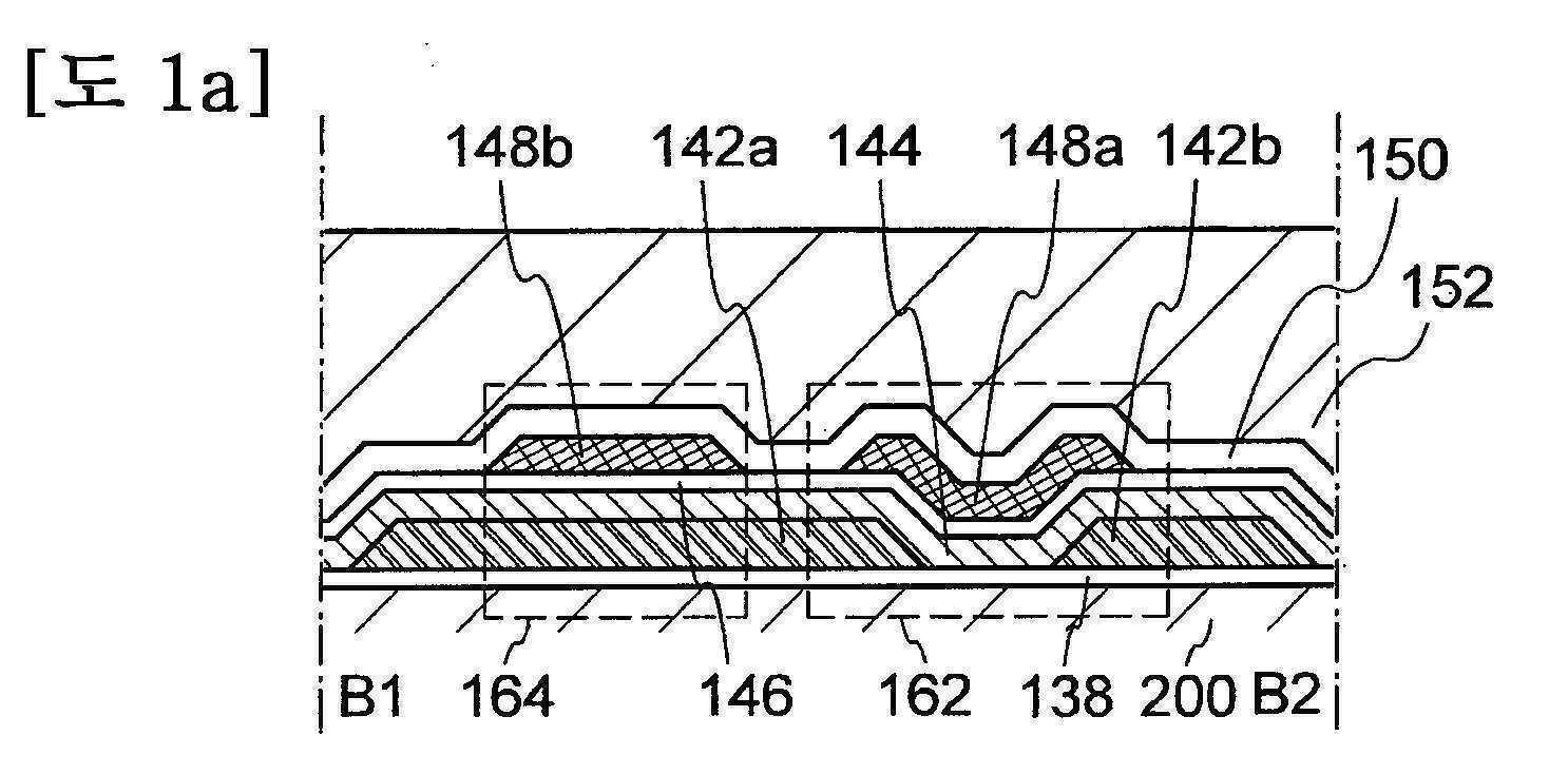
도 1a 내지 도 1d는 각각 반도체 장치의 구성의 일례를 도시한다. 도 1a 내지 도 1d는 각각 반도체 장치의 단면도를 도시한다. 도 1a 내지 도 1d에 도시된 반도체 장치는 각각 산화물 반도체를 사용한 트랜지스터(162) 및 용량 소자(164)를 포함한다.1A to 1D each show an example of the configuration of a semiconductor device. 1A to 1D each show a cross-sectional view of a semiconductor device. The semiconductor device shown in FIGS. 1A to 1D includes a
또한, 상기 트랜지스터는 모두 n-채널형 트랜지스터인 것으로서 설명하지만, p-채널형 트랜지스터를 사용할 수 있는 것은 말할 필요도 없다. 또한, 개시하는 발명의 기술적인 본질은 데이터를 저장하기 위해서 산화물 반도체를 트랜지스터(162)에 사용하는 점에 있기 때문에, 반도체 장치의 구체적인 구성을 여기에서 나타내는 것에 한정할 필요는 없다.In addition, although all of the above transistors are described as being n-channel type transistors, it goes without saying that p-channel type transistors can be used. In addition, since the technical essence of the disclosed invention lies in the use of an oxide semiconductor for the
도 1a의 트랜지스터(162)는 기판(200) 위에 절연층(138)을 개재하여 소스 또는 드레인 전극(142a) 및 소스 또는 드레인 전극(142b), 상기 소스 또는 드레인 전극(142a) 및 상기 소스 또는 드레인 전극(142b)에 전기적으로 접속되어 있는 산화물 반도체층(144), 상기 소스 또는 드레인 전극(142a), 상기 소스 또는 드레인 전극(142b), 및 상기 산화물 반도체층(144)을 덮는 게이트 절연층(146), 및 상기 게이트 절연층(146) 위에 상기 산화물 반도체층(144)과 중첩하도록 제공된 게이트 전극(148a)을 가진다. The
여기에서, 상기 산화물 반도체층(144)은 수소와 같은 불순물을 충분하게 제거함으로써 또는 충분한 산소를 공급함으로써 고순도화된 산화물 반도체층인 것이 바람직하다. 구체적으로는, 상기 산화물 반도체층(144)의 수소 농도는 5×10¹⁹atoms/㎤ 이하, 바람직하게는 5×10¹⁸atoms/㎤ 이하, 보다 바람직하게는 5×10¹⁷atoms/㎤ 이하로 한다. 상기 산화물 반도체층(144)의 수소 농도는 2차 이온질량 분석법(SIMS: Secondary Ion Mass Spectrometry)으로 측정된다는 것을 주의한다. 수소의 농도를 충분하게 저감함으로써 고순도화되고, 충분한 산소의 공급에 의해 산소 결핍에 기인하는 에너지 갭의 결함 준위가 저감된 상기 산화물 반도체층(144)에서는, 캐리어 농도가 1×10¹²/㎤ 미만, 바람직하게는 1×10¹¹/㎤ 미만, 보다 바람직하게는 1.45×10¹⁰/㎤ 미만이다. 예를 들면, 실온에서의 오프 전류 밀도(오프 전류를 트랜지스터의 채널 폭으로 나눈 값)는 10zA/㎛ 내지 100zA/㎛(1zA(젭토암페어)는 1×10-21A) 정도가 된다. 이렇게, i형(진성) 산화물 반도체 또는 실질적으로 i형 산화물 반도체로 된 산화물 반도체를 사용함으로써 지극히 우수한 오프 전류 특성의 트랜지스터(162)를 수득할 수 있다. Here, the
도 1a의 상기 트랜지스터(162)는 상기 산화물 반도체층(144)이 섬 형상으로 가공되지 않기 때문에, 패터닝을 위한 에칭에 의한 상기 산화물 반도체층(144)의 오염을 방지할 수 있다는 것을 주의한다. Note that in the
상기 용량 소자(164)는 상기 소스 또는 드레인 전극(142a), 상기 산화물 반도체층(144), 상기 게이트 절연층(146) 및 상기 전극(148b)을 포함한다. 즉, 상기 소스 또는 드레인 전극(142a)은 상기 용량 소자(164)의 한 전극으로서 기능하고, 상기 전극(148b)은 상기 용량 소자(164)의 다른 전극으로서 기능하게 된다. The
도 1a에 도시된 상기 용량 소자(164)에서 상기 산화물 반도체층(144)과 상기 게이트 절연층(146)을 적층함으로써, 상기 소스 또는 드레인 전극(142a)과 상기 전극(148b) 사이의 절연성을 충분하게 확보할 수 있다는 것을 주의한다.By laminating the
상기 트랜지스터(162) 및 상기 용량 소자(164)에 있어서, 상기 소스 또는 드레인 전극(142a), 상기 소스 또는 드레인 전극(142b), 및 절연층(143)의 단부는 테이퍼 형상인 것이 바람직하다. 여기에서, 테이퍼 각은 예를 들면, 30° 이상 60° 이하로 한다는 것을 주의한다. "테이퍼 각"은 테이퍼 형상을 가지는 층(예를 들면, 상기 소스 또는 드레인 전극(142a))을 그 단면(기판의 표면과 직교하는 면)에 수직한 방향에서 관찰했을 때, 상기 층의 측면과 저면에 의해 형성된 경사각을 나타낸다. 상기 소스 또는 드레인 전극(142a) 및 상기 소스 또는 드레인 전극(142b)의 단부를 테이퍼 형상으로 함으로써, 상기 산화물 반도체층(144)의 피복성이 향상되고 절단을 방지할 수 있다. In the
또한, 상기 트랜지스터(162) 및 상기 용량 소자(164) 위에는 층간 절연층(150)이 설치되어 있고, 상기 층간 절연층(150) 위에 층간 절연층(152)이 제공된다. In addition, an
도 1b에 도시된 트랜지스터 및 용량 소자는 도 1a에 도시된 트랜지스터 및 용량 소자의 변형 예이다. The transistor and capacitor shown in FIG. 1B are modified examples of the transistor and capacitor shown in FIG. 1A.
도 1b에 도시된 구성과 도 1a에 도시된 구성과의 차이는 도 1b는 산화물 반도체층이 섬 형상을 갖도록 형성된 점에 있다. 즉, 도 1a에 도시된 구성에서는, 산화물 반도체층(144)이 절연층(138), 소스 또는 드레인 전극(142a) 및 소스 또는 드레인 전극(142b)의 전체를 덮는 반면, 도 1b에 도시된 구성에서는, 섬 형상의 산화물 반도체층(144)이 절연층(138), 상기 소스 또는 드레인 전극(142a) 및 상기 소스 또는 드레인 전극(142b)의 일부를 덮는다. 여기에서, 섬 형상의 산화물 반도체층(144)의 단부는 테이퍼 형상인 것이 바람직하다. 테이퍼 각은 예를 들면, 30° 이상 60° 이하로 하는 것이 바람직하다. The difference between the configuration shown in FIG. 1B and the configuration shown in FIG. 1A is that the oxide semiconductor layer in FIG. 1B is formed to have an island shape. That is, in the configuration shown in FIG. 1A , the
또한, 용량 소자(164)에 있어서, 산화물 반도체층(144)과 게이트 절연층(146)을 적층시킴으로써, 상기 소스 또는 드레인 전극(142a)과 상기 전극(148b) 사이의 절연성을 충분하게 확보할 수 있다. In addition, in the
도 1c에 도시된 트랜지스터 및 용량 소자는 도 1a에 도시된 트랜지스터 및 용량 소자의 다른 변형 예이다. The transistor and capacitor shown in FIG. 1C are another modification of the transistor and capacitor shown in FIG. 1A.
도 1c에 도시된 구성과 도 1a에 나타내는 구성과의 차이는, 도 1c는 절연층(143)이 소스 또는 드레인 전극(142a) 및 소스 또는 드레인 전극(142b) 위에 형성되어 있다는 점이다. 또한, 산화물 반도체층(144)이 절연층(143), 소스 또는 드레인 전극(142a) 및 소스 또는 드레인 전극(142b)을 덮도록 형성되어 있다는 점이다. 또한, 도 1c에 도시된 구성에서, 산화물 반도체층(144)은 절연층(143)에 형성된 개구를 통해 소스 또는 드레인 전극(142a)에 접해서 제공된다. The difference between the configuration shown in FIG. 1C and the configuration shown in FIG. 1A is that, in FIG. 1C , the insulating
절연층(143)이 제공될 때, 게이트 전극과 소스 전극 및 게이트 전극과 드레인 전극의 사이에 형성되는 용량이 저감되어, 트랜지스터의 고속 동작을 실현할 수 있다. When the insulating
도 1d에 도시된 트랜지스터 및 용량 소자는 도 1b 및 도 1c에 도시된 트랜지스터 및 용량 소자와 일부 다른 구성이다. The transistor and capacitor shown in FIG. 1D have some different configurations from the transistor and capacitor shown in FIGS. 1B and 1C.
도 1d에 도시된 구성과 도 1b에 도시된 구성의 차이는, 도 1d는 소스 또는 드레인 전극(142a) 및 소스 또는 드레인 전극(142b) 위에 절연층(143)이 형성되어 있다는 점이다. 또한, 산화물 반도체층(144)이 절연층(143), 소스 또는 드레인 전극(142a) 및 소스 또는 드레인 전극(142b)을 덮도록 형성되어 있다는 점이다. 또한, 도 1d에 도시된 구성과 도 1c에 도시된 구성의 차이는, 도 1d는 섬 형상을 갖도록 형성된 산화물 반도체층(144)을 포함한다는 점이다. 상기 구성에 의해, 도 1b의 구성으로 획득되는 효과와 도 1c의 구성으로 획득되는 효과를 모두 수득할 수 있다. The difference between the configuration shown in FIG. 1D and the configuration shown in FIG. 1B is that the insulating
<반도체 장치의 회로 구성 및 동작><Circuit configuration and operation of semiconductor device>
다음에, 상기 반도체 장치의 회로 구성의 예 및 그 동작에 관하여 설명한다. 도 2a1, 도 2a2, 및 도 2b는 도 1a, 도 1b, 도 1c 또는 도 1d에 도시된 반도체 장치를 사용한 회로 구성의 예이다. Next, an example of the circuit configuration of the semiconductor device and its operation will be described. 2A1, 2A2, and 2B are examples of circuit configurations using the semiconductor device shown in FIG. 1A, 1B, 1C or 1D.
도 2a1에 도시된 반도체 장치에 있어서, 제 1 배선(소스선이라고도 부르는)과 트랜지스터(160)의 소스 전극은 서로 전기적으로 접속되고, 제 2 배선(비트선이라고도 부르는)과 트랜지스터(160)의 드레인 전극은 서로 전기적으로 접속되어 있다. 또한, 제 3 배선(제 1 신호선이라고도 부르는)과 트랜지스터(162)의 소스 전극 및 드레인 전극 중 하나는 서로 전기적으로 접속되고, 제 4 배선(제 2 신호선이라고도 부르는)과 트랜지스터(162)의 게이트 전극은 서로 전기적으로 접속되어 있다. 트랜지스터(160)의 게이트 전극, 트랜지스터(162)의 소스 전극 및 드레인 전극 중 다른 하나 및 용량 소자(164)의 한 전극은 서로 전기적으로 접속된다. 또한, 제 5 배선(워드선이라고도 부르는)과 용량 소자(164)의 다른 전극은 서로 전기적으로 접속되어 있다. In the semiconductor device shown in FIG. 2A1 , the first wiring (also called a source line) and the source electrode of the
여기에서, 트랜지스터(160) 및 트랜지스터(162)로서 상기의 산화물 반도체를 사용한 트랜지스터가 사용된다. 상기의 산화물 반도체를 사용한 트랜지스터는 오프 전류가 지극히 낮은 특징을 가지고 있다. 이 때문에, 트랜지스터(162)가 턴오프될 때, 트랜지스터(160)의 게이트 전극의 전위를 지극히 장시간에 걸쳐 유지하는 것이 가능하다. 용량 소자(164)를 제공함으로써 트랜지스터(160)의 게이트 전극에 주어진 전하의 유지 및 저장된 데이터의 판독이 용이해진다. 산화물 반도체를 사용한 트랜지스터(162)는 10nm 이상 1000nm 이하의 채널 길이(L)를 갖기 때문에, 소비 전력이 작아지고, 매우 고속으로 동작할 수 있다는 것을 주의한다.Here, transistors using the above oxide semiconductor are used as the
도 2a1에 도시된 반도체 장치는 트랜지스터(160)의 게이트 전극의 전위가 유지가능하다는 특징을 사용함으로써 다음과 같이, 데이터의 기록, 저장, 판독이 가능하다. The semiconductor device shown in FIG. 2A1 uses the feature that the potential of the gate electrode of the
먼저, 데이터의 기록 및 저장에 관하여 설명한다. 우선, 제 4 배선의 전위를 트랜지스터(162)가 턴온 상태가 되는 전위로 설정하여, 트랜지스터(162)를 턴온한다. 이것에 의해, 제 3 배선의 전위가 트랜지스터(160)의 게이트 전극 및 용량 소자(164)에 공급된다. 즉, 트랜지스터(160)의 게이트 전극에 소정의 전하가 주어진다(기록). 여기에서는, 전위 레벨의 공급을 위한 전하 또는 상이한 전위 레벨을 공급하기 위한 전하(이하 Low 레벨 전하 및 High 레벨 전하라고 한다)가 주어진다. 그 후에 제 4 배선의 전위를 트랜지스터(162)가 턴오프하는 전위로 설정하여, 트랜지스터(162)가 턴오프된다. 따라서, 트랜지스터(160)의 게이트 전극에 주어진 전하가 유지된다(저장). First, recording and storage of data will be described. First, the potential of the fourth wiring is set to a potential at which the
트랜지스터(162)의 오프 전류는 지극히 작기 때문에, 트랜지스터(160)의 게이트 전극의 전하는 장시간에 걸쳐 유지된다. Since the off current of the
다음에, 데이터의 판독에 관하여 설명한다. 제 1 배선에 소정의 전위(정전위)가 공급되는 동안 제 5 배선에 적절한 전위(판독 전위)를 공급함으로써, 트랜지스터(160)의 게이트 전극에 유지된 전하량에 따라, 제 2 배선의 전위가 변한다. 일반적으로, 트랜지스터(160)가 n-채널 트랜지스터라고 하면, 트랜지스터(160)의 게이트 전극에 High 레벨 전하가 주어지는 경우 겉보기 임계 전압(Vth_H)은 트랜지스터(160)의 게이트 전극에 Low 레벨 전하가 주어지는 경우의 겉보기 임계 전압(Vth_L)보다 낮기 때문이다. 여기에서, 겉보기 임계 전압은 트랜지스터(160)를 턴온하기 위해서 필요한 제 5 배선의 전위를 말한다. 따라서, 제 5 배선의 전위를 Vth_H와 Vth_L의 중간의 전위(V0)로 함으로써, 트랜지스터(160)의 게이트 전극에 주어지는 전하를 결정할 수 있다. 예를 들면, 기록에 있어서, High 레벨 전하가 주어지는 경우에는, 제 5 배선의 전위가 V0(>Vth_H)이 되면, 트랜지스터(160)는 턴온된다. 기록에 있어서, Low 레벨 전하가 주어지는 경우에는, 제 5 배선의 전위가 V0(<Vth_L)이 되어도, 트랜지스터(160)는 오프 상태로 유지된다. 이 때문에, 제 2 배선의 전위에 의해 저장된 데이터가 판독될 수 있다. Next, the reading of data will be described. By supplying an appropriate potential (read potential) to the fifth wiring while a predetermined potential (positive potential) is supplied to the first wiring, the potential of the second wiring changes according to the amount of electric charge held in the gate electrode of the
메모리 셀을 어레이 모양으로 배치해서 사용할 경우에는, 원하는 메모리 셀의 데이터만을 판독할 필요가 있다는 것을 주의한다. 따라서, 소정의 메모리 셀의 데이터를 판독하고, 그 이외의 메모리 셀의 데이터를 판독하지 않도록 하기 위해서, 메모리 셀들 간에서 트랜지스터(160)가 병렬로 접속되어 있는 경우, 게이트 전극의 상태와 상관없이 트랜지스터(160)가 턴오프되도록 하는 전위, 즉 데이터가 판독되지 않는 메모리 셀의 제 5 배선에 Vth_H보다 작은 전위가 공급된다. 메모리 셀들 간에서 트랜지스터(160)가 직렬로 접속되어 있을 경우에는, 게이트 전극의 상태와 상관없이 트랜지스터(160)가 턴온되도록 하는 전위, 제 5 배선에 Vth_L보다 큰 전위가 공급된다.Note that when memory cells are arranged in an array and used, it is necessary to read only the data of the desired memory cells. Therefore, when the
다음에, 데이터의 재기록에 관하여 설명한다. 데이터의 재기록은 상기 데이터의 기록 및 저장과 유사하게 실시된다. 즉, 제 4 배선의 전위를 트랜지스터(162)가 턴온되는 전위로 설정하여, 트랜지스터(162)를 턴온한다. 이것에 의해, 제 3 배선의 전위(새로운 데이터에 관계되는 전위)가 트랜지스터(160)의 게이트 전극 및 용량 소자(164)에 공급된다. 그 후에 제 4 배선의 전위를 트랜지스터(162)가 턴오프되는 전위로 설정하여, 트랜지스터(162)를 턴오프한다. 따라서, 트랜지스터(160)의 게이트 전극에 새로운 데이터에 관계되는 전하가 주어진다. Next, data rewriting will be described. Rewriting of data is performed similarly to writing and storing of the above data. That is, the potential of the fourth wiring is set to the potential at which the
개시하는 발명에 따른 반도체 장치에서, 상기와 같이 데이터의 다른 기록에 의해 직접적으로 데이터가 재기록될 수 있다. 이 때문에 플래시 메모리 등에 필요한 소거 동작이 필요하지 않아서, 소거 동작에 기인하는 동작 속도의 저하를 억제할 수 있다. 즉, 반도체 장치의 고속 동작이 실현된다. In the semiconductor device according to the disclosed invention, data can be directly rewritten by another recording of data as described above. For this reason, an erase operation necessary for a flash memory or the like is not required, and a decrease in the operation speed due to the erase operation can be suppressed. That is, high-speed operation of the semiconductor device is realized.
트랜지스터(162)의 소스 전극 또는 드레인 전극은 트랜지스터(160)의 게이트 전극에 전기적으로 접속되어, 비휘발성 메모리 소자로서 사용할 수 있는 플로팅 게이트 트랜지스터의 플로팅 게이트와 유사한 효과를 갖는다. 이 때문에, 도면 중, 트랜지스터(162)의 소스 전극 또는 드레인 전극과 트랜지스터(160)의 게이트 전극이 서로 전기적으로 접속되는 부위를 플로팅 게이트부(FG)라고 부를 경우가 있다. 트랜지스터(162)가 오프일 때, 상기 플로팅 게이트부(FG)는 절연체에 임베딩되었다고 볼 수 있고, 따라서 플로팅 게이트부(FG)에는 전하가 유지된다. 산화물 반도체를 사용한 트랜지스터(162)의 오프 전류량은 실리콘 등을 사용하여 형성되는 트랜지스터의 오프 전류량의 10 만분의 1 이하이기 때문에, 트랜지스터(162)의 리크 전류에 의해 플로팅 게이트부(FG)에 축적되는 전하의 소실은 무시할 수 있다. 즉, 산화물 반도체를 사용한 트랜지스터(162)에 의해, 비휘발성의 메모리 장치를 실현하는 것이 가능하다. A source electrode or a drain electrode of the
예를 들면, 트랜지스터(162)의 실온에서의 오프 전류 밀도가 10zA(1zA(젭토암페어)는 1×10-21A)정도이며, 용량 소자(164)의 용량값이 1pF정도일 경우에는, 적어도 106초 이상 데이터 저장이 가능하다. 상기 저장 시간이 트랜지스터 특성이나 용량값에 따른다는 것은 말할 필요도 없다. For example, when the off-state current density of the
또한, 이 경우, 종래의 플로팅 게이트형 트랜지스터에 있어서 지적된 게이트 절연막(터널 절연막)의 열화라고 하는 문제가 존재하지 않는다. 즉, 종래 문제라고 하는, 전자의 플로팅 게이트로의 주입으로 인한 게이트 절연막의 열화가 회피될 수 있다. 이것은, 이론적으로 기록 회수의 제한이 없다는 것을 의미하는 것이다. 또한, 종래의 플로팅 게이트형 트랜지스터에 있어서 기록이나 소거 때에 필요했던 고전압도 필요하지 않다. Further, in this case, the problem of deterioration of the gate insulating film (tunnel insulating film) pointed out in the conventional floating gate type transistor does not exist. That is, deterioration of the gate insulating film due to the injection of electrons into the floating gate, which is a conventional problem, can be avoided. This means that theoretically there is no limit to the number of recordings. Also, the high voltage required for writing or erasing in the conventional floating gate transistor is not required.
도 2a1에 도시된 반도체 장치의 회로 구성은 포함된 트랜지스터 등의 요소가 상기 반도체 장치에 저항 및 용량 소자를 포함하는 도 2a2에 도시된 회로 구성과 교체 가능하다. 즉, 도 2a2에서는, 트랜지스터(160) 및 용량 소자(164)는 각각 저항 및 용량 소자를 포함하는 것으로 고려된다. R1 및 C1은 각각 용량 소자(164)의 저항값 및 용량값이다. 저항값(R1)은 용량 소자(164)에 포함된 절연층에 따른 저항값에 상당한다. R2 및 C2는 각각 트랜지스터(160)의 저항값 및 용량값이다. 저항값(R2)은 트랜지스터(160)가 온일 때의 트랜지스터(160)에 포함된 게이트 절연층에 따른 저항값에 상당한다. 용량값(C2)은 소위 게이트 용량(게이트 전극과 소스 전극 사이 및 게이트 전극과 드레인 전극 사이에 형성되는 용량)값에 상당한다. 저항값(R2)은 트랜지스터(160)의 게이트 전극과 채널 형성 영역 사이의 저항값만을 나타내고, 이 점을 명확히 하기 위해서, 접속의 일부를 점선으로 나타내고 있다는 것을 주의한다. The circuit configuration of the semiconductor device shown in FIG. 2A1 is interchangeable with the circuit configuration shown in FIG. 2A2 in which elements such as transistors included include resistors and capacitors in the semiconductor device. That is, in FIG. 2A2 , the
트랜지스터(162)가 오프 상태에 있을 경우의 소스 전극과 드레인 전극의 사이의 저항값(실효저항이라고도 부르는)을 ROS라고 하면, R1 및 R2가 R1≥ROS(R1은 ROS 이상), R2≥ROS(R2는 ROS 이상)를 충족시킬 경우에는, 전하의 유지 시간(데이터 저장 기간이라고 할 수도 있는)은 주로 트랜지스터(162)의 오프 전류에 의해 결정되게 된다. If the resistance value (also called effective resistance) between the source electrode and the drain electrode when the
반대로, 상기 관계를 충족시키지 않을 경우에는, 트랜지스터(162)의 오프 전류가 충분히 작더라도, 유지 시간을 충분하게 확보하는 것이 곤란해진다. 트랜지스터(162) 이외의 부분에서 생성된 리크 전류량이 크기 때문이다. 따라서, 본 실시형태에 있어서 개시하는 반도체 장치는 상기의 관계를 만족시키는 것이 바람직하다고 할 수 있다. Conversely, if the above relationship is not satisfied, it becomes difficult to sufficiently ensure the holding time even if the off current of the
C1과 C2는 C1≥C2(C1은 C2 이상)의 관계를 만족하는 것이 바람직하다. C1이 크면, 제 5 배선에 의해 플로팅 게이트부(FG)의 전위를 제어할 때(예를 들면, 판독 시), 제 5 배선의 전위의 변동을 낮게 할 수 있다. It is preferable that C1 and C2 satisfy the relationship of C1≥C2 (C1 is C2 or more). When C1 is large, when the potential of the floating gate portion FG is controlled by the fifth wiring (eg, during reading), the fluctuation of the potential of the fifth wiring can be reduced.
상기의 관계가 충족될 때, 보다 바람직한 반도체 장치를 실현하는 것이 가능하다. R1 및 R2는 트랜지스터(160) 및 트랜지스터(162)의 게이트 절연층에 의해 제어된다는 것을 주의한다. C1 및 C2도 유사하게 제어된다. 따라서, 게이트 절연층의 재료, 두께 등을 적절히 설정하고, 상기의 관계를 만족하도록 하는 것이 바람직하다. When the above relationship is satisfied, it is possible to realize a more preferable semiconductor device. Note that R1 and R2 are controlled by the gate insulating layer of
도 2b에 도시된 반도체 장치는 도 2a1에 도시된 트랜지스터(160)를 설치하지 않는 구성의 반도체 장치이다. 도 2b에 도시된 반도체 장치에 있어서, 제 1 배선(제 1 신호선이라고도 부르는)과 트랜지스터(162)의 소스 전극 및 드레인 전극 중 하나는 서로 전기적으로 접속된다. 제 2 배선(제 2 신호선이라고도 부르는)과 트랜지스터(162)의 게이트 전극은 서로 전기적으로 접속되어 있다. 그리고, 트랜지스터(162)의 소스 전극 및 드레인 전극의 다른 하나와 용량 소자(164)의 한 전극은 서로 전기적으로 접속된다. 제 3 배선(용량선이라고도 부르는)과 용량 소자(164)의 다른 전극은 서로 전기적으로 접속되어 있다. The semiconductor device shown in FIG. 2B is a semiconductor device having a configuration in which the
여기에서, 트랜지스터(162)로서 상기의 산화물 반도체를 사용한 트랜지스터가 적용된다. 상기의 산화물 반도체를 사용한 트랜지스터는 오프 전류가 지극히 작다고 하는 특징을 가지고 있다. 이 때문에, 트랜지스터(162)가 턴오프될 때, 용량 소자(164)에 공급된 전위를 지극히 장시간 동안 유지하는 것이 가능하다. 산화물 반도체를 사용한 트랜지스터(162)는 10nm 이상 1000nm 이하의 채널 길이(L)를 갖기 때문에, 소비 전력이 작고, 동작 속도가 지극히 크다.Here, a transistor using the above oxide semiconductor is applied as the
도 2b에 도시된 반도체 장치는 용량 소자(164)에 공급된 전위가 유지된다는 특징을 이용하여 다음과 같이, 데이터의 기록, 저장, 판독이 가능하다. In the semiconductor device shown in FIG. 2B, data can be written, stored, and read as follows by using the characteristic that the potential supplied to the
처음에, 데이터의 기록 및 저장에 관하여 설명한다. 간략화를 위하여, 제 3 배선의 전위는 고정된다. 우선, 제 2 배선의 전위를 트랜지스터(162)가 턴온되는 전위로 설정하여, 트랜지스터(162)가 턴온된다. 이러한 방식으로, 제 1 배선의 전위가 용량 소자(164)의 한 전극에 공급된다. 즉, 용량 소자(164)에는 소정의 전하가 주어진다(기록). 그 후에 제 2 배선의 전위를 트랜지스터(162)가 턴오프되는 전위로 설정하여, 트랜지스터(162)가 턴오프된다. 따라서, 용량 소자(164)에 주어진 전하가 유지된다(저장). 트랜지스터(162)는 전술한 바와 같이, 지극히 오프 전류가 작으므로, 장시간 동안 전하를 유지할 수 있다. First, recording and storage of data will be described. For simplicity, the potential of the third wiring is fixed. First, the potential of the second wiring is set to the potential at which the
다음에, 데이터의 판독에 관하여 설명한다. 제 1 배선에 소정의 전위(정전위)가 공급되는 동안, 제 2 배선의 전위를 트랜지스터(162)를 턴온하는 전위로 설정함으로써, 용량 소자(164)에 유지되어 있는 전하량에 따라 제 1 배선의 전위가 변한다. 이 때문에, 제 1 배선의 전위에 의해 저장된 데이터를 판독할 수 있다. Next, the reading of data will be described. While a predetermined potential (positive potential) is supplied to the first wiring, by setting the potential of the second wiring to a potential that turns on the
데이터가 판독되는 경우, 용량 소자(164)의 전하는 손실되기 때문에, 다른 기록을 행하는 점을 주의한다. Note that when data is read out, since the charge of the
다음에, 데이터의 재기록에 관하여 설명한다. 데이터의 재기록은 상기 데이터의 기록 및 저장과 마찬가지로 실시된다. 즉, 제 2 배선의 전위를 트랜지스터(162)가 턴온되는 전위로 설정하여, 트랜지스터(162)가 턴온된다. 이것에 의해, 제 1 배선의 전위(새로운 데이터에 관계되는 전위)가 용량 소자(164)의 한 전극에 공급된다. 그 후에 제 2 배선의 전위를 트랜지스터(162)가 턴오프되는 전위로 설정하여, 트랜지스터(162)가 턴오프된다. 따라서, 용량 소자(164)에 새로운 데이터에 관계되는 전하가 주어진다. Next, data rewriting will be described. Rewriting of data is performed similarly to writing and storing of the above data. That is, by setting the potential of the second wiring to the potential at which the
개시하는 발명의 일 실시형태에 따른 반도체 장치는 상기와 같이 데이터의 다른 기록에 의해 직접적으로 데이터를 재기록하는 것이 가능하다. 이 때문에, 반도체 장치의 고속 동작이 실현된다. In the semiconductor device according to an embodiment of the disclosed invention, data can be directly rewritten by another recording of data as described above. For this reason, high-speed operation of the semiconductor device is realized.
상기 설명은 전자가 다수 캐리어인 n-채널 트랜지스터가 사용된다는 것을 주의한다. 그러나, n-채널 트랜지스터 대신에, 정공이 다수 캐리어인 p-채널 트랜지스터를 사용할 수 있는 것은 말할 필요도 없다. Note that the above description uses an n-channel transistor in which electrons are majority carriers. However, it goes without saying that instead of the n-channel transistor, a p-channel transistor in which holes are majority carriers can be used.
(실시형태 2)(Embodiment 2)
본 실시형태에서는 산화물 반도체를 사용한 반도체 장치의 제작 방법, 구체적으로는, 트랜지스터(162)의 제작 방법에 대해서, 도 3a 내지 도 3e를 참조하여 설명한다. In the present embodiment, a method of manufacturing a semiconductor device using an oxide semiconductor, specifically, a method of manufacturing the
우선, 기판(200) 위에 절연층(138)을 형성한다. 그 후에 절연층(138) 위에 도전층을 형성하고 선택적으로 에칭하여, 소스 또는 드레인 전극(142a) 및 소스 또는 드레인 전극(142b)이 형성된다(도 3a 참조). First, an insulating
상기 기판(200)으로서, 예를 들어, 유리 기판이 사용될 수 있다. 대안적으로, 상기 기판(200)으로서, 유리 기판뿐만 아니라, 세라믹 기판, 석영 기판, 또는 사파이어 기판과 같은 절연체를 사용하여 형성된 절연 기판, 실리콘과 같은 반도체 재료를 사용하여 형성된 반도체 기판, 금속 또는 스테인레스 스틸과 같은 도전체를 사용하여 형성된 도전성 기판, 표면이 절연 재료로 덮인 임의의 이들 기판, 등을 사용할 수 있다. 또한, 플라스틱과 같은 가요성 기판은 일반적으로 낮은 내열성을 갖는 경향이 있지만, 나중의 제조 공정의 처리 온도를 견딜 수 있는 기판이면 상기 기판(200)으로서 사용될 수 있다.As the
절연층(138)은 하지로서 기능하는 것이며, PVD법이나 CVD법 등을 사용하여 형성할 수 있다. 절연층(138)은 산화 실리콘, 산화질화 실리콘, 질화 실리콘, 산화 하프늄, 산화 알루미늄, 산화 탄탈 등의 무기 절연 재료를 포함하는 재료를 사용하여 형성할 수 있다. 절연층(138)은 가능한 한 수소나 수분을 포함하지 않도록 형성하는 것이 바람직하다는 것을 주의한다. 절연층(138)을 설치하지 않는 구성으로 하는 것도 가능하다. The insulating
도전층은 스퍼터링법을 비롯한 PVD법이나, 플라즈마 CVD법 등의 CVD법을 사용하여 형성할 수 있다. 도전층의 재료로서는, 알루미늄, 크롬, 구리, 탄탈, 티타늄, 몰리브덴, 텅스텐으로부터 선택된 원소나, 상기한 임의의 원소를 성분으로 하는 합금 등을 사용할 수 있다. 또한, 망간, 마그네슘, 지르코늄, 베릴륨으로부터 선택된 하나 이상의 재료들이 사용될 수 있다. 대안적으로, 알루미늄에 티타늄, 탄탈, 텅스텐, 몰리브덴, 크롬, 네오디뮴, 스칸듐으로부터 선택된 하나 이상의 원소를 조합시킨 재료를 사용해도 된다. The conductive layer can be formed using a PVD method including a sputtering method or a CVD method such as a plasma CVD method. As the material of the conductive layer, an element selected from aluminum, chromium, copper, tantalum, titanium, molybdenum, and tungsten, an alloy containing any of the above elements as a component, or the like can be used. Also, one or more materials selected from manganese, magnesium, zirconium, and beryllium may be used. Alternatively, a material in which aluminum is combined with one or more elements selected from titanium, tantalum, tungsten, molybdenum, chromium, neodymium, and scandium may be used.
도전층은 단층 구조이어도 양호하고, 2층 이상의 적층 구조로 해도 된다. 예를 들면, 티타늄 막이나 질화 티타늄 막의 단층 구조, 실리콘을 함유하는 알루미늄 막의 단층 구조, 알루미늄 막 위에 티타늄 막이 적층된 2층 구조, 질화 티타늄 막 위에 티타늄 막이 적층된 2층 구조, 티타늄 막과 알루미늄 막과 티타늄 막이 적층된 3층 구조 등을 들 수 있다. 도전층을 티타늄 막이나 질화 티타늄 막의 단층 구조라고 할 경우에는, 테이퍼 형상을 가지는 소스 또는 드레인 전극(142a) 및 소스 또는 드레인 전극(142b)으로의 가공이 용이하다고 하는 장점이 있다는 것을 주의한다. A single layer structure may be sufficient as a conductive layer, and it is good also as a laminated structure of two or more layers. For example, a single-layer structure of a titanium film or a titanium nitride film, a single-layer structure of an aluminum film containing silicon, a two-layer structure in which a titanium film is laminated on an aluminum film, a two-layer structure in which a titanium film is laminated on a titanium nitride film, a titanium film and an aluminum film and a three-layer structure in which a titanium film is laminated. Note that when the conductive layer is a single-layer structure of a titanium film or a titanium nitride film, there is an advantage in that it is easy to process the source or
대안적으로, 도전층은 도전성 금속 산화물을 사용하여 형성될 수 있다. 도전성의 금속 산화물로서는 산화 인듐(In2O3), 산화 주석(SnO2), 산화 아연(ZnO), 산화 인듐-산화 주석 합금(In2O3-SnO2, ITO로 약기할 경우가 있음), 산화 인듐-산화 아연 합금(In2O3-ZnO), 또는 이들 금속 산화물 재료에 실리콘 또는 산화 실리콘을 함유시킨 것을 사용할 수 있다. Alternatively, the conductive layer may be formed using a conductive metal oxide. Examples of the conductive metal oxide include indium oxide (In 2 O 3 ), tin oxide (SnO 2 ), zinc oxide (ZnO), and indium oxide-tin oxide alloy (In 2 O 3 -SnO 2 , sometimes abbreviated as ITO). , an indium oxide-zinc oxide alloy (In 2 O 3 -ZnO), or a metal oxide material containing silicon or silicon oxide can be used.
도전층은 소스 또는 드레인 전극(142a) 및 소스 또는 드레인 전극(142b)의 단부가 테이퍼되도록 에칭되는 것이 바람직하다. 여기에서, 테이퍼 각은, 예를 들면, 30° 이상 60° 이하인 것이 바람직하다. "테이퍼 각"은 테이퍼 형상을 가지는 층(예를 들면, 소스 또는 드레인 전극(142a))을 그 단면(기판의 표면과 직교하는 면)에 수직한 방향에서 관찰했을 때에, 상기 층의 측면과 저면이 이루는 경사각을 나타낸다는 것을 주의한다. 소스 또는 드레인 전극(142a) 및 소스 또는 드레인 전극(142b)의 단부를 테이퍼되도록 에칭함으로써, 나중에 형성되는 게이트 절연층(146)의 피복성이 향상되고, 절단을 방지할 수 있다. The conductive layer is preferably etched so that ends of the source or
트랜지스터의 채널 길이(L)는 소스 또는 드레인 전극(142a)의 하단부와 소스 또는 드레인 전극(142b)의 하단부 사이의 거리에 의해 결정된다. 트랜지스터의 채널 길이(L)가 25nm 미만인 경우, 수nm 내지 수십nm로 파장이 짧은 초자외선(Extreme Ultraviolet)을 사용해서 마스크를 형성하기 위해 노광을 행하는 것이 바람직하다는 것을 주의한다. 초자외선에 의한 노광은 해상도가 높고 초점 심도도 크다. 따라서, 나중에 형성되는 트랜지스터의 채널 길이(L)를 10nm 이상 1000nm(1㎛) 이하로 하는 것도 가능해서, 회로는 더 고속으로 동작할 수 있다. 또한, 미세화에 의해, 반도체 장치의 소비 전력을 저감하는 것도 가능하다. The channel length L of the transistor is determined by the distance between the lower end of the source or
소스 또는 드레인 전극(142a) 및 소스 또는 드레인 전극(142b) 위에 절연층을 형성할 수 있다는 것을 주의한다. 상기 절연층을 설치함으로써, 나중에 형성되는 게이트 전극과 소스 또는 드레인 전극(142a) 및 상기 게이트 전극과 소스 또는 드레인 전극(142b) 사이의 기생 용량을 저감하는 것이 가능하다. Note that an insulating layer may be formed over the source or
다음에, 소스 또는 드레인 전극(142a) 및 소스 또는 드레인 전극(142b)을 덮도록 산화물 반도체층(144)을 형성한다(도 3b 참조). Next, an
산화물 반도체층(144)은 4원계 금속 산화물인 In-Sn-Ga-Zn-O계 산화물 반도체, 3원계 금속 산화물인 In-Ga-Zn-O계 산화물 반도체, In-Sn-Zn-O계 산화물 반도체, In-Al-Zn-O계 산화물 반도체, Sn-Ga-Zn-O계 산화물 반도체, Al-Ga-Zn-O계 산화물 반도체, Sn-Al-Zn-O계 산화물 반도체, 2원계 금속 산화물인 In-Zn-O계 산화물 반도체, Sn-Zn-O계 산화물 반도체, Al-Zn-O계 산화물 반도체, Zn-Mg-O계 산화물 반도체, Sn-Mg-O계 산화물 반도체, In-Mg-O계 산화물 반도체, 1원계 금속 산화물인 In-O계 산화물 반도체, Sn-O계 산화물 반도체, Zn-O계 산화물 반도체 등의 산화물 반도체를 사용하여 형성할 수 있다.The
특히, In-Ga-Zn-O계 산화물 반도체 재료는 무전계일 때 충분히 높은 저항을 가져 오프 전류를 충분하게 저감하는 것이 가능하다. 또한, 전계 효과 이동도도 높기 때문에, In-Ga-Zn-O계 산화물 반도체 재료는 반도체 장치에 사용하는 반도체 재료로서는 바람직하다. In particular, the In-Ga-Zn-O-based oxide semiconductor material has a sufficiently high resistance in the absence of an electric field, so that it is possible to sufficiently reduce the off-state current. Moreover, since the field effect mobility is also high, an In-Ga-Zn-O type|system|group oxide semiconductor material is preferable as a semiconductor material used for a semiconductor device.
In-Ga-Zn-O계 산화물 반도체 재료의 대표 예로서는, InGaO3(ZnO)m(m>0, m:자연수로 제한되지 않음)으로 표기되는 것이 있다. 또한, Ga 대신에 M을 사용하여, InMO3(ZnO)m(m>0, m:자연수로 제한되지 않음)과 같이 표기되는 산화물 반도체 재료가 있다. 여기에서, M은 갈륨(Ga), 알루미늄(Al), 철(Fe), 니켈(Ni), 망간(Mn), 코발트(Co) 등으로부터 선택된 하나 이상의 금속 원소를 나타낸다. 예를 들면, M으로서는, Ga, Ga 및 Al, Ga 및 Fe, Ga 및 Ni, Ga 및 Mn, Ga 및 Co 등을 적용할 수 있다. 상기의 조성은 산화물 반도체 재료가 단지 예일 뿐인 결정 구조로부터 도출되는 것이라는 것을 주의한다. Representative examples of the In-Ga-Zn-O-based oxide semiconductor material include those represented by InGaO 3 (ZnO) m (m>0, m: not limited to a natural number). Also, there is an oxide semiconductor material denoted as InMO 3 (ZnO) m (m>0, m: not limited to a natural number) using M instead of Ga. Here, M represents one or more metal elements selected from gallium (Ga), aluminum (Al), iron (Fe), nickel (Ni), manganese (Mn), cobalt (Co), and the like. For example, as M, Ga, Ga and Al, Ga and Fe, Ga and Ni, Ga and Mn, Ga and Co, etc. are applicable. Note that the above composition is derived from the crystal structure of the oxide semiconductor material, which is merely an example.
산화물 반도체층(144)을 스퍼터링법으로 제작하기 위한 타겟으로서는, In:Ga:Zn=1:x:y(x는 0 이상, y는 0.5 이상 5 이하)의 조성식으로 표현된 것을 사용하는 것이 바람직하다. 예를 들면, In2O3:Ga2O3:ZnO=1:1:2[mol수비]의 조성비를 가지는 타겟 등을 사용할 수 있다. 대안적으로, In2O3:Ga2O3:ZnO=1:1:1[mol수비]의 조성비를 가지는 타겟이나, In2O3:Ga2O3:ZnO=1:1:4[mol수비]의 조성비를 가지는 타겟이나, In2O3:ZnO=1:2[mol수비]의 조성비를 가지는 타겟을 사용할 수도 있다. As a target for producing the
본 실시형태에서는, 비정질 구조의 산화물 반도체층(144)이 In-Ga-Zn-O계 금속 산화물 타겟을 사용하여 스퍼터링법에 의해 형성된다. In this embodiment, the
금속 산화물 타겟 중의 금속 산화물의 상대 밀도는 80% 이상, 바람직하게는 95% 이상, 더 바람직하게는 99.9% 이상이다. 상대 밀도가 높은 금속 산화물 타겟을 사용함으로써, 조밀한 구조의 산화물 반도체층(144)을 형성할 수 있다. The relative density of metal oxides in the metal oxide target is at least 80%, preferably at least 95%, more preferably at least 99.9%. By using a metal oxide target having a high relative density, the
산화물 반도체층(144)의 형성 분위기는 희가스(대표적으로는 아르곤) 분위기, 산소 분위기, 또는, 희가스(대표적으로는 아르곤)와 산소의 혼합 분위기로 하는 것이 바람직하다. 구체적으로는, 예를 들면, 수소, 수분, 수산기, 수소화물 등의 불순물이 농도 1ppm 이하(바람직하게는 농도 10ppb 이하)까지 제거된 고순도 가스 분위기를 사용하는 것이 바람직하다. The atmosphere for forming the
산화물 반도체층(144)의 형성시, 예를 들면, 감압 상태로 유지된 처리실에 기판을 유지하고, 기판의 온도가 100℃ 이상 550℃ 미만, 바람직하게는 200℃ 이상 400℃ 이하로 기판이 가열된다. 대안적으로, 산화물 반도체층(144)의 형성 때의 기판의 온도는 실온일 수 있다. 그리고, 처리실 내의 수분을 제거하면서, 수소나 수분 등이 제거된 스퍼터링 가스를 도입하고, 상기 타겟을 사용해서 산화물 반도체층(144)을 형성한다. 기판을 가열하면서 산화물 반도체층(144)을 형성함으로써, 산화물 반도체층(144)에 포함되는 불순물을 저감할 수 있다. 또한, 스퍼터링에 의한 손상을 경감할 수 있다. 처리실 내의 수분을 제거하기 위해서는 흡착형의 진공펌프를 사용하는 것이 바람직하다. 예를 들면, 크라이오 펌프, 이온 펌프, 티타늄 서블리메이션 펌프를 사용할 수 있다. 터보 펌프에 콜드트랩을 부가한 것을 사용해도 된다. 크라이오 펌프 등을 사용해서 배기함으로써, 처리실로부터 수소나 수분 등을 제거함으로써, 산화물 반도체층(144)의 불순물 농도를 저감할 수 있다. When the
산화물 반도체층(144)은, 예를 들면, 기판과 타겟의 사이와의 거리가 170mm, 압력이 0.4Pa, 직류(DC)전력이 0.5kW, 분위기가 산소(산소 유량비 100%) 분위기, 아르곤(아르곤 유량비 100%) 분위기, 또는 산소와 아르곤의 혼합 분위기로 하는 조건 하에서 형성될 수 있다. 펄스 직류(DC)전원을 사용하면, 성막시에 형성되는 분말 상태의 물질(파티클, 먼지라고도 말하는)을 저감할 수 있고, 막 두께 분포도 균일하기 때문에 바람직하다는 것을 주의한다. 산화물 반도체층(144)의 두께는 1nm 이상 50nm 이하, 바람직하게는 1nm 이상 30nm 이하, 보다 바람직하게는 1nm 이상 10nm 이하로 한다. 이러한 두께의 산화물 반도체층(144)을 사용함으로써 미세화로 인한 단채널 효과를 억제하는 것이 가능하다. 사용되는 산화물 반도체 재료나, 반도체 장치의 용도 등에 의해 적절한 두께는 다르기 때문에, 그 두께는, 사용하는 재료나 용도 등에 따라 적절히 설정될 수 있다는 것을 주의한다. The
산화물 반도체층(144)을 스퍼터링법에 의해 형성하기 전에는, 아르곤 가스를 도입해서 플라즈마를 발생시키는 역스퍼터링을 행함으로써 산화물 반도체층(144)이 형성되는 표면(예를 들면 절연층(138)의 표면)의 부착물을 제거하는 것이 바람직하다는 것을 주의한다. 여기에서, 역스퍼터링은 스퍼터링 타겟에 이온을 충돌시키는 통상의 스퍼터링과 반대로, 처리 표면에 이온을 충돌시킴으로써 그 표면을 개질하는 방법이다. 처리 표면에 이온을 충돌시키는 방법의 예는, 아르곤 분위기 하에서 처리 표면에 고주파 전압을 인가하여, 기판 부근에 플라즈마를 생성하는 방법이다. 아르곤 분위기 대신에 질소 분위기, 헬륨 분위기, 산소 분위기 등이 사용될 수 있다는 것을 주의한다. Before the
그 후에 산화물 반도체층(144)에 대하여, 열처리(제 1 열처리)를 행하는 것이 바람직하다. 제 1 열처리에 의해 산화물 반도체층(144)의 과잉 수소(수분 및 수산기를 포함하는)를 제거하여, 산화물 반도체층의 구조가 개선되고, 에너지 갭의 결함 준위를 저감할 수 있다. 제 1 열처리의 온도는 예를 들면, 300℃ 이상 550℃ 미만, 또는 400℃ 이상 500℃ 이하로 한다. After that, the
열처리는 예를 들면, 저항 발열체 등을 사용한 전기로에 피처리물을 도입하고, 질소 분위기 하, 450℃, 1시간 동안 행할 수 있다. 열처리 동안 산화물 반도체층(144)은 대기에 노출되지 않아, 수분이나 수소의 혼입이 방지된다. The heat treatment can be performed, for example, by introducing the object to be treated into an electric furnace using a resistance heating element or the like, and at 450° C. for 1 hour in a nitrogen atmosphere. During the heat treatment, the
열처리 장치는 전기로에 한정되지 않고, 가열된 가스 등의 매체로부터의 열전도 또는 열복사에 의해, 피처리물을 가열하는 장치일 수 있다. 예를 들면, GRTA(Gas Rapid Thermal Anneal) 장치, LRTA(Lamp Rapid Thermal Anneal) 장치 등의 RTA(Rapid Thermal Anneal) 장치를 사용할 수 있다. LRTA 장치는 할로겐 램프, 메탈 할라이드 램프, 크세논 아크 램프, 카본 아크 램프, 고압 나트륨 램프, 고압 수은 램프 등의 램프로부터 방출되는 광(전자파)의 복사에 의해 피처리물을 가열하는 장치이다. GRTA 장치는 고온의 가스를 사용해서 열처리를 행하는 장치이다. 가스로서는 아르곤 등의 희가스, 또는 질소와 같은, 열처리에 의해 피처리물과 반응하지 않는 불활성 가스를 사용할 수 있다. The heat treatment apparatus is not limited to an electric furnace, and may be an apparatus that heats the object to be treated by heat conduction or heat radiation from a medium such as a heated gas. For example, a rapid thermal annealing (RTA) device such as a gas rapid thermal annealing (GRTA) device or a lamp rapid thermal annealing (LRTA) device may be used. The LRTA apparatus is an apparatus that heats an object to be processed by radiation of light (electromagnetic waves) emitted from lamps such as halogen lamps, metal halide lamps, xenon arc lamps, carbon arc lamps, high pressure sodium lamps, and high pressure mercury lamps. The GRTA apparatus is an apparatus for performing heat treatment using a high-temperature gas. As the gas, it is possible to use a noble gas such as argon or an inert gas that does not react with the object to be treated by heat treatment, such as nitrogen.
예를 들면, 제 1 열처리로서, GRTA 처리가 다음과 같이 행해질 수 있다. 가열된 불활성 가스 분위기 중에 피처리물을 투입하고, 몇 분간 가열한 후, 상기 불활성 가스 분위기로부터 피처리물을 꺼낸다. GRTA 처리는 단시간 동안 고온 열처리가 가능하게 한다. 또한, GRTA 처리는 피처리물의 내열온도를 초과하는 온도일 때도 적용이 가능해진다. 처리 동안 불활성 가스를 산소를 포함하는 가스로 바꿀 수 있다는 것을 주의한다. 이는 산소를 포함하는 분위기에서 제 1 열처리를 행함으로써 산소 결핍에 기인하는 에너지 갭의 결함 준위를 저감할 수 있기 때문이다.For example, as the first heat treatment, the GRTA treatment may be performed as follows. The to-be-processed object is thrown in in the heated inert gas atmosphere, and after heating for several minutes, the to-be-processed object is taken out from the said inert gas atmosphere. GRTA treatment enables high-temperature heat treatment for a short period of time. Further, the GRTA treatment can be applied even at a temperature exceeding the heat-resistant temperature of the object to be treated. Note that the inert gas may be replaced with a gas containing oxygen during processing. This is because, by performing the first heat treatment in an atmosphere containing oxygen, the defect level in the energy gap caused by the oxygen deficiency can be reduced.
불활성 가스 분위기로서는, 질소 또는 희가스(헬륨, 네온, 아르곤 등)를 주성분으로 하는 분위기이며, 수분, 수소 등이 포함되지 않는 분위기를 적용하는 것이 바람직하다는 것을 주의한다. 예를 들면, 열처리 장치에 도입하는 질소나, 헬륨, 네온, 아르곤 등의 희가스의 순도를 6N(99.9999%) 이상, 바람직하게는 7N(99.99999%) 이상(즉, 불순물 농도가 1ppm 이하, 바람직하게는 0.1ppm 이하)으로 한다. Note that, as the inert gas atmosphere, it is preferable to apply an atmosphere containing nitrogen or a rare gas (helium, neon, argon, etc.) as a main component and containing no moisture, hydrogen, or the like. For example, the purity of the rare gas such as nitrogen, helium, neon, or argon introduced into the heat treatment apparatus is 6N (99.9999%) or more, preferably 7N (99.99999%) or more (that is, the impurity concentration is 1 ppm or less, preferably is 0.1ppm or less).
어떤 경우든, 제 1 열처리에 의해 불순물을 저감하고, i 형(진성) 또는 실질적으로 i형 산화물 반도체층(144)을 형성함으로써, 지극히 우수한 특성의 트랜지스터를 실현할 수 있다. In any case, by reducing impurities by the first heat treatment and forming the i-type (intrinsic) or substantially i-type
상기의 열처리(제 1 열처리)는 수소나 수분 등을 제거하는 효과가 있기 때문에, 상기 열처리를 탈수화 처리나, 탈수소화 처리 등이라고 부를 수도 있다. 상기 탈수화 처리나, 탈수소화 처리는 예를 들어, 산화물 반도체층의 형성 후나 게이트 절연층의 형성 후, 또는 게이트 전극의 형성 후에 행하는 것도 가능하다. 이러한 탈수화 처리 또는 탈수소화 처리는 1회 또는 복수회 행해도 된다.Since the heat treatment (first heat treatment) has an effect of removing hydrogen, moisture, and the like, the heat treatment may be referred to as a dehydration treatment, a dehydrogenation treatment, or the like. The dehydration treatment and the dehydrogenation treatment may be performed, for example, after the formation of the oxide semiconductor layer, after the formation of the gate insulating layer, or after the formation of the gate electrode. Such dehydration treatment or dehydrogenation treatment may be performed once or plural times.
다음에, 산화물 반도체층(144)에 접하는 게이트 절연층(146)을 형성한다.(도 3c 참조). 게이트 절연층(146)은 CVD법, 스퍼터링법 등을 사용하여 형성할 수 있다. 게이트 절연층(146)은 산화 실리콘, 질화 실리콘, 산화질화 실리콘, 산화 알루미늄, 산화 탄탈, 산화 하프늄, 산화 이트륨, 하프늄 실리케이트(HfSixOy(x>0, y>0)), 질소가 첨가된 하프늄 실리케이트(HfSixOyNz(x>0, y>0, z>0)), 질소가 첨가된 하프늄 알루미네이트(HfAlxOyNz(x>0, y>0, z>0)) 등을 포함하도록 형성하는 것이 바람직하다. 게이트 절연층(146)은 단층 구조 또는 적층 구조로 해도 된다. 그 두께는 특별하게 한정되지 않지만, 반도체 장치를 미세화할 경우에는, 트랜지스터의 동작을 확보하기 위해서 얇게 하는 것이 바람직하다. 예를 들면, 산화 실리콘을 사용할 경우에는, 1nm 이상 100nm 이하, 바람직하게는 10nm 이상 50nm 이하로 설정할 수 있다. Next, a
전술한 바와 같이, 게이트 절연층(146)을 얇게 하면, 터널 효과 등에 기인하는 게이트 리크가 문제가 된다. 게이트 리크의 문제를 해소하기 위해서는, 게이트 절연층(146)에 산화 하프늄, 산화 탄탈, 산화 이트륨, 하프늄 실리케이트(HfSixOy(x>0, y>0)), 질소가 첨가된 하프늄 실리케이트(HfSixOyNz(x>0, y>0, z>0)), 질소가 첨가된 하프늄 알루미네이트(HfAlxOyNz(x>0, y>0, z>0)) 등의 고유전율(high-k) 재료를 사용하면 양호하다. high-k 재료를 게이트 절연층(146)에 사용함으로써 전기적 특성을 확보하면서, 게이트 리크를 방지하기 위해서 막 두께를 크게 하는 것이 가능하게 된다. high-k 재료를 포함하는 막과 산화 실리콘, 질화 실리콘, 산화질화 실리콘, 질화산화 실리콘, 산화 알루미늄 등의 어느 하나를 포함하는 막의 적층 구조가 채용될 수 있다는 것을 주의한다. As described above, when the
게이트 절연층(146)을 형성한 후, 불활성 가스 분위기 하 또는 산소 분위기 하에서 제 2 열처리를 행하는 것이 바람직하다. 열처리의 온도는 200℃ 이상 450℃ 이하, 바람직하게는 250℃ 이상 350℃ 이하이다. 예를 들면, 질소 분위기 하에서 250℃에서, 1시간의 열처리를 행하면 좋다. 제 2 열처리는 트랜지스터의 전기적 특성의 편차를 경감할 수 있다. 또한, 게이트 절연층(146)이 산소를 포함할 경우, 상기 산화물 반도체층(144)의 산소 결손을 보충하도록 산화물 반도체층(144)에 산소가 공급되어 i형(진성 반도체) 또는 실질적으로 i형 산화물 반도체층을 형성할 수도 있다. After the
본 실시형태에서는, 게이트 절연층(146)이 형성된 후에 제 2 열처리를 행하고 있지만, 제 2 열처리의 타이밍은 이것으로 특별하게 한정되지 않는다는 것을 주의한다. 예를 들면, 게이트 전극이 형성된 후에 제 2 열처리를 행해도 된다. 대안적으로, 제 1 열처리에 후속하여 제 2 열처리를 행해도 되고, 제 1 열처리가 제 2 열처리로서 2회 행해질 수 있고, 제 2 열처리가 제 1 열처리로서 2회 행해질 수 있다. Note that although the second heat treatment is performed after the
다음에, 게이트 절연층(146) 위에 산화물 반도체층(144)과 중첩하는 영역에 게이트 전극(148a)을 형성한다(도 3d 참조). 게이트 전극(148a)은 게이트 절연층(146) 위에 도전층을 형성하고 선택적으로 에칭함으로써 형성할 수 있다. 게이트 전극(148a)이 되는 도전층은 스퍼터링법으로 대표되는 PVD법이나, 플라즈마 CVD법과 같은 CVD법을 사용하여 형성할 수 있다. 상세한 것은 소스 또는 드레인 전극(142a) 등과 같아서, 이것들의 기재를 참조할 수 있다. 게이트 전극(148a)의 형성 시, 상기한 실시형태에 있어서의 용량 소자(164)의 전극(148b)을 또한 형성할 수 있다. Next, a
다음에, 게이트 절연층(146) 및 게이트 전극(148a) 위에 층간 절연층(150) 및 층간 절연층(152)을 형성한다(도 3e 참조). 층간 절연층(150 및 152)은 PVD법이나 CVD법 등을 사용하여 형성할 수 있다. 층간 절연층(150 및 152)은 산화 실리콘, 산화질화 실리콘, 질화 실리콘, 산화 하프늄, 산화 알루미늄, 산화 탄탈 등의 무기 절연 재료를 포함하는 재료를 사용하여 형성할 수 있다. 본 실시형태에서는, 층간 절연층(150 및 152)의 적층 구조로 하고 있지만, 개시하는 발명의 일 형태는 이 예에 한정되지 않는다는 것을 주의한다. 단층 구조 또는 3 층 이상의 적층 구조로 해도 된다. 대안적으로, 층간 절연층이 반드시 제공되는 것은 아니다. Next, the
상기 층간 절연층(152)은 평탄한 표면을 갖도록 형성하는 것이 바람직하다는 것을 주의한다. 이는 예를 들어, 반도체 장치를 미세화했을 경우 등에 있어서도, 층간 절연층(152) 위에 전극이나 배선 등을 적합하게 형성할 수 있기 때문이다. 층간 절연층(152)은 CMP(화학적 기계 연마) 등의 방법을 사용하여 평탄화될 수 있다. Note that the interlayer insulating
이상에서, 고순도화된 산화물 반도체층(144)을 사용한 트랜지스터(162)가 완성된다(도 3e 참조). As described above, the
도 3e에 도시된 트랜지스터(162)는 산화물 반도체층(144), 산화물 반도체층(144)에 전기적으로 접속하는 소스 또는 드레인 전극(142a) 및 소스 또는 드레인 전극(142b), 산화물 반도체층(144), 소스 또는 드레인 전극(142a), 및 소스 또는 드레인 전극(142b)을 덮는 게이트 절연층(146), 게이트 절연층(146) 위의 게이트 전극(148a), 게이트 절연층(146) 및 게이트 전극(148a) 위의 층간 절연층(150), 및 층간 절연층(150) 위의 층간 절연층(152)을 가진다. The
본 실시형태에 도시된 트랜지스터(162)에서 산화물 반도체층(144)이 고순도화되기 때문에, 수소 농도는 5×10¹⁹atoms/㎤ 이하, 바람직하게는 5×10¹⁸atoms/㎤ 이하, 보다 바람직하게는 5×10¹⁷atoms/㎤ 이하이다. 또한, 산화물 반도체층(144)의 캐리어 밀도는 일반적인 실리콘 웨이퍼(1×10¹⁴/㎤정도)와 비교하여, 충분히 작은 값(예를 들면, 1×10¹²/㎤ 미만, 바람직하게는 1.45×10¹⁰/㎤ 미만)이다. 따라서, 오프 전류가 충분히 작다. 예를 들면, 트랜지스터(162)의 실온에서의 오프 전류 밀도(오프 전류를 트랜지스터의 채널 폭으로 나눈 값)는 10zA/㎛ 내지 100zA/㎛(1zA(젭토암페어)은 1×10-21A)정도가 된다. Since the
이와 같이 고순도화되어, 진성화된 산화물 반도체층(144)을 사용함으로써 트랜지스터의 오프 전류를 충분하게 저감할 수 있다. 그리고, 이러한 트랜지스터를 사용함으로써 지극히 장시간 동안 저장된 데이터를 저장하는 것이 가능한 반도체 장치가 수득된다. By using the highly purified and intrinsic
본 실시형태에 기술된 구성, 방법 등은, 다른 실시형태에 기술된 구성, 방법 등과 적절히 조합시켜서 사용할 수 있다. The structures, methods, and the like described in this embodiment can be used in appropriate combination with the structures, methods, and the like described in other embodiments.
(실시형태 3)(Embodiment 3)
본 실시형태에서는, 산화물 반도체(특히 비정질 구조를 가지는 산화물 반도체)를 사용한 트랜지스터의 제작 방법에 대해서, 도 4a 내지 도 4e를 사용하여 설명한다. 상기 트랜지스터는 상기한 실시형태에 있어서의 트랜지스터(162) 등 대신에 사용될 수 있다. 본 실시형태에 따른 트랜지스터의 구성 및 임의의 상기한 실시형태에 따른 트랜지스터의 구성은 서로 부분적으로 공통된다. 이 때문에, 이하에서는, 주로 차이점에 대해서 말한다. 이하에서는, 톱-게이트형의 트랜지스터를 예로 들어서 설명하지만, 트랜지스터의 구성은 톱-게이트 구조에 한정되지 않는다. In the present embodiment, a method for manufacturing a transistor using an oxide semiconductor (particularly, an oxide semiconductor having an amorphous structure) will be described with reference to Figs. 4A to 4E. The transistor can be used in place of the
우선, 기판(200) 위에 절연층(202)을 형성한다. 그 후에 절연층(202) 위에 산화물 반도체층(206)을 형성한다(도 4a 참조). First, the insulating
예를 들면, 본 실시형태의 상기 기판(200)은 임의의 상기 실시형태에 있어서의 기판(200)이다. For example, the said board|
절연층(202)은 임의의 상기 실시형태에 있어서의 절연층(138)에 상당하고, 하지로서 기능한다. 상세에 관해서는, 상기 임의의 실시형태를 참조할 수 있다. 절연층(202)을 설치하지 않는 구성으로 하는 것도 가능하다는 것을 주의한다. The insulating
산화물 반도체층(206)은 임의의 상기 실시형태에 있어서의 산화물 반도체층(144)에 상당한다. 사용할 수 있는 재료, 제작 방법, 그 밖의 상세에 대해서는, 임의의 상기 실시형태를 참조할 수 있다. The
본 실시형태에서는, 비정질 구조의 산화물 반도체층(206)을 In-Ga-Zn-O계의 금속 산화물 타겟을 사용하는 스퍼터링법에 의해 형성한다. In the present embodiment, the
다음에, 마스크를 사용한 에칭 등의 방법에 의해 산화물 반도체층(206)을 가공하여, 섬 형상의 산화물 반도체층(206a)을 형성한다. Next, the
산화물 반도체층(206)의 에칭 방법에는, 드라이 에칭 또는 웨트 에칭을 사용할 수 있다. 물론, 드라이 에칭 및 웨트 에칭을 조합시켜서 사용할 수도 있다. 산화물 반도체층을 원하는 형상으로 에칭하도록, 재료에 맞춰서 에칭 조건(에칭 가스나 에천트, 에칭 시간, 온도 등)은 적절히 설정한다. Dry etching or wet etching can be used for the etching method of the
드라이 에칭에 사용하는 에칭 가스의 예는 염소를 포함하는 가스(염소(Cl2), 삼염화붕소(BCl3), 사염화규소(SiCl4), 사염화탄소(CCl4)와 같은 염소계 가스)가 있다. 또한, 불소를 포함하는 가스(사불화탄소(CF4), 육불화유황(SF6), 삼불화질소(NF3), 트리플루오로메탄(CHF3)과 같은 불소계 가스), 브롬화수소(HBr), 산소(O2), 이들 가스에 헬륨(He)이나 아르곤(Ar) 등의 희가스를 첨가한 가스 등을 사용해도 된다. Examples of the etching gas used for dry etching include chlorine-containing gas (chlorine-based gas such as chlorine (Cl 2 ), boron trichloride (BCl 3 ), silicon tetrachloride (SiCl 4 ), carbon tetrachloride (CCl 4 )). In addition, gases containing fluorine (fluorine-based gases such as carbon tetrafluoride (CF 4 ), sulfur hexafluoride (SF 6 ), nitrogen trifluoride (NF 3 ), trifluoromethane (CHF 3 )), hydrogen bromide (HBr) , oxygen (O 2 ), a gas obtained by adding a rare gas such as helium (He) or argon (Ar) to these gases, etc. may be used.
드라이 에칭법으로서는, 평행 평판형 RIE(Reactive Ion Etching)법이나, ICP(Inductively Coupled Plasma:유도 결합형 플라즈마) 에칭법을 사용할 수 있다. 원하는 형상으로 산화물 반도체층을 에칭하기 위해, 에칭 조건(예를 들어, 코일형의 전극에 인가되는 전력량, 피처리물 측의 전극에 인가되는 전력량, 피처리물 측의 전극 온도 등)은 적절히 설정한다. As the dry etching method, a parallel plate reactive ion etching (RIE) method or an inductively coupled plasma (ICP) etching method can be used. In order to etch the oxide semiconductor layer into a desired shape, the etching conditions (for example, the amount of electric power applied to the coil-type electrode, the amount of electric power applied to the electrode on the object side of the object, the electrode temperature on the object side, etc.) are appropriately set do.
웨트 에칭에 사용하는 에천트로서는, 인산과 아세트산과 초산을 섞은 용액 등을 사용할 수 있다. 또한, ITO07N(간토화학사제) 등의 에천트를 사용해도 된다. As the etchant used for wet etching, a solution or the like in which phosphoric acid, acetic acid, and acetic acid are mixed can be used. Further, an etchant such as ITO07N (manufactured by Kanto Chemical Co., Ltd.) may be used.
산화물 반도체층(206a)의 단부가 테이퍼 형상이 되도록 산화물 반도체층(206)을 에칭하는 것이 바람직하다. 여기에서, 테이퍼 각은 예를 들면, 30° 이상 60° 이하인 것이 바람직하다. "테이퍼 각"은 테이퍼 형상을 가지는 층(예를 들면, 산화물 반도체층(206a))을, 그 단면(피처리물의 표면과 직교하는 면)에 수직한 방향에서 관찰했을 때, 상기 층의 측면과 저면이 이루는 경사각을 나타낸다. 산화물 반도체층(206a)의 단부를 테이퍼 형상으로 에칭함으로써, 나중에 형성되는 소스 또는 드레인 전극(208a) 및 소스 또는 드레인 전극(208b)의 피복성이 향상하고, 절단을 방지할 수 있다.It is preferable to etch the
그 후에 산화물 반도체층(206a)에 대하여, 열처리(제 1 열처리)를 행하는 것이 바람직하다. 제 1 열처리에 의해 산화물 반도체층(206a)의 과잉 수소(수분 및 수산기를 포함하는)를 제거하여, 산화물 반도체층의 구조가 개선되고, 에너지 갭의 결함 준위를 저감할 수 있다. 상세한 것은 상기한 실시형태들을 참조할 수 있다. 여기에서 개시된 바와 같이 열처리(제 1 열처리)를 에칭 후에 행할 경우에는, 웨트 에칭을 사용할 경우에도, 에칭 레이트가 높은 상태에서 에칭을 행할 수 있기 때문에, 에칭에 걸리는 시간을 단축할 수 있다고 하는 장점이 있다. After that, the
제 1 열처리는 섬 형상의 산화물 반도체층(206a)으로 가공하기 전의 산화물 반도체층(206)에 행할 수도 있다는 것을 주의한다. 그 경우에는, 제 1 열처리 후에, 가열 장치로부터 기판(200)을 꺼내고, 포토리소그래피 공정을 행하게 된다. Note that the first heat treatment may be performed on the
상기의 열처리(제 1 열처리)에는 수소, 수분 등을 제거하는 효과가 있기 때문에, 상기 열처리를 탈수화 처리, 탈수소화 처리 등으로 부를 수도 있다. 상기 탈수화 처리 또는 탈수소화 처리는 예를 들어, 산화물 반도체층의 형성 후, 산화물 반도체층(206a) 위에 소스 및 드레인 전극을 형성한 후, 또는 게이트 절연층을 형성한 후에 행하는 것도 가능하다. 이러한 탈수화 처리 또는 탈수소화 처리는 1회 또는 복수회 행해질 수 있다. Since the heat treatment (first heat treatment) has an effect of removing hydrogen, moisture, and the like, the heat treatment may be referred to as dehydration treatment, dehydrogenation treatment, or the like. The dehydration treatment or dehydrogenation treatment may be performed, for example, after the oxide semiconductor layer is formed, after the source and drain electrodes are formed on the
다음에, 산화물 반도체층(206a)에 접하도록 도전층을 형성한다. 도전층을 선택적으로 에칭하여, 소스 또는 드레인 전극(208a) 및 소스 또는 드레인 전극(208b)을 형성한다(도 4b 참조). 도전층, 소스 또는 드레인 전극(208a), 소스 또는 드레인 전극(208b), 등의 상세에 대해서는, 임의의 상기 실시형태에 있어서의 도전층, 소스 또는 드레인 전극 등에 관한 기재를 참조할 수 있다.Next, a conductive layer is formed so as to be in contact with the
다음에, 산화물 반도체층(206a)의 일부에 접하는 게이트 절연층(212)을 형성한다(도 4c 참조). 게이트 절연층(212)의 상세에 대해서는, 임의의 상기 실시형태에 있어서의 게이트 절연층 등에 관한 기재를 참조할 수 있다. Next, a
게이트 절연층(212)의 형성 후에는, 불활성 가스 분위기 하 또는 산소 분위기 하에서 제 2 열처리를 행하는 것이 바람직하다. 제 2 열처리의 상세에 관해서도, 임의의 상기 실시형태를 참조할 수 있다.After the formation of the
본 실시형태에서는, 게이트 절연층(212)의 형성 후에 제 2 열처리를 행하고 있지만, 제 2 열처리의 타이밍은 이것에 특별하게 한정되지 않는다는 것을 주의한다. 예를 들면, 게이트 전극의 형성 후에 제 2 열처리를 행해도 된다. Note that although the second heat treatment is performed after the formation of the
다음에, 게이트 절연층(212) 위에 산화물 반도체층(206a)과 중첩하는 영역에 게이트 전극(214)을 형성한다(도 4d 참조). 게이트 전극(214)은 게이트 절연층(212) 위에 도전층을 형성한 후에, 상기 도전층을 선택적으로 에칭함으로써 형성할 수 있다. 게이트 전극(214)의 상세는 상기 실시형태를 참조한다. 게이트 전극(214)의 형성 시, 임의의 상기 실시형태에 있어서의 용량 소자의 전극이 또한 형성될 수 있다는 것을 주의한다. Next, a
다음에, 게이트 절연층(212) 및 게이트 전극(214) 위에 층간 절연층(216) 및 층간 절연층(218)을 형성한다(도 4e 참조). 상세한 것은 상기 실시형태를 참조한다. 층간 절연층이 반드시 제공되는 것은 아니라는 것을 주의한다.Next, an
이상으로, 고순도화된 비정질 구조의 산화물 반도체층(206a)을 사용한 트랜지스터(250)가 완성된다(도 4e 참조). 열처리의 조건에 따라서는, 산화물 반도체층(206a)에 결정 성분이 약간 존재할 경우도 있다는 것을 주의한다. As described above, the
이와 같이 고순도화되고 진성화된 산화물 반도체층(206a)을 사용함으로써, 트랜지스터의 오프 전류를 충분하게 저감할 수 있다. 그리고, 이러한 트랜지스터를 사용함으로써, 지극히 장시간 동안 저장된 데이터를 저장하는 것이 가능한 반도체 장치가 수득된다.By using the highly purified and intrinsic
본 실시형태에서는, 톱-게이트형의 트랜지스터에 있어서, 소스 및 드레인 전극의 하부와 산화물 반도체층의 상부가 서로 접하는 구성에 관하여 설명했지만, 본 실시형태의 구성을 적용할 수 있는 트랜지스터는 이것에 한정되지 않는다는 것을 주의한다. 예를 들면, 톱-게이트형의 트랜지스터에 있어서, 소스 및 드레인 전극의 상부와 산화물 반도체층의 하부가 서로 접하는 구성(도 1a, 도 1b, 도 1c, 도 1d, 도 3a 내지 도 3e에 도시된 구성 등)에 본 실시형태의 구성의 일부를 적용할 수 있다. 대안적으로, 보텀 게이트형의 트랜지스터에서, 소스 및 드레인 전극의 하부와 산화물 반도체층의 상부가 서로 접하는 구성, 보텀 게이트형의 트랜지스터에서, 소스 및 드레인 전극의 상부와 산화물 반도체층의 하부가 접하는 구성 등에 대하여도, 본 실시형태의 구성의 일부를 적용할 수 있다. 즉, 본 실시형태에 의해, 비정질 구조의 산화물 반도체를 구비한 다양한 트랜지스터를 실현할 수 있다.In the present embodiment, in a top-gate transistor, a configuration has been described in which the lower portions of the source and drain electrodes and the upper portions of the oxide semiconductor layer are in contact with each other. However, the transistor to which the configuration of the present embodiment can be applied is limited to this. Note that it does not For example, in a top-gate type transistor, the upper portions of the source and drain electrodes and the lower portions of the oxide semiconductor layer are in contact with each other (FIGS. 1A, 1B, 1C, 1D, 3A to 3E). configuration, etc.), a part of the configuration of the present embodiment can be applied. Alternatively, in a bottom-gate transistor, the lower portions of the source and drain electrodes and the upper portions of the oxide semiconductor layer are in contact with each other, and in the bottom-gate transistor, the upper portions of the source and drain electrodes and the lower portions of the oxide semiconductor layer are in contact with each other. A part of the configuration of the present embodiment can also be applied to the like. That is, according to the present embodiment, various transistors including an oxide semiconductor having an amorphous structure can be realized.
본 실시형태에 기술된 구성, 방법 등은 다른 실시형태에 기술된 구성, 방법 등과 적절히 조합시켜서 사용할 수 있다. The configurations, methods, and the like described in this embodiment can be used in appropriate combination with the configurations, methods, and the like described in other embodiments.
(실시형태 4)(Embodiment 4)
본 실시형태에서는, 산화물 반도체를 사용한 트랜지스터의 제작 방법에 대해서, 도 5a 내지 도 5e를 사용하여 설명한다. 본 실시형태에서는, 산화물 반도체층으로서, 결정 영역을 가지는 제 1 산화물 반도체층과 제 1 산화물 반도체층의 결정 영역으로부터 결정 성장에 의해 형성된 제 2 산화물 반도체층에 대해서 상세하게 설명한다. 상기 트랜지스터는 임의의 상기 실시형태에 있어서의 트랜지스터(162) 등을 대신해서 사용될 수 있다. 본 실시형태에 따른 트랜지스터의 구성 및 임의의 상기 실시형태에 따른 트랜지스터의 구성은 서로 부분적으로 공통된다. 따라서, 이하에서는, 주로 차이점에 대해서 말한다. In the present embodiment, a method for manufacturing a transistor using an oxide semiconductor will be described with reference to Figs. 5A to 5E. In this embodiment, as an oxide semiconductor layer, the 1st oxide semiconductor layer which has a crystal region, and the 2nd oxide semiconductor layer formed by crystal growth from the crystal region of the 1st oxide semiconductor layer are demonstrated in detail. The transistor can be used in place of the
제 1 산화물 반도체층만으로 필요한 두께를 확보할 수 있을 경우에는, 제 2 산화물 반도체층은 필요하지 않다는 것을 주의한다. 또한, 이하에서는, 톱-게이트 트랜지스터를 예를 들어서 설명하지만, 트랜지스터의 구성은 톱-게이트 구조에 한정되지 않는다. Note that the second oxide semiconductor layer is not necessary if only the first oxide semiconductor layer can ensure the required thickness. In the following, a top-gate transistor will be described as an example, but the configuration of the transistor is not limited to the top-gate structure.
우선, 기판(300) 위에 절연층(302)을 형성한다. 다음, 절연층(302) 위에 제 1 산화물 반도체층을 형성하고 제 1 열처리에 의해 적어도 제 1 산화물 반도체층의 표면을 포함하는 영역을 결정화시켜서, 제 1 산화물 반도체층(304)을 형성한다(도 5a 참조).First, an insulating
기판(300)의 상세(피처리물의 표면 등의 상세)에 대해서는 임의의 상기 실시형태를 참조할 수 있다. Any of the above embodiments can be referred to for details of the substrate 300 (details such as the surface of the object to be processed).
절연층(302)은 하지로서 기능한다. 절연층(302)의 상세에 관해서도 임의의 상기 실시형태를 참조할 수 있다. 절연층(302)을 설치하지 않는 구성이 채용될 수 있다는 것을 주의한다. The insulating
제 1 산화물 반도체층은 임의의 상기 실시형태에 있어서의 산화물 반도체층과 유사한 방법으로 형성할 수 있다. 따라서, 제 1 산화물 반도체층 및 그 제작 방법의 상세에 대해서는 임의의 상기 실시형태를 참조할 수 있다. 본 실시형태에서는, 제 1 열처리에 의해 제 1 산화물 반도체층을 의도적으로 결정화시키기 위해서, 결정화되기 쉬운 산화물 반도체를 사용해서 제 1 산화물 반도체층을 형성하는 것이 바람직하다는 것을 주의한다. 이러한 산화물 반도체로서는, 예를 들면, ZnO 등을 들 수 있다. 또한, In-Ga-Zn-O계 산화물 반도체 중에서, 예를 들면, 고농도의 Zn은 결정화하기 쉽고, 금속 원소(In, Ga 및 Zn)에 있어서 Zn이 차지하는 비율이 60atomic% 이상이 이 목적으로 사용하기에 바람직하다. 제 1 산화물 반도체층의 두께는 1nm 이상 10nm 이하로 설정하는 것이 바람직하다. 본 실시형태에서는 일례로서 3nm의 두께로 설정된다. 사용되는 산화물 반도체 재료, 반도체 장치의 용도 등에 따라 제 1 산화물 반도체층의 적절한 두께는 다르기 때문에, 그 두께는 사용하는 재료나 용도 등에 따라 결정될 수 있다. The first oxide semiconductor layer can be formed by a method similar to the oxide semiconductor layer in any of the above embodiments. Therefore, for the detail of a 1st oxide semiconductor layer and its manufacturing method, any said embodiment can be referred to. Note that in the present embodiment, in order to intentionally crystallize the first oxide semiconductor layer by the first heat treatment, it is preferable to form the first oxide semiconductor layer using an oxide semiconductor that is easily crystallized. As such an oxide semiconductor, ZnO etc. are mentioned, for example. In addition, among the In-Ga-Zn-O type oxide semiconductors, for example, Zn at a high concentration is easy to crystallize, and the ratio of Zn in the metal elements (In, Ga and Zn) to 60 atomic% or more is used for this purpose. It is preferable to The thickness of the first oxide semiconductor layer is preferably set to 1 nm or more and 10 nm or less. In this embodiment, it is set to a thickness of 3 nm as an example. Since the appropriate thickness of the first oxide semiconductor layer differs depending on the oxide semiconductor material used, the application of the semiconductor device, and the like, the thickness may be determined depending on the material used, the application, or the like.
제 1 열처리의 온도는 550℃ 이상 850℃ 이하, 바람직하게는 600℃ 이상 750℃ 이하로 설정된다. 또한, 열처리의 시간은 1분 이상 24시간 이하인 것이 바람직하다. 열처리의 온도 및 열처리의 시간은 산화물 반도체의 종류 등에 따라 다르다는 것을 주의한다. The temperature of the first heat treatment is set to 550°C or higher and 850°C or lower, preferably 600°C or higher and 750°C or lower. Moreover, it is preferable that the time of heat processing is 1 minute or more and 24 hours or less. Note that the temperature of the heat treatment and the time of the heat treatment differ depending on the type of oxide semiconductor and the like.
또한, 제 1 열처리의 분위기는 수소나 수분 등을 포함하지 않는 분위기로 하는 것이 바람직하다. 예를 들면, 수분이 충분하게 제거된, 질소 분위기, 산소 분위기, 또는 희가스(헬륨, 네온, 아르곤 등) 분위기가 채용될 수 있다. In addition, it is preferable that the atmosphere of the 1st heat treatment is made into an atmosphere which does not contain hydrogen, water|moisture content, etc. For example, a nitrogen atmosphere, an oxygen atmosphere, or a rare gas (helium, neon, argon, etc.) atmosphere in which moisture has been sufficiently removed may be employed.
열처리 장치는, 전기로 외에, 가열된 가스 등의 매체로부터의 열전도 또는 열복사에 의해 피처리물을 가열하는 장치를 사용할 수 있다. 예를 들면, LRTA(Lamp Rapid Thermal Anneal) 장치, GRTA(Gas Rapid Thermal Anneal) 장치 등의 RTA(Rapid Thermal Anneal) 장치를 사용할 수 있다. LRTA 장치는 할로겐 램프, 메탈 할라이드 램프, 크세논 아크 램프, 카본 아크 램프, 고압 나트륨 램프, 고압 수은 램프 등의 램프로부터 방출되는 광(전자파)의 복사에 의해, 피처리물을 가열하는 장치이다. GRTA 장치는 고온의 가스를 사용해서 열처리를 행하는 장치이다. 가스로서는, 아르곤 등의 희가스 또는 질소와 같은, 열처리에 의해 피처리물과 반응하지 않는 불활성 가스를 사용할 수 있다. As the heat treatment apparatus, an apparatus for heating the object to be treated by heat conduction or heat radiation from a medium such as a heated gas other than an electric furnace can be used. For example, a Rapid Thermal Anneal (RTA) device such as a Lamp Rapid Thermal Anneal (LRTA) device or a Gas Rapid Thermal Anneal (GRTA) device may be used. The LRTA apparatus is an apparatus that heats an object to be processed by radiation of light (electromagnetic waves) emitted from lamps such as a halogen lamp, a metal halide lamp, a xenon arc lamp, a carbon arc lamp, a high pressure sodium lamp, and a high pressure mercury lamp. The GRTA apparatus is an apparatus for performing heat treatment using a high-temperature gas. As the gas, a noble gas such as argon or an inert gas that does not react with the object to be treated by heat treatment such as nitrogen can be used.
상기의 제 1 열처리에 의해, 적어도 제 1 산화물 반도체층의 표면을 포함하는 영역이 결정화한다. 상기 결정 영역은 제 1 산화물 반도체층 표면으로부터 제 1 산화물 반도체층 내부로 결정성장이 진행함으로써 형성된다. 상기 결정 영역은 평균 두께가 1nm 이상 10nm 이하의 판형 결정을 포함한다는 것을 주의한다. 또한, 상기 결정 영역은 산화물 반도체층의 표면에 대하여 대략 수직한 방향에 c축 배향하는 결정을 포함한다. 여기에서, "대략 평행한 방향"은 평행 방향으로부터 ±10°이내의 상태를 말하는 것이고 "대략 수직한 방향"은 수직 방향으로부터 ±10°이내의 상태를 의미한다. By the first heat treatment, at least a region including the surface of the first oxide semiconductor layer is crystallized. The crystal region is formed by crystal growth proceeding from the surface of the first oxide semiconductor layer to the inside of the first oxide semiconductor layer. Note that the crystal region includes plate-shaped crystals having an average thickness of 1 nm or more and 10 nm or less. Further, the crystal region includes crystals oriented in the c-axis in a direction substantially perpendicular to the surface of the oxide semiconductor layer. Here, "approximately parallel direction" refers to a state within ±10° from the parallel direction, and "approximately perpendicular direction" refers to a state within ±10° from the vertical direction.
제 1 열처리에 의해 결정 영역을 형성하는 동안, 제 1 산화물 반도체층의 수소(수분 및 수산기를 포함하는) 등을 제거하는 것이 바람직하다. 수소 등을 제거할 경우에는, 순도가 6N(99.9999%) 이상(즉 불순물의 농도가 1ppm 이하)인 질소 분위기, 산소 분위기, 희가스(헬륨, 네온, 아르곤 등) 분위기에 있어서 제 1 열처리를 행하면 양호하다. 보다 바람직하게는, 순도가 7N(99.99999%) 이상(즉 불순물의 농도가 0.1ppm 이하)의 분위기이다. 또한, H2O 농도가 20ppm 이하인 초건조공기, 바람직하게는, H2O 농도가 1ppm 이하인 초건조 공기에서 제 1 열처리를 행해도 된다. During the formation of the crystal region by the first heat treatment, it is preferable to remove hydrogen (including moisture and hydroxyl groups) and the like of the first oxide semiconductor layer. When removing hydrogen, etc., the first heat treatment may be performed in a nitrogen atmosphere, oxygen atmosphere, or rare gas (helium, neon, argon, etc.) atmosphere having a purity of 6N (99.9999%) or more (that is, the impurity concentration is 1 ppm or less). do. More preferably, it is an atmosphere with a purity of 7N (99.99999%) or more (that is, an impurity concentration of 0.1 ppm or less). Further, the first heat treatment may be performed in ultra-dry air having an H 2 O concentration of 20 ppm or less, preferably in ultra-dry air having an H 2 O concentration of 1 ppm or less.
또한, 제 1 열처리에 의해 결정 영역을 형성하면서, 제 1 산화물 반도체층에 산소를 공급하는 것이 바람직하다. 예를 들면, 열처리의 분위기를 산소 분위기로 함으로써, 제 1 산화물 반도체층에 산소를 공급할 수 있다. Moreover, it is preferable to supply oxygen to the first oxide semiconductor layer while forming the crystal region by the first heat treatment. For example, oxygen can be supplied to the 1st oxide semiconductor layer by making the atmosphere of heat processing into an oxygen atmosphere.
본 실시형태에서는, 제 1 열처리로서, 질소 분위기 하에서 700℃로, 1시간의 열처리를 행해서 산화물 반도체층으로부터 수소 등을 제거한 후, 분위기를 산소 분위기로 변경함으로써 제 1 산화물 반도체층 내부에 산소를 공급한다. 제 1 열처리의 주된 목적은 결정 영역의 형성에 있기 때문에, 수소 등의 제거를 위한 처리 또는 산소의 공급을 위한 처리는 개별적으로 행할 수도 있다는 것을 주의한다. 예를 들면, 수소 등을 제거하기 위한 열처리 또는 산소를 공급하기 위한 처리를 행한 후에, 결정화를 위한 열처리를 행하는 것이 가능하다. In this embodiment, as the first heat treatment, after heat treatment is performed at 700° C. for 1 hour under a nitrogen atmosphere to remove hydrogen or the like from the oxide semiconductor layer, the atmosphere is changed to an oxygen atmosphere to supply oxygen to the inside of the first oxide semiconductor layer. do. Note that since the main purpose of the first heat treatment is to form a crystal region, a treatment for removing hydrogen or the like or a treatment for supplying oxygen may be performed individually. For example, after performing a heat treatment for removing hydrogen or the like or a treatment for supplying oxygen, it is possible to perform a heat treatment for crystallization.
이러한 제 1 열처리에 의해, 결정 영역을 가지고, 수소(수분 및 수산기를 포함하는) 등이 제거되어, 산소가 공급된 제 1 산화물 반도체층이 수득된다. By this first heat treatment, a first oxide semiconductor layer having a crystal region, hydrogen (including moisture and hydroxyl groups) and the like is removed, and supplied with oxygen is obtained.
다음에, 적어도 표면을 포함하는 영역에 결정 영역을 가지는 제 1 산화물 반도체층(304) 위에 제 2 산화물 반도체층(305)을 형성한다(도 5b 참조). 제 1 산화물 반도체층(304)만으로 필요한 두께를 확보할 수 있을 경우에는, 제 2 산화물 반도체층(305)은 필요하지 않다는 것을 주의한다. 이 경우, 제 2 산화물 반도체층(305)에 관련된 공정을 생략할 수 있다. Next, a second
제 2 산화물 반도체층(305)은 임의의 상기 실시형태에 있어서의 산화물 반도체층과 유사한 방식으로 형성할 수 있다. 따라서, 제 2 산화물 반도체층(305) 및 그 제작 방법의 상세에 대해서는 임의의 상기 실시형태를 참조할 수 있다. 제 2 산화물 반도체층(305)은 제 1 산화물 반도체층(304)보다 두껍게 형성하는 것이 바람직하다는 것을 주의한다. 제 1 산화물 반도체층(304)과 제 2 산화물 반도체층(305)의 두께의 합이 1nm 이상 50nm 이하, 바람직하게는 1nm 이상 10nm 이하가 되도록 제 2 산화물 반도체층(305)을 형성하는 것이 바람직하다. 본 실시형태에서는, 일례로서 7nm의 두께로 설정된다. 사용되는 산화물 반도체 재료, 반도체 장치의 용도 등에 따라 제 2 산화물 반도체층의 적절한 두께는 다르기 때문에, 그 두께는 재료, 용도 등에 따라 적절히 결정된다는 것을 주의한다. The second
제 2 산화물 반도체층(305)은 제 1 산화물 반도체층(304)과 동일한 주성분을 포함하는 재료 및 결정화 후의 격자 상수가 제 1 산화물 반도체층(304)에 근접한 재료(격자 미스매치가 1% 이하)를 사용하여 형성된 것이 바람직하다. 이러한 재료를 사용할 경우에는, 제 2 산화물 반도체층(305)의 결정화에 있어서, 제 1 산화물 반도체층(304)의 결정 영역을 종 결정으로 사용하는 결정 성장을 진행시키기 쉬워지기 때문이다. 또한, 동일 주성분을 포함하는 재료가 사용되는 경우에는, 계면 물성이나 전기적 특성도 양호해진다. The second
결정화에 의해 원하는 막질이 수득될 경우에는, 다른 주성분을 포함하는 재료를 사용해서 제 2 산화물 반도체층(305)이 형성될 수 있다는 것을 주의한다. Note that the second
다음에, 제 2 산화물 반도체층(305)에 제 2 열처리를 행하고, 제 1 산화물 반도체층(304)의 결정 영역을 종 결정으로 사용하여 결정 성장시켜서, 제 2 산화물 반도체층(306)을 형성한다(도 5c 참조). 제 2 산화물 반도체층(305)을 형성하지 않을 경우, 상기 공정은 생략할 수 있다. Next, a second heat treatment is performed on the second
제 2 열처리의 온도는 550℃ 이상 850℃ 이하, 바람직하게는 600℃ 이상 750℃ 이하로 한다. 제 2 열처리의 가열 시간은 1분 이상 100시간 이하, 바람직하게는 5시간 이상 20시간 이하, 대표적으로는 10시간으로 한다. 제 2 열처리에 있어서도, 열처리의 분위기에는, 수소, 수분 등이 포함되지 않는 것이 바람직하다. The temperature of the second heat treatment is 550°C or more and 850°C or less, and preferably 600°C or more and 750°C or less. The heating time of the second heat treatment is 1 minute or more and 100 hours or less, preferably 5 hours or more and 20 hours or less, typically 10 hours. Also in the second heat treatment, it is preferable that the atmosphere of the heat treatment does not contain hydrogen, moisture, or the like.
분위기의 상세 및 열처리에 의한 효과는 제 1 열처리와 같다. 또한, 사용할 수 있는 열처리 장치도 제 1 열처리의 경우와 같다. 예를 들면, 제 2 열처리의 승온 시, 노의 내부를 질소 분위기로 설정하고 냉각 시 노의 내부를 산소 분위기로 함으로써, 질소 분위기의 수소 등이 제거되고 산소 분위기에서 산소가 공급될 수 있다. The details of the atmosphere and the effect of the heat treatment are the same as those of the first heat treatment. In addition, the heat treatment apparatus that can be used is the same as in the case of the first heat treatment. For example, by setting the inside of the furnace to a nitrogen atmosphere when the temperature is raised in the second heat treatment and setting the inside of the furnace to an oxygen atmosphere during cooling, hydrogen in a nitrogen atmosphere may be removed and oxygen may be supplied in an oxygen atmosphere.
전술한 바와 같은 제 2 열처리를 행함으로써, 제 1 산화물 반도체층(304)에 형성된 결정 영역으로부터 제 2 산화물 반도체층(305) 전체로 결정 성장을 진행시켜서, 제 2 산화물 반도체층(306)을 형성할 수 있다. 또한, 수소(수분 및 수산기를 포함하는) 등이 제거되어, 산소가 공급된 제 2 산화물 반도체층(306)을 형성할 수 있다. 또한, 제 2 열처리로 의해 제 1 산화물 반도체층(304)의 결정 영역의 배향을 향상시키는 것도 가능하다. By performing the second heat treatment as described above, crystal growth proceeds from the crystal region formed in the first
예를 들면, In-Ga-Zn-O계 산화물 반도체 재료를 제 2 산화물 반도체층(306)에 사용할 경우, 제 2 산화물 반도체층(306)은 InGaO3(ZnO)m(m:자연수로 한정되지 않음)로 표현된 결정이나, In2Ga2ZnO7(In:Ga:Zn:O=2:2:1:7[atomt비])로 표현된 결정 등을 포함할 수 있다. 이러한 결정은 제 2 열처리에 의해 c축이 제 2 산화물 반도체층(306)의 표면과 대략 수직한 방향으로 배향한다. For example, when an In-Ga-Zn-O-based oxide semiconductor material is used for the second
여기에서, 상기의 결정은 a축(a-axis) 및 b축(b-axis)에 평행한 층의 적층 구조이다. 또한, 각 층은 In, Ga, Zn 중 어느 하나를 함유한다. 구체적으로는, 상기의 결정은 In을 함유하는 층 및 In을 함유하지 않는 층(Ga 또는 Zn을 함유하는 층)이 c축 방향으로 적층된 구조를 가진다. Here, the crystal has a laminated structure of layers parallel to the a-axis and the b-axis. In addition, each layer contains any one of In, Ga, and Zn. Specifically, the crystal has a structure in which a layer containing In and a layer not containing In (a layer containing Ga or Zn) are stacked in the c-axis direction.
In-Ga-Zn-O계 산화물 반도체 결정에서는, In을 함유하는 층의 면내 방향, 즉, a축 및 b 축에 평행한 방향의 도전성은 양호하다. 이것은, In-Ga-Zn-O계 산화물 반도체 결정에서는 전기 전도가 주로 In에 의해 제어되는 것, 하나의 In 원자의 5s 궤도가 인접하는 In 원자의 5s 궤도와 중첩함으로써, 캐리어 경로가 형성되기 때문이다. In the In-Ga-Zn-O-based oxide semiconductor crystal, the conductivity of the In-containing layer in the in-plane direction, that is, in the direction parallel to the a-axis and the b-axis, is good. This is because, in the In-Ga-Zn-O-based oxide semiconductor crystal, electrical conduction is mainly controlled by In, and the 5s orbital of one In atom overlaps the 5s orbital of an adjacent In atom, so that a carrier path is formed. am.
제 1 산화물 반도체층(304)이 제 1 산화물 반도체층(304)과 절연층(302)의 계면에 비정질 영역을 가지는 구조의 경우, 제 2 열처리를 행함으로써, 제 1 산화물 반도체층(304)의 표면에 형성된 결정 영역으로부터 제 1 산화물 반도체층(304)의 하면을 향해서 결정 성장이 진행하고, 상기 비정질 영역이 결정화될 경우도 있다. 절연층(302)을 형성하는 재료, 열처리의 조건 등에 따라서는, 상기 비정질 영역이 잔존할 경우도 있다는 것을 주의한다. In the case of a structure in which the first
제 1 산화물 반도체층(304)과 제 2 산화물 반도체층(305)이 동일 주성분의 산화물 반도체 재료를 사용하여 형성될 경우, 도 5c에 도시된 바와 같이 제 1 산화물 반도체층(304)과 제 2 산화물 반도체층(306)이 동일한 결정 구조를 가질 경우가 있다. 따라서, 도 5c에서는 점선으로 나타냈지만, 제 1 산화물 반도체층(304)과 제 2 산화물 반도체층(306)의 경계를 판별할 수 없게 되고, 제 1 산화물 반도체층(304)과 제 2 산화물 반도체층(306)을 동일한 층으로 간주할 수 있을 경우도 있다. When the first
다음에, 마스크를 사용한 에칭 등의 방법에 의해 제 1 산화물 반도체층(304) 및 제 2 산화물 반도체층(306)을 가공하고, 따라서 섬 형상의 제 1 산화물 반도체층(304a) 및 섬 형상의 제 2 산화물 반도체층(306a)을 형성한다(도 5d 참조). 여기에서는, 제 2 열처리의 후에, 섬 형상의 산화물 반도체층으로의 가공을 행하고 있지만, 섬 형상의 산화물 반도체층으로의 가공 후에, 제 2 열처리를 행해도 된다는 것을 주의한다. 이 경우, 웨트 에칭을 사용할 경우이어도, 에칭 레이트가 높은 상태에서 에칭을 행할 수 있기 위해서, 에칭에 드는 시간을 단축할 수 있다고 하는 장점이 있다. Next, the first
제 1 산화물 반도체층(304) 및 제 2 산화물 반도체층(306)의 에칭 방법으로서, 드라이 에칭 또는 웨트 에칭 중 어느 하나를 사용할 수 있다. 물론, 그 양쪽을 조합시켜서 사용할 수도 있다. 산화물 반도체층을 원하는 형상으로 에칭할 수 있도록, 재료에 따라 에칭 조건(에칭 가스 또는 에천트, 에칭 시간, 온도 등)은 적절히 설정한다. 제 1 산화물 반도체층(304) 및 제 2 산화물 반도체층(306)은 임의의 상기 실시형태에 있어서의 산화물 반도체층과 유사한 방법으로 에칭될 수 있다. 상세는 임의의 상기 실시형태를 참조할 수 있다. As the etching method of the first
산화물 반도체층에서 채널 형성 영역이 되는 영역은 평탄한 표면을 가지고 있는 것이 바람직하다는 것을 주의한다. 예를 들면, 제 2 산화물 반도체층(306)의 표면의 고저차이(P-V)는 게이트 전극과 중첩하는 영역(채널 형성 영역)에 있어서, 1nm 이하(바람직하게는 0.5nm 이하)인 것이 바람직하다. 상기의 고저차이에는 예를 들면, 10㎛×10㎛의 영역에서 측정할 수 있다는 것을 주의한다. Note that, in the oxide semiconductor layer, the region to be the channel formation region preferably has a flat surface. For example, the height difference (P-V) of the surface of the second
다음에, 제 2 산화물 반도체층(306a)에 접하도록 도전층을 형성한다. 상기 도전층을 선택적으로 에칭하여, 소스 또는 드레인 전극(308a) 및 소스 또는 드레인 전극(308b)을 형성한다(도 5d 참조). 상세는 임의의 상기 실시형태를 참조할 수 있다. Next, a conductive layer is formed so as to be in contact with the second
도 5d에 도시된 공정으로, 소스 또는 드레인 전극(308a) 및 소스 또는 드레인 전극(308b)과 접하는 제 1 산화물 반도체층(304a) 또는 제 2 산화물 반도체층(306a)의 결정 영역이 비정질 상태가 될 경우도 있다는 것을 주의한다. 따라서, 제 1 산화물 반도체층(304a) 및 제 2 산화물 반도체층(306a)의 모든 영역이 결정성일 필요는 없다.With the process shown in FIG. 5D, the crystalline region of the first
다음에, 제 2 산화물 반도체층(306a)의 일부에 접하는 게이트 절연층(312)을 형성한다. 상세는 임의의 상기 실시형태를 참조할 수 있다. 그 후에 제 1 산화물 반도체층(304a) 및 제 2 산화물 반도체층(306a)과 중첩하는 영역의 게이트 절연층(312) 위에 게이트 전극(314)을 형성한다. 다음에, 게이트 절연층(312) 및 게이트 전극(314) 위에 층간 절연층(316) 및 층간 절연층(318)을 형성한다(도 5e 참조). 상세는 임의의 상기 실시형태를 참조할 수 있다. Next, a
게이트 절연층(312)의 형성 후에, 불활성 가스 분위기 하 또는 산소 분위기 하에서 제 3 열처리를 행하는 것이 바람직하다. 제 3 열처리의 온도는 200℃ 이상 450℃ 이하, 바람직하게는 250℃ 이상 350℃ 이하이다. 예를 들면, 산소를 포함하는 분위기 하에서 250℃로, 1시간의 열처리를 행하면 좋다. 제 3 열처리는 트랜지스터의 전기적 특성의 편차를 경감할 수 있다. 또한, 게이트 절연층(312)이 산소를 포함하는 절연층일 경우, 제 2 산화물 반도체층(306a)에 산소를 공급할 수도 있다. After the formation of the
본 실시형태에서는, 게이트 절연층(312)의 형성 후에 제 3 열처리를 행하고 있지만, 제 3 열처리의 타이밍은 이것에 한정되지 않는다는 것을 주의한다. 또한, 제 2 열처리 등 다른 처리에 의해 제 2 산화물 반도체층(306a)에 산소를 공급하고 있을 경우에는, 제 3 열처리는 생략될 수 있다. Note that although the third heat treatment is performed after the formation of the
이상을 통해, 제 1 산화물 반도체층(304a) 및 제 2 산화물 반도체층(306a)을 사용한 트랜지스터(350)가 완성된다(도 5e 참조). Through the above, the
이와 같이 고순도화되어, 진성화된 제 1 산화물 반도체층(304a) 및 제 2 산화물 반도체층(306a)을 사용함으로써 트랜지스터의 오프 전류를 충분하게 저감할 수 있다. 그리고, 이러한 트랜지스터를 사용함으로써 지극히 장시간 동안 저장된 데이터를 저장하는 것이 가능한 반도체 장치가 수득된다. By using the highly purified and intrinsic first
본 실시형태에서는, 톱-게이트형의 트랜지스터에서 소스 및 드레인 전극의 하부와 산화물 반도체층의 상부가 접하는 구성에 관하여 설명했지만, 본 실시형태의 구성을 적용할 수 있는 트랜지스터는 이것에 한정되지 않는다는 것을 주의한다. 예를 들면, 톱-게이트형의 트랜지스터에서 소스 및 드레인 전극의 상부와 산화물 반도체층의 하부가 접하는 구성(도 1a, 도 1b, 도 1c, 도 1d, 또는 도 3a 내지 도 3e에 도시된 구성 등)에, 본 실시형태의 구성의 일부를 적용할 수 있다. 대안적으로, 보텀 게이트형의 트랜지스터에서 소스 및 드레인 전극의 하부와 산화물 반도체층의 상부가 접하는 구성, 보텀 게이트형의 트랜지스터에서 소스 및 드레인 전극의 상부와 산화물 반도체층의 하부가 접하는 구성 등에 대하여도, 본 실시형태의 구성의 일부를 적용할 수 있다. 즉, 본 실시형태에 의해, 결정 영역을 가지는 산화물 반도체층을 구비한 다양한 트랜지스터를 실현할 수 있다.Although this embodiment has been described with respect to a configuration in which the lower portions of the source and drain electrodes and the upper portions of the oxide semiconductor layer are in contact in a top-gate transistor, the transistor to which the configuration of the present embodiment can be applied is not limited to this. Be careful. For example, in a top-gate transistor, a configuration in which the upper portions of the source and drain electrodes and the lower portions of the oxide semiconductor layer are in contact (such as those shown in FIGS. 1A, 1B, 1C, 1D, or 3A to 3E) ), a part of the configuration of the present embodiment can be applied. Alternatively, in a configuration in which the lower portions of the source and drain electrodes and the upper portion of the oxide semiconductor layer are in contact in a bottom-gate transistor, and in a configuration in which the upper portions of the source and drain electrodes and the lower portion of the oxide semiconductor layer are in contact in a bottom-gate transistor, etc. , a part of the configuration of the present embodiment can be applied. That is, according to the present embodiment, various transistors including an oxide semiconductor layer having a crystal region can be realized.
또한, 본 실시형태에서는, 산화물 반도체층으로서, 결정 영역을 가지는 제 1 산화물 반도체층(304a)과 제 1 산화물 반도체층(304a)의 결정 영역으로부터 결정 성장에 의해 형성된 제 2 산화물 반도체층(306a)을 사용하여, 전계 효과 이동도가 향상되고 양호한 전기 특성을 가지는 트랜지스터를 실현할 수 있다. 예를 들면, 전계 효과 이동도 μ>100㎠/V·s를 실현하는 것도 가능하다. 따라서, 고속 동작이 요청되는 각종 논리 회로에 상기 트랜지스터를 적용하는 것도 가능하다. Further, in the present embodiment, as the oxide semiconductor layer, a first
본 실시형태에 기술된 구성, 방법 등은 다른 실시형태에 기술된 구성, 방법 등과 적절히 조합시켜서 사용할 수 있다. The configurations, methods, and the like described in this embodiment can be used in appropriate combination with the configurations, methods, and the like described in other embodiments.
(실시형태 5)(Embodiment 5)
본 실시형태에서는, 산화물 반도체를 사용한 트랜지스터의 제작 방법에 대해서, 도 6a 내지 도 6e를 사용하여 설명한다. 상기 트랜지스터는 임의의 상기 실시형태에 있어서의 트랜지스터(162) 등을 대신해서 사용될 수 있다. 본 실시형태에 따른 트랜지스터의 구성 및 임의의 상기 실시형태에 따른 트랜지스터의 구성은 서로 부분적으로 공통된다. 따라서, 이하에서는, 주로 차이점에 대해서 말한다. 또한, 이하에서는, 톱-게이트형의 트랜지스터를 예로 들어서 설명하지만, 트랜지스터의 구성은 톱-게이트 구조에 한정되지 않는다. In the present embodiment, a method for manufacturing a transistor using an oxide semiconductor will be described with reference to Figs. 6A to 6E. The transistor can be used in place of the
우선, 기판(400) 위에 절연층(402)을 형성한다. 다음에, 절연층(402) 위에 산화물 반도체층(406)을 형성한다(도 6a 참조). 상세는 임의의 상기 실시형태를 참조할 수 있다. First, an insulating
다음에, 마스크를 사용한 에칭 등의 방법에 의해 산화물 반도체층(406)을 가공하여, 섬 형상의 산화물 반도체층(406a)을 형성한다. 상기 산화물 반도체층(406a)을 덮도록, 도전층(408) 및 절연층(410)을 형성한다(도 6b 참조). 절연층(410)은 필수적인 구성요소는 아니지만, 나중에 형성되는 소스 전극 및 드레인 전극의 측면을 선택적으로 산화시키기 위해서는 유효하다는 것을 주의한다. 또한, 게이트 전극과 소스 전극 사이 및 게이트 전극과 드레인 전극 사이의 용량을 저감한다고 하는 점에 있어서도 유효하다. Next, the
섬 형상의 산화물 반도체층(406a)의 형성이나 열처리 등의 상세에 대해서는, 임의의 상기 실시형태를 참조할 수 있다. 도전층(408)의 상세에 관해서도, 임의의 상기 실시형태를 참조할 수 있다. For details, such as formation of the island-shaped
절연층(410)은 CVD법, 스퍼터링법 등을 사용하여 형성할 수 있다. 산화 실리콘, 질화 실리콘, 산화질화 실리콘, 산화 알루미늄, 산화 하프늄, 산화 탄탈 등을 포함하도록 절연층(410)을 형성하는 것이 바람직하다. 절연층(410)은 단층 구조 또는 적층 구조를 가질 수 있다는 것을 주의한다. 절연층(410)의 두께는 특별하게 한정되지 않는다. 예를 들면, 두께를 10nm 이상 200nm 이하로 설정할 수 있다. The insulating
다음에, 도전층(408) 및 절연층(410)을 선택적으로 에칭하여, 소스 또는 드레인 전극(408a), 소스 또는 드레인 전극(408b), 절연층(410a), 절연층(410b)을 형성한다(도 6c 참조). 상세한 것은, 임의의 상기 실시형태에 있어서의 소스 또는 드레인 전극의 형성 공정과 같다. 알루미늄, 티타늄, 몰리브덴, 구리 등의 재료는 나중에 실시되는 플라즈마 산화 처리에 적합하여, 소스 또는 드레인 전극(408a), 소스 또는 드레인 전극(408b) 등의 재료로서 바람직하다는 것을 주의한다. Next, the
다음에, 산화물 반도체층(406a)에 산소를 공급하기 위한 산화 처리를 행한다(도 6d 참조). 상기 산화 처리에 의해, 소스 또는 드레인 전극(408a)의 일부(특히, 그 측면에 상당하는 부분)에 산화 영역(411a)이 형성되고 소스 또는 드레인 전극(408b)의 일부(특히, 그 측면에 상당하는 부분)에는 산화 영역(411b)이 형성된다(도 6d 참조). 또한, 상기 산화 처리에 의해, 소스 또는 드레인 전극(408a) 및 소스 또는 드레인 전극(408b)의 주변에도 산화 영역이 형성된다. Next, an oxidation treatment for supplying oxygen to the
산화 처리는 마이크로파(300MHz 내지 300GHz)에 의해 여기된 산소 플라즈마를 사용한 산화 처리, 플라즈마 산화 처리라고 하는 것이 바람직하다. 마이크로파에 의해 플라즈마를 여기함으로써, 고밀도 플라즈마가 실현되어, 산화물 반도체층(406a)에 대한 데미지를 충분하게 저감할 수 있기 때문이다. The oxidation treatment is preferably an oxidation treatment using an oxygen plasma excited by microwaves (300 MHz to 300 GHz) or a plasma oxidation treatment. This is because, by excitation of the plasma by microwaves, high-density plasma is realized, and damage to the
보다 구체적으로는, 예를 들면, 주파수를 300MHz 내지 300GHz(대표적으로는 2.45GHz), 압력을 50Pa 내지 5000Pa(대표적으로는 500Pa), 피처리물의 온도를 200℃ 내지 400℃(대표적으로는 300℃)로 해서 산소와 아르곤과의 혼합 가스를 사용해서 상기 처리를 행할 수 있다. More specifically, for example, the frequency is 300 MHz to 300 GHz (typically 2.45 GHz), the pressure is 50 Pa to 5000 Pa (typically 500 Pa), and the temperature of the object to be treated is 200° C. to 400° C. (typically 300° C.) ), and the above treatment can be performed using a mixed gas of oxygen and argon.
상기 산화 처리에 의해, 산화물 반도체층(406a)에는 산소가 공급된다. 따라서, 산화물 반도체층(406a)에 대한 데미지를 충분하게 저감하면서, 산소 결핍에 기인하는 에너지 갭의 결함 준위를 감소시킬 수 있다. 즉, 산화물 반도체층(406a)의 특성을 한층 향상시킬 수 있다. Oxygen is supplied to the
산화물 반도체층(406a)에 대한 데미지를 충분하게 저감하면서, 산화물 반도체층(406a)에 산소를 공급할 수 있는 방법이면, 마이크로파를 사용한 플라즈마 산화 처리에 한정되지 않는다는 것을 주의한다. 예를 들면, 산소를 포함하는 분위기에 있어서의 열처리 등의 방법을 사용할 수도 있다. Note that, as long as it is a method capable of supplying oxygen to the
상기 산화 처리와 더불어, 산화물 반도체층(406a)으로부터 수분, 수소 등을 제거하는 처리를 행해도 된다. 이 경우, 예를 들면, 질소나 아르곤 등의 가스를 사용한 플라즈마 처리를 사용할 수 있다. In addition to the oxidation treatment, a treatment for removing moisture, hydrogen, and the like from the
상기 산화 처리에 의해 형성된 산화 영역(411a) 및 산화 영역(411b)은 트랜지스터(450)가 미세화되어 있을 경우(예를 들면, 채널 길이가 1000nm 미만일 경우)에 특히 유효하다는 것을 주의한다. 트랜지스터의 미세화에 따라, 게이트 절연층은 작은 두께를 가질 필요가 있다. 상기 산화 영역을 가지는 이유는 산화 영역이 게이트 절연층의 박형화나 피복성 불량 등에 기인한 게이트 전극과 소스 또는 드레인 전극 사이의 쇼트를 방지할 수 있기 때문이다. 상기 산화 영역은 5nm 이상(바람직하게는 10nm 이상)의 두께를 가지고 있으면, 충분하게 효과적이라는 것을 주의한다. Note that the
상기 산화 처리는 절연층(402)의 노출된 부분의 막질 개선의 관점에서도 유효하다. The oxidation treatment is also effective from the viewpoint of improving the film quality of the exposed portion of the insulating
소스 또는 드레인 전극(408a) 및 소스 또는 드레인 전극(408b)의 상부의 산화를 방지하는 역할을 가지는 점에서, 절연층(410a) 및 절연층(410b)은 중요하다는 것을 주의한다. 에칭 때에 사용하는 마스크를 잔존시면서 상기 플라즈마 처리를 하는 것은 매우 어렵기 때문이다. Note that the insulating
다음에, 대기에 노출시키지 않고, 산화물 반도체층(406a)의 일부에 접하는 게이트 절연층(412)을 형성한다. 그리고, 게이트 절연층(412) 위의 산화물 반도체층(406a)과 중첩하는 영역에 게이트 전극(414)을 형성하고, 게이트 절연층(412) 및 게이트 전극(414) 위에 층간 절연층(416) 및 층간 절연층(418)을 형성한다(도 6e 참조). 상세는 임의의 상기 실시형태를 참조할 수 있다. Next, the
이상을 통해, 산화물 반도체를 사용한 트랜지스터(450)가 완성된다. Through the above, the
본 실시형태에서는, 산화물 반도체층(406a)에 산소를 공급하기 위해서, 산화물 반도체층(406a)에 산소 플라즈마 처리가 행해진다. 따라서, 트랜지스터(450)는 더 양호한 특성을 갖는다. 또한, 소스 또는 드레인 전극의 측면에 상당하는 영역이 산화되어, 게이트 절연층의 박막화에 기인할 수 있는, 게이트 전극과 소스 전극(또는 드레인 전극) 사이의 단락을 방지할 수 있다. 또한, 산화 영역(411a)과 산화 영역(411b)에 의해, 적당한 오프셋 영역을 형성할 수 있어서, 산화물 반도체층으로부터, 소스 전극(또는 드레인 전극)과의 계면의 전계의 변화가 작아질 수 있다. In this embodiment, in order to supply oxygen to the
또한, 소스 전극 및 드레인 전극 위에 절연층을 설치함으로써, 게이트 전극과 소스 전극 사이 및 게이트 전극과 드레인 전극 사이에 형성되는 용량(기생 용량)을 저감하고, 고속 동작이 실현될 수 있다. Further, by providing an insulating layer over the source electrode and the drain electrode, the capacitance (parasitic capacitance) formed between the gate electrode and the source electrode and between the gate electrode and the drain electrode is reduced, and high-speed operation can be realized.
본 실시형태에서는, 톱-게이트형의 트랜지스터에서 소스 및 드레인 전극의 하부와 산화물 반도체층의 상부가 서로 접하는 구성에 관하여 설명했지만, 본 실시형태의 구성을 적용할 수 있는 트랜지스터는 이것에 한정되지 않는다는 것을 주의한다. 예를 들면, 보텀 게이트형의 트랜지스터에서 소스 및 드레인 전극의 하부와 산화물 반도체층의 상부가 서로 접하는 구성에 본 실시형태의 구성의 일부를 적용할 수 있다. 즉, 본 실시형태에 의해, 산소가 공급된 산화물 반도체, 산화 영역을 가지는 전극, 등을 구비한 다양한 트랜지스터를 실현할 수 있다.In the present embodiment, a configuration has been described in which the lower portions of the source and drain electrodes and the upper portions of the oxide semiconductor layer are in contact with each other in a top-gate transistor. note that For example, in a bottom-gate transistor, a part of the configuration of the present embodiment can be applied to a configuration in which the lower portions of the source and drain electrodes and the upper portions of the oxide semiconductor layer are in contact with each other. That is, according to the present embodiment, various transistors including an oxide semiconductor supplied with oxygen, an electrode having an oxide region, and the like can be realized.
본 실시형태에 기술된 구성, 방법 등은 다른 실시형태에 기술된 구성, 방법 등과 적절히 조합시켜서 사용할 수 있다. The configurations, methods, and the like described in this embodiment can be used in appropriate combination with the configurations, methods, and the like described in other embodiments.
(실시형태 6)(Embodiment 6)
본 실시형태에서는, 임의의 상기 실시형태에 기술된 반도체 장치의 응용 예를 도 7a 및 도 7b 및 도 8a 내지 도 8c를 참조하여 설명한다. In this embodiment, an application example of the semiconductor device described in any of the above embodiments will be described with reference to Figs. 7A and 7B and Figs. 8A to 8C.
도 7a 및 도 7b는 도 2a1에 도시된 반도체 장치(이하, 메모리 셀(190)이라고도 하는)를 복수 포함하는 반도체 장치의 회로도이다. 도 7a는 메모리 셀(190)이 직렬로 접속된 소위 NAND 반도체 장치의 회로도이고, 도 7b는 메모리 셀(190)이 병렬로 접속된 소위 NOR 반도체 장치의 회로도이다. 7A and 7B are circuit diagrams of a semiconductor device including a plurality of semiconductor devices (hereinafter, also referred to as memory cells 190 ) illustrated in FIG. 2A1 . 7A is a circuit diagram of a so-called NAND semiconductor device in which
도 7a에 도시된 반도체 장치는 소스선 SL, 비트선 BL, 제 1 신호선 S1, m개의 제 2 신호선 S2, m개의 워드선 WL, 및 복수의 메모리 셀(190)(1, 1) 내지 190(m, 1)이, m개(행)(수직 방향)×1개(열)(수평 방향)의 매트릭스로 배치되어 있다. 도 7a에서, 하나의 소스선 SL 및 하나의 비트선 BL이 반도체 장치에 포함되지만, 개시된 발명의 일 실시형태는 이에 제한되지 않는다. n개의 소스선 SL 및 n개의 비트선 BL을 설치하여 메모리 셀이 m개(행)(수직 방향)×n개(열)(수평 방향)의 매트릭스로 배치된 메모리 셀 어레이가 형성된다.The semiconductor device shown in FIG. 7A has a source line SL, a bit line BL, a first signal line S1, m second signal lines S2, m word lines WL, and a plurality of memory cells 190 (1, 1) to 190 ( m, 1) are arranged in a matrix of m (rows) (vertical direction) x 1 (columns) (horizontal direction). In Fig. 7A, one source line SL and one bit line BL are included in the semiconductor device, but one embodiment of the disclosed invention is not limited thereto. By providing n source lines SL and n bit lines BL, a memory cell array is formed in which memory cells are arranged in a matrix of m (rows) (vertical direction)×n (columns) (horizontal direction).
각 메모리 셀(190)에 있어서, 트랜지스터(160)의 게이트 전극, 트랜지스터(162)의 소스 전극 및 드레인 전극 중 하나, 및 용량 소자(164)의 한 전극이 서로 전기적으로 접속되어 있다. 제 1 신호선 S1과 트랜지스터(162)의 상기 소스 전극 및 드레인 전극 중 다른 하나가 서로 전기적으로 접속되고, 제 2 신호선 S2와 상기 트랜지스터(162)의 게이트 전극이 서로 전기적으로 접속된다. 워드선 WL과 용량 소자(164)의 다른 전극이 서로 전기적으로 접속된다.In each
또한, 메모리 셀(190)이 가지는 트랜지스터(160)의 소스 전극과 인접하는 메모리 셀(190)의 트랜지스터(160)의 드레인 전극은 서로 전기적으로 접속된다. 메모리 셀(190)이 가지는 트랜지스터(160)의 드레인 전극과 인접하는 메모리 셀(190)의 트랜지스터(160)의 소스 전극이 서로 전기적으로 접속된다. 직렬로 접속된 복수의 메모리 셀의 한 단부에 제공된, 메모리 셀(190)이 가지는 트랜지스터(160)의 드레인 전극은 비트선과 서로 전기적으로 접속된다는 것을 주의한다. 직렬로 접속된 복수의 메모리 셀의 다른 쪽의 단부에 제공된, 메모리 셀(190)이 가지는 트랜지스터(160)의 소스 전극은 소스선과 서로 전기적으로 접속된다. In addition, the source electrode of the
도 7a에 도시된 반도체 장치는 각 행에서 기록 동작 및 판독 동작이 수행된다. 기록 동작은 다음과 같이 실시된다. 기록을 행하는 행의 제 2 신호선 S2에 트랜지스터(162)가 턴온되는 전위를 공급하여, 기록을 행하는 행의 트랜지스터(162)를 턴온한다. 이것에 의해, 지정된 행의 트랜지스터(160)의 게이트 전극에 제 1 신호선 S1의 전위가 공급되어, 상기 게이트 전극에 소정의 전하가 주어진다. 따라서, 지정된 행의 메모리 셀에 데이터를 기록할 수 있다. In the semiconductor device shown in FIG. 7A, a write operation and a read operation are performed in each row. The recording operation is performed as follows. A potential at which the
또한, 판독 동작은 다음과 같이 실시된다. 우선, 트랜지스터(160)의 게이트 전극의 전하와 상관없이, 판독을 행하는 행 이외의 워드선 WL에 트랜지스터(160)가 턴온되는 전위가 공급되어, 판독을 행하는 행 이외의 트랜지스터(160)를 턴온한다. 그 후, 판독을 행하는 행의 워드선 WL에 트랜지스터(160)의 게이트 전극의 전하에 따라, 트랜지스터(160)의 온 상태 또는 오프 상태가 결정되는 전위(판독 전위)를 공급한다. 그 후, 소스선 SL에 소정의 전위가 공급되어, 비트선 BL에 접속된 판독 회로(도시되지 않음)가 동작한다. 여기에서, 소스선 SL과 비트선 BL 사이의 복수의 트랜지스터(160)는 판독을 행하는 행의 트랜지스터(160)를 제외하고 온 상태므로, 소스선 SL과 비트선 BL 사이의 컨덕턴스는 판독을 행하는 행의 트랜지스터(160)의 상태에 의해 결정된다. 즉, 판독 회로에 의해 판독되는 비트선 BL의 전위는 판독을 행하는 행의 트랜지스터(160)의 게이트 전극의 전하에 따라 변한다. 이런 방식으로, 지정된 행의 메모리 셀로부터 데이터를 판독할 수 있다. Further, the read operation is performed as follows. First, regardless of the charge of the gate electrode of the
도 7b에 도시된 반도체 장치는 n개의 소스선 SL, n개의 비트선 BL, n개의 제 1 신호선 S1, m개의 제 2 신호선 S2, m개의 워드선 WL, 및 복수의 메모리 셀(190)(1, 1) 내지 190(m, n)이 m(행)(수직 방향) 및 n(열)(수평 방향)의 매트릭스로 배치된 메모리 셀 어레이(181)를 가진다. 상기 트랜지스터(160)의 상기 게이트 전극, 트랜지스터(162)의 소스 전극 및 드레인 전극 중 하나, 용량 소자(164)의 한 전극이 서로 전기적으로 접속되어 있다. 소스선 SL과 트랜지스터(160)의 소스 전극은 서로 전기적으로 접속된다. 비트선 BL과 트랜지스터(160)의 드레인 전극은 서로 전기적으로 접속된다. 제 1 신호선 S1과 트랜지스터(162)의 소스 전극 및 드레인 전극 중 다른 하나는 서로 전기적으로 접속되고, 제 2 신호선 S2과 트랜지스터(162)의 게이트 전극은 서로 전기적으로 접속된다. 워드선 WL과 용량 소자(164)의 다른 전극은 서로 전기적으로 접속된다. The semiconductor device shown in FIG. 7B has n source lines SL, n bit lines BL, n first signal lines S1, m second signal lines S2, m word lines WL, and a plurality of memory cells 190 (1). , 1) to 190 (m, n) have a
도 7b에 도시된 반도체 장치는 각 행에서 기록 동작 및 판독 동작을 행한다. 기록 동작은 상기의 도 7a에 도시된 반도체 장치와 유사한 방법으로 실시된다. 판독 동작은 다음과 같이 실시된다. 우선, 트랜지스터(160)의 게이트 전극의 전하와 상관없이 트랜지스터(160)가 턴오프되는 전위를 판독을 행하는 행 이외의 워드선 WL에 공급하여, 판독을 행하는 행 이외의 트랜지스터(160)를 턴오프한다. 그 후, 트랜지스터(160)의 게이트 전극의 전하에 의해, 트랜지스터(160)의 온 상태 또는 오프 상태가 결정되는 전위(판독 전위)가 판독을 행하는 행의 워드선 WL에 공급된다. 그 후, 소스선 SL에 소정의 전위가 공급되어, 비트선 BL에 접속된 판독 회로(도시되지 않음)가 동작한다. 여기에서, 소스선 SL과 비트선 BL 사이의 컨덕턴스는 판독을 행하는 행의 트랜지스터(160)의 상태에 의해 결정된다. 즉, 판독을 행하는 행의 트랜지스터(160)의 게이트 전극의 전하에 따라 판독 회로에 의해 판독된 비트선 BL의 전위는 변한다. 이런 방식으로, 지정된 행의 메모리 셀로부터 데이터가 판독된다. The semiconductor device shown in Fig. 7B performs a write operation and a read operation in each row. The write operation is performed in a manner similar to that of the semiconductor device shown in FIG. 7A above. The read operation is performed as follows. First, regardless of the charge of the gate electrode of the
다음에, 도 7a 및 도 7b에 도시된 반도체 장치 등에 사용할 수 있는 판독 회로의 일례에 대해서 도 8a 내지 도 8c를 참조하여 설명한다. Next, an example of a read circuit that can be used for the semiconductor device and the like shown in Figs. 7A and 7B will be described with reference to Figs. 8A to 8C.
도 8a는 판독 회로의 개요를 나타낸다. 상기 판독 회로는 트랜지스터와 센스 앰프 회로를 가진다. 8A shows an outline of a read circuit. The read circuit has a transistor and a sense amplifier circuit.
데이터를 판독할 때, 단자 A는 데이터가 판독되는 메모리 셀이 접속된 비트선에 접속된다. 또한, 트랜지스터의 게이트 전극에는 바이어스 전위(Vbias)가 인가되어 단자 A의 전위가 제어된다. When reading data, the terminal A is connected to a bit line to which a memory cell from which data is read is connected. In addition, a bias potential V bias is applied to the gate electrode of the transistor to control the potential of the terminal A.
메모리 셀(190)의 저항은 저장된 데이터에 따라 변한다. 구체적으로는, 선택된 메모리 셀(190)의 트랜지스터(160)가 온인 경우에 메모리 셀(190)은 저저항 상태가 되고, 선택된 메모리 셀(190)의 트랜지스터(160)가 오프인 경우에는 메모리 셀(190)은 고저항 상태가 된다. The resistance of the
메모리 셀이 고저항 상태인 경우, 단자 A의 전위가 참조 전위(Vref)보다 크고, 센스 앰프 회로는 단자 A의 전위에 대응하는 전위(데이터 "1")를 출력한다. 한편, 메모리 셀이 저저항 상태인 경우, 단자 A의 전위가 참조 전위(Vref)보다 낮아지고 센스 앰프 회로는 단자 A의 전위에 대응하는 전위(데이터 "0")를 출력한다. When the memory cell is in the high resistance state, the potential of the terminal A is greater than the reference potential V ref , and the sense amplifier circuit outputs a potential (data “1”) corresponding to the potential of the terminal A. On the other hand, when the memory cell is in a low resistance state, the potential of the terminal A becomes lower than the reference potential V ref , and the sense amplifier circuit outputs a potential (data “0”) corresponding to the potential of the terminal A.
따라서, 판독 회로를 사용함으로써 메모리 셀로부터 데이터가 판독된다. 본 실시형태의 판독 회로는 일례라는 것을 주의한다. 대안적으로, 다른 공지의 회로가 사용된다. 또한, 판독 회로는 프리차지 회로를 포함한다. 참조 전위(Vref) 대신에 참조용의 비트선이 센스 앰프 회로에 접속될 수 있다. Accordingly, data is read from the memory cell by using the read circuit. Note that the read circuit of this embodiment is an example. Alternatively, other known circuits are used. Also, the read circuit includes a precharge circuit. A bit line for reference may be connected to the sense amplifier circuit instead of the reference potential V ref .
도 8b는 센스 앰프 회로의 일례인 차동형 센스 앰프를 나타낸다. 차동형 센스 앰프는 입력 단자(Vin(+)과 Vin(-)) 및 출력 단자(Vout)를 가지고, Vin(+)과 Vin(-)의 차이를 증폭한다. Vin(+)>Vin(-)이면 Vout는 대략 High 출력, Vin(+)<Vin(-)이면 Vout는 대략 Low 출력이 된다. Fig. 8B shows a differential sense amplifier as an example of a sense amplifier circuit. The differential sense amplifier has input terminals Vin(+) and Vin(-) and an output terminal Vout, and amplifies the difference between Vin(+) and Vin(-). If Vin(+)>Vin(-), Vout is approximately high output, and if Vin(+)<Vin(-), Vout is approximately low output.
도 8c는 센스 앰프 회로의 일례인 래치(latch)형 센스 앰프를 나타낸다. 래치형 센스 앰프는 입출력 단자(V1 및 V2) 및 제어 신호(Sp 및 Sn)의 입력 단자를 가진다. 우선, 제어 신호 Sp 및 Sn을 각각 신호 High 및 신호 Low로 설정하고, 전원 전위(Vdd)를 차단한다. 그리고, 비교를 위한 전위를 V1과 V2에 공급한다. 그 후에 제어 신호 Sp 및 Sn을 각각 신호 Low 및 신호 High로 설정하고, 전원 전위(Vdd)를 공급한다. 비교를 위한 전위 V1in과 V2in에 대해 V1in>V2in의 관계에 있으면, V1의 출력은 신호 High, V2의 출력은 신호 Low가 되고, V1in<V2in의 관계에 있으면, V1의 출력은 신호 Low, V2의 출력은 신호 High가 된다. 이러한 관계를 이용하여, V1in과 V2in의 차이가 증폭될 수 있다. Fig. 8C shows a latch-type sense amplifier that is an example of a sense amplifier circuit. The latch type sense amplifier has input/output terminals V1 and V2 and input terminals of control signals Sp and Sn. First, the control signals Sp and Sn are set to the signal High and the signal Low, respectively, and the power supply potential V dd is cut off. Then, potentials for comparison are supplied to V1 and V2. Thereafter, the control signals Sp and Sn are set to the signal Low and the signal High, respectively, and the power supply potential V dd is supplied. For the potentials V 1in and V 2in for comparison, when V 1in > V 2in , the output of V1 becomes a signal High, the output of V2 becomes a signal Low, and when V 1in < V 2in , the output of V1 is signal Low, and the output of V2 is signal High. Using this relationship, the difference between V 1in and V 2in can be amplified.
본 실시형태에 기술된 구성, 방법 등은 다른 실시형태에 기술된 구성, 방법 등과 적절히 조합시켜서 사용할 수 있다. The configurations, methods, and the like described in this embodiment can be used in appropriate combination with the configurations, methods, and the like described in other embodiments.
(실시형태 7)(Embodiment 7)
본 실시형태에서는, 임의의 상기 실시형태에 기술된 트랜지스터를 사용한 반도체 장치의 예에 대해서, 도 9a 및 도 9b를 참조해서 설명한다. In this embodiment, an example of a semiconductor device using the transistors described in any of the above embodiments will be described with reference to FIGS. 9A and 9B.
도 9a는 소위 DRAM(Dynamic Random Access Memory)에 상당하는 구성의 반도체 장치의 일례를 도시한다. 도 9a에 도시된 메모리 셀 어레이(620)는 복수의 메모리 셀(630)이 매트릭스로 배열된 구성을 가지고 있다. 또한, 메모리 셀 어레이(620)는 m개의 제 1 배선 및 n개의 제 2 배선을 가진다. 메모리 셀(630)은 도 2b에 도시된 반도체 장치에 상당한다는 것을 주의한다. 또한, 본 실시형태에 있어서는, 도 2b에 있어서의 제 1 배선을 비트선 BL이라고 부르고, 제 2 배선을 워드선 WL이라고 부른다. Fig. 9A shows an example of a semiconductor device having a configuration corresponding to so-called DRAM (Dynamic Random Access Memory). The
메모리 셀(630)은 트랜지스터(631) 및 용량 소자(632)로 구성되어 있다. 트랜지스터(631)의 게이트 전극은 제 1 배선(워드선 WL)과 접속되어 있다. 또한, 트랜지스터(631)의 소스 전극 및 드레인 전극 중 하나는 제 2 배선(비트선 BL)과 접속된다. 트랜지스터(631)의 소스 전극 및 드레인 전극 중 다른 하나는 용량 소자의 한 전극과 접속된다. 용량 소자의 다른 전극은 용량선 CL에 접속되고, 미리 결정된 전위가 공급된다. 트랜지스터(631)에 임의의 상기 실시형태에 기술된 트랜지스터가 적용된다. The
임의의 상기 실시형태에 있어서 기술된 트랜지스터는 지극히 작은 오프 전류를 가진다. 따라서, 소위 DRAM으로서 인식되어 있는 도 9a에 도시된 반도체 장치에 상기 트랜지스터를 적용할 경우, 실질적으로 비휘발성 메모리가 수득된다. The transistor described in any of the above embodiments has an extremely small off current. Accordingly, when the transistor is applied to the semiconductor device shown in Fig. 9A, which is recognized as a so-called DRAM, a substantially nonvolatile memory is obtained.
도 9b에는, 소위 SRAM(Static Random Access Memory)에 상당하는 구성의 반도체 장치의 일례를 도시한다. 도 9b에 도시된 메모리 셀 어레이(640)는 복수의 메모리 셀(650)이 매트릭스로 배열된 구성을 갖는다. 또한, 메모리 셀 어레이(640)는 복수의 제 1 배선(워드선 WL), 복수의 제 2 배선(비트선 BL) 및 복수의 제 3 배선(반전 비트선/BL)을 가진다. Fig. 9B shows an example of a semiconductor device having a configuration corresponding to a so-called SRAM (Static Random Access Memory). The
메모리 셀(650)은 제 1 내지 제 6 트랜지스터(651 내지 656)를 가지고 있다. 제 1 트랜지스터(651)와 제 2 트랜지스터(652)는 선택 트랜지스터로서 기능한다. 또한, 제 3 트랜지스터(653)와 제 4 트랜지스터(654) 중 하나(여기에서는, 제 4 트랜지스터(654))는 n-채널형 트랜지스터이며, 다른 쪽(여기에서는, 제 3 트랜지스(653))은 p-채널형 트랜지스터이다. 즉, 제 3 트랜지스터(653)와 제 4 트랜지스터(654)에 의해 CMOS 회로가 형성된다. 마찬가지로, 제 5 트랜지스터(655)와 제 6 트랜지스터(656)에 의해 CMOS 회로가 형성된다. The
제 1 트랜지스터(651), 제 2 트랜지스터(652), 제 4 트랜지스터(654), 및 제 6 트랜지스터(656)는 n-채널형의 트랜지스터이며, 임의의 상기 실시형태에 기술된 트랜지스터를 적용할 수 있다. 제 3 트랜지스터(653)와 제 5 트랜지스터(655)는 p-채널형의 트랜지스터이며, 산화물 반도체 또는 산화물 반도체 이외의 재료(예를 들면, 실리콘)를 사용하여 형성할 수 있다. The
본 실시형태에 기술된 구성, 방법 등은 다른 실시형태에 기술된 구성, 방법 등과 적절히 조합시켜서 사용할 수 있다. The configurations, methods, and the like described in this embodiment can be used in appropriate combination with the configurations, methods, and the like described in other embodiments.
(실시형태 8)(Embodiment 8)
본 실시형태에서는, 상기의 실시형태에서 설명한 반도체 장치를 전자 기기에 적용할 경우에 대해서, 도 10a 내지 도 10f를 참조하여 설명한다. 본 실시형태에서는, 컴퓨터, 휴대 전화기(휴대 전화, 휴대 전화 장치라고도 말하는), 휴대 정보 단말(휴대형 게임기, 음향 재생 장치 등을 포함하는), 디지털 카메라 또는 디지털 비디오 카메라와 같은 카메라, 전자 페이퍼, 텔레비전 장치(텔레비전 또는 텔레비전 수신기라고도 하는) 등의 전자 기기에 상기의 반도체 장치를 적용한 경우에 관하여 설명한다. In this embodiment, the case where the semiconductor device described in the above embodiment is applied to an electronic device will be described with reference to FIGS. 10A to 10F. In the present embodiment, a camera such as a computer, a mobile phone (also referred to as a mobile phone, a mobile phone device), a portable information terminal (including a portable game machine, a sound reproducing device, etc.), a digital camera or a digital video camera, electronic paper, a television A case in which the above semiconductor device is applied to an electronic device such as a device (also referred to as a television or television receiver) will be described.
도 10a는 하우징(701), 하우징(702), 표시부(703), 키보드(704) 등을 포함하는 랩탑 개인용 컴퓨터를 도시한다. 각각의 하우징(701 및 702)에는 임의의 상기 실시형태에 기술된 반도체 장치가 제공된다. 임의의 상기 실시형태에 기술된 반도체 장치는 데이터의 기록 및 판독이 고속으로 수행되고, 데이터가 장시간 저장될 수 있고, 소비 전력이 충분히 저감되어 있다. 그 때문에 데이터의 기록 및 판독이 고속으로 수행되고, 데이터가 장시간 저장될 수 있고, 소비 전력이 충분히 저감된 랩탑 개인용 컴퓨터가 실현된다. 10A illustrates a laptop personal computer including a
도 10b는 휴대 정보 단말(PDA)을 도시한다. 본체(711)에 표시부(713), 외부 인터페이스(715), 조작 버튼(714) 등이 제공된다. 또한, 휴대 정보 단말을 조작하기 위한 스타일러스(712) 등을 구비하고 있다. 본체(711)에는, 임의의 상기 실시형태에 기술된 반도체 장치가 제공된다. 임의의 상기 실시형태에 기술된 반도체 장치는 데이터의 기록 및 판독이 고속으로 수행되고, 데이터가 장시간 저장될 수 있고, 소비 전력이 충분히 저감되어 있다. 따라서, 데이터의 기록 및 판독이 고속으로 수행되고, 데이터가 장시간 저장될 수 있고, 소비 전력이 충분히 저감된 휴대 정보 단말이 실현된다. Fig. 10B shows a portable information terminal (PDA). The main body 711 is provided with a
도 10c는 전자 페이퍼가 실장된 전자 서적(720)이며, 하우징(721)과 하우징(723)의 2개의 하우징으로 구성되어 있다. 하우징(721) 및 하우징(723)에는, 각각 표시부(725) 및 표시부(727)가 제공된다. 하우징(721 및 723)은 축부(737)에 의해 접속되고, 상기 축부(737)로 개폐될 수 있다. 하우징(721)은 전원(731), 조작 키(733), 스피커(735) 등을 구비하고 있다. 하우징(721 및 723)의 적어도 하나는 임의의 상기 실시형태에 기술된 반도체 장치가 제공된다. 임의의 상기 실시형태에 기술된 반도체 장치는 데이터의 기록 및 판독이 고속으로 수행되고, 데이터가 장시간 저장될 수 있고, 소비 전력이 충분히 저감되어 있다. 따라서, 데이터의 기록 및 판독이 고속으로 수행되고, 데이터가 장시간 저장될 수 있고, 소비 전력이 충분히 저감된 전자 서적이 실현된다. FIG. 10C is an
도 10d는 하우징(740)과 하우징(741)의 2개의 하우징을 포함하는 휴대 전화기를 도시한다. 또한, 하우징(740 및 741)은 도 10d와 같이 전개하고 있는 상태로부터 슬라이드에 의해 겹쳐질 수 있고, 휴대 전화가 휴대에 적합하도록 휴대 전화의 크기가 저감될 수 있다. 하우징(741)은 표시 패널(742), 스피커(743), 마이크로폰(744), 조작 키(745), 포인팅 디바이스(746), 카메라용 렌즈(747), 외부 접속 단자(748) 등을 구비하고 있다. 하우징(740)은 휴대 전화기의 충전을 위한 태양 전지 셀(749), 외부 메모리 슬롯(750) 등을 구비하고 있다. 또한, 안테나가 하우징(741)에 내장되어 있다. 하우징(740 및 741)의 적어도 하나에는, 임의의 상기 실시형태에 기술된 반도체 장치가 제공된다. 임의의 상기 실시형태에 기술된 반도체 장치는, 데이터의 기록 및 판독이 고속으로 수행되고, 데이터가 장시간 저장될 수 있고, 소비 전력이 충분히 저감되어 있다. 따라서, 데이터의 기록 및 판독이 고속으로 수행되고, 데이터가 장시간 저장될 수 있고, 소비 전력이 충분히 저감된 휴대 전화기가 실현된다. 10D shows a mobile phone including two housings, a
도 10e는 본체(761), 표시부(767), 접안부(763), 조작 스위치(764), 표시부(765), 배터리(766) 등을 포함하는 디지털 카메라를 도시한다. 본체(761)에는, 임의의 상기 실시형태에 기술된 반도체 장치가 제공된다. 임의의 상기 실시형태에 기술된 반도체 장치는, 데이터의 기록 및 판독이 고속으로 수행되고, 데이터가 장시간 저장될 수 있고, 소비 전력이 충분히 저감되어 있다. 따라서, 데이터의 기록 및 판독이 고속으로 수행되고, 데이터가 장시간 저장될 수 있고, 소비 전력이 충분히 저감된 디지털 카메라가 실현된다. 10E shows a digital camera including a
도 10f는 하우징(771), 표시부(773), 스탠드(775) 등을 포함하는 텔레비전 장치(770)를 도시한다. 텔레비전 장치(770)는 하우징(771)의 조작 스위치 또는 리모트 컨트롤 조작기(780)에 의해 조작될 수 있다. 하우징(771) 및 리모트 컨트롤 조작기(780)에는, 임의의 상기 실시형태에 기술된 반도체 장치가 실장되어 있다. 임의의 상기 실시형태에 기술된 반도체 장치는, 데이터의 기록 및 판독이 고속으로 수행되고, 데이터가 장시간 저장될 수 있고, 소비 전력이 충분히 저감되어 있다. 따라서, 데이터의 기록 및 판독이 고속으로 수행되고, 데이터가 장시간 저장될 수 있고, 소비 전력이 충분히 저감된 텔레비전 장치가 실현된다. 10F shows a
이상과 같이, 본 실시형태에 기술된 전자 기기에는 임의의 상기 실시형태에 따른 반도체 장치가 실장된다. 따라서, 소비 전력이 저감된 전자 기기가 실현된다. As described above, in the electronic device described in this embodiment, the semiconductor device according to any of the above embodiments is mounted. Accordingly, an electronic device with reduced power consumption is realized.
(실시예 1)(Example 1)
개시하는 발명의 일 형태에 따른 반도체 장치의 재기록 회수에 대해서 조사했다. 본 실시형태에서, 상기 조사 결과는 도 11을 참조해서 설명한다. The number of times of rewriting of a semiconductor device according to one embodiment of the disclosed invention was investigated. In the present embodiment, the results of the investigation will be described with reference to FIG. 11 .
조사에 사용한 반도체 장치는 도 2a1에 도시된 회로 구성을 갖는 반도체 장치이다. 여기에서, 트랜지스터(162)에 상당하는 트랜지스터에는 산화물 반도체가 사용되고, 용량 소자(164)에 상당하는 용량 소자로서, 0.33pF의 용량값을 갖는 용량 소자가 사용된다. The semiconductor device used for irradiation was a semiconductor device having the circuit configuration shown in Fig. 2A1. Here, an oxide semiconductor is used for the transistor corresponding to the
조사는 초기의 메모리 윈도우 폭과 데이터의 저장 및 기록을 소정 회수 반복한 후의 메모리 윈도우 폭을 비교함으로써 수행된다. 데이터의 저장 및 기록은 도 2a1에서 제 3 배선에 상당하는 배선에 0V 또는 5V를 인가하고, 도 2a1에서 제 4 배선에 상당하는 배선에 0V 또는 5V를 인가함으로써 수행된다. 제 4 배선에 상당하는 배선의 전위가 0V인 경우에는, 트랜지스터(162)에 상당하는 트랜지스터는 오프 상태이기 때문에, 플로팅 게이트부(FG)에 공급된 전위가 유지된다. 제 4 배선에 상당하는 배선의 전위가 5V인 경우에는, 트랜지스터(162)에 상당하는 트랜지스터는 온 상태이기 때문에, 제 3 배선에 상당하는 배선의 전위가 플로팅 게이트부(FG)에 공급된다. The investigation is performed by comparing the initial memory window width with the memory window width after data storage and writing are repeated a predetermined number of times. The storage and writing of data is performed by applying 0V or 5V to the wiring corresponding to the third wiring in Fig. 2A1 and applying 0V or 5V to the wiring corresponding to the fourth wiring in Fig. 2A1. When the potential of the wiring corresponding to the fourth wiring is 0 V, the transistor corresponding to the
메모리 윈도우 폭은 메모리 장치의 특성을 나타내는 하나의 지표이다. 여기에서는, 메모리 윈도우 폭은 제 5 배선에 상당하는 배선의 전위(Vcg)와 트랜지스터(160)에 상당하는 트랜지스터의 드레인 전류(Id)의 관계를 나타내는, 다른 메모리 상태들 간의 곡선(Vcg-Id 곡선)의 시프트량(△Vcg)을 말한다. 다른 메모리 상태는 플로팅 게이트부(FG)에 0V가 인가된 상태(이하, Low 상태라고 한다)와 플로팅 게이트부(FG)에 5V가 인가된 상태(이하, High 상태라고 한다)를 말한다. 즉, 메모리 윈도우 폭은 Low 상태와 High 상태에 있어서, 전위(Vcg)의 스위핑(sweeping)에 의해 확인할 수 있다. 어느 경우도, Vds=1V로 설정된다. The memory window width is one index indicating the characteristics of the memory device. Here, the memory window width is a curve V cg between different memory states, representing the relationship between the potential V cg of the wiring corresponding to the fifth wiring and the drain current I d of the transistor corresponding to the
도 11은 초기 상태의 메모리 윈도우 폭과, 1×10⁹회의 기록을 행한 후의 메모리 윈도우 폭의 조사 결과를 나타낸다. 도 11에서, 실선은 제 1 기록을 나타내고, 파선은 1×10⁹번째의 기록을 나타낸다는 것을 주의한다. 또한, 실선과 파선 모두 좌측의 곡선은 High 상태의 기록을 나타내고, 오른쪽의 곡선은 Low 상태의 기록을 나타낸다. 가로축은 Vcg(V)을 나타내고, 세로축은 Id(A)를 나타낸다. 도 11로부터, 1×10⁹회의 기록 전후에 있어서, High 상태와 Low 상태의 전위(Vcg)를 스위핑한 메모리 윈도우 폭이 변화되지 않고 있는 것을 확인할 수 있다. 1 ×10⁹회의 기록 후에 있어서 메모리 윈도우 폭이 변화되지 않는다고 하는 것은, 적어도 이 기간동안, 반도체 장치의 특성이 변화되지 않는 것을 나타내는 것이다. Fig. 11 shows the results of investigation of the memory window width in the initial state and the memory window width after recording 1×10 9 times. Note that in Fig. 11, the solid line indicates the first recording, and the broken line indicates the 1×10 9th recording. In both the solid line and the broken line, the curve on the left indicates recording in the high state, and the curve on the right indicates recording in the low state. The horizontal axis represents V cg (V), and the vertical axis represents I d (A). From FIG. 11 , it can be confirmed that the memory window width in which the potentials V cg of the High state and the Low state are swept does not change before and after 1×10 9 recording. That the memory window width does not change after 1×10 9 writing indicates that the characteristics of the semiconductor device do not change at least during this period.
전술한 바와 같이, 개시하는 발명의 일 형태에 관계되는 반도체 장치는, 데이터가 복수회 저장 및 기록되어도 특성이 변화되지 않는다. 즉, 개시하는 발명의 일 형태에 의해, 지극히 신뢰성이 높은 반도체 장치가 실현된다고 할 수 있다. As described above, in the semiconductor device according to one embodiment of the disclosed invention, the characteristics do not change even when data is stored and written a plurality of times. That is, it can be said that an extremely highly reliable semiconductor device is realized by one embodiment of the disclosed invention.
본 발명은 전체 내용이 본원에 참조로서 통합된, 2009년 12월 25일 일본 특허청에 출원된 일본 특허 출원 번호 제 2009-296201호에 기초한다.The present invention is based on Japanese Patent Application No. 2009-296201, filed with the Japanese Patent Office on December 25, 2009, the entire contents of which are incorporated herein by reference.
138: 절연층
140: 산화물 반도체층
142a: 소스 또는 드레인 전극
142b: 소스 또는 드레인 전극
143: 절연층
144: 산화물 반도체층
146: 게이트 절연층
148a: 게이트 전극
148b: 전극
150: 층간 절연층
152: 층간 절연층
160: 트랜지스터
162: 트랜지스터
164: 용량 소자
181: 메모리셀 어레이
190: 메모리셀
200: 기판
202: 절연층
206: 산화물 반도체층
206a: 산화물 반도체층
208a: 소스 또는 드레인 전극
208b: 소스 또는 드레인 전극
212: 게이트 절연층
214: 게이트 전극
216: 층간 절연층
218: 층간 절연층
250: 트랜지스터
300: 기판
302: 절연층
304: 제 1 산화물 반도체층
304a: 제 1 산화물 반도체층
305: 제 2 산화물 반도체층
306: 제 2 산화물 반도체층
306a: 제 2 산화물 반도체층
308a: 소스 또는 드레인 전극
308b: 소스 또는 드레인 전극
312: 게이트 절연층
314: 게이트 전극
316: 층간 절연층
318: 층간 절연층
350: 트랜지스터
400: 기판
402: 절연층
406: 산화물 반도체층
406a: 산화물 반도체층
408: 도전층
408a: 소스 또는 드레인 전극
408b: 소스 또는 드레인 전극
410: 절연층
410a: 절연층
410b: 절연층
411a: 산화 영역
411b: 산화 영역
412: 게이트 절연층
414: 게이트 전극
416: 층간 절연층
418: 층간 절연층
450: 트랜지스터
620: 메모리셀 어레이
630: 메모리셀
631: 트랜지스터
632: 용량 소자
640: 메모리셀 어레이
650: 메모리셀
651: 트랜지스터
652: 트랜지스터
653: 트랜지스터
654: 트랜지스터
655: 트랜지스터
656: 트랜지스터
701: 하우징
702: 하우징
703: 표시부
704: 키보드
711: 본체
712: 스타일러스
713: 표시부
714: 조작버튼
715: 외부 인터페이스
720: 전자 서적
721: 하우징
723: 하우징
725: 표시부
727: 표시부
731: 전원
733: 조작키
735: 스피커
737: 축부
740: 하우징
741: 하우징
742: 표시 패널
743: 스피커
744: 마이크로폰
745: 조작키
746: 포인팅 디바이스
747: 카메라용 렌즈
748: 외부 접속 단자
749: 태양 전지셀
750: 외부 메모리 슬롯
761: 본체
763: 접안부
764: 조작 스위치
765: 표시부
766: 배터리
767: 표시부
770: 텔레비전 장치
771: 하우징
773: 표시부
775: 스탠드
780: 리모콘 조작기138: insulating layer 140: oxide semiconductor layer
142a: source or
143: insulating layer 144: oxide semiconductor layer
146:
148b: electrode 150: interlayer insulating layer
152: interlayer insulating layer 160: transistor
162
181: memory cell array 190: memory cell
200: substrate 202: insulating layer
206:
208a: source or
212: gate insulating layer 214: gate electrode
216: interlayer insulating layer 218: interlayer insulating layer
250: transistor 300: substrate
302: insulating layer 304: first oxide semiconductor layer
304a: first oxide semiconductor layer 305: second oxide semiconductor layer
306: second
308a: source or
312: gate insulating layer 314: gate electrode
316: interlayer insulating layer 318: interlayer insulating layer
350: transistor 400: substrate
402: insulating layer 406: oxide semiconductor layer
406a: oxide semiconductor layer 408: conductive layer
408a: source or
410: insulating
410b: insulating
411b: oxide region 412: gate insulating layer
414: gate electrode 416: interlayer insulating layer
418: interlayer insulating layer 450: transistor
620: memory cell array 630: memory cell
631
640: memory cell array 650: memory cell
651: transistor 652: transistor
653: transistor 654: transistor
655: transistor 656: transistor
701: housing 702: housing
703: display unit 704: keyboard
711: body 712: stylus
713: display unit 714: operation button
715: external interface 720: e-book
721: housing 723: housing
725: display unit 727: display unit
731: power 733: operation key
735: speaker 737: shaft
740: housing 741: housing
742: display panel 743: speaker
744: microphone 745: operation key
746: pointing device 747: lens for camera
748: external connection terminal 749: solar cell
750: external memory slot 761: main body
763: eyepiece 764: operation switch
765: display unit 766: battery
767: display unit 770: television device
771: housing 773: display
775: stand 780: remote control operator
Claims (1)
상기 제 1 산화물 반도체층과 중첩하는 영역을 갖는 제 2 산화물 반도체층과,
상기 제 2 산화물 반도체층과 전기적으로 접속된 소스 전극과,
상기 제 2 산화물 반도체층과 전기적으로 접속된 드레인 전극과,
게이트 절연막을 개재하여, 상기 제 1 산화물 반도체층 및 상기 제 2 산화물 반도체층과 중첩하는 영역을 갖는 게이트 전극을 갖고,
상기 제 1 산화물 반도체층 또는 상기 제 2 산화물 반도체층에 있어서, 상기 게이트 전극과 중첩하는 영역은 채널 형성 영역으로서 기능하고,
상기 소스 전극의 단부는 제 1 테이퍼 형상을 갖고,
상기 드레인 전극의 단부는 제 2 테이퍼 형상을 갖고,
상기 소스 전극의 단부에 접하는 제 1 산화 영역을 갖고,
상기 드레인 전극의 단부에 접하는 제 2 산화 영역을 갖는 것을 특징으로 하는 반도체 장치.a first oxide semiconductor layer;
a second oxide semiconductor layer having a region overlapping with the first oxide semiconductor layer;
a source electrode electrically connected to the second oxide semiconductor layer;
a drain electrode electrically connected to the second oxide semiconductor layer;
a gate electrode having a region overlapping with the first oxide semiconductor layer and the second oxide semiconductor layer with a gate insulating film interposed therebetween;
In the first oxide semiconductor layer or the second oxide semiconductor layer, a region overlapping the gate electrode functions as a channel formation region,
The end of the source electrode has a first tapered shape,
The end of the drain electrode has a second tapered shape,
a first oxide region in contact with an end of the source electrode;
and a second oxide region in contact with an end of the drain electrode.
Priority Applications (2)
| Application Number | Priority Date | Filing Date | Title |
|---|---|---|---|
| KR1020237029512A KR20230130758A (en) | 2009-12-25 | 2010-12-01 | Semiconductor device |
| KR1020237029558A KR20230131954A (en) | 2009-12-25 | 2010-12-01 | Memory cell, memory cell array and non-volatile memory |
Applications Claiming Priority (4)
| Application Number | Priority Date | Filing Date | Title |
|---|---|---|---|
| JP2009296201 | 2009-12-25 | ||
| JPJP-P-2009-296201 | 2009-12-25 | ||
| KR1020207029269A KR102326104B1 (en) | 2009-12-25 | 2010-12-01 | Semiconductor device |
| PCT/JP2010/071948 WO2011077946A1 (en) | 2009-12-25 | 2010-12-01 | Semiconductor device |
Related Parent Applications (1)
| Application Number | Title | Priority Date | Filing Date |
|---|---|---|---|
| KR1020207029269A Division KR102326104B1 (en) | 2009-12-25 | 2010-12-01 | Semiconductor device |
Related Child Applications (2)
| Application Number | Title | Priority Date | Filing Date |
|---|---|---|---|
| KR1020237029558A Division KR20230131954A (en) | 2009-12-25 | 2010-12-01 | Memory cell, memory cell array and non-volatile memory |
| KR1020237029512A Division KR20230130758A (en) | 2009-12-25 | 2010-12-01 | Semiconductor device |
Publications (1)
| Publication Number | Publication Date |
|---|---|
| KR20210138135A true KR20210138135A (en) | 2021-11-18 |
Family
ID=44186369
Family Applications (10)
| Application Number | Title | Priority Date | Filing Date |
|---|---|---|---|
| KR1020177025603A Active KR101866734B1 (en) | 2009-12-25 | 2010-12-01 | Semiconductor device |
| KR1020187015810A Active KR101994632B1 (en) | 2009-12-25 | 2010-12-01 | Semiconductor device |
| KR1020127019557A Active KR101777624B1 (en) | 2009-12-25 | 2010-12-01 | Semiconductor device |
| KR1020217036458A Ceased KR20210138135A (en) | 2009-12-25 | 2010-12-01 | Semiconductor device |
| KR1020147007568A Active KR101780218B1 (en) | 2009-12-25 | 2010-12-01 | Semiconductor device |
| KR1020237029512A Pending KR20230130758A (en) | 2009-12-25 | 2010-12-01 | Semiconductor device |
| KR1020237029558A Ceased KR20230131954A (en) | 2009-12-25 | 2010-12-01 | Memory cell, memory cell array and non-volatile memory |
| KR1020257010037A Pending KR20250048807A (en) | 2009-12-25 | 2010-12-01 | Semiconductor device |
| KR1020197002722A Active KR102167820B1 (en) | 2009-12-25 | 2010-12-01 | Memory device |
| KR1020207029269A Active KR102326104B1 (en) | 2009-12-25 | 2010-12-01 | Semiconductor device |
Family Applications Before (3)
| Application Number | Title | Priority Date | Filing Date |
|---|---|---|---|
| KR1020177025603A Active KR101866734B1 (en) | 2009-12-25 | 2010-12-01 | Semiconductor device |
| KR1020187015810A Active KR101994632B1 (en) | 2009-12-25 | 2010-12-01 | Semiconductor device |
| KR1020127019557A Active KR101777624B1 (en) | 2009-12-25 | 2010-12-01 | Semiconductor device |
Family Applications After (6)
| Application Number | Title | Priority Date | Filing Date |
|---|---|---|---|
| KR1020147007568A Active KR101780218B1 (en) | 2009-12-25 | 2010-12-01 | Semiconductor device |
| KR1020237029512A Pending KR20230130758A (en) | 2009-12-25 | 2010-12-01 | Semiconductor device |
| KR1020237029558A Ceased KR20230131954A (en) | 2009-12-25 | 2010-12-01 | Memory cell, memory cell array and non-volatile memory |
| KR1020257010037A Pending KR20250048807A (en) | 2009-12-25 | 2010-12-01 | Semiconductor device |
| KR1020197002722A Active KR102167820B1 (en) | 2009-12-25 | 2010-12-01 | Memory device |
| KR1020207029269A Active KR102326104B1 (en) | 2009-12-25 | 2010-12-01 | Semiconductor device |
Country Status (7)
| Country | Link |
|---|---|
| US (8) | US8482001B2 (en) |
| EP (2) | EP3550604A1 (en) |
| JP (15) | JP5577230B2 (en) |
| KR (10) | KR101866734B1 (en) |
| CN (3) | CN105789204B (en) |
| TW (2) | TWI512950B (en) |
| WO (1) | WO2011077946A1 (en) |
Families Citing this family (72)
| Publication number | Priority date | Publication date | Assignee | Title |
|---|---|---|---|---|
| KR20240042253A (en) | 2009-10-29 | 2024-04-01 | 가부시키가이샤 한도오따이 에네루기 켄큐쇼 | Semiconductor device |
| KR101434948B1 (en) | 2009-12-25 | 2014-08-28 | 가부시키가이샤 한도오따이 에네루기 켄큐쇼 | Semiconductor device |
| CN102714184B (en) | 2009-12-28 | 2016-05-18 | 株式会社半导体能源研究所 | Semiconductor device |
| KR101762316B1 (en) | 2009-12-28 | 2017-07-27 | 가부시키가이샤 한도오따이 에네루기 켄큐쇼 | Semiconductor device |
| US8780629B2 (en) | 2010-01-15 | 2014-07-15 | Semiconductor Energy Laboratory Co., Ltd. | Semiconductor device and driving method thereof |
| WO2011096264A1 (en) * | 2010-02-05 | 2011-08-11 | Semiconductor Energy Laboratory Co., Ltd. | Semiconductor device and method of driving semiconductor device |
| WO2011096277A1 (en) | 2010-02-05 | 2011-08-11 | Semiconductor Energy Laboratory Co., Ltd. | Semiconductor device and method of driving semiconductor device |
| WO2011096262A1 (en) | 2010-02-05 | 2011-08-11 | Semiconductor Energy Laboratory Co., Ltd. | Semiconductor device |
| KR101822962B1 (en) | 2010-02-05 | 2018-01-31 | 가부시키가이샤 한도오따이 에네루기 켄큐쇼 | Semiconductor device |
| WO2011114867A1 (en) * | 2010-03-19 | 2011-09-22 | Semiconductor Energy Laboratory Co., Ltd. | Semiconductor device and driving method of semiconductor device |
| KR101877377B1 (en) | 2010-04-23 | 2018-07-11 | 가부시키가이샤 한도오따이 에네루기 켄큐쇼 | Manufacturing method of semiconductor device |
| JP5923248B2 (en) | 2010-05-20 | 2016-05-24 | 株式会社半導体エネルギー研究所 | Semiconductor device |
| WO2012002186A1 (en) | 2010-07-02 | 2012-01-05 | Semiconductor Energy Laboratory Co., Ltd. | Semiconductor device |
| US8582348B2 (en) | 2010-08-06 | 2013-11-12 | Semiconductor Energy Laboratory Co., Ltd. | Semiconductor device and method for driving semiconductor device |
| US8422272B2 (en) | 2010-08-06 | 2013-04-16 | Semiconductor Energy Laboratory Co., Ltd. | Semiconductor device and driving method thereof |
| US8339837B2 (en) | 2010-08-26 | 2012-12-25 | Semiconductor Energy Laboratory Co., Ltd. | Driving method of semiconductor device |
| JP5727892B2 (en) | 2010-08-26 | 2015-06-03 | 株式会社半導体エネルギー研究所 | Semiconductor device |
| JP2012256821A (en) | 2010-09-13 | 2012-12-27 | Semiconductor Energy Lab Co Ltd | Memory device |
| TWI608486B (en) | 2010-09-13 | 2017-12-11 | 半導體能源研究所股份有限公司 | Semiconductor device |
| TWI539453B (en) | 2010-09-14 | 2016-06-21 | 半導體能源研究所股份有限公司 | Memory device and semiconductor device |
| US8854865B2 (en) | 2010-11-24 | 2014-10-07 | Semiconductor Energy Laboratory Co., Ltd. | Semiconductor memory device |
| US8735892B2 (en) | 2010-12-28 | 2014-05-27 | Semiconductor Energy Laboratory Co., Ltd. | Semiconductor device using oxide semiconductor |
| US9048142B2 (en) | 2010-12-28 | 2015-06-02 | Semiconductor Energy Laboratory Co., Ltd. | Semiconductor device |
| JP2012151453A (en) | 2010-12-28 | 2012-08-09 | Semiconductor Energy Lab Co Ltd | Semiconductor device and driving method of the same |
| TWI596769B (en) | 2011-01-13 | 2017-08-21 | 半導體能源研究所股份有限公司 | Semiconductor device and semiconductor storage device |
| KR102026718B1 (en) | 2011-01-14 | 2019-09-30 | 가부시키가이샤 한도오따이 에네루기 켄큐쇼 | Memory device, semiconductor device, and detecting method |
| TWI572009B (en) | 2011-01-14 | 2017-02-21 | 半導體能源研究所股份有限公司 | Semiconductor memory device |
| TWI520273B (en) | 2011-02-02 | 2016-02-01 | 半導體能源研究所股份有限公司 | Semiconductor storage device |
| JP6019329B2 (en) * | 2011-03-31 | 2016-11-02 | 株式会社Joled | Display device and electronic device |
| US9960278B2 (en) * | 2011-04-06 | 2018-05-01 | Yuhei Sato | Manufacturing method of semiconductor device |
| KR101963457B1 (en) | 2011-04-29 | 2019-03-28 | 가부시키가이샤 한도오따이 에네루기 켄큐쇼 | Semiconductor device and driving method thereof |
| JP6013682B2 (en) | 2011-05-20 | 2016-10-25 | 株式会社半導体エネルギー研究所 | Driving method of semiconductor device |
| US9934836B2 (en) * | 2011-06-27 | 2018-04-03 | Thin Film Electronics Asa | Short circuit reduction in an electronic component comprising a stack of layers arranged on a flexible substrate |
| US9431545B2 (en) * | 2011-09-23 | 2016-08-30 | Semiconductor Energy Laboratory Co., Ltd. | Semiconductor device and method for manufacturing the same |
| US9117916B2 (en) | 2011-10-13 | 2015-08-25 | Semiconductor Energy Laboratory Co., Ltd. | Semiconductor device comprising oxide semiconductor film |
| JP5912394B2 (en) * | 2011-10-13 | 2016-04-27 | 株式会社半導体エネルギー研究所 | Semiconductor device |
| KR20130046357A (en) * | 2011-10-27 | 2013-05-07 | 가부시키가이샤 한도오따이 에네루기 켄큐쇼 | Semiconductor device |
| US9076505B2 (en) | 2011-12-09 | 2015-07-07 | Semiconductor Energy Laboratory Co., Ltd. | Memory device |
| TWI495105B (en) * | 2011-12-21 | 2015-08-01 | Nat Applied Res Laboratories | Metal gate nanowire thin film transistor element and manufacturing method thereof |
| US8907392B2 (en) * | 2011-12-22 | 2014-12-09 | Semiconductor Energy Laboratory Co., Ltd. | Semiconductor memory device including stacked sub memory cells |
| JP2013183001A (en) * | 2012-03-01 | 2013-09-12 | Semiconductor Energy Lab Co Ltd | Semiconductor device |
| US9208849B2 (en) | 2012-04-12 | 2015-12-08 | Semiconductor Energy Laboratory Co., Ltd. | Semiconductor device and method for driving semiconductor device, and electronic device |
| US9048323B2 (en) | 2012-04-30 | 2015-06-02 | Semiconductor Energy Laboratory Co., Ltd. | Semiconductor device |
| JP6250955B2 (en) | 2012-05-25 | 2017-12-20 | 株式会社半導体エネルギー研究所 | Driving method of semiconductor device |
| TWI600157B (en) | 2012-11-16 | 2017-09-21 | 半導體能源研究所股份有限公司 | Semiconductor device |
| TWI508190B (en) * | 2013-02-08 | 2015-11-11 | Chunghwa Picture Tubes Ltd | Thin film transistor and method for manufacturing the same |
| JP2014195243A (en) | 2013-02-28 | 2014-10-09 | Semiconductor Energy Lab Co Ltd | Semiconductor device |
| JP6405100B2 (en) * | 2013-03-08 | 2018-10-17 | 株式会社半導体エネルギー研究所 | Semiconductor device |
| US9612795B2 (en) | 2013-03-14 | 2017-04-04 | Semiconductor Energy Laboratory Co., Ltd. | Data processing device, data processing method, and computer program |
| JP6376788B2 (en) * | 2013-03-26 | 2018-08-22 | 株式会社半導体エネルギー研究所 | Semiconductor device and manufacturing method thereof |
| JP6516978B2 (en) * | 2013-07-17 | 2019-05-22 | 株式会社半導体エネルギー研究所 | Semiconductor device |
| US9590109B2 (en) * | 2013-08-30 | 2017-03-07 | Semiconductor Energy Laboratory Co., Ltd. | Semiconductor device and method for manufacturing the same |
| JP6570817B2 (en) | 2013-09-23 | 2019-09-04 | 株式会社半導体エネルギー研究所 | Semiconductor device |
| JP2015084418A (en) | 2013-09-23 | 2015-04-30 | 株式会社半導体エネルギー研究所 | Semiconductor device |
| US9349418B2 (en) | 2013-12-27 | 2016-05-24 | Semiconductor Energy Laboratory Co., Ltd. | Semiconductor device and method for driving the same |
| US9887212B2 (en) * | 2014-03-14 | 2018-02-06 | Semiconductor Energy Laboratory Co., Ltd. | Semiconductor device and electronic device |
| KR20150138026A (en) | 2014-05-29 | 2015-12-09 | 가부시키가이샤 한도오따이 에네루기 켄큐쇼 | Semiconductor device |
| JP6689062B2 (en) | 2014-12-10 | 2020-04-28 | 株式会社半導体エネルギー研究所 | Semiconductor device |
| US9954112B2 (en) * | 2015-01-26 | 2018-04-24 | Semiconductor Energy Laboratory Co., Ltd. | Semiconductor device and manufacturing method thereof |
| US9773787B2 (en) | 2015-11-03 | 2017-09-26 | Semiconductor Energy Laboratory Co., Ltd. | Semiconductor device, memory device, electronic device, or method for driving the semiconductor device |
| WO2017187301A1 (en) * | 2016-04-28 | 2017-11-02 | Semiconductor Energy Laboratory Co., Ltd. | Transistor, semiconductor device, and electronic device |
| US10008502B2 (en) | 2016-05-04 | 2018-06-26 | Semiconductor Energy Laboratory Co., Ltd. | Memory device |
| TWI611463B (en) * | 2016-06-29 | 2018-01-11 | Au Optronics Corporation | Crystallization method of metal oxide semiconductor layer and semiconductor structure |
| US10586495B2 (en) | 2016-07-22 | 2020-03-10 | Semiconductor Energy Laboratory Co., Ltd. | Display device and electronic device |
| US10615187B2 (en) | 2016-07-27 | 2020-04-07 | Semiconductor Energy Laboratory Co., Ltd. | Transistor, semiconductor device, and electronic device |
| KR102458660B1 (en) | 2016-08-03 | 2022-10-26 | 가부시키가이샤 한도오따이 에네루기 켄큐쇼 | Display device and electronic device |
| JP6746522B2 (en) | 2017-03-17 | 2020-08-26 | キオクシア株式会社 | Semiconductor memory device |
| CN117276339A (en) * | 2017-08-04 | 2023-12-22 | 株式会社半导体能源研究所 | Semiconductor device and method of manufacturing semiconductor device |
| CN107818991B (en) * | 2017-10-23 | 2020-06-05 | 京东方科技集团股份有限公司 | Array substrate and preparation method thereof, and display panel |
| TWI648844B (en) | 2017-11-06 | 2019-01-21 | 財團法人工業技術研究院 | Thin film transistor and method of manufacturing same |
| TWI685948B (en) | 2019-02-01 | 2020-02-21 | 力晶積成電子製造股份有限公司 | Memory structure and manufacturing method thereof |
| WO2022064302A1 (en) | 2020-09-22 | 2022-03-31 | 株式会社半導体エネルギー研究所 | Storage device |
Citations (1)
| Publication number | Priority date | Publication date | Assignee | Title |
|---|---|---|---|---|
| JPS57105889A (en) | 1980-12-20 | 1982-07-01 | Toshiba Corp | Semiconductor storage device |
Family Cites Families (252)
| Publication number | Priority date | Publication date | Assignee | Title |
|---|---|---|---|---|
| EP0053878B1 (en) | 1980-12-08 | 1985-08-14 | Kabushiki Kaisha Toshiba | Semiconductor memory device |
| JPS60198861A (en) | 1984-03-23 | 1985-10-08 | Fujitsu Ltd | Thin film transistor |
| JPH0244256B2 (en) | 1987-01-28 | 1990-10-03 | Kagaku Gijutsucho Mukizaishitsu Kenkyushocho | INGAZN2O5DESHIMESARERUROTSUHOSHOKEINOSOJOKOZOOJUSURUKAGOBUTSUOYOBISONOSEIZOHO |
| JPS63210023A (en) | 1987-02-24 | 1988-08-31 | Natl Inst For Res In Inorg Mater | Compound having a hexagonal layered structure represented by InGaZn↓4O↓7 and its manufacturing method |
| JPH0244258B2 (en) | 1987-02-24 | 1990-10-03 | Kagaku Gijutsucho Mukizaishitsu Kenkyushocho | INGAZN3O6DESHIMESARERUROTSUHOSHOKEINOSOJOKOZOOJUSURUKAGOBUTSUOYOBISONOSEIZOHO |
| JPH0244260B2 (en) | 1987-02-24 | 1990-10-03 | Kagaku Gijutsucho Mukizaishitsu Kenkyushocho | INGAZN5O8DESHIMESARERUROTSUHOSHOKEINOSOJOKOZOOJUSURUKAGOBUTSUOYOBISONOSEIZOHO |
| JPH0244262B2 (en) | 1987-02-27 | 1990-10-03 | Kagaku Gijutsucho Mukizaishitsu Kenkyushocho | INGAZN6O9DESHIMESARERUROTSUHOSHOKEINOSOJOKOZOOJUSURUKAGOBUTSUOYOBISONOSEIZOHO |
| JPH0244263B2 (en) | 1987-04-22 | 1990-10-03 | Kagaku Gijutsucho Mukizaishitsu Kenkyushocho | INGAZN7O10DESHIMESARERUROTSUHOSHOKEINOSOJOKOZOOJUSURUKAGOBUTSUOYOBISONOSEIZOHO |
| JPS63268184A (en) | 1987-04-24 | 1988-11-04 | Sony Corp | Semiconductor memory device |
| JPH0244763A (en) * | 1988-08-05 | 1990-02-14 | Oki Electric Ind Co Ltd | Semiconductor storage device and manufacture thereof |
| JPH03101556A (en) | 1989-09-14 | 1991-04-26 | Fujitsu Ltd | Isdn protocol test system |
| US5366922A (en) | 1989-12-06 | 1994-11-22 | Seiko Instruments Inc. | Method for producing CMOS transistor |
| JPH03101556U (en) * | 1990-02-05 | 1991-10-23 | ||
| US5334859A (en) | 1991-09-05 | 1994-08-02 | Casio Computer Co., Ltd. | Thin-film transistor having source and drain electrodes insulated by an anodically oxidized film |
| EP0530834B1 (en) | 1991-09-05 | 1996-12-04 | Casio Computer Company Limited | Thin-film transistor and method of manufacturing the same |
| JP2775040B2 (en) | 1991-10-29 | 1998-07-09 | 株式会社 半導体エネルギー研究所 | Electro-optical display device and driving method thereof |
| EP0544069B1 (en) | 1991-11-26 | 1997-11-12 | Casio Computer Company Limited | Thin-film transistor panel and method of manufacturing the same |
| JPH05251705A (en) | 1992-03-04 | 1993-09-28 | Fuji Xerox Co Ltd | Thin-film transistor |
| JPH07297185A (en) | 1994-04-20 | 1995-11-10 | Matsushita Electric Ind Co Ltd | Metal wiring, thin film transistor using the same, TFT liquid crystal display device, and method for forming metal wiring |
| JP3479375B2 (en) | 1995-03-27 | 2003-12-15 | 科学技術振興事業団 | Metal oxide semiconductor device in which a pn junction is formed with a thin film transistor made of a metal oxide semiconductor such as cuprous oxide, and methods for manufacturing the same |
| KR970003741A (en) | 1995-06-07 | 1997-01-28 | 김주용 | How to Automatically Check Gull-Winged Package Leads |
| JPH0945925A (en) * | 1995-07-31 | 1997-02-14 | Sanyo Electric Co Ltd | Method for manufacturing transistor, method for manufacturing thin-film transistor, and display |
| DE69635107D1 (en) | 1995-08-03 | 2005-09-29 | Koninkl Philips Electronics Nv | SEMICONDUCTOR ARRANGEMENT WITH A TRANSPARENT CIRCUIT ELEMENT |
| JP3625598B2 (en) | 1995-12-30 | 2005-03-02 | 三星電子株式会社 | Manufacturing method of liquid crystal display device |
| JP4103968B2 (en) | 1996-09-18 | 2008-06-18 | 株式会社半導体エネルギー研究所 | Insulated gate type semiconductor device |
| CN1148600C (en) | 1996-11-26 | 2004-05-05 | 三星电子株式会社 | Liquid crystal display using organic insulating material and manufacturing methods thereof |
| US6940566B1 (en) | 1996-11-26 | 2005-09-06 | Samsung Electronics Co., Ltd. | Liquid crystal displays including organic passivation layer contacting a portion of the semiconductor layer between source and drain regions |
| KR100234700B1 (en) | 1996-11-27 | 1999-12-15 | 김영환 | Manufacturing method of semiconductor device |
| JP3729953B2 (en) | 1996-12-02 | 2005-12-21 | コーニンクレッカ フィリップス エレクトロニクス エヌ ヴィ | TFT array substrate and its manufacturing method |
| US5796650A (en) | 1997-05-19 | 1998-08-18 | Lsi Logic Corporation | Memory circuit including write control unit wherein subthreshold leakage may be reduced |
| JPH11126491A (en) | 1997-08-20 | 1999-05-11 | Fujitsu Ltd | Semiconductor storage device |
| JPH11233789A (en) | 1998-02-12 | 1999-08-27 | Semiconductor Energy Lab Co Ltd | Semiconductor device |
| JP4170454B2 (en) | 1998-07-24 | 2008-10-22 | Hoya株式会社 | Article having transparent conductive oxide thin film and method for producing the same |
| JP2000150861A (en) | 1998-11-16 | 2000-05-30 | Tdk Corp | Oxide thin film |
| JP3276930B2 (en) | 1998-11-17 | 2002-04-22 | 科学技術振興事業団 | Transistor and semiconductor device |
| JP3955409B2 (en) * | 1999-03-17 | 2007-08-08 | 株式会社ルネサステクノロジ | Semiconductor memory device |
| JP2001053164A (en) * | 1999-08-04 | 2001-02-23 | Sony Corp | Semiconductor storage device |
| TW460731B (en) | 1999-09-03 | 2001-10-21 | Ind Tech Res Inst | Electrode structure and production method of wide viewing angle LCD |
| JP3735855B2 (en) | 2000-02-17 | 2006-01-18 | 日本電気株式会社 | Semiconductor integrated circuit device and driving method thereof |
| US6774397B2 (en) | 2000-05-12 | 2004-08-10 | Semiconductor Energy Laboratory Co., Ltd. | Semiconductor device |
| US6266269B1 (en) | 2000-06-07 | 2001-07-24 | Xilinx, Inc. | Three terminal non-volatile memory element |
| US6628551B2 (en) | 2000-07-14 | 2003-09-30 | Infineon Technologies Aktiengesellschaft | Reducing leakage current in memory cells |
| JP4089858B2 (en) | 2000-09-01 | 2008-05-28 | 国立大学法人東北大学 | Semiconductor device |
| JP2002093924A (en) | 2000-09-20 | 2002-03-29 | Sony Corp | Semiconductor storage device |
| KR20020038482A (en) | 2000-11-15 | 2002-05-23 | 모리시타 요이찌 | Thin film transistor array, method for producing the same, and display panel using the same |
| US7071037B2 (en) * | 2001-03-06 | 2006-07-04 | Semiconductor Energy Laboratory Co., Ltd. | Semiconductor device and manufacturing method thereof |
| JP3997731B2 (en) | 2001-03-19 | 2007-10-24 | 富士ゼロックス株式会社 | Method for forming a crystalline semiconductor thin film on a substrate |
| JP2002289859A (en) | 2001-03-23 | 2002-10-04 | Minolta Co Ltd | Thin film transistor |
| JP4306142B2 (en) | 2001-04-24 | 2009-07-29 | 株式会社日立製作所 | Image display device and manufacturing method thereof |
| JP2002368226A (en) * | 2001-06-11 | 2002-12-20 | Sharp Corp | Semiconductor device, semiconductor storage device and manufacturing method thereof, and portable information device |
| JP4090716B2 (en) | 2001-09-10 | 2008-05-28 | 雅司 川崎 | Thin film transistor and matrix display device |
| JP3925839B2 (en) | 2001-09-10 | 2007-06-06 | シャープ株式会社 | Semiconductor memory device and test method thereof |
| JP2003091245A (en) | 2001-09-18 | 2003-03-28 | Semiconductor Energy Lab Co Ltd | Display device |
| JP2003101407A (en) | 2001-09-21 | 2003-04-04 | Sharp Corp | Semiconductor integrated circuit |
| JP4164562B2 (en) | 2002-09-11 | 2008-10-15 | 独立行政法人科学技術振興機構 | Transparent thin film field effect transistor using homologous thin film as active layer |
| WO2003040441A1 (en) | 2001-11-05 | 2003-05-15 | Japan Science And Technology Agency | Natural superlattice homologous single crystal thin film, method for preparation thereof, and device using said single crystal thin film |
| JP4083486B2 (en) | 2002-02-21 | 2008-04-30 | 独立行政法人科学技術振興機構 | Method for producing LnCuO (S, Se, Te) single crystal thin film |
| CN1445821A (en) | 2002-03-15 | 2003-10-01 | 三洋电机株式会社 | Forming method of ZnO film and ZnO semiconductor layer, semiconductor element and manufacturing method thereof |
| JP3933591B2 (en) | 2002-03-26 | 2007-06-20 | 淳二 城戸 | Organic electroluminescent device |
| JP2003317469A (en) | 2002-04-19 | 2003-11-07 | Mitsubishi Electric Corp | Multiport memory circuit |
| US7189992B2 (en) | 2002-05-21 | 2007-03-13 | State Of Oregon Acting By And Through The Oregon State Board Of Higher Education On Behalf Of Oregon State University | Transistor structures having a transparent channel |
| US7339187B2 (en) | 2002-05-21 | 2008-03-04 | State Of Oregon Acting By And Through The Oregon State Board Of Higher Education On Behalf Of Oregon State University | Transistor structures |
| US6787835B2 (en) | 2002-06-11 | 2004-09-07 | Hitachi, Ltd. | Semiconductor memories |
| JP2004022625A (en) | 2002-06-13 | 2004-01-22 | Murata Mfg Co Ltd | Semiconductor device and method of manufacturing the semiconductor device |
| US7105868B2 (en) | 2002-06-24 | 2006-09-12 | Cermet, Inc. | High-electron mobility transistor with zinc oxide |
| JP3672256B2 (en) | 2002-08-08 | 2005-07-20 | インターナショナル・ビジネス・マシーンズ・コーポレーション | Etching solution, thin film transistor array substrate, method for manufacturing thin film transistor array substrate, and display device |
| US6882010B2 (en) | 2002-10-03 | 2005-04-19 | Micron Technology, Inc. | High performance three-dimensional TFT-based CMOS inverters, and computer systems utilizing such novel CMOS inverters |
| US7067843B2 (en) | 2002-10-11 | 2006-06-27 | E. I. Du Pont De Nemours And Company | Transparent oxide semiconductor thin film transistors |
| KR100870701B1 (en) | 2002-12-17 | 2008-11-27 | 엘지디스플레이 주식회사 | Array substrate for liquid crystal display device and manufacturing method |
| JP4166105B2 (en) | 2003-03-06 | 2008-10-15 | シャープ株式会社 | Semiconductor device and manufacturing method thereof |
| JP2004273732A (en) | 2003-03-07 | 2004-09-30 | Sharp Corp | Active matrix substrate and manufacturing method thereof |
| JP4108633B2 (en) | 2003-06-20 | 2008-06-25 | シャープ株式会社 | THIN FILM TRANSISTOR, MANUFACTURING METHOD THEREOF, AND ELECTRONIC DEVICE |
| US7262463B2 (en) | 2003-07-25 | 2007-08-28 | Hewlett-Packard Development Company, L.P. | Transistor including a deposited channel region having a doped portion |
| KR20050052029A (en) | 2003-11-28 | 2005-06-02 | 삼성에스디아이 주식회사 | Thin film transistor |
| JP4683836B2 (en) | 2003-12-12 | 2011-05-18 | 株式会社神戸製鋼所 | Diamond semiconductor device and manufacturing method thereof |
| US7282782B2 (en) | 2004-03-12 | 2007-10-16 | Hewlett-Packard Development Company, L.P. | Combined binary oxide semiconductor device |
| CN102867855B (en) | 2004-03-12 | 2015-07-15 | 独立行政法人科学技术振兴机构 | Amorphous oxide and thin film transistor |
| US7297977B2 (en) | 2004-03-12 | 2007-11-20 | Hewlett-Packard Development Company, L.P. | Semiconductor device |
| US7145174B2 (en) | 2004-03-12 | 2006-12-05 | Hewlett-Packard Development Company, Lp. | Semiconductor device |
| JP4461873B2 (en) | 2004-03-29 | 2010-05-12 | カシオ計算機株式会社 | Zinc oxide processing method and thin film transistor manufacturing method |
| KR100601370B1 (en) | 2004-04-28 | 2006-07-13 | 삼성에스디아이 주식회사 | Thin film transistor and organic electroluminescent display using same |
| US7211825B2 (en) | 2004-06-14 | 2007-05-01 | Yi-Chi Shih | Indium oxide-based thin film transistors and circuits |
| KR100603349B1 (en) * | 2004-06-17 | 2006-07-20 | 삼성에스디아이 주식회사 | Thin film transistor, method of manufacturing same and flat panel display device having same |
| JP4927321B2 (en) | 2004-06-22 | 2012-05-09 | ルネサスエレクトロニクス株式会社 | Semiconductor memory device |
| JP2006100760A (en) | 2004-09-02 | 2006-04-13 | Casio Comput Co Ltd | Thin film transistor and manufacturing method thereof |
| US7285501B2 (en) | 2004-09-17 | 2007-10-23 | Hewlett-Packard Development Company, L.P. | Method of forming a solution processed device |
| US7298084B2 (en) | 2004-11-02 | 2007-11-20 | 3M Innovative Properties Company | Methods and displays utilizing integrated zinc oxide row and column drivers in conjunction with organic light emitting diodes |
| US7863611B2 (en) | 2004-11-10 | 2011-01-04 | Canon Kabushiki Kaisha | Integrated circuits utilizing amorphous oxides |
| US7829444B2 (en) | 2004-11-10 | 2010-11-09 | Canon Kabushiki Kaisha | Field effect transistor manufacturing method |
| CA2585190A1 (en) | 2004-11-10 | 2006-05-18 | Canon Kabushiki Kaisha | Amorphous oxide and field effect transistor |
| CN101057333B (en) | 2004-11-10 | 2011-11-16 | 佳能株式会社 | Light emitting device |
| RU2358355C2 (en) | 2004-11-10 | 2009-06-10 | Кэнон Кабусики Кайся | Field transistor |
| JP5053537B2 (en) | 2004-11-10 | 2012-10-17 | キヤノン株式会社 | Semiconductor device using amorphous oxide |
| US7453065B2 (en) | 2004-11-10 | 2008-11-18 | Canon Kabushiki Kaisha | Sensor and image pickup device |
| US7791072B2 (en) | 2004-11-10 | 2010-09-07 | Canon Kabushiki Kaisha | Display |
| KR101187400B1 (en) * | 2004-11-26 | 2012-10-02 | 가부시키가이샤 한도오따이 에네루기 켄큐쇼 | Semiconductor device |
| US7579224B2 (en) | 2005-01-21 | 2009-08-25 | Semiconductor Energy Laboratory Co., Ltd. | Method for manufacturing a thin film semiconductor device |
| TWI569441B (en) | 2005-01-28 | 2017-02-01 | 半導體能源研究所股份有限公司 | Semiconductor device, electronic device, and method of manufacturing semiconductor device |
| TWI505473B (en) | 2005-01-28 | 2015-10-21 | 半導體能源研究所股份有限公司 | Semiconductor device, electronic device, and method of manufacturing semiconductor device |
| US7858451B2 (en) | 2005-02-03 | 2010-12-28 | Semiconductor Energy Laboratory Co., Ltd. | Electronic device, semiconductor device and manufacturing method thereof |
| US7948171B2 (en) | 2005-02-18 | 2011-05-24 | Semiconductor Energy Laboratory Co., Ltd. | Light emitting device |
| US20060197092A1 (en) | 2005-03-03 | 2006-09-07 | Randy Hoffman | System and method for forming conductive material on a substrate |
| KR100704784B1 (en) | 2005-03-07 | 2007-04-10 | 삼성전자주식회사 | Stacked semiconductor device and manufacturing method thereof |
| US8681077B2 (en) | 2005-03-18 | 2014-03-25 | Semiconductor Energy Laboratory Co., Ltd. | Semiconductor device, and display device, driving method and electronic apparatus thereof |
| WO2006105077A2 (en) | 2005-03-28 | 2006-10-05 | Massachusetts Institute Of Technology | Low voltage thin film transistor with high-k dielectric material |
| US7645478B2 (en) | 2005-03-31 | 2010-01-12 | 3M Innovative Properties Company | Methods of making displays |
| US8300031B2 (en) | 2005-04-20 | 2012-10-30 | Semiconductor Energy Laboratory Co., Ltd. | Semiconductor device comprising transistor having gate and drain connected through a current-voltage conversion element |
| JP2006332614A (en) * | 2005-04-25 | 2006-12-07 | Semiconductor Energy Lab Co Ltd | Semiconductor device, organic transistor and manufacturing method thereof |
| US20060270066A1 (en) | 2005-04-25 | 2006-11-30 | Semiconductor Energy Laboratory Co., Ltd. | Organic transistor, manufacturing method of semiconductor device and organic transistor |
| US7483013B2 (en) | 2005-05-20 | 2009-01-27 | Semiconductor Energy Laboratory Co., Ltd. | Semiconductor circuit, display device, and electronic appliance therewith |
| JP5057696B2 (en) | 2005-05-20 | 2012-10-24 | 株式会社半導体エネルギー研究所 | Semiconductor circuit and display device |
| JP4542008B2 (en) * | 2005-06-07 | 2010-09-08 | 株式会社神戸製鋼所 | Display device |
| JP2006344849A (en) | 2005-06-10 | 2006-12-21 | Casio Comput Co Ltd | Thin film transistor |
| US7402506B2 (en) | 2005-06-16 | 2008-07-22 | Eastman Kodak Company | Methods of making thin film transistors comprising zinc-oxide-based semiconductor materials and transistors made thereby |
| US7691666B2 (en) | 2005-06-16 | 2010-04-06 | Eastman Kodak Company | Methods of making thin film transistors comprising zinc-oxide-based semiconductor materials and transistors made thereby |
| US7507618B2 (en) | 2005-06-27 | 2009-03-24 | 3M Innovative Properties Company | Method for making electronic devices using metal oxide nanoparticles |
| KR100711890B1 (en) | 2005-07-28 | 2007-04-25 | 삼성에스디아이 주식회사 | OLED display and manufacturing method thereof |
| JP2007059128A (en) | 2005-08-23 | 2007-03-08 | Canon Inc | Organic EL display device and manufacturing method thereof |
| JP4560502B2 (en) | 2005-09-06 | 2010-10-13 | キヤノン株式会社 | Field effect transistor |
| JP4850457B2 (en) | 2005-09-06 | 2012-01-11 | キヤノン株式会社 | Thin film transistor and thin film diode |
| CN101258607B (en) * | 2005-09-06 | 2011-01-05 | 佳能株式会社 | Field-effect transistor using amorphous oxide film as channel layer, method for manufacturing field-effect transistor using amorphous oxide film as channel layer, and method for manufacturing amorphous oxide film |
| JP4280736B2 (en) | 2005-09-06 | 2009-06-17 | キヤノン株式会社 | Semiconductor element |
| JP2007073705A (en) | 2005-09-06 | 2007-03-22 | Canon Inc | Oxide semiconductor channel thin film transistor and method for manufacturing the same |
| JP5116225B2 (en) | 2005-09-06 | 2013-01-09 | キヤノン株式会社 | Manufacturing method of oxide semiconductor device |
| JP5006598B2 (en) | 2005-09-16 | 2012-08-22 | キヤノン株式会社 | Field effect transistor |
| EP1998373A3 (en) | 2005-09-29 | 2012-10-31 | Semiconductor Energy Laboratory Co, Ltd. | Semiconductor device having oxide semiconductor layer and manufacturing method thereof |
| JP5064747B2 (en) * | 2005-09-29 | 2012-10-31 | 株式会社半導体エネルギー研究所 | Semiconductor device, electrophoretic display device, display module, electronic device, and method for manufacturing semiconductor device |
| JP5037808B2 (en) | 2005-10-20 | 2012-10-03 | キヤノン株式会社 | Field effect transistor using amorphous oxide, and display device using the transistor |
| KR20090130089A (en) | 2005-11-15 | 2009-12-17 | 가부시키가이샤 한도오따이 에네루기 켄큐쇼 | Diodes and Active Matrix Displays |
| JP5089139B2 (en) * | 2005-11-15 | 2012-12-05 | 株式会社半導体エネルギー研究所 | Method for manufacturing semiconductor device |
| EP1949455A1 (en) | 2005-11-18 | 2008-07-30 | Semiconductor Energy Laboratory Co., Ltd. | Photoelectric conversion device |
| TWI292281B (en) | 2005-12-29 | 2008-01-01 | Ind Tech Res Inst | Pixel structure of active organic light emitting diode and method of fabricating the same |
| US7867636B2 (en) | 2006-01-11 | 2011-01-11 | Murata Manufacturing Co., Ltd. | Transparent conductive film and method for manufacturing the same |
| JP4977478B2 (en) | 2006-01-21 | 2012-07-18 | 三星電子株式会社 | ZnO film and method of manufacturing TFT using the same |
| US7576394B2 (en) | 2006-02-02 | 2009-08-18 | Kochi Industrial Promotion Center | Thin film transistor including low resistance conductive thin films and manufacturing method thereof |
| KR101348757B1 (en) | 2006-02-03 | 2014-01-07 | 주식회사 동진쎄미켐 | A resin composition for organic insulating layer, method for manufacturing thereof and array panel comprising the same |
| KR100714401B1 (en) | 2006-02-08 | 2007-05-04 | 삼성전자주식회사 | A semiconductor device having a stacked transistor and a method of forming the same |
| JP5015473B2 (en) * | 2006-02-15 | 2012-08-29 | 財団法人高知県産業振興センター | Thin film transistor array and manufacturing method thereof |
| US7977169B2 (en) * | 2006-02-15 | 2011-07-12 | Kochi Industrial Promotion Center | Semiconductor device including active layer made of zinc oxide with controlled orientations and manufacturing method thereof |
| JP5015472B2 (en) * | 2006-02-15 | 2012-08-29 | 財団法人高知県産業振興センター | Thin film transistor and manufacturing method thereof |
| JP4421564B2 (en) * | 2006-02-16 | 2010-02-24 | 株式会社半導体エネルギー研究所 | Method for manufacturing semiconductor device |
| JP2007250982A (en) | 2006-03-17 | 2007-09-27 | Canon Inc | Thin film transistor and display device using oxide semiconductor |
| JP5016831B2 (en) | 2006-03-17 | 2012-09-05 | キヤノン株式会社 | LIGHT EMITTING ELEMENT USING OXIDE SEMICONDUCTOR THIN FILM TRANSISTOR AND IMAGE DISPLAY DEVICE USING THE SAME |
| JP5110803B2 (en) | 2006-03-17 | 2012-12-26 | キヤノン株式会社 | FIELD EFFECT TRANSISTOR USING OXIDE FILM FOR CHANNEL AND METHOD FOR MANUFACTURING THE SAME |
| KR20070101595A (en) | 2006-04-11 | 2007-10-17 | 삼성전자주식회사 | ZnO TFT |
| JP2007294672A (en) * | 2006-04-25 | 2007-11-08 | Mitsubishi Electric Corp | Wiring board, display device and manufacturing method thereof |
| US20070252928A1 (en) | 2006-04-28 | 2007-11-01 | Toppan Printing Co., Ltd. | Structure, transmission type liquid crystal display, reflection type display and manufacturing method thereof |
| JP2007311377A (en) | 2006-05-16 | 2007-11-29 | Sony Corp | THIN FILM TRANSISTOR MANUFACTURING METHOD, THIN FILM TRANSISTOR AND DISPLAY DEVICE |
| EP2025004A1 (en) | 2006-06-02 | 2009-02-18 | Kochi Industrial Promotion Center | Semiconductor device including an oxide semiconductor thin film layer of zinc oxide and manufacturing method thereof |
| US20070287221A1 (en) * | 2006-06-12 | 2007-12-13 | Xerox Corporation | Fabrication process for crystalline zinc oxide semiconductor layer |
| JP5028033B2 (en) | 2006-06-13 | 2012-09-19 | キヤノン株式会社 | Oxide semiconductor film dry etching method |
| TW200805667A (en) * | 2006-07-07 | 2008-01-16 | Au Optronics Corp | A display panel structure having a circuit element and a method of manufacture |
| JP2008028112A (en) * | 2006-07-20 | 2008-02-07 | Toshiba Corp | Manufacturing method of semiconductor device |
| JP4999400B2 (en) | 2006-08-09 | 2012-08-15 | キヤノン株式会社 | Oxide semiconductor film dry etching method |
| JP4609797B2 (en) | 2006-08-09 | 2011-01-12 | Nec液晶テクノロジー株式会社 | Thin film device and manufacturing method thereof |
| KR100796608B1 (en) | 2006-08-11 | 2008-01-22 | 삼성에스디아이 주식회사 | Method of manufacturing thin film transistor array substrate |
| JP5230145B2 (en) * | 2006-08-29 | 2013-07-10 | 株式会社半導体エネルギー研究所 | Method for manufacturing display device |
| US7736936B2 (en) | 2006-08-29 | 2010-06-15 | Semiconductor Energy Laboratory Co., Ltd. | Method of forming display device that includes removing mask to form opening in insulating film |
| US7651896B2 (en) | 2006-08-30 | 2010-01-26 | Semiconductor Energy Laboratory Co., Ltd. | Method for manufacturing semiconductor device |
| JP5216276B2 (en) * | 2006-08-30 | 2013-06-19 | 株式会社半導体エネルギー研究所 | Method for manufacturing semiconductor device |
| JP4332545B2 (en) | 2006-09-15 | 2009-09-16 | キヤノン株式会社 | Field effect transistor and manufacturing method thereof |
| JP4274219B2 (en) | 2006-09-27 | 2009-06-03 | セイコーエプソン株式会社 | Electronic devices, organic electroluminescence devices, organic thin film semiconductor devices |
| JP5164357B2 (en) | 2006-09-27 | 2013-03-21 | キヤノン株式会社 | Semiconductor device and manufacturing method of semiconductor device |
| US7622371B2 (en) | 2006-10-10 | 2009-11-24 | Hewlett-Packard Development Company, L.P. | Fused nanocrystal thin film semiconductor and method |
| CN100524754C (en) * | 2006-11-27 | 2009-08-05 | 友达光电股份有限公司 | Pixel structure of display device and pixel structure |
| US7772021B2 (en) * | 2006-11-29 | 2010-08-10 | Samsung Electronics Co., Ltd. | Flat panel displays comprising a thin-film transistor having a semiconductive oxide in its channel and methods of fabricating the same for use in flat panel displays |
| JP2008140684A (en) | 2006-12-04 | 2008-06-19 | Toppan Printing Co Ltd | Color EL display and manufacturing method thereof |
| US8217435B2 (en) | 2006-12-22 | 2012-07-10 | Intel Corporation | Floating body memory cell having gates favoring different conductivity type regions |
| KR101303578B1 (en) | 2007-01-05 | 2013-09-09 | 삼성전자주식회사 | Etching method of thin film |
| US8207063B2 (en) | 2007-01-26 | 2012-06-26 | Eastman Kodak Company | Process for atomic layer deposition |
| JP5266645B2 (en) * | 2007-01-31 | 2013-08-21 | 三菱電機株式会社 | Thin film transistor and display device using the thin film transistor |
| US7968382B2 (en) * | 2007-02-02 | 2011-06-28 | Semiconductor Energy Laboratory Co., Ltd. | Method of manufacturing semiconductor device |
| JP2008218960A (en) | 2007-02-08 | 2008-09-18 | Mitsubishi Electric Corp | Thin film transistor device, manufacturing method thereof, and display device |
| US20080191207A1 (en) | 2007-02-08 | 2008-08-14 | Mitsubishi Electric Corporation | Thin film transistor device, method of manufacturing the same, and display apparatus |
| KR101312259B1 (en) | 2007-02-09 | 2013-09-25 | 삼성전자주식회사 | Thin film transistor and method for forming the same |
| KR100851215B1 (en) | 2007-03-14 | 2008-08-07 | 삼성에스디아이 주식회사 | Thin film transistor and organic light emitting display device using same |
| JP2008276211A (en) | 2007-04-05 | 2008-11-13 | Fujifilm Corp | Organic electroluminescent display device and patterning method |
| US7795613B2 (en) | 2007-04-17 | 2010-09-14 | Toppan Printing Co., Ltd. | Structure with transistor |
| KR100857455B1 (en) * | 2007-04-17 | 2008-09-08 | 한국전자통신연구원 | Method of manufacturing thin film transistor by patterning by forming protective film on oxide semiconductor film |
| KR101325053B1 (en) | 2007-04-18 | 2013-11-05 | 삼성디스플레이 주식회사 | Thin film transistor substrate and manufacturing method thereof |
| KR20080094300A (en) | 2007-04-19 | 2008-10-23 | 삼성전자주식회사 | Thin film transistors and methods of manufacturing the same and flat panel displays comprising thin film transistors |
| KR101334181B1 (en) | 2007-04-20 | 2013-11-28 | 삼성전자주식회사 | Thin Film Transistor having selectively crystallized channel layer and method of manufacturing the same |
| WO2008133345A1 (en) | 2007-04-25 | 2008-11-06 | Canon Kabushiki Kaisha | Oxynitride semiconductor |
| US7782413B2 (en) * | 2007-05-09 | 2010-08-24 | Tohoku University | Liquid crystal display device and manufacturing method therefor |
| KR20080102665A (en) * | 2007-05-21 | 2008-11-26 | 엘지전자 주식회사 | Thin film transistor and display device including same |
| KR101345376B1 (en) | 2007-05-29 | 2013-12-24 | 삼성전자주식회사 | Fabrication method of ZnO family Thin film transistor |
| KR101402189B1 (en) | 2007-06-22 | 2014-06-02 | 삼성전자주식회사 | Oxide thin film transistor and etchant of Zn oxide |
| US8354674B2 (en) | 2007-06-29 | 2013-01-15 | Semiconductor Energy Laboratory Co., Ltd. | Semiconductor device wherein a property of a first semiconductor layer is different from a property of a second semiconductor layer |
| KR20090002841A (en) | 2007-07-04 | 2009-01-09 | 삼성전자주식회사 | Oxide semiconductor, thin film transistor comprising same, and method of manufacturing |
| TWI353063B (en) | 2007-07-27 | 2011-11-21 | Au Optronics Corp | Photo detector and method for fabricating the same |
| KR100847846B1 (en) * | 2007-08-01 | 2008-07-23 | 실리콘 디스플레이 (주) | Method of manufacturing thin film transistor using local doping |
| JP5354999B2 (en) | 2007-09-26 | 2013-11-27 | キヤノン株式会社 | Method for manufacturing field effect transistor |
| US7824939B2 (en) * | 2007-10-23 | 2010-11-02 | Semiconductor Energy Laboratory Co., Ltd. | Method for manufacturing display device comprising separated and electrically connected source wiring layers |
| JP5430846B2 (en) | 2007-12-03 | 2014-03-05 | 株式会社半導体エネルギー研究所 | Method for manufacturing semiconductor device |
| JP5377940B2 (en) | 2007-12-03 | 2013-12-25 | 株式会社半導体エネルギー研究所 | Semiconductor device |
| US8591650B2 (en) * | 2007-12-03 | 2013-11-26 | Semiconductor Energy Laboratory Co., Ltd. | Method for forming crystalline semiconductor film, method for manufacturing thin film transistor, and method for manufacturing display device |
| JP5215158B2 (en) * | 2007-12-17 | 2013-06-19 | 富士フイルム株式会社 | Inorganic crystalline alignment film, method for manufacturing the same, and semiconductor device |
| JP5291928B2 (en) * | 2007-12-26 | 2013-09-18 | 株式会社日立製作所 | Oxide semiconductor device and manufacturing method thereof |
| JP5213458B2 (en) | 2008-01-08 | 2013-06-19 | キヤノン株式会社 | Amorphous oxide and field effect transistor |
| KR101412761B1 (en) * | 2008-01-18 | 2014-07-02 | 삼성디스플레이 주식회사 | Thin film transistor substrate and manufacturing method thereof |
| JP5121478B2 (en) | 2008-01-31 | 2013-01-16 | 株式会社ジャパンディスプレイウェスト | Optical sensor element, imaging device, electronic device, and memory element |
| US20090224250A1 (en) * | 2008-03-10 | 2009-09-10 | Hidayat Kisdarjono | Top Gate Thin Film Transistor with Enhanced Off Current Suppression |
| JP5325446B2 (en) * | 2008-04-16 | 2013-10-23 | 株式会社日立製作所 | Semiconductor device and manufacturing method thereof |
| US20090278120A1 (en) * | 2008-05-09 | 2009-11-12 | Korea Institute Of Science And Technology | Thin Film Transistor |
| JP5305731B2 (en) * | 2008-05-12 | 2013-10-02 | キヤノン株式会社 | Method for controlling threshold voltage of semiconductor device |
| KR101496148B1 (en) * | 2008-05-15 | 2015-02-27 | 삼성전자주식회사 | Semiconductor device and manufacturing method thereof |
| US9041202B2 (en) * | 2008-05-16 | 2015-05-26 | Semiconductor Energy Laboratory Co., Ltd. | Semiconductor device and manufacturing method of the same |
| JP5319961B2 (en) | 2008-05-30 | 2013-10-16 | 富士フイルム株式会社 | Manufacturing method of semiconductor device |
| JP2009296201A (en) | 2008-06-04 | 2009-12-17 | Toyo Plywood Co Ltd | Rack for thin television wall mounting |
| JP2009302352A (en) * | 2008-06-13 | 2009-12-24 | Brother Ind Ltd | Oxide thin film transistor and method for manufacturing the same |
| KR101533391B1 (en) * | 2008-08-06 | 2015-07-02 | 삼성디스플레이 주식회사 | Thin film transistor substrate and manufacturing method thereof |
| TWI500160B (en) | 2008-08-08 | 2015-09-11 | Semiconductor Energy Lab | Semiconductor device and method of manufacturing same |
| KR101681483B1 (en) * | 2008-09-12 | 2016-12-02 | 삼성디스플레이 주식회사 | Thin film transistor array substrate and method of manufacturing the same |
| JP4623179B2 (en) | 2008-09-18 | 2011-02-02 | ソニー株式会社 | Thin film transistor and manufacturing method thereof |
| JP4679673B2 (en) * | 2008-09-18 | 2011-04-27 | パナソニック株式会社 | Method for manufacturing flexible semiconductor device and laminated film used therefor |
| JP5451280B2 (en) | 2008-10-09 | 2014-03-26 | キヤノン株式会社 | Wurtzite crystal growth substrate, manufacturing method thereof, and semiconductor device |
| JP5781720B2 (en) | 2008-12-15 | 2015-09-24 | ルネサスエレクトロニクス株式会社 | Semiconductor device and manufacturing method of semiconductor device |
| US8441007B2 (en) * | 2008-12-25 | 2013-05-14 | Semiconductor Energy Laboratory Co., Ltd. | Display device and manufacturing method thereof |
| TWI549198B (en) * | 2008-12-26 | 2016-09-11 | 半導體能源研究所股份有限公司 | Semiconductor device and method of manufacturing same |
| JP5240059B2 (en) | 2009-05-14 | 2013-07-17 | トヨタ自動車株式会社 | Abnormality detector for exhaust gas recirculation system |
| JP2010268184A (en) | 2009-05-14 | 2010-11-25 | Hoya Corp | Imaging device |
| WO2011048929A1 (en) | 2009-10-21 | 2011-04-28 | Semiconductor Energy Laboratory Co., Ltd. | Semiconductor device |
| CN102723364B (en) | 2009-10-21 | 2015-02-25 | 株式会社半导体能源研究所 | Semiconductor device with a plurality of transistors |
| KR20240042253A (en) | 2009-10-29 | 2024-04-01 | 가부시키가이샤 한도오따이 에네루기 켄큐쇼 | Semiconductor device |
| SG10201406934WA (en) | 2009-10-29 | 2014-11-27 | Semiconductor Energy Lab | Semiconductor device |
| CN105070717B (en) | 2009-10-30 | 2019-01-01 | 株式会社半导体能源研究所 | Semiconductor device |
| EP2494597A4 (en) | 2009-10-30 | 2015-03-18 | Semiconductor Energy Lab | SEMICONDUCTOR DEVICE |
| KR101861980B1 (en) | 2009-11-06 | 2018-05-28 | 가부시키가이샤 한도오따이 에네루기 켄큐쇼 | Semiconductor device |
| WO2011055625A1 (en) | 2009-11-06 | 2011-05-12 | Semiconductor Energy Laboratory Co., Ltd. | Semiconductor device and operating method thereof |
| CN102612741B (en) | 2009-11-06 | 2014-11-12 | 株式会社半导体能源研究所 | Semiconductor device |
| KR101707159B1 (en) | 2009-11-06 | 2017-02-15 | 가부시키가이샤 한도오따이 에네루기 켄큐쇼 | Semiconductor device |
| WO2011058934A1 (en) | 2009-11-13 | 2011-05-19 | Semiconductor Energy Laboratory Co., Ltd. | Semiconductor device and driving method thereof |
| WO2011062058A1 (en) | 2009-11-20 | 2011-05-26 | Semiconductor Energy Laboratory Co., Ltd. | Semiconductor device |
| KR101448908B1 (en) | 2009-11-20 | 2014-10-15 | 가부시키가이샤 한도오따이 에네루기 켄큐쇼 | Semiconductor device |
| CN102668063B (en) | 2009-11-20 | 2015-02-18 | 株式会社半导体能源研究所 | Semiconductor device |
| WO2011065183A1 (en) | 2009-11-24 | 2011-06-03 | Semiconductor Energy Laboratory Co., Ltd. | Semiconductor device including memory cell |
| WO2011065258A1 (en) | 2009-11-27 | 2011-06-03 | Semiconductor Energy Laboratory Co., Ltd. | Semiconductor device |
| KR101813460B1 (en) | 2009-12-18 | 2017-12-29 | 가부시키가이샤 한도오따이 에네루기 켄큐쇼 | Semiconductor device |
| KR101761957B1 (en) | 2009-12-18 | 2017-07-26 | 가부시키가이샤 한도오따이 에네루기 켄큐쇼 | Method for driving liquid crystal display device |
| KR101434948B1 (en) | 2009-12-25 | 2014-08-28 | 가부시키가이샤 한도오따이 에네루기 켄큐쇼 | Semiconductor device |
| KR101762316B1 (en) | 2009-12-28 | 2017-07-27 | 가부시키가이샤 한도오따이 에네루기 켄큐쇼 | Semiconductor device |
| CN102714184B (en) | 2009-12-28 | 2016-05-18 | 株式会社半导体能源研究所 | Semiconductor device |
| JP6108103B2 (en) | 2013-06-06 | 2017-04-05 | トヨタ自動車株式会社 | Winding device and winding method |
| JP2018016085A (en) | 2016-07-25 | 2018-02-01 | 三菱自動車工業株式会社 | Cooling system |
| JP7101049B2 (en) | 2018-06-06 | 2022-07-14 | 朋和産業株式会社 | Food packaging bag |
| JP6991930B2 (en) | 2018-06-07 | 2022-01-13 | 相互印刷株式会社 | Press-through pack packaging |
| JP6594576B1 (en) | 2018-06-07 | 2019-10-23 | キヤノン株式会社 | Optical system, imaging apparatus and imaging system including the same |
| JP7114059B2 (en) | 2018-06-07 | 2022-08-08 | 三甲株式会社 | tray |
| JP6788174B1 (en) | 2019-06-11 | 2020-11-25 | 馨 林谷 | A cutting blade with a weed adhesive liquid removal hole on the mother plate. |
| JP2023016085A (en) | 2021-07-21 | 2023-02-02 | 株式会社東芝 | Image sensor system and computer program |
| US20240253355A1 (en) | 2021-07-29 | 2024-08-01 | Kyocera Corporation | Inkjet recording device |
| JP2025016085A (en) | 2023-07-21 | 2025-01-31 | 東京エレクトロン株式会社 | Substrate abnormality detection method and substrate abnormality detection device |
-
2010
- 2010-12-01 KR KR1020177025603A patent/KR101866734B1/en active Active
- 2010-12-01 KR KR1020187015810A patent/KR101994632B1/en active Active
- 2010-12-01 KR KR1020127019557A patent/KR101777624B1/en active Active
- 2010-12-01 EP EP19156160.4A patent/EP3550604A1/en not_active Withdrawn
- 2010-12-01 KR KR1020217036458A patent/KR20210138135A/en not_active Ceased
- 2010-12-01 CN CN201610148642.5A patent/CN105789204B/en active Active
- 2010-12-01 KR KR1020147007568A patent/KR101780218B1/en active Active
- 2010-12-01 KR KR1020237029512A patent/KR20230130758A/en active Pending
- 2010-12-01 CN CN201080059046.0A patent/CN102656690B/en active Active
- 2010-12-01 CN CN201410108335.5A patent/CN104022115B/en not_active Expired - Fee Related
- 2010-12-01 WO PCT/JP2010/071948 patent/WO2011077946A1/en not_active Ceased
- 2010-12-01 KR KR1020237029558A patent/KR20230131954A/en not_active Ceased
- 2010-12-01 KR KR1020257010037A patent/KR20250048807A/en active Pending
- 2010-12-01 KR KR1020197002722A patent/KR102167820B1/en active Active
- 2010-12-01 KR KR1020207029269A patent/KR102326104B1/en active Active
- 2010-12-01 EP EP10839180.6A patent/EP2517245B1/en active Active
- 2010-12-21 JP JP2010284421A patent/JP5577230B2/en active Active
- 2010-12-22 US US12/976,582 patent/US8482001B2/en active Active
- 2010-12-23 TW TW099145536A patent/TWI512950B/en not_active IP Right Cessation
- 2010-12-23 TW TW103110459A patent/TWI574383B/en active
-
2013
- 2013-06-27 US US13/928,425 patent/US9054201B2/en active Active
-
2014
- 2014-06-12 JP JP2014121552A patent/JP2014225672A/en not_active Withdrawn
-
2015
- 2015-04-29 JP JP2015092439A patent/JP6188739B2/en active Active
- 2015-06-04 US US14/730,436 patent/US10083996B2/en active Active
-
2016
- 2016-09-30 JP JP2016193709A patent/JP6320478B2/en active Active
-
2018
- 2018-04-03 JP JP2018071608A patent/JP6391873B2/en active Active
- 2018-08-17 US US16/104,397 patent/US11676975B2/en active Active
- 2018-08-21 JP JP2018154712A patent/JP6560798B2/en active Active
-
2019
- 2019-01-16 JP JP2019005006A patent/JP2019068104A/en not_active Withdrawn
- 2019-07-19 JP JP2019133380A patent/JP6962973B2/en active Active
-
2021
- 2021-10-14 JP JP2021168645A patent/JP7202435B2/en active Active
-
2022
- 2022-12-23 JP JP2022206646A patent/JP2023026508A/en not_active Withdrawn
-
2023
- 2023-05-22 US US18/200,052 patent/US20230307467A1/en not_active Abandoned
- 2023-08-03 JP JP2023126963A patent/JP7744949B2/en active Active
- 2023-08-03 JP JP2023126962A patent/JP2023139304A/en not_active Withdrawn
- 2023-08-28 US US18/238,610 patent/US12426373B2/en active Active
- 2023-08-28 US US18/238,639 patent/US12426374B2/en active Active
-
2024
- 2024-02-01 JP JP2024014325A patent/JP2024042065A/en not_active Withdrawn
-
2025
- 2025-07-16 JP JP2025119639A patent/JP2025134014A/en active Pending
- 2025-08-26 US US19/309,742 patent/US20250393311A1/en active Pending
- 2025-09-12 JP JP2025152077A patent/JP2025172973A/en active Pending
Patent Citations (1)
| Publication number | Priority date | Publication date | Assignee | Title |
|---|---|---|---|---|
| JPS57105889A (en) | 1980-12-20 | 1982-07-01 | Toshiba Corp | Semiconductor storage device |
Also Published As
Similar Documents
| Publication | Publication Date | Title |
|---|---|---|
| KR102326104B1 (en) | Semiconductor device |
Legal Events
| Date | Code | Title | Description |
|---|---|---|---|
| A107 | Divisional application of patent | ||
| PA0104 | Divisional application for international application |
Comment text: Divisional Application for International Patent Patent event code: PA01041R01D Patent event date: 20211108 Application number text: 1020207029269 Filing date: 20201013 |
|
| PG1501 | Laying open of application | ||
| A201 | Request for examination | ||
| PA0201 | Request for examination |
Patent event code: PA02012R01D Patent event date: 20211208 Comment text: Request for Examination of Application |
|
| E902 | Notification of reason for refusal | ||
| PE0902 | Notice of grounds for rejection |
Comment text: Notification of reason for refusal Patent event date: 20220208 Patent event code: PE09021S01D |
|
| E90F | Notification of reason for final refusal | ||
| PE0902 | Notice of grounds for rejection |
Comment text: Final Notice of Reason for Refusal Patent event date: 20220811 Patent event code: PE09021S02D |
|
| E601 | Decision to refuse application | ||
| PE0601 | Decision on rejection of patent |
Patent event date: 20230530 Comment text: Decision to Refuse Application Patent event code: PE06012S01D Patent event date: 20220811 Comment text: Final Notice of Reason for Refusal Patent event code: PE06011S02I Patent event date: 20220208 Comment text: Notification of reason for refusal Patent event code: PE06011S01I |