KR20130012035A - Exposure method, exposure apparatus and device manufacturing method - Google Patents
Exposure method, exposure apparatus and device manufacturing method Download PDFInfo
- Publication number
- KR20130012035A KR20130012035A KR1020137000873A KR20137000873A KR20130012035A KR 20130012035 A KR20130012035 A KR 20130012035A KR 1020137000873 A KR1020137000873 A KR 1020137000873A KR 20137000873 A KR20137000873 A KR 20137000873A KR 20130012035 A KR20130012035 A KR 20130012035A
- Authority
- KR
- South Korea
- Prior art keywords
- liquid
- exposure apparatus
- wafer
- exposure
- substrate
- Prior art date
- Legal status (The legal status is an assumption and is not a legal conclusion. Google has not performed a legal analysis and makes no representation as to the accuracy of the status listed.)
- Granted
Links
Images


Classifications
-
- G—PHYSICS
- G03—PHOTOGRAPHY; CINEMATOGRAPHY; ANALOGOUS TECHNIQUES USING WAVES OTHER THAN OPTICAL WAVES; ELECTROGRAPHY; HOLOGRAPHY
- G03F—PHOTOMECHANICAL PRODUCTION OF TEXTURED OR PATTERNED SURFACES, e.g. FOR PRINTING, FOR PROCESSING OF SEMICONDUCTOR DEVICES; MATERIALS THEREFOR; ORIGINALS THEREFOR; APPARATUS SPECIALLY ADAPTED THEREFOR
- G03F7/00—Photomechanical, e.g. photolithographic, production of textured or patterned surfaces, e.g. printing surfaces; Materials therefor, e.g. comprising photoresists; Apparatus specially adapted therefor
- G03F7/70—Microphotolithographic exposure; Apparatus therefor
- G03F7/70483—Information management; Active and passive control; Testing; Wafer monitoring, e.g. pattern monitoring
- G03F7/70605—Workpiece metrology
- G03F7/70608—Monitoring the unpatterned workpiece, e.g. measuring thickness, reflectivity or effects of immersion liquid on resist
-
- G—PHYSICS
- G03—PHOTOGRAPHY; CINEMATOGRAPHY; ANALOGOUS TECHNIQUES USING WAVES OTHER THAN OPTICAL WAVES; ELECTROGRAPHY; HOLOGRAPHY
- G03F—PHOTOMECHANICAL PRODUCTION OF TEXTURED OR PATTERNED SURFACES, e.g. FOR PRINTING, FOR PROCESSING OF SEMICONDUCTOR DEVICES; MATERIALS THEREFOR; ORIGINALS THEREFOR; APPARATUS SPECIALLY ADAPTED THEREFOR
- G03F7/00—Photomechanical, e.g. photolithographic, production of textured or patterned surfaces, e.g. printing surfaces; Materials therefor, e.g. comprising photoresists; Apparatus specially adapted therefor
- G03F7/70—Microphotolithographic exposure; Apparatus therefor
- G03F7/708—Construction of apparatus, e.g. environment aspects, hygiene aspects or materials
- G03F7/70858—Environment aspects, e.g. pressure of beam-path gas, temperature
-
- H10P76/204—
-
- G—PHYSICS
- G03—PHOTOGRAPHY; CINEMATOGRAPHY; ANALOGOUS TECHNIQUES USING WAVES OTHER THAN OPTICAL WAVES; ELECTROGRAPHY; HOLOGRAPHY
- G03F—PHOTOMECHANICAL PRODUCTION OF TEXTURED OR PATTERNED SURFACES, e.g. FOR PRINTING, FOR PROCESSING OF SEMICONDUCTOR DEVICES; MATERIALS THEREFOR; ORIGINALS THEREFOR; APPARATUS SPECIALLY ADAPTED THEREFOR
- G03F7/00—Photomechanical, e.g. photolithographic, production of textured or patterned surfaces, e.g. printing surfaces; Materials therefor, e.g. comprising photoresists; Apparatus specially adapted therefor
- G03F7/20—Exposure; Apparatus therefor
- G03F7/2041—Exposure; Apparatus therefor in the presence of a fluid, e.g. immersion; using fluid cooling means
-
- G—PHYSICS
- G03—PHOTOGRAPHY; CINEMATOGRAPHY; ANALOGOUS TECHNIQUES USING WAVES OTHER THAN OPTICAL WAVES; ELECTROGRAPHY; HOLOGRAPHY
- G03F—PHOTOMECHANICAL PRODUCTION OF TEXTURED OR PATTERNED SURFACES, e.g. FOR PRINTING, FOR PROCESSING OF SEMICONDUCTOR DEVICES; MATERIALS THEREFOR; ORIGINALS THEREFOR; APPARATUS SPECIALLY ADAPTED THEREFOR
- G03F7/00—Photomechanical, e.g. photolithographic, production of textured or patterned surfaces, e.g. printing surfaces; Materials therefor, e.g. comprising photoresists; Apparatus specially adapted therefor
- G03F7/70—Microphotolithographic exposure; Apparatus therefor
- G03F7/70216—Mask projection systems
- G03F7/70341—Details of immersion lithography aspects, e.g. exposure media or control of immersion liquid supply
-
- G—PHYSICS
- G03—PHOTOGRAPHY; CINEMATOGRAPHY; ANALOGOUS TECHNIQUES USING WAVES OTHER THAN OPTICAL WAVES; ELECTROGRAPHY; HOLOGRAPHY
- G03F—PHOTOMECHANICAL PRODUCTION OF TEXTURED OR PATTERNED SURFACES, e.g. FOR PRINTING, FOR PROCESSING OF SEMICONDUCTOR DEVICES; MATERIALS THEREFOR; ORIGINALS THEREFOR; APPARATUS SPECIALLY ADAPTED THEREFOR
- G03F7/00—Photomechanical, e.g. photolithographic, production of textured or patterned surfaces, e.g. printing surfaces; Materials therefor, e.g. comprising photoresists; Apparatus specially adapted therefor
- G03F7/70—Microphotolithographic exposure; Apparatus therefor
- G03F7/708—Construction of apparatus, e.g. environment aspects, hygiene aspects or materials
- G03F7/7095—Materials, e.g. materials for housing, stage or other support having particular properties, e.g. weight, strength, conductivity, thermal expansion coefficient
-
- H10P76/2041—
Landscapes
- General Physics & Mathematics (AREA)
- Physics & Mathematics (AREA)
- Health & Medical Sciences (AREA)
- Epidemiology (AREA)
- Public Health (AREA)
- Environmental & Geological Engineering (AREA)
- Engineering & Computer Science (AREA)
- Life Sciences & Earth Sciences (AREA)
- Atmospheric Sciences (AREA)
- Toxicology (AREA)
- Exposure And Positioning Against Photoresist Photosensitive Materials (AREA)
- Exposure Of Semiconductors, Excluding Electron Or Ion Beam Exposure (AREA)
- Container, Conveyance, Adherence, Positioning, Of Wafer (AREA)
Abstract
액침 장치(132)는, 투영 광학계(PL)의 광 사출 측에 배치되는 물체(부재) 표면의 발액막 상에 공급되는 액체에 그 액체의 비저항을 조정하는 정해진 물질을 혼입하여 용해시키는 혼입 기구를 구비하고, 그 정해진 물질을 용해시킨 액체(Lq)를 발액막 상에 공급하여 액침 영역을 형성한다.The liquid immersion apparatus 132 incorporates a mixing mechanism for mixing and dissolving a predetermined substance that adjusts the specific resistance of the liquid into a liquid supplied on a liquid repelling film on the surface of an object (member) disposed on the light exit side of the projection optical system PL. And a liquid Lq in which the predetermined substance is dissolved is supplied onto the liquid repellent film to form a liquid immersion region.
Description
본 발명은, 노광 방법과 노광 장치 및 디바이스 제조 방법에 관한 것으로, 더욱 상세하게는, 액체를 통해 물체를 노광하는 노광 방법 및 노광 장치, 리소그래피 공정에서 상기 노광 방법 및 노광 장치를 이용하는 디바이스 제조 방법에 관한 것이다.BACKGROUND OF THE INVENTION Field of the Invention The present invention relates to an exposure method, an exposure apparatus, and a device manufacturing method, and more particularly, to an exposure method for exposing an object through a liquid, and a device manufacturing method using the exposure method and the exposure apparatus in an exposure apparatus and a lithography process. It is about.
종래부터, 반도체 소자(집적 회로 등), 액정 표시 소자 등의 전자 디바이스를 제조하는 리소그래피 공정에서는, 마스크(또는 레티클)의 패턴의 상을 투영 광학계를 통해, 레지스트(감응재)가 도포된 웨이퍼 또는 유리 플레이트 등의 감응성의 물체(이하, 「웨이퍼」라고 총칭함) 위의 복수의 쇼트 영역의 각각에 전사하는 스텝·앤드·리피트 방식의 축소 투영 노광 장치(소위 스테퍼)나, 스텝·앤드·스캔 방식의 투영 노광 장치(소위 스캐닝·스테퍼(스캐너라고도 불림)) 등이 주로 이용되고 있다. Conventionally, in the lithography process for manufacturing electronic devices such as semiconductor elements (integrated circuits), liquid crystal display elements, etc., a wafer coated with a resist (sensitizer) on a pattern of a mask (or reticle) through a projection optical system or Step-and-repeat reduction reduction projection exposure apparatus (so-called stepper) transferred to each of a plurality of shot regions on a sensitive object (hereinafter, collectively referred to as "wafer"), such as a glass plate, and step-and-scan A projection exposure apparatus (so-called scanning stepper (also called a scanner)) of a system is mainly used.
이런 유형의 투영 노광 장치에서는, 집적 회로의 고집적화에 의한 패턴의 미세화에 따라, 보다 높은 해상력(해상도)이 해마다 요구되게 되어, 최근에는 실질적으로 노광 파장을 짧게 하고, 또한 공기 중에 비하여 초점 심도를 크게(넓게) 하는 방법으로서, 액침(液浸)법을 이용한 노광 장치가 주목을 받게 되어 왔다. 이 액침법을 이용한 노광 장치로서, 투영 광학계의 하면과 웨이퍼 표면과의 사이를 물 또는 유기 용매 등의 액체로 국소적으로 채운 상태로 노광을 하는 것이 알려져 있다(예컨대, 하기 특허문헌 1 참조). 이 특허문헌 1에 기재된 노광 장치에서는, 액체 속에서의 노광 광의 파장이, 공기 중의 1/n배(n은 액체의 굴절율로 통상 1.2~1.6 정도)가 되는 것을 이용하여 해상도를 향상시키고, 그 해상도와 동일한 해상도가 액침법에 의하지 않고 얻어지는 투영 광학계(이러한 투영 광학계의 제조가 가능하다고 하여)에 비해서 초점 심도를 n배로 확대, 즉 공기 중에 비해서 초점 심도를 실질적으로 n배로 확대할 수 있다. In this type of projection exposure apparatus, as the pattern is miniaturized due to the high integration of the integrated circuit, a higher resolving power (resolution) is required each year, and in recent years, the exposure wavelength is substantially shortened and the depth of focus An exposure apparatus using a liquid immersion method has been attracting attention. As an exposure apparatus using this liquid immersion method, it is known to perform exposure in the state filled locally with liquid, such as water or an organic solvent, between the lower surface of a projection optical system and the wafer surface (for example, refer patent document 1 below). In the exposure apparatus of this patent document 1, the wavelength of exposure light in a liquid improves the resolution using what is 1 / n times (n is about 1.2-1.6 in refractive index of a liquid) in air, and the resolution The depth of focus can be enlarged n times, that is, the depth of focus can be substantially increased n times compared to air, compared to the projection optical system obtained by the immersion method (provided that such a projection optical system can be manufactured).
<특허문헌 1><Patent Document 1>
국제 공개 제99/49504호 팜플렛 International Publication No. 99/49504 pamphlet
그런데, 전술한 액침 노광 장치에 있어서는, 노광 광이 조사되는 물체(부재) 상에 액침 영역을 형성한 상태에서 노광에 관한 여러 가지 계측이 이루어진다. By the way, in the above-mentioned liquid immersion exposure apparatus, various measurement regarding exposure is performed in the state which formed the liquid immersion area | region on the object (member) to which exposure light is irradiated.
또한, 액침 노광 장치에서는 액체의 일례로서 순수가 제안되어 있다. 이것은, 순수는 반도체 제조 공장 등에서 용이하게 대량으로 입수할 수 있고, 웨이퍼 상의 포토레지스트나 광학 렌즈 등에 대한 악영향이 없다는 이점이 있기 때문이다. In the liquid immersion exposure apparatus, pure water is proposed as an example of a liquid. This is because pure water can be easily obtained in large quantities in a semiconductor manufacturing plant or the like, and there is an advantage that there is no adverse effect on a photoresist, an optical lens or the like on a wafer.
그러나, 순수는 비저항(比抵抗)이 높기 때문에, 배관, 노즐 등과의 마찰에 의해 정전기가 발생하며, 이 대전된 순수로 물체(부재) 상에 액침 영역을 형성한 경우, 그 물체(부재) 및 그 물체(부재) 표면의 막의 적어도 한 쪽 등이 대전할 가능성이 있다. 그 경우, 그 액침 영역이 형성된 물체(부재) 표면의 막이 손상될 가능성이 있다. 이 막의 손상은, 그 손상 부분과 다른 부분과의 광학 특성의 불균일함의 발생이나, 물자국(워터 마크)의 발생 등의 요인이 되어, 결과적으로 계측 정밀도의 저하를 초래할 우려가 있다. 또한, 그 대전에 의해 물체(부재) 표면에 이물이 흡착되어, 그 이물에 의해서 액체(순수), 웨이퍼 등이 오염되어, 결함 등의 노광 불량이 생길 가능성도 있다. However, since pure water has a high specific resistance, static electricity is generated by friction with pipes, nozzles, and the like. When a liquid immersion region is formed on the object (member) with the charged pure water, the object (member) and At least one of the films on the surface of the object (member) may be charged. In that case, there is a possibility that the film on the surface of the object (member) on which the liquid immersion region is formed is damaged. The damage of the film may be a cause of non-uniformity of optical characteristics between the damaged part and other parts, generation of material stations (water marks), and the like, which may result in a decrease in measurement accuracy. In addition, foreign matter may be adsorbed on the surface of the object (member) by the charging thereof, contaminating the liquid (pure water), the wafer, or the like with the foreign matter, resulting in exposure failure such as defects.
또한, 대전된 순수로 노광 대상의 물체(예컨대, 웨이퍼) 상에 액침 영역을 형성한 경우에는, 물체(웨이퍼) 상의 막(레지스트막 및/또는 탑코팅층)이 대전할 가능성이 있다. 그 경우, 물체(웨이퍼) 상의 막(레지스트막 및/또는 탑코팅층)에 손상, 개질(改質) 등이 발생하여, 결함의 발생 원인으로 될 가능성이 있다. In addition, when a liquid immersion region is formed on an object to be exposed (for example, a wafer) with charged pure water, there is a possibility that the film (resist film and / or top coating layer) on the object (wafer) is charged. In that case, damage, modification, etc., may arise in the film | membrane (resist film and / or topcoat layer) on an object (wafer), and it may become a cause of a defect.
또한, 노광 대상의 물체(웨이퍼)가 대전한 경우, 물체(웨이퍼)의 표면에 이물이 흡착되어, 액체(순수), 노광 대상의 물체(웨이퍼) 등이 오염되어, 결함 등의 노광 불량이 생길 가능성도 있다. In addition, when an object (wafer) to be exposed is charged, foreign matter is adsorbed on the surface of the object (wafer), and the liquid (pure), the object to be exposed (wafer), and the like are contaminated, resulting in defective exposure such as a defect. There is also the possibility.
본 발명은, 전술한 사정 하에서 이루어진 것으로, 제1의 관점에서 보면, 액체를 통해 물체를 노광하는 노광 방법으로서, 액체에 그 액체의 비저항을 조정하는 정해진 물질을 용해시키고, 그 정해진 물질을 용해시킨 액체를 상기 물체 상에 형성된 막 상에 공급하여 액침 영역을 형성하는 공정과; 상기 액체를 통해 노광 광을 상기 물체 상에 조사하여 노광하여, 정해진 패턴을 형성하는 공정을 포함하는 노광 방법이다. SUMMARY OF THE INVENTION The present invention has been made under the foregoing circumstances, and from a first point of view, an exposure method for exposing an object through a liquid, comprising dissolving a predetermined substance for adjusting the specific resistance of the liquid in a liquid and dissolving the predetermined substance. Supplying a liquid onto a film formed on the object to form a liquid immersion region; And exposing the exposure light onto the object through the liquid to expose the object, thereby forming a predetermined pattern.
본 발명은, 제2의 관점에서 보면, 광학 부재 및 액체를 통해 물체에 노광 빔을 조사하여 상기 물체를 노광함으로써, 그 물체 상에 정해진 패턴을 형성하는 노광 장치로서, 상기 광학 부재의 광 사출 측에 배치되는 부재 표면의 발액(撥液)막과, 이 발액막 상의 액체를 통해, 노광 빔과 동일 파장의 광을 수광하는 센서와; 상기 발액막 상에 공급되는 액체에 그 액체의 비저항을 조정하는 정해진 물질을 혼입하여 용해시키는 혼입 기구를 구비하고, 그 정해진 물질을 용해시킨 상기 액체를 상기 발액막 상에 공급하여 액침 영역을 형성하는 액침 장치를 포함하는 제1의 노광 장치이다. According to a second aspect of the present invention, there is provided an exposure apparatus that forms a predetermined pattern on an object by irradiating an object with an exposure beam through an optical member and a liquid to expose the object. A sensor for receiving light having the same wavelength as that of the exposure beam through a liquid repellent film on the surface of the member disposed in the liquid crystal and a liquid on the liquid repellent film; A mixing mechanism for mixing and dissolving a predetermined substance for adjusting the specific resistance of the liquid in the liquid supplied on the liquid repellent film; and supplying the liquid in which the predetermined substance is dissolved onto the liquid repellent film to form a liquid immersion region. It is the 1st exposure apparatus containing the liquid immersion apparatus.
본 발명은, 제3의 관점에서 보면, 액체를 통해 물체에 노광 빔을 조사하여 상기 물체를 노광함으로써, 그 물체 상에 정해진 패턴을 형성하는 노광 장치로서, 상기 물체가 적재되는 물체 스테이지와; 상기 물체 스테이지 상에 적재된 상기 물체 상에 형성된 정해진 막 상에 공급되는 액체에 그 액체의 비저항을 조정하는 정해진 물질을 혼입하여 용해시키는 혼입 기구를 구비하고, 그 정해진 물질을 용해시킨 상기 액체를 상기 막 상에 공급하여 액침 영역을 형성하는 액침 장치를 포함하는 제2의 노광 장치이다. According to a third aspect of the present invention, there is provided an exposure apparatus that forms a predetermined pattern on an object by irradiating an object with an exposure beam through a liquid to expose the object, comprising: an object stage on which the object is loaded; And a mixing mechanism for incorporating and dissolving a predetermined substance for adjusting the specific resistance of the liquid into a liquid supplied on a predetermined film formed on the object loaded on the object stage, wherein the liquid in which the predetermined substance is dissolved is dissolved. It is a 2nd exposure apparatus containing the liquid immersion apparatus which supplies on a film | membrane and forms a liquid immersion area | region.
본 발명은, 제4의 관점에서 보면, 본 발명의 노광 방법을 이용하여 물체를 노광함으로써, 상기 물체 상에 디바이스 패턴을 형성하는 리소그래피 공정을 포함하는 디바이스 제조 방법이다. This invention is a device manufacturing method containing the lithographic process of forming a device pattern on the said object by exposing an object using the exposure method of this invention from a 4th viewpoint.
본 발명은, 제5의 관점에서 보면, 본 발명의 제1, 제2의 노광 장치 중 어느 것을 이용하여 물체 상에 디바이스 패턴을 형성하는 리소그래피 공정을 포함하는 디바이스 제조 방법이다. This invention is a device manufacturing method containing the lithographic process of forming a device pattern on an object using either of the 1st, 2nd exposure apparatus of this invention from a 5th viewpoint.
본 발명은, 제6의 관점에서 보면, 기판 처리 장치에 접속된 노광 장치 내에서, 액체를 통해 물체를 노광하여, 물체 상에 디바이스 패턴을 형성하는 리소그래피 공정을 포함하는 디바이스 제조 방법으로서, 상기 노광 장치 내에 반입되기 전의 물체를 도전성의 액체로 소크(soak)하여, 상기 물체에 대전한 전하를 제거하는 것을 특징으로 하는 디바이스 제조 방법이다. The present invention provides a device manufacturing method comprising a lithography step of forming a device pattern on an object by exposing an object through a liquid in an exposure apparatus connected to a substrate processing apparatus from a sixth viewpoint. A device manufacturing method characterized by soaking an object before being carried into the device with a conductive liquid to remove electric charges charged on the object.
본 발명의 제1의 관점의 노광 방법에 따르면, 소정 물질의 용해에 의해 액체의 비저항을 저하시키고, 그 비저항이 저하된 액체에 의해 물체 상에 형성된 막 상에 액침 영역을 형성할 수 있다. 이 때문에, 액체의 대전이 방지 내지는 효과적으로 억제되어, 액침 영역이 형성되는 물체 상의 막의 절연 파괴 발생이 효과적으로 억제된다. 따라서, 대전이 방지 내지는 효과적으로 억제된 그 액체를 통해 노광 광을 물체 상에 조사하여 노광하여 정해진 패턴을 형성함으로써, 장기간에 걸쳐 정밀도 좋게 물체 상에 패턴을 형성할 수 있다. According to the exposure method of the 1st viewpoint of this invention, the specific resistance of a liquid is reduced by dissolving a predetermined substance, and the liquid immersion area | region can be formed on the film formed on the object by the liquid whose specific resistance fell. For this reason, the charging of the liquid is prevented or effectively suppressed, and the occurrence of dielectric breakdown of the film on the object on which the liquid immersion region is formed is effectively suppressed. Therefore, the exposure light is irradiated onto the object through the liquid whose charge is prevented or effectively suppressed to be exposed to form a predetermined pattern, so that the pattern can be formed on the object with high precision over a long period of time.
본 발명의 제2 관점의 노광 장치에 따르면, 액침 장치는, 광학 부재의 광 사출 측에 배치되는 부재 표면의 발액막 상에 공급되는 액체에 그 액체의 비저항을 조정하는 정해진 물질을 혼입하여 용해시키는 혼입 기구를 구비하고, 그 정해진 물질을 용해시킨 액체를 발액막 상에 공급하여 액침 영역을 형성한다. 이 때문에, 액체의 비저항을 저하시킬 수 있어, 액체의 대전이 방지 내지는 효과적으로 억제되어, 액침 영역이 형성되는 발액막의 절연 파괴 발생이 효과적으로 억제된다. 따라서, 센서에 의해 장기간에 걸쳐 고정밀도의 계측을 실행할 수 있으며, 그 계측 결과를 반영시켜 액체를 통해 노광 빔을 물체 상에 조사하여 노광을 행함으로써, 고정밀도의 노광을 장기간에 걸쳐 행하는 것이 가능하게 된다. According to the exposure apparatus of the second aspect of the present invention, the liquid immersion apparatus mixes and dissolves a predetermined substance that adjusts the specific resistance of the liquid into a liquid supplied on a liquid repellent film on the surface of the member disposed on the light exit side of the optical member. A mixing mechanism is provided, and a liquid in which the predetermined substance is dissolved is supplied onto the liquid repellent film to form a liquid immersion region. For this reason, the specific resistance of a liquid can be reduced, the charging of a liquid is prevented or effectively suppressed, and the occurrence of dielectric breakdown of the liquid repellent film in which the liquid immersion region is formed is suppressed effectively. Therefore, it is possible to perform high-precision measurement over a long period of time by the sensor, and by performing the exposure by irradiating the exposure beam onto the object through the liquid reflecting the measurement result, it is possible to perform the exposure with high precision for a long period of time .
본 발명의 제3의 관점에 따른 제2의 노광 장치에 따르면, 액침 장치는, 물체 스테이지 상에 적재된 물체 상에 형성된 정해진 막 상에 공급되는 액체에 그 액체의 비저항을 조정하는 정해진 물질을 혼입하여 용해시키는 혼입 기구를 구비하고, 그 정해진 물질을 용해시킨 액체를 상기 막 상에 공급하여 액침 영역을 형성한다. 이 때문에, 비저항이 저하된 액체로 물체 상에 형성된 막 상에 액침 영역이 형성된다. 이 결과, 액체의 대전이 방지 내지는 효과적으로 억제되어, 액침 영역이 형성되는 물체 상의 막 부재의 절연 파괴의 발생이 효과적으로 억제된다. 따라서, 대전이 방지 내지는 효과적으로 억제된 그 액체를 통해 노광 빔을 물체 상에 조사하여 노광하여, 정해진 패턴을 형성함으로써, 정밀도 좋게 물체 상에 패턴을 형성할 수 있다.According to the second exposure apparatus according to the third aspect of the present invention, the liquid immersion apparatus incorporates a predetermined substance for adjusting the specific resistance of the liquid into a liquid supplied on a predetermined film formed on an object loaded on the object stage. And a mixing mechanism for dissolving the same, and supplying a liquid in which the predetermined substance is dissolved onto the film to form a liquid immersion region. For this reason, the liquid immersion area | region is formed on the film | membrane formed on the object with the liquid whose specific resistance fell. As a result, the charging of the liquid is prevented or effectively suppressed, and the occurrence of dielectric breakdown of the film member on the object on which the liquid immersion region is formed is effectively suppressed. Therefore, by exposing and exposing an exposure beam onto an object through the liquid whose charging is prevented or effectively suppressed, and forming a predetermined pattern, a pattern can be formed on an object with high precision.
또한, 리소그래피 공정에 있어서, 본 발명의 노광 방법을 이용함으로써, 물체 상에 패턴을 정밀도 좋게 형성할 수 있다. 또한, 리소그래피 공정에 있어서, 본 발명의 제1, 제2의 노광 장치 중 어느 것을 이용함으로써, 물체 상에 패턴을 정밀도 좋게 형성할 수 있다. In the lithography step, by using the exposure method of the present invention, a pattern can be formed on the object with high accuracy. In the lithography process, by using any of the first and second exposure apparatuses of the present invention, a pattern can be formed on the object with high accuracy.
본 발명의 제6의 관점의 디바이스 제조 방법에 따르면, 노광 장치에 반입되기 전에, 물체의 제전(除電)이 이루어지기 때문에, 물체에 이물이 부착하는 것이 억제되어, 물체의 노광 불량 등을 방지할 수 있다.According to the device manufacturing method of the sixth aspect of the present invention, since the object is discharged before being brought into the exposure apparatus, foreign matter is prevented from adhering to the object, thereby preventing poor exposure of the object or the like. Can be.
도 1은 일 실시형태의 노광 장치의 구성을 개략적으로 도시한 도면이다.
도 2는 도 1의 스테이지 장치의 평면도이다.
도 3은 액체 공급 장치의 구성을 개략적으로 도시한 도면이다.
도 4는 계측 테이블을 도시하는 평면도이다.
도 5는 조도 모니터(122) 근방을 나타내는 계측 테이블의 종단면도이다.
도 6은 일 실시형태의 노광 장치의 제어계의 주요한 구성을 도시하는 블록도이다.1 is a diagram schematically showing a configuration of an exposure apparatus of one embodiment.
FIG. 2 is a plan view of the stage apparatus of FIG. 1.
3 is a diagram schematically showing a configuration of a liquid supply device.
4 is a plan view illustrating a measurement table.
5 is a longitudinal cross-sectional view of the measurement table showing the vicinity of the
6 is a block diagram showing a main configuration of a control system of the exposure apparatus of one embodiment.
이하, 본 발명의 일 실시형태를 도 1~도 6에 기초하여 설명한다. EMBODIMENT OF THE INVENTION Hereinafter, one Embodiment of this invention is described based on FIG.
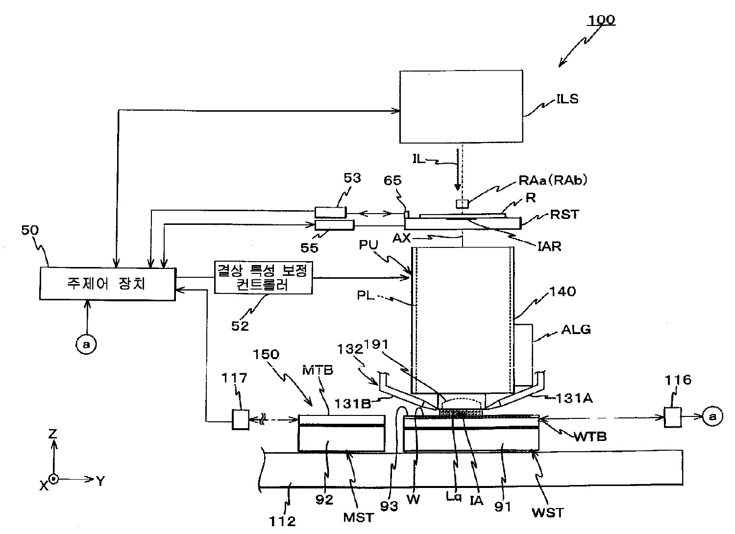
도 1에는 일 실시형태에 따른 노광 장치(100)의 구성이 개략적으로 나타내어져 있다. 이 노광 장치(100)는 스텝·앤드·스캔 방식의 주사형 노광 장치, 즉 소위 스캐너이다. FIG. 1 schematically shows the structure of an
노광 장치(100)는, 조명계(ILS), 이 조명계(ILS)로부터의 에너지 빔으로서의 노광용 조명 광(IL)에 의해 조명되는 마스크로서의 레티클(R)을 유지하여 정해진 주사 방향(여기서는, 도 1에 있어서의 지면 내 좌우 방향인 Y축 방향으로 함)으로 이동하는 레티클 스테이지(RST), 레티클(R)로부터 사출된 노광용 조명 광(IL)을 웨이퍼(W) 상에 투사하는 투영 광학계(PL)를 포함하는 투영 유닛(PU), 웨이퍼(W)가 적재되는 물체 스테이지로서의 웨이퍼 스테이지(WST) 및 노광을 위한 계측에 이용되는 계측 스테이지(MST)를 포함하는 스테이지 장치(150) 및 이들의 제어계 등을 갖추고 있다. The
조명계(ILS)에 탑재된 광원으로서는, 일례로서 파장 200 nm~170 nm의 진공 자외역의 광을 발하는 펄스 광원인 ArF 엑시머 레이저 광원(출력 파장 193 nm)이 이용되고 있다. As a light source mounted in the illumination system ILS, the ArF excimer laser light source (output wavelength 193 nm) which is a pulsed light source which emits the light of the vacuum ultraviolet region of wavelength 200nm-170nm is used as an example.
또한, 조명계(ILS)는, 정해진 위치 관계로 배치된, 빔 정형 광학계, 에너지 세기 조절기, 옵티컬 인테그레이터(유니포마이저, 또는 호모지나이저), 조명계 개구 조절판, 광 분할기, 릴레이 렌즈, 레티클 블라인드, 광로 절곡용의 미러 및 콘덴서 렌즈(모두 도시되지 않음) 등을 포함하고 있다. 한편, 조명계(ILS)의 구성이나 각 광학 부재의 기능 등에 관해서는, 예컨대 국제 공개 제2002/103766호 팜플렛 등에 개시되어 있다. In addition, the illumination system ILS includes a beam shaping optical system, an energy intensity controller, an optical integrator (uniformizer or homogenizer), an illumination system aperture control plate, a light splitter, a relay lens, and a reticle blind, which are arranged in a predetermined positional relationship. And a mirror for condensing the optical path and a condenser lens (both not shown). On the other hand, the structure of an illumination system ILS, the function of each optical member, etc. are disclosed by the international publication 2002/103766 pamphlet etc., for example.
상기 레티클 스테이지(RST) 상에는, 회로 패턴 등이 그 패턴면(도 1에 있어서의 하면)에 형성된 레티클(R)이, 예컨대 진공 흡착에 의해 고정되어 있다. 레티클 스테이지(RST)는, 예컨대 리니어 모터 등을 포함하는 레티클 스테이지 구동계(55)에 의해서 XY 평면 내에서 미소 구동할 수 있고, 정해진 주사 방향(여기서는 도 1에 있어서의 지면 내 좌우 방향인 Y축 방향)으로 지정된 주사 속도로 구동할 수 있게 되어 있다.On the said reticle stage RST, the reticle R in which a circuit pattern etc. were formed in the pattern surface (lower surface in FIG. 1) is fixed by vacuum suction, for example. The reticle stage RST can be minutely driven in the XY plane by, for example, a reticle
레티클 스테이지(RST)의 스테이지 이동면 내의 위치(Z축 둘레의 회전을 포함함)는, 레티클 레이저 간섭계(이하, 「레티클 간섭계」라고 함)(53)에 의해서, 이동 거울(65)(실제로는, Y축 방향으로 직교하는 반사면을 갖는 Y 이동 거울과 X축 방향으로 직교하는 반사면을 갖는 X 이동 거울이 설치되어 있음)을 통해, 예컨대 0.5~1 nm 정도의 분해능으로 항상 검출된다. 이 레티클 간섭계(53)의 계측치는, 주제어 장치(50)에 보내지고, 주제어 장치(50)에서는, 이 레티클 간섭계(53)의 계측치에 기초하여 레티클 스테이지 구동계(55)를 통해 레티클 스테이지(RST)의 X축 방향, Y축 방향 및 θz 방향(Z축 둘레의 회전 방향)의 위치(및 속도)를 제어한다. The position (including rotation around the Z axis) of the reticle stage RST in the stage moving surface is moved mirror 65 (actually referred to as a "reticle interferometer") 53 by a moving mirror 65 (actually, A Y moving mirror having a reflective surface orthogonal to the Y axis direction and an X moving mirror having a reflective surface orthogonal to the X axis direction) are always detected, for example, with a resolution of about 0.5 to 1 nm. The measured value of the
레티클(R)의 위쪽에는, 투영 광학계(PL)를 통해 레티클(R) 상의 1쌍의 레티클 얼라인먼트 마크와 이들에 대응하는 계측 스테이지(MST) 상에 설치된 기준 마크판(FM)(도 2 등 참조) 위의 1쌍의 기준 마크(이하, 「제1 기준 마크」라고 함)를 동시에 관찰하기 위한 노광 파장의 광을 이용한 TTR(Through The Reticle) 얼라인먼트계로 이루어지는 1쌍의 레티클 얼라인먼트 검출계(RAa, RAb)가 X축 방향으로 소정 거리 떨어져 설치되고 있다. 이들 레티클 얼라인먼트 검출계(RAa, RAb)로서는, 예컨대 일본 특허 공개 평7-176468호 공보 및 이것에 대응하는 미국 특허 제5,646,413호 명세서 등에 개시되는 것과 같은 구성의 것이 이용되고 있다. 본 국제 출원에서 지정한 지정국(또는 선택한 선택국)의 국내 법령이 허용하는 한도에서, 상기 공보 및 미국 특허에 있어서의 개시를 원용하여 본 명세서의 기재의 일부로 한다. Above the reticle R, a pair of reticle alignment marks on the reticle R and a reference mark plate FM provided on the corresponding measurement stage MST through the projection optical system PL (see FIG. 2 and the like). ) A pair of reticle alignment detection systems (RAa) comprising a TTR (Through The Reticle) alignment system using light of an exposure wavelength for simultaneously observing the pair of reference marks (hereinafter referred to as "first reference marks"). RAb) is provided a predetermined distance away in the X-axis direction. As these reticle alignment detection systems RAa and RAb, the thing of the structure as disclosed, for example by Unexamined-Japanese-Patent No. 7-176468, the specification of US Patent No. 5,646, 413, etc. is used. To the extent permitted by national legislation of the designated country (or selected selected country) specified in this international application, the disclosures in this publication and US patents are incorporated herein by reference.
상기 투영 유닛(PU)은, 도 1에 있어서 레티클 스테이지(RST)의 아래쪽에 배치되어 있다. 투영 유닛(PU)은, 경통(140)과, 이 경통(140) 내에 정해진 위치 관계로 유지된 복수의 광학 소자로 이루어지는 투영 광학계(PL)를 포함한다. 투영 광학계(PL)로서는, 예컨대 Z축 방향의 공통의 광축(AX)을 갖는 복수의 렌즈(렌즈 엘리멘트)로 이루어지는 굴절 광학계가 이용되고 있다. 이 투영 광학계(PL)는, 예컨대 양측 텔레센트릭으로 정해진 투영 배율(예컨대 1/4배, 1/5배 또는 1/8배)을 갖는다. 이 때문에, 조명 광학계(12)로부터의 조명 광(IL)에 의해서 레티클(R) 상의 조명 영역(IAR)이 조명되면, 이 레티클(R)을 통과한 조명 광(IL)에 의해, 투영 광학계(PL)(투영 유닛(PU))를 통해 그 조명 영역(IAR) 내의 레티클(R)의 회로 패턴의 축소상(회로 패턴의 일부의 축소상)이 표면에 레지스트(감응재)가 도포된 웨이퍼(W) 상의 상기 조명 영역(IAR)에 공역인 영역(이하, 「노광 영역」이라고도 함)(IA)에 형성된다. 한편, 본 실시형태에 있어서, 투영 광학계(PL)를 구성하는 가장 상면(像面) 측(웨이퍼 측)의 종단 광학 소자(191)는 굴절력을 갖는 렌즈이지만, 굴절력이 없는 평행 평면판이라도 좋다. The projection unit PU is disposed below the reticle stage RST in FIG. 1. The projection unit PU includes the
또한, 투영 광학계(PL)를 구성하는 복수의 렌즈 중, 특정한 복수의 렌즈는, 주제어 장치(50)로부터의 지령에 기초하여, 결상 특성 보정 컨트롤러(52)에 의해서 제어되어, 투영 광학계(PL)의 광학 특성(결상 특성을 포함함), 예컨대 배율, 디스토션, 코마 수차 및 상면 만곡(상면 경사를 포함함) 등을 조정할 수 있다. Moreover, of the some lens which comprises the projection optical system PL, the specific some lens is controlled by the imaging
한편, 본 실시형태의 노광 장치(100)에서는, 후술하는 바와 같이 액침법을 적용한 노광이 이루어지기 때문에, 개구수(NA)가 실질적으로 증대함에 따라서 레티클 측의 개구가 커진다. 이 때문에, 렌즈만으로 구성되는 굴절 광학계에서는, 페츠발(Petzval)의 조건을 만족하는 것이 곤란하게 되어, 투영 광학계가 대형화되는 경향에 있다. 이러한 투영 광학계의 대형화를 피하기 위해서, 미러와 렌즈를 포함하는 반사 굴절계(카타디옵트릭(catadioptric)계)를 이용하더라도 좋다. On the other hand, in the
또한, 본 실시형태의 노광 장치(100)에서는, 투영 광학계(PL)를 구성하는 가장 상면 측(웨이퍼(W) 측)의 종단 광학 소자인 렌즈(이하, 「선단 렌즈」라고도 함)(191)의 근방에는, 액침 장치(132)의 일부를 구성하는 액체 공급 노즐(131A)과, 액체 회수 노즐(131B)이 설치되어 있다. Moreover, in the
상기 액체 공급 노즐(131A)에는, 그 일단이 액체 공급 장치(138)(도 1에서는 도시되지 않음, 도 6 참조)의 일부에 접속된 공급관(78)(도 1, 도 6에서는 도시되지 않음, 도 3 참조)의 타단이 접속되어 있고, 상기 액체 회수 노즐(131B)에는, 그 일단이 액체 회수 장치(139)(도 1에서는 도시되지 않음, 도 6 참조)에 접속된 도시되지 않는 회수관의 타단이 접속되어 있다. In the
본 실시형태에서는, 액침용의 액체(Lq)(도 1 참조)는, ArF 엑시머 레이저광(파장 193 nm의 광)이 투과하는 순수를 사용하여 만드는 것으로 한다. 순수는, 반도체 제조 공장 등에서 용이하게 대량으로 입수할 수 있고, 웨이퍼(W) 상의 레지스트 및 광학 렌즈 등에 대한 악영향이 적다는 이점이 있다. In the present embodiment, the liquid Lq (see FIG. 1) for immersion is made using pure water transmitted by ArF excimer laser light (wavelength of 193 nm). Pure water can be easily obtained in large quantities in a semiconductor manufacturing plant or the like, and has an advantage that the adverse effects on the resist on the wafer W, the optical lens, and the like are small.
도 3에는, 액체 공급 장치(138) 구성의 일례가 나타내어져 있다. 이 도 3에 도시된 바와 같이, 액체 공급 장치(138)는, 일단이 반도체 제조 공장의 순수의 공장 배관에 접속되고, 타단이 액체의 탱크를 겸하는 CO2 용해조(82)의 일단에 접속된 순수 공급관(84), 이 순수 공급관(84)의 도중에 설치된 유량 제어용 전자 밸브(86A), 상기 CO2 용해조(82)의 일단과 도시되지 않는 CO2 탱크를 접속하는 CO2 공급관(88), 이 CO2 공급관(88)의 도중에 설치된 유량 제어용 전자 밸브(86B), 상기 CO2 용해조(82)의 타단(순수 공급관(84)과는 반대측)에 그 일단이 접속된 공급 배관(90), 이 공급 배관(90)의 타단에 그 일단이 접속되어, 액체의 온도 조정을 하는 액체 온도 조정 기구(72), 상기 공급 배관(90)의 도중에 설치된 가압 펌프(74) 및 비저항계(76), 상기 액체 온도 조정 기구(72)의 타단측에 그 일단이 접속되고, 타단에 액체 공급 노즐(131A)이 설치된 공급관(78), 및 액체 온도 조정 기구(72), 유량 제어용 전자 밸브(86A, 86B), 가압 펌프(74), 비저항계(76) 등이 접속된 컨트롤러(80) 등을 갖추고 있다. An example of the structure of the
컨트롤러(80)는, 가압 펌프(74)를 주제어 장치(50)로부터의 지시에 기초하여 작동시키고, 그 작동 중에, 비저항계(76)에서 계측되는 CO2 용해조(82)로부터의 액체(이산화탄소가 용해된 순수)의 비저항치를 모니터하면서, 그 계측되는 비저항치가 소정 범위 내의 값이 되도록 유량 제어용 전자 밸브(86A, 86B)를 제어한다. 이에 따라, CO2 용해조(82)의 내부에서, 공장 배관을 통해 공급된 순수 중에 CO2 탱크로부터 공급된 이산화탄소(CO2)가 혼입되고 용해되어, 원하는 비저항치의 액체(순수, 엄밀히 말하면 탄산수)(Lq)가 생성된다. 즉, 본 실시형태에서는, 순수에 비저항을 저하시키는 이산화탄소를 혼입하여 용해시켜, 액체 공급 노즐(131A)을 통해 계측 테이블(MTB) 상 또는 웨이퍼 테이블(WTB) 상에 액체(Lq)로서 공급한다. 한편, 순수 중에 이산화탄소(탄산 가스)를 혼입(용해)하는 것은, 순수 중에 탄산 가스를 직접 주입하는 방식, 또는 중공사막(中空絲幕)을 통해 순수 중에 이산화탄소를 혼입시키는 방식 등, 각종 방식을 채용할 수 있다. 한편, 이산화탄소를 포함하는 공기를 순수 중에 용해시키더라도 좋다. The
그리고, 컨트롤러(80)의 지시 하에, 액체 온도 조정 기구(72)에 의해 그 액체(Lq)의 온도가, 노광 장치 본체가 수납되어 있는 챔버(도시되지 않음) 안의 온도와 같은 정도의 온도로 조정된다. 여기서, 컨트롤러(80)는, 순수와 이산화탄소와의 유량의 비를 유지한 상태에서, 유량 제어용 전자 밸브(86A, 86B)의 개방도를 조정함으로써, 액체 공급 노즐(131A)을 통해 공급되는 액체(Lq)의 유량을 조정한다. 단, 액체 온도 조정 기구(72)의 내부 또는 그 근방에 유량 제어 밸브를 설치하여, 액체의 온도와 유량을 조정하도록 하더라도 물론 좋다. Then, under the instruction of the
상기 액체 회수 장치(139)는, 액체의 탱크와 흡인 펌프, 및 회수관을 통한 액체의 회수·정지를 제어하기 위한 밸브 등을 포함한다. 밸브로서는, 전술한 액체 공급 장치(138) 측의 밸브에 대응하여 유량 제어 밸브를 이용하는 것이 바람직하다. The
ArF 엑시머 레이저광에 대한 순수의 굴절율 n은 거의 1.44이다. 이 순수 중에서는, 조명 광(IL)의 파장은 193 nm×1/n=약 134 nm로 단파장(短波長)화된다. 본 실시형태의 경우, 액체(Lq)로서 전술한 이산화탄소가 용해된 수용액이 이용되기 때문에, 엄밀하게 말하면, 그 혼입된 이산화탄소의 비율에 따라 순수와 굴절율이 다르지만, 이산화탄소의 혼입 비율은 작기 때문에 ArF 엑시머 레이저광에 대한 액체(Lq)의 굴절율은 전술한 값과 그다지 다르지 않은 것으로 한다. The refractive index n of pure water for an ArF excimer laser light is almost 1.44. In this pure water, the wavelength of the illumination light IL is shortened to 193 nm x 1 / n = about 134 nm. In the case of the present embodiment, since the above-described aqueous solution in which carbon dioxide is dissolved is used as the liquid Lq, strictly speaking, the pure water and the refractive index differ depending on the ratio of the incorporated carbon dioxide, but since the mixing ratio of carbon dioxide is small, the ArF excimer It is assumed that the refractive index of the liquid Lq with respect to the laser light is not very different from the above-described values.
상기 액체 공급 노즐(131A)과 상기 액체 회수 노즐(131B)을 포함하는 액침 장치(132)는 주제어 장치(50)에 의해서 제어된다(도 6 참조). 주제어 장치(50)는, 액체 공급 노즐(131A)을 통해 선단 렌즈(191)와 웨이퍼(W)와의 사이에 액체(Lq)를 공급하고, 액체 회수 노즐(131B)을 통해 선단 렌즈(191)와 웨이퍼(W)와의 사이에서 액체(Lq)를 회수한다. 이 때, 주제어 장치(50)는, 선단 렌즈(191)와 웨이퍼(W)와의 사이에 액체 공급 노즐(131A)로부터 공급되는 액체(Lq)의 양과, 액체 회수 노즐(131B)을 통해 회수되는 액체(Lq)의 양이 항상 같게 되도록 제어하고 있다. 따라서, 선단 렌즈(191)와 웨이퍼(W)와의 사이에, 일정량의 액체(Lq)(도 1 참조)가 유지된다. 이 경우, 선단 렌즈(191)와 웨이퍼(W)와의 사이에 유지된 액체(Lq)는 항상 교체되고 있다. The
한편, 투영 유닛(PU) 아래쪽에 계측 스테이지(MST)가 위치하는 경우에도, 상기와 같은 식으로 계측 테이블(MTB)과 선단 렌즈(191)와의 사이에 액체(Lq)를 채우는 것이 가능하다. On the other hand, even when the measurement stage MST is positioned below the projection unit PU, it is possible to fill the liquid Lq between the measurement table MTB and the tip lens 191 in the same manner as described above.
한편, 전술한 설명에서는, 그 설명을 간단하게 하기 위해서 액체 공급 노즐과 액체 회수 노즐이 각각 하나씩 설치되어 있는 것으로 했지만, 이에 한하지 않고, 예컨대, 국제 공개 제99/49504호 팜플렛에 개시되는 것과 같이, 노즐을 다수 갖는 구성을 채용하는 것으로 하여도 좋다. 또한, 액침 장치(132)에, 유럽 특허 출원 공개 제1,598,855호 공보 또는 국제 공개 제2004/090634호 팜플렛 등에 개시되어 있는 구성을 채용할 수도 있다. 요는, 투영 광학계(PL)를 구성하는 최하단의 광학 부재(선단 렌즈)(191)와 웨이퍼(W)와의 사이에 액체를 공급할 수 있는 것이면, 액침 장치(132)의 구성은 어떠한 것이라도 좋다. In addition, in the above description, in order to simplify the description, the liquid supply nozzles and the liquid recovery nozzles are provided one by one, but not limited thereto. For example, as disclosed in the pamphlet of International Publication No. 99/49504 In addition, you may employ | adopt the structure which has many nozzles. The
상기 투영 유닛(PU)의 +Y측에는, 도 1에 도시된 바와 같이, 웨이퍼(W) 상의 얼라인먼트 마크 등의 검출 대상 마크를 광학적으로 검출하는 오프-액시스·얼라인먼트계(이하, 「얼라인먼트계」라고 약칭함)(ALG)가 설치되어 있다. 한편, 얼라인먼트계(ALG)로서는, 각종 방식의 센서를 이용할 수 있지만, 본 실시형태에 있어서는, 화상 처리 방식의 센서가 이용되고 있다. 한편, 화상 처리 방식의 센서는, 예컨대 일본 특허 공개 평4-65603호 공보 및 이것에 대응하는 미국 특허 제5,493,403호 명세서 등에 개시되어 있다. 얼라인먼트계(ALG)로부터의 촬상 신호는 주제어 장치(50)에 공급된다(도 6 참조). 본 국제 출원에서 지정한 지정국(또는 선택한 선택국)의 국내 법령이 허용하는 한도에서, 상기 공보 및 미국 특허에 있어서의 개시를 원용하여 본 명세서의 기재의 일부로 한다. On the + Y side of the projection unit PU, as shown in FIG. 1, an off-axis alignment system (hereinafter referred to as "alignment system") that optically detects a target to be detected, such as an alignment mark on the wafer W, is referred to. Abbreviated) (ALG) is installed. In addition, although the sensor of various systems can be used as alignment system ALG, in this embodiment, the sensor of an image processing system is used. On the other hand, an image processing sensor is disclosed in, for example, Japanese Unexamined Patent Publication No. Hei 4-65603 and US Pat. No. 5,493,403 corresponding thereto. The imaging signal from the alignment system ALG is supplied to the main controller 50 (see FIG. 6). To the extent permitted by national legislation of the designated country (or selected selected country) specified in this international application, the disclosures in this publication and US patents are incorporated herein by reference.
도 1 및 도 2에 도시된 바와 같이, 상기 스테이지 장치(150)는, 베이스반(盤)(112)과, 이 베이스반(112)의 상면의 위쪽에 배치된 웨이퍼 스테이지(WST) 및 계측 스테이지(MST)와, 이들 스테이지(WST, MST)의 위치를 계측하는 간섭계 시스템(118)(도 6 참조)과, 리니어 모터 등을 사용하여 스테이지(WST, MST)를 구동하는 스테이지 구동계(124)(도 6 참조)를 포함하고 있다. As shown in FIG. 1 and FIG. 2, the
웨이퍼 스테이지(WST) 및 계측 스테이지(MST)의 저면에는, 도시되지 않는 비접촉 베어링, 예컨대 공기 정압 베어링(즉, 에어 베어링(에어 패드라고도 불림))이 여러 곳에 설치되어 있고, 이들 공기 정압 베어링으로부터 베이스반(112)의 상면으로 향해서 분출된 가압 공기의 정압에 의해, 베이스반(112)의 상면의 위쪽에 웨이퍼 스테이지(WST), 계측 스테이지(MST)가 수 μm 정도의 클리어런스를 통해 부상 지지되어 있다. 또한, 스테이지(WST, MST)의 각각은 스테이지 구동계(124)에 의해서, XY 면내에서 상호 독립적으로 구동(θz 회전을 포함함)된다. 웨이퍼 스테이지(WST), 및 계측 스테이지(MST)의 스테이지 이동면(XY 평면) 내의 위치, 및 각 좌표 축 둘레의 회전 위치는 간섭계 시스템(118)에 의해 검출된다. 한편, 도 1에 있어서는, 설명을 간단하게 하기 위해서, 웨이퍼 스테이지(WST)의 Y축 방향의 위치를 계측하기 위한 Y축 간섭계(116), 계측 스테이지(MST)의 Y축 방향의 위치를 계측하기 위한 Y축 간섭계(117)만이 도시되어 있다. 간섭계 시스템(118)(116, 117)의 계측치는 주제어 장치(50)에 보내지고, 주제어 장치(50)는 간섭계 시스템(118)의 계측치에 기초하여 스테이지 구동계(124)를 통해 웨이퍼 스테이지(WST) 및 계측 스테이지(MST)의 위치(및 속도)를 제어한다. On the bottom surfaces of the wafer stage WST and the measurement stage MST, non-illuminated bearings (not shown) such as air static pressure bearings (i.e., air bearings (also called air pads)) are provided in various places, and the bases are formed from these air static pressure bearings. By the positive pressure of the pressurized air blown toward the upper surface of the
이것을 더욱 상세히 설명하면, 웨이퍼 스테이지(WST)는, 도 1에 도시된 바와 같이, 상기 에어 베어링이 그 저면에 설치된 웨이퍼 스테이지 본체(91)와, 이 웨이퍼 스테이지 본체(91) 상에 도시되지 않는 Z·레벨링 기구(예컨대 보이스 코일 모터 등의 액츄에이터를 포함하고 있음)를 통해 탑재되어, 웨이퍼 스테이지 본체(91)에 대하여 Z축 방향, X축 둘레의 회전 방향(θx 방향) 및 Y축 둘레의 회전 방향(θy 방향)으로 미소 구동되는 웨이퍼 테이블(WTB)을 포함하고 있다. In more detail, the wafer stage WST has a wafer stage
웨이퍼 테이블(WTB) 상에는, 웨이퍼(W)를 진공 흡착 등에 의해서 유지하는 웨이퍼 홀더(도시되지 않음)가 설치되어 있다. 이 웨이퍼 홀더는, 판형의 본체부와, 이 본체부의 상면에 고정되고 그 중앙에 웨이퍼(W)의 직경보다 0.1~2 mm 정도 직경이 큰 원형 개구가 형성된 플레이트(93)(도 1, 도 2 참조)를 구비하고 있다. 플레이트(93)의 원형 개구 내부의 본체부의 영역에는 다수의 핀이 배치되어 있고, 그 다수의 핀에 의해서 웨이퍼(W)가 지지된 상태로 진공 흡착되어 있다. 이 경우, 웨이퍼(W)가 진공 흡착된 상태에서는, 그 웨이퍼(W) 표면과 플레이트(93)의 표면이 거의 동일한 높이가 된다. 플레이트(93) 전면의 표면에 불소계 수지 재료나 아크릴계 수지 재료 등의 발액성 재료(발수 재료)가 코팅되어, 발액막이 형성되고 있다. 또한, 웨이퍼(W)의 표면에는, 레지스트(감응재)가 도포되어, 그 도포된 레지스트에 의해 레지스트막이 형성되어 있다. 이 경우, 레지스트막은 액침용의 액체(Lq)에 대하여 발액성인 것을 이용하는 것이 바람직하다. 또한, 웨이퍼(W)의 표면에 그 레지스트막을 덮도록 탑코팅막(층)을 형성하더라도 좋다. 이 탑코팅막으로서 액침용의 액체(Lq)에 대하여 발액성인 것을 이용하는 것이 바람직하다. 한편, 탑코팅막은, 액체(Lq)로부터 레지스트막을 보호하는 보호 기능, 레지스트막을 구성하는 물질의 액체(Lq)에의 용출을 방지하는 용출 방지 기능, 및 조명 광(IL)의 반사를 방지하는 반사 방지 기능의 적어도 하나를 갖고 있다. On the wafer table WTB, a wafer holder (not shown) for holding the wafer W by vacuum suction or the like is provided. This wafer holder is plate 93 (FIG. 1, FIG. 2) formed with the plate-shaped main-body part and the circular opening which is fixed to the upper surface of this main-body part, and whose diameter is 0.1-2 mm larger than the diameter of the wafer W in the center. Reference). A large number of fins are arranged in the region of the body portion inside the circular opening of the
상기 계측 스테이지(MST)는 도 1에 도시된 바와 같이, 상기 에어 베어링이 그 저면에 설치된 계측 스테이지 본체(92)와, 이 계측 스테이지 본체(92) 상에 도시되지 않는 Z·레벨링 기구를 통해 탑재된 계측 테이블(MTB)을 구비하고 있다. As shown in FIG. 1, the measurement stage MST is mounted via a measurement stage
계측 테이블(MTB)은, 상면이 개구된 중공 직방체형의 케이스체(120)(도 5 참조)와, 이 케이스체(120)의 상면을 폐색(閉塞)하는 예컨대 폴리4불화에틸렌(테플론(등록 상표)) 등의 발액성을 갖는 재료에 의해서 형성되는 소정 두께의 플레이트 부재(101)를 포함하며, 높이 방향의 치수가 폭 방향 및 깊이 방향의 치수에 비해서 현저히 작은 직방체형의 외견을 갖고 있다. The measurement table MTB includes a hollow rectangular parallelepiped case body 120 (see FIG. 5) having an open upper surface, and a polytetrafluoroethylene (teflon (registration) that closes the upper surface of the case body 120. A
상기 플레이트 부재(101)는, 계측 테이블(MTB)의 평면도인 도 4에 도시된 바와 같이, Y축 방향을 길이 방향으로 하는 장방형의 개구(101a), 이 개구(101a)와 거의 동일한 X축 방향 치수를 지니고 그 X축 방향을 길이 방향으로 하는 장방형의 개구(101b)와, 3개의 원형 개구(101d, 101e, 101f)가 형성되어 있다. As shown in FIG. 4 which is the top view of the measurement table MTB, the said
상기 플레이트 부재(101)의 개구(101b)의 내측 및 개구(101b) 아래쪽의 케이스체(120)의 내부에는, 도 5에 도시된 바와 같이 조도 모니터(조사량 모니터)(122)가 배치되어 있다. 이 조도 모니터(122)는 도 5에 도시된 바와 같이, 합성 석영 또는 형석 등을 소재로 하는 유리로 이루어지는 유리 부재(126), 및 이 유리 부재(126)의 하면에 거의 간극 없이 고정된 광 센서(128) 등을 갖추고 있다. 광 센서(128)는 도 5에 나타내어지는 전술한 노광 영역(IA)(도 4 참조)에 조사된 조명 광(IL)의 거의 전부를 수광할 수 있을 정도의 소정 면적의 수광면을 구비하고, 조명 광(IL)과 동일한 파장 영역(예컨대 파장 300 nm~100 nm 정도)에서 감도가 있으며, 또한 조명 광(IL)을 검출하기 위해서 높은 응답 주파수를 갖는 복수의 실리콘·포토·다이오드(또는 포토·멀티플라이어·튜브) 등의 수광 소자군을 포함하고 있다. An illuminance monitor (irradiation monitor) 122 is disposed inside the
유리 부재(126)는 도 5에 도시된 바와 같이, 플레이트 부재(101)의 개구(101b) 부분의 내측면 및 하측면에 대하여 정해진 갭을 통해 대향하는 형상을 갖고 있다. 이 경우, 개구(101b)와 유리 부재(126)의 상부 측면과의 사이의 갭(B)의 폭 치수는 예컨대 0.3 mm 정도로 설정되고 있다. As shown in FIG. 5, the
유리 부재(126)는, 케이스체(120)의 저벽의 상면에 설치된 지지 부재(130)에 위쪽에서부터 결합하고 있다. 즉, 지지 부재(130)는, 광 센서(128)를 둘러싸는 평면에서 보아(위쪽에서부터 보아) 소정 폭의 프레임형의 형상을 갖고 있고, 유리 부재(126)의 하면의 외연부에는 지지 부재(130)의 상단부에 결합하는 단부가 형성되어 있다. 유리 부재(126)에는, 그 상면에 조명 광(IL)을 감광하는 크롬 등의 금속 박막으로 이루어지는 감광막(129)이 전면에 걸쳐 형성되고, 또한 그 감광막의 상부에 불소계 수지 재료, 또는 아크릴계 수지 재료 등의 발액성 재료(발수 재료)가 코팅되며, 이로써 발액막(WRF)이 형성되어 있다. 본 실시형태에서는, 이 발액막(WRF)의 상면과 플레이트 부재(101)의 상면은 거의 동일면(면일)으로 설정되고 있다. The
한편, 유리 부재(126) 하면에는 중앙부의 장방형 영역을 제외한 영역에 크롬 등의 금속막으로 이루어지는 차광막(127)이 형성되어 있다. 이 차광막(127)에 의해, 도 5에 도시된 바와 같이 갭(B) 부분을 통해 유리 부재(126)에 입사한 미광(迷光)(도 5 중의 굵은 선의 실선 화살표 참조)이 컷트(차광)된다. On the other hand, the
본 실시형태의 조도 모니터(122)는, 예컨대 일본 특허 공개 평6-291016호 공보 및 이것에 대응하는 미국 특허 제5,721,608호 명세서 등에 개시되는 조도 모니터(조사량 모니터)와 같은 구성을 갖고 있으며, 투영 광학계(PL)의 상면 상에서 액체(Lq)를 통해 조명 광(IL)의 조도를 계측한다. 조도 모니터(122)의 일부를 구성하는 광 센서(128)의 검출 신호(광전 변환 신호)가 도시되지 않는 홀드 회로(예컨대 피크 홀드 회로 등) 및 아날로그/디지털(A/D) 변환기를 통해 주제어 장치(50)에 공급되고 있다. 본 국제 출원에서 지정한 지정국(또는 선택한 선택국)의 국내 법령이 허용하는 한도에서, 상기 공보 및 미국 특허에 있어서의 개시를 원용하여 본 명세서의 기재의 일부로 한다. The illuminance monitor 122 of this embodiment has a structure similar to the illuminance monitor (irradiation monitor) disclosed, for example in Unexamined-Japanese-Patent No. 6-291016, US Patent No. 5,721,608, etc., and a projection optical system The illuminance of the illumination light IL is measured through the liquid Lq on the upper surface of the PL. The main control unit is provided with a detection circuit (photoelectric conversion signal) of the
한편, 유리 부재(126)의 측면의 적어도 플레이트 부재(101)에 대향하는 영역, 및 플레이트 부재(101)의 유리 부재(126)에 대향하는 개구(101b)의 내벽면은, 발액 처리되어 발액성으로 되고 있다. 발액 처리로서는, 전술한 불소계 수지 재료 또는 아크릴계 수지 재료 등의 발액성 재료를 도포하는 것 등으로 행할 수 있다. On the other hand, the inner wall surface of the area | region which opposes at least the
또한, 케이스체(120) 저벽에는, 전술한 지지 부재(130)의 근방에, 배출 구멍(120a)이 형성되어 있고, 이 배출 구멍(120a)은 도시되지 않는 배관을 통해 도시되지 않는 회수부에 접속되어 있다. 이 회수부는, 진공계 및 액체(Lq)를 수용할 수 있는 탱크를 포함하는 기액 분리기 등을 갖추고 있다. 전술한 발액 처리에도 불구하고, 갭(B)을 통해 케이스체(120)의 내부에 유입한 액체(Lq)는 그 회수부에서 회수된다. Moreover, the
상기 플레이트 부재(101)의 개구(101a)의 내부에는, 도 4에 도시된 바와 같이, 평면에서 보아 장방형의 기준 마크판(FM)이 배치되어 있다. 이 경우, 기준 마크판(FM)과 플레이트 부재(101)와의 사이에는 예컨대 0.3 mm 정도의 갭(A)이 기준 마크판(FM)의 주위에 형성되어 있다. 기준 마크판(FM)의 상면은 플레이트 부재(101) 표면과 거의 동일한 높이(동일면)로 설정되고 있다. 이 기준 마크판(FM)의 표면에는, 전술힌 1쌍의 레티클 얼라인먼트 검출계(RAa, RAb)에 의해서 1쌍씩 동시 계측이 가능한 3쌍의 제1 기준 마크(RM11~RM32)와, 얼라인먼트계(ALG)에 의해 검출되는 3개의 제2 기준 마크(WM1~WM3)가 정해진 위치 관계로 형성되어 있다. 이들 기준 마크의 각각은, 기준 마크판(FM)을 구성하는 부재(예컨대 극저 팽창 유리 세라믹, 예컨대 클리어세럼(등록 상표) 등)의 표면에 거의 전면에 걸쳐 형성된 크롬층에 상기 정해진 위치 관계로 패터닝에 의해 형성된 개구 패턴에 의해서 형성되어 있다. 한편, 각 기준 마크를 알루미늄 등의 패턴(남기기 패턴)에 의해서 형성하더라도 좋다. In the inside of the
본 실시형태에서는, 예컨대 일본 특허 공개 평5-21314호 공보 및 이것에 대응하는 미국 특허 제5,243,195호 명세서 등에 개시되는 것과 같이, 상기 제1 기준 마크 (RMj1, RMj2(j=1~3))는, 액체(Lq)를 통해 전술한 1쌍의 레티클 얼라인먼트 검출계(RAa, RAb)에 의해서 동시에 계측 가능하고, 또한 이 제1 기준 마크(RMj1, RMj2)의 계측과 동시에 제2 기준 마크(WMj)를 액체(Lq)를 통하지 않고서 얼라인먼트계(ALG)에 의해서 계측할 수 있도록 상기 각 기준 마크의 배치가 정해지고 있다. 본 국제 출원에서 지정한 지정국(또는 선택한 선택국)의 국내 법령이 허용하는 한도에서, 상기 공보 및 미국 특허에 있어서의 개시를 원용하여 본 명세서의 기재의 일부로 한다. 또한, 기준 마크판(FM)의 상면은 거의 평탄면으로 되어 있고, 다점 초점 위치 검출계의 기준면으로서 이용하는 것으로 하여도 좋다. 이 기준 마크판(FM)의 상면에는, 도시하지 않기는 하지만, 전술한 크롬층의 상부에 전술한 불소계 수지 재료, 또는 아크릴계 수지 재료 등의 발액성 재료로 이루어지는 발액막이 형성되어 있다. In the present embodiment, the first reference marks RM j1 , RM j2 (j = 1 to 3) are disclosed, for example, as disclosed in Japanese Patent Laid-Open No. 5-21314 and the specification of US Patent No. 5,243,195 corresponding thereto. ) Can be simultaneously measured by the pair of reticle alignment detection systems RAa and RAb described above via the liquid Lq, and the second reference at the same time as the measurement of the first reference marks RM j1 and RM j2 . The arrangement of the respective reference marks is determined so that the mark WM j can be measured by the alignment system ALG without passing through the liquid Lq. To the extent permitted by national legislation of the designated country (or selected selected country) specified in this international application, the disclosures in this publication and US patents are incorporated herein by reference. The upper surface of the reference mark plate FM is almost a flat surface, and may be used as a reference surface of the multi-point focus position detection system. Although not shown, on the upper surface of the reference mark plate FM, a liquid-repellent film made of a liquid-repellent material such as the above-described fluorine resin material or acrylic resin material is formed on the above-mentioned chromium layer.
기준 마크판(FM)의 측면의 적어도 플레이트 부재(101)에 대향하는 영역 및 플레이트 부재(101)의 기준 마크판(FM)에 대향하는 개구(101a)의 내벽면은, 전술한 것과 같은 발액 처리가 실시되고 있다. 또한, 케이스체(120)의 저벽에는, 기준 마크판(FM)의 근방에도 전술한 배출 구멍(120a)과 같은 배출 구멍이 형성되고, 이 배출 구멍이 전술한 회수부의 진공계에 접속되어 있다. The inner wall surface of the area | region which opposes at least the
상기 플레이트 부재(101)의 개구(101d)의 내측 및 개구(101b) 아래쪽의 케이스체(120)의 내부에는, 평면에서 보아 원형의 패턴판(103)을 갖는 조도 불균일 계측기(104)가 배치되어 있다. 패턴판(103)과 플레이트 부재(101)와의 사이에는 예컨대 0.3 mm 정도의 폭 치수의 갭(D)이 패턴판(103)의 주위에 형성되어 있다. The roughness
조도 불균일 계측기(104)는, 상기 패턴판(103)과, 이 패턴판의 아래쪽에 배치된 도시되지 않는 수광 소자(전술한 실리콘·포토·다이오드 또는 포토·멀티플라이어·튜브 등)로 이루어지는 센서를 갖고 있다. 패턴판(103)은 전술한 유리 부재(126)와 마찬가지로 석영 유리 등으로 이루어지며, 그 표면에 크롬 등의 차광막이 성막되고, 이 차광막의 중앙에 광 투과부로서 핀 홀(103a)이 형성되어 있다. 그리고, 그 차광막 위에, 전술한 불소계 수지 재료, 또는 아크릴계 수지 재료 등의 발액성 재료로 이루어지는 발액막이 형성되어 있다. The illuminance
전술한 조도 불균일 계측기(104)는, 일본 특허 공개 소57-117238호 공보 및 이것에 대응하는 미국 특허 제4,465,368호 명세서 등에 개시되는 조도 불균일 계측기와 같은 구성을 갖고 있으며, 투영 광학계(PL)의 상면 상에서 액체(Lq)를 통해 조명 광(IL)의 조도 불균일을 계측한다. 그리고, 조도 불균일 계측기를 구성하는 센서의 검출 신호(광전 변환 신호)가 도시되지 않는 홀드 회로(예컨대 피크 홀드 회로 등), 및 아날로그/디지털(A/D) 변환기를 통해 주제어 장치(50)에 공급되고 있다. 본 국제 출원에서 지정한 지정국(또는 선택한 선택국)의 국내 법령이 허용하는 한도에서, 상기 공보 및 미국 특허에 있어서의 개시를 원용하여 본 명세서의 기재의 일부로 한다. The illuminance
상기 플레이트 부재(101)의 개구(101e)의 내부에는, 평면에서 보아 원형의 슬릿판(105)이, 그 표면이 플레이트 부재(101) 표면과 거의 동일면(면일)으로 되는 상태로 배치되어 있다. 슬릿판(105)과 플레이트 부재(101)와의 사이에는 예컨대 0.3 mm 정도 폭 치수의 갭(E)이, 슬릿판(105)의 주위에 형성되어 있다. 이 슬릿판(105)은, 전술한 패턴판(103)과 마찬가지로, 석영 유리와, 이 석영 유리의 표면에 형성된 크롬 등의 차광막을 구비하고, 이 차광막의 소정 부위에 X축 방향, Y축 방향으로 뻗는 슬릿 패턴이 광 투과부로서 형성되어 있다. 그리고, 그 차광막 위에, 전술한 불소계 수지 재료나 아크릴계 수지 재료 등의 발액성 재료로 이루어지는 발액막이 형성되어 있다. 이 슬릿판(105)은, 투영 광학계(PL)에 의해 투영되는 패턴의 공간상(투영상)의 광 강도를 계측하는 공간상 계측기의 일부를 구성하는 것이다. 본 실시형태에서는, 이 슬릿판(105)의 아래쪽의 계측 테이블(MTB)(케이스체(120))의 내부에는, 투영 광학계(PL) 및 액체(Lq)를 통해 플레이트 부재(101)에 조사되는 조명 광(IL)을, 상기 슬릿 패턴을 통해 수광하는 수광계가 설치되어 있고, 이에 의해서, 예컨대 일본 특허 공개 2002-14005호 공보 및 이것에 대응하는 미국 특허 출원 공개 제2002/0041377호 명세서 등에 개시되는 공간상 계측기와 같은 공간상 계측기가 구성되어 있다. 본 국제 출원에서 지정한 지정국(또는 선택한 선택국)의 국내 법령이 허용하는 한도에서, 상기 공보 및 미국 특허 출원 공개 명세서에 있어서의 개시를 원용하여 본 명세서의 기재의 일부로 한다. Inside the
상기 플레이트 부재(101)의 개구(101f)의 내부에는, 평면에서 보아 원형의 파면수차 계측용 패턴판(107)이, 그 표면이 플레이트 부재(101) 표면과 거의 동일면(면일)으로 되는 상태로 배치되어 있다. 이 파면수차 계측용 패턴판(107)은, 전술한 패턴판(103)과 마찬가지로, 석영 유리와, 이 석영 유리의 표면에 형성된 크롬 등의 차광막을 구비하고, 이 차광막의 중앙에 원형의 개구가 형성되어 있다. 그리고, 그 차광막 위에, 전술한 불소계 수지 재료, 또는 아크릴계 수지 재료 등의 발액성 재료로 이루어지는 발액막이 형성되어 있다. 이 파면수차 계측용 패턴판(107)의 아래쪽의 계측 테이블(MTB)(케이스체(120))의 내부에는, 투영 광학계(PL) 및 액체(Lq)를 통해 조명 광(IL)을 수광하는 예컨대 마이크로 렌즈 어레이를 포함하는 수광계가 설치되어 있고, 이에 의해서 예컨대 국제 공개 제99/60361호 팜플렛 및 이것에 대응하는 유럽 특허 제1,079,223호 명세서 등에 개시되는 파면수차 계측기가 구성되어 있다. 본 국제 출원에서 지정한 지정국(또는 선택한 선택국)의 국내 법령이 허용하는 한도에서, 상기 국제 공보 팜플렛 및 유럽 특허 명세서에 있어서의 개시를 원용하여 본 명세서의 기재의 일부로 한다. Inside the
전술한 패턴판(103), 슬릿판(105) 및 파면수차 계측용 패턴판(107) 각각의 측면의 적어도 플레이트 부재(101)에 각각 대향하는 영역, 및 플레이트 부재(101)의 패턴판(103)에 대향하는 개구(101d)의 내벽면, 슬릿판(105)에 대향하는 개구(101e)의 내벽면, 및 파면수차 계측용 패턴판(107)에 대향하는 개구(101f)의 내벽면 각각은 전술한 것과 같은 발액 처리가 이루어지고 있다. 또한, 케이스체(120)의 저벽에는, 패턴판(103)의 근방, 슬릿판(105)의 근방 및 파면수차 계측용 패턴판(107)의 근방에 전술한 배출 구멍(120a)과 같은 배출 구멍이 각각 형성되고, 이들 배출 구멍이 전술한 회수부의 진공계에 접속되어 있다. An area facing at least the
한편, 도시는 생략되어 있지만, 본 실시형태서는, 케이스체(120)의 내부에, 전술한 각종 계측기를 구성하는 수광 소자(센서)가 배치되어 있기 때문에, 이들 수광 소자의 발열의 영향을 최대한 피하도록, 이들의 수광 소자 및 케이스체(120)의 냉각 기구가 설치되어 있다. 수광 소자의 냉각 기구로서는, 예컨대 케이스체(120)의 저벽에 설치된 히트 싱크 및 이것에 접속된 펠티에 소자 조합 등을 들 수 있다. 또한, 케이스체(120) 그 자체의 냉각 기구로서는, 예컨대 배관계의 내부에 냉각액을 흘리는 액냉 방식의 기구를 채용할 수 있다. In addition, although illustration is abbreviate | omitted, in this embodiment, since the light receiving element (sensor) which comprises the above-mentioned various measuring instruments is arrange | positioned inside the case body 120, the influence of the heat_generation | fever of these light receiving elements is avoided as much as possible. Such a light receiving element and a cooling mechanism of the case body 120 are provided. As a cooling mechanism of a light receiving element, the heat sink provided in the bottom wall of the case body 120, the Peltier element combination connected to this, etc. are mentioned, for example. In addition, as the cooling mechanism of the case body 120 itself, for example, a liquid-cooling mechanism that flows a cooling liquid into the piping system can be adopted.
또, 열의 영향을 억제하는 관점에서, 전술한 공간상 계측기나 파면수차 계측기 등에서는, 예컨대 광학계 등의 일부만이 계측 스테이지(MST)에 탑재되어 있더라도 좋다. In addition, in view of suppressing the influence of heat, in the above-described spatial measuring instrument, wavefront aberration measuring instrument, or the like, only a part of the optical system or the like may be mounted in the measurement stage MST.
또한, 본 실시형태의 노광 장치(100)에서는, 도 1에서는 도시되어 있지 않지만, 조사계(110a) 및 수광계(110b)(도 6 참조)를 포함하는, 예컨대 일본 특허 공개 평6-283403호 공보(대응 미국 특허 제5,448,332호) 등에 개시되는 것과 같은 사입사(斜入射; Off-Axis Illumination) 방식의 다점 초점 위치 검출계가 설치되어 있다. In addition, in the
도 6에는 노광 장치(100)의 제어계의 주요한 구성이 나타내어져 있다. 이 제어계는, 장치 전체를 통괄적으로 제어하는 마이크로 컴퓨터(또는 워크스테이션)로 이루어지는 주제어 장치(50)를 중심으로 하여 구성되어 있다. 이 도 6에 있어서, 부호 143은 전술한 계측 테이블(MTB) 상에 설치된 조도 모니터(122), 조도 불균일 계측기(104), 공간상 계측기, 파면수차 계측기 등의 계측기군을 나타낸다. 6, the main structure of the control system of the
이어서, 본 실시형태의 노광 장치(100)에 있어서의, 웨이퍼 스테이지(WST)와 계측 스테이지(MST)를 이용한 병행 처리 동작에 관해서, 도 2 등에 기초하여 설명한다. 한편, 이하의 동작 중, 주제어 장치(50)가, 액침 장치(132)를 제어하여 투영 광학계(PL)의 선단 렌즈(191)의 바로 아래에 항상 액체(Lq)를 채우고 있다. Next, the parallel processing operation | movement which used the wafer stage WST and the measurement stage MST in the
도 2에는 웨이퍼 스테이지(WST) 상의 웨이퍼(W)(여기서는, 일례로서 어떤 로트(1 로트는 25장 또는 50장)의 최후의 웨이퍼로 함)에 대한 스텝·앤드·스캔 방식의 노광이 이루어지고 있는 상태가 나타내어져 있다. 이 때, 계측 스테이지(MST)는, 웨이퍼 스테이지(WST)와 충돌하지 않는 정해진 대기 위치에서 대기하고 있다. FIG. 2 is a step-and-scan exposure of the wafer W on the wafer stage WST (here, as an example, the last wafer of a certain lot (one lot is 25 or 50 sheets)). A state is shown. At this time, the measurement stage MST waits at a predetermined waiting position which does not collide with the wafer stage WST.
전술한 노광 동작은, 주제어 장치(50)에 의해, 사전에 이루어진 예컨대 엔핸스트·글로벌·얼라인먼트(EGA) 등의 웨이퍼 얼라인먼트의 결과 등에 기초하여, 웨이퍼(W) 상의 각 쇼트 영역의 노광을 위한 주사 시작 위치(가속 시작 위치)로 웨이퍼 스테이지(WST)가 이동되는 쇼트간 이동 동작과, 각 쇼트 영역에 대한 레티클(R)에 형성된 패턴을 주사 노광 방식으로 전사하는 주사 노광 동작을 반복함으로써 이루어진다. 한편, 전술한 노광 동작은 선단 렌즈(191)와 웨이퍼(W)와의 사이에 액체(Lq)를 유지한 상태로 이루어진다. The above-described exposure operation is performed by the
그리고, 웨이퍼 스테이지(WST) 측에서, 웨이퍼(W)에 대한 노광이 종료된 단계에서, 주제어 장치(50)는, 간섭계 시스템(118)의 계측치에 기초하여 스테이지 구동계(124)를 제어하여, 계측 스테이지(MST)(계측 테이블(MTB))를 노광 종료 위치에 있는 웨이퍼 스테이지(WST)의 -Y측에 근접하는 위치까지 이동시킨다. 이 때, 주제어 장치(50)는, 간섭계 시스템(118) 중, 각 테이블의 Y축 방향 위치를 계측하는 간섭계의 계측치를 모니터하여 계측 테이블(MTB)과 웨이퍼 테이블(WTB)을 Y축 방향에 대해서 예컨대 300 μm 정도 이격시켜, 비접촉의 상태를 유지하고 있다. 한편, 이에 한하지 않고, 주제어 장치(50)는 계측 테이블(MTB)의 -Y측 면과 웨이퍼 테이블(WTB)의 +Y측 면을 접촉시키더라도 좋다. And at the stage where the exposure with respect to the wafer W was complete | finished on the wafer stage WST side, the
이어서, 주제어 장치(50)는, 웨이퍼 테이블(WTB)과 계측 테이블(MTB)과의 Y축 방향의 위치 관계를 유지하면서, 양 스테이지(WST, MST)를 +Y 방향으로 동시에 구동하는 동작을 시작한다. Subsequently, the
이와 같이 하여, 주제어 장치(50)에 의해, 웨이퍼 스테이지(WST), 계측 스테이지(MST)가 동시에 이동되면, 그 웨이퍼 스테이지(WST) 및 계측 스테이지(MST)의 +Y측으로의 이동에 따라, 투영 유닛(PU)의 선단 렌즈(191)와 웨이퍼(W)와의 사이에 유지되어 있던 액체(Lq)가, 웨이퍼(W)→플레이트(93)→계측 테이블(MTB) 위를 순차 이동한다. 즉, 계측 테이블(MTB)과 선단 렌즈(191)와의 사이에 액체(Lq)가 유지된 상태가 된다. In this way, when the wafer stage WST and the measurement stage MST are simultaneously moved by the
이어서, 주제어 장치(50)는, 웨이퍼 스테이지(WST)의 위치를 간섭계 시스템(118)의 계측치에 기초하여 스테이지 구동계(124)를 제어하여, 정해진 웨이퍼 교환 위치로 웨이퍼 스테이지(WST)를 이동시키고 다음 로트의 최초의 웨이퍼로의 교환을 하고, 이것과 병행하여, 계측 스테이지(MST)를 이용한 정해진 계측을 필요에 따라서 실행한다. Subsequently, the
전술한 정해진 계측으로서는, 예컨대 얼라인먼트계(ALG)의 베이스라인 계측을 일례로서 들 수 있다. As the predetermined measurement mentioned above, the baseline measurement of alignment system ALG is mentioned as an example.
구체적으로는, 주제어 장치(50)에서는, 계측 테이블(MTB) 상에 설치된 기준 마크판(FM) 상의 1쌍의 제1 기준 마크와 대응하는 레티클(R) 상의 1쌍의 레티클 얼라인먼트 마크를 전술한 레티클 얼라인먼트계(RAa, RAb)를 이용하여 동시에 검출하여 1쌍의 제1 기준 마크와 대응하는 레티클 얼라인먼트 마크의 위치 관계를 검출한다. 이 때, 제1 기준 마크는 투영 광학계(PL) 및 액체(Lq)를 통해 검출된다. 또한, 이와 동시에, 주제어 장치(50)에서는, 상기 기준 마크판(FM) 상의 제2 기준 마크를 얼라인먼트계(ALG)에서 검출함으로써, 얼라인먼트계(ALG)의 검출 중심과 제2 기준 마크와의 위치 관계를 검출한다. Specifically, in the
그리고, 주제어 장치(50)는, 상기 1쌍의 제1 기준 마크와 대응하는 레티클 얼라인먼트 마크의 위치 관계와 얼라인먼트계(ALG)의 검출 중심과 제2 기준 마크와의 위치 관계와, 기지의 1쌍의 제1 기준 마크와 제2 기준 마크와의 위치 관계에 기초하여, 투영 광학계(PL)에 의한 레티클 패턴의 투영 중심과 얼라인먼트계(ALG)의 검출 중심과의 거리(또는 위치 관계), 즉 얼라인먼트계(ALG)의 베이스라인을 구한다. Then, the
그리고, 전술한 양 스테이지(WST, MST) 상에 있어서의 작업이 종료된 단계에서, 주제어 장치(50)는, 계측 스테이지(MST)와 웨이퍼 스테이지(WST)를, 전술한 근접 상태로 설정하여, 웨이퍼 스테이지(WST)와 계측 스테이지(MST)의 Y축 방향의 위치 관계를 유지하면서, 투영 광학계(PL) 하에 액체(Lq)를 유지한 채로 앞서와는 반대로 양 스테이지(WST, MST)를 -Y 방향으로 동시에 구동하여, 웨이퍼 스테이지(WST)(웨이퍼)를 투영 광학계(PL)의 아래쪽으로 이동시킨 후, 계측 스테이지(MST)를 정해진 위치로 후퇴시킨다. Then, at the stage where the work on the above-described both stages WST and MST is completed, the
그 후, 주제어 장치(50)에서는, 새로운 웨이퍼에 대하여 웨이퍼 얼라인먼트, 스텝·앤드·스캔 방식의 노광 동작을 실행하여, 웨이퍼 상의 복수의 쇼트 영역에 레티클 패턴을 순차 전사한다. 이후, 같은 동작을 반복하여 행한다. Thereafter, the
한편, 전술한 설명에서는, 계측 동작으로서, 베이스라인 계측을 하는 경우에 관해서 설명했지만, 이에 한하지 않고, 웨이퍼 스테이지(WST) 측에서 각 웨이퍼의 교환을 하고 있는 사이에, 계측 스테이지(MST)의 계측기군을 이용하여, 조도 계측, 조도 불균일 계측, 공간상 계측, 파면수차 계측 등의 적어도 하나를 행하여, 그 계측 결과를 그 후에 이루어지는 웨이퍼의 노광에 반영시키는 것으로 하여도 좋다. 구체적으로는 예컨대, 계측 결과에 기초하여 결상 특성 보정 컨트롤러(52)에 의해 투영 광학계(PL)의 조정을 하는 것으로 할 수 있다. 또한, 전술한 공간상 계측기, 조도 불균일 계측기, 조도 모니터 및 파면수차 계측기는 반드시 그 전부가 구비되어 있을 필요는 없으며, 필요에 따라서 일부만을 계측 스테이지(MST)에 탑재하는 것만으로 좋다. In the above description, the baseline measurement is described as the measurement operation. However, the present invention is not limited thereto, and the measurement stage MST is performed while the wafers are being replaced on the wafer stage WST side. At least one of illuminance measurement, illuminance nonuniformity measurement, spatial image measurement, wavefront aberration measurement, or the like may be performed using the measuring instrument group, and the measurement result may be reflected in subsequent exposure of the wafer. Specifically, it is possible to adjust the projection optical system PL by the imaging
또한, 주제어 장치(50)는, 전술한 일련의 동작을 하고 있는 사이, 액침 장치(132)를 제어하여, 액체 공급 노즐(131A)로부터 소정량의 액체(Lq)를 공급하고, 액체 회수 노즐(131B)로부터 소정량의 액체(Lq)를 회수함으로써, 투영 광학계(PL)의 상면 측의 광로 공간을 액체(Lq)로 계속해서 채운다. In addition, the
또한, 주제어 장치(50)는 컨트롤러(80)를 제어하여, 비저항치를 저하시킨 액체(Lq)를 액침 장치(132)의 액체 공급 노즐(131A)로부터 공급한다. 주제어 장치(50)는, 웨이퍼(W) 표면의 막의 물성(액체(Lq)와의 접촉각 등) 및 노광 중인 웨이퍼(W)의 주사 속도 등의 여러 가지 조건으로부터, 투영 광학계(PL)의 상면측 광로 공간을 액체(Lq)로 계속해서 채우기 위해 액체 공급 노즐(131A)로부터 공급하여야 할 액체(Lq)의 공급량을 결정하여, 그 결정한 공급량의 지령치를 컨트롤러(80)에 입력한다. 컨트롤러(80)는, 주제어 장치(50)로부터의 공급량의 지령치에 대응하는 양의 액체(Lq)가 액체 공급 노즐(131A)로부터 공급되도록 유량 제어용 전자 밸브(86A)를 제어하고, 액체 공급 노즐(131A)로부터 공급되는 액체(Lq)가 정해진 비저항치가 되도록, 비저항계(76)를 모니터하면서, 유량 제어용 전자 밸브(86B)를 제어한다. 한편, 본 실시형태에 있어서는, 액체(Lq)의 비저항치는 10[MΩ·cm] 이하, 바람직하게는 0.1~1.0[MΩ·cm]로 조정된다. In addition, the
그런데, 본 실시형태에서는, 순수 중에 이산화탄소(CO2)를 혼입시켜 용해시키기 때문에, 그 이산화탄소의 용해량에 따라서는, 이산화탄소가 혼입되어 있지 않은 순수와 조명 광(IL)에 대한 굴절율이 다르며, 이 굴절율의 차를 무시할 수 없는 경우도 생각할 수 있다. 이러한 경우, 순수에 대한 이산화탄소의 혼입 비율은, 기지의 원하는 값이며, 그 혼입 후의 액체의 굴절율을 미리 계측하는 것이 가능하다. 예컨대 순수에 대한 이산화탄소의 혼입 비율과 혼입 후의 액체의 굴절율과의 관계를 주제어 장치(50)에 기억시켜 놓고, 주제어 장치(50)가, 그 기억된 정보에 기초하여 이산화탄소(정해진 물질)의 용해에 기인하는 액체(순수)의 굴절율을 고려하여 전술한 결상 특성 보정 컨트롤러(52)를 통해 투영 광학계(PL)의 적어도 일부를 조정하는 것으로 하더라도 좋다. 이러한 경우에는, 액체의 굴절율의 변동을 받는 일없이, 정밀도 좋게 레티클(R)의 패턴을 투영 광학계(PL), 액체(Lq)를 통해 웨이퍼(W) 상에 전사할 수 있다. By the way, in this embodiment, since it was incorporated into a carbon dioxide (CO 2) dissolved in pure water, different from the index of refraction for some instances, purity and illumination light carbon dioxide is not incorporated (IL) to the dissolved amount of the carbon dioxide, the The case where the difference in refractive index cannot be ignored can also be considered. In this case, the mixing ratio of carbon dioxide to pure water is a known desired value, and the refractive index of the liquid after the mixing can be measured in advance. For example, the relationship between the mixing ratio of carbon dioxide to pure water and the refractive index of the liquid after mixing is stored in the
또한, 순수 중에 이산화탄소를 혼입시켜 용해시키는 경우, 그 이산화탄소의 용해량에 따라서는, 이산화탄소가 혼입되어 있지 않은 순수와 조명 광(IL)(또는 노광 광과 동일 파장의 광)에 대한 투과율이 다르며, 이 투과율의 차를 무시할 수 없는 경우도 생각할 수 있다. 이 경우, 이산화탄소를 혼입하지 않은 상태로 조도 모니터(122)에 의해서 조명 광(IL)을 수광한 결과와, 이산화탄소를 혼입한 후의 상태로 조도 모니터(122)에 의해서 조명 광(IL)을 수광한 결과에 기초하여, 정해진 연산을 행함으로써 이산화탄소(정해진 물질)의 용해에 기인하는 순수(액체)의 조명 광(IL)(또는 노광 광과 동일 파장의 광)에 대한 투과율 변동을 구할 수 있다. 따라서, 주제어 장치(50)가, 그 투과율 변동을 고려하여, 주사 노광을 할 때의 웨이퍼(W)에 대한 도우즈(dose) 제어(적산 노광량의 제어)를 행하는 것으로 하여도 좋다. 예컨대, 주제어 장치(50)는, 조명계(ILS) 내부의 에너지 세기 조절기를 전환하거나, 광원으로부터 발사되는 조명 광(IL)의 펄스 에너지 또는 발광 주파수(반복 주파수)를 조정하거나, 레티클 스테이지(RST) 및 웨이퍼 스테이지(WST)의 주사 속도를 제어하거나 함으로써, 도우즈 제어를 한다. 이러한 경우에는, 조명 광(IL)(또는 노광 광과 동일 파장의 광)에 대한 액체의 투과율 변동의 영향을 받는 일없이, 정밀도 좋게 레티클(R)의 패턴을 투영 광학계(PL), 액체(Lq)를 통해 웨이퍼(W) 상에 전사할 수 있다. In addition, when carbon dioxide is mixed and dissolved in pure water, the transmittance with respect to illumination light IL (or light having the same wavelength as exposure light) and pure water without carbon dioxide mixed differ depending on the amount of dissolution of the carbon dioxide. It is also conceivable that this difference in transmittance cannot be ignored. In this case, the illumination light IL is received by the illuminance monitor 122 without mixing carbon dioxide, and the illumination light IL is received by the illuminance monitor 122 after mixing carbon dioxide. Based on the results, a predetermined calculation can be performed to determine the variation in transmittance of the pure water (liquid) due to the dissolution of carbon dioxide (determined substance) with respect to the illumination light IL (or light having the same wavelength as the exposure light). Therefore, the
이상 설명한 바와 같이, 본 실시형태의 노광 장치(100)에 의하면, 액침 장치(132)는, 선단 렌즈(191)의 광 사출 측에 배치되는 부재, 즉 계측 테이블(MTB)의 일부(플레이트 부재(101) 및 각 계측기의 표면의 적어도 어느 한 쪽의 일부), 또는 웨이퍼 테이블(WTB)의 일부(플레이트(93) 및 웨이퍼(W)의 적어도 한 쪽의 일부) 위의 막(발액막 또는 레지스트에 의해 형성된 막(레지스트막)(또는 레지스트를 덮도록 형성되어 있는 탑코팅층)) 상에 액침 영역을 형성하기 위해서 공급되는 액체에 그 액체(Lq)의 비저항을 저하시키는 이산화탄소를 혼입(용해)시키는 기구를 갖고 있다. 이 때문에, 그 액체(Lq)의 대전이 방지 내지는 효과적으로 억제되어, 액침 영역이 형성되는 막의 절연 파괴의 발생이 효과적으로 억제된다. As explained above, according to the
이것을 더욱 상세히 설명하면, 예컨대, 조도 계측을 하는 경우에는, 조도 모니터(122)(광 센서(128))에 의해서 발액막(WRF)과 그 발액막(WRF) 상의 액체(Lq)를 통해, 조명 광(IL)이 수광되어, 조명 광(IL)의 조도 계측이 이루어진다. 이 조도 계측을 할 때, 만일, 발액막(WRF) 상에 대전한 액체(Lq)의 액침 영역을 형성한 경우에는, 발액막(WRF)을 통해, 발액막(WRF) 아래의 감광막(금속 박막)(129)과 액체(Lq)와의 사이에서 방전(절연 파괴)이 발생하여, 발액막(WRF)을 손상시킬 가능성이 있다. 또한, 대전한 액체(Lq)와의 접촉에 의해서 발액막(WRF)의 액체 접촉면 근방이 대전하여, 발액막(WRF) 아래의 금속 박막(129)과 발액막(WRF)과의 사이에서 방전(절연 파괴)이 발생하여, 발액막(WRF)을 손상시킬 가능성이 있다. 발액막(WRF)이 손상(열화)되면, 발액막(WRF)의 광학 특성이 균일하지 않게 되거나, 발액성이 저하하여 물자국(워터 마크)이 발생하거나 할 우려가 있다. In more detail, for example, when illuminance measurement is performed, illumination is performed through the liquid repellent film WRF and the liquid Lq on the liquid repellent film WRF by the illuminance monitor 122 (the optical sensor 128). Light IL is received and illumination intensity measurement of illumination light IL is performed. When measuring the illuminance, if the liquid immersion region of the liquid Lq charged on the liquid repellent film WRF is formed, the photoresist film (metal thin film) under the liquid repellent film WRF is formed through the liquid repellent film WRF. 129 and the liquid Lq may generate a discharge (insulation breakdown), which may damage the liquid repellent film WRF. In addition, by the contact with the charged liquid Lq, the vicinity of the liquid contact surface of the liquid repellent film WRF is charged, thereby discharging (insulating between the metal
그런데, 본 실시형태에 있어서는, 순수에 이산화탄소(탄산 가스)를 용해하여, 비저항치를 저하시킨 액체(Lq)를 액체 공급 노즐(131A)로부터 공급하도록 하고 있기 때문에, 액체(Lq)의 대전이 방지되고, 이에 따라 절연 파괴에 기인하는 발액막(WRF)의 손상을 효과적으로 억제할 수 있다. 따라서, 조도 모니터(122)에 의해서 장기간에 걸쳐 고정밀도의 조도 계측을 실행할 수 있으며, 그 계측 결과를 반영시켜 웨이퍼(W)에 대한 노광을 행함으로써, 고정밀도의 노광을 장기간에 걸쳐 행하는 것이 가능하게 된다. By the way, in this embodiment, since liquid Lq which melt | dissolved carbon dioxide (carbonic acid gas) in pure water and reduced the specific resistance value is supplied from the
한편, 전술한 설명에 있어서는, 조도 모니터(122)를 예로 들어 설명했지만, 액체(Lq)의 대전을 억제함으로써, 계측 스테이지(MST) 상면의 발액막의 손상을 방지할 수 있다. 또한 액체(Lq)의 대전을 억제함으로써, 계측 스테이지(MST) 상면의 발액막뿐만 아니라, 웨이퍼 스테이지(WST)의 플레이트(93) 상면의 발액막의 손상(열화)도 억제할 수 있다. In the above description, the
또한, 본 실시형태의 노광 장치(100)에 의하면, 조명 광(IL)에 의해 레티클(R)을 조명하고, 그 조명 광(IL)에 대하여 레티클(R)과 웨이퍼(W)를 동기 이동하여, 투영 광학계(PL) 및 액체(Lq)를 통해 레티클(R) 상의 회로 패턴을 웨이퍼(W) 상에 전사하는 주사 노광이 이루어진다. 이 주사 노광을 할 때, 만일, 웨이퍼(W) 표면의 레지스트막(또는 탑코팅막) 상에 대전한 액체(Lq)의 액침 영역을 형성한 경우에는, 레지스트막(또는 탑코팅막과 레지스트막)을 통해, 액체(Lq)와 웨이퍼(W)의 기재(실리콘 등)와의 사이에서 방전(절연 파괴)이 발생하여, 레지스트막(또는 탑코팅막과 레지스트막)을 손상 또는 개질시킬 가능성이 있다. 또한, 대전한 액체(Lq)와의 접촉에 의해서 레지스트막(또는 탑코팅막)의 액체 접촉면 근방이 대전하여, 레지스트막(또는 탑코팅막)과 웨이퍼(W)의 기재(실리콘 등)와의 사이에서 방전(절연 파괴)이 발생하여, 레지스트막(또는 탑코팅막)을 손상 또는 개질시킬 가능성이 있다. 레지스트막(또는 탑코팅막)에 손상이 생기면, 그 손상 부분으로부터 액체(Lq)가 침투하여, 웨이퍼(W) 상에 형성되는 패턴에 결함이 생길 우려가 있다. 또한 레지스트막에 손상이나 개질이 생기면, 조명 광(IL)의 조사에 대한 반응 특성이 변화되어 원하는 패턴이 웨이퍼(W) 상에 형성되지 않을 우려도 있다. According to the
그런데, 본 실시형태에 있어서는, 순수에 이산화탄소(탄산 가스)를 용해하여, 비저항치를 저하시킨 액체(Lq)를 액체 공급 노즐(131A)로부터 공급하도록 하고 있기 때문에, 웨이퍼(W) 상의 레지스트막(레지스트막에 탑코팅층이 형성되어 있는 경우에는, 레지스트막 및 탑코팅층)의 절연 파괴가 효과적으로 억제된다. By the way, in this embodiment, since the liquid Lq which melt | dissolved carbon dioxide (carbonic acid gas) in pure water and reduced the specific resistance value is supplied from the
또한, 본 실시형태의 노광 장치(100)에서는, 액침 노광에 의해, 고해상도이면서, 공기 중과 비교하여 대초점 심도인 노광을 행함으로써, 레티클(R)의 패턴을 정밀도 좋게 웨이퍼 상에 전사할 수 있어, 예컨대 ArF 엑시머 레이저광으로, 디바이스 룰로서 45~100 nm 정도의 미세 패턴의 전사를 실현할 수 있다. In addition, in the
한편, 상기 실시형태에서는, 순수 중에 이산화탄소를 용해시킨 액체(탄산수)를 액침용의 액체(Lq)로서 이용하는 것으로 했지만, 본 발명은 이것에 한정되지 않는 것은 물론이다. 예컨대, 웨이퍼(W)에 형성되어 있는 디바이스 등에 악영향이 없으면, 순수 중에 염소를 용해시켜 액체(Lq)의 대전을 방지하도록 하더라도 좋다. On the other hand, in the said embodiment, although the liquid (carbonated water) which melt | dissolved carbon dioxide in pure water was used as liquid Lq for immersion, of course, this invention is not limited to this. For example, if there is no adverse effect on a device formed on the wafer W or the like, the chlorine may be dissolved in pure water to prevent charging of the liquid Lq.
또한, 순수 이외의 액체를 이용하는 경우에도, 액체의 비저항을 조정함으로써, 액체의 대전에 기인하는 물체 상의 막의 열화를 방지하기 위해서, 그 액체의 비저항을 조정할 수 있는 정해진 물질을 혼입하여 용해시킨 액체를 이용하는 것이 바람직하다. Also, in the case of using a liquid other than pure water, in order to prevent deterioration of the film on the object caused by the charging of the liquid by adjusting the specific resistance of the liquid, a liquid in which a predetermined substance capable of adjusting the specific resistance of the liquid is mixed and dissolved is used. It is preferable to use.
한편, 상기 실시형태에서는, 액체(순수) 중에 정해진 물질(이산화탄소)을 혼입하는 것을, 액체 온도 조정 기구(72)의 상류 측에서 행하는 경우에 관해서 설명했지만, 이것에 한하지 않고, 액체의 온도 조정 및 유량 제어의 적어도 한 쪽을 행하는 액체 조정 기구와 액체 공급 노즐과의 사이에서 액체 중에 정해진 물질을 혼입하여 용해시키는 것으로 하여도 좋다. On the other hand, in the said embodiment, although the case where mixing predetermined substance (carbon dioxide) in liquid (pure water) is performed in the upstream of the liquid
예컨대, 액체(Lq) 중의 미생물의 증식 등이 걱정되는 경우에는, 탄산이 미생물의 영양원으로 되지 않도록, 이산화탄소(탄산 가스)의 주입은, 투영 광학계(PL)의 상면에 최대한 가까운 위치에서, 예컨대 공급 노즐(131A)의 직전 또는 공급 노즐(131A) 내에서 행하는 것이 바람직하다. For example, when the growth of microorganisms in the liquid Lq is concerned, the injection of carbon dioxide (carbonic acid gas) is, for example, supplied at a position as close as possible to the upper surface of the projection optical system PL so that carbonic acid does not become a nutrient source of the microorganisms. It is preferable to perform immediately before the
또한, 전술한 CO2 용해조(82) 등을 사용하지 않고서, 또는 CO2 용해조(82) 등과 병용하여, 액체(Lq)의 공급 유로를 형성하는 부재의 적어도 일부를, 이산화탄소(탄산 가스)가 액체(Lq) 중에 용출하는 재료로 형성하더라도 좋다. In addition, carbon dioxide (carbonic acid gas) is a liquid without using the above-described CO 2 dissolution tank 82 or the like, or in combination with the CO 2 dissolution tank 82 and the like, to form a supply flow path for the liquid Lq. You may form from the material which elutes in (Lq).
한편, 액체(Lq)의 비저항치의 조정의 유무에 관계없이, 액침 영역을 형성한 경우에는, 액체(Lq)와 웨이퍼(W)(탑코팅층 및 레지스트막의 적어도 한 쪽을 포함함)와의 마찰, 액체(Lq)와 물체(플레이트(93)(발액막을 포함함), 플레이트 부재(101)(발액막을 포함함), 패턴판(103)(발액막을 포함함), 슬릿판(105)(발액막을 포함함), 패턴판(발액막을 포함함), 또는 기준 마크판(FM)(발액막을 포함함) 등)와의 마찰, 액체(Lq)와 노즐 부재(131A, 131B 등)와의 마찰 등에 의해서, 액체(Lq), 웨이퍼(W), 전술한 물체 및 노즐 부재의 적어도 하나가 대전할 가능성이 있기 때문에, 웨이퍼(W), 전술한 물체 및 노즐 부재 등의 적어도 하나를 접지(어스)해 두는 것이 바람직하다. 이와 같이 함으로써, 액체(Lq)가 대전했다고 해도, 액체(Lq)의 전하를 제거할 수 있다. 또한, 전술한 물체의 대전, 노즐 부재의 대전 등에 의해서, 파티클 등의 이물이 그 물체에 부착하는 것도 방지되기 때문에, 그 이물에 기인하는 액체(Lq), 웨이퍼(W)의 오염도 방지할 수 있다. 물론, 웨이퍼(W) 상에 형성되어 있는 탑코팅층 및 레지스트막의 적어도 한 쪽, 및 전술한 물체 상의 발액막의 열화도 방지할 수 있다. On the other hand, regardless of the presence or absence of adjustment of the specific resistance value of the liquid Lq, when the liquid immersion region is formed, friction between the liquid Lq and the wafer W (including at least one of the top coating layer and the resist film), the liquid (Lq) and an object (plate 93 (including liquid repellent film), plate member 101 (including liquid repellent film), pattern plate 103 (including liquid repellent film), slit plate 105 ( Friction with a liquid-repellent film), a pattern plate (including a liquid-repellent film), or a reference mark plate FM (including a liquid-repellent film), and a liquid Lq with a
또한, 국제 공개 제2005/031824호 팜플렛 등에 개시되어 있는 것과 같이, 투영 광학계(PL)의 상면 측의 공간에 공급되는 액체(Lq)의 전하를 제거하도록 하더라도 좋다. 이 경우, 투영 광학계(PL)의 상면 측의 공간에 공급되는 액체(Lq)의 대전을 보다 확실하게 방지하는 것이 가능하게 된다. Further, as disclosed in pamphlet No. 2005/031824, the charge of the liquid Lq supplied to the space on the upper surface side of the projection optical system PL may be removed. In this case, it becomes possible to more reliably prevent the charging of the liquid Lq supplied to the space on the image surface side of the projection optical system PL.
또한, 투영 광학계(PL)의 상면 측의 공간 근방에, 일본 특허 공개 2003-332218호 공보 등에 개시되어 있는 것과 같은 제전(除電) 장치(이온화 장치 등)를 배치하여, 투영 광학계(PL)의 상면 측의 공간(액체(Lq)의 주위)에 이온(예컨대 마이너스 이온)을 공급함으로써, 액체(Lq), 웨이퍼(W), 물체 및 노즐 부재의 적어도 하나를 제전하도록 하더라도 좋다. 이 경우, 만일 액체(Lq), 웨이퍼(W), 물체 및 노즐 부재의 적어도 하나가 대전했다고 해도, 제전 장치에 의해서 제전되기 때문에, 액체(Lq), 웨이퍼(W), 전술한 물체 및 노즐 부재 등이 파티클 등의 오염물을 흡인하여, 액체(Lq)나 웨이퍼(W) 등이 오염되는 것을 방지할 수도 있다. 또한, 액체(Lq)에 의해 국소적으로 형성되는 액침 영역의 계면 부근에 제전 기능을 갖는 기체(예컨대, 이온을 함유하는 기체)를 분무함으로써, 그 기체에 제전 기능뿐만 아니라, 액침 영역을 형성하는 액체의 누설 방지 기능을 갖게 하도록 하더라도 좋다. 예컨대, 일본 특허 공개 2004-289126호 공보 및 이것에 대응하는 미국 특허 출원 공개 제2006/0023189호 명세서 등에 개시되어 있는 것과 같이, 액침 영역을 형성하는 액체의 누설을 방지하기 위한 가스 시일 기구를 노광 장치(100)가 탑재하고 있는 경우에는, 그 가스 시일 기구에서 사용되는 기체에 이온을 포함시킬 수 있다. In addition, an antistatic device (such as an ionization device) disclosed in Japanese Patent Laid-Open No. 2003-332218 is disposed near the space on the image surface side of the projection optical system PL, and the upper surface of the projection optical system PL is disposed. At least one of the liquid Lq, the wafer W, the object, and the nozzle member may be discharged by supplying ions (for example, negative ions) to the space on the side (around the liquid Lq). In this case, even if at least one of the liquid Lq, the wafer W, the object and the nozzle member is charged, it is discharged by the antistatic device, so that the liquid Lq, the wafer W, the object and the nozzle member are described above. It is possible to prevent contamination of the liquid Lq, the wafer W, and the like by sucking suction of contaminants such as particles. Further, by spraying a gas having an antistatic function (for example, a gas containing ions) near the interface of the liquid immersion region locally formed by the liquid Lq, not only the antistatic function but also the liquid immersion region is formed in the gas. The liquid may be prevented from leaking. For example, as disclosed in Japanese Patent Application Laid-Open No. 2004-289126 and the specification of US Patent Application Laid-Open No. 2006/0023189 and the like, the exposure apparatus includes a gas sealing mechanism for preventing leakage of a liquid forming the liquid immersion region. When the 100 is mounted, ions can be contained in the gas used in the gas seal mechanism.
또한, 액체(Lq)의 비저항치 조정의 유무에 관계없이, 웨이퍼(W) 상에 액침 영역을 형성한 경우에는, 액체(Lq)와 웨이퍼(W)와의 마찰에 의해서, 웨이퍼(W)(레지스트막 및 탑코팅막의 적어도 한 쪽을 포함함)가 대전할 가능성이 있다. 대전 상태의 웨이퍼(W)는 파티클 등의 이물을 흡인하여 버리기 때문에, 웨이퍼(W)가 오염될 가능성이 있다. In addition, when the liquid immersion region is formed on the wafer W, with or without adjusting the specific resistance of the liquid Lq, the wafer W (resist film) is caused by friction between the liquid Lq and the wafer W. And at least one of the top coating film) may be charged. Since the charged wafer W attracts foreign substances such as particles, the wafer W may be contaminated.
그래서, 웨이퍼(W) 표면의 레지스트막(또는 탑코팅막)을 도전성 물질로 형성하여, 웨이퍼(W)(레지스트막 및 탑코팅막의 적어도 한 쪽을 포함함)의 대전을 방지하도록 하더라도 좋다. 또는, 웨이퍼(W)를 유지하는 웨이퍼 홀더를 도전성 재료로 형성하거나, 웨이퍼 홀더에 유지된 웨이퍼(W)와 접촉하는 도전성 재료의 접촉 부재를 배치하거나 하여, 웨이퍼(W)(레지스트막 및 탑코팅막의 적어도 한 쪽을 포함함)의 대전을 방지하도록 하더라도 좋다. Therefore, a resist film (or top coating film) on the surface of the wafer W may be formed of a conductive material to prevent charging of the wafer W (including at least one of the resist film and the top coating film). Alternatively, the wafer holder (W) (resist film and top coating film) can be formed by forming a wafer holder holding the wafer W from a conductive material, or by placing a contact member of the conductive material in contact with the wafer W held on the wafer holder. (Including at least one of) may be prevented.
또한, 플레이트 부재(93) 등에 형성되어 있는 발액막을 도전성으로 하여도 좋다. In addition, the liquid repellent film formed on the
또한, 대전 상태의 웨이퍼(W)(레지스트막 및 탑코팅막의 적어도 한 쪽을 포함함)가 반출되어 버릴 가능성이 있는 경우에는, 노광 전 및 노광 후의 적어도 한 쪽의 웨이퍼(W)를 반송하는 반송 부재를 도전성 재료로 형성하여, 웨이퍼(W)에 대전한 전하를 밀어내도록(제거하도록) 하여도 좋다. 또는, 노광 장치(100) 내에, 웨이퍼 스테이지(WST)로 반입하는 웨이퍼(W) 및 웨이퍼 스테이지(WST)로부터 반출된 웨이퍼(W)의 적어도 한 쪽의 제전을 행하기 위해서, 도전성의 액체(이산화탄소를 용해시킨 순수 등)와 웨이퍼(W)를 소크(soak)하는(예컨대 세정하는) 유닛을 웨이퍼(W)의 반송 경로에 배치하거나, 웨이퍼(W)의 반송 경로 중에 이온화 장치 등의 제전 장치를 배치하거나 하도록 하더라도 좋다. 한편 노광 장치(100) 내에 노광 후의 웨이퍼(W)에 잔류(부착)한 액체(Lq)의 방울 등을 제거하는 액체 제거 유닛이 설치되어 있는 경우에는, 액체 제거 유닛 내에서 액체 제거뿐만 아니라, 전하 제거도 행하는 것이 바람직하다. 또한, 노광 장치(100) 내에, 웨이퍼 스테이지(WST)로 반입되기 전에 웨이퍼(W)의 온도 조정을 하는 온도 조정 유닛이 설치되어 있는 경우에는, 그 온도 조정 유닛 내에서 전하 제거를 하도록 하더라도 좋다. In addition, when there is a possibility that the wafer W (including at least one of the resist film and the top coating film) in a charged state may be carried out, the conveyance which conveys at least one wafer W before and after exposure is carried out. The member may be formed of a conductive material so as to push out (remove) the electric charges charged on the wafer W. Alternatively, a conductive liquid (carbon dioxide) is used in the
또한, 노광 장치(100)에 접속된 기판 처리 장치(노광 장치(100)에 노광 전의 웨이퍼(W)를 반출하는 도포 장치 및 노광 장치(100)에서 노광된 웨이퍼(W)가 반입되는 현상 장치의 적어도 한 쪽을 포함함) 내에, 웨이퍼(W)의 제전을 행하기 위해서, 도전성의 액체(이산화탄소를 용해시킨 순수 등)로 웨이퍼(W)를 소크하는(예컨대 세정하는) 유닛을 배치하거나, 이온화 장치 등의 제전 장치를 배치하거나 하여도 좋다. 또는 노광 장치(100)로 노광된 웨이퍼(W)가 반입되는 현상 장치 내에서 노광 후의 웨이퍼(W)의 현상을 할 때에 도전성의 린스액을 사용하도록 하더라도 좋다. 한편, 노광 장치(100)와 기판 처리 장치와의 사이에 인터페이스부가 배치되어 있는 경우에는, 인터페이스부 내에서 웨이퍼(W)로부터 전하를 제거하는 제전 처리를 행하도록 하더라도 좋다. Moreover, the application apparatus which carries out the wafer W before exposure to the substrate processing apparatus (exposure apparatus 100) connected to the
또한, 상기 실시형태에서는, 웨이퍼 스테이지(WST)와는 별도로 계측 스테이지(MST)를 갖춘 노광 장치에 관해서 설명했지만, 계측 스테이지를 반드시 설치할 필요는 없고, 물체가 적재되는 물체 스테이지(웨이퍼 스테이지(WST)) 상에 유리 부재(126)를 포함하는 조도 모니터(122) 등의 각종 계측기를 설치하더라도 좋다. 이러한 경우라도, 조도 모니터(122) 등에 의해서 장기간에 걸쳐 고정밀도의 계측을 실행할 수 있어, 그 계측 결과를 반영시켜 웨이퍼(W)에 대한 노광을 행함으로써, 고정밀도의 노광을 장기간에 걸쳐 행하는 것이 가능하게 된다. In addition, in the said embodiment, although the exposure apparatus provided with the measurement stage MST was demonstrated separately from the wafer stage WST, it is not necessary to necessarily provide a measurement stage, and the object stage (wafer stage WST) with which an object is mounted is carried out. You may provide various measuring instruments, such as the illuminance monitor 122 containing the
한편, 상기 실시형태에서는, 스텝·앤드·스캔 방식 등의 주사형 노광 장치에 본 발명이 적용된 경우에 관해서 설명했지만, 본 발명의 적용 범위가 이것에 한정되지 않는 것은 물론이다. 즉 스텝·앤드·리피트 방식의 투영 노광 장치, 또한, 스텝·앤드·스티치 방식의 노광 장치, 또는 프록시미티 방식의 노광 장치 등에도 본 발명은 적용할 수 있다. In addition, although the said embodiment demonstrated the case where this invention was applied to scanning type exposure apparatuses, such as a step-and-scan system, of course, the application range of this invention is not limited to this. That is, this invention is applicable also to the projection exposure apparatus of a step and repeat system, the exposure apparatus of a step and stitch system, or the exposure apparatus of a proximity system.
또한, 본 발명은, 일본 특허 공개 평10-163099호 공보 및 일본 특허 공개 평10-214783호 공보와 이들에 대응하는 미국 특허 제6,341,007호 명세서 및 일본 특허 공표 2000-505958호 공보와 이것에 대응하는 미국 특허 제5,969,441호 명세서 등에 개시되어 있는 것과 같은 웨이퍼를 유지하는 웨이퍼 스테이지를 복수 구비한 멀티스테이지형의 노광 장치에도 적용할 수 있다. 본 국제 출원에서 지정한 지정국(또는 선택한 선택국)의 국내 법령이 허용하는 한도에서, 상기 각 공보 및 대응하는 각 미국 특허에 있어서의 개시를 원용하여 본 명세서의 기재의 일부로 한다. The present invention also relates to Japanese Patent Laid-Open Nos. 10-163099 and 10-214783, and US Patent No. 6,341,007 and Japanese Patent Laid-Open No. 2000-505958 corresponding thereto. The present invention can also be applied to a multi-stage type exposure apparatus including a plurality of wafer stages for holding a wafer as disclosed in US Patent No. 5,969,441. To the extent permitted by national legislation of the designated country (or selected selected country) specified in this international application, the disclosures in each of the above publications and their respective US patents are incorporated herein by reference.
또한, 전술한 액침법을 적용한 노광 장치는, 투영 광학계(PL)의 종단 광학 소자의 광 사출 측의 광로 공간을 액체(순수)로 채워 웨이퍼(W)를 노광하는 구성으로 되어 있지만, 국제 공개 제2004/019128호 팜플렛 및 이것에 대응하는 미국 특허 출원 공개 제2005/0248856호 명세서 등에 개시되어 있는 것과 같이, 투영 광학계(PL)의 종단 광학 소자의 광 입사 측의 광로 공간도 액체로 채우도록 하더라도 좋다. 본 국제 출원에서 지정한 지정국(또는 선택한 선택국)의 국내 법령이 허용하는 한도에서, 상기 국제 공개 팜플렛 및 대응하는 미국 특허 출원 공개 공보에 있어서의 개시를 원용하여 본 명세서의 기재의 일부로 한다. In addition, although the exposure apparatus to which the above-mentioned liquid immersion method was applied has a structure which exposes the wafer W by filling the optical path space on the light exit side of the terminal optical element of the projection optical system PL with liquid (pure), International Publication As disclosed in 2004/019128 pamphlet and US Patent Application Publication No. 2005/0248856 corresponding thereto, the optical path space on the light incident side of the terminal optical element of the projection optical system PL may also be filled with liquid. . To the extent permitted by the national legislation of the designated country (or selected selected country) specified in this international application, the disclosures in this international publication pamphlet and corresponding US patent application publications are incorporated herein by reference.
또한, 전술한 실시형태에 있어서는, 투영 광학계(PL)와 웨이퍼(W)와의 사이에 국소적으로 액체를 채우는 노광 장치를 채용하고 있지만, 본 발명은, 일본 특허 공개 평6-124873호 공보, 일본 특허 공개 평10-303114호 공보, 미국 특허 제5,825,043호 등에 개시되어 있는 것과 같은 노광 대상의 웨이퍼 등의 표면 전체가 액체 중에 잠겨 있는 상태로 노광을 행하는 액침 노광 장치에도 적용할 수 있다. Moreover, in the above-mentioned embodiment, although the exposure apparatus which fills a liquid locally between projection optical system PL and wafer W is employ | adopted, this invention is Unexamined-Japanese-Patent No. 6-124873, Japan. The present invention can also be applied to a liquid immersion exposure apparatus which performs exposure while the entire surface of the wafer to be exposed, such as those disclosed in Japanese Patent Application Laid-Open No. Hei 10-303114 and U.S. Patent No. 5,825,043, is submerged in a liquid.
한편, 전술한 실시형태에 있어서는, 광 투과성의 기판 상에 정해진 차광 패턴(또는 위상 패턴·감광 패턴)을 형성한 광 투과형 마스크를 이용했지만, 이 마스크 대신에, 예컨대 미국 특허 제6,778,257호 공보에 개시되어 있는 것과 같이, 노광하여야 할 패턴의 전자 데이터에 기초하여, 투과 패턴 또는 반사 패턴, 또는 발광 패턴을 형성하는 전자 마스크를 이용하더라도 좋다. On the other hand, in the above-mentioned embodiment, although the light transmissive mask which provided the predetermined light shielding pattern (or phase pattern and photosensitive pattern) was used on the light transmissive board | substrate, it is disclosed by US Patent 6,778,257 instead of this mask, for example. As described above, an electronic mask that forms a transmission pattern, a reflection pattern, or a light emission pattern may be used based on the electronic data of the pattern to be exposed.
또한, 국제 공개 제2001/035168호 팜플렛 등에 개시되어 있는 것과 같이, 간섭 줄무늬를 웨이퍼(W) 상에 형성함으로써, 웨이퍼(W) 상에 라인·앤드·스페이스 패턴을 형성하는 노광 장치(리소그래피 시스템)에도 본 발명을 적용할 수 있다. Moreover, as disclosed in an international publication 2001/035168 pamphlet etc., the exposure apparatus (lithography system) which forms a line and space pattern on the wafer W by forming an interference fringe on the wafer W, The present invention can also be applied.
노광 장치의 용도로서는 반도체 제조용의 노광 장치에 한정되지 않고서, 예컨대, 각형의 유리 플레이트에 액정 표시 소자 패턴을 전사하는 액정용의 노광 장치나, 유기 EL, 박막 자기 헤드, 촬상 소자(CCD 등), 마이크로 머신 및 DNA 칩 등을 제조하기 위한 노광 장치에도 널리 적용할 수 있다. 또한, 반도체 소자 등의 마이크로 디바이스뿐만 아니라, 광 노광 장치, EUV 노광 장치, X선 노광 장치 및 전자선 노광 장치 등에서 사용되는 레티클 또는 마스크를 제조하기 위해서, 유리 기판 또는 실리콘 웨이퍼 등에 회로 패턴을 전사하는 노광 장치에도 본 발명을 적용할 수 있다. The use of the exposure apparatus is not limited to an exposure apparatus for semiconductor manufacturing, and includes, for example, an exposure apparatus for a liquid crystal that transfers a liquid crystal display element pattern to a rectangular glass plate, an organic EL, a thin film magnetic head, an imaging element (CCD, etc.), The present invention can also be widely applied to an exposure apparatus for manufacturing micro machines, DNA chips and the like. In addition, exposure to transfer a circuit pattern to a glass substrate or a silicon wafer or the like in order to manufacture a reticle or a mask used in not only a micro device such as a semiconductor element but also an optical exposure apparatus, an EUV exposure apparatus, an X-ray exposure apparatus, an electron beam exposure apparatus, and the like. The present invention can also be applied to an apparatus.
한편, 상기 실시형태의 노광 장치의 광원은, ArF 엑시머 레이저에 한하지 않고, KrF 엑시머 레이저(출력 파장 248 nm), F2 레이저(출력 파장 157 nm), Ar2 레이저(출력 파장 126 nm), Kr2 레이저(출력 파장 146 nm) 등의 펄스 레이저 광원이나, g선(파장 436 nm), i선(파장365 nm) 등의 휘선(輝線)을 발하는 초고압 수은 램프 등을 이용하는 것도 가능하다. 또한, YAG 레이저의 고조파 발생 장치 등을 이용할 수도 있다. 이밖에, DFB 반도체 레이저 또는 파이버 레이저로부터 발진되는 적외역, 또는 가시 영역의 단일 파장 레이저광을, 예컨대 에르븀(또는 에르븀과 이테르븀의 양방)이 도핑된 파이버 증폭기로 증폭하고, 비선형 광학 결정을 이용하여 자외광으로 파장 변환한 고조파를 이용하더라도 좋다. 또한, 투영 광학계는 축소계뿐만 아니라 등배 및 확대계의 어느 것이라도 좋다.On the other hand, the light source of the exposure apparatus of the above embodiment is not limited to ArF excimer laser, KrF excimer laser (output wavelength 248 nm), F 2 laser (output wavelength 157 nm), Ar 2 laser (
한편, 반도체 디바이스는, 디바이스의 기능·성능 설계를 하는 단계, 이 설계 단계에 기초한 레티클을 제작하는 단계, 실리콘 재료로 웨이퍼를 제작하는 단계, 상기 실시형태의 노광 장치로, 레티클에 형성된 패턴을 전술한 액침 노광에 의해 웨이퍼 등의 물체 상에 전사하는 리소그래피 단계, 디바이스 조립 단계(다이싱 공정, 본딩 공정, 패키지 공정을 포함함), 검사 단계 등을 거쳐 제조된다. 이 경우, 리소그래피 단계에서, 상기 실시형태의 노광 장치를 이용하여 전술한 액침 노광 방법이 실행되어, 물체 상에 디바이스 패턴이 형성되기 때문에, 고집적도의 디바이스를 수율 좋게 제조할 수 있다.On the other hand, the semiconductor device includes the steps of performing a function and performance design of the device, manufacturing a reticle based on the designing step, manufacturing a wafer from a silicon material, and using the exposure apparatus of the above-described embodiment, the pattern formed on the reticle is described above. It is manufactured through a lithography step for transferring onto an object such as a wafer by one immersion exposure, a device assembly step (including a dicing step, a bonding step, a package step), an inspection step, and the like. In this case, in the lithography step, the above-described liquid immersion exposure method is executed using the exposure apparatus of the above embodiment, so that a device pattern is formed on the object, whereby a device with high density can be manufactured with good yield.
Claims (24)
액체의 비저항(比抵抗)을 조정하는 정해진 물질을 상기 액체에 용해시키고, 상기 정해진 물질이 용해한 액체를 상기 물체 표면의 발액면에 제공하여 액침 영역을 형성하는 것을 포함하는 노광 방법.An exposure method for irradiating an energy beam to an object through a projection optical system and a liquid,
And dissolving a predetermined substance in which the specific resistance of the liquid is adjusted in the liquid, and providing a liquid in which the predetermined substance is dissolved to the liquid repellent surface on the surface of the object to form a liquid immersion region.
상기 수광계의 적어도 일부가 상기 스테이지에 설치되는 것인 노광 방법.According to claim 8, comprising a light receiving system for receiving the measurement light through the measurement member,
At least a part of the light receiving system is installed on the stage.
상기 투영 광학계 아래에서 이동 가능한 스테이지와,
상기 스테이지 상에 적재된 물체 표면의 발액면 상에 공급되는 액체에, 상기 액체의 비저항(比抵抗)을 조정하는 정해진 물질을 혼입시키는 혼입 장치와,
상기 정해진 물질이 혼입한 액체를 상기 발액면 상에 공급하는 공급관
을 구비하는 노광 장치.An exposure apparatus for exposing a substrate through a projection optical system and a liquid,
A stage movable below the projection optical system,
A mixing device for incorporating a predetermined substance for adjusting the specific resistance of the liquid into a liquid supplied on a liquid repelling surface of an object surface loaded on the stage;
Supply pipe for supplying the liquid mixed with the predetermined substance on the liquid repellent surface
Exposure apparatus provided with.
상기 수광계의 적어도 일부가 상기 스테이지에 설치되는 것인 노광 장치.20. The method of claim 19, further comprising a light receiving system for receiving measurement light through the measurement member,
At least a portion of the light receiving system is installed on the stage.
Applications Claiming Priority (5)
| Application Number | Priority Date | Filing Date | Title |
|---|---|---|---|
| JPJP-P-2005-127025 | 2005-04-25 | ||
| JP2005127025 | 2005-04-25 | ||
| JPJP-P-2005-238373 | 2005-08-19 | ||
| JP2005238373 | 2005-08-19 | ||
| PCT/JP2006/308385 WO2006115186A1 (en) | 2005-04-25 | 2006-04-21 | Exposure method, exposure apparatus and device manufacturing method |
Related Parent Applications (1)
| Application Number | Title | Priority Date | Filing Date |
|---|---|---|---|
| KR1020077002004A Division KR101396620B1 (en) | 2005-04-25 | 2006-04-21 | Exposure method, exposure apparatus and device manufacturing method |
Related Child Applications (1)
| Application Number | Title | Priority Date | Filing Date |
|---|---|---|---|
| KR1020137021972A Division KR101466533B1 (en) | 2005-04-25 | 2006-04-21 | Exposure method, exposure apparatus and liquid supplying method |
Publications (2)
| Publication Number | Publication Date |
|---|---|
| KR20130012035A true KR20130012035A (en) | 2013-01-30 |
| KR101344142B1 KR101344142B1 (en) | 2013-12-23 |
Family
ID=37214802
Family Applications (3)
| Application Number | Title | Priority Date | Filing Date |
|---|---|---|---|
| KR1020137021972A Expired - Fee Related KR101466533B1 (en) | 2005-04-25 | 2006-04-21 | Exposure method, exposure apparatus and liquid supplying method |
| KR1020137000873A Expired - Fee Related KR101344142B1 (en) | 2005-04-25 | 2006-04-21 | Exposure method, exposure apparatus and device manufacturing method |
| KR1020077002004A Expired - Fee Related KR101396620B1 (en) | 2005-04-25 | 2006-04-21 | Exposure method, exposure apparatus and device manufacturing method |
Family Applications Before (1)
| Application Number | Title | Priority Date | Filing Date |
|---|---|---|---|
| KR1020137021972A Expired - Fee Related KR101466533B1 (en) | 2005-04-25 | 2006-04-21 | Exposure method, exposure apparatus and liquid supplying method |
Family Applications After (1)
| Application Number | Title | Priority Date | Filing Date |
|---|---|---|---|
| KR1020077002004A Expired - Fee Related KR101396620B1 (en) | 2005-04-25 | 2006-04-21 | Exposure method, exposure apparatus and device manufacturing method |
Country Status (5)
| Country | Link |
|---|---|
| US (3) | US8064039B2 (en) |
| EP (1) | EP1876635A4 (en) |
| JP (5) | JP5125505B2 (en) |
| KR (3) | KR101466533B1 (en) |
| WO (1) | WO2006115186A1 (en) |
Families Citing this family (19)
| Publication number | Priority date | Publication date | Assignee | Title |
|---|---|---|---|---|
| EP3104396B1 (en) * | 2003-06-13 | 2018-03-21 | Nikon Corporation | Exposure method, substrate stage, exposure apparatus, and device manufacturing method |
| US7528929B2 (en) * | 2003-11-14 | 2009-05-05 | Asml Netherlands B.V. | Lithographic apparatus and device manufacturing method |
| EP1876635A4 (en) * | 2005-04-25 | 2010-06-30 | Nikon Corp | EXPOSURE METHOD, EXPOSURE APPARATUS, AND DEVICE MANUFACTURING METHOD |
| US20070085989A1 (en) * | 2005-06-21 | 2007-04-19 | Nikon Corporation | Exposure apparatus and exposure method, maintenance method, and device manufacturing method |
| JP2008042004A (en) * | 2006-08-08 | 2008-02-21 | Tokyo Electron Ltd | Pattern forming method and pattern forming apparatus |
| NL1036009A1 (en) * | 2007-10-05 | 2009-04-07 | Asml Netherlands Bv | An Immersion Lithography Apparatus. |
| US8451425B2 (en) * | 2007-12-28 | 2013-05-28 | Nikon Corporation | Exposure apparatus, exposure method, cleaning apparatus, and device manufacturing method |
| JP5482784B2 (en) | 2009-03-10 | 2014-05-07 | 株式会社ニコン | Exposure apparatus, exposure method, and device manufacturing method |
| NL2004242A (en) | 2009-04-13 | 2010-10-14 | Asml Netherlands Bv | Detector module, cooling arrangement and lithographic apparatus comprising a detector module. |
| NL2004322A (en) | 2009-04-13 | 2010-10-14 | Asml Netherlands Bv | Cooling device, cooling arrangement and lithographic apparatus comprising a cooling arrangement. |
| WO2011155529A1 (en) * | 2010-06-10 | 2011-12-15 | 株式会社ニコン | Measurement member, stage device, exposure apparatus, exposure method, and method for manufacturing device |
| NL2009899A (en) * | 2011-12-20 | 2013-06-24 | Asml Netherlands Bv | A pump system, a carbon dioxide supply system, an extraction system, a lithographic apparatus and a device manufacturing method. |
| KR101689226B1 (en) * | 2012-05-22 | 2016-12-23 | 에이에스엠엘 네델란즈 비.브이. | Sensor, lithographic apparatus and device manufacturing method |
| JP6206945B2 (en) * | 2013-03-07 | 2017-10-04 | 株式会社ブイ・テクノロジー | Scanning exposure apparatus and scanning exposure method |
| US10060475B2 (en) * | 2014-12-24 | 2018-08-28 | Teradyne, Inc. | Braking system |
| JP6070784B2 (en) * | 2015-07-14 | 2017-02-01 | 株式会社ニコン | Liquid supply apparatus, exposure apparatus, liquid supply method, and device manufacturing method |
| WO2019073718A1 (en) * | 2017-10-13 | 2019-04-18 | 富士フイルム株式会社 | Transmission filter and liquid immersion exposure device |
| US10652441B1 (en) * | 2019-05-10 | 2020-05-12 | The Boeing Company | Systems and methods for protecting imaging devices against high-radiant-flux light |
| WO2021094057A1 (en) * | 2019-11-14 | 2021-05-20 | Asml Netherlands B.V. | Substrate support, lithographic apparatus, method for manipulating charge distribution and method for preparing a substrate |
Family Cites Families (81)
| Publication number | Priority date | Publication date | Assignee | Title |
|---|---|---|---|---|
| US4346164A (en) | 1980-10-06 | 1982-08-24 | Werner Tabarelli | Photolithographic method for the manufacture of integrated circuits |
| JPS57117238A (en) | 1981-01-14 | 1982-07-21 | Nippon Kogaku Kk <Nikon> | Exposing and baking device for manufacturing integrated circuit with illuminometer |
| JPS57153433A (en) | 1981-03-18 | 1982-09-22 | Hitachi Ltd | Manufacturing device for semiconductor |
| JPS58202448A (en) | 1982-05-21 | 1983-11-25 | Hitachi Ltd | exposure equipment |
| JPS5919912A (en) | 1982-07-26 | 1984-02-01 | Hitachi Ltd | Immersion distance holding device |
| DD221563A1 (en) | 1983-09-14 | 1985-04-24 | Mikroelektronik Zt Forsch Tech | IMMERSIONS OBJECTIVE FOR THE STEP-BY-STEP PROJECTION IMAGING OF A MASK STRUCTURE |
| DD224448A1 (en) | 1984-03-01 | 1985-07-03 | Zeiss Jena Veb Carl | DEVICE FOR PHOTOLITHOGRAPHIC STRUCTURAL TRANSMISSION |
| JPS6265326A (en) | 1985-09-18 | 1987-03-24 | Hitachi Ltd | Exposure device |
| JPS63157419A (en) | 1986-12-22 | 1988-06-30 | Toshiba Corp | Fine pattern transfer apparatus |
| JP2897355B2 (en) | 1990-07-05 | 1999-05-31 | 株式会社ニコン | Alignment method, exposure apparatus, and position detection method and apparatus |
| US5175124A (en) * | 1991-03-25 | 1992-12-29 | Motorola, Inc. | Process for fabricating a semiconductor device using re-ionized rinse water |
| JPH04305917A (en) | 1991-04-02 | 1992-10-28 | Nikon Corp | Adhesion type exposure device |
| JPH04305915A (en) | 1991-04-02 | 1992-10-28 | Nikon Corp | Adhesion type exposure device |
| US5243195A (en) | 1991-04-25 | 1993-09-07 | Nikon Corporation | Projection exposure apparatus having an off-axis alignment system and method of alignment therefor |
| JPH0562877A (en) | 1991-09-02 | 1993-03-12 | Yasuko Shinohara | Optical system for lsi manufacturing contraction projection aligner by light |
| JPH06124873A (en) | 1992-10-09 | 1994-05-06 | Canon Inc | Immersion projection exposure system |
| JP2753930B2 (en) * | 1992-11-27 | 1998-05-20 | キヤノン株式会社 | Immersion type projection exposure equipment |
| KR100300618B1 (en) | 1992-12-25 | 2001-11-22 | 오노 시게오 | EXPOSURE METHOD, EXPOSURE DEVICE, AND DEVICE MANUFACTURING METHOD USING THE DEVICE |
| JP3412704B2 (en) | 1993-02-26 | 2003-06-03 | 株式会社ニコン | Projection exposure method and apparatus, and exposure apparatus |
| JP3301153B2 (en) | 1993-04-06 | 2002-07-15 | 株式会社ニコン | Projection exposure apparatus, exposure method, and element manufacturing method |
| JP2662925B2 (en) | 1993-04-09 | 1997-10-15 | 株式会社フロンテック | Method and apparatus for removing static electricity from high resistivity liquid |
| JPH07220990A (en) | 1994-01-28 | 1995-08-18 | Hitachi Ltd | Pattern forming method and exposure apparatus thereof |
| JPH08316124A (en) | 1995-05-19 | 1996-11-29 | Hitachi Ltd | Projection exposure method and exposure apparatus |
| JPH08316125A (en) | 1995-05-19 | 1996-11-29 | Hitachi Ltd | Projection exposure method and exposure apparatus |
| US5825043A (en) | 1996-10-07 | 1998-10-20 | Nikon Precision Inc. | Focusing and tilting adjustment system for lithography aligner, manufacturing apparatus or inspection apparatus |
| IL130137A (en) | 1996-11-28 | 2003-07-06 | Nikon Corp | Exposure apparatus and an exposure method |
| DE69717975T2 (en) | 1996-12-24 | 2003-05-28 | Asml Netherlands B.V., Veldhoven | POSITIONER BALANCED IN TWO DIRECTIONS, AND LITHOGRAPHIC DEVICE WITH SUCH A POSITIONER |
| JPH10202242A (en) * | 1997-01-23 | 1998-08-04 | Ngk Insulators Ltd | Method for regulating specific resistance of ultrapure water |
| JP3747566B2 (en) | 1997-04-23 | 2006-02-22 | 株式会社ニコン | Immersion exposure equipment |
| JP3817836B2 (en) | 1997-06-10 | 2006-09-06 | 株式会社ニコン | EXPOSURE APPARATUS, ITS MANUFACTURING METHOD, EXPOSURE METHOD, AND DEVICE MANUFACTURING METHOD |
| JPH11176727A (en) | 1997-12-11 | 1999-07-02 | Nikon Corp | Projection exposure equipment |
| US6897963B1 (en) | 1997-12-18 | 2005-05-24 | Nikon Corporation | Stage device and exposure apparatus |
| AU2747999A (en) * | 1998-03-26 | 1999-10-18 | Nikon Corporation | Projection exposure method and system |
| AU3849199A (en) | 1998-05-19 | 1999-12-06 | Nikon Corporation | Aberration measuring instrument and measuring method, projection exposure apparatus provided with the instrument and device-manufacturing method using the measuring method, and exposure method |
| JP2000058436A (en) | 1998-08-11 | 2000-02-25 | Nikon Corp | Projection exposure apparatus and exposure method |
| JP2001188356A (en) * | 1999-12-28 | 2001-07-10 | Asahi Kasei Corp | Developer for photosensitive elastomer composition and plate making method using the same |
| US20020041377A1 (en) | 2000-04-25 | 2002-04-11 | Nikon Corporation | Aerial image measurement method and unit, optical properties measurement method and unit, adjustment method of projection optical system, exposure method and apparatus, making method of exposure apparatus, and device manufacturing method |
| WO2002091078A1 (en) * | 2001-05-07 | 2002-11-14 | Massachusetts Institute Of Technology | Methods and apparatus employing an index matching medium |
| TW529172B (en) | 2001-07-24 | 2003-04-21 | Asml Netherlands Bv | Imaging apparatus |
| US6828542B2 (en) * | 2002-06-07 | 2004-12-07 | Brion Technologies, Inc. | System and method for lithography process monitoring and control |
| US7033602B1 (en) * | 2002-06-21 | 2006-04-25 | Advanced Cardiovascular Systems, Inc. | Polycationic peptide coatings and methods of coating implantable medical devices |
| EP1532489A2 (en) | 2002-08-23 | 2005-05-25 | Nikon Corporation | Projection optical system and method for photolithography and exposure apparatus and method using same |
| JP2004111473A (en) | 2002-09-13 | 2004-04-08 | Nikon Corp | Position detection method and apparatus, exposure method and apparatus |
| CN100470367C (en) | 2002-11-12 | 2009-03-18 | Asml荷兰有限公司 | Photolithography apparatus and device manufacturing method |
| CN101424881B (en) | 2002-11-12 | 2011-11-30 | Asml荷兰有限公司 | Lithography projection apparatus |
| TWI251127B (en) | 2002-11-12 | 2006-03-11 | Asml Netherlands Bv | Lithographic apparatus and device manufacturing method |
| TWI621923B (en) | 2003-02-26 | 2018-04-21 | 尼康股份有限公司 | Exposure apparatus, exposure method, and component manufacturing method |
| EP2950148B1 (en) | 2003-04-10 | 2016-09-21 | Nikon Corporation | Environmental system including vaccum scavenge for an immersion lithography apparatus |
| TWI295414B (en) | 2003-05-13 | 2008-04-01 | Asml Netherlands Bv | Lithographic apparatus and device manufacturing method |
| TWI612557B (en) * | 2003-05-23 | 2018-01-21 | Nikon Corporation | Exposure method and exposure apparatus and component manufacturing method |
| EP1486827B1 (en) * | 2003-06-11 | 2011-11-02 | ASML Netherlands B.V. | Lithographic apparatus and device manufacturing method |
| US7317504B2 (en) | 2004-04-08 | 2008-01-08 | Asml Netherlands B.V. | Lithographic apparatus and device manufacturing method |
| EP3104396B1 (en) | 2003-06-13 | 2018-03-21 | Nikon Corporation | Exposure method, substrate stage, exposure apparatus, and device manufacturing method |
| EP1652003B1 (en) | 2003-07-08 | 2015-01-07 | Nikon Corporation | Wafer table for immersion lithography |
| CN102854755A (en) * | 2003-07-09 | 2013-01-02 | 株式会社尼康 | Exposure apparatus |
| US7779781B2 (en) * | 2003-07-31 | 2010-08-24 | Asml Netherlands B.V. | Lithographic apparatus and device manufacturing method |
| US7070915B2 (en) | 2003-08-29 | 2006-07-04 | Tokyo Electron Limited | Method and system for drying a substrate |
| JP3870182B2 (en) * | 2003-09-09 | 2007-01-17 | キヤノン株式会社 | Exposure apparatus and device manufacturing method |
| WO2005031824A1 (en) * | 2003-09-29 | 2005-04-07 | Nikon Corporation | Projection exposure device, projection exposure method, and device manufacturing method |
| JP2005136374A (en) | 2003-10-06 | 2005-05-26 | Matsushita Electric Ind Co Ltd | Semiconductor manufacturing apparatus and pattern forming method using the same |
| TWI440981B (en) | 2003-12-03 | 2014-06-11 | 尼康股份有限公司 | Exposure apparatus, exposure method, and device manufacturing method |
| JP4323946B2 (en) * | 2003-12-19 | 2009-09-02 | キヤノン株式会社 | Exposure equipment |
| JP4018647B2 (en) * | 2004-02-09 | 2007-12-05 | キヤノン株式会社 | Projection exposure apparatus and device manufacturing method |
| JP4385821B2 (en) | 2004-03-30 | 2009-12-16 | トヨタ自動車株式会社 | Control device for on-vehicle operating device and wave intensity characteristic acquisition device |
| JP3981368B2 (en) * | 2004-05-17 | 2007-09-26 | 松下電器産業株式会社 | Pattern formation method |
| KR101257960B1 (en) * | 2004-06-04 | 2013-04-24 | 칼 짜이스 에스엠테 게엠베하 | System for measuring the image quality of an optical imaging system |
| KR20170016532A (en) * | 2004-06-09 | 2017-02-13 | 가부시키가이샤 니콘 | Exposure system and device production method |
| JP2006019585A (en) * | 2004-07-02 | 2006-01-19 | Advanced Lcd Technologies Development Center Co Ltd | Aligner, its method, and substrate processing equipment |
| JP4551704B2 (en) * | 2004-07-08 | 2010-09-29 | 富士フイルム株式会社 | Protective film forming composition for immersion exposure and pattern forming method using the same |
| JP2006024819A (en) * | 2004-07-09 | 2006-01-26 | Renesas Technology Corp | Immersion exposure apparatus and manufacturing method for electronic device |
| US7026441B2 (en) * | 2004-08-12 | 2006-04-11 | Intel Corporation | Thermoresponsive sensor comprising a polymer solution |
| US7041989B1 (en) * | 2004-10-22 | 2006-05-09 | Asml Netherlands B.V. | Lithographic apparatus and device manufacturing method |
| US7623218B2 (en) * | 2004-11-24 | 2009-11-24 | Carl Zeiss Smt Ag | Method of manufacturing a miniaturized device |
| JP2006173340A (en) * | 2004-12-15 | 2006-06-29 | Jsr Corp | Exposure apparatus and exposure method |
| US7528931B2 (en) * | 2004-12-20 | 2009-05-05 | Asml Netherlands B.V. | Lithographic apparatus and device manufacturing method |
| JP4488890B2 (en) | 2004-12-27 | 2010-06-23 | 株式会社東芝 | Resist pattern forming method and semiconductor device manufacturing method |
| US7450217B2 (en) * | 2005-01-12 | 2008-11-11 | Asml Netherlands B.V. | Exposure apparatus, coatings for exposure apparatus, lithographic apparatus, device manufacturing method, and device manufactured thereby |
| CN101128775B (en) | 2005-02-10 | 2012-07-25 | Asml荷兰有限公司 | Immersion liquid, exposure device and exposure method |
| CN100425330C (en) * | 2005-03-31 | 2008-10-15 | 鸿富锦精密工业(深圳)有限公司 | Photocatalysis intensifier |
| EP1876635A4 (en) * | 2005-04-25 | 2010-06-30 | Nikon Corp | EXPOSURE METHOD, EXPOSURE APPARATUS, AND DEVICE MANUFACTURING METHOD |
| US7420188B2 (en) * | 2005-10-14 | 2008-09-02 | Taiwan Semiconductor Manufacturing Company, Ltd. | Exposure method and apparatus for immersion lithography |
-
2006
- 2006-04-21 EP EP06732193A patent/EP1876635A4/en not_active Withdrawn
- 2006-04-21 KR KR1020137021972A patent/KR101466533B1/en not_active Expired - Fee Related
- 2006-04-21 JP JP2007514659A patent/JP5125505B2/en not_active Expired - Fee Related
- 2006-04-21 WO PCT/JP2006/308385 patent/WO2006115186A1/en not_active Ceased
- 2006-04-21 KR KR1020137000873A patent/KR101344142B1/en not_active Expired - Fee Related
- 2006-04-21 KR KR1020077002004A patent/KR101396620B1/en not_active Expired - Fee Related
- 2006-12-19 US US11/640,842 patent/US8064039B2/en not_active Expired - Fee Related
-
2010
- 2010-08-02 JP JP2010173281A patent/JP5594646B2/en not_active Expired - Fee Related
-
2011
- 2011-10-12 US US13/317,169 patent/US9335639B2/en not_active Expired - Fee Related
-
2012
- 2012-03-30 JP JP2012079177A patent/JP5594653B2/en not_active Expired - Fee Related
-
2013
- 2013-12-13 JP JP2013257558A patent/JP5831825B2/en not_active Expired - Fee Related
-
2015
- 2015-04-30 JP JP2015092710A patent/JP6249179B2/en not_active Expired - Fee Related
-
2016
- 2016-05-03 US US15/145,561 patent/US9618854B2/en not_active Expired - Fee Related
Also Published As
| Publication number | Publication date |
|---|---|
| KR20130105922A (en) | 2013-09-26 |
| US9618854B2 (en) | 2017-04-11 |
| US20120044469A1 (en) | 2012-02-23 |
| JP2015146043A (en) | 2015-08-13 |
| KR20070122442A (en) | 2007-12-31 |
| JP5831825B2 (en) | 2015-12-09 |
| KR101344142B1 (en) | 2013-12-23 |
| US20070139632A1 (en) | 2007-06-21 |
| KR101396620B1 (en) | 2014-05-16 |
| US8064039B2 (en) | 2011-11-22 |
| WO2006115186A1 (en) | 2006-11-02 |
| JPWO2006115186A1 (en) | 2008-12-18 |
| JP2010245572A (en) | 2010-10-28 |
| EP1876635A4 (en) | 2010-06-30 |
| JP6249179B2 (en) | 2017-12-20 |
| KR101466533B1 (en) | 2014-11-27 |
| JP5594653B2 (en) | 2014-09-24 |
| JP5125505B2 (en) | 2013-01-23 |
| US9335639B2 (en) | 2016-05-10 |
| JP5594646B2 (en) | 2014-09-24 |
| JP2012129557A (en) | 2012-07-05 |
| EP1876635A1 (en) | 2008-01-09 |
| US20160246184A1 (en) | 2016-08-25 |
| JP2014057103A (en) | 2014-03-27 |
Similar Documents
| Publication | Publication Date | Title |
|---|---|---|
| JP5831825B2 (en) | Exposure apparatus and liquid supply method | |
| JP6512252B2 (en) | Exposure apparatus, exposure method, and device manufacturing method | |
| CN1965389B (en) | Substrate holding device, exposure device and method having same, device manufacturing method | |
| KR101181683B1 (en) | Exposure equipment, exposure method and device manufacturing method | |
| CN100541719C (en) | Exposure method and exposure apparatus, and device manufacturing method | |
| HK1108066A (en) | Exposure method, exposure apparatus and device manufacturing method | |
| JP2007005525A (en) | Exposure apparatus and device manufacturing method | |
| HK1139469A1 (en) | Exposure apparatus and device manufacturing method | |
| HK1139469B (en) | Exposure apparatus and device manufacturing method |
Legal Events
| Date | Code | Title | Description |
|---|---|---|---|
| A107 | Divisional application of patent | ||
| A201 | Request for examination | ||
| PA0104 | Divisional application for international application |
St.27 status event code: A-0-1-A10-A16-div-PA0104 St.27 status event code: A-0-1-A10-A18-div-PA0104 |
|
| PA0201 | Request for examination |
St.27 status event code: A-1-2-D10-D11-exm-PA0201 |
|
| PG1501 | Laying open of application |
St.27 status event code: A-1-1-Q10-Q12-nap-PG1501 |
|
| E902 | Notification of reason for refusal | ||
| PE0902 | Notice of grounds for rejection |
St.27 status event code: A-1-2-D10-D21-exm-PE0902 |
|
| T11-X000 | Administrative time limit extension requested |
St.27 status event code: U-3-3-T10-T11-oth-X000 |
|
| T11-X000 | Administrative time limit extension requested |
St.27 status event code: U-3-3-T10-T11-oth-X000 |
|
| T11-X000 | Administrative time limit extension requested |
St.27 status event code: U-3-3-T10-T11-oth-X000 |
|
| T11-X000 | Administrative time limit extension requested |
St.27 status event code: U-3-3-T10-T11-oth-X000 |
|
| A107 | Divisional application of patent | ||
| P11-X000 | Amendment of application requested |
St.27 status event code: A-2-2-P10-P11-nap-X000 |
|
| P13-X000 | Application amended |
St.27 status event code: A-2-2-P10-P13-nap-X000 |
|
| PA0104 | Divisional application for international application |
St.27 status event code: A-0-1-A10-A16-div-PA0104 St.27 status event code: A-0-1-A10-A18-div-PA0104 |
|
| E701 | Decision to grant or registration of patent right | ||
| PE0701 | Decision of registration |
St.27 status event code: A-1-2-D10-D22-exm-PE0701 |
|
| GRNT | Written decision to grant | ||
| PR0701 | Registration of establishment |
St.27 status event code: A-2-4-F10-F11-exm-PR0701 |
|
| PR1002 | Payment of registration fee |
Fee payment year number: 1 St.27 status event code: A-2-2-U10-U12-oth-PR1002 |
|
| PG1601 | Publication of registration |
St.27 status event code: A-4-4-Q10-Q13-nap-PG1601 |
|
| R18-X000 | Changes to party contact information recorded |
St.27 status event code: A-5-5-R10-R18-oth-X000 |
|
| FPAY | Annual fee payment |
Payment date: 20161122 Year of fee payment: 4 |
|
| PR1001 | Payment of annual fee |
Fee payment year number: 4 St.27 status event code: A-4-4-U10-U11-oth-PR1001 |
|
| FPAY | Annual fee payment |
Payment date: 20171120 Year of fee payment: 5 |
|
| PR1001 | Payment of annual fee |
Fee payment year number: 5 St.27 status event code: A-4-4-U10-U11-oth-PR1001 |
|
| FPAY | Annual fee payment |
Payment date: 20181129 Year of fee payment: 6 |
|
| PR1001 | Payment of annual fee |
Fee payment year number: 6 St.27 status event code: A-4-4-U10-U11-oth-PR1001 |
|
| R17-X000 | Change to representative recorded |
St.27 status event code: A-5-5-R10-R17-oth-X000 |
|
| PC1903 | Unpaid annual fee |
Not in force date: 20191217 Payment event data comment text: Termination Category : DEFAULT_OF_REGISTRATION_FEE St.27 status event code: A-4-4-U10-U13-oth-PC1903 |
|
| PC1903 | Unpaid annual fee |
Ip right cessation event data comment text: Termination Category : DEFAULT_OF_REGISTRATION_FEE Not in force date: 20191217 St.27 status event code: N-4-6-H10-H13-oth-PC1903 |
|
| R18-X000 | Changes to party contact information recorded |
St.27 status event code: A-5-5-R10-R18-oth-X000 |
|
| P22-X000 | Classification modified |
St.27 status event code: A-4-4-P10-P22-nap-X000 |