KR20060025189A - Apparatus and method for providing immersion liquid for immersion lithography - Google Patents
Apparatus and method for providing immersion liquid for immersion lithography Download PDFInfo
- Publication number
- KR20060025189A KR20060025189A KR1020057024769A KR20057024769A KR20060025189A KR 20060025189 A KR20060025189 A KR 20060025189A KR 1020057024769 A KR1020057024769 A KR 1020057024769A KR 20057024769 A KR20057024769 A KR 20057024769A KR 20060025189 A KR20060025189 A KR 20060025189A
- Authority
- KR
- South Korea
- Prior art keywords
- meniscus
- fluid
- light
- gas
- photoresist
- Prior art date
- Legal status (The legal status is an assumption and is not a legal conclusion. Google has not performed a legal analysis and makes no representation as to the accuracy of the status listed.)
- Granted
Links
Images


Classifications
-
- G—PHYSICS
- G03—PHOTOGRAPHY; CINEMATOGRAPHY; ANALOGOUS TECHNIQUES USING WAVES OTHER THAN OPTICAL WAVES; ELECTROGRAPHY; HOLOGRAPHY
- G03F—PHOTOMECHANICAL PRODUCTION OF TEXTURED OR PATTERNED SURFACES, e.g. FOR PRINTING, FOR PROCESSING OF SEMICONDUCTOR DEVICES; MATERIALS THEREFOR; ORIGINALS THEREFOR; APPARATUS SPECIALLY ADAPTED THEREFOR
- G03F7/00—Photomechanical, e.g. photolithographic, production of textured or patterned surfaces, e.g. printing surfaces; Materials therefor, e.g. comprising photoresists; Apparatus specially adapted therefor
- G03F7/70—Microphotolithographic exposure; Apparatus therefor
- G03F7/70216—Mask projection systems
- G03F7/70341—Details of immersion lithography aspects, e.g. exposure media or control of immersion liquid supply
-
- Y—GENERAL TAGGING OF NEW TECHNOLOGICAL DEVELOPMENTS; GENERAL TAGGING OF CROSS-SECTIONAL TECHNOLOGIES SPANNING OVER SEVERAL SECTIONS OF THE IPC; TECHNICAL SUBJECTS COVERED BY FORMER USPC CROSS-REFERENCE ART COLLECTIONS [XRACs] AND DIGESTS
- Y10—TECHNICAL SUBJECTS COVERED BY FORMER USPC
- Y10S—TECHNICAL SUBJECTS COVERED BY FORMER USPC CROSS-REFERENCE ART COLLECTIONS [XRACs] AND DIGESTS
- Y10S134/00—Cleaning and liquid contact with solids
- Y10S134/902—Semiconductor wafer
Landscapes
- Physics & Mathematics (AREA)
- General Physics & Mathematics (AREA)
- Exposure Of Semiconductors, Excluding Electron Or Ion Beam Exposure (AREA)
- Exposure And Positioning Against Photoresist Photosensitive Materials (AREA)
- ing And Chemical Polishing (AREA)
- Photosensitive Polymer And Photoresist Processing (AREA)
Abstract
기판의 표면상에 메니스커스를 발생시키는 단계 및 포토리소그래피 광을 메니스커스를 통해 가하여 기판 표면의 포토리소그래피 프로세싱을 가능하게 하는 단계를 포함하는 기판 프로세스 방법을 제공한다.Generating a meniscus on the surface of the substrate and applying photolithography light through the meniscus to enable photolithographic processing of the substrate surface.
Description
발명의 배경Background of the Invention
1. 발명의 분야1. Field of Invention
본 발명은 반도체 웨이퍼 프로세스에 관한 것으로, 보다 상세하게는, 포토리소그래피 작업에서 포토레지스트를 보다 효율적으로 패터닝하기 위한 장치 및 기술에 관한 것이다.TECHNICAL FIELD The present invention relates to semiconductor wafer processes, and more particularly, to apparatus and techniques for more efficiently patterning photoresists in photolithography operations.
2. 관련 기술의 설명2. Description of related technology
기판의 작은 명확한 영역에 선택적으로 작업하는 능력은 반도체 디바이스의 제조에서 가장 중요하다. 반도체 디바이스의 더 높은 수준의 성능과 더 높은 기능적 밀도를 달성하려는 계속적인 추구에 있어서, 마이크로 전자공학 산업은 반도체 디바이스의 최소 피쳐 (feature) 사이즈를 더 감소시키는 새로운 프로세스를 적용하고 있다.The ability to selectively work on small clear areas of the substrate is of paramount importance in the manufacture of semiconductor devices. In the continuing pursuit of achieving higher levels of performance and higher functional density of semiconductor devices, the microelectronics industry is applying new processes to further reduce the minimum feature size of semiconductor devices.
도 1은 단순화된 포토리소그래피 작업 (20) 의 예를 도시한다. 상기 작업 (20) 에서, 광원 (26) 은 레티클 (28) 을 통과하는 광을 발생시킨다. 레티클은 일반적으로 투명한 유리판에 크롬 포토마스크를 증착함으로써 제조한다. 그 다음, 통상적으로 포토마스크를 레지스트로 코팅하고, 패턴 발생기를 사용함으로써 레지스트 안에 패턴을 정의한다. 그 다음, 레지스트를 현상한 후, 포토마 스크를 화학적으로 프로세스하여 유리판으로부터 패턴을 제외한 전부를 제거한다. 레지스트 내에 패턴을 정의하기 위해, 패턴 발생기는 전자 빔을 이용하여 레지스트 내에 피쳐를 생성한다. 레티클 (28) 을 통과하는 광은 기판 (22) 의 표면에 도포된 포토레지스트 (24) 를 패터닝할 수도 있다. 당업자에게 공지된 바와 같이 포토레지스트를 프로세스하여 기판 (22) 상에 바람직한 피쳐를 발생시킬 수도 있다.1 shows an example of a
피쳐 사이즈가 감소됨에 따라, 디바이스는 더 작아질 수 있거나 또는 동일한 사이즈를 유지하지만 보다 집적도를 높일 수 있다. 따라서, 반도체 디바이스를 패터닝하기 위해 사용되는 리소그래피 기술의 진보는 피쳐 사이즈를 감소시키는 진보를 따라가야만 한다. 이를 위해, 리소그래피 기술은 보다 더 작은 선폭을 해상하는 능력을 더욱더 개선해야 한다. 해상도 한계는 포토레지스트를 패터닝하기 위해 사용되는 광의 파장에 의해 주로 결정된다. 따라서 리소그래피 기술을 통해 디바이스의 임계 치수 (CD) 를 감소시키는 주요 방법 중 하나에서는 명확한 패턴 프로파일을 얻기 위해 포토레지스트를 노광하는 데 사용되는 방사능의 파장을 계속 감소시켜왔다.As the feature size is reduced, the device can be smaller or maintain the same size but with higher integration. Thus, advances in lithography techniques used to pattern semiconductor devices must follow advances in reducing feature size. To this end, lithographic techniques must further improve their ability to resolve smaller linewidths. The resolution limit is mainly determined by the wavelength of light used to pattern the photoresist. Thus, one of the main ways to reduce the critical dimensions (CD) of a device through lithography techniques has been to continue to reduce the wavelength of radiation used to expose the photoresist to obtain a clear pattern profile.
고해상도 리소그래피 장치는 웨이퍼가 축소된 구조를 갖는 고밀도의 칩으로 진보함에 따라 더욱 난제가 되고 있다. 또한, 금속 배선 기술이 이중 다마신 프로세스로 변천하면서, 유전체 내에 홀 또는 트렌치를 패터닝하기 위한 리소그래피 기술이 더욱 중요해지고 있으며, 수율과 신뢰성에 직접적인 영향을 미친다. 특히, 단파장을 이용하는 광학 리소그래피 방법이 포토레지스트를 패터닝하는데 사 용된다. 예를 들어, 157 ㎚ 만큼 짧은 파장을 사용하려는 시도가 있어왔다. 불행하게도, 이러한 짧은 파장을 사용하기 위해서는 종래의 광학 리소그래피 방법 및 툴 (tool) 을 교체해야 한다. 유감스럽게도, 장 파장 프로세스로부터 157 ㎚ 파장으로 변경하기 위해서는, 포토마스크 재료를 변경할 뿐만 아니라 광학 리소그래피 툴을 다른 광학용 재료 및 다른 렌즈 컨셉트를 이용하는 것으로 변경해야 한다.High resolution lithographic apparatus is becoming more challenging as the wafer advances to dense chips with reduced structures. In addition, as metallization technology has evolved into a dual damascene process, lithographic techniques for patterning holes or trenches in dielectrics are becoming more important and have a direct impact on yield and reliability. In particular, optical lithography methods using short wavelengths are used to pattern the photoresist. For example, attempts have been made to use wavelengths as short as 157 nm. Unfortunately, the use of such short wavelengths requires replacement of conventional optical lithography methods and tools. Unfortunately, changing from a long wavelength process to a 157 nm wavelength requires not only changing the photomask material, but also the optical lithography tool to use different optical materials and different lens concepts.
따라서, 기존 시스템과 동일한 마스크, 레지스트, 및 렌즈 컨셉트를 사용하면서, 동시에 포토레지스트를 패터닝하기 위한 더 짧은 파장을 이용함으로써 얻을 수 있는 더 예리한 패턴 프로파일을 제공하는 방법 및 장치가 필요하다.Accordingly, there is a need for a method and apparatus that provide a sharper pattern profile that can be obtained by using the same mask, resist, and lens concept as existing systems, while at the same time using shorter wavelengths for patterning photoresist.
발명의 요약Summary of the Invention
일반적으로, 본 발명은 최적 및 효과적인 방법으로 포토리소그래피를 수행하는 방법 및 장치를 제공함으로써 이러한 필요를 충족시킨다. 본 발명은 프로세스, 장치, 시스템, 디바이스 또는 방법을 포함하는 여러 방식으로 구현될 수 있다는 것을 이해해야 한다. 본 발명의 몇몇 독창적인 실시형태를 이하 설명한다.In general, the present invention meets this need by providing a method and apparatus for performing photolithography in an optimal and effective manner. It is to be understood that the present invention can be implemented in many ways, including as a process, apparatus, system, device or method. Some inventive embodiments of the present invention are described below.
일 실시형태에서, 기판을 프로세스하기 위한 유체 메니스커스를 발생시키는 단계를 포함하는 기판을 프로세스하기 위한 방법이 제공되고, 상기 방법에서, 유체 메니스커스에 유체를 부가하고 진공에 의해 유체 메니스커스로부터 유체를 제거함으로써 유체 메니스커스를 유체로 계속 보충한다. 상기 방법은 또한, 유체 메니스커스를 기판 표면 상의 포토레지스트에 형성하여 패터닝된 광을 유체 메니스커스를 통하여 기판 표면 상의 포토레지스트로 투과시키는 단계를 포함한다.In one embodiment, a method is provided for processing a substrate comprising generating a fluid meniscus for processing the substrate, in which the fluid meniscus is added by adding fluid to the fluid meniscus and vacuuming. The fluid meniscus is continuously replenished with fluid by removing fluid from the cursor. The method also includes forming a fluid meniscus in the photoresist on the substrate surface to transmit the patterned light through the fluid meniscus to the photoresist on the substrate surface.
다른 실시형태에서, 기판 표면 상의 포토레지스트의 패터닝을 용이하게 하기 위한 유체 메니스커스를 발생하도록 구성된 근접 헤드를 포함하는 기판 프로세스 장치가 제공되고, 상기 장치에서, 유체를 유체 메니스커스에 부가하고 유체를 진공에 의해 유체 메니스커스로부터 제거함으로써 유체 메니스커스를 유체로 계속 보충한다. 상기 장치는 또한 근접 헤드 내에 최소한 부분적으로 정의된 리소그래피 렌즈 구조를 포함하고, 상기 리소그래피 렌즈 구조는 작업 동안에 유체 메니스커스와 직접 접촉되는 리소그래피 렌즈를 갖는다. 리소그래피 렌즈 구조는 리소그래피 렌즈로부터의 패터닝된 광을 유체 메니스커스를 통해 가하여 기판 표면 상의 포토레지스트를 패터닝한다.In another embodiment, a substrate processing apparatus is provided that includes a proximity head configured to generate a fluid meniscus to facilitate patterning of photoresist on a substrate surface, wherein the apparatus adds fluid to the fluid meniscus and The fluid meniscus is continuously replenished with the fluid by removing the fluid from the fluid meniscus by vacuum. The apparatus also includes a lithographic lens structure at least partially defined within the proximity head, the lithographic lens structure having a lithographic lens in direct contact with the fluid meniscus during operation. The lithographic lens structure applies patterned light from the lithographic lens through a fluid meniscus to pattern the photoresist on the substrate surface.
또 다른 실시형태에서, 기판 표면을 프로세스하기 위한 유체 메니스커스를 발생시킬 수 있는 근접 헤드를 포함하는 기판 프로세스 장치가 제공되고, 상기 장치에서는 유체 메니스커스에 유체를 부가하고 진공에 의해 유체 메니스커스로부터 유체를 제거함으로써 유체 메니스커스를 유체로 계속 보충한다. 상기 장치는 근접 헤드 내부에 광 발생원을 더 포함하고, 광 발생원이 작업 동안에 유체 메니스커스와 직접 접촉된다. 광 발생원은 유체 메니스커스 내로 및 유체 메니스커스를 통해 패터닝된 광을 가한다. 패터닝된 광은 유체 메니스커스로 들어가기 전의 제 1 파장과, 유체 메니스커스를 통해 포토레지스트에 가해질 때의 유효 파장을 가지며 유효 파장은 제 1 파장보다 짧다.In yet another embodiment, a substrate processing apparatus is provided that includes a proximate head capable of generating a fluid meniscus for processing a substrate surface, wherein the apparatus adds fluid to the fluid meniscus and creates a fluid meniscus by vacuum. The fluid meniscus is continuously replenished with fluid by removing fluid from the varnish. The apparatus further includes a light source inside the proximity head, the light source being in direct contact with the fluid meniscus during operation. The light source applies patterned light into and through the fluid meniscus. The patterned light has a first wavelength before entering the fluid meniscus, and an effective wavelength when applied to the photoresist through the fluid meniscus, and the effective wavelength is shorter than the first wavelength.
다른 실시형태에서, 기판의 표면상에 메니스커스를 발생시키고 메니스커스를 통해 포토리소그래피 광을 가하여 기판 표면의 포토리소그래피 프로세스를 가능케 하는, 기판을 프로세스하는 방법이 제공된다.In another embodiment, a method of processing a substrate is provided that generates a meniscus on a surface of the substrate and applies photolithographic light through the meniscus to enable a photolithography process of the substrate surface.
또 다른 실시형태에서, 근접 헤드를 포함하는 포토리소그래피 장치가 제공되고, 근접 헤드는 기판의 표면상에 메니스커스를 발생시킬 수 있다. 상기 장치는 또한 근접 헤드로부터 및 메니스커스를 통해 포토리소그래피 광을 가하는 광원을 포함하며, 포토리소그래피 광은 기판 표면과 접촉하여 포토리소그래피 프로세스를 가능하게 한다.In yet another embodiment, a photolithographic apparatus is provided that includes a proximity head, which can generate a meniscus on the surface of the substrate. The apparatus also includes a light source for applying photolithographic light from the proximity head and through the meniscus, the photolithographic light in contact with the substrate surface to enable the photolithography process.
본 발명의 이점은 많다. 가장 두드러지게는, 본 명세서에 기술한 장치 및 방법은 광학 신호의 파장을 더 짧은 유효 파장으로 변경함으로써 액침 리소그래피 작업에서 포토레지스트를 효율적으로 패터닝한다. 광학 신호를 유체 메니스커스를 통해 기판 표면 상의 포토레지스트층으로 전달하는 유체 메니스커스와 직접적으로 접촉할 수 있는 리소그래피 렌즈를 갖는 근접 헤드를 사용하여 더 짧은 유효 파장이 발생될 수도 있다.There are many advantages of the present invention. Most notably, the devices and methods described herein efficiently pattern photoresists in immersion lithography operations by changing the wavelength of the optical signal to a shorter effective wavelength. Shorter effective wavelengths may be generated using a proximity head having a lithographic lens that can be in direct contact with the fluid meniscus that transmits the optical signal through the fluid meniscus to the photoresist layer on the substrate surface.
포토리소그래피 렌즈를 갖는 근접 헤드는 유체 애플리케이션 및 웨이퍼로부터의 유체의 제거를 최적으로 관리할 수 있으며, 그로 인해 광학 신호가 전송될 수도 있는 유체 메니스커스를 발생시킬 수 있다. 유체 메니스커스는 상당한 안정성을 잃지않고 효과적으로 이동할 수 있으며 또한 새로운 액체로 계속 보충될 수 있으므로 그에 의해 유체 메니스커스 내의 버블링과 오염을 상당히 감소시킴으로써 포토리소그래피 프로세스를 강화할 수 있다. 또한, 본 명세서에 기술한 유체 메니스커스를 사용하여, 웨이퍼 표면상에 남은 오염을 상당히 감소시킬 수 있다. 그 결과, 리소그래피 렌즈로부터의 광학 신호의 유효 파장을 축소시킬 수 있는 유 체 메니스커스를 사용함으로써, 더 긴 파장 포토리소그래피 법에 일반적으로 사용되는 렌즈 및 광학 장치와 같은 장비를 일반적으로 이용가능한 것보다 훨씬 더 정확하고 예리한 패터닝을 발생시키는데 사용할 수도 있다.Proximity heads with photolithographic lenses can optimally manage fluid applications and removal of fluid from the wafer, thereby generating fluid meniscus into which optical signals may be transmitted. The fluid meniscus can move effectively without losing significant stability and can be continuously replenished with fresh liquid, thereby enhancing the photolithography process by significantly reducing bubbling and contamination in the fluid meniscus. In addition, the fluid meniscus described herein can be used to significantly reduce contamination remaining on the wafer surface. As a result, by using a fluid meniscus that can reduce the effective wavelength of the optical signal from the lithographic lens, equipment such as lenses and optical devices commonly used in longer wavelength photolithography methods are generally available. It can also be used to generate much more accurate and sharp patterning.
본 발명의 다른 양태 및 이점은, 첨부한 도면을 참조하여 본 발명의 원리의 예로 설명함으로써 다음의 상세한 설명으로부터 명백해질 것이다. Other aspects and advantages of the present invention will become apparent from the following detailed description by explaining examples of the principles of the present invention with reference to the accompanying drawings.
도면의 간단한 설명Brief description of the drawings
본 발명은 첨부한 도면과 함께 다음의 상세한 설명에 의해 쉽게 이해될 것이다. 이 설명을 용이하게 하기 위해, 동일한 참조 부호는 동일한 구성 요소를 지정한다.The invention will be readily understood by the following detailed description in conjunction with the accompanying drawings. To facilitate this description, like reference numerals designate like elements.
도 1은 단순화된 포토리소그래피 작업의 예를 도시한다.1 shows an example of a simplified photolithography operation.
도 2는 본 발명의 일 실시형태에 따른 웨이퍼 프로세스 시스템을 도시한다.2 illustrates a wafer process system according to one embodiment of the invention.
도 3a는 본 발명의 일 실시형태에 따른 리소그래피 렌즈 구조를 갖는 근접 헤드를 도시한다.3A shows a proximity head having a lithographic lens structure according to one embodiment of the invention.
도 3b는 본 발명의 일 실시형태에 따른 근접 헤드의 내부 구조의 측면을 도시한다.3B illustrates a side view of an internal structure of a proximity head according to one embodiment of the present invention.
도 3c는 본 발명의 일 실시형태에 따른 작업의 근접 헤드를 도시한다.3C illustrates a proximity head of a task in accordance with one embodiment of the present invention.
도 4a는 본 발명의 일 실시형태에 따른 대안적인 예시의 입구/출구 구성을 갖는 근접 헤드를 도시한다.4A shows a proximity head having an alternative example inlet / outlet configuration in accordance with one embodiment of the present invention.
도 4b는 본 발명의 일 실시형태에 따른 대안적인 예시의 입구/출구 구성을 갖는 근접 헤드의 내부 구조의 측면을 도시한다.4B illustrates a side view of an internal structure of a proximity head having an alternative example inlet / outlet configuration in accordance with one embodiment of the present invention.
도 4c는 본 발명의 일 실시형태에 따른 리소그래피 작업을 수행하는 근접 헤드를 도시한다.4C shows a proximity head performing a lithographic operation according to one embodiment of the invention.
상세한 설명details
기판을 프로세스하기 위한 방법 및 장치에 대한 발명이 개시된다. 구체적으로, 포토리소그래피 작업에서 포토레지스트를 효율적이고 효과적으로 패터닝하는 방법이 제공된다. 다음의 설명에서, 여러 구체적인 상세사항이 본 발명에 대한 완전한 이해를 제공하기 위해 설명된다. 그러나, 본 발명은 이 구체적인 상세사항의 일부 또는 전부가 없이도 실시될 수도 있다는 것을 당업자들은 이해할 것이다. 다른 예에서, 널리 공지된 프로세스 작업은 본 발명을 불필요하게 불명료하게 하는 것을 방지하기 위해서 상세하게 설명하지 않을 것이다.Disclosed are a method and apparatus for processing a substrate. In particular, a method is provided for efficiently and effectively patterning photoresist in photolithography operations. In the following description, numerous specific details are set forth in order to provide a thorough understanding of the present invention. However, those skilled in the art will appreciate that the present invention may be practiced without some or all of these specific details. In other instances, well known process operations will not be described in detail in order to avoid unnecessarily obscuring the present invention.
본 발명을 몇몇 바람직한 실시형태에 대해 설명하지만, 당업자가 상기 상세한 설명을 읽고 도면을 연구하여 다양한 변경, 부가, 치환 및 그 동등물을 구현한다는 것을 이해할 수 있을 것이다. 따라서 본 발명은 그러한 본 발명의 본래 정신과 범위 내에 있는 모든 변경, 부가, 치환 및 그 동등물을 포함하도록 의도된다.While the present invention has been described in terms of some preferred embodiments, it will be understood by those skilled in the art that the above detailed description may be read and the drawings studied to implement various changes, additions, substitutions, and equivalents thereof. Thus, it is intended that the present invention cover all modifications, additions, substitutions, and equivalents thereof that fall within the spirit and scope of the invention.
하기 도면은 최적화된 포토리소그래피 작업이 수행될 수도 있는 예시적인 웨이퍼 프로세스 시스템의 예시적인 실시형태를 도시한다. 구체적으로, 하기 도면들은 최소한 부분적으로 근접 헤드 내에 위치하는 리소그래피 렌즈 구조를 포함하는 제어된 환경에서 유체 메니스커스를 발생시키는 근접 헤드를 이용하는 예시적인 웨이퍼 포토리소그래피 시스템의 실시형태를 도시한다. 일 실시형태에서, 리소그래피 렌즈는 유체 메니스커스와 접촉할 수도 있으며 유체 메니스커스를 통한 패터닝된 광학 신호를 기판의 표면에 도포된 포토레지스트에 전달할 수도 있다. 기판 상에 포토레지스트를 도포하는 것은 당업자에게 널리 공지되어 있다는 것을 이해할 것이다. 광학 신호를 유체 메니스커스를 통해 전달하고 광학 신호를 포토레지스트에 적용함으로써, 광학 신호의 파장을 더 짧은 유효 파장으로 변경할 수도 있으며, 그에 의해 포토레지스트가 더욱 정학하게 패터닝될 수 있다. 따라서, 포토레지스트를 패터닝하는 더욱 정확한 방법을, 반도체 웨이퍼 내에 더 작고 더 밀도가 높은 피쳐를 유도하는 더 작은 임계치수를 발생시키는데 이용할 수도 있다.The following figures show example embodiments of example wafer process systems in which optimized photolithography operations may be performed. Specifically, the following figures show an embodiment of an exemplary wafer photolithography system using a proximity head that generates a fluid meniscus in a controlled environment that includes a lithographic lens structure located at least partially within the proximity head. In one embodiment, the lithographic lens may be in contact with the fluid meniscus and may transmit the patterned optical signal through the fluid meniscus to a photoresist applied to the surface of the substrate. It will be appreciated that applying photoresist on a substrate is well known to those skilled in the art. By transferring the optical signal through the fluid meniscus and applying the optical signal to the photoresist, the wavelength of the optical signal may be changed to a shorter effective wavelength, whereby the photoresist can be patterned more precisely. Thus, a more accurate method of patterning photoresist may be used to generate smaller critical dimensions that lead to smaller and denser features in the semiconductor wafer.
본 명세서에 기술된 시스템은 예시이며, 근접 헤드를 웨이퍼에 가까이 근접하도록 이동할 수 있게 하는 다른 어떠한 적절한 타입의 구성도 이용될 수도 있다는 것을 이해할 수 있을 것이다. 도시된 실시형태에서, 근접 헤드는 포토레지스트 패터닝을 용이하게 하기 위한 임의의 방식으로 이동할 수도 있다. 일 실시형태에서, 근접 헤드는 당업자에게 공지된 스텝퍼 메커니즘과 관련된 임의의 통상적인 방식으로 이동하도록 구성될 수도 있다. 다른 실시형태에서, 근접 헤드는 래스터화된 (rasterized) 움직임으로 이동할 수도 있다. 다른 실시형태에서, 근접 헤드는 웨이퍼의 중심 부분으로부터 웨이퍼의 에지로 선형적인 방식으로 움직일 수도 있다. 근접 헤드가 웨이퍼의 일측 에지로부터 웨이퍼의 직경으로 반대편 에지로 선형적인 방식으로 움직이는 다른 실시형태가 이용되거나, 또는, 예를 들어, 반지름 운동, 원운동, 나선 운동, 지그재그 운동 등과 같은 비선형적인 움직임이 이용될 수도 있다는 것을 이해할 수 있을 것이다. 상기 운동은 웨이퍼의 바람직한 포토리소그래피 패터닝이 달성될 수 있는 한, 사용자가 소망하는 임의의 적절한 구체화된 운동 프로파일일 수도 있다. 또한, 본 명세서에 기술된 근접 헤드 및 웨이퍼 프로세스 시스템을, 예를 들어, 200 ㎜ 웨이퍼, 300 ㎜ 웨이퍼, 플랫 패널 등과 같은 기판의 임의의 형상 및 사이즈로 포토리소그래피로 패터닝하는데 사용될 수도 있다.It will be appreciated that the system described herein is an example, and any other suitable type of configuration may be used that allows the proximity head to move closer to the wafer. In the embodiment shown, the proximity head may move in any manner to facilitate photoresist patterning. In one embodiment, the proximity head may be configured to move in any conventional manner associated with stepper mechanisms known to those skilled in the art. In another embodiment, the proximity head may move in rasterized motion. In another embodiment, the proximity head may move in a linear fashion from the center portion of the wafer to the edge of the wafer. Other embodiments may be used in which the proximity head moves in a linear manner from one edge of the wafer to the opposite edge in the diameter of the wafer, or non-linear movement such as, for example, radial motion, circular motion, spiral motion, zigzag motion, etc. It will be appreciated that it may be used. The motion may be any suitable materialized motion profile desired by the user, as long as the desired photolithographic patterning of the wafer can be achieved. In addition, the proximity head and wafer process systems described herein may be used to photolithographically pattern any shape and size of a substrate, such as, for example, 200 mm wafers, 300 mm wafers, flat panels, and the like.
본 명세서에서 논한 방법 및 장치는 임의의 적절한 웨이퍼 프로세스 시스템에서 이용될 수도 있다. 리소그래피 렌즈는 리소그래피 렌즈와 접촉하여 웨이퍼 표면 상의 포토레지스트를 포토리소그래피로 패터닝할 수 있는, 안정적이지만 다이나믹한 유체 메니스커스를 발생시킬 수 있는 임의의 적절한 근접 헤드와 함께 이용될 수 있다는 것을 이해할 것이다. 여기서 이용된 리소그래피 렌즈는 렌즈를 통해 패터닝된 광을 투과시켜 포토레지스트를 패터닝할 수 있는 리소그래피 장치의 임의의 적절한 타입일 수도 있다. 일 실시형태에서, 리소그래피 렌즈는 컬럼 시스템에 부착되어 광원, 레티클 및 하나 이상의 렌즈를 포함할 수 있는 포토리소그래피 광 시스템을 형성하는 리소그래피 렌즈 구조의 일부일 수 있다.The methods and apparatus discussed herein may be used in any suitable wafer process system. It will be appreciated that the lithographic lens can be used with any suitable proximity head that can generate a stable but dynamic fluid meniscus that can be in contact with the lithographic lens to photolithographically pattern the photoresist on the wafer surface. The lithographic lens used herein may be any suitable type of lithographic apparatus that is capable of patterning a photoresist by transmitting patterned light through the lens. In one embodiment, the lithographic lens can be part of a lithographic lens structure that is attached to a column system to form a photolithographic light system that can include a light source, a reticle, and one or more lenses.
도 2는 본 발명의 일 실시형태에 따른 웨이퍼 프로세스 시스템 (100) 을 도시한다. 시스템 (100) 은 본 명세서에서 논의한 유체 메니스커스 (112) 를 발생시킬 수도 있는 근접 헤드 (106) 를 포함한다. 일 실시형태에서, 근접 헤드 (106) 는 암 (104) 에 의해 지지되며, 최상면 상에 포토레지스트 (110) 가 도포된 웨이퍼 (108) 상부에 아주 근접하게 이동된다. 웨이퍼 (108) 는 소망하는 웨이 퍼 구조에 따라 포토레지스트 (110) 저면에 임의의 적절한 타입의 층, 레벨, 또는 재료를 가질 수도 있다. 일 실시형태에서, 웨이퍼 (108) 는 척 (116) 에 의해 지지될 수도 있다. 웨이퍼 (108) 는, 예를 들어, 그 에지로 웨이퍼 (108) 를 지지하는 롤러와 같은 임의의 적절한 방법으로 유지되거나 지지될 수도 있다.2 illustrates a
시스템 (100) 은 유체 메니스커스 (112) 에 접촉하는 리소그래피 렌즈 구조 (200) 에 의해 포토레지스트 층을 패터닝하면서 메니스커스를 발생시키고 제어하기 위해, 근접 헤드가 웨이퍼에 아주 근접하도록 움직일 수 있는 한 임의의 적절한 방법으로 구성될 수도 있다. 리소그래피 렌즈 구조 (200) 를 도 3a 내지 도 4c를 참조하여 더욱 상세하게 설명한다. 아주 근접한 거리는 메니스커스가 유지되고 포토레지스트의 패터닝이 발생할 수도 있는 한 임의의 적절한 거리일 수도 있다는 것이 이해될 것이다. 일 실시형태에서, (본 명세서에서 기술된 다른 임의의 근접 헤드뿐만 아니라) 근접 헤드 (106) 는 웨이퍼 (108) 로부터 약 0.1 ㎜ 내지 약 10 ㎜의 사이에 위치할 수도 있으며 웨이퍼 표면상에 유체 메니스커스 (112) 를 발생시킨다. 바람직한 실시형태에서, (본 명세서에서 기술된 다른 임의의 근접 헤드뿐만 아니라) 근접 헤드 (106) 는 각각 웨이퍼로부터 약 0.5 ㎜ 내지 약 4.5 ㎜ 의 사이에 위치할 수도 있으며, 바람직한 실시형태에서, 근접 헤드 (106) 는 웨이퍼로부터 약 2 ㎜에 위치하여 웨이퍼 표면상에 유체 메니스커스 (112) 를 발생시킬 수도 있다. The
일 실시형태에서, 시스템 (100) 의 근접 헤드 (106) 는 웨이퍼 (108) 에 도포된 포토레지스트의 패터닝된 부분으로부터 패터닝되지 않은 부분으로 이동될 수 도 있다. 근접 헤드 (106) 는 근접 헤드 (106) 를 이동시켜 앞서 논의된 바와 같이 바람직하게 웨이퍼 (108) 상에 포토레지스트층을 패터닝하는 임의의 적절한 방법으로 이동가능할 수도 있다. 웨이퍼 프로세스 시스템 (100) 의 근접 헤드 (106) 는, 예를 들어, 본 명세서에 기술된 임의의 근접 헤드에 의해 도시된 임의의 적절한 사이즈 또는 형상일 수도 있다. 본 명세서에 기술된 다양한 구성은 따라서 근접 헤드와 웨이퍼 사이에 유체 메니스커스를 발생시킬 수 있으며, 또한, 리소그래피 렌즈 구조 (200) 는 패터닝 광 (패터닝된 광으로도 공지됨) 을 유체 메니스커스 (112) 와 직접 접촉하는 렌즈를 통해 포토레지스트 (110) 상에 적용할 수도 있다. 광이 렌즈로부터 유체 메니스커스 (112) 로 이동하면, 유체의 굴절률에 따라, 광의 유효 파장은 유체 메니스커스로 들어가기 이전의 광의 파장보다 훨씬 더 짧은 유효 파장일 수도 있다. 리소그래피 렌즈로부터 나온 광의 유효 파장을 축소시킬 수도 있는 임의의 적절한 액체로는, 예를 들어, 물, 수크로즈 수용액, 말토즈 또는 염산염 등을 사용할 수 있다. 유체 메니스커스를 렌즈 및 포토레지스트와 직접 접촉하게 위치시킴으로써, 메니스커스 렌즈 계면 및 액체 포토레지스트 계면에서의 굴절은 상당히 감소되거나 제거된다. 이는 리소그래피 렌즈의 렌즈로부터의 패터닝된 광이 굴절없이 메니스커스를 통해 이동하는 것을 가능하게 할 수도 있으며, 이는 하기의 표 1에 나타낸 식을 이용하는 패터닝된 광의 유효 파장을 감소시킬 수 있다.In one embodiment, the
표 1Table 1
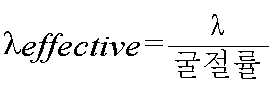
상기 식에서, λ는 유체 메니스커스로 들어가기 전의 패터닝된 광의 파장이며, λeffective 는 웨이퍼 표면 상의 포토레지스트에 도포된 패터닝된 광의 유효 파장이다. 일 실시형태에서, 물은 액침 리소그래피용 유체로서 이용될 수도 있다. 물은 1.43의 굴절률을 가지며, 따라서 리소그래피 렌즈가 유체 메니스커스에 193 ㎚의 파장을 이용한다면, 포토레지스트에 이용된 광학 신호의 유효 파장은 약 135 ㎚로 축소될 수도 있다. 따라서, 리소그래피 렌즈가 유체 메니스커스의 액체에 직접 접촉하는 구성을 이용함으로써, 리소그래피 렌즈로부터의 광의 유효 파장은 상당히 감소될 수도 있다. 웨이퍼 표면 상의 포토레지스트를 충격하는 감소된 유효 파장의 광은 포토레지스트를 소망하는 임의의 적절한 패턴으로 패터닝할 수도 있다. 광원으로부터의 광은 소망하는 패턴을 발생시킬 수도 있는 레티클을 통해 전송될 수도 있다. 광원은 예를 들어 자외선 램프, 엑시머 레이저 등과 같은 포토레지스트를 패터닝할 수 있는 광학 신호를 발생시킬 수도 있는 임의의 적절한 장치일 수도 있다. 레티클은 당업자에게 공지된 임의의 적절한 방법을 이용하여 제조할 수 있다.Where λ is the wavelength of the patterned light before entering the fluid meniscus and λ effective is the effective wavelength of the patterned light applied to the photoresist on the wafer surface. In one embodiment, water may be used as a fluid for immersion lithography. Water has a refractive index of 1.43, so if the lithographic lens uses a wavelength of 193 nm for the fluid meniscus, the effective wavelength of the optical signal used in the photoresist may be reduced to about 135 nm. Thus, by using a configuration in which the lithographic lens is in direct contact with the liquid of the fluid meniscus, the effective wavelength of light from the lithographic lens may be significantly reduced. The reduced effective wavelength of light impacting the photoresist on the wafer surface may pattern the photoresist in any suitable pattern as desired. Light from the light source may be transmitted through a reticle that may generate a desired pattern. The light source may be any suitable device that may generate an optical signal capable of patterning a photoresist such as, for example, an ultraviolet lamp, an excimer laser, or the like. The reticle can be prepared using any suitable method known to those skilled in the art.
일 실시형태에서, 리소그래피 렌즈 구조 (200) 는, 예를 들어, 도 2에 도시한 컬럼 시스템 (202) 과 같은 패터닝된 광 발생 장치에 장착된다. 컬럼 시스템 (202) 은 광원과, 광원으로부터의 패터닝되지 않은 광이 레티클을 통해 투과하여 포토레지스트 (110) 의 패터닝을 위한 리소그래피 렌즈 구조 (200) 를 통해 투 과하는 패터닝된 광을 발생시키는 레티클을 갖는 임의의 적절한 장치일 수도 있다. 리소그래피 렌즈 구조 (200) 는 컬럼 시스템 (202) 으로부터 유체 메니스커스 (112) 로 패터닝된 광 신호의 전달을 용이하게 할 수 있는 근접 헤드 내에 적어도 부분적으로 정의될 수 있는 임의의 적절한 구성 및/또는 사이즈의 임의의 적절한 구조일 수도 있다는 것을 이해할 것이다. 일 실시형태에서, 패터닝된 광은 컬럼 시스템 (202) 으로부터 리소그래피 렌즈 구조 (200) 의 렌즈를 통해 유체 메니스커스 (112) 로 직접 투과될 수 있다. 이로 부터, 패터닝된 광은 유체 메니스커스 (112) 를 통해 웨이퍼 (108) 의 표면 상의 포토레지스트 (110) 로 이동할 수 있다. 패터닝된 광은 그 후 포토레지스트에 이용되어 포토레지스트 (110) 상에 패턴이 제공된다. 그러므로, 일 실시형태에서, 리소그래피 렌즈 구조 (200) 는 리소그래피 렌즈 구조 (200) 를 통해 연장되는 통로 내에 하나 이상의 렌즈를 포함할 수 있으며, 따라서 근접 헤드 (106) 의 상부로부터 근접 헤드 (106) 의 바닥부분으로의 광 투과가 발생한다. 패터닝된 광은 임의의 적절한 방법으로 발생될 수도 있으며 본 명세서에 기술된 실시형태는 당연히 단지 예시일 뿐임을 이해할 것이다.In one embodiment,
유체 메니스커스는 웨이퍼 표면 상의 포토레지스트에 패터닝 광을 이용하는 동시에 웨이퍼 표면에 유체를 도포하고 표면으로부터 유체를 제거함으로써 웨이퍼를 프로세스하기 위해 웨이퍼를 가로질러 이동될 수도 있다. 일 실시형태에서, 스텝퍼 장치는 리소그래피 렌즈를 패터닝될 웨이퍼 부분 상부에 이동시키는데 사용될 수도 있다. 웨이퍼 (108) 는 포토리소그래피 패터닝 작업이 진행됨에 따라 래스터화된 운동으로 이동될 수도 있다. 시스템 (100) 은 웨이퍼의 일 표면 또는 웨이퍼의 상부 표면 및 하부 표면의 양쪽 표면 모두를 프로세스할 수 있다.The fluid meniscus may be moved across the wafer to process the wafer by using patterning light in the photoresist on the wafer surface while simultaneously applying fluid to and removing fluid from the surface of the wafer. In one embodiment, the stepper apparatus may be used to move the lithographic lens over the portion of the wafer to be patterned.
일 실시형태에서, 유체 메니스커스 (112) 는 유체를 웨이퍼 표면에 도포하고 본 명세서에 기술된 근접 헤드에 위치된 소스 입구 및 소스 출구와 같은 도관을 통해 웨이퍼 표면으로부터 유체를 제거함으로써 발생된다. 예를 들어, 입구 및 출구와 같은 도관은 근접 헤드의 정면 상에 위치된 개구부를 가지며, 여기서 기술한 안정한 메니스커스가 이용될 수 있는 한 임의의 적절한 형상일 수도 있다.In one embodiment, the
일 예시적인 실시형태에서, 하나 이상의 가스 입구는 하나 이상의 프로세스 유체 입구에 교대로 인접하여 가스 진공 프로세스 유체 배향을 형성할 수도 있는 하나 이상의 진공 출구에 인접할 수도 있다. 소망하는 웨이퍼 프로세스 및 어떤 형태의 웨이퍼 프로세스 메커니즘이 강화되는 것을 원하는 지에 따라서, 가스-프로세스 유체-진공, 프로세스 유체-진공-가스, 진공-가스-프로세스 유체 등과 같은 다른 형태의 배향이 사용될 수도 있다는 것을 이해할 것이다. 다른 실시형태에서, 근접 헤드와 웨이퍼 사이에 웨이퍼를 프로세스 하기 위해 위치된 메니스커스를 종합적이고 강하게 발생시키고, 제어하고 이동시키기 위해 가스-진공-프로세스 유체 배향이 이용될 수도 있다. 유체 메니스커스를 관리하는 능력을 가짐으로써, 리소그래피 렌즈는 한 위치에 고정될 수도 있고, 따라서 액체/렌즈 계면 및 액체/포토레지스트 계면은 포토레지스트에 이용되는 광학 신호의 유효 파장을 감소시킬 수 있다.In one exemplary embodiment, the one or more gas inlets may be adjacent to one or more vacuum outlets that may alternately adjacent one or more process fluid inlets to form a gas vacuum process fluid orientation. Depending on the desired wafer process and what type of wafer process mechanism is desired to be strengthened, other forms of orientation may be used, such as gas-process fluid-vacuum, process fluid-vacuum-gas, vacuum-gas-process fluid, and the like. Will understand. In other embodiments, gas-vacuum-process fluid orientation may be used to comprehensively and strongly generate, control and move the meniscus positioned to process the wafer between the proximity head and the wafer. By having the ability to manage the fluid meniscus, the lithographic lens may be fixed in one position, thus the liquid / lens interface and liquid / photoresist interface may reduce the effective wavelength of the optical signal used in the photoresist. .
프로세스 유체 입구, 가스 입구 및 진공 출구는 유체 메니스커스가 안정적인 방식으로 발생되고 유지될 수도 있는 경우, 임의의 적절한 방식으로 배열될 수도 있다. 예를 들어, 가스 입구, 진공 출구, 및 프로세스 유체 입구에 부가하여, 추가적인 실시형태에서, 바람직한 근접 헤드의 구성에 따라 가스 입구, 프로세스 유체 입구 및/또는 진공 출구의 추가적인 세트가 있을 수도 있다. 가스-진공-프로세스 유체 배향의 정확한 구성은 애플리케이션에 따라 달라질 수도 있다. 예를 들어, 가스 입구, 진공 및 프로세스 유체 입구 위치 사이의 거리는 변화될 수도 있으며, 따라서 그 거리는 일정하거나 또는 그 거리는 비일정하다. 또한, 가스 입구, 진공 및 프로세스 유체 입구 사이의 거리는 근접 헤드 (106) 의 사이즈, 형상 및 구성과, 프로세스 메니스커스의 소망하는 사이즈 (즉, 메니스커스 형상 및 사이즈) 에 따라 크게 상이할 수도 있다.The process fluid inlet, gas inlet and vacuum outlet may be arranged in any suitable manner if the fluid meniscus may be generated and maintained in a stable manner. For example, in addition to the gas inlet, vacuum outlet, and process fluid inlet, in further embodiments, there may be an additional set of gas inlet, process fluid inlet, and / or vacuum outlet, depending on the configuration of the preferred proximity head. The exact configuration of the gas-vacuum-process fluid orientation may vary depending on the application. For example, the distance between the gas inlet, vacuum and process fluid inlet locations may vary, so the distance is constant or the distance is non-uniform. Further, the distance between the gas inlet, the vacuum and the process fluid inlet may vary greatly depending on the size, shape and configuration of the
일 실시형태에서, 근접 헤드 (106) 는 웨이퍼 (108) 의 상부 표면에 아주 근접하게 위치할 수도 있으며 가스, 프로세스 유체 및 진공 출구를 이용하여 상부 표면을 프로세스할 수 있는 웨이퍼 (108) 와 접촉된 웨이퍼 프로세스 메니스커스를 발생한다. 일 실시형태에서, IPA/N2 증기 가스는 가스 입구를 통해 가스로 투입되고 탈이온수는 프로세스 유체 입구를 통해 프로세스 유체로 투입될 수도 있다. IPA 및 프로세스 유체가 투입되는 것과 거의 동시에 진공이 웨이퍼의 아주 근접한 위치에 적용되어 IPA 증기, 프로세스 유체, 및/또는 웨이퍼 표면상에 존재할 수도 있는 유체를 제거한다. IPA가 예시적인 실시형태에서 이용되지만, 임의의 다른 적절한 타입의 증기, 예를 들어, 그 증기가 비활성 가스를 통해 이동될 수 있는 유 체 메니스커스를 발생하는데 이용되는 액체와 섞일 수 있는 알콜 (에탄올, 프로판올, 부탄올, 헥산올 등), 케톤, 에테르, 또는 다른 유기 화합물 등의 임의의 적절한 증기가 이용될 수도 있다. 근접 헤드와 웨이퍼 사이의 영역에 존재하는 프로세스 유체의 일부는 메니스커스이다. 여기 사용된 대로, "산출"이라는 용어는 웨이퍼 (108) 와 특정 근접 헤드 사이의 영역으로부터 유체를 제거하는 것을 지칭할 수 있으며, "투입"이라는 용어는 웨이퍼 (108) 와 특정 근접 헤드 사이의 영역으로의 유체의 유입일 수 있다.In one embodiment, the
일 실시형태에서, 시스템 (100) 은 근접 헤드 (106) 로 유체를 공급하고, 근접헤드 (106) 로부터 유체를 제거할 수 있는 유체 공급 분배기를 더 구비한다. 유체 공급 분배기는, 예를 들어, 매니폴드와 같은 제어된 방식으로 유체를 공급하고 수용할 수 있는 임의의 적절한 장치일 수도 있다. 일 실시형태에서, 유체 공급 분배기는 유체 공급부로부터 유체를 공급받는다. 유체 공급부는 근접 헤드 (106) 로의 유체 투입을 관리할 수 있는 임의의 적절한 하드웨어/소프트웨어일 수도 있는 유체 공급 제어에 의해 관리되고 제어될 수도 있다. 근접 헤드 (106) 는 그 후 웨이퍼 (108) 를 프로세스할 수 있는 메니스커스를 생성할 수도 있다.In one embodiment, the
도 3a는 본 발명의 일 실시형태에 따른 리소그래피 렌즈 구조 (200) 를 갖는 근접 헤드 (106) 를 도시한다. 상기에서 논의한 바와 같이, 리소그래피 렌즈 (200) 는 웨이퍼 표면 상의 포토레지스트를 패터닝할 수 있는 패터닝된 광을 발생시킬 수 있는 임의의 적절한 장치에 접속될 수도 있다. 일 실시형태에서, 도 2 에 도시한 바와 같이, 패터닝된 광 발생 장치는 리소그래피 렌즈 구조 (200) 의 상부에 장착될 수 있는 컬럼 시스템 (202) 이다. 리소그래피 렌즈 구조 (200) 는 유체 메니스커스와 직접 접촉할 수 있는 렌즈를 포함하며 패터닝된 광을 유체 메니스커스를 통해 포토레지스트로 투과시킨다. 일 실시형태에서, 렌즈는 예를 들어, CaF2, 석영 등과 같은 바람직한 파장의 광을 투과시킬 수 있는 임의의 적절한 재료로 제조될 수도 있다.3A shows a
일 실시형태에서, 근접 헤드 (106) 는 출구 (304) 뿐만 아니라 입구 (302 및 306) 를 구비한다. 액침 리소그래피 작업의 일 예시적인 실시형태에서, (도 3b 및 도 3c를 참조하여 더 상세하게 논의한 바와 같이) 근접 헤드 (106) 는 유체 메니스커스를 제조할 수도 있으며, 상기 유체 메니스커스를 통해 리소그래피 렌즈 구조 (200) 는 패터닝 광을 통과시켜 웨이퍼 (108) 표면 상의 포토레지스트를 패터닝할 수 있다. 입구 (302 및 306) 는 소망하는 구체적인 웨이퍼 프로세스 작업에 따라 임의의 적절한 표면 장력 감소 가스/증기 및 프로세스 유체를 각각 투입할 수도 있다. 출구 (304) 는 웨이퍼 (108) 의 표면으로부터 (웨이퍼 (108) 상의 임의의 다른 유체뿐만 아니라) 표면 장력 감소 가스 및 프로세스 유체의 임의의 적절한 양을 제거할 수 있는 진공을 발생시킨다. 그 결과, 근접 헤드 (106) 는 본 명세서에 기술된 유체 메니스커스의 발생을 가능하게 하여 패터닝 광이 투과될 수도 있는 유체 매체를 발생시킬 수도 있다. 그러한 예시적인 실시형태에서, 근접 헤드 (106) 는 웨이퍼 (108) 를 프로세스할 수도 있으며, 따라서 컬럼 구조의 레티클 내부에 의해 정의된 패턴은 패터닝된 광을 리소그래피 렌즈 구조 (200) 의 렌즈를 통해 통과시킴으로써 포토레지스트에 투과시킬 수도 있다. 렌즈는 유체 메니스커스와 직접 접촉될 수도 있으며, 따라서 렌즈로부터의 패터닝된 광은 유체 메니스커스로 들어가고 유체메니스커스를 통해 근접 헤드 (106) 에 의해 발생된 유체 메니스커스와 직접 접촉할 수도 있는 포토레지스트로 투과될 수도 있다. 패터닝된 광이 리소그래피 렌즈로부터 유체 메니스커스로 이동할 때, 유체 메니스커스의 굴절률은 포토레지스트에 이용되는 패터닝된 광의 유효 파장을 감소시킬 수도 있다.In one embodiment, the
근접 헤드 (106) 의 다른 실시형태에서, 입구 (302) 는 제거되고 입구 (306) 와 출구 (304) 만이 남을 수도 있다. 그러한 구성에서, 출구 (304) 및 입구 (306) 가 위치된 영역은 근접 헤드 (106) 의 프로세스 표면의 나머지에 비해 거칠 수도 있다. 따라서, 유체 메니스커스는 감금 가스 및/또는 표면 장력 변경 가스를 공급할 필요가 없는 거친 영역 내에 함유될 수도 있다. 따라서, 프로세스 유체는 입구 (306) 를 통해 투입될 수도 있으며 프로세스 유체는 출구 (304) 를 통해 제거되어 포토리소그래피가 발생할 수 있는 안정한 메니스커스를 발생시킨다.In another embodiment of the
도 3b는 본 발명의 일 실시형태에 따른 근접 헤드 (106) 의 내부 구조의 측면도를 도시한다. 일 실시형태에서, 근접 헤드 (106) 는 소스 출구 (304) 뿐만 아니라 소스 입구 (302 및 306) 를 구비한다. 일 실시형태에서, 예를 들어, 탈이온수 (DIW) 와 같은 프로세스 유체가 소스 입구 (306) 를 통해 웨이퍼 표면에 대해 이용되므로, 유체는 예를 들어, 소스 입구 (302) 를 통해 IPA/N2 와 같은 가스의 이용에 의해 감금될 수도 있는 유체 메니스커스 및 IPA/N2 와 DIW를 제거할 수 있는 진공 (304) 을 형성한다. 유체 메니스커스는 리소그래피 렌즈 구조 (200) 의 렌즈와 웨이퍼 표면 상의 포토레지스트 모두와 접촉하여 리소그래피 렌즈 구조 (200) 로부터의 패터닝 광이 포토레지스트에 이용될 수도 있는 매체를 제공한다. 일 실시형태에서, 리소그래피 렌즈 구조 (200) 는 컬럼 시스템으로부터의 패터닝된 광을 유체 메니스커스에 직접 투과시킬 수 있는 렌즈 (200a) 를 구비한다. 상기에 논의한 바와 같이, 소스 입구 (302) 는 유체 메니스커스를 구성하는 액체의 표면 장력을 감소시킬 수 있는 임의의 적절한 타입의 가스를 투입할 수도 있다. 일 실시형태에서, 가스는 유체 메니스커스의 액체/기체 경계에서 표면 장력 구배를 발생시킨다. 일 실시형태에서, 가스는 알콜의 그룹, 케톤 또는 유체 메니스커스를 발생시키는데 이용되는 액체와 섞일 수도 있는 표면장력에 영향을 주는 성질을 갖는 다른 유기 화합물로부터의 표면 장력에 영향을 주는 유체의 적절한 증기이다. 바람직한 실시형태에서, 가스는 질소 가스 내의 이소프로필 알콜 증기 (IPA/N2) 이다. 그러한 실시형태에서, IPA/N2 는, 예를 들어, 물과 같은 액체의 표면 장력을 감소시킬 수 있다. 그러므로, 일 실시형태에서, 유체 메니스커스 내의 DIW는 계속 보충되기 때문에, 물 표면은 리소그래피 작업 동안에 거의 깨끗한 상태로 유지될 수도 있다. 또한, 유체 메니스커스를 형성하고 유지하는 하드웨어가 구성될 수도 있으며, 따라서 유체 메니스커스 내의 버블링은 최소로 유지되거나 완전히 제거될 수도 있으며, 그에 의해 패터닝 작업을 최적화한다. 그러한 방식으로, 웨이퍼 표면상에 오염을 남기지 않는 안정한 메니스커스가 발생될 수도 있으며, 그 이유는 물/가스가 웨이퍼 표면상에 오염을 남길 수 있는 물 비딩 효과 (water beading effect) 를 제거하기 때문이고, 따라서 프로세스 후에 건조하고 깨끗한 표면을 남긴다.3B shows a side view of the internal structure of the
다른 실시형태에서, 유체 메니스커스는 엄격하게 제어된 온도에서 유지되어 유효 파장을 제어할 수도 있으며, 또한, 온도를 낮추어 유체의 굴절률을 증가시킬 수 있으며, 따라서 유효 파장을 감소시킨다.In another embodiment, the fluid meniscus may be maintained at a strictly controlled temperature to control the effective wavelength, and may also lower the temperature to increase the refractive index of the fluid, thus reducing the effective wavelength.
도 3c는 본 발명의 일 실시형태에 따른 작업의 근접 헤드 (106) 를 도시한다. 이 실시형태에서, 근접 헤드 (106) 는 작업중이고 액체/기체 계면 (388) 을 갖는 유체 메니스커스 (112) 를 발생시켰다. 일 실시형태에서, 예를 들어, 탈이온수 (DIW) 와 같은 리소그래피 렌즈 구조 (200) 로부터의 광의 유효 파장을 감소시킬 수 있는 굴절률을 갖는 액체가 방향 화살표 (314) 로 도시된 바와 같이 투입된다. 또한, 예를 들어, IPA/N2 와 같은 표면장력에 영향을 줄 수 있는 가스와 같은 가스 증기가 방향 화살표 (310) 로 도시된 바와 같이 투입될 수도 있다. DIW 및 IPA/N2 는 방향 화살표 (312) 에 의해 도시된 바와 같이 웨이퍼 표면 상의 포토레지스트로부터 제거될 수도 있다. 일 실시형태에서, 진공을 이용함으로써 DIW 및 IPA/N2 제거한다. 이 방법에 의해, 유체 메니스커스 (112) 는 리소그래피 렌즈 구조 (200) 가 패터닝된 광 (400) 을 이용할 수도 있는 웨이퍼 표면상에 발생될 수도 있다. 리소그래피 렌즈 구조 (200) 의 렌즈 (200a) 가 유체 메니 스커스 (112) 에 접촉하고 유체 메니스커스 (112) 가 포토레지스트에 접촉하므로, 유체 메니스커스 (112) 를 구성하는 액체의 굴절률은 리소그래피 렌즈 구조 (200) 로부터 포토레지스트 (110) 로 인가되는 패터닝된 광 (400) 의 유효 파장을 감소시킬 수도 있다. 그러한 실시형태에서, 리소그래피 렌즈 구조 (200) 의 렌즈 (200a) 는 유체 메니스커스 (112) 를 갖는 렌즈/액체 계면 (402) 을 형성하고, 유체 메니스커스 (112) 는 차례로 포토레지스트 (110) 와 함께 액체-포토레지스트 계면 (404) 을 형성한다. 이어서, 패터닝된 광 (400) 은 리소그래피 렌즈 구조 (200) 로부터 메니스커스를 통해 포토레지스트로 투과되어 웨이퍼 (108) 상의 포토레지스트 (110) 에 영역 (390) 을 패터닝한다.3C shows a
도 4a는 본 발명의 일 실시형태에 따라 다른 방법의 예시적인 입구/출구 구성을 갖는 근접 헤드 (106') 를 도시한다. 일 실시형태에서, 근접 헤드 (106') 는 근접 헤드 (106') 의 일측 상에 소스 입구 (306) 를 갖는 리소그래피 렌즈 구조 (200) 를 포함한다. 근접 헤드 (106') 는 또한 리소그래피 렌즈 구조 (200) 의 타측 상에 소스 출구 (304) 를 구비한다. 일 실시형태에서, 소스 입구 (302) 는 리소그래피 렌즈 구조 (200), 소스 입구 (302), 및 소스 출구 (304) 를 실절적으로 둘러쌀 수도 있다.4A shows a proximity head 106 'having an exemplary inlet / outlet configuration of another method in accordance with one embodiment of the present invention. In one embodiment, the proximity head 106 'includes a
도 4b는 본 발명의 일 실시형태에 따른 다른 방법의 예시적인 입구/출구 구성을 갖는 근접 헤드 (106) 의 내부 구조의 측면을 도시한다. 일 실시형태에서, 근접 헤드 (106) 는 리소그래피 렌즈 구조 (200) 의 상부에 장착될 수 있는 컬럼 시스템에 의해 발생된 패터닝된 광을 투과시킬 수 있는 렌즈 (200a) 를 구비하 는 리소그래피 렌즈 구조 (200) 를 포함한다. 패터닝된 광은 프로세스될 웨이퍼 표면 상의 포토레지스트 상에 발생된 바람직한 패턴에 상응한다. 근접 헤드 (106) 는 리소그래피 렌즈 구조 (200) 의 일측에 소스 입구 (302 및 306) 를 구비하고 리소그래피 렌즈 구조 (200) 의 타측에 소스 입구 (302) 및 소스 출구 (304) 를 구비할 수도 있다. 그러한 구성에서, 소스 입구 (306) 를 통해 투입된 액체는 웨이퍼 표면 상의 포토레지스트에 도포될 수도 있다. 소스 입구 (302) 는 가스를 소스 입구 (306) 로부터의 액체에 효과적으로 가하여 소스 입구 (302) 로부터의 액체가 함유될 수도 있도록 가스를 웨이퍼 표면에 가할 수도 있다. 소스 출구 (304) 는 소스 출구 (304) 와 같은 쪽의 소스 입구 (302) 로부터의 가스의 일부뿐만 아니라 소스 입구 (302) 로부터의 액체도 제거할 수도 있다. 따라서 이 실시형태는 또한 하기에 기술한 리소그래피 작업을 용이하게 하는 안정한 유체 메니스커스를 발생시킨다.4B shows a side view of an internal structure of a
도 4c는 본 발명의 일 실시형태에 따른 리소그래피 작업을 수행하는 근접 헤드 (106') 를 도시한다. 일 실시형태에서, 근접 헤드 (106') 는 액체/기체 계면 (388) 을 갖는 유체 메니스커스 (112) 를 발생시켰다. 일 실시형태에서, 예를 들어, 탈이온수 (DIW) 와 같은 리소그래피 렌즈 구조 (200) 로부터의 광의 유효 파장을 감소시킬 수 있는 굴절률을 갖는 액체가 방향 화살표 (314) 로 도시한 바와 같이 투입된다. 또한, 예를 들어, IPA/N2 와 같은 표면 장력 감소 가스가 방향 화살표 (310) 로 도시한 바와 같이 투입될 수도 있다. DIW 및 IPA/N2 는 방향 화살표 (312) 로 도시한 바와 같이 웨이퍼 표면 상의 포토레지스트로부터 제거될 수도 있다. 이 방법에 의해, 다이나믹 유체 메니스커스가 웨이퍼 표면상에 발생될 수도 있으며, 웨이퍼 표면을 통해 리소그래피 렌즈 구조 (200) 는 패터닝된 광 (400) 을 이용할 수 있다. 패터닝된 광 (400) 은 리소그래피 렌즈 구조 (200) 로부터 유체 메니스커스를 통해 포토레지스트로 이동할 수도 있다. 리소그래피 렌즈 구조 (200) 는 유체 메니스커스 (112) 에 접촉하므로, 유체 메니스커스 (112) 를 구성하는 액체의 굴절률은 리소그래피 렌즈 구조 (200) 로부터의 패터닝된 광 (400) 의 유효 파장을 감소시킬 수도 있다. 유효 파장이 감소된 패터닝된 광 (400) 은 웨이퍼 표면상에 포토레지스트의 영역 (390) 을 패터닝할 수도 있다. 그러한 실시형태에서, 리소그래피 렌즈 구조 (200) 의 렌즈 (200a) 는 유체 메니스커스 (112) 와 렌즈-액체 계면 (402) 를 형성할 수도 있으며, 유체 메니스커스 (112) 는 포토레지스트 (110) 와 액체-포토레지스트 계면 (404) 을 차례로 형성할 수도 있다. 이어서, 패터닝된 광 (400) 은 리소그래피 렌즈 구조 (200) 로부터 메니스커스를 통해 포토레지스트로 이동하여 웨이퍼 (108) 상의 포토레지스트의 영역 (390) 을 패터닝할 수 있다.4C shows a proximity head 106 'performing a lithographic operation according to one embodiment of the present invention. In one embodiment, the
본 발명을 몇몇 바람직한 실시형태에 관해 설명하였지만, 당업자가 상술한 명세서를 읽고 도면을 연구하여 다양한 변경, 부가, 치환 및 그 동등물을 구현할 수 있음이 이해될 것이다. 따라서, 본 발명은 본 발명의 진정한 정신 및 범위 내의 그러한 모든 변경, 부가, 치환 및 동등물을 포함하는 것을 의도한다.While the present invention has been described in terms of some preferred embodiments, it will be understood by those skilled in the art that various modifications, additions, substitutions, and equivalents thereof may be made by reading the above specification and studying the drawings. Accordingly, the present invention is intended to embrace all such alterations, additions, substitutions, and equivalents within the true spirit and scope of the present invention.
Claims (31)
Applications Claiming Priority (5)
| Application Number | Priority Date | Filing Date | Title |
|---|---|---|---|
| US10/606,022 | 2003-06-24 | ||
| US10/606,022 US7252097B2 (en) | 2002-09-30 | 2003-06-24 | System and method for integrating in-situ metrology within a wafer process |
| US10/834,548 | 2004-04-28 | ||
| US10/834,548 US7367345B1 (en) | 2002-09-30 | 2004-04-28 | Apparatus and method for providing a confined liquid for immersion lithography |
| PCT/US2004/020332 WO2005003864A2 (en) | 2003-06-24 | 2004-06-23 | Apparatus and method for providing a confined liquid for immersion lithography |
Publications (2)
| Publication Number | Publication Date |
|---|---|
| KR20060025189A true KR20060025189A (en) | 2006-03-20 |
| KR101117052B1 KR101117052B1 (en) | 2012-02-22 |
Family
ID=33568007
Family Applications (1)
| Application Number | Title | Priority Date | Filing Date |
|---|---|---|---|
| KR1020057024769A Expired - Fee Related KR101117052B1 (en) | 2003-06-24 | 2004-06-23 | Apparatus and method for providing a confined liquid for immersion lithography |
Country Status (9)
| Country | Link |
|---|---|
| US (2) | US7367345B1 (en) |
| EP (1) | EP1636654B1 (en) |
| JP (1) | JP4612630B2 (en) |
| KR (1) | KR101117052B1 (en) |
| AT (1) | ATE465435T1 (en) |
| DE (1) | DE602004026725D1 (en) |
| MY (1) | MY139592A (en) |
| TW (1) | TWI289734B (en) |
| WO (1) | WO2005003864A2 (en) |
Cited By (3)
| Publication number | Priority date | Publication date | Assignee | Title |
|---|---|---|---|---|
| KR101283945B1 (en) * | 2010-10-18 | 2013-07-11 | 에이에스엠엘 네델란즈 비.브이. | A fluid handling structure, a lithographic apparatus and a device manufacturing method |
| KR101341927B1 (en) * | 2010-08-23 | 2014-01-02 | 에이에스엠엘 네델란즈 비.브이. | Fluid Handling Structure, Module for an Immersion Lithographic Apparatus, Lithographic Apparatus and Device Manufacturing Method |
| US8988650B2 (en) | 2010-08-24 | 2015-03-24 | Asml Netherlands B.V. | Lithographic apparatus and device manufacturing method |
Families Citing this family (118)
| Publication number | Priority date | Publication date | Assignee | Title |
|---|---|---|---|---|
| US20040031167A1 (en) | 2002-06-13 | 2004-02-19 | Stein Nathan D. | Single wafer method and apparatus for drying semiconductor substrates using an inert gas air-knife |
| US7520285B2 (en) * | 2002-09-30 | 2009-04-21 | Lam Research Corporation | Apparatus and method for processing a substrate |
| US7198055B2 (en) * | 2002-09-30 | 2007-04-03 | Lam Research Corporation | Meniscus, vacuum, IPA vapor, drying manifold |
| US7372541B2 (en) | 2002-11-12 | 2008-05-13 | Asml Netherlands B.V. | Lithographic apparatus and device manufacturing method |
| US9482966B2 (en) | 2002-11-12 | 2016-11-01 | Asml Netherlands B.V. | Lithographic apparatus and device manufacturing method |
| CN100470367C (en) | 2002-11-12 | 2009-03-18 | Asml荷兰有限公司 | Photolithography apparatus and device manufacturing method |
| TWI251127B (en) | 2002-11-12 | 2006-03-11 | Asml Netherlands Bv | Lithographic apparatus and device manufacturing method |
| US10503084B2 (en) | 2002-11-12 | 2019-12-10 | Asml Netherlands B.V. | Lithographic apparatus and device manufacturing method |
| CN101872135B (en) | 2002-12-10 | 2013-07-31 | 株式会社尼康 | Exposure system and device producing method |
| AU2003289271A1 (en) | 2002-12-10 | 2004-06-30 | Nikon Corporation | Exposure apparatus, exposure method and method for manufacturing device |
| SG158745A1 (en) | 2002-12-10 | 2010-02-26 | Nikon Corp | Exposure apparatus and method for producing device |
| JP4352874B2 (en) | 2002-12-10 | 2009-10-28 | 株式会社ニコン | Exposure apparatus and device manufacturing method |
| US7242455B2 (en) | 2002-12-10 | 2007-07-10 | Nikon Corporation | Exposure apparatus and method for producing device |
| KR101037057B1 (en) | 2002-12-10 | 2011-05-26 | 가부시키가이샤 니콘 | Exposure apparatus and device manufacturing method |
| US7948604B2 (en) | 2002-12-10 | 2011-05-24 | Nikon Corporation | Exposure apparatus and method for producing device |
| DE10261775A1 (en) | 2002-12-20 | 2004-07-01 | Carl Zeiss Smt Ag | Device for the optical measurement of an imaging system |
| TWI621923B (en) | 2003-02-26 | 2018-04-21 | 尼康股份有限公司 | Exposure apparatus, exposure method, and component manufacturing method |
| EP1610361B1 (en) | 2003-03-25 | 2014-05-21 | Nikon Corporation | Exposure system and device production method |
| WO2004090956A1 (en) * | 2003-04-07 | 2004-10-21 | Nikon Corporation | Exposure apparatus and method for manufacturing device |
| KR20110104084A (en) | 2003-04-09 | 2011-09-21 | 가부시키가이샤 니콘 | Immersion Lithography Fluid Control System |
| EP1611486B1 (en) | 2003-04-10 | 2016-03-16 | Nikon Corporation | Environmental system including a transport region for an immersion lithography apparatus |
| EP3352010A1 (en) | 2003-04-10 | 2018-07-25 | Nikon Corporation | Run-off path to collect liquid for an immersion lithography apparatus |
| EP2950148B1 (en) | 2003-04-10 | 2016-09-21 | Nikon Corporation | Environmental system including vaccum scavenge for an immersion lithography apparatus |
| CN101980087B (en) | 2003-04-11 | 2013-03-27 | 株式会社尼康 | Immersion exposure appratus and method |
| SG10201803122UA (en) | 2003-04-11 | 2018-06-28 | Nikon Corp | Immersion lithography apparatus and device manufacturing method |
| JP4582089B2 (en) | 2003-04-11 | 2010-11-17 | 株式会社ニコン | Liquid jet recovery system for immersion lithography |
| JP2006523958A (en) | 2003-04-17 | 2006-10-19 | 株式会社ニコン | Optical structure of an autofocus element for use in immersion lithography |
| TWI295414B (en) | 2003-05-13 | 2008-04-01 | Asml Netherlands Bv | Lithographic apparatus and device manufacturing method |
| CN100437358C (en) | 2003-05-15 | 2008-11-26 | 株式会社尼康 | Exposure apparatus and device manufacturing method |
| TWI612557B (en) | 2003-05-23 | 2018-01-21 | Nikon Corporation | Exposure method and exposure apparatus and component manufacturing method |
| TWI612556B (en) | 2003-05-23 | 2018-01-21 | 尼康股份有限公司 | Exposure apparatus, exposure method, and component manufacturing method |
| KR101548832B1 (en) | 2003-05-28 | 2015-09-01 | 가부시키가이샤 니콘 | Exposure method, exposure device, and device manufacturing method |
| US7213963B2 (en) | 2003-06-09 | 2007-05-08 | Asml Netherlands B.V. | Lithographic apparatus and device manufacturing method |
| US7317504B2 (en) | 2004-04-08 | 2008-01-08 | Asml Netherlands B.V. | Lithographic apparatus and device manufacturing method |
| EP1486827B1 (en) | 2003-06-11 | 2011-11-02 | ASML Netherlands B.V. | Lithographic apparatus and device manufacturing method |
| EP3104396B1 (en) | 2003-06-13 | 2018-03-21 | Nikon Corporation | Exposure method, substrate stage, exposure apparatus, and device manufacturing method |
| TWI564933B (en) | 2003-06-19 | 2017-01-01 | 尼康股份有限公司 | An exposure apparatus, an exposure method, and an element manufacturing method |
| US6809794B1 (en) * | 2003-06-27 | 2004-10-26 | Asml Holding N.V. | Immersion photolithography system and method using inverted wafer-projection optics interface |
| US7236232B2 (en) | 2003-07-01 | 2007-06-26 | Nikon Corporation | Using isotopically specified fluids as optical elements |
| EP1652003B1 (en) | 2003-07-08 | 2015-01-07 | Nikon Corporation | Wafer table for immersion lithography |
| JP4515385B2 (en) | 2003-07-09 | 2010-07-28 | 株式会社ニコン | Exposure apparatus, exposure method, and device manufacturing method |
| WO2005006418A1 (en) | 2003-07-09 | 2005-01-20 | Nikon Corporation | Exposure apparatus and method for manufacturing device |
| JP4844123B2 (en) | 2003-07-09 | 2011-12-28 | 株式会社ニコン | Exposure apparatus and device manufacturing method |
| EP1650787A4 (en) | 2003-07-25 | 2007-09-19 | Nikon Corp | Inspection method and inspection device for projection optical system, and production method for projection optical system |
| EP1503244A1 (en) | 2003-07-28 | 2005-02-02 | ASML Netherlands B.V. | Lithographic projection apparatus and device manufacturing method |
| CN104122760B (en) | 2003-07-28 | 2017-04-19 | 株式会社尼康 | Exposure apparatus and device manufacturing method |
| US7175968B2 (en) | 2003-07-28 | 2007-02-13 | Asml Netherlands B.V. | Lithographic apparatus, device manufacturing method and a substrate |
| US7326522B2 (en) | 2004-02-11 | 2008-02-05 | Asml Netherlands B.V. | Device manufacturing method and a substrate |
| US7779781B2 (en) | 2003-07-31 | 2010-08-24 | Asml Netherlands B.V. | Lithographic apparatus and device manufacturing method |
| KR101419192B1 (en) | 2003-08-29 | 2014-07-15 | 가부시키가이샤 니콘 | Exposure apparatus and device producing method |
| EP1659620A4 (en) | 2003-08-29 | 2008-01-30 | Nikon Corp | LIQUID RECOVERY DEVICE, EXPOSURE DEVICE, EXPOSURE METHOD, AND CORRESPONDING PRODUCTION DEVICE |
| TWI263859B (en) | 2003-08-29 | 2006-10-11 | Asml Netherlands Bv | Lithographic apparatus and device manufacturing method |
| KR101238114B1 (en) | 2003-09-03 | 2013-02-27 | 가부시키가이샤 니콘 | Apparatus and method for providing fluid for immersion lithography |
| JP4444920B2 (en) | 2003-09-19 | 2010-03-31 | 株式会社ニコン | Exposure apparatus and device manufacturing method |
| KR101441840B1 (en) | 2003-09-29 | 2014-11-04 | 가부시키가이샤 니콘 | Exposure apparatus, exposure method, and device manufacturing method |
| EP1672682A4 (en) | 2003-10-08 | 2008-10-15 | Zao Nikon Co Ltd | APPARATUS AND METHOD FOR TRANSPORTING SUBSTRATE, APPARATUS AND METHOD FOR EXPOSING, AND DEVICE PRODUCING METHOD |
| WO2005036621A1 (en) | 2003-10-08 | 2005-04-21 | Zao Nikon Co., Ltd. | Substrate carrying apparatus, substrate carrying method, exposure apparatus, exposure method, and method for producing device |
| JP2005136364A (en) | 2003-10-08 | 2005-05-26 | Zao Nikon Co Ltd | Substrate transport apparatus, exposure apparatus, and device manufacturing method |
| TW200514138A (en) | 2003-10-09 | 2005-04-16 | Nippon Kogaku Kk | Exposure equipment and exposure method, manufacture method of component |
| US7352433B2 (en) | 2003-10-28 | 2008-04-01 | Asml Netherlands B.V. | Lithographic apparatus and device manufacturing method |
| US7411653B2 (en) | 2003-10-28 | 2008-08-12 | Asml Netherlands B.V. | Lithographic apparatus |
| US7528929B2 (en) * | 2003-11-14 | 2009-05-05 | Asml Netherlands B.V. | Lithographic apparatus and device manufacturing method |
| TWI440981B (en) | 2003-12-03 | 2014-06-11 | 尼康股份有限公司 | Exposure apparatus, exposure method, and device manufacturing method |
| KR101499405B1 (en) | 2003-12-15 | 2015-03-05 | 가부시키가이샤 니콘 | Stage system, exposure apparatus and exposure method |
| US7394521B2 (en) | 2003-12-23 | 2008-07-01 | Asml Netherlands B.V. | Lithographic apparatus and device manufacturing method |
| KR101135232B1 (en) | 2004-01-20 | 2012-04-12 | 칼 짜이스 에스엠테 게엠베하 | Microlithographic projection exposure apparatus |
| US7589822B2 (en) | 2004-02-02 | 2009-09-15 | Nikon Corporation | Stage drive method and stage unit, exposure apparatus, and device manufacturing method |
| US7990516B2 (en) | 2004-02-03 | 2011-08-02 | Nikon Corporation | Immersion exposure apparatus and device manufacturing method with liquid detection apparatus |
| TWI518744B (en) | 2004-03-25 | 2016-01-21 | 尼康股份有限公司 | Exposure apparatus, exposure method, and component manufacturing method |
| US7898642B2 (en) | 2004-04-14 | 2011-03-01 | Asml Netherlands B.V. | Lithographic apparatus and device manufacturing method |
| WO2005111722A2 (en) | 2004-05-04 | 2005-11-24 | Nikon Corporation | Apparatus and method for providing fluid for immersion lithography |
| US7616383B2 (en) | 2004-05-18 | 2009-11-10 | Asml Netherlands B.V. | Lithographic apparatus and device manufacturing method |
| US7486381B2 (en) | 2004-05-21 | 2009-02-03 | Asml Netherlands B.V. | Lithographic apparatus and device manufacturing method |
| KR101257960B1 (en) | 2004-06-04 | 2013-04-24 | 칼 짜이스 에스엠테 게엠베하 | System for measuring the image quality of an optical imaging system |
| KR20170016532A (en) | 2004-06-09 | 2017-02-13 | 가부시키가이샤 니콘 | Exposure system and device production method |
| EP1612609B1 (en) | 2004-07-01 | 2008-11-26 | Interuniversitair Microelektronica Centrum ( Imec) | Method and apparatus for immersion lithography |
| US7463330B2 (en) | 2004-07-07 | 2008-12-09 | Asml Netherlands B.V. | Lithographic apparatus and device manufacturing method |
| ATE441937T1 (en) | 2004-07-12 | 2009-09-15 | Nikon Corp | EXPOSURE DEVICE AND COMPONENT PRODUCTION METHOD |
| KR20070048164A (en) | 2004-08-18 | 2007-05-08 | 가부시키가이샤 니콘 | Exposure apparatus and device manufacturing method |
| US7701550B2 (en) | 2004-08-19 | 2010-04-20 | Asml Netherlands B.V. | Lithographic apparatus and device manufacturing method |
| US7423720B2 (en) | 2004-11-12 | 2008-09-09 | Asml Netherlands B.V. | Lithographic apparatus and device manufacturing method |
| US7397533B2 (en) | 2004-12-07 | 2008-07-08 | Asml Netherlands B.V. | Lithographic apparatus and device manufacturing method |
| US7880860B2 (en) | 2004-12-20 | 2011-02-01 | Asml Netherlands B.V. | Lithographic apparatus and device manufacturing method |
| SG124351A1 (en) | 2005-01-14 | 2006-08-30 | Asml Netherlands Bv | Lithographic apparatus and device manufacturing method |
| EP1681597B1 (en) | 2005-01-14 | 2010-03-10 | ASML Netherlands B.V. | Lithographic apparatus and device manufacturing method |
| US8692973B2 (en) | 2005-01-31 | 2014-04-08 | Nikon Corporation | Exposure apparatus and method for producing device |
| WO2006080516A1 (en) | 2005-01-31 | 2006-08-03 | Nikon Corporation | Exposure apparatus and method for manufacturing device |
| US7282701B2 (en) | 2005-02-28 | 2007-10-16 | Asml Netherlands B.V. | Sensor for use in a lithographic apparatus |
| JP4072543B2 (en) * | 2005-03-18 | 2008-04-09 | キヤノン株式会社 | Immersion exposure apparatus and device manufacturing method |
| USRE43576E1 (en) | 2005-04-08 | 2012-08-14 | Asml Netherlands B.V. | Dual stage lithographic apparatus and device manufacturing method |
| JP4802604B2 (en) * | 2005-08-17 | 2011-10-26 | 株式会社ニコン | Exposure apparatus, exposure method, and device manufacturing method |
| US20070058263A1 (en) * | 2005-09-13 | 2007-03-15 | Taiwan Semiconductor Manufacturing Company, Ltd. | Apparatus and methods for immersion lithography |
| US7411658B2 (en) * | 2005-10-06 | 2008-08-12 | Asml Netherlands B.V. | Lithographic apparatus and device manufacturing method |
| US7649611B2 (en) | 2005-12-30 | 2010-01-19 | Asml Netherlands B.V. | Lithographic apparatus and device manufacturing method |
| DE102006021797A1 (en) | 2006-05-09 | 2007-11-15 | Carl Zeiss Smt Ag | Optical imaging device with thermal damping |
| JP4755573B2 (en) * | 2006-11-30 | 2011-08-24 | 東京応化工業株式会社 | Processing apparatus and processing method, and surface treatment jig |
| JP4758977B2 (en) * | 2006-12-07 | 2011-08-31 | エーエスエムエル ネザーランズ ビー.ブイ. | Lithographic projection apparatus and device manufacturing method |
| US8634053B2 (en) * | 2006-12-07 | 2014-01-21 | Asml Netherlands B.V. | Lithographic apparatus and device manufacturing method |
| US9632425B2 (en) | 2006-12-07 | 2017-04-25 | Asml Holding N.V. | Lithographic apparatus, a dryer and a method of removing liquid from a surface |
| US8817226B2 (en) | 2007-02-15 | 2014-08-26 | Asml Holding N.V. | Systems and methods for insitu lens cleaning using ozone in immersion lithography |
| US8654305B2 (en) | 2007-02-15 | 2014-02-18 | Asml Holding N.V. | Systems and methods for insitu lens cleaning in immersion lithography |
| US20100015731A1 (en) * | 2007-02-20 | 2010-01-21 | Lam Research Corporation | Method of low-k dielectric film repair |
| US8237911B2 (en) | 2007-03-15 | 2012-08-07 | Nikon Corporation | Apparatus and methods for keeping immersion fluid adjacent to an optical assembly during wafer exchange in an immersion lithography machine |
| JP4971078B2 (en) * | 2007-08-30 | 2012-07-11 | 東京応化工業株式会社 | Surface treatment equipment |
| JP5097166B2 (en) | 2008-05-28 | 2012-12-12 | エーエスエムエル ネザーランズ ビー.ブイ. | Lithographic apparatus and method of operating the apparatus |
| EP2256553B1 (en) * | 2009-05-26 | 2016-05-25 | ASML Netherlands B.V. | Fluid handling structure and lithographic apparatus |
| NL2005666A (en) | 2009-12-18 | 2011-06-21 | Asml Netherlands Bv | A lithographic apparatus and a device manufacturing method. |
| NL2006244A (en) * | 2010-03-16 | 2011-09-19 | Asml Netherlands Bv | Lithographic apparatus, cover for use in a lithographic apparatus and method for designing a cover for use in a lithographic apparatus. |
| EP2381310B1 (en) | 2010-04-22 | 2015-05-06 | ASML Netherlands BV | Fluid handling structure and lithographic apparatus |
| JP5313293B2 (en) | 2010-05-19 | 2013-10-09 | エーエスエムエル ネザーランズ ビー.ブイ. | Lithographic apparatus, fluid handling structure used in lithographic apparatus, and device manufacturing method |
| JP5375843B2 (en) * | 2011-01-31 | 2013-12-25 | 株式会社ニコン | Exposure apparatus, exposure method, and device manufacturing method |
| NL2008979A (en) * | 2011-07-11 | 2013-01-14 | Asml Netherlands Bv | A fluid handling structure, a lithographic apparatus and a device manufacturing method. |
| NL2008980A (en) * | 2011-07-11 | 2013-01-14 | Asml Netherlands Bv | A fluid handling structure, a lithographic apparatus and a device manufacturing method. |
| US10714436B2 (en) | 2012-12-12 | 2020-07-14 | Lam Research Corporation | Systems and methods for achieving uniformity across a redistribution layer |
| US9922801B2 (en) * | 2013-08-23 | 2018-03-20 | Mapper Lithography Ip B.V. | Drying apparatus for use in a lithography system |
| DE112014005277T5 (en) * | 2014-06-12 | 2016-10-06 | Fuji Electric Co., Ltd. | Device for introducing impurities, method for introducing impurities and method for producing a semiconductor element |
| JP2022068575A (en) * | 2020-10-22 | 2022-05-10 | 株式会社ディスコ | Cleaning device |
| US12346034B2 (en) * | 2023-04-21 | 2025-07-01 | Taiwan Semiconductor Manufacturing Company, Ltd. | Method and system of removing particles from pellicle |
Family Cites Families (87)
| Publication number | Priority date | Publication date | Assignee | Title |
|---|---|---|---|---|
| US3953265A (en) | 1975-04-28 | 1976-04-27 | International Business Machines Corporation | Meniscus-contained method of handling fluids in the manufacture of semiconductor wafers |
| US4086870A (en) | 1977-06-30 | 1978-05-02 | International Business Machines Corporation | Novel resist spinning head |
| US4367123A (en) | 1980-07-09 | 1983-01-04 | Olin Corporation | Precision spot plating process and apparatus |
| JPS5852034B2 (en) | 1981-08-26 | 1983-11-19 | 株式会社ソニツクス | Partial plating method and device |
| US4444492A (en) | 1982-05-15 | 1984-04-24 | General Signal Corporation | Apparatus for projecting a series of images onto dies of a semiconductor wafer |
| US4838289A (en) | 1982-08-03 | 1989-06-13 | Texas Instruments Incorporated | Apparatus and method for edge cleaning |
| JPS62150828A (en) | 1985-12-25 | 1987-07-04 | Mitsubishi Electric Corp | wafer drying equipment |
| JPH0712035B2 (en) | 1989-04-20 | 1995-02-08 | 三菱電機株式会社 | Jet type liquid treatment device |
| JPH02309638A (en) | 1989-05-24 | 1990-12-25 | Fujitsu Ltd | Wafer etching device |
| JPH0628223Y2 (en) | 1989-06-14 | 1994-08-03 | 大日本スクリーン製造株式会社 | Spin coating device |
| US5271774A (en) | 1990-03-01 | 1993-12-21 | U.S. Philips Corporation | Method for removing in a centrifuge a liquid from a surface of a substrate |
| US5102494A (en) | 1990-07-13 | 1992-04-07 | Mobil Solar Energy Corporation | Wet-tip die for EFG cyrstal growth apparatus |
| US5294257A (en) | 1991-10-28 | 1994-03-15 | International Business Machines Corporation | Edge masking spin tool |
| US5343234A (en) | 1991-11-15 | 1994-08-30 | Kuehnle Manfred R | Digital color proofing system and method for offset and gravure printing |
| JP2877216B2 (en) | 1992-10-02 | 1999-03-31 | 東京エレクトロン株式会社 | Cleaning equipment |
| US5472502A (en) | 1993-08-30 | 1995-12-05 | Semiconductor Systems, Inc. | Apparatus and method for spin coating wafers and the like |
| US5807522A (en) | 1994-06-17 | 1998-09-15 | The Board Of Trustees Of The Leland Stanford Junior University | Methods for fabricating microarrays of biological samples |
| DK0767648T3 (en) | 1994-06-30 | 1999-12-20 | Procter & Gamble | Fluid transport tissues exhibiting surface energy gradients |
| US5705223A (en) | 1994-07-26 | 1998-01-06 | International Business Machine Corp. | Method and apparatus for coating a semiconductor wafer |
| JP3247270B2 (en) | 1994-08-25 | 2002-01-15 | 東京エレクトロン株式会社 | Processing apparatus and dry cleaning method |
| US5558111A (en) | 1995-02-02 | 1996-09-24 | International Business Machines Corporation | Apparatus and method for carrier backing film reconditioning |
| US5601655A (en) | 1995-02-14 | 1997-02-11 | Bok; Hendrik F. | Method of cleaning substrates |
| JPH08277486A (en) | 1995-04-04 | 1996-10-22 | Dainippon Printing Co Ltd | Lead frame plating equipment |
| TW386235B (en) | 1995-05-23 | 2000-04-01 | Tokyo Electron Ltd | Method for spin rinsing |
| US5660642A (en) | 1995-05-26 | 1997-08-26 | The Regents Of The University Of California | Moving zone Marangoni drying of wet objects using naturally evaporated solvent vapor |
| US5975098A (en) | 1995-12-21 | 1999-11-02 | Dainippon Screen Mfg. Co., Ltd. | Apparatus for and method of cleaning substrate |
| DE19622015A1 (en) | 1996-05-31 | 1997-12-04 | Siemens Ag | Process for etching destruction zones on a semiconductor substrate edge and etching system |
| US5997653A (en) | 1996-10-07 | 1999-12-07 | Tokyo Electron Limited | Method for washing and drying substrates |
| US5830334A (en) | 1996-11-07 | 1998-11-03 | Kobayashi; Hideyuki | Nozzle for fast plating with plating solution jetting and suctioning functions |
| JPH1133506A (en) * | 1997-07-24 | 1999-02-09 | Tadahiro Omi | Fluid treatment device and cleaning treatment system |
| JPH1131672A (en) | 1997-07-10 | 1999-02-02 | Hitachi Ltd | Substrate processing method and substrate processing apparatus |
| EP0905747B1 (en) | 1997-09-24 | 2005-11-30 | Interuniversitair Micro-Elektronica Centrum Vzw | Method and apparatus for removing a liquid from a surface of a rotating substrate |
| US6398975B1 (en) | 1997-09-24 | 2002-06-04 | Interuniversitair Microelektronica Centrum (Imec) | Method and apparatus for localized liquid treatment of the surface of a substrate |
| EP0905746A1 (en) | 1997-09-24 | 1999-03-31 | Interuniversitair Micro-Elektronica Centrum Vzw | Method of removing a liquid from a surface of a rotating substrate |
| US6491764B2 (en) | 1997-09-24 | 2002-12-10 | Interuniversitair Microelektronics Centrum (Imec) | Method and apparatus for removing a liquid from a surface of a rotating substrate |
| JP4017680B2 (en) | 1997-09-24 | 2007-12-05 | アンテルユニヴェルシテール・ミクロ―エレクトロニカ・サントリュム・ヴェー・ゼッド・ドゥブルヴェ | Method and apparatus for removing liquid from a surface |
| JP3523197B2 (en) | 1998-02-12 | 2004-04-26 | エーシーエム リサーチ,インコーポレイティド | Plating equipment and method |
| AU2747999A (en) | 1998-03-26 | 1999-10-18 | Nikon Corporation | Projection exposure method and system |
| JPH11350169A (en) | 1998-06-10 | 1999-12-21 | Chemitoronics Co | Wet etching apparatus and wet etching method |
| US6132586A (en) | 1998-06-11 | 2000-10-17 | Integrated Process Equipment Corporation | Method and apparatus for non-contact metal plating of semiconductor wafers using a bipolar electrode assembly |
| US6689323B2 (en) | 1998-10-30 | 2004-02-10 | Agilent Technologies | Method and apparatus for liquid transfer |
| JP3653198B2 (en) | 1999-07-16 | 2005-05-25 | アルプス電気株式会社 | Nozzle for drying, drying apparatus and cleaning apparatus using the same |
| US20020121290A1 (en) | 1999-08-25 | 2002-09-05 | Applied Materials, Inc. | Method and apparatus for cleaning/drying hydrophobic wafers |
| JP3635217B2 (en) | 1999-10-05 | 2005-04-06 | 東京エレクトロン株式会社 | Liquid processing apparatus and method |
| WO2001027357A1 (en) | 1999-10-12 | 2001-04-19 | Semitool, Inc. | Method and apparatus for executing plural processes on a microelectronic workpiece at a single processing station |
| US6341998B1 (en) | 1999-11-04 | 2002-01-29 | Vlsi Technology, Inc. | Integrated circuit (IC) plating deposition system and method |
| US20030091754A1 (en) | 2000-02-11 | 2003-05-15 | Thami Chihani | Method for treating cellulosic fibres |
| ATE405352T1 (en) | 2000-05-16 | 2008-09-15 | Univ Minnesota | PARTICLE GENERATION FOR HIGH MASS THROUGHPUT WITH A MULTIPLE NOZZLE ARRANGEMENT |
| JP2004515053A (en) | 2000-06-26 | 2004-05-20 | アプライド マテリアルズ インコーポレイテッド | Wafer cleaning method and apparatus |
| US7234477B2 (en) | 2000-06-30 | 2007-06-26 | Lam Research Corporation | Method and apparatus for drying semiconductor wafer surfaces using a plurality of inlets and outlets held in close proximity to the wafer surfaces |
| US7000622B2 (en) | 2002-09-30 | 2006-02-21 | Lam Research Corporation | Methods and systems for processing a bevel edge of a substrate using a dynamic liquid meniscus |
| US6488040B1 (en) | 2000-06-30 | 2002-12-03 | Lam Research Corporation | Capillary proximity heads for single wafer cleaning and drying |
| JP2002075947A (en) | 2000-08-30 | 2002-03-15 | Alps Electric Co Ltd | Wet processing equipment |
| US6555017B1 (en) | 2000-10-13 | 2003-04-29 | The Regents Of The University Of Caliofornia | Surface contouring by controlled application of processing fluid using Marangoni effect |
| US6550988B2 (en) | 2000-10-30 | 2003-04-22 | Dainippon Screen Mfg., Co., Ltd. | Substrate processing apparatus |
| US6531206B2 (en) | 2001-02-07 | 2003-03-11 | 3M Innovative Properties Company | Microstructured surface film assembly for liquid acquisition and transport |
| DE60218163T2 (en) | 2001-06-12 | 2007-11-22 | Akrion Technologies Inc., Wilmington | MEGA-CHANNEL CLEANING AND DRYING DEVICE |
| TW554069B (en) | 2001-08-10 | 2003-09-21 | Ebara Corp | Plating device and method |
| JP2003115474A (en) | 2001-10-03 | 2003-04-18 | Ebara Corp | Substrate processing apparatus and method |
| JP4003441B2 (en) | 2001-11-08 | 2007-11-07 | セイコーエプソン株式会社 | Surface treatment apparatus and surface treatment method |
| US6799584B2 (en) | 2001-11-09 | 2004-10-05 | Applied Materials, Inc. | Condensation-based enhancement of particle removal by suction |
| US7153400B2 (en) | 2002-09-30 | 2006-12-26 | Lam Research Corporation | Apparatus and method for depositing and planarizing thin films of semiconductor wafers |
| US7614411B2 (en) | 2002-09-30 | 2009-11-10 | Lam Research Corporation | Controls of ambient environment during wafer drying using proximity head |
| US7513262B2 (en) | 2002-09-30 | 2009-04-07 | Lam Research Corporation | Substrate meniscus interface and methods for operation |
| US7069937B2 (en) | 2002-09-30 | 2006-07-04 | Lam Research Corporation | Vertical proximity processor |
| US7093375B2 (en) | 2002-09-30 | 2006-08-22 | Lam Research Corporation | Apparatus and method for utilizing a meniscus in substrate processing |
| US7383843B2 (en) | 2002-09-30 | 2008-06-10 | Lam Research Corporation | Method and apparatus for processing wafer surfaces using thin, high velocity fluid layer |
| US7198055B2 (en) | 2002-09-30 | 2007-04-03 | Lam Research Corporation | Meniscus, vacuum, IPA vapor, drying manifold |
| US6988327B2 (en) | 2002-09-30 | 2006-01-24 | Lam Research Corporation | Methods and systems for processing a substrate using a dynamic liquid meniscus |
| TWI230396B (en) | 2002-09-30 | 2005-04-01 | Lam Res Corp | System for substrate processing with meniscus, vacuum, IPA vapor, drying manifold |
| US7389783B2 (en) | 2002-09-30 | 2008-06-24 | Lam Research Corporation | Proximity meniscus manifold |
| US7293571B2 (en) | 2002-09-30 | 2007-11-13 | Lam Research Corporation | Substrate proximity processing housing and insert for generating a fluid meniscus |
| US6954993B1 (en) | 2002-09-30 | 2005-10-18 | Lam Research Corporation | Concentric proximity processing head |
| US6988326B2 (en) | 2002-09-30 | 2006-01-24 | Lam Research Corporation | Phobic barrier meniscus separation and containment |
| US7252097B2 (en) | 2002-09-30 | 2007-08-07 | Lam Research Corporation | System and method for integrating in-situ metrology within a wafer process |
| CN100470367C (en) * | 2002-11-12 | 2009-03-18 | Asml荷兰有限公司 | Photolithography apparatus and device manufacturing method |
| SG121822A1 (en) | 2002-11-12 | 2006-05-26 | Asml Netherlands Bv | Lithographic apparatus and device manufacturing method |
| CN101872135B (en) * | 2002-12-10 | 2013-07-31 | 株式会社尼康 | Exposure system and device producing method |
| JP4184346B2 (en) * | 2002-12-13 | 2008-11-19 | コーニンクレッカ フィリップス エレクトロニクス エヌ ヴィ | Liquid removal in a method and apparatus for irradiating a spot on a layer |
| EP1489461A1 (en) | 2003-06-11 | 2004-12-22 | ASML Netherlands B.V. | Lithographic apparatus and device manufacturing method |
| US6867844B2 (en) | 2003-06-19 | 2005-03-15 | Asml Holding N.V. | Immersion photolithography system and method using microchannel nozzles |
| US6809794B1 (en) * | 2003-06-27 | 2004-10-26 | Asml Holding N.V. | Immersion photolithography system and method using inverted wafer-projection optics interface |
| KR101238114B1 (en) * | 2003-09-03 | 2013-02-27 | 가부시키가이샤 니콘 | Apparatus and method for providing fluid for immersion lithography |
| US7353560B2 (en) | 2003-12-18 | 2008-04-08 | Lam Research Corporation | Proximity brush unit apparatus and method |
| US7003899B1 (en) | 2004-09-30 | 2006-02-28 | Lam Research Corporation | System and method for modulating flow through multiple ports in a proximity head |
| US20070058263A1 (en) * | 2005-09-13 | 2007-03-15 | Taiwan Semiconductor Manufacturing Company, Ltd. | Apparatus and methods for immersion lithography |
| US7701551B2 (en) * | 2006-04-14 | 2010-04-20 | Asml Netherlands B.V. | Lithographic apparatus and device manufacturing method |
-
2004
- 2004-04-28 US US10/834,548 patent/US7367345B1/en not_active Expired - Fee Related
- 2004-06-23 TW TW093118068A patent/TWI289734B/en not_active IP Right Cessation
- 2004-06-23 EP EP04756062A patent/EP1636654B1/en not_active Expired - Lifetime
- 2004-06-23 KR KR1020057024769A patent/KR101117052B1/en not_active Expired - Fee Related
- 2004-06-23 JP JP2006517635A patent/JP4612630B2/en not_active Expired - Fee Related
- 2004-06-23 WO PCT/US2004/020332 patent/WO2005003864A2/en not_active Ceased
- 2004-06-23 DE DE602004026725T patent/DE602004026725D1/en not_active Expired - Lifetime
- 2004-06-23 AT AT04756062T patent/ATE465435T1/en not_active IP Right Cessation
- 2004-06-24 MY MYPI20042487A patent/MY139592A/en unknown
-
2008
- 2008-03-25 US US12/055,219 patent/US7749689B2/en not_active Expired - Fee Related
Cited By (7)
| Publication number | Priority date | Publication date | Assignee | Title |
|---|---|---|---|---|
| KR101341927B1 (en) * | 2010-08-23 | 2014-01-02 | 에이에스엠엘 네델란즈 비.브이. | Fluid Handling Structure, Module for an Immersion Lithographic Apparatus, Lithographic Apparatus and Device Manufacturing Method |
| US8988650B2 (en) | 2010-08-24 | 2015-03-24 | Asml Netherlands B.V. | Lithographic apparatus and device manufacturing method |
| US9529277B2 (en) | 2010-08-24 | 2016-12-27 | Asml Netherlands B.V. | Lithographic apparatus and device manufacturing method |
| US9891542B2 (en) | 2010-08-24 | 2018-02-13 | Asml Netherlands B.V. | Lithographic apparatus and device manufacturing method |
| US10216102B2 (en) | 2010-08-24 | 2019-02-26 | Asml Netherlands B.V. | Lithographic apparatus and device manufacturing method |
| US10620553B2 (en) | 2010-08-24 | 2020-04-14 | Asml Netherlands B.V. | Lithographic apparatus and device manufacturing method |
| KR101283945B1 (en) * | 2010-10-18 | 2013-07-11 | 에이에스엠엘 네델란즈 비.브이. | A fluid handling structure, a lithographic apparatus and a device manufacturing method |
Also Published As
| Publication number | Publication date |
|---|---|
| TW200510961A (en) | 2005-03-16 |
| TWI289734B (en) | 2007-11-11 |
| DE602004026725D1 (en) | 2010-06-02 |
| WO2005003864A3 (en) | 2005-04-14 |
| KR101117052B1 (en) | 2012-02-22 |
| WO2005003864A2 (en) | 2005-01-13 |
| EP1636654B1 (en) | 2010-04-21 |
| US7367345B1 (en) | 2008-05-06 |
| JP4612630B2 (en) | 2011-01-12 |
| EP1636654A2 (en) | 2006-03-22 |
| US20080171292A1 (en) | 2008-07-17 |
| JP2007525007A (en) | 2007-08-30 |
| ATE465435T1 (en) | 2010-05-15 |
| US7749689B2 (en) | 2010-07-06 |
| MY139592A (en) | 2009-10-30 |
Similar Documents
| Publication | Publication Date | Title |
|---|---|---|
| KR101117052B1 (en) | Apparatus and method for providing a confined liquid for immersion lithography | |
| CN1839353B (en) | Apparatus and method for providing a confined liquid for immersion lithography | |
| US10185222B2 (en) | Liquid jet and recovery system for immersion lithography | |
| JP4689693B2 (en) | Lithographic apparatus and device manufacturing method | |
| CN100524033C (en) | Lithographic apparatus and device manufacturing method | |
| JP5437761B2 (en) | Lithographic apparatus and device manufacturing method | |
| TWI408512B (en) | Immersion lithography device, drying device, immersion metric device and device manufacturing method | |
| KR101647859B1 (en) | Apparatus and method to control vacuum at porous material using multiple porous materials | |
| US20060001851A1 (en) | Immersion photolithography system | |
| TWI470364B (en) | Microlithography device and method of operating the same | |
| CN101776848A (en) | Immersion Lithography System | |
| US7948607B2 (en) | Immersion lithography apparatus and method of performing immersion lithography | |
| US10503085B2 (en) | Lithography apparatus and method | |
| JP2006319065A (en) | Exposure equipment | |
| JP2010034554A (en) | Method of designing mask pattern set, mask pattern set, and method of manufacturing device | |
| US20070238261A1 (en) | Device, lithographic apparatus and device manufacturing method |
Legal Events
| Date | Code | Title | Description |
|---|---|---|---|
| PA0105 | International application |
St.27 status event code: A-0-1-A10-A15-nap-PA0105 |
|
| PG1501 | Laying open of application |
St.27 status event code: A-1-1-Q10-Q12-nap-PG1501 |
|
| A201 | Request for examination | ||
| PA0201 | Request for examination |
St.27 status event code: A-1-2-D10-D11-exm-PA0201 |
|
| E902 | Notification of reason for refusal | ||
| PE0902 | Notice of grounds for rejection |
St.27 status event code: A-1-2-D10-D21-exm-PE0902 |
|
| P11-X000 | Amendment of application requested |
St.27 status event code: A-2-2-P10-P11-nap-X000 |
|
| P13-X000 | Application amended |
St.27 status event code: A-2-2-P10-P13-nap-X000 |
|
| E701 | Decision to grant or registration of patent right | ||
| PE0701 | Decision of registration |
St.27 status event code: A-1-2-D10-D22-exm-PE0701 |
|
| GRNT | Written decision to grant | ||
| PR0701 | Registration of establishment |
St.27 status event code: A-2-4-F10-F11-exm-PR0701 |
|
| PR1002 | Payment of registration fee |
St.27 status event code: A-2-2-U10-U12-oth-PR1002 Fee payment year number: 1 |
|
| PG1601 | Publication of registration |
St.27 status event code: A-4-4-Q10-Q13-nap-PG1601 |
|
| FPAY | Annual fee payment |
Payment date: 20150127 Year of fee payment: 4 |
|
| PR1001 | Payment of annual fee |
St.27 status event code: A-4-4-U10-U11-oth-PR1001 Fee payment year number: 4 |
|
| LAPS | Lapse due to unpaid annual fee | ||
| PC1903 | Unpaid annual fee |
St.27 status event code: A-4-4-U10-U13-oth-PC1903 Not in force date: 20160210 Payment event data comment text: Termination Category : DEFAULT_OF_REGISTRATION_FEE |
|
| PC1903 | Unpaid annual fee |
St.27 status event code: N-4-6-H10-H13-oth-PC1903 Ip right cessation event data comment text: Termination Category : DEFAULT_OF_REGISTRATION_FEE Not in force date: 20160210 |
|
| P22-X000 | Classification modified |
St.27 status event code: A-4-4-P10-P22-nap-X000 |