KR102298336B1 - 유기발광다이오드 표시장치 - Google Patents
유기발광다이오드 표시장치 Download PDFInfo
- Publication number
- KR102298336B1 KR102298336B1 KR1020140076096A KR20140076096A KR102298336B1 KR 102298336 B1 KR102298336 B1 KR 102298336B1 KR 1020140076096 A KR1020140076096 A KR 1020140076096A KR 20140076096 A KR20140076096 A KR 20140076096A KR 102298336 B1 KR102298336 B1 KR 102298336B1
- Authority
- KR
- South Korea
- Prior art keywords
- gate
- layer
- insulating layer
- driving
- transistor
- Prior art date
- Legal status (The legal status is an assumption and is not a legal conclusion. Google has not performed a legal analysis and makes no representation as to the accuracy of the status listed.)
- Active
Links
Images


Classifications
-
- G—PHYSICS
- G09—EDUCATION; CRYPTOGRAPHY; DISPLAY; ADVERTISING; SEALS
- G09G—ARRANGEMENTS OR CIRCUITS FOR CONTROL OF INDICATING DEVICES USING STATIC MEANS TO PRESENT VARIABLE INFORMATION
- G09G3/00—Control arrangements or circuits, of interest only in connection with visual indicators other than cathode-ray tubes
- G09G3/20—Control arrangements or circuits, of interest only in connection with visual indicators other than cathode-ray tubes for presentation of an assembly of a number of characters, e.g. a page, by composing the assembly by combination of individual elements arranged in a matrix no fixed position being assigned to or needed to be assigned to the individual characters or partial characters
- G09G3/22—Control arrangements or circuits, of interest only in connection with visual indicators other than cathode-ray tubes for presentation of an assembly of a number of characters, e.g. a page, by composing the assembly by combination of individual elements arranged in a matrix no fixed position being assigned to or needed to be assigned to the individual characters or partial characters using controlled light sources
- G09G3/30—Control arrangements or circuits, of interest only in connection with visual indicators other than cathode-ray tubes for presentation of an assembly of a number of characters, e.g. a page, by composing the assembly by combination of individual elements arranged in a matrix no fixed position being assigned to or needed to be assigned to the individual characters or partial characters using controlled light sources using electroluminescent panels
- G09G3/32—Control arrangements or circuits, of interest only in connection with visual indicators other than cathode-ray tubes for presentation of an assembly of a number of characters, e.g. a page, by composing the assembly by combination of individual elements arranged in a matrix no fixed position being assigned to or needed to be assigned to the individual characters or partial characters using controlled light sources using electroluminescent panels semiconductive, e.g. using light-emitting diodes [LED]
- G09G3/3208—Control arrangements or circuits, of interest only in connection with visual indicators other than cathode-ray tubes for presentation of an assembly of a number of characters, e.g. a page, by composing the assembly by combination of individual elements arranged in a matrix no fixed position being assigned to or needed to be assigned to the individual characters or partial characters using controlled light sources using electroluminescent panels semiconductive, e.g. using light-emitting diodes [LED] organic, e.g. using organic light-emitting diodes [OLED]
- G09G3/3225—Control arrangements or circuits, of interest only in connection with visual indicators other than cathode-ray tubes for presentation of an assembly of a number of characters, e.g. a page, by composing the assembly by combination of individual elements arranged in a matrix no fixed position being assigned to or needed to be assigned to the individual characters or partial characters using controlled light sources using electroluminescent panels semiconductive, e.g. using light-emitting diodes [LED] organic, e.g. using organic light-emitting diodes [OLED] using an active matrix
- G09G3/3258—Control arrangements or circuits, of interest only in connection with visual indicators other than cathode-ray tubes for presentation of an assembly of a number of characters, e.g. a page, by composing the assembly by combination of individual elements arranged in a matrix no fixed position being assigned to or needed to be assigned to the individual characters or partial characters using controlled light sources using electroluminescent panels semiconductive, e.g. using light-emitting diodes [LED] organic, e.g. using organic light-emitting diodes [OLED] using an active matrix with pixel circuitry controlling the voltage across the light-emitting element
-
- G—PHYSICS
- G09—EDUCATION; CRYPTOGRAPHY; DISPLAY; ADVERTISING; SEALS
- G09G—ARRANGEMENTS OR CIRCUITS FOR CONTROL OF INDICATING DEVICES USING STATIC MEANS TO PRESENT VARIABLE INFORMATION
- G09G3/00—Control arrangements or circuits, of interest only in connection with visual indicators other than cathode-ray tubes
- G09G3/20—Control arrangements or circuits, of interest only in connection with visual indicators other than cathode-ray tubes for presentation of an assembly of a number of characters, e.g. a page, by composing the assembly by combination of individual elements arranged in a matrix no fixed position being assigned to or needed to be assigned to the individual characters or partial characters
- G09G3/22—Control arrangements or circuits, of interest only in connection with visual indicators other than cathode-ray tubes for presentation of an assembly of a number of characters, e.g. a page, by composing the assembly by combination of individual elements arranged in a matrix no fixed position being assigned to or needed to be assigned to the individual characters or partial characters using controlled light sources
- G09G3/30—Control arrangements or circuits, of interest only in connection with visual indicators other than cathode-ray tubes for presentation of an assembly of a number of characters, e.g. a page, by composing the assembly by combination of individual elements arranged in a matrix no fixed position being assigned to or needed to be assigned to the individual characters or partial characters using controlled light sources using electroluminescent panels
- G09G3/32—Control arrangements or circuits, of interest only in connection with visual indicators other than cathode-ray tubes for presentation of an assembly of a number of characters, e.g. a page, by composing the assembly by combination of individual elements arranged in a matrix no fixed position being assigned to or needed to be assigned to the individual characters or partial characters using controlled light sources using electroluminescent panels semiconductive, e.g. using light-emitting diodes [LED]
- G09G3/3208—Control arrangements or circuits, of interest only in connection with visual indicators other than cathode-ray tubes for presentation of an assembly of a number of characters, e.g. a page, by composing the assembly by combination of individual elements arranged in a matrix no fixed position being assigned to or needed to be assigned to the individual characters or partial characters using controlled light sources using electroluminescent panels semiconductive, e.g. using light-emitting diodes [LED] organic, e.g. using organic light-emitting diodes [OLED]
- G09G3/3225—Control arrangements or circuits, of interest only in connection with visual indicators other than cathode-ray tubes for presentation of an assembly of a number of characters, e.g. a page, by composing the assembly by combination of individual elements arranged in a matrix no fixed position being assigned to or needed to be assigned to the individual characters or partial characters using controlled light sources using electroluminescent panels semiconductive, e.g. using light-emitting diodes [LED] organic, e.g. using organic light-emitting diodes [OLED] using an active matrix
- G09G3/3233—Control arrangements or circuits, of interest only in connection with visual indicators other than cathode-ray tubes for presentation of an assembly of a number of characters, e.g. a page, by composing the assembly by combination of individual elements arranged in a matrix no fixed position being assigned to or needed to be assigned to the individual characters or partial characters using controlled light sources using electroluminescent panels semiconductive, e.g. using light-emitting diodes [LED] organic, e.g. using organic light-emitting diodes [OLED] using an active matrix with pixel circuitry controlling the current through the light-emitting element
-
- G—PHYSICS
- G09—EDUCATION; CRYPTOGRAPHY; DISPLAY; ADVERTISING; SEALS
- G09G—ARRANGEMENTS OR CIRCUITS FOR CONTROL OF INDICATING DEVICES USING STATIC MEANS TO PRESENT VARIABLE INFORMATION
- G09G3/00—Control arrangements or circuits, of interest only in connection with visual indicators other than cathode-ray tubes
- G09G3/20—Control arrangements or circuits, of interest only in connection with visual indicators other than cathode-ray tubes for presentation of an assembly of a number of characters, e.g. a page, by composing the assembly by combination of individual elements arranged in a matrix no fixed position being assigned to or needed to be assigned to the individual characters or partial characters
- G09G3/22—Control arrangements or circuits, of interest only in connection with visual indicators other than cathode-ray tubes for presentation of an assembly of a number of characters, e.g. a page, by composing the assembly by combination of individual elements arranged in a matrix no fixed position being assigned to or needed to be assigned to the individual characters or partial characters using controlled light sources
- G09G3/30—Control arrangements or circuits, of interest only in connection with visual indicators other than cathode-ray tubes for presentation of an assembly of a number of characters, e.g. a page, by composing the assembly by combination of individual elements arranged in a matrix no fixed position being assigned to or needed to be assigned to the individual characters or partial characters using controlled light sources using electroluminescent panels
- G09G3/32—Control arrangements or circuits, of interest only in connection with visual indicators other than cathode-ray tubes for presentation of an assembly of a number of characters, e.g. a page, by composing the assembly by combination of individual elements arranged in a matrix no fixed position being assigned to or needed to be assigned to the individual characters or partial characters using controlled light sources using electroluminescent panels semiconductive, e.g. using light-emitting diodes [LED]
- G09G3/3208—Control arrangements or circuits, of interest only in connection with visual indicators other than cathode-ray tubes for presentation of an assembly of a number of characters, e.g. a page, by composing the assembly by combination of individual elements arranged in a matrix no fixed position being assigned to or needed to be assigned to the individual characters or partial characters using controlled light sources using electroluminescent panels semiconductive, e.g. using light-emitting diodes [LED] organic, e.g. using organic light-emitting diodes [OLED]
- G09G3/3225—Control arrangements or circuits, of interest only in connection with visual indicators other than cathode-ray tubes for presentation of an assembly of a number of characters, e.g. a page, by composing the assembly by combination of individual elements arranged in a matrix no fixed position being assigned to or needed to be assigned to the individual characters or partial characters using controlled light sources using electroluminescent panels semiconductive, e.g. using light-emitting diodes [LED] organic, e.g. using organic light-emitting diodes [OLED] using an active matrix
- G09G3/3233—Control arrangements or circuits, of interest only in connection with visual indicators other than cathode-ray tubes for presentation of an assembly of a number of characters, e.g. a page, by composing the assembly by combination of individual elements arranged in a matrix no fixed position being assigned to or needed to be assigned to the individual characters or partial characters using controlled light sources using electroluminescent panels semiconductive, e.g. using light-emitting diodes [LED] organic, e.g. using organic light-emitting diodes [OLED] using an active matrix with pixel circuitry controlling the current through the light-emitting element
- G09G3/3241—Control arrangements or circuits, of interest only in connection with visual indicators other than cathode-ray tubes for presentation of an assembly of a number of characters, e.g. a page, by composing the assembly by combination of individual elements arranged in a matrix no fixed position being assigned to or needed to be assigned to the individual characters or partial characters using controlled light sources using electroluminescent panels semiconductive, e.g. using light-emitting diodes [LED] organic, e.g. using organic light-emitting diodes [OLED] using an active matrix with pixel circuitry controlling the current through the light-emitting element the current through the light-emitting element being set using a data current provided by the data driver, e.g. by using a two-transistor current mirror
- G09G3/325—Control arrangements or circuits, of interest only in connection with visual indicators other than cathode-ray tubes for presentation of an assembly of a number of characters, e.g. a page, by composing the assembly by combination of individual elements arranged in a matrix no fixed position being assigned to or needed to be assigned to the individual characters or partial characters using controlled light sources using electroluminescent panels semiconductive, e.g. using light-emitting diodes [LED] organic, e.g. using organic light-emitting diodes [OLED] using an active matrix with pixel circuitry controlling the current through the light-emitting element the current through the light-emitting element being set using a data current provided by the data driver, e.g. by using a two-transistor current mirror the data current flowing through the driving transistor during a setting phase, e.g. by using a switch for connecting the driving transistor to the data driver
-
- H—ELECTRICITY
- H10—SEMICONDUCTOR DEVICES; ELECTRIC SOLID-STATE DEVICES NOT OTHERWISE PROVIDED FOR
- H10D—INORGANIC ELECTRIC SEMICONDUCTOR DEVICES
- H10D30/00—Field-effect transistors [FET]
- H10D30/60—Insulated-gate field-effect transistors [IGFET]
- H10D30/67—Thin-film transistors [TFT]
- H10D30/6704—Thin-film transistors [TFT] having supplementary regions or layers in the thin films or in the insulated bulk substrates for controlling properties of the device
- H10D30/6706—Thin-film transistors [TFT] having supplementary regions or layers in the thin films or in the insulated bulk substrates for controlling properties of the device for preventing leakage current
-
- H—ELECTRICITY
- H10—SEMICONDUCTOR DEVICES; ELECTRIC SOLID-STATE DEVICES NOT OTHERWISE PROVIDED FOR
- H10D—INORGANIC ELECTRIC SEMICONDUCTOR DEVICES
- H10D30/00—Field-effect transistors [FET]
- H10D30/60—Insulated-gate field-effect transistors [IGFET]
- H10D30/67—Thin-film transistors [TFT]
- H10D30/6704—Thin-film transistors [TFT] having supplementary regions or layers in the thin films or in the insulated bulk substrates for controlling properties of the device
- H10D30/6723—Thin-film transistors [TFT] having supplementary regions or layers in the thin films or in the insulated bulk substrates for controlling properties of the device having light shields
-
- H—ELECTRICITY
- H10—SEMICONDUCTOR DEVICES; ELECTRIC SOLID-STATE DEVICES NOT OTHERWISE PROVIDED FOR
- H10D—INORGANIC ELECTRIC SEMICONDUCTOR DEVICES
- H10D86/00—Integrated devices formed in or on insulating or conducting substrates, e.g. formed in silicon-on-insulator [SOI] substrates or on stainless steel or glass substrates
- H10D86/40—Integrated devices formed in or on insulating or conducting substrates, e.g. formed in silicon-on-insulator [SOI] substrates or on stainless steel or glass substrates characterised by multiple TFTs
- H10D86/421—Integrated devices formed in or on insulating or conducting substrates, e.g. formed in silicon-on-insulator [SOI] substrates or on stainless steel or glass substrates characterised by multiple TFTs having a particular composition, shape or crystalline structure of the active layer
- H10D86/423—Integrated devices formed in or on insulating or conducting substrates, e.g. formed in silicon-on-insulator [SOI] substrates or on stainless steel or glass substrates characterised by multiple TFTs having a particular composition, shape or crystalline structure of the active layer comprising semiconductor materials not belonging to the Group IV, e.g. InGaZnO
-
- H—ELECTRICITY
- H10—SEMICONDUCTOR DEVICES; ELECTRIC SOLID-STATE DEVICES NOT OTHERWISE PROVIDED FOR
- H10D—INORGANIC ELECTRIC SEMICONDUCTOR DEVICES
- H10D86/00—Integrated devices formed in or on insulating or conducting substrates, e.g. formed in silicon-on-insulator [SOI] substrates or on stainless steel or glass substrates
- H10D86/40—Integrated devices formed in or on insulating or conducting substrates, e.g. formed in silicon-on-insulator [SOI] substrates or on stainless steel or glass substrates characterised by multiple TFTs
- H10D86/421—Integrated devices formed in or on insulating or conducting substrates, e.g. formed in silicon-on-insulator [SOI] substrates or on stainless steel or glass substrates characterised by multiple TFTs having a particular composition, shape or crystalline structure of the active layer
- H10D86/425—Integrated devices formed in or on insulating or conducting substrates, e.g. formed in silicon-on-insulator [SOI] substrates or on stainless steel or glass substrates characterised by multiple TFTs having a particular composition, shape or crystalline structure of the active layer having different crystal properties in different TFTs or within an individual TFT
-
- H—ELECTRICITY
- H10—SEMICONDUCTOR DEVICES; ELECTRIC SOLID-STATE DEVICES NOT OTHERWISE PROVIDED FOR
- H10D—INORGANIC ELECTRIC SEMICONDUCTOR DEVICES
- H10D86/00—Integrated devices formed in or on insulating or conducting substrates, e.g. formed in silicon-on-insulator [SOI] substrates or on stainless steel or glass substrates
- H10D86/40—Integrated devices formed in or on insulating or conducting substrates, e.g. formed in silicon-on-insulator [SOI] substrates or on stainless steel or glass substrates characterised by multiple TFTs
- H10D86/471—Integrated devices formed in or on insulating or conducting substrates, e.g. formed in silicon-on-insulator [SOI] substrates or on stainless steel or glass substrates characterised by multiple TFTs having different architectures, e.g. having both top-gate and bottom-gate TFTs
-
- H—ELECTRICITY
- H10—SEMICONDUCTOR DEVICES; ELECTRIC SOLID-STATE DEVICES NOT OTHERWISE PROVIDED FOR
- H10D—INORGANIC ELECTRIC SEMICONDUCTOR DEVICES
- H10D86/00—Integrated devices formed in or on insulating or conducting substrates, e.g. formed in silicon-on-insulator [SOI] substrates or on stainless steel or glass substrates
- H10D86/40—Integrated devices formed in or on insulating or conducting substrates, e.g. formed in silicon-on-insulator [SOI] substrates or on stainless steel or glass substrates characterised by multiple TFTs
- H10D86/60—Integrated devices formed in or on insulating or conducting substrates, e.g. formed in silicon-on-insulator [SOI] substrates or on stainless steel or glass substrates characterised by multiple TFTs wherein the TFTs are in active matrices
-
- G—PHYSICS
- G09—EDUCATION; CRYPTOGRAPHY; DISPLAY; ADVERTISING; SEALS
- G09G—ARRANGEMENTS OR CIRCUITS FOR CONTROL OF INDICATING DEVICES USING STATIC MEANS TO PRESENT VARIABLE INFORMATION
- G09G2300/00—Aspects of the constitution of display devices
- G09G2300/04—Structural and physical details of display devices
- G09G2300/0404—Matrix technologies
- G09G2300/0417—Special arrangements specific to the use of low carrier mobility technology
-
- G—PHYSICS
- G09—EDUCATION; CRYPTOGRAPHY; DISPLAY; ADVERTISING; SEALS
- G09G—ARRANGEMENTS OR CIRCUITS FOR CONTROL OF INDICATING DEVICES USING STATIC MEANS TO PRESENT VARIABLE INFORMATION
- G09G2300/00—Aspects of the constitution of display devices
- G09G2300/04—Structural and physical details of display devices
- G09G2300/0421—Structural details of the set of electrodes
- G09G2300/0426—Layout of electrodes and connections
-
- G—PHYSICS
- G09—EDUCATION; CRYPTOGRAPHY; DISPLAY; ADVERTISING; SEALS
- G09G—ARRANGEMENTS OR CIRCUITS FOR CONTROL OF INDICATING DEVICES USING STATIC MEANS TO PRESENT VARIABLE INFORMATION
- G09G2300/00—Aspects of the constitution of display devices
- G09G2300/04—Structural and physical details of display devices
- G09G2300/0421—Structural details of the set of electrodes
- G09G2300/043—Compensation electrodes or other additional electrodes in matrix displays related to distortions or compensation signals, e.g. for modifying TFT threshold voltage in column driver
-
- G—PHYSICS
- G09—EDUCATION; CRYPTOGRAPHY; DISPLAY; ADVERTISING; SEALS
- G09G—ARRANGEMENTS OR CIRCUITS FOR CONTROL OF INDICATING DEVICES USING STATIC MEANS TO PRESENT VARIABLE INFORMATION
- G09G2300/00—Aspects of the constitution of display devices
- G09G2300/08—Active matrix structure, i.e. with use of active elements, inclusive of non-linear two terminal elements, in the pixels together with light emitting or modulating elements
- G09G2300/0809—Several active elements per pixel in active matrix panels
- G09G2300/0819—Several active elements per pixel in active matrix panels used for counteracting undesired variations, e.g. feedback or autozeroing
-
- G—PHYSICS
- G09—EDUCATION; CRYPTOGRAPHY; DISPLAY; ADVERTISING; SEALS
- G09G—ARRANGEMENTS OR CIRCUITS FOR CONTROL OF INDICATING DEVICES USING STATIC MEANS TO PRESENT VARIABLE INFORMATION
- G09G2300/00—Aspects of the constitution of display devices
- G09G2300/08—Active matrix structure, i.e. with use of active elements, inclusive of non-linear two terminal elements, in the pixels together with light emitting or modulating elements
- G09G2300/0809—Several active elements per pixel in active matrix panels
- G09G2300/0842—Several active elements per pixel in active matrix panels forming a memory circuit, e.g. a dynamic memory with one capacitor
- G09G2300/0852—Several active elements per pixel in active matrix panels forming a memory circuit, e.g. a dynamic memory with one capacitor being a dynamic memory with more than one capacitor
-
- G—PHYSICS
- G09—EDUCATION; CRYPTOGRAPHY; DISPLAY; ADVERTISING; SEALS
- G09G—ARRANGEMENTS OR CIRCUITS FOR CONTROL OF INDICATING DEVICES USING STATIC MEANS TO PRESENT VARIABLE INFORMATION
- G09G2300/00—Aspects of the constitution of display devices
- G09G2300/08—Active matrix structure, i.e. with use of active elements, inclusive of non-linear two terminal elements, in the pixels together with light emitting or modulating elements
- G09G2300/0809—Several active elements per pixel in active matrix panels
- G09G2300/0842—Several active elements per pixel in active matrix panels forming a memory circuit, e.g. a dynamic memory with one capacitor
- G09G2300/0861—Several active elements per pixel in active matrix panels forming a memory circuit, e.g. a dynamic memory with one capacitor with additional control of the display period without amending the charge stored in a pixel memory, e.g. by means of additional select electrodes
-
- G—PHYSICS
- G09—EDUCATION; CRYPTOGRAPHY; DISPLAY; ADVERTISING; SEALS
- G09G—ARRANGEMENTS OR CIRCUITS FOR CONTROL OF INDICATING DEVICES USING STATIC MEANS TO PRESENT VARIABLE INFORMATION
- G09G2310/00—Command of the display device
- G09G2310/02—Addressing, scanning or driving the display screen or processing steps related thereto
- G09G2310/0262—The addressing of the pixel, in a display other than an active matrix LCD, involving the control of two or more scan electrodes or two or more data electrodes, e.g. pixel voltage dependent on signals of two data electrodes
-
- G—PHYSICS
- G09—EDUCATION; CRYPTOGRAPHY; DISPLAY; ADVERTISING; SEALS
- G09G—ARRANGEMENTS OR CIRCUITS FOR CONTROL OF INDICATING DEVICES USING STATIC MEANS TO PRESENT VARIABLE INFORMATION
- G09G2310/00—Command of the display device
- G09G2310/06—Details of flat display driving waveforms
-
- G—PHYSICS
- G09—EDUCATION; CRYPTOGRAPHY; DISPLAY; ADVERTISING; SEALS
- G09G—ARRANGEMENTS OR CIRCUITS FOR CONTROL OF INDICATING DEVICES USING STATIC MEANS TO PRESENT VARIABLE INFORMATION
- G09G2310/00—Command of the display device
- G09G2310/08—Details of timing specific for flat panels, other than clock recovery
-
- G—PHYSICS
- G09—EDUCATION; CRYPTOGRAPHY; DISPLAY; ADVERTISING; SEALS
- G09G—ARRANGEMENTS OR CIRCUITS FOR CONTROL OF INDICATING DEVICES USING STATIC MEANS TO PRESENT VARIABLE INFORMATION
- G09G2320/00—Control of display operating conditions
- G09G2320/02—Improving the quality of display appearance
- G09G2320/0247—Flicker reduction other than flicker reduction circuits used for single beam cathode-ray tubes
-
- G—PHYSICS
- G09—EDUCATION; CRYPTOGRAPHY; DISPLAY; ADVERTISING; SEALS
- G09G—ARRANGEMENTS OR CIRCUITS FOR CONTROL OF INDICATING DEVICES USING STATIC MEANS TO PRESENT VARIABLE INFORMATION
- G09G2320/00—Control of display operating conditions
- G09G2320/02—Improving the quality of display appearance
- G09G2320/0252—Improving the response speed
-
- G—PHYSICS
- G09—EDUCATION; CRYPTOGRAPHY; DISPLAY; ADVERTISING; SEALS
- G09G—ARRANGEMENTS OR CIRCUITS FOR CONTROL OF INDICATING DEVICES USING STATIC MEANS TO PRESENT VARIABLE INFORMATION
- G09G2320/00—Control of display operating conditions
- G09G2320/04—Maintaining the quality of display appearance
- G09G2320/043—Preventing or counteracting the effects of ageing
-
- G—PHYSICS
- G09—EDUCATION; CRYPTOGRAPHY; DISPLAY; ADVERTISING; SEALS
- G09G—ARRANGEMENTS OR CIRCUITS FOR CONTROL OF INDICATING DEVICES USING STATIC MEANS TO PRESENT VARIABLE INFORMATION
- G09G2330/00—Aspects of power supply; Aspects of display protection and defect management
- G09G2330/02—Details of power systems and of start or stop of display operation
- G09G2330/021—Power management, e.g. power saving
-
- G—PHYSICS
- G09—EDUCATION; CRYPTOGRAPHY; DISPLAY; ADVERTISING; SEALS
- G09G—ARRANGEMENTS OR CIRCUITS FOR CONTROL OF INDICATING DEVICES USING STATIC MEANS TO PRESENT VARIABLE INFORMATION
- G09G2340/00—Aspects of display data processing
- G09G2340/04—Changes in size, position or resolution of an image
- G09G2340/0407—Resolution change, inclusive of the use of different resolutions for different screen areas
- G09G2340/0435—Change or adaptation of the frame rate of the video stream
Landscapes
- Engineering & Computer Science (AREA)
- Physics & Mathematics (AREA)
- Computer Hardware Design (AREA)
- General Physics & Mathematics (AREA)
- Theoretical Computer Science (AREA)
- Electroluminescent Light Sources (AREA)
- Chemical & Material Sciences (AREA)
- Crystallography & Structural Chemistry (AREA)
- Control Of El Displays (AREA)
Abstract
본 발명에 의한 저소비 전력 모드에서 낮은 프레임 레이트로 픽셀들을 구동하는 유기발광다이오드 표시장치는 상기 픽셀들 각각이 유기발광다이오드, 게이트에 인가되는 게이트 전압에 따라서 상기 유기발광다이오드에 흐르는 전류를 조절하는 구동트랜지스터, 스캔펄스에 응답하여 상기 데이터라인으로부터 제공받는 데이터전압을 상기 구동트랜지스터의 게이트에 공급하는 스위칭 트랜지스터 및 상기 구동트랜지스터의 게이트 전압을 유지하는 스토리지 커패시터를 포함하고, 상기 구동트랜지스터의 활성층은 저온 폴리 실리콘을 포함하고, 상기 스위칭 트랜지스터의 활성층은 산화물 반도체를 포함한다.
Description
도 2는 본 발명에 의한 유기발광다이오드 표시장치에 포함되는 화소의 실시 예를 나타내는 도면.
도 3은 본 발명에 의한 유기발광다이오드 표시장치를 구동하기 위한 타이밍도.
도 4a 및 도 4b는 저온 폴리 실리콘 트랜지스터 및 산화물 반도체 트랜지스터 각각의 누설전류를 나타내는 도면들.
도 5는 프레임 레이트에 따라서 휘도 변화량이 달라지는 것을 나타내는 도면.
도 6은 프레임 레이트에 따라서 플리커의 변화를 나타내는 도면.
도 7은 본 발명의 실시 예에 의한 구동트랜지스터 및 스위칭 트랜지스터의 구조를 나타내는 단면도.
도 8은 다른 실시 예에 의한 구동트랜지스터 및 스위칭 트랜지스터의 구조를 나타내는 단면도.
도 9는 스위칭 트랜지스터의 채널 폭에 따라서 누설전류가 달라지는 것을 나타내는 도면.
도 10은 스위칭 트랜지스터의 채널 도핑에 따라서 누설전류가 달라지는 것을 나타내는 도면.
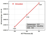
도 11은 스위칭 트랜지스터의 활성층 두께에 따라서 누설전류가 달라지는 것을 나타내는 도면.
도 12는 스위칭 트랜지스터의 게이트 절연막 두께에 따라서 누설전류가 달라지는 것을 나타내는 도면.
도 13은 스위칭 트랜지스터의 실시 예를 나타내는 단면도.
도 14는 스위칭 트랜지스터의 LDD 도핑 농도에 따라서 누설전류가 달라지는 것을 나타내는 도면.
도 15는 스위칭 트랜지스터의 다른 실시 예를 나타내는 단면도.
도 16은 스위칭 트랜지스터의 광차단막 유무에 따라서 누설전류가 달라지는 것을 나타내는 도면.
도 17은 스위칭 트랜지스터의 또 다른 실시 예를 나타내는 단면도.
도 18은 듀얼 게이트 구조와 싱글 게이트 구조에서의 누설전류의 차이를 나타내는 도면.
도 19는 본 발명에 의한 스토리지 커패시터의 제1 실시 예를 나타내는 도면.
도 20은 본 발명에 의한 스토리지 커패시터의 제2 실시 예를 나타내는 도면.
도 21은 스토리지 커패시터의 용량에 따라서 누설전류가 달라지는 것을 나타내는 도면.
12 : 데이터 구동회로 13 : 게이트 구동회로
14 : 데이터라인부 15 : 게이트라인부
Claims (19)
- 데이터라인 및 게이트 라인에 연결된 픽셀들;
상기 데이터라인에 데이터전압을 공급하는 데이터 구동회로;
상기 게이트라인에 스캔신호를 공급하는 게이트 구동회로; 및
상기 데이터 구동회로와 상기 게이트 구동회로의 동작 타이밍을 제어하는 타이밍 콘트롤러를 포함하고,
상기 픽셀들 각각은
유기발광다이오드;
게이트에 인가되는 게이트 전압에 따라서 상기 유기발광다이오드에 흐르는 전류를 조절하는 구동트랜지스터;
상기 스캔신호에 응답하여 상기 데이터라인으로부터 제공받는 상기 데이터전압을 상기 구동트랜지스터의 게이트에 공급하는 스위칭 트랜지스터; 및
상기 구동트랜지스터의 게이트 전압을 유지하는 스토리지 커패시터를 포함하고,
상기 구동트랜지스터의 활성층은 저온 폴리 실리콘을 포함하고, 상기 스위칭 트랜지스터의 활성층은 산화물 반도체를 포함하고,
상기 구동트랜지스터는,
폴리 실리콘 활성층 상에 형성된 게이트 절연막(GI);
상기 게이트 절연막(GI) 상에 형성된 제1 게이트층(GATE1);
상기 제1 게이트층(GATE1)을 덮도록 순차적으로 적층되는, SiO2로 형성된 제1 절연막(ILD1), SiNx으로 형성된 제2 절연막(ILD2), SiO2로 형성된 제3 절연막(ILD3),
상기 제1 내지 제3 절연막(ILD1~ILD3)을 관통하여 상기 저온 폴리 실리콘 활성층의 일부 영역에 각각 접속되는 소스 전극 및 드레인 전극;을 포함하고,
상기 스위칭 트랜지스터는,
상기 게이트 절연막(GI) 상에 제2 게이트층(GATE2)이 형성되고;
상기 제2 게이트층(GATE2) 상에 상기 SiO2로 형성된 제3 절연막(ILD3)이 형성되고;
상기 제3 절연막(ILD3) 상에 상기 산화물 반도체 활성층이 형성되고;
상기 제3 절연막(ILD3) 상에서 상기 산화물 반도체 활성층의 일부 영역에 각각 접속되는 소스 전극 및 드레인 전극;을 포함하고,
상기 타이밍 콘트롤러는 상기 픽셀들이 1Hz 이상 10Hz이하의 프레임 레이트로 구동되도록 상기 데이터 구동회로와 상기 게이트 구동회로를 제어하고,
상기 스토리지 커패시터가 형성되는 영역의 상기 게이트 절연막(GI)의 유전율은 인접하는 영역의 상기 게이트 절연막(GI)의 유전율보다 높은 유기발광다이오드 표시장치. - 제 1 항에 있어서,
상기 산화물 반도체는 산화아연(ZnO) 및 갈륨-인듐-아연(GIZO)으로 구성된 군에서 선택된 적어도 어느 하나인 유기발광다이오드 표시장치.
- 삭제
- 삭제
- 삭제
- 삭제
- 삭제
- 삭제
- 삭제
- 삭제
- 삭제
- 삭제
- 삭제
- 삭제
- 삭제
- 삭제
- 제 1 항에 있어서,
상기 스토리지 커패시터는 서로 적층되는 제1 및 제2 스토리지 커패시터를 포함하고,
상기 제1 스토리지 커패시터는
제1 금속층;
제2 금속층; 및
상기 제1 및 제2 금속층 사이에 개재되는 상기 게이트 절연막을 포함하고,
상기 제2 스토리지 커패시터는
상기 제2 금속층;
제3 금속층; 및
상기 제2 및 제3 금속층 사이에 개재되는 절연막을 포함하는 유기발광다이오드 표시장치.
- 제 1 항에 있어서,
상기 스토리지 커패시터는
제1 금속층;
제2 금속층; 및
상기 제1 및 제2 금속층 사이에 개재되는 상기 게이트 절연막을 포함하는 유기발광다이오드 표시장치.
- 픽셀들을 구동하는 유기발광다이오드 표시장치에 있어서,
상기 픽셀들 각각은
유기발광다이오드;
게이트에 인가되는 게이트 전압에 따라서 상기 유기발광다이오드에 흐르는 전류를 조절하는 구동트랜지스터(DT);
스캔펄스에 응답하여 데이터라인으로부터 제공받는 데이터전압을 상기 구동트랜지스터(DT)의 게이트에 공급하는 스위칭 트랜지스터(ST);
상기 구동트랜지스터(DT)의 게이트 전압을 유지하는 스토리지 커패시터를 포함하고,
상기 구동트랜지스터(DT)는,
기판 상에 저온 폴리 실리콘으로 형성된 DT 활성화층;
상기 DT 활성화층에 형성된 DT 소스 및 DT 드레인;
상기 DT 활성화층 상에 형성된 게이트 절연층;
상기 게이트 절연층 상에 형성된 DT 게이트;
상기 DT 게이트 위에 순차적으로 적층되는, SiO2로 형성된 제1 절연층(ILD1), SiNx으로 형성된 제2 절연층(ILD2), SiO2로 형성된 제3 절연층(ILD3);
상기 제1 내지 제3 절연층(ILD1~ILD3)을 관통하여 상기 DT 소스 및 DT 드레인에 각각 접속되는 소스 전극 및 드레인 전극;을 포함하고,
상기 스위칭트랜지스터(ST)는,
상기 게이트 절연층 상에 형성되는 ST 게이트;
상기 ST 게이트 상에 형성되는 SiO2로 형성된 제3 절연층(ILD3);
상기 제3 절연층(ILD3) 상에 산화물 반도체 물질로 형성된 ST 활성화층;
상기 제3 절연층(ILD3) 상에서 상기 ST 활성화층의 일부 영역에 각각 접속되는 ST 소스 및 ST 드레인;을 포함하고,
ST 소스와 ST 드레인은 모두 상기 DT 게이트와는 반대편에 있는 상기 ST 활성화층에 접촉되고,
상기 스토리지 커패시터가 형성되는 영역의 상기 게이트 절연층의 유전율은 인접하는 영역의 상기 게이트 절연층의 유전율보다 높은 유기발광다이오드 표시장치.
Priority Applications (5)
| Application Number | Priority Date | Filing Date | Title |
|---|---|---|---|
| KR1020140076096A KR102298336B1 (ko) | 2014-06-20 | 2014-06-20 | 유기발광다이오드 표시장치 |
| US14/740,564 US9412303B2 (en) | 2014-06-20 | 2015-06-16 | Reduced off current switching transistor in an organic light-emitting diode display device |
| EP15172514.0A EP2958102A1 (en) | 2014-06-20 | 2015-06-17 | Reduced off current switching transistor in an organic light-emitting diode display device |
| CN201510344910.6A CN105225633B (zh) | 2014-06-20 | 2015-06-19 | 有机发光二极管显示装置 |
| US15/169,251 US9721509B2 (en) | 2014-06-20 | 2016-05-31 | Reduced off current switching transistor in an organic light-emitting diode display device |
Applications Claiming Priority (1)
| Application Number | Priority Date | Filing Date | Title |
|---|---|---|---|
| KR1020140076096A KR102298336B1 (ko) | 2014-06-20 | 2014-06-20 | 유기발광다이오드 표시장치 |
Publications (2)
| Publication Number | Publication Date |
|---|---|
| KR20150146117A KR20150146117A (ko) | 2015-12-31 |
| KR102298336B1 true KR102298336B1 (ko) | 2021-09-08 |
Family
ID=53434266
Family Applications (1)
| Application Number | Title | Priority Date | Filing Date |
|---|---|---|---|
| KR1020140076096A Active KR102298336B1 (ko) | 2014-06-20 | 2014-06-20 | 유기발광다이오드 표시장치 |
Country Status (4)
| Country | Link |
|---|---|
| US (2) | US9412303B2 (ko) |
| EP (1) | EP2958102A1 (ko) |
| KR (1) | KR102298336B1 (ko) |
| CN (1) | CN105225633B (ko) |
Families Citing this family (57)
| Publication number | Priority date | Publication date | Assignee | Title |
|---|---|---|---|---|
| KR102206287B1 (ko) * | 2014-06-13 | 2021-01-25 | 삼성디스플레이 주식회사 | 표시 장치 및 표시 장치의 구동 방법 |
| KR20160011248A (ko) * | 2014-07-21 | 2016-02-01 | 삼성디스플레이 주식회사 | 표시 패널 및 이를 포함하는 유기 발광 표시 장치 |
| CN106558538B (zh) * | 2015-09-18 | 2019-09-13 | 鸿富锦精密工业(深圳)有限公司 | 阵列基板、显示装置及阵列基板的制备方法 |
| WO2021035416A1 (zh) | 2019-08-23 | 2021-03-04 | 京东方科技集团股份有限公司 | 显示装置及其制备方法 |
| CN105185816A (zh) | 2015-10-15 | 2015-12-23 | 京东方科技集团股份有限公司 | 阵列基板及其制造方法、显示装置 |
| US11600234B2 (en) | 2015-10-15 | 2023-03-07 | Ordos Yuansheng Optoelectronics Co., Ltd. | Display substrate and driving method thereof |
| WO2021035529A1 (zh) | 2019-08-27 | 2021-03-04 | 京东方科技集团股份有限公司 | 电子装置基板及其制作方法、电子装置 |
| WO2021035405A1 (zh) | 2019-08-23 | 2021-03-04 | 京东方科技集团股份有限公司 | 显示装置及其制造方法和驱动基板 |
| KR102457757B1 (ko) * | 2015-10-28 | 2022-10-24 | 삼성디스플레이 주식회사 | 화소 회로 및 이를 포함하는 유기 발광 표시 장치 |
| JP2017116576A (ja) * | 2015-12-21 | 2017-06-29 | 株式会社ジャパンディスプレイ | 表示装置 |
| CN105489615B (zh) * | 2016-01-13 | 2019-03-08 | 深圳市华星光电技术有限公司 | 用于amoled的薄膜晶体管阵列基板及其制造方法 |
| KR102617379B1 (ko) | 2016-05-02 | 2023-12-27 | 삼성디스플레이 주식회사 | 유기발광 표시장치 및 이의 제조 방법 |
| JP6668160B2 (ja) * | 2016-05-06 | 2020-03-18 | 株式会社ジャパンディスプレイ | 表示装置の製造方法 |
| CN116229869A (zh) | 2016-06-20 | 2023-06-06 | 索尼公司 | 显示设备和电子设备 |
| KR102561294B1 (ko) * | 2016-07-01 | 2023-08-01 | 삼성디스플레이 주식회사 | 화소 및 스테이지 회로와 이를 가지는 유기전계발광 표시장치 |
| KR20180004370A (ko) * | 2016-07-01 | 2018-01-11 | 삼성디스플레이 주식회사 | 화소 및 스테이지 회로와 이를 가지는 유기전계발광 표시장치 |
| CN114155812A (zh) * | 2016-08-30 | 2022-03-08 | 索尼半导体解决方案公司 | 显示装置和电子设备 |
| US10339855B2 (en) | 2016-08-30 | 2019-07-02 | Apple, Inc. | Device and method for improved LED driving |
| KR102795156B1 (ko) * | 2016-08-31 | 2025-04-15 | 엘지디스플레이 주식회사 | 유기발광 표시장치 |
| JP2018063351A (ja) * | 2016-10-13 | 2018-04-19 | 株式会社ジャパンディスプレイ | 有機el表示装置及び有機el表示装置の駆動方法 |
| KR102516721B1 (ko) * | 2016-11-30 | 2023-03-30 | 엘지디스플레이 주식회사 | 트랜지스터 기판, 이를 이용한 유기발광표시패널 및 그 제조 방법과, 이를 이용한 유기발광표시장치 |
| KR102541552B1 (ko) | 2016-11-30 | 2023-06-07 | 엘지디스플레이 주식회사 | 트랜지스터 기판 및 이를 이용한 유기발광표시패널과 유기발광표시장치 |
| KR102566551B1 (ko) | 2016-12-05 | 2023-08-14 | 삼성디스플레이주식회사 | 표시장치 및 그의 구동방법 |
| KR102775758B1 (ko) | 2017-02-24 | 2025-03-07 | 삼성디스플레이 주식회사 | 화소 및 이를 가지는 유기전계발광 표시장치 |
| US10672338B2 (en) * | 2017-03-24 | 2020-06-02 | Apple Inc. | Organic light-emitting diode display with external compensation and anode reset |
| KR102309097B1 (ko) | 2017-04-10 | 2021-10-07 | 삼성디스플레이 주식회사 | 표시장치 및 그의 구동 방법 |
| TWI620111B (zh) * | 2017-05-19 | 2018-04-01 | 友達光電股份有限公司 | 顯示裝置與其操作方法 |
| CN107293552A (zh) * | 2017-06-05 | 2017-10-24 | 深圳市华星光电技术有限公司 | 一种阵列基板及显示装置 |
| KR102464131B1 (ko) | 2017-06-30 | 2022-11-04 | 엘지디스플레이 주식회사 | 전계발광 표시장치 |
| CN107818991B (zh) * | 2017-10-23 | 2020-06-05 | 京东方科技集团股份有限公司 | 一种阵列基板及其制备方法、显示面板 |
| KR102547410B1 (ko) * | 2017-10-31 | 2023-06-22 | 엘지디스플레이 주식회사 | 발광 표시 장치 |
| KR102328441B1 (ko) * | 2017-11-10 | 2021-11-17 | 엘지디스플레이 주식회사 | 유기 발광 표시 장치 |
| CN108257975B (zh) * | 2018-01-02 | 2022-10-04 | 京东方科技集团股份有限公司 | 阵列基板及其制备方法、显示装置、薄膜晶体管的制备方法 |
| KR102509795B1 (ko) * | 2018-05-03 | 2023-03-15 | 삼성디스플레이 주식회사 | 표시 장치 및 이를 이용한 표시 패널의 구동 방법 |
| KR102565412B1 (ko) | 2018-08-28 | 2023-08-10 | 삼성디스플레이 주식회사 | 유기 발광 표시 장치 |
| KR102482335B1 (ko) | 2018-10-04 | 2022-12-29 | 삼성디스플레이 주식회사 | 표시 장치 및 이를 이용한 표시 패널의 구동 방법 |
| CN109285502B (zh) * | 2018-11-14 | 2020-06-16 | 武汉华星光电半导体显示技术有限公司 | Oled显示面板 |
| KR102583819B1 (ko) * | 2018-12-18 | 2023-10-04 | 삼성디스플레이 주식회사 | 표시 장치 및 이를 이용한 표시 패널의 구동 방법 |
| KR102678855B1 (ko) | 2019-01-28 | 2024-06-28 | 삼성디스플레이 주식회사 | 표시 장치 및 이를 이용한 표시 패널의 구동 방법 |
| KR20200107012A (ko) * | 2019-03-05 | 2020-09-16 | 삼성디스플레이 주식회사 | 표시 장치 및 그 제조 방법 |
| CN110299322B (zh) * | 2019-07-03 | 2022-03-08 | 京东方科技集团股份有限公司 | 一种显示基板及其制作方法、显示装置 |
| US11569482B2 (en) | 2019-08-23 | 2023-01-31 | Beijing Boe Technology Development Co., Ltd. | Display panel and manufacturing method thereof, display device |
| CN116994527A (zh) * | 2019-08-23 | 2023-11-03 | 京东方科技集团股份有限公司 | 显示装置及其制备方法 |
| EP4020447B1 (en) | 2019-08-23 | 2024-03-27 | BOE Technology Group Co., Ltd. | Pixel circuit and driving method therefor, and display substrate and driving method therefor, and display device |
| US11930664B2 (en) | 2019-08-23 | 2024-03-12 | Boe Technology Group Co., Ltd. | Display device with transistors oriented in directions intersecting direction of driving transistor and manufacturing method thereof |
| US12266303B2 (en) | 2019-08-23 | 2025-04-01 | Boe Technology Group Co., Ltd. | Display device and manufacturing method thereof |
| CN110707095A (zh) * | 2019-09-04 | 2020-01-17 | 深圳市华星光电半导体显示技术有限公司 | 显示面板 |
| CN118763123A (zh) * | 2019-09-24 | 2024-10-11 | 乐金显示有限公司 | 薄膜晶体管及其基板及包括该薄膜晶体管的显示设备 |
| KR102615673B1 (ko) * | 2019-12-26 | 2023-12-18 | 엘지디스플레이 주식회사 | 표시장치 |
| CN111682047A (zh) * | 2020-06-12 | 2020-09-18 | 福建华佳彩有限公司 | 一种补偿电容结构及其容值的提升方法 |
| CN111627387B (zh) | 2020-06-24 | 2022-09-02 | 京东方科技集团股份有限公司 | 像素驱动电路及其驱动方法、显示面板及显示装置 |
| JP7030162B1 (ja) * | 2020-08-20 | 2022-03-04 | シャープ株式会社 | 制御装置、自発光素子を備える表示装置、制御方法および制御プログラム |
| JP2022035402A (ja) * | 2020-08-20 | 2022-03-04 | シャープ株式会社 | 表示装置、表示駆動方法、及び表示駆動プログラム |
| CN112034616B (zh) * | 2020-08-31 | 2022-06-03 | 同济大学 | 用于可扩展低能激光超高速扫描的可变透镜及应用 |
| CN112071259B (zh) * | 2020-09-15 | 2021-11-23 | 武汉华星光电半导体显示技术有限公司 | 像素电路及显示面板 |
| CN116097924A (zh) * | 2021-03-11 | 2023-05-09 | 京东方科技集团股份有限公司 | 阵列基板及其显示面板和显示装置 |
| CN116133479A (zh) * | 2021-04-23 | 2023-05-16 | 武汉天马微电子有限公司 | 一种显示面板和显示装置 |
Citations (7)
| Publication number | Priority date | Publication date | Assignee | Title |
|---|---|---|---|---|
| JP2008042010A (ja) * | 2006-08-08 | 2008-02-21 | Sharp Corp | 半導体装置、半導体装置の製造方法、及び、電子装置 |
| JP2008047913A (ja) | 2006-08-15 | 2008-02-28 | Toppoly Optoelectronics Corp | 薄膜トランジスタデバイスを含む画像表示システムとその製造方法 |
| JP2008205330A (ja) | 2007-02-22 | 2008-09-04 | Semiconductor Energy Lab Co Ltd | 半導体装置 |
| JP2012022335A (ja) * | 2011-10-03 | 2012-02-02 | Semiconductor Energy Lab Co Ltd | 半導体装置 |
| US20130015448A1 (en) | 2011-07-14 | 2013-01-17 | Chao-Shun Yang | Semiconductor device and electroluminescent device and method of making the same |
| US20130049000A1 (en) | 2011-08-26 | 2013-02-28 | Shou-Peng Weng | Semiconductor device and method of making the same |
| US20130168666A1 (en) * | 2011-12-30 | 2013-07-04 | Industrial Technology Research Institute | Semiconductor device and method of forming the same |
Family Cites Families (18)
| Publication number | Priority date | Publication date | Assignee | Title |
|---|---|---|---|---|
| TW591584B (en) * | 1999-10-21 | 2004-06-11 | Semiconductor Energy Lab | Active matrix type display device |
| JP3899886B2 (ja) * | 2001-10-10 | 2007-03-28 | 株式会社日立製作所 | 画像表示装置 |
| US6852997B2 (en) * | 2001-10-30 | 2005-02-08 | Semiconductor Energy Laboratory Co., Ltd. | Light emitting device |
| US7915723B2 (en) * | 2004-01-29 | 2011-03-29 | Casio Computer Co., Ltd. | Transistor array, manufacturing method thereof and image processor |
| KR100600878B1 (ko) * | 2004-06-29 | 2006-07-14 | 삼성에스디아이 주식회사 | 박막트랜지스터 및 그 제조방법 |
| US7646367B2 (en) * | 2005-01-21 | 2010-01-12 | Semiconductor Energy Laboratory Co., Ltd. | Semiconductor device, display device and electronic apparatus |
| US8681077B2 (en) * | 2005-03-18 | 2014-03-25 | Semiconductor Energy Laboratory Co., Ltd. | Semiconductor device, and display device, driving method and electronic apparatus thereof |
| KR20070081829A (ko) * | 2006-02-14 | 2007-08-20 | 삼성전자주식회사 | 유기 발광 표시 장치 및 그 제조 방법 |
| US8040334B2 (en) * | 2006-12-29 | 2011-10-18 | 02Micro International Limited | Method of driving display device |
| KR101596935B1 (ko) * | 2008-12-26 | 2016-02-24 | 엘지디스플레이 주식회사 | 유기전계 발광소자 및 이의 제조 방법 |
| KR20180014255A (ko) * | 2009-11-13 | 2018-02-07 | 가부시키가이샤 한도오따이 에네루기 켄큐쇼 | 표시 장치 및 이 표시 장치를 구비한 전자 기기 |
| KR101117739B1 (ko) * | 2010-03-15 | 2012-02-24 | 삼성모바일디스플레이주식회사 | 박막 트랜지스터 및 그 제조방법 |
| WO2011135920A1 (ja) * | 2010-04-30 | 2011-11-03 | シャープ株式会社 | 回路基板、表示装置および回路基板の製造方法 |
| JP2014130336A (ja) | 2012-11-30 | 2014-07-10 | Semiconductor Energy Lab Co Ltd | 表示装置 |
| KR102023185B1 (ko) * | 2013-07-08 | 2019-11-05 | 삼성디스플레이 주식회사 | 유기 발광 표시 장치 |
| US9818765B2 (en) | 2013-08-26 | 2017-11-14 | Apple Inc. | Displays with silicon and semiconducting oxide thin-film transistors |
| US9412799B2 (en) | 2013-08-26 | 2016-08-09 | Apple Inc. | Display driver circuitry for liquid crystal displays with semiconducting-oxide thin-film transistors |
| US10186528B2 (en) | 2014-02-24 | 2019-01-22 | Lg Display Co., Ltd. | Thin film transistor substrate and display using the same |
-
2014
- 2014-06-20 KR KR1020140076096A patent/KR102298336B1/ko active Active
-
2015
- 2015-06-16 US US14/740,564 patent/US9412303B2/en active Active
- 2015-06-17 EP EP15172514.0A patent/EP2958102A1/en not_active Ceased
- 2015-06-19 CN CN201510344910.6A patent/CN105225633B/zh active Active
-
2016
- 2016-05-31 US US15/169,251 patent/US9721509B2/en active Active
Patent Citations (7)
| Publication number | Priority date | Publication date | Assignee | Title |
|---|---|---|---|---|
| JP2008042010A (ja) * | 2006-08-08 | 2008-02-21 | Sharp Corp | 半導体装置、半導体装置の製造方法、及び、電子装置 |
| JP2008047913A (ja) | 2006-08-15 | 2008-02-28 | Toppoly Optoelectronics Corp | 薄膜トランジスタデバイスを含む画像表示システムとその製造方法 |
| JP2008205330A (ja) | 2007-02-22 | 2008-09-04 | Semiconductor Energy Lab Co Ltd | 半導体装置 |
| US20130015448A1 (en) | 2011-07-14 | 2013-01-17 | Chao-Shun Yang | Semiconductor device and electroluminescent device and method of making the same |
| US20130049000A1 (en) | 2011-08-26 | 2013-02-28 | Shou-Peng Weng | Semiconductor device and method of making the same |
| JP2012022335A (ja) * | 2011-10-03 | 2012-02-02 | Semiconductor Energy Lab Co Ltd | 半導体装置 |
| US20130168666A1 (en) * | 2011-12-30 | 2013-07-04 | Industrial Technology Research Institute | Semiconductor device and method of forming the same |
Also Published As
| Publication number | Publication date |
|---|---|
| CN105225633B (zh) | 2018-11-16 |
| EP2958102A1 (en) | 2015-12-23 |
| US9721509B2 (en) | 2017-08-01 |
| US20150371589A1 (en) | 2015-12-24 |
| CN105225633A (zh) | 2016-01-06 |
| US9412303B2 (en) | 2016-08-09 |
| KR20150146117A (ko) | 2015-12-31 |
| US20160275867A1 (en) | 2016-09-22 |
Similar Documents
| Publication | Publication Date | Title |
|---|---|---|
| KR102298336B1 (ko) | 유기발광다이오드 표시장치 | |
| US11915651B2 (en) | Electroluminescent display | |
| US11069297B2 (en) | Pixel circuit and method of driving the same, display panel, and display apparatus | |
| US10312312B2 (en) | Display device having LTPS and oxide TFTs integrated on the same substrate | |
| KR101962860B1 (ko) | 조절가능한 리프레시 레이트로 구동되는 선택적인 부분들을 포함하는 디스플레이 및 이를 구동하는 방법 | |
| US9214506B2 (en) | Pixel unit driving circuit, method for driving pixel unit driving circuit and display device | |
| KR101773661B1 (ko) | 디스플레이 백플레인 및 이의 제조 방법 | |
| US9595546B2 (en) | Display backplane and method of fabricating the same | |
| WO2019137105A1 (zh) | 像素电路、驱动方法、电致发光显示面板及显示装置 | |
| US7889160B2 (en) | Organic light-emitting diode display device and driving method thereof | |
| US8941309B2 (en) | Voltage-driven pixel circuit, driving method thereof and display panel | |
| US9576525B2 (en) | AMOLED pixel unit, method for driving the same, and display device | |
| US9875690B2 (en) | Pixel circuit, display substrate and display panel | |
| EP3113226A1 (en) | Display backplane and method for manufacturing same | |
| WO2015188533A1 (zh) | 像素驱动电路、驱动方法、阵列基板及显示装置 | |
| US9916792B2 (en) | Pixel driving circuit and driving method thereof and display apparatus | |
| KR102076845B1 (ko) | 유기발광다이오드 표시장치의 구동방법 | |
| KR102050381B1 (ko) | 유기발광다이오드 표시장치의 구동트랜지스터 특성 검출방법 | |
| KR102348657B1 (ko) | 전계 발광 표시 장치 | |
| KR20160007779A (ko) | 유기발광다이오드 표시장치 및 그의 구동방법 | |
| KR20250030569A (ko) | 표시 장치 | |
| KR20250072649A (ko) | 표시 장치 | |
| KR20230092488A (ko) | 패널 회로 및 패널 회로를 포함하는 표시 장치 |
Legal Events
| Date | Code | Title | Description |
|---|---|---|---|
| PA0109 | Patent application |
Patent event code: PA01091R01D Comment text: Patent Application Patent event date: 20140620 |
|
| PG1501 | Laying open of application | ||
| A201 | Request for examination | ||
| PA0201 | Request for examination |
Patent event code: PA02012R01D Patent event date: 20190508 Comment text: Request for Examination of Application Patent event code: PA02011R01I Patent event date: 20140620 Comment text: Patent Application |
|
| E902 | Notification of reason for refusal | ||
| PE0902 | Notice of grounds for rejection |
Comment text: Notification of reason for refusal Patent event date: 20200731 Patent event code: PE09021S01D |
|
| AMND | Amendment | ||
| E601 | Decision to refuse application | ||
| PE0601 | Decision on rejection of patent |
Patent event date: 20210423 Comment text: Decision to Refuse Application Patent event code: PE06012S01D Patent event date: 20200731 Comment text: Notification of reason for refusal Patent event code: PE06011S01I |
|
| AMND | Amendment | ||
| PX0901 | Re-examination |
Patent event code: PX09011S01I Patent event date: 20210423 Comment text: Decision to Refuse Application Patent event code: PX09012R01I Patent event date: 20201005 Comment text: Amendment to Specification, etc. |
|
| PX0701 | Decision of registration after re-examination |
Patent event date: 20210630 Comment text: Decision to Grant Registration Patent event code: PX07013S01D Patent event date: 20210624 Comment text: Amendment to Specification, etc. Patent event code: PX07012R01I Patent event date: 20210423 Comment text: Decision to Refuse Application Patent event code: PX07011S01I Patent event date: 20201005 Comment text: Amendment to Specification, etc. Patent event code: PX07012R01I |
|
| X701 | Decision to grant (after re-examination) | ||
| GRNT | Written decision to grant | ||
| PR0701 | Registration of establishment |
Comment text: Registration of Establishment Patent event date: 20210831 Patent event code: PR07011E01D |
|
| PR1002 | Payment of registration fee |
Payment date: 20210901 End annual number: 3 Start annual number: 1 |
|
| PG1601 | Publication of registration | ||
| PR1001 | Payment of annual fee |
Payment date: 20240715 Start annual number: 4 End annual number: 4 |