KR102298336B1 - Organic Light Emitting diode Display - Google Patents
Organic Light Emitting diode Display Download PDFInfo
- Publication number
- KR102298336B1 KR102298336B1 KR1020140076096A KR20140076096A KR102298336B1 KR 102298336 B1 KR102298336 B1 KR 102298336B1 KR 1020140076096 A KR1020140076096 A KR 1020140076096A KR 20140076096 A KR20140076096 A KR 20140076096A KR 102298336 B1 KR102298336 B1 KR 102298336B1
- Authority
- KR
- South Korea
- Prior art keywords
- gate
- layer
- insulating layer
- driving
- transistor
- Prior art date
- Legal status (The legal status is an assumption and is not a legal conclusion. Google has not performed a legal analysis and makes no representation as to the accuracy of the status listed.)
- Active
Links
Images


Classifications
-
- G—PHYSICS
- G09—EDUCATION; CRYPTOGRAPHY; DISPLAY; ADVERTISING; SEALS
- G09G—ARRANGEMENTS OR CIRCUITS FOR CONTROL OF INDICATING DEVICES USING STATIC MEANS TO PRESENT VARIABLE INFORMATION
- G09G3/00—Control arrangements or circuits, of interest only in connection with visual indicators other than cathode-ray tubes
- G09G3/20—Control arrangements or circuits, of interest only in connection with visual indicators other than cathode-ray tubes for presentation of an assembly of a number of characters, e.g. a page, by composing the assembly by combination of individual elements arranged in a matrix no fixed position being assigned to or needed to be assigned to the individual characters or partial characters
- G09G3/22—Control arrangements or circuits, of interest only in connection with visual indicators other than cathode-ray tubes for presentation of an assembly of a number of characters, e.g. a page, by composing the assembly by combination of individual elements arranged in a matrix no fixed position being assigned to or needed to be assigned to the individual characters or partial characters using controlled light sources
- G09G3/30—Control arrangements or circuits, of interest only in connection with visual indicators other than cathode-ray tubes for presentation of an assembly of a number of characters, e.g. a page, by composing the assembly by combination of individual elements arranged in a matrix no fixed position being assigned to or needed to be assigned to the individual characters or partial characters using controlled light sources using electroluminescent panels
- G09G3/32—Control arrangements or circuits, of interest only in connection with visual indicators other than cathode-ray tubes for presentation of an assembly of a number of characters, e.g. a page, by composing the assembly by combination of individual elements arranged in a matrix no fixed position being assigned to or needed to be assigned to the individual characters or partial characters using controlled light sources using electroluminescent panels semiconductive, e.g. using light-emitting diodes [LED]
- G09G3/3208—Control arrangements or circuits, of interest only in connection with visual indicators other than cathode-ray tubes for presentation of an assembly of a number of characters, e.g. a page, by composing the assembly by combination of individual elements arranged in a matrix no fixed position being assigned to or needed to be assigned to the individual characters or partial characters using controlled light sources using electroluminescent panels semiconductive, e.g. using light-emitting diodes [LED] organic, e.g. using organic light-emitting diodes [OLED]
- G09G3/3225—Control arrangements or circuits, of interest only in connection with visual indicators other than cathode-ray tubes for presentation of an assembly of a number of characters, e.g. a page, by composing the assembly by combination of individual elements arranged in a matrix no fixed position being assigned to or needed to be assigned to the individual characters or partial characters using controlled light sources using electroluminescent panels semiconductive, e.g. using light-emitting diodes [LED] organic, e.g. using organic light-emitting diodes [OLED] using an active matrix
- G09G3/3258—Control arrangements or circuits, of interest only in connection with visual indicators other than cathode-ray tubes for presentation of an assembly of a number of characters, e.g. a page, by composing the assembly by combination of individual elements arranged in a matrix no fixed position being assigned to or needed to be assigned to the individual characters or partial characters using controlled light sources using electroluminescent panels semiconductive, e.g. using light-emitting diodes [LED] organic, e.g. using organic light-emitting diodes [OLED] using an active matrix with pixel circuitry controlling the voltage across the light-emitting element
-
- G—PHYSICS
- G09—EDUCATION; CRYPTOGRAPHY; DISPLAY; ADVERTISING; SEALS
- G09G—ARRANGEMENTS OR CIRCUITS FOR CONTROL OF INDICATING DEVICES USING STATIC MEANS TO PRESENT VARIABLE INFORMATION
- G09G3/00—Control arrangements or circuits, of interest only in connection with visual indicators other than cathode-ray tubes
- G09G3/20—Control arrangements or circuits, of interest only in connection with visual indicators other than cathode-ray tubes for presentation of an assembly of a number of characters, e.g. a page, by composing the assembly by combination of individual elements arranged in a matrix no fixed position being assigned to or needed to be assigned to the individual characters or partial characters
- G09G3/22—Control arrangements or circuits, of interest only in connection with visual indicators other than cathode-ray tubes for presentation of an assembly of a number of characters, e.g. a page, by composing the assembly by combination of individual elements arranged in a matrix no fixed position being assigned to or needed to be assigned to the individual characters or partial characters using controlled light sources
- G09G3/30—Control arrangements or circuits, of interest only in connection with visual indicators other than cathode-ray tubes for presentation of an assembly of a number of characters, e.g. a page, by composing the assembly by combination of individual elements arranged in a matrix no fixed position being assigned to or needed to be assigned to the individual characters or partial characters using controlled light sources using electroluminescent panels
- G09G3/32—Control arrangements or circuits, of interest only in connection with visual indicators other than cathode-ray tubes for presentation of an assembly of a number of characters, e.g. a page, by composing the assembly by combination of individual elements arranged in a matrix no fixed position being assigned to or needed to be assigned to the individual characters or partial characters using controlled light sources using electroluminescent panels semiconductive, e.g. using light-emitting diodes [LED]
- G09G3/3208—Control arrangements or circuits, of interest only in connection with visual indicators other than cathode-ray tubes for presentation of an assembly of a number of characters, e.g. a page, by composing the assembly by combination of individual elements arranged in a matrix no fixed position being assigned to or needed to be assigned to the individual characters or partial characters using controlled light sources using electroluminescent panels semiconductive, e.g. using light-emitting diodes [LED] organic, e.g. using organic light-emitting diodes [OLED]
- G09G3/3225—Control arrangements or circuits, of interest only in connection with visual indicators other than cathode-ray tubes for presentation of an assembly of a number of characters, e.g. a page, by composing the assembly by combination of individual elements arranged in a matrix no fixed position being assigned to or needed to be assigned to the individual characters or partial characters using controlled light sources using electroluminescent panels semiconductive, e.g. using light-emitting diodes [LED] organic, e.g. using organic light-emitting diodes [OLED] using an active matrix
- G09G3/3233—Control arrangements or circuits, of interest only in connection with visual indicators other than cathode-ray tubes for presentation of an assembly of a number of characters, e.g. a page, by composing the assembly by combination of individual elements arranged in a matrix no fixed position being assigned to or needed to be assigned to the individual characters or partial characters using controlled light sources using electroluminescent panels semiconductive, e.g. using light-emitting diodes [LED] organic, e.g. using organic light-emitting diodes [OLED] using an active matrix with pixel circuitry controlling the current through the light-emitting element
-
- G—PHYSICS
- G09—EDUCATION; CRYPTOGRAPHY; DISPLAY; ADVERTISING; SEALS
- G09G—ARRANGEMENTS OR CIRCUITS FOR CONTROL OF INDICATING DEVICES USING STATIC MEANS TO PRESENT VARIABLE INFORMATION
- G09G3/00—Control arrangements or circuits, of interest only in connection with visual indicators other than cathode-ray tubes
- G09G3/20—Control arrangements or circuits, of interest only in connection with visual indicators other than cathode-ray tubes for presentation of an assembly of a number of characters, e.g. a page, by composing the assembly by combination of individual elements arranged in a matrix no fixed position being assigned to or needed to be assigned to the individual characters or partial characters
- G09G3/22—Control arrangements or circuits, of interest only in connection with visual indicators other than cathode-ray tubes for presentation of an assembly of a number of characters, e.g. a page, by composing the assembly by combination of individual elements arranged in a matrix no fixed position being assigned to or needed to be assigned to the individual characters or partial characters using controlled light sources
- G09G3/30—Control arrangements or circuits, of interest only in connection with visual indicators other than cathode-ray tubes for presentation of an assembly of a number of characters, e.g. a page, by composing the assembly by combination of individual elements arranged in a matrix no fixed position being assigned to or needed to be assigned to the individual characters or partial characters using controlled light sources using electroluminescent panels
- G09G3/32—Control arrangements or circuits, of interest only in connection with visual indicators other than cathode-ray tubes for presentation of an assembly of a number of characters, e.g. a page, by composing the assembly by combination of individual elements arranged in a matrix no fixed position being assigned to or needed to be assigned to the individual characters or partial characters using controlled light sources using electroluminescent panels semiconductive, e.g. using light-emitting diodes [LED]
- G09G3/3208—Control arrangements or circuits, of interest only in connection with visual indicators other than cathode-ray tubes for presentation of an assembly of a number of characters, e.g. a page, by composing the assembly by combination of individual elements arranged in a matrix no fixed position being assigned to or needed to be assigned to the individual characters or partial characters using controlled light sources using electroluminescent panels semiconductive, e.g. using light-emitting diodes [LED] organic, e.g. using organic light-emitting diodes [OLED]
- G09G3/3225—Control arrangements or circuits, of interest only in connection with visual indicators other than cathode-ray tubes for presentation of an assembly of a number of characters, e.g. a page, by composing the assembly by combination of individual elements arranged in a matrix no fixed position being assigned to or needed to be assigned to the individual characters or partial characters using controlled light sources using electroluminescent panels semiconductive, e.g. using light-emitting diodes [LED] organic, e.g. using organic light-emitting diodes [OLED] using an active matrix
- G09G3/3233—Control arrangements or circuits, of interest only in connection with visual indicators other than cathode-ray tubes for presentation of an assembly of a number of characters, e.g. a page, by composing the assembly by combination of individual elements arranged in a matrix no fixed position being assigned to or needed to be assigned to the individual characters or partial characters using controlled light sources using electroluminescent panels semiconductive, e.g. using light-emitting diodes [LED] organic, e.g. using organic light-emitting diodes [OLED] using an active matrix with pixel circuitry controlling the current through the light-emitting element
- G09G3/3241—Control arrangements or circuits, of interest only in connection with visual indicators other than cathode-ray tubes for presentation of an assembly of a number of characters, e.g. a page, by composing the assembly by combination of individual elements arranged in a matrix no fixed position being assigned to or needed to be assigned to the individual characters or partial characters using controlled light sources using electroluminescent panels semiconductive, e.g. using light-emitting diodes [LED] organic, e.g. using organic light-emitting diodes [OLED] using an active matrix with pixel circuitry controlling the current through the light-emitting element the current through the light-emitting element being set using a data current provided by the data driver, e.g. by using a two-transistor current mirror
- G09G3/325—Control arrangements or circuits, of interest only in connection with visual indicators other than cathode-ray tubes for presentation of an assembly of a number of characters, e.g. a page, by composing the assembly by combination of individual elements arranged in a matrix no fixed position being assigned to or needed to be assigned to the individual characters or partial characters using controlled light sources using electroluminescent panels semiconductive, e.g. using light-emitting diodes [LED] organic, e.g. using organic light-emitting diodes [OLED] using an active matrix with pixel circuitry controlling the current through the light-emitting element the current through the light-emitting element being set using a data current provided by the data driver, e.g. by using a two-transistor current mirror the data current flowing through the driving transistor during a setting phase, e.g. by using a switch for connecting the driving transistor to the data driver
-
- H—ELECTRICITY
- H10—SEMICONDUCTOR DEVICES; ELECTRIC SOLID-STATE DEVICES NOT OTHERWISE PROVIDED FOR
- H10D—INORGANIC ELECTRIC SEMICONDUCTOR DEVICES
- H10D30/00—Field-effect transistors [FET]
- H10D30/60—Insulated-gate field-effect transistors [IGFET]
- H10D30/67—Thin-film transistors [TFT]
- H10D30/6704—Thin-film transistors [TFT] having supplementary regions or layers in the thin films or in the insulated bulk substrates for controlling properties of the device
- H10D30/6706—Thin-film transistors [TFT] having supplementary regions or layers in the thin films or in the insulated bulk substrates for controlling properties of the device for preventing leakage current
-
- H—ELECTRICITY
- H10—SEMICONDUCTOR DEVICES; ELECTRIC SOLID-STATE DEVICES NOT OTHERWISE PROVIDED FOR
- H10D—INORGANIC ELECTRIC SEMICONDUCTOR DEVICES
- H10D30/00—Field-effect transistors [FET]
- H10D30/60—Insulated-gate field-effect transistors [IGFET]
- H10D30/67—Thin-film transistors [TFT]
- H10D30/6704—Thin-film transistors [TFT] having supplementary regions or layers in the thin films or in the insulated bulk substrates for controlling properties of the device
- H10D30/6723—Thin-film transistors [TFT] having supplementary regions or layers in the thin films or in the insulated bulk substrates for controlling properties of the device having light shields
-
- H—ELECTRICITY
- H10—SEMICONDUCTOR DEVICES; ELECTRIC SOLID-STATE DEVICES NOT OTHERWISE PROVIDED FOR
- H10D—INORGANIC ELECTRIC SEMICONDUCTOR DEVICES
- H10D86/00—Integrated devices formed in or on insulating or conducting substrates, e.g. formed in silicon-on-insulator [SOI] substrates or on stainless steel or glass substrates
- H10D86/40—Integrated devices formed in or on insulating or conducting substrates, e.g. formed in silicon-on-insulator [SOI] substrates or on stainless steel or glass substrates characterised by multiple TFTs
- H10D86/421—Integrated devices formed in or on insulating or conducting substrates, e.g. formed in silicon-on-insulator [SOI] substrates or on stainless steel or glass substrates characterised by multiple TFTs having a particular composition, shape or crystalline structure of the active layer
- H10D86/423—Integrated devices formed in or on insulating or conducting substrates, e.g. formed in silicon-on-insulator [SOI] substrates or on stainless steel or glass substrates characterised by multiple TFTs having a particular composition, shape or crystalline structure of the active layer comprising semiconductor materials not belonging to the Group IV, e.g. InGaZnO
-
- H—ELECTRICITY
- H10—SEMICONDUCTOR DEVICES; ELECTRIC SOLID-STATE DEVICES NOT OTHERWISE PROVIDED FOR
- H10D—INORGANIC ELECTRIC SEMICONDUCTOR DEVICES
- H10D86/00—Integrated devices formed in or on insulating or conducting substrates, e.g. formed in silicon-on-insulator [SOI] substrates or on stainless steel or glass substrates
- H10D86/40—Integrated devices formed in or on insulating or conducting substrates, e.g. formed in silicon-on-insulator [SOI] substrates or on stainless steel or glass substrates characterised by multiple TFTs
- H10D86/421—Integrated devices formed in or on insulating or conducting substrates, e.g. formed in silicon-on-insulator [SOI] substrates or on stainless steel or glass substrates characterised by multiple TFTs having a particular composition, shape or crystalline structure of the active layer
- H10D86/425—Integrated devices formed in or on insulating or conducting substrates, e.g. formed in silicon-on-insulator [SOI] substrates or on stainless steel or glass substrates characterised by multiple TFTs having a particular composition, shape or crystalline structure of the active layer having different crystal properties in different TFTs or within an individual TFT
-
- H—ELECTRICITY
- H10—SEMICONDUCTOR DEVICES; ELECTRIC SOLID-STATE DEVICES NOT OTHERWISE PROVIDED FOR
- H10D—INORGANIC ELECTRIC SEMICONDUCTOR DEVICES
- H10D86/00—Integrated devices formed in or on insulating or conducting substrates, e.g. formed in silicon-on-insulator [SOI] substrates or on stainless steel or glass substrates
- H10D86/40—Integrated devices formed in or on insulating or conducting substrates, e.g. formed in silicon-on-insulator [SOI] substrates or on stainless steel or glass substrates characterised by multiple TFTs
- H10D86/471—Integrated devices formed in or on insulating or conducting substrates, e.g. formed in silicon-on-insulator [SOI] substrates or on stainless steel or glass substrates characterised by multiple TFTs having different architectures, e.g. having both top-gate and bottom-gate TFTs
-
- H—ELECTRICITY
- H10—SEMICONDUCTOR DEVICES; ELECTRIC SOLID-STATE DEVICES NOT OTHERWISE PROVIDED FOR
- H10D—INORGANIC ELECTRIC SEMICONDUCTOR DEVICES
- H10D86/00—Integrated devices formed in or on insulating or conducting substrates, e.g. formed in silicon-on-insulator [SOI] substrates or on stainless steel or glass substrates
- H10D86/40—Integrated devices formed in or on insulating or conducting substrates, e.g. formed in silicon-on-insulator [SOI] substrates or on stainless steel or glass substrates characterised by multiple TFTs
- H10D86/60—Integrated devices formed in or on insulating or conducting substrates, e.g. formed in silicon-on-insulator [SOI] substrates or on stainless steel or glass substrates characterised by multiple TFTs wherein the TFTs are in active matrices
-
- G—PHYSICS
- G09—EDUCATION; CRYPTOGRAPHY; DISPLAY; ADVERTISING; SEALS
- G09G—ARRANGEMENTS OR CIRCUITS FOR CONTROL OF INDICATING DEVICES USING STATIC MEANS TO PRESENT VARIABLE INFORMATION
- G09G2300/00—Aspects of the constitution of display devices
- G09G2300/04—Structural and physical details of display devices
- G09G2300/0404—Matrix technologies
- G09G2300/0417—Special arrangements specific to the use of low carrier mobility technology
-
- G—PHYSICS
- G09—EDUCATION; CRYPTOGRAPHY; DISPLAY; ADVERTISING; SEALS
- G09G—ARRANGEMENTS OR CIRCUITS FOR CONTROL OF INDICATING DEVICES USING STATIC MEANS TO PRESENT VARIABLE INFORMATION
- G09G2300/00—Aspects of the constitution of display devices
- G09G2300/04—Structural and physical details of display devices
- G09G2300/0421—Structural details of the set of electrodes
- G09G2300/0426—Layout of electrodes and connections
-
- G—PHYSICS
- G09—EDUCATION; CRYPTOGRAPHY; DISPLAY; ADVERTISING; SEALS
- G09G—ARRANGEMENTS OR CIRCUITS FOR CONTROL OF INDICATING DEVICES USING STATIC MEANS TO PRESENT VARIABLE INFORMATION
- G09G2300/00—Aspects of the constitution of display devices
- G09G2300/04—Structural and physical details of display devices
- G09G2300/0421—Structural details of the set of electrodes
- G09G2300/043—Compensation electrodes or other additional electrodes in matrix displays related to distortions or compensation signals, e.g. for modifying TFT threshold voltage in column driver
-
- G—PHYSICS
- G09—EDUCATION; CRYPTOGRAPHY; DISPLAY; ADVERTISING; SEALS
- G09G—ARRANGEMENTS OR CIRCUITS FOR CONTROL OF INDICATING DEVICES USING STATIC MEANS TO PRESENT VARIABLE INFORMATION
- G09G2300/00—Aspects of the constitution of display devices
- G09G2300/08—Active matrix structure, i.e. with use of active elements, inclusive of non-linear two terminal elements, in the pixels together with light emitting or modulating elements
- G09G2300/0809—Several active elements per pixel in active matrix panels
- G09G2300/0819—Several active elements per pixel in active matrix panels used for counteracting undesired variations, e.g. feedback or autozeroing
-
- G—PHYSICS
- G09—EDUCATION; CRYPTOGRAPHY; DISPLAY; ADVERTISING; SEALS
- G09G—ARRANGEMENTS OR CIRCUITS FOR CONTROL OF INDICATING DEVICES USING STATIC MEANS TO PRESENT VARIABLE INFORMATION
- G09G2300/00—Aspects of the constitution of display devices
- G09G2300/08—Active matrix structure, i.e. with use of active elements, inclusive of non-linear two terminal elements, in the pixels together with light emitting or modulating elements
- G09G2300/0809—Several active elements per pixel in active matrix panels
- G09G2300/0842—Several active elements per pixel in active matrix panels forming a memory circuit, e.g. a dynamic memory with one capacitor
- G09G2300/0852—Several active elements per pixel in active matrix panels forming a memory circuit, e.g. a dynamic memory with one capacitor being a dynamic memory with more than one capacitor
-
- G—PHYSICS
- G09—EDUCATION; CRYPTOGRAPHY; DISPLAY; ADVERTISING; SEALS
- G09G—ARRANGEMENTS OR CIRCUITS FOR CONTROL OF INDICATING DEVICES USING STATIC MEANS TO PRESENT VARIABLE INFORMATION
- G09G2300/00—Aspects of the constitution of display devices
- G09G2300/08—Active matrix structure, i.e. with use of active elements, inclusive of non-linear two terminal elements, in the pixels together with light emitting or modulating elements
- G09G2300/0809—Several active elements per pixel in active matrix panels
- G09G2300/0842—Several active elements per pixel in active matrix panels forming a memory circuit, e.g. a dynamic memory with one capacitor
- G09G2300/0861—Several active elements per pixel in active matrix panels forming a memory circuit, e.g. a dynamic memory with one capacitor with additional control of the display period without amending the charge stored in a pixel memory, e.g. by means of additional select electrodes
-
- G—PHYSICS
- G09—EDUCATION; CRYPTOGRAPHY; DISPLAY; ADVERTISING; SEALS
- G09G—ARRANGEMENTS OR CIRCUITS FOR CONTROL OF INDICATING DEVICES USING STATIC MEANS TO PRESENT VARIABLE INFORMATION
- G09G2310/00—Command of the display device
- G09G2310/02—Addressing, scanning or driving the display screen or processing steps related thereto
- G09G2310/0262—The addressing of the pixel, in a display other than an active matrix LCD, involving the control of two or more scan electrodes or two or more data electrodes, e.g. pixel voltage dependent on signals of two data electrodes
-
- G—PHYSICS
- G09—EDUCATION; CRYPTOGRAPHY; DISPLAY; ADVERTISING; SEALS
- G09G—ARRANGEMENTS OR CIRCUITS FOR CONTROL OF INDICATING DEVICES USING STATIC MEANS TO PRESENT VARIABLE INFORMATION
- G09G2310/00—Command of the display device
- G09G2310/06—Details of flat display driving waveforms
-
- G—PHYSICS
- G09—EDUCATION; CRYPTOGRAPHY; DISPLAY; ADVERTISING; SEALS
- G09G—ARRANGEMENTS OR CIRCUITS FOR CONTROL OF INDICATING DEVICES USING STATIC MEANS TO PRESENT VARIABLE INFORMATION
- G09G2310/00—Command of the display device
- G09G2310/08—Details of timing specific for flat panels, other than clock recovery
-
- G—PHYSICS
- G09—EDUCATION; CRYPTOGRAPHY; DISPLAY; ADVERTISING; SEALS
- G09G—ARRANGEMENTS OR CIRCUITS FOR CONTROL OF INDICATING DEVICES USING STATIC MEANS TO PRESENT VARIABLE INFORMATION
- G09G2320/00—Control of display operating conditions
- G09G2320/02—Improving the quality of display appearance
- G09G2320/0247—Flicker reduction other than flicker reduction circuits used for single beam cathode-ray tubes
-
- G—PHYSICS
- G09—EDUCATION; CRYPTOGRAPHY; DISPLAY; ADVERTISING; SEALS
- G09G—ARRANGEMENTS OR CIRCUITS FOR CONTROL OF INDICATING DEVICES USING STATIC MEANS TO PRESENT VARIABLE INFORMATION
- G09G2320/00—Control of display operating conditions
- G09G2320/02—Improving the quality of display appearance
- G09G2320/0252—Improving the response speed
-
- G—PHYSICS
- G09—EDUCATION; CRYPTOGRAPHY; DISPLAY; ADVERTISING; SEALS
- G09G—ARRANGEMENTS OR CIRCUITS FOR CONTROL OF INDICATING DEVICES USING STATIC MEANS TO PRESENT VARIABLE INFORMATION
- G09G2320/00—Control of display operating conditions
- G09G2320/04—Maintaining the quality of display appearance
- G09G2320/043—Preventing or counteracting the effects of ageing
-
- G—PHYSICS
- G09—EDUCATION; CRYPTOGRAPHY; DISPLAY; ADVERTISING; SEALS
- G09G—ARRANGEMENTS OR CIRCUITS FOR CONTROL OF INDICATING DEVICES USING STATIC MEANS TO PRESENT VARIABLE INFORMATION
- G09G2330/00—Aspects of power supply; Aspects of display protection and defect management
- G09G2330/02—Details of power systems and of start or stop of display operation
- G09G2330/021—Power management, e.g. power saving
-
- G—PHYSICS
- G09—EDUCATION; CRYPTOGRAPHY; DISPLAY; ADVERTISING; SEALS
- G09G—ARRANGEMENTS OR CIRCUITS FOR CONTROL OF INDICATING DEVICES USING STATIC MEANS TO PRESENT VARIABLE INFORMATION
- G09G2340/00—Aspects of display data processing
- G09G2340/04—Changes in size, position or resolution of an image
- G09G2340/0407—Resolution change, inclusive of the use of different resolutions for different screen areas
- G09G2340/0435—Change or adaptation of the frame rate of the video stream
Landscapes
- Engineering & Computer Science (AREA)
- Physics & Mathematics (AREA)
- Computer Hardware Design (AREA)
- General Physics & Mathematics (AREA)
- Theoretical Computer Science (AREA)
- Electroluminescent Light Sources (AREA)
- Control Of El Displays (AREA)
- Chemical & Material Sciences (AREA)
- Crystallography & Structural Chemistry (AREA)
Abstract
본 발명은 유기발광다이오드 표시장치에 관한 것이다.
본 발명에 의한 저소비 전력 모드에서 낮은 프레임 레이트로 픽셀들을 구동하는 유기발광다이오드 표시장치는 상기 픽셀들 각각이 유기발광다이오드, 게이트에 인가되는 게이트 전압에 따라서 상기 유기발광다이오드에 흐르는 전류를 조절하는 구동트랜지스터, 스캔펄스에 응답하여 상기 데이터라인으로부터 제공받는 데이터전압을 상기 구동트랜지스터의 게이트에 공급하는 스위칭 트랜지스터 및 상기 구동트랜지스터의 게이트 전압을 유지하는 스토리지 커패시터를 포함하고, 상기 구동트랜지스터의 활성층은 저온 폴리 실리콘을 포함하고, 상기 스위칭 트랜지스터의 활성층은 산화물 반도체를 포함한다.The present invention relates to an organic light emitting diode display.
In an organic light emitting diode display device for driving pixels at a low frame rate in a low power consumption mode according to the present invention, each of the pixels is an organic light emitting diode and a driving method for controlling a current flowing through the organic light emitting diode according to a gate voltage applied to a gate a transistor, a switching transistor for supplying a data voltage received from the data line in response to a scan pulse to a gate of the driving transistor, and a storage capacitor for maintaining a gate voltage of the driving transistor, wherein the active layer of the driving transistor includes a low-temperature poly and silicon, and the active layer of the switching transistor includes an oxide semiconductor.
Description
본 발명은 유기발광다이오드 표시장치에 관한 것이다.
The present invention relates to an organic light emitting diode display.
평판 표시장치(FPD; Flat Panel Display)는 소형화 및 경량화에 유리한 장점으로 인해서 데스크탑 컴퓨터의 모니터 뿐만 아니라, 노트북컴퓨터, PDA 등의 휴대용 컴퓨터나 휴대 전화 단말기 등에 폭넓게 이용되고 있다. 이러한 평판 표시장치는 액정표시장치{Liquid Crystal Display; LCD), 플라즈마 표시장치(Plasma Display Panel; PDP), 전계 방출표시장치{Field Emission Display; FED) 및 유기발광다이오드 표시장치(Organic Light Emitting diode Display; 이하, OLED) 등이 있다. Flat panel displays (FPDs) are widely used in portable computers such as notebook computers and PDAs, mobile phone terminals, etc. as well as monitors of desktop computers due to their advantages in miniaturization and weight reduction. Such a flat panel display device is a liquid crystal display device; LCD), Plasma Display Panel (PDP), Field Emission Display; FED) and an organic light emitting diode display (OLED).
유기발광다이오드 표시장치는 응답속도가 빠르고, 발광효율이 높은 휘도를 표현할 수 있으며 시야각이 큰 장점이 있다. 이처럼 많은 장점들로 인해서, 유기발광다이오드 표시장치는 대화면 디스플레이장치 이외에도 휴대폰 및 휴대전자시계 등의 휴대용 디스플레이와 같이 다양한 분야에 이용되고 있다. 다양한 분야에 이용되는 표시장치는 각 적용분야의 특성에 맞게 소비전력 및 구동의 신뢰도 등의 요구조건이 달라지는데, 종래의 유기발광다이오드 표시장치의 화소는 다양한 요구조건에 대응하는 기능적인 구조를 제시하지는 못하고 있다.
The organic light emitting diode display has advantages of fast response speed, high luminance efficiency, and a large viewing angle. Due to these many advantages, the organic light emitting diode display is being used in various fields, such as a portable display such as a mobile phone and a portable electronic watch, in addition to a large-screen display device. Display devices used in various fields have different requirements such as power consumption and driving reliability according to the characteristics of each application field. can't
본 발명은 표시장치가 이용되는 분야의 특성에 따라서 다양한 요구조건을 충족시킬 수 있는 유기발광다이오드 표시장치를 제공하기 위한 것이다.
An object of the present invention is to provide an organic light emitting diode display device that can satisfy various requirements according to the characteristics of the field in which the display device is used.
본 발명에 의한 저소비 전력 모드에서 낮은 프레임 레이트로 픽셀들을 구동하는 유기발광다이오드 표시장치는 상기 픽셀들 각각이 유기발광다이오드, 게이트에 인가되는 게이트 전압에 따라서 상기 유기발광다이오드에 흐르는 전류를 조절하는 구동트랜지스터, 스캔펄스에 응답하여 상기 데이터라인으로부터 제공받는 데이터전압을 상기 구동트랜지스터의 게이트에 공급하는 스위칭 트랜지스터 및 상기 구동트랜지스터의 게이트 전압을 유지하는 스토리지 커패시터를 포함하고, 상기 구동트랜지스터의 활성층은 저온 폴리 실리콘을 포함하고, 상기 스위칭 트랜지스터의 활성층은 산화물 반도체를 포함한다.In an organic light emitting diode display device for driving pixels at a low frame rate in a low power consumption mode according to the present invention, each of the pixels is an organic light emitting diode and a driving method for controlling a current flowing through the organic light emitting diode according to a gate voltage applied to a gate a transistor, a switching transistor for supplying a data voltage received from the data line in response to a scan pulse to a gate of the driving transistor, and a storage capacitor for maintaining a gate voltage of the driving transistor, wherein the active layer of the driving transistor includes a low-temperature poly and silicon, and the active layer of the switching transistor includes an oxide semiconductor.
다른 실시 예에 의한 저소비 전력 모드에서 낮은 프레임 레이트로 픽셀들을 구동하는 유기발광다이오드 표시장치는 상기 픽셀들 각각이 유기발광다이오드, 게이트에 인가되는 게이트 전압에 따라서 상기 유기발광다이오드에 흐르는 전류를 조절하는 구동트랜지스터, 스캔펄스에 응답하여 상기 데이터라인으로부터 제공받는 데이터전압을 상기 구동트랜지스터의 게이트에 공급하는 스위칭 트랜지스터 및 상기 구동트랜지스터의 게이트 전압을 유지하는 스토리지 커패시터를 포함하고, 상기 스위칭 트랜지스터는 상기 구동트랜지스터에 비하여 단위 누설전류가 작은 것을 특징으로 한다.
An organic light emitting diode display device for driving pixels at a low frame rate in a low power consumption mode according to another exemplary embodiment controls the current flowing through the organic light emitting diode according to the gate voltage applied to the organic light emitting diode and the gate of each of the pixels. a driving transistor, a switching transistor supplying a data voltage received from the data line in response to a scan pulse to a gate of the driving transistor, and a storage capacitor maintaining a gate voltage of the driving transistor, wherein the switching transistor includes the driving transistor Compared to that, the unit leakage current is small.
본 발명은 저소비 모드의 동작을 위해서 프레임 레이트를 낮출 때에도 플리커를 방지할 수 있는 유기발광다이오드 표시장치를 제공한다.
The present invention provides an organic light emitting diode display capable of preventing flicker even when a frame rate is lowered for operation in a low consumption mode.
도 1은 본 발명에 의한 유기발광다이오드 표시장치를 나타내는 도면.
도 2는 본 발명에 의한 유기발광다이오드 표시장치에 포함되는 화소의 실시 예를 나타내는 도면.
도 3은 본 발명에 의한 유기발광다이오드 표시장치를 구동하기 위한 타이밍도.
도 4a 및 도 4b는 저온 폴리 실리콘 트랜지스터 및 산화물 반도체 트랜지스터 각각의 누설전류를 나타내는 도면들.
도 5는 프레임 레이트에 따라서 휘도 변화량이 달라지는 것을 나타내는 도면.
도 6은 프레임 레이트에 따라서 플리커의 변화를 나타내는 도면.
도 7은 본 발명의 실시 예에 의한 구동트랜지스터 및 스위칭 트랜지스터의 구조를 나타내는 단면도.
도 8은 다른 실시 예에 의한 구동트랜지스터 및 스위칭 트랜지스터의 구조를 나타내는 단면도.
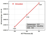
도 9는 스위칭 트랜지스터의 채널 폭에 따라서 누설전류가 달라지는 것을 나타내는 도면.
도 10은 스위칭 트랜지스터의 채널 도핑에 따라서 누설전류가 달라지는 것을 나타내는 도면.
도 11은 스위칭 트랜지스터의 활성층 두께에 따라서 누설전류가 달라지는 것을 나타내는 도면.
도 12는 스위칭 트랜지스터의 게이트 절연막 두께에 따라서 누설전류가 달라지는 것을 나타내는 도면.
도 13은 스위칭 트랜지스터의 실시 예를 나타내는 단면도.
도 14는 스위칭 트랜지스터의 LDD 도핑 농도에 따라서 누설전류가 달라지는 것을 나타내는 도면.
도 15는 스위칭 트랜지스터의 다른 실시 예를 나타내는 단면도.
도 16은 스위칭 트랜지스터의 광차단막 유무에 따라서 누설전류가 달라지는 것을 나타내는 도면.
도 17은 스위칭 트랜지스터의 또 다른 실시 예를 나타내는 단면도.
도 18은 듀얼 게이트 구조와 싱글 게이트 구조에서의 누설전류의 차이를 나타내는 도면.
도 19는 본 발명에 의한 스토리지 커패시터의 제1 실시 예를 나타내는 도면.
도 20은 본 발명에 의한 스토리지 커패시터의 제2 실시 예를 나타내는 도면.
도 21은 스토리지 커패시터의 용량에 따라서 누설전류가 달라지는 것을 나타내는 도면. 1 is a view showing an organic light emitting diode display device according to the present invention.
2 is a view showing an embodiment of a pixel included in an organic light emitting diode display according to the present invention.
3 is a timing diagram for driving an organic light emitting diode display according to the present invention.
4A and 4B are diagrams illustrating leakage currents of a low-temperature polysilicon transistor and an oxide semiconductor transistor, respectively;
5 is a diagram illustrating a change in luminance variation according to a frame rate;
Fig. 6 is a diagram showing a change in flicker according to a frame rate;
7 is a cross-sectional view illustrating structures of a driving transistor and a switching transistor according to an embodiment of the present invention.
8 is a cross-sectional view illustrating structures of a driving transistor and a switching transistor according to another embodiment;
9 is a diagram illustrating a change in leakage current according to a channel width of a switching transistor;
10 is a diagram illustrating a change in leakage current according to channel doping of a switching transistor;
11 is a diagram illustrating a change in leakage current according to the thickness of an active layer of a switching transistor;
12 is a diagram illustrating a change in leakage current according to a thickness of a gate insulating film of a switching transistor;
13 is a cross-sectional view showing an embodiment of a switching transistor;
14 is a diagram illustrating a change in leakage current according to an LDD doping concentration of a switching transistor;
15 is a cross-sectional view illustrating another embodiment of a switching transistor;
16 is a diagram illustrating a change in leakage current according to the presence or absence of a light blocking film of a switching transistor;
17 is a cross-sectional view illustrating another embodiment of a switching transistor;
18 is a diagram illustrating a difference in leakage current between a dual gate structure and a single gate structure;
19 is a view showing a first embodiment of a storage capacitor according to the present invention.
20 is a view showing a second embodiment of a storage capacitor according to the present invention.
21 is a diagram illustrating a change in leakage current according to the capacity of a storage capacitor;
이하 첨부된 도면을 참조하여 본 발명에 따른 바람직한 실시 예들을 상세히 설명한다. 명세서 전체에 걸쳐서 동일한 참조번호들은 실질적으로 동일한 구성요소들을 의미한다. 이하의 설명에서, 본 발명과 관련된 공지 기능 혹은 구성에 대한 구체적인 설명이 본 발명의 요지를 불필요하게 흐릴 수 있다고 판단되는 경우, 그 상세한 설명을 생략한다. Hereinafter, preferred embodiments according to the present invention will be described in detail with reference to the accompanying drawings. Like reference numerals refer to substantially identical elements throughout. In the following description, if it is determined that a detailed description of a known function or configuration related to the present invention may unnecessarily obscure the gist of the present invention, the detailed description thereof will be omitted.
도 1은 본 발명의 실시 예에 의한 유기발광다이오드 표시장치를 보여준다.1 shows an organic light emitting diode display according to an embodiment of the present invention.
도 1을 참조하면, 본 발명에 의한 유기발광다이오드 표시장치는 화소들(P)이 매트릭스 형태로 배열되는 표시패널(10), 데이터 구동회로(12), 게이트 구동회로(13) 및 타이밍 콘트롤러(11)를 구비한다. Referring to FIG. 1 , an organic light emitting diode display according to the present invention includes a
표시패널(10)은 복수 개의 화소(P)를 포함하고, 각각의 화소(P)들이 표시하는 계조를 기반으로 영상을 표시하기 위한 것이다. 화소(P)들은 수평라인들 각각에 복수 개가 일정한 간격으로 배열됨으로써 표시패널(10) 내에서 매트릭스 형태로 배치된다. The
이때, 각각의 화소(P)들은 서로 직교하는 데이터라인부(14)와 다수의 게이트라인부(15)가 교차되는 영역에 배치된다. 각 화소(P)에 접속하는 데이터라인부(14)는 초기화라인(14a) 및 데이터라인(14b)을 포함하고, 게이트라인부(15)는 제1 스캔라인(15a), 제2 스캔라인(15b) 및 에미션라인(15c)을 포함한다.In this case, each of the pixels P is disposed in a region where the
그리고 화소(P)들 각각은 유기발광다이오드(OLED), 구동트랜지스터(DT), 스위칭 트랜지스터(ST), 제1 및 제2 트랜지스터(T1,T2), 스토리지 커패시터(Cs) 및 보조커패시터(C1) 포함한다. In addition, each of the pixels P includes an organic light emitting diode (OLED), a driving transistor (DT), a switching transistor (ST), first and second transistors (T1 and T2), a storage capacitor (Cs), and an auxiliary capacitor (C1). include
타이밍 콘트롤러(11)는 데이터 구동회로(12) 및 게이트 구동회로(13)의 구동 타이밍을 제어하기 위한 것이다. 이를 위해서 타이밍 콘트롤러(11)는 외부로부터 입력되는 디지털 비디오 데이터(RGB)를 표시패널(10)의 해상도에 맞게 재정렬하여 데이터 구동회로(12)에 공급한다. 또한, 타이밍 콘트롤러(11)는 수직 동기신호(Vsync), 수평 동기신호(Hsync), 도트클럭신호(DCLK) 및 데이터 인에이블신호(DE) 등의 타이밍 신호들에 기초하여 데이터 구동회로(12)의 동작 타이밍을 제어하기 위한 데이터 제어신호(DDC)와, 게이트 구동회로(13)의 동작 타이밍을 제어하기 위한 게이트 제어신호(GDC)를 발생한다. The
데이터 구동회로(12)는 데이터라인부(14)를 구동하기 위한 것이다. 이를 위해서 데이터 구동회로(12)는 데이터 제어신호(DDC)를 기반으로 타이밍 콘트롤러(11)로부터 입력되는 디지털 비디오 데이터(RGB)를 아날로그 데이터전압으로 변환하여 데이터라인(14)들에 공급한다.The
게이트 구동회로(13)는 게이트라인부(15)를 구동하기 위한 것이다. 이를 위해서 게이트 구동회로(13)는 게이트 제어신호(GDC)를 기반으로 스캔신호, 발광제어신호, 및 초기화신호를 발생한다. 게이트 구동회로(13)는 스캔신호를 라인 순차 방식으로 스캔라인(15a)에 공급하고, 발광제어신호를 라인 순차 방식으로 에미션라인(15b)에 공급하며, 초기화신호를 라인 순차 방식으로 초기화라인(15c)에 공급한다. The
도 2는 도 1에 도시된 화소(P)의 일 예를 나타내는 것으로서, 수평라인의 화소(P)들 중의 하나를 도시한 것이다.FIG. 2 shows an example of the pixel P shown in FIG. 1 , and shows one of the pixels P on a horizontal line.
도 2를 참조하면, 본 발명의 일 실시 예에 따른 화소(P)는 유기발광다이오드(OLED), 구동트랜지스터(DT), 스위칭 트랜지스터(ST), 제1 및 제2 트랜지스터(T1,T2), 스토리지 커패시터(Cs) 및 보조 커패시터(C1)를 구비한다. Referring to FIG. 2 , a pixel P according to an embodiment of the present invention includes an organic light emitting diode (OLED), a driving transistor DT, a switching transistor ST, first and second transistors T1 and T2, A storage capacitor Cs and an auxiliary capacitor C1 are provided.
유기발광다이오드(OLED)는 구동트랜지스터(DT)로부터 공급되는 구동 전류에 의해 발광한다. 유기발광다이오드(OLED)의 애노드전극과 캐소드전극 사이에는 다층의 유기 화합물층이 형성된다. 유기 화합물층은 정공주입층(Hole Injection layer, HIL), 정공수송층(Hole transport layer, HTL), 발광층(Emission layer, EML), 전자수송층(Electron transport layer, ETL) 및 전자주입층(Electron Injection layer, EIL)을 포함한다. 유기발광다이오드(OLED)의 애노드전극은 구동트랜지스터(DT)의 소스전극에 접속되고, 캐소드전극은 저전압구동전압(EVSS)에 연결된다.The organic light emitting diode OLED emits light by a driving current supplied from the driving transistor DT. A multi-layered organic compound layer is formed between the anode electrode and the cathode electrode of the organic light emitting diode (OLED). The organic compound layer includes a hole injection layer (HIL), a hole transport layer (HTL), an emission layer (EML), an electron transport layer (ETL) and an electron injection layer (Electron Injection layer, EIL). The anode electrode of the organic light emitting diode OLED is connected to the source electrode of the driving transistor DT, and the cathode electrode is connected to the low voltage driving voltage EVSS.
구동트랜지스터(DT)는 자신의 게이트-소스 간의 전압으로 유기발광다이오드(OLED)에 인가되는 구동전류를 제어한다. 이를 위해서 구동트랜지스터(DT)의 게이트전극은 데이터전압(Vdata)의 입력단에 연결되고, 드레인전극은 구동전압(EVDD)의 입력단에 연결되며, 소스전극은 저전압구동전압(EVSS)과 연결된다.The driving transistor DT controls a driving current applied to the organic light emitting diode OLED by its gate-source voltage. To this end, the gate electrode of the driving transistor DT is connected to the input terminal of the data voltage Vdata, the drain electrode is connected to the input terminal of the driving voltage EVDD, and the source electrode is connected to the low voltage driving voltage EVSS.
제1 트랜지스터(T1)는 발광제어신호(EM)에 응답하여, 구동전압(EVDD) 입력단과 구동트랜지스터(DT) 간의 전류 경로를 제어한다. 이를 위해서 제1 트랜지스터(T1)의 게이트 전극은 발광제어신호라인(15c)에, 드레인전극은 구동전압(EVDD) 입력단에, 소스전극은 구동트랜지스터(DT)에 연결된다. The first transistor T1 controls a current path between the driving voltage EVDD input terminal and the driving transistor DT in response to the emission control signal EM. To this end, the gate electrode of the first transistor T1 is connected to the emission
제2 트랜지스터(T2)는 제(n-1) 수평라인의 스캔신호인 제2 스캔신호(Scan2)에 응답하여, 초기화라인(14a)으로부터 제공받는 초기화전압(Vini)을 제2 노드(n2)로 제공한다. 이를 위해서 제2 트랜지스터(T2)의 게이트 전극은 제(n-1) 스캔라인(15a)에, 드레인전극은 초기화라인(14a)에 소스전극은 제2 노드(n2)에 연결된다. The second transistor T2 applies the initialization voltage Vini received from the
구동트랜지스터(DT)와 제1 및 제2 트랜지스터(T1,T2)는 저온 폴리 실리콘(Low Temperature Poly-Silicon:LTPS)을 이용한 트랜지스터로 형성된다. 저온 폴리 실리콘 트랜지스터는 전자 이동도가 높고 신뢰성이 우수하여 고성능의 표시장치를 구현할 수 있다. The driving transistor DT and the first and second transistors T1 and T2 are formed of transistors using low temperature poly-silicon (LTPS). The low-temperature polysilicon transistor has high electron mobility and excellent reliability, so that a high-performance display device can be realized.
스위칭 트랜지스터(ST)는 제n 수평라인의 스캔신호인 제1 스캔신호(Scan1)에 응답하여, 데이터라인(14b)으로부터 제공받는 기준전압(Vref) 또는 데이터전압(Vdata)을 구동트랜지스터(DT)에 제공한다. 이를 위해서, 스위칭 트랜지스터(ST)의 게이트 전극은 제1 스캔라인(Scan1)에, 드레인전극은 데이터라인(14b)에, 소스전극은 구동트랜지스터(DT)에 연결된다.The switching transistor ST receives the reference voltage Vref or the data voltage Vdata provided from the
스위칭 트랜지스터(ST)는 산화아연(Zinc Oxide:ZnO) 또는 갈륨-인듐-징크-옥사이드(GaInZnO;GIZO)와 같은 산화물 반도체를 활성층으로 이용한 산화물 트랜지스터로 형성된다. 산화물 트랜지스터는 누설전류(Off-Current)가 낮기 때문에, 산화물 트랜지스터를 이용한 스위칭 트랜지스터(ST)는 누설전류로 인해서 구동트랜지스터(DT)의 게이트-소스 전위가 감소하는 것을 방지할 수 있다. 따라서 저주파 구동을 할 때에도, 누설전류로 인해서 구동트랜지스터(DT)의 게이트-소스 전위가 감소하여, 이로 인하여 플리커(flicker)가 발생하는 것을 방지할 수 있다. 이에 대한 자세한 설명은 후술하기로 한다. The switching transistor ST is formed of an oxide transistor using an oxide semiconductor such as zinc oxide (ZnO) or gallium-indium-zinc-oxide (GaInZnO; GIZO) as an active layer. Since the oxide transistor has a low leakage current (Off-Current), the switching transistor ST using the oxide transistor can prevent a decrease in the gate-source potential of the driving transistor DT due to the leakage current. Accordingly, even during low-frequency driving, the gate-source potential of the driving transistor DT decreases due to the leakage current, thereby preventing flicker from occurring. A detailed description thereof will be provided later.
스토리지 커패시터(Cs)는 데이터라인(14b)으로부터 제공받는 데이터전압(Vdata)을 한 프레임동안 유지하여 구동트랜지스터(DT)가 일정한 전압을 유지하도록 한다. 이를 위해서 스토리지 커패시터(Cs)는 구동트랜지스터(DT)의 게이트 전극과 소스 전극에 연결된다. 보조커패시터(C1)는 제2 노드(n2)에서 스토리지 커패시터(Cs)와 직렬로 연결되어, 구동전압(Vdata)의 효율을 높여준다.The storage capacitor Cs maintains the data voltage Vdata received from the
상술한 바와 같은 구조를 갖는 화소(P)의 동작을 살펴보면 다음과 같다. 도 3은 도 2의 화소(P)에 인가되는 신호들(EM,SCAN,INIT,DATA)과, 그에 따른 구동트랜지스터(DT)의 게이트전극과 소스전극의 전위변화를 나타내는 파형도이다. The operation of the pixel P having the above-described structure will be described below. FIG. 3 is a waveform diagram illustrating signals EM, SCAN, INIT, and DATA applied to the pixel P of FIG. 2 and potential changes of the gate electrode and the source electrode of the driving transistor DT accordingly.
도 3을 참조하면, 본 발명에 따른 화소(P)의 동작은 구동트랜지스터(DT)의 게이트-소스 전위를 특정 전압으로 초기화하는 초기화기간(Ti), 구동트랜지스터(DT)의 문턱전압을 검출 및 저장하는 샘플링기간(Ts), 데이터전압(Vdata)을 인가하는 라이팅 기간(Tw), 문턱전압과 데이터전압(Vdata)을 이용하여 유기발광다이오드(OLED)에 인가되는 구동 전류를 문턱전압과 무관하게 보상하여 발광하는 발광기간(Te)을 포함한다. Referring to FIG. 3 , the operation of the pixel P according to the present invention includes an initialization period Ti in which the gate-source potential of the driving transistor DT is initialized to a specific voltage, and the threshold voltage of the driving transistor DT is detected and The sampling period (Ts) for storing, the writing period (Tw) for applying the data voltage (Vdata), and the driving current applied to the organic light emitting diode (OLED) using the threshold voltage and the data voltage (Vdata) are irrespective of the threshold voltage. It includes a light emission period Te for compensating for light emission.
초기화기간(Ti) 동안에 제2 트랜지스터(T2)는 제2 스캔신호(Scan2)에 응답하여 초기화라인(14a)으로부터 제공받는 초기화전압(Vini)을 제2 노드(n2)에 공급한다. 따라서, 제2 노드(n2)의 전압인 구동트랜지스터(DT)의 소스전압(Vs)은 초기화전압(Vini)의 전위를 갖는다. 그리고 스위칭 트랜지스터(ST)는 제1 스캔신호(Scan1)에 응답하여 데이터라인(14b)으로부터 제공받는 기준전압(Vref)을 구동트랜지스터(DT)의 게이트전극의 제1 노드(n1)에 공급한다. 따라서, 제1 노드(n1)의 전압인 구동트랜지스터(DT)의 게이트전압(Vg)은 기준전압(Vref)의 전위를 갖는다. During the initialization period Ti, the second transistor T2 supplies the initialization voltage Vini received from the
초기화기간(Ti)에서 제2 노드(n2)에 공급되는 초기화전압(Vini)은 화소(P)를 일정 수준으로 초기화하기 위한 것으로서, 이때 초기화전압(Vini)의 크기는 유기발광다이오드(OLED)가 발광하지 않도록 유기발광다이오드(OLED)의 동작전압 보다 작은 전압값으로 설정된다. 예컨대, 초기화전압(Vini)은 -1 내지 +1(V)의 크기를 갖는 전압으로 설정할 수 있다.The initialization voltage Vini supplied to the second node n2 in the initialization period Ti is to initialize the pixel P to a certain level, and in this case, the magnitude of the initialization voltage Vini is determined by the organic light emitting diode OLED. It is set to a voltage value smaller than the operating voltage of the organic light emitting diode (OLED) so as not to emit light. For example, the initialization voltage Vini may be set to a voltage having a magnitude of -1 to +1 (V).
샘플링기간(Ts) 동안에, 스위칭 트랜지스터(ST)는 제1 스캔신호(Scan1)에 응답하여 데이터라인(14b)으로부터 제공받는 기준전압(Vref)을 제1 노드(n1)로 공급한다. 그리고 제1 트랜지스터(T1)는 발광제어신호(EM)에 응답하여 구동전압(EVDD)을 구동트랜지스터(DT)로 공급한다. 이때, 구동트랜지스터 게이트전극전압(Vg)은 기준전압(Vref)를 유지한다. 그리고 제2 노드(n2)가 플로팅(floating) 상태임에 따라서, 제2 노드(n2)의 전압은 구동전압(EVDD)에서 제1 트랜지스터(T1)와 구동트랜지스터(DT)를 통해 흐르는 전류가 축적된다. 샘플링기간(Ts)을 통해서 상승한 전압은 기준전압(Vref)과 구동트랜지스터(DT)의 문턱전압(Vth) 간의 차이에 해당하는 크기를 갖는 전압으로 포화(saturation)된다. 즉, 샘플링 기간(Ts)을 통해서, 구동트랜지스터(DT)의 게이트-소스 간의 전위차는 문턱전압(Vth)의 크기가 된다. During the sampling period Ts, the switching transistor ST supplies the reference voltage Vref received from the
라이팅 기간(Tw) 동안에 제1 및 제2 트랜지스터(T1,T2)는 턴-오프 된다. 그리고 스위칭 트랜지스터(ST)는 턴-온 되면서 데이터라인(14b)으로부터 제공받는 데이터전압(Vdata)을 제1 노드(n1)로 공급한다. 이때, 플로팅(floating) 상태인 제2 노드(n2) 전압은 스토리지 커패시터(Cs) 및 보조커패시터(C1)의 비율에 의해서 커플링(Coupling)되어서 상승하거나 하강한다.During the writing period Tw, the first and second transistors T1 and T2 are turned off. In addition, the switching transistor ST is turned on and supplies the data voltage Vdata received from the
발광기간(Te) 동안에 제2 및 스위칭 트랜지스터(T2,ST)는 턴-오프되며, 제1 트랜지스터(T1)는 턴-온된다. 발광기간 동안에 스토리지 커패시터(Cs)에 저장된 데이터전압(Vdata)은 유기발광다이오드(OLED)로 공급되고, 이에 따라서 유기발광다이오드(OLED)는 데이터전압(Vdata)에 비례하는 밝기로 발광한다. 이때, 라이팅 기간(Tw)에서 결정된 제1 노드(n1) 및 제2 노드(2)의 전압에 의해서 구동트랜지스터(DT)에 전류가 흐르게 되어 유기발광다이오드(OLED)로 원하는 전류가 공급되고, 이에 따라서 유기발광다이오드(OLED)는 데이터전압(Vdata)에 의해 밝기를 조절할 수 있다.During the light emission period Te, the second and switching transistors T2 and ST are turned off, and the first transistor T1 is turned on. During the light emission period, the data voltage Vdata stored in the storage capacitor Cs is supplied to the organic light emitting diode OLED, and accordingly, the organic light emitting diode OLED emits light with a brightness proportional to the data voltage Vdata. At this time, a current flows in the driving transistor DT by the voltages of the first node n1 and the
유기발광다이오드(OLED)의 발광 과정에서, 스위칭 트랜지스터(ST)는 누설전류가 적은 산화물 반도체 트랜지스터로 형성되기 때문에 스토리지 커패시터(Cs)의 전압강하를 억제할 수 있다.In the light emitting process of the organic light emitting diode (OLED), since the switching transistor ST is formed of an oxide semiconductor transistor having a small leakage current, a voltage drop of the storage capacitor Cs can be suppressed.
스위칭 트랜지스터(ST)의 누설전류는 스위칭 트랜지스터(ST)의 게이트-소스 전위가 문턱전압(Vth) 미만이어서 스위칭 트랜지스터(ST)가 턴-오프 된 상태일 때, 드레인 전극에서 소스 전극으로 흐르는 전류이다. 스위칭 트랜지스터(ST)의 누설전류는 스토리지 커패시터(Cs)의 전압강하를 야기한다. 스토리지 커패시터(Cs)의 전압강하는 구동트랜지스터(DT)의 게이트-소스 전위 변화(△Vgs)를 야기한다. 구동트랜지스터(DT)의 게이트-소스 전위는 유기발광다이오드(OLED)의 발광 휘도를 결정하기 때문에, 스토리지 커패시터(Cs)의 전압강하는 유기발광다이오드(OLED)의 휘도 저하를 초래한다. 즉, 스위칭 트랜지스터(ST)의 누설전류는 유기발광다이오드(OLED)의 휘도 저하를 초래한다. 하나의 프레임 기간 동안 휘도 저하가 발생하면 이어지는 프레임의 초기 휘도와의 차이로 인해서, 프레임이 변경되는 순간 플리커(flicker) 현상이 발생한다. The leakage current of the switching transistor ST is a current flowing from the drain electrode to the source electrode when the switching transistor ST is turned off because the gate-source potential of the switching transistor ST is less than the threshold voltage Vth. . The leakage current of the switching transistor ST causes a voltage drop of the storage capacitor Cs. The voltage drop of the storage capacitor Cs causes a gate-source potential change ΔVgs of the driving transistor DT. Since the gate-source potential of the driving transistor DT determines the emission luminance of the organic light emitting diode OLED, the voltage drop of the storage capacitor Cs causes a decrease in the luminance of the organic light emitting diode OLED. That is, the leakage current of the switching transistor ST causes a decrease in luminance of the organic light emitting diode OLED. When luminance is lowered during one frame period, a flicker phenomenon occurs at the moment the frame is changed due to a difference from the initial luminance of subsequent frames.
도 4의 (a)는 게이트-소스 전위에 따라서 저온 폴리 실리콘 트랜지스터의 누설전류를 나타내는 도면이고, 도 4의 (b)는 게이트-소스 전위에 따라서 산화물 반도체 트랜지스터의 누설전류를 나타내는 도면이다. 산화물 반도체 트랜지스터의 누설전류는 저온 폴리 실리콘 트랜지스터의 누설전류에 비해 매우 작으며 측정 장비의 측정 범위 이하에서 정확히 측정되지 않을 정도이다. 도 4의 (b)에서 보는 것처럼, 실시 예의 스위칭 트랜지스터(ST)는 산화물 반도체를 사용하여 누설전류가 무시할 수 있을 정도로 매우 작다. 따라서, 본 발명의 유기발광다이오드 표시장치는 누설전류로 인한 플리커 현상을 억제할 수 있다. 4A is a diagram illustrating the leakage current of a low-temperature polysilicon transistor according to a gate-source potential, and FIG. 4B is a diagram illustrating a leakage current of an oxide semiconductor transistor according to a gate-source potential. The leakage current of the oxide semiconductor transistor is very small compared to the leakage current of the low-temperature polysilicon transistor, and it is not accurately measured below the measurement range of the measuring equipment. As shown in FIG. 4B , the switching transistor ST of the embodiment uses an oxide semiconductor so that leakage current is negligibly small. Accordingly, the organic light emitting diode display device of the present invention can suppress the flicker phenomenon due to leakage current.
이에 따라서, 본 발명의 유기발광다이오드 표시장치는 저주파 구동시에도 플리커 현상이 발생하지 않는 표시장치를 제공한다. 도 5는 주파수에 따라서 프레임 간의 휘도 변화를 나타내는 도면이다. 도 5에서와 같이, 저주파 구동의 발광기간(Te2)은 표준 주파수 구동의 발광기간(Te1) 보다 길게 된다. 따라서 저주파 구동에서의 휘도변화량(△L)은 표준 주파수 구동에서의 휘도변화량(△L') 보다 크기 때문에, 저주파 구동시에는 플리커 문제점이 크게 두드러진다. Accordingly, the organic light emitting diode display device of the present invention provides a display device in which the flicker phenomenon does not occur even when driving at a low frequency. 5 is a diagram illustrating a change in luminance between frames according to frequency. As shown in FIG. 5 , the light emission period Te2 of the low frequency driving is longer than the light emission period Te1 of the standard frequency driving. Therefore, since the luminance change amount ΔL in the low frequency driving is larger than the luminance change amount ΔL′ in the standard frequency driving, the flicker problem is greatly conspicuous during the low frequency driving.
본 발명은 스위칭 트랜지스터의 누설전류가 매우 작아서 스토리지 커패시터(Cs)의 전압강하가 매우 작기 때문에, 저주파 구동시에도 플리커 현상이 발생하지 않는다. In the present invention, since the leakage current of the switching transistor is very small and the voltage drop of the storage capacitor Cs is very small, the flicker phenomenon does not occur even when driving at a low frequency.
도 6의 (a)는 구동 주파수 즉, 프레임 레이트에 따라서 플리커의 변화를 나타내는 도면이고, 도 6의 (b)는 구동 주파수에 따라서 사람의 시각적 민감도를 나타내는 도면이다. 도 6의 (c)는 도 6의 (a) 및 (b)를 적분한 결과에 따라서 구동 주파수에 따라서 사람이 느끼는 플리커의 변화를 나타내는 도면이다. FIG. 6A is a diagram illustrating a change in flicker according to a driving frequency, that is, a frame rate, and FIG. 6B is a diagram illustrating a human visual sensitivity according to a driving frequency. FIG. 6(c) is a diagram illustrating a change in flicker perceived by a person according to a driving frequency according to the result of integrating FIGS. 6(a) and (b).
도 6의 (a) 및 (c)에서 제1 그래프(①)는 스위칭 트랜지스터가 저온 폴리 실리콘으로 형성된 표시장치에서의 플리커 변화를 나타내고, 제2 그래프(②)는 스위칭 트랜지스터가 산화물 반도체 트랜지스터로 형성되는 본 발명의 표시장치에서의 플리커 변화를 나타낸다. 도 6의 (a)에서와 같이, 스위칭 트랜지스터가 저온 폴리 실리콘으로 형성된 표시장치는 구동주파수가 30Hz 이하일 경우에 구동주파수가 낮아질수록 플리커가 급증한다. 반면에, 스위칭 트랜지스터(ST)가 산화물 반도체 트랜지스터로 형성된 표시장치는 구동주파수가 낮아질수록 플리커가 감소한다. 플리커의 차이는 40Hz 이하에서 차이가 나기 시작하여, 20Hz 이하에서 그 차이가 커지기 시작하고, 10Hz 이하에서 더욱 커진다. 결국, 스위칭 트랜지스터를 저온 폴리 실리콘으로 형성하는 표시장치는 30Hz 이하의 구동주파수를 갖는 표시장치에 적용할 경우에 플리커 문제점이 발생하지만, 본 발명과 같이 스위칭 트랜지스터(ST)가 산화물 반도체 트랜지스터로 형성된 표시장치는 정지영상에 가까운 저주파 구동을 수행하여도 플리커가 거의 발생하지 않는다. 6A and 6C, the first graph (①) shows the flicker change in the display device in which the switching transistor is formed of low-temperature polysilicon, and the second graph (②) shows the switching transistor is formed of an oxide semiconductor transistor. shows the flicker change in the display device of the present invention. As shown in (a) of FIG. 6 , in the display device in which the switching transistor is formed of low-temperature polysilicon, when the driving frequency is 30 Hz or less, the flicker increases as the driving frequency decreases. On the other hand, in the display device in which the switching transistor ST is formed of an oxide semiconductor transistor, the flicker decreases as the driving frequency decreases. The difference in flicker starts to appear at 40 Hz or less, the difference starts to increase at 20 Hz or less, and becomes even larger at 10 Hz or less. As a result, the display device in which the switching transistor is formed of low-temperature polysilicon has a flicker problem when applied to a display device having a driving frequency of 30 Hz or less. Even if the device performs low-frequency driving close to a still image, almost no flicker occurs.
또한 사람의 시각적 민감도는 도 6의 (b)에서와 같이 10Hz에서 시각적 감각이 가장 민감하기 때문에, 10Hz이하일 경우에 본 발명의 유기발광다이오드 표시장치에서 플리커가 급격히 감소하는 것을 알 수 있다. In addition, since human visual sensitivity is most sensitive at 10 Hz as shown in FIG. 6(b) , it can be seen that flicker is rapidly reduced in the organic light emitting diode display device of the present invention when it is 10 Hz or less.
도 6의 (a)에 도시된 주파수에 따른 플리커의 발생은 온도에 따라서 달라질 수 있다. 예컨대, 상온에서는 도 6의 (a)에서와 같이 30Hz이하의 주파수에서부터 본 발명의 효과를 기대할 수 있지만, 고온에서는 저온 폴리 실리콘만을 이용한 표시장치와 스위칭 트랜지스터를 산화물 트랜지스터로 적용한 표시장치 간의 플리커 변화가 더 높은 주파수에서부터 차이가 발생한다. 예컨대, 고온에서는 60Hz 이하의 주파수에서부터 본 발명을 적용한 표시장치가 저온 폴리 실리콘만을 이용한 표시장치에 대비하여 플리커 레벨이 감소한다.The occurrence of flicker according to the frequency shown in (a) of FIG. 6 may vary depending on the temperature. For example, at room temperature, the effect of the present invention can be expected from a frequency of 30 Hz or less as in FIG. The difference occurs at higher frequencies. For example, at a high temperature, the flicker level of the display device to which the present invention is applied from a frequency of 60 Hz or less is reduced compared to a display device using only low-temperature polysilicon.
이처럼 본 발명은 프레임 레이트가 낮은 주파수에서도 플리커가 발생하지 않기 때문에, 소비전력을 줄이기 위해서 낮은 구동주파수를 이용하는 표시장치에 적용될 수 있다. 특히, 본 발명은 휴대용 표시장치에서 소비전력을 줄이기 위해서 구동주파수를 크게 줄여도 무방한 경우에 적용될 수 있다. 일례로 휴대용 전자시계는 초 단위로 표시화면을 변경할 경우에 1Hz의 구동주파수를 이용할 수 있고, 본 발명은 1Hz 또는 정지영상에 가까운 구동주파수를 이용하여도 플리커가 거의 발생하지 않는다. 또한, 본 발명은 휴대단말기의 대기화면에서와 같은 정지영상을 표시할 경우에도 구동주파수를 크게 낮출 수 있어서 소비전력을 대폭 감소시킬 수 있다. As described above, the present invention can be applied to a display device using a low driving frequency in order to reduce power consumption because flicker does not occur even at a frequency having a low frame rate. In particular, the present invention can be applied to a case in which a driving frequency may be greatly reduced in order to reduce power consumption in a portable display device. For example, a portable electronic watch can use a driving frequency of 1 Hz when changing a display screen in seconds, and in the present invention, flicker hardly occurs even when a driving frequency close to 1 Hz or a still image is used. In addition, according to the present invention, even when a still image is displayed, such as on a standby screen of a portable terminal, the driving frequency can be significantly lowered, thereby significantly reducing power consumption.
또한 본 발명은 전자책(E-Book)과 같이 동영상 수준의 높은 구동주파수를 필요로 하지 않는 단말기에도 적용되어 소비전력을 크게 줄임으로써, 휴대 단말기의 휴대성을 높일 수 있다. In addition, the present invention is applied to a terminal that does not require a high driving frequency of a moving picture, such as an e-book, and greatly reduces power consumption, thereby increasing the portability of the portable terminal.
도 7은 구동트랜지스터(DT) 및 스위칭 트랜지스터(ST)의 실시 예를 나타내는 단면도이다. 도 7을 참조하여 구동트랜지스터(DT) 및 스위칭 트랜지스터(ST)의 구조 및 형성방법을 살펴보면 다음과 같다. 7 is a cross-sectional view illustrating an embodiment of the driving transistor DT and the switching transistor ST. The structure and formation method of the driving transistor DT and the switching transistor ST will be described with reference to FIG. 7 .
구동트랜지스터(DT)의 형성과정은 기판(substrate)에 버퍼층(buffer)을 형성하는 단계를 포함한다. 버퍼층(buffer)은 산화막(SiO2)을 이용할 수 있다. 버퍼층(buffer) 상에는 구동트랜지스터(DT) 활성층으로 이용되는 저온 폴리 실리콘층(p-Si)이 형성된다. 저온 폴리 실리콘층(p-Si)은 이온 주입 공정을 통해서 일부 영역이 소스, 드레인 영역(S,D)으로 구현된다. 저온 폴리 실리콘층(p-Si) 상에는 게이트 절연막(GI)이 형성되며, 게이트 절연막(GI) 상에는 제1 게이트층(GATE1)이 형성된다. 게이트 절연막(GI)은 산화막(SiO2)으로 형성될 수 있다. 이어서, 제1 내지 제3 절연막(ILD1~ILD3)이 제1 게이트층(GATE1)을 덮도록 순차적으로 형성된다. 또한, 제3 절연막(ILD3) 상에는 보호층(PAS)이 형성된다.The process of forming the driving transistor DT includes forming a buffer layer on a substrate. An oxide layer (SiO2) may be used as the buffer layer. A low-temperature polysilicon layer (p-Si) used as an active layer of the driving transistor DT is formed on the buffer layer. A portion of the low-temperature polysilicon layer (p-Si) is implemented as source and drain regions S and D through an ion implantation process. A gate insulating layer GI is formed on the low-temperature polysilicon layer p-Si, and a first gate layer GATE1 is formed on the gate insulating layer GI. The gate insulating layer GI may be formed of an oxide layer SiO2. Subsequently, first to third insulating layers ILD1 to ILD3 are sequentially formed to cover the first gate layer GATE1 . In addition, a passivation layer PAS is formed on the third insulating layer ILD3 .
스위칭 트랜지스터(ST)의 형성과정은 기판(substrate)에 버퍼층(buffer)을 형성하는 단계를 포함한다. 게이트 절연막(GI)에는 제2 게이트층(GATE2)이 형성된다. 제3 절연막(ILD3)은 제2 게이트층(GATE2)을 덮도록 형성된다. 제3 절연막(ILD3) 상에는 산화물 반도체층(Active)이 형성된다. 산화물 반도체층(Active)의 일부 영역에는 소스, 드레인 전극(S,D)이 형성되고, 소스 전극(S)과 드레인 전극(D)을 덮도록 보호층(PAS)이 형성된다. The process of forming the switching transistor ST includes forming a buffer layer on a substrate. A second gate layer GATE2 is formed on the gate insulating layer GI. The third insulating layer ILD3 is formed to cover the second gate layer GATE2 . An oxide semiconductor layer Active is formed on the third insulating layer ILD3 . Source and drain electrodes S and D are formed in some regions of the oxide semiconductor layer Active, and a protective layer PAS is formed to cover the source electrode S and the drain electrode D.
도 8은 다른 실시 예에 의한 유기발광다이오드 표시장치의 구동트랜지스터(DT) 및 스위칭 트랜지스터(ST)의 단면도이다. 이 실시 예에서 전술한 실시 예와 동일한 구성에 대해서는 동일한 도면부호를 사용하고 자세한 설명을 생략하기로 한다. 8 is a cross-sectional view of a driving transistor DT and a switching transistor ST of an organic light emitting diode display according to another exemplary embodiment. In this embodiment, the same reference numerals are used for the same components as those of the above-described embodiment, and detailed descriptions thereof will be omitted.
도 8을 참조하면, 다른 실시 예에 의한 유기발광다이오드 표시장치는 구동트랜지스터 및 스위칭 트랜지스터(ST)를 모두 저온 폴리 실리콘 트랜지스터를 이용한다. Referring to FIG. 8 , in the organic light emitting diode display according to another embodiment, both the driving transistor and the switching transistor ST use low-temperature polysilicon transistors.
스위칭 트랜지스터 채널 폭(W2)은 구동트랜지스터 채널 폭(W1)에 대비하여 5~15% 좁게 형성된다. 도 9에서와 같이, 스위칭 트랜지스터(ST) 및 구동트랜지스터(DT)의 누설전류는 스위칭 트랜지스터(ST)의 채널 폭에 비례한다. 따라서, 본 발명은 스위칭 트랜지스터 채널 폭(W2)을 구동트랜지스터 채널 폭(W1)에 대비하여 좁게 형성하여, 스위칭 트랜지스터(ST)의 누설전류를 감소시킬 수 있다. 스위칭 트랜지스터 채널 폭(W2)을 줄일수록 누설전류는 감소하지만, 구동의 신뢰성 등에 영향을 끼치지 않도록 스위칭 트랜지스터 채널 폭(W2)은 구동트랜지스터 채널 폭(W1) 보다 5~15% 좁게 설정될 수 있다. The switching transistor channel width W2 is formed to be 5 to 15% narrower than the driving transistor channel width W1. As shown in FIG. 9 , leakage currents of the switching transistor ST and the driving transistor DT are proportional to the channel width of the switching transistor ST. Accordingly, according to the present invention, the leakage current of the switching transistor ST can be reduced by forming the switching transistor channel width W2 to be narrower than the driving transistor channel width W1 . As the switching transistor channel width W2 is reduced, the leakage current decreases, but the switching transistor channel width W2 may be set to be 5 to 15% narrower than the driving transistor channel width W1 so as not to affect the reliability of driving. .
스위칭 트랜지스터(ST)의 활성층(p-Si)의 도핑 농도는 구동트랜지스터(DT)의 활성층(p-Si) 도핑 농도 보다 5~15% 높게 형성된다. 도 10에서와 같이, 스위칭 트랜지스터(ST) 및 구동트랜지스터(DT)의 누설전류는 스위칭 트랜지스터(ST)의 도핑 농도에 반비례한다. 이는 활성층(p-Si)의 도핑 농도가 증가하면 LDD(Lightly Doped Drain)와의 PN 접합부위의 저항이 증가하여 누설전류가 감소하기 때문이다. 따라서, 본 발명은 스위칭 트랜지스터(ST) 활성층(p-Si)의 도핑 농도를 구동트랜지스터(DT) 활성층(p-Si)의 도핑 농도보다 높게 형성하여 스위칭 트랜지스터(ST)의 누설전류를 감소시킬 수 있다. 스위칭 트랜지스터(ST)의 도핑 농도를 높일수록 누설전류는 감소하지만, 구동의 신뢰성 등에 영향을 끼치지 않도록 스위칭 트랜지스터(ST) 활성층(p-Si)의 도핑 농도는 구동트랜지스터 활성층(p-Si) 도핑 농도의 5~15% 높게 형성될 수 있다.The doping concentration of the active layer p-Si of the switching transistor ST is 5 to 15% higher than the doping concentration of the active layer p-Si of the driving transistor DT. As shown in FIG. 10 , leakage currents of the switching transistor ST and the driving transistor DT are inversely proportional to the doping concentration of the switching transistor ST. This is because, when the doping concentration of the active layer (p-Si) increases, the resistance of the PN junction with the Lightly Doped Drain (LDD) increases and the leakage current decreases. Accordingly, the present invention can reduce the leakage current of the switching transistor ST by forming the doping concentration of the active layer p-Si of the switching transistor ST to be higher than the doping concentration of the active layer p-Si of the driving transistor DT. have. As the doping concentration of the switching transistor ST is increased, the leakage current is decreased, but the doping concentration of the active layer p-Si of the switching transistor ST is not affected such as driving reliability. It can be formed as high as 5-15% of the concentration.
스위칭 트랜지스터(ST)의 활성층 두께(d2)는 구동트랜지스터(DT) 활성층 두께(d1)보다 5~15% 얇은 두께로 형성된다. 도 11에서와 같이, 스위칭 트랜지스터(ST) 및 구동트랜지스터()의 누설전류는 활성층 두께(d2)에 비례한다. 따라서, 본 발명은 스위칭 트랜지스터(ST)의 활성층 두께(d2)를 구동트랜지스터 활성층 두께(d1)보다 얇게 형성하여 누설전류를 줄일 수 있다. 스위칭 트랜지스터(ST)의 활성층 두께(d2)를 줄일수록 누설전류는 감소하지만, 구동의 신뢰성 등에 영향을 끼치지 않도록 스위칭 트랜지스터(ST)의 활성층 두께(d2)는 구동트랜지스터(DT)의 활성층 두께(d1)보다 5~15% 얇은 두께로 형성될 수 있다. The active layer thickness d2 of the switching transistor ST is formed to be 5 to 15% thinner than the active layer thickness d1 of the driving transistor DT. As shown in FIG. 11 , leakage currents of the switching transistor ST and the driving transistor d are proportional to the thickness d2 of the active layer. Accordingly, according to the present invention, the leakage current can be reduced by forming the active layer thickness d2 of the switching transistor ST to be thinner than the driving transistor active layer thickness d1. As the thickness d2 of the active layer of the switching transistor ST is reduced, the leakage current decreases, but the active layer thickness d2 of the switching transistor ST is the thickness of the active layer of the driving transistor DT ( It may be formed to a
스위칭 트랜지스터(ST)의 게이트 절연막(GI) 두께(h2)는 구동트랜지스터(DT) 게이트 절연막(GI) 두께(h1)보다 5~15% 두꺼운 두께로 형성된다. 도 12에서와 같이, 스위칭 트랜지스터(ST) 및 구동트랜지스터(DT)의 누설전류는 게이트 절연막(GI) 두께(d2)에 반비례한다. 따라서, 본 발명은 스위칭 트랜지스터(ST)의 게이트 절연막(GI) 두께(d2)를 구동트랜지스터(DT) 게이트 절연막(GI) 두께보다 두껍게 형성하여 누설전류를 줄일 수 있다. 스위칭 트랜지스터(ST)의 게이트 절연막(GI) 두께(d2)를 두껍게 할수록 누설전류는 감소하지만, 구동의 신뢰성 등에 영향을 끼치지 않도록 스위칭 트랜지스터(ST)의 게이트 절연막(GI) 두께(d2)는 구동트랜지스터(DT)의 게이트 절연막(GI) 두께(d1)보다 5~15% 두꺼운 두께로 형성될 수 있다. The thickness h2 of the gate insulating layer GI of the switching transistor ST is 5 to 15% thicker than the thickness h1 of the gate insulating layer GI of the driving transistor DT. As shown in FIG. 12 , leakage currents of the switching transistor ST and the driving transistor DT are inversely proportional to the thickness d2 of the gate insulating layer GI. Accordingly, according to the present invention, the thickness d2 of the gate insulating layer GI of the switching transistor ST is formed to be thicker than the thickness of the gate insulating layer GI of the driving transistor DT to reduce leakage current. As the thickness d2 of the gate insulating layer GI of the switching transistor ST increases, the leakage current decreases. However, the thickness d2 of the gate insulating layer GI of the switching transistor ST is increased so as not to affect the reliability of driving. The gate insulating layer GI of the transistor DT may be formed to have a
도 13, 도 15 및 도 17은 각각 저온 폴리 실리콘을 이용하는 스위칭 트랜지스터(ST)의 변형 예들을 나타내고 있다. 13, 15, and 17 show modified examples of the switching transistor ST using low-temperature polysilicon, respectively.
도 13을 참조하면, 본 발명의 스위칭 트랜지스터(ST)는 낮은 도핑 드레인 영역(Lightly Doped Drain; 이하, LDD)의 도핑 농도가 구동트랜지스터(DT)의 LDD의 도핑 농도보다 5~15% 낮게 형성될 수 있다. 도 14에서와 같이, 스위칭 트랜지스터(ST) 및 구동트랜지스터(DT)의 누설전류는 LDD의 도핑 농도에 비례한다. 이는 LDD의 도핑 농도가 증가하면 활성층과의 접합부에서 저항이 줄어들어서 누설전류도 증가하기 때문이다. 따라서, 본 발명은 스위칭 트랜지스터(ST)의 LDD 도핑 농도를 구동트랜지스터(DT)의 도핑 농도보다 낮게 형성하여 누설전류를 줄일 수 있다. 스위칭 트랜지스터(ST)의 LDD 도핑 농도를 낮게 할수록 누설전류는 감소하지만, 구동의 신뢰성 등에 영향을 끼치지 않도록 스위칭 트랜지스터(ST)의 LDD 도핑 농도는 구동트랜지스터(DT)의 LDD 도핑 농도보다 5~15% 낮게 형성될 수 있다.Referring to FIG. 13 , in the switching transistor ST of the present invention, the doping concentration of the lightly doped drain region (hereinafter, LDD) is 5 to 15% lower than the doping concentration of the LDD of the driving transistor DT. can As shown in FIG. 14 , the leakage currents of the switching transistor ST and the driving transistor DT are proportional to the doping concentration of the LDD. This is because, when the doping concentration of the LDD increases, the resistance at the junction with the active layer decreases and the leakage current also increases. Accordingly, according to the present invention, the LDD doping concentration of the switching transistor ST is lower than the doping concentration of the driving transistor DT, thereby reducing the leakage current. Leakage current decreases as the LDD doping concentration of the switching transistor ST is lowered, but the LDD doping concentration of the switching transistor ST is 5 to 15 higher than the LDD doping concentration of the driving transistor DT so as not to affect the reliability of driving. % can be formed.
도 15를 참조하면, 스위칭 트랜지스터(ST)는 광 차단층(Bottom Shield Metal;BSM)을 더 포함한다. 광 차단층(BSM)은 버퍼층(Buffer)을 사이에 두고 채널층(Channel)의 하부 영역에서 형성된다. 도면에는 도시되지 않았지만, 광 차단층(BSM)은 게이트(GATE) 또는 소스/드레인(S,D)과 전기적으로 연결된다. 광 차단층(BSM)은 소자의 활성화층에 영향을 줄 수 있는 일루미네이션(illumination) 효과를 감소시켜서 누설전류를 감소시키기 때문이다. 또한, 광 차단층(BSM)은 게이트(GATE) 및 소스(S) 컨택에 의한 필드 분포로 인해서 트랜지스터의 오프(off) 조건에서 활성화층에 유도될 수 있는 캐리어 생성을 억제하기 때문이다. 따라서, 도 16에서와 같이, 광 차단층(BSM)을 더 포함하는 스위칭 트랜지스터(ST)는 누설전류가 6%이상 감소한다. 즉, 본 발명의 스위칭 트랜지스터(ST)는 광차단층(BSM)을 더 형성하여, 누설전류를 감소시킬 수 있다.Referring to FIG. 15 , the switching transistor ST further includes a bottom shield metal (BSM). The light blocking layer BSM is formed in a lower region of the channel layer with the buffer layer interposed therebetween. Although not shown in the drawing, the light blocking layer BSM is electrically connected to the gate GATE or the source/drain S,D. This is because the light blocking layer (BSM) reduces leakage current by reducing an illumination effect that may affect the activation layer of the device. In addition, the light blocking layer BSM suppresses the generation of carriers that may be induced in the activation layer in an off condition of the transistor due to the field distribution by the gate GATE and the source S contact. Accordingly, as shown in FIG. 16 , the leakage current of the switching transistor ST further including the light blocking layer BSM is reduced by 6% or more. That is, the switching transistor ST of the present invention may further form a light blocking layer BSM to reduce leakage current.
도 17을 참조하면, 스위칭 트랜지스터(ST)는 듀얼 게이트 전극 구조로 형성될 수 있다. 도 18에서와 같이, 듀얼 게이트 전극 구조로 형성되는 스위칭 트랜지스터(ST)는 싱글 게이트 전극 구조의 구동트랜지스터(DT) 보다 누설전류가 50% 이상 감소되는 것을 알 수 있다. 즉, 본 발명의 스위칭 트랜지스터(ST)는 듀얼 게이트 전극 구조의 스위칭 트랜지스터(ST)를 이용하여 누설전류를 감소시킬 수 있다.Referring to FIG. 17 , the switching transistor ST may have a dual gate electrode structure. As shown in FIG. 18 , it can be seen that the switching transistor ST formed with the dual gate electrode structure reduces leakage current by 50% or more compared to the driving transistor DT with the single gate electrode structure. That is, the switching transistor ST of the present invention may reduce leakage current by using the switching transistor ST having a dual gate electrode structure.
설명한 바와 같이, 전술한 실시 예들은 누설전류를 감소시켜서 플리커를 개선할 수 있다. 스위칭 트랜지스터(ST)와 구동트랜지스터(DT)는 채널의 길이(Length)가 다르기 때문에 채널의 단위 길이 당 누설전류인 단위 누설전류를 비교하였을 때, 본 발명의 저온 폴리 실리콘 스위칭 트랜지스터(ST)는 저온 폴리 실리콘 구동트랜지스터(DT) 보다 단위 누설전류가 작다.As described above, the above-described embodiments can improve flicker by reducing leakage current. Since the switching transistor ST and the driving transistor DT have different channel lengths, when comparing the unit leakage current, which is the leakage current per unit length of the channel, the low-temperature polysilicon switching transistor ST of the present invention has a low-temperature The unit leakage current is smaller than that of the polysilicon driving transistor DT.
플리커의 레벨은 누설전류 이외에도 스토리지 커패시터(Cs)의 용량에 반비례한다. 즉, 스토리지 커패시터(Cs)의 용량이 클수록 누설전류에 의한 전압강하를 줄일 수 있기 때문에, 누설전류에 의한 휘도 저하를 방지할 수 있다. The level of the flicker is inversely proportional to the capacity of the storage capacitor (Cs) in addition to the leakage current. That is, as the capacity of the storage capacitor Cs increases, the voltage drop due to the leakage current can be reduced, so that the luminance decrease due to the leakage current can be prevented.
후술하는 실시 예는 플리커를 개선하기 위해서 스토리지 커패시터(Cs)의 용량을 증대시킨 실시 예들이다.Embodiments to be described below are embodiments in which the capacity of the storage capacitor Cs is increased in order to improve flicker.
도 19는 스토리지 커패시터(Cs)의 제1 실시 예를 나타내는 도면이다. 19 is a diagram illustrating a first embodiment of a storage capacitor Cs.
도 19를 참조하면, 스토리지 커패시터(Cs)는 제1 금속층(191), 제1 절연막(GI) 및 제2 금속층(192)이 순차적으로 적층된 구조로 이루어진다. 제1 금속층(191)은 구동트랜지스터(DT) 및 스위칭 트랜지스터(ST)의 활성층(Active)과 동일한 반도체층을 도체화하여 형성할 수 있고, 제2 금속층(192)은 구동트랜지스터(DT) 및 스위칭 트랜지스터(ST)의 게이트층(Gate)과 동일한 금속층을 이용하여 형성될 수 있다. 제1 절연막(GI)은 구동트랜지스터(DT) 및 스위칭 트랜지스터(ST)의 활성층(Active)을 덮는 절연막과 동일한 절연막층을 이용하여 형성될 수 있다. Referring to FIG. 19 , the storage capacitor Cs has a structure in which a
제1 절연막(GI)은 스토리지 커패시터(Cs)가 형성되는 영역에 한해서 높은 유전율을 갖는 물질을 이용할 수 있다. 따라서 제1 실시 예에 의한 스토리지 커패시터(Cs)는 보다 높은 정전 용량을 갖는다. 이처럼 제1 실시 예에 의한 스토리지 커패시터(Cs)는 높은 정전용량을 갖기 때문에 플리커를 개선할 수 있다. For the first insulating layer GI, a material having a high dielectric constant may be used only in a region where the storage capacitor Cs is formed. Accordingly, the storage capacitor Cs according to the first embodiment has a higher capacitance. As described above, since the storage capacitor Cs according to the first embodiment has a high capacitance, flicker may be improved.
제1 실시 예에 의한 스토리지 커패시터(Cs)는 높은 정전 용량을 확보하기 위해서 제1 금속층(191) 및 제2 금속층(192) 간의 간격을 좁게 형성할 수도 있다. In the storage capacitor Cs according to the first embodiment, a gap between the
도 20은 스토리지 커패시터(Cs)의 다른 실시 예를 나타내는 도면이다. 20 is a diagram illustrating another embodiment of a storage capacitor Cs.
도 20을 참조하면, 제2 실시 예에 의한 스토리지 커패시터(Cs)는 서로 적층되는 제1 스토리지 커패시터(Cs) 및 제2 스토리지 커패시터(Cs)를 포함한다. 제1 스토리지 커패시터(Cpa_1)는 제1 금속층(191), 제1 절연막(GI) 및 제2 금속층(192)이 순차적으로 적층된 구조로 이루어진다. 제1 금속층(191)은 구동트랜지스터(DT) 및 스위칭 트랜지스터(ST)의 활성층(Active)과 동일한 금속층을 이용하여 형성될 수 있고, 제2 금속층(192)은 구동트랜지스터(DT) 및 스위칭 트랜지스터(ST)의 게이트층(Gate)과 동일한 금속층을 이용하여 형성될 수 있다. 제1 절연막(GI)은 구동트랜지스터(DT) 및 스위칭 트랜지스터(ST)의 활성층(Active)을 덮는 절연막과 동일한 절연막층을 이용하여 형성될 수 있다. 제2 스토리지 커패시터(Cpa_2)는 제2 금속층(192), 제2 절연막(ILD1) 및 제3 금속층(193)을 포함한다. 제2 절연막(ILD1)은 구동트랜지스터(DT) 및 스위칭 트랜지스터(ST)의 게이트(Gate)를 덮는 절연막과 동일한 절연막층을 이용하여 형성할 수 있다. 또한, 제3 금속층(193)은 구동트랜지스터(DT) 및 스위칭 트랜지스터(ST)의 소스/드레인 전극과 동일한 금속층을 이용하여 형성할 수 있다. Referring to FIG. 20 , the storage capacitor Cs according to the second embodiment includes a first storage capacitor Cs and a second storage capacitor Cs stacked on each other. The first storage capacitor Cpa_1 has a structure in which a
제2 실시 예에 의한 스토리지 커패시터는 병렬로 연결되는 제1 및 제2 커패시터(Cpa_1,Cpa2)를 포함하기 때문에 높은 정전용량을 갖는다. 따라서, 제2 실시 예에 의한 스토리지 커패시터는 높은 정전용량을 갖기 때문에 플리커를 개선할 수 있다.The storage capacitor according to the second embodiment has a high capacitance because it includes the first and second capacitors Cpa_1 and Cpa2 connected in parallel. Accordingly, since the storage capacitor according to the second embodiment has a high capacitance, flicker may be improved.
도 21은 일반적인 스토리지 커패시터의 용량(×1)에 대비하여 스토리지 커패시터의 용량을 세 배(×3) 내지 다섯 배(×5) 할 경우에 누설전류에 따라서 플리커가 달라지는 것을 나타내는 도면이다. 도면에서와 같이 스토리지 커패시터의 용량이 커지고 누설전류가 줄어들수록 플리커가 감소하는 것을 확인할 수 있다.FIG. 21 is a view showing that flicker varies according to leakage current when the capacity of the storage capacitor is tripled (x3) to five times (x5) compared to the capacity (x1) of a typical storage capacitor. As shown in the figure, it can be seen that the flicker decreases as the capacity of the storage capacitor increases and the leakage current decreases.
이상 설명한 내용을 통해 당업자라면 본 발명의 기술사상을 일탈하지 아니하는 범위에서 다양한 변경 및 수정이 가능함을 알 수 있을 것이다. 따라서, 본 발명의 기술적 범위는 명세서의 상세한 설명에 기재된 내용으로 한정되는 것이 아니라 특허 청구의 범위에 의해 정하여져야만 할 것이다.
Those skilled in the art from the above description will be able to see that various changes and modifications can be made without departing from the technical spirit of the present invention. Accordingly, the technical scope of the present invention should not be limited to the contents described in the detailed description of the specification, but should be defined by the claims.
10 : 표시패널 11 : 타이밍 콘트롤러
12 : 데이터 구동회로 13 : 게이트 구동회로
14 : 데이터라인부 15 : 게이트라인부10: display panel 11: timing controller
12: data driving circuit 13: gate driving circuit
14: data line unit 15: gate line unit
Claims (19)
상기 데이터라인에 데이터전압을 공급하는 데이터 구동회로;
상기 게이트라인에 스캔신호를 공급하는 게이트 구동회로; 및
상기 데이터 구동회로와 상기 게이트 구동회로의 동작 타이밍을 제어하는 타이밍 콘트롤러를 포함하고,
상기 픽셀들 각각은
유기발광다이오드;
게이트에 인가되는 게이트 전압에 따라서 상기 유기발광다이오드에 흐르는 전류를 조절하는 구동트랜지스터;
상기 스캔신호에 응답하여 상기 데이터라인으로부터 제공받는 상기 데이터전압을 상기 구동트랜지스터의 게이트에 공급하는 스위칭 트랜지스터; 및
상기 구동트랜지스터의 게이트 전압을 유지하는 스토리지 커패시터를 포함하고,
상기 구동트랜지스터의 활성층은 저온 폴리 실리콘을 포함하고, 상기 스위칭 트랜지스터의 활성층은 산화물 반도체를 포함하고,
상기 구동트랜지스터는,
폴리 실리콘 활성층 상에 형성된 게이트 절연막(GI);
상기 게이트 절연막(GI) 상에 형성된 제1 게이트층(GATE1);
상기 제1 게이트층(GATE1)을 덮도록 순차적으로 적층되는, SiO2로 형성된 제1 절연막(ILD1), SiNx으로 형성된 제2 절연막(ILD2), SiO2로 형성된 제3 절연막(ILD3),
상기 제1 내지 제3 절연막(ILD1~ILD3)을 관통하여 상기 저온 폴리 실리콘 활성층의 일부 영역에 각각 접속되는 소스 전극 및 드레인 전극;을 포함하고,
상기 스위칭 트랜지스터는,
상기 게이트 절연막(GI) 상에 제2 게이트층(GATE2)이 형성되고;
상기 제2 게이트층(GATE2) 상에 상기 SiO2로 형성된 제3 절연막(ILD3)이 형성되고;
상기 제3 절연막(ILD3) 상에 상기 산화물 반도체 활성층이 형성되고;
상기 제3 절연막(ILD3) 상에서 상기 산화물 반도체 활성층의 일부 영역에 각각 접속되는 소스 전극 및 드레인 전극;을 포함하고,
상기 타이밍 콘트롤러는 상기 픽셀들이 1Hz 이상 10Hz이하의 프레임 레이트로 구동되도록 상기 데이터 구동회로와 상기 게이트 구동회로를 제어하고,
상기 스토리지 커패시터가 형성되는 영역의 상기 게이트 절연막(GI)의 유전율은 인접하는 영역의 상기 게이트 절연막(GI)의 유전율보다 높은 유기발광다이오드 표시장치.pixels connected to the data line and the gate line;
a data driving circuit for supplying a data voltage to the data line;
a gate driving circuit for supplying a scan signal to the gate line; and
a timing controller for controlling operation timings of the data driving circuit and the gate driving circuit;
each of the pixels
organic light emitting diode;
a driving transistor for controlling a current flowing through the organic light emitting diode according to a gate voltage applied to the gate;
a switching transistor for supplying the data voltage received from the data line to the gate of the driving transistor in response to the scan signal; and
a storage capacitor for maintaining the gate voltage of the driving transistor;
The active layer of the driving transistor includes low-temperature polysilicon, and the active layer of the switching transistor includes an oxide semiconductor,
The driving transistor is
a gate insulating film GI formed on the polysilicon active layer;
a first gate layer GATE1 formed on the gate insulating layer GI;
A first insulating film (ILD1) formed of SiO2, a second insulating film (ILD2) formed of SiNx, a third insulating film (ILD3) formed of SiO2, sequentially stacked to cover the first gate layer (GATE1);
a source electrode and a drain electrode passing through the first to third insulating layers ILD1 to ILD3 and respectively connected to a partial region of the low-temperature polysilicon active layer;
The switching transistor is
a second gate layer GATE2 is formed on the gate insulating layer GI;
a third insulating layer ILD3 made of SiO2 is formed on the second gate layer GATE2;
the oxide semiconductor active layer is formed on the third insulating layer ILD3;
a source electrode and a drain electrode respectively connected to a partial region of the oxide semiconductor active layer on the third insulating layer (ILD3);
the timing controller controls the data driving circuit and the gate driving circuit so that the pixels are driven at a frame rate of 1 Hz or more and 10 Hz or less,
The dielectric constant of the gate insulating layer GI of the region where the storage capacitor is formed is higher than that of the gate insulating layer GI of the adjacent region.
상기 산화물 반도체는 산화아연(ZnO) 및 갈륨-인듐-아연(GIZO)으로 구성된 군에서 선택된 적어도 어느 하나인 유기발광다이오드 표시장치.
The method of claim 1,
The oxide semiconductor is at least one selected from the group consisting of zinc oxide (ZnO) and gallium-indium-zinc (GIZO).
상기 스토리지 커패시터는 서로 적층되는 제1 및 제2 스토리지 커패시터를 포함하고,
상기 제1 스토리지 커패시터는
제1 금속층;
제2 금속층; 및
상기 제1 및 제2 금속층 사이에 개재되는 상기 게이트 절연막을 포함하고,
상기 제2 스토리지 커패시터는
상기 제2 금속층;
제3 금속층; 및
상기 제2 및 제3 금속층 사이에 개재되는 절연막을 포함하는 유기발광다이오드 표시장치.
The method of claim 1,
The storage capacitor includes first and second storage capacitors stacked on each other;
The first storage capacitor is
a first metal layer;
a second metal layer; and
and the gate insulating film interposed between the first and second metal layers,
The second storage capacitor is
the second metal layer;
a third metal layer; and
and an insulating layer interposed between the second and third metal layers.
상기 스토리지 커패시터는
제1 금속층;
제2 금속층; 및
상기 제1 및 제2 금속층 사이에 개재되는 상기 게이트 절연막을 포함하는 유기발광다이오드 표시장치.
The method of claim 1,
The storage capacitor is
a first metal layer;
a second metal layer; and
and the gate insulating layer interposed between the first and second metal layers.
상기 픽셀들 각각은
유기발광다이오드;
게이트에 인가되는 게이트 전압에 따라서 상기 유기발광다이오드에 흐르는 전류를 조절하는 구동트랜지스터(DT);
스캔펄스에 응답하여 데이터라인으로부터 제공받는 데이터전압을 상기 구동트랜지스터(DT)의 게이트에 공급하는 스위칭 트랜지스터(ST);
상기 구동트랜지스터(DT)의 게이트 전압을 유지하는 스토리지 커패시터를 포함하고,
상기 구동트랜지스터(DT)는,
기판 상에 저온 폴리 실리콘으로 형성된 DT 활성화층;
상기 DT 활성화층에 형성된 DT 소스 및 DT 드레인;
상기 DT 활성화층 상에 형성된 게이트 절연층;
상기 게이트 절연층 상에 형성된 DT 게이트;
상기 DT 게이트 위에 순차적으로 적층되는, SiO2로 형성된 제1 절연층(ILD1), SiNx으로 형성된 제2 절연층(ILD2), SiO2로 형성된 제3 절연층(ILD3);
상기 제1 내지 제3 절연층(ILD1~ILD3)을 관통하여 상기 DT 소스 및 DT 드레인에 각각 접속되는 소스 전극 및 드레인 전극;을 포함하고,
상기 스위칭트랜지스터(ST)는,
상기 게이트 절연층 상에 형성되는 ST 게이트;
상기 ST 게이트 상에 형성되는 SiO2로 형성된 제3 절연층(ILD3);
상기 제3 절연층(ILD3) 상에 산화물 반도체 물질로 형성된 ST 활성화층;
상기 제3 절연층(ILD3) 상에서 상기 ST 활성화층의 일부 영역에 각각 접속되는 ST 소스 및 ST 드레인;을 포함하고,
ST 소스와 ST 드레인은 모두 상기 DT 게이트와는 반대편에 있는 상기 ST 활성화층에 접촉되고,
상기 스토리지 커패시터가 형성되는 영역의 상기 게이트 절연층의 유전율은 인접하는 영역의 상기 게이트 절연층의 유전율보다 높은 유기발광다이오드 표시장치.
An organic light emitting diode display for driving pixels, comprising:
each of the pixels
organic light emitting diode;
a driving transistor DT for controlling a current flowing through the organic light emitting diode according to a gate voltage applied to the gate;
a switching transistor ST for supplying a data voltage received from a data line to a gate of the driving transistor DT in response to a scan pulse;
a storage capacitor for maintaining the gate voltage of the driving transistor DT;
The driving transistor DT is
a DT activation layer formed of low-temperature polysilicon on a substrate;
a DT source and a DT drain formed on the DT activation layer;
a gate insulating layer formed on the DT activation layer;
a DT gate formed on the gate insulating layer;
a first insulating layer (ILD1) formed of SiO2, a second insulating layer (ILD2) formed of SiNx, and a third insulating layer (ILD3) formed of SiO2, which are sequentially stacked on the DT gate;
a source electrode and a drain electrode passing through the first to third insulating layers ILD1 to ILD3 and respectively connected to the DT source and DT drain;
The switching transistor ST,
an ST gate formed on the gate insulating layer;
a third insulating layer (ILD3) formed of SiO2 formed on the ST gate;
an ST activation layer formed of an oxide semiconductor material on the third insulating layer (ILD3);
an ST source and an ST drain respectively connected to a partial region of the ST activation layer on the third insulating layer (ILD3);
both the ST source and the ST drain are in contact with the ST activation layer opposite the DT gate,
The dielectric constant of the gate insulating layer of the region where the storage capacitor is formed is higher than that of the gate insulating layer of the adjacent region.
Priority Applications (5)
| Application Number | Priority Date | Filing Date | Title |
|---|---|---|---|
| KR1020140076096A KR102298336B1 (en) | 2014-06-20 | 2014-06-20 | Organic Light Emitting diode Display |
| US14/740,564 US9412303B2 (en) | 2014-06-20 | 2015-06-16 | Reduced off current switching transistor in an organic light-emitting diode display device |
| EP15172514.0A EP2958102A1 (en) | 2014-06-20 | 2015-06-17 | Reduced off current switching transistor in an organic light-emitting diode display device |
| CN201510344910.6A CN105225633B (en) | 2014-06-20 | 2015-06-19 | Organic LED display device |
| US15/169,251 US9721509B2 (en) | 2014-06-20 | 2016-05-31 | Reduced off current switching transistor in an organic light-emitting diode display device |
Applications Claiming Priority (1)
| Application Number | Priority Date | Filing Date | Title |
|---|---|---|---|
| KR1020140076096A KR102298336B1 (en) | 2014-06-20 | 2014-06-20 | Organic Light Emitting diode Display |
Publications (2)
| Publication Number | Publication Date |
|---|---|
| KR20150146117A KR20150146117A (en) | 2015-12-31 |
| KR102298336B1 true KR102298336B1 (en) | 2021-09-08 |
Family
ID=53434266
Family Applications (1)
| Application Number | Title | Priority Date | Filing Date |
|---|---|---|---|
| KR1020140076096A Active KR102298336B1 (en) | 2014-06-20 | 2014-06-20 | Organic Light Emitting diode Display |
Country Status (4)
| Country | Link |
|---|---|
| US (2) | US9412303B2 (en) |
| EP (1) | EP2958102A1 (en) |
| KR (1) | KR102298336B1 (en) |
| CN (1) | CN105225633B (en) |
Families Citing this family (60)
| Publication number | Priority date | Publication date | Assignee | Title |
|---|---|---|---|---|
| KR102206287B1 (en) * | 2014-06-13 | 2021-01-25 | 삼성디스플레이 주식회사 | Display device and method of driving a display device |
| KR20160011248A (en) * | 2014-07-21 | 2016-02-01 | 삼성디스플레이 주식회사 | Display panel and organic light emitting display device having the same |
| CN106558592B (en) * | 2015-09-18 | 2019-06-18 | 鸿富锦精密工业(深圳)有限公司 | Array substrate, display device and preparation method of array substrate |
| WO2021035415A1 (en) | 2019-08-23 | 2021-03-04 | 京东方科技集团股份有限公司 | Display device and manufacturing method therefor |
| WO2021035420A1 (en) | 2019-08-23 | 2021-03-04 | 京东方科技集团股份有限公司 | Display panel and manufacturing method therefor, and display device |
| WO2021035529A1 (en) | 2019-08-27 | 2021-03-04 | 京东方科技集团股份有限公司 | Electronic device substrate and method for manufacture and electronic device thereof |
| CN105185816A (en) | 2015-10-15 | 2015-12-23 | 京东方科技集团股份有限公司 | Array substrate, manufacturing method, and display device |
| WO2021035414A1 (en) | 2019-08-23 | 2021-03-04 | 京东方科技集团股份有限公司 | Pixel circuit and driving method therefor, and display substrate and driving method therefor, and display device |
| US11600234B2 (en) | 2015-10-15 | 2023-03-07 | Ordos Yuansheng Optoelectronics Co., Ltd. | Display substrate and driving method thereof |
| KR102457757B1 (en) * | 2015-10-28 | 2022-10-24 | 삼성디스플레이 주식회사 | Pixel circuit and organic light emitting display device including the same |
| JP2017116576A (en) * | 2015-12-21 | 2017-06-29 | 株式会社ジャパンディスプレイ | Display device |
| CN105489615B (en) * | 2016-01-13 | 2019-03-08 | 深圳市华星光电技术有限公司 | Thin film transistor array substrate for AMOLED and manufacturing method thereof |
| WO2017183355A1 (en) * | 2016-04-22 | 2017-10-26 | ソニー株式会社 | Display apparatus and electronic device |
| KR102617379B1 (en) | 2016-05-02 | 2023-12-27 | 삼성디스플레이 주식회사 | Organic light emitting display apparatus and manufacturing method thereof |
| JP6668160B2 (en) * | 2016-05-06 | 2020-03-18 | 株式会社ジャパンディスプレイ | Display device manufacturing method |
| US10748486B2 (en) | 2016-06-20 | 2020-08-18 | Sony Corporation | Display apparatus and electronic apparatus |
| KR102561294B1 (en) | 2016-07-01 | 2023-08-01 | 삼성디스플레이 주식회사 | Pixel and stage circuit and organic light emitting display device having the pixel and the stage circuit |
| KR20180004370A (en) * | 2016-07-01 | 2018-01-11 | 삼성디스플레이 주식회사 | Pixel and stage circuit and organic light emitting display device having the pixel and the stage circuit |
| US10339855B2 (en) | 2016-08-30 | 2019-07-02 | Apple, Inc. | Device and method for improved LED driving |
| CN114155812A (en) * | 2016-08-30 | 2022-03-08 | 索尼半导体解决方案公司 | Display device and electronic apparatus |
| KR102795156B1 (en) * | 2016-08-31 | 2025-04-15 | 엘지디스플레이 주식회사 | Organic Light Emitting Display |
| JP2018063351A (en) * | 2016-10-13 | 2018-04-19 | 株式会社ジャパンディスプレイ | Organic el display device and method for driving organic el display device |
| KR102541552B1 (en) | 2016-11-30 | 2023-06-07 | 엘지디스플레이 주식회사 | Transistor substrate and organic light emitting display panel and organic light emitting display apparatus using the same |
| KR102516721B1 (en) * | 2016-11-30 | 2023-03-30 | 엘지디스플레이 주식회사 | Transistor substrate, organic light emitting display panel using the same, method of manufacturing the same, and organic light emitting display apparatus using the same |
| KR102566551B1 (en) | 2016-12-05 | 2023-08-14 | 삼성디스플레이주식회사 | Display device and method for driving the same |
| KR102775758B1 (en) | 2017-02-24 | 2025-03-07 | 삼성디스플레이 주식회사 | Pixel and organic light emitting display device having the pixel |
| US10672338B2 (en) * | 2017-03-24 | 2020-06-02 | Apple Inc. | Organic light-emitting diode display with external compensation and anode reset |
| KR102309097B1 (en) | 2017-04-10 | 2021-10-07 | 삼성디스플레이 주식회사 | Display device and method of driving the same |
| TWI620111B (en) * | 2017-05-19 | 2018-04-01 | 友達光電股份有限公司 | Display device and operating method thereof |
| CN107293552A (en) * | 2017-06-05 | 2017-10-24 | 深圳市华星光电技术有限公司 | A kind of array base palte and display device |
| KR102464131B1 (en) | 2017-06-30 | 2022-11-04 | 엘지디스플레이 주식회사 | Electroluminescence DISPLAY DEVICE |
| KR102462008B1 (en) * | 2017-09-22 | 2022-11-03 | 삼성디스플레이 주식회사 | Organic light emitting display device |
| CN107818991B (en) * | 2017-10-23 | 2020-06-05 | 京东方科技集团股份有限公司 | Array substrate and preparation method thereof, and display panel |
| KR102547410B1 (en) * | 2017-10-31 | 2023-06-22 | 엘지디스플레이 주식회사 | Light emitting display apparatus |
| KR102328441B1 (en) * | 2017-11-10 | 2021-11-17 | 엘지디스플레이 주식회사 | Organic light emitting display device |
| CN108257975B (en) * | 2018-01-02 | 2022-10-04 | 京东方科技集团股份有限公司 | Array substrate and preparation method thereof, display device and preparation method of thin film transistor |
| KR102509795B1 (en) * | 2018-05-03 | 2023-03-15 | 삼성디스플레이 주식회사 | Display apparatus, method of driving display panel using the same |
| KR102565412B1 (en) | 2018-08-28 | 2023-08-10 | 삼성디스플레이 주식회사 | Organic light emitting display device |
| KR102482335B1 (en) | 2018-10-04 | 2022-12-29 | 삼성디스플레이 주식회사 | Display apparatus, method of driving display panel using the same |
| CN109285502B (en) * | 2018-11-14 | 2020-06-16 | 武汉华星光电半导体显示技术有限公司 | OLED display panel |
| KR102583819B1 (en) * | 2018-12-18 | 2023-10-04 | 삼성디스플레이 주식회사 | Display apparatus, method of driving display panel using the same |
| KR102678855B1 (en) | 2019-01-28 | 2024-06-28 | 삼성디스플레이 주식회사 | Display apparatus and method of driving display panel using the same |
| KR102854478B1 (en) * | 2019-03-05 | 2025-09-03 | 삼성디스플레이 주식회사 | Display device and manufacturing method of the same |
| CN110299322B (en) * | 2019-07-03 | 2022-03-08 | 京东方科技集团股份有限公司 | Display substrate, manufacturing method thereof and display device |
| KR20220049031A (en) | 2019-08-23 | 2022-04-20 | 보에 테크놀로지 그룹 컴퍼니 리미티드 | Display device, manufacturing method thereof, and driving board |
| US12266303B2 (en) | 2019-08-23 | 2025-04-01 | Boe Technology Group Co., Ltd. | Display device and manufacturing method thereof |
| US12120914B2 (en) | 2019-08-23 | 2024-10-15 | Boe Technology Group Co., Ltd. | Display device and manufacturing method thereof |
| CN114864647B (en) | 2019-08-23 | 2025-03-28 | 京东方科技集团股份有限公司 | Display device and method for manufacturing the same |
| CN110707095A (en) * | 2019-09-04 | 2020-01-17 | 深圳市华星光电半导体显示技术有限公司 | display panel |
| CN118763123A (en) | 2019-09-24 | 2024-10-11 | 乐金显示有限公司 | Thin film transistor, substrate thereof, and display device including the thin film transistor |
| KR102615673B1 (en) * | 2019-12-26 | 2023-12-18 | 엘지디스플레이 주식회사 | Display device |
| CN111682047A (en) * | 2020-06-12 | 2020-09-18 | 福建华佳彩有限公司 | A compensation capacitor structure and a method for improving its capacitance |
| CN111627387B (en) | 2020-06-24 | 2022-09-02 | 京东方科技集团股份有限公司 | Pixel driving circuit and driving method thereof, display panel and display device |
| JP7030162B1 (en) * | 2020-08-20 | 2022-03-04 | シャープ株式会社 | Control device, display device with self-luminous element, control method and control program |
| JP2022035402A (en) | 2020-08-20 | 2022-03-04 | シャープ株式会社 | Display device, display drive method, and display drive program |
| CN112034616B (en) * | 2020-08-31 | 2022-06-03 | 同济大学 | Variable lens for scalable low-energy laser ultra-high speed scanning and application |
| CN112071259B (en) * | 2020-09-15 | 2021-11-23 | 武汉华星光电半导体显示技术有限公司 | Pixel circuit and display panel |
| CN116097924A (en) * | 2021-03-11 | 2023-05-09 | 京东方科技集团股份有限公司 | Array substrate, display panel and display device thereof |
| CN116133479B (en) * | 2021-04-23 | 2025-11-28 | 武汉天马微电子有限公司 | Display panel and display device |
| CN116844472B (en) * | 2023-07-20 | 2026-01-23 | 京东方科技集团股份有限公司 | Pixel data processing method, device, display equipment and storage medium |
Citations (7)
| Publication number | Priority date | Publication date | Assignee | Title |
|---|---|---|---|---|
| JP2008042010A (en) * | 2006-08-08 | 2008-02-21 | Sharp Corp | SEMICONDUCTOR DEVICE, SEMICONDUCTOR DEVICE MANUFACTURING METHOD, AND ELECTRONIC DEVICE |
| JP2008047913A (en) | 2006-08-15 | 2008-02-28 | Toppoly Optoelectronics Corp | Image display system including thin film transistor device and manufacturing method thereof |
| JP2008205330A (en) | 2007-02-22 | 2008-09-04 | Semiconductor Energy Lab Co Ltd | Semiconductor device |
| JP2012022335A (en) * | 2011-10-03 | 2012-02-02 | Semiconductor Energy Lab Co Ltd | Semiconductor device |
| US20130015448A1 (en) | 2011-07-14 | 2013-01-17 | Chao-Shun Yang | Semiconductor device and electroluminescent device and method of making the same |
| US20130049000A1 (en) | 2011-08-26 | 2013-02-28 | Shou-Peng Weng | Semiconductor device and method of making the same |
| US20130168666A1 (en) * | 2011-12-30 | 2013-07-04 | Industrial Technology Research Institute | Semiconductor device and method of forming the same |
Family Cites Families (18)
| Publication number | Priority date | Publication date | Assignee | Title |
|---|---|---|---|---|
| TW535454B (en) * | 1999-10-21 | 2003-06-01 | Semiconductor Energy Lab | Electro-optical device |
| JP3899886B2 (en) * | 2001-10-10 | 2007-03-28 | 株式会社日立製作所 | Image display device |
| US6852997B2 (en) * | 2001-10-30 | 2005-02-08 | Semiconductor Energy Laboratory Co., Ltd. | Light emitting device |
| US7915723B2 (en) * | 2004-01-29 | 2011-03-29 | Casio Computer Co., Ltd. | Transistor array, manufacturing method thereof and image processor |
| KR100600878B1 (en) * | 2004-06-29 | 2006-07-14 | 삼성에스디아이 주식회사 | Thin film transistor and its manufacturing method |
| US7646367B2 (en) * | 2005-01-21 | 2010-01-12 | Semiconductor Energy Laboratory Co., Ltd. | Semiconductor device, display device and electronic apparatus |
| US8681077B2 (en) * | 2005-03-18 | 2014-03-25 | Semiconductor Energy Laboratory Co., Ltd. | Semiconductor device, and display device, driving method and electronic apparatus thereof |
| KR20070081829A (en) * | 2006-02-14 | 2007-08-20 | 삼성전자주식회사 | OLED display and manufacturing method thereof |
| US8040334B2 (en) * | 2006-12-29 | 2011-10-18 | 02Micro International Limited | Method of driving display device |
| KR101596935B1 (en) * | 2008-12-26 | 2016-02-24 | 엘지디스플레이 주식회사 | Organic electroluminescent device and manufacturing method thereof |
| KR20230173233A (en) * | 2009-11-13 | 2023-12-26 | 가부시키가이샤 한도오따이 에네루기 켄큐쇼 | Display device and electronic device including the same |
| KR101117739B1 (en) * | 2010-03-15 | 2012-02-24 | 삼성모바일디스플레이주식회사 | Thin film transistor and method for fabrication thereof |
| US9111810B2 (en) * | 2010-04-30 | 2015-08-18 | Sharp Kabushiki Kaisha | Circuit board and display device including first and second channel layers made of different semiconductor materials |
| JP2014130336A (en) | 2012-11-30 | 2014-07-10 | Semiconductor Energy Lab Co Ltd | Display device |
| KR102023185B1 (en) * | 2013-07-08 | 2019-11-05 | 삼성디스플레이 주식회사 | Organic light emitting diode display |
| US9412799B2 (en) | 2013-08-26 | 2016-08-09 | Apple Inc. | Display driver circuitry for liquid crystal displays with semiconducting-oxide thin-film transistors |
| US9818765B2 (en) | 2013-08-26 | 2017-11-14 | Apple Inc. | Displays with silicon and semiconducting oxide thin-film transistors |
| US10186528B2 (en) | 2014-02-24 | 2019-01-22 | Lg Display Co., Ltd. | Thin film transistor substrate and display using the same |
-
2014
- 2014-06-20 KR KR1020140076096A patent/KR102298336B1/en active Active
-
2015
- 2015-06-16 US US14/740,564 patent/US9412303B2/en active Active
- 2015-06-17 EP EP15172514.0A patent/EP2958102A1/en not_active Ceased
- 2015-06-19 CN CN201510344910.6A patent/CN105225633B/en active Active
-
2016
- 2016-05-31 US US15/169,251 patent/US9721509B2/en active Active
Patent Citations (7)
| Publication number | Priority date | Publication date | Assignee | Title |
|---|---|---|---|---|
| JP2008042010A (en) * | 2006-08-08 | 2008-02-21 | Sharp Corp | SEMICONDUCTOR DEVICE, SEMICONDUCTOR DEVICE MANUFACTURING METHOD, AND ELECTRONIC DEVICE |
| JP2008047913A (en) | 2006-08-15 | 2008-02-28 | Toppoly Optoelectronics Corp | Image display system including thin film transistor device and manufacturing method thereof |
| JP2008205330A (en) | 2007-02-22 | 2008-09-04 | Semiconductor Energy Lab Co Ltd | Semiconductor device |
| US20130015448A1 (en) | 2011-07-14 | 2013-01-17 | Chao-Shun Yang | Semiconductor device and electroluminescent device and method of making the same |
| US20130049000A1 (en) | 2011-08-26 | 2013-02-28 | Shou-Peng Weng | Semiconductor device and method of making the same |
| JP2012022335A (en) * | 2011-10-03 | 2012-02-02 | Semiconductor Energy Lab Co Ltd | Semiconductor device |
| US20130168666A1 (en) * | 2011-12-30 | 2013-07-04 | Industrial Technology Research Institute | Semiconductor device and method of forming the same |
Also Published As
| Publication number | Publication date |
|---|---|
| US20160275867A1 (en) | 2016-09-22 |
| CN105225633A (en) | 2016-01-06 |
| US20150371589A1 (en) | 2015-12-24 |
| CN105225633B (en) | 2018-11-16 |
| US9412303B2 (en) | 2016-08-09 |
| EP2958102A1 (en) | 2015-12-23 |
| US9721509B2 (en) | 2017-08-01 |
| KR20150146117A (en) | 2015-12-31 |
Similar Documents
| Publication | Publication Date | Title |
|---|---|---|
| KR102298336B1 (en) | Organic Light Emitting diode Display | |
| US11915651B2 (en) | Electroluminescent display | |
| US11069297B2 (en) | Pixel circuit and method of driving the same, display panel, and display apparatus | |
| US10312312B2 (en) | Display device having LTPS and oxide TFTs integrated on the same substrate | |
| KR101962860B1 (en) | Display having selective portions driven with adjustable refresh rate and method of driving the same | |
| US9214506B2 (en) | Pixel unit driving circuit, method for driving pixel unit driving circuit and display device | |
| KR101773661B1 (en) | Display backplane and method of fabricating the same | |
| US9595546B2 (en) | Display backplane and method of fabricating the same | |
| US7889160B2 (en) | Organic light-emitting diode display device and driving method thereof | |
| US8941309B2 (en) | Voltage-driven pixel circuit, driving method thereof and display panel | |
| US9576525B2 (en) | AMOLED pixel unit, method for driving the same, and display device | |
| US9875690B2 (en) | Pixel circuit, display substrate and display panel | |
| WO2019137105A1 (en) | Pixel circuit, drive method, electroluminescent light emitting display panel, and display apparatus | |
| EP3113226A1 (en) | Display backplane and method for manufacturing same | |
| WO2015188533A1 (en) | Pixel-driving circuit, driving method, array substrate, and display device | |
| US9916792B2 (en) | Pixel driving circuit and driving method thereof and display apparatus | |
| KR20250030569A (en) | Display apparatus | |
| KR102076845B1 (en) | The Method for Driving of Organic Light Emitting diode Display | |
| KR20160007779A (en) | Organic Light Emitting diode Display and Driving Method thereof | |
| KR102050381B1 (en) | The Method for Detecting of Driving Transistor Charactics of Organic Light Emitting diode Display | |
| KR102348657B1 (en) | Electroluminescent Display Device | |
| KR20250072649A (en) | Display apparatus | |
| KR20230092488A (en) | Panel circuit and display device comprising panel circuit |
Legal Events
| Date | Code | Title | Description |
|---|---|---|---|
| PA0109 | Patent application |
St.27 status event code: A-0-1-A10-A12-nap-PA0109 |
|
| PG1501 | Laying open of application |
St.27 status event code: A-1-1-Q10-Q12-nap-PG1501 |
|
| A201 | Request for examination | ||
| PA0201 | Request for examination |
St.27 status event code: A-1-2-D10-D11-exm-PA0201 |
|
| R17-X000 | Change to representative recorded |
St.27 status event code: A-3-3-R10-R17-oth-X000 |
|
| E902 | Notification of reason for refusal | ||
| PE0902 | Notice of grounds for rejection |
St.27 status event code: A-1-2-D10-D21-exm-PE0902 |
|
| AMND | Amendment | ||
| E13-X000 | Pre-grant limitation requested |
St.27 status event code: A-2-3-E10-E13-lim-X000 |
|
| P11-X000 | Amendment of application requested |
St.27 status event code: A-2-2-P10-P11-nap-X000 |
|
| P13-X000 | Application amended |
St.27 status event code: A-2-2-P10-P13-nap-X000 |
|
| E601 | Decision to refuse application | ||
| PE0601 | Decision on rejection of patent |
St.27 status event code: N-2-6-B10-B15-exm-PE0601 |
|
| T11-X000 | Administrative time limit extension requested |
St.27 status event code: U-3-3-T10-T11-oth-X000 |
|
| T13-X000 | Administrative time limit extension granted |
St.27 status event code: U-3-3-T10-T13-oth-X000 |
|
| AMND | Amendment | ||
| E13-X000 | Pre-grant limitation requested |
St.27 status event code: A-2-3-E10-E13-lim-X000 |
|
| P11-X000 | Amendment of application requested |
St.27 status event code: A-2-2-P10-P11-nap-X000 |
|
| P13-X000 | Application amended |
St.27 status event code: A-2-2-P10-P13-nap-X000 |
|
| PX0901 | Re-examination |
St.27 status event code: A-2-3-E10-E12-rex-PX0901 |
|
| PX0701 | Decision of registration after re-examination |
St.27 status event code: A-3-4-F10-F13-rex-PX0701 |
|
| X701 | Decision to grant (after re-examination) | ||
| GRNT | Written decision to grant | ||
| PR0701 | Registration of establishment |
St.27 status event code: A-2-4-F10-F11-exm-PR0701 |
|
| PR1002 | Payment of registration fee |
St.27 status event code: A-2-2-U10-U11-oth-PR1002 Fee payment year number: 1 |
|
| PG1601 | Publication of registration |
St.27 status event code: A-4-4-Q10-Q13-nap-PG1601 |
|
| P22-X000 | Classification modified |
St.27 status event code: A-4-4-P10-P22-nap-X000 |
|
| PR1001 | Payment of annual fee |
St.27 status event code: A-4-4-U10-U11-oth-PR1001 Fee payment year number: 4 |
|
| PR1001 | Payment of annual fee |
St.27 status event code: A-4-4-U10-U11-oth-PR1001 Fee payment year number: 5 |
|
| U11 | Full renewal or maintenance fee paid |
Free format text: ST27 STATUS EVENT CODE: A-4-4-U10-U11-OTH-PR1001 (AS PROVIDED BY THE NATIONAL OFFICE) Year of fee payment: 5 |
|
| P22-X000 | Classification modified |
St.27 status event code: A-4-4-P10-P22-nap-X000 |