KR102128825B1 - 불휘발성 메모리 장치 및 그것의 동작 방법 - Google Patents
불휘발성 메모리 장치 및 그것의 동작 방법 Download PDFInfo
- Publication number
- KR102128825B1 KR102128825B1 KR1020130153988A KR20130153988A KR102128825B1 KR 102128825 B1 KR102128825 B1 KR 102128825B1 KR 1020130153988 A KR1020130153988 A KR 1020130153988A KR 20130153988 A KR20130153988 A KR 20130153988A KR 102128825 B1 KR102128825 B1 KR 102128825B1
- Authority
- KR
- South Korea
- Prior art keywords
- bit lines
- bit line
- memory cell
- read
- memory device
- Prior art date
- Legal status (The legal status is an assumption and is not a legal conclusion. Google has not performed a legal analysis and makes no representation as to the accuracy of the status listed.)
- Active
Links
Images


Classifications
-
- G—PHYSICS
- G11—INFORMATION STORAGE
- G11C—STATIC STORES
- G11C16/00—Erasable programmable read-only memories
- G11C16/02—Erasable programmable read-only memories electrically programmable
- G11C16/06—Auxiliary circuits, e.g. for writing into memory
-
- G—PHYSICS
- G11—INFORMATION STORAGE
- G11C—STATIC STORES
- G11C11/00—Digital stores characterised by the use of particular electric or magnetic storage elements; Storage elements therefor
- G11C11/56—Digital stores characterised by the use of particular electric or magnetic storage elements; Storage elements therefor using storage elements with more than two stable states represented by steps, e.g. of voltage, current, phase, frequency
- G11C11/5621—Digital stores characterised by the use of particular electric or magnetic storage elements; Storage elements therefor using storage elements with more than two stable states represented by steps, e.g. of voltage, current, phase, frequency using charge storage in a floating gate
- G11C11/5628—Programming or writing circuits; Data input circuits
-
- G—PHYSICS
- G11—INFORMATION STORAGE
- G11C—STATIC STORES
- G11C11/00—Digital stores characterised by the use of particular electric or magnetic storage elements; Storage elements therefor
- G11C11/56—Digital stores characterised by the use of particular electric or magnetic storage elements; Storage elements therefor using storage elements with more than two stable states represented by steps, e.g. of voltage, current, phase, frequency
- G11C11/5621—Digital stores characterised by the use of particular electric or magnetic storage elements; Storage elements therefor using storage elements with more than two stable states represented by steps, e.g. of voltage, current, phase, frequency using charge storage in a floating gate
- G11C11/5642—Sensing or reading circuits; Data output circuits
-
- G—PHYSICS
- G11—INFORMATION STORAGE
- G11C—STATIC STORES
- G11C16/00—Erasable programmable read-only memories
- G11C16/02—Erasable programmable read-only memories electrically programmable
- G11C16/06—Auxiliary circuits, e.g. for writing into memory
- G11C16/10—Programming or data input circuits
-
- G—PHYSICS
- G11—INFORMATION STORAGE
- G11C—STATIC STORES
- G11C16/00—Erasable programmable read-only memories
- G11C16/02—Erasable programmable read-only memories electrically programmable
- G11C16/06—Auxiliary circuits, e.g. for writing into memory
- G11C16/24—Bit-line control circuits
-
- G—PHYSICS
- G11—INFORMATION STORAGE
- G11C—STATIC STORES
- G11C16/00—Erasable programmable read-only memories
- G11C16/02—Erasable programmable read-only memories electrically programmable
- G11C16/06—Auxiliary circuits, e.g. for writing into memory
- G11C16/26—Sensing or reading circuits; Data output circuits
-
- G—PHYSICS
- G11—INFORMATION STORAGE
- G11C—STATIC STORES
- G11C16/00—Erasable programmable read-only memories
- G11C16/02—Erasable programmable read-only memories electrically programmable
- G11C16/06—Auxiliary circuits, e.g. for writing into memory
- G11C16/34—Determination of programming status, e.g. threshold voltage, overprogramming or underprogramming, retention
- G11C16/3418—Disturbance prevention or evaluation; Refreshing of disturbed memory data
-
- G—PHYSICS
- G11—INFORMATION STORAGE
- G11C—STATIC STORES
- G11C16/00—Erasable programmable read-only memories
- G11C16/02—Erasable programmable read-only memories electrically programmable
- G11C16/06—Auxiliary circuits, e.g. for writing into memory
- G11C16/34—Determination of programming status, e.g. threshold voltage, overprogramming or underprogramming, retention
- G11C16/3436—Arrangements for verifying correct programming or erasure
- G11C16/3454—Arrangements for verifying correct programming or for detecting overprogrammed cells
- G11C16/3459—Circuits or methods to verify correct programming of nonvolatile memory cells
-
- G—PHYSICS
- G06—COMPUTING; CALCULATING OR COUNTING
- G06F—ELECTRIC DIGITAL DATA PROCESSING
- G06F12/00—Accessing, addressing or allocating within memory systems or architectures
- G06F12/02—Addressing or allocation; Relocation
- G06F12/0215—Addressing or allocation; Relocation with look ahead addressing means
-
- G—PHYSICS
- G06—COMPUTING; CALCULATING OR COUNTING
- G06F—ELECTRIC DIGITAL DATA PROCESSING
- G06F12/00—Accessing, addressing or allocating within memory systems or architectures
- G06F12/02—Addressing or allocation; Relocation
- G06F12/0223—User address space allocation, e.g. contiguous or non contiguous base addressing
- G06F12/023—Free address space management
- G06F12/0238—Memory management in non-volatile memory, e.g. resistive RAM or ferroelectric memory
- G06F12/0246—Memory management in non-volatile memory, e.g. resistive RAM or ferroelectric memory in block erasable memory, e.g. flash memory
-
- G—PHYSICS
- G06—COMPUTING; CALCULATING OR COUNTING
- G06F—ELECTRIC DIGITAL DATA PROCESSING
- G06F2212/00—Indexing scheme relating to accessing, addressing or allocation within memory systems or architectures
- G06F2212/10—Providing a specific technical effect
- G06F2212/1016—Performance improvement
-
- G—PHYSICS
- G06—COMPUTING; CALCULATING OR COUNTING
- G06F—ELECTRIC DIGITAL DATA PROCESSING
- G06F2212/00—Indexing scheme relating to accessing, addressing or allocation within memory systems or architectures
- G06F2212/72—Details relating to flash memory management
- G06F2212/7203—Temporary buffering, e.g. using volatile buffer or dedicated buffer blocks
-
- G—PHYSICS
- G11—INFORMATION STORAGE
- G11C—STATIC STORES
- G11C16/00—Erasable programmable read-only memories
- G11C16/02—Erasable programmable read-only memories electrically programmable
- G11C16/04—Erasable programmable read-only memories electrically programmable using variable threshold transistors, e.g. FAMOS
- G11C16/0483—Erasable programmable read-only memories electrically programmable using variable threshold transistors, e.g. FAMOS comprising cells having several storage transistors connected in series
-
- G—PHYSICS
- G11—INFORMATION STORAGE
- G11C—STATIC STORES
- G11C2211/00—Indexing scheme relating to digital stores characterized by the use of particular electric or magnetic storage elements; Storage elements therefor
- G11C2211/56—Indexing scheme relating to G11C11/56 and sub-groups for features not covered by these groups
- G11C2211/564—Miscellaneous aspects
- G11C2211/5648—Multilevel memory programming, reading or erasing operations wherein the order or sequence of the operations is relevant
Landscapes
- Engineering & Computer Science (AREA)
- Computer Hardware Design (AREA)
- Theoretical Computer Science (AREA)
- Read Only Memory (AREA)
- Human Computer Interaction (AREA)
- Physics & Mathematics (AREA)
- General Engineering & Computer Science (AREA)
- General Physics & Mathematics (AREA)
Abstract
Description
도 2는 도 1의 셀 어레이의 단위 페이지를 보여주는 블럭도이다.
도 3은 일반적인 비트 라인 어드레싱 방법을 예시적으로 보여주는 도면이다.
도 4는 일반적인 코어스-파인 센싱 방법을 설명하기 위한 도면이다.
도 5는 일반적인 코어스-파인 센싱을 간략히 보여주기 위한 타이밍도이다.
도 6은 선택적 프리차지(Selective Precharge) 방식을 사용하는 검증 동작을 예시적으로 보여주는 도면이다.
도 7은 코어스-파인 센싱(Coarse-Fine Sensing) 방식을 사용하는 읽기 동작을 예시적으로 보여주는 도면이다.
도 8은 본 발명의 실시 예에 따른 비트 라인 어드레싱 방법을 예시적으로 보여주는 도면이다.
도 9는 도 1의 셀 어레이와 페이지 버퍼 회로를 예시적으로 보여주는 블록도이다.
도 10은 본 발명의 실시 예에 따른 검증 동작을 보여주는 도면이다.
도 11은 본 발명의 실시 예에 따른 읽기 동작을 보여주는 도면이다.
도 12는 본 발명의 실시 예에 따른 불휘발성 메모리 장치의 동작 방법을 보여주는 순서도이다.
도 13은 본 발명의 다른 실시 예에 따른 솔리드 스테이트 디스크(이하, SSD)를 포함하는 사용자 장치를 보여주는 블록도이다.
도 14는 본 발명의 또 다른 실시 예에 따른 메모리 시스템을 예시적으로 보여주는 블록도이다.
도 15는 본 발명의 또 다른 실시 예에 따른 데이터 저장 장치를 예시적으로 보여주는 블록도이다.
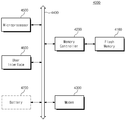
도 16은 본 발명에 따른 플래시 메모리 장치 및 그것을 포함하는 컴퓨팅 시스템의 개략적인 구성을 보여주는 도면이다.
110 : 셀 어레이 120 : 행 디코더
130 : 페이지 버퍼 회로 140 : 입출력 버퍼
150 : 제어 로직 160 : 전압 발생기
1000 : 사용자 장치
1100 : 호스트 1200 : 솔리드 스테이트 드라이브
1210 : SSD 컨트롤러 1220 : 버퍼 메모리
1230 : 불휘발성 메모리 장치
2000 : 메모리 시스템
2100 : 불휘발성 메모리 2200 : 메모리 컨트롤러
2210 : CPU 2220 : 호스트 인터페이스
2230 : SRAM 2240 : ECC
2250 : 메모리 인터페이스
3000 : 메모리 카드
3100 : 플래시 메모리 3200 : 플래시 컨트롤러
4000 : 컴퓨팅 시스템
4100 : 플래시 메모리 장치 4200 : 메모리 컨트롤러
4300 : 모뎀 4400 : 시스템 버스
4500 : 마이크로프로세서 4600 : 사용자 인터페이스
4700 : 배터리
Claims (10)
- 선택 워드 라인 및 제 1 비트 라인 그룹에 연결되고, 상기 제 1 비트 라인 그룹 내의 비트 라인들은 인접하는 제 1 메모리 셀 그룹;
상기 선택 워드 라인 및 제 2 비트 라인 그룹에 연결되고, 상기 제 2 비트 라인 그룹 내의 비트 라인들은 인접하는 제 2 메모리 셀 그룹;
상기 제 1 및 제 2 비트 라인 그룹을 통하여 상기 선택 워드 라인에 연결된 메모리 셀들을 센싱하는 페이지 버퍼 회로; 그리고
프로그램 동작 시에, 상기 제 1 메모리 셀 그룹에 대한 프로그램 동작을 수행한 후 상기 제 1 및 제 2 비트 라인 그룹에 연결된 비트 라인들을 동시에 프리차지하여 상기 제 1 메모리 셀 그룹에 대한 검증 동작을 수행하고, 상기 제 2 메모리 셀 그룹에 대한 프로그램 동작을 수행한 후 상기 제 1 및 제 2 비트 라인 그룹에 연결된 비트 라인들을 동시에 프리차지하여 상기 제 2 메모리 셀 그룹에 대한 검증 동작을 수행하는 제어 로직을 포함하되,
상기 제어 로직은 읽기 동작 시에 상기 제 1 및 제 2 비트 라인 그룹에 연결된 비트 라인들을 동시에 프리차지하여 읽기 동작을 수행하며, 미리 설정된 프로그램 반복 횟수에 따라 상기 제 1 메모리 셀 그룹을 먼저 프로그램한 후 상기 제 2 메모리 셀 그룹을 프로그램하도록 상기 페이지 버퍼 회로를 제어하는 불휘발성 메모리 장치. - 제 1 항에 있어서,
상기 제 1 비트 라인 그룹과 상기 제 2 비트 라인 그룹은 서로 동일한 수의 비트 라인들을 포함하는 불휘발성 메모리 장치. - 삭제
- 제 1 항에 있어서,
상기 제어 로직은 상기 읽기 동작 시에 상기 제 1 및 제 2 메모리 셀 그룹을 센싱하여 전체 페이지 읽기 모드 또는 부분 페이지 읽기 모드에 따라 출력하도록 상기 페이지 버퍼 회로를 제어하는 불휘발성 메모리 장치. - 제 4 항에 있어서,
상기 부분 페이지 읽기 모드 시에, 상기 페이지 버퍼 회로는 상기 제 1 및 제 2 비트 라인 그룹에 연결된 비트 라인들을 동시에 프리차지하여 센싱하는 불휘발성 메모리 장치. - 제 5 항에 있어서,
상기 부분 페이지 읽기 모드 시에, 상기 페이지 버퍼 회로는 읽기 요청에 따라 상기 제 1 메모리 셀 그룹 또는 제 2 메모리 셀 그룹 중 선택된 그룹으로부터 센싱된 데이터만 출력하는 불휘발성 메모리 장치. - 제 1 항에 있어서,
상기 제어 로직은 상기 제 1 비트 라인 그룹의 비트 라인들에 제 1 물리 어드레스들을 지정하고, 상기 제 2 비트 라인 그룹의 비트 라인들에 제 2 물리 어드레스들을 지정하는 불휘발성 메모리 장치. - 제 7 항에 있어서,
상기 제어 로직은 상기 제 1 물리 어드레스들을 쓰기 요청된 데이터의 제 1 논리 어드레스들에 순차적으로 어드레싱하는 불휘발성 메모리 장치. - 제 8 항에 있어서,
상기 제어 로직은 상기 제 2 물리 어드레스들을 쓰기 요청된 데이터의 제 2 논리 어드레스들에 순차적으로 어드레싱하고, 상기 제 2 논리 어드레스들은 상기 제 1 논리 어드레스들보다 나중에 어드레싱되는 불휘발성 메모리 장치. - 불휘발성 메모리 장치의 동작 방법에 있어서:
상기 불휘발성 메모리 장치는, 선택 워드 라인 및 제 1 비트 라인 그룹에 연결되고, 상기 제 1 비트 라인 그룹 내의 비트 라인들은 인접하는 제 1 메모리 셀 그룹; 상기 선택 워드 라인 및 제 2 비트 라인 그룹에 연결되고, 상기 제 2 비트 라인 그룹 불휘발성 메모리 장치의 동작 방법에 있어서:
상기 불휘발성 메모리 장치는, 선택 워드 라인 및 제 1 비트 라인 그룹에 연결되고, 상기 제 1 비트 라인 그룹 내의 비트 라인들은 인접하는 제 1 메모리 셀 그룹; 상기 선택 워드 라인 및 제 2 비트 라인 그룹에 연결되고, 상기 제 2 비트 라인 그룹 내의 비트 라인들은 인접하는 제 2 메모리 셀 그룹; 상기 제 1 및 제 2 비트 라인 그룹을 통하여 상기 선택 워드 라인에 연결된 메모리 셀들을 센싱하는 페이지 버퍼 회로; 그리고 상기 페이지 버퍼 회로를 제어하기 위한 제어 로직을 포함하되,
상기 불휘발성 메모리 장치의 동작 방법은,
상기 제 1 메모리 셀 그룹에 대한 프로그램 동작을 수행한 후 상기 제 1 및 제 2 비트 라인 그룹에 연결된 비트 라인들을 동시에 프리차지하여 상기 제 1 메모리 셀 그룹에 대한 검증 동작을 수행하고,
상기 제 1 메모리 셀 그룹에 대한 프로그램 검증 동작이 수행된 다음에, 상기 제 2 메모리 셀 그룹에 대한 프로그램 동작을 수행한 후 상기 제 1 및 제 2 비트 라인 그룹에 연결된 비트 라인들을 동시에 프리차지하여 상기 제 2 메모리 셀 그룹에 대한 검증 동작을 수행하고,
상기 제어 로직은, 미리 설정된 프로그램 반복 횟수에 따라 상기 제 1 메모리 셀 그룹을 먼저 프로그램한 후 상기 제 2 메모리 셀 그룹을 프로그램하도록 상기 페이지 버퍼 회로를 제어하고,
읽기 동작 시에 상기 제 1 및 제 2 비트 라인 그룹에 연결된 비트 라인들을 동시에 프리차지하여 읽기 동작을 수행하는 불휘발성 메모리 장치의 동작 방법.
Priority Applications (2)
| Application Number | Priority Date | Filing Date | Title |
|---|---|---|---|
| KR1020130153988A KR102128825B1 (ko) | 2013-12-11 | 2013-12-11 | 불휘발성 메모리 장치 및 그것의 동작 방법 |
| US14/506,841 US9524781B2 (en) | 2013-12-11 | 2014-10-06 | Nonvolatile memory device and operating method thereof |
Applications Claiming Priority (1)
| Application Number | Priority Date | Filing Date | Title |
|---|---|---|---|
| KR1020130153988A KR102128825B1 (ko) | 2013-12-11 | 2013-12-11 | 불휘발성 메모리 장치 및 그것의 동작 방법 |
Publications (2)
| Publication Number | Publication Date |
|---|---|
| KR20150068137A KR20150068137A (ko) | 2015-06-19 |
| KR102128825B1 true KR102128825B1 (ko) | 2020-07-01 |
Family
ID=53271198
Family Applications (1)
| Application Number | Title | Priority Date | Filing Date |
|---|---|---|---|
| KR1020130153988A Active KR102128825B1 (ko) | 2013-12-11 | 2013-12-11 | 불휘발성 메모리 장치 및 그것의 동작 방법 |
Country Status (2)
| Country | Link |
|---|---|
| US (1) | US9524781B2 (ko) |
| KR (1) | KR102128825B1 (ko) |
Families Citing this family (10)
| Publication number | Priority date | Publication date | Assignee | Title |
|---|---|---|---|---|
| KR102530071B1 (ko) * | 2016-03-02 | 2023-05-08 | 삼성전자주식회사 | 페이지 버퍼를 포함하는 불휘발성 메모리 장치 및 그 동작방법 |
| US10325657B2 (en) * | 2017-01-25 | 2019-06-18 | Samsung Electronics Co., Ltd. | Non-volatile memory devices and methods of programming the same |
| CN107437433A (zh) * | 2017-06-12 | 2017-12-05 | 中国科学院微电子研究所 | Nand闪存存储器的读操作方法、电子设备和计算机可读存储介质 |
| TWI640011B (zh) * | 2017-10-18 | 2018-11-01 | 力晶科技股份有限公司 | 非揮發性記憶體裝置及對其驗證的錯誤補償方法 |
| KR20190128283A (ko) * | 2018-05-08 | 2019-11-18 | 에스케이하이닉스 주식회사 | 컨트롤러, 메모리 시스템 및 그 동작방법 |
| KR102091524B1 (ko) * | 2018-07-23 | 2020-03-23 | 삼성전자주식회사 | 어드레스를 스크램블하는 메모리 장치 |
| US10636498B1 (en) * | 2019-02-22 | 2020-04-28 | Sandisk Technologies Llc | Managing bit-line settling time in non-volatile memory |
| KR102671597B1 (ko) * | 2019-07-31 | 2024-06-03 | 삼성전자주식회사 | 비휘발성 메모리 장치 및 비휘발성 메모리 장치의 초기화 제어 방법 |
| US11056200B2 (en) * | 2019-07-31 | 2021-07-06 | Samsung Electronics Co., Ltd. | Nonvolatile memory device and method of controlling initialization of the same |
| KR20210105734A (ko) * | 2020-02-19 | 2021-08-27 | 에스케이하이닉스 주식회사 | 메모리 장치 및 이의 동작 방법 |
Family Cites Families (19)
| Publication number | Priority date | Publication date | Assignee | Title |
|---|---|---|---|---|
| US7196931B2 (en) | 2002-09-24 | 2007-03-27 | Sandisk Corporation | Non-volatile memory and method with reduced source line bias errors |
| US7450430B2 (en) | 2006-12-29 | 2008-11-11 | Sandisk Corporation | Programming non-volatile memory with reduced program disturb by using different pre-charge enable voltages |
| US8169808B2 (en) | 2008-01-25 | 2012-05-01 | Micron Technology, Inc. | NAND flash content addressable memory |
| KR101462488B1 (ko) | 2008-03-31 | 2014-11-18 | 삼성전자주식회사 | 더미셀을 이용한 플래시 메모리 장치 및 그것의 동작 방법 |
| KR100954946B1 (ko) | 2008-05-20 | 2010-04-27 | 주식회사 하이닉스반도체 | 불휘발성 메모리 소자의 소거 방법 |
| KR20100058166A (ko) * | 2008-11-24 | 2010-06-03 | 삼성전자주식회사 | 불휘발성 메모리 장치 및 그것을 포함하는 메모리 시스템 |
| US8254174B2 (en) | 2009-02-04 | 2012-08-28 | Micron Technology, Inc. | Memory segment accessing in a memory device |
| KR101528886B1 (ko) * | 2009-04-09 | 2015-06-16 | 삼성전자주식회사 | 비휘발성 메모리 장치의 프로그램 방법 |
| KR20110001075A (ko) | 2009-06-29 | 2011-01-06 | 주식회사 하이닉스반도체 | 불휘발성 메모리 장치 및 그것의 동작 방법 |
| KR101012982B1 (ko) | 2009-06-30 | 2011-02-10 | 주식회사 하이닉스반도체 | 불휘발성 메모리 소자의 동작 방법 |
| US8169830B2 (en) | 2009-09-17 | 2012-05-01 | Micron Technology, Inc. | Sensing for all bit line architecture in a memory device |
| KR101771619B1 (ko) * | 2011-02-09 | 2017-08-28 | 삼성전자주식회사 | 불휘발성 메모리 장치 및 그것의 구동 방법 |
| KR101844963B1 (ko) * | 2011-03-07 | 2018-04-04 | 삼성전자주식회사 | 불 휘발성 메모리 장치 및 그것의 동작 방법 |
| KR101792870B1 (ko) * | 2011-06-21 | 2017-11-02 | 삼성전자주식회사 | 불휘발성 메모리 장치 및 그것의 읽기 방법 |
| KR20130079853A (ko) | 2012-01-03 | 2013-07-11 | 삼성전자주식회사 | 불휘발성 메모리 장치 및 그것을 포함하는 메모리 시스템 |
| KR101984796B1 (ko) * | 2012-05-03 | 2019-06-03 | 에스케이하이닉스 주식회사 | 반도체 메모리 장치, 그것을 포함하는 메모리 시스템 및 그것의 동작 방법 |
| KR101925018B1 (ko) * | 2012-06-19 | 2018-12-05 | 삼성전자주식회사 | 불휘발성 메모리 장치 |
| KR20130142406A (ko) * | 2012-06-19 | 2013-12-30 | 주식회사 포스코엘이디 | 조명장치용 렌즈 시트 |
| KR102083450B1 (ko) * | 2012-12-05 | 2020-03-02 | 삼성전자주식회사 | 페이지 버퍼를 포함하는 불휘발성 메모리 장치 및 그것의 동작 방법 |
-
2013
- 2013-12-11 KR KR1020130153988A patent/KR102128825B1/ko active Active
-
2014
- 2014-10-06 US US14/506,841 patent/US9524781B2/en active Active
Also Published As
| Publication number | Publication date |
|---|---|
| US20150160859A1 (en) | 2015-06-11 |
| KR20150068137A (ko) | 2015-06-19 |
| US9524781B2 (en) | 2016-12-20 |
Similar Documents
| Publication | Publication Date | Title |
|---|---|---|
| KR102302187B1 (ko) | 비휘발성 메모리 장치의 동작 방법 및 비휘발성 메모리 장치 | |
| KR102128825B1 (ko) | 불휘발성 메모리 장치 및 그것의 동작 방법 | |
| KR101792870B1 (ko) | 불휘발성 메모리 장치 및 그것의 읽기 방법 | |
| KR102609130B1 (ko) | 읽기 전압 서치 유닛을 포함하는 데이터 저장 장치 | |
| KR102402668B1 (ko) | 비휘발성 메모리 장치, 그것의 동작 방법 및 그것을 포함하는 저장 장치 | |
| KR101891164B1 (ko) | 프로그램 스케줄러를 포함하는 플래시 메모리 장치 | |
| KR102053953B1 (ko) | 불휘발성 메모리 장치를 포함하는 메모리 시스템 및 그것의 프로그램 방법 | |
| KR102083271B1 (ko) | 플래시 메모리의 물리적 특성을 이용하여 난수를 생성하는 플래시 메모리 시스템 및 그것의 난수 생성 방법 | |
| KR102585221B1 (ko) | 메모리 장치, 메모리 시스템 및 메모리 장치의 동작 방법 | |
| KR101944793B1 (ko) | 플래시 메모리를 포함하는 플래시 메모리 시스템 및 그것의 비정상 워드 라인 검출 방법 | |
| KR102118979B1 (ko) | 불휘발성 메모리 장치 및 그것의 프로그램 방법 | |
| US9281068B2 (en) | Nonvolatile memory and related reprogramming method | |
| KR102284658B1 (ko) | 비휘발성 메모리 장치, 이를 포함하는 메모리 시스템 및 상기 비휘발성 메모리 장치의 동작 방법 | |
| KR102452994B1 (ko) | 반도체 메모리 장치 및 그 동작 방법 | |
| KR20100107294A (ko) | 불휘발성 메모리 장치를 포함하는 메모리 시스템 및 불휘발성 메모리 장치의 프로그램 방법 | |
| KR102245822B1 (ko) | 불휘발성 메모리 장치를 포함하는 저장 장치 및 그것의 프로그램 방법 | |
| KR102359979B1 (ko) | 솔리드 스테이트 드라이브 장치 및 이를 포함하는 저장 시스템 | |
| US9576668B2 (en) | Semiconductor device and operating method thereof | |
| KR20150106778A (ko) | 메모리 시스템 및 메모리 시스템의 제어 방법 | |
| KR20100055906A (ko) | 멀티-레벨 비휘발성 메모리 장치, 상기 장치를 포함하는 메모리 시스템 및 그 동작 방법 | |
| KR20120046846A (ko) | 플래그 셀들을 갖는 플래시 메모리 장치 및 그것의 프로그램 동작 방법 | |
| CN111128280B (zh) | 存储装置及其操作方法 | |
| KR102182804B1 (ko) | 메모리 장치의 독출 방법 | |
| KR101642930B1 (ko) | 더미 셀을 갖는 불휘발성 메모리 장치 및 그것의 프로그램 방법 | |
| KR20100045739A (ko) | 불휘발성 메모리 장치, 그것의 프로그램 방법, 그리고 그것을 포함하는 메모리 시스템 |
Legal Events
| Date | Code | Title | Description |
|---|---|---|---|
| PA0109 | Patent application |
Patent event code: PA01091R01D Comment text: Patent Application Patent event date: 20131211 |
|
| PG1501 | Laying open of application | ||
| A201 | Request for examination | ||
| PA0201 | Request for examination |
Patent event code: PA02012R01D Patent event date: 20181121 Comment text: Request for Examination of Application Patent event code: PA02011R01I Patent event date: 20131211 Comment text: Patent Application |
|
| E902 | Notification of reason for refusal | ||
| PE0902 | Notice of grounds for rejection |
Comment text: Notification of reason for refusal Patent event date: 20200121 Patent event code: PE09021S01D |
|
| E701 | Decision to grant or registration of patent right | ||
| PE0701 | Decision of registration |
Patent event code: PE07011S01D Comment text: Decision to Grant Registration Patent event date: 20200617 |
|
| GRNT | Written decision to grant | ||
| PR0701 | Registration of establishment |
Comment text: Registration of Establishment Patent event date: 20200625 Patent event code: PR07011E01D |
|
| PR1002 | Payment of registration fee |
Payment date: 20200626 End annual number: 3 Start annual number: 1 |
|
| PG1601 | Publication of registration | ||
| PR1001 | Payment of annual fee |
Payment date: 20230524 Start annual number: 4 End annual number: 4 |
|
| PR1001 | Payment of annual fee |
Payment date: 20240527 Start annual number: 5 End annual number: 5 |