KR101425064B1 - Oxide thin film transistor and method of fabricating the same - Google Patents
Oxide thin film transistor and method of fabricating the same Download PDFInfo
- Publication number
- KR101425064B1 KR101425064B1 KR1020110055786A KR20110055786A KR101425064B1 KR 101425064 B1 KR101425064 B1 KR 101425064B1 KR 1020110055786 A KR1020110055786 A KR 1020110055786A KR 20110055786 A KR20110055786 A KR 20110055786A KR 101425064 B1 KR101425064 B1 KR 101425064B1
- Authority
- KR
- South Korea
- Prior art keywords
- electrode
- drain electrode
- gate
- data line
- active layer
- Prior art date
- Legal status (The legal status is an assumption and is not a legal conclusion. Google has not performed a legal analysis and makes no representation as to the accuracy of the status listed.)
- Active
Links
Images


Classifications
-
- H—ELECTRICITY
- H10—SEMICONDUCTOR DEVICES; ELECTRIC SOLID-STATE DEVICES NOT OTHERWISE PROVIDED FOR
- H10D—INORGANIC ELECTRIC SEMICONDUCTOR DEVICES
- H10D86/00—Integrated devices formed in or on insulating or conducting substrates, e.g. formed in silicon-on-insulator [SOI] substrates or on stainless steel or glass substrates
- H10D86/40—Integrated devices formed in or on insulating or conducting substrates, e.g. formed in silicon-on-insulator [SOI] substrates or on stainless steel or glass substrates characterised by multiple TFTs
- H10D86/60—Integrated devices formed in or on insulating or conducting substrates, e.g. formed in silicon-on-insulator [SOI] substrates or on stainless steel or glass substrates characterised by multiple TFTs wherein the TFTs are in active matrices
-
- H—ELECTRICITY
- H10—SEMICONDUCTOR DEVICES; ELECTRIC SOLID-STATE DEVICES NOT OTHERWISE PROVIDED FOR
- H10D—INORGANIC ELECTRIC SEMICONDUCTOR DEVICES
- H10D30/00—Field-effect transistors [FET]
- H10D30/60—Insulated-gate field-effect transistors [IGFET]
- H10D30/67—Thin-film transistors [TFT]
- H10D30/6729—Thin-film transistors [TFT] characterised by the electrodes
-
- H—ELECTRICITY
- H10—SEMICONDUCTOR DEVICES; ELECTRIC SOLID-STATE DEVICES NOT OTHERWISE PROVIDED FOR
- H10D—INORGANIC ELECTRIC SEMICONDUCTOR DEVICES
- H10D30/00—Field-effect transistors [FET]
- H10D30/60—Insulated-gate field-effect transistors [IGFET]
- H10D30/67—Thin-film transistors [TFT]
- H10D30/674—Thin-film transistors [TFT] characterised by the active materials
- H10D30/6755—Oxide semiconductors, e.g. zinc oxide, copper aluminium oxide or cadmium stannate
-
- H—ELECTRICITY
- H10—SEMICONDUCTOR DEVICES; ELECTRIC SOLID-STATE DEVICES NOT OTHERWISE PROVIDED FOR
- H10D—INORGANIC ELECTRIC SEMICONDUCTOR DEVICES
- H10D86/00—Integrated devices formed in or on insulating or conducting substrates, e.g. formed in silicon-on-insulator [SOI] substrates or on stainless steel or glass substrates
- H10D86/01—Manufacture or treatment
- H10D86/021—Manufacture or treatment of multiple TFTs
- H10D86/0231—Manufacture or treatment of multiple TFTs using masks, e.g. half-tone masks
-
- H—ELECTRICITY
- H10—SEMICONDUCTOR DEVICES; ELECTRIC SOLID-STATE DEVICES NOT OTHERWISE PROVIDED FOR
- H10D—INORGANIC ELECTRIC SEMICONDUCTOR DEVICES
- H10D86/00—Integrated devices formed in or on insulating or conducting substrates, e.g. formed in silicon-on-insulator [SOI] substrates or on stainless steel or glass substrates
- H10D86/40—Integrated devices formed in or on insulating or conducting substrates, e.g. formed in silicon-on-insulator [SOI] substrates or on stainless steel or glass substrates characterised by multiple TFTs
- H10D86/421—Integrated devices formed in or on insulating or conducting substrates, e.g. formed in silicon-on-insulator [SOI] substrates or on stainless steel or glass substrates characterised by multiple TFTs having a particular composition, shape or crystalline structure of the active layer
- H10D86/423—Integrated devices formed in or on insulating or conducting substrates, e.g. formed in silicon-on-insulator [SOI] substrates or on stainless steel or glass substrates characterised by multiple TFTs having a particular composition, shape or crystalline structure of the active layer comprising semiconductor materials not belonging to the Group IV, e.g. InGaZnO
-
- H—ELECTRICITY
- H10—SEMICONDUCTOR DEVICES; ELECTRIC SOLID-STATE DEVICES NOT OTHERWISE PROVIDED FOR
- H10D—INORGANIC ELECTRIC SEMICONDUCTOR DEVICES
- H10D86/00—Integrated devices formed in or on insulating or conducting substrates, e.g. formed in silicon-on-insulator [SOI] substrates or on stainless steel or glass substrates
- H10D86/40—Integrated devices formed in or on insulating or conducting substrates, e.g. formed in silicon-on-insulator [SOI] substrates or on stainless steel or glass substrates characterised by multiple TFTs
- H10D86/441—Interconnections, e.g. scanning lines
-
- H—ELECTRICITY
- H10—SEMICONDUCTOR DEVICES; ELECTRIC SOLID-STATE DEVICES NOT OTHERWISE PROVIDED FOR
- H10D—INORGANIC ELECTRIC SEMICONDUCTOR DEVICES
- H10D30/00—Field-effect transistors [FET]
- H10D30/01—Manufacture or treatment
- H10D30/021—Manufacture or treatment of FETs having insulated gates [IGFET]
- H10D30/031—Manufacture or treatment of FETs having insulated gates [IGFET] of thin-film transistors [TFT]
- H10D30/0312—Manufacture or treatment of FETs having insulated gates [IGFET] of thin-film transistors [TFT] characterised by the gate electrodes
- H10D30/0316—Manufacture or treatment of FETs having insulated gates [IGFET] of thin-film transistors [TFT] characterised by the gate electrodes of lateral bottom-gate TFTs comprising only a single gate
-
- H—ELECTRICITY
- H10—SEMICONDUCTOR DEVICES; ELECTRIC SOLID-STATE DEVICES NOT OTHERWISE PROVIDED FOR
- H10D—INORGANIC ELECTRIC SEMICONDUCTOR DEVICES
- H10D30/00—Field-effect transistors [FET]
- H10D30/01—Manufacture or treatment
- H10D30/021—Manufacture or treatment of FETs having insulated gates [IGFET]
- H10D30/031—Manufacture or treatment of FETs having insulated gates [IGFET] of thin-film transistors [TFT]
- H10D30/0321—Manufacture or treatment of FETs having insulated gates [IGFET] of thin-film transistors [TFT] comprising silicon, e.g. amorphous silicon or polysilicon
-
- H—ELECTRICITY
- H10—SEMICONDUCTOR DEVICES; ELECTRIC SOLID-STATE DEVICES NOT OTHERWISE PROVIDED FOR
- H10D—INORGANIC ELECTRIC SEMICONDUCTOR DEVICES
- H10D62/00—Semiconductor bodies, or regions thereof, of devices having potential barriers
- H10D62/80—Semiconductor bodies, or regions thereof, of devices having potential barriers characterised by the materials
-
- H10P95/00—
Landscapes
- Thin Film Transistor (AREA)
- Liquid Crystal (AREA)
- Electroluminescent Light Sources (AREA)
Abstract
본 발명의 산화물 박막 트랜지스터 및 그 제조방법은 이종(異種)의 금속물질로 제 1, 제 2 데이터 배선을 형성하는 한편, 상기 제 1 데이터 배선 위에 액티브층을 형성함으로써 단채널(short channel)을 구현하여 박막 트랜지스터의 성능을 향상시키기 위한 것으로, 기판 위에 제 1 도전막으로 이루어진 게이트전극 및 게이트라인을 형성하는 단계; 상기 게이트전극 및 게이트라인이 형성된 기판 위에 게이트절연막을 형성하는 단계; 하프-톤 노광을 이용하여 상기 게이트절연막이 형성된 게이트전극 상부에 제 2 도전막으로 이루어진 소오스전극과 연장부를 가진 제 1 드레인전극 및 제 1 데이터라인을 형성하는 한편, 상기 제 1 드레인전극의 연장부 및 상기 제 1 데이터라인 위에 제 3 도전막으로 이루어진 제 2 드레인전극 및 제 2 데이터라인을 각각 형성하는 단계; 상기 소오스전극 및 제 1 드레인전극 위에 산화물 반도체로 이루어진 액티브층을 형성하는 단계; 상기 액티브층이 형성된 기판 위에 보호막을 형성하는 단계; 및 상기 보호막 위에 상기 제 2 드레인전극과 전기적으로 접속하는 화소전극을 형성하는 단계를 포함하며, 상기 액티브층과 제 2 드레인전극은 상기 소오스전극 및 제 1 드레인전극이 형성된 기판 위의 동일층에 형성되는 것을 특징으로 한다.
이때, 상기 액티브층에 접촉하는 제 1 데이터 배선은 접촉특성이 우수한 금속물질로 형성하고, 나머지 제 2 데이터 배선은 전도도가 우수한 금속물질로 형성함으로써 대면적 산화막 박막 트랜지스터 공정에 활용 가능하게 된다. 또한, 상기 제 1, 제 2 데이터 배선은 하프-톤(halftone) 노광을 이용하여 함께 형성할 수 있으며, 이 경우 공정이 단순화되게 된다.The oxide thin film transistor and the method for fabricating the same of the present invention can form a short channel by forming first and second data lines with different kinds of metal materials and forming an active layer on the first data line. Forming a gate electrode and a gate line made of a first conductive film on a substrate; Forming a gate insulating film on the substrate on which the gate electrode and the gate line are formed; A first drain electrode and a first data line having a source electrode made of a second conductive film and an extended portion and a first data line are formed on the gate electrode on which the gate insulating film is formed by using half-tone exposure, And forming a second drain electrode and a second data line each made of a third conductive film on the first data line; Forming an active layer made of an oxide semiconductor on the source electrode and the first drain electrode; Forming a protective film on the substrate on which the active layer is formed; And forming a pixel electrode electrically connected to the second drain electrode on the protective layer, wherein the active layer and the second drain electrode are formed on the same layer on the substrate on which the source electrode and the first drain electrode are formed .
At this time, the first data wiring contacting the active layer is formed of a metal material having excellent contact characteristics, and the remaining second data wiring is formed of a metal material having excellent conductivity, so that the present invention can be utilized in a large area oxide film transistor process. In addition, the first and second data lines may be formed together using a halftone exposure, in which case the process is simplified.
Description
본 발명은 산화물 박막 트랜지스터 및 그 제조방법에 관한 것으로, 보다 상세하게는 산화물 반도체를 액티브층으로 사용한 산화물 박막 트랜지스터 및 그 제조방법에 관한 것이다.The present invention relates to an oxide thin film transistor and a manufacturing method thereof, and more particularly, to an oxide thin film transistor using an oxide semiconductor as an active layer and a manufacturing method thereof.
최근 정보 디스플레이에 관한 관심이 고조되고 휴대가 가능한 정보매체를 이용하려는 요구가 높아지면서 기존의 표시장치인 브라운관(Cathode Ray Tube; CRT)을 대체하는 경량 박막형 평판표시장치(Flat Panel Display; FPD)에 대한 연구 및 상업화가 중점적으로 이루어지고 있다. 특히, 이러한 평판표시장치 중 액정표시장치(Liquid Crystal Display; LCD)는 액정의 광학적 이방성을 이용하여 이미지를 표현하는 장치로서, 해상도와 컬러표시 및 화질 등에서 우수하여 노트북이나 데스크탑 모니터 등에 활발하게 적용되고 있다.Recently, interest in information display has increased, and a demand for using portable information media has increased, and a light-weight flat panel display (FPD) that replaces a cathode ray tube (CRT) And research and commercialization are being carried out. Particularly, among such flat panel display devices, a liquid crystal display (LCD) is an apparatus for displaying an image using the optical anisotropy of a liquid crystal, and is excellent in resolution, color display and picture quality and is actively applied to a notebook or a desktop monitor have.
상기 액정표시장치는 크게 컬러필터(color filter) 기판과 어레이(array) 기판 및 상기 컬러필터 기판과 어레이 기판 사이에 형성된 액정층(liquid crystal layer)으로 구성된다.The liquid crystal display comprises a color filter substrate, an array substrate, and a liquid crystal layer formed between the color filter substrate and the array substrate.
상기 액정표시장치에 주로 사용되는 구동 방식인 능동 매트릭스(Active Matrix; AM) 방식은 비정질 실리콘 박막 트랜지스터(Amorphous Silicon Thin Film Transistor; a-Si TFT)를 스위칭소자로 사용하여 화소부의 액정을 구동하는 방식이다.An active matrix (AM) method, which is a driving method mainly used in the liquid crystal display, is a method of driving a liquid crystal of a pixel portion by using an amorphous silicon thin film transistor (a-Si TFT) to be.
이하, 도 1을 참조하여 일반적인 액정표시장치에 대해서 상세히 설명한다.Hereinafter, a general liquid crystal display device will be described in detail with reference to FIG.
도 1은 일반적인 액정표시장치의 구조를 개략적으로 나타내는 분해사시도이다.1 is an exploded perspective view schematically showing a structure of a general liquid crystal display device.
도면에 도시된 바와 같이, 상기 액정표시장치는 크게 컬러필터 기판(5)과 어레이 기판(10) 및 상기 컬러필터 기판(5)과 어레이 기판(10) 사이에 형성된 액정층(liquid crystal layer)(30)으로 구성된다.As shown in the figure, the liquid crystal display comprises a
상기 컬러필터 기판(5)은 적(Red; R), 녹(Green; G) 및 청(Blue; B)의 색상을 구현하는 다수의 서브-컬러필터(7)로 구성된 컬러필터(C)와 상기 서브-컬러필터(7) 사이를 구분하고 액정층(30)을 투과하는 광을 차단하는 블랙매트릭스(black matrix)(6), 그리고 상기 액정층(30)에 전압을 인가하는 투명한 공통전극(8)으로 이루어져 있다.The
상기 어레이 기판(10)은 종횡으로 배열되어 복수개의 화소영역(P)을 정의하는 복수개의 게이트라인(16)과 데이터라인(17), 상기 게이트라인(16)과 데이터라인(17)의 교차영역에 형성된 스위칭소자인 박막 트랜지스터(T) 및 상기 화소영역(P) 위에 형성된 화소전극(18)으로 이루어져 있다.The
이와 같이 구성된 상기 컬러필터 기판(5)과 어레이 기판(10)은 화상표시 영역의 외곽에 형성된 실런트(sealant)(미도시)에 의해 대향하도록 합착되어 패널을 구성하며, 이때 상기 컬러필터 기판(5)과 어레이 기판(10)의 합착은 상기 컬러필터 기판(5) 또는 어레이 기판(10)에 형성된 합착키(미도시)를 통해 이루어진다.The
한편, 전술한 액정표시장치는 가볍고 전력소모가 작아 지금가지 가장 주목받는 디스플레이 소자지만, 상기 액정표시장치는 발광소자가 아니라 수광소자이며 밝기, 명암비(contrast ratio) 및 시야각 등에 기술적 한계가 있기 때문에 이러한 단점을 극복할 수 있는 새로운 디스플레이 소자에 대한 개발이 활발하게 전개되고 있다.However, the liquid crystal display device is not a light emitting device but a light receiving device and has technical limitations on brightness, contrast ratio, viewing angle, etc. Therefore, Development of a new display device capable of overcoming the disadvantages has been actively developed.
새로운 평판표시장치 중 하나인 유기전계발광소자(Organic Light Emitting Diode; OLED)는 자체발광형이기 때문에 액정표시장치에 비해 시야각과 명암비 등이 우수하며 백라이트(backlight)가 필요하지 않기 때문에 경량 박형이 가능하고, 소비전력 측면에서도 유리하다. 그리고, 직류 저전압 구동이 가능하고 응답속도가 빠르다는 장점이 있으며, 특히 제조비용 측면에서도 유리한 장점을 가지고 있다.OLED (Organic Light Emitting Diode), which is one of the new flat panel display devices, has excellent viewing angle and contrast ratio compared to liquid crystal displays because it is a self-luminous type. Lightweight thin type can be used because it does not need backlight And is also advantageous in terms of power consumption. In addition, it has the advantage of being able to drive a DC low voltage and has a high response speed, and is particularly advantageous in terms of manufacturing cost.
최근 유기전계발광 디스플레이의 대면적화에 관한 연구가 활발하게 진행되고 있으며, 이를 달성하기 위하여 유기전계발광소자의 구동 트랜지스터로서 정전류 특성을 확보하여 안정된 작동 및 내구성이 확보된 박막 트랜지스터 개발이 요구되고 있다.In recent years, studies have been actively made on the large-sized organic electroluminescent display. In order to achieve this, it is required to develop a thin film transistor having stable operation and durability by securing a constant current characteristic as a driving transistor of an organic electroluminescent device.
전술한 액정표시장치에 사용되는 비정질 실리콘 박막 트랜지스터는 저온 공정에서 제작할 수 있지만 이동도(mobility)가 매우 작고 정전류 테스트(constant current bias) 조건을 만족하지 않는다. 반면에 다결정 실리콘 박막 트랜지스터는 높은 이동도와 만족스러운 정전류 테스트 조건을 가지는 반면에 균일한 특성 확보가 어려워 대면적화가 어렵고 고온 공정이 필요하다.The amorphous silicon thin film transistor used in the above-described liquid crystal display device can be manufactured in a low temperature process, but has a very small mobility and does not satisfy a constant current bias condition. On the other hand, the polycrystalline silicon thin film transistor has a high mobility and a satisfactory constant current test condition, but it is difficult to obtain a uniform characteristic, so it is difficult to make a large area and a high temperature process is required.
이에 산화물 반도체로 액티브층을 형성한 산화물 박막 트랜지스터가 개발되고 있는데, 이때 상기 산화물 반도체를 기존의 하부 게이트(bottom gate) 구조의 박막 트랜지스터에 적용하는 경우 소오스/드레인전극의 식각공정, 특히 플라즈마를 이용한 건식각(dry etching) 중에 산화물 반도체가 손상을 받아 변성을 일으키는 문제점이 있다.An oxide thin film transistor in which an active layer is formed of an oxide semiconductor has been developed. In this case, when the oxide semiconductor is applied to a conventional thin film transistor having a bottom gate structure, the etching process of the source / drain electrode, There is a problem that the oxide semiconductor is damaged during dry etching to cause denaturation.
이를 방지하기 위해 에치 스타퍼(etch stopper)를 액티브층 상부에 추가로 형성하기도 하는데, 이 경우 10㎛이하의 단채널(short channel) 구현이 어렵고 포토리소그래피(photolithography)공정(이하, 포토공정이라 함)이 추가되는 단점이 있다.In order to prevent this, an etch stopper may be additionally formed on the active layer. In this case, it is difficult to realize a short channel of 10 μm or less and a photolithography process (hereinafter referred to as a photo process) ) Is added.
도 2는 일반적인 산화물 박막 트랜지스터를 개략적으로 나타내는 단면도이다.2 is a cross-sectional view schematically showing a general oxide thin film transistor.
도면에 도시된 바와 같이, 일반적인 산화물 박막 트랜지스터는 소정의 기판(10) 위에 형성된 게이트전극(21), 상기 게이트전극(21) 위에 형성된 게이트절연막(15a), 상기 게이트절연막(15a) 위에 산화물 반도체로 형성된 액티브층(24)과 소정의 절연물질로 형성된 에치 스타퍼(25), 상기 액티브층(24)의 소정영역과 전기적으로 접속하는 소오스/드레인전극(22, 23), 상기 소오스/드레인전극(22, 23) 위에 형성된 보호막(15b) 및 상기 드레인전극(23)과 전기적으로 접속하는 화소전극(18)으로 이루어져 있다.As shown in the figure, a general oxide thin film transistor includes a
도 3a 내지 도 3f는 상기 도 2에 도시된 일반적인 산화물 박막 트랜지스터의 제조공정을 순차적으로 나타내는 단면도이다.FIGS. 3A to 3F are cross-sectional views sequentially illustrating the manufacturing process of the general oxide thin film transistor shown in FIG.
도 3a에 도시된 바와 같이, 소정의 기판(10) 전면(全面)에 제 1 도전막을 증착한 후, 포토공정을 통해 선택적으로 패터닝함으로써 상기 기판(10) 위에 상기 제 1 도전막으로 이루어진 게이트전극(21)을 형성한다.3A, a first conductive film is deposited on the entire surface of a
다음으로, 도 3b에 도시된 바와 같이, 상기 기판(10) 전면에 차례대로 게이트절연막(15a)과 소정의 산화물 반도체로 이루어진 산화물 반도체층을 증착한 후, 포토공정을 이용하여 선택적으로 패터닝함으로써 상기 게이트전극(21) 상부에 상기 산화물 반도체로 이루어진 액티브층(24)을 형성한다.Next, as shown in FIG. 3B, an oxide semiconductor layer made of a predetermined oxide semiconductor and a
그리고, 도 3c에 도시된 바와 같이, 상기 기판(10) 전면에 소정의 절연물질로 이루어진 절연층을 증착한 후, 포토공정을 이용하여 선택적으로 패터닝함으로써 상기 액티브층(24) 상부에 상기 절연물질로 이루어진 에치 스타퍼(25)를 형성한다.3C, an insulating layer made of a predetermined insulating material is deposited on the entire surface of the
다음으로, 도 3d에 도시된 바와 같이, 상기 에치 스타퍼(25)가 형성된 기판(10) 전면에 제 2 도전막을 형성한 후, 포토공정을 통해 선택적으로 패터닝함으로써 상기 액티브층(24)과 에치 스타퍼(25) 상부에 상기 제 2 도전막으로 이루어지며 상기 액티브층(24)의 소오스/드레인영역과 전기적으로 접속하는 소오스/드레인전극(22, 23)을 형성하게 된다.3D, a second conductive layer is formed on the entire surface of the
다음으로, 도 3e에 도시된 바와 같이, 상기 소오스/드레인전극(22, 23)이 형성된 기판(10) 전면에 소정의 보호막(15b)을 형성한 후, 포토공정을 통해 선택적으로 패터닝함으로써 상기 드레인전극(23)의 일부를 노출시키는 콘택홀(40)을 형성하게 된다.Next, as shown in FIG. 3E, a predetermined
그리고, 도 3f에 도시된 바와 같이, 상기 기판(10) 전면에 제 3 도전막을 형성한 후, 포토공정을 통해 선택적으로 패터닝함으로써 상기 콘택홀을 통해 상기 드레인전극(23)과 전기적으로 접속하는 화소전극(18)을 형성하게 된다.3F, a third conductive film is formed on the entire surface of the
이와 같이 상기 구조의 산화물 박막 트랜지스터를 제조하기 위해서는 에치 스타퍼를 형성하기 위한 추가적인 포토공정이 필요하며, 또한 상기 에치 스타퍼의 사용으로 10㎛이하의 단채널 구현이 어려운 단점이 있다. 즉, 빠른 이동도 장점을 유기전계발광소자에 적용하기 위해서는 단채널 구현이 필요하나, 에치 스타퍼의 선 폭으로 채널 길이가 결정되며, 게이트전극과 에치 스타퍼 및 소오스/드레인전극 간의 설계마진에 정밀도가 요구되므로 10㎛이하의 단채널 구현이 어렵게 된다.In order to manufacture an oxide thin film transistor having such a structure, an additional photolithography process is required to form an etch stopper. Further, it is difficult to realize a single channel of 10 μm or less by using the etch stopper. That is, in order to apply the advantage of fast movement to the organic electroluminescent device, it is necessary to realize a short channel, but the channel length is determined by the line width of the etch stopper, and the design margin between the gate electrode and the etch stopper and the source / Precision is required, it is difficult to realize a short channel of 10 μm or less.
본 발명은 상기한 문제를 해결하기 위한 것으로, 산화물 반도체를 액티브층으로 사용하여 대면적 디스플레이에 적용하도록 한 산화물 박막 트랜지스터 및 그 제조방법을 제공하는데 목적이 있다.An object of the present invention is to provide an oxide thin film transistor and a method of manufacturing the same, in which an oxide semiconductor is used as an active layer and applied to a large area display.
본 발명의 다른 목적은 대면적 산화물 박막 트랜지스터의 성능을 향상시키는 동시에 공정을 단순화 한 산화물 박막 트랜지스터 및 그 제조방법을 제공하는데 있다.It is another object of the present invention to provide an oxide thin film transistor which simplifies the process while improving the performance of a large area oxide thin film transistor and a method of manufacturing the same.
본 발명의 다른 목적 및 특징들은 후술되는 발명의 구성 및 특허청구범위에서 설명될 것이다.Other objects and features of the present invention will be described in the following description of the invention and claims.
상기한 목적을 달성하기 위하여, 본 발명의 산화물 박막 트랜지스터의 제조방법은 기판 위에 제 1 도전막으로 이루어진 게이트전극 및 게이트라인을 형성하는 단계; 상기 게이트전극 및 게이트라인이 형성된 기판 위에 게이트절연막을 형성하는 단계; 하프-톤 노광을 이용하여 상기 게이트절연막이 형성된 게이트전극 상부에 제 2 도전막으로 이루어진 소오스전극과 연장부를 가진 제 1 드레인전극 및 제 1 데이터라인을 형성하는 한편, 상기 제 1 드레인전극의 연장부 및 상기 제 1 데이터라인 위에 제 3 도전막으로 이루어진 제 2 드레인전극 및 제 2 데이터라인을 각각 형성하는 단계; 상기 소오스전극 및 제 1 드레인전극 위에 산화물 반도체로 이루어진 액티브층을 형성하는 단계; 상기 액티브층이 형성된 기판 위에 보호막을 형성하는 단계; 및 상기 보호막 위에 상기 제 2 드레인전극과 전기적으로 접속하는 화소전극을 형성하는 단계를 포함하며, 상기 액티브층과 제 2 드레인전극은 상기 소오스전극 및 제 1 드레인전극이 형성된 기판 위의 동일층에 형성되는 것을 특징으로 한다.According to an aspect of the present invention, there is provided a method of fabricating an oxide thin film transistor, including: forming a gate electrode and a gate line made of a first conductive film on a substrate; Forming a gate insulating film on the substrate on which the gate electrode and the gate line are formed; A first drain electrode and a first data line having a source electrode made of a second conductive film and an extended portion and a first data line are formed on the gate electrode on which the gate insulating film is formed by using half-tone exposure, And forming a second drain electrode and a second data line each made of a third conductive film on the first data line; Forming an active layer made of an oxide semiconductor on the source electrode and the first drain electrode; Forming a protective film on the substrate on which the active layer is formed; And forming a pixel electrode electrically connected to the second drain electrode on the protective layer, wherein the active layer and the second drain electrode are formed on the same layer on the substrate on which the source electrode and the first drain electrode are formed .
이때, 상기 액티브층은 비정질 아연 산화물계 반도체로 형성하는 것을 특징으로 한다.In this case, the active layer is formed of an amorphous zinc oxide-based semiconductor.
상기 제 2 도전막은 상기 액티브층 및 게이트절연막과의 접촉특성이 우수하고 상기 액티브층과 오믹-콘택이 우수한 몰리브덴 티타늄(MoTi), 인듐-틴-옥사이드(Indium Tin Oxide; ITO), 티타늄(Ti) 또는 몰리브덴(Mo) 등의 금속물질로 형성하는 것을 특징으로 한다.The second conductive layer may be formed of at least one selected from the group consisting of molybdenum titanium (MoTi), indium tin oxide (ITO), and titanium (Ti), which have excellent contact properties with the active layer and the gate insulating layer, Or a metal material such as molybdenum (Mo).
상기 제 3 도전막은 상기 제 2 도전막과 이종의 금속물질로 전도도가 우수한 알루미늄, 구리, 은, 금 등의 금속물질로 형성하는 것을 특징으로 한다.The third conductive layer may be formed of a different metal material from the second conductive layer, and may be formed of a metal material such as aluminum, copper, silver, gold, or the like having excellent conductivity.
상기 액티브층은 상기 제 2 데이터라인과 제 2 드레인전극 사이에 위치하는 아일랜드 형태로 형성하는 것을 특징으로 한다. And the active layer is formed in an island shape located between the second data line and the second drain electrode.
본 발명의 산화물 박막 트랜지스터의 다른 제조방법은 기판 위에 게이트전극 및 게이트라인을 형성하는 단계; 상기 게이트전극 및 게이트라인이 형성된 기판 위에 게이트절연막을 형성하는 단계; 상기 게이트절연막이 형성된 게이트전극 상부에 제 1 소오스전극과 제 1 드레인전극 및 제 1 데이터라인을 형성하는 단계; 상기 제 1 소오스전극 및 제 1 드레인전극 위에 산화물 반도체로 이루어진 액티브층을 형성하는 단계; 상기 액티브층 위에 에치 스타퍼를 형성하는 단계; 및 상기 에치 스타퍼가 형성된 액티브층 상부에 제 2 소오스전극과 제 2 드레인전극을 형성하며, 상기 제 1 데이터라인 위에 제 2 데이터라인을 형성하는 단계를 포함한다.Another method of manufacturing an oxide thin film transistor of the present invention includes forming a gate electrode and a gate line on a substrate; Forming a gate insulating film on the substrate on which the gate electrode and the gate line are formed; Forming a first source electrode, a first drain electrode and a first data line above a gate electrode on which the gate insulating film is formed; Forming an active layer made of an oxide semiconductor on the first source electrode and the first drain electrode; Forming an etch stopper over the active layer; And forming a second source electrode and a second drain electrode on the active layer on which the etch stopper is formed, and forming a second data line on the first data line.
이때, 상기 제 1 드레인전극과 제 2 드레인전극은 화소영역으로 연장된 연장부를 가지며, 상기 제 1 드레인전극의 연장부 위에 상기 제 2 드레인전극의 연장부가 형성되는 것을 특징으로 한다.Here, the first drain electrode and the second drain electrode may have extended portions extending to the pixel region, and an extension of the second drain electrode may be formed on the extension of the first drain electrode.
본 발명의 산화물 박막 트랜지스터는 기판 위에 제 1 도전막으로 형성된 게이트전극 및 게이트라인; 상기 게이트전극 및 게이트라인이 형성된 기판 위에 형성된 게이트절연막; 상기 게이트절연막이 형성된 게이트전극 상부에 제 2 도전막으로 형성된 소오스전극과 연장부를 가진 제 1 드레인전극 및 제 1 데이터라인; 상기 제 1 드레인전극의 연장부 및 상기 제 1 데이터라인 위에 제 3 도전막으로 각각 형성된 제 2 드레인전극 및 제 2 데이터라인; 상기 소오스전극 및 제 1 드레인전극 위에 산화물 반도체로 형성된 액티브층; 상기 액티브층이 형성된 기판 위에 형성된 보호막; 및 상기 보호막 위에 형성되어 상기 제 2 드레인전극과 전기적으로 접속하는 화소전극을 포함하며, 상기 액티브층과 제 2 드레인전극은 상기 소오스전극 및 제 1 드레인전극이 형성된 기판 위의 동일층에 위치하는 것을 특징으로 한다.The oxide thin film transistor of the present invention comprises: a gate electrode and a gate line formed on a substrate with a first conductive film; A gate insulating film formed on the substrate on which the gate electrode and the gate line are formed; A first drain electrode and a first data line having a source electrode and an extended portion formed of a second conductive film over the gate electrode on which the gate insulating film is formed; A second drain electrode and a second data line respectively formed as an extension of the first drain electrode and a third conductive film on the first data line; An active layer formed of an oxide semiconductor on the source electrode and the first drain electrode; A protective film formed on the substrate on which the active layer is formed; And a pixel electrode formed on the protective film and electrically connected to the second drain electrode, wherein the active layer and the second drain electrode are located on the same layer on the substrate on which the source electrode and the first drain electrode are formed .
이때, 상기 액티브층은 비정질 아연 산화물계 반도체로 이루어진 것을 특징으로 한다.In this case, the active layer is formed of an amorphous zinc oxide-based semiconductor.
상기 제 2 도전막은 상기 액티브층 및 게이트절연막과의 접촉특성이 우수하고 상기 액티브층과 오믹-콘택이 우수한 몰리브덴 티타늄(MoTi), 인듐-틴-옥사이드(Indium Tin Oxide; ITO), 티타늄(Ti) 또는 몰리브덴(Mo) 등의 금속물질로 이루어진 것을 특징으로 한다.The second conductive layer may be formed of at least one selected from the group consisting of molybdenum titanium (MoTi), indium tin oxide (ITO), and titanium (Ti), which have excellent contact properties with the active layer and the gate insulating layer, Or molybdenum (Mo).
상기 제 3 도전막은 상기 제 2 도전막과 이종의 금속물질로 전도도가 우수한 알루미늄, 구리, 은, 금 등의 금속물질로 이루어진 것을 특징으로 한다.The third conductive layer is made of a different metal material from the second conductive layer, and is made of a metal material such as aluminum, copper, silver, or gold, which has excellent conductivity.
상기 액티브층은 상기 제 2 데이터라인과 제 2 드레인전극 사이에 위치하는 아일랜드 형태로 이루어진 것을 특징으로 한다.And the active layer is formed in an island shape located between the second data line and the second drain electrode.
본 발명의 다른 산화물 박막 트랜지스터는 기판 위에 형성된 게이트전극 및 게이트라인; 상기 게이트전극 및 게이트라인이 형성된 기판 위에 형성된 게이트절연막; 상기 게이트절연막이 형성된 게이트전극 상부에 형성된 제 1 소오스전극과 제 1 드레인전극 및 제 1 데이터라인; 상기 제 1 소오스전극 및 제 1 드레인전극 위에 산화물 반도체로 형성된 액티브층; 상기 액티브층 위에 형성된 에치 스타퍼; 상기 에치 스타퍼가 형성된 액티브층 상부에 형성된 제 2 소오스전극과 제 2 드레인전극; 상기 제 1 데이터라인 위에 형성된 제 2 데이터라인을 포함한다.Another oxide thin film transistor of the present invention includes a gate electrode and a gate line formed on a substrate; A gate insulating film formed on the substrate on which the gate electrode and the gate line are formed; A first source electrode, a first drain electrode, and a first data line formed on the gate electrode on which the gate insulating layer is formed; An active layer formed of an oxide semiconductor on the first source electrode and the first drain electrode; An etch stopper formed over the active layer; A second source electrode and a second drain electrode formed on the active layer on which the etch stopper is formed; And a second data line formed on the first data line.
이때, 상기 제 1 드레인전극과 제 2 드레인전극은 화소영역으로 연장된 연장부를 가지며, 상기 제 1 드레인전극의 연장부 위에 상기 제 2 드레인전극의 연장부가 위치하는 것을 특징으로 한다.Here, the first drain electrode and the second drain electrode may have extended portions extending to the pixel region, and the extended portion of the second drain electrode may be located on the extended portion of the first drain electrode.
상기 액티브층의 제 1 소오스/드레인영역은 상기 제 1 소오스/드레인전극과 전기적으로 접속하는 한편, 상기 액티브층의 제 2 소오스/드레인영역은 상기 제 2 소오스/드레인전극과 전기적으로 접속하는 것을 특징으로 한다.The first source / drain region of the active layer is electrically connected to the first source / drain electrode, and the second source / drain region of the active layer is electrically connected to the second source / drain electrode. .
상술한 바와 같이, 본 발명에 따른 산화물 박막 트랜지스터 및 그 제조방법은 비정질 산화물 반도체를 액티브층으로 사용함에 따라 균일도가 우수하여 대면적 디스플레이에 적용 가능한 효과를 제공한다.As described above, the oxide thin film transistor and the method of manufacturing the same according to the present invention have an excellent uniformity due to the use of an amorphous oxide semiconductor as an active layer, thereby providing an effect applicable to a large area display.
본 발명에 따른 산화물 박막 트랜지스터 및 그 제조방법은 4㎛ ~ 10㎛의 단채널을 구현함에 따라 온 전류(on current)의 향상, 기생 커패시턴스(parasitic capacitance)의 감소 등 대면적 산화물 박막 트랜지스터의 성능을 향상시키는 효과를 제공한다.The oxide thin film transistor and the method of manufacturing the same according to the present invention can improve the on-current and the parasitic capacitance by realizing a short channel of 4 탆 to 10 탆. Thereby providing an effect of improving the performance.
본 발명에 따른 산화물 박막 트랜지스터 및 그 제조방법은 에치 스타퍼를 제거할 수 있어 포토공정의 삭제로 공정이 단순화되는 효과를 제공한다.The oxide thin film transistor and the manufacturing method thereof according to the present invention can remove the etch stopper, thereby simplifying the process by eliminating the photo process.
본 발명에 따른 산화물 박막 트랜지스터 및 그 제조방법은 액티브층 상, 하부에 소오스/드레인전극을 형성하여 액티브층과의 접촉 면적을 증가시킬 수 있으며, 이 경우 오믹-콘택(ohmic contact)의 개선으로 소자 특성이 향상되게 된다.The oxide thin film transistor and the manufacturing method thereof according to the present invention can increase the contact area with the active layer by forming source / drain electrodes on and under the active layer. In this case, by improving the ohmic contact, The characteristics are improved.
도 1은 일반적인 액정표시장치의 구조를 개략적으로 나타내는 분해사시도.
도 2는 일반적인 산화물 박막 트랜지스터를 개략적으로 나타내는 단면도.
도 3a 내지 도 3f는 상기 도 2에 도시된 일반적인 산화물 박막 트랜지스터의 제조공정을 순차적으로 나타내는 단면도.
도 4는 본 발명의 제 1 실시예에 따른 산화물 박막 트랜지스터를 개략적으로 나타내는 단면도.
도 5는 본 발명의 제 1 실시예에 따른 액정표시장치의 어레이 기판 일부를 개략적으로 나타내는 평면도.
도 6a 내지 도 6e는 상기 도 5에 도시된 본 발명의 제 1 실시예에 따른 어레이 기판의 제조공정을 순차적으로 나타내는 평면도.
도 7a 내지 도 7e는 상기 도 5에 도시된 본 발명의 제 1 실시예에 따른 어레이 기판의 제조공정을 순차적으로 나타내는 단면도.
도 8a 내지 도 8f는 상기 도 6b 및 도 7b에 도시된 제 2 포토공정을 구체적으로 나타내는 단면도.
도 9는 본 발명의 제 2 실시예에 따른 산화물 박막 트랜지스터를 개략적으로 나타내는 단면도.
도 10은 본 발명의 제 2 실시예에 따른 액정표시장치의 어레이 기판 일부를 개략적으로 나타내는 평면도.
도 11a 내지 도 11f는 상기 도 10에 도시된 본 발명의 제 2 실시예에 따른 어레이 기판의 제조공정을 순차적으로 나타내는 평면도.
도 12a 내지 도 12f는 상기 도 10에 도시된 본 발명의 제 2 실시예에 따른 어레이 기판의 제조공정을 순차적으로 나타내는 단면도.1 is an exploded perspective view schematically showing a structure of a general liquid crystal display device.
2 is a cross-sectional view schematically showing a general oxide thin film transistor;
FIGS. 3A to 3F are cross-sectional views sequentially showing the manufacturing process of the general oxide thin film transistor shown in FIG. 2; FIG.
4 is a cross-sectional view schematically showing an oxide thin film transistor according to a first embodiment of the present invention.
5 is a plan view schematically showing a part of an array substrate of a liquid crystal display device according to the first embodiment of the present invention.
6A to 6E are plan views sequentially showing a manufacturing process of the array substrate according to the first embodiment of the present invention shown in FIG.
7A to 7E are sectional views sequentially showing a manufacturing process of the array substrate according to the first embodiment of the present invention shown in FIG.
8A to 8F are cross-sectional views illustrating the second photolithography process shown in FIGS. 6B and 7B, respectively.
9 is a cross-sectional view schematically showing an oxide thin film transistor according to a second embodiment of the present invention.
10 is a plan view schematically showing a part of an array substrate of a liquid crystal display device according to a second embodiment of the present invention.
11A to 11F are plan views sequentially showing a manufacturing process of the array substrate according to the second embodiment of the present invention shown in FIG.
12A to 12F are sectional views sequentially showing the steps of manufacturing the array substrate according to the second embodiment of the present invention shown in FIG.
이하, 첨부한 도면을 참조하여 본 발명에 따른 산화물 박막 트랜지스터 및 그 제조방법의 바람직한 실시예를 상세히 설명한다.Hereinafter, preferred embodiments of an oxide thin film transistor and a manufacturing method thereof according to the present invention will be described in detail with reference to the accompanying drawings.
도 4는 본 발명의 제 1 실시예에 따른 산화물 박막 트랜지스터를 개략적으로 나타내는 단면도이다.4 is a cross-sectional view schematically showing an oxide thin film transistor according to a first embodiment of the present invention.
또한, 도 5는 본 발명의 제 1 실시예에 따른 액정표시장치의 어레이 기판 일부를 개략적으로 나타내는 평면도이다.5 is a plan view schematically showing a part of an array substrate of a liquid crystal display device according to the first embodiment of the present invention.
이때, 실제의 액정표시장치에서는 N개의 게이트라인과 M개의 데이터라인이 교차하여 MxN개의 화소가 존재하지만 설명을 간단하게 하기 위해 도면에는 하나의 화소를 나타내고 있다.At this time, in an actual liquid crystal display device, N number of gate lines and M number of data lines intersect to form MxN pixels, but one pixel is shown in the drawing for simplicity of explanation.
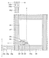
도면에 도시된 바와 같이, 본 발명의 제 1 실시예에 따른 어레이 기판(110)에는 상기 어레이 기판(110) 위에 종횡으로 배열되어 화소영역을 정의하는 게이트라인(116)과 데이터라인(117, 117')이 형성되어 있다. 또한, 상기 게이트라인(116)과 데이터라인(117, 117')의 교차영역에는 스위칭소자인 박막 트랜지스터가 형성되어 있으며, 상기 화소영역 내에는 상기 박막 트랜지스터에 연결되어 컬러필터 기판(미도시)의 공통전극과 함께 액정층(미도시)을 구동시키는 화소전극(118)이 형성되어 있다.As shown in the figure, the
이때, 상기 본 발명의 제 1 실시예에 따른 산화물 박막 트랜지스터는 상기 어레이 기판(110) 위에 형성된 게이트전극(121), 상기 게이트전극(121) 위에 형성된 게이트절연막(115a), 상기 게이트절연막(115a) 위에 형성된 제 1 데이터 배선(즉, 소오스전극(122)과 제 1 드레인전극(123) 및 제 1 데이터라인(117))과 제 2 데이터 배선(즉, 제 2 드레인전극(123') 및 제 2 데이터라인(117')) 및 상기 소오스전극(122)과 제 1 드레인전극(123) 상부에 산화물 반도체로 형성되어 상기 소오스전극(122)과 제 1 드레인전극(123)에 전기적으로 접속하는 액티브층(124)으로 이루어져 있다.The oxide thin film transistor according to the first embodiment of the present invention includes a
그리고, 상기 본 발명의 제 1 실시예에 따른 산화물 박막 트랜지스터는 상기 액티브층(124)이 형성된 어레이 기판(110) 위에 형성된 보호막(115b) 및 상기 보호막(115b)에 형성된 제 1 콘택홀(140a)을 통해 상기 제 2 드레인전극(123')과 전기적으로 접속하는 화소전극(118)을 포함한다.The oxide thin film transistor according to the first embodiment of the present invention includes a
이때, 상기 게이트전극(121)은 상기 게이트라인(116)에 연결되고 상기 소오스전극(122)의 일부는 일 방향으로 연장되어 상기 제 1 데이터라인(117)에 연결되며, 상기 제 2 데이터라인(117')은 상기 제 1 데이터라인(117)과 실질적으로 동일한 형태로 상기 제 1 데이터라인(117) 위에 형성되어 있다.At this time, the
그리고, 상기 제 2 드레인전극(123')은 상기 제 1 콘택홀(140a)이 형성된 상기 제 1 드레인전극(123') 위에 형성되어 있다.The second drain electrode 123 'is formed on the first drain electrode 123' on which the
여기서, 상기 본 발명의 제 1 실시예에 따른 산화물 박막 트랜지스터는 산화물 반도체를 이용하여 액티브층(124)을 형성함에 따라 높은 이동도와 정전류 테스트 조건을 만족하는 한편 균일한 특성이 확보되어 액정표시장치와 유기전계발광 디스플레이를 포함하는 대면적 디스플레이에 적용 가능한 장점을 가지고 있다.Here, the oxide thin film transistor according to the first embodiment of the present invention satisfies the high mobility and constant current test conditions by forming the
또한, 최근 투명 전자회로에 엄청난 관심과 활동이 집중되고 있는데, 상기 산화물 반도체를 액티브층(124)으로 적용한 산화물 박막 트랜지스터는 높은 이동도를 가지는 한편 저온에서 제작이 가능함에 따라 상기 투명 전자회로에 사용될 수 있는 장점이 있다.In recent years, a great deal of attention and activity have been concentrated on transparent electronic circuits. Since the oxide thin film transistor in which the oxide semiconductor is used as the
또한, 상기 산화물 반도체는 넓은 밴드 갭을 가질 수 있어 높은 색순도를 갖는 UV 발광 다이오드(Light Emitting Diode; LED), 백색 LED와 그밖에 다른 부품들을 제작할 수 있으며, 저온에서 공정이 가능하여 가볍고 유연한 제품을 생산할 수 있는 특징을 가지고 있다.In addition, the oxide semiconductor can have a wide bandgap and can produce a UV light emitting diode (LED), a white LED and other components with high color purity, and can produce a light and flexible product by being processable at a low temperature .
이와 같은 특징을 가진 상기 본 발명의 제 1 실시예에 따른 산화물 박막 트랜지스터는 상기 제 1 데이터 배선, 즉 소오스전극(122)과 제 1 드레인전극(123) 위에 액티브층(124)을 형성함으로써 단채널(short channel)을 구현할 수 있게 된다. 즉, 소오스전극(122)과 제 1 드레인전극(123) 위에 액티브층(124)을 형성함으로써 채널 길이가 상기 소오스전극(122)과 제 1 드레인전극(123) 사이의 거리로 설정될 수 있어 에치 스타퍼의 선 폭으로 채널 길이가 결정되는 기존의 구조에 비해 채널 길이를 짧게 설계할 수 있다.The oxide thin film transistor according to the first embodiment of the present invention having such characteristics can form an
또한, 상기 본 발명의 제 1 실시예에 따른 산화물 박막 트랜지스터는 에치 스타퍼가 제거됨에 따라 한번의 포토공정을 삭제할 수 있으며, 상기 제 1 데이터 배선 및 제 2 데이터 배선은 하프-톤 노광을 이용하여 함께 형성할 수 있어 공정이 단순화되게 된다.In addition, the oxide thin film transistor according to the first embodiment of the present invention can eliminate a single photo process as the etch stopper is removed, and the first data line and the second data line are connected together using a half- So that the process can be simplified.
즉, 산화물 박막 트랜지스터는 기존의 비정질 실리콘 박막 트랜지스터 대비 성능이 우수하나 에치 스타퍼의 추가로 포토공정이 추가되는 단점이 있었다. 그러나, 본 발명의 제 1 실시예에서는 게이트전극(121)과 게이트절연막(115a)을 형성한 후, 이종(異種)의 금속물질로 제 1, 제 2 데이터 배선을 형성하게 되는데, 이때 하프-톤 노광을 이용하여 상기 제 1, 제 2 데이터 배선을 형성한 다음 액티브층(124)을 패터닝함으로써 에치 스타퍼를 생략하고 곧바로 보호막(115b)을 형성할 수 있게 된다. 이때, 하프-톤 노광으로 형성되는 제 1, 제 2 데이터 배선 중 상기 액티브층(124)에 접촉하는 제 1 데이터 배선은 접촉특성이 우수한 금속물질로 형성하고, 나머지 제 2 데이터 배선은 전도도가 우수한 금속물질로 형성함으로써 대면적 산화막 박막 트랜지스터 공정에 활용 가능하게 된다.That is, although the oxide thin film transistor has superior performance compared to the conventional amorphous silicon thin film transistor, there is a disadvantage in that a photo process is added in addition to the etch stopper. However, in the first embodiment of the present invention, after the
이와 같이 구성된 상기 본 발명의 제 1 실시예에 따른 어레이 기판(110)의 가장자리 영역에는 상기 게이트라인(116)과 데이터라인(117, 117')에 각각 전기적으로 접속하는 게이트패드전극(126p)과 데이터패드전극(127p)이 형성되어 있으며, 외부의 구동회로부(미도시)로부터 인가 받은 주사신호와 데이터신호를 각각 상기 게이트라인(116)과 데이터라인(117, 117')에 전달하게 된다.A
즉, 상기 게이트라인(116)과 데이터라인(117, 117')은 구동회로부 쪽으로 연장되어 각각 해당하는 게이트패드라인(116p)과 데이터패드라인(117p')에 연결되며, 상기 게이트패드라인(116p)과 데이터패드라인(117p')은 상기 게이트패드라인(116p)과 데이터패드라인(117p')에 각각 전기적으로 접속된 게이트패드전극(126p)과 데이터패드전극(127p)을 통해 구동회로부로부터 각각 주사신호와 데이터신호를 인가 받게 된다.That is, the
이때, 상기 데이터패드라인(117p')은 제 2 콘택홀(140b)을 통해 상기 데이터패드전극(127p)과 전기적으로 접속하게 되며, 상기 게이트패드라인(116p)은 제 3 콘택홀(140c)을 통해 상기 게이트패드전극(126p)과 전기적으로 접속하게 된다. At this time, the
도 6a 내지 도 6e는 상기 도 5에 도시된 본 발명의 제 1 실시예에 따른 어레이 기판의 제조공정을 순차적으로 나타내는 평면도이다.FIGS. 6A to 6E are plan views sequentially illustrating the manufacturing steps of the array substrate according to the first embodiment of the present invention shown in FIG.
또한, 도 7a 내지 도 7e는 상기 도 5에 도시된 본 발명의 제 1 실시예에 따른 어레이 기판의 제조공정을 순차적으로 나타내는 단면도로써, 좌측에는 화소부의 어레이 기판을 제조하는 공정을 나타내며 우측에는 차례대로 데이터패드부와 게이트패드부의 어레이 기판을 제조하는 공정을 나타내고 있다.7A to 7E are cross-sectional views sequentially showing the manufacturing steps of the array substrate according to the first embodiment of the present invention shown in FIG. 5. FIG. 7A to FIG. 7E show the steps of manufacturing the array substrate of the pixel portion on the left side, And a step of manufacturing an array substrate of the data pad portion and the gate pad portion.
도 6a 및 도 7a에 도시된 바와 같이, 투명한 절연물질로 이루어진 어레이 기판(110)의 화소부에 게이트전극(121)과 게이트라인(116)을 형성하며, 상기 어레이 기판(110)의 게이트패드부에 게이트패드라인(116p)을 형성한다.6A and 7A, a
이때, 본 발명의 산화물 박막 트랜지스터에 적용되는 산화물 반도체는 저온 증착이 가능하여, 플라스틱 기판, 소다라임 글라스 등의 저온 공정에 적용이 가능한 기판을 사용할 수 있다. 또한, 비정질 특성을 나타냄으로 인해 대면적 디스플레이용 기판의 사용이 가능하다.At this time, the oxide semiconductor to be applied to the oxide thin film transistor of the present invention can be used for a low-temperature process such as a plastic substrate and a soda lime glass, which can be deposited at a low temperature. In addition, since it exhibits amorphous characteristics, it is possible to use a substrate for a large-area display.
또한, 상기 게이트전극(121)과 게이트라인(116) 및 게이트패드라인(116p)은 제 1 도전막을 상기 어레이 기판(110) 전면에 증착한 후 포토공정을 통해 선택적으로 패터닝하여 형성하게 된다.The
여기서, 상기 제 1 도전막은 알루미늄(aluminium; Al), 알루미늄 합금(Al alloy), 텅스텐(tungsten; W), 구리(copper; Cu), 니켈(nickel; Ni), 크롬(chromium; Cr), 몰리브덴(molybdenum; Mo), 몰리브덴 합금(Mo alloy), 티타늄(titanium; Ti), 백금(platinum; Pt), 탄탈(tantalum; Ta) 등과 같은 저저항 불투명 도전물질로 형성할 수 있다. 또한, 상기 제 1 도전막은 인듐-틴-옥사이드(Indium Tin Oxide; ITO), 인듐-징크-옥사이드(Indium Zinc Oxide; IZO)와 같은 투명한 도전물질로 형성할 수 있으며, 상기 도전물질이 2가지 이상 적층된 다층구조로 형성할 수 있다.The first conductive layer may be formed of one selected from the group consisting of aluminum (Al), aluminum alloy (Al alloy), tungsten (W), copper (Cu), nickel (Ni), chromium (Cr) resistance opaque conductive material such as molybdenum (Mo), molybdenum alloy (Mo), titanium (Ti), platinum (Pt), tantalum (Ta) The first conductive layer may be formed of a transparent conductive material such as indium tin oxide (ITO), indium zinc oxide (IZO), or the like. A multilayered structure can be formed.
다음으로, 도 6b 및 도 7b에 도시된 바와 같이, 상기 게이트전극(121)과 게이트라인(116) 및 게이트패드라인(116p)이 형성된 어레이 기판(110) 전면에 차례대로 게이트절연막(115a)과 제 2 도전막 및 제 3 도전막을 형성한 후, 포토공정을 통해 상기 제 2 도전막 및 제 3 도전막을 선택적으로 패터닝함으로써 상기 어레이 기판(110)에 각각 상기 제 2 도전막 및 제 3 도전막으로 이루어진 제 1 데이터 배선 및 제 2 데이터 배선을 형성한다.Next, as shown in FIGS. 6B and 7B, on the entire surface of the
즉, 포토공정을 통해 상기 제 2 도전막을 선택적으로 패터닝함으로써 상기 어레이 기판(110)의 화소부에 상기 제 2 도전막으로 이루어진 소오스전극(122)과 제 1 드레인전극(123) 및 제 1 데이터라인(117)을 형성하며, 상기 어레이 기판(110)의 데이터패드부에 상기 제 2 도전막으로 이루어진 제 1 데이터패드라인(117p)을 형성한다(제 1 데이터 배선 형성).In other words, by selectively patterning the second conductive layer through a photo process, the
또한, 상기 포토공정을 통해 상기 제 3 도전막을 선택적으로 패터닝함으로써 상기 제 1 드레인전극(123)과 제 1 데이터라인(117) 및 제 1 데이터패드라인(117p) 상부에 상기 제 3 도전막으로 이루어진 제 2 드레인전극(123')과 제 2 데이터라인(117') 및 제 2 데이터패드라인(117p')을 형성하게 된다(제 2 데이터 배선 형성).In addition, the third conductive film is selectively patterned through the photo process to form the third conductive film on the
이때, 상기 소오스전극(122)의 일부는 일 방향으로 연장되어 상기 제 1 데이터라인(117)에 연결되며, 상기 제 2 데이터라인(117')은 상기 제 1 데이터라인(117)과 실질적으로 동일한 형태로 상기 제 1 데이터라인(117) 위에 형성되어 있다. 그리고, 상기 제 2 드레인전극(123')은 화소영역으로 연장된 상기 제 1 드레인전극(123')의 연장부 위에 형성되어 있다.In this case, a part of the
여기서, 상기 제 1 데이터 배선 및 제 2 데이터 배선은 하프-톤 노광을 이용함으로써 한번의 포토공정을 통해 형성할 수 있게 되는데, 이를 다음의 도면을 참조하여 상세히 설명한다.Here, the first data line and the second data line can be formed through a single photo process by using half-tone exposure, which will be described in detail with reference to the following drawings.
도 8a 내지 도 8f는 상기 도 6b 및 도 7b에 도시된 제 2 포토공정을 구체적으로 나타내는 단면도이다.8A to 8F are cross-sectional views illustrating the second photolithography process shown in FIGS. 6B and 7B.
도 8a에 도시된 바와 같이, 상기 게이트전극(121)과 게이트라인(116) 및 게이트패드라인(116p)이 형성된 어레이 기판(110) 전면에 차례대로 게이트절연막(115a)과 제 2 도전막(120) 및 제 3 도전막(130)을 형성한다.A
이때, 상기 게이트절연막(115a)은 실리콘질화막(SiNx), 실리콘산화막(SiO2)과 같은 무기절연막 또는 하프늄(hafnium; Hf) 옥사이드, 알루미늄 옥사이드와 같은 고유전성 산화막으로 형성할 수 있다.In this case, the gate insulating film (115a) is a silicon nitride (SiNx), silicon oxide (SiO 2) or an inorganic insulating film such as a hafnium; can be formed by a highly dielectric oxide film, such as (hafnium Hf) oxide, aluminum oxide.
그리고, 상기 제 2 도전막(120)은 제 1 데이터 배선을 형성하기 위해 액티브층 및 게이트절연막(115a)과의 접촉특성이 우수하고 상기 액티브층과 오믹-콘택이 우수한 몰리브덴 티타늄(MoTi), 인듐-틴-옥사이드(Indium Tin Oxide; ITO), 티타늄 또는 몰리브덴 등의 금속물질로 형성할 수 있다. 그리고, 상기 제 3 도전막(130)은 상기 제 2 도전막(120)과 이종의 금속물질로 상기 제 2 데이터 배선을 형성하기 위해 전도도가 우수한 알루미늄, 구리, 은(Ag), 금(Au) 등의 금속물질로 형성할 수 있다.The second
다음으로, 도 8b에 도시된 바와 같이, 상기 제 3 도전막(130)이 형성된 어레이 기판(110) 위에 포토레지스트와 같은 감광성물질로 이루어진 감광막(160)을 형성한 후 본 발명의 실시예에 따른 하프-톤 마스크(170)를 통해 상기 감광막(160)에 선택적으로 광을 조사한다.8B, a
이때, 상기 하프-톤 마스크(170)에는 조사된 광을 모두 투과시키는 제 1 투과영역(I)과 광의 일부만 투과시키고 일부는 차단하는 제 2 투과영역(II) 및 조사된 모든 광을 차단하는 차단영역(III)이 마련되어 있으며, 상기 하프-톤 마스크(170)를 투과한 광만이 상기 감광막(160)에 조사되게 된다.At this time, the half-
이어서, 상기 하프-톤 마스크(170)를 통해 노광된 상기 감광막(160)을 현상하고 나면, 도 8c에 도시된 바와 같이, 상기 차단영역(III)과 제 2 투과영역(II)을 통해 광이 모두 차단되거나 일부만 차단된 영역에는 소정 두께의 제 1 감광막패턴(160a) 내지 제 5 감광막패턴(160e)이 남아있게 되고, 모든 광이 투과된 제 1 투과영역(I)에는 상기 감광막이 완전히 제거되어 상기 제 3 도전막(130) 표면이 노출되게 된다.Then, after the
이때, 상기 차단영역(III)에 형성된 제 1 감광막패턴(160a)은 제 2 투과영역(II)을 통해 형성된 제 2 감광막패턴(160b) 내지 제 5 감광막패턴(160e)보다 두껍게 형성된다. 또한, 상기 제 1 투과영역(I)을 통해 광이 모두 투과된 영역에는 감광막이 완전히 제거되는데, 이것은 포지티브 타입의 포토레지스트를 사용했기 때문이며, 본 발명이 이에 한정되는 것은 아니며 네거티브 타입의 포토레지스트를 사용하여도 무방하다.The
다음으로, 도 8d에 도시된 바와 같이, 상기와 같이 형성된 제 1 감광막패턴(160a) 내지 제 5 감광막패턴(160e)을 마스크로 하여, 그 하부에 형성된 제 2 도전막과 제 3 도전막의 일부영역을 선택적으로 제거하게 되면, 상기 어레이 기판(110)의 화소부에 상기 제 2 도전막으로 이루어진 소오스전극(122)과 제 1 드레인전극(123) 및 제 1 데이터라인(117)이 형성된다.Next, as shown in FIG. 8D, using the
또한, 상기 어레이 기판(110)의 데이터패드부에 상기 제 2 도전막으로 이루어진 제 1 데이터패드라인(117p)이 형성되게 된다.In addition, a first
이때, 상기 소오스전극(122)과 제 1 데이터라인(117) 및 제 1 드레인전극(123) 위에는 상기 제 3 도전막으로 이루어진 도전막패턴(130', 130")이 형성되어 있으며, 상기 제 1 데이터패드라인(117p) 위에는 상기 제 3 도전막으로 이루어진 제 2 데이터패드라인(117')이 형성되어 있다.At this time,
이후, 상기 제 1 감광막패턴(160a) 내지 제 5 감광막패턴(160e)의 두께 일부를 제거하는 애싱공정을 진행하게 되면, 도 8e에 도시된 바와 같이, 상기 제 2 투과영역(II)의 제 4 감광막패턴 및 제 5 감광막패턴이 완전히 제거되게 된다.As shown in FIG. 8E, when the ashing process for removing a part of the thicknesses of the first to
이때, 상기 제 1 감광막패턴 내지 제 3 감광막패턴은 상기 제 4 감광막패턴 및 제 5 감광막패턴의 두께만큼이 제거된 제 6 감광막패턴(160a') 내지 제 8 감광막패턴(160c')으로 상기 차단영역(III)에 대응하는 영역에만 남아있게 된다.In this case, the first to third photoresist patterns to the
이후, 도 8f에 도시된 바와 같이, 상기 제 6 감광막패턴(160a') 내지 제 8 감광막패턴(160c')을 마스크로 하여, 그 하부에 형성된 도전막패턴의 일부영역을 선택적으로 제거하게 되면, 상기 제 1 드레인전극(123) 및 제 1 데이터라인(117) 상부에 상기 제 3 도전막으로 이루어진 제 2 드레인전극(123') 및 제 2 데이터라인(117')이 각각 형성되게 된다.Then, as shown in FIG. 8F, using the
이때, 전술한 바와 같이 상기 제 2 데이터라인(117')은 상기 제 1 데이터라인(117)과 실질적으로 동일한 형태로 상기 제 1 데이터라인(117) 위에 형성될 수 있으며, 상기 제 2 드레인전극(123')은 화소영역으로 연장된 상기 제 1 드레인전극(123')의 연장부 위에 형성될 수 있다.At this time, as described above, the second data line 117 'may be formed on the
다음으로, 도 6c 및 도 7c에 도시된 바와 같이, 상기 제 1 데이터 배선 및 제 2 데이터 배선이 형성된 어레이 기판(110) 전면에 소정의 산화물 반도체로 이루어진 산화물 반도체층을 형성한 후, 포토공정을 통해 상기 산화물 반도체층을 선택적으로 패터닝하게 되면, 상기 어레이 기판(110)의 소오스전극(122) 및 제 1 드레인전극(123) 상부에 상기 산화물 반도체로 이루어진 액티브층(124)이 형성되게 된다.Next, as shown in FIGS. 6C and 7C, an oxide semiconductor layer made of a predetermined oxide semiconductor is formed on the entire surface of the
이때, 상기 액티브층(124)은 상기 제 2 데이터라인(117')과 제 2 드레인전극(123') 사이에 위치하는 아일랜드 형태로 형성되게 된다.At this time, the
이와 같이 상기 본 발명의 제 1 실시예에 따른 산화물 박막 트랜지스터는 에치 스타퍼를 제거함에 따라 기존의 에치 스타퍼 구조 대비 한번의 포토공정을 줄일 수 있으며, 제 1 데이터 배선, 즉 소오스전극(122)과 제 1 드레인전극(123)에 의해 채널 길이를 결정할 수 있어 4㎛ ~ 10㎛정도의 단채널을 구현할 수 있는 특징을 가진다.As described above, the oxide thin film transistor according to the first embodiment of the present invention can reduce a single photo process compared to the conventional etch stop structure by removing the etch stopper, and the first data line, that is, the
다음으로, 도 6d 및 도 7d에 도시된 바와 같이, 상기 액티브층(124)이 형성된 어레이 기판(110) 전면에 소정의 절연물질로 이루어진 보호막(115b)을 형성한다.Next, as shown in FIGS. 6D and 7D, a
이후, 포토공정을 통해 상기 게이트절연막(115a)과 보호막(115b)을 선택적으로 제거하게 되면, 상기 어레이 기판(110)의 화소부에 상기 제 2 드레인전극(123')의 일부를 노출시키는 제 1 콘택홀(140a)이 형성되며, 상기 어레이 기판(110)의 데이터패드부 및 게이트패드부에 각각 상기 제 2 데이터패드라인(117p') 및 게이트패드라인(116p)의 일부를 노출시키는 제 2 콘택홀(140b) 및 제 3 콘택홀(140c)이 형성되게 된다.Thereafter, the
이때, 상기 보호막(115b)은 실리콘질화막, 실리콘산화막과 같은 무기절연막 또는 하프늄 옥사이드, 알루미늄 옥사이드와 같은 고유전성 산화막으로 형성할 수 있다.At this time, the
한편, 상기 제 2 데이터 배선의 부식 영향에 따라 상기 액티브층(124)의 형성 중, 예를 들어 산화물 반도체층의 형성 후 또는 상기 보호막(115b)의 형성 후에 소정의 열처리공정을 진행할 수 있다.Meanwhile, a predetermined heat treatment process may be performed during the formation of the
다음으로, 도 6e 및 도 7e에 도시된 바와 같이, 상기 보호막(115b)이 형성된 어레이 기판(110) 전면에 제 4 도전막을 형성한 후, 포토공정을 통해 선택적으로 제거함으로써 상기 어레이 기판(110)의 화소부에 상기 제 4 도전막으로 이루어지며, 상기 제 1 콘택홀(140a)을 통해 상기 제 2 드레인전극(123')과 전기적으로 접속하는 화소전극(118)을 형성한다.6E and 7E, a fourth conductive layer is formed on the entire surface of the
또한, 상기 포토공정을 통해 상기 어레이 기판의 기판(110)의 데이터패드부 및 게이트패드부에 상기 제 4 도전막으로 일어지며, 각각 상기 제 2 콘택홀(140b) 및 제 3 콘택홀(140c)을 통해 상기 제 2 데이터패드라인(117p') 및 게이트패드라인(116p)과 전기적으로 접속하는 데이터패드전극(127p) 및 게이트패드전극(126p)을 형성하게 된다.In addition, the fourth conductive film is formed on the data pad portion and the gate pad portion of the
이때, 상기 제 4 도전막은 상기 화소전극(118)과 데이터패드전극(127p) 및 게이트패드전극(126p)을 구성하기 위해 인듐-틴-옥사이드 또는 인듐-징크-옥사이드와 같은 투과율이 뛰어난 투명한 도전물질로 형성할 수 있다.The fourth conductive layer may be a transparent conductive material having a high transmittance such as indium-tin-oxide or indium-zinc-oxide for forming the
전술한 바와 같이 본 발명의 제 1 실시예에 따른 산화물 박막 트랜지스터는 4㎛ ~ 10㎛의 단채널을 구현함에 따라 온 전류의 향상, 기생 커패시턴스의 감소 등 대면적 산화물 박막 트랜지스터의 성능을 향상시킬 수 있다. 또한, 본 발명의 제 1 실시예에 따른 산화물 박막 트랜지스터는 에치 스타퍼를 제거할 수 있어 포토공정의 삭제로 공정이 단순화되게 된다.As described above, the oxide thin film transistor according to the first embodiment of the present invention realizes a short channel of 4 탆 to 10 탆, thereby improving the performance of the large-area oxide thin film transistor, such as the improvement of the ON current and the reduction of the parasitic capacitance have. Also, since the oxide thin film transistor according to the first embodiment of the present invention can remove the etch stopper, the process can be simplified by eliminating the photo process.
한편, 본 발명은 액티브층 상, 하부에 소오스/드레인전극을 형성하여 액티브층과의 접촉 면적을 증가시킬 수 있으며, 이 경우 오믹-콘택의 개선으로 소자 특성이 향상되게 되는데, 이를 다음의 제 2 실시예를 통해 상세히 설명한다.Meanwhile, the present invention can increase the contact area with the active layer by forming source / drain electrodes on and under the active layer. In this case, improvement of the ohmic contact improves the device characteristics. The embodiment will be described in detail.
도 9는 본 발명의 제 2 실시예에 따른 산화물 박막 트랜지스터를 개략적으로 나타내는 단면도이다.9 is a cross-sectional view schematically showing an oxide thin film transistor according to a second embodiment of the present invention.
또한, 도 10은 본 발명의 제 2 실시예에 따른 액정표시장치의 어레이 기판 일부를 개략적으로 나타내는 평면도이다.10 is a plan view schematically showing a part of an array substrate of a liquid crystal display device according to a second embodiment of the present invention.
이때, 실제의 액정표시장치에서는 N개의 게이트라인과 M개의 데이터라인이 교차하여 MxN개의 화소가 존재하지만 설명을 간단하게 하기 위해 도면에는 하나의 화소를 나타내고 있다.At this time, in an actual liquid crystal display device, N number of gate lines and M number of data lines intersect to form MxN pixels, but one pixel is shown in the drawing for simplicity of explanation.
도면에 도시된 바와 같이, 본 발명의 제 2 실시예에 따른 어레이 기판(210)에는 상기 어레이 기판(210) 위에 종횡으로 배열되어 화소영역을 정의하는 게이트라인(216)과 데이터라인(217, 217')이 형성되어 있다. 또한, 상기 게이트라인(216)과 데이터라인(217, 217')의 교차영역에는 스위칭소자인 박막 트랜지스터가 형성되어 있으며, 상기 화소영역 내에는 상기 박막 트랜지스터에 연결되어 컬러필터 기판(미도시)의 공통전극과 함께 액정층(미도시)을 구동시키는 화소전극(218)이 형성되어 있다.As shown in the figure, the
이때, 상기 본 발명의 제 2 실시예에 따른 산화물 박막 트랜지스터는 상기 어레이 기판(210) 위에 형성된 게이트전극(221), 상기 게이트전극(221) 위에 형성된 게이트절연막(215a), 상기 게이트절연막(215a) 위에 형성된 제 1 데이터 배선(즉, 제 1 소오스전극(222)과 제 1 드레인전극(223) 및 제 1 데이터라인(217)), 상기 제 1 소오스전극(222)과 제 1 드레인전극(223) 상부에 산화물 반도체로 형성되어 상기 제 1 소오스전극(222)과 제 1 드레인전극(223)에 전기적으로 접속하는 액티브층(224), 상기 액티브층(224) 상부에 형성된 에치 스타퍼(225) 및 제 2 데이터 배선(즉, 제 2 소오스전극(222')과 제 2 드레인전극(223') 및 제 2 데이터라인(217'))으로 이루어져 있다.The oxide thin film transistor according to the second embodiment of the present invention includes a
그리고, 상기 본 발명의 제 2 실시예에 따른 산화물 박막 트랜지스터는 상기 액티브층(224)이 형성된 어레이 기판(210) 위에 형성된 보호막(215b) 및 상기 보호막(215b)에 형성된 제 1 콘택홀(240a)을 통해 상기 제 2 드레인전극(223')과 전기적으로 접속하는 화소전극(218)을 포함한다.The oxide thin film transistor according to the second embodiment of the present invention includes a
이때, 상기 게이트전극(221)은 상기 게이트라인(216)에 연결되고 상기 제 1 소오스전극(222) 및 제 2 소오스전극(222')의 일부는 일 방향으로 연장되어 각각 상기 제 1 데이터라인(217) 및 제 2 데이터라인(217')에 연결되며, 상기 제 2 데이터라인(217')은 상기 제 1 데이터라인(217)과 실질적으로 동일한 형태로 상기 제 1 데이터라인(217) 위에 형성될 수 있다.At this time, the
여기서, 상기 본 발명의 제 2 실시예에 따른 산화물 박막 트랜지스터는 전술한 본 발명의 제 1 실시예와 동일하게 산화물 반도체를 이용하여 액티브층(224)을 형성함에 따라 높은 이동도와 정전류 테스트 조건을 만족하는 한편 균일한 특성이 확보되어 액정표시장치와 유기전계발광 디스플레이를 포함하는 대면적 디스플레이에 적용 가능한 장점을 가지고 있다.In the oxide thin film transistor according to the second embodiment of the present invention, the
또한, 최근 투명 전자회로에 엄청난 관심과 활동이 집중되고 있는데, 상기 산화물 반도체를 액티브층(224)으로 적용한 산화물 박막 트랜지스터는 높은 이동도를 가지는 한편 저온에서 제작이 가능함에 따라 상기 투명 전자회로에 사용될 수 있는 장점이 있다.In recent years, a great deal of attention and activity have been concentrated on transparent electronic circuits. Since oxide thin film transistors using the oxide semiconductor as the
또한, 상기 산화물 반도체는 넓은 밴드 갭을 가질 수 있어 높은 색순도를 갖는 UV LED, 백색 LED와 그밖에 다른 부품들을 제작할 수 있으며, 저온에서 공정이 가능하여 가볍고 유연한 제품을 생산할 수 있는 특징을 가지고 있다.In addition, the oxide semiconductor can have a wide band gap, and can produce a UV LED, a white LED, and other components having high color purity, and can produce a light and flexible product because it can be processed at a low temperature.
또한, 상기 본 발명의 제 2 실시예에 따른 산화물 박막 트랜지스터는 상기 제 1 데이터 배선, 즉 제 1 소오스전극(222)과 제 1 드레인전극(223) 위에 액티브층(224)을 형성함으로써 단채널을 구현할 수 있게 된다. 즉, 제 1 소오스전극(222)과 제 1 드레인전극(223) 위에 액티브층(224)을 형성함으로써 채널 길이가 상기 소오스전극(222)과 제 1 드레인전극(223) 사이의 거리로 설정될 수 있어 에치 스타퍼의 선 폭으로 채널 길이가 결정되는 기존의 구조에 비해 채널 길이를 짧게 설계할 수 있다.In the oxide thin film transistor according to the second embodiment of the present invention, an
또한, 상기 본 발명의 제 2 실시예에 따른 산화물 박막 트랜지스터는 액티브층(224) 상, 하부에 소오스/드레인전극(222,222', 223,223')을 형성함에 따라 액티브층(224)과의 접촉 면적을 증가시킬 수 있으며, 이 경우 오믹-콘택의 개선으로 소자 특성이 향상되게 된다.In the oxide thin film transistor according to the second embodiment of the present invention, since the source /
이와 같이 구성된 상기 본 발명의 제 2 실시예에 따른 어레이 기판(210)의 가장자리 영역에는 상기 게이트라인(216)과 데이터라인(217, 217')에 각각 전기적으로 접속하는 게이트패드전극(226p)과 데이터패드전극(227p)이 형성되어 있으며, 외부의 구동회로부(미도시)로부터 인가 받은 주사신호와 데이터신호를 각각 상기 게이트라인(216)과 데이터라인(217, 217')에 전달하게 된다.A
즉, 상기 게이트라인(216)과 데이터라인(217, 217')은 구동회로부 쪽으로 연장되어 각각 해당하는 게이트패드라인(216p)과 데이터패드라인(217p')에 연결되며, 상기 게이트패드라인(216p)과 데이터패드라인(217p')은 상기 게이트패드라인(216p)과 데이터패드라인(217p')에 각각 전기적으로 접속된 게이트패드전극(226p)과 데이터패드전극(227p)을 통해 구동회로부로부터 각각 주사신호와 데이터신호를 인가 받게 된다.That is, the
이때, 상기 데이터패드라인(217p')은 제 2 콘택홀(240b)을 통해 상기 데이터패드전극(227p)과 전기적으로 접속하게 되며, 상기 게이트패드라인(216p)은 제 3 콘택홀(240c)을 통해 상기 게이트패드전극(226p)과 전기적으로 접속하게 된다.At this time, the
도 11a 내지 도 11f는 상기 도 10에 도시된 본 발명의 제 2 실시예에 따른 어레이 기판의 제조공정을 순차적으로 나타내는 평면도이다.FIGS. 11A to 11F are plan views sequentially illustrating the manufacturing steps of the array substrate according to the second embodiment of the present invention shown in FIG.
또한, 도 12a 내지 도 12f는 상기 도 10에 도시된 본 발명의 제 2 실시예에 따른 어레이 기판의 제조공정을 순차적으로 나타내는 단면도로써, 좌측에는 화소부의 어레이 기판을 제조하는 공정을 나타내며 우측에는 차례대로 데이터패드부와 게이트패드부의 어레이 기판을 제조하는 공정을 나타내고 있다.12A to 12F are cross-sectional views sequentially showing the manufacturing steps of the array substrate according to the second embodiment of the present invention shown in FIG. 10, wherein the left side shows the step of manufacturing the array substrate of the pixel portion, And a step of manufacturing an array substrate of the data pad portion and the gate pad portion.
도 11a 및 도 12a에 도시된 바와 같이, 투명한 절연물질로 이루어진 어레이 기판(210)의 화소부에 게이트전극(221)과 게이트라인(216)을 형성하며, 상기 어레이 기판(210)의 게이트패드부에 게이트패드라인(216p)을 형성한다.A
이때, 본 발명의 산화물 박막 트랜지스터에 적용되는 산화물 반도체는 저온 증착이 가능하여, 플라스틱 기판, 소다라임 글라스 등의 저온 공정에 적용이 가능한 기판을 사용할 수 있다. 또한, 비정질 특성을 나타냄으로 인해 대면적 디스플레이용 기판의 사용이 가능하다.At this time, the oxide semiconductor to be applied to the oxide thin film transistor of the present invention can be used for a low-temperature process such as a plastic substrate and a soda lime glass, which can be deposited at a low temperature. In addition, since it exhibits amorphous characteristics, it is possible to use a substrate for a large-area display.
또한, 상기 게이트전극(221)과 게이트라인(216) 및 게이트패드라인(216p)은 제 1 도전막을 상기 어레이 기판(210) 전면에 증착한 후 포토공정을 통해 선택적으로 패터닝하여 형성하게 된다.The
여기서, 상기 제 1 도전막은 알루미늄, 알루미늄 합금, 텅스텐, 구리, 니켈, 크롬, 몰리브덴, 몰리브덴 합금, 티타늄, 백금, 탄탈 등과 같은 저저항 불투명 도전물질로 형성할 수 있다. 또한, 상기 제 1 도전막은 인듐-틴-옥사이드, 인듐-징크-옥사이드와 같은 투명한 도전물질로 형성할 수 있으며, 상기 도전물질이 2가지 이상 적층된 다층구조로 형성할 수 있다.The first conductive layer may be formed of a low-resistance opaque conductive material such as aluminum, an aluminum alloy, tungsten, copper, nickel, chromium, molybdenum, molybdenum alloy, titanium, platinum or tantalum. Also, the first conductive layer may be formed of a transparent conductive material such as indium-tin-oxide or indium-zinc-oxide, or may have a multi-layer structure in which two or more conductive materials are stacked.
다음으로, 도 11b 및 도 12b에 도시된 바와 같이, 상기 게이트전극(221)과 게이트라인(216) 및 게이트패드라인(216p)이 형성된 어레이 기판(210) 전면에 차례대로 게이트절연막(215a)과 제 2 도전막을 형성한다.Next, as shown in FIGS. 11B and 12B, on the entire surface of the
이후, 포토공정을 통해 상기 제 2 도전막을 선택적으로 패터닝함으로써 상기 어레이 기판(210)의 화소부에 상기 제 2 도전막으로 이루어진 제 1 소오스전극(222)과 제 1 드레인전극(223) 및 제 1 데이터라인(217)을 형성하며, 상기 어레이 기판(210)의 데이터패드부에 상기 제 2 도전막으로 이루어진 제 1 데이터패드라인(217p)을 형성한다(제 1 데이터 배선 형성).Thereafter, the second conductive film is selectively patterned through a photo process to form a
이때, 상기 게이트절연막(215a)은 실리콘질화막, 실리콘산화막과 같은 무기절연막 또는 하프늄 옥사이드, 알루미늄 옥사이드와 같은 고유전성 산화막으로 형성할 수 있다.At this time, the
또한, 상기 제 2 도전막은 상기 제 1 데이터 배선을 형성하기 위해 액티브층 및 게이트절연막(215a)과의 접촉특성이 우수하고 상기 액티브층과 오믹-콘택이 우수한 몰리브덴 티타늄, 인듐-틴-옥사이드, 티타늄 또는 몰리브덴 등의 금속물질로 형성할 수 있다.In addition, the second conductive layer may be formed of at least one selected from the group consisting of molybdenum titanium, indium-tin-oxide, titanium oxide, and tantalum oxide, which have excellent contact properties with the active layer and the
이때, 상기 제 1 소오스전극(222)의 일부는 일 방향으로 연장되어 상기 제 1 데이터라인(217)에 연결된다.At this time, a part of the
다음으로, 도 11c 및 도 12c에 도시된 바와 같이, 상기 제 1 데이터 배선이 형성된 어레이 기판(210) 전면에 소정의 산화물 반도체로 이루어진 산화물 반도체층 및 절연층을 형성한 후, 포토공정을 통해 상기 산화물 반도체층 및 절연층을 선택적으로 패터닝하게 되면, 상기 어레이 기판(210)의 제 1 소오스전극(222) 및 제 1 드레인전극(223) 상부에 상기 산화물 반도체로 이루어진 액티브층(224)이 형성되게 되며, 상기 액티브층(224) 위에 상기 절연층으로 이루어진 에치 스타퍼(225)가 형성되게 된다.Next, as shown in FIGS. 11C and 12C, an oxide semiconductor layer made of a predetermined oxide semiconductor and an insulating layer are formed on the entire surface of the
이때, 상기 액티브층(224)은 상기 제 1 소오스전극(222) 및 제 1 드레인전극(223) 상부에 아일랜드 형태로 형성되며, 하프-톤 노광을 이용할 경우 상기 에치 스타퍼(225)와 동일한 포토공정을 통해 형성할 수 있게 된다.At this time, the
다음으로, 도 11d 및 도 12d에 도시된 바와 같이, 상기 액티브층(224)이 형성된 어레이 기판(210) 전면에 제 3 도전막을 형성한다.Next, as shown in FIGS. 11D and 12D, a third conductive film is formed on the entire surface of the
이때, 상기 제 3 도전막은 상기 제 2 도전막과 이종의 금속물질로 형성할 수도 있으며, 이 경우 제 2 데이터 배선을 형성하기 위해 전도도가 우수한 알루미늄, 구리, 은, 금 등의 금속물질로 형성할 수 있다. 다만, 본 발명이 이에 한정되는 것은 아니다.The third conductive layer may be formed of a different metal material from the second conductive layer. In this case, the third conductive layer may be formed of a metal material such as aluminum, copper, silver, gold, or the like, . However, the present invention is not limited thereto.
이후, 포토공정을 통해 상기 제 3 도전막을 선택적으로 제거함으로써 상기 액티브층(224) 및 에치 스타퍼(225) 상부에 상기 제 3 도전막으로 이루어진 제 2 소오스전극(222')과 제 2 드레인전극(223') 및 제 2 데이터라인(217')을 형성하며, 상기 제 1 데이터패드라인(217p) 위에 상기 제 3 도전막으로 이루어진 제 2 데이터패드라인(217p')을 형성하게 된다(제 2 데이터 배선 형성).Thereafter, the third conductive film is selectively removed through a photolithography process so that a second source electrode 222 'and a second drain electrode 222', which are made of the third conductive film, are formed on the
이때, 상기 제 2 소오스전극(222')의 일부는 일 방향으로 연장되어 상기 제 2 데이터라인(217')에 연결되며, 상기 제 2 데이터라인(217')은 상기 제 1 데이터라인(217)과 실질적으로 동일한 형태로 상기 제 1 데이터라인(217) 위에 형성될 수 있다.In this case, a part of the second source electrode 222 'extends in one direction and is connected to the second data line 217', and the second data line 217 'is connected to the first data line 217' May be formed on the
다음으로, 도 11e 및 도 12e에 도시된 바와 같이, 상기 액티브층(224)이 형성된 어레이 기판(210) 전면에 소정의 절연물질로 이루어진 보호막(215b)을 형성한다.Next, as shown in FIGS. 11E and 12E, a
이후, 포토공정을 통해 상기 게이트절연막(215a)과 보호막(215b)을 선택적으로 제거하게 되면, 상기 어레이 기판(210)의 화소부에 상기 제 2 드레인전극(223')의 일부를 노출시키는 제 1 콘택홀(240a)이 형성되며, 상기 어레이 기판(210)의 데이터패드부 및 게이트패드부에 각각 상기 제 2 데이터패드라인(217p') 및 게이트패드라인(216p)의 일부를 노출시키는 제 2 콘택홀(240b) 및 제 3 콘택홀(240c)이 형성되게 된다.Thereafter, when the
이때, 상기 보호막(215b)은 실리콘질화막, 실리콘산화막과 같은 무기절연막 또는 하프늄 옥사이드, 알루미늄 옥사이드와 같은 고유전성 산화막으로 형성할 수 있다.At this time, the
다음으로, 도 11f 및 도 12f에 도시된 바와 같이, 상기 보호막(215b)이 형성된 어레이 기판(210) 전면에 제 4 도전막을 형성한 후, 포토공정을 통해 선택적으로 제거함으로써 상기 어레이 기판(210)의 화소부에 상기 제 4 도전막으로 이루어지며, 상기 제 1 콘택홀(240a)을 통해 상기 제 2 드레인전극(223')과 전기적으로 접속하는 화소전극(218)을 형성한다.Next, as shown in FIGS. 11F and 12F, a fourth conductive film is formed on the entire surface of the
또한, 상기 포토공정을 통해 상기 어레이 기판의 기판(210)의 데이터패드부 및 게이트패드부에 상기 제 4 도전막으로 일어지며, 각각 상기 제 2 콘택홀(240b) 및 제 3 콘택홀(240c)을 통해 상기 제 2 데이터패드라인(217p') 및 게이트패드라인(216p)과 전기적으로 접속하는 데이터패드전극(227p) 및 게이트패드전극(226p)을 형성하게 된다.In addition, the fourth conductive film is formed on the data pad portion and the gate pad portion of the
이때, 상기 제 4 도전막은 상기 화소전극(218)과 데이터패드전극(227p) 및 게이트패드전극(226p)을 구성하기 위해 인듐-틴-옥사이드 또는 인듐-징크-옥사이드와 같은 투과율이 뛰어난 투명한 도전물질로 형성할 수 있다.The fourth conductive layer may be a transparent conductive material having a high transmittance such as indium-tin-oxide or indium-zinc-oxide for forming the
전술한 바와 같이 본 발명은 액정표시장치뿐만 아니라 박막 트랜지스터를 이용하여 제작하는 다른 표시장치, 예를 들면 구동 트랜지스터에 유기전계발광소자가 연결된 유기전계발광 디스플레이장치에도 이용될 수 있다.As described above, the present invention can be applied not only to liquid crystal display devices but also to other display devices manufactured using thin film transistors, for example, organic electroluminescent display devices in which organic electroluminescent devices are connected to driving transistors.
또한, 본 발명은 높은 이동도를 가지는 한편 저온에서 공정이 가능한 비정질 산화물 반도체 물질을 액티브층으로 적용함에 따라 투명 전자회로나 플렉서블(flexible) 디스플레이에 사용될 수 있는 장점이 있다.In addition, the present invention has an advantage that it can be used in a transparent electronic circuit or a flexible display by applying an amorphous oxide semiconductor material having a high mobility and being processable at a low temperature as an active layer.
상기한 설명에 많은 사항이 구체적으로 기재되어 있으나 이것은 발명의 범위를 한정하는 것이라기보다 바람직한 실시예의 예시로서 해석되어야 한다. 따라서 발명은 설명된 실시예에 의하여 정할 것이 아니고 특허청구범위와 특허청구범위에 균등한 것에 의하여 정하여져야 한다.While a great many are described in the foregoing description, it should be construed as an example of preferred embodiments rather than limiting the scope of the invention. Therefore, the invention should not be construed as limited to the embodiments described, but should be determined by equivalents to the appended claims and the claims.
110,210 : 어레이 기판 116,216 : 게이트라인
117,117',217,217' : 데이터라인 118,218 : 화소전극
121,221 : 게이트전극 122,222,222' : 소오스전극
123,123',223,223' : 드레인전극 124,224 : 액티브층
225 : 에치 스타퍼110, 210:
117, 117 ', 217, 217':
121, 221:
123, 123 ', 223, 223':
225: Etch Starper
Claims (15)
상기 게이트전극 및 게이트라인이 형성된 기판 위에 게이트절연막을 형성하는 단계;
하프-톤 노광을 이용하여 상기 게이트절연막이 형성된 게이트전극 상부에 제 2 도전막으로 이루어진 소오스전극과 연장부를 가진 제 1 드레인전극 및 제 1 데이터라인을 형성하는 한편, 상기 제 1 드레인전극의 연장부 및 상기 제 1 데이터라인 위에 제 3 도전막으로 이루어진 제 2 드레인전극 및 제 2 데이터라인을 각각 형성하는 단계;
상기 소오스전극 및 제 1 드레인전극 위에 산화물 반도체로 이루어진 액티브층을 형성하는 단계;
상기 액티브층이 형성된 기판 위에 보호막을 형성하는 단계; 및
상기 보호막 위에 상기 제 2 드레인전극과 전기적으로 접속하는 화소전극을 형성하는 단계를 포함하며,
상기 액티브층과 제 2 드레인전극은 상기 소오스전극 및 제 1 드레인전극이 형성된 기판 위의 동일층에 형성되는 것을 특징으로 하는 산화물 박막 트랜지스터의 제조방법.Forming a gate electrode and a gate line made of a first conductive film on a substrate;
Forming a gate insulating film on the substrate on which the gate electrode and the gate line are formed;
A first drain electrode and a first data line having a source electrode made of a second conductive film and an extended portion and a first data line are formed on the gate electrode on which the gate insulating film is formed by using half-tone exposure, And forming a second drain electrode and a second data line each made of a third conductive film on the first data line;
Forming an active layer made of an oxide semiconductor on the source electrode and the first drain electrode;
Forming a protective film on the substrate on which the active layer is formed; And
And forming a pixel electrode electrically connected to the second drain electrode on the protective film,
Wherein the active layer and the second drain electrode are formed on the same layer on the substrate on which the source electrode and the first drain electrode are formed.
상기 게이트전극 및 게이트라인이 형성된 기판 위에 형성된 게이트절연막;
상기 게이트절연막이 형성된 게이트전극 상부에 제 2 도전막으로 형성된 소오스전극과 연장부를 가진 제 1 드레인전극 및 제 1 데이터라인;
상기 제 1 드레인전극의 연장부 및 상기 제 1 데이터라인 위에 제 3 도전막으로 각각 형성된 제 2 드레인전극 및 제 2 데이터라인;
상기 소오스전극 및 제 1 드레인전극 위에 산화물 반도체로 형성된 액티브층;
상기 액티브층이 형성된 기판 위에 형성된 보호막; 및
상기 보호막 위에 형성되어 상기 제 2 드레인전극과 전기적으로 접속하는 화소전극을 포함하며,
상기 액티브층과 제 2 드레인전극은 상기 소오스전극 및 제 1 드레인전극이 형성된 기판 위의 동일층에 위치하는 것을 특징으로 하는 산화물 박막 트랜지스터.A gate electrode and a gate line formed of a first conductive film on a substrate;
A gate insulating film formed on the substrate on which the gate electrode and the gate line are formed;
A first drain electrode and a first data line having a source electrode and an extended portion formed of a second conductive film over the gate electrode on which the gate insulating film is formed;
A second drain electrode and a second data line respectively formed as an extension of the first drain electrode and a third conductive film on the first data line;
An active layer formed of an oxide semiconductor on the source electrode and the first drain electrode;
A protective film formed on the substrate on which the active layer is formed; And
And a pixel electrode formed on the protective film and electrically connected to the second drain electrode,
Wherein the active layer and the second drain electrode are located on the same layer on the substrate on which the source electrode and the first drain electrode are formed.
Priority Applications (5)
| Application Number | Priority Date | Filing Date | Title |
|---|---|---|---|
| KR1020110055786A KR101425064B1 (en) | 2011-06-09 | 2011-06-09 | Oxide thin film transistor and method of fabricating the same |
| GB1210001.2A GB2492627B (en) | 2011-06-09 | 2012-06-06 | Oxide thin film transistor and method of fabricating the same |
| US13/490,614 US9059296B2 (en) | 2011-06-09 | 2012-06-07 | Oxide thin film transistor and method of fabricating the same |
| CN201210186683.5A CN102820319B (en) | 2011-06-09 | 2012-06-07 | Oxide thin film transistor and manufacture method thereof |
| JP2012130499A JP2012256890A (en) | 2011-06-09 | 2012-06-08 | Oxide thin film transistor and manufacturing method of the same |
Applications Claiming Priority (1)
| Application Number | Priority Date | Filing Date | Title |
|---|---|---|---|
| KR1020110055786A KR101425064B1 (en) | 2011-06-09 | 2011-06-09 | Oxide thin film transistor and method of fabricating the same |
Publications (2)
| Publication Number | Publication Date |
|---|---|
| KR20120136695A KR20120136695A (en) | 2012-12-20 |
| KR101425064B1 true KR101425064B1 (en) | 2014-08-01 |
Family
ID=46582377
Family Applications (1)
| Application Number | Title | Priority Date | Filing Date |
|---|---|---|---|
| KR1020110055786A Active KR101425064B1 (en) | 2011-06-09 | 2011-06-09 | Oxide thin film transistor and method of fabricating the same |
Country Status (5)
| Country | Link |
|---|---|
| US (1) | US9059296B2 (en) |
| JP (1) | JP2012256890A (en) |
| KR (1) | KR101425064B1 (en) |
| CN (1) | CN102820319B (en) |
| GB (1) | GB2492627B (en) |
Families Citing this family (25)
| Publication number | Priority date | Publication date | Assignee | Title |
|---|---|---|---|---|
| JP2012204548A (en) * | 2011-03-24 | 2012-10-22 | Sony Corp | Display device and manufacturing method therefor |
| KR101913207B1 (en) * | 2011-10-12 | 2018-11-01 | 삼성디스플레이 주식회사 | Thin film transistor, thin film transistor panel and method of manufacturing the same |
| WO2013061895A1 (en) * | 2011-10-28 | 2013-05-02 | Semiconductor Energy Laboratory Co., Ltd. | Semiconductor device and manufacturing method thereof |
| KR102028980B1 (en) * | 2013-01-31 | 2019-10-08 | 엘지디스플레이 주식회사 | Method of fabricating thin film transistor substrate |
| CN103984171A (en) * | 2013-02-22 | 2014-08-13 | 上海天马微电子有限公司 | Array substrate, manufacturing method thereof and liquid crystal display |
| JP2014183265A (en) * | 2013-03-21 | 2014-09-29 | Toppan Printing Co Ltd | Thin film transistor array, manufacturing method thereof and image display device |
| US20160004110A1 (en) * | 2013-03-22 | 2016-01-07 | Sharp Kabushiki Kaisha | Display panel and method of producing display panel |
| KR102196949B1 (en) * | 2013-03-29 | 2020-12-30 | 엘지디스플레이 주식회사 | Thin film transistor, method for manufacturing the same and display device comprising the same |
| JP6124668B2 (en) * | 2013-04-26 | 2017-05-10 | 三菱電機株式会社 | Thin film transistor substrate and manufacturing method thereof |
| KR102081107B1 (en) * | 2013-05-30 | 2020-02-25 | 엘지디스플레이 주식회사 | Thin film transistor array substrate and manufacturing method of the same |
| JP6180200B2 (en) * | 2013-06-24 | 2017-08-16 | 三菱電機株式会社 | Active matrix substrate and manufacturing method thereof |
| KR102248645B1 (en) * | 2013-12-02 | 2021-05-04 | 엘지디스플레이 주식회사 | Thin Film Transistor Substrate Having Metal Oxide Semiconductor and Manufacturing Method Thereof |
| CN103700626B (en) * | 2013-12-25 | 2017-02-15 | 京东方科技集团股份有限公司 | Production method of array substrate, array substrate and display device |
| KR102295611B1 (en) * | 2013-12-27 | 2021-08-30 | 엘지디스플레이 주식회사 | Manufacturing method of thin film transistor array substrate |
| KR102315527B1 (en) | 2015-01-19 | 2021-10-22 | 삼성디스플레이 주식회사 | Thin film transistor substrate and method of manufacturing a thin film transistor substrate |
| CN104659072B (en) | 2015-03-16 | 2017-07-28 | 京东方科技集团股份有限公司 | Array base palte and array substrate manufacturing method |
| CN104681630B (en) | 2015-03-24 | 2018-04-03 | 京东方科技集团股份有限公司 | Thin film transistor (TFT) and preparation method thereof, array base palte and display panel |
| CN104716167B (en) | 2015-04-13 | 2017-07-25 | 京东方科技集团股份有限公司 | An organic electroluminescence display device, its manufacturing method and display device |
| CN104795449B (en) | 2015-04-16 | 2016-04-27 | 京东方科技集团股份有限公司 | Thin-film transistor and manufacture method, array base palte, display unit |
| CN105161454B (en) * | 2015-07-10 | 2018-09-28 | 京东方科技集团股份有限公司 | A kind of array substrate and preparation method thereof, display device |
| CN107132724B (en) * | 2017-05-10 | 2019-11-26 | 深圳市华星光电技术有限公司 | A kind of preparation method of mask plate and array substrate |
| US10345697B2 (en) * | 2017-05-10 | 2019-07-09 | Shenzhen China Star Optoelectronics Technology Co., Ltd | Mask plates and manufacturing methods of array substrates |
| CN107564922B (en) * | 2017-09-19 | 2020-03-13 | 京东方科技集团股份有限公司 | Array substrate, manufacturing method thereof and display device |
| CN109037350A (en) * | 2018-08-01 | 2018-12-18 | 深圳市华星光电半导体显示技术有限公司 | Thin film transistor (TFT) and preparation method thereof, array substrate |
| CN113467145B (en) * | 2021-07-07 | 2023-07-25 | 昆山龙腾光电股份有限公司 | Array substrate, manufacturing method and display panel |
Citations (4)
| Publication number | Priority date | Publication date | Assignee | Title |
|---|---|---|---|---|
| JP2010157702A (en) * | 2008-12-01 | 2010-07-15 | Semiconductor Energy Lab Co Ltd | Semiconductor device and manufacturing method thereof |
| JP2010232652A (en) | 2009-03-05 | 2010-10-14 | Semiconductor Energy Lab Co Ltd | Semiconductor device |
| KR20100127593A (en) * | 2009-05-26 | 2010-12-06 | 엘지디스플레이 주식회사 | Oxide thin film transistor and its manufacturing method |
| KR20110056962A (en) * | 2009-11-23 | 2011-05-31 | 엘지디스플레이 주식회사 | Method of manufacturing thin film transistor substrate |
Family Cites Families (16)
| Publication number | Priority date | Publication date | Assignee | Title |
|---|---|---|---|---|
| KR100190023B1 (en) * | 1996-02-29 | 1999-06-01 | 윤종용 | Thin film transistor-liquid crystal display device and manufacturing method thereof |
| JP3635514B2 (en) | 1997-02-24 | 2005-04-06 | パイオニア株式会社 | Information recording device |
| JP2000162641A (en) * | 1998-11-26 | 2000-06-16 | Sharp Corp | Liquid crystal display device and method of manufacturing the same |
| TW451447B (en) | 1999-12-31 | 2001-08-21 | Samsung Electronics Co Ltd | Contact structures of wirings and methods for manufacturing the same, and thin film transistor array panels including the same and methods for manufacturing the same |
| KR100936908B1 (en) * | 2003-07-18 | 2010-01-18 | 삼성전자주식회사 | Thin film transistor of electroluminescent device, electroluminescent device using same and manufacturing method thereof |
| KR100585410B1 (en) * | 2003-11-11 | 2006-06-07 | 엘지.필립스 엘시디 주식회사 | Switching element and driving element of liquid crystal display device with integrated driving circuit and manufacturing method thereof |
| KR101145146B1 (en) | 2005-04-07 | 2012-05-14 | 엘지디스플레이 주식회사 | TFT and method of fabricating of the same |
| US7432737B2 (en) * | 2005-12-28 | 2008-10-07 | Semiconductor Energy Laboratory Co., Ltd. | Semiconductor device, display device, and electronic device |
| JP5525778B2 (en) * | 2008-08-08 | 2014-06-18 | 株式会社半導体エネルギー研究所 | Semiconductor device |
| US8187919B2 (en) * | 2008-10-08 | 2012-05-29 | Lg Display Co. Ltd. | Oxide thin film transistor and method of fabricating the same |
| KR101531880B1 (en) | 2008-12-30 | 2015-06-26 | 주식회사 동부하이텍 | Semiconductor device and manufacturing method thereof |
| US8278657B2 (en) * | 2009-02-13 | 2012-10-02 | Semiconductor Energy Laboratory Co., Ltd. | Transistor, semiconductor device including the transistor, and manufacturing method of the transistor and the semiconductor device |
| EP2256814B1 (en) * | 2009-05-29 | 2019-01-16 | Semiconductor Energy Laboratory Co, Ltd. | Oxide semiconductor device and method for manufacturing the same |
| KR101578694B1 (en) * | 2009-06-02 | 2015-12-21 | 엘지디스플레이 주식회사 | Method of fabricating oxide thin film transistor |
| KR101213708B1 (en) * | 2009-06-03 | 2012-12-18 | 엘지디스플레이 주식회사 | Array substrate and method of fabricating the same |
| WO2011007682A1 (en) * | 2009-07-17 | 2011-01-20 | Semiconductor Energy Laboratory Co., Ltd. | Method of manufacturing semiconductor device |
-
2011
- 2011-06-09 KR KR1020110055786A patent/KR101425064B1/en active Active
-
2012
- 2012-06-06 GB GB1210001.2A patent/GB2492627B/en active Active
- 2012-06-07 CN CN201210186683.5A patent/CN102820319B/en active Active
- 2012-06-07 US US13/490,614 patent/US9059296B2/en active Active
- 2012-06-08 JP JP2012130499A patent/JP2012256890A/en active Pending
Patent Citations (4)
| Publication number | Priority date | Publication date | Assignee | Title |
|---|---|---|---|---|
| JP2010157702A (en) * | 2008-12-01 | 2010-07-15 | Semiconductor Energy Lab Co Ltd | Semiconductor device and manufacturing method thereof |
| JP2010232652A (en) | 2009-03-05 | 2010-10-14 | Semiconductor Energy Lab Co Ltd | Semiconductor device |
| KR20100127593A (en) * | 2009-05-26 | 2010-12-06 | 엘지디스플레이 주식회사 | Oxide thin film transistor and its manufacturing method |
| KR20110056962A (en) * | 2009-11-23 | 2011-05-31 | 엘지디스플레이 주식회사 | Method of manufacturing thin film transistor substrate |
Also Published As
| Publication number | Publication date |
|---|---|
| GB2492627B (en) | 2013-11-13 |
| US20120313093A1 (en) | 2012-12-13 |
| JP2012256890A (en) | 2012-12-27 |
| US9059296B2 (en) | 2015-06-16 |
| GB2492627A (en) | 2013-01-09 |
| GB201210001D0 (en) | 2012-07-18 |
| KR20120136695A (en) | 2012-12-20 |
| CN102820319A (en) | 2012-12-12 |
| CN102820319B (en) | 2016-06-08 |
Similar Documents
| Publication | Publication Date | Title |
|---|---|---|
| KR101425064B1 (en) | Oxide thin film transistor and method of fabricating the same | |
| US8604470B2 (en) | Oxide thin film transistor and method of fabricating the same | |
| KR101658533B1 (en) | Oxide thin film transistor and method of fabricating the same | |
| US8735883B2 (en) | Oxide thin film transistor and method of fabricating the same | |
| US8208085B2 (en) | Liquid crystal display device and fabrication method thereof | |
| US20110063565A1 (en) | In-plane switching mode liquid crystal display and fabrication method therof | |
| WO2017166341A1 (en) | Method for manufacturing tft substrate and manufactured tft substrate | |
| EP1939674B1 (en) | Liquid crystal display device and fabrication method thereof | |
| KR101697586B1 (en) | Oxide thin film transistor and method of fabricating the same | |
| KR20160053262A (en) | Display substrate and method of manufacturing the same | |
| KR101631620B1 (en) | Fringe field switching liquid crystal display device and method of fabricating the same | |
| KR20110056962A (en) | Method of manufacturing thin film transistor substrate | |
| US8357937B2 (en) | Thin film transistor liquid crystal display device | |
| KR101887691B1 (en) | Method of fabricating fringe field switching liquid crystal display device | |
| KR101545923B1 (en) | Oxide thin film transistor and manufacturing method thereof | |
| KR101640812B1 (en) | Method of fabricating oxide thin film transistor | |
| KR102066020B1 (en) | Array substrate for display device having oxide semiconductor and method for fabricating the same | |
| KR101875940B1 (en) | Oxide thin film transistor and method for fabricating the same | |
| KR102084397B1 (en) | Manufacturing method of liquid crystal display device | |
| KR20120075110A (en) | Method of fabricating oxide thin film transistor | |
| CN101207092B (en) | Liquid crystal display device and manufacturing method thereof | |
| KR20110058519A (en) | Method of manufacturing thin film transistor substrate | |
| KR20070060827A (en) | LCD and its manufacturing method | |
| KR101369189B1 (en) | An array substrate of Reflective Liquid Crystal Display Device and the method for fabricating thereof | |
| KR20130029568A (en) | Method of fabricating array substrate for liquid crystal display device |
Legal Events
| Date | Code | Title | Description |
|---|---|---|---|
| PA0109 | Patent application |
Patent event code: PA01091R01D Comment text: Patent Application Patent event date: 20110609 |
|
| PG1501 | Laying open of application | ||
| A201 | Request for examination | ||
| PA0201 | Request for examination |
Patent event code: PA02012R01D Patent event date: 20130329 Comment text: Request for Examination of Application Patent event code: PA02011R01I Patent event date: 20110609 Comment text: Patent Application |
|
| E902 | Notification of reason for refusal | ||
| PE0902 | Notice of grounds for rejection |
Comment text: Notification of reason for refusal Patent event date: 20140129 Patent event code: PE09021S01D |
|
| E701 | Decision to grant or registration of patent right | ||
| PE0701 | Decision of registration |
Patent event code: PE07011S01D Comment text: Decision to Grant Registration Patent event date: 20140718 |
|
| GRNT | Written decision to grant | ||
| PR0701 | Registration of establishment |
Comment text: Registration of Establishment Patent event date: 20140724 Patent event code: PR07011E01D |
|
| PR1002 | Payment of registration fee |
Payment date: 20140725 End annual number: 3 Start annual number: 1 |
|
| PG1601 | Publication of registration | ||
| FPAY | Annual fee payment |
Payment date: 20190617 Year of fee payment: 6 |
|
| PR1001 | Payment of annual fee |
Payment date: 20190617 Start annual number: 6 End annual number: 6 |
|
| PR1001 | Payment of annual fee |
Payment date: 20200617 Start annual number: 7 End annual number: 7 |
|
| PR1001 | Payment of annual fee |
Payment date: 20210614 Start annual number: 8 End annual number: 8 |
|
| PR1001 | Payment of annual fee |
Payment date: 20240617 Start annual number: 11 End annual number: 11 |
|
| PR1001 | Payment of annual fee |
Payment date: 20250616 Start annual number: 12 End annual number: 12 |