KR101119473B1 - 반도체 패키지 및 그 제조방법 - Google Patents
반도체 패키지 및 그 제조방법 Download PDFInfo
- Publication number
- KR101119473B1 KR101119473B1 KR1020090095359A KR20090095359A KR101119473B1 KR 101119473 B1 KR101119473 B1 KR 101119473B1 KR 1020090095359 A KR1020090095359 A KR 1020090095359A KR 20090095359 A KR20090095359 A KR 20090095359A KR 101119473 B1 KR101119473 B1 KR 101119473B1
- Authority
- KR
- South Korea
- Prior art keywords
- region
- substrate
- semiconductor device
- semiconductor package
- pad
- Prior art date
- Legal status (The legal status is an assumption and is not a legal conclusion. Google has not performed a legal analysis and makes no representation as to the accuracy of the status listed.)
- Expired - Fee Related
Links
Images


Classifications
-
- H10W72/00—
-
- H10W72/20—
Landscapes
- Wire Bonding (AREA)
Abstract
Description
Claims (6)
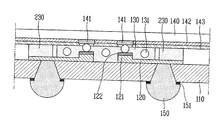
- 패드가 구비된 제1영역과, 상기 제1영역과 다른 위치에 제2영역이 구비된 반도체 소자;상기 패드에 대응되는 위치에 돌출부가 형성된 회로패턴을 구비하는 기판;상기 제1영역에 배치되어 상기 제1영역과 기판을 접착시키며, 상기 패드와 돌출부에 각각 접촉되는 도전체를 구비하는 제1접착층; 및상기 제2영역에 배치되며, 상기 제2영역과 기판을 접착시키는 비도전성 재질의 제2접착층을 포함하는 반도체 패키지.
- 제1항에 있어서,상기 반도체 소자는 와이어 본딩을 위하여 제조된 와이어 본딩용 웨이퍼로 형성되는 것을 특징으로 하는 반도체 패키지.
- 제1항에 있어서,상기 제1접착층은 이방성 전도 필름 또는 이방성 전도 페이스트으로 구현되며,상기 제2접착층은 비전도성 필름 또는 비전도성 페이스트로 구현되는 것을 특징으로 하는 반도체 패키지.
- 제1항에 있어서,상기 제2접착층은 상기 제2영역 중 일부 면적에 대응되는 크기를 갖는 것을 특징으로 하는 반도체 패키지.
- 패드가 구비된 제1영역과, 상기 제1영역과 다른 위치에 제2영역이 구비된 반도체 소자를 구비하는 반도체 패키지의 제조 방법에 있어서,기판의 일면에 회로패턴을 형성하는 단계;상기 회로패턴의 일면에 돌출부를 형성시키는 단계; 및도전체가 구비된 제1접착필름으로 상기 도전체가 상기 패드와 돌출부에 접촉되도록 상기 제1영역과 기판을 접착시키고, 비도전성 재질의 제2접착필름으로 상기 제2영역과 기판을 접착시키는 단계를 포함하는 반도체 패키지의 제조방법.
- 제5항에 있어서,상기 기판과 반도체 소자는 상기 제1 및 제2접착필름이 상기 기판과 반도체 소자의 사이에 위치한 상태에서 열압착에 의하여 서로 접착되는 것을 특징으로 하는 반도체 패키지의 제조방법.
Priority Applications (1)
| Application Number | Priority Date | Filing Date | Title |
|---|---|---|---|
| KR1020090095359A KR101119473B1 (ko) | 2009-10-07 | 2009-10-07 | 반도체 패키지 및 그 제조방법 |
Applications Claiming Priority (1)
| Application Number | Priority Date | Filing Date | Title |
|---|---|---|---|
| KR1020090095359A KR101119473B1 (ko) | 2009-10-07 | 2009-10-07 | 반도체 패키지 및 그 제조방법 |
Publications (2)
| Publication Number | Publication Date |
|---|---|
| KR20110037791A KR20110037791A (ko) | 2011-04-13 |
| KR101119473B1 true KR101119473B1 (ko) | 2012-03-16 |
Family
ID=44045215
Family Applications (1)
| Application Number | Title | Priority Date | Filing Date |
|---|---|---|---|
| KR1020090095359A Expired - Fee Related KR101119473B1 (ko) | 2009-10-07 | 2009-10-07 | 반도체 패키지 및 그 제조방법 |
Country Status (1)
| Country | Link |
|---|---|
| KR (1) | KR101119473B1 (ko) |
Citations (4)
| Publication number | Priority date | Publication date | Assignee | Title |
|---|---|---|---|---|
| KR19990069638A (ko) * | 1998-02-11 | 1999-09-06 | 윤종용 | 칩 스케일 패키지 및 그 제조방법 |
| JP2005286028A (ja) | 2004-03-29 | 2005-10-13 | Sharp Corp | 固体撮像素子パッケージ、半導体パッケージ、カメラモジュール、及び固体撮像素子パッケージの製造方法 |
| KR20070095865A (ko) * | 2004-10-18 | 2007-10-01 | 스태츠 칩팩, 엘티디. | 멀티 칩 리드 프레임 패키지 |
| KR20080084299A (ko) * | 2007-03-15 | 2008-09-19 | 주식회사 하이닉스반도체 | 웨이퍼 레벨 패키지 및 그의 제조방법 |
-
2009
- 2009-10-07 KR KR1020090095359A patent/KR101119473B1/ko not_active Expired - Fee Related
Patent Citations (4)
| Publication number | Priority date | Publication date | Assignee | Title |
|---|---|---|---|---|
| KR19990069638A (ko) * | 1998-02-11 | 1999-09-06 | 윤종용 | 칩 스케일 패키지 및 그 제조방법 |
| JP2005286028A (ja) | 2004-03-29 | 2005-10-13 | Sharp Corp | 固体撮像素子パッケージ、半導体パッケージ、カメラモジュール、及び固体撮像素子パッケージの製造方法 |
| KR20070095865A (ko) * | 2004-10-18 | 2007-10-01 | 스태츠 칩팩, 엘티디. | 멀티 칩 리드 프레임 패키지 |
| KR20080084299A (ko) * | 2007-03-15 | 2008-09-19 | 주식회사 하이닉스반도체 | 웨이퍼 레벨 패키지 및 그의 제조방법 |
Also Published As
| Publication number | Publication date |
|---|---|
| KR20110037791A (ko) | 2011-04-13 |
Similar Documents
| Publication | Publication Date | Title |
|---|---|---|
| US7061125B2 (en) | Semiconductor package with pattern leads and method for manufacturing the same | |
| KR100546374B1 (ko) | 센터 패드를 갖는 적층형 반도체 패키지 및 그 제조방법 | |
| JP3967133B2 (ja) | 半導体装置及び電子機器の製造方法 | |
| KR100266698B1 (ko) | 반도체 칩 패키지 및 그 제조방법 | |
| US6252298B1 (en) | Semiconductor chip package using flexible circuit board with central opening | |
| KR100324708B1 (ko) | 반도체장치 | |
| US20020125556A1 (en) | Stacking structure of semiconductor chips and semiconductor package using it | |
| JP2002026198A (ja) | 半導体装置及びその製造方法 | |
| KR100698526B1 (ko) | 방열층을 갖는 배선기판 및 그를 이용한 반도체 패키지 | |
| US20090200658A1 (en) | Circuit board structure embedded with semiconductor chips | |
| US7129572B2 (en) | Submember mounted on a chip of electrical device for electrical connection | |
| US7420814B2 (en) | Package stack and manufacturing method thereof | |
| JP2006339596A (ja) | インタポーザおよび半導体装置 | |
| US6992380B2 (en) | Package for semiconductor device having a device-supporting polymeric material covering a solder ball array area | |
| US20020179692A1 (en) | Pin attachment by a surface mounting method for fabricating organic pin grid array packages | |
| US7847414B2 (en) | Chip package structure | |
| KR20090098076A (ko) | 플립 칩 패키지 | |
| KR101119473B1 (ko) | 반도체 패키지 및 그 제조방법 | |
| KR19980025624A (ko) | 볼 그리드 어레이 반도체 패키지 | |
| KR101083004B1 (ko) | 반도체 패키지 및 그 제조방법 | |
| US20070075415A1 (en) | Semiconductor device and semiconductor device production method | |
| JP3841135B2 (ja) | 半導体装置、回路基板及び電子機器 | |
| US8039935B2 (en) | Wafer level chip scale packaging structure and method of fabricating the same | |
| KR20010058579A (ko) | 반도체패키지 및 이를 위한 웨이퍼의 상호 접착방법 | |
| KR20010073452A (ko) | 볼 그리드 어레이 패키지와 그에 이용되는 인쇄 회로 기판 |
Legal Events
| Date | Code | Title | Description |
|---|---|---|---|
| A201 | Request for examination | ||
| PA0109 | Patent application |
St.27 status event code: A-0-1-A10-A12-nap-PA0109 |
|
| PA0201 | Request for examination |
St.27 status event code: A-1-2-D10-D11-exm-PA0201 |
|
| PG1501 | Laying open of application |
St.27 status event code: A-1-1-Q10-Q12-nap-PG1501 |
|
| E902 | Notification of reason for refusal | ||
| PE0902 | Notice of grounds for rejection |
St.27 status event code: A-1-2-D10-D21-exm-PE0902 |
|
| P11-X000 | Amendment of application requested |
St.27 status event code: A-2-2-P10-P11-nap-X000 |
|
| P13-X000 | Application amended |
St.27 status event code: A-2-2-P10-P13-nap-X000 |
|
| E701 | Decision to grant or registration of patent right | ||
| PE0701 | Decision of registration |
St.27 status event code: A-1-2-D10-D22-exm-PE0701 |
|
| GRNT | Written decision to grant | ||
| PR0701 | Registration of establishment |
St.27 status event code: A-2-4-F10-F11-exm-PR0701 |
|
| PR1002 | Payment of registration fee |
St.27 status event code: A-2-2-U10-U11-oth-PR1002 Fee payment year number: 1 |
|
| PG1601 | Publication of registration |
St.27 status event code: A-4-4-Q10-Q13-nap-PG1601 |
|
| R18-X000 | Changes to party contact information recorded |
St.27 status event code: A-5-5-R10-R18-oth-X000 |
|
| R18-X000 | Changes to party contact information recorded |
St.27 status event code: A-5-5-R10-R18-oth-X000 |
|
| FPAY | Annual fee payment |
Payment date: 20150209 Year of fee payment: 4 |
|
| PR1001 | Payment of annual fee |
St.27 status event code: A-4-4-U10-U11-oth-PR1001 Fee payment year number: 4 |
|
| PC1903 | Unpaid annual fee |
St.27 status event code: A-4-4-U10-U13-oth-PC1903 Not in force date: 20160217 Payment event data comment text: Termination Category : DEFAULT_OF_REGISTRATION_FEE |
|
| FPAY | Annual fee payment |
Payment date: 20161111 Year of fee payment: 5 |
|
| K11-X000 | Ip right revival requested |
St.27 status event code: A-6-4-K10-K11-oth-X000 |
|
| PC1903 | Unpaid annual fee |
St.27 status event code: N-4-6-H10-H13-oth-PC1903 Ip right cessation event data comment text: Termination Category : DEFAULT_OF_REGISTRATION_FEE Not in force date: 20160217 |
|
| PR0401 | Registration of restoration |
St.27 status event code: A-6-4-K10-K13-oth-PR0401 |
|
| PR1001 | Payment of annual fee |
St.27 status event code: A-4-4-U10-U11-oth-PR1001 Fee payment year number: 5 |
|
| R401 | Registration of restoration | ||
| LAPS | Lapse due to unpaid annual fee | ||
| PC1903 | Unpaid annual fee |
St.27 status event code: A-4-4-U10-U13-oth-PC1903 Not in force date: 20170217 Payment event data comment text: Termination Category : DEFAULT_OF_REGISTRATION_FEE |
|
| PC1903 | Unpaid annual fee |
St.27 status event code: N-4-6-H10-H13-oth-PC1903 Ip right cessation event data comment text: Termination Category : DEFAULT_OF_REGISTRATION_FEE Not in force date: 20170217 |
|
| P22-X000 | Classification modified |
St.27 status event code: A-4-4-P10-P22-nap-X000 |