KR101119473B1 - Semiconductor package and method for manufacturing the same - Google Patents
Semiconductor package and method for manufacturing the same Download PDFInfo
- Publication number
- KR101119473B1 KR101119473B1 KR1020090095359A KR20090095359A KR101119473B1 KR 101119473 B1 KR101119473 B1 KR 101119473B1 KR 1020090095359 A KR1020090095359 A KR 1020090095359A KR 20090095359 A KR20090095359 A KR 20090095359A KR 101119473 B1 KR101119473 B1 KR 101119473B1
- Authority
- KR
- South Korea
- Prior art keywords
- region
- substrate
- semiconductor device
- semiconductor package
- pad
- Prior art date
- Legal status (The legal status is an assumption and is not a legal conclusion. Google has not performed a legal analysis and makes no representation as to the accuracy of the status listed.)
- Expired - Fee Related
Links
Images


Classifications
-
- H10W72/00—
-
- H10W72/20—
Landscapes
- Wire Bonding (AREA)
Abstract
본 발명은 패드가 구비된 제1영역과 상기 제1영역과 다른 위치에 제2영역이 구비된 반도체 소자와; 상기 패드에 대응되는 위치에 돌출부가 형성된 회로패턴을 구비하는 기판과, 상기 제1영역에 배치되어 상기 제1영역과 기판을 접착시키며 상기 패드와 돌출부에 각각 접촉되는 도전체를 구비하는 제1접착층, 및 상기 제2영역에 배치되며 상기 제2영역과 기판을 접착시키는 비도전성 재질의 제2접착층을 포함하는 반도체 패키지 및 그 제조방법을 개시한다.The present invention provides a semiconductor device comprising a first region including a pad and a second region disposed at a position different from the first region; A first adhesive layer having a substrate having a circuit pattern having a protrusion formed at a position corresponding to the pad, and a conductor disposed in the first region to bond the first region and the substrate to contact the pad and the protrusion, respectively; And a second adhesive layer of a non-conductive material disposed on the second region and adhering the second region to the substrate, and a method of manufacturing the same.
Description
본 발명은 반도체 소자가 실장된 반도체 패키지 및 그 제조방법에 관한 것이다.The present invention relates to a semiconductor package having a semiconductor device mounted thereon and a method of manufacturing the same.
반도체 패키지(Semiconductor Package)는 반도체 소자를 외부의 물리적, 전기적 충격으로부터 보호하고 반도체 소자를 전자기기와 전기적으로 연결시킴으로써 반도체가 그 기능을 구현하도록 하기 위한 구조를 말하며, 메모리, 주문형 반도체 등 다양한 형태로 구현되고 있다.A semiconductor package is a structure for protecting a semiconductor device from external physical and electrical shocks and electrically connecting the semiconductor device to an electronic device to implement the function. Is being implemented.
이러한 반도체 패키지는 일반적으로 반도체 소자가 실장된 기판의 형태를 가지며, 이러한 반도체 패키지는 전자 기기의 메인 보드에 실장된다.Such a semiconductor package generally has a form of a substrate on which a semiconductor device is mounted, and the semiconductor package is mounted on a main board of an electronic device.
반도체 소자를 기판에 전기적으로 연결시키는 방법으로 와이어 본딩(wire bonding)과 플립칩 본딩(flip-chip bonding)을 들 수 있다.Wire bonding and flip-chip bonding may be used as a method of electrically connecting a semiconductor device to a substrate.
와이어 본딩은 반도체 소자를 기판에 연결할 때 와이어를 사용하는 방법으로, 대부분의 일반적인 반도체 패키지에 사용되고 있다.Wire bonding is a method of using a wire when connecting a semiconductor device to a substrate, and is used in most general semiconductor packages.
플립칩 본딩은 와이어를 사용하지 않고 반도체 소자에 볼 형태의 범프를 형 성시킨 다음, 이를 기판에 직접 부착하여 반도체 소자와 기판을 전기적으로 연결하는 방법이다. 플립칩 본딩을 이용한 반도체 패키지는 전기적 연결통로의 길이가 와이어 본딩과 대비하여 훨씬 짧아져 향상된 전기적 성능을 얻을 수 있고, 배선 밀도를 증가시켜 패키지의 크기를 작게 할 수 있는 장점이 있다.Flip chip bonding is a method of electrically connecting a semiconductor device and a substrate by forming a ball-shaped bump on a semiconductor device without using a wire and then directly attaching it to the substrate. The semiconductor package using the flip chip bonding has an advantage that the length of the electrical connection path is much shorter than that of the wire bonding to obtain improved electrical performance, and to reduce the size of the package by increasing the wiring density.
그러나 플립칩 본딩을 이용할 경우, 웨이퍼(wafer) 상에 RDL(Re-Distribution Layer)를 형성하여야 함과 아울러 반도체 소자 상에 범프를 형성시키는 공정이 추가적으로 수행되어야 하므로 비용이 증가한다. 아울러, 기판의 배선 밀도를 증가시키기 위한 공정의 증가 또한 비용 상승의 원인이 된다.However, in the case of using flip chip bonding, a cost must be increased because a process of forming bumps on a semiconductor device must be performed as well as a re-distribution layer (RDL) on a wafer. In addition, an increase in the process for increasing the wiring density of the substrate also causes a cost increase.
이와 같이, 플립칩 본딩을 이용한 반도체 패키지는 그 성능의 우수성에도 불구하고 고비용이 소요되는 문제로 인하여 널리 이용되지 못하고 있는 실정이다.As such, a semiconductor package using flip chip bonding is not widely used due to a problem of high cost despite its superior performance.
본 발명은 상기와 같은 문제점을 해결하기 위한 것으로서, 간단한 구조로서 저비용으로 제조 가능하면서도 우수한 전기적 성능을 갖는 반도체 패키지의 구조 및 그 제조방법을 제공하기 위한 것이다. The present invention is to solve the above problems, to provide a structure and a method of manufacturing a semiconductor package that can be manufactured at a low cost as a simple structure and having excellent electrical performance.
상기한 과제를 실현하기 위해 본 발명은 패드가 구비된 제1영역과 상기 제1영역과 다른 위치에 제2영역이 구비된 반도체 소자와, 상기 패드에 대응되는 위치에 돌출부가 형성된 회로패턴을 구비하는 기판과, 상기 제1영역에 배치되어 상기 제1영역과 기판을 접착시키며 상기 패드와 돌출부에 각각 접촉되는 도전체를 구비하는 제1접착층, 및 상기 제2영역에 배치되며 상기 제2영역과 기판을 접착시키는 비도전성 재질의 제2접착층을 포함하는 반도체 패키지를 개시한다.In order to achieve the above object, the present invention includes a semiconductor device having a first region provided with a pad, a second region provided at a position different from the first region, and a circuit pattern having a protrusion formed at a position corresponding to the pad. A first adhesive layer having a substrate disposed in the first region, the first adhesive layer having a conductor adhering the substrate to the pad and the protruding portion, and a second adhesive layer disposed in the second region. A semiconductor package comprising a second adhesive layer of a non-conductive material for adhering a substrate is disclosed.
상기 반도체 소자는 와이어 본딩을 위하여 제조된 와이어 본딩용 웨이퍼로 형성될 수 있다.The semiconductor device may be formed of a wire bonding wafer manufactured for wire bonding.
상기 제1접착층은 이방성 전도 필름(ACF; Anisotropic Conductive Film) 또는 이방성 전도 페이스트(Anisotropic Conductive Paste)으로 구현되며, 상기 제2접착층은 비전도성 필름(NCF; Non-Conductive Film) 또는 비전도성 페이스트(Non-Conductive Paste)으로 구현될 수 있다.The first adhesive layer is formed of an anisotropic conductive film (ACF) or an anisotropic conductive paste (Anisotropic Conductive Paste), the second adhesive layer is a non-conductive film (NCF) or non-conductive paste (Non) -Conductive Paste).
상기 제2접착층은 상기 제2영역 중 일부 면적에 대응되는 크기를 가질 수 있다.The second adhesive layer may have a size corresponding to a partial area of the second region.
한편, 본 발명은 패드가 구비된 제1영역과, 상기 제1영역과 다른 위치에 제2영역이 구비된 반도체 소자를 구비하는 반도체 패키지의 제조 방법에 있어서, 기판의 일면에 회로패턴을 형성하는 단계와, 상기 회로패턴의 일면에 돌출부를 형성시키는 단계, 및 도전체가 구비된 제1접착필름으로 상기 도전체가 상기 패드와 돌출부에 접촉되도록 상기 제1영역과 기판을 접착시키고, 비도전성 재질의 제2접착필름으로 상기 제2영역과 기판을 접착시키는 단계를 포함하는 반도체 패키지의 제조방법을 개시한다.Meanwhile, the present invention provides a method of manufacturing a semiconductor package including a first region having a pad and a semiconductor device having a second region at a position different from the first region, the circuit pattern being formed on one surface of a substrate. Forming a protrusion on one surface of the circuit pattern, and adhering the substrate to the first region and the substrate such that the conductor contacts the pad and the protrusion with a first adhesive film provided with a conductor. Disclosed is a method of manufacturing a semiconductor package comprising adhering the second region and a substrate to a second adhesive film.
본 발명에 의하면, 와이어 본딩용 웨이퍼를 반도체 소자로 사용함으로써 제조 비용을 절감하였으며, 반도체 소자와 기판을 부착하기 위한 구조로서 도전체를 갖는 접착 물질을 사용하여 전기적 연결 통로의 길이를 감소시킴으로써 우수한 전기적 성능을 얻을 수 있다.According to the present invention, the manufacturing cost is reduced by using the wire bonding wafer as a semiconductor element, and the electrical connection path is reduced by using an adhesive material having a conductor as a structure for attaching the semiconductor element and the substrate. You can get performance.
또한, 본 발명은 기판의 회로패턴에 돌출부를 형성시킴으로써 플립칩 본딩에 대비하여 간단한 제조 공정을 통하여 기판과 반도체 소자 사이의 전기적 연결의 안정성을 향상시킬 수 있다. In addition, the present invention can improve the stability of the electrical connection between the substrate and the semiconductor device through a simple manufacturing process in preparation for flip chip bonding by forming a protrusion on the circuit pattern of the substrate.
또한, 본 발명은 플립칩 본딩과 같이 기판의 재배선 공정을 추가하지 않고 본딩용 범프를 추가하지 않아도 되기 때문에 그에 따른 비용 절감 효과를 가질 수 있다.In addition, since the present invention does not need to add a bump for bonding and does not add a rearrangement process of a substrate, such as flip chip bonding, the present invention may have a cost reduction effect.
또한, 반도체의 패드가 구비된 영역을 제외한 영역은 비교적 저렴한 비도전성 재질의 접착필름(또는 페이스트)으로 기판에 부착하여 제조 비용을 감소시킬 수 있다. 아울러, 반도체 소자와 기판이 접착 면적을 최소화함으로써, 제조 공정 상에 있어서 반도체 패키지의 열변형에 대한 대응력을 향상시킬 수 있다.In addition, the region except for the region in which the pad is provided in the semiconductor may be attached to the substrate using a relatively inexpensive non-conductive adhesive film (or paste), thereby reducing manufacturing costs. In addition, by minimizing the adhesion area between the semiconductor device and the substrate, it is possible to improve the ability to respond to thermal deformation of the semiconductor package in the manufacturing process.
이하, 본 발명에 관련된 반도체 패키지 및 그 제조방법에 대하여 도면을 참조하여 보다 상세하게 설명한다.EMBODIMENT OF THE INVENTION Hereinafter, the semiconductor package which concerns on this invention, and its manufacturing method are demonstrated in detail with reference to drawings.
도 1 내지 도 7은 본 발명의 일실시예와 관련된 반도체 패키지의 제조공정을 나타내는 도면들이다.1 to 7 are views illustrating a manufacturing process of a semiconductor package according to an embodiment of the present invention.
도 1을 참조하면, 기판(110)에 회로패턴(120)을 형성시킨다. 기판(110)은 반도체 소자(140, 도 5 참조)를 지지함과 아울러 전기 신호를 전달하기 위한 매개체로서의 기능을 하기 위한 것이다. 기판(110)은 절연성 재질로 형성되며, 에폭시 수지, 페놀 수지, 폴리이미드 등의 재질로 형성될 수 있다.Referring to FIG. 1, a
도 8은 본 발명과 관련된 반도체 패키지에 적용되는 반도체 소자의 일 예를 나타내는 사시도이다.8 is a perspective view illustrating an example of a semiconductor device applied to a semiconductor package according to the present invention.
본 실시예에 의하면, 반도체 소자(140, 또는 반도체 칩, 웨이퍼 등)로서 와이어 본딩을 위하여 제조된 와이어 본딩용 웨이퍼가 사용된다. 플립칩 본딩용 웨이퍼는 웨이퍼 상에 RDL(Re-Distribution Layer)를 형성하여야 함과 아울러 반도체 소자 상에 범프를 형성시키는 공정이 추가적으로 수행되어야 하므로 제조 비용이 증가하게 된다.According to the present embodiment, a wire bonding wafer manufactured for wire bonding is used as the
본 발명에서는 제조 비용의 감소를 위하여 도 8과 같은 저가의 와이어 본딩용 웨이퍼를 사용하였다. 물론, 플립칩 본딩용으로 만들어져 있는 웨이퍼의 사용도 가능하다 할 것이다.In the present invention, inexpensive wire bonding wafers as shown in FIG. 8 are used to reduce manufacturing costs. Of course, it is also possible to use wafers made for flip chip bonding.
반도체 소자(140)의 일면에는 제1영역(Ⅰ)과, 제1영역(Ⅰ)과 다른 위치에 형성된 제2영역(Ⅱ)이 구비된다. 제1영역(Ⅰ)은 반도체 소자(140)의 중앙 영역에 형성되며, 제2영역(Ⅱ)은 제1영역(Ⅰ)의 주변을 한정하도록 형성될 수 있다.One surface of the
제1영역(Ⅰ)에는 기판(110)과의 전기적 연결을 위한 복수의 패드(141)들이 구비되어 있다. 본 실시예에 의하면, 패드(141)들은 2열의 형태로서 사이에 일정 간격을 갖도록 배열되어 있다.In the first region I, a plurality of
다시 도 1을 참조하면, 기판(110) 상에 형성된 도전성 물질을 일정 패턴을 갖도록 에칭하여 회로패턴(120)을 형성시킨다. Referring to FIG. 1 again, the conductive material formed on the
회로패턴(120)을 형성시키기 전 또는 후, 기판(110) 상에 비아홀(111)을 형성시킨다. 비아홀(111)은 기판(110)의 양면을 전기적으로 도통시키기 위한 것으로서, 기판(110)을 드릴, 레이저 드릴로 가공하거나 플라즈마 또는 약품에 의한 에칭함으로써 형성될 수 있다.Before or after the
다음으로, 도 2와 같이 회로패턴(120)의 일면에 돌출부(121)를 형성시킨다. 돌출부(121)는 반도체(140)의 실장치 패드(141)의 위치에 대응되는 위치에 형성된다.Next, as shown in FIG. 2, the
본 실시예에 의하면,회로패턴(120)의 일부 영역을 에칭하여 일정 두께의 단차(t)를 형성시킴으로써 돌출부(121)를 형성시켰다. 다만, 돌출부(121)는 이러한 방법 이외에도 애디티브 방식으로 도금을 실시함에 의하여 형성될 수 있다. According to the present embodiment, the
다음으로, 도 3과 같이 돌출부(121)의 표면에 산화 방지를 위한 산화 방지 층(122)을 형성시킬 수 있다. 산화 방지층(122)은 금(Au), 은(Ag), 주석(Sn)과 같은 물질을 돌출부(121)의 표면에 도금 처리함으로써 형성될 수 있다.Next, as shown in FIG. 3, an
그리고, 회로패턴(120)의 표면을 보호하기 위하여 회로패턴(120)의 표면을 산화 처리할 수 있다. 산화 처리에 의하여 회로패턴(120)의 표면에는 산화 피막(123)이 형성된다. 이러한 산화 피막(123)은 회로패턴(120)의 보호 이외에도 회로패턴(120)과 몰드(160, 도 9 참조) 또는 접착 필름(130, 또는 페이스트)과의 접착력을 향상시키는 기능을 한다.In addition, the surface of the
다음으로, 도 4와 같이 회로패턴(120)의 일면에 제1접착필름(130)과 제2접착필름(230)들을 위치시킨다. 제1 및 제2접착필름(130,140)은 페이스트(paste)로 대체 가능하며, 이하에서는 접착필름을 사용하는 것을 기초로 설명하기로 한다.Next, as shown in FIG. 4, the first
제1접착필름(130)은 반도체 소자(140)의 실장시 반도체 소자(140)의 제1영역(Ⅰ)에 대응되는 위치에 놓이게 된다. 제1접착필름(130)은 반도체 소자(140)의 제1영역(Ⅰ)과 기판(110)을 접착시키고, 반도체 소자(140)와 기판(110)을 전기적으로 연결하기 위한 것이다. The first
제1접착필름(130)은 비도전성 재질의 접착 물질로 형성되며, 내부에 도전체(131)들이 복수로 배열된다. 도전체(131)들은 입자 형태로 형성될 수 있으며, 그 밖에 로드 형태를 가질 수 있다. 이하에서는 도전체(131)를 도전 입자(131)라 지칭하기로 한다.The first
도전입자(131)들은 접착 필름(130)의 내부에 일정한 간격을 갖도록 복수로 배열된다. 접착 필름(130)의 일 형태로서 이방전도성 물질이 사용될 수 있으며, 본 실시예에서는 이방전도성 필름(ACF: An-isotropic Conductive Film)이 사용되었다.The
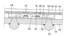
제2접착필름(230)들은 반도체 소자(140)의 실장시 반도체(140)의 제2영역(Ⅱ)에 대응되는 위치에 놓이게 된다. 즉, 제2접착필름(230)들은 제1접착필름(130)의 외부에 각각 놓일 수 있다. 제2접착필름(230)은 반도체 소자(140)의 제2영역(Ⅱ)과 기판(110)을 접착시키기 위한 것으로서, 비도전성 재질의 접착 물질로 형성된다.The second
특히, 본 실시예와 같이 반도체 소자(140)의 중앙 영역에 패드(141)들이 배열되어 있는 경우, 제2접착필름(230)들은 위와 같은 접착 기능을 함과 아울러 반도체 소자(140)의 접착 과정에서 반도체 소자(140)가 좌우로 기울어지는 것을 방지한다. 즉, 반도체 소자(140)의 접착시 반도체 소자(140)의 수평 자세를 유지시키는 기능도 함께 수행한다 할 것이다.In particular, when the
제2접착필름(230)들은 반도체 소자(140)의 제2영역(Ⅱ) 전체를 기판에 부착시키도록 구성될 수도 있으나, 본 실시예에 따르면 제2접착필름(230)들은 제2영역(Ⅱ) 중 일부 면적만을 기판(110)에 부착시키도록 구성된다. 예를 들어, 제2접착필름(230)들은 도 8에 도시된 접착 면적(Ⅲ)에 해당하는 부분만 접착시키기 위한 크기와 위치를 갖는다. The second
제2영역(Ⅱ)의 일부 면적 만이 기판(110)에 부착되는 경우, 제2영역(Ⅱ)의 나머지 부분은 기판(110)에 접착되지 않게 된다. 이는 반도체 소자(140)와 기판(110)의 접착 면적을 최소화함으로써, 반도체 소자(140)와 기판(110)의 열팽창 계수(CTE)의 차이로 인해 박리 현상으로 인한 불량이 발생하는 것을 방지하기 위함 이다. When only a part of the area of the second region II is attached to the
다음으로, 도 5와 같이 제1 및 제2접착필름(130,230)에 부착되어 있는 보호 필름들(132,232)을 벗겨 내고, 제1 및 제2접착필름(130,230)의 일면에 반도체 소자(140)를 위치시킨다.Next, as shown in FIG. 5, the
반도체 소자(140)의 패드(141)에는 회로패턴(142)이 연결되며, 회로패턴(142)의 표면에는 회로패턴(142)을 보호하기 위한 보호층(143)이 형성될 수 있다. 여기서 보호층(143)은 패드(141)의 주변을 한정하도록 회로패턴(142)에 형성된다.The
반도체 소자(140)를 접착 필름(130) 상에 위치시킬 때, 반도체 소자(140)의 패드(141)와 기판(110)의 돌출부(121)가 서로 대응하는 위치에서 마주볼 수 있도록 반도체 소자(140)를 위치시킨다.When the
다음으로, 도 6과 같이 반도체 소자(140)와 기판(110)을 열압착하여 반도체 소자(140)와 기판(110)을 접착시킨다. 반도체 소자(140)와 기판(110) 사이에 위치한 제1 및 제2접착필름(130,230)이 열에 의하여 용융된 후 경화되게 되며, 이에 따라 반도체 소자(140)와 기판(110)이 접착되게 된다. 앞서 설명된 바와 같이, 반도체 소자(140)의 제1영역(Ⅰ)은 제1접착필름(130)에 의해 기판(110)에 접착되며, 반도체 소자(140)의 제2영역(Ⅱ)은 제2접착필름(230)에 의해 기판(110)에 접착되게 된다.Next, as shown in FIG. 6, the
이 과정에서, 복수의 도전입자(131)들 중 적어도 하나의 도전입자(131)가 패드(141)와 돌출부(121)에 각각 접촉하게 된다. 도전입자(131)는 패드(141)와 돌출 부(121)에 각각 접촉됨으로써, 반도체 소자(140)의 회로패턴(142)과 기판(110)의 회로패턴(120)을 전기적으로 연결시킨다.In this process, at least one
본 발명에 의한 반도체 패키지는 기판(110)의 회로패턴(120)에 돌출부(121)가 형성된 구조를 가짐으로써, 기판(110)과 반도체 소자(140)의 전기적 접속이 보다 안정적으로 이루어질 수 있도록 한다. 예를 들어, 반도체 소자(140)의 보호층(143)은 패드(141)에 대하여 일정 깊이의 단차(d)를 형성하며, 이러한 단차(d)는 도전입자(131)가 패드(141)에 접촉되지 못하게 하는 하나의 요인이 될 수 있다. 돌출부(121)는 도전입자(131)가 패드(141)에 안정적으로 접촉될 수 있도록 도전입자(131)의 접촉을 가이드하는 기능을 한다.The semiconductor package according to the present invention has a structure in which the
참고로, 기판(110)은 와이어 본딩용 웨이퍼, 즉 반도체 소자(140)에 대응되는 크기를 갖거나, 복수의 와이어 본딩용 웨이퍼가 배열 가능한 크기로 형성될 수 있다. 기판(110)이 복수의 와이어 본딩용 웨이퍼가 배열 가능한 크기를 갖는 경우, 기판(110)과 웨이퍼의 접착 후 절단하는 공정이 추가될 것이다.For reference, the
다음으로, 도 7과 같이 기판(110)의 타면에 솔더볼(150)을 충전시킨다. 솔더볼(150)은 반도체 패키지를 다른 기판에 실장하도록 하기 위한 것으로서, 솔더볼(150)은 비아홀(111)이 내부로 충전되어 기판(110)의 회로패턴(120)에 연결된다. 이와 같이, 솔더볼(150)의 충전 단계는 도 1과 같은 회로패턴(120)의 형성 단계에서 행하여지는 것도 가능하다 할 것이다.Next, as shown in FIG. 7, the
여기서. 기판(110)에 솔더볼(150)의 접착을 위한 접착 패드(151)가 추가적으로 구비될 수 있다. 솔더볼(150)의 충전시 솔더볼(150)이 접착 패드(151)에 부착됨 에 따라 솔더볼(150)은 안정적으로 자리매김될 수 있다.here. An
이와 같이 기판(110)의 일면에 산화 처리된 회로패턴(120)을 형성시키고, 이를 기판(110) 타면의 솔더볼(150)로 연결하는 구조에 의하면, 회로패턴(120)을 땜납으로부터 보호하기 위한 솔더 레지스트의 적층과 같은 추가적인 공정이 필요치 않게 되며, 이에 따라 보다 단순한 제조공정과 간단한 구조의 반도체 패키지가 제공될 수 있다.As described above, according to the structure in which the
도 9는 본 발명과 관련된 반도체 패키지에 적용되는 반도체 소자의 다른 예를 나타내는 사시도이다.9 is a perspective view showing another example of a semiconductor device applied to a semiconductor package according to the present invention.
본 실시예에 의하면, 제2영역(Ⅱ)이 반도체 소자(140)의 중앙 영역에 형성되고, 제1영역(Ⅰ)이 제2영역(Ⅱ)의 주변을 한정하도록 형성된다. 제1영역(Ⅰ)에 기판과의 전기적 연결을 위한 복수의 패드(141)들이 배치된다. 패드들(141)은 제2영역(Ⅱ)의 주변을 따라 배열되며, 이러한 배열은 소위 '주변 배열'이라 불릴 수 있다.According to the present embodiment, the second region II is formed in the central region of the
이러한 경우, 앞서 설명된 제2접착필름(230)이 반도체 소자(140) 중앙 영역의 제2영역(Ⅱ)에 위치하며, 제1접착필름(130)이 그 외곽의 제1영역(Ⅰ)에 위치하게 될 것이다.In this case, the second
도 10은 이상에서 설명된 바와 같은 제조공정에 의하여 제조된 반도체 패키지의 일예를 나타내는 도면이다.FIG. 10 is a diagram illustrating an example of a semiconductor package manufactured by a manufacturing process as described above.
반도체 패키지는 제1영역(Ⅰ)과 제2영역(Ⅱ)이 구비된 반도체 소자(140)와, 돌출부(121)가 형성된 회로패턴(120)을 구비하는 기판(110)과, 반도체 소자(140)의 제1영역(Ⅰ)과 기판(110)을 접착시키는 제1접착층(130')과, 반도체 소자(140)의 제2영역(Ⅱ)과 기판(110)을 접착시키는 제2접착층(230')들을 포함한다. 여기서, 제1접착층(130')과 제2접착층(230')은 앞서 설명된 제1접착필름(130)과 제2접착필름(230)에 의해 형성된다.The semiconductor package includes a
인쇄회로기판(110)의 일면에는 반도체 소자(140)를 외부로부터 보호하기 위한 몰드(160)가 구비될 수 있다. 몰드(160)는 합성 수지 재질로 형성될 수 있으며, 반도체 소자(140)를 덮도록 형성된다.One surface of the printed
이와 같은, 반도체 패키지(100)는 솔더볼(150)에 의하여 다른 기판, 예를 들면 전자기기의 메인 기판(200)에 실장될 수 있다. As such, the
본 발명에 따르면, 와이어 본딩용 웨이퍼를 반도체 소자(140)로 사용함으로써 제조 비용을 절감하였다. 그리고, 반도체 소자(140)와 기판(110)의 부착하기 위한 구조로서 도전입자(131)를 갖는 제1접착필름(130)을 사용하여, 전기적 연결 통로의 길이를 감소시킴으로써 우수한 전기적 성능을 얻을 수 있다.According to the present invention, the manufacturing cost is reduced by using the wire bonding wafer as the
또한, 기판(110)의 회로패턴(120)에 돌출부(121)를 형성시킴으로써, 간단한 제조 공정을 통하여 기판(110)과 반도체 소자(140) 사이의 전기적 연결의 안정성을 향상시킬 수 있다. 그리고, 플립칩 본딩과 같이 기판의 배선 밀도를 증가시키지 않아도 되기 때문에 그에 따른 비용 절감 효과 또한 가질 수 있다.In addition, by forming the
아울러, 패드(141)가 구비된 영역을 제외한 영역, 즉 제2영역(Ⅱ)은 비교적 저렴한 비도전성 재질의 제2접착필름으로 부착하여 제조 비용을 감소시켰다. 또한, 제2영역(Ⅱ)의 일부만을 기판(110)과 접착시켜 반도체 소자(140)와 기판(110)의 접 착 면적을 감소시킴으로써, 반도체 소자(140)와 기판(110)의 열팽창 계수(CTE)의 차이로 인해 반도체 소자(140)와 기판(110) 사이에 박리 현상이 발생하는 것을 방지할 수 있다.In addition, the region except for the region where the
이상에서 설명한 반도체 패키지 및 그 제조방법은 위에서 설명된 실시예들의 구성과 방법에 한정되는 것이 아니라, 상기 실시예들은 다양한 변형이 이루어질 수 있도록 각 실시예들의 전부 또는 일부가 선택적으로 조합되어 구성될 수도 있다.The above-described semiconductor package and its manufacturing method are not limited to the configuration and method of the above-described embodiments, but the above embodiments may be configured by selectively combining all or some of the embodiments so that various modifications can be made. have.
도 1 내지 도 7은 본 발명의 일실시예와 관련된 반도체 패키지의 제조공정을 나타내는 도면.1 to 7 are views illustrating a manufacturing process of a semiconductor package according to an embodiment of the present invention.
도 8은 본 발명과 관련된 반도체 패키지에 적용되는 반도체 소자의 일 예를 나타내는 사시도.8 is a perspective view showing an example of a semiconductor device applied to a semiconductor package according to the present invention.
도 9는 본 발명과 관련된 반도체 패키지에 적용되는 반도체 소자의 다른 예를 나타내는 사시도.9 is a perspective view showing another example of a semiconductor device applied to a semiconductor package according to the present invention.
도 10은 본 발명의 일실시예와 관련된 반도체 패키지를 나타내는 도면.10 illustrates a semiconductor package according to an embodiment of the present invention.
Claims (6)
Priority Applications (1)
| Application Number | Priority Date | Filing Date | Title |
|---|---|---|---|
| KR1020090095359A KR101119473B1 (en) | 2009-10-07 | 2009-10-07 | Semiconductor package and method for manufacturing the same |
Applications Claiming Priority (1)
| Application Number | Priority Date | Filing Date | Title |
|---|---|---|---|
| KR1020090095359A KR101119473B1 (en) | 2009-10-07 | 2009-10-07 | Semiconductor package and method for manufacturing the same |
Publications (2)
| Publication Number | Publication Date |
|---|---|
| KR20110037791A KR20110037791A (en) | 2011-04-13 |
| KR101119473B1 true KR101119473B1 (en) | 2012-03-16 |
Family
ID=44045215
Family Applications (1)
| Application Number | Title | Priority Date | Filing Date |
|---|---|---|---|
| KR1020090095359A Expired - Fee Related KR101119473B1 (en) | 2009-10-07 | 2009-10-07 | Semiconductor package and method for manufacturing the same |
Country Status (1)
| Country | Link |
|---|---|
| KR (1) | KR101119473B1 (en) |
Citations (4)
| Publication number | Priority date | Publication date | Assignee | Title |
|---|---|---|---|---|
| KR19990069638A (en) * | 1998-02-11 | 1999-09-06 | 윤종용 | Chip scale package and its manufacturing method |
| JP2005286028A (en) | 2004-03-29 | 2005-10-13 | Sharp Corp | Solid-state image sensor package, semiconductor package, camera module, and method for manufacturing solid-state image sensor package |
| KR20070095865A (en) * | 2004-10-18 | 2007-10-01 | 스태츠 칩팩, 엘티디. | Multi Chip Lead Frame Package |
| KR20080084299A (en) * | 2007-03-15 | 2008-09-19 | 주식회사 하이닉스반도체 | Wafer level package and manufacturing method thereof |
-
2009
- 2009-10-07 KR KR1020090095359A patent/KR101119473B1/en not_active Expired - Fee Related
Patent Citations (4)
| Publication number | Priority date | Publication date | Assignee | Title |
|---|---|---|---|---|
| KR19990069638A (en) * | 1998-02-11 | 1999-09-06 | 윤종용 | Chip scale package and its manufacturing method |
| JP2005286028A (en) | 2004-03-29 | 2005-10-13 | Sharp Corp | Solid-state image sensor package, semiconductor package, camera module, and method for manufacturing solid-state image sensor package |
| KR20070095865A (en) * | 2004-10-18 | 2007-10-01 | 스태츠 칩팩, 엘티디. | Multi Chip Lead Frame Package |
| KR20080084299A (en) * | 2007-03-15 | 2008-09-19 | 주식회사 하이닉스반도체 | Wafer level package and manufacturing method thereof |
Also Published As
| Publication number | Publication date |
|---|---|
| KR20110037791A (en) | 2011-04-13 |
Similar Documents
| Publication | Publication Date | Title |
|---|---|---|
| US7061125B2 (en) | Semiconductor package with pattern leads and method for manufacturing the same | |
| KR100546374B1 (en) | Multilayer semiconductor package having a center pad and its manufacturing method | |
| JP3967133B2 (en) | Manufacturing method of semiconductor device and electronic device | |
| KR100266698B1 (en) | Semiconductor chip package and fabrication method thereof | |
| US6252298B1 (en) | Semiconductor chip package using flexible circuit board with central opening | |
| KR100324708B1 (en) | A semiconductor device | |
| US20020125556A1 (en) | Stacking structure of semiconductor chips and semiconductor package using it | |
| JP2002026198A (en) | Semiconductor device and manufacturing method thereof | |
| KR100698526B1 (en) | A wiring board having a heat dissipation layer and a semiconductor package using the same | |
| US20090200658A1 (en) | Circuit board structure embedded with semiconductor chips | |
| US7129572B2 (en) | Submember mounted on a chip of electrical device for electrical connection | |
| US7420814B2 (en) | Package stack and manufacturing method thereof | |
| JP2006339596A (en) | Interposer and semiconductor device | |
| US6992380B2 (en) | Package for semiconductor device having a device-supporting polymeric material covering a solder ball array area | |
| US20020179692A1 (en) | Pin attachment by a surface mounting method for fabricating organic pin grid array packages | |
| US7847414B2 (en) | Chip package structure | |
| KR20090098076A (en) | Flip chip package | |
| KR101119473B1 (en) | Semiconductor package and method for manufacturing the same | |
| KR19980025624A (en) | Ball Grid Array Semiconductor Package | |
| KR101083004B1 (en) | Semiconductor package and method for manufacturing the same | |
| US20070075415A1 (en) | Semiconductor device and semiconductor device production method | |
| JP3841135B2 (en) | Semiconductor device, circuit board and electronic equipment | |
| US8039935B2 (en) | Wafer level chip scale packaging structure and method of fabricating the same | |
| KR20010058579A (en) | semiconductor package and attaching method of wafer for same | |
| KR20010073452A (en) | Ball grid array package and printed circuit board used in the same |
Legal Events
| Date | Code | Title | Description |
|---|---|---|---|
| A201 | Request for examination | ||
| PA0109 | Patent application |
St.27 status event code: A-0-1-A10-A12-nap-PA0109 |
|
| PA0201 | Request for examination |
St.27 status event code: A-1-2-D10-D11-exm-PA0201 |
|
| PG1501 | Laying open of application |
St.27 status event code: A-1-1-Q10-Q12-nap-PG1501 |
|
| E902 | Notification of reason for refusal | ||
| PE0902 | Notice of grounds for rejection |
St.27 status event code: A-1-2-D10-D21-exm-PE0902 |
|
| P11-X000 | Amendment of application requested |
St.27 status event code: A-2-2-P10-P11-nap-X000 |
|
| P13-X000 | Application amended |
St.27 status event code: A-2-2-P10-P13-nap-X000 |
|
| E701 | Decision to grant or registration of patent right | ||
| PE0701 | Decision of registration |
St.27 status event code: A-1-2-D10-D22-exm-PE0701 |
|
| GRNT | Written decision to grant | ||
| PR0701 | Registration of establishment |
St.27 status event code: A-2-4-F10-F11-exm-PR0701 |
|
| PR1002 | Payment of registration fee |
St.27 status event code: A-2-2-U10-U11-oth-PR1002 Fee payment year number: 1 |
|
| PG1601 | Publication of registration |
St.27 status event code: A-4-4-Q10-Q13-nap-PG1601 |
|
| R18-X000 | Changes to party contact information recorded |
St.27 status event code: A-5-5-R10-R18-oth-X000 |
|
| R18-X000 | Changes to party contact information recorded |
St.27 status event code: A-5-5-R10-R18-oth-X000 |
|
| FPAY | Annual fee payment |
Payment date: 20150209 Year of fee payment: 4 |
|
| PR1001 | Payment of annual fee |
St.27 status event code: A-4-4-U10-U11-oth-PR1001 Fee payment year number: 4 |
|
| PC1903 | Unpaid annual fee |
St.27 status event code: A-4-4-U10-U13-oth-PC1903 Not in force date: 20160217 Payment event data comment text: Termination Category : DEFAULT_OF_REGISTRATION_FEE |
|
| FPAY | Annual fee payment |
Payment date: 20161111 Year of fee payment: 5 |
|
| K11-X000 | Ip right revival requested |
St.27 status event code: A-6-4-K10-K11-oth-X000 |
|
| PC1903 | Unpaid annual fee |
St.27 status event code: N-4-6-H10-H13-oth-PC1903 Ip right cessation event data comment text: Termination Category : DEFAULT_OF_REGISTRATION_FEE Not in force date: 20160217 |
|
| PR0401 | Registration of restoration |
St.27 status event code: A-6-4-K10-K13-oth-PR0401 |
|
| PR1001 | Payment of annual fee |
St.27 status event code: A-4-4-U10-U11-oth-PR1001 Fee payment year number: 5 |
|
| R401 | Registration of restoration | ||
| LAPS | Lapse due to unpaid annual fee | ||
| PC1903 | Unpaid annual fee |
St.27 status event code: A-4-4-U10-U13-oth-PC1903 Not in force date: 20170217 Payment event data comment text: Termination Category : DEFAULT_OF_REGISTRATION_FEE |
|
| PC1903 | Unpaid annual fee |
St.27 status event code: N-4-6-H10-H13-oth-PC1903 Ip right cessation event data comment text: Termination Category : DEFAULT_OF_REGISTRATION_FEE Not in force date: 20170217 |
|
| P22-X000 | Classification modified |
St.27 status event code: A-4-4-P10-P22-nap-X000 |