KR100622209B1 - Coated led with improved efficiency - Google Patents
Coated led with improved efficiency Download PDFInfo
- Publication number
- KR100622209B1 KR100622209B1 KR1020057003453A KR20057003453A KR100622209B1 KR 100622209 B1 KR100622209 B1 KR 100622209B1 KR 1020057003453 A KR1020057003453 A KR 1020057003453A KR 20057003453 A KR20057003453 A KR 20057003453A KR 100622209 B1 KR100622209 B1 KR 100622209B1
- Authority
- KR
- South Korea
- Prior art keywords
- delete delete
- lens
- led
- phosphor
- light emitting
- Prior art date
- Legal status (The legal status is an assumption and is not a legal conclusion. Google has not performed a legal analysis and makes no representation as to the accuracy of the status listed.)
- Expired - Fee Related
Links
Images


Classifications
-
- H—ELECTRICITY
- H10—SEMICONDUCTOR DEVICES; ELECTRIC SOLID-STATE DEVICES NOT OTHERWISE PROVIDED FOR
- H10H—INORGANIC LIGHT-EMITTING SEMICONDUCTOR DEVICES HAVING POTENTIAL BARRIERS
- H10H20/00—Individual inorganic light-emitting semiconductor devices having potential barriers, e.g. light-emitting diodes [LED]
- H10H20/80—Constructional details
- H10H20/85—Packages
- H10H20/855—Optical field-shaping means, e.g. lenses
-
- H—ELECTRICITY
- H10—SEMICONDUCTOR DEVICES; ELECTRIC SOLID-STATE DEVICES NOT OTHERWISE PROVIDED FOR
- H10H—INORGANIC LIGHT-EMITTING SEMICONDUCTOR DEVICES HAVING POTENTIAL BARRIERS
- H10H20/00—Individual inorganic light-emitting semiconductor devices having potential barriers, e.g. light-emitting diodes [LED]
- H10H20/80—Constructional details
- H10H20/85—Packages
- H10H20/851—Wavelength conversion means
- H10H20/8515—Wavelength conversion means not being in contact with the bodies
-
- F—MECHANICAL ENGINEERING; LIGHTING; HEATING; WEAPONS; BLASTING
- F21—LIGHTING
- F21K—NON-ELECTRIC LIGHT SOURCES USING LUMINESCENCE; LIGHT SOURCES USING ELECTROCHEMILUMINESCENCE; LIGHT SOURCES USING CHARGES OF COMBUSTIBLE MATERIAL; LIGHT SOURCES USING SEMICONDUCTOR DEVICES AS LIGHT-GENERATING ELEMENTS; LIGHT SOURCES NOT OTHERWISE PROVIDED FOR
- F21K9/00—Light sources using semiconductor devices as light-generating elements, e.g. using light-emitting diodes [LED] or lasers
- F21K9/60—Optical arrangements integrated in the light source, e.g. for improving the colour rendering index or the light extraction
- F21K9/64—Optical arrangements integrated in the light source, e.g. for improving the colour rendering index or the light extraction using wavelength conversion means distinct or spaced from the light-generating element, e.g. a remote phosphor layer
-
- H—ELECTRICITY
- H10—SEMICONDUCTOR DEVICES; ELECTRIC SOLID-STATE DEVICES NOT OTHERWISE PROVIDED FOR
- H10H—INORGANIC LIGHT-EMITTING SEMICONDUCTOR DEVICES HAVING POTENTIAL BARRIERS
- H10H20/00—Individual inorganic light-emitting semiconductor devices having potential barriers, e.g. light-emitting diodes [LED]
- H10H20/80—Constructional details
- H10H20/84—Coatings, e.g. passivation layers or antireflective coatings
Landscapes
- Led Device Packages (AREA)
- Led Devices (AREA)
- Surface Acoustic Wave Elements And Circuit Networks Thereof (AREA)
Abstract
LED 칩과 상기 칩과 이격되어 위치되고 상기 칩에 의해 방출된 방사선의 적어도 일부를 가시광선으로 변환하는 형광인광물질의 균일한 두께층으로 코팅된 렌즈를 포함하는 LED 장치. 인광물질층을 LED와 떨어져 위치시킴으로써 LED 장치의 효율을 향상시키고 보다 밀접한 연색성을 생성한다. 렌즈의 표면적은 LED 칩의 표면적의 적어도 10배가 바람직하다. 효율증가를 위해, 서브마운트와 반사기가 내부 흡수를 줄이기 위해 인광물질로 코팅될 수 있다. And an LED chip and a lens positioned spaced apart from the chip and coated with a uniform thickness layer of fluorescent phosphor converting at least a portion of the radiation emitted by the chip into visible light. Positioning the phosphor layer away from the LEDs improves the efficiency of the LED device and produces closer color rendering. The surface area of the lens is preferably at least 10 times the surface area of the LED chip. For increased efficiency, submounts and reflectors can be coated with phosphor to reduce internal absorption.
인광물질, 발광 반도체, 투명랜즈, LED Phosphor, Light Emitting Semiconductor, Transparent Lens, LED
Description
[발명의 배경][Background of invention]
본 발명은 UV 또는 청색 발광다이오드 또는 레이저 다이오드(LED) 및 여기될 수 있는 인광물질을 포함하는 발광장치에 관한 것이다. 보다 상세하게는, 본 발명은 LED의 효율을 개량하기 위해 디자인된 코팅을 위해 개시된 특정 기하학적 구조를 가지는 인광물질 코팅 LED에 관한 것이다.The present invention relates to a light emitting device comprising a UV or blue light emitting diode or laser diode (LED) and a phosphor which can be excited. More particularly, the present invention relates to phosphor coated LEDs having certain geometries disclosed for coatings designed to improve the efficiency of the LEDs.
소위 "백색 LED's"라고 하는 일반적인 일루미네이션을 위한 LED's에 대한 시장이 널리 존재한다. 이들 "백색 LED's" 는 그것을 감지하는 것에 실질적으로 백색을 나타내는 방사선을 방출한다. 가장 대중적인 백색 LED's는 사파이어(단일결정 알루미나) 또는 단일결정 SiC 상에 에피택셜하게 성장한 청색 발광 GaInN 층으로 이루어져 있다. 청색 발광 칩은 청색 방사선의 일부를 컴플리멘터리 컬러(complimentary color), 예를 들면 황색-녹색 방사선으로 변환하는 인광물질로 코팅된다. 청색 및 황색-녹색 방사선는 일반적으로 상관 색온도가 약 5000K이고 연색성 지수 Ra 가 약 70-75인 백색광을 생성한다. UV 방사선를 가시광선으로 변환하기 위해 디자인된 UV발광 칩과 인광물질을 이용하는 백색 LED's가 또한 있다. 일반적으로 둘 이상의 인광물질 방출 밴드가 요구된다. There is a wide market for LED's for general illumination, so-called "white LED's." These "white LED's" emit radiation indicating substantially white in sensing it. The most popular white LED's consist of a blue emitting GaInN layer epitaxially grown on sapphire (monocrystalline alumina) or monocrystalline SiC. Blue light emitting chips are coated with a phosphor that converts some of the blue radiation into a complementary color, for example yellow-green radiation. Blue and yellow-green radiation generally produce white light having a correlated color temperature of about 5000K and a color rendering index Ra of about 70-75. There are also white LED's that use UV-emitting chips and phosphors designed to convert UV radiation into visible light. Generally two or more phosphor emission bands are required.
백색 인광물질 코팅 LED's는 일반적으로 50-70%의 패키지 효율을 갖는다. 패키지 효율은 모든 방사선이 흡수되는 것 없이 패키지에서 벗어나 발생되는 경우 얻어지는 광에 대한 실제 LED의 광 출력의 비로서 정의된다. 본 발명에서, 100%에 근접하는 패키지 효율이 실현될 수 있다.White phosphor coated LED's typically have a package efficiency of 50-70%. Package efficiency is defined as the ratio of the actual light output of the LED to the light obtained when all radiation is generated off the package without being absorbed. In the present invention, package efficiency approaching 100% can be realized.
인광물질 코팅 LED's는 인광물질 입자들이 모든 방향으로 동등하게 방사되는 광을 발생하기 때문에 부분적으로 낮은 패키지 효율을 갖는다. 이 광의 일부는 변함없이 LED 칩, 기판, 서브마운트(submount), 및 리드(lead) 구조를 향한다. 이들 모든 엘리먼트는 이 광의 일부를 흡수한다. 또한 인광물질은 일반적으로 장파장 UV 또는 청색 방사선의 완전한 흡수재가 아니므로 LED 칩 자체에 의해 방출된 초기의 여기 방사선의 일부가 전술한 구조의 엘리먼트에 반사된다. 끝으로 UV 방출 칩의 경우에, 모든 UV 를 흡수하고 UV 블리드를 피하기 위하여 인광물질 코팅이 상대적으로 두꺼운, 적어도 5-7 입자 두께로 되어야 한다. 이것은 코팅의 가시 반사율을 증가시킨다. LED 칩, 서브마운트, 반사기 및 리드 구조에 의한 방사선 흡수에 기인하여 손실된 광은 패키지 효율을 제한한다. Phosphor coated LED's have partially low package efficiency because the phosphor particles generate light that is emitted equally in all directions. Some of this light is invariably directed to the LED chip, substrate, submount, and lead structure. All these elements absorb some of this light. Also, since phosphors are generally not full absorbers of long-wavelength UV or blue radiation, some of the initial excitation radiation emitted by the LED chip itself is reflected on the elements of the structures described above. Finally, in the case of UV emitting chips, the phosphor coating should be relatively thick, at least 5-7 particles thick, in order to absorb all the UV and avoid UV bleeding. This increases the visible reflectance of the coating. Light lost due to radiation absorption by LED chips, submounts, reflectors, and lead structures limits package efficiency.
언급된 바와 같이, 일반적인 패키지 효율은 50-70%이다. 그러므로 패키지 효율이 거의 100%로 증가될 수 있는 경우 LED 패키지의 효율을 개선하기 위한 현저한 기회가 있다. 예를 들면 인광물질 코팅을 이용하는 형광램프는 인광물질 코팅에 의해 발생되고 형광램프에 다시 방출된 광이 흡수 구조를 스트라이크하지 않기 때문에 100%에 가까운 패키지 효율을 갖는다. As mentioned, typical package efficiencies are 50-70%. Therefore, there is a significant opportunity to improve the efficiency of LED packages where package efficiency can be increased to nearly 100%. For example, fluorescent lamps using phosphor coatings have package efficiencies close to 100% because the light generated by the phosphor coating and emitted back to the fluorescent lamps does not strike the absorbing structure.
본 발명에 의해 제기된 다른 주요 문제는 인광물질 코팅 균일성이다. 위에서 언급한 패키지 효율이 되게 하는 현 디자인은 일반적으로 기판 상에 장착된 청색 또는 UV 발광 칩을 갖고 은코팅 반사기 컵에 위치된다. 이 컵은 실리콘이나 실리콘에폭시와 그 안에 묻힌 인광물질 파우더로 채워진다. 인광물질 입자는 위에서 언급한 산란광에 기인하는 감소된 패키지 밝기의 효과 외에, 상대적인 인광물질 두께가 코팅의 기하구조와 크게 다른 실리콘 슬러리에 무작위로 분포된다. 이것은 빔 패턴에서 색 분리를 초래한다. LED 방출 패턴에서 원하지 않는 청색 또는 황색 링 뿐만 아니라 다른 코팅 패턴과 두께에 기인하여 다른 부분에 대해 다른 색을 나타내게 한다. Another major problem posed by the present invention is phosphor coating uniformity. Current designs that result in the above mentioned package efficiency are generally placed in silver coated reflector cups with blue or UV light emitting chips mounted on a substrate. The cup is filled with silicon or silicon epoxy and the phosphor powder embedded in it. In addition to the effect of reduced package brightness due to the scattered light mentioned above, the phosphor particles are randomly distributed in silicon slurries whose relative phosphor thickness differs significantly from the geometry of the coating. This results in color separation in the beam pattern. In addition to the unwanted blue or yellow ring in the LED emission pattern, it causes different colors for different parts due to different coating patterns and thicknesses.
인광물질 코팅 균일성 문제는 균일하게 두꺼운 형광 또는 인광층이 투명 스페이서(transparent spacer)에 의해 LED 칩과 분리되어 있는 미국특허 제5,959,316호 설명되어 있다. 전체 어셈블리는 투명 캡슐화 에폭시 수지에 묻힌다.The problem of phosphor coating uniformity is described in US Pat. No. 5,959,316, in which a uniformly thick fluorescence or phosphor layer is separated from the LED chip by a transparent spacer. The entire assembly is embedded in a transparent encapsulated epoxy resin.
통상적인 LED 패키지에 직면한 다른 문제는 LED 칩의 상부에 있는 또는 인접한 층에 위치될 때 인광물질의 효율이 감소된다는 것이다. 이것은 인광물질을 가온하고 그 방출 특성을 변경하는 칩의 잔류열에 기인한다. 통상적인 LED 패키지의 또다른 결점은 인광물질 코팅이 불균일하게 적용된다는 사실에 기인하여 사용된 인광물질의 총량이 칩에 의해 발광된 광의 효율적인 변환에 필요한 것 보다 더 많다는 것이다. 인광물질 조성물은 상대적으로 값비싸고 이런 추가적인 양은 LED의 총비용을 현저히 증가시킨다.Another problem faced with conventional LED packages is that the efficiency of the phosphor is reduced when placed on top or adjacent layers of the LED chip. This is due to the residual heat of the chip that warms the phosphor and changes its emission characteristics. Another drawback of conventional LED packages is that due to the fact that the phosphor coating is applied unevenly, the total amount of phosphor used is more than necessary for the efficient conversion of light emitted by the chip. The phosphor composition is relatively expensive and this additional amount significantly increases the total cost of the LED.
LED's에서 광손실을 최소화하는 한 방법은 서브마운트, 반사기 및 리드 구조가 가능한 많은 양의 반사물질로 코팅되게 하는 것이다. 대부분의 제조업자들은 이 런 어프로치를 실행한다. 그럼에도 불구하고, SiC 기판과 칩의 경우에 LED 칩 자체는 그 자체의 방사선과 인광물질 방사선의 상당량을 흡수한다. 예를 들면 서브마운트 같은 LED 구조의 다른 부분들은 가시 및 근UV 방사선을 강하게 흡수한다. 은 코팅 반사기와 리드 구조 엘리먼트들은 이들 방사선을 어느 정도 흡수한다. 이런 흡수와 그 정도의 방사선이 인광물질 코팅과 LED 구조 사이에 바운스되는 사실 때문에, 50-70%를 넘는 패키지 효율이 코팅 표면으로 드물게 실현된다. One way to minimize light loss in LED's is to allow submounts, reflectors, and lead structures to be coated with as much reflective material as possible. Most manufacturers implement this approach. Nevertheless, in the case of SiC substrates and chips, the LED chip itself absorbs much of its own radiation and phosphorescent radiation. Other parts of the LED structure, for example submounts, strongly absorb visible and near UV radiation. Silver coated reflectors and lead structure elements absorb some of these radiations. Due to this absorption and the fact that much of the radiation is bound between the phosphor coating and the LED structure, package efficiencies over 50-70% are rarely realized on the coating surface.
반사기 컵에 있는 실리콘에 인광물질을 넣는 어프로치는 LumiLED's LUXEON LED 제품으로 실행된다. 이 디자인에서, 발광 LED 칩은 인광물질의 얇은 등각코팅(thin conformal coating)으로 코팅된다. 이 배열은 LED를 LED 색 균일성으로 프로모팅할 뿐만 아니라 칩 위의 코팅의 두께의 불균일성을 감소시킨다. 그러나, 칩과 서브마운트가 흡수되고 인광물질 코팅에 의해 발생된 방사선의 절반 이상이 이들 구성요소 위에 다시 직접 반사되기 때문에 LED의 전체 효율을 실제적으로 감소시킨다. The approach to incorporating phosphors into the silicon in the reflector cup is implemented with LumiLED's LUXEON LED products. In this design, the light emitting LED chip is coated with a thin conformal coating of phosphor. This arrangement not only promotes the LEDs to LED color uniformity but also reduces the non-uniformity of the thickness of the coating on the chip. However, since the chip and submount are absorbed and more than half of the radiation generated by the phosphor coating is reflected directly back onto these components, the LED's overall efficiency is substantially reduced.
그러므로, 70% 이상, 바람직하게는 100%에 가깝게 LED의 패키지효율을 증가시킴으로써 최대 광출력을 갖는 인광물질 코팅 LED를 디자인하는 것이 유익하다.Therefore, it is beneficial to design phosphor coated LEDs with maximum light output by increasing the package efficiency of the LED to over 70%, preferably close to 100%.
또한, 균일한 인광물질층과 일관된 컬러 스루풋(color throughput)을 갖는 UV/인광물질 또는 청색/인광물질 백색 LED's, 및 UV 발광칩의 경우에 주위로 현저한 양의 UV방사선을 누출하지 않는 LED를 생성하는 것이 바람직하다. It also produces UV / phosphor or blue / phosphor white LED's with a uniform phosphor layer and consistent color throughput, and LEDs that do not leak significant amounts of UV radiation to the surroundings in the case of UV light emitting chips. It is desirable to.
또한, 인광물질의 균일한 코팅 두께를 적용하고 투과되는 칩이 가열되는 것을 방지하기 위해 LED 칩과 이격되게 이 코팅을 위치시킴에 의해 인광물질 변환의 효율을 증가시키는 것이 바람직하다. It is also desirable to increase the efficiency of phosphor conversion by applying a uniform coating thickness of the phosphor and by placing the coating away from the LED chip to prevent the chip being transmitted from being heated.
또한, 전류 변동에 기인하는 LED의 색 이동(color shift)을 최소화하는 것이 바람직하다. 전류에 따른 색이동은 인광물질상의 높은 방사선 플럭스 밀도에 기인하여 인광물질코팅 LED's에서 종종 관찰되고, 이런 높은 방사선 플럭스 밀도는 특정 활성제의 바닥 상태를 감손시킴에 의해 인광물질을 포화되게 한다. 여기에 설명된 본 발명에서, 인광물질을 원격으로 코팅함에 의해 LED 칩으로부터의 청색 플럭스 밀도가 크게 감소한다.It is also desirable to minimize the color shift of the LED due to current fluctuations. Current-dependent color shifts are often observed in phosphor-coated LED's due to the high radiation flux density on the phosphor, which saturates the phosphor by depleting the ground state of a particular active agent. In the present invention described herein, the blue flux density from the LED chip is greatly reduced by remotely coating the phosphor.
[발명의 간단한 설명] Brief description of the invention
일태양에서, 본 발명은 LED 칩과 인광물질 코팅 표면을 포함하는 LED 광 어셈블리를 제공하고, 인광물질 코팅 표면은 LED 칩의 표면적의 적어도 10배의 표면적을 갖는다.In one aspect, the present invention provides an LED light assembly comprising an LED chip and a phosphor coating surface, wherein the phosphor coating surface has a surface area of at least 10 times the surface area of the LED chip.
제2 태양에서, 본 발명은 LED 칩과 이 LED 칩과 떨어진 투명렌즈에 적용된 실질적으로 균일한 두께의 인광물질 코팅을 포함하는 LED 광 어셈블리를 제공한다. In a second aspect, the present invention provides an LED light assembly comprising an LED chip and a phosphor coating of substantially uniform thickness applied to a transparent lens away from the LED chip.
제3 태양에서, 본 발명은 장착 표면에 LED 칩을 제공하고, 투명렌즈에 인광물질 코팅을 적용하고, 상기 LED 칩에서 방출된 광이 상기 렌즈에 투과되도록 장착 표면에 상기 렌즈를 부착하는 단계를 포함하는 LED 광 어셈블리를 형성하는 방법을 제공한다.In a third aspect, the invention provides a method of providing an LED chip to a mounting surface, applying a phosphor coating to a transparent lens, and attaching the lens to the mounting surface such that light emitted from the LED chip is transmitted through the lens. It provides a method of forming an LED light assembly comprising.
제4 태양에서, 본 발명은 인광물질 혼합물을 형성하기 위해 바인더와 용매에 인광물질을 분산시키고, 상기 인광물질 혼합물을 투명렌즈에 적용하고, 상기 바인더를 경화하고, LED 칩 위쪽의 장착 표면에 상기 렌즈를 부착하는 단계를 포함하는 LED 광 어셈블리를 형성하는 방법을 제공한다.In a fourth aspect, the present invention is directed to dispersing a phosphor in a binder and a solvent to form a phosphor mixture, applying the phosphor mixture to a transparent lens, curing the binder, and attaching the phosphor to the mounting surface above the LED chip. A method of forming an LED light assembly comprising attaching a lens is provided.
바람직하게는, 인광물질 코팅은 LED 칩을 완전히 둘러싸게 제공되고 LED의 흡수부분의 노출영역의 적어도 약 10배의 커버리지 영역(coverage area)를 갖는다. 대부분의 경우에, 인광물질이 반구체 또는 이와 유사한 기하구조에 코팅될 때와 같이, 그러한 요건은 칩의 가장 긴 쪽의 길이의 적어도 2-3배 거리로 칩에서 인광물질 코팅 표면을 제거하고 인광물질 코팅표면을 스트라이크함이 없이 방사선이 새어나갈 수 없도록 칩을 둘러싸는 것에 의해 적합하게 된다. 그러한 코팅에서 벗어나 발생되거나 반사된 방사선은 칩, 서브마운트 등 보다는 오히려 코팅의 다른 부분을 스트라이킹할 가능성이 증가된다. 그러므로, 방사선이 LED의 내부 구조에 의해 흡수되는 것에 기인하여 광손실이 줄어든다. Preferably, the phosphor coating is provided to completely enclose the LED chip and has a coverage area of at least about 10 times the exposed area of the absorbing portion of the LED. In most cases, such as when the phosphor is coated on a hemisphere or similar geometry, such a requirement is to remove the phosphor coating surface from the chip at least 2-3 times the length of the longest side of the chip and phosphorescent. It is suited by enclosing the chip such that radiation cannot escape without striking the material coating surface. Radiation generated or reflected off such a coating increases the likelihood of striking other portions of the coating rather than chips, submounts, and the like. Therefore, light loss is reduced due to radiation being absorbed by the internal structure of the LED.
도 1은 종래의 LED 패키지 어셈블리의 사시도.1 is a perspective view of a conventional LED package assembly.
도 2는 본 발명의 제1 실시형태에 따른 LED 어셈블리의 단면도.2 is a cross-sectional view of an LED assembly according to a first embodiment of the present invention.
도 3는 본 발명의 제2 실시형태에 따른 LED 어셈블리의 단면도.3 is a cross-sectional view of an LED assembly according to a second embodiment of the present invention.
도 4는 본 발명의 제3 실시형태에 따른 LED 어셈블리의 단면도.4 is a cross-sectional view of an LED assembly according to a third embodiment of the present invention.
도 5는 본 발명의 제4 실시형태에 따른 LED 어셈블리의 단면도.5 is a cross-sectional view of an LED assembly according to a fourth embodiment of the present invention.
도 6는 본 발명의 제5 실시형태에 따른 LED 어셈블리의 측면사시도.6 is a side perspective view of an LED assembly according to a fifth embodiment of the present invention;
도 7는 본 발명의 제6 실시형태에 따른 LED 어셈블리의 측면사시도.7 is a side perspective view of an LED assembly according to a sixth embodiment of the invention.
도 8은 다양한 표면에 방사선 입사를 위한 플럭스 라인을 묘사하는 본 발명의 일실시형태에 따른 LED 어셈블리를 묘사하는 도면.8 depicts an LED assembly according to one embodiment of the present invention depicting flux lines for radiation incidence on various surfaces.
도 9는 밴드패스 필터를 포함하는 청색 LED 소스를 위한 렌즈의 단면도.9 is a cross-sectional view of a lens for a blue LED source including a bandpass filter.
도 10은 다중 밴드패스 필터를 포함하는 UV LED를 위한 렌즈의 단면도.10 is a cross-sectional view of a lens for a UV LED including multiple bandpass filters.
도 11은 마이크로 또는 매크로 랜즈의 어레이가 방출 방사선의 방출각도, 방향 또는 세기를 콘트롤하기 위해 렌즈의 외면에 형성된 것을 포함하는 렌즈의 단면도. FIG. 11 is a cross-sectional view of a lens wherein an array of micro or macro lenses is formed on the outer surface of the lens to control the angle, direction, or intensity of the emission radiation.
본 발명의 실시형태에 대한 이하의 설명이 편의상 LEDs에 대한 것이지만, 본 발명은 임의의 발광 반도체의 사용에 관한 것이다. 도 1을 참조하면, 통상적인 LED 어셈블리는 도면부호 10으로 나타낸다. LED 어셈블리는 LED 어셈블리의 저면(14)에 설치된 LED 칩(12)을 포함한다. LED 칩(12)은 방사선(일반적으로 백색광 LED에서 청색광 또는 UV)을 방출한다. 투명물질로 만들어진 렌즈(18)는 칩(12)과 저면(14)을 둘러싸고 있다. 두 리드선(20)은 전원을 칩(12)에 연결한다. 렌즈와 칩(12) 사이의 공간(22)을 채우는 것은 일반적으로 에폭시 또는 다른 투명물질이다(미도시). 칩(12)에 의해 방출된 광의 적어도 일부를 흡수하고 그것을 다른 파장으로 변환하는 인광물질 입자가 에폭시 내에 분산된다. Although the following description of embodiments of the present invention relates to LEDs for convenience, the present invention relates to the use of any light emitting semiconductor. Referring to FIG. 1, a typical LED assembly is indicated by
그러한 LEDs가 일부 응용에 적합하게 될 수 있지만, 그들은 위에 언급한 많은 결점을 갖는다. 그러므로, 이하에 설명된 실시형태는 통상의 LEDs의 일부 제한을 극복하고자 하는 것이다.While such LEDs may be suitable for some applications, they have many of the drawbacks mentioned above. Therefore, the embodiments described below are intended to overcome some limitations of conventional LEDs.
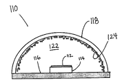
도 2를 참조하면, 본 발명의 일실시형태의 단면도가 도시되어 있다. 이 실시형태에서, LED 패키지는 도면부호 110이 부여되고 서브마운트(submount)(114)에 설치된 LED 칩(112)을 포함하고, 서브마운트는 반사기(116) 위에 차례로 설치된다. 여기서 사용된 "반사기(reflector)"는 LED 패키지의 바닥 위의 어떠한 표면 뿐만 아니라 예를 들면 히트 싱크(heat sink) 등의 LED 칩을 지지하는 다른 구조들을 포함하는 것을 의미한다. 투명물질로 만들어진 렌즈(118)는 칩(112)과 서브마운트(114)와 반사기(116)를 둘러싸고 있다. 렌즈와 칩(112) 사이의 충전 공간(122)은 일반적으로 에폭시 또는 다른 투명물질이다. 인광물질입자를 포함하는 인광물질층(124)은 렌즈(118)의 내측면 또는 외측면에 적용된다. 코팅은 인광물질 코팅이 핸들링 등에 의해 대치되는 것을 방지하기 위해 렌즈의 내측면에 코팅되는 것이 바람직하다. 인광물질코팅의 두께는 LED 칩에 의해 방출된 방사선의 적어도 일부를 다른 파장으로 변환하는데 충분하게 된다. 이것은 6-200㎛이고, 바람직한 두께는 20-30㎛이다. 2, a cross-sectional view of one embodiment of the present invention is shown. In this embodiment, the LED package includes an
LED 칩(112)은 통상적인 UV 또는 청색광 LED로 될 수 있다. 그러한 LEDs는 알려져 있고 사파이어, 알루미나 또는 단일결정 SiC 기판 상에 에피택셜하게 성장한 InGaN 또는 AlGaN 층으로 이루어져 있다. 바람직한 LED 칩은 200-480 nm의 범위에서 일차 방출을 갖는다. 그리고, 인광물질층(124)은 UV 또는 청색 방사선을 흡수할 수 있고 LED 칩에 의해 방출된 방사선, 일루미네이션을 위한 가시 백색 또는 근-백색광 단독으로 또는 조합하여 생성할 수 있는 하나 이상의 적합한 형광 인광물질을 포함한다. 본 발명에 사용되기 위한 적합한 인광물질은 특별히 제한되지는 않지만 Y3Al5O2:Ce(YAG:Ce), Tb3Al4.9O12:Ce (TAG:Ce), 및 Sr4Al14O25:Ce (SAE:Ce)를 포함한다. 다른 백색광 생성 인광물질도 또한 적합하다. 인광물질 입자들의 사이즈는 임계적이지는 않지만, 실시예에 의해 3-30㎛로 될 수 있다.
렌즈(118)는 인광물질과 LED 칩에 의해 방출된 방사선에 실질적으로 투명한 물질로 만들어질 수 있다. 그러므로, 방출된 방사선의 파장에 의존하여 렌즈는 제한되는 것은 아니지만 유리, 에폭시, 플라스틱, 열경화성 또는 열가소성 수지, 또는 당해 기술분야에 알려진 다른 모든 타입의 LED 캡슐화 물질을 포함한다.
에폭시 또는 다른 충전 물질로 분산되는 것 보다 렌즈(118)의 내측면에 인광물질 코팅(124)을 제공하는 것이 LED 방출의 보다 더 균일하고 효율적인 변한을 제공한다. 하나의 장점은 콘트롤된 두께의 균일한 코팅이 적용된다는 것이다. 이러한 하나의 이점은 코팅 두께가 최적 변환 효율과 UV 방출 칩이 사용되는 경우 최소량의 인광물질을 사용하는 콘트롤을 통한 UV 블리드를 위해 정밀하게 콘트롤될 수 있는 것이다. 이것은 종래 장치에서 인광물질의 불균일 분산으로부터 초래되는 컬러 링(color ring)의 입사 없이 균일한 발광에 도움을 준다. 다른 이점은 인광물질이 LED에 의해 발생된 열을 제거하고 변환효율을 증가시키는 것이다. 물론, 인광물질층은 렌즈물질 안쪽에 위치되거나 그 위에 위치된 다른 물질의 코팅을 갖고, 그러한 배열은 본 발명에 의해 고려될 수 있다.Providing the
제한하고자 의도된 것은 아니지만, 인광물질 코팅은 예를 들면 균일한 두께의 코팅을 제공할 수 있는 분무 코팅, 롤러 코팅, 메니스커스 또는 딥 코팅, 스탬핑, 스크리닝, 디스펜싱, 롤링, 브러싱 또는 스프레잉 또는 기타 다른 방법에 의해 적용될 수 있다. 바람직한 인광물질 적용방법은 분무코팅에 의한 방법이다.While not intended to be limiting, phosphor coatings may, for example, spray coating, roller coating, meniscus or dip coating, stamping, screening, dispensing, rolling, brushing or spraying, which can provide coatings of uniform thickness. Or by other methods. Preferred phosphor application methods are by spray coating.
LED 하우징으 렌즈와 반응기 부분을 코팅하는 기술에서, 인광물질 파우더는 바인더와 용매와 함께 슬러리 내에서 교반된다. 적합한 바인더는 제한되지는 않지만 실리콘, 에폭시, 열가소성 수지, 아크릴, 폴리이미드 및 이들의 혼합물을 포함한다. 적합한 용매는 제한되는 것은 아니지만 톨루엔, 메틸에틸케톤(MEK), 메틸렌 클로리드, 및 아세톤 등의 낮은 비등점을 갖는 용매를 포함한다. 슬러리에서 각 성분들의 양은 임계적은 아니지만, LED 방사선의 효율적인 변환을 위한 충분한 농도의 인광물질 입자를 함유하는 동안 렌즈에 쉽게 적용되는 슬러리를 생성하기 위해 선택된다. 예시된 슬러리는 6㎛ 인광물질 2중량부, 실리콘 1.2중량부 및 MEK 1중량부를 사용하여 만들어질 수 있다. 적합한 실리콘은 GE XE 5844이다.In the technique of coating the lens and reactor portions with the LED housing, the phosphor powder is stirred in the slurry together with the binder and solvent. Suitable binders include, but are not limited to, silicones, epoxies, thermoplastics, acrylics, polyimides, and mixtures thereof. Suitable solvents include, but are not limited to, solvents having low boiling points such as toluene, methylethylketone (MEK), methylene chloride, and acetone. The amount of each component in the slurry is not critical, but is chosen to produce a slurry that is easily applied to the lens while containing sufficient concentration of phosphor particles for efficient conversion of LED radiation. The illustrated slurry can be made using 2 parts by weight of 6 μm phosphor, 1.2 parts by weight of silicon and 1 part by weight of MEK. Suitable silicone is GE XE 5844.
슬러리는 이어서 렌즈의 표면에 적용된다. 그 다음에 코팅된 렌즈는 굽거나 가열되거나 그렇지 않으면 용매를 제거하고 바인더를 경화하기 위해 처리된다. 여기서 사용된 바와 같이, 용어 "경화"는 바인더의 실제 경화 또는 크로스링킹(crosslinking) 뿐만 아니라 인광물질 입자들이 바인더의 고체화 또는 경화에 기인하여 바인더에 상대적으로 고정되는 바인더에 화학적 및/또는 물리적 변화를 나타내는 것을 의미한다. The slurry is then applied to the surface of the lens. The coated lens is then baked, heated or otherwise processed to remove solvent and cure the binder. As used herein, the term "curing" refers not only to the actual curing or crosslinking of the binder, but also to chemical and / or physical changes in the binder where the phosphor particles are fixed relative to the binder due to the solidification or curing of the binder. It means to indicate.
위에 언급된 바와 같이, 슬러리는 적합한 방법을 통해 렌즈에 적용될 수 있다. 바람직한 방법에서, 슬러리는 분무 코팅에 의해 적용된다. 이 방법에서, 슬러리는 적절한 에어 브러시(air brush)의 저장용기(reservior)를 채우는데 사용된다. 그리고 나서 슬러리는 가압 분무총을 사용하여 렌즈상에 분무되고, 이 렌즈는 예비가열되고 용매의 비등온도 이상의 높은 온도에서, 예를 들면 약 110℃에서 열판위에 유지한다. 그 부분은 연속적인 패스(pass)를 만드는 것에 의해 분무되고, 이것은 패스당 약 1/2초로 행해진다. 슬러리는 접촉으로 건조되고 균일한 코팅이 얻어진다. 대략 4층 두께(6 ㎛ 사이즈 인광물질 입자를 사용하는 약 20-30㎛) 코팅이 35-40 패스로 렌즈 상에 달성된다. 렌즈는 바인더를 경화하기 위해 구워진다. 코팅 LED에 대한 이러한 접근이 일반적인 일루미네이션을 위한 LED's에 사용되는 것이 계획된다. 필요하면, 투명물질의 이차코팅이 인광물질을 보호하기 위해 인광물질층 위에 추가되거나 또는 광 추출을 돕기 위해 오버코팅(overcoating)을 제공할 수 있다. As mentioned above, the slurry can be applied to the lens via a suitable method. In a preferred method, the slurry is applied by spray coating. In this method, the slurry is used to fill the reservoir of a suitable air brush. The slurry is then sprayed onto the lens using a pressurized spray gun, which is preheated and held on a hotplate at a temperature above the boiling temperature of the solvent, for example at about 110 ° C. That portion is sprayed by making a continuous pass, which is done at about 1/2 second per pass. The slurry is dried by contact to obtain a uniform coating. Approximately four layer thickness (about 20-30 μm using 6 μm size phosphor particles) coating is achieved on the lens in 35-40 passes. The lens is baked to cure the binder. It is envisioned that this approach to coated LEDs will be used for LED's for general illumination. If desired, a secondary coating of transparent material may be added over the phosphor layer to protect the phosphor or provide overcoating to aid in light extraction.
광 출력의 현저한 개선이 인광물질이 슬러리에 묻히고 칩 주위에 불균일하게 적용된 통상의 코팅방법으로 YAG 인광물질이 있는 청색 LED's를 사용하여 달성되었다. LED 칩을 둘러싸는 렌즈와 관계가 먼 많은 다른 방법이 있다. 이들은 본 발명의 범위 내에 속한다. Significant improvements in light output have been achieved using blue LED's with YAG phosphors in a conventional coating method where the phosphors are buried in the slurry and applied unevenly around the chip. There are many other ways apart from the lens surrounding the LED chip. These are within the scope of the present invention.
바람직한 일실시형태에서, 렌즈는 칩의 한쪽 길이("L")의 적어도 2-3배인 반경을 갖는다. 이 배열은 그러한 렌즈에 적용된 코팅을 벗어나 발생되거나 반사된 방사선이 흡수 및 손실되는 칩 또는 다른 비코팅 영역 보다는 오히려 재투과되는 코팅의 다른 부분을 스트라이크할 것 같은 가망성을 증가시킨다. In one preferred embodiment, the lens has a radius that is at least 2-3 times one length ("L") of the chip. This arrangement increases the likelihood of striking other parts of the coating that are retransmitted rather than the chip or other uncoated areas where radiation generated or reflected outside of the coating applied to such lenses is absorbed and lost.
도 3에 도시된 제2 실시형태에서, LED 패키지는 도면부호 210이 부여되고 서브마운트(submount)(214)에 설치된 LED 칩(212)을 포함하고, 서브마운트는 반사기(216) 위에 차례로 설치된다.In the second embodiment shown in FIG. 3, the LED package includes an
렌즈(218)는 칩(212)과 서브마운트(214)와 반사기(216)를 둘러싸고 있다. 렌즈와 칩(212) 사이의 충전 공간(222)은 일반적으로 에폭시 또는 다른 투명물질이다. 효율을 더 개선하기 위해, 인광물질입자를 포함하는 인광물질코팅(224)은 렌즈(218)의 내측면(226)에 적용되고 반사기(216)의 상부면(218)에 적용된다. 패키지의 바닥로서 생각되는 반사기의 상부면은 먼저 알루미나, 티타니아 등의 높은 유전 파우더 같은 반사층(240)으로 코팅되는 것이 바람직하다. 바람직한 반사물질은 Al2O3 이다. 인광물질층(224)은 반사기의 상부에 있는 반사층(240) 위에 위치된다. 반사층(240)의 사용은 이 표면상의 인광물질층(224)을 투과하는 방사선(242)을 반사하는데 제공된다. 투명렌즈(218)를 인광물질층(224)으로 코팅하는 대신에, 인광물질이 투명 반구체를 포함하는 물질 내에 밀접하게 분산될 수도 있다.
반사기(216) 상의 반사층(240) 위쪽의 인광물질층(224)은 상대적으로 두꺼운, 즉 >5 파우더 층이 바람직하지만, 반구체의 곡면 상부 상의 인광물질층은 원하는 색을 얻기 위해 그리고 그 위에 입사되는 모든 방사선을 흡수하기 우해 조정될 수 있다. 일반적으로 반구체의 상부의 인광물질층은 청색 방사선의 일부가 방출되기 위해 청색 발광 칩의 경우에 1-4층 두께 범위가 될 것이다. UV 칩의 경우에 반구체상의 인광물질 코팅 층은 칩에 의해 방출된 UV 방사선의 대부분을 흡수하기 위해 4-8층 두께가 된다.The
도 3에 도시된 바와 같이, 칩에서 나오는 방사선(242)은 먼저 반구체의 인광물질 코팅 표면을 스트라이크(strike)하지 않고 구조를 벗어나지 못하게 한다. 또한, 전체 인광물질 코팅 표면적은 발광 칩의 표면적보다 더 크고, 바람직하게는 LED 칩의 흡수부분의 노출 표면적의 적어도 10배이다. 여기서 사용된 바와 같이, LED의 흡수부분의 노출 표면적은 반사층 및/또는 인광물질층으로 커버되지 않은 서브마운트의 노출 표면 뿐만 아니라 LED 칩의 노출 표면을 포함한다.As shown in FIG. 3, the
그러한 배열에서, 반구체 내로 산란되는 상당량의 청색 또는 UV 방사선이 있지만, 산만하게 산란되는 거의 모든 이러한 방사선은 칩 또는 서브마운트보다는 오히려 인광물질 코팅의 다른 부분을 스트라이크한다. 인광물질 코팅에 의해 발생된 대부분의 가시광선은 반구체 내로 향하게 된다. 또한, 금속성 반사기도 없고 노출된 리드 구조(lead structure)도 없다. 이러한 기하구조의 중요한 특성은 LED 칩(212)을 제외한 모든 것이 커버된 인광물질이고 반구체의 인광물질 표면적은 LED의 흡수 부분의 표면적 보다 훨씬 더 크고, 바람직하게는 >10배 이다. 그러므로, 반구체로 되돌아가는 거의 모든 방사선은 다른 인광물질 코팅영역을 스크라이크할 것이고 인광물질에 의해 반사 또는 흡수되고 재투과된다. 여기에 개시된 실시형태들은 70% 보다 큰 효율을 갖게 계산되고, 대부분의 경우 100%에 근접한다. In such an arrangement, there is a significant amount of blue or UV radiation scattered into the hemisphere, but almost all such scattered radiation strikes other portions of the phosphor coating rather than chips or submounts. Most of the visible light generated by the phosphor coating is directed into the hemisphere. There is also no metallic reflector and no exposed lead structure. An important characteristic of this geometry is that all but the
표 1에서 이런 디자인의 효율은 몇몇 표준 LED 패키지 기하구조와 비교된다. 이들 비교는 컴퓨터 시뮬레이션을 사용하여 하였다. 컴퓨터 시뮬레이션은 이하에 설명된 플럭스(flux) 모델이다. 그것은 모든 방사선 플럭스를 고려하고 주어진 표면 상에 입사하는 방사선의 양이 그 면적에 비례하도록 모든 것이 분산된다고 생각한다. 표 1에 나타낸 것처럼 위에 설명된 기하구조는 100%의 패키지 효율을 제공한다.In Table 1, the efficiency of this design is compared with some standard LED package geometries. These comparisons were made using computer simulations. Computer simulation is a flux model described below. It takes into account all radiation fluxes and thinks that everything is dispersed so that the amount of radiation incident on a given surface is proportional to its area. As shown in Table 1, the geometry described above provides 100% package efficiency.
표 1. 본 발명에 개시된 실시형태와 인광물질 코팅 LED's의 표준 배열의 계산된 패키지 효율의 비교 Table 1.Comparison of the calculated package efficiency of a standard arrangement of phosphor coated LED's with an embodiment disclosed herein
도 4는 같은 원리로 오퍼레이팅하는 제2 실시형태를 나타낸다. 여기서 LED칩(312)은 히트 싱크로서 제공되는 페데스탈(pedestal)(314)에 장착된다. 그러나 칩(312)은 성형된 구체(318)의 중심에 위치된다. 인광물질층(미도시)은 구체(318)의 내측면(320)에 코팅되거나, 또는 구체 내에 밀접하게 분산된다. 이런 디자인에서, LED는 모든 방향으로 균일하게 방사된다. 인광물질 코팅에 의해 발생되고 구체내로 다시 산란된 청색/UV 방사선과 가시 방사선은 칩(312)이나 페데스탈(314)을 스트라이크하기보다는 오히려 다른 인광물질 코팅 표면을 스트라이크하는 것이 명백하다. 이들 광 흡수 구조는 분산 방사선에 대한 작은 타겟이다. 표 1에서 보는 바와 같이, 패키지 효율은 이 배열에 대해 100%에 가깝다. SiC 기판 상의 LED 구조에 대한 낮은 패키지 효율은 Al2O3 기판과 비교할 때 SiC 기판에 의한 LED 방사선의 더 큰 흡수에 기인한다. 4 shows a second embodiment operating on the same principle. Here the
앞의 실시형태로부터, 인광물질 코팅의 특정 형태는 LED 칩을 가능한 한 완전히 둘러싸고 있고 코팅으로부터 산란된 방사선이 칩이나 칩구조를 스트라이크하지 않도록 칩으로부터 충분한 거리 (예, 인광물질 코팅 표면이 칩의 노출 표면적의 10배 보다 더 큰 표면적을 갖는 거리)를 두고 있는 한 중요하지 않다. 본 발명은 여기에 설명된 실시형태에 제한되는 것이 아니라 그러한 모든 코팅 형상을 포함하는 것이고, 바람직하게는 표면을 덮는 인광물질은 LED의 흡수부분의 노출영역의 약 10배 또는 그보다 더 크다. 그러므로, 인광물질이 코팅된 렌즈는 반구체 또는 구체에 한정되지 않고, 다른 기하학적 형상, 바람직하게는 LED의 흡수부분의 노출영역의 약 10배 또는 그보다 더 큰 인광물질 코팅 표면적을 갖는 기하학적 형상을 포함한다. From the foregoing embodiments, certain forms of phosphor coatings surround the LED chip as completely as possible and provide sufficient distance from the chip (eg, the phosphor coating surface is exposed to the chip so that the radiation scattered from the coating does not strike the chip or chip structure). As long as the surface area is greater than 10 times the surface area). The invention is not limited to the embodiments described herein but includes all such coating shapes, preferably the phosphor covering the surface is about 10 times or greater than the exposed area of the absorbing portion of the LED. Therefore, phosphor coated lenses are not limited to hemispheres or spheres, but include other geometries, preferably geometries having a phosphor coating surface area of about 10 times or greater than the exposed area of the absorbing portion of the LED. do.
본 발명은 또한 그렇게 이상적이지 않은 기하구조를 커버하고자 하는 것이고 100% 패키지 효율의 완전한 이점을 주지는 않고 코팅 표면이 칩의 방출 영역의 적어도 10배가 되도록 디자인된 원격 인광물질 코팅의 원리를 이용하는 것이다. 예를 들면 도 5는 통상적인 표면 장착 LED의 개략을 나타낸다. 이 배열에서, LED 칩(412과 서브마운트(414)는 반응기 컵(416)에 장착된다. 반응기와 렌즈 사이의 광학 매체에 임의로 묻힌 인광물질을 가지는 통상적인 디자인과는 달리, 인광물질 코팅은 투명렌즈(418)에 하나의 층으로서 적용된다. 인광물질 코팅은 칩(412)과 떨어져 있고 LED의 흡수 부분의 노출영역의 약 >10배를 갖는 표면 상에 있다. 인광물질코팅이 적용된 렌즈(418)의 표면은 칩의 표면적의 10배 보다 작은 표면적을 갖는다. 그러나 더 많은 방사선이 방출되어 부딪치고 칩에 의해 흡수되므로 어셈블리의 패키지 효율은 감소된다. 다시, 제2 렌즈(430)가 보호를 위해 인광물질 코팅 렌즈 위에 장착될 수 있다.The invention also seeks to cover a geometry that is not so ideal and utilizes the principle of a remote phosphor coating designed so that the coating surface is at least 10 times the emitting area of the chip without giving the full advantage of 100% package efficiency. For example, FIG. 5 shows an overview of a typical surface mount LED. In this arrangement, the
인광물질 코팅으로부터 산란되어 오는 대부분의 UV 또는 청색 방사선과 가시 방사선은 반사기 컵(416)이나 다른 인광물질 표면에 부딪친다. 단지 상대적으로 작은 양이 광 흡수 칩과 서브마운트에 부딪친다. 이런 디자인에서, 반사기 컵(416)이 매우 높은 반사성 물질, 예를 들면 미세하게 분할된 알루미나 또는 티타니아 같은 고순도 무기 파우더 또는 >95% 반사율을 갖는 증착 및 보호 은 코팅으로 만들어지는 것이 중요하다. 반사기 컵(416)은 인광물질로 코팅되거나 또는 코팅되지 않아도 된다. 표 1은 면적 27㎟의 인광물질 코팅 렌즈를 이용하는 은 반사기 컵에서 서브마운트 상에 1.6㎟의 면적을 갖는 특정 LED의 시뮬레이트된 성능을 나타낸다. Most of the UV or blue and visible radiation scattered from the phosphor coating hits the
도 6과 7에 나타낸 바와 같이, 본 발명은 또한 다중 LED 칩을 포함하는 시스템에 적용된 원격 인광물질 코팅의 개념이 개시되어 있다. 다중 청색 또는 UV 발광 LED's가 단일 반사 전기적 상호연결 보드 또는 다른 구조 상에 장착될 수 있다. 인광물질 코팅 표면은 단일 LED가 아니라 LED's 세트 전체를 둘러싸는데 사용된다. 인광물질 코팅 표면은 단독으로 또는 LED's 세트를 둘러싸는 다른 높은 반사 표면과 조합으로 사용된다. 그러한 구조의 두 예는 도 6과 7에 도시되어 있다. 하나는 다운라이트(downlight)로 사용되는 파워 모듈(500)이다. 다른 하나는 인광물질 코팅 패널 뒤에 장착된 많은 LED's가 있는 패널 램프(600)이다. 그러한 많은 배열은 인광물질 표면적이 LED의 흡수부분의 노출된 면적의 10배인 것이 제공되는 것이 명백하다. As shown in Figures 6 and 7, the present invention also discloses the concept of a remote phosphor coating applied to a system comprising multiple LED chips. Multiple blue or UV emitting LED's may be mounted on a single reflective electrical interconnect board or other structure. The phosphor coated surface is used to surround the entire set of LED's, not a single LED. The phosphor coating surface is used alone or in combination with other high reflective surfaces surrounding the LED's set. Two examples of such structures are shown in FIGS. 6 and 7. One is a
위에 설명된 바와 같이, 이들 실시형태중 어느 것이든지 LED 칩과 인광물질 코팅 렌즈 사이의 에폭시 또는 다른 투명 필러(filler)를 포함한다. 캡슐화제 또는 투명 필터의 굴절률이 다이(die)와 렌즈의 굴절률의 기하평균에 아주 매치될 때, 바람직하게는 이 값의 약 20% 내, 더 바람직하게는 10% 이내일 때, 보다 효율적인 광의 추출이 실현될 수 있다. 이것은 램프에서 내부 반사의 양을 감소시킨다. 그러므로 약 1.5의 굴절률을 갖는 렌즈가 있는 약 2.7의 굴절률을 갖는 GaN LED 칩의 경우에, 필러는 약 2.1의 굴절률을 갖는 것이 바람직하다. 굴절률이 약 1.7인 사파이어 서브마운트 상에 GaN 반도체 같은 다른 굴절률을 갖는 둘이상의 물질을 갖는 LED 칩의 경우에, 캡슐화제의 굴절률은 바람직하게는 렌즈와 둘 중 더 높은 것의 기하평균에 매치된다. 더 양호한 광추출은 스핀-온 글래스(spin-on glass)(SOG) 또는 다른 높은 굴절률 물질 같은 에폭시보다 더 높은 굴절률을 갖는 갭슐화제로 달성될 수 있다. As described above, either of these embodiments includes an epoxy or other transparent filler between the LED chip and the phosphor coated lens. More efficient extraction of light when the refractive index of the encapsulating agent or transparent filter matches the geometric mean of the refractive index of the die and the lens, preferably within about 20% of this value, more preferably within 10% This can be realized. This reduces the amount of internal reflection in the lamp. Therefore, in the case of a GaN LED chip having a refractive index of about 2.7 with a lens having a refractive index of about 1.5, the filler preferably has a refractive index of about 2.1. For LED chips having two or more materials with different refractive indices, such as GaN semiconductors, on a sapphire submount with a refractive index of about 1.7, the refractive index of the encapsulant preferably matches the geometric mean of the higher of the two. Better light extraction can be achieved with an encapsulant having a higher refractive index than epoxy, such as spin-on glass (SOG) or other high refractive index materials.
상기 실시형태 중 어느 것이든지 생성 LED 패키지의 효율을 개선하기 위해 하나 이상의 밴드 패스 필터를 구비할 수 있다. 그러므로, 도 9에 나타낸 바와 같이, 일실시형태에서, 청색 LED 소스를 위한 렌즈(718)는 제1 밴드 패스 필터(750)를 포함하여 나타나 있다. 밴드 패스 필터는 인광물질층(724)과 LED(미도시) 사이에 위치된다. 밴드 패스 필터는 인광물질층에서 방출된 광(754)이 바깥쪽으로 반사되는 동안 청색 LED 소스로부터 입사광이 패스되도록 선택된다.Any of the above embodiments may be provided with one or more band pass filters to improve the efficiency of the resulting LED package. Therefore, as shown in FIG. 9, in one embodiment, the
도 10에 나타낸 실시형태에서, 두 밴드 패스 필터가 UV LED 소스 패키지에 제공된다. 이 실시형태에서, 제1 밴드패스필터(850)가 인광물질층(824)과 렌즈(818)에 인접한 LED소스(미도시) 사이에 위치딘다. 제1 밴드패스필터는 인광물질층에서 방출된 광(854)이 반사하는 동안 LED 유래의 UV광(852)을 투사하기 위해 작용한다. 제2 밴드패스필터(856)는 인광물질층에서 방출된 광(854)이 패스하는 동안 LED 유래의 UV광(852)을 반사한다. 이 배열은 가시광을 투과하게 하는 동안 패키지로부터 해로운 UV방사선의 투과를 방지한다. In the embodiment shown in FIG. 10, two band pass filters are provided in a UV LED source package. In this embodiment, a
도 11에서 보는 바와 같이, 마이크로 또는 매크로 렌즈(960)의 어레이(array)가 방출 방사선(952 및 954)의 방사 각도, 방향 또는 세기를 콘트롤하기 위해 상기 실시형태의 어느 것이든지 렌즈의 외부표면에 형성된다. As can be seen in FIG. 11, an array of micro or macro lenses 960 can be mounted on the outer surface of the lens in any of the above embodiments to control the angle, direction, or intensity of the radiation of
표 1에 나타낸 계산결과는 도 8에 나타낸 선형 플럭스 모델을 기초로 한 것이다. 도 8은 LED 패키지의 네 면에 입사하는 9개의 플럭스(flux)를 나타낸다. 이들 플럭스는 아래의 아홉개의 선형 방정식에 의해 설명되고, 각 방정식으로 대응하는 수로 플럭스를 묘사한다. 이들 방정식은 아래와 같다:The calculation results shown in Table 1 are based on the linear flux model shown in FIG. 8 shows nine fluxes incident on four sides of the LED package. These fluxes are described by the following nine linear equations, each of which describes the corresponding channel flux. These equations are as follows:
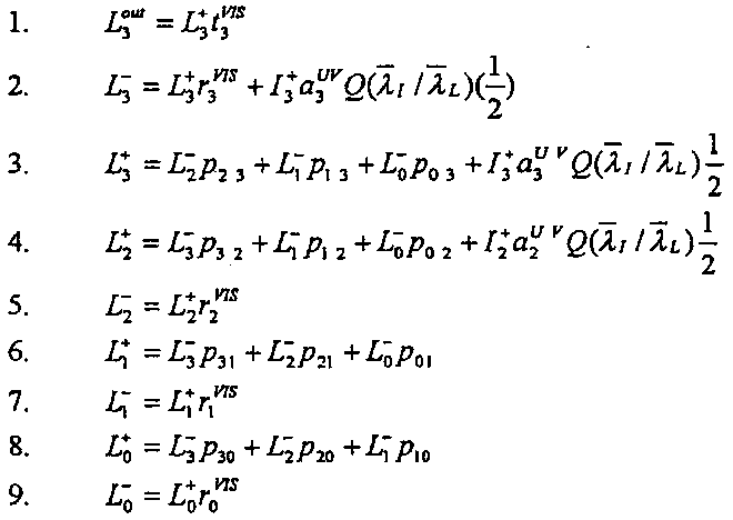
이들 표면은 다음과 같다:These surfaces are as follows:
3 = 상부 인광물질 코팅면,3 = top phosphor coated surface,
2 = 하부 인광물질 코팅면,2 = bottom phosphor coated surface,
1 = 반사기와 서브마운트, 및1 = reflector and submount, and
0 = 청색 또는 UV 방출 칩0 = blue or UV emitting chip
청색 또는 UV 플럭스를 묘사하는 9개의 다른 방정식도 있다. 청색 또는 UV 플럭스를 묘사하는 방정식은 나타내지 않았다. 그들은 양자 효율 Q 와 스톡스 이동(Stock's shift)(λi/λl)을 통해 가시 광 방정식에 결합된다. 18개의 선형방정식은 18개의 알려지지 않은, 즉 각 면을 스크라이크하는 방사선의 상대적 파워로 되고, 동시에 해결된다. There are also nine other equations describing blue or UV flux. Equations describing blue or UV flux are not shown. They are coupled to the visible light equation via quantum efficiency Q and Stock's shift (λi / λl). The 18 linear equations are 18 unknowns, i.e. the relative power of the radiation that strikes each side, and are solved simultaneously.
p 값은 한 표면 유래의 방사선이 다른 표면을 스트라이크할 확률이다. 도 1에 나타낸 계산에서, 이들은 표면적의 비가 되도록 취해졌다. Q는 인광물질의 양자효율이다. λ는 청색 또는 UV 칩 방사선의 평균파장 또는 인광물질의 가시방사의 평균파장이다.The p value is the probability that radiation from one surface strikes another surface. In the calculations shown in FIG. 1, they were taken to have a ratio of the surface areas. Q is the quantum efficiency of the phosphor. λ is the average wavelength of blue or UV chip radiation or the average wavelength of visible radiation of the phosphor.
요구된 다른 파라미터는 다른 물질 표면의 반사율과 흡수율이다. 이들은 편람값으로 얻어지거나 또는 알려진 방법을 사용하여 직접 측정된다. 칩의 반사율에 대한 값이 없고 그래서 이들은 각 칩이 반도체층과 기판으로 구성된 것으로 가정하여 계산되었다. 칩 상의 모든 방사선 입사는 정상으로 가정되었고 플립-칩 디자인의 기판상의 입사와 회절효과는 무시되었다. 칩의 반사율에 대한 표면은 다음과 같다: Other parameters required are the reflectance and the absorbance of other material surfaces. These are obtained as handbook values or measured directly using known methods. There is no value for the reflectivity of the chips and so they were calculated assuming that each chip consists of a semiconductor layer and a substrate. All radiation incidents on the chip were assumed to be normal and the incident and diffraction effects on the substrate of the flip-chip design were ignored. The surface for the reflectance of the chip is as follows:
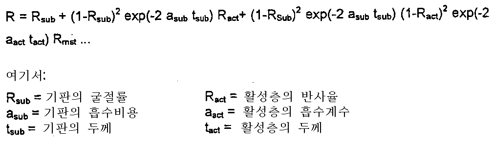
알려지거나 개산된 값은 굴절율, 흡수계수 및 두께에 대해 사용되었다. 그러므로, Known or estimated values were used for refractive index, absorption coefficient and thickness. therefore,
![]()
![]()
본 발명은 바람직한 실시형태와 관련하여 설명되었다. 당해 기술분야에 통상의 지식을 가진 자가 전술한 상세한 설명을 기초로 많은 변경 및 변형을 할 수 있음은 자명하다. 본 발명은 본 발명의 기술사상과 정신을 벗어나지 않는 범위내에서 이루어지는 그러한 모든 변형 및 변경을 포함한다.The present invention has been described in connection with preferred embodiments. It will be apparent to those skilled in the art that many modifications and variations can be made based on the foregoing detailed description. The present invention includes all such modifications and changes made without departing from the spirit and spirit of the invention.
Claims (49)
Applications Claiming Priority (2)
| Application Number | Priority Date | Filing Date | Title |
|---|---|---|---|
| US40742602P | 2002-08-30 | 2002-08-30 | |
| US60/407,426 | 2002-08-30 |
Publications (2)
| Publication Number | Publication Date |
|---|---|
| KR20050046742A KR20050046742A (en) | 2005-05-18 |
| KR100622209B1 true KR100622209B1 (en) | 2006-09-19 |
Family
ID=31978482
Family Applications (1)
| Application Number | Title | Priority Date | Filing Date |
|---|---|---|---|
| KR1020057003453A Expired - Fee Related KR100622209B1 (en) | 2002-08-30 | 2003-08-29 | Coated led with improved efficiency |
Country Status (10)
| Country | Link |
|---|---|
| US (1) | US7479662B2 (en) |
| EP (1) | EP1540746B1 (en) |
| JP (1) | JP2005537651A (en) |
| KR (1) | KR100622209B1 (en) |
| CN (1) | CN100468791C (en) |
| AT (1) | ATE448571T1 (en) |
| AU (1) | AU2003270052B2 (en) |
| DE (1) | DE60330023D1 (en) |
| ES (1) | ES2335878T3 (en) |
| WO (1) | WO2004021461A2 (en) |
Families Citing this family (307)
| Publication number | Priority date | Publication date | Assignee | Title |
|---|---|---|---|---|
| US6600175B1 (en) | 1996-03-26 | 2003-07-29 | Advanced Technology Materials, Inc. | Solid state white light emitter and display using same |
| US10340424B2 (en) | 2002-08-30 | 2019-07-02 | GE Lighting Solutions, LLC | Light emitting diode component |
| US7224000B2 (en) * | 2002-08-30 | 2007-05-29 | Lumination, Llc | Light emitting diode component |
| US7118438B2 (en) | 2003-01-27 | 2006-10-10 | 3M Innovative Properties Company | Methods of making phosphor based light sources having an interference reflector |
| US7245072B2 (en) | 2003-01-27 | 2007-07-17 | 3M Innovative Properties Company | Phosphor based light sources having a polymeric long pass reflector |
| EP1588434A2 (en) | 2003-01-27 | 2005-10-26 | 3M Innovative Properties Company | Phosphor based light source component and method of making |
| US7312560B2 (en) | 2003-01-27 | 2007-12-25 | 3M Innovative Properties | Phosphor based light sources having a non-planar long pass reflector and method of making |
| US20040159900A1 (en) | 2003-01-27 | 2004-08-19 | 3M Innovative Properties Company | Phosphor based light sources having front illumination |
| US7091661B2 (en) | 2003-01-27 | 2006-08-15 | 3M Innovative Properties Company | Phosphor based light sources having a reflective polarizer |
| US20040145289A1 (en) | 2003-01-27 | 2004-07-29 | 3M Innovative Properties Company | Phosphor based light sources having a non-planar short pass reflector and method of making |
| US7091653B2 (en) | 2003-01-27 | 2006-08-15 | 3M Innovative Properties Company | Phosphor based light sources having a non-planar long pass reflector |
| US7423296B2 (en) * | 2003-02-26 | 2008-09-09 | Avago Technologies Ecbu Ip Pte Ltd | Apparatus for producing a spectrally-shifted light output from a light emitting device utilizing thin-film luminescent layers |
| US7084434B2 (en) * | 2003-04-15 | 2006-08-01 | Luminus Devices, Inc. | Uniform color phosphor-coated light-emitting diode |
| US7005679B2 (en) * | 2003-05-01 | 2006-02-28 | Cree, Inc. | Multiple component solid state white light |
| US7247986B2 (en) * | 2003-06-10 | 2007-07-24 | Samsung Sdi. Co., Ltd. | Organic electro luminescent display and method for fabricating the same |
| US7329024B2 (en) | 2003-09-22 | 2008-02-12 | Permlight Products, Inc. | Lighting apparatus |
| JP3837588B2 (en) | 2003-11-26 | 2006-10-25 | 独立行政法人物質・材料研究機構 | Phosphors and light emitting devices using phosphors |
| US8174036B2 (en) * | 2003-12-30 | 2012-05-08 | Osram Opto Semiconductors Gmbh | Lighting device |
| US7517728B2 (en) | 2004-03-31 | 2009-04-14 | Cree, Inc. | Semiconductor light emitting devices including a luminescent conversion element |
| JP4317478B2 (en) * | 2004-03-31 | 2009-08-19 | 三菱化学株式会社 | Phosphor-type light emitting device and endoscope device using the same as an illumination source |
| US7724440B2 (en) | 2004-04-23 | 2010-05-25 | Light Prescriptions Innovators, Llc | Combining outputs of different light sources |
| CN101076744B (en) | 2004-04-23 | 2010-05-12 | 光处方革新有限公司 | Optical manifold for light emitting diodes |
| US6956247B1 (en) * | 2004-05-26 | 2005-10-18 | Lumileds Lighting U.S., Llc | Semiconductor light emitting device including photonic band gap material and luminescent material |
| US7781789B2 (en) * | 2006-11-15 | 2010-08-24 | The Regents Of The University Of California | Transparent mirrorless light emitting diode |
| US7070300B2 (en) * | 2004-06-04 | 2006-07-04 | Philips Lumileds Lighting Company, Llc | Remote wavelength conversion in an illumination device |
| WO2006023149A2 (en) * | 2004-07-08 | 2006-03-02 | Color Kinetics Incorporated | Led package methods and systems |
| US7201495B2 (en) * | 2004-08-03 | 2007-04-10 | Philips Lumileds Lighting Company, Llc | Semiconductor light emitting device package with cover with flexible portion |
| US20060097385A1 (en) * | 2004-10-25 | 2006-05-11 | Negley Gerald H | Solid metal block semiconductor light emitting device mounting substrates and packages including cavities and heat sinks, and methods of packaging same |
| US7419839B2 (en) * | 2004-11-12 | 2008-09-02 | Philips Lumileds Lighting Company, Llc | Bonding an optical element to a light emitting device |
| EP1825719B1 (en) * | 2004-12-09 | 2011-06-01 | Koninklijke Philips Electronics N.V. | Illumination system |
| RU2359362C2 (en) * | 2004-12-22 | 2009-06-20 | Сеул Семикондактор Ко., Лтд. | Light-emitting device |
| TWI248218B (en) * | 2004-12-31 | 2006-01-21 | Ind Tech Res Inst | Light-emitting diode package structure and fabrication method thereof |
| US20060171152A1 (en) | 2005-01-20 | 2006-08-03 | Toyoda Gosei Co., Ltd. | Light emitting device and method of making the same |
| KR101139891B1 (en) | 2005-01-31 | 2012-04-27 | 렌슬러 폴리테크닉 인스티튜트 | Light emitting diode device having diffusedly reflective surface |
| EP1686630A3 (en) * | 2005-01-31 | 2009-03-04 | Samsung Electronics Co., Ltd. | Led device having diffuse reflective surface |
| US7497973B2 (en) * | 2005-02-02 | 2009-03-03 | Lumination Llc | Red line emitting phosphor materials for use in LED applications |
| JP2006278567A (en) * | 2005-03-28 | 2006-10-12 | Matsushita Electric Works Ltd | LED unit |
| CN100409462C (en) * | 2005-05-26 | 2008-08-06 | 陈隆建 | Reflection type white light emitting diode excited by fluorescent powder |
| US7319246B2 (en) | 2005-06-23 | 2008-01-15 | Lumination Llc | Luminescent sheet covering for LEDs |
| KR100757196B1 (en) * | 2005-08-01 | 2007-09-07 | 서울반도체 주식회사 | Light emitting device having a silicon lens |
| US20070195534A1 (en) * | 2005-08-19 | 2007-08-23 | Ha Duk S | Side emitting lens, light emitting device using the side emitting lens, mold assembly for preparing the side emitting lens and method for preparing the side emitting lens |
| CN100405621C (en) * | 2005-09-29 | 2008-07-23 | 上海乐金广电电子有限公司 | High-output white light source and its production |
| CN100414727C (en) * | 2005-11-04 | 2008-08-27 | 江苏日月照明电器有限公司 | A method for controlling the coating thickness of white light LED phosphor powder |
| EP1969647A4 (en) * | 2005-12-08 | 2012-08-01 | Univ California | LUMINESCENT DIODE (LED) WITH HIGH EFFICIENCY |
| US7375379B2 (en) * | 2005-12-19 | 2008-05-20 | Philips Limileds Lighting Company, Llc | Light-emitting device |
| US20070200118A1 (en) * | 2005-12-21 | 2007-08-30 | Epstein Kenneth A | Led light confinement element |
| JP2009527071A (en) * | 2005-12-22 | 2009-07-23 | クリー エル イー ディー ライティング ソリューションズ インコーポレイテッド | Lighting device |
| KR100726970B1 (en) * | 2005-12-23 | 2007-06-14 | 한국광기술원 | Light emitting device using dichroic filter |
| JP2007180234A (en) * | 2005-12-27 | 2007-07-12 | Matsushita Electric Ind Co Ltd | Luminescent light source and lighting fixture |
| CN101385145B (en) | 2006-01-05 | 2011-06-08 | 伊鲁米特克斯公司 | Discrete optics for directing light from LEDs |
| KR100867519B1 (en) * | 2006-02-02 | 2008-11-07 | 삼성전기주식회사 | Light emitting diode module |
| DE102006005042A1 (en) * | 2006-02-03 | 2007-08-09 | Tridonic Optoelectronics Gmbh | Light-emitting device with non-activated phosphor |
| DE102006008793A1 (en) * | 2006-02-24 | 2007-09-13 | Osram Opto Semiconductors Gmbh | Electronic component |
| CN100411210C (en) * | 2006-03-03 | 2008-08-13 | 中山大学 | A kind of packaging method of white light LED |
| US8299903B2 (en) * | 2006-03-23 | 2012-10-30 | Edward H Haase | Screw-in LED light and sound bulb |
| DE102006015606A1 (en) * | 2006-04-04 | 2007-10-18 | Noctron Holding S.A. | Semiconductor lamps and light panels with such |
| USD581884S1 (en) * | 2006-04-12 | 2008-12-02 | Semi-Photonics Co., Ltd. | Light emitting diode device |
| USD582361S1 (en) * | 2006-04-12 | 2008-12-09 | Semi-Photonics Co., Ltd. | Light emitting diode device |
| US7661840B1 (en) | 2006-06-21 | 2010-02-16 | Ilight Technologies, Inc. | Lighting device with illuminated front panel |
| US8947619B2 (en) | 2006-07-06 | 2015-02-03 | Intematix Corporation | Photoluminescence color display comprising quantum dots material and a wavelength selective filter that allows passage of excitation radiation and prevents passage of light generated by photoluminescence materials |
| US20080074583A1 (en) * | 2006-07-06 | 2008-03-27 | Intematix Corporation | Photo-luminescence color liquid crystal display |
| US20080012035A1 (en) * | 2006-07-11 | 2008-01-17 | Bily Wang | LED chip package structure and method for manufacturing the same |
| WO2008082703A2 (en) * | 2006-07-31 | 2008-07-10 | 3M Innovative Properties Company | Combination camera/projector system |
| US20080036972A1 (en) * | 2006-07-31 | 2008-02-14 | 3M Innovative Properties Company | Led mosaic |
| US8075140B2 (en) * | 2006-07-31 | 2011-12-13 | 3M Innovative Properties Company | LED illumination system with polarization recycling |
| EP2050147A2 (en) * | 2006-07-31 | 2009-04-22 | 3M Innovative Properties Company | Led source with hollow collection lens |
| WO2008016905A1 (en) | 2006-07-31 | 2008-02-07 | 3M Innovative Properties Company | Optical projection subsystem |
| US20080029720A1 (en) * | 2006-08-03 | 2008-02-07 | Intematix Corporation | LED lighting arrangement including light emitting phosphor |
| CN100568554C (en) * | 2006-08-16 | 2009-12-09 | 晶元光电股份有限公司 | Light-emitting diode device and light-emitting chip |
| US7842960B2 (en) * | 2006-09-06 | 2010-11-30 | Lumination Llc | Light emitting packages and methods of making same |
| KR100835063B1 (en) | 2006-10-02 | 2008-06-03 | 삼성전기주식회사 | SURFACE LIGHT SOURCE DEVICE USING LEDs |
| US20080151143A1 (en) * | 2006-10-19 | 2008-06-26 | Intematix Corporation | Light emitting diode based backlighting for color liquid crystal displays |
| WO2008060586A2 (en) | 2006-11-15 | 2008-05-22 | The Regents Of The University Of California | Textured phosphor conversion layer light emitting diode |
| CN101617411B (en) * | 2006-11-30 | 2012-07-11 | 科锐公司 | Lighting device and lighting method |
| WO2008073435A1 (en) * | 2006-12-11 | 2008-06-19 | The Regents Of The University Of California | Lead frame for transparent and mirrorless light emitting diode |
| JP2010512662A (en) | 2006-12-11 | 2010-04-22 | ザ リージェンツ オブ ザ ユニバーシティ オブ カリフォルニア | Transparent light emitting diode |
| US8109656B1 (en) | 2007-01-12 | 2012-02-07 | Ilight Technologies, Inc. | Bulb for light-emitting diode with modified inner cavity |
| US7686478B1 (en) | 2007-01-12 | 2010-03-30 | Ilight Technologies, Inc. | Bulb for light-emitting diode with color-converting insert |
| JP5102051B2 (en) * | 2007-01-18 | 2012-12-19 | シチズン電子株式会社 | Semiconductor light emitting device |
| US20080192458A1 (en) * | 2007-02-12 | 2008-08-14 | Intematix Corporation | Light emitting diode lighting system |
| US7815341B2 (en) | 2007-02-14 | 2010-10-19 | Permlight Products, Inc. | Strip illumination device |
| KR101499269B1 (en) * | 2007-02-22 | 2015-03-09 | 크리, 인코포레이티드 | Light emitting device, light emitting method, optical filter and optical filtering method |
| US7972030B2 (en) | 2007-03-05 | 2011-07-05 | Intematix Corporation | Light emitting diode (LED) based lighting systems |
| TWI402882B (en) | 2007-03-14 | 2013-07-21 | Jenn Wei Mii | Light illuminating element |
| USD573554S1 (en) * | 2007-03-30 | 2008-07-22 | Rohm Co., Ltd. | Light emitting diode module |
| USD580892S1 (en) * | 2007-03-30 | 2008-11-18 | Rohm Co., Ltd. | Lead terminals of light emitting diode module |
| US8203260B2 (en) * | 2007-04-13 | 2012-06-19 | Intematix Corporation | Color temperature tunable white light source |
| TW200842455A (en) * | 2007-04-16 | 2008-11-01 | Chi Lin Technology Co Ltd | Light mixing and guiding device |
| US7703943B2 (en) * | 2007-05-07 | 2010-04-27 | Intematix Corporation | Color tunable light source |
| US7942556B2 (en) * | 2007-06-18 | 2011-05-17 | Xicato, Inc. | Solid state illumination device |
| TW200910654A (en) | 2007-06-27 | 2009-03-01 | Univ California | Optical designs for high-efficacy white-light emitting diodes |
| KR100919461B1 (en) * | 2007-07-09 | 2009-09-28 | 심현섭 | Luminous source transformed color temperature for a lighting device |
| US10505083B2 (en) * | 2007-07-11 | 2019-12-10 | Cree, Inc. | Coating method utilizing phosphor containment structure and devices fabricated using same |
| US7663315B1 (en) | 2007-07-24 | 2010-02-16 | Ilight Technologies, Inc. | Spherical bulb for light-emitting diode with spherical inner cavity |
| JP2009038304A (en) * | 2007-08-03 | 2009-02-19 | Stanley Electric Co Ltd | Lighting fixture |
| US20090065792A1 (en) * | 2007-09-07 | 2009-03-12 | 3M Innovative Properties Company | Method of making an led device having a dome lens |
| DE102007059548A1 (en) * | 2007-09-28 | 2009-04-02 | Osram Opto Semiconductors Gmbh | Optoelectronic component and coupling-out lens for an optoelectronic component |
| DE102007049799A1 (en) * | 2007-09-28 | 2009-04-02 | Osram Opto Semiconductors Gmbh | Optoelectronic component |
| US8783887B2 (en) | 2007-10-01 | 2014-07-22 | Intematix Corporation | Color tunable light emitting device |
| US9086213B2 (en) * | 2007-10-17 | 2015-07-21 | Xicato, Inc. | Illumination device with light emitting diodes |
| JP2009099759A (en) * | 2007-10-17 | 2009-05-07 | Fine Rubber Kenkyusho:Kk | Light emitting device |
| US7984999B2 (en) | 2007-10-17 | 2011-07-26 | Xicato, Inc. | Illumination device with light emitting diodes and moveable light adjustment member |
| US7915627B2 (en) | 2007-10-17 | 2011-03-29 | Intematix Corporation | Light emitting device with phosphor wavelength conversion |
| TWI360238B (en) | 2007-10-29 | 2012-03-11 | Epistar Corp | Photoelectric device |
| US8376577B2 (en) * | 2007-11-05 | 2013-02-19 | Xicato, Inc. | Modular solid state lighting device |
| JP5666306B2 (en) * | 2007-11-20 | 2015-02-12 | コーニンクレッカ フィリップス エヌ ヴェ | Side radiation device with wavelength conversion |
| US8368294B2 (en) * | 2007-11-30 | 2013-02-05 | Jenn-Wei Mii | Brightness improving structure of light-emitting module with an optical film surface layer |
| US8042961B2 (en) * | 2007-12-02 | 2011-10-25 | Andrew Massara | Audio lamp |
| JP2010074117A (en) * | 2007-12-07 | 2010-04-02 | Panasonic Electric Works Co Ltd | Light emitting device |
| CN100490201C (en) * | 2007-12-20 | 2009-05-20 | 宁波安迪光电科技有限公司 | White light LED |
| TW200932035A (en) * | 2008-01-04 | 2009-07-16 | Lighthouse Technology Co Ltd | Light-emitting element |
| US8940561B2 (en) * | 2008-01-15 | 2015-01-27 | Cree, Inc. | Systems and methods for application of optical materials to optical elements |
| US8058088B2 (en) * | 2008-01-15 | 2011-11-15 | Cree, Inc. | Phosphor coating systems and methods for light emitting structures and packaged light emitting diodes including phosphor coating |
| DE102008017071A1 (en) | 2008-01-31 | 2009-08-06 | Osram Opto Semiconductors Gmbh | Optoelectronic module and projection device with the optoelectronic module |
| CN101933144B (en) * | 2008-01-31 | 2012-07-11 | 皇家飞利浦电子股份有限公司 | A light emitting device |
| KR20100122485A (en) | 2008-02-08 | 2010-11-22 | 일루미텍스, 인크. | System and method for emitter layer shaping |
| CN101960918B (en) * | 2008-02-27 | 2014-08-27 | 皇家飞利浦电子股份有限公司 | Illumination device with LED and one or more transmissive windows |
| US8740400B2 (en) | 2008-03-07 | 2014-06-03 | Intematix Corporation | White light illumination system with narrow band green phosphor and multiple-wavelength excitation |
| US8567973B2 (en) * | 2008-03-07 | 2013-10-29 | Intematix Corporation | Multiple-chip excitation systems for white light emitting diodes (LEDs) |
| US8067891B2 (en) * | 2008-04-25 | 2011-11-29 | Deng Jia H | A/C LED bulb |
| US9258854B2 (en) * | 2008-05-20 | 2016-02-09 | Jia H. Deng | LED PAR and R lamps |
| CN102057510B (en) * | 2008-06-10 | 2014-08-13 | 皇家飞利浦电子股份有限公司 | Led module |
| US7618157B1 (en) * | 2008-06-25 | 2009-11-17 | Osram Sylvania Inc. | Tubular blue LED lamp with remote phosphor |
| AU2009262174A1 (en) * | 2008-06-25 | 2009-12-30 | Mario W. Cardullo | UV generated visible light source |
| US8283190B2 (en) | 2008-06-26 | 2012-10-09 | Osram Sylvania Inc. | LED lamp with remote phosphor coating and method of making the lamp |
| US20100027293A1 (en) * | 2008-07-30 | 2010-02-04 | Intematix Corporation | Light Emitting Panel |
| BRPI0911940A2 (en) * | 2008-08-08 | 2015-10-13 | Xicato Inc | lighting module |
| US8525207B2 (en) * | 2008-09-16 | 2013-09-03 | Osram Sylvania Inc. | LED package using phosphor containing elements and light source containing same |
| WO2010035206A1 (en) * | 2008-09-25 | 2010-04-01 | Koninklijke Philips Electronics N.V. | Coated light emitting device and method for coating thereof |
| US9793481B2 (en) * | 2008-10-01 | 2017-10-17 | The Regents Of The University Of Michigan | Patterning by stamped metal resist |
| US8329060B2 (en) * | 2008-10-22 | 2012-12-11 | General Electric Company | Blue-green and green phosphors for lighting applications |
| US8703016B2 (en) | 2008-10-22 | 2014-04-22 | General Electric Company | Phosphor materials and related devices |
| US8822954B2 (en) * | 2008-10-23 | 2014-09-02 | Intematix Corporation | Phosphor based authentication system |
| US7928655B2 (en) * | 2008-11-10 | 2011-04-19 | Visera Technologies Company Limited | Light-emitting diode device and method for fabricating the same |
| WO2010055831A1 (en) * | 2008-11-13 | 2010-05-20 | 国立大学法人名古屋大学 | Semiconductor light-emitting device |
| US8220971B2 (en) | 2008-11-21 | 2012-07-17 | Xicato, Inc. | Light emitting diode module with three part color matching |
| KR101521260B1 (en) * | 2008-11-25 | 2015-05-18 | 삼성전자주식회사 | Light emitting diode package and manufacturing method thereof |
| US8390193B2 (en) * | 2008-12-31 | 2013-03-05 | Intematix Corporation | Light emitting device with phosphor wavelength conversion |
| TWI386728B (en) * | 2009-01-20 | 2013-02-21 | Au Optronics Corp | Backlight module and liquid crystal display |
| US8089085B2 (en) * | 2009-02-26 | 2012-01-03 | Bridgelux, Inc. | Heat sink base for LEDS |
| US8299489B2 (en) * | 2010-08-03 | 2012-10-30 | Silitek Electronics (Guangzhou) Co., Ltd. | Illumination device |
| US8376582B2 (en) | 2009-03-18 | 2013-02-19 | Koninklijke Philips Electronics N.V. | LED luminaire |
| US8414155B2 (en) | 2009-03-18 | 2013-04-09 | Koninklijke Philips Electronics N.V. | LED luminaire |
| CN102396063B (en) * | 2009-04-17 | 2015-11-25 | 皇家飞利浦电子股份有限公司 | There is the transparent OLED device of high strength |
| TWM374650U (en) * | 2009-04-20 | 2010-02-21 | Hsin I Technology Co Ltd | LED packaging structure |
| US8123378B1 (en) | 2009-05-15 | 2012-02-28 | Koninklijke Philips Electronics N.V. | Heatsink for cooling at least one LED |
| US7956546B2 (en) * | 2009-05-15 | 2011-06-07 | Bridgelux, Inc. | Modular LED light bulb |
| US8323748B2 (en) * | 2009-05-15 | 2012-12-04 | Achrolux Inc. | Methods for forming uniform particle layers of phosphor material on a surface |
| US8168998B2 (en) * | 2009-06-09 | 2012-05-01 | Koninklijke Philips Electronics N.V. | LED with remote phosphor layer and reflective submount |
| US8651692B2 (en) * | 2009-06-18 | 2014-02-18 | Intematix Corporation | LED based lamp and light emitting signage |
| JP5380182B2 (en) * | 2009-07-03 | 2014-01-08 | パナソニック株式会社 | Light emitting device, surface light source, and liquid crystal display device |
| TW201126114A (en) * | 2009-08-20 | 2011-08-01 | Illumitex Inc | System and method for a phosphor coated lens |
| US8449128B2 (en) * | 2009-08-20 | 2013-05-28 | Illumitex, Inc. | System and method for a lens and phosphor layer |
| US8585253B2 (en) | 2009-08-20 | 2013-11-19 | Illumitex, Inc. | System and method for color mixing lens array |
| US8455910B2 (en) * | 2009-09-21 | 2013-06-04 | Walsin Lihwa Corporation | Method of manufacturing light emitting diode packaging lens and light emitting diode package |
| CN201526923U (en) * | 2009-09-24 | 2010-07-14 | 沈李豪 | Structure for improving lighting color rendering of LED lamp |
| EP2480916A4 (en) * | 2009-09-25 | 2013-07-17 | Osram Opto Semiconductors Gmbh | SEMICONDUCTOR LUMINAIRE |
| US8669578B2 (en) * | 2009-09-25 | 2014-03-11 | Panasonic Corporation | Wavelength conversion particle, wavelength conversion member using same, and light emitting device |
| EP2480816A1 (en) | 2009-09-25 | 2012-08-01 | Cree, Inc. | Lighting device with low glare and high light level uniformity |
| US8593040B2 (en) | 2009-10-02 | 2013-11-26 | Ge Lighting Solutions Llc | LED lamp with surface area enhancing fins |
| US20110110095A1 (en) * | 2009-10-09 | 2011-05-12 | Intematix Corporation | Solid-state lamps with passive cooling |
| US8322896B2 (en) | 2009-10-22 | 2012-12-04 | Light Prescriptions Innovators, Llc | Solid-state light bulb |
| EP2323186B1 (en) * | 2009-11-13 | 2017-07-26 | Tridonic Jennersdorf GmbH | Light-emitting diode module and corresponding manufacturing method |
| US8779685B2 (en) * | 2009-11-19 | 2014-07-15 | Intematix Corporation | High CRI white light emitting devices and drive circuitry |
| CN102074638B (en) * | 2009-11-25 | 2013-01-16 | 亿光电子工业股份有限公司 | Light emitting diode package and manufacturing method thereof |
| US8506127B2 (en) | 2009-12-11 | 2013-08-13 | Koninklijke Philips N.V. | Lens frame with a LED support surface and heat dissipating structure |
| US8466611B2 (en) | 2009-12-14 | 2013-06-18 | Cree, Inc. | Lighting device with shaped remote phosphor |
| US20110149548A1 (en) * | 2009-12-22 | 2011-06-23 | Intematix Corporation | Light emitting diode based linear lamps |
| US9631782B2 (en) * | 2010-02-04 | 2017-04-25 | Xicato, Inc. | LED-based rectangular illumination device |
| RU2510824C1 (en) * | 2010-02-05 | 2014-04-10 | Общество с ограниченной ответственностью "ДиС ПЛЮС" | Method for light-emitting surface manufacturing and lighting unit for method realization |
| CN102157670A (en) * | 2010-02-11 | 2011-08-17 | 亿光电子工业股份有限公司 | light emitting device |
| JP5407931B2 (en) * | 2010-02-26 | 2014-02-05 | コニカミノルタ株式会社 | Light emitting device and manufacturing method thereof |
| EP2362134A3 (en) * | 2010-02-26 | 2012-09-26 | Osram Ag | Reflector element for an electric lamp and lamp with same |
| US8104908B2 (en) | 2010-03-04 | 2012-01-31 | Xicato, Inc. | Efficient LED-based illumination module with high color rendering index |
| US20110220920A1 (en) * | 2010-03-09 | 2011-09-15 | Brian Thomas Collins | Methods of forming warm white light emitting devices having high color rendering index values and related light emitting devices |
| US8384105B2 (en) | 2010-03-19 | 2013-02-26 | Micron Technology, Inc. | Light emitting diodes with enhanced thermal sinking and associated methods of operation |
| TWI476959B (en) * | 2010-04-11 | 2015-03-11 | 邱羅利士公司 | Method for transferring uniform fluorescent layer to an object and light structure obtained thereby |
| EP2706292A1 (en) | 2010-04-26 | 2014-03-12 | Xicato, Inc. | Led-based illumination module attachment to a light fixture |
| KR20130066609A (en) * | 2010-05-04 | 2013-06-20 | 시카토, 인코포레이티드. | Flexible electrical connection of an led-based illumination device to a light fixture |
| US8330178B2 (en) * | 2010-05-11 | 2012-12-11 | Advanced Semiconductor Engineering, Inc. | Package structure and package process of light emitting diode |
| CN101876407A (en) * | 2010-05-17 | 2010-11-03 | 中山大学佛山研究院 | LED light source module |
| US8888318B2 (en) | 2010-06-11 | 2014-11-18 | Intematix Corporation | LED spotlight |
| US8807799B2 (en) | 2010-06-11 | 2014-08-19 | Intematix Corporation | LED-based lamps |
| EP2583538B1 (en) | 2010-06-18 | 2019-07-24 | Xicato, Inc. | Led-based illumination module on -board diagnostics |
| CN101899301B (en) * | 2010-06-25 | 2014-02-19 | 海洋王照明科技股份有限公司 | LED light-emitting material, LED light-emitting device and manufacturing method |
| US8624491B2 (en) | 2010-07-22 | 2014-01-07 | Kyocera Corporation | Light emitting device |
| US8946998B2 (en) | 2010-08-09 | 2015-02-03 | Intematix Corporation | LED-based light emitting systems and devices with color compensation |
| US8506105B2 (en) | 2010-08-25 | 2013-08-13 | Generla Electric Company | Thermal management systems for solid state lighting and other electronic systems |
| US20120051045A1 (en) | 2010-08-27 | 2012-03-01 | Xicato, Inc. | Led Based Illumination Module Color Matched To An Arbitrary Light Source |
| US8297767B2 (en) | 2010-09-07 | 2012-10-30 | Xicato, Inc. | LED-based illumination modules with PTFE color converting surfaces |
| KR20130139938A (en) | 2010-10-05 | 2013-12-23 | 인터매틱스 코포레이션 | Solid-state light emitting devices and signage with photoluminescence wavelength conversion |
| US8610341B2 (en) | 2010-10-05 | 2013-12-17 | Intematix Corporation | Wavelength conversion component |
| US9546765B2 (en) | 2010-10-05 | 2017-01-17 | Intematix Corporation | Diffuser component having scattering particles |
| US8604678B2 (en) * | 2010-10-05 | 2013-12-10 | Intematix Corporation | Wavelength conversion component with a diffusing layer |
| US8957585B2 (en) | 2010-10-05 | 2015-02-17 | Intermatix Corporation | Solid-state light emitting devices with photoluminescence wavelength conversion |
| US8614539B2 (en) | 2010-10-05 | 2013-12-24 | Intematix Corporation | Wavelength conversion component with scattering particles |
| US9024341B2 (en) * | 2010-10-27 | 2015-05-05 | Taiwan Semiconductor Manufacturing Company, Ltd. | Refractive index tuning of wafer level package LEDs |
| JP5545866B2 (en) * | 2010-11-01 | 2014-07-09 | シチズン電子株式会社 | Semiconductor light emitting device |
| US10400959B2 (en) | 2010-11-09 | 2019-09-03 | Lumination Llc | LED lamp |
| KR101781424B1 (en) * | 2010-11-26 | 2017-09-26 | 서울반도체 주식회사 | LED Illumination Equipment |
| KR20130126946A (en) * | 2010-12-08 | 2013-11-21 | 다우 코닝 코포레이션 | Siloxane compositions including titanium dioxide nanoparticles suitable for forming encapsulants |
| JP5957464B2 (en) * | 2010-12-17 | 2016-07-27 | コーニンクレッカ フィリップス エヌ ヴェKoninklijke Philips N.V. | Illumination system comprising a light source, a radiation conversion element, and a filter |
| CN102569593A (en) * | 2010-12-22 | 2012-07-11 | 展晶科技(深圳)有限公司 | led |
| US8425065B2 (en) | 2010-12-30 | 2013-04-23 | Xicato, Inc. | LED-based illumination modules with thin color converting layers |
| TWI441361B (en) * | 2010-12-31 | 2014-06-11 | 英特明光能股份有限公司 | Light-emitting diode package structure and manufacturing method thereof |
| CN102588816B (en) * | 2011-01-07 | 2017-12-01 | 晶元光电股份有限公司 | Light emitting device, light mixing device, and method for manufacturing light emitting device |
| RU2452059C1 (en) * | 2011-01-13 | 2012-05-27 | Закрытое Акционерное Общество "Научно-Производственная Коммерческая Фирма "Элтан Лтд" | Light-emitting diode source of white light with remote photoluminescent reflecting converter |
| US8757836B2 (en) | 2011-01-13 | 2014-06-24 | GE Lighting Solutions, LLC | Omnidirectional LED based solid state lamp |
| JP5582048B2 (en) * | 2011-01-28 | 2014-09-03 | 日亜化学工業株式会社 | Light emitting device |
| US9166126B2 (en) | 2011-01-31 | 2015-10-20 | Cree, Inc. | Conformally coated light emitting devices and methods for providing the same |
| US9508904B2 (en) | 2011-01-31 | 2016-11-29 | Cree, Inc. | Structures and substrates for mounting optical elements and methods and devices for providing the same background |
| RU2457393C1 (en) * | 2011-02-17 | 2012-07-27 | Закрытое Акционерное Общество "Научно-Производственная Коммерческая Фирма "Элтан Лтд" | Light-emitting diode source of white light with remote photoluminescent converter |
| TWI517452B (en) * | 2011-03-02 | 2016-01-11 | 建準電機工業股份有限公司 | Polycrystalline package structure of luminescent crystal |
| JP5658600B2 (en) | 2011-03-07 | 2015-01-28 | スタンレー電気株式会社 | Light emitting device |
| US9082946B2 (en) * | 2011-03-07 | 2015-07-14 | Koninklijke Philips N.V. | Light emitting module, a lamp, a luminaire and a display device |
| CN102679199A (en) * | 2011-03-08 | 2012-09-19 | 威力盟电子股份有限公司 | Light-emitting diode bulb lamp and manufacturing method thereof |
| JP5656290B2 (en) | 2011-03-18 | 2015-01-21 | スタンレー電気株式会社 | Semiconductor light emitting device |
| JP2012199497A (en) * | 2011-03-23 | 2012-10-18 | Panasonic Corp | Light emitting device |
| US8899767B2 (en) | 2011-03-31 | 2014-12-02 | Xicato, Inc. | Grid structure on a transmissive layer of an LED-based illumination module |
| KR101202173B1 (en) * | 2011-04-01 | 2012-11-20 | 서울반도체 주식회사 | Light emitting device having plurality of light-converting material laters |
| US9004705B2 (en) | 2011-04-13 | 2015-04-14 | Intematix Corporation | LED-based light sources for light emitting devices and lighting arrangements with photoluminescence wavelength conversion |
| TW201242099A (en) * | 2011-04-14 | 2012-10-16 | Lextar Electronics Corp | Light-tuning method |
| WO2012154446A1 (en) * | 2011-05-12 | 2012-11-15 | 3M Innovative Properties Company | Optical structure for remote phosphor led |
| KR20130014256A (en) * | 2011-07-29 | 2013-02-07 | 엘지이노텍 주식회사 | Light emitting device package and lighting system using the same |
| US8449129B2 (en) | 2011-08-02 | 2013-05-28 | Xicato, Inc. | LED-based illumination device with color converting surfaces |
| US8403529B2 (en) | 2011-08-02 | 2013-03-26 | Xicato, Inc. | LED-based illumination module with preferentially illuminated color converting surfaces |
| GB201114084D0 (en) | 2011-08-16 | 2011-09-28 | Eis Optics Ltd | Optical wheel |
| US9897276B2 (en) * | 2011-08-26 | 2018-02-20 | Cree, Inc. | Reduced phosphor lighting devices |
| US8485692B2 (en) | 2011-09-09 | 2013-07-16 | Xicato, Inc. | LED-based light source with sharply defined field angle |
| US8579451B2 (en) | 2011-09-15 | 2013-11-12 | Osram Sylvania Inc. | LED lamp |
| WO2013041979A1 (en) | 2011-09-20 | 2013-03-28 | Koninklijke Philips Electronics N.V. | A light emitting module, a lamp, a luminaire and a display device |
| CN102306698A (en) * | 2011-09-30 | 2012-01-04 | 深圳市灏天光电有限公司 | Novel LED packaging structure |
| US8992051B2 (en) | 2011-10-06 | 2015-03-31 | Intematix Corporation | Solid-state lamps with improved radial emission and thermal performance |
| US20130088848A1 (en) | 2011-10-06 | 2013-04-11 | Intematix Corporation | Solid-state lamps with improved radial emission and thermal performance |
| US9115868B2 (en) | 2011-10-13 | 2015-08-25 | Intematix Corporation | Wavelength conversion component with improved protective characteristics for remote wavelength conversion |
| US9365766B2 (en) | 2011-10-13 | 2016-06-14 | Intematix Corporation | Wavelength conversion component having photo-luminescence material embedded into a hermetic material for remote wavelength conversion |
| US8858045B2 (en) | 2011-12-05 | 2014-10-14 | Xicato, Inc. | Reflector attachment to an LED-based illumination module |
| CN102496673A (en) * | 2011-12-22 | 2012-06-13 | 映瑞光电科技(上海)有限公司 | Light emitting diode packaging structure and packaging method thereof |
| US8820951B2 (en) | 2012-02-06 | 2014-09-02 | Xicato, Inc. | LED-based light source with hybrid spot and general lighting characteristics |
| US8779687B2 (en) | 2012-02-13 | 2014-07-15 | Xicato, Inc. | Current routing to multiple LED circuits |
| KR20120039590A (en) * | 2012-03-08 | 2012-04-25 | 장일호 | Method of manufacturing high power white led package module |
| CN103367597A (en) * | 2012-03-29 | 2013-10-23 | 常熟卓辉光电科技有限公司 | LED light source |
| US8941332B2 (en) | 2012-04-11 | 2015-01-27 | Eminvent LLC | Systems and apparatuses including alterable characteristics and methods of altering and coordinating such characteristics |
| US9066383B2 (en) | 2012-04-11 | 2015-06-23 | Eminvent, LLC | Systems and methods for altering and coordinating illumination characteristics |
| US9538608B2 (en) | 2012-04-11 | 2017-01-03 | Eminvent, LLC | Systems and apparatuses including alterable characteristics and methods of altering and coordinating such characteristics |
| CN103375708B (en) * | 2012-04-26 | 2015-10-28 | 展晶科技(深圳)有限公司 | Light-emitting diode lamp source device |
| CN102646674A (en) * | 2012-04-26 | 2012-08-22 | 南通脉锐光电科技有限公司 | Light-emitting device of white-light LED (light-emitting diode) |
| EP3240052A1 (en) | 2012-04-26 | 2017-11-01 | Intematix Corporation | Methods and apparatus for implementing color consistency in remote wavelength conversion |
| US9500355B2 (en) | 2012-05-04 | 2016-11-22 | GE Lighting Solutions, LLC | Lamp with light emitting elements surrounding active cooling device |
| US8680785B2 (en) | 2012-05-18 | 2014-03-25 | Xicato, Inc. | Variable master current mirror |
| US8994056B2 (en) | 2012-07-13 | 2015-03-31 | Intematix Corporation | LED-based large area display |
| DE102012213343B4 (en) * | 2012-07-30 | 2023-08-03 | OSRAM Opto Semiconductors Gesellschaft mit beschränkter Haftung | PROCESS FOR MANUFACTURING AN OPTOELECTRONIC SEMICONDUCTOR DEVICE WITH SAPPHIRE FLIP CHIP |
| CN102810537B (en) * | 2012-08-17 | 2016-03-09 | 江苏脉锐光电科技有限公司 | White LED light-emitting device |
| CN102832323B (en) * | 2012-09-04 | 2016-05-04 | 江苏尚明光电有限公司 | A kind of packaging technology of great power LED |
| US20140003044A1 (en) | 2012-09-06 | 2014-01-02 | Xicato, Inc. | Integrated led based illumination device |
| CN102980065B (en) * | 2012-11-21 | 2015-07-01 | 惠州雷曼光电科技有限公司 | LED (Light-emitting Diode) light source, LED display module and LED illumination device |
| KR101330249B1 (en) * | 2012-11-29 | 2013-11-15 | 서울바이오시스 주식회사 | Light emitting diode and Method of manufacturing the same |
| KR101984897B1 (en) * | 2012-12-10 | 2019-06-03 | 삼성디스플레이 주식회사 | Light emitting diode package and manufacturing method thereof |
| US8845380B2 (en) | 2012-12-17 | 2014-09-30 | Xicato, Inc. | Automated color tuning of an LED based illumination device |
| US20140185269A1 (en) | 2012-12-28 | 2014-07-03 | Intermatix Corporation | Solid-state lamps utilizing photoluminescence wavelength conversion components |
| US8870617B2 (en) | 2013-01-03 | 2014-10-28 | Xicato, Inc. | Color tuning of a multi-color LED based illumination device |
| CN103057024B (en) * | 2013-01-22 | 2015-06-03 | 桂林电子科技大学 | Photodiffusion sheet of epoxy resin composite coating with specific micro-phase structure and preparation method of photodiffusion sheet |
| US9217543B2 (en) | 2013-01-28 | 2015-12-22 | Intematix Corporation | Solid-state lamps with omnidirectional emission patterns |
| US20140209950A1 (en) * | 2013-01-31 | 2014-07-31 | Luxo-Led Co., Limited | Light emitting diode package module |
| DE102013102482A1 (en) * | 2013-03-12 | 2014-10-02 | Osram Opto Semiconductors Gmbh | Optoelectronic component and method for producing an optoelectronic component |
| TWI627371B (en) | 2013-03-15 | 2018-06-21 | 英特曼帝克司公司 | Photoluminescence wavelength conversion components |
| US8770800B1 (en) | 2013-03-15 | 2014-07-08 | Xicato, Inc. | LED-based light source reflector with shell elements |
| US10107459B2 (en) * | 2013-05-22 | 2018-10-23 | Quarkstar Llc | Light-emitting device with remote phosphor and recessed light emitting element |
| CN104241262B (en) | 2013-06-14 | 2020-11-06 | 惠州科锐半导体照明有限公司 | Light emitting device and display device |
| US9591726B2 (en) | 2013-07-02 | 2017-03-07 | Xicato, Inc. | LED-based lighting control network communication |
| US9596737B2 (en) | 2013-07-02 | 2017-03-14 | Xicato, Inc. | Multi-port LED-based lighting communications gateway |
| US9736283B2 (en) * | 2013-09-09 | 2017-08-15 | Apple Inc. | Light source window paint |
| EP3047203A2 (en) | 2013-09-17 | 2016-07-27 | Xicato, Inc. | Led based illumination device with integrated output window |
| US20150085466A1 (en) * | 2013-09-24 | 2015-03-26 | Intematix Corporation | Low profile led-based lighting arrangements |
| CN104659161B (en) * | 2013-11-21 | 2017-10-31 | 比亚迪股份有限公司 | LED chip and forming method thereof |
| US9425896B2 (en) | 2013-12-31 | 2016-08-23 | Xicato, Inc. | Color modulated LED-based illumination |
| CN103943753A (en) * | 2014-03-06 | 2014-07-23 | 京东方科技集团股份有限公司 | Light emitting diode light source, manufacturing method of light emitting diode light source, backlight source and display device |
| US9788379B2 (en) | 2014-03-28 | 2017-10-10 | Xicato, Inc. | Deep dimming of an LED-based illumination device |
| US9781799B2 (en) | 2014-05-05 | 2017-10-03 | Xicato, Inc. | LED-based illumination device reflector having sense and communication capability |
| US10017000B2 (en) * | 2014-05-09 | 2018-07-10 | Fuji Polymer Industries Co., Ltd. | Phosphor-containing identification substance and method for producing the same |
| US9318670B2 (en) | 2014-05-21 | 2016-04-19 | Intematix Corporation | Materials for photoluminescence wavelength converted solid-state light emitting devices and arrangements |
| TW201547059A (en) * | 2014-06-03 | 2015-12-16 | 邱仕宇 | Light emitting diode package structure |
| JP6454505B2 (en) * | 2014-09-18 | 2019-01-16 | 株式会社共立電照 | Lighting device |
| US9788397B2 (en) | 2015-02-27 | 2017-10-10 | Xicato, Inc. | Lighting communication advertising packets |
| US9853730B2 (en) | 2015-02-27 | 2017-12-26 | Xicato, Inc. | Lighting based authentication of a mobile electronic device |
| US9930741B2 (en) | 2015-02-27 | 2018-03-27 | Xicato, Inc. | Synchronized light control over a wireless network |
| US9960848B2 (en) | 2015-02-27 | 2018-05-01 | Xicato, Inc. | Commissioning of devices on a lighting communications network |
| US20160268554A1 (en) * | 2015-03-11 | 2016-09-15 | National Taiwan University | Electroluminescent devices with improved optical out-coupling efficiencies |
| US10680208B2 (en) | 2015-03-11 | 2020-06-09 | National Taiwan University | Electroluminescent device and display pixel structure using the same |
| EP3274765A4 (en) | 2015-03-23 | 2018-10-17 | Intematix Corporation | Photoluminescence color display |
| US9781798B2 (en) | 2015-04-08 | 2017-10-03 | Xicato, Inc. | LED-based illumination systems having sense and communication capability |
| US10009980B2 (en) | 2015-05-18 | 2018-06-26 | Xicato, Inc. | Lighting communications gateway |
| US9750092B2 (en) | 2015-10-01 | 2017-08-29 | Xicato, Inc. | Power management of an LED-based illumination device |
| CN106611812B (en) * | 2015-10-23 | 2019-01-04 | 华中科技大学 | A kind of separate phosphor gel coating method and product |
| JP2018155968A (en) * | 2017-03-17 | 2018-10-04 | 日亜化学工業株式会社 | Method for manufacturing translucent member and method for manufacturing light emitting device |
| WO2018100775A1 (en) * | 2017-04-06 | 2018-06-07 | 日本碍子株式会社 | Optical component and transparent body |
| TWI662222B (en) * | 2017-06-29 | 2019-06-11 | 日商鳳凰電機股份有限公司 | Led lamp |
| DE102017121889B3 (en) * | 2017-09-21 | 2018-11-22 | Heraeus Noblelight Gmbh | Broadband semiconductor-based UV light source for a spectrum analyzer |
| CN107591395A (en) * | 2017-10-07 | 2018-01-16 | 谭瑞银 | Simple led |
| CN207969020U (en) * | 2018-02-06 | 2018-10-12 | 广东欧曼科技股份有限公司 | Low-pressure lamp band |
| EP3759841A4 (en) | 2018-02-26 | 2021-12-01 | Lumeova, Inc | OPTICAL FREE-SPACE COMMUNICATION DEVICE |
| CN108615803B (en) * | 2018-06-22 | 2024-03-22 | 东莞长盛光电科技有限公司 | High-efficiency light-increasing CSP LED and manufacturing process thereof |
| CN109080259B (en) * | 2018-07-31 | 2020-07-24 | 珠海迈时光电科技有限公司 | UV L ED curing light source system and design method thereof |
| JP7430183B2 (en) * | 2019-06-28 | 2024-02-09 | デンカ株式会社 | Phosphor plate and light emitting device using it |
| CN111190307A (en) * | 2019-12-13 | 2020-05-22 | 深圳市隆利科技股份有限公司 | Direct type backlight device and display equipment |
| US11592166B2 (en) | 2020-05-12 | 2023-02-28 | Feit Electric Company, Inc. | Light emitting device having improved illumination and manufacturing flexibility |
| US11876042B2 (en) | 2020-08-03 | 2024-01-16 | Feit Electric Company, Inc. | Omnidirectional flexible light emitting device |
Family Cites Families (39)
| Publication number | Priority date | Publication date | Assignee | Title |
|---|---|---|---|---|
| US5055892A (en) | 1989-08-29 | 1991-10-08 | Hewlett-Packard Company | High efficiency lamp or light accepter |
| US5093576A (en) | 1991-03-15 | 1992-03-03 | Cree Research | High sensitivity ultraviolet radiation detector |
| JPH07193281A (en) | 1993-12-27 | 1995-07-28 | Mitsubishi Materials Corp | Infrared-visible conversion light emitting diode with low directivity |
| US5739554A (en) | 1995-05-08 | 1998-04-14 | Cree Research, Inc. | Double heterojunction light emitting diode with gallium nitride active layer |
| DE69603744T2 (en) | 1995-11-08 | 1999-12-09 | Siemens Microelectronics, Inc. | FLAT OPTICAL DEVICE WITH SEVERAL INSTALLATION CONFIGURATIONS |
| WO1997050132A1 (en) * | 1996-06-26 | 1997-12-31 | Siemens Aktiengesellschaft | Light-emitting semiconductor component with luminescence conversion element |
| US6274890B1 (en) | 1997-01-15 | 2001-08-14 | Kabushiki Kaisha Toshiba | Semiconductor light emitting device and its manufacturing method |
| JP3167641B2 (en) | 1997-03-31 | 2001-05-21 | 和泉電気株式会社 | LED bulb |
| US5962971A (en) * | 1997-08-29 | 1999-10-05 | Chen; Hsing | LED structure with ultraviolet-light emission chip and multilayered resins to generate various colored lights |
| US6340824B1 (en) | 1997-09-01 | 2002-01-22 | Kabushiki Kaisha Toshiba | Semiconductor light emitting device including a fluorescent material |
| US5959316A (en) | 1998-09-01 | 1999-09-28 | Hewlett-Packard Company | Multiple encapsulation of phosphor-LED devices |
| JP2000101148A (en) | 1998-09-25 | 2000-04-07 | Rohm Co Ltd | Light emitting diode |
| US6309054B1 (en) | 1998-10-23 | 2001-10-30 | Hewlett-Packard Company | Pillars in a printhead |
| US6204523B1 (en) | 1998-11-06 | 2001-03-20 | Lumileds Lighting, U.S., Llc | High stability optical encapsulation and packaging for light-emitting diodes in the green, blue, and near UV range |
| US6351069B1 (en) | 1999-02-18 | 2002-02-26 | Lumileds Lighting, U.S., Llc | Red-deficiency-compensating phosphor LED |
| WO2000057490A1 (en) | 1999-03-19 | 2000-09-28 | Eurolight Illumination Technologies Gmbh | Lamp |
| JP2000315824A (en) | 1999-04-30 | 2000-11-14 | Runaraito Kk | Light emitting diode and method of manufacturing the same |
| JP2000315822A (en) | 1999-04-30 | 2000-11-14 | Runaraito Kk | Light emitting diode and method of manufacturing the same |
| JP2001057445A (en) | 1999-08-19 | 2001-02-27 | Rohm Co Ltd | Light emitting diode |
| US6504301B1 (en) | 1999-09-03 | 2003-01-07 | Lumileds Lighting, U.S., Llc | Non-incandescent lightbulb package using light emitting diodes |
| US6350041B1 (en) | 1999-12-03 | 2002-02-26 | Cree Lighting Company | High output radial dispersing lamp using a solid state light source |
| JP2001173239A (en) | 1999-12-16 | 2001-06-26 | Nippon Kayaku Co Ltd | Plug for injecting repairing agent |
| TW457731B (en) | 1999-12-29 | 2001-10-01 | Taiwan Oasis Entpr Co Ltd | Structure and manufacturing method of a light emitting diode |
| JP2002076434A (en) * | 2000-08-28 | 2002-03-15 | Toyoda Gosei Co Ltd | Light emitting device |
| US7053419B1 (en) * | 2000-09-12 | 2006-05-30 | Lumileds Lighting U.S., Llc | Light emitting diodes with improved light extraction efficiency |
| JP3614776B2 (en) | 2000-12-19 | 2005-01-26 | シャープ株式会社 | Chip component type LED and its manufacturing method |
| US6812503B2 (en) | 2001-11-29 | 2004-11-02 | Highlink Technology Corporation | Light-emitting device with improved reliability |
| US7244965B2 (en) | 2002-09-04 | 2007-07-17 | Cree Inc, | Power surface mount light emitting die package |
| US7264378B2 (en) | 2002-09-04 | 2007-09-04 | Cree, Inc. | Power surface mount light emitting die package |
| JP2004140185A (en) | 2002-10-17 | 2004-05-13 | Matsushita Electric Ind Co Ltd | Light emitting device |
| AU2003299748A1 (en) | 2002-12-20 | 2004-07-22 | Cree, Inc. | Methods of forming semiconductor devices including mesa structures and multiple passivation layers and related devices |
| US6765237B1 (en) * | 2003-01-15 | 2004-07-20 | Gelcore, Llc | White light emitting device based on UV LED and phosphor blend |
| US7042020B2 (en) | 2003-02-14 | 2006-05-09 | Cree, Inc. | Light emitting device incorporating a luminescent material |
| MY142684A (en) | 2003-02-26 | 2010-12-31 | Cree Inc | Composite white light source and method for fabricating |
| EP1620903B1 (en) | 2003-04-30 | 2017-08-16 | Cree, Inc. | High-power solid state light emitter package |
| KR100405453B1 (en) | 2003-07-25 | 2003-11-12 | Seoul Semiconductor Co Ltd | Chip light emitting diode(led) and manufacturing method thereof |
| US7029935B2 (en) | 2003-09-09 | 2006-04-18 | Cree, Inc. | Transmissive optical elements including transparent plastic shell having a phosphor dispersed therein, and methods of fabricating same |
| US7064424B2 (en) | 2004-05-06 | 2006-06-20 | Wilson Robert E | Optical surface mount technology package |
| US7271963B2 (en) | 2005-03-07 | 2007-09-18 | Avago Technologies Ecbu Ip (Singapore) Pte. Ltd. | Bi-curvature lens for light emitting diodes and photo detectors |
-
2003
- 2003-08-29 KR KR1020057003453A patent/KR100622209B1/en not_active Expired - Fee Related
- 2003-08-29 AT AT03751945T patent/ATE448571T1/en not_active IP Right Cessation
- 2003-08-29 ES ES03751945T patent/ES2335878T3/en not_active Expired - Lifetime
- 2003-08-29 WO PCT/US2003/027363 patent/WO2004021461A2/en not_active Ceased
- 2003-08-29 DE DE60330023T patent/DE60330023D1/en not_active Expired - Lifetime
- 2003-08-29 CN CNB038247038A patent/CN100468791C/en not_active Expired - Lifetime
- 2003-08-29 AU AU2003270052A patent/AU2003270052B2/en not_active Ceased
- 2003-08-29 JP JP2004532037A patent/JP2005537651A/en active Pending
- 2003-08-29 US US10/525,697 patent/US7479662B2/en not_active Expired - Lifetime
- 2003-08-29 EP EP03751945A patent/EP1540746B1/en not_active Expired - Lifetime
Also Published As
| Publication number | Publication date |
|---|---|
| CN100468791C (en) | 2009-03-11 |
| CN1836339A (en) | 2006-09-20 |
| KR20050046742A (en) | 2005-05-18 |
| EP1540746A2 (en) | 2005-06-15 |
| AU2003270052A1 (en) | 2004-03-19 |
| ES2335878T3 (en) | 2010-04-06 |
| US7479662B2 (en) | 2009-01-20 |
| JP2005537651A (en) | 2005-12-08 |
| WO2004021461A2 (en) | 2004-03-11 |
| DE60330023D1 (en) | 2009-12-24 |
| WO2004021461A3 (en) | 2004-09-30 |
| US20070120135A1 (en) | 2007-05-31 |
| EP1540746B1 (en) | 2009-11-11 |
| AU2003270052B2 (en) | 2009-02-19 |
| ATE448571T1 (en) | 2009-11-15 |
Similar Documents
| Publication | Publication Date | Title |
|---|---|---|
| KR100622209B1 (en) | Coated led with improved efficiency | |
| US10309587B2 (en) | Light emitting diode component | |
| US8362695B2 (en) | Light emitting diode component | |
| US10340424B2 (en) | Light emitting diode component | |
| US9082946B2 (en) | Light emitting module, a lamp, a luminaire and a display device | |
| US9599292B2 (en) | Light emitting module, a lamp, a luminaire and a display device | |
| US8378563B2 (en) | Apparatus, method to change light source color temperature with reduced optical filtering losses | |
| US9287475B2 (en) | Solid state lighting component package with reflective polymer matrix layer | |
| US7816855B2 (en) | LED device having diffuse reflective surface | |
| KR20130036218A (en) | Led based pedestal-type lighting structure | |
| KR20100129766A (en) | Light-emitting diode device having low refractive index spacer layer and manufacturing method thereof | |
| JP2017139464A (en) | Light emitting device and manufacturing method thereof | |
| KR20130112577A (en) | Led lighting apparatus | |
| US20150085466A1 (en) | Low profile led-based lighting arrangements | |
| EP1930959B1 (en) | Phosphor-coated light emitting diode with improved efficiency | |
| KR20160023011A (en) | Light emitting device package | |
| WO2012120332A1 (en) | A light emitting module, a lamp and a luminaire | |
| KR20160027286A (en) | Optical device | |
| JP2013521647A (en) | Radiators with improved color rendering index through phosphor separation |
Legal Events
| Date | Code | Title | Description |
|---|---|---|---|
| PA0105 | International application |
St.27 status event code: A-0-1-A10-A15-nap-PA0105 |
|
| P11-X000 | Amendment of application requested |
St.27 status event code: A-2-2-P10-P11-nap-X000 |
|
| P13-X000 | Application amended |
St.27 status event code: A-2-2-P10-P13-nap-X000 |
|
| PG1501 | Laying open of application |
St.27 status event code: A-1-1-Q10-Q12-nap-PG1501 |
|
| A201 | Request for examination | ||
| E13-X000 | Pre-grant limitation requested |
St.27 status event code: A-2-3-E10-E13-lim-X000 |
|
| P11-X000 | Amendment of application requested |
St.27 status event code: A-2-2-P10-P11-nap-X000 |
|
| P13-X000 | Application amended |
St.27 status event code: A-2-2-P10-P13-nap-X000 |
|
| PA0201 | Request for examination |
St.27 status event code: A-1-2-D10-D11-exm-PA0201 |
|
| E902 | Notification of reason for refusal | ||
| PE0902 | Notice of grounds for rejection |
St.27 status event code: A-1-2-D10-D21-exm-PE0902 |
|
| E13-X000 | Pre-grant limitation requested |
St.27 status event code: A-2-3-E10-E13-lim-X000 |
|
| P11-X000 | Amendment of application requested |
St.27 status event code: A-2-2-P10-P11-nap-X000 |
|
| P13-X000 | Application amended |
St.27 status event code: A-2-2-P10-P13-nap-X000 |
|
| E701 | Decision to grant or registration of patent right | ||
| PE0701 | Decision of registration |
St.27 status event code: A-1-2-D10-D22-exm-PE0701 |
|
| GRNT | Written decision to grant | ||
| PR0701 | Registration of establishment |
St.27 status event code: A-2-4-F10-F11-exm-PR0701 |
|
| PR1002 | Payment of registration fee |
St.27 status event code: A-2-2-U10-U12-oth-PR1002 Fee payment year number: 1 |
|
| PG1601 | Publication of registration |
St.27 status event code: A-4-4-Q10-Q13-nap-PG1601 |
|
| P22-X000 | Classification modified |
St.27 status event code: A-4-4-P10-P22-nap-X000 |
|
| PR1001 | Payment of annual fee |
St.27 status event code: A-4-4-U10-U11-oth-PR1001 Fee payment year number: 4 |
|
| PR1001 | Payment of annual fee |
St.27 status event code: A-4-4-U10-U11-oth-PR1001 Fee payment year number: 5 |
|
| PR1001 | Payment of annual fee |
St.27 status event code: A-4-4-U10-U11-oth-PR1001 Fee payment year number: 6 |
|
| FPAY | Annual fee payment |
Payment date: 20120823 Year of fee payment: 7 |
|
| PR1001 | Payment of annual fee |
St.27 status event code: A-4-4-U10-U11-oth-PR1001 Fee payment year number: 7 |
|
| FPAY | Annual fee payment |
Payment date: 20130823 Year of fee payment: 8 |
|
| PR1001 | Payment of annual fee |
St.27 status event code: A-4-4-U10-U11-oth-PR1001 Fee payment year number: 8 |
|
| FPAY | Annual fee payment |
Payment date: 20140821 Year of fee payment: 9 |
|
| PR1001 | Payment of annual fee |
St.27 status event code: A-4-4-U10-U11-oth-PR1001 Fee payment year number: 9 |
|
| FPAY | Annual fee payment |
Payment date: 20150821 Year of fee payment: 10 |
|
| PR1001 | Payment of annual fee |
St.27 status event code: A-4-4-U10-U11-oth-PR1001 Fee payment year number: 10 |
|
| FPAY | Annual fee payment |
Payment date: 20160825 Year of fee payment: 11 |
|
| PR1001 | Payment of annual fee |
St.27 status event code: A-4-4-U10-U11-oth-PR1001 Fee payment year number: 11 |
|
| FPAY | Annual fee payment |
Payment date: 20170825 Year of fee payment: 12 |
|
| PR1001 | Payment of annual fee |
St.27 status event code: A-4-4-U10-U11-oth-PR1001 Fee payment year number: 12 |
|
| FPAY | Annual fee payment |
Payment date: 20180903 Year of fee payment: 13 |
|
| PR1001 | Payment of annual fee |
St.27 status event code: A-4-4-U10-U11-oth-PR1001 Fee payment year number: 13 |
|
| PR1001 | Payment of annual fee |
St.27 status event code: A-4-4-U10-U11-oth-PR1001 Fee payment year number: 14 |
|
| PC1903 | Unpaid annual fee |
St.27 status event code: A-4-4-U10-U13-oth-PC1903 Not in force date: 20200902 Payment event data comment text: Termination Category : DEFAULT_OF_REGISTRATION_FEE |
|
| PC1903 | Unpaid annual fee |
St.27 status event code: N-4-6-H10-H13-oth-PC1903 Ip right cessation event data comment text: Termination Category : DEFAULT_OF_REGISTRATION_FEE Not in force date: 20200902 |
|
| P22-X000 | Classification modified |
St.27 status event code: A-4-4-P10-P22-nap-X000 |