JP7645313B2 - Display device - Google Patents
Display device Download PDFInfo
- Publication number
- JP7645313B2 JP7645313B2 JP2023113497A JP2023113497A JP7645313B2 JP 7645313 B2 JP7645313 B2 JP 7645313B2 JP 2023113497 A JP2023113497 A JP 2023113497A JP 2023113497 A JP2023113497 A JP 2023113497A JP 7645313 B2 JP7645313 B2 JP 7645313B2
- Authority
- JP
- Japan
- Prior art keywords
- layer
- light
- conductive layer
- transistor
- electrode
- Prior art date
- Legal status (The legal status is an assumption and is not a legal conclusion. Google has not performed a legal analysis and makes no representation as to the accuracy of the status listed.)
- Active
Links
Images


Classifications
-
- H—ELECTRICITY
- H10—SEMICONDUCTOR DEVICES; ELECTRIC SOLID-STATE DEVICES NOT OTHERWISE PROVIDED FOR
- H10H—INORGANIC LIGHT-EMITTING SEMICONDUCTOR DEVICES HAVING POTENTIAL BARRIERS
- H10H29/00—Integrated devices, or assemblies of multiple devices, comprising at least one light-emitting semiconductor element covered by group H10H20/00
- H10H29/10—Integrated devices comprising at least one light-emitting semiconductor component covered by group H10H20/00
- H10H29/14—Integrated devices comprising at least one light-emitting semiconductor component covered by group H10H20/00 comprising multiple light-emitting semiconductor components
- H10H29/142—Two-dimensional arrangements, e.g. asymmetric LED layout
-
- H10W90/00—
-
- G—PHYSICS
- G09—EDUCATION; CRYPTOGRAPHY; DISPLAY; ADVERTISING; SEALS
- G09F—DISPLAYING; ADVERTISING; SIGNS; LABELS OR NAME-PLATES; SEALS
- G09F9/00—Indicating arrangements for variable information in which the information is built-up on a support by selection or combination of individual elements
- G09F9/30—Indicating arrangements for variable information in which the information is built-up on a support by selection or combination of individual elements in which the desired character or characters are formed by combining individual elements
- G09F9/301—Indicating arrangements for variable information in which the information is built-up on a support by selection or combination of individual elements in which the desired character or characters are formed by combining individual elements flexible foldable or roll-able electronic displays, e.g. thin LCD, OLED
-
- G—PHYSICS
- G09—EDUCATION; CRYPTOGRAPHY; DISPLAY; ADVERTISING; SEALS
- G09F—DISPLAYING; ADVERTISING; SIGNS; LABELS OR NAME-PLATES; SEALS
- G09F9/00—Indicating arrangements for variable information in which the information is built-up on a support by selection or combination of individual elements
- G09F9/30—Indicating arrangements for variable information in which the information is built-up on a support by selection or combination of individual elements in which the desired character or characters are formed by combining individual elements
- G09F9/33—Indicating arrangements for variable information in which the information is built-up on a support by selection or combination of individual elements in which the desired character or characters are formed by combining individual elements being semiconductor devices, e.g. diodes
-
- H—ELECTRICITY
- H10—SEMICONDUCTOR DEVICES; ELECTRIC SOLID-STATE DEVICES NOT OTHERWISE PROVIDED FOR
- H10D—INORGANIC ELECTRIC SEMICONDUCTOR DEVICES
- H10D30/00—Field-effect transistors [FET]
- H10D30/60—Insulated-gate field-effect transistors [IGFET]
- H10D30/67—Thin-film transistors [TFT]
- H10D30/6729—Thin-film transistors [TFT] characterised by the electrodes
- H10D30/673—Thin-film transistors [TFT] characterised by the electrodes characterised by the shapes, relative sizes or dispositions of the gate electrodes
- H10D30/6733—Multi-gate TFTs
- H10D30/6734—Multi-gate TFTs having gate electrodes arranged on both top and bottom sides of the channel, e.g. dual-gate TFTs
-
- H—ELECTRICITY
- H10—SEMICONDUCTOR DEVICES; ELECTRIC SOLID-STATE DEVICES NOT OTHERWISE PROVIDED FOR
- H10D—INORGANIC ELECTRIC SEMICONDUCTOR DEVICES
- H10D30/00—Field-effect transistors [FET]
- H10D30/60—Insulated-gate field-effect transistors [IGFET]
- H10D30/67—Thin-film transistors [TFT]
- H10D30/674—Thin-film transistors [TFT] characterised by the active materials
- H10D30/6755—Oxide semiconductors, e.g. zinc oxide, copper aluminium oxide or cadmium stannate
-
- H—ELECTRICITY
- H10—SEMICONDUCTOR DEVICES; ELECTRIC SOLID-STATE DEVICES NOT OTHERWISE PROVIDED FOR
- H10D—INORGANIC ELECTRIC SEMICONDUCTOR DEVICES
- H10D86/00—Integrated devices formed in or on insulating or conducting substrates, e.g. formed in silicon-on-insulator [SOI] substrates or on stainless steel or glass substrates
- H10D86/40—Integrated devices formed in or on insulating or conducting substrates, e.g. formed in silicon-on-insulator [SOI] substrates or on stainless steel or glass substrates characterised by multiple TFTs
- H10D86/421—Integrated devices formed in or on insulating or conducting substrates, e.g. formed in silicon-on-insulator [SOI] substrates or on stainless steel or glass substrates characterised by multiple TFTs having a particular composition, shape or crystalline structure of the active layer
- H10D86/423—Integrated devices formed in or on insulating or conducting substrates, e.g. formed in silicon-on-insulator [SOI] substrates or on stainless steel or glass substrates characterised by multiple TFTs having a particular composition, shape or crystalline structure of the active layer comprising semiconductor materials not belonging to the Group IV, e.g. InGaZnO
-
- H—ELECTRICITY
- H10—SEMICONDUCTOR DEVICES; ELECTRIC SOLID-STATE DEVICES NOT OTHERWISE PROVIDED FOR
- H10D—INORGANIC ELECTRIC SEMICONDUCTOR DEVICES
- H10D86/00—Integrated devices formed in or on insulating or conducting substrates, e.g. formed in silicon-on-insulator [SOI] substrates or on stainless steel or glass substrates
- H10D86/40—Integrated devices formed in or on insulating or conducting substrates, e.g. formed in silicon-on-insulator [SOI] substrates or on stainless steel or glass substrates characterised by multiple TFTs
- H10D86/441—Interconnections, e.g. scanning lines
-
- H—ELECTRICITY
- H10—SEMICONDUCTOR DEVICES; ELECTRIC SOLID-STATE DEVICES NOT OTHERWISE PROVIDED FOR
- H10D—INORGANIC ELECTRIC SEMICONDUCTOR DEVICES
- H10D86/00—Integrated devices formed in or on insulating or conducting substrates, e.g. formed in silicon-on-insulator [SOI] substrates or on stainless steel or glass substrates
- H10D86/40—Integrated devices formed in or on insulating or conducting substrates, e.g. formed in silicon-on-insulator [SOI] substrates or on stainless steel or glass substrates characterised by multiple TFTs
- H10D86/60—Integrated devices formed in or on insulating or conducting substrates, e.g. formed in silicon-on-insulator [SOI] substrates or on stainless steel or glass substrates characterised by multiple TFTs wherein the TFTs are in active matrices
-
- H—ELECTRICITY
- H10—SEMICONDUCTOR DEVICES; ELECTRIC SOLID-STATE DEVICES NOT OTHERWISE PROVIDED FOR
- H10D—INORGANIC ELECTRIC SEMICONDUCTOR DEVICES
- H10D87/00—Integrated devices comprising both bulk components and either SOI or SOS components on the same substrate
-
- H—ELECTRICITY
- H10—SEMICONDUCTOR DEVICES; ELECTRIC SOLID-STATE DEVICES NOT OTHERWISE PROVIDED FOR
- H10H—INORGANIC LIGHT-EMITTING SEMICONDUCTOR DEVICES HAVING POTENTIAL BARRIERS
- H10H20/00—Individual inorganic light-emitting semiconductor devices having potential barriers, e.g. light-emitting diodes [LED]
- H10H20/80—Constructional details
- H10H20/85—Packages
- H10H20/857—Interconnections, e.g. lead-frames, bond wires or solder balls
-
- H—ELECTRICITY
- H10—SEMICONDUCTOR DEVICES; ELECTRIC SOLID-STATE DEVICES NOT OTHERWISE PROVIDED FOR
- H10H—INORGANIC LIGHT-EMITTING SEMICONDUCTOR DEVICES HAVING POTENTIAL BARRIERS
- H10H29/00—Integrated devices, or assemblies of multiple devices, comprising at least one light-emitting semiconductor element covered by group H10H20/00
- H10H29/20—Assemblies of multiple devices comprising at least one light-emitting semiconductor device covered by group H10H20/00
- H10H29/24—Assemblies of multiple devices comprising at least one light-emitting semiconductor device covered by group H10H20/00 comprising multiple light-emitting semiconductor devices
-
- H—ELECTRICITY
- H10—SEMICONDUCTOR DEVICES; ELECTRIC SOLID-STATE DEVICES NOT OTHERWISE PROVIDED FOR
- H10H—INORGANIC LIGHT-EMITTING SEMICONDUCTOR DEVICES HAVING POTENTIAL BARRIERS
- H10H29/00—Integrated devices, or assemblies of multiple devices, comprising at least one light-emitting semiconductor element covered by group H10H20/00
- H10H29/30—Active-matrix LED displays
- H10H29/39—Connection of the pixel electrodes to the driving transistors
-
- H—ELECTRICITY
- H10—SEMICONDUCTOR DEVICES; ELECTRIC SOLID-STATE DEVICES NOT OTHERWISE PROVIDED FOR
- H10H—INORGANIC LIGHT-EMITTING SEMICONDUCTOR DEVICES HAVING POTENTIAL BARRIERS
- H10H29/00—Integrated devices, or assemblies of multiple devices, comprising at least one light-emitting semiconductor element covered by group H10H20/00
- H10H29/30—Active-matrix LED displays
- H10H29/49—Interconnections, e.g. wiring lines or terminals
-
- H—ELECTRICITY
- H10—SEMICONDUCTOR DEVICES; ELECTRIC SOLID-STATE DEVICES NOT OTHERWISE PROVIDED FOR
- H10H—INORGANIC LIGHT-EMITTING SEMICONDUCTOR DEVICES HAVING POTENTIAL BARRIERS
- H10H29/00—Integrated devices, or assemblies of multiple devices, comprising at least one light-emitting semiconductor element covered by group H10H20/00
- H10H29/80—Constructional details
- H10H29/85—Packages
Landscapes
- Engineering & Computer Science (AREA)
- General Physics & Mathematics (AREA)
- Physics & Mathematics (AREA)
- Theoretical Computer Science (AREA)
- Microelectronics & Electronic Packaging (AREA)
- Power Engineering (AREA)
- Led Device Packages (AREA)
- Devices For Indicating Variable Information By Combining Individual Elements (AREA)
- Condensed Matter Physics & Semiconductors (AREA)
- Computer Hardware Design (AREA)
- Control Of Indicators Other Than Cathode Ray Tubes (AREA)
- Thin Film Transistor (AREA)
- Electroluminescent Light Sources (AREA)
- Control Of El Displays (AREA)
- Led Devices (AREA)
Description
本発明の一態様は、表示装置、表示モジュール、及び電子機器に関する。 One aspect of the present invention relates to a display device, a display module, and an electronic device.
なお、本発明の一態様は、上記の技術分野に限定されない。本発明の一態様の技術分野としては、半導体装置、表示装置、発光装置、蓄電装置、記憶装置、電子機器、照明装置、入力装置(例えば、タッチセンサなど)、入出力装置(例えば、タッチパネルなど)、それらの駆動方法、又はそれらの製造方法を一例として挙げることができる。 Note that one embodiment of the present invention is not limited to the above technical field. Examples of technical fields of one embodiment of the present invention include semiconductor devices, display devices, light-emitting devices, power storage devices, memory devices, electronic devices, lighting devices, input devices (e.g., touch sensors), input/output devices (e.g., touch panels), driving methods thereof, and manufacturing methods thereof.
近年、マイクロ発光ダイオード(マイクロLED(Light Emitting Diode))を表示素子に用いた表示装置が提案されている(例えば特許文献1)。マイクロLEDを表示素子に用いた表示装置は、高輝度、高コントラスト、長寿命などの利点があり、次世代の表示装置として研究開発が活発である。 In recent years, display devices using micro light-emitting diodes (micro LEDs) as display elements have been proposed (see, for example, Patent Document 1). Display devices using micro LEDs as display elements have advantages such as high brightness, high contrast, and long life, and are being actively researched and developed as next-generation display devices.
本発明の一態様は、精細度が高い表示装置を提供することを課題の一とする。本発明の一態様は、表示品位の高い表示装置を提供することを課題の一とする。本発明の一態様は、消費電力の低い表示装置を提供することを課題の一とする。本発明の一態様は、信頼性の高い表示装置を提供することを課題の一とする。 An object of one embodiment of the present invention is to provide a display device with high resolution. An object of one embodiment of the present invention is to provide a display device with high display quality. An object of one embodiment of the present invention is to provide a display device with low power consumption. An object of one embodiment of the present invention is to provide a display device with high reliability.
なお、これらの課題の記載は、他の課題の存在を妨げるものではない。本発明の一態様は、必ずしも、これらの課題の全てを解決する必要はないものとする。明細書、図面、請求項の記載から、これら以外の課題を抽出することが可能である。 Note that the description of these problems does not preclude the existence of other problems. One embodiment of the present invention does not necessarily have to solve all of these problems. Problems other than these can be extracted from the description in the specification, drawings, and claims.
本発明の一態様の表示装置は、画素に、第1のトランジスタ、第2のトランジスタ、第1の導電層、及び、発光ダイオードパッケージを有する。発光ダイオードパッケージは、第1の発光ダイオード、第2の発光ダイオード、第2の導電層、第3の導電層、及び第4の導電層を有する。第1の発光ダイオードは、第1の電極と、第2の電極と、を有する。第2の発光ダイオードは、第3の電極と、第4の電極と、を有する。第1のトランジスタのソースまたはドレインの一方は、第2の導電層を介して、第1の電極と電気的に接続される。第2のトランジスタのソースまたはドレインの一方は、第3の導電層を介して、第3の電極と電気的に接続される。第1の導電層は、第4の導電層を介して、第2の電極と電気的に接続される。第1の導電層は、第4の導電層を介して、第4の電極と電気的に接続される。第1の導電層には、定電位が供給される。 A display device according to one embodiment of the present invention includes a pixel including a first transistor, a second transistor, a first conductive layer, and a light-emitting diode package. The light-emitting diode package includes a first light-emitting diode, a second light-emitting diode, a second conductive layer, a third conductive layer, and a fourth conductive layer. The first light-emitting diode includes a first electrode and a second electrode. The second light-emitting diode includes a third electrode and a fourth electrode. One of the source and drain of the first transistor is electrically connected to the first electrode through the second conductive layer. One of the source and drain of the second transistor is electrically connected to the third electrode through the third conductive layer. The first conductive layer is electrically connected to the second electrode through the fourth conductive layer. The first conductive layer is electrically connected to the fourth electrode through the fourth conductive layer. A constant potential is supplied to the first conductive layer.
または、本発明の一態様の表示装置は、画素に、第1のトランジスタ、第2のトランジスタ、第3のトランジスタ、第1の導電層、及び、発光ダイオードパッケージを有する。発光ダイオードパッケージは、第1の発光ダイオード、第2の発光ダイオード、第3の発光ダイオード、第2の導電層、第3の導電層、第4の導電層、及び第5の導電層を有する。第1の発光ダイオードは、第1の電極と、第2の電極と、を有する。第2の発光ダイオードは、第3の電極と、第4の電極と、を有する。第3の発光ダイオードは、第5の電極と、第6の電極と、を有する。第1のトランジスタのソースまたはドレインの一方は、第2の導電層を介して、第1の電極と電気的に接続される。第2のトランジスタのソースまたはドレインの一方は、第3の導電層を介して、第3の電極と電気的に接続される。第3のトランジスタのソースまたはドレインの一方は、第5の導電層を介して、第5の電極と電気的に接続される。第1の導電層は、第4の導電層を介して、第2の電極と電気的に接続される。第1の導電層は、第4の導電層を介して、第4の電極と電気的に接続される。第1の導電層は、第4の導電層を介して、第6の電極と電気的に接続される。第1の導電層には、定電位が供給される。 Or, a display device according to one embodiment of the present invention has a pixel including a first transistor, a second transistor, a third transistor, a first conductive layer, and a light-emitting diode package. The light-emitting diode package includes a first light-emitting diode, a second light-emitting diode, a third light-emitting diode, a second conductive layer, a third conductive layer, a fourth conductive layer, and a fifth conductive layer. The first light-emitting diode has a first electrode and a second electrode. The second light-emitting diode has a third electrode and a fourth electrode. The third light-emitting diode has a fifth electrode and a sixth electrode. One of the source or drain of the first transistor is electrically connected to the first electrode through the second conductive layer. One of the source or drain of the second transistor is electrically connected to the third electrode through the third conductive layer. One of the source or drain of the third transistor is electrically connected to the fifth electrode through the fifth conductive layer. The first conductive layer is electrically connected to the second electrode through the fourth conductive layer. The first conductive layer is electrically connected to the fourth electrode through the fourth conductive layer. The first conductive layer is electrically connected to the sixth electrode through the fourth conductive layer. A constant potential is supplied to the first conductive layer.
第1の発光ダイオード、第2の発光ダイオード、及び第3の発光ダイオードは、それぞれ、ミニ発光ダイオードであることが好ましい。または、第1の発光ダイオード、第2の発光ダイオード、及び第3の発光ダイオードは、それぞれ、マイクロ発光ダイオードであることが好ましい。 The first light-emitting diode, the second light-emitting diode, and the third light-emitting diode are each preferably a mini light-emitting diode. Alternatively, the first light-emitting diode, the second light-emitting diode, and the third light-emitting diode are each preferably a micro light-emitting diode.
第1の発光ダイオード、第2の発光ダイオード、及び第3の発光ダイオードは、それぞれ異なる色の光を呈することが好ましい。例えば、第1の発光ダイオードは赤色の光を呈し、第2の発光ダイオードは、緑色の光を呈し、第3の発光ダイオードは青色の光を呈することが好ましい。 The first light-emitting diode, the second light-emitting diode, and the third light-emitting diode preferably each emit light of a different color. For example, the first light-emitting diode preferably emits red light, the second light-emitting diode preferably emits green light, and the third light-emitting diode preferably emits blue light.
第1のトランジスタ、第2のトランジスタ、及び第3のトランジスタは、それぞれ、チャネル形成領域に金属酸化物を有することが好ましい。 It is preferable that the first transistor, the second transistor, and the third transistor each have a metal oxide in the channel formation region.
第4の導電層と第2の電極とは、第1のワイヤを介して、互いに電気的に接続されていることが好ましい。 It is preferable that the fourth conductive layer and the second electrode are electrically connected to each other via the first wire.
第4の導電層と第4の電極とは、第2のワイヤを介して、互いに電気的に接続されていることが好ましい。 It is preferable that the fourth conductive layer and the fourth electrode are electrically connected to each other via a second wire.
第2の導電層と第1の電極とは、互いに接していることが好ましい。 It is preferable that the second conductive layer and the first electrode are in contact with each other.
第3の導電層と第3の電極とは、第3のワイヤを介して、互いに電気的に接続されていることが好ましい。 It is preferable that the third conductive layer and the third electrode are electrically connected to each other via a third wire.
本発明の一態様は、上記の構成の表示装置を有し、フレキシブルプリント回路基板(Flexible printed circuit、以下、FPCと記す)もしくはTCP(Tape Carrier Package)等のコネクタが取り付けられたモジュール、またはCOG(Chip On Glass)方式もしくはCOF(Chip On Film)方式等により集積回路(IC)が実装されたモジュール等のモジュールである。 One aspect of the present invention is a module having a display device of the above configuration, and having a connector such as a flexible printed circuit (hereinafter, FPC) or TCP (Tape Carrier Package) attached, or a module having an integrated circuit (IC) mounted by a COG (Chip On Glass) method or a COF (Chip On Film) method, etc.
本発明の一態様は、上記のモジュールと、アンテナ、バッテリ、筐体、カメラ、スピーカ、マイク、及び操作ボタンのうち少なくとも一つと、を有する電子機器である。 One aspect of the present invention is an electronic device having the above module and at least one of an antenna, a battery, a housing, a camera, a speaker, a microphone, and an operation button.
本発明の一態様により、精細度が高い表示装置を提供できる。本発明の一態様により、表示品位の高い表示装置を提供できる。本発明の一態様により、消費電力の低い表示装置を提供できる。本発明の一態様により、信頼性の高い表示装置を提供できる。 According to one embodiment of the present invention, a display device with high resolution can be provided. According to one embodiment of the present invention, a display device with high display quality can be provided. According to one embodiment of the present invention, a display device with low power consumption can be provided. According to one embodiment of the present invention, a display device with high reliability can be provided.
なお、これらの効果の記載は、他の効果の存在を妨げるものではない。本発明の一態様は、必ずしも、これらの効果の全てを有する必要はない。明細書、図面、請求項の記載から、これら以外の効果を抽出することが可能である。 Note that the description of these effects does not preclude the existence of other effects. One embodiment of the present invention does not necessarily have to have all of these effects. Effects other than these can be extracted from the description in the specification, drawings, and claims.
実施の形態について、図面を用いて詳細に説明する。但し、本発明は以下の説明に限定されず、本発明の趣旨及びその範囲から逸脱することなくその形態及び詳細を様々に変更し得ることは当業者であれば容易に理解される。従って、本発明は以下に示す実施の形態の記載内容に限定して解釈されるものではない。 The embodiments will be described in detail with reference to the drawings. However, the present invention is not limited to the following description, and it will be readily understood by those skilled in the art that the form and details can be modified in various ways without departing from the spirit and scope of the present invention. Therefore, the present invention should not be interpreted as being limited to the description of the embodiments shown below.
なお、以下に説明する発明の構成において、同一部分又は同様な機能を有する部分には同一の符号を異なる図面間で共通して用い、その繰り返しの説明は省略する。また、同様の機能を指す場合には、ハッチパターンを同じくし、特に符号を付さない場合がある。 In the configuration of the invention described below, the same parts or parts having similar functions are denoted by the same reference numerals in different drawings, and repeated explanations will be omitted. Also, when referring to similar functions, the same hatch pattern may be used and no particular reference numeral may be used.
また、図面において示す各構成の、位置、大きさ、範囲などは、理解の簡単のため、実際の位置、大きさ、範囲などを表していない場合がある。このため、開示する発明は、必ずしも、図面に開示された位置、大きさ、範囲などに限定されない。 Furthermore, for ease of understanding, the position, size, range, etc. of each component shown in the drawings may not represent the actual position, size, range, etc. Therefore, the disclosed invention is not necessarily limited to the position, size, range, etc. disclosed in the drawings.
なお、「膜」という言葉と、「層」という言葉とは、場合によっては、又は、状況に応じて、互いに入れ替えることが可能である。例えば、「導電層」という用語を、「導電膜」という用語に変更することが可能である。または、例えば、「絶縁膜」という用語を、「絶縁層」という用語に変更することが可能である。 Note that the words "film" and "layer" can be interchanged depending on the circumstances. For example, the term "conductive layer" can be changed to the term "conductive film." Or, for example, the term "insulating film" can be changed to the term "insulating layer."
(実施の形態1)
本実施の形態では、本発明の一態様の表示装置について図1~図7を用いて説明する。
(Embodiment 1)
In this embodiment, a display device according to one embodiment of the present invention will be described with reference to FIGS.
[表示装置の概要]
本実施の形態の表示装置は、画素に、第1のトランジスタ、第2のトランジスタ、第1の導電層、及び、発光ダイオードパッケージ(LEDパッケージとも記す)を有する。
[Display Device Overview]
In the display device of this embodiment mode, a pixel includes a first transistor, a second transistor, a first conductive layer, and a light-emitting diode package (also referred to as an LED package).
LEDパッケージは、リードフレーム、ボード、またはケースなどに、1つまたは複数の発光ダイオード(または発光ダイオードチップ(LEDチップとも記す))が封止された構成を有する。 An LED package has a structure in which one or more light-emitting diodes (or light-emitting diode chips, also referred to as LED chips) are sealed in a lead frame, board, case, or the like.
LEDパッケージは、第1の発光ダイオード、第2の発光ダイオード、第2の導電層、第3の導電層、及び第4の導電層を有する。 The LED package has a first light emitting diode, a second light emitting diode, a second conductive layer, a third conductive layer, and a fourth conductive layer.
第1の発光ダイオードは、第1の電極と、第2の電極と、を有する。第1の電極は、第1の発光ダイオードの画素電極として機能する。第1のトランジスタのソースまたはドレインの一方は、第2の導電層を介して、第1の電極と電気的に接続される。 The first light-emitting diode has a first electrode and a second electrode. The first electrode functions as a pixel electrode of the first light-emitting diode. One of the source and drain of the first transistor is electrically connected to the first electrode via the second conductive layer.
第2の発光ダイオードは、第3の電極と、第4の電極と、を有する。第3の電極は、第2の発光ダイオードの画素電極として機能する。第2のトランジスタのソースまたはドレインの一方は、第3の導電層を介して、第3の電極と電気的に接続される。 The second light-emitting diode has a third electrode and a fourth electrode. The third electrode functions as a pixel electrode of the second light-emitting diode. One of the source and drain of the second transistor is electrically connected to the third electrode via the third conductive layer.
第2の電極は、第1の発光ダイオードの共通電極として機能し、第4の電極は、第2の発光ダイオードの共通電極として機能する。第1の導電層は、第4の導電層を介して、第2の電極と電気的に接続される。第1の導電層は、第4の導電層を介して、第4の電極と電気的に接続される。第1の導電層には、定電位が供給される。 The second electrode functions as a common electrode for the first light-emitting diode, and the fourth electrode functions as a common electrode for the second light-emitting diode. The first conductive layer is electrically connected to the second electrode via the fourth conductive layer. The first conductive layer is electrically connected to the fourth electrode via the fourth conductive layer. A constant potential is supplied to the first conductive layer.
本実施の形態の表示装置は、複数のトランジスタが形成された回路基板に、LEDパッケージを実装することで作製できる。そのため、発光ダイオード(またはLEDチップ)を1つずつ回路基板に実装する方法に比べて、表示装置の製造時間を短縮でき、また、製造の難易度を低くすることができる。これにより、表示装置の作製の歩留まりを高めることができる。また、表示装置の高精細化や大型化を図ることができる。 The display device of this embodiment can be manufactured by mounting an LED package on a circuit board on which multiple transistors are formed. Therefore, compared to a method in which light-emitting diodes (or LED chips) are mounted one by one on a circuit board, the manufacturing time of the display device can be shortened and the manufacturing difficulty can be reduced. This can increase the manufacturing yield of the display device. Also, it is possible to achieve higher resolution and larger display devices.
本実施の形態の表示装置は、発光ダイオードを用いて画像を表示する機能を有する。発光ダイオードは自発光素子であるため、表示素子として発光ダイオードを用いる場合、表示装置にはバックライトが不要であり、また偏光板を設けなくてもよい。したがって、表示装置の消費電力を低減することができ、また、表示装置の薄型・軽量化が可能である。また、表示素子として発光ダイオードを用いた表示装置は、コントラストが高く視野角が広いため、高い表示品位を得ることができる。また、発光材料に無機材料を用いることで、表示装置の寿命を長くし、信頼性を高めることができる。 The display device of this embodiment has a function of displaying an image using light-emitting diodes. Since light-emitting diodes are self-emitting elements, when light-emitting diodes are used as display elements, the display device does not require a backlight and does not need to be provided with a polarizing plate. Therefore, the power consumption of the display device can be reduced, and the display device can be made thinner and lighter. In addition, a display device using light-emitting diodes as display elements has high contrast and a wide viewing angle, and therefore can provide high display quality. In addition, by using an inorganic material as the light-emitting material, the life of the display device can be extended and its reliability can be increased.
なお、本明細書等において、チップの面積が10000μm2以下の発光ダイオードをマイクロLED、チップの面積が10000μm2より大きく1mm2以下の発光ダイオードをミニLED、チップの面積が1mm2より大きい発光ダイオードをマクロLEDと記す場合がある。 In this specification and the like, a light-emitting diode with a chip area of 10,000 μm2 or less may be referred to as a micro LED, a light-emitting diode with a chip area of more than 10,000 μm2 and less than or equal to 1 mm2 may be referred to as a mini LED, and a light-emitting diode with a chip area of more than 1 mm2 may be referred to as a macro LED.
例えば、チップの外形寸法が100μm2以下の発光ダイオードは、マイクロLED(マイクロLEDチップ)といえる。例えば、1mm□のLEDパッケージには、マイクロLEDチップまたはミニLEDチップを用いることができる。 For example, a light-emitting diode with an outer dimension of a chip of 100 μm2 or less can be called a micro LED (micro LED chip). For example, a 1 mm square LED package can use a micro LED chip or a mini LED chip.
本発明の一態様の表示装置では、マイクロLED、ミニLED、及びマクロLEDのいずれを用いてもよい。特に、本発明の一態様の表示装置は、マイクロLEDまたはミニLEDを有することが好ましく、マイクロLEDを有することがより好ましい。 In the display device of one embodiment of the present invention, any of micro LEDs, mini LEDs, and macro LEDs may be used. In particular, the display device of one embodiment of the present invention preferably has a micro LED or a mini LED, and more preferably has a micro LED.
発光ダイオードのチップの面積は、1mm2以下が好ましく、10000μm2以下がより好ましく、3000μm2以下がより好ましく、700μm2以下がさらに好ましい。 The area of the light-emitting diode chip is preferably 1 mm2 or less, more preferably 10,000 μm2 or less, still more preferably 3,000 μm2 or less, and even more preferably 700 μm2 or less .
発光ダイオードの光を射出する領域の面積は、1mm2以下が好ましく、10000μm2以下がより好ましく、3000μm2以下がより好ましく、700μm2以下がさらに好ましい。 The area of the light emitting region of the light emitting diode is preferably 1 mm2 or less, more preferably 10,000 μm2 or less, still more preferably 3,000 μm2 or less, and even more preferably 700 μm2 or less.
本実施の形態では、特に、発光ダイオードとして、マイクロLEDを用いる場合の例について説明する。なお、本実施の形態では、ダブルヘテロ接合を有するマイクロLEDについて説明する。ただし、発光ダイオードに特に限定はなく、例えば、量子井戸接合を有するマイクロLED、ナノコラムを用いたLEDなどを用いてもよい。 In this embodiment, an example in which a micro LED is used as the light emitting diode will be described. Note that in this embodiment, a micro LED having a double heterojunction will be described. However, the light emitting diode is not particularly limited, and for example, a micro LED having a quantum well junction, an LED using nanocolumns, etc. may be used.
表示装置が有するトランジスタは、チャネル形成領域に金属酸化物を有することが好ましい。金属酸化物を用いたトランジスタは、消費電力を低くすることができる。そのため、マイクロLEDと組み合わせることで、極めて消費電力の低減された表示装置を実現することができる。 The transistors in the display device preferably have a metal oxide in the channel formation region. Transistors using metal oxide can reduce power consumption. Therefore, by combining them with micro LEDs, a display device with extremely low power consumption can be realized.
[表示装置の構成例1]
図1(A)に、表示装置100の上面図を示す。表示装置100は、表示部110に、複数の画素130を有する。表示部110には、複数の画素130がマトリクス状に設けられている。表示部110には、FPC1及びFPC2から、配線108を介して、信号及び電力が供給される。
[Display Device Configuration Example 1]
1A shows a top view of a
図1(B)に、表示装置100Aの上面図を示す。表示装置100Aは、表示部110と配線108との間に回路109を有する。表示部110及び回路109には、FPC1またはFPC2から配線108を介して信号及び電力が供給される。
Figure 1B shows a top view of the
本発明の一態様の表示装置は、走査線駆動回路(ゲートドライバ)及び信号線駆動回路(ソースドライバ)の一方または双方を内蔵することができる。または、本発明の一態様の表示装置は、ゲートドライバ及びソースドライバの一方または双方を内蔵せず、ドライバが外付けされた構成とすることができる。例えば、ゲートドライバまたはソースドライバとして機能するICを、表示装置に電気的に接続させることができる。ICは、COG方式またはCOF方式により表示装置に実装することができる。または、ICが実装されたFPC、TAB(Tape Automated Bonding)テープ、またはTCP等を表示装置に接続させることができる。 The display device of one embodiment of the present invention can have one or both of a scanning line driver circuit (gate driver) and a signal line driver circuit (source driver) built in. Alternatively, the display device of one embodiment of the present invention can have a configuration in which one or both of a gate driver and a source driver are not built in, and the driver is externally attached. For example, an IC that functions as a gate driver or a source driver can be electrically connected to the display device. The IC can be mounted on the display device by a COG method or a COF method. Alternatively, an FPC, a TAB (Tape Automated Bonding) tape, a TCP, or the like on which the IC is mounted can be connected to the display device.
回路109としては、例えば、ゲートドライバ及びソースドライバのうち一方または双方を適用することができる。
For example, one or both of a gate driver and a source driver can be applied as the
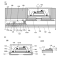
図1(C)に、表示装置100が有する画素130の上面図を示す。1つの画素130には1つのLEDパッケージ150が設けられる。つまり、図1(A)に示す表示部110には、複数のLEDパッケージ150がマトリクス状に設けられている。
Figure 1(C) shows a top view of a
画素130は、導電層131R、導電層131G、導電層131B、導電層132、及びLEDパッケージ150を有する。
図1(D)に、画素130が有するLEDパッケージ150の上面図を示す。
Figure 1(D) shows a top view of the
LEDパッケージ150は、少なくとも1つのLEDチップを有する。本実施の形態では、LEDパッケージ150が、赤色のLEDチップ151R、緑色のLEDチップ151G、及び青色のLEDチップ151Bを有する例を示す。つまり、本実施の形態では、画素130に、R(赤)、G(緑)、B(青)の3色の副画素で1つの色を表現する構成が適用されている。
The
そのほか、画素130には、R、G、B、W(白)の4色の副画素で1つの色を表現する構成、またはR、G、B、Y(黄)の4色の副画素で1つの色を表現する構成等を適用できる。また、色要素に限定はなく、RGBWY以外の色(例えば、シアンまたはマゼンタ等)を用いてもよい。
In addition, the
LEDパッケージ150は、さらに、ヒートシンク154、電極152R、電極152G、電極152B、及び電極153を有する。
The
赤色のLEDチップ151Rは、電極152R上に位置する。緑色のLEDチップ151G及び青色のLEDチップ151Bは、ヒートシンク154上に位置する。
The
赤色のLEDチップ151R、緑色のLEDチップ151G、及び青色のLEDチップ151Bは、それぞれ、ワイヤ143を介して、電極153と電気的に接続されている。
The
赤色のLEDチップ151R、緑色のLEDチップ151G、及び青色のLEDチップ151Bは、互いに異なる色の光を呈する発光ダイオードを有することが好ましい。これにより色変換層を形成する工程が不要となる。したがって、LEDチップの製造コストを抑制することができる。
It is preferable that the
また、赤色のLEDチップ151R、緑色のLEDチップ151G、及び青色のLEDチップ151Bは、同じ色の光を呈する発光ダイオードを有してもよい。このとき、発光ダイオードから発せられた光は、色変換層及び着色層の一方又は双方を介して、表示装置の外部に取り出されてもよい。色変換層及び着色層の一方又は双方は、LEDパッケージ150の内部または上方に設けることができる。
Furthermore, the
また、本実施の形態の表示装置は、赤外光を呈する発光ダイオードを有していてもよい。赤外光を呈する発光ダイオードは、例えば、赤外光センサの光源として用いることができる。 The display device of this embodiment may also have a light-emitting diode that emits infrared light. The light-emitting diode that emits infrared light can be used, for example, as a light source for an infrared light sensor.
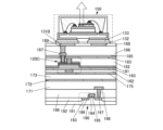
図2(A)に、図1(C)における一点鎖線A-B間の断面図を示す。つまり、図2(A)は、青色のLEDチップ151Bと、当該青色のLEDチップ151Bと電気的に接続される導電層131B及び導電層132と、を含む断面図である。なお、図2(A)では、明瞭化のため、配線など、構成要素の一部を省略する。
Figure 2(A) shows a cross-sectional view taken along dashed line A-B in Figure 1(C). That is, Figure 2(A) is a cross-sectional view including
なお、緑色のLEDチップ151Gと、当該緑色のLEDチップ151Gと電気的に接続される導電層131G及び導電層132とを含む断面構造も、図2(A)と同様であるため、以下の説明を参照できる。
Note that the cross-sectional structure including the
図2(A)に示すように、表示装置100では、トランジスタ120が、導電層131Bを介して、LEDパッケージ150と電気的に接続されている。
As shown in FIG. 2(A), in the
トランジスタ120は、バックゲートとして機能する導電層121、ゲート絶縁層として機能する絶縁層122、半導体層として機能する金属酸化物層123(チャネル形成領域123i及び一対の低抵抗領域123n)、それぞれ低抵抗領域123nと電気的に接続される一対の導電層126a、126b、ゲート絶縁層として機能する絶縁層124、並びに、ゲートとして機能する導電層125を有する。導電層121と金属酸化物層123は、絶縁層122を介して重なる。導電層125と金属酸化物層123は、絶縁層124を介して重なる。
The
トランジスタ120上には、絶縁層127が設けられており、絶縁層127上に導電層131B及び導電層132が設けられている。絶縁層127に設けられた開口を介して、導電層131Bは、導電層126bと電気的に接続されている。
An insulating
絶縁層124及び絶縁層127のうち、少なくとも一層には、水または水素などの不純物が拡散しにくい材料を用いることが好ましい。外部から不純物がトランジスタに拡散することを効果的に抑制することが可能となり、表示装置の信頼性を高めることができる。絶縁層127は、平坦化層としての機能を有する。
At least one of the insulating
図2(A)において、トランジスタ120は、絶縁層104を介して、基板102に設けられている。絶縁層104は、下地膜としての機能を有する。絶縁層104は、基板102から水や水素などの不純物が、トランジスタ120に拡散すること、及び金属酸化物層123から絶縁層104側に酸素が脱離することを防ぐバリア層として機能する。絶縁層104としては、例えば、酸化アルミニウム膜、酸化ハフニウム膜、窒化シリコン膜などの、酸化シリコン膜よりも水素や酸素が拡散しにくい膜を用いることができる。なお、絶縁層104を設けず、基板102上に直接、トランジスタ120を形成してもよい。
In FIG. 2A, the
導電層131Bの端部及び導電層132の端部は、保護層128によって覆われている。保護層128は、導電層131Bの上面に達する開口と、導電層132の上面に達する開口と、を有する。当該開口では、導電層131B及び導電層132が、それぞれ、導電体133を介して、LEDパッケージ150と電気的に接続される。
The ends of
保護層128の材料としては、アクリル、ポリイミド、エポキシ、シリコーンなどの樹脂が好適である。保護層128を設けることで、導電層131B上の導電体133と、導電層132上の導電体133と、が接してショートすることを抑制できる。なお、保護層128は設けなくてもよい。
The material of the
導電体133には、例えば、銀、カーボン、銅などの導電性ペーストや、金、はんだなどのバンプを好適に用いることができる。また、導電体133と接続される導電層131R、131G、131B、132、及び電極152R、152G、152B、153には、それぞれ、導電体133とのコンタクト抵抗の低い導電材料を用いることが好ましい。例えば、導電体133に銀ペーストを用いる場合、これらと接続される導電材料が、アルミニウム、チタン、銅、銀(Ag)とパラジウム(Pd)と銅(Cu)の合金(Ag-Pd-Cu(APC))などであると、コンタクト抵抗が低く好ましい。
For example, conductive paste such as silver, carbon, or copper, or bumps such as gold or solder can be suitably used for the
導電体133は、基板102上に設けてもよく、LEDパッケージ150側に設けてもよい。例えば、導電層131R、131G、131B、132上に、それぞれ、導電体133を設けた後、導電体133とLEDパッケージ150とを接続させることで、基板102上に、LEDパッケージ150を実装することができる。
The
なお、1つのトランジスタに、複数の発光ダイオードが電気的に接続されていてもよい。 In addition, multiple light-emitting diodes may be electrically connected to one transistor.
LEDパッケージ150の側面は、樹脂129で覆われていてもよい。樹脂129として、黒色の樹脂を用いると、表示のコントラストを高められるため、好ましい。また、LEDパッケージ150の上面に、表面保護層、衝撃吸収層などを設けてもよい。LEDパッケージ150は、上側に光を取り出す構成のため、LEDパッケージ150の上面に設ける層は、可視光に対する透過性を有することが好ましい。
The side of the
基板102としては、ガラス基板、石英基板、サファイア基板、セラミック基板等の絶縁性基板、または、シリコンや炭化シリコンなどを材料とした単結晶半導体基板、多結晶半導体基板、シリコンゲルマニウム等の化合物半導体基板、SOI基板などの半導体基板を用いることができる。
The
基板102は、可視光を遮る(可視光に対して非透過性を有する)ことが好ましい。基板102が可視光を遮ることで、基板102に形成されたトランジスタ120に外部から光が入り込むことを抑制することができる。ただし、本発明の一態様はこれに限定されず、基板102は可視光に対する透過性を有していてもよい。
The
また、基板102は、発光ダイオードの光を反射する反射層及び当該光を遮る遮光層の一方及び双方を有していてもよい。
The
LEDパッケージ150が有する複数の発光ダイオード(LEDチップ)は、同じ構成のトランジスタによって駆動されてもよく、それぞれ異なる構成のトランジスタによって駆動されてもよい。例えば、赤色のLEDチップ151Rを駆動するトランジスタと、緑色のLEDチップ151Gを駆動するトランジスタと、青色のLEDチップ151Bを駆動するトランジスタと、は、トランジスタのサイズ、チャネル長、チャネル幅、及び構造などの少なくとも一つが互いに異なっていてもよい。具体的には、所望の輝度で発光させるために必要な電流量に応じて、色ごとにトランジスタのチャネル長及びチャネル幅の一方又は双方を変えてもよい。
The multiple light emitting diodes (LED chips) in the
なお、本実施の形態の表示装置を構成する各種導電層に用いることができる材料としては、アルミニウム、チタン、クロム、ニッケル、銅、イットリウム、ジルコニウム、モリブデン、銀、タンタル、またはタングステンなどの金属、またはこれを主成分とする合金などが挙げられる。またこれらの材料を含む膜を単層で、または積層構造として用いることができる。例えば、シリコンを含むアルミニウム膜の単層構造、チタン膜上にアルミニウム膜を積層する二層構造、タングステン膜上にアルミニウム膜を積層する二層構造、銅-マグネシウム-アルミニウム合金膜上に銅膜を積層する二層構造、チタン膜上に銅膜を積層する二層構造、タングステン膜上に銅膜を積層する二層構造、チタン膜または窒化チタン膜と、その上に重ねてアルミニウム膜または銅膜を積層し、さらにその上にチタン膜または窒化チタン膜を形成する三層構造、モリブデン膜または窒化モリブデン膜と、その上に重ねてアルミニウム膜または銅膜を積層し、さらにその上にモリブデン膜または窒化モリブデン膜を形成する三層構造等がある。なお、酸化インジウム、酸化錫または酸化亜鉛等の酸化物を用いてもよい。また、マンガンを含む銅を用いると、エッチングによる形状の制御性が高まるため好ましい。 Note that materials that can be used for the various conductive layers constituting the display device of this embodiment include metals such as aluminum, titanium, chromium, nickel, copper, yttrium, zirconium, molybdenum, silver, tantalum, and tungsten, or alloys containing these as the main components. In addition, films containing these materials can be used as a single layer or a laminated structure. For example, there are a single layer structure of an aluminum film containing silicon, a two-layer structure in which an aluminum film is laminated on a titanium film, a two-layer structure in which an aluminum film is laminated on a tungsten film, a two-layer structure in which a copper film is laminated on a copper-magnesium-aluminum alloy film, a two-layer structure in which a copper film is laminated on a titanium film, a two-layer structure in which a copper film is laminated on a tungsten film, a three-layer structure in which a titanium film or titanium nitride film is laminated on the titanium film or titanium nitride film, and a three-layer structure in which an aluminum film or copper film is laminated on the titanium film or titanium nitride film, and a three-layer structure in which a molybdenum film or molybdenum nitride film is laminated on the molybdenum film or molybdenum nitride film is laminated on the molybdenum film or molybdenum nitride film. Alternatively, oxides such as indium oxide, tin oxide, or zinc oxide may be used. Also, using copper containing manganese is preferable because it improves the controllability of the shape by etching.
なお、本実施の形態の表示装置を構成する各種絶縁層に用いることができる材料としては、アクリル、ポリイミド、エポキシ、シリコーンなどの樹脂、酸化シリコン、酸化窒化シリコン、窒化酸化シリコン、窒化シリコン、酸化アルミニウムなどの無機絶縁材料が挙げられる。 Note that materials that can be used for the various insulating layers constituting the display device of this embodiment include resins such as acrylic, polyimide, epoxy, and silicone, and inorganic insulating materials such as silicon oxide, silicon oxynitride, silicon nitride oxide, silicon nitride, and aluminum oxide.
図2(B)を用いて、LEDパッケージ150をより詳細に説明する。また、図2(C)を用いて、青色のLEDチップ151Bをより詳細に説明する。
The
図2(B)に示すLEDパッケージ150は、基板141、青色のLEDチップ151B、電極152B、電極153、ヒートシンク154、接着層146、ケース142、ワイヤ143、ワイヤ144、及び封止層145を有する。
The
青色のLEDチップ151Bは、接着層146によって、基板141上に貼り合わされている。青色のLEDチップ151Bは、接着層146を介して、ヒートシンク154と重なるように設けられている。接着層146の材料に特に限定は無いが、後述するように、赤色のLEDチップ151Rは、電極152Rと電気的に接続するように、電極152Rと貼り合わせるため、接着層146が導電性を有すると、各色のLEDチップで接着層146の材料を揃えることができ、好ましい。また、青色のLEDチップ及び緑色のLEDチップにおいて、接着層146として導電性を有する接着剤を用いると、放熱性が高まり好ましい。ヒートシンク154は、電極152B及び電極153と同一の材料及び同一の工程で形成することができる。
The
基板141には、ガラスエポキシ樹脂基板、ポリイミド基板、セラミック基板、アルミナ基板、窒化アルミニウム基板等を用いることができる。
The
図2(C)に示す青色のLEDチップ151Bは、基板101上に発光ダイオード(LED)が設けられた構成を有する。発光ダイオードは、半導体層111、電極112、発光層113、半導体層114、電極115、及び電極116を有する。
The
電極112は、半導体層111と電気的に接続されている。電極116は、電極115を介して半導体層114と電気的に接続されている。電極115及び電極116は一方のみ設けてもよい。発光層113は、半導体層111と半導体層114とに挟持されている。発光層113では、電子と正孔が結合して光を発する。半導体層111と半導体層114とのうち、一方はn型の半導体層であり、他方はp型の半導体層である。
The
青色のLEDチップ151Bにおいて、半導体層111、発光層113、及び半導体層114を含む積層構造は、青色の光を呈するように形成される。
In the
なお、各色の発光ダイオードにおいて、一対の半導体層と、当該一対の半導体層の間の発光層と、を有する積層構造は、赤色、黄色、緑色、または青色などの光を呈するように形成される。当該積層構造には、例えば、ガリウム・リン化合物、ガリウム・ヒ素化合物、ガリウム・アルミニウム・ヒ素化合物、アルミニウム・ガリウム・インジウム・リン化合物、ガリウム窒化物、インジウム・窒化ガリウム化合物、セレン・亜鉛化合物等を用いることができる。 In the light-emitting diodes of each color, a stacked structure having a pair of semiconductor layers and a light-emitting layer between the pair of semiconductor layers is formed to emit light of red, yellow, green, or blue. For example, gallium phosphorus compounds, gallium arsenide compounds, gallium aluminum arsenide compounds, aluminum gallium indium phosphorus compounds, gallium nitride, indium gallium nitride compounds, selenium zinc compounds, etc. can be used for the stacked structure.
基板101としては、例えば、サファイア(Al2O3)基板、炭化シリコン(SiC)基板、シリコン(Si)基板、窒化ガリウム(GaN)基板などの単結晶基板を用いることができる。
As the
電極112は、ワイヤ143を介して、電極152Bと電気的に接続される。電極112は、発光ダイオードの画素電極として機能する。電極116は、ワイヤ144を介して、電極153と電気的に接続される。電極116は、発光ダイオードの共通電極として機能する。
電極152B及び電極153は、それぞれ、ニッケル、銅、銀、白金、または金から選ばれた一元素、または該元素を50%以上含む合金材料で形成することができる。
電極152Bと電極112との接続、及び電極153と電極116との接続には、それぞれ、熱圧着法または超音波ボンディング法を用いたワイヤーボンディング法を用いることができる。
The connection between
ワイヤ143及びワイヤ144には、それぞれ、金、金を含む合金、銅、または銅を含む合金などで形成された金属の細線を用いることができる。
ケース142の材料には、樹脂を用いることができる。ケース142は、少なくとも青色のLEDチップ151Bの側面を覆っていればよく、青色のLEDチップ151Bの上面と重ならなくてもよい。例えば、青色のLEDチップ151Bの上面側では、封止層145が露出していてもよい。ケース142の内側の側面、具体的には、青色のLEDチップ151Bの周囲に、セラミック等からなるリフレクタを設けることが好ましい。青色のLEDチップ151Bが発した光の一部がリフレクタによって反射することで、より多くの光をLEDパッケージ150から取り出すことができる。
The
ケース142の内部は、封止層145で充填されている。封止層145としては、可視光に対する透過性を有する樹脂が好適である。封止層145としては、例えば、エポキシ樹脂、シリコーン樹脂等の紫外線硬化性樹脂、可視光硬化性樹脂などを用いることができる。
The inside of the
図3(A)に、図1(C)における一点鎖線C-D間の断面図を示す。つまり、図3(A)は、赤色のLEDチップ151Rと、当該赤色のLEDチップ151Rと電気的に接続される導電層131R及び導電層132と、を含む断面図である。なお、図3(A)では、明瞭化のため、配線など、構成要素の一部を省略する。
Figure 3(A) shows a cross-sectional view taken along dashed line C-D in Figure 1(C). That is, Figure 3(A) is a cross-sectional view including a
図3(A)に示すように、表示装置100では、トランジスタ120Aが、導電層131Rを介して、LEDパッケージ150と電気的に接続されている。
As shown in FIG. 3(A), in the
トランジスタ120Aは、図2(A)に示すトランジスタ120と同様の構成であるため、詳細な説明は省略する。
トランジスタ120A上には、絶縁層127が設けられており、絶縁層127上に導電層131R及び導電層132が設けられている。絶縁層127に設けられた開口を介して、導電層131Rは、導電層126bと電気的に接続されている。
An insulating
導電層131R及び導電層132は、それぞれ、導電体133を介して、LEDパッケージ150と電気的に接続される。
The
図3(B)を用いて、LEDパッケージ150をより詳細に説明する。また、図3(C)を用いて、赤色のLEDチップ151Rをより詳細に説明する。
The
図3(B)に示すLEDパッケージ150は、基板141、赤色のLEDチップ151R、電極152R、電極153、接着層146、ケース142、ワイヤ144、及び封止層145を有する。
The
赤色のLEDチップ151Rは、導電性を有する接着層146を介して、電極152Rと電気的に接続されている。
The
図3(C)に示す赤色のLEDチップ151Rは、電極103、半導体層117、発光層118、半導体層119、及び電極106を有する。赤色のLEDチップ151Rは、発光ダイオード(LED)ということもできる。また、赤色のLEDチップは、導電性基板上に発光ダイオードが設けられた構成であってもよい。
The
電極103は、半導体層117と電気的に接続されている。電極106は、半導体層119と電気的に接続されている。発光層118は、半導体層117と半導体層119とに挟持されている。発光層118では、電子と正孔が結合して光を発する。半導体層117と半導体層119とのうち、一方はn型の半導体層であり、他方はp型の半導体層である。
The
電極103は、接着層146を介して、電極152Rと電気的に接続される。電極103は、発光ダイオードの画素電極として機能する。電極106は、ワイヤ144を介して、電極153と電気的に接続される。電極106は、発光ダイオードの共通電極として機能する。
図3(D)に示すLEDパッケージ155のように、ケース142の内部には、色変換層147が設けられていてもよい。これにより、発光ダイオードの光は、色変換層147を介して、LEDパッケージ155の外部に射出される。
As shown in FIG. 3D, a
なお、図3(D)では、色変換層147が封止層145の上方に設けられる構成を示すが、色変換層147の配置はこれに限定されない。例えば、色変換層147は、封止層145の内部に分散されていてもよい。
Note that, although FIG. 3D shows a configuration in which the
色変換層147としては、蛍光体や量子ドット(QD:Quantum dot)を用いることが好ましい。特に、量子ドットは、発光スペクトルのピーク幅が狭く、色純度のよい発光を得ることができる。これにより、表示装置の表示品位を高めることができる。
It is preferable to use phosphors or quantum dots (QDs) as the
例えば、LEDパッケージ155に含まれる複数のLEDチップが、いずれも、青色の光を呈する発光ダイオードを有する場合、LEDパッケージ155の内部または上方に色変換層147が設けられていることが好ましい。具体的には、赤色のLEDチップ151Rと重なる位置に、青色の光を赤色に変換する色変換層147が設けられ、緑色のLEDチップ151Gと重なる位置に、青色の光を緑色に変換する色変換層147が設けられていることが好ましい。
For example, if all of the multiple LED chips included in the
これにより、赤色の副画素において、発光ダイオードが発した光は、色変換層147により青色から赤色に変換され、表示装置の外部に射出される。また、緑色の副画素において、発光ダイオードが発した光は、色変換層147により青色から緑色に変換され、表示装置の外部に射出される。また、青色の副画素において、発光ダイオードが発した青色の光が、直接、表示装置の外部に射出される。
As a result, in the red subpixel, the light emitted by the light-emitting diode is converted from blue to red by the
色変換層147は、液滴吐出法(例えば、インクジェット法)、塗布法、インプリント法、各種印刷法(スクリーン印刷、オフセット印刷)等を用いて形成することができる。また、量子ドットフィルムなどの色変換フィルムを用いてもよい。
The
蛍光体としては、蛍光体が表面に印刷または塗装された有機樹脂層、蛍光体が混合された有機樹脂層などを用いることができる。 The phosphor can be an organic resin layer with a phosphor printed or painted on the surface, or an organic resin layer with a phosphor mixed in.
量子ドットを構成する材料としては、特に限定は無く、例えば、第14族元素、第15族元素、第16族元素、複数の第14族元素からなる化合物、第4族から第14族に属する元素と第16族元素との化合物、第2族元素と第16族元素との化合物、第13族元素と第15族元素との化合物、第13族元素と第17族元素との化合物、第14族元素と第15族元素との化合物、第11族元素と第17族元素との化合物、酸化鉄類、酸化チタン類、カルコゲナイドスピネル類、半導体クラスターなどが挙げられる。 The materials constituting the quantum dots are not particularly limited, and examples thereof include Group 14 elements, Group 15 elements, Group 16 elements, compounds consisting of multiple Group 14 elements, compounds of elements belonging to Groups 4 to 14 and Group 16 elements, compounds of Group 2 elements and Group 16 elements, compounds of Group 13 elements and Group 15 elements, compounds of Group 13 elements and Group 17 elements, compounds of Group 14 elements and Group 15 elements, compounds of Group 11 elements and Group 17 elements, iron oxides, titanium oxides, chalcogenide spinels, and semiconductor clusters.
具体的には、セレン化カドミウム、硫化カドミウム、テルル化カドミウム、セレン化亜鉛、酸化亜鉛、硫化亜鉛、テルル化亜鉛、硫化水銀、セレン化水銀、テルル化水銀、砒化インジウム、リン化インジウム、砒化ガリウム、リン化ガリウム、窒化インジウム、窒化ガリウム、アンチモン化インジウム、アンチモン化ガリウム、リン化アルミニウム、砒化アルミニウム、アンチモン化アルミニウム、セレン化鉛、テルル化鉛、硫化鉛、セレン化インジウム、テルル化インジウム、硫化インジウム、セレン化ガリウム、硫化砒素、セレン化砒素、テルル化砒素、硫化アンチモン、セレン化アンチモン、テルル化アンチモン、硫化ビスマス、セレン化ビスマス、テルル化ビスマス、ケイ素、炭化ケイ素、ゲルマニウム、錫、セレン、テルル、ホウ素、炭素、リン、窒化ホウ素、リン化ホウ素、砒化ホウ素、窒化アルミニウム、硫化アルミニウム、硫化バリウム、セレン化バリウム、テルル化バリウム、硫化カルシウム、セレン化カルシウム、テルル化カルシウム、硫化ベリリウム、セレン化ベリリウム、テルル化ベリリウム、硫化マグネシウム、セレン化マグネシウム、硫化ゲルマニウム、セレン化ゲルマニウム、テルル化ゲルマニウム、硫化錫、セレン化錫、テルル化錫、酸化鉛、フッ化銅、塩化銅、臭化銅、ヨウ化銅、酸化銅、セレン化銅、酸化ニッケル、酸化コバルト、硫化コバルト、酸化鉄、硫化鉄、酸化マンガン、硫化モリブデン、酸化バナジウム、酸化タングステン、酸化タンタル、酸化チタン、酸化ジルコニウム、窒化ケイ素、窒化ゲルマニウム、酸化アルミニウム、チタン酸バリウム、セレンと亜鉛とカドミウムの化合物、インジウムと砒素とリンの化合物、カドミウムとセレンと硫黄の化合物、カドミウムとセレンとテルルの化合物、インジウムとガリウムと砒素の化合物、インジウムとガリウムとセレンの化合物、インジウムとセレンと硫黄の化合物、銅とインジウムと硫黄の化合物、及びこれらの組み合わせなどが挙げられる。また、組成が任意の比率で表される、いわゆる合金型量子ドットを用いてもよい。 Specific examples include cadmium selenide, cadmium sulfide, cadmium telluride, zinc selenide, zinc oxide, zinc sulfide, zinc telluride, mercury sulfide, mercury selenide, mercury telluride, indium arsenide, indium phosphide, gallium arsenide, gallium phosphide, indium nitride, gallium nitride, indium antimonide, gallium antimonide, aluminum phosphide, aluminum arsenide, aluminum antimonide, lead selenide, lead telluride, lead sulfide, indium selenide, tere Indium sulfide, Indium sulfide, Gallium selenide, Arsenic sulfide, Arsenic selenide, Arsenic telluride, Antimony sulfide, Antimony selenide, Antimony telluride, Bismuth sulfide, Bismuth selenide, Bismuth telluride, Silicon, Silicon carbide, Germanium, Tin, Selenium, Tellurium, Boron, Carbon, Phosphorus, Boron nitride, Boron phosphide, Boron arsenide, Aluminum nitride, Aluminum sulfide, Barium sulfide, Barium selenide, Barium telluride, Calcium sulfide, Selenide Calcium, calcium telluride, beryllium sulfide, beryllium selenide, beryllium telluride, magnesium sulfide, magnesium selenide, germanium sulfide, germanium selenide, germanium telluride, tin sulfide, tin selenide, tin telluride, lead oxide, copper fluoride, copper chloride, copper bromide, copper iodide, copper oxide, copper selenide, nickel oxide, cobalt oxide, cobalt sulfide, iron oxide, iron sulfide, manganese oxide, molybdenum sulfide, vanadium oxide, tungsten oxide, tungsten oxide Examples of the quantum dots include talc, titanium oxide, zirconium oxide, silicon nitride, germanium nitride, aluminum oxide, barium titanate, compounds of selenium, zinc, and cadmium, compounds of indium, arsenic, and phosphorus, compounds of cadmium, selenium, and sulfur, compounds of cadmium, selenium, and tellurium, compounds of indium, gallium, and arsenic, compounds of indium, gallium, and selenium, compounds of indium, selenium, and sulfur, compounds of copper, indium, and sulfur, and combinations thereof. In addition, so-called alloy-type quantum dots, whose composition is expressed in any ratio, may also be used.
量子ドットの構造としては、コア型、コア-シェル型、コア-マルチシェル型などが挙げられる。また、量子ドットは、表面原子の割合が高いことから、反応性が高く、凝集が起こりやすい。そのため、量子ドットの表面には保護剤が付着している又は保護基が設けられていることが好ましい。当該保護剤が付着している又は保護基が設けられていることによって、凝集を防ぎ、溶媒への溶解性を高めることができる。また、反応性を低減させ、電気的安定性を向上させることも可能である。 Quantum dot structures include core type, core-shell type, and core-multishell type. In addition, quantum dots have a high proportion of surface atoms, so they are highly reactive and prone to aggregation. For this reason, it is preferable that a protective agent is attached to the surface of the quantum dots or that a protective group is provided. By attaching the protective agent or providing the protective group, it is possible to prevent aggregation and increase solubility in a solvent. It is also possible to reduce reactivity and improve electrical stability.
量子ドットは、サイズが小さくなるに従いバンドギャップが大きくなるため、所望の波長の光が得られるように、そのサイズを適宜調整する。結晶のサイズが小さくなるにつれて、量子ドットの発光は青色側へ、つまり、高エネルギー側へシフトするため、量子ドットのサイズを変更させることにより、紫外領域、可視領域、赤外領域のスペクトルの波長領域にわたって、その発光波長を調整することができる。量子ドットのサイズ(直径)は、例えば、0.5nm以上20nm以下、好ましくは1nm以上10nm以下である。量子ドットはそのサイズ分布が狭いほど、発光スペクトルがより狭線化し、色純度の良好な発光を得ることができる。また、量子ドットの形状は特に限定されず、球状、棒状、円盤状、その他の形状であってもよい。棒状の量子ドットである量子ロッドは、指向性を有する光を呈する機能を有する。 Since the band gap of quantum dots increases as the size decreases, the size is adjusted appropriately to obtain light of the desired wavelength. As the size of the crystal decreases, the emission of quantum dots shifts toward the blue side, that is, toward the high energy side, so that the emission wavelength can be adjusted over the wavelength range of the spectrum of the ultraviolet, visible, and infrared regions by changing the size of the quantum dots. The size (diameter) of the quantum dots is, for example, 0.5 nm or more and 20 nm or less, preferably 1 nm or more and 10 nm or less. The narrower the size distribution of the quantum dots, the narrower the emission spectrum becomes, and light with good color purity can be obtained. In addition, the shape of the quantum dots is not particularly limited, and may be spherical, rod-shaped, disk-shaped, or other shapes. Quantum rods, which are rod-shaped quantum dots, have the function of exhibiting directional light.
または、LEDパッケージ155の内部または上方に、色変換層147と着色層の積層構造を有していてもよい。これにより、色変換層147によって変換された光が、着色層を通過することで、光の純度を高められる。また、青色のLEDチップ151Bと重なる位置に、青色の着色層を設けてもよい。青色の着色層を設けると、青色の光の純度を高めることができる。青色の着色層を設けない場合、作製工程を簡略化できる。
Alternatively, a laminated structure of
着色層は特定の波長域の光を透過する有色層である。例えば、赤色、緑色、青色、又は黄色の波長域の光を透過するカラーフィルタなどを用いることができる。着色層に用いることのできる材料としては、金属材料、樹脂材料、顔料又は染料が含まれた樹脂材料などが挙げられる。 The colored layer is a colored layer that transmits light in a specific wavelength range. For example, a color filter that transmits light in the red, green, blue, or yellow wavelength range can be used. Materials that can be used for the colored layer include metal materials, resin materials, and resin materials containing pigments or dyes.
[表示装置の構成例2]
図4~図6に、表示装置の構成例1とは異なる、表示装置の断面構成例をそれぞれ示す。
[Display device configuration example 2]
4 to 6 show examples of cross-sectional configurations of a display device that are different from the first configuration example of the display device.
図4~図6に示す表示装置は、主に、LEDパッケージ150と電気的に接続されるトランジスタの構造が、図2(A)とは異なる。
The display device shown in Figures 4 to 6 differs from that shown in Figure 2 (A) mainly in the structure of the transistor electrically connected to the
図4に示す表示装置では、トランジスタ120Bが、導電層131Bを介して、LEDパッケージ150と電気的に接続されている。
In the display device shown in FIG. 4,
トランジスタ120Bは、ゲートとして機能する導電層121、ゲート絶縁層として機能する絶縁層122、半導体層として機能する金属酸化物層123、ソース及びドレインとして機能する一対の導電層126a、126b、ゲート絶縁層として機能する絶縁層124a、124b、並びに、バックゲートとして機能する導電層125を有する。導電層121と金属酸化物層123は、絶縁層122を介して重なる。導電層125と金属酸化物層123は、絶縁層124a及び絶縁層124bを介して重なる。
The
トランジスタ120B上には、絶縁層127が設けられており、絶縁層127上に導電層131B及び導電層132が設けられている。絶縁層127に設けられた開口を介して、導電層131Bは、導電層126bと電気的に接続されている。
An insulating
図5に示す表示装置では、トランジスタ120Cが、導電層131Bなどを介して、LEDパッケージ150と電気的に接続されている。
In the display device shown in FIG. 5, the
基板174上には、絶縁層175、トランジスタ120C、導電層184a、導電層184b、導電層187、導電層189、絶縁層186、絶縁層188、導電層131B、及び、導電層132等が設けられている。基板174上には、さらに、絶縁層162、絶縁層181、絶縁層182、絶縁層183、及び絶縁層185等の絶縁層が設けられている。これら絶縁層の一つまたは複数は、トランジスタの構成要素とみなされる場合もあるが、本実施の形態では、トランジスタの構成要素に含めずに説明する。
On the
基板151としては、ガラス基板、石英基板、サファイア基板、セラミック基板等の絶縁性基板、または、シリコンや炭化シリコンなどを材料とした単結晶半導体基板、多結晶半導体基板、シリコンゲルマニウム等の化合物半導体基板、SOI基板などの半導体基板を用いることができる。 The substrate 151 may be an insulating substrate such as a glass substrate, a quartz substrate, a sapphire substrate, or a ceramic substrate, or a semiconductor substrate such as a single crystal semiconductor substrate made of silicon or silicon carbide, a polycrystalline semiconductor substrate, a compound semiconductor substrate such as silicon germanium, or an SOI substrate.
基板151は、可視光を遮る(可視光に対して非透過性を有する)ことが好ましい。基板151が可視光を遮ることで、基板151に形成されたトランジスタ120Cに外部から光が入り込むことを抑制することができる。ただし、本発明の一態様はこれに限定されず、基板151は可視光に対する透過性を有していてもよい。
The substrate 151 preferably blocks visible light (is non-transparent to visible light). When the substrate 151 blocks visible light, it is possible to prevent light from entering the
基板174上には、絶縁層175が設けられている。絶縁層175は、基板174から水や水素などの不純物が、トランジスタ120Cに拡散すること、及び金属酸化物層165から絶縁層175側に酸素が脱離することを防ぐバリア層として機能する。絶縁層175としては、例えば、酸化アルミニウム膜、酸化ハフニウム膜、窒化シリコン膜などの、酸化シリコン膜よりも水素や酸素が拡散しにくい膜を用いることができる。
An insulating
トランジスタ120Cは、導電層161、絶縁層163、絶縁層164、金属酸化物層165、一対の導電層166、絶縁層167、導電層168等を有する。
金属酸化物層165は、チャネル形成領域を有する。金属酸化物層165は、一対の導電層166の一方と重なる第1の領域と、一対の導電層166の他方と重なる第2の領域と、当該第1の領域と当該第2の領域の間の第3の領域と、を有する。
The
絶縁層175上に導電層161及び絶縁層162が設けられ、導電層161及び絶縁層162を覆って絶縁層163及び絶縁層164が設けられている。金属酸化物層165は、絶縁層164上に設けられている。導電層161はゲート電極として機能し、絶縁層163及び絶縁層164はゲート絶縁層として機能する。導電層161は絶縁層163及び絶縁層164を介して金属酸化物層165と重なる。絶縁層163は、絶縁層175と同様に、バリア層として機能することが好ましい。金属酸化物層165と接する絶縁層164には、酸化シリコン膜などの酸化物絶縁膜を用いることが好ましい。
The
ここで、導電層161の上面の高さは、絶縁層162の上面の高さと概略一致している。例えば、絶縁層162に開口を設け、当該開口を埋めるように導電層161を形成した後、CMP法などを用いて平坦化処理を施すことで、導電層161の上面の高さと絶縁層162の上面の高さを揃えることができる。これにより、トランジスタ120Cのサイズを小さくすることができる。
Here, the height of the upper surface of the
一対の導電層166は、金属酸化物層165上に離間して設けられている。一対の導電層166は、ソース及びドレインとして機能する。金属酸化物層165及び一対の導電層166を覆って、絶縁層181が設けられ、絶縁層181上に絶縁層182が設けられている。絶縁層181及び絶縁層182には金属酸化物層165に達する開口が設けられており、当該開口の内部に絶縁層167及び導電層168が埋め込まれている。当該開口は、上記第3の領域と重なる。絶縁層167は、絶縁層181の側面及び絶縁層182の側面と重なる。導電層168は、絶縁層167を介して、絶縁層181の側面及び絶縁層182の側面と重なる。導電層168はゲート電極として機能し、絶縁層167はゲート絶縁層として機能する。導電層168は絶縁層167を介して金属酸化物層165と重なる。
The pair of
ここで、導電層168の上面の高さは、絶縁層182の上面の高さと概略一致している。例えば、絶縁層182に開口を設け、当該開口を埋めるように絶縁層167及び導電層168を形成した後、平坦化処理を施すことで、導電層168の上面の高さと絶縁層182の上面の高さを揃えることができる。これにより、トランジスタ120Cのサイズを小さくすることができる。
Here, the height of the upper surface of the
そして、絶縁層182、絶縁層167、及び導電層168の上面を覆って、絶縁層183及び絶縁層185が設けられている。絶縁層181及び絶縁層183は、絶縁層175と同様に、バリア層として機能することが好ましい。絶縁層181で一対の導電層166を覆うことで、絶縁層182に含まれる酸素により一対の導電層166が酸化してしまうことを抑制できる。
The insulating
一対の導電層166の一方及び導電層187と電気的に接続されるプラグが、絶縁層181、絶縁層182、絶縁層183、及び絶縁層185に設けられた開口内に埋め込まれている。プラグは、当該開口の側面及び一対の導電層166の一方の上面に接する導電層184aと、当該導電層184aよりも内側に埋め込まれた導電層184bと、を有することが好ましい。このとき、導電層184aとして、水素及び酸素が拡散しにくい導電材料を用いることが好ましい。
A plug electrically connected to one of the pair of
絶縁層185上に導電層187が設けられ、導電層187上に絶縁層186が設けられている。絶縁層186は、導電層187に達する開口が設けられており、当該開口の内部に導電層189が埋め込まれている。導電層189は導電層187と導電層131Bとを電気的に接続するプラグとして機能する。
A
一対の導電層166の一方は、導電層184a、導電層184b、導電層187、及び導電層189を介して、導電層131Bと電気的に接続されている。
One of the pair of
上述のように、図5に示すトランジスタ120Cでは、導電層161の上面の高さは、絶縁層162の上面の高さと概略一致している。また、図5に示すトランジスタ120Cでは、導電層168の上面の高さが、絶縁層182の上面の高さと概略一致している。
As described above, in the
このように、本実施の形態の表示装置は、ゲート電極の上面の高さが、絶縁層の上面の高さと概略一致しているトランジスタを有することが好ましい。例えば、CMP(Chemical Mechanical Polishing)法などを用いて平坦化処理を施すことで、ゲート電極の上面と絶縁層の上面を平坦化し、ゲート電極の上面の高さと絶縁層の上面の高さを揃えることができる。 In this way, the display device of this embodiment preferably has a transistor in which the height of the upper surface of the gate electrode is approximately the same as the height of the upper surface of the insulating layer. For example, by performing a planarization process using a CMP (Chemical Mechanical Polishing) method or the like, the upper surfaces of the gate electrode and the insulating layer can be planarized, and the height of the upper surface of the gate electrode and the height of the upper surface of the insulating layer can be made uniform.
このような構成のトランジスタは、サイズを小さくすることが容易である。トランジスタのサイズを小さくすることで、画素のサイズを小さくすることができるため、表示装置の精細度を高めることができる。 Transistors with this configuration can be easily reduced in size. By reducing the size of the transistors, the size of the pixels can be reduced, thereby increasing the resolution of the display device.
図6に示す表示装置では、図5に示す表示装置と同様に、トランジスタ120Cが、導電層131Bなどを介して、LEDパッケージ150と電気的に接続されている。
In the display device shown in FIG. 6, similar to the display device shown in FIG. 5, the
図6に示す表示装置は、基板191にチャネル形成領域を有するトランジスタ190と、金属酸化物にチャネル形成領域を有するトランジスタ120Cと、を積層して有する。
The display device shown in FIG. 6 has a
基板191としては、単結晶シリコン基板が好適である。トランジスタ190は、導電層195、絶縁層194、絶縁層196、一対の低抵抗領域193を有する。導電層195は、ゲートとして機能する。絶縁層194は、導電層195と基板191との間に位置し、ゲート絶縁層として機能する。絶縁層196は、導電層195の側面を覆って設けられ、サイドウォールとして機能する。一対の低抵抗領域193は、基板191における、不純物がドープされた領域であり、一方がトランジスタ190のソースとして機能し、他方がトランジスタ190のドレインとして機能する。
A single crystal silicon substrate is suitable as the substrate 191. The
また、基板191に埋め込まれるように、隣接する2つのトランジスタの間に、素子分離層192が設けられている。
In addition, an
トランジスタ190を覆って絶縁層199が設けられ、絶縁層199上に導電層198が設けられている。絶縁層199の開口を介して、導電層198は、一対の低抵抗領域193の一方と電気的に接続される。また、導電層198を覆って絶縁層171が設けられ、絶縁層171上に導電層172が設けられている。導電層198及び導電層172は、それぞれ配線として機能する。また、導電層172を覆って絶縁層173及び絶縁層175が設けられ、絶縁層175上にトランジスタ120Cが設けられている。絶縁層175からLEDパッケージ150までの積層構造は図5に示す表示装置と同様であるため、詳細な説明は省略する。
An insulating
トランジスタ120Cは、画素回路を構成するトランジスタとして用いることができる。また、トランジスタ190は、画素回路を構成するトランジスタや、当該画素回路を駆動するための駆動回路(ゲートドライバ及びソースドライバの一方又は双方)を構成するトランジスタとして用いることができる。また、トランジスタ120C及びトランジスタ190は、それぞれ、演算回路や記憶回路などの各種回路を構成するトランジスタとして用いることができる。
このような構成とすることで、発光ダイオードの直下に画素回路だけでなく駆動回路等を形成することができるため、表示部の外側に駆動回路を設ける場合に比べて、表示装置を小型化することができる。また、狭額縁の(非表示領域の狭い)表示装置を実現することができる。 By configuring in this way, it is possible to form not only pixel circuits but also driving circuits etc. directly under the light-emitting diodes, so the display device can be made smaller than when the driving circuits are provided outside the display section. It is also possible to realize a display device with a narrow frame (narrow non-display area).
本発明の一態様の表示装置は、タッチセンサが搭載された表示装置(入出力装置またはタッチパネルともいう)であってもよい。上述の各表示装置の構成を、タッチパネルに適用することができる。 The display device of one embodiment of the present invention may be a display device equipped with a touch sensor (also referred to as an input/output device or a touch panel). The configuration of each of the display devices described above can be applied to a touch panel.
本発明の一態様のタッチパネルが有する検知素子(センサ素子ともいう)に限定は無い。指やスタイラスなどの被検知体の近接または接触を検知することのできる様々なセンサを、検知素子として適用することができる。 There is no limitation on the detection element (also called a sensor element) of the touch panel of one embodiment of the present invention. Various sensors that can detect the proximity or contact of a detection target such as a finger or a stylus can be used as the detection element.
センサの方式としては、例えば、静電容量方式、抵抗膜方式、表面弾性波方式、赤外線方式、光学方式、感圧方式など様々な方式を用いることができる。 Various sensor types can be used, such as capacitive, resistive, surface acoustic wave, infrared, optical, and pressure-sensitive.
静電容量方式としては、表面型静電容量方式、投影型静電容量方式等がある。また、投影型静電容量方式としては、自己容量方式、相互容量方式等がある。相互容量方式を用いると、同時多点検知が可能となるため好ましい。 The capacitance type includes a surface capacitance type and a projected capacitance type. The projected capacitance type includes a self-capacitance type and a mutual capacitance type. The mutual capacitance type is preferable because it allows simultaneous multi-point detection.
本発明の一態様のタッチパネルは、別々に作製された表示装置と検知素子とを貼り合わせる構成、表示素子を支持する基板及び対向基板の一方または双方に検知素子を構成する電極等を設ける構成等、様々な構成を適用することができる。 The touch panel of one embodiment of the present invention can be configured in various ways, such as by bonding a display device and a sensing element that are separately manufactured, or by providing electrodes that constitute the sensing element on one or both of the substrate supporting the display element and the opposing substrate.
以上のように、本実施の形態の表示装置は、LEDパッケージを、複数のトランジスタが形成された基板に実装することで作製できるため、表示装置の製造の難易度を低くし、歩留まりの向上を図ることができる。また、マイクロLEDと、金属酸化物を用いたトランジスタを組み合わせることで、消費電力の低減された表示装置を実現できる。 As described above, the display device of this embodiment can be manufactured by mounting an LED package on a substrate on which multiple transistors are formed, which makes it easier to manufacture the display device and improves yield. In addition, by combining micro LEDs and transistors using metal oxide, a display device with reduced power consumption can be realized.
また、本実施の形態の表示装置は、トランジスタのサイズを小さくできるため、精細度を高めることや、比較的小さな表示部を有する電子機器への適用が容易である。 In addition, the display device of this embodiment can reduce the size of the transistors, making it easy to increase the resolution and apply it to electronic devices that have relatively small display areas.
本実施の形態は、他の実施の形態と適宜組み合わせることができる。また、本明細書において、1つの実施の形態の中に、複数の構成例が示される場合は、構成例を適宜組み合わせることが可能である。 This embodiment can be combined with other embodiments as appropriate. In addition, in this specification, when multiple configuration examples are shown in one embodiment, the configuration examples can be combined as appropriate.
(実施の形態2)
本実施の形態では、本発明の一態様の表示装置の画素について図7を用いて説明する。
(Embodiment 2)
In this embodiment, a pixel of a display device according to one embodiment of the present invention will be described with reference to FIGS.
[画素]
本実施の形態の表示装置は、m行n列(m、nは、それぞれ1以上の整数)のマトリクス状に配置された複数の画素を有する。図7に、画素200(i,j)(iは1以上m以下の整数、jは1以上n以下の整数)の回路図の一例を示す。
[Pixels]
The display device of this embodiment has a plurality of pixels arranged in a matrix of m rows and n columns (m and n are each an integer equal to or greater than 1). Fig. 7 shows an example of a circuit diagram of a pixel 200(i,j) (i is an integer equal to or greater than 1 and equal to or less than m, and j is an integer equal to or greater than 1 and equal to or less than n).
図7に示す画素200(i,j)は、発光素子210、スイッチSW21、スイッチSW22、トランジスタM、及び容量素子C1を有する。
The pixel 200(i,j) shown in FIG. 7 has a light-emitting
本実施の形態では、スイッチSW21として、トランジスタを用いる例を示す。スイッチSW21のゲートは、走査線GL1(i)と電気的に接続される。スイッチSW21のソース及びドレインは、一方が信号線SL(j)と電気的に接続され、他方がトランジスタMのゲートと電気的に接続される。 In this embodiment, an example is shown in which a transistor is used as the switch SW21. The gate of the switch SW21 is electrically connected to the scanning line GL1(i). One of the source and drain of the switch SW21 is electrically connected to the signal line SL(j), and the other is electrically connected to the gate of the transistor M.
本実施の形態では、スイッチSW22として、トランジスタを用いる例を示す。スイッチSW22のゲートは、走査線GL2(i)と電気的に接続される。スイッチSW22のソース及びドレインは、一方が配線COMと電気的に接続され、他方がトランジスタMのゲートと電気的に接続される。 In this embodiment, an example in which a transistor is used as the switch SW22 is shown. The gate of the switch SW22 is electrically connected to the scan line GL2(i). One of the source and drain of the switch SW22 is electrically connected to the wiring COM, and the other is electrically connected to the gate of the transistor M.
トランジスタMのゲートは、容量素子C1の一方の電極、スイッチSW21のソース及びドレインの他方、及びスイッチSW22のソース及びドレインの他方と電気的に接続される。トランジスタMのソース及びドレインは、一方が配線CATHODEと電気的に接続され、他方が発光素子210のカソードと電気的に接続される。
The gate of the transistor M is electrically connected to one electrode of the capacitance element C1, the other of the source and drain of the switch SW21, and the other of the source and drain of the switch SW22. One of the source and drain of the transistor M is electrically connected to the wiring CATHODE, and the other is electrically connected to the cathode of the light-emitting
容量素子C1の他方の電極は、配線CATHODEと電気的に接続される。 The other electrode of the capacitance element C1 is electrically connected to the wiring CATHODE.
発光素子210のアノードは、配線ANODEと電気的に接続される。
The anode of the light-emitting
走査線GL1(i)は、選択信号を供給する機能を有する。走査線GL2(i)は、制御信号を供給する機能を有する。信号線SL(j)は、画像信号を供給する機能を有する。配線VCOM、配線CATHODE、及び配線ANODEには、それぞれ定電位が供給される。発光素子210のアノード側を高電位に、カソード側をアノード側よりも低電位にすることができる。
The scanning line GL1(i) has a function of supplying a selection signal. The scanning line GL2(i) has a function of supplying a control signal. The signal line SL(j) has a function of supplying an image signal. A constant potential is supplied to the wiring VCOM, the wiring CATHODE, and the wiring ANODE. The anode side of the light-emitting
スイッチSW21は、選択信号により制御され、画素200の選択状態を制御するための選択トランジスタとして機能する。
Switch SW21 is controlled by a selection signal and functions as a selection transistor to control the selection state of
トランジスタMは、ゲートに供給される電位に応じて発光素子210に流れる電流を制御する駆動トランジスタとして機能する。スイッチSW21が導通状態のとき、信号線SL(j)に供給される画像信号がトランジスタMのゲートに供給され、その電位に応じて、発光素子210の発光輝度を制御することができる。
Transistor M functions as a drive transistor that controls the current flowing through light-emitting
スイッチSW22は、制御信号に基づいてトランジスタMのゲート電位を制御する機能を有する。具体的には、スイッチSW22は、トランジスタMを非導通状態にする電位を、トランジスタMのゲートに供給することができる。 Switch SW22 has a function of controlling the gate potential of transistor M based on a control signal. Specifically, switch SW22 can supply a potential to the gate of transistor M that puts transistor M into a non-conductive state.
スイッチSW22は、例えば、パルス幅の制御に用いることができる。制御信号に基づく期間、トランジスタMから発光素子210に電流を供給することができる。または、発光素子210は、画像信号及び制御信号に基づいて、階調を表現することができる。
The switch SW22 can be used, for example, to control the pulse width. A current can be supplied from the transistor M to the light-emitting
ここで、画素200(i,j)が有するトランジスタには、それぞれチャネルが形成される半導体層に金属酸化物(酸化物半導体)を用いたトランジスタを適用することが好ましい。 Here, it is preferable that the transistors in pixel 200(i,j) are transistors that use metal oxide (oxide semiconductor) in the semiconductor layer in which the channel is formed.
シリコンよりもバンドギャップが広く、かつキャリア密度の小さい金属酸化物を用いたトランジスタは、極めて小さいオフ電流を実現することができる。そのため、その小さいオフ電流により、トランジスタと直列に接続された容量素子に蓄積した電荷を長期間に亘って保持することが可能である。そのため、特に容量素子C1に直列に接続されるスイッチSW21及びスイッチSW22には、酸化物半導体が適用されたトランジスタを用いることが好ましい。また、これ以外のトランジスタも同様に酸化物半導体を適用したトランジスタを用いることで、作製コストを低減することができる。 Transistors using metal oxides, which have a wider band gap than silicon and a lower carrier density, can achieve an extremely small off-current. Therefore, due to the small off-current, it is possible to hold the charge accumulated in the capacitor connected in series with the transistor for a long period of time. Therefore, it is preferable to use transistors using oxide semiconductors, particularly for the switches SW21 and SW22 connected in series with the capacitor C1. In addition, by using transistors using oxide semiconductors for other transistors as well, the manufacturing cost can be reduced.
また、画素200(i,j)が有するトランジスタに、チャネルが形成される半導体にシリコンを適用したトランジスタを用いることもできる。特に単結晶シリコンや多結晶シリコンなどの結晶性の高いシリコンを用いることで、高い電界効果移動度を実現することができ、より高速な動作が可能となるため好ましい。 In addition, the transistor in pixel 200(i,j) may be a transistor in which silicon is used as the semiconductor in which the channel is formed. In particular, the use of silicon with high crystallinity, such as single crystal silicon or polycrystalline silicon, is preferable because it can achieve high field effect mobility and enable faster operation.
また、画素200(i,j)が有するトランジスタのうち、一以上に酸化物半導体を適用したトランジスタを用い、それ以外にシリコンを適用したトランジスタを用いる構成としてもよい。 In addition, one or more of the transistors included in pixel 200(i,j) may be a transistor that uses an oxide semiconductor, and the rest may be transistors that use silicon.
なお、図7において、トランジスタをnチャネル型のトランジスタとして表記しているが、pチャネル型のトランジスタを用いることもできる。 Note that in Figure 7, the transistors are shown as n-channel transistors, but p-channel transistors can also be used.
[トランジスタ]
次に、表示装置に用いることができるトランジスタについて、説明する。
[Transistor]
Next, a transistor that can be used in a display device will be described.
表示装置が有するトランジスタの構造は特に限定されない。例えば、プレーナ型のトランジスタとしてもよいし、スタガ型のトランジスタとしてもよいし、逆スタガ型のトランジスタとしてもよい。また、トップゲート構造またはボトムゲート構造のいずれのトランジスタ構造としてもよい。または、チャネルの上下にゲート電極が設けられていてもよい。 The structure of the transistors in the display device is not particularly limited. For example, the transistors may be planar type, staggered type, or inverted staggered type. In addition, the transistor may have either a top-gate structure or a bottom-gate structure. Alternatively, gate electrodes may be provided above and below the channel.
表示装置が有するトランジスタには、例えば、金属酸化物をチャネル形成領域に用いたトランジスタを用いることができる。これにより、オフ電流の極めて小さいトランジスタを実現することができる。 For example, a transistor that uses metal oxide in a channel formation region can be used as the transistor in the display device. This makes it possible to realize a transistor with an extremely small off-state current.
または、表示装置が有するトランジスタにシリコンをチャネル形成領域に有するトランジスタを適用してもよい。当該トランジスタとしては、例えば、アモルファスシリコンを有するトランジスタ、結晶性のシリコン(代表的には、低温ポリシリコン)を有するトランジスタ、単結晶シリコンを有するトランジスタなどが挙げられる。 Alternatively, a transistor having silicon in a channel formation region may be applied to the transistor of the display device. Examples of such a transistor include a transistor having amorphous silicon, a transistor having crystalline silicon (typically, low-temperature polysilicon), and a transistor having single crystal silicon.
[金属酸化物]
以下では、半導体層に適用可能な金属酸化物について説明する。
[Metal oxide]
Metal oxides that can be used for the semiconductor layer will be described below.
金属酸化物は、少なくともインジウムまたは亜鉛を含むことが好ましい。特に、インジウム及び亜鉛を含むことが好ましい。また、それらに加えて、アルミニウム、ガリウム、イットリウムまたは錫などが含まれていることが好ましい。また、ホウ素、チタン、鉄、ニッケル、ゲルマニウム、ジルコニウム、モリブデン、ランタン、セリウム、ネオジム、ハフニウム、タンタル、タングステン、またはマグネシウムなどから選ばれた一種、または複数種が含まれていてもよい。 The metal oxide preferably contains at least indium or zinc. In particular, it is preferable that it contains indium and zinc. In addition to these, it is preferable that it contains aluminum, gallium, yttrium, tin, or the like. It may also contain one or more elements selected from boron, titanium, iron, nickel, germanium, zirconium, molybdenum, lanthanum, cerium, neodymium, hafnium, tantalum, tungsten, magnesium, and the like.
ここでは、金属酸化物が、インジウム、元素M、及び亜鉛を有するIn-M-Zn酸化物である場合を考える。なお、元素Mは、アルミニウム、ガリウム、イットリウム、または錫などとする。そのほか、元素Mに適用可能な元素としては、ホウ素、チタン、鉄、ニッケル、ゲルマニウム、ジルコニウム、モリブデン、ランタン、セリウム、ネオジム、ハフニウム、タンタル、タングステン、マグネシウムなどがある。ただし、元素Mとして、前述の元素を複数組み合わせても構わない場合がある。 Here, we consider the case where the metal oxide is an In-M-Zn oxide having indium, element M, and zinc. The element M is aluminum, gallium, yttrium, tin, or the like. Other elements that can be used for element M include boron, titanium, iron, nickel, germanium, zirconium, molybdenum, lanthanum, cerium, neodymium, hafnium, tantalum, tungsten, magnesium, and the like. However, there are cases where a combination of multiple of the above elements may be used as element M.
金属酸化物膜は、スパッタリング法により形成することができる。そのほか、PLD法、PECVD法、熱CVD法、ALD法、真空蒸着法などを用いてもよい。 The metal oxide film can be formed by sputtering. Other methods that can be used include PLD, PECVD, thermal CVD, ALD, and vacuum deposition.
なお、本明細書等において、窒素を有する金属酸化物も金属酸化物(metal oxide)と総称する場合がある。また、窒素を有する金属酸化物を、金属酸窒化物(metal oxynitride)と呼称してもよい。例えば、亜鉛酸窒化物(ZnON)などの窒素を有する金属酸化物を、半導体層に用いてもよい。 In this specification and the like, metal oxides containing nitrogen may also be collectively referred to as metal oxides. Metal oxides containing nitrogen may also be referred to as metal oxynitrides. For example, metal oxides containing nitrogen, such as zinc oxynitride (ZnON), may be used in the semiconductor layer.
なお、本明細書等において、CAAC(c-axis aligned crystal)、及びCAC(Cloud-Aligned Composite)と記載する場合がある。CAACは結晶構造の一例を表し、CACは機能または材料の構成の一例を表す。 Note that in this specification and elsewhere, the terms CAAC (c-axis aligned crystal) and CAC (Cloud-Aligned Composite) may be used. CAAC represents an example of a crystal structure, and CAC represents an example of a function or material configuration.
例えば、半導体層にはCAC(Cloud-Aligned Composite)-OSを用いることができる。 For example, CAC (Cloud-Aligned Composite)-OS can be used for the semiconductor layer.
CAC-OSまたはCAC-metal oxideとは、材料の一部では導電性の機能と、材料の一部では絶縁性の機能とを有し、材料の全体では半導体としての機能を有する。なお、CAC-OSまたはCAC-metal oxideを、トランジスタの半導体層に用いる場合、導電性の機能は、キャリアとなる電子(またはホール)を流す機能であり、絶縁性の機能は、キャリアとなる電子を流さない機能である。導電性の機能と、絶縁性の機能とを、それぞれ相補的に作用させることで、スイッチングさせる機能(On/Offさせる機能)をCAC-OSまたはCAC-metal oxideに付与することができる。CAC-OSまたはCAC-metal oxideにおいて、それぞれの機能を分離させることで、双方の機能を最大限に高めることができる。 CAC-OS or CAC-metal oxide has a conductive function in part of the material and an insulating function in part of the material, and functions as a semiconductor in its entirety. When CAC-OS or CAC-metal oxide is used in the semiconductor layer of a transistor, the conductive function is a function of flowing electrons (or holes) that become carriers, and the insulating function is a function of not flowing electrons that become carriers. By making the conductive function and the insulating function act in a complementary manner, it is possible to impart a switching function (on/off function) to CAC-OS or CAC-metal oxide. By separating the respective functions in CAC-OS or CAC-metal oxide, it is possible to maximize both functions.
また、CAC-OSまたはCAC-metal oxideは、導電性領域、及び絶縁性領域を有する。導電性領域は、上述の導電性の機能を有し、絶縁性領域は、上述の絶縁性の機能を有する。また、材料中において、導電性領域と、絶縁性領域とは、ナノ粒子レベルで分離している場合がある。また、導電性領域と、絶縁性領域とは、それぞれ材料中に偏在する場合がある。また、導電性領域は、周辺がぼけてクラウド状に連結して観察される場合がある。 CAC-OS or CAC-metal oxide has conductive regions and insulating regions. The conductive regions have the conductive function described above, and the insulating regions have the insulating function described above. In addition, the conductive regions and the insulating regions may be separated at the nanoparticle level in the material. The conductive regions and the insulating regions may be unevenly distributed in the material. In addition, the conductive regions may be observed connected in a cloud shape with the periphery blurred.
また、CAC-OSまたはCAC-metal oxideにおいて、導電性領域と、絶縁性領域とは、それぞれ0.5nm以上10nm以下、好ましくは0.5nm以上3nm以下のサイズで材料中に分散している場合がある。 In addition, in CAC-OS or CAC-metal oxide, the conductive regions and the insulating regions may each be dispersed in the material with a size of 0.5 nm to 10 nm, preferably 0.5 nm to 3 nm.
また、CAC-OSまたはCAC-metal oxideは、異なるバンドギャップを有する成分により構成される。例えば、CAC-OSまたはCAC-metal oxideは、絶縁性領域に起因するワイドギャップを有する成分と、導電性領域に起因するナローギャップを有する成分と、により構成される。当該構成の場合、キャリアを流す際に、ナローギャップを有する成分において、主にキャリアが流れる。また、ナローギャップを有する成分が、ワイドギャップを有する成分に相補的に作用し、ナローギャップを有する成分に連動してワイドギャップを有する成分にもキャリアが流れる。このため、上記CAC-OSまたはCAC-metal oxideをトランジスタのチャネル形成領域に用いる場合、トランジスタのオン状態において高い電流駆動力、つまり大きなオン電流、及び高い電界効果移動度を得ることができる。 In addition, CAC-OS or CAC-metal oxide is composed of components having different band gaps. For example, CAC-OS or CAC-metal oxide is composed of a component having a wide gap due to an insulating region and a component having a narrow gap due to a conductive region. In this configuration, when carriers are caused to flow, the carriers mainly flow in the component having the narrow gap. In addition, the component having the narrow gap acts complementarily to the component having the wide gap, and carriers also flow in the component having the wide gap in conjunction with the component having the narrow gap. Therefore, when the above CAC-OS or CAC-metal oxide is used in the channel formation region of a transistor, a high current driving force in the on state of the transistor, that is, a large on-current and high field effect mobility can be obtained.
すなわち、CAC-OSまたはCAC-metal oxideは、マトリックス複合材(matrix composite)、または金属マトリックス複合材(metal matrix composite)と呼称することもできる。 In other words, CAC-OS or CAC-metal oxide can also be called a matrix composite or a metal matrix composite.
酸化物半導体(金属酸化物)は、単結晶酸化物半導体と、それ以外の非単結晶酸化物半導体と、に分けられる。非単結晶酸化物半導体としては、例えば、CAAC-OS(c-axis aligned crystalline oxide semiconductor)、多結晶酸化物半導体、nc-OS(nanocrystalline oxide semiconductor)、擬似非晶質酸化物半導体(a-like OS:amorphous-like oxide semiconductor)、及び非晶質酸化物半導体などがある。 Oxide semiconductors (metal oxides) are divided into single-crystal oxide semiconductors and other non-single-crystal oxide semiconductors. Examples of non-single-crystal oxide semiconductors include CAAC-OS (c-axis aligned crystalline oxide semiconductor), polycrystalline oxide semiconductors, nc-OS (nanocrystalline oxide semiconductor), pseudo-amorphous oxide semiconductors (a-like OS: amorphous-like oxide semiconductor), and amorphous oxide semiconductors.
CAAC-OSは、c軸配向性を有し、かつa-b面方向において複数のナノ結晶が連結し、歪みを有した結晶構造となっている。なお、歪みとは、複数のナノ結晶が連結する領域において、格子配列の揃った領域と、別の格子配列の揃った領域と、の間で格子配列の向きが変化している箇所を指す。 CAAC-OS has a c-axis orientation and has a crystal structure in which multiple nanocrystals are connected in the a-b plane direction and have distortion. Note that distortion refers to a location in a region where multiple nanocrystals are connected, where the direction of the lattice arrangement changes between a region with a uniform lattice arrangement and a region with a different uniform lattice arrangement.
ナノ結晶は、六角形を基本とするが、正六角形状とは限らず、非正六角形状である場合がある。また、歪みにおいて、五角形及び七角形などの格子配列を有する場合がある。なお、CAAC-OSにおいて、歪み近傍においても、明確な結晶粒界(グレインバウンダリーともいう。)を確認することは難しい。すなわち、格子配列の歪みによって、結晶粒界の形成が抑制されていることがわかる。これは、CAAC-OSが、a-b面方向において酸素原子の配列が稠密でないことや、金属元素が置換することで原子間の結合距離が変化することなどによって、歪みを許容することができるためである。 Nanocrystals are basically hexagonal, but are not limited to regular hexagonal shapes and may be non-regular hexagonal. The distortion may have a lattice arrangement such as a pentagon or heptagon. It is difficult to confirm clear crystal grain boundaries (also called grain boundaries) in the vicinity of the distortion in CAAC-OS. In other words, it is found that the formation of crystal grain boundaries is suppressed by the distortion of the lattice arrangement. This is because CAAC-OS can tolerate distortion due to the fact that the arrangement of oxygen atoms in the a-b plane direction is not dense and the bond distance between atoms changes due to substitution of metal elements.
また、CAAC-OSは、インジウム、及び酸素を有する層(以下、In層)と、元素M、亜鉛、及び酸素を有する層(以下、(M,Zn)層)とが積層した、層状の結晶構造(層状構造ともいう)を有する傾向がある。なお、インジウムと元素Mは、互いに置換可能であり、(M,Zn)層の元素Mがインジウムと置換した場合、(In,M,Zn)層と表すこともできる。また、In層のインジウムが元素Mと置換した場合、(In,M)層と表すこともできる。 In addition, CAAC-OS tends to have a layered crystal structure (also referred to as a layered structure) in which a layer containing indium and oxygen (hereinafter, an In layer) and a layer containing the element M, zinc, and oxygen (hereinafter, an (M, Zn) layer) are stacked. Note that indium and the element M can be substituted for each other, and when the element M in the (M, Zn) layer is substituted for indium, it can also be represented as an (In, M, Zn) layer. When the indium in the In layer is substituted for the element M, it can also be represented as an (In, M) layer.
CAAC-OSは結晶性の高い金属酸化物である。一方、CAAC-OSは、明確な結晶粒界を確認することが難しいため、結晶粒界に起因する電子移動度の低下が起こりにくいといえる。また、金属酸化物の結晶性は不純物の混入や欠陥の生成などによって低下する場合があるため、CAAC-OSは不純物や欠陥(酸素欠損(VO:oxygen vacancyともいう。)など)の少ない金属酸化物ともいえる。したがって、CAAC-OSを有する金属酸化物は、物理的性質が安定する。そのため、CAAC-OSを有する金属酸化物は熱に強く、信頼性が高い。 CAAC-OS is a metal oxide with high crystallinity. On the other hand, since it is difficult to confirm clear crystal boundaries in CAAC-OS, it can be said that a decrease in electron mobility due to crystal boundaries is unlikely to occur. In addition, since the crystallinity of a metal oxide can be decreased by the inclusion of impurities or the generation of defects, CAAC-OS can be said to be a metal oxide with few impurities or defects (oxygen vacancies (V 2 O 3 , also referred to as oxygen vacancies)). Therefore, metal oxides having CAAC-OS have stable physical properties. Therefore, metal oxides having CAAC-OS are resistant to heat and highly reliable.
nc-OSは、微小な領域(例えば、1nm以上10nm以下の領域、特に1nm以上3nm以下の領域)において原子配列に周期性を有する。また、nc-OSは、異なるナノ結晶間で結晶方位に規則性が見られない。そのため、膜全体で配向性が見られない。したがって、nc-OSは、分析方法によっては、a-like OSや非晶質酸化物半導体と区別が付かない場合がある。 NC-OS has periodic atomic arrangement in a small region (for example, a region of 1 nm to 10 nm, particularly a region of 1 nm to 3 nm). In addition, NC-OS does not show regularity in the crystal orientation between different nanocrystals. Therefore, no orientation is seen throughout the film. Therefore, NC-OS may be indistinguishable from a-like OS or amorphous oxide semiconductor depending on the analysis method.
なお、インジウムと、ガリウムと、亜鉛と、を有する金属酸化物の一種である、インジウム-ガリウム-亜鉛酸化物(以下、IGZO)は、上述のナノ結晶とすることで安定な構造をとる場合がある。特に、IGZOは、大気中では結晶成長がし難い傾向があるため、大きな結晶(ここでは、数mmの結晶、または数cmの結晶)よりも小さな結晶(例えば、上述のナノ結晶)とする方が、構造的に安定となる場合がある。 Note that indium gallium zinc oxide (hereinafter referred to as IGZO), a type of metal oxide containing indium, gallium, and zinc, may have a stable structure when made into the above-mentioned nanocrystals. In particular, since IGZO tends to have difficulty in crystal growth in the atmosphere, it may be structurally more stable when made into small crystals (for example, the above-mentioned nanocrystals) rather than large crystals (here, crystals of several mm or several cm).
a-like OSは、nc-OSと非晶質酸化物半導体との間の構造を有する金属酸化物である。a-like OSは、鬆または低密度領域を有する。すなわち、a-like OSは、nc-OS及びCAAC-OSと比べて、結晶性が低い。 A-like OS is a metal oxide having a structure between nc-OS and an amorphous oxide semiconductor. A-like OS has voids or low-density regions. That is, a-like OS has lower crystallinity than nc-OS and CAAC-OS.
酸化物半導体(金属酸化物)は、多様な構造をとり、それぞれが異なる特性を有する。本発明の一態様の酸化物半導体は、非晶質酸化物半導体、多結晶酸化物半導体、a-like OS、nc-OS、CAAC-OSのうち、二種以上を有していてもよい。 Oxide semiconductors (metal oxides) have a variety of structures, each of which has different characteristics. The oxide semiconductor of one embodiment of the present invention may have two or more of an amorphous oxide semiconductor, a polycrystalline oxide semiconductor, an a-like OS, an nc-OS, and a CAAC-OS.
半導体層として機能する金属酸化物膜は、不活性ガス及び酸素ガスのいずれか一方または双方を用いて成膜することができる。なお、金属酸化物膜の成膜時における酸素の流量比(酸素分圧)に、特に限定はない。ただし、電界効果移動度が高いトランジスタを得る場合においては、金属酸化物膜の成膜時における酸素の流量比(酸素分圧)は、0%以上30%以下が好ましく、5%以上30%以下がより好ましく、7%以上15%以下がさらに好ましい。 The metal oxide film that functions as the semiconductor layer can be formed using either or both of an inert gas and oxygen gas. There is no particular limitation on the flow rate ratio of oxygen (oxygen partial pressure) during the formation of the metal oxide film. However, in order to obtain a transistor with high field effect mobility, the flow rate ratio of oxygen (oxygen partial pressure) during the formation of the metal oxide film is preferably 0% or more and 30% or less, more preferably 5% or more and 30% or less, and even more preferably 7% or more and 15% or less.
金属酸化物は、エネルギーギャップが2eV以上であることが好ましく、2.5eV以上であることがより好ましく、3eV以上であることがさらに好ましい。このように、エネルギーギャップの広い金属酸化物を用いることで、トランジスタのオフ電流を低減することができる。 The metal oxide preferably has an energy gap of 2 eV or more, more preferably 2.5 eV or more, and even more preferably 3 eV or more. In this way, by using a metal oxide with a wide energy gap, the off-current of the transistor can be reduced.
本実施の形態は、他の実施の形態と適宜組み合わせることができる。 This embodiment can be combined with other embodiments as appropriate.
(実施の形態3)
本実施の形態では、本発明の一態様の電子機器について、図8~図12を用いて説明する。
(Embodiment 3)
In this embodiment, electronic devices according to one embodiment of the present invention will be described with reference to FIGS.
本実施の形態の電子機器は、表示部に本発明の一態様の表示装置を有する。本発明の一態様の表示装置は、表示品位が高く、かつ、消費電力が低い。また、本発明の一態様の表示装置は、高精細化及び大型化が容易である。したがって、様々な電子機器の表示部に用いることができる。 The electronic device of this embodiment has a display device of one embodiment of the present invention in a display portion. The display device of one embodiment of the present invention has high display quality and low power consumption. In addition, the display device of one embodiment of the present invention can be easily made large and highly precise. Therefore, the display device can be used in the display portion of various electronic devices.
電子機器としては、例えば、テレビジョン装置、デスクトップ型もしくはノート型のパーソナルコンピュータ、コンピュータ用などのモニタ、デジタルサイネージ、パチンコ機などの大型ゲーム機などの比較的大きな画面を備える電子機器の他、デジタルカメラ、デジタルビデオカメラ、デジタルフォトフレーム、携帯電話機、携帯型ゲーム機、携帯情報端末、音響再生装置、などが挙げられる。 Examples of electronic devices include electronic devices with relatively large screens such as television sets, desktop or notebook personal computers, computer monitors, digital signage, large game machines such as pachinko machines, as well as digital cameras, digital video cameras, digital photo frames, mobile phones, portable game machines, personal digital assistants, and audio playback devices.
特に、本発明の一態様の表示装置は、精細度を高めることが可能なため、比較的小さな表示部を有する電子機器に好適に用いることができる。このような電子機器としては、例えば腕時計型やブレスレット型の情報端末機(ウェアラブル機器)や、ヘッドマウントディスプレイなどのVR(Virtual Reality)向け機器、メガネ型のAR(Augmented Reality)向け機器、またはMR(Mixed Reality)向け機器等、頭部に装着可能なウェアラブル機器等に好適に用いることができる。 In particular, the display device of one embodiment of the present invention can be suitably used in electronic devices having a relatively small display area because it can increase the resolution. Examples of such electronic devices include wristwatch-type or bracelet-type information terminals (wearable devices), VR (Virtual Reality) devices such as head-mounted displays, glasses-type AR (Augmented Reality) devices, and MR (Mixed Reality) devices that can be worn on the head, and other wearable devices.
本実施の形態の電子機器は、センサ(力、変位、位置、速度、加速度、角速度、回転数、距離、光、液、磁気、温度、化学物質、音声、時間、硬度、電場、電流、電圧、電力、放射線、流量、湿度、傾度、振動、においまたは赤外線を測定する機能を含むもの)を有していてもよい。 The electronic device of this embodiment may have a sensor (including a function to measure force, displacement, position, velocity, acceleration, angular velocity, rotation speed, distance, light, liquid, magnetism, temperature, chemicals, sound, time, hardness, electric field, current, voltage, power, radiation, flow rate, humidity, gradient, vibration, odor, or infrared light).
本実施の形態の電子機器は、様々な機能を有することができる。例えば、様々な情報(静止画、動画、テキスト画像など)を表示部に表示する機能、タッチパネル機能、カレンダー、日付または時刻などを表示する機能、様々なソフトウェア(プログラム)を実行する機能、無線通信機能、記録媒体に記録されているプログラムまたはデータを読み出す機能等を有することができる。 The electronic device of this embodiment can have various functions. For example, it can have a function to display various information (still images, videos, text images, etc.) on the display unit, a touch panel function, a function to display a calendar, date or time, etc., a function to execute various software (programs), a wireless communication function, a function to read out programs or data recorded on a recording medium, etc.
図8(A)に、メガネ型の電子機器900の斜視図を示す。電子機器900は、一対の表示パネル901、一対の筐体902、一対の光学部材903、一対の装着部904等を有する。
Figure 8 (A) shows a perspective view of a glasses-type
電子機器900は、光学部材903の表示領域906に、表示パネル901で表示した画像を投影することができる。光学部材903は透光性を有するため、ユーザーは光学部材903を通して視認される透過像に重ねて、表示領域906に表示された画像を見ることができる。したがって、電子機器900は、AR表示が可能な電子機器である。
The
電子機器900が備える表示パネル901は、画像を表示する機能に加えて、撮像する機能を有することが好ましい。このとき、電子機器900は、光学部材903を介して表示パネル901に入射された光を受光し、電気信号に変換して出力することができる。これにより、ユーザーの目、または目及びその周辺を撮像し、画像情報として外部、または電子機器900が備える演算部に出力することができる。
The
一つの筐体902には、前方を撮像することのできるカメラ905が設けられている。また図示しないが、いずれか一方の筐体902には無線受信機、またはケーブルを接続可能なコネクタが設けられ、筐体902に映像信号等を供給することができる。また、筐体902に、ジャイロセンサなどの加速度センサを配置することで、ユーザーの頭部の向きを検知して、その向きに応じた画像を表示領域906に表示することもできる。また、筐体902にはバッテリが設けられていることが好ましく、無線または有線によって充電することができることが好ましい。
One of the
図8(B)を用いて、電子機器900の表示領域906への画像の投影方法について説明する。筐体902の内部には、表示パネル901、レンズ911、反射板912が設けられている。また、光学部材903の表示領域906に相当する部分には、ハーフミラーとして機能する反射面913を有する。
A method of projecting an image onto the
表示パネル901から発せられた光915は、レンズ911を通過し、反射板912により光学部材903側へ反射される。光学部材903の内部において、光915は光学部材903の端面で全反射を繰り返し、反射面913に到達することで、反射面913に画像が投影される。これにより、ユーザーは、反射面913に反射された光915と、光学部材903(反射面913を含む)を透過した透過光916の両方を視認することができる。
図8では、反射板912及び反射面913がそれぞれ曲面を有する例を示している。これにより、これらが平面である場合に比べて、光学設計の自由度を高めることができ、光学部材903の厚さを薄くすることができる。なお、反射板912及び反射面913を平面としてもよい。
FIG. 8 shows an example in which the
反射板912としては、鏡面を有する部材を用いることができ、反射率が高いことが好ましい。また、反射面913としては、金属膜の反射を利用したハーフミラーを用いてもよいが、全反射を利用したプリズムなどを用いると、透過光916の透過率を高めることができる。
The
ここで、電子機器900は、レンズ911と表示パネル901との間の距離及び角度の一方又は双方を調整する機構を有していることが好ましい。これにより、ピント調整や、画像の拡大、縮小などを行うことが可能となる。例えば、レンズ911及び表示パネル901の一方または双方が、光軸方向に移動可能な構成とすればよい。
Here, it is preferable that the
電子機器900は、反射板912の角度を調整可能な機構を有していることが好ましい。反射板912の角度を変えることで、画像が表示される表示領域906の位置を変えることが可能となる。これにより、ユーザーの目の位置に応じて最適な位置に表示領域906を配置することが可能となる。
The
表示パネル901には、本発明の一態様の表示装置を適用することができる。したがって極めて精細度の高い表示が可能な電子機器900とすることができる。
A display device according to one embodiment of the present invention can be applied to the
図9(A)、(B)に、ゴーグル型の電子機器950の斜視図を示す。図9(A)は、電子機器950の正面、平面及び左側面を示す斜視図であり、図9(B)は、電子機器950の背面、底面、及び右側面を示す斜視図である。
Figures 9(A) and (B) show perspective views of a goggle-type
電子機器950は、一対の表示パネル951、筐体952、一対の装着部954、緩衝部材955、一対のレンズ956等を有する。一対の表示パネル951は、筐体952の内部の、レンズ956を通して視認できる位置にそれぞれ設けられている。
The
電子機器950は、VR向けの電子機器である。電子機器950を装着したユーザーは、レンズ956を通して表示パネル951に表示される画像を視認することができる。また、一対の表示パネル951に異なる画像を表示させることで、視差を用いた3次元表示を行うこともできる。
The
筐体952の背面側には、入力端子957と出力端子958とが設けられている。入力端子957には映像出力機器等からの映像信号や、筐体952内に設けられるバッテリを充電するための電力等を供給するケーブルを接続することができる。出力端子958は、例えば音声出力端子として機能することができ、イヤフォンやヘッドフォン等を接続することができる。なお、無線通信により音声データを出力可能な構成とする場合や、外部の映像出力機器から音声を出力する場合には、当該音声出力端子を設けなくてもよい。
An
電子機器900は、レンズ956及び表示パネル951が、ユーザーの目の位置に応じて最適な位置となるように、これらの左右の位置を調整可能な機構を有していることが好ましい。また、レンズ956と表示パネル951との距離を変えることで、ピントを調整する機構を有していることが好ましい。
The
表示パネル951には、本発明の一態様の表示装置を適用することができる。したがって極めて精細度の高い表示が可能な電子機器950とすることができる。これにより、ユーザーに高い没入感を感じさせることができる。
A display device according to one embodiment of the present invention can be applied to the
緩衝部材955は、ユーザーの顔(額や頬など)に接触する部分である。緩衝部材955がユーザーの顔と密着することにより、光漏れを防ぐことができ、より没入感を高めることができる。緩衝部材955は、ユーザーが電子機器950を装着した際にユーザーの顔に密着するよう、柔らかな素材を用いることが好ましい。例えばゴム、シリコーンゴム、ウレタン、スポンジなどの素材を用いることができる。また、緩衝部材955として、スポンジ等の表面を布や革(天然皮革または合成皮革)などで覆ったものを用いると、ユーザーの顔と緩衝部材955との間に隙間が生じにくく光漏れを好適に防ぐことができる。緩衝部材955や装着部954などの、ユーザーの肌に触れる部材は、取り外し可能な構成とすると、クリーニングや交換が容易となるため好ましい。
The cushioning
図10(A)に示す電子機器6500は、スマートフォンとして用いることのできる携帯情報端末機である。
The
電子機器6500は、筐体6501、表示部6502、電源ボタン6503、ボタン6504、スピーカ6505、マイク6506、カメラ6507、及び光源6508等を有する。表示部6502はタッチパネル機能を備える。
The
表示部6502に、本発明の一態様の表示装置を適用することができる。
A display device of one embodiment of the present invention can be applied to the
図10(B)は、筐体6501のマイク6506側の端部を含む断面概略図である。
Figure 10(B) is a schematic cross-sectional view including the end of the
筐体6501の表示面側には透光性を有する保護部材6510が設けられ、筐体6501と保護部材6510に囲まれた空間内に、表示パネル6511、光学部材6512、タッチセンサパネル6513、プリント基板6517、バッテリ6518等が配置されている。
A transparent
保護部材6510には、表示パネル6511、光学部材6512、及びタッチセンサパネル6513が接着層(図示しない)により固定されている。
The
表示部6502よりも外側の領域において、表示パネル6511の一部が折り返されており、当該折り返された部分にFPC6515が接続されている。FPC6515には、IC6516が実装されている。FPC6515は、プリント基板6517に設けられた端子に接続されている。
In an area outside the
表示パネル6511には本発明の一態様のフレキシブルディスプレイを適用することができる。そのため、極めて軽量な電子機器を実現できる。また、表示パネル6511が極めて薄いため、電子機器の厚さを抑えつつ、大容量のバッテリ6518を搭載することもできる。また、表示パネル6511の一部を折り返して、画素部の裏側にFPC6515との接続部を配置することにより、狭額縁の電子機器を実現できる。
The flexible display of one embodiment of the present invention can be applied to the
図11(A)にテレビジョン装置の一例を示す。テレビジョン装置7100は、筐体7101に表示部7000が組み込まれている。ここでは、スタンド7103により筐体7101を支持した構成を示している。
Figure 11 (A) shows an example of a television device. In the
表示部7000に、本発明の一態様の表示装置を適用することができる。
A display device according to one embodiment of the present invention can be applied to the
図11(A)に示すテレビジョン装置7100の操作は、筐体7101が備える操作スイッチや、別体のリモコン操作機7111により行うことができる。または、表示部7000にタッチセンサを備えていてもよく、指等で表示部7000に触れることでテレビジョン装置7100を操作してもよい。リモコン操作機7111は、当該リモコン操作機7111から出力する情報を表示する表示部を有していてもよい。リモコン操作機7111が備える操作キーまたはタッチパネルにより、チャンネル及び音量の操作を行うことができ、表示部7000に表示される映像を操作することができる。
The
なお、テレビジョン装置7100は、受信機及びモデムなどを備えた構成とする。受信機により一般のテレビ放送の受信を行うことができる。また、モデムを介して有線または無線による通信ネットワークに接続することにより、一方向(送信者から受信者)または双方向(送信者と受信者間、あるいは受信者間同士など)の情報通信を行うことも可能である。
The
図11(B)に、ノート型パーソナルコンピュータの一例を示す。ノート型パーソナルコンピュータ7200は、筐体7211、キーボード7212、ポインティングデバイス7213、外部接続ポート7214等を有する。筐体7211に、表示部7000が組み込まれている。
Figure 11 (B) shows an example of a notebook personal computer. The notebook
表示部7000に、本発明の一態様の表示装置を適用することができる。
A display device according to one embodiment of the present invention can be applied to the
図11(C)、(D)に、デジタルサイネージの一例を示す。 Figures 11(C) and (D) show examples of digital signage.
図11(C)に示すデジタルサイネージ7300は、筐体7301、表示部7000、及びスピーカ7303等を有する。さらに、LEDランプ、操作キー(電源スイッチ、または操作スイッチを含む)、接続端子、各種センサ、マイクロフォン等を有することができる。
The
図11(D)は円柱状の柱7401に取り付けられたデジタルサイネージ7400である。デジタルサイネージ7400は、柱7401の曲面に沿って設けられた表示部7000を有する。
Figure 11 (D) shows a
図11(C)、(D)において、表示部7000に、本発明の一態様の表示装置を適用することができる。
In Figures 11 (C) and (D), a display device of one embodiment of the present invention can be applied to the
表示部7000が広いほど、一度に提供できる情報量を増やすことができる。また、表示部7000が広いほど、人の目につきやすく、例えば、広告の宣伝効果を高めることができる。
The larger the
表示部7000にタッチパネルを適用することで、表示部7000に画像または動画を表示するだけでなく、ユーザーが直感的に操作することができ、好ましい。また、路線情報もしくは交通情報などの情報を提供するための用途に用いる場合には、直感的な操作によりユーザビリティを高めることができる。
By applying a touch panel to the
また、図11(C)、(D)に示すように、デジタルサイネージ7300またはデジタルサイネージ7400は、ユーザーが所持するスマートフォン等の情報端末機7311または情報端末機7411と無線通信により連携可能であることが好ましい。例えば、表示部7000に表示される広告の情報を、情報端末機7311または情報端末機7411の画面に表示させることができる。また、情報端末機7311または情報端末機7411を操作することで、表示部7000の表示を切り替えることができる。
11(C) and (D), it is preferable that the
また、デジタルサイネージ7300またはデジタルサイネージ7400に、情報端末機7311または情報端末機7411の画面を操作手段(コントローラ)としたゲームを実行させることもできる。これにより、不特定多数のユーザーが同時にゲームに参加し、楽しむことができる。
It is also possible to have the
図12(A)乃至図12(F)に示す電子機器は、筐体9000、表示部9001、スピーカ9003、操作キー9005(電源スイッチ、または操作スイッチを含む)、接続端子9006、センサ9007(力、変位、位置、速度、加速度、角速度、回転数、距離、光、液、磁気、温度、化学物質、音声、時間、硬度、電場、電流、電圧、電力、放射線、流量、湿度、傾度、振動、においまたは赤外線を測定する機能を含むもの)、マイクロフォン9008、等を有する。
The electronic devices shown in Figures 12(A) to 12(F) have a
図12(A)乃至図12(F)に示す電子機器は、様々な機能を有する。例えば、様々な情報(静止画、動画、テキスト画像など)を表示部に表示する機能、タッチパネル機能、カレンダー、日付または時刻などを表示する機能、様々なソフトウェア(プログラム)によって処理を制御する機能、無線通信機能、記録媒体に記録されているプログラムまたはデータを読み出して処理する機能、等を有することができる。なお、電子機器の機能はこれらに限られず、様々な機能を有することができる。電子機器は、複数の表示部を有していてもよい。また、電子機器にカメラ等を設け、静止画や動画を撮影し、記録媒体(外部またはカメラに内蔵)に保存する機能、撮影した画像を表示部に表示する機能、等を有していてもよい。 The electronic devices shown in Figures 12(A) to 12(F) have various functions. For example, they can have a function of displaying various information (still images, videos, text images, etc.) on a display unit, a touch panel function, a function of displaying a calendar, date or time, etc., a function of controlling processing by various software (programs), a wireless communication function, a function of reading and processing programs or data recorded on a recording medium, etc. Note that the functions of the electronic devices are not limited to these, and they can have various functions. The electronic devices may have multiple display units. In addition, the electronic devices may have a function of providing a camera or the like in the electronic device, taking still images or videos, and storing them on a recording medium (external or built into the camera), a function of displaying the taken images on the display unit, etc.
図12(A)乃至図12(F)に示す電子機器の詳細について、以下説明を行う。 Details of the electronic devices shown in Figures 12(A) to 12(F) are described below.
図12(A)は、携帯情報端末9101を示す斜視図である。携帯情報端末9101は、例えばスマートフォンとして用いることができる。なお、携帯情報端末9101は、スピーカ9003、接続端子9006、センサ9007等を設けてもよい。また、携帯情報端末9101は、文字や画像情報をその複数の面に表示することができる。図12(A)では3つのアイコン9050を表示した例を示している。また、破線の矩形で示す情報9051を表示部9001の他の面に表示することもできる。情報9051の一例としては、電子メール、SNS、電話などの着信の通知、電子メールやSNSなどの題名、送信者名、日時、時刻、バッテリの残量、アンテナ受信の強度などがある。または、情報9051が表示されている位置にはアイコン9050などを表示してもよい。
FIG. 12A is a perspective view showing a
図12(B)は、携帯情報端末9102を示す斜視図である。携帯情報端末9102は、表示部9001の3面以上に情報を表示する機能を有する。ここでは、情報9052、情報9053、情報9054がそれぞれ異なる面に表示されている例を示す。例えばユーザーは、洋服の胸ポケットに携帯情報端末9102を収納した状態で、携帯情報端末9102の上方から観察できる位置に表示された情報9053を確認することもできる。ユーザーは、携帯情報端末9102をポケットから取り出すことなく表示を確認し、例えば電話を受けるか否かを判断できる。
Figure 12 (B) is a perspective view showing a
図12(C)は、腕時計型の携帯情報端末9200を示す斜視図である。携帯情報端末9200は、例えばスマートウォッチとして用いることができる。また、表示部9001はその表示面が湾曲して設けられ、湾曲した表示面に沿って表示を行うことができる。また、携帯情報端末9200は、例えば無線通信可能なヘッドセットと相互通信することによって、ハンズフリーで通話することもできる。また、携帯情報端末9200は、接続端子9006により、他の情報端末と相互にデータ伝送を行うことや、充電を行うこともできる。なお、充電動作は無線給電により行ってもよい。
Figure 12 (C) is a perspective view showing a wristwatch-type
図12(D)、(E)、(F)は、折り畳み可能な携帯情報端末9201を示す斜視図である。また、図12(D)は携帯情報端末9201を展開した状態、図12(F)は折り畳んだ状態、図12(E)は図12(D)と図12(F)の一方から他方に変化する途中の状態の斜視図である。携帯情報端末9201は、折り畳んだ状態では可搬性に優れ、展開した状態では継ぎ目のない広い表示領域により表示の一覧性に優れる。携帯情報端末9201が有する表示部9001は、ヒンジ9055によって連結された3つの筐体9000に支持されている。例えば、表示部9001は、曲率半径0.1mm以上150mm以下で曲げることができる。
Figures 12(D), (E), and (F) are perspective views showing a foldable
本実施の形態は、他の実施の形態及び実施例と適宜組み合わせることができる。 This embodiment can be combined with other embodiments and examples as appropriate.
本実施例では、本発明の一態様の表示装置を作製した結果について説明する。 In this example, we will describe the results of manufacturing a display device according to one embodiment of the present invention.
本実施例では、表示部のサイズが対角2.23インチ、有効画素数が20×20、画素サイズが2000μm×2000μm(LEDパッケージの実装ピッチ)である、アクティブマトリクス型の表示装置を作製した。 In this example, an active matrix display device was fabricated with a display area of 2.23 inches diagonally, 20 x 20 effective pixels, and a pixel size of 2000 μm x 2000 μm (LED package mounting pitch).
表示素子には、赤色、緑色、及び青色の3色のミニLEDチップを有する、1mm□のLEDパッケージを用いた。 The display element uses a 1 mm square LED package with three mini LED chips of red, green, and blue colors.
トランジスタには、結晶性の金属酸化物を半導体層に用いたセルフアライン型のトップゲート(Top Gate Self-Alignment、TGSA)構造のトランジスタを用いた。金属酸化物には、In-Ga-Zn系酸化物を用いた。 The transistors used are self-aligned top gate (TGSA) transistors that use crystalline metal oxide as the semiconductor layer. The metal oxide used is an In-Ga-Zn oxide.
ゲートドライバ及びソースドライバは内蔵しなかった。 No gate driver or source driver is built in.
本実施例の表示装置の画素回路は、図7に示す画素回路に相当する。 The pixel circuit of the display device of this embodiment corresponds to the pixel circuit shown in Figure 7.
本実施例の表示装置は、図1(A)~(C)に示す上面構造、並びに、図2(A)~(C)及び図3(A)~(C)に示す断面構造を有する。なお、絶縁層104及び樹脂129は設けていない。
The display device of this embodiment has the top surface structure shown in Figures 1(A) to (C) and the cross-sectional structure shown in Figures 2(A) to (C) and Figures 3(A) to (C). Note that the insulating
基板102にはガラス基板を用いた。導電層131R、導電層131G、導電層131B、及び導電層132には、厚さ約100nmのチタン膜、厚さ約400nmのアルミニウム膜、及び厚さ約100nmのチタン膜の積層構造を用いた。つまり、導電層131R、導電層131G、導電層131B、及び導電層132それぞれにおいて、導電体133と接する層は、チタン膜である。保護層128には、厚さ約2μmのアクリル膜を用いた。
A glass substrate was used for the
基板102上に、トランジスタ120から保護層128までの積層構造を形成した後、導電層131R上、導電層131G上、導電層131B上、及び導電層132上に、導電体133として銀ペーストを塗布し、LEDパッケージ150を実装した。
After forming a laminated structure from the
図13に、本実施例の表示装置の表示写真を示す。 Figure 13 shows a display image of the display device of this embodiment.
以上のように、本実施例では、金属酸化物を半導体層に用いたトランジスタが形成された基板にLEDパッケージを実装することで、アクティブマトリクス型の表示装置を作製した。また、図13に示すように、本実施例で作製した表示装置では、良好な表示結果を得ることができた。 As described above, in this example, an active matrix display device was fabricated by mounting an LED package on a substrate on which a transistor was formed using a metal oxide semiconductor layer. In addition, as shown in FIG. 13, the display device fabricated in this example was able to provide good display results.
C1:容量素子、GL1:走査線、GL2:走査線、SW21:スイッチ、SW22:スイッチ、100:表示装置、100A:表示装置、101:基板、102:基板、103:電極、104:絶縁層、106:電極、108:配線、109:回路、110:表示部、111:半導体層、112:電極、113:発光層、114:半導体層、115:電極、116:電極、117:半導体層、118:発光層、119:半導体層、120:トランジスタ、120A:トランジスタ、120B:トランジスタ、120C:トランジスタ、121:導電層、122:絶縁層、123:金属酸化物層、123i:チャネル形成領域、123n:低抵抗領域、124:絶縁層、124a:絶縁層、124b:絶縁層、125:導電層、126a:導電層、126b:導電層、127:絶縁層、128:保護層、129:樹脂、130:画素、131B:導電層、131G:導電層、131R:導電層、132:導電層、133:導電体、141:基板、142:ケース、143:ワイヤ、144:ワイヤ、145:封止層、146:接着層、147:色変換層、150:LEDパッケージ、151:基板、151B:青色のLEDチップ、151G:緑色のLEDチップ、151R:赤色のLEDチップ、152B:電極、152G:電極、152R:電極、153:電極、154:ヒートシンク、155:LEDパッケージ、161:導電層、162:絶縁層、163:絶縁層、164:絶縁層、165:金属酸化物層、166:導電層、167:絶縁層、168:導電層、171:絶縁層、172:導電層、173:絶縁層、174:基板、175:絶縁層、181:絶縁層、182:絶縁層、183:絶縁層、184a:導電層、184b:導電層、185:絶縁層、186:絶縁層、187:導電層、188:絶縁層、189:導電層、190:トランジスタ、191:基板、192:素子分離層、193:低抵抗領域、194:絶縁層、195:導電層、196:絶縁層、198:導電層、199:絶縁層、200:画素、210:発光素子、900:電子機器、901:表示パネル、902:筐体、903:光学部材、904:装着部、905:カメラ、906:表示領域、911:レンズ、912:反射板、913:反射面、915:光、916:透過光、950:電子機器、951:表示パネル、952:筐体、954:装着部、955:緩衝部材、956:レンズ、957:入力端子、958:出力端子、6500:電子機器、6501:筐体、6502:表示部、6503:電源ボタン、6504:ボタン、6505:スピーカ、6506:マイク、6507:カメラ、6508:光源、6510:保護部材、6511:表示パネル、6512:光学部材、6513:タッチセンサパネル、6515:FPC、6516:IC、6517:プリント基板、6518:バッテリ、7000:表示部、7100:テレビジョン装置、7101:筐体、7103:スタンド、7111:リモコン操作機、7200:ノート型パーソナルコンピュータ、7211:筐体、7212:キーボード、7213:ポインティングデバイス、7214:外部接続ポート、7300:デジタルサイネージ、7301:筐体、7303:スピーカ、7311:情報端末機、7400:デジタルサイネージ、7401:柱、7411:情報端末機、9000:筐体、9001:表示部、9003:スピーカ、9005:操作キー、9006:接続端子、9007:センサ、9008:マイクロフォン、9050:アイコン、9051:情報、9052:情報、9053:情報、9054:情報、9055:ヒンジ、9101:携帯情報端末、9102:携帯情報端末、9200:携帯情報端末、9201:携帯情報端末 C1: Capacitive element, GL1: Scanning line, GL2: Scanning line, SW21: Switch, SW22: Switch, 100: Display device, 100A: Display device, 101: Substrate, 102: Substrate, 103: Electrode, 104: Insulating layer, 106: Electrode, 108: Wiring, 109: Circuit, 110: Display unit, 111: Semiconductor layer, 112: Electrode, 113: Light-emitting layer, 114: Semiconductor layer, 115: Electrode, 116: Electrode, 117: Semiconductor layer, 118: Light-emitting layer, 119: Semiconductor layer, 120 : transistor, 120A: transistor, 120B: transistor, 120C: transistor, 121: conductive layer, 122: insulating layer, 123: metal oxide layer, 123i: channel formation region, 123n: low resistance region, 124: insulating layer, 124a: insulating layer, 124b: insulating layer, 125: conductive layer, 126a: conductive layer, 126b: conductive layer, 127: insulating layer, 128: protective layer, 129: resin, 130: pixel, 131B: conductive layer, 131G: conductive layer, 13 1R: conductive layer, 132: conductive layer, 133: conductor, 141: substrate, 142: case, 143: wire, 144: wire, 145: sealing layer, 146: adhesive layer, 147: color conversion layer, 150: LED package, 151: substrate, 151B: blue LED chip, 151G: green LED chip, 151R: red LED chip, 152B: electrode, 152G: electrode, 152R: electrode, 153: electrode, 154: heat sink, 155: LED package 161: conductive layer, 162: insulating layer, 163: insulating layer, 164: insulating layer, 165: metal oxide layer, 166: conductive layer, 167: insulating layer, 168: conductive layer, 171: insulating layer, 172: conductive layer, 173: insulating layer, 174: substrate, 175: insulating layer, 181: insulating layer, 182: insulating layer, 183: insulating layer, 184a: conductive layer, 184b: conductive layer, 185: insulating layer, 186: insulating layer, 187: conductive layer, 188: insulating layer, 189: conductive layer, 190: transistor , 191: substrate, 192: element isolation layer, 193: low resistance region, 194: insulating layer, 195: conductive layer, 196: insulating layer, 198: conductive layer, 199: insulating layer, 200: pixel, 210: light emitting element, 900: electronic device, 901: display panel, 902: housing, 903: optical member, 904: mounting part, 905: camera, 906: display region, 911: lens, 912: reflector, 913: reflecting surface, 915: light, 916: transmitted light, 950: electronic device, 951: Display panel, 952: housing, 954: mounting part, 955: cushioning member, 956: lens, 957: input terminal, 958: output terminal, 6500: electronic device, 6501: housing, 6502: display part, 6503: power button, 6504: button, 6505: speaker, 6506: microphone, 6507: camera, 6508: light source, 6510: protective member, 6511: display panel, 6512: optical member, 6513: touch sensor panel, 6515: FPC, 6516 : IC, 6517: printed circuit board, 6518: battery, 7000: display unit, 7100: television device, 7101: housing, 7103: stand, 7111: remote control device, 7200: notebook personal computer, 7211: housing, 7212: keyboard, 7213: pointing device, 7214: external connection port, 7300: digital signage, 7301: housing, 7303: speaker, 7311: information terminal device, 740 0: Digital signage, 7401: Pillar, 7411: Information terminal, 9000: Housing, 9001: Display, 9003: Speaker, 9005: Operation keys, 9006: Connection terminal, 9007: Sensor, 9008: Microphone, 9050: Icon, 9051: Information, 9052: Information, 9053: Information, 9054: Information, 9055: Hinge, 9101: Portable information terminal, 9102: Portable information terminal, 9200: Portable information terminal, 9201: Portable information terminal
Claims (2)
前記画素は、第1のトランジスタと、第2のトランジスタと、発光ダイオードパッケージとを有し、the pixel includes a first transistor, a second transistor, and a light emitting diode package;
前記第1のトランジスタ及び前記第2のトランジスタの各々は、チャネル形成領域にIn、Ga及びZnを含む酸化物半導体を有し、each of the first transistor and the second transistor has a channel formation region formed of an oxide semiconductor containing In, Ga, and Zn;
前記発光ダイオードパッケージは、第1乃至第3の発光ダイオードと、第1乃至第3の導電層と、第1乃至第3のワイヤとを有し、the light emitting diode package includes first to third light emitting diodes, first to third conductive layers, and first to third wires;
前記第1のトランジスタのソースまたはドレインの一方は、前記第1の導電層を介して、前記第1の発光ダイオードの第1の電極と電気的に接続され、one of a source and a drain of the first transistor is electrically connected to a first electrode of the first light-emitting diode through the first conductive layer;
前記第2のトランジスタのソースまたはドレインの一方は、前記第2の導電層を介して、前記前記第2の発光ダイオードの第2の電極と電気的に接続され、one of a source and a drain of the second transistor is electrically connected to a second electrode of the second light-emitting diode through the second conductive layer;
前記第3の導電層は、前記第1のワイヤを介して前記第1の電極と電気的に接続され、the third conductive layer is electrically connected to the first electrode via the first wire;
前記第3の導電層は、前記第2のワイヤを介して前記第2の電極と電気的に接続され、the third conductive layer is electrically connected to the second electrode via the second wire;
前記第3の導電層は、前記第3のワイヤを介して前記第3の発光ダイオードの第3の電極と電気的に接続されている、表示装置。The third conductive layer is electrically connected to a third electrode of the third light-emitting diode via the third wire.
前記画素は、第1乃至第3のトランジスタと、発光ダイオードパッケージと、絶縁層とを有し、The pixel includes first to third transistors, a light emitting diode package, and an insulating layer;
前記第1のトランジスタ及び前記第2のトランジスタの各々は、チャネル形成領域にIn、Ga及びZnを含む酸化物半導体を有し、且つ前記絶縁層の上方に設けられ、each of the first transistor and the second transistor has an oxide semiconductor containing In, Ga, and Zn in a channel formation region and is provided above the insulating layer;
前記第3のトランジスタは、チャネル形成領域にシリコンを有し、且つ前記絶縁層の下方に設けられ、the third transistor has silicon in a channel formation region and is provided below the insulating layer;
前記発光ダイオードパッケージは、第1乃至第3の発光ダイオードと、第1乃至第3の導電層と、第1乃至第3のワイヤとを有し、the light emitting diode package includes first to third light emitting diodes, first to third conductive layers, and first to third wires;
前記第1のトランジスタのソースまたはドレインの一方は、前記第1の導電層を介して、前記第1の発光ダイオードの第1の電極と電気的に接続され、one of a source and a drain of the first transistor is electrically connected to a first electrode of the first light-emitting diode through the first conductive layer;
前記第2のトランジスタのソースまたはドレインの一方は、前記第2の導電層を介して、前記前記第2の発光ダイオードの第2の電極と電気的に接続され、one of a source and a drain of the second transistor is electrically connected to a second electrode of the second light-emitting diode through the second conductive layer;
前記第3の導電層は、前記第1のワイヤを介して前記第1の電極と電気的に接続され、the third conductive layer is electrically connected to the first electrode via the first wire;
前記第3の導電層は、前記第2のワイヤを介して前記第2の電極と電気的に接続され、the third conductive layer is electrically connected to the second electrode via the second wire;
前記第3の導電層は、前記第3のワイヤを介して前記第3の発光ダイオードの第3の電極と電気的に接続されている、表示装置。The third conductive layer is electrically connected to a third electrode of the third light-emitting diode via the third wire.
Priority Applications (1)
| Application Number | Priority Date | Filing Date | Title |
|---|---|---|---|
| JP2025032575A JP2025090639A (en) | 2018-09-07 | 2025-03-03 | display device |
Applications Claiming Priority (4)
| Application Number | Priority Date | Filing Date | Title |
|---|---|---|---|
| JP2018167554 | 2018-09-07 | ||
| JP2018167554 | 2018-09-07 | ||
| JP2020540869A JP7313358B2 (en) | 2018-09-07 | 2019-08-26 | Display device, display module, and electronic device |
| PCT/IB2019/057136 WO2020049397A1 (en) | 2018-09-07 | 2019-08-26 | Display device, display module, and electronic device |
Related Parent Applications (1)
| Application Number | Title | Priority Date | Filing Date |
|---|---|---|---|
| JP2020540869A Division JP7313358B2 (en) | 2018-09-07 | 2019-08-26 | Display device, display module, and electronic device |
Related Child Applications (1)
| Application Number | Title | Priority Date | Filing Date |
|---|---|---|---|
| JP2025032575A Division JP2025090639A (en) | 2018-09-07 | 2025-03-03 | display device |
Publications (2)
| Publication Number | Publication Date |
|---|---|
| JP2023139062A JP2023139062A (en) | 2023-10-03 |
| JP7645313B2 true JP7645313B2 (en) | 2025-03-13 |
Family
ID=69721815
Family Applications (3)
| Application Number | Title | Priority Date | Filing Date |
|---|---|---|---|
| JP2020540869A Active JP7313358B2 (en) | 2018-09-07 | 2019-08-26 | Display device, display module, and electronic device |
| JP2023113497A Active JP7645313B2 (en) | 2018-09-07 | 2023-07-11 | Display device |
| JP2025032575A Pending JP2025090639A (en) | 2018-09-07 | 2025-03-03 | display device |
Family Applications Before (1)
| Application Number | Title | Priority Date | Filing Date |
|---|---|---|---|
| JP2020540869A Active JP7313358B2 (en) | 2018-09-07 | 2019-08-26 | Display device, display module, and electronic device |
Family Applications After (1)
| Application Number | Title | Priority Date | Filing Date |
|---|---|---|---|
| JP2025032575A Pending JP2025090639A (en) | 2018-09-07 | 2025-03-03 | display device |
Country Status (6)
| Country | Link |
|---|---|
| US (3) | US12033987B2 (en) |
| JP (3) | JP7313358B2 (en) |
| KR (2) | KR20250024132A (en) |
| CN (2) | CN112673411B (en) |
| TW (2) | TW202437218A (en) |
| WO (1) | WO2020049397A1 (en) |
Families Citing this family (19)
| Publication number | Priority date | Publication date | Assignee | Title |
|---|---|---|---|---|
| KR101422362B1 (en) | 2009-07-10 | 2014-07-22 | 가부시키가이샤 한도오따이 에네루기 켄큐쇼 | Display device, display panel and electronic appliance |
| WO2019230229A1 (en) * | 2018-05-31 | 2019-12-05 | 株式会社ジャパンディスプレイ | Display device and array substrate |
| US11710760B2 (en) | 2019-06-21 | 2023-07-25 | Semiconductor Energy Laboratory Co., Ltd. | Display device, display module, electronic device, and manufacturing method of display device |
| KR20220104165A (en) | 2019-11-21 | 2022-07-26 | 가부시키가이샤 한도오따이 에네루기 켄큐쇼 | A display device, a display module, an electronic device, and a manufacturing method of the display device |
| FR3112902B1 (en) * | 2020-07-22 | 2022-12-16 | Aledia | Flexible optoelectronic device and method of making same |
| US11476299B2 (en) * | 2020-08-31 | 2022-10-18 | Hong Kong Beida Jade Bird Display Limited | Double color micro LED display panel |
| CN112038375B (en) | 2020-09-02 | 2022-11-15 | 昆山国显光电有限公司 | Display panel and display device |
| US12355019B2 (en) | 2020-10-01 | 2025-07-08 | Semiconductor Energy Laboratory Co., Ltd. | Display apparatus and electronic device |
| WO2022137015A1 (en) * | 2020-12-25 | 2022-06-30 | 株式会社半導体エネルギー研究所 | Display device, display module, and electronic apparatus |
| KR20230145080A (en) | 2021-02-12 | 2023-10-17 | 가부시키가이샤 한도오따이 에네루기 켄큐쇼 | display devices, electronic devices |
| WO2022180481A1 (en) * | 2021-02-26 | 2022-09-01 | 株式会社半導体エネルギー研究所 | Display apparatus and electronic equipment |
| JPWO2022238797A1 (en) | 2021-05-13 | 2022-11-17 | ||
| KR20230013669A (en) * | 2021-07-15 | 2023-01-27 | 삼성디스플레이 주식회사 | Display device and manufacturing method for thereof |
| CN116096836B (en) * | 2021-07-27 | 2025-01-14 | 昕诺飞控股有限公司 | White light emitting device |
| TWI861592B (en) * | 2022-01-17 | 2024-11-11 | 禾瑞亞科技股份有限公司 | Touch sensitive structure and touch sensitive processing apparatus, method and electronic system thereof |
| CN115083278B (en) * | 2022-06-24 | 2024-07-16 | 维沃移动通信有限公司 | Display components and electronic devices |
| US20250098364A1 (en) * | 2023-09-14 | 2025-03-20 | Pixart Imaging Inc. | Optical detection device |
| WO2025196181A1 (en) * | 2024-03-20 | 2025-09-25 | Ams-Osram International Gmbh | Optoelectronic component and method of producing an optoelectronic component |
| CN119604106B (en) * | 2024-12-04 | 2026-01-16 | 华引芯(武汉)科技有限公司 | CD-ROM integrated laminated packaging structure, preparation method thereof and lamp panel |
Citations (7)
| Publication number | Priority date | Publication date | Assignee | Title |
|---|---|---|---|---|
| JP2003209295A (en) | 2002-01-16 | 2003-07-25 | Sony Corp | Electronic component, manufacturing method thereof, and image display device using the same |
| CN203218328U (en) | 2013-04-24 | 2013-09-25 | 佛山市国星光电股份有限公司 | Novel LED device and LED display screen manufactured by the same |
| JP2015023220A (en) | 2013-07-22 | 2015-02-02 | ローム株式会社 | Display device |
| WO2017043216A1 (en) | 2015-09-11 | 2017-03-16 | シャープ株式会社 | Image display device |
| WO2018003027A1 (en) | 2016-06-29 | 2018-01-04 | 三菱電機株式会社 | Display device and method for manufacturing display device |
| US20180047876A1 (en) | 2014-06-14 | 2018-02-15 | Hiphoton Co., Ltd | Light engine array |
| JP2018101785A (en) | 2016-12-20 | 2018-06-28 | エルジー ディスプレイ カンパニー リミテッド | Light emitting diode chip and light emitting diode display device including the same |
Family Cites Families (74)
| Publication number | Priority date | Publication date | Assignee | Title |
|---|---|---|---|---|
| TW540251B (en) * | 1999-09-24 | 2003-07-01 | Semiconductor Energy Lab | EL display device and method for driving the same |
| JP3973471B2 (en) | 2001-12-14 | 2007-09-12 | 三洋電機株式会社 | Digital drive display device |
| US7230374B2 (en) * | 2003-09-22 | 2007-06-12 | Samsung Sdi Co., Ltd. | Full color organic light-emitting device having color modulation layer |
| KR101143005B1 (en) * | 2004-12-14 | 2012-05-08 | 삼성전자주식회사 | Mask and method for manufacturing semiconductor device and thin film transistor array panel using the mask |
| CN100448040C (en) * | 2006-01-12 | 2008-12-31 | 聚鼎科技股份有限公司 | Light-emitting diode device with temperature control function |
| WO2008105245A1 (en) | 2007-02-28 | 2008-09-04 | Koa Corporation | Light emitting component and its manufacturing method |
| JP5268267B2 (en) | 2007-02-28 | 2013-08-21 | コーア株式会社 | Light emitting component and method for manufacturing the same |
| CN101060152A (en) * | 2007-05-15 | 2007-10-24 | 佛山市国星光电科技有限公司 | A sheet-type LED |
| JP5317712B2 (en) * | 2008-01-22 | 2013-10-16 | 株式会社半導体エネルギー研究所 | Semiconductor device and manufacturing method of semiconductor device |
| WO2010032629A1 (en) | 2008-09-19 | 2010-03-25 | Semiconductor Energy Laboratory Co., Ltd. | Semiconductor device |
| TWI406589B (en) | 2008-10-28 | 2013-08-21 | Ind Tech Res Inst | Control circuit and method for backlight sources, and image display apparatus and lighting apparatus using the same |
| TWI389295B (en) * | 2009-02-18 | 2013-03-11 | 奇力光電科技股份有限公司 | Light-emitting diode light source module |
| KR101422362B1 (en) * | 2009-07-10 | 2014-07-22 | 가부시키가이샤 한도오따이 에네루기 켄큐쇼 | Display device, display panel and electronic appliance |
| KR101155903B1 (en) * | 2010-03-09 | 2012-06-21 | 삼성모바일디스플레이주식회사 | Organic light emitting diode display and method for manufacturing the same |
| KR20190033094A (en) | 2011-10-18 | 2019-03-28 | 가부시키가이샤 한도오따이 에네루기 켄큐쇼 | Method for driving semiconductor device |
| US12176356B2 (en) | 2011-10-18 | 2024-12-24 | Semiconductor Energy Laboratory Co., Ltd. | Semiconductor device including transistor and light-emitting element |
| US20150014738A1 (en) * | 2012-02-21 | 2015-01-15 | Peiching Ling | Light emitting diode package and method of fabricating the same |
| US8803185B2 (en) * | 2012-02-21 | 2014-08-12 | Peiching Ling | Light emitting diode package and method of fabricating the same |
| US9159700B2 (en) | 2012-12-10 | 2015-10-13 | LuxVue Technology Corporation | Active matrix emissive micro LED display |
| US9153171B2 (en) | 2012-12-17 | 2015-10-06 | LuxVue Technology Corporation | Smart pixel lighting and display microcontroller |
| JP6157178B2 (en) | 2013-04-01 | 2017-07-05 | ソニーセミコンダクタソリューションズ株式会社 | Display device |
| TWI692108B (en) * | 2013-04-10 | 2020-04-21 | 日商半導體能源研究所股份有限公司 | Semiconductor device and manufacturing method thereof |
| US8987765B2 (en) | 2013-06-17 | 2015-03-24 | LuxVue Technology Corporation | Reflective bank structure and method for integrating a light emitting device |
| US9318663B2 (en) * | 2013-07-10 | 2016-04-19 | Epistar Corporation | Light-emitting element |
| US20150021634A1 (en) | 2013-07-22 | 2015-01-22 | Rohm Co., Ltd. | Display unit using led light sources |
| JP6280710B2 (en) * | 2013-09-02 | 2018-02-14 | 新光電気工業株式会社 | WIRING BOARD, LIGHT EMITTING DEVICE AND WIRING BOARD MANUFACTURING METHOD |
| US9905589B2 (en) * | 2013-12-03 | 2018-02-27 | Semiconductor Energy Laboratory Co., Ltd. | Semiconductor device and manufacturing method thereof |
| JP6402017B2 (en) * | 2013-12-26 | 2018-10-10 | 株式会社半導体エネルギー研究所 | Semiconductor device |
| KR102116986B1 (en) * | 2014-02-17 | 2020-05-29 | 삼성전자 주식회사 | LED package |
| US9590137B2 (en) | 2014-05-30 | 2017-03-07 | Mikro Mesa Technology Co., Ltd. | Light-emitting diode |
| CN106465507A (en) | 2014-05-30 | 2017-02-22 | 株式会社半导体能源研究所 | Light emitting device, display device and electronic device |
| TWI726843B (en) * | 2014-05-30 | 2021-05-11 | 日商半導體能源研究所股份有限公司 | Touch panel |
| US9219197B1 (en) | 2014-05-30 | 2015-12-22 | Mikro Mesa Technology Co., Ltd. | Micro-light-emitting diode |
| US9231153B2 (en) | 2014-05-30 | 2016-01-05 | Mikro Mesa Technology Co., Ltd. | Micro-light-emitting diode |
| US9105813B1 (en) | 2014-05-30 | 2015-08-11 | Mikro Mesa Technology Co., Ltd. | Micro-light-emitting diode |
| US10158043B2 (en) | 2014-05-30 | 2018-12-18 | Mikro Mesa Technolgy Co., Ltd. | Light-emitting diode and method for manufacturing the same |
| US9825202B2 (en) | 2014-10-31 | 2017-11-21 | eLux, Inc. | Display with surface mount emissive elements |
| US9954112B2 (en) | 2015-01-26 | 2018-04-24 | Semiconductor Energy Laboratory Co., Ltd. | Semiconductor device and manufacturing method thereof |
| TWI860824B (en) | 2015-03-09 | 2024-11-01 | 日商半導體能源研究所股份有限公司 | Light-emitting element, display device, electronic device, and lighting device |
| KR20160141301A (en) * | 2015-05-29 | 2016-12-08 | 삼성전자주식회사 | Semiconductor light emitting device package |
| CN104979326B (en) | 2015-07-09 | 2017-12-05 | 深圳市晶泓科技有限公司 | LED luminescence components, LED luminescent panels and LED display |
| US20170062749A1 (en) | 2015-09-01 | 2017-03-02 | Semiconductor Energy Laboratory Co., Ltd. | Light-Emitting Element, Light-Emitting Device, Electronic Device, and Lighting Device |
| US20170090246A1 (en) | 2015-09-25 | 2017-03-30 | Semiconductor Energy Laboratory Co., Ltd. | Display device and manufacturing method thereof |
| WO2017098375A1 (en) | 2015-12-11 | 2017-06-15 | Semiconductor Energy Laboratory Co., Ltd. | Display device |
| WO2017115208A1 (en) | 2015-12-28 | 2017-07-06 | Semiconductor Energy Laboratory Co., Ltd. | Device, television system, and electronic device |
| KR20170087091A (en) * | 2016-01-19 | 2017-07-28 | 삼성디스플레이 주식회사 | Display device |
| JP2017157724A (en) | 2016-03-02 | 2017-09-07 | デクセリアルズ株式会社 | Display device and manufacturing method thereof, and light emitting device and manufacturing method thereof |
| KR20180002123A (en) | 2016-06-28 | 2018-01-08 | 삼성디스플레이 주식회사 | Display apparatus |
| US10332949B2 (en) | 2016-07-06 | 2019-06-25 | Seoul Semiconductor Co., Ltd. | Display apparatus |
| KR101964934B1 (en) | 2016-07-29 | 2019-04-04 | 삼성디스플레이 주식회사 | Display device and method for fabricating the same |
| WO2018033822A1 (en) | 2016-08-17 | 2018-02-22 | 株式会社半導体エネルギー研究所 | Display device |
| KR102651097B1 (en) | 2016-10-28 | 2024-03-22 | 엘지디스플레이 주식회사 | Light emitting diode display apparatus |
| JP2018077376A (en) * | 2016-11-10 | 2018-05-17 | 株式会社半導体エネルギー研究所 | Display |
| JP7050460B2 (en) | 2016-11-22 | 2022-04-08 | 株式会社半導体エネルギー研究所 | Display device |
| US10756118B2 (en) | 2016-11-30 | 2020-08-25 | Semiconductor Energy Laboratory Co., Ltd. | Display device, display module, and electronic device |
| JP7143278B2 (en) | 2017-03-24 | 2022-09-28 | 株式会社半導体エネルギー研究所 | semiconductor equipment |
| KR102374754B1 (en) * | 2017-09-27 | 2022-03-15 | 엘지디스플레이 주식회사 | Display device having a touch structure |
| TWI798308B (en) | 2017-12-25 | 2023-04-11 | 日商半導體能源研究所股份有限公司 | Display and electronic device including the display |
| CN108538890A (en) * | 2018-04-20 | 2018-09-14 | 深圳市华星光电技术有限公司 | A kind of organic light-emitting display device |
| CN112119445B (en) | 2018-05-17 | 2024-10-15 | 株式会社半导体能源研究所 | Display device |
| US11961871B2 (en) | 2018-05-18 | 2024-04-16 | Semiconductor Energy Laboratory Co., Ltd. | Display device, display module, electronic device, and method for fabricating display device |
| CN112639937B (en) | 2018-09-05 | 2023-06-23 | 株式会社半导体能源研究所 | Display device, display module, electronic device and method for manufacturing display device |
| US11710760B2 (en) | 2019-06-21 | 2023-07-25 | Semiconductor Energy Laboratory Co., Ltd. | Display device, display module, electronic device, and manufacturing method of display device |
| CN110504282B (en) * | 2019-08-27 | 2021-11-23 | 京东方科技集团股份有限公司 | Display substrate, manufacturing method thereof and display device |
| KR102827179B1 (en) * | 2019-12-23 | 2025-07-01 | 삼성디스플레이 주식회사 | Display apparatus and manufacturing method thereof |
| KR20210145553A (en) * | 2020-05-25 | 2021-12-02 | 삼성전자주식회사 | Light emitting device, light source module and method for manufacturing light emitting device |
| US12148857B2 (en) * | 2020-12-15 | 2024-11-19 | Samsung Electronics Co., Ltd. | Method of manufacturing micro-LED display |
| CN112669714B (en) * | 2020-12-22 | 2022-09-20 | 业成科技(成都)有限公司 | Light emitting diode display and manufacturing method thereof |
| CN113160758B (en) * | 2021-03-03 | 2022-12-02 | 华源智信半导体(深圳)有限公司 | Direct type mini-LED backlight module and brightness compensation method and correction system of display device |
| US11961822B2 (en) * | 2022-01-17 | 2024-04-16 | Samsung Display Co., Ltd. | Display device, and tiled display device including the display device |
| KR20230113472A (en) * | 2022-01-21 | 2023-07-31 | 삼성디스플레이 주식회사 | Display device and tiled display device |
| US20230238496A1 (en) * | 2022-01-21 | 2023-07-27 | Samsung Display Co., Ltd. | Display device and tiled display device |
| KR102889726B1 (en) * | 2022-01-21 | 2025-11-24 | 삼성디스플레이 주식회사 | Display device and tiled display device including the same |
| US20230246147A1 (en) * | 2022-01-28 | 2023-08-03 | Samsung Display Co., Ltd. | Display device and tiled display device |
-
2019
- 2019-08-26 KR KR1020257004409A patent/KR20250024132A/en active Pending
- 2019-08-26 WO PCT/IB2019/057136 patent/WO2020049397A1/en not_active Ceased
- 2019-08-26 CN CN201980058182.9A patent/CN112673411B/en active Active
- 2019-08-26 KR KR1020217006677A patent/KR102768423B1/en active Active
- 2019-08-26 US US17/270,722 patent/US12033987B2/en active Active
- 2019-08-26 JP JP2020540869A patent/JP7313358B2/en active Active
- 2019-08-26 CN CN202311199580.7A patent/CN117316973A/en active Pending
- 2019-08-29 TW TW113120651A patent/TW202437218A/en unknown
- 2019-08-29 TW TW108130993A patent/TWI846725B/en active
-
2023
- 2023-07-11 JP JP2023113497A patent/JP7645313B2/en active Active
-
2024
- 2024-05-31 US US18/679,945 patent/US12334480B2/en active Active
-
2025
- 2025-01-16 US US19/025,166 patent/US20250157995A1/en active Pending
- 2025-03-03 JP JP2025032575A patent/JP2025090639A/en active Pending
Patent Citations (7)
| Publication number | Priority date | Publication date | Assignee | Title |
|---|---|---|---|---|
| JP2003209295A (en) | 2002-01-16 | 2003-07-25 | Sony Corp | Electronic component, manufacturing method thereof, and image display device using the same |
| CN203218328U (en) | 2013-04-24 | 2013-09-25 | 佛山市国星光电股份有限公司 | Novel LED device and LED display screen manufactured by the same |
| JP2015023220A (en) | 2013-07-22 | 2015-02-02 | ローム株式会社 | Display device |
| US20180047876A1 (en) | 2014-06-14 | 2018-02-15 | Hiphoton Co., Ltd | Light engine array |
| WO2017043216A1 (en) | 2015-09-11 | 2017-03-16 | シャープ株式会社 | Image display device |
| WO2018003027A1 (en) | 2016-06-29 | 2018-01-04 | 三菱電機株式会社 | Display device and method for manufacturing display device |
| JP2018101785A (en) | 2016-12-20 | 2018-06-28 | エルジー ディスプレイ カンパニー リミテッド | Light emitting diode chip and light emitting diode display device including the same |
Also Published As
| Publication number | Publication date |
|---|---|
| JP2025090639A (en) | 2025-06-17 |
| KR20250024132A (en) | 2025-02-18 |
| US12033987B2 (en) | 2024-07-09 |
| TW202025113A (en) | 2020-07-01 |
| US12334480B2 (en) | 2025-06-17 |
| JP2023139062A (en) | 2023-10-03 |
| CN117316973A (en) | 2023-12-29 |
| JP7313358B2 (en) | 2023-07-24 |
| US20250157995A1 (en) | 2025-05-15 |
| WO2020049397A1 (en) | 2020-03-12 |
| TWI846725B (en) | 2024-07-01 |
| US20220005790A1 (en) | 2022-01-06 |
| CN112673411B (en) | 2023-10-10 |
| JPWO2020049397A1 (en) | 2021-10-14 |
| CN112673411A (en) | 2021-04-16 |
| TW202437218A (en) | 2024-09-16 |
| US20240413130A1 (en) | 2024-12-12 |
| KR20210043604A (en) | 2021-04-21 |
| KR102768423B1 (en) | 2025-02-13 |
Similar Documents
| Publication | Publication Date | Title |
|---|---|---|
| JP7645313B2 (en) | Display device | |
| JP7679531B2 (en) | display device | |
| US12057531B2 (en) | Display device | |
| JP7534190B2 (en) | Method for manufacturing a display device | |
| KR102778385B1 (en) | Display device, display module, and electronic device | |
| JP7609800B2 (en) | Method for manufacturing a display device | |
| JP7637078B2 (en) | Display devices and electronic devices | |
| KR102923228B1 (en) | Display device, display module, electronic device, and method for manufacturing display device | |
| TWI909276B (en) | Display device, display module, electronic device, and method of manufacturing display device | |
| KR20260018189A (en) | Display device, display module, electronic apparatus, and display device manufacturing method |
Legal Events
| Date | Code | Title | Description |
|---|---|---|---|
| A521 | Request for written amendment filed |
Free format text: JAPANESE INTERMEDIATE CODE: A523 Effective date: 20230808 |
|
| A621 | Written request for application examination |
Free format text: JAPANESE INTERMEDIATE CODE: A621 Effective date: 20230808 |
|
| A131 | Notification of reasons for refusal |
Free format text: JAPANESE INTERMEDIATE CODE: A131 Effective date: 20240730 |
|
| A601 | Written request for extension of time |
Free format text: JAPANESE INTERMEDIATE CODE: A601 Effective date: 20240926 |
|
| A521 | Request for written amendment filed |
Free format text: JAPANESE INTERMEDIATE CODE: A523 Effective date: 20241127 |
|
| TRDD | Decision of grant or rejection written | ||
| A01 | Written decision to grant a patent or to grant a registration (utility model) |
Free format text: JAPANESE INTERMEDIATE CODE: A01 Effective date: 20250204 |
|
| A61 | First payment of annual fees (during grant procedure) |
Free format text: JAPANESE INTERMEDIATE CODE: A61 Effective date: 20250303 |
|
| R150 | Certificate of patent or registration of utility model |
Ref document number: 7645313 Country of ref document: JP Free format text: JAPANESE INTERMEDIATE CODE: R150 |