TWI860824B - Light-emitting element, display device, electronic device, and lighting device - Google Patents
Light-emitting element, display device, electronic device, and lighting device Download PDFInfo
- Publication number
- TWI860824B TWI860824B TW112132418A TW112132418A TWI860824B TW I860824 B TWI860824 B TW I860824B TW 112132418 A TW112132418 A TW 112132418A TW 112132418 A TW112132418 A TW 112132418A TW I860824 B TWI860824 B TW I860824B
- Authority
- TW
- Taiwan
- Prior art keywords
- light
- layer
- skeleton
- emitting
- emitting element
- Prior art date
Links
Images


Classifications
-
- H—ELECTRICITY
- H10—SEMICONDUCTOR DEVICES; ELECTRIC SOLID-STATE DEVICES NOT OTHERWISE PROVIDED FOR
- H10K—ORGANIC ELECTRIC SOLID-STATE DEVICES
- H10K85/00—Organic materials used in the body or electrodes of devices covered by this subclass
- H10K85/60—Organic compounds having low molecular weight
- H10K85/611—Charge transfer complexes
-
- H—ELECTRICITY
- H10—SEMICONDUCTOR DEVICES; ELECTRIC SOLID-STATE DEVICES NOT OTHERWISE PROVIDED FOR
- H10K—ORGANIC ELECTRIC SOLID-STATE DEVICES
- H10K50/00—Organic light-emitting devices
- H10K50/10—OLEDs or polymer light-emitting diodes [PLED]
- H10K50/11—OLEDs or polymer light-emitting diodes [PLED] characterised by the electroluminescent [EL] layers
- H10K50/12—OLEDs or polymer light-emitting diodes [PLED] characterised by the electroluminescent [EL] layers comprising dopants
-
- H—ELECTRICITY
- H10—SEMICONDUCTOR DEVICES; ELECTRIC SOLID-STATE DEVICES NOT OTHERWISE PROVIDED FOR
- H10K—ORGANIC ELECTRIC SOLID-STATE DEVICES
- H10K59/00—Integrated devices, or assemblies of multiple devices, comprising at least one organic light-emitting element covered by group H10K50/00
- H10K59/10—OLED displays
- H10K59/12—Active-matrix OLED [AMOLED] displays
-
- H—ELECTRICITY
- H10—SEMICONDUCTOR DEVICES; ELECTRIC SOLID-STATE DEVICES NOT OTHERWISE PROVIDED FOR
- H10K—ORGANIC ELECTRIC SOLID-STATE DEVICES
- H10K2101/00—Properties of the organic materials covered by group H10K85/00
- H10K2101/20—Delayed fluorescence emission
-
- H—ELECTRICITY
- H10—SEMICONDUCTOR DEVICES; ELECTRIC SOLID-STATE DEVICES NOT OTHERWISE PROVIDED FOR
- H10K—ORGANIC ELECTRIC SOLID-STATE DEVICES
- H10K2101/00—Properties of the organic materials covered by group H10K85/00
- H10K2101/30—Highest occupied molecular orbital [HOMO], lowest unoccupied molecular orbital [LUMO] or Fermi energy values
-
- H—ELECTRICITY
- H10—SEMICONDUCTOR DEVICES; ELECTRIC SOLID-STATE DEVICES NOT OTHERWISE PROVIDED FOR
- H10K—ORGANIC ELECTRIC SOLID-STATE DEVICES
- H10K2101/00—Properties of the organic materials covered by group H10K85/00
- H10K2101/40—Interrelation of parameters between multiple constituent active layers or sublayers, e.g. HOMO values in adjacent layers
-
- H—ELECTRICITY
- H10—SEMICONDUCTOR DEVICES; ELECTRIC SOLID-STATE DEVICES NOT OTHERWISE PROVIDED FOR
- H10K—ORGANIC ELECTRIC SOLID-STATE DEVICES
- H10K2101/00—Properties of the organic materials covered by group H10K85/00
- H10K2101/90—Multiple hosts in the emissive layer
-
- H—ELECTRICITY
- H10—SEMICONDUCTOR DEVICES; ELECTRIC SOLID-STATE DEVICES NOT OTHERWISE PROVIDED FOR
- H10K—ORGANIC ELECTRIC SOLID-STATE DEVICES
- H10K50/00—Organic light-emitting devices
- H10K50/10—OLEDs or polymer light-emitting diodes [PLED]
- H10K50/19—Tandem OLEDs
Landscapes
- Physics & Mathematics (AREA)
- Optics & Photonics (AREA)
- Engineering & Computer Science (AREA)
- Chemical & Material Sciences (AREA)
- Materials Engineering (AREA)
- Spectroscopy & Molecular Physics (AREA)
- Microelectronics & Electronic Packaging (AREA)
- Electroluminescent Light Sources (AREA)
- Organic Chemistry (AREA)
- Devices For Indicating Variable Information By Combining Individual Elements (AREA)
- Illuminated Signs And Luminous Advertising (AREA)
- Geometry (AREA)
Abstract
Description
本發明的一個實施方式係關於一種發光元件或包括該發光元件的顯示裝置、電子裝置及照明設備。 One embodiment of the present invention relates to a light-emitting element or a display device, an electronic device and a lighting device including the light-emitting element.
注意,本發明的一個實施方式不侷限於上述技術領域。本說明書等所公開的發明的一個實施方式的技術領域係關於一種物體、方法或製造方法。另外,本發明的一個實施方式係關於一種製程(process)、機器(machine)、產品(manufacture)或組合物(composition of matter)。因此,更明確而言,作為本說明書所公開的本發明的一個實施方式的技術領域的例子,可以舉出半導體裝置、顯示裝置、液晶顯示裝置、發光裝置、照明設備、蓄電裝置、記憶體裝置、這些裝置的驅動方法或製造方法。 Note that an embodiment of the present invention is not limited to the above-mentioned technical fields. The technical field of an embodiment of the invention disclosed in this specification, etc. is related to an object, method or manufacturing method. In addition, an embodiment of the present invention is related to a process, machine, product or composition of matter. Therefore, more specifically, as examples of the technical field of an embodiment of the present invention disclosed in this specification, semiconductor devices, display devices, liquid crystal display devices, light-emitting devices, lighting equipment, power storage devices, memory devices, and driving methods or manufacturing methods of these devices can be cited.
近年來,對利用電致發光(Electroluminescence: EL)的發光元件的研究開發日益火熱。這些發光元件的基本結構是在一對電極之間夾有包含發光物質的層(EL層)的結構。藉由將電壓施加到該元件的電極間,可以獲得來自發光物質的發光。 In recent years, research and development of light-emitting elements using electroluminescence (EL) has become increasingly popular. The basic structure of these light-emitting elements is a structure in which a layer (EL layer) containing a light-emitting substance is sandwiched between a pair of electrodes. By applying voltage between the electrodes of the element, light from the light-emitting substance can be obtained.
因為上述發光元件是自發光型發光元件,所以使用該發光元件的顯示裝置具有如下優點:具有良好的可見度;不需要背光源;以及功耗低等。而且,該顯示裝置還具有如下優點:能夠被製造得薄且輕;以及回應速度快等。 Because the above-mentioned light-emitting element is a self-luminous light-emitting element, the display device using the light-emitting element has the following advantages: good visibility; no need for a backlight; and low power consumption. In addition, the display device also has the following advantages: it can be made thin and light; and has a fast response speed, etc.
當使用將有機化合物用作發光性物質並在一對電極間設置包含該發光性物質的EL層的發光元件(例如,有機EL元件)時,藉由將電壓施加到一對電極間,電子和電洞分別從陰極和陽極注入到發光性EL層,而使電流流過。而且,注入的電子與電洞再結合而使發光性有機化合物成為激發態,而可以獲得發光。 When a light-emitting element (e.g., an organic EL element) is used that uses an organic compound as a light-emitting substance and sets an EL layer containing the light-emitting substance between a pair of electrodes, by applying a voltage between the pair of electrodes, electrons and holes are injected from the cathode and the anode into the light-emitting EL layer, respectively, so that a current flows. Furthermore, the injected electrons and holes recombine to make the light-emitting organic compound an excited state, and light emission can be obtained.
作為有機化合物所形成的激發態的種類,有單重激發態(S*)及三重激發態(T*),來自單重激發態的發光被稱為螢光,來自三重激發態的發光被稱為磷光。另外,在該發光元件中,單重激發態與三重激發態的統計學上的產生比例是S*:T*=1:3。因此,與使用發射螢光的化合物(螢光性化合物)的發光元件相比,使用發射磷光的化合物(磷光性化合物)的發光元件的發光效率更高。因此,近年來,對使用能夠將三重激發態轉換為發光的磷光性化合物的發光元件積極地進行了開發。 There are two types of excited states formed by organic compounds: singlet excited state (S * ) and triplet excited state (T * ). The emission from the singlet excited state is called fluorescence, and the emission from the triplet excited state is called phosphorescence. In addition, in the light-emitting element, the statistical generation ratio of the singlet excited state and the triplet excited state is S * :T * =1:3. Therefore, the light-emitting efficiency of the light-emitting element using the compound that emits phosphorescence (phosphorescent compound) is higher than that of the light-emitting element using the compound that emits fluorescence (fluorescent compound). Therefore, in recent years, the development of light-emitting elements using phosphorescent compounds that can convert the triplet excited state into light emission has been actively carried out.
在使用磷光性化合物的發光元件中,尤其在呈現藍色發光的發光元件中,對具有較高的三重激發能階的穩定的化合物的開發是較困難的,所以還沒有實現實用化。因此,對使用更穩定的螢光性化合物的發光元件進行開發,尋找提高使用螢光性化合物的發光元件(螢光發光元件)的發光效率的方法。 In light-emitting elements using phosphorescent compounds, especially in light-emitting elements that emit blue light, it is difficult to develop stable compounds with a higher triplet excitation energy level, so they have not yet been put into practical use. Therefore, light-emitting elements using more stable fluorescent compounds are being developed to find a way to improve the light-emitting efficiency of light-emitting elements using fluorescent compounds (fluorescent light-emitting elements).
作為能夠將三重激發態的一部分轉換為發光的材料,已知有熱活化延遲螢光(Thermally Activated Delayed Fluorescence:TADF)物質。在熱活化延遲螢光物質中,藉由反系間跨越由三重激發態產生單重激發態,並且單重激發態被轉換為發光。 Thermally activated delayed fluorescence (TADF) substances are known as materials that can convert part of the triplet excited state into luminescence. In the TADF substances, a singlet excited state is generated from the triplet excited state by antisystem crossing, and the singlet excited state is converted into luminescence.
為了在使用熱活化延遲螢光物質的發光元件中提高發光效率,不但在熱活化延遲螢光物質中由三重激發態高效地生成單重激發態,而且從單重激發態高效地獲得發光,亦即高螢光量子產率是重要的。然而,難以設計同時滿足上述兩個條件的發光材料。 In order to improve the luminescence efficiency in a luminescent element using a thermally activated delayed fluorescent substance, it is important not only to efficiently generate a singlet excited state from a triplet excited state in the thermally activated delayed fluorescent substance, but also to efficiently obtain luminescence from the singlet excited state, that is, a high fluorescence quantum yield. However, it is difficult to design a luminescent material that satisfies both of the above conditions.
於是,已提出了如下方法:在包含熱活化延遲螢光物質和螢光性化合物的發光元件中,將熱活化延遲螢光物質的單重激發態能轉移到螢光性化合物,並從螢光性化合物獲得發光(參照專利文獻1)。 Therefore, the following method has been proposed: in a light-emitting element comprising a heat-activated delayed fluorescence substance and a fluorescent compound, the singlet excited state energy of the heat-activated delayed fluorescence substance is transferred to the fluorescent compound, and luminescence is obtained from the fluorescent compound (see Patent Document 1).
[專利文獻1]日本專利申請公開第2014-45179號公報 [Patent Document 1] Japanese Patent Application Publication No. 2014-45179
為了在包含熱活化延遲螢光物質和螢光性化合物的發光元件中提高發光效率,較佳為由三重激發態 高效地產生單重激發態。另外,較佳的是,能量高效地從熱活化延遲螢光物質的單重激發態轉移到螢光性化合物的單重激發態。另外,較佳的是,抑制從熱活化延遲螢光物質的三重激發態到螢光性化合物的三重激發態的能量轉移。 In order to improve the luminous efficiency in a light-emitting element including a thermally activated delayed fluorescent substance and a fluorescent compound, it is preferred to efficiently generate a singlet excited state from a triplet excited state. In addition, it is preferred that energy is efficiently transferred from the singlet excited state of the thermally activated delayed fluorescent substance to the singlet excited state of the fluorescent compound. In addition, it is preferred that energy transfer from the triplet excited state of the thermally activated delayed fluorescent substance to the triplet excited state of the fluorescent compound is suppressed.
因此,本發明的一個實施方式的目的之一是提供一種包括螢光性化合物且發光效率高的發光元件。另外,本發明的一個實施方式的目的之一是提供一種功耗得到降低的發光元件。另外,本發明的一個實施方式的目的之一是提供一種新穎的發光元件。另外,本發明的一個實施方式的目的之一是提供一種新穎的發光裝置。另外,本發明的一個實施方式的目的之一是提供一種新穎的顯示裝置。 Therefore, one of the purposes of an embodiment of the present invention is to provide a light-emitting element including a fluorescent compound and having high light-emitting efficiency. In addition, one of the purposes of an embodiment of the present invention is to provide a light-emitting element with reduced power consumption. In addition, one of the purposes of an embodiment of the present invention is to provide a novel light-emitting element. In addition, one of the purposes of an embodiment of the present invention is to provide a novel light-emitting device. In addition, one of the purposes of an embodiment of the present invention is to provide a novel display device.
注意,上述目的的記載不妨礙其他目的的存在。本發明的一個實施方式並不一定需要實現所有上述目的。此外,可以從說明書等的記載得知並衍生上述目的以外的目的。 Note that the description of the above purposes does not hinder the existence of other purposes. An implementation method of the present invention does not necessarily need to achieve all of the above purposes. In addition, purposes other than the above purposes can be known and derived from the description in the specification, etc.
本發明的一個實施方式是一種發光元件,藉由包括形成激態錯合物的發光層,能夠將三重激子轉換為單重激子,並從單重激子發光,並且能夠藉由該單重激子的能量轉移而從螢光性化合物發光。 One embodiment of the present invention is a light-emitting element that includes a light-emitting layer that forms an exciton complex, can convert triplet excitons into singlet excitons and emit light from the singlet excitons, and can emit light from a fluorescent compound by energy transfer of the singlet excitons.
因此,本發明的另一個實施方式是一種發光 元件,包括螢光發光材料及主體材料,其中,主體材料包括第一有機化合物及第二有機化合物,第一有機化合物及第二有機化合物能夠形成激態錯合物,在激態錯合物所呈現的發光中,延遲螢光成分所占的比率為5%以上,延遲螢光成分包含螢光壽命為10ns以上且50μs以下的延遲螢光成分。 Therefore, another embodiment of the present invention is a light-emitting element, comprising a fluorescent luminescent material and a host material, wherein the host material comprises a first organic compound and a second organic compound, the first organic compound and the second organic compound can form an excited state complex, and in the luminescence presented by the excited state complex, the ratio of the delayed fluorescent component is more than 5%, and the delayed fluorescent component includes a delayed fluorescent component with a fluorescence lifetime of more than 10ns and less than 50μs.
另外,在上述結構中,激態錯合物較佳為具有對螢光發光材料供應激發能的功能。 In addition, in the above structure, the excited state complex preferably has the function of supplying excited energy to the fluorescent luminescent material.
另外,在上述各結構中,較佳的是,激態錯合物所呈現的發光具有與螢光發光材料的最低能量一側的吸收帶重疊的區域。 In addition, in each of the above structures, it is preferred that the luminescence presented by the excited state complex has a region overlapping with the absorption band on the lowest energy side of the fluorescent luminescent material.
另外,在上述各結構中,第一有機化合物和第二有機化合物中的一個具有傳輸電子的功能,第一有機化合物和第二有機化合物的另一個具有傳輸電洞的功能。或者,第一有機化合物和第二有機化合物中的一個包括缺π電子型芳雜環骨架,第一有機化合物和第二有機化合物中的另一個包括富π電子型芳雜環骨架或芳香族胺骨架。 In addition, in each of the above structures, one of the first organic compound and the second organic compound has the function of transmitting electrons, and the other of the first organic compound and the second organic compound has the function of transmitting holes. Alternatively, one of the first organic compound and the second organic compound includes a π-electron-deficient aromatic heterocyclic skeleton, and the other of the first organic compound and the second organic compound includes a π-electron-rich aromatic heterocyclic skeleton or an aromatic amine skeleton.
另外,本發明的另一個實施方式是一種顯示裝置,包括:上述各結構的發光元件;以及濾色片和電晶體之中的至少一個。另外,本發明的另一個實施方式是一種電子裝置,包括:該顯示裝置;以及外殼和觸控感測器之中的至少一個。另外,本發明的另一個實施方式是一種照明設備,包括:上述各結構的發光元件;以及外殼和觸 控感測器之中的至少一個。另外,本發明的一個實施方式在其範疇內不僅包括具有發光元件的發光裝置,還包括具有發光裝置的電子裝置。因此,本說明書中的發光裝置是指影像顯示裝置或光源(包括照明設備)。另外,發光裝置有時還被包括在如下模組內:在發光裝置中安裝有連接器諸如FPC(Flexible Printed Circuit:撓性電路板)或TCP(Tape Carrier Package:捲帶式封裝)的顯示模組;在TCP端部中設置有印刷線路板的顯示模組;或者IC(積體電路)藉由COG(Chip On Glass:玻璃上晶片)方式直接安裝在發光元件上的顯示模組。 In addition, another embodiment of the present invention is a display device, including: a light-emitting element of each of the above structures; and at least one of a color filter and a transistor. In addition, another embodiment of the present invention is an electronic device, including: the display device; and at least one of a housing and a touch sensor. In addition, another embodiment of the present invention is a lighting device, including: a light-emitting element of each of the above structures; and at least one of a housing and a touch sensor. In addition, an embodiment of the present invention includes not only a light-emitting device having a light-emitting element within its scope, but also an electronic device having a light-emitting device. Therefore, the light-emitting device in this specification refers to an image display device or a light source (including a lighting device). In addition, the light-emitting device is sometimes also included in the following modules: a display module in which a connector such as FPC (Flexible Printed Circuit) or TCP (Tape Carrier Package) is installed in the light-emitting device; a display module in which a printed circuit board is provided at the end of the TCP; or a display module in which an IC (integrated circuit) is directly mounted on the light-emitting element by COG (Chip On Glass).
根據本發明的一個實施方式,可以提供一種包括螢光性化合物且發光效率高的發光元件。另外,根據本發明的一個實施方式,可以提供一種功耗被降低的發光元件。另外,根據本發明的一個實施方式,可以提供一種新穎的發光元件。另外,根據本發明的一個實施方式,可以提供一種新穎的發光裝置。另外,根據本發明的一個實施方式,可以提供一種新穎的顯示裝置。 According to an embodiment of the present invention, a light-emitting element including a fluorescent compound and having high light-emitting efficiency can be provided. In addition, according to an embodiment of the present invention, a light-emitting element with reduced power consumption can be provided. In addition, according to an embodiment of the present invention, a novel light-emitting element can be provided. In addition, according to an embodiment of the present invention, a novel light-emitting device can be provided. In addition, according to an embodiment of the present invention, a novel display device can be provided.
注意,這些效果的記載不妨礙其他效果的存在。此外,本發明的一個實施方式並不一定需要具有所有上述效果。另外,可以從說明書、圖式、申請專利範圍等的記載得知並衍生上述效果以外的效果。 Note that the description of these effects does not hinder the existence of other effects. In addition, an implementation of the present invention does not necessarily need to have all of the above effects. In addition, effects other than the above effects can be known and derived from the description of the specification, drawings, patent application scope, etc.
100:EL層 100:EL layer
101:電極 101:Electrode
101a:導電層 101a: Conductive layer
101b:導電層 101b: Conductive layer
101c:導電層 101c: Conductive layer
102:電極 102: Electrode
103:電極 103:Electrode
103a:導電層 103a: Conductive layer
103b:導電層 103b: Conductive layer
104:電極 104: Electrode
104a:導電層 104a: Conductive layer
104b:導電層 104b: Conductive layer
106:發光單元 106: Light-emitting unit
108:發光單元 108: Light-emitting unit
111:電洞注入層 111: Hole injection layer
112:電洞傳輸層 112: Hole transport layer
113:電子傳輸層 113:Electron transmission layer
114:電子注入層 114: Electron injection layer
115:電荷產生層 115: Charge generation layer
116:電洞注入層 116: Hole injection layer
117:電洞傳輸層 117: Hole transport layer
118:電子傳輸層 118:Electron transmission layer
119:電子注入層 119: Electron injection layer
120:發光層 120: Luminous layer
121:主體材料 121: Main material
122:客體材料 122:Objective material
123B:發光層 123B: Luminescent layer
123G:發光層 123G: Luminous layer
123R:發光層 123R: Luminescent layer
130:發光層 130: Luminescent layer
131:主體材料 131: Main material
131_1:有機化合物 131_1: Organic compounds
131_2:有機化合物 131_2: Organic compounds
132:客體材料 132:Objective material
140:發光層 140: Luminescent layer
141:主體材料 141: Main material
141_1:有機化合物 141_1: Organic compounds
141_2:有機化合物 141_2: Organic compounds
142:客體材料 142:Objective material
145:分隔壁 145: Partition wall
150:發光層 150: Luminous layer
150a:發光層 150a: Luminescent layer
150b:發光層 150b: Luminescent layer
200:基板 200: Substrate
220:基板 220: Substrate
221B:區域 221B: Area
221G:區域 221G: Area
221R:區域 221R: Region
222B:區域 222B: Area
222G:區域 222G: Area
222R:區域 222R: Region
223:遮光層 223: Shading layer
224B:光學元件 224B:Optical components
224G:光學元件 224G: Optical components
224R:光學元件 224R: Optical components
250:發光元件 250: Light-emitting element
260:發光元件 260: Light-emitting element
262:發光元件 262: Light-emitting element
270a:發光元件 270a: Light-emitting element
270b:發光元件 270b: Light-emitting element
272a:發光元件 272a: Light-emitting element
272b:發光元件 272b: Light-emitting element
301_1:佈線 301_1: Wiring
301_5:佈線 301_5: Wiring
301_6:佈線 301_6: Wiring
301_7:佈線 301_7: Wiring
302_1:佈線 302_1: Wiring
302_2:佈線 302_2: Wiring
303_1:電晶體 303_1: Transistor
303_6:電晶體 303_6: Transistor
303_7:電晶體 303_7: Transistor
304:電容元件 304: Capacitor element
304_1:電容元件 304_1: Capacitor element
304_2:電容元件 304_2: Capacitor element
305:發光元件 305: Light-emitting element
306_1:佈線 306_1: Wiring
306_3:佈線 306_3: Wiring
307_1:佈線 307_1: Wiring
307_3:佈線 307_3: Wiring
308_1:電晶體 308_1: Transistor
308_6:電晶體 308_6: Transistor
309_1:電晶體 309_1: Transistor
309_2:電晶體 309_2: Transistor
311_1:佈線 311_1: Wiring
311_3:佈線 311_3: Wiring
312_1:佈線 312_1: Wiring
312_2:佈線 312_2: Wiring
600:顯示裝置 600: Display device
601:信號線驅動電路部 601: Signal line drive circuit section
602:像素部 602: Pixel unit
603:掃描線驅動電路部 603: Scanning line drive circuit unit
604:密封基板 604: Sealing substrate
605:密封材料 605: Sealing material
607:區域 607: Area
608:佈線 608: Wiring
609:FPC 609:FPC
610:元件基板 610: Component substrate
611:電晶體 611: Transistor
612:電晶體 612: Transistor
613:下部電極 613: Lower electrode
614:分隔壁 614: Partition wall
616:EL層 616:EL layer
617:上部電極 617: Upper electrode
618:發光元件 618: Light-emitting element
621:光學元件 621:Optical components
622:遮光層 622: Shading layer
623:電晶體 623: Transistor
624:電晶體 624: Transistor
801:像素電路 801: Pixel circuit
802:像素部 802: Pixel unit
804:驅動電路部 804: Drive circuit unit
804a:掃描線驅動電路 804a: Scan line drive circuit
804b:信號線驅動電路 804b:Signal line driver circuit
806:保護電路 806: Protection circuit
807:端子部 807: Terminal section
852:電晶體 852: Transistor
854:電晶體 854: Transistor
862:電容元件 862: Capacitor components
872:發光元件 872: Light-emitting element
1001:基板 1001: Substrate
1002:基底絕緣膜 1002: Base insulation film
1003:閘極絕緣膜 1003: Gate insulation film
1006:閘極電極 1006: Gate electrode
1007:閘極電極 1007: Gate electrode
1008:閘極電極 1008: Gate electrode
1020:層間絕緣膜 1020: Interlayer insulation film
1021:層間絕緣膜 1021: Interlayer insulation film
1022:電極 1022:Electrode
1024B:下部電極 1024B: Lower electrode
1024G:下部電極 1024G: Lower electrode
1024R:下部電極 1024R: Lower electrode
1024Y:下部電極 1024Y: Lower electrode
1025:分隔壁 1025: Partition wall
1026:上部電極 1026: Upper electrode
1028:EL層 1028:EL layer
1029:密封層 1029: Sealing layer
1031:密封基板 1031: Sealing substrate
1032:密封材料 1032: Sealing material
1033:基材 1033: Base material
1034B:彩色層 1034B: Color layer
1034G:彩色層 1034G: Color layer
1034R:彩色層 1034R: Color layer
1034Y:彩色層 1034Y: Color layer
1035:遮光層 1035: Shading layer
1036:覆蓋層 1036: Covering layer
1037:層間絕緣膜 1037: Interlayer insulation film
1040:像素部 1040: Pixel unit
1041:驅動電路部 1041: Drive circuit unit
1042:周圍部 1042: Peripheral area
2000:觸控面板 2000: Touch panel
2001:觸控面板 2001: Touch panel
2501:顯示裝置 2501: Display device
2502R:像素 2502R: Pixels
2502t:電晶體 2502t: Transistor
2503c:電容元件 2503c: Capacitor components
2503g:掃描線驅動電路 2503g: Scan line drive circuit
2503s:信號線驅動電路 2503s:Signal line driver circuit
2503t:電晶體 2503t: Transistor
2509:FPC 2509:FPC
2510:基板 2510: Substrate
2510a:絕緣層 2510a: Insulation layer
2510b:撓性基板 2510b: Flexible substrate
2510c:黏合層 2510c: Adhesive layer
2511:佈線 2511: Wiring
2519:端子 2519:Terminal
2521:絕緣層 2521: Insulation layer
2528:分隔壁 2528: Partition wall
2550R:發光元件 2550R: Light-emitting element
2560:密封層 2560: Sealing layer
2567BM:遮光層 2567BM: Shading layer
2567p:防反射層 2567p: Anti-reflection layer
2567R:彩色層 2567R: Color layer
2570:基板 2570: Substrate
2570a:絕緣層 2570a: Insulation layer
2570b:撓性基板 2570b: Flexible substrate
2570c:黏合層 2570c: Adhesive layer
2580R:發光模組 2580R: Light emitting module
2590:基板 2590: Substrate
2591:電極 2591:Electrode
2592:電極 2592:Electrode
2593:絕緣層 2593: Insulation layer
2594:佈線 2594: Wiring
2595:觸控感測器 2595: Touch sensor
2597:黏合層 2597: Adhesive layer
2598:佈線 2598: Wiring
2599:連接層 2599: Connection layer
2601:脈衝電壓輸出電路 2601: Pulse voltage output circuit
2602:電流檢測電路 2602: Current detection circuit
2603:電容器 2603:Capacitor
2611:電晶體 2611: Transistor
2612:電晶體 2612: Transistor
2613:電晶體 2613: Transistor
2621:電極 2621:Electrode
2622:電極 2622:Electrode
3000:發光裝置 3000: Light-emitting device
3001:基板 3001: Substrate
3003:基板 3003: Substrate
3005:發光元件 3005: Light-emitting element
3007:密封區域 3007: Sealed area
3009:密封區域 3009: Sealed area
3011:區域 3011: Region
3013:區域 3013: Region
3014:區域 3014: Region
3015:基板 3015: Substrate
3016:基板 3016: Substrate
3018:乾燥劑 3018:Desiccant
3500:多功能終端 3500: Multi-function terminal
3502:外殼 3502: Shell
3504:顯示部 3504: Display unit
3506:照相機 3506: Camera
3508:照明 3508: Lighting
3600:燈 3600: Lights
3602:外殼 3602: Shell
3608:照明 3608: Lighting
3610:揚聲器 3610: Speaker
8000:顯示模組 8000: Display module
8001:上蓋 8001: Upper cover
8002:下蓋 8002: Lower cover
8003:FPC 8003:FPC
8004:觸控感測器 8004: Touch sensor
8005:FPC 8005:FPC
8006:顯示裝置 8006: Display device
8009:框架 8009:Framework
8010:印刷基板 8010: Printed circuit board
8011:電池 8011:Battery
8501:照明設備 8501: Lighting equipment
8502:照明設備 8502: Lighting equipment
8503:照明設備 8503: Lighting equipment
8504:照明設備 8504: Lighting equipment
9000:外殼 9000: Shell
9001:顯示部 9001: Display unit
9003:揚聲器 9003: Speaker
9005:操作鍵 9005: Operation key
9006:連接端子 9006:Connection terminal
9007:感測器 9007:Sensor
9008:麥克風 9008: Microphone
9050:操作按鈕 9050: Operation button
9051:資訊 9051: Information
9052:資訊 9052: Information
9053:資訊 9053: Information
9054:資訊 9054: Information
9055:鉸鏈 9055: Hinge
9100:可攜式資訊終端 9100: Portable information terminal
9101:可攜式資訊終端 9101: Portable information terminal
9102:可攜式資訊終端 9102: Portable information terminal
9200:可攜式資訊終端 9200: Portable information terminal
9201:可攜式資訊終端 9201: Portable information terminal
在圖式中: In the diagram:
圖1A至圖1C是本發明的一個實施方式的發光元件的剖面示意圖及說明發光層中的能階相關的圖; Figures 1A to 1C are schematic cross-sectional views of a light-emitting element of an embodiment of the present invention and diagrams illustrating the energy level correlation in the light-emitting layer;
圖2A至圖2C是本發明的一個實施方式的發光元件的剖面示意圖及說明發光層中的能階相關的圖; Figures 2A to 2C are schematic cross-sectional views of a light-emitting element of an embodiment of the present invention and diagrams illustrating the energy level correlation in the light-emitting layer;
圖3A至圖3C是本發明的一個實施方式的發光元件的剖面示意圖及說明發光層中的能階相關的圖; Figures 3A to 3C are schematic cross-sectional views of a light-emitting element of an embodiment of the present invention and diagrams illustrating the energy level correlation in the light-emitting layer;
圖4A和圖4B是本發明的一個實施方式的發光元件的剖面示意圖; Figures 4A and 4B are cross-sectional schematic diagrams of a light-emitting element of an embodiment of the present invention;
圖5A和圖5B是本發明的一個實施方式的發光元件的剖面示意圖; Figures 5A and 5B are cross-sectional schematic diagrams of a light-emitting element of an embodiment of the present invention;
圖6A至圖6C是說明本發明的一個實施方式的發光元件的製造方法的剖面示意圖; Figures 6A to 6C are cross-sectional schematic diagrams illustrating a method for manufacturing a light-emitting element according to an embodiment of the present invention;
圖7A至圖7C是說明本發明的一個實施方式的發光元件的製造方法的剖面示意圖; Figures 7A to 7C are cross-sectional schematic diagrams illustrating a method for manufacturing a light-emitting element according to an embodiment of the present invention;
圖8A和圖8B是說明本發明的一個實施方式的顯示裝置的俯視圖及剖面示意圖; Figures 8A and 8B are a top view and a cross-sectional schematic diagram of a display device illustrating an embodiment of the present invention;
圖9A和圖9B是說明本發明的一個實施方式的顯示裝置的剖面示意圖; Figures 9A and 9B are cross-sectional schematic diagrams of a display device illustrating an embodiment of the present invention;
圖10是說明本發明的一個實施方式的顯示裝置的剖面示意圖; FIG10 is a schematic cross-sectional view of a display device illustrating an embodiment of the present invention;
圖11A和圖11B是說明本發明的一個實施方式的顯示裝置的剖面示意圖; Figures 11A and 11B are cross-sectional schematic diagrams of a display device illustrating an embodiment of the present invention;
圖12A和圖12B是說明本發明的一個實施方式的顯 示裝置的剖面示意圖; Figures 12A and 12B are schematic cross-sectional views of a display device illustrating an embodiment of the present invention;
圖13是說明本發明的一個實施方式的顯示裝置的剖面示意圖; FIG13 is a schematic cross-sectional view of a display device illustrating an embodiment of the present invention;
圖14A和圖14B是說明本發明的一個實施方式的顯示裝置的剖面示意圖; Figures 14A and 14B are cross-sectional schematic diagrams of a display device illustrating an embodiment of the present invention;
圖15A和圖15B是說明本發明的一個實施方式的顯示裝置的方塊圖及電路圖; Figures 15A and 15B are block diagrams and circuit diagrams of a display device illustrating an embodiment of the present invention;
圖16A和圖16B是說明本發明的一個實施方式的顯示裝置的像素電路的電路圖; FIG. 16A and FIG. 16B are circuit diagrams of a pixel circuit of a display device illustrating an embodiment of the present invention;
圖17A和圖17B是說明本發明的一個實施方式的顯示裝置的像素電路的電路圖; Figures 17A and 17B are circuit diagrams of a pixel circuit of a display device illustrating an embodiment of the present invention;
圖18A和圖18B是示出本發明的一個實施方式的觸控面板的一個例子的透視圖; FIG. 18A and FIG. 18B are perspective views showing an example of a touch panel of an embodiment of the present invention;
圖19A至圖19C是示出本發明的一個實施方式的顯示裝置及觸控感測器的一個例子的剖面圖; Figures 19A to 19C are cross-sectional views showing an example of a display device and a touch sensor according to an embodiment of the present invention;
圖20A和圖20B是示出本發明的一個實施方式的觸控面板的一個例子的剖面圖; FIG. 20A and FIG. 20B are cross-sectional views showing an example of a touch panel of an embodiment of the present invention;
圖21A和圖21B是本發明的一個實施方式的觸控感測器的方塊圖及時序圖; Figure 21A and Figure 21B are a block diagram and a timing diagram of a touch sensor of an embodiment of the present invention;
圖22是本發明的一個實施方式的觸控感測器的電路圖; Figure 22 is a circuit diagram of a touch sensor of an embodiment of the present invention;
圖23是說明本發明的一個實施方式的顯示模組的透視圖; FIG. 23 is a perspective view of a display module illustrating an embodiment of the present invention;
圖24A至圖24G是說明本發明的一個實施方式的電 子裝置的圖; Figures 24A to 24G are diagrams of an electronic device illustrating an embodiment of the present invention;
圖25A至圖25C是說明本發明的一個實施方式的發光裝置的透視圖及剖面圖; Figures 25A to 25C are perspective views and cross-sectional views of a light-emitting device illustrating an embodiment of the present invention;
圖26A至圖26D是說明本發明的一個實施方式的發光裝置的剖面圖; Figures 26A to 26D are cross-sectional views of a light-emitting device illustrating an embodiment of the present invention;
圖27A至圖27C是說明本發明的一個實施方式的照明設備及電子裝置的圖; Figures 27A to 27C are diagrams illustrating a lighting device and an electronic device according to an embodiment of the present invention;
圖28是說明本發明的一個實施方式的照明設備的圖; FIG28 is a diagram of a lighting device illustrating an embodiment of the present invention;
圖29是說明實施例的發光元件的電流效率-亮度特性的圖; FIG29 is a diagram illustrating the current efficiency-brightness characteristics of the light-emitting element of the embodiment;
圖30是說明實施例的發光元件的外部量子效率-亮度特性的圖; Figure 30 is a diagram illustrating the external quantum efficiency-brightness characteristics of the light-emitting element of the embodiment;
圖31是說明實施例的發光元件的亮度-電壓特性的圖; FIG31 is a diagram illustrating the brightness-voltage characteristics of the light-emitting element of the embodiment;
圖32是說明實施例的發光元件的電致發射光譜的圖; FIG32 is a diagram illustrating the electroluminescence spectrum of the light-emitting element of the embodiment;
圖33是說明實施例的發光元件的電流效率-亮度特性的圖; FIG33 is a diagram illustrating the current efficiency-brightness characteristics of the light-emitting element of the embodiment;
圖34是說明實施例的發光元件的外部量子效率-亮度特性的圖; Figure 34 is a diagram illustrating the external quantum efficiency-brightness characteristics of the light-emitting element of the embodiment;
圖35是說明實施例的發光元件的亮度-電壓特性的圖; FIG35 is a diagram illustrating the brightness-voltage characteristics of the light-emitting element of the embodiment;
圖36是說明實施例的發光元件的電致發射光譜的 圖; FIG36 is a diagram illustrating the electroluminescence spectrum of the light-emitting element of the embodiment;
圖37是說明實施例的薄膜的發射光譜的圖; FIG37 is a diagram illustrating the emission spectrum of the film of the embodiment;
圖38是說明實施例的溶液的吸收光譜的圖; Figure 38 is a diagram illustrating the absorption spectrum of the solution of the embodiment;
圖39A和圖39B是說明實施例的薄膜的時間分辨螢光測量的結果的圖。 FIG. 39A and FIG. 39B are graphs illustrating the results of time-resolved fluorescence measurement of the thin film of the embodiment.
以下,參照圖式詳細地說明本發明的實施方式。注意,本發明不侷限於以下說明,其方式及詳細內容在不脫離本發明的精神及其範圍的情況下可以被變換為各種各樣的形式。因此,本發明不應該被解釋為僅侷限在以下所示的實施方式所記載的內容中。 The following is a detailed description of the implementation of the present invention with reference to the drawings. Note that the present invention is not limited to the following description, and its methods and details can be transformed into various forms without departing from the spirit and scope of the present invention. Therefore, the present invention should not be interpreted as being limited to the contents described in the implementation shown below.
另外,為了便於理解,有時在圖式等中示出的各結構的位置、大小及範圍等並不表示其實際的位置、大小及範圍等。因此,所公開的發明不一定侷限於圖式等所公開的位置、大小、範圍等。 In addition, for ease of understanding, the position, size, and range of each structure shown in a diagram or the like sometimes do not represent its actual position, size, and range, etc. Therefore, the disclosed invention is not necessarily limited to the position, size, range, etc. disclosed in the diagram or the like.
此外,在本說明書等中,為了方便起見,附加了第一、第二等序數詞,而其有時並不表示製程順序或疊層順序。因此,例如可以將“第一”適當地置換為“第二”或“第三”等而進行說明。此外,本說明書等中所記載的序數詞與用於指定本發明的一個實施方式的序數詞有時不一致。 In addition, in this specification, for the sake of convenience, ordinal numbers such as first and second are added, but they sometimes do not indicate the process order or stacking order. Therefore, for example, "first" can be appropriately replaced with "second" or "third" for explanation. In addition, the ordinal numbers recorded in this specification and the ordinal numbers used to specify an embodiment of the present invention are sometimes inconsistent.
注意,在本說明書等中,當利用圖式說明發明的結構時,有時在不同的圖式中共同使用表示相同的部 分的符號。 Note that in this specification, when using drawings to illustrate the structure of the invention, symbols representing the same parts are sometimes used in different drawings.
另外,在本說明書等中,可以將“膜”和“層”相互調換。例如,有時可以將“導電層”換稱為“導電膜”。此外,有時可以將“絕緣膜”換稱為“絕緣層”。 In addition, in this manual, "film" and "layer" can be interchanged. For example, "conductive layer" can sometimes be referred to as "conductive film". In addition, "insulating film" can sometimes be referred to as "insulating layer".
另外,在本說明書等中,單重激發態(S*)是指具有激發能的單重態。另外,單重激發能階的最低能階(S1能階)是指最低單重激發態的激發能階。另外,三重激發態(T*)是指具有激發能的三重態。另外,三重激發能階的最低能階(T1能階)是指最低三重激發態的激發能階。 In this specification, etc., a singlet excited state (S * ) refers to a singlet state having excitation energy. In addition, the lowest energy level of the singlet excited energy level (S1 level) refers to the lowest excitation energy level of the singlet excited state. In addition, a triplet excited state (T * ) refers to a triplet state having excitation energy. In addition, the lowest energy level of the triplet excited energy level (T1 level) refers to the lowest excitation energy level of the triplet excited state.
另外,在本說明書等中,螢光材料或螢光性化合物是指在從單重激發態返回到基態時在可見光區域發光的材料或化合物。磷光材料或磷光性化合物是指在從三重激發態返回到基態時在室溫下在可見光區域發光的材料或化合物。換言之,磷光材料或磷光性化合物是指能夠將三重激發能轉換為可見光的材料或化合物之一。 In addition, in this specification, etc., a fluorescent material or a fluorescent compound refers to a material or a compound that emits light in the visible light region when returning from a singlet excited state to a ground state. A phosphorescent material or a phosphorescent compound refers to a material or a compound that emits light in the visible light region at room temperature when returning from a triplet excited state to a ground state. In other words, a phosphorescent material or a phosphorescent compound refers to one of the materials or compounds that can convert triplet excited energy into visible light.
注意,在本說明書等中,室溫是指0℃以上且40℃以下中的任意溫度。 Note that in this manual, room temperature refers to any temperature above 0°C and below 40°C.
另外,在本說明書等中,藍色的波長區域是指400nm以上且小於490nm的波長區域,藍色的發光在該波長區域具有至少一個發射光譜峰值。另外,綠色的波長區域是指490nm以上且小於580nm的波長區域,綠色的發光在該波長區域具有至少一個發射光譜峰值。另外,紅色的波長區域是指580nm以上且680nm以下的波長區 域,紅色的發光在該波長區域具有至少一個發射光譜峰值。 In addition, in this specification, etc., the blue wavelength region refers to a wavelength region of 400nm or more and less than 490nm, and the blue light emission has at least one emission spectrum peak in this wavelength region. In addition, the green wavelength region refers to a wavelength region of 490nm or more and less than 580nm, and the green light emission has at least one emission spectrum peak in this wavelength region. In addition, the red wavelength region refers to a wavelength region of 580nm or more and less than 680nm, and the red light emission has at least one emission spectrum peak in this wavelength region.
實施方式1
在本實施方式中,參照圖1A至圖1C說明本發明的一個實施方式的發光元件。 In this embodiment, a light-emitting element of an embodiment of the present invention is described with reference to FIGS. 1A to 1C.
〈發光元件的結構例子〉 〈Structural example of light-emitting element〉
首先,下面將參照圖1A至圖1C說明本發明的一個實施方式的發光元件的結構。 First, the structure of the light-emitting element of one embodiment of the present invention will be described below with reference to FIGS. 1A to 1C.
圖1A是本發明的一個實施方式的發光元件250的剖面示意圖。
FIG1A is a cross-sectional schematic diagram of a light-emitting
發光元件250包括一對電極(電極101及電極102),並包括設置在該一對電極間的EL層100。EL層100至少包括發光層130。
The light-emitting
另外,圖1A所示的EL層100除了發光層130以外還包括電洞注入層111、電洞傳輸層112、電子傳輸層118及電子注入層119等功能層。
In addition, the
注意,雖然在本實施方式中以一對電極中的電極101為陽極且電極102為陰極來進行說明,但是發光元件250的結構並不侷限於此。也就是說,也可以將電極101用作陰極且將電極102用作陽極,倒序地層疊該電極間的各層。換言之,從陽極一側依次層疊電洞注入層111、電洞傳輸層112、發光層130、電子傳輸層118及電
子注入層119即可。
Note that although the present embodiment describes the
注意,EL層100的結構不侷限於圖1A所示的結構,只要包括選自電洞注入層111、電洞傳輸層112、電子傳輸層118及電子注入層119中的至少一個即可。或者,EL層100也可以包括具有如下功能的功能層:能夠減少電洞或電子的注入能障;能夠提高電洞或電子的傳輸性;能夠阻礙電洞或電子的傳輸性;或者能夠抑制電極所引起的淬滅現象等。功能層既可以是單層又可以是層疊有多個層的結構。
Note that the structure of the
圖1B是示出圖1A所示的發光層130的一個例子的剖面示意圖。圖1B所示的發光層130包括主體材料131及客體材料132。另外,主體材料131包括有機化合物131_1及有機化合物131_2。
FIG1B is a schematic cross-sectional view showing an example of the light-emitting
作為客體材料132,使用發光性有機化合物即可,作為該發光性有機化合物,較佳為使用能夠發射螢光的物質(下面,也稱為螢光性化合物)。在下面的說明中,說明作為客體材料132使用螢光性化合物的結構。注意,也可以將客體材料132換稱為螢光材料或螢光性化合物。
As the
在本發明的一個實施方式的發光元件250中,藉由將電壓施加到一對電極(電極101及電極102)間,電子和電洞分別從陰極和陽極注入到EL層100,而使電流流過。並且,注入的電子及電洞再結合,從而形成激子。在因載子(電子及電洞)的再結合而產生的激子
中,單重激子與三重激子的比(以下,稱為激子產生概率)的統計概率為1:3。因此,在使用螢光發光材料的發光元件中,產生有助於發光的單重激子的比率為25%,產生無助於發光的三重激子的比率為75%。因此,為了提高發光元件的發光效率,將無助於發光的三重激子轉換為有助於發光的單重激子是重要的。
In the light-emitting
〈發光元件的發光機制〉 〈Light-emitting mechanism of light-emitting element〉
接著,下面將對發光層130的發光機制進行說明。
Next, the light-emitting mechanism of the light-emitting
發光層130中的主體材料131所包括的有機化合物131_1及有機化合物131_2形成激態錯合物(Exciplex)。
The organic compound 131_1 and the organic compound 131_2 included in the
作為有機化合物131_1與有機化合物131_2的組合,只要是能夠形成激態錯合物的組合即可,較佳為其中一個是具有傳輸電洞的功能(電洞傳輸性)的化合物,另一個是具有傳輸電子的功能(電子傳輸性)的化合物。在該情況下,更容易形成施體-受體型的激態錯合物,而可以高效地形成激態錯合物。另外,當有機化合物131_1與有機化合物131_2的組合是具有電洞傳輸性的化合物與具有電子傳輸性的化合物的組合時,能夠藉由調整其混合比而容易地控制載子的平衡。明確而言,具有電洞傳輸性的化合物:具有電子傳輸性的化合物較佳為在1:9至9:1(重量比)的範圍內。另外,藉由具有該結構,可以容易地控制載子的平衡,由此也可以容易地對載子再 結合區域進行控制。 As a combination of organic compound 131_1 and organic compound 131_2, any combination that can form an excited complex is acceptable, and preferably one of them is a compound having a function of transporting holes (hole transportability) and the other is a compound having a function of transporting electrons (electron transportability). In this case, it is easier to form a donor-acceptor type excited complex, and the excited complex can be formed efficiently. In addition, when the combination of organic compound 131_1 and organic compound 131_2 is a combination of a compound having hole transportability and a compound having electron transportability, the balance of carriers can be easily controlled by adjusting the mixing ratio. Specifically, the compound having hole transportability: the compound having electron transportability is preferably in the range of 1:9 to 9:1 (weight ratio). In addition, by having this structure, the balance of carriers can be easily controlled, thereby making it easy to control the carrier recombination area.
另外,作為高效地形成激態錯合物的主體材料的組合,較佳的是,有機化合物131_1及有機化合物131_2中的一個的最高佔據分子軌域(Highest Occupied Molecular Orbital,也稱為HOMO)能階高於另一個的HOMO能階,且該一個的最低空分子軌域(Lowest Unoccupied Molecular Orbital,也稱為LUMO)能階高於該另一個的LUMO能階。例如,當一個有機化合物具有電洞傳輸性而另一個有機化合物具有電子傳輸性時,較佳的是,該一個有機化合物的HOMO能階高於該另一個有機化合物的HOMO能階,且該一個有機化合物的LUMO能階高於另一個有機化合物的LUMO能階。明確而言,該一個有機化合物的HOMO能階與該另一個有機化合物的HOMO能階的能量差較佳為0.05eV以上,更佳為0.1eV以上,進一步較佳為0.2eV以上。另外,該一個有機化合物的LUMO能階與該另一個有機化合物的LUMO能階的能量差較佳為0.05eV以上,更佳為0.1eV以上,進一步較佳為0.2eV以上。 In addition, as a combination of host materials for efficiently forming an excited complex, it is preferred that the highest occupied molecular orbital (HOMO) energy level of one of the organic compound 131_1 and the organic compound 131_2 is higher than the HOMO energy level of the other, and the lowest unoccupied molecular orbital (LUMO) energy level of the one is higher than the LUMO energy level of the other. For example, when one organic compound has hole transportability and the other organic compound has electron transportability, it is preferred that the HOMO energy level of the one organic compound is higher than the HOMO energy level of the other organic compound, and the LUMO energy level of the one organic compound is higher than the LUMO energy level of the other organic compound. Specifically, the energy difference between the HOMO energy level of the one organic compound and the HOMO energy level of the other organic compound is preferably 0.05 eV or more, more preferably 0.1 eV or more, and further preferably 0.2 eV or more. In addition, the energy difference between the LUMO energy level of the one organic compound and the LUMO energy level of the other organic compound is preferably 0.05 eV or more, more preferably 0.1 eV or more, and further preferably 0.2 eV or more.
圖1C示出發光層130中的有機化合物131_1、有機化合物131_2及客體材料132的能階相關。注意,圖1C中的記載及符號表示的是如下:
FIG1C shows the energy level correlation of the organic compound 131_1, the organic compound 131_2 and the
.Host(131_1):有機化合物131_1 .Host(131_1): Organic compound 131_1
.Host(131_2):有機化合物131_2 .Host(131_2): Organic compound 131_2
.Guest(132):客體材料132(螢光性化合物) . Guest (132): Guest material 132 (fluorescent compound)
.SH:有機化合物131_1(主體材料)的S1能階 .SH : S1 energy level of organic compound 131_1 (host material)
.TH:有機化合物131_1(主體材料)的T1能階 . TH : T1 energy level of organic compound 131_1 (host material)
.SG:客體材料132(螢光性化合物)的S1能階 . SG : S1 energy level of guest material 132 (fluorescent compound)
.TG:客體材料132(螢光性化合物)的T1能階 . TG : T1 energy level of guest material 132 (fluorescent compound)
.SE:激態錯合物的S1能階 . SE : S1 energy level of the excited complex
.TE:激態錯合物的T1能階 . TE : T1 energy level of the excited complex
在本發明的一個實施方式的發光元件中,發光層130所包含的有機化合物131_1及有機化合物131_2形成激態錯合物。激態錯合物的最低單重激發能階(SE)與激態錯合物的最低三重激發能階(TE)成為相鄰的能階(參照圖1C的路徑E3)。
In the light-emitting device of one embodiment of the present invention, the organic compound 131_1 and the organic compound 131_2 included in the light-emitting
激態錯合物是由兩種物質形成的激發態,在是光激發的情況下,激態錯合物藉由處於激發態的一個物質與處於基態的另一個物質的相互作用而形成。當藉由發射光而返回基態時,形成激態錯合物的兩種物質分別恢復原來的物質的狀態。當是電激發的情況下,當一個物質處於激發態時,迅速地與另一個物質起相互作用而形成激態錯合物。或者,可以藉由使一個物質接收電洞而另一個接收電子來迅速地形成激態錯合物。此時,可以以在任一個物質中都不形成激發態的方式形成激態錯合物,所以發光層130中的大部分的激子可以作為激態錯合物存在。激態錯合物的激發能階(SE或TE)比形成激態錯合物的主體材料(有機化合物131_1及有機化合物131_2)的單重激發能階(SH)低,所以可以以更低的激發能形成主體材料
131的激發態。由此,可以降低發光元件250的驅動電壓。
An excited complex is an excited state formed by two substances. In the case of light excitation, the excited complex is formed by the interaction between a substance in an excited state and another substance in a ground state. When returning to the ground state by emitting light, the two substances that form the excited complex respectively restore the state of the original substances. In the case of electrical excitation, when one substance is in an excited state, it quickly interacts with another substance to form an excited complex. Alternatively, an excited complex can be quickly formed by having one substance receive holes and the other receive electrons. At this time, the excited complex can be formed in a way that an excited state is not formed in any substance, so most of the excitons in the light-emitting
由於激態錯合物的單重激發能階(SE)與三重激發能階(TE)是相鄰的能階,因此具有呈現熱活化延遲螢光的功能。也就是說,激態錯合物具有藉由反系間跨越(上轉換:upconversion)將三重激發態能轉換為單重激發態能的功能(參照圖1C的路徑E4)。因此,在發光層130中產生的三重激發能的一部分因激態錯合物而轉換為單重激發能。為此,激態錯合物的單重激發能階(SE)與三重激發能階(TE)的能量差較佳為大於0eV且為0.2eV以下。注意,為了高效地使反系間跨越產生,激態錯合物的三重激發能階(TE)較佳為低於構成形成激態錯合物的主體材料的各有機化合物(有機化合物131_1及有機化合物131_2)的三重激發能階。由此,不容易產生各有機化合物所導致的激態錯合物的三重激發能的淬滅,而高效地發生反系間跨越。
Since the singlet excitation energy level ( SE ) and triplet excitation energy level ( TE ) of the excited state complex are adjacent energy levels, it has the function of exhibiting thermally activated delayed fluorescence. In other words, the excited state complex has the function of converting the triplet excitation state energy into the singlet excitation state energy by antisystem crossing (upconversion) (refer to path E4 in Figure 1C). Therefore, a part of the triplet excitation energy generated in the light-emitting
另外,激態錯合物的單重激發能階(SE)較佳為高於客體材料132的單重激發能階(SG)。由此,所產生的激態錯合物的單重激發能能夠從激態錯合物的單重激發能階(SE)轉移到客體材料132的單重激發能階(SG),客體材料132成為單重激發態而發光(參照圖1C的路徑E5)。
In addition, the singlet excitation energy level ( SE ) of the excited complex is preferably higher than the singlet excitation energy level ( SG ) of the
注意,為了高效地從客體材料132的單重激發態獲得發光,客體材料132的螢光量子產率較佳為高,
明確而言,較佳為50%以上,更佳為70%以上,進一步較佳為90%以上。
Note that in order to efficiently obtain luminescence from the singlet excited state of the
由於客體材料132中的單重基態到三重激發態的直接躍遷為禁止躍遷,因此從激態錯合物的單重激發能階(SE)到客體材料132的三重激發能階(TG)的能量轉移不容易成為主要的能量轉移過程。
Since the direct transition from the singlet ground state to the triplet excited state in the
另外,當發生從激態錯合物的三重激發能階(TE)到客體材料132的三重激發能階(TG)的三重激發能的轉移時,三重激發能失活(參照圖1C的路徑E6)。因此,路徑E6的能量轉移較佳為少,以可以降低客體材料132的三重激發態的產生效率並減少熱失活。為此,較佳的是,在主體材料131與客體材料132的重量比中客體材料132所占比例較低,明確而言,相對於主體材料131的客體材料132的重量比較佳為0.001以上且0.05以下,更佳為0.001以上且0.01以下。
In addition, when the triplet excitation energy is transferred from the triplet excitation energy level ( TE ) of the excited complex to the triplet excitation energy level ( TG ) of the
注意,當客體材料132中的載子的直接再結合過程佔優勢時,在發光層130中產生多個三重激子,而熱失活導致發光效率的下降。因此,較佳的是,經由激態錯合物的產生過程的能量轉移過程(圖1C的路徑E4及E5)的比例高於客體材料132中的載子直接再結合的過程的比例,以可以降低客體材料132的三重激發態的產生效率並抑制熱失活。為此,在主體材料131與客體材料132的重量比中客體材料132所占比例較低,明確而言,相對於主體材料131的客體材料132的重量比較
佳為0.001以上且0.05以下,更佳為0.001以上且0.01以下。
Note that when the direct recombination process of carriers in the
如上所述,當上述路徑E4及E5的能量轉移過程全部高效地發生時,主體材料131的單重激發能及三重激發能的兩者都高效地轉換為客體材料132的單重激發能,所以發光元件250能夠以高發光效率發光。
As described above, when the energy transfer processes of the above paths E4 and E5 all occur efficiently, both the singlet excitation energy and the triplet excitation energy of the
在本說明書等中,有時將上述路徑E3、E4、及E5的過程稱為ExSET(Exciplex-Singlet Energy Transfer:激態錯合物-單重態能量轉移)或ExEF(Exciplex-Enhanced Fluorescence:激態錯合物增強螢光)。換言之,在發光層130中,產生從激態錯合物到客體材料132的激發能的供應。
In this specification, the processes of the above-mentioned paths E3 , E4 , and E5 are sometimes referred to as ExSET (Exciplex-Singlet Energy Transfer) or ExEF (Exciplex-Enhanced Fluorescence). In other words, in the light-emitting
藉由使發光層130具有上述結構,可以高效地獲得來自發光層130的客體材料132的發光。
By making the light-emitting
<能量轉移機制> <Energy transfer mechanism>
下面,對上述主體材料131與客體材料132的分子間的能量轉移過程的控制因素進行說明。作為分子間的能量轉移的機制,提出了福斯特(Förster)機制(偶極-偶極相互作用)和德克斯特(Dexter)機制(電子交換相互作用)的兩個機制。注意,雖然在此對主體材料131與客體材料132的分子間的能量轉移過程進行說明,但是在主體材料131是激態錯合物時也是同樣的。
Next, the controlling factors of the energy transfer process between the molecules of the
《福斯特機制》 "Foster Mechanism"
在福斯特機制中,在能量轉移中不需要分子間的直接接觸,藉由主體材料131與客體材料132間的偶極振盪的共振現象發生能量轉移。藉由偶極振盪的共振現象,主體材料131給客體材料132供應能量,激發態的主體材料131成為基態,基態的客體材料132成為激發態。另外,公式1示出福斯特機制的速度常數kh*→g。
In the Förster mechanism, direct contact between molecules is not required for energy transfer, and energy transfer occurs through the resonance phenomenon of dipole oscillation between the
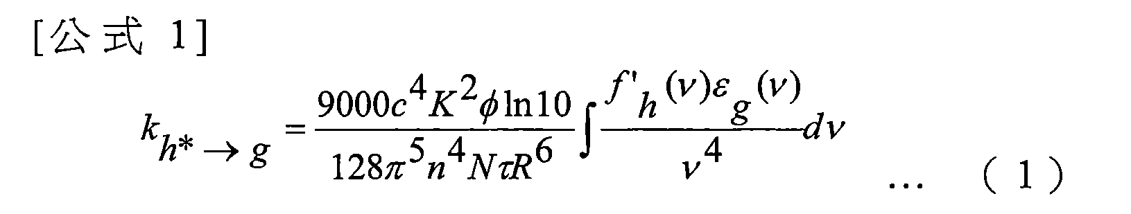
在公式1中,ν表示振盪數,f’h(ν)表示主體材料131的正規化發射光譜(當考慮由單重激發態的能量轉移時,相當於螢光光譜,而當考慮由三重激發態的能量轉移時,相當於磷光光譜),εg(ν)表示客體材料132的莫耳吸光係數,N表示亞佛加厥數,n表示介質的折射率,R表示主體材料131與客體材料132的分子間距,τ表示所測量的激發態的壽命(螢光壽命或磷光壽命),c表示光速,Φ表示發光量子產率(當考慮由單重激發態的能量轉移時,相當於螢光量子產率,而當考慮由三重激發態的能量轉移時,相當於磷光量子產率),K2表示主體材料131和客體材料132的躍遷偶極矩的配向的係數(0至4)。此外,在無規配向中,K2=2/3。
In
《德克斯特機制》 "Dexter Mechanism"
在德克斯特機制中,主體材料131和客體材料132接近於產生軌域的重疊的接觸有效距離,藉由交換激發態的主體材料131的電子和基態的客體材料132的電子,發生能量轉移。另外,公式2示出德克斯特機制的速度常數kh*→g。
In the Dexter mechanism, the
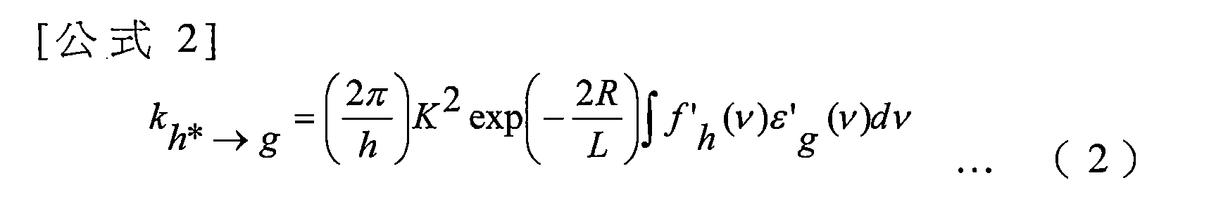
在公式2中,h表示普朗克常數,K表示具有能量維數(energy dimension)的常數,ν表示振盪數,f’h(ν)表示主體材料131的正規化發射光譜(當考慮由單重激發態的能量轉移時,相當於螢光光譜,而當考慮由三重激發態的能量轉移時,相當於磷光光譜),ε‘g(ν)表示客體材料132的正規化吸收光譜,L表示有效分子半徑,R表示主體材料131與客體材料132的分子間距。
In
在此,從主體材料131到客體材料132的能量轉移效率ΦET以公式3表示。kr表示主體材料131的發光過程(當考慮由單重激發態的能量轉移時,相當於螢光,而當考慮由三重激發態的能量轉移時,相當於磷光)的速度常數,kn表示主體材料131的非發光過程(熱失活或系間跨越)的速度常數,τ表示所測量的主體材料131的激發態的壽命。
Here, the energy transfer efficiency Φ ET from the
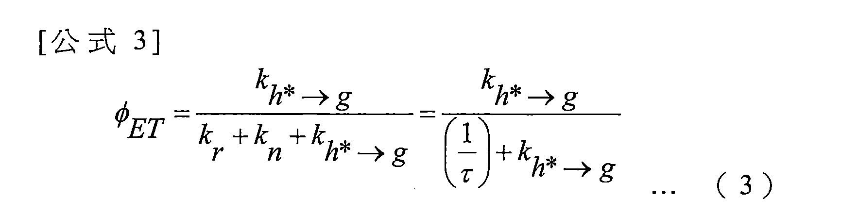
從公式3可知,為了提高能量轉移效率ΦET,增大能量轉移的速度常數kh*→g,其他競爭的速度常數kr+kn(=1/τ)相對變小,即可。 From Formula 3, we can know that in order to improve the energy transfer efficiency Φ ET , the speed constant of energy transfer k h*→g is increased, and the speed constants of other competitions k r +k n (=1/τ) are relatively reduced.
《用來提高能量轉移的概念》 "Concepts for enhancing energy transfer"
首先,考慮基於福斯特機制的能量轉移。藉由將公式1代入到公式3,可以消去τ。因此,在福斯特機制中,能量轉移效率ΦET不取決於主體材料131的激發態的壽命τ。另外,當發光量子產率Φ(因為是關於來自單重激發態的能量轉移的說明,所以這裡指螢光量子產率)高時,可以說能量轉移效率ΦET較高。一般而言,來自有機化合物的三重激發態的發光量子產率在室溫下非常低。因此,當主體材料131為三重激發態時,可以忽視基於福斯特機制的能量轉移過程,只需考慮主體材料131為單重激發態的情況。
First, consider the energy transfer based on the Förster mechanism. By substituting
另外,主體材料131的發射光譜(在說明來自單重激發態的能量轉移時是螢光光譜)與客體材料132的吸收光譜(相當於從單重基態到單重激發態的遷移的吸收)的重疊較佳為大。再者,客體材料132的莫耳吸光係數較佳為高。這意味著主體材料131的發射光譜與呈現在
客體材料132的最長波長一側的吸收帶重疊。注意,由於客體材料132中的從單重基態到三重激發態的直接躍遷為禁止躍遷,因此在客體材料132中,三重激發態下的莫耳吸光係數少到可以忽視的程度。由此,可以忽視基於福斯特機制的客體材料132的到三重激發態的能量轉移過程,只需考慮客體材料132的到單重激發態的能量轉移過程。也就是說,在福斯特機制中,考慮從主體材料131的單重激發態到客體材料132的單重激發態的能量轉移過程即可。
In addition, the overlap between the emission spectrum of the host material 131 (fluorescence spectrum when explaining energy transfer from the singlet excited state) and the absorption spectrum of the guest material 132 (absorption corresponding to the transition from the singlet ground state to the singlet excited state) is preferably large. Furthermore, the molar absorption coefficient of the
接著,考慮基於德克斯特機制的能量轉移。從公式2可知,為了增大速度常數kh*→g,主體材料131的發射光譜(在說明來自單重激發態的能量轉移時是螢光光譜)與客體材料132的吸收光譜(相當於從單重基態到單重激發態的遷移的吸收)的重疊較佳為大。因此,能量轉移效率的最佳化可以藉由使主體材料131的發射光譜與呈現在客體材料132的最長波長一側的吸收帶重疊而實現。
Next, consider the energy transfer based on the Dexter mechanism. From
另外,當將公式2代入到公式3時,可知德克斯特機制中的能量轉移效率ΦET取決於τ。因為德克斯特機制是基於電子交換的能量轉移過程,所以與從主體材料131的單重激發態到客體材料132的單重激發態的能量轉移同樣地,還產生從主體材料131的三重激發態到客體材料132的三重激發態的能量轉移。
In addition, when
在本發明的一個實施方式的發光元件中,客
體材料132是螢光材料,所以從主體材料131到客體材料132的三重激發態的能量轉移效率較佳為低。也就是說,從主體材料131到客體材料132的基於德克斯特機制的能量轉移效率較佳為低,而從主體材料131到客體材料132的基於福斯特機制的能量轉移效率較佳為高。
In the light-emitting element of one embodiment of the present invention, the
如上所述,基於福斯特機制的能量轉移效率不取決於主體材料131的激發態的壽命τ。另一方面,基於德克斯特機制的能量轉移效率取決於主體材料131的激發壽命τ,為了降低基於德克斯特機制的能量轉移效率,主體材料131的激發壽命τ較佳為短。
As described above, the energy transfer efficiency based on the Foster mechanism does not depend on the lifetime τ of the excited state of the
與從主體材料131到客體材料132的能量轉移同樣地,在從激態錯合物到客體材料132的能量轉移過程中也發生基於福斯特機制及德克斯特機制的兩者的能量轉移。
Similar to the energy transfer from the
於是,本發明的一個實施方式提供一種發光元件,作為主體材料131採用形成用作能夠將能量高效地轉移到客體材料132的能量施體的激態錯合物的有機化合物131_1及有機化合物131_2的組合。有機化合物131_1及有機化合物131_2所形成的激態錯合物具有彼此接近的單重激發能階與三重激發能階。因此,在發光層130中容易產生從三重激子到單重激子的遷移(反系間跨越)。因此,可以提高發光層130中的單重激子的產生效率。再者,為了使從激態錯合物的單重激發態到用作能量受體的客體材料132的單重激發態的能量轉移容易產生,較佳的
是,激態錯合物的發射光譜與客體材料132的呈現在最長波長一側(低能量一側)的吸收帶重疊。由此,可以提高客體材料132的單重激發態的產生效率。
Therefore, one embodiment of the present invention provides a light-emitting element, which uses a combination of an organic compound 131_1 and an organic compound 131_2 that form an excited complex that serves as an energy donor capable of efficiently transferring energy to a
另外,在激態錯合物所呈現的發光中,熱活化延遲螢光成分的螢光壽命較佳為短,明確而言,較佳為10ns以上且50μs以下,更佳為10ns以上且40μs以下,進一步較佳為10ns以上且30μs以下。 In addition, in the luminescence presented by the excited complex, the fluorescence lifetime of the thermally activated delayed fluorescence component is preferably short, specifically, preferably 10ns or more and 50μs or less, more preferably 10ns or more and 40μs or less, and further preferably 10ns or more and 30μs or less.
另外,在激態錯合物所呈現的發光中,熱活化延遲螢光成分所占的比例較佳為高。明確而言,在激態錯合物所呈現的發光中,熱活化延遲螢光成分所占的比率較佳為5%以上,更佳為8%以上,進一步較佳為10%以上。 In addition, the proportion of the thermally activated delayed fluorescence component in the luminescence presented by the excited complex is preferably high. Specifically, the proportion of the thermally activated delayed fluorescence component in the luminescence presented by the excited complex is preferably 5% or more, more preferably 8% or more, and further preferably 10% or more.
〈材料〉 <Material>
接著,說明根據本發明的一個實施方式的發光元件的組件。 Next, the components of the light-emitting element according to one embodiment of the present invention are described.
《發光層》 《Luminous Layer》
下面對能夠用於發光層130的材料分別進行說明。
The materials that can be used for the light-emitting
在發光層130的材料重量比中,主體材料131所占比例最大,客體材料132(螢光材料)分散於主體材料131中。發光層130的主體材料131(有機化合物131_1及有機化合物131_2)的S1能階較佳為高於發光層130的客體材料132(螢光材料)的S1能階。另外,發光
層130的主體材料131(有機化合物131_1及有機化合物131_2)的T1能階較佳為高於發光層130的客體材料132(螢光材料)的T1能階。
In the material weight ratio of the
在發光層130中,對客體材料132沒有特別的限制,但是較佳為使用蒽衍生物、稠四苯衍生物、

作為該材料,可以舉出5,6-雙[4-(10-苯基-9-蒽基)苯基]-2,2’-聯吡啶(簡稱:PAP2BPy)、5,6-雙[4’-(10-苯基-9-蒽基)聯苯-4-基]-2,2’-聯吡啶(簡稱:PAPP2BPy)、N,N’-二苯基-N,N’-雙[4-(9-苯基-9H-茀-9-基)苯基]芘-1,6-二胺(簡稱:1,6FLPAPrn)、N,N’-雙(3-甲基苯基)-N,N’-雙[3-(9-苯基-9H-茀-9-基)苯基]芘-1,6-二胺(簡稱:1,6mMemFLPAPrn)、N,N’-雙[4-(9H-咔唑-9-基)苯基]-N,N’-二苯基二苯乙烯-4,4’-二胺(簡稱:YGA2S)、4-(9H-咔唑-9-基)-4’-(10-苯基-9-蒽基)三苯胺(簡稱:YGAPA)、4-(9H-咔唑-9-基)-4’-(9,10-二苯基-2-蒽基)三苯胺(簡稱:2YGAPPA)、N,9-二苯基-N-[4-(10-苯基-9-蒽基)苯基]-9H-咔唑-3-胺(簡稱:PCAPA)、苝、2,5,8,11-四(三級丁基)苝(簡稱:TBP)、4-(10-苯基-9-蒽基)-4’-(9-苯基-9H-咔唑-3-基)三苯胺(簡稱:PCBAPA)、N,N”-(2-三級丁基蒽-9,10-二基二-4,1-伸苯基)雙[N,N’,N’-三苯基-1,4-苯二胺]
(簡稱:DPABPA)、N,9-二苯基-N-[4-(9,10-二苯基-2-蒽基)苯基]-9H-咔唑-3-胺(簡稱:2PCAPPA)、N-[4-(9,10-二苯基-2-蒽基)苯基]-N,N’,N’-三苯基-1,4-苯二胺(簡稱:2DPAPPA)、N,N,N’,N’,N”,N”,N''',N'''-八苯基二苯并[g,p]
作為有機化合物131_1,除了鋅、鋁類金屬錯合物以外還可以舉出


另外,可以使用如下電洞傳輸性材料及電子傳輸性材料。 In addition, the following hole-transmitting materials and electron-transmitting materials can be used.
作為電洞傳輸性材料,可以使用電洞傳輸性比電子傳輸性高的材料,較佳為使用具有1×10⁻⁶cm2/Vs以上的電洞移動率的材料。明確而言,可以使用芳族胺、咔唑衍生物、芳烴、二苯乙烯衍生物等。上述電洞傳輸性材料也可以是高分子化合物。 As the hole transport material, a material having higher hole transport than electron transport can be used, preferably a material having a hole mobility of 1×10 -6 cm 2 /Vs or more. Specifically, aromatic amines, carbazole derivatives, aromatic hydrocarbons, stilbene derivatives, etc. can be used. The hole transport material may also be a polymer compound.
作為電洞傳輸性高的材料,例如,作為芳香胺化合物,可以舉出N,N’-二(對甲苯基)-N,N’-二苯基- 對苯二胺(簡稱:DTDPPA)、4,4’-雙[N-(4-二苯胺基苯基)-N-苯胺基]聯苯(簡稱:DPAB)、N,N’-雙{4-[雙(3-甲基苯基)胺基]苯基}-N,N’-二苯基-(1,1’-聯苯)-4,4’-二胺(簡稱:DNTPD)、1,3,5-三[N-(4-二苯胺基苯基)-N-苯胺基]苯(簡稱:DPA3B)等。 As materials with high hole transport properties, for example, aromatic amine compounds include N,N'-di(p-tolyl)-N,N'-diphenyl- p-phenylenediamine (abbreviation: DTDPPA), 4,4'-bis[N-(4-diphenylaminophenyl)-N-anilino]biphenyl (abbreviation: DPAB), N,N'-bis{4-[bis(3-methylphenyl)amino]phenyl}-N,N'-diphenyl-(1,1'-biphenyl)-4,4'-diamine (abbreviation: DNTPD), and 1,3,5-tris[N-(4-diphenylaminophenyl)-N-anilino]benzene (abbreviation: DPA3B).
另外,作為咔唑衍生物,明確而言,可以舉出3-[N-(4-二苯胺基苯基)-N-苯胺基]-9-苯基咔唑(簡稱:PCzDPA1)、3,6-雙[N-(4-二苯胺基苯基)-N-苯胺基]-9-苯基咔唑(簡稱:PCzDPA2)、3,6-雙[N-(4-二苯胺基苯基)-N-(1-萘基)氨]-9-苯基咔唑(簡稱:PCzTPN2)、3-[N-(9-苯基咔唑-3-基)-N-苯胺基]-9-苯基咔唑(簡稱:PCzPCA1)、3,6-雙[N-(9-苯基咔唑-3-基)-N-苯胺基]-9-苯基咔唑(簡稱:PCzPCA2)、3-[N-(1-萘基)-N-(9-苯基咔唑-3-基)氨]-9-苯基咔唑(簡稱:PCzPCN1)等。 In addition, specific examples of carbazole derivatives include 3-[N-(4-diphenylaminophenyl)-N-anilino]-9-phenylcarbazole (abbreviated as PCzDPA1), 3,6-bis[N-(4-diphenylaminophenyl)-N-anilino]-9-phenylcarbazole (abbreviated as PCzDPA2), 3,6-bis[N-(4-diphenylaminophenyl)-N-(1-naphthyl)amino]-9-phenylcarbazole (abbreviated as PCzDPA2). CzTPN2), 3-[N-(9-phenylcarbazole-3-yl)-N-anilino]-9-phenylcarbazole (abbreviated as: PCzPCA1), 3,6-bis[N-(9-phenylcarbazole-3-yl)-N-anilino]-9-phenylcarbazole (abbreviated as: PCzPCA2), 3-[N-(1-naphthyl)-N-(9-phenylcarbazole-3-yl)amino]-9-phenylcarbazole (abbreviated as: PCzPCN1), etc.
另外,作為咔唑衍生物,還可以舉出4,4’-二(N-咔唑基)聯苯(簡稱:CBP)、1,3,5-三[4-(N-咔唑基)苯基]苯(簡稱:TCPB)、9-[4-(10-苯基-9-蒽基)苯基]-9H-咔唑(簡稱:CzPA)、1,4-雙[4-(N-咔唑基)苯基]-2,3,5,6-四苯基苯等。 In addition, carbazole derivatives include 4,4'-di(N-carbazolyl)biphenyl (abbreviated as CBP), 1,3,5-tris[4-(N-carbazolyl)phenyl]benzene (abbreviated as TCPB), 9-[4-(10-phenyl-9-anthracenyl)phenyl]-9H-carbazole (abbreviated as CzPA), and 1,4-bis[4-(N-carbazolyl)phenyl]-2,3,5,6-tetraphenylbenzene.
另外,作為芳烴,例如可以舉出2-三級丁基-9,10-二(2-萘基)蒽(簡稱:t-BuDNA)、2-三級丁基-9,10-二(1-萘基)蒽、9,10-雙(3,5-二苯基苯基)蒽(簡稱:DPPA)、2-三級丁基-9,10-雙(4-苯基苯基)蒽(簡 稱:t-BuDBA)、9,10-二(2-萘基)蒽(簡稱:DNA)、9,10-二苯基蒽(簡稱:DPAnth)、2-三級丁基蒽(簡稱:t-BuAnth)、9,10-雙(4-甲基-1-萘基)蒽(簡稱:DMNA)、2-三級丁基-9,10-雙[2-(1-萘基)苯基]蒽、9,10-雙[2-(1-萘基)苯基]蒽、2,3,6,7-四甲基-9,10-二(1-萘基)蒽、2,3,6,7-四甲基-9,10-二(2-萘基)蒽、9,9’-聯蒽、10,10’-二苯基-9,9’-聯蒽、10,10’-雙(2-苯基苯基)-9,9’-聯蒽、10,10’-雙[(2,3,4,5,6-五苯基)苯基]-9,9’-聯蒽、蒽、稠四苯、紅螢烯、苝、2,5,8,11-四(三級丁基)苝等。另外,除此之外,還可以使用稠五苯、蔻等。如此,更佳為使用具有1×10⁻⁶cm2/Vs以上的電洞移動率且碳原子數為14以上且42以下的芳烴。 Examples of aromatic hydrocarbons include 2-tert-butyl-9,10-di(2-naphthyl)anthracene (abbreviated as t-BuDNA), 2-tert-butyl-9,10-di(1-naphthyl)anthracene, 9,10-bis(3,5-diphenylphenyl)anthracene (abbreviated as DPPA), 2-tert-butyl-9,10-bis(4-phenylphenyl)anthracene (abbreviated as t-BuDBA), 9,10-di(2-naphthyl)anthracene (abbreviated as DNA), 9,10-diphenylanthracene (abbreviated as DPAnth), 2-tert-butylanthracene (abbreviated as t-BuAnth), 9,10-bis(4-methyl-1-naphthyl)anthracene (abbreviated as DMN A), 2-tert-butyl-9,10-bis[2-(1-naphthyl)phenyl]anthracene, 9,10-bis[2-(1-naphthyl)phenyl]anthracene, 2,3,6,7-tetramethyl-9,10-di(1-naphthyl)anthracene, 2,3,6,7-tetramethyl-9,10-di(2-naphthyl)anthracene, 9,9'-bianthracene, 10,10'-diphenyl-9,9'-bianthracene, 10,10'-bis(2-phenylphenyl)-9,9'-bianthracene, 10,10'-bis[(2,3,4,5,6-pentaphenyl)phenyl]-9,9'-bianthracene, anthracene, fused tetraphenyl, rubrene, perylene, 2,5,8,11-tetra(tert-butyl)perylene, etc. In addition, fused pentadiene, coronene, etc. can also be used. Thus, it is more preferable to use an aromatic hydrocarbon having a hole mobility of 1×10 -6 cm 2 /Vs or more and having 14 to 42 carbon atoms.
注意,芳烴也可以具有乙烯基骨架。作為具有乙烯基的芳烴,例如,可以舉出4,4’-雙(2,2-二苯基乙烯基)聯苯(簡稱:DPVBi)、9,10-雙[4-(2,2-二苯基乙烯基)苯基]蒽(簡稱:DPVPA)等。 Note that aromatic hydrocarbons may also have a vinyl skeleton. Examples of aromatic hydrocarbons having a vinyl group include 4,4'-bis(2,2-diphenylvinyl)biphenyl (abbreviation: DPVBi) and 9,10-bis[4-(2,2-diphenylvinyl)phenyl]anthracene (abbreviation: DPVPA).
另外,也可以使用聚(N-乙烯基咔唑)(簡稱:PVK)、聚(4-乙烯基三苯胺)(簡稱:PVTPA)、聚[N-(4-{N’-[4-(4-二苯基胺基)苯基]苯基-N’-苯基胺基}苯基)甲基丙烯醯胺](簡稱:PTPDMA)、聚[N,N’-雙(4-丁基苯基)-N,N’-雙(苯基)聯苯胺](簡稱:Poly-TPD)等高分子化合物。 In addition, high molecular weight compounds such as poly(N-vinylcarbazole) (abbreviated as PVK), poly(4-vinyltriphenylamine) (abbreviated as PVTPA), poly[N-(4-{N’-[4-(4-diphenylamino)phenyl]phenyl-N’-phenylamino}phenyl)methacrylamide] (abbreviated as PTPDMA), and poly[N,N’-bis(4-butylphenyl)-N,N’-bis(phenyl)benzidine] (abbreviated as Poly-TPD) can also be used.
另外,作為電洞傳輸性高的材料,例如,可以使用4,4’-雙[N-(1-萘基)-N-苯胺基]聯苯(簡稱: NPB或α-NPD)、N,N’-雙(3-甲基苯基)-N,N’-二苯基-[1,1’-聯苯]-4,4’-二胺(簡稱:TPD)、4,4’,4”-三(咔唑-9-基)三苯胺(簡稱:TCTA)、4,4’,4”-三[N-(1-萘基)-N-苯胺基]三苯胺(簡稱:1’-TNATA)、4,4’,4”-三(N,N-二苯胺基)三苯胺(簡稱:TDATA)、4,4’,4”-三[N-(3-甲基苯基)-N-苯胺基]三苯胺(簡稱:MTDATA)、4,4’-雙[N-(螺-9,9’-聯茀-2-基)-N-苯胺基]聯苯(簡稱:BSPB)、4-苯基-4’-(9-苯基茀-9-基)三苯胺(簡稱:BPAFLP)、4-苯基-3’-(9-苯基茀-9-基)三苯胺(簡稱:mBPAFLP)、N-(9,9-二甲基-9H-茀-2-基)-N-{9,9-二甲基-2-[N’-苯基-N’-(9,9-二甲基-9H-茀-2-基)氨]-9H-茀-7-基}苯基胺(簡稱:DFLADFL)、N-(9,9-二甲基-2-二苯胺基-9H-茀-7-基)二苯基胺(簡稱:DPNF)、2-[N-(4-二苯胺基苯基)-N-苯胺基]螺-9,9’-聯茀(簡稱:DPASF)、4-苯基-4’-(9-苯基-9H-咔唑-3-基)三苯胺(簡稱:PCBA1BP)、4,4’-二苯基-4”-(9-苯基-9H-咔唑-3-基)三苯胺(簡稱:PCBBi1BP)、4-(1-萘基)-4’-(9-苯基-9H-咔唑-3-基)三苯胺(簡稱:PCBANB)、4,4’-二(1-萘基)-4”-(9-苯基-9H-咔唑-3-基)三苯胺(簡稱:PCBNBB)、4-苯基二苯基-(9-苯基-9H-咔唑-3-基)胺(簡稱:PCA1BP)、N,N’-雙(9-苯基咔唑-3-基)-N,N’-二苯基苯-1,3-二胺(簡稱:PCA2B)、N,N’,N”-三苯基-N,N’,N”-三(9-苯基咔唑-3-基)苯-1,3,5-三胺(簡稱:PCA3B)、N-(4-聯苯)-N-(9,9-二甲基-9H-茀-2- 基)-9-苯基-9H-咔唑-3-胺(簡稱:PCBiF)、N-(1,1’-聯苯-4-基)-N-[4-(9-苯基-9H-咔唑-3-基)苯基]-9,9-二甲基-9H-茀-2-胺(簡稱:PCBBiF)、9,9-二甲基-N-苯基-N-[4-(9-苯基-9H-咔唑-3-基)苯基]茀-2-胺(簡稱:PCBAF)、N-苯基-N-[4-(9-苯基-9H-咔唑-3-基)苯基]螺-9,9’-聯茀-2-胺(簡稱:PCBASF)、2-[N-(9-苯基咔唑-3-基)-N-苯胺基]螺-9,9’-聯茀(簡稱:PCASF)、2,7-雙[N-(4-二苯胺基苯基)-N-苯胺基]-螺-9,9’-聯茀(簡稱:DPA2SF)、N-[4-(9H-咔唑-9-基)苯基]-N-(4-苯基)苯基苯胺(簡稱:YGA1BP)、N,N’-雙[4-(咔唑-9-基)苯基]-N,N’-二苯基-9,9-二甲基茀-2,7-二胺(簡稱:YGA2F)等芳香族胺化合物等。另外,可以使用3-[4-(1-萘基)-苯基]-9-苯基-9H-咔唑(簡稱:PCPN)、3-[4-(9-菲基)-苯基]-9-苯基-9H-咔唑(簡稱:PCPPn)、3,3’-雙(9-苯基-9H-咔唑)(簡稱:PCCP)、1,3-雙(N-咔唑基)苯(簡稱:mCP)、3,6-雙(3,5-二苯基苯基)-9-苯基咔唑(簡稱:CzTP)、4-{3-[3-(9-苯基-9H-茀-9-基)苯基]苯基}二苯并呋喃(簡稱:mmDBFFLBi-II)、4,4’,4”-(苯-1,3,5-三基)三(二苯并呋喃)(簡稱:DBF3P-II)、1,3,5-三(二苯并噻吩-4-基)-苯(簡稱:DBT3P-II)、2,8-二苯基-4-[4-(9-苯基-9H-茀-9-基)苯基]二苯并噻吩(簡稱:DBTFLP-III)、4-[4-(9-苯基-9H-茀-9-基)苯基]-6-苯基二苯并噻吩(簡稱:DBTFLP-IV)、4-[3-(聯伸三苯-2-基)苯基]二苯并噻吩(簡稱: mDBTPTp-II)等胺化合物、咔唑化合物、噻吩化合物、呋喃化合物、茀化合物、聯伸三苯化合物、菲化合物等。在此所述的物質主要是電洞移動率為1×10⁻⁶cm2/Vs以上的物質。但是,只要是電洞傳輸性高於電子傳輸性的物質,就可以使用上述物質以外的物質。 In addition, as a material with high hole transport properties, for example, 4,4'-bis[N-(1-naphthyl)-N-anilino]biphenyl (abbreviated as NPB or α-NPD), N,N'-bis(3-methylphenyl)-N,N'-diphenyl-[1,1'-biphenyl]-4,4'-diamine (abbreviated as TPD), 4,4',4"-tris(carbazol-9-yl)triphenylamine (abbreviated as TCTA), 4,4',4"-tris[N-(1-naphthyl)-N-anilino]triphenylamine (abbreviated as 1'-TNATA), 4,4',4"-tris(N,N-diphenylamino)triphenylamine (abbreviated as TDATA), 4,4',4"-tris[N-(3-methylphenyl)-N-anilino]triphenylamine (abbreviated as MTDATA), 4,4'-Bis[N-(spiro-9,9'-bifluoren-2-yl)-N-anilino]biphenyl (BSPB), 4-phenyl-4'-(9-phenylfluoren-9-yl)triphenylamine (BPAFLP), 4-phenyl-3'-(9-phenylfluoren-9-yl)triphenylamine (mBPAFLP), N-(9,9-dimethyl-9H-fluoren-2-yl)-N-{9,9-dimethyl-2-[N'-phenyl-N'-(9,9-dimethyl-9H-fluoren-2-yl)amino]-9H-fluoren-7-yl}phenylamine (DFLADFL), N-(9,9 -dimethyl-2-diphenylamino-9H-fluoren-7-yl)diphenylamine (abbreviated as DPNF), 2-[N-(4-diphenylaminophenyl)-N-phenylamino]spiro-9,9'-bifluoren-7-yl (abbreviated as DPASF), 4-phenyl-4'-(9-phenyl-9H-carbazole-3-yl)triphenylamine (abbreviated as PCBA1BP), 4,4'-diphenyl-4"-(9-phenyl-9H-carbazole-3-yl)triphenylamine (abbreviated as PCBBi1BP), 4-(1-naphthyl)-4'-(9-phenyl-9H-carbazole-3-yl)triphenylamine (abbreviated as PCBANB), 4,4 '-Di(1-naphthyl)-4"-(9-phenyl-9H-carbazole-3-yl)triphenylamine (abbreviated as: PCBNBB), 4-phenyldiphenyl-(9-phenyl-9H-carbazole-3-yl)amine (abbreviated as: PCA1BP), N,N'-bis(9-phenylcarbazole-3-yl)-N,N'-diphenylbenzene-1,3-diamine (abbreviated as: PCA2B), N,N',N"-triphenyl-N,N',N"-tri(9-phenylcarbazole-3-yl)benzene-1,3,5-triamine (abbreviated as: PCA3B), N-(4-biphenyl)-N-(9,9-dimethyl-9H-fluorene-2-yl)amine 9,9-dimethyl-N-phenyl-N-[4-(9-phenyl-9H-carbazole-3-yl)phenyl]fluoren-2-amine (PCBAF), N-phenyl-N-[4-(9-phenyl-9H-carbazole-3-yl)phenyl]spiro-9,9'-bifluoren-2-amine (PCBASF) ), 2-[N-(9-phenylcarbazole-3-yl)-N-anilino]spiro-9,9'-bifluorene (abbreviated as: PCASF), 2,7-bis[N-(4-diphenylaminophenyl)-N-anilino]-spiro-9,9'-bifluorene (abbreviated as: DPA2SF), N-[4-(9H-carbazole-9-yl)phenyl]-N-(4-phenyl)phenylaniline (abbreviated as: YGA1BP), N,N'-bis[4-(carbazole-9-yl)phenyl]-N,N'-diphenyl-9,9-dimethylfluorene-2,7-diamine (abbreviated as: YGA2F) and other aromatic amine compounds. In addition, 3-[4-(1-naphthyl)-phenyl]-9-phenyl-9H-carbazole (abbreviated as PCPN), 3-[4-(9-phenanthrenyl)-phenyl]-9-phenyl-9H-carbazole (abbreviated as PCPPn), 3,3'-bis(9-phenyl-9H-carbazole) (abbreviated as PCCP), 1,3-bis(N-carbazolyl)benzene (abbreviated as mCP), 3,6-bis(3,5-diphenylphenyl)-9-phenylcarbazole (abbreviated as CzTP), 4-{3-[3-(9-phenyl-9H-fluoren-9-yl)phenyl]phenyl}dibenzofuran (abbreviated as mmDBFFLB) can be used. i-II), 4,4',4"-(Benzene-1,3,5-triyl)tri(dibenzofuran) (abbreviated as DBF3P-II), 1,3,5-tri(dibenzothiophene-4-yl)-benzene (abbreviated as DBT3P-II), 2,8-diphenyl-4-[4-(9-phenyl-9H-fluoren-9-yl)phenyl]dibenzothiophene (abbreviated as DBTFLP-III), 4-[4-(9-phenyl-9H-fluoren-9-yl)phenyl]-6-phenyldibenzothiophene (abbreviated as DBTFLP-IV), 4-[3-(triphenyl-2-yl)phenyl]dibenzothiophene (abbreviated as DBTFLP-IV), The substances mentioned here are mainly substances with a hole mobility of 1×10 -6 cm 2 /Vs or more. However, substances other than the above substances may be used as long as the hole transport property is higher than the electron transport property.
作為電子傳輸性材料,可以使用電子傳輸性比電洞傳輸性高的材料,較佳為使用具有1×10⁻⁶cm2/Vs以上的電子移動率的材料。作為容易接收電子的材料(具有電子傳輸性的材料),可以使用含氮雜芳族化合物等缺π電子型雜芳族化合物或金屬錯合物等。明確而言,可以舉出包括喹啉配體、苯并喹啉配體、

作為具有喹啉骨架或苯并喹啉骨架的金屬錯合物,例如有三(8-羥基喹啉)鋁(III)(簡稱:Alq)、三(4-甲基-8-羥基喹啉)鋁(III)(簡稱:Almq3)、雙(10-羥基苯并[h]喹啉)鈹(II)(簡稱:BeBq2)、雙(2-甲基-8-羥基喹啉)(4-苯基苯酚)鋁(III)(簡稱:BAlq)、雙(8-羥基喹啉)鋅(II)(簡稱:Znq)等。另外,除此之外,還可以使用如雙[2-(2-苯并


作為有機化合物131_2,採用能夠與有機化合物131_1形成激態錯合物的組合。明確而言,可以使用如上所示的電洞傳輸性材料及電子傳輸性材料。此時,較佳為以由有機化合物131_1與有機化合物131_2形成的激態錯合物的發光峰值與客體材料132(螢光材料)的最長波長一側(低能量一側)的吸收帶重疊的方式選擇有機化合物131_1、有機化合物131_2及客體材料132(螢光材料)。由此,可以實現一種發光效率得到顯著提高的發光元件。 As the organic compound 131_2, a combination capable of forming an excited complex with the organic compound 131_1 is used. Specifically, the hole-transmitting material and the electron-transmitting material shown above can be used. At this time, it is preferable to select the organic compound 131_1, the organic compound 131_2, and the guest material 132 (fluorescent material) in such a way that the luminescence peak of the excited complex formed by the organic compound 131_1 and the organic compound 131_2 overlaps with the absorption band of the longest wavelength side (low energy side) of the guest material 132 (fluorescent material). Thus, a light-emitting element with significantly improved luminescence efficiency can be realized.
作為發光層130所包括的主體材料131(有機化合物131_1及有機化合物131_2),可以使用具有將三
重激發能轉換為單重激發能的功能的材料。作為該具有將三重激發能轉換為單重激發能的功能的材料,除了激態錯合物之外,可以舉出熱活化延遲螢光(Thermally activated delayed fluorescence:TADF)材料。因此,可以將有關激態錯合物的記載看作有關熱活化延遲螢光材料的記載。注意,熱活化延遲螢光材料是指三重激發能階與單重激發能階的差較小且具有藉由反系間跨越將能量從三重激發態轉換為單重激發態的功能的材料。因此,能夠藉由微小的熱能量將三重激發態上轉換(up-convert)為單重激發態(反系間跨越)並能夠高效地呈現來自單重激發態的發光(螢光)。另外,可以高效地獲得熱活化延遲螢光的條件為如下:三重激發態能階與單重激態發能階的能量差大於0eV且為0.2eV以下,較佳為大於0eV且為0.1eV以下。
As the host material 131 (organic compound 131_1 and organic compound 131_2) included in the light-emitting
另外,呈現熱活化延遲螢光的材料也可以是單獨地藉由反系間跨越由三重激發態產生單重激發態的材料。當熱活化延遲螢光材料由一種材料構成時,例如可以使用如下材料。 In addition, the material exhibiting thermally activated delayed fluorescence may also be a material that generates a singlet excited state from a triplet excited state by anti-system crossing alone. When the thermally activated delayed fluorescence material is composed of one material, for example, the following materials can be used.
首先,可以舉出富勒烯或其衍生物、原黃素等吖啶衍生物、曙紅(eosin)等。此外,可以舉出包含鎂(Mg)、鋅(Zn)、鎘(Cd)、錫(Sn)、鉑(Pt)、銦(In)或鈀(Pd)等的含金屬紫質。作為該含金屬紫質,例如也可以舉出原紫質-氟化錫錯合物(SnF2(Proto IX))、中紫質-氟化錫錯合物(SnF2(Meso IX))、血紫質-氟化錫錯合物(SnF2(Hemato IX))、糞紫質四甲 基酯-氟化錫錯合物(SnF2(Copro III-4Me))、八乙基紫質-氟化錫錯合物(SnF2(OEP))、初紫質-氟化錫錯合物(SnF2(Etio I))、八乙基紫質-氯化鉑錯合物(PtCl2OEP)等。 First, fullerene or its derivatives, acridine derivatives such as proflavine, eosin, etc. can be cited. In addition, metal-containing porphyrins containing magnesium (Mg), zinc (Zn), cadmium (Cd), tin (Sn), platinum (Pt), indium (In), or palladium (Pd) can be cited. Examples of the metal-containing porphyrin include protoporphyrin-tin fluoride complex (SnF 2 (Proto IX)), mesoporphyrin-tin fluoride complex (SnF 2 (Meso IX)), hematoporphyrin-tin fluoride complex (SnF 2 (Hemato IX)), naphthalene tetramethyl ester-tin fluoride complex (SnF 2 (Copro III-4Me)), octaethylporphyrin-tin fluoride complex (SnF 2 (OEP)), orthoporphyrin-tin fluoride complex (SnF 2 (Etio I)), and octaethylporphyrin-platinum chloride complex (PtCl 2 OEP).
另外,作為由一種材料構成的熱活化延遲螢光材料,還可以使用具有富π電子型芳雜環及缺π電子型芳雜環的雜環化合物。明確而言,可以舉出2-(聯苯-4-基)-4,6-雙(12-苯基吲哚并[2,3-a]咔唑-11-基)-1,3,5-三嗪(簡稱:PIC-TRZ)、2-{4-[3-(N-苯基-9H-咔唑-3-基)-9H-咔唑-9-基]苯基}-4,6-二苯基-1,3,5-三嗪(簡稱:PCCzPTzn)、2-[4-(10H-吩惡嗪-10-基)苯基]-4,6-二苯基-1,3,5-三嗪(簡稱:PXZ-TRZ)、3-[4-(5-苯基-5,10-二氫啡
發光層130也可以由兩層以上的多個層形
成。例如,在從電洞傳輸層一側依次層疊第一發光層和第二發光層來形成發光層130的情況下,可以將具有電洞傳輸性的物質用作第一發光層的主體材料,並且將具有電子傳輸性的物質用作第二發光層的主體材料。
The light-emitting
另外,發光層130中也可以包括主體材料131及客體材料132以外的材料。
In addition, the light-emitting
《一對電極》 "A pair of electrodes"
電極101及電極102具有對發光層130注入電洞及電子的功能。電極101及電極102可以使用金屬、合金、導電性化合物以及它們的混合物或疊層體等形成。金屬的典型例子是鋁(Al),除此之外,可以使用銀(Ag)、鎢、鉻、鉬、銅、鈦等過渡金屬;鋰(Li)或銫等鹼金屬;鈣或鎂(Mg)等第2族金屬。作為過渡金屬,也可以使用鐿(Yb)等稀土金屬。作為合金,可以使用包括上述金屬的合金,例如可以舉出MgAg、AlLi等。作為導電性化合物,例如,可以舉出銦錫氧化物(Indium Tin Oxide,以下稱為ITO)、包含矽或氧化矽的銦錫氧化物(簡稱:ITSO)、銦鋅氧化物(Indium Zinc Oxide)、包含鎢及鋅的銦氧化物等金屬氧化物。作為導電性化合物也可以使用石墨烯等無機碳類材料。如上所述,可以藉由層疊多個這些材料形成電極101和電極102中的一個或兩個。
The
另外,從發光層130獲得的發光透過電極101和電極102中的一個或兩個被提取。因此,電極101和電極102中的至少一個具有使可見光透過的功能。作為具有透光
功能的導電性材料,可以舉出可見光的穿透率為40%以上且100%以下,較佳為60%以上且100%以下,且電阻率為1×10⁻²Ω.cm以下的導電性材料。另外,提取光一側的電極也可以是由具有透光的功能及反射光的功能的導電性材料形成的。作為該導電性材料,可以舉出可見光的反射率為20%以上且80%以下,較佳為40%以上且70%以下,且電阻率為1×10⁻²Ω.cm以下的導電性材料。當將金屬或合金等透光性低的材料用於提取光的電極時,只要以能夠使可見光透過的程度的厚度(例如,1nm至10nm的厚度)形成電極101和電極102中的一個或兩個即可。
In addition, the light obtained from the light-emitting
注意,在本說明書等中,作為具有透光的功能的電極,使用具有使可見光透光的功能且具有導電性的材料即可,例如有上述以ITO(Indium Tin Oxide)為代表的氧化物導電體層、氧化物半導體層或包含有機物的有機導電體層。作為包含有機物的有機導電體層,例如可以舉出包含混合有機化合物與電子予體(施體)而成的複合材料的層、包含混合有機化合物與電子受體(受體)而成的複合材料的層等。另外,透明導電層的電阻率較佳為1×10⁵Ω.cm以下,更佳為1×10⁴Ω.cm以下。 Note that in this specification, etc., as an electrode having a light-transmitting function, a material having a function of transmitting visible light and having conductivity may be used, such as an oxide conductive layer represented by the above-mentioned ITO (Indium Tin Oxide), an oxide semiconductor layer, or an organic conductive layer containing organic substances. As an organic conductive layer containing organic substances, for example, a layer containing a composite material formed by mixing an organic compound and an electron donor (donor), a layer containing a composite material formed by mixing an organic compound and an electron acceptor (acceptor), etc. can be cited. In addition, the resistivity of the transparent conductive layer is preferably 1×10 5 Ω. cm or less, and more preferably 1×10 4 Ω. cm or less.
另外,作為電極101及電極102的成膜方法,可以適當地使用濺射法、蒸鍍法、印刷法、塗佈法、MBE(Molecular Beam Epitaxy:分子束磊晶)法、CVD法、脈衝雷射沉積法、ALD(Atomic Layer Deposition:原子層沉積)法等。
In addition, as a film forming method for the
《電洞注入層》 《Hole injection layer》
電洞注入層111具有藉由降低來自一對電極中的一個(電極101或電極102)的電洞注入能障促進電洞注入的功能,並例如使用過渡金屬氧化物、酞青衍生物或芳族胺等形成。作為過渡金屬氧化物可以舉出鉬氧化物、釩氧化物、釕氧化物、鎢氧化物、錳氧化物等。作為酞青衍生物,可以舉出酞青或金屬酞青等。作為芳族胺,可以舉出聯苯胺衍生物或伸苯基二胺衍生物等。也可以使用聚噻吩或聚苯胺等高分子化合物,典型的是:作為被自摻雜的聚噻吩的聚(乙基二氧噻吩)/聚(苯乙烯磺酸)等。
The
作為電洞注入層111,可以使用具有由電洞傳輸性材料和具有接收來自電洞傳輸性材料的電子的特性的材料構成的複合材料的層。或者,也可以使用包含具有接收電子的特性的材料的層與包含電洞傳輸性材料的層的疊層。在定態或者在存在有電場的狀態下,電荷的授受可以在這些材料之間進行。作為具有接收電子的特性的材料,可以舉出醌二甲烷衍生物、四氯苯醌衍生物、六氮雜聯伸三苯衍生物等有機受體。明確而言,可以舉出7,7,8,8-四氰基-2,3,5,6-四氟醌二甲烷(簡稱:F4-TCNQ)、氯醌、2,3,6,7,10,11-六氰-1,4,5,8,9,12-六氮雜聯伸三苯(簡稱:HAT-CN)等具有拉電子基團(鹵基或氰基)的化合物。也可以使用過渡金屬氧化物、例如第4族至第8族金屬的氧化物。明確而言,可以使用氧化釩、氧化鈮、氧化鉭、氧化鉻、氧化鉬、氧化鎢、氧化錳、氧化錸等。特別較佳
為使用氧化鉬,因為其在大氣中也穩定,吸濕性低,並且容易處理。
As the
作為電洞傳輸性材料,可以使用電洞傳輸性比電子傳輸性高的材料,較佳為使用具有1×10⁻⁶cm2/Vs以上的電洞移動率的材料。明確而言,可以使用作為能夠用於發光層130的電洞傳輸性材料而舉出的芳族胺、咔唑衍生物、芳烴、二苯乙烯衍生物等。上述電洞傳輸性材料也可以是高分子化合物。
As the hole transport material, a material having higher hole transport than electron transport can be used, and preferably a material having a hole mobility of 1×10 -6 cm 2 /Vs or more can be used. Specifically, aromatic amines, carbazole derivatives, aromatic hydrocarbons, stilbene derivatives, etc. listed as hole transport materials that can be used for the light-emitting
《電洞傳輸層》 《Hole transport layer》
電洞傳輸層112是包含電洞傳輸性材料的層,可以使用作為電洞注入層111的材料所例示的材料。電洞傳輸層112具有將注入到電洞注入層111的電洞傳輸到發光層130的功能,所以較佳為具有與電洞注入層111的HOMO能階相同或接近的HOMO能階。
The
作為上述電洞傳輸性材料,可以使用作為電洞注入層111的材料例示出的材料。另外,較佳為使用具有1×10⁻⁶cm2/Vs以上的電洞移動率的物質。但是,只要是電洞傳輸性高於電子傳輸性的物質,就可以使用上述物質以外的物質。另外,包括具有高電洞傳輸性的物質的層不限於單層,還可以層疊兩層以上的由上述物質構成的層。
As the hole-transporting material, the materials exemplified as the materials of the
《電子傳輸層》 《Electronic transmission layer》
電子傳輸層118具有將從一對電極中的另一個(電極
101或電極102)經過電子注入層119注入的電子傳輸到發光層130的功能。作為電子傳輸性材料,可以使用電子傳輸性比電洞傳輸性高的材料,較佳為使用具有1×10⁻⁶cm2/Vs以上的電子移動率的材料。作為容易接收電子的化合物(具有電子傳輸性的材料),可以使用含氮雜芳族化合物等缺π電子型雜芳族化合物或金屬錯合物等。明確而言,可以舉出作為可用於發光層130的電子傳輸性材料而舉出的包括喹啉配體、苯并喹啉配體、

另外,還可以在電子傳輸層118與發光層130之間設置控制電子載子的移動的層。該層是對上述電子傳輸性高的材料添加少量的電子俘獲性高的物質的層,藉由抑制電子載子的移動,可以調節載子的平衡。這種結構對抑制因電子穿過發光層而引起的問題(例如元件壽命的下降)發揮很大的效果。
In addition, a layer for controlling the movement of electron carriers can be provided between the
《電子注入層》 《Electron injection layer》
電子注入層119具有藉由降低來自電極102的電子注
入能障促進電子注入的功能,例如可以使用第1族金屬、第2族金屬或它們的氧化物、鹵化物、碳酸鹽等。也可以使用上述電子傳輸性材料和具有對電子傳輸性材料供應電子的特性的材料的複合材料。作為具有供電子特性的材料,可以舉出第1族金屬、第2族金屬或它們的氧化物等。明確而言,可以使用氟化鋰(LiF)、氟化銫(CsF)、氟化鈣(CaF2)及鋰氧化物(LiOx)等鹼金屬、鹼土金屬或這些金屬的化合物。另外,可以使用氟化鉺(ErF3)等稀土金屬化合物。另外,也可以將電子鹽用於電子注入層119。作為該電子鹽,例如可以舉出對鈣和鋁的混合氧化物以高濃度添加電子的物質等。另外,也可以將能夠用於電子傳輸層118的物質用於電子注入層119。
The
另外,也可以將有機化合物與電子予體(施體)混合形成的複合材料用於電子注入層119。這種複合材料因為藉由電子予體在有機化合物中產生電子而具有優異的電子注入性和電子傳輸性。在此情況下,有機化合物較佳為在傳輸所產生的電子方面性能優異的材料,明確而言,例如,可以使用如上所述的構成電子傳輸層118的物質(金屬錯合物、雜芳族化合物等)。作為電子予體,只要是對有機化合物呈現電子供給性的物質即可。明確而言,較佳為使用鹼金屬、鹼土金屬和稀土金屬,可以舉出鋰、銫、鎂、鈣、鉺、鐿等。另外,較佳為使用鹼金屬氧化物或鹼土金屬氧化物,可以舉出鋰氧化物、鈣氧化物、鋇氧化物等。此外,還可以使用氧化鎂等路易士鹼。另
外,也可以使用四硫富瓦烯(簡稱:TTF)等有機化合物。
In addition, a composite material formed by mixing an organic compound with an electron donor can also be used for the
另外,上述發光層、電洞注入層、電洞傳輸層、電子傳輸層及電子注入層都可以藉由蒸鍍法(包括真空蒸鍍法)、噴墨法、塗佈法、凹版印刷等方法形成。此外,作為上述發光層、電洞注入層、電洞傳輸層、電子傳輸層及電子注入層,除了上述材料之外,也可以使用量子點等無機化合物或高分子化合物(低聚物、樹枝狀聚合物、聚合物等)。 In addition, the above-mentioned luminescent layer, hole injection layer, hole transport layer, electron transport layer and electron injection layer can be formed by evaporation (including vacuum evaporation), inkjet, coating, gravure printing and other methods. In addition, as the above-mentioned luminescent layer, hole injection layer, hole transport layer, electron transport layer and electron injection layer, in addition to the above-mentioned materials, inorganic compounds such as quantum dots or polymer compounds (oligomers, dendrimers, polymers, etc.) can also be used.
作為量子點,可以使用膠狀量子點、合金型量子點、核殼(Core Shell)型量子點、核型量子點等。另外,也可以使用包含2族與16族、13族與15族、13族與17族、11族與17族或14族與15族的元素群的量子點。或者,可以使用包含鎘(Cd)、硒(Se)、鋅(Zn)、硫(S)、磷(P)、銦(In)、碲(Te)、鉛(Pb)、鎵(Ga)、砷(As)、鋁(Al)等元素的量子點。
As quantum dots, colloidal quantum dots, alloy quantum dots, core-shell quantum dots, core-type quantum dots, etc. can be used. In addition, quantum dots containing element groups of
《基板》 《Substrate》
另外,本發明的一個實施方式的發光元件可以在由玻璃、塑膠等構成的基板上製造。作為在基板上層疊的順序,既可以從電極101一側依次層疊又可以從電極102一側依次層疊。
In addition, the light-emitting element of one embodiment of the present invention can be manufactured on a substrate made of glass, plastic, etc. As the order of stacking on the substrate, it can be stacked in sequence from the
另外,作為能夠形成本發明的一個實施方式 的發光元件的基板,例如可以使用玻璃、石英或塑膠等。或者,也可以使用撓性基板。撓性基板是可以彎曲的基板,例如由聚碳酸酯、聚芳酯製成的塑膠基板等。另外,可以使用薄膜、藉由蒸鍍形成的無機薄膜等。注意,只要在發光元件及光學元件的製造過程中起支撐物的作用,就可以使用其他材料。或者,只要具有保護發光元件及光學元件的功能即可。 In addition, as a substrate of a light-emitting element capable of forming an embodiment of the present invention, for example, glass, quartz or plastic can be used. Alternatively, a flexible substrate can also be used. A flexible substrate is a substrate that can be bent, such as a plastic substrate made of polycarbonate or polyarylate. In addition, a thin film, an inorganic film formed by evaporation, etc. can be used. Note that other materials can be used as long as they serve as a support in the manufacturing process of the light-emitting element and the optical element. Alternatively, as long as they have the function of protecting the light-emitting element and the optical element, it will be fine.
例如,在本發明等中,可以使用各種基板形成發光元件。對基板的種類沒有特別的限制。作為該基板的例子,例如可以使用半導體基板(例如,單晶基板或矽基板)、SOI基板、玻璃基板、石英基板、塑膠基板、金屬基板、不鏽鋼基板、具有不鏽鋼箔的基板、鎢基板、具有鎢箔的基板、撓性基板、貼合薄膜、包含纖維狀的材料的紙或者基材薄膜等。作為玻璃基板的例子,有鋇硼矽酸鹽玻璃、鋁硼矽酸鹽玻璃、鈉鈣玻璃等。作為撓性基板、貼合薄膜、基材薄膜等,可以舉出如下例子。例如,可以舉出以聚對苯二甲酸乙二醇酯(PET)、聚萘二甲酸乙二醇酯(PEN)、聚醚碸(PES)、聚四氟乙烯(PTFE)為代表的塑膠。或者,作為例子,可以舉出丙烯酸樹脂等樹脂等。或者,作為例子,可以舉出聚丙烯、聚酯、聚氟化乙烯或聚氯乙烯等。或者,作為例子,可以舉出聚醯胺、聚醯亞胺、芳族聚醯胺、環氧樹脂、無機蒸鍍薄膜、紙類等。 For example, in the present invention, etc., various substrates can be used to form light-emitting elements. There is no particular limitation on the type of substrate. As examples of the substrate, for example, a semiconductor substrate (for example, a single crystal substrate or a silicon substrate), an SOI substrate, a glass substrate, a quartz substrate, a plastic substrate, a metal substrate, a stainless steel substrate, a substrate with a stainless steel foil, a tungsten substrate, a substrate with a tungsten foil, a flexible substrate, a bonding film, paper containing a fibrous material, or a base film can be used. Examples of glass substrates include barium borosilicate glass, aluminum borosilicate glass, sodium calcium glass, and the like. As examples of flexible substrates, bonding films, base films, and the like, the following examples can be cited. For example, plastics represented by polyethylene terephthalate (PET), polyethylene naphthalate (PEN), polyether sulfone (PES), and polytetrafluoroethylene (PTFE) can be cited. Alternatively, resins such as acrylic resins can be cited as examples. Alternatively, polypropylene, polyester, polyvinyl fluoride, or polyvinyl chloride can be cited as examples. Alternatively, polyamide, polyimide, aromatic polyamide, epoxy resin, inorganic vapor-deposited film, paper, etc. can be cited as examples.
另外,也可以作為基板使用撓性基板,並在 撓性基板上直接形成發光元件。或者,也可以在基板與發光元件之間設置剝離層。當剝離層上製造發光元件的一部分或全部,然後將其從基板分離並轉置到其他基板上時可以使用剝離層。此時,也可以將發光元件轉置到耐熱性低的基板或撓性基板上。另外,作為上述剝離層,例如可以使用鎢膜和氧化矽膜的無機膜的疊層結構或在基板上形成有聚醯亞胺等樹脂膜的結構等。 In addition, a flexible substrate may be used as a substrate, and a light-emitting element may be formed directly on the flexible substrate. Alternatively, a peeling layer may be provided between the substrate and the light-emitting element. The peeling layer may be used when a part or all of the light-emitting element is manufactured on the peeling layer, and then it is separated from the substrate and transferred to another substrate. In this case, the light-emitting element may also be transferred to a substrate or a flexible substrate with low heat resistance. In addition, as the above-mentioned peeling layer, for example, a stacked structure of an inorganic film of a tungsten film and a silicon oxide film or a structure in which a resin film such as polyimide is formed on a substrate may be used.
也就是說,也可以使用一個基板來形成發光元件,然後將發光元件轉置到另一個基板上。作為發光元件被轉置的基板的例子,除了上述基板之外,還可以舉出玻璃紙基板、石材基板、木材基板、布基板(包括天然纖維(絲、棉、麻)、合成纖維(尼龍、聚氨酯、聚酯)或再生纖維(醋酯纖維、銅氨纖維、人造纖維、再生聚酯)等)、皮革基板、橡膠基板等。藉由採用這些基板,可以製造不易損壞的發光元件、耐熱性高的發光元件、實現輕量化的發光元件或實現薄型化的發光元件。 That is, a light-emitting element can be formed using one substrate and then transferred to another substrate. As examples of substrates to which light-emitting elements are transferred, in addition to the above-mentioned substrates, there can be cited glass paper substrates, stone substrates, wood substrates, cloth substrates (including natural fibers (silk, cotton, linen), synthetic fibers (nylon, polyurethane, polyester) or recycled fibers (acetate, cuprammonium, rayon, recycled polyester), etc.), leather substrates, rubber substrates, etc. By using these substrates, it is possible to manufacture light-emitting elements that are not easily damaged, light-emitting elements with high heat resistance, light-emitting elements that are lightweight, or light-emitting elements that are thin.
另外,也可以在上述基板上例如形成場效應電晶體(FET),並且在與FET電連接的電極上製造發光元件250。由此,可以製造藉由FET控制發光元件的驅動的主動矩陣型顯示裝置。
In addition, a field effect transistor (FET) may be formed on the substrate, and a light-emitting
在本實施方式中,對本發明的一個實施方式進行說明。此外,在其他實施方式中,將對本發明的一個實施方式進行說明。但是,本發明的一個實施方式不侷限於此。例如,在本發明的一個實施方式中,示出了主體材 料包括第一有機化合物及第二有機化合物的情況的例子,但是本發明的一個實施方式並不侷限於此。根據情況或狀況,在本發明的一個實施方式中,例如,主體材料也可以不包括第一有機化合物或第二有機化合物。或者,例如,在本發明的一個實施方式中,示出了激態錯合物包含螢光壽命為10ns以上且50μs以下的延遲螢光成分的情況的例子,但是本發明的一個實施方式並不侷限於此。根據情況或狀況,在本發明的一個實施方式中,例如,激態錯合物也可以包括螢光壽命小於10ns的延遲螢光成分。或者,例如,激態錯合物也可以包括螢光壽命大於50μs的延遲螢光成分。或者,例如,雖然本發明的一個實施方式例示出在激態錯合物所呈現的發光中延遲螢光成分所占的比率為5%以上的情況,但是本發明的一個實施方式並不侷限於此。根據情形或狀況,在本發明的一個實施方式中,例如,在激態錯合物所呈現的發光中延遲螢光成分所占的比率也可以低於5%。 In this embodiment, one embodiment of the present invention is described. In addition, in other embodiments, one embodiment of the present invention is described. However, one embodiment of the present invention is not limited thereto. For example, in one embodiment of the present invention, an example is shown in which the host material includes the first organic compound and the second organic compound, but one embodiment of the present invention is not limited thereto. Depending on the situation or condition, in one embodiment of the present invention, for example, the host material may not include the first organic compound or the second organic compound. Or, for example, in one embodiment of the present invention, an example is shown in which the excited complex includes a delayed fluorescent component having a fluorescent lifetime of 10 ns or more and 50 μs or less, but one embodiment of the present invention is not limited thereto. According to circumstances or conditions, in one embodiment of the present invention, for example, the excited state complex may also include a delayed fluorescence component having a fluorescence lifetime of less than 10ns. Or, for example, the excited state complex may also include a delayed fluorescence component having a fluorescence lifetime of greater than 50μs. Or, for example, although one embodiment of the present invention illustrates a case where the delayed fluorescence component accounts for more than 5% of the luminescence presented by the excited state complex, one embodiment of the present invention is not limited thereto. According to circumstances or conditions, in one embodiment of the present invention, for example, the delayed fluorescence component accounts for less than 5% of the luminescence presented by the excited state complex.
本實施方式所示的結構可以與其他實施方式所示的結構適當地組合而實施。 The structure shown in this embodiment can be implemented in combination with the structures shown in other embodiments as appropriate.
實施方式2
在本實施方式中,參照圖2A至圖3C對與實施方式1所示的結構不同的結構的發光元件及該發光元件的發光機制進行說明。注意,在圖2A至圖3C中使用與圖1A相同的陰影線示出具有與圖1A相同的功能的部分,而有時省
略元件符號。此外,具有與圖1A相同的功能的部分由相同的元件符號表示,有時省略其詳細說明。
In this embodiment, a light-emitting element having a structure different from that shown in
〈發光元件的結構例子1〉 <Structural example 1 of light-emitting element>
圖2A是發光元件260的剖面示意圖。 FIG2A is a schematic cross-sectional view of the light-emitting element 260.
圖2A所示的發光元件260在一對電極(電極101與電極102)之間具有多個發光單元(圖2A中的發光單元106和發光單元108)。一個發光單元具有與圖1A所示的EL層100同樣的結構。也就是說,圖1A所示的發光元件250具有一個發光單元,而發光元件260具有多個發光單元。注意,在發光元件260中,雖然對電極101為陽極且電極102為陰極時的情況進行說明,但是作為發光元件260的結構也可以採用與此相反的結構。
The light-emitting element 260 shown in FIG2A has a plurality of light-emitting units (light-emitting unit 106 and light-emitting unit 108 in FIG2A) between a pair of electrodes (
另外,在圖2A所示的發光元件260中,層疊有發光單元106和發光單元108,並且在發光單元106與發光單元108之間設置有電荷產生層115。另外,發光單元106和發光單元108可以具有相同結構或不同結構。例如,較佳為將圖1A所示的EL層100用於發光單元108。
In addition, in the light-emitting element 260 shown in FIG. 2A , the light-emitting unit 106 and the light-emitting unit 108 are stacked, and the
另外,發光元件260包括發光層120和發光層130。另外,發光單元106除了發光層120之外還包括電洞注入層111、電洞傳輸層112、電子傳輸層113及電子注入層114。此外,發光單元108除了發光層130之外還包括電洞注入層116、電洞傳輸層117、電子傳輸層118及電子注入層119。
In addition, the light-emitting element 260 includes a light-emitting
電荷產生層115既可以具有對電洞傳輸性材料添加有作為電子受體的受體性物質的結構,也可以具有對電子傳輸性材料添加有作為電子予體的施體性物質的結構。另外,也可以層疊這兩種結構。
The
當電荷產生層115包含有機化合物與受體性物質的複合材料時,作為該複合材料使用可以用於實施方式1所示的電洞注入層111的複合材料即可。作為有機化合物,可以使用芳香胺化合物、咔唑化合物、芳烴、高分子化合物(低聚物、樹枝狀聚合物、聚合物等)等各種化合物。另外,作為有機化合物,較佳為使用其電洞移動率為1×10⁻⁶cm2/Vs以上的物質。但是,只要是其電洞傳輸性高於電子傳輸性的物質,就可以使用這些以外的材料。因為由有機化合物和受體性物質構成的複合材料具有良好的載子注入性以及載子傳輸性,所以可以實現低電壓驅動以及低電流驅動。注意,如發光單元108,在發光單元的陽極一側的表面接觸於電荷產生層115時,電荷產生層115還可以具有發光單元的電洞注入層或電洞傳輸層的功能,所以在該發光單元中也可以不設置電洞注入層或電洞傳輸層。
When the
注意,電荷產生層115也可以是組合包含有機化合物和受體性物質的複合材料的層與由其他材料構成的層的疊層結構。例如,也可以是組合包含有機化合物和受體性物質的複合材料的層與包含選自供電子性物質中的一個化合物和高電子傳輸性的化合物的層的結構。另外,
也可以是組合包含有機化合物和受體性物質的複合材料的層與包含透明導電材料的層的結構。
Note that the
夾在發光單元106與發光單元108之間的電荷產生層115只要具有在將電壓施加到電極101和電極102之間時,將電子注入到一個發光單元且將電洞注入到另一個發光單元的結構即可。例如,在圖2A中,在以使電極101的電位高於電極102的電位的方式施加電壓時,電荷產生層115將電子注入到發光單元106且將電洞注入到發光單元108。
The
從光提取效率的觀點來看,電荷產生層115較佳為具有可見光透射性(明確而言,電荷產生層115具有40%以上的可見光透射率)。另外,電荷產生層115即使導電率小於一對電極(電極101及電極102)也發揮作用。
From the viewpoint of light extraction efficiency, the
當電荷產生層115的導電率與一對電極大致同樣高時,由於因電荷產生層115而產生的載子流向膜表面方向,所以有時在電極101與電極102不重疊的區域會產生發光。為了抑制這樣的不良現象,電荷產生層115較佳為由導電率低於一對電極的材料形成。
When the conductivity of the
藉由使用上述材料形成電荷產生層115,可以抑制在層疊發光層時的驅動電壓的增大。
By using the above-mentioned material to form the
雖然在圖2A中說明了具有兩個發光單元的發光元件,但是可以將同樣的結構應用於層疊有三個以上的發光單元的發光元件。如發光元件260所示,藉由在一對 電極之間以由電荷產生層將其隔開的方式配置多個發光單元,可以實現在保持低電流密度的同時還可以進行高亮度發光,並且使用壽命更長的發光元件。另外,還可以實現功耗低的發光元件。 Although FIG. 2A illustrates a light-emitting element having two light-emitting units, the same structure can be applied to a light-emitting element having three or more light-emitting units stacked. As shown in light-emitting element 260, by configuring a plurality of light-emitting units between a pair of electrodes in a manner separated by a charge generating layer, it is possible to achieve high brightness light emission while maintaining a low current density and use a light-emitting element with a longer life. In addition, a light-emitting element with low power consumption can be realized.
另外,藉由將圖1A所示的EL層100的結構應用於多個單元中的至少一個單元,可以提供一種發光效率高的發光元件。
In addition, by applying the structure of the
另外,發光單元108所包括的發光層130較佳為具有實施方式1所示的結構。由此,發光元件260作為發光材料包含螢光材料,並且成為發光效率高的發光元件,所以是較佳的。
In addition, the light-emitting
另外,如圖2B所示,發光單元108所包括的發光層120包含主體材料121和客體材料122。注意,下面以螢光材料作為客體材料122進行說明。
In addition, as shown in FIG. 2B , the light-emitting
〈〈發光層120的發光機制〉〉
〈〈Luminescence mechanism of the
下面對發光層120的發光機制進行說明。
The light-emitting mechanism of the light-emitting
從一對電極(電極101及電極102)或電荷產生層注入的電子及電洞在發光層120中再結合,由此生成激子。由於主體材料121所存在的量大於客體材料122,所以因激子的生成而形成主體材料121的激發態。
Electrons and holes injected from a pair of electrodes (
激子是指載子(電子及電洞)的對。由於激子具有能量,所以生成激子的材料成為激發態。 Excitons are pairs of carriers (electrons and holes). Since excitons have energy, the material that generates excitons becomes an excited state.
當所形成的主體材料121的激發態是單重激 發態時,單重激發能從主體材料121的S1能階移動到客體材料122的S1能階,由此形成客體材料122的單重激發態。 When the excited state of the formed host material 121 is a singlet excited state, the singlet excitation energy moves from the S1 energy level of the host material 121 to the S1 energy level of the guest material 122, thereby forming the singlet excited state of the guest material 122.
由於客體材料122是螢光材料,所以當在客體材料122中形成單重激發態時,客體材料122會迅速地發光。此時,為了得到高發光效率,客體材料122較佳為具有高螢光量子產率。另外,這在客體材料122中的載子再結合而生成的激發態為單重激發態的情況下也是同樣的。 Since the guest material 122 is a fluorescent material, when a singlet excited state is formed in the guest material 122, the guest material 122 will emit light quickly. At this time, in order to obtain high luminescence efficiency, the guest material 122 preferably has a high fluorescence quantum yield. In addition, this is also the case when the excited state generated by the recombination of carriers in the guest material 122 is a singlet excited state.
接著,對因載子的再結合而形成主體材料121的三重激發態的情況進行說明。圖2C示出此時的主體材料121與客體材料122的能階相關。另外,下面示出圖2C中的記載及元件符號。注意,由於主體材料121的T1能階較佳為低於客體材料122的T1能階,所以在圖2C中示出此時的情況,但是主體材料121的T1能階也可以高於客體材料122的T1能階。 Next, the formation of the triplet excited state of the host material 121 due to the recombination of carriers is described. FIG2C shows the energy level correlation between the host material 121 and the guest material 122 at this time. In addition, the description and component symbols in FIG2C are shown below. Note that since the T1 energy level of the host material 121 is preferably lower than the T1 energy level of the guest material 122, the situation at this time is shown in FIG2C, but the T1 energy level of the host material 121 can also be higher than the T1 energy level of the guest material 122.
.Host(121):主體材料121 .Host(121): Host material 121
.Guest(122):客體材料122(螢光材料) . Guest (122): Guest material 122 (fluorescent material)
.SFH:主體材料121的S1能階 .SFH : S1 energy level of host material 121
.TFH:主體材料121的T1能階 . TFH : T1 energy level of host material 121
.SFG:客體材料122(螢光材料)的S1能階 .SFG : S1 energy level of guest material 122 (fluorescent material)
.TFG:客體材料122(螢光材料)的T1能階 . TFG :T1 energy level of object material 122 (fluorescent material)
如圖2C所示,因三重態-三重態消滅(TTA: triplet-triplet annihilation)而由於載子的再結合生成的三重態激子彼此接近,由此產生其中一個變換為具有主體材料121的S1能階(SFH)的能量的單重態激子的反應(參照圖2C的TTA)。主體材料121的單重激發能從SFH移動到能量比其低的客體材料122的S1能階(SFG)(參照圖2C的路徑E1),形成客體材料122的單重激發態,由此客體材料122發光。 As shown in FIG2C , triplet excitons generated by the recombination of carriers due to triplet-triplet annihilation (TTA) approach each other, thereby generating a reaction in which one of the excitons is converted into a singlet exciton having energy of the S1 energy level ( SFH ) of the host material 121 (see TTA in FIG2C ). The singlet excitation energy of the host material 121 moves from SFH to the S1 energy level ( SFG ) of the guest material 122 having lower energy than the host material 121 (see path E1 in FIG2C ), forming a singlet excited state of the guest material 122, thereby causing the guest material 122 to emit light.
另外,當發光層120中的三重態激子的密度充分高(例如為1×10-12cm-3以上)時,可以忽視三重態激子的失活,而僅考慮兩個接近的三重態激子的反應。
In addition, when the density of triplet excitons in the light-emitting
另外,當在客體材料122中載子再結合而形成三重激發態時,由於客體材料122的三重激發態熱失活,所以難以將其用於發光。然而,當主體材料121的T1能階(TFH)低於客體材料122的T1能階(TFG)時,客體材料122的三重激發能能夠從客體材料122的T1能階(TFG)移動到主體材料121的T1能階(TFH)(參照圖2C的路徑E2),然後被用於TTA。 In addition, when carriers recombine to form a triplet excited state in the guest material 122, it is difficult to use it for light emission because the triplet excited state of the guest material 122 is thermally deactivated. However, when the T1 energy level ( TFH ) of the host material 121 is lower than the T1 energy level ( TFG ) of the guest material 122, the triplet excited energy of the guest material 122 can be moved from the T1 energy level ( TFG ) of the guest material 122 to the T1 energy level ( TFH ) of the host material 121 (refer to the path E2 of FIG. 2C), and then used for TTA.
也就是說,主體材料121較佳為具有利用TTA將三重激發能轉換為單重激發能的功能。由此,將在發光層120中生成的三重激發能的一部分利用主體材料121中的TTA轉換為單重激發能,並使該單重激發能移動到客體材料122,由此能夠提取螢光發光。為此,主體材料121的S1能階(SFH)較佳為高於客體材料122的S1能階(SFG)。另外,主體材料121的T1能階(TFH)較
佳為低於客體材料122的T1能階(TFG)。
That is, the host material 121 preferably has a function of converting triplet excitation energy into singlet excitation energy by TTA. Thus, a portion of the triplet excitation energy generated in the light-emitting
尤其是當客體材料122的T1能階(TFG)低於主體材料121的T1能階(TFH)時,較佳為在主體材料121與客體材料122的重量比中客體材料122所占比例較低。明確而言,對於主體材料121的客體材料122的重量比較佳為大於0且為0.05以下。由此,可以降低載子在客體材料122中再結合的概率。還可以降低從主體材料121的T1能階(TFH)到客體材料122的T1能階(TFG)的能量移動所發生的概率。 In particular, when the T1 energy level ( TFG ) of the guest material 122 is lower than the T1 energy level ( TFH ) of the host material 121, it is preferred that the proportion of the guest material 122 in the weight ratio of the host material 121 to the guest material 122 is lower. Specifically, the weight ratio of the guest material 122 to the host material 121 is preferably greater than 0 and less than 0.05. Thus, the probability of carrier recombination in the guest material 122 can be reduced. The probability of energy transfer from the T1 energy level ( TFH ) of the host material 121 to the T1 energy level ( TFG ) of the guest material 122 can also be reduced.
注意,主體材料121可以由單一的化合物構成,也可以由多個化合物構成。 Note that the main material 121 may be composed of a single compound or a plurality of compounds.
另外,在上述各結構中,用於發光單元106及發光單元108的客體材料(螢光材料)既可以相同又可以不同。當發光單元106和發光單元108包含相同的客體材料時,發光元件260成為以小電流值呈現高發光亮度的發光元件,所以是較佳的。另外,當發光單元106和發光單元108包含不同的客體材料時,發光元件260成為呈現多色發光的發光元件,所以是較佳的。尤其較佳為以實現演色性高的白色發光或至少具有紅色、綠色、藍色的發光的方式選擇客體材料。 In addition, in each of the above structures, the object materials (fluorescent materials) used for the light-emitting unit 106 and the light-emitting unit 108 can be the same or different. When the light-emitting unit 106 and the light-emitting unit 108 contain the same object material, the light-emitting element 260 becomes a light-emitting element that presents high luminance at a small current value, so it is better. In addition, when the light-emitting unit 106 and the light-emitting unit 108 contain different object materials, the light-emitting element 260 becomes a light-emitting element that presents multi-color luminescence, so it is better. It is particularly preferred to select the object material in a manner that realizes white luminescence with high color rendering or luminescence with at least red, green, and blue.
〈發光元件的結構例子2〉
<Structural example of light-emitting
圖3A是發光元件262的剖面示意圖。 FIG3A is a schematic cross-sectional view of the light-emitting element 262.
與上述發光元件260同樣地,圖3A所示的發
光元件262在一對電極(電極101與電極102)之間包括多個發光單元(在圖3A中為發光單元106及發光單元108)。一個發光單元具有與圖1A所示的EL層100同樣的結構。另外,發光單元106與發光單元108既可以是相同的結構又可以是不同的結構。
Similar to the above-mentioned light-emitting element 260, the light-emitting element 262 shown in FIG3A includes a plurality of light-emitting units (light-emitting unit 106 and light-emitting unit 108 in FIG3A) between a pair of electrodes (
另外,在圖3A所示的發光元件262中層疊有發光單元106及發光單元108,在發光單元106與發光單元108之間設置有電荷產生層115。例如,較佳為將圖1A所示的EL層100用於發光單元106。
In addition, in the light-emitting element 262 shown in FIG. 3A , the light-emitting unit 106 and the light-emitting unit 108 are stacked, and the
另外,發光元件262包括發光層130和發光層140。另外,發光單元106除了發光層130還包括電洞注入層111、電洞傳輸層112、電子傳輸層113及電子注入層114。另外,發光單元108除了發光層140還包括電洞注入層116、電洞傳輸層117、電子傳輸層118及電子注入層119。
In addition, the light-emitting element 262 includes a light-emitting
另外,發光單元108的發光層較佳為包含磷光材料。也就是說,較佳的是:發光單元106所包括的發光層130具有實施方式1所示的結構,且發光單元108所包括的發光層140具有磷光材料。下面對此時的發光元件262的結構例子進行說明。
In addition, the light-emitting layer of the light-emitting unit 108 preferably includes a phosphorescent material. In other words, it is preferred that the light-emitting
另外,如圖3B所示,發光單元108所包括的發光層140包含主體材料141和客體材料142。另外,主體材料141包含有機化合物141_1和有機化合物141_2。下面以磷光材料作為發光層140所包含的客體材料142進
行說明。
In addition, as shown in FIG. 3B , the light-emitting
〈〈發光層140的發光機制〉〉
〈〈Luminescence mechanism of the
下面,對發光層140的發光機制進行說明。
Next, the light-emitting mechanism of the light-emitting
發光層140所包含的有機化合物141_1與有機化合物141_2形成激態錯合物。
The organic compound 141_1 and the organic compound 141_2 contained in the light-emitting
發光層140中的形成激態錯合物的有機化合物141_1和有機化合物141_2的組合只要是能夠形成激態錯合物的組合即可,但較佳為其中一個是具有電洞傳輸性的化合物,而另一個是具有電子傳輸性的化合物。
The combination of the organic compound 141_1 and the organic compound 141_2 that form an excited complex in the light-emitting
圖3C示出發光層140中的有機化合物141_1、有機化合物141_2及客體材料142的能階相關。注意,下面示出圖3C中的記載及元件符號。
FIG3C shows the energy level correlation of the organic compound 141_1, the organic compound 141_2, and the guest material 142 in the light-emitting
.Host(141_1):有機化合物141_1(主體材料) .Host (141_1): Organic compound 141_1 (host material)
.Host(141_2):有機化合物141_2(主體材料) .Host (141_2): Organic compound 141_2 (host material)
.Guest(142):客體材料142(磷光材料) . Guest (142): Guest material 142 (phosphorescent material)
.SPH:有機化合物141_1(主體材料)的S1能階 . S PH : S1 energy level of organic compound 141_1 (host material)
.TPH:有機化合物141_1(主體材料)的T1能階 . T PH : T1 energy level of organic compound 141_1 (host material)
.TPG:客體材料142(磷光材料)的T1能階 . T PG : T1 energy level of guest material 142 (phosphorescent material)
.SPE:激態錯合物的S1能階 . S PE : S1 energy level of excited complex
.TPE:激態錯合物的T1能階 . T PE : T1 energy level of excited complex
由有機化合物141_1與有機化合物141_2形成的激態錯合物的單重激發態的最低能階(SPE)與激態錯合物的三重激發態的最低能階(TPE)相互鄰接(參照 圖3C的路徑C)。 The lowest energy level of the singlet excited state (S PE ) of the excited complex formed by the organic compound 141_1 and the organic compound 141_2 and the lowest energy level of the triplet excited state (T PE ) of the excited complex are adjacent to each other (refer to path C in FIG. 3C ).
然後,使激態錯合物的(SPE)和(TPE)兩者的能量移動到客體材料142(磷光材料)的三重激發態的最低能階來得到發光(參照圖3C的路徑D)。 Then, the energies of both (S PE ) and (T PE ) of the excited complex are moved to the lowest energy level of the triplet excited state of the guest material 142 (phosphorescent material) to obtain light emission (see path D in FIG. 3C ).
注意,在本說明書等中,有時將上述路徑C及路徑D的過程稱為ExTET(Exciplex-Triplet Energy Transfer:激態錯合物-三重態能量轉移)。 Note that in this manual, etc., the processes of the above-mentioned paths C and D are sometimes referred to as ExTET (Exciplex-Triplet Energy Transfer).
另外,有機化合物141_1和有機化合物141_2中的一個接收電洞,另一個接收電子來形成激態錯合物。或者,當其中一個成為激發態時與另一個相互起作用來形成激態錯合物。因此,發光層140中的幾乎所有激子都作為激態錯合物存在。由於激態錯合物的能帶間隙比有機化合物141_1及有機化合物141_2都小,所以可以以較低的激發能形成激發態。因此,藉由形成激態錯合物可以降低發光元件的驅動電壓。
In addition, one of the organic compound 141_1 and the organic compound 141_2 receives a hole, and the other receives an electron to form an excited complex. Alternatively, when one of them becomes an excited state, it interacts with the other to form an excited complex. Therefore, almost all excitons in the light-emitting
藉由作為發光層140採用上述結構,可以高效地得到來自發光層140的客體材料142(磷光材料)的發光。
By adopting the above structure as the light-emitting
另外,較佳為採用如下結構:與來自發光層140的發光的峰值相比,來自發光層130的發光的峰值更靠近短波長一側。使用呈現短波長的發光的磷光材料的發光元件有亮度劣化快的趨勢。於是,藉由作為短波長的發光採用螢光發光可以提供一種亮度劣化小的發光元件。
In addition, it is preferable to adopt the following structure: the peak of the light from the light-emitting
另外,藉由使發光層130和發光層140發射
彼此不同的發光波長的光,可以實現多色發光的元件。此時,由於合成具有不同的發光峰值的光,因此發射光譜成為具有至少兩個峰值的發射光譜。
In addition, by making the light-emitting
另外,上述結構適合用來獲得白色發光。藉由使發光層130與發光層140的光為互補色的關係,可以獲得白色發光。
In addition, the above structure is suitable for obtaining white light. By making the light of the light-emitting
另外,藉由將發光波長不同的多個發光材料用於發光層130和發光層140中的任一個或兩個,也可以得到由三原色或四種以上的發光顏色構成的演色性高的白色發光。在此情況下,也可以將發光層130和發光層140中的任一個或兩個進一步分割為層狀並使該被分割的層的每一個都含有不同的發光材料。
In addition, by using multiple luminescent materials with different luminescent wavelengths in one or both of the
〈可用於發光層的材料例子〉 〈Examples of materials that can be used for the light-emitting layer〉
下面,對可用於發光層120、發光層130及發光層140的材料進行說明。
Next, the materials that can be used for the light-emitting
〈〈可用於發光層130的材料〉〉
〈〈Materials that can be used for the light-emitting
作為能夠用於發光層130的材料,參照上述實施方式1所示的能夠用於發光層130的材料即可。由此,可以製造單重激發態的生成效率高且發光效率高的發光元件。
As a material that can be used for the light-emitting
〈〈可用於發光層120的材料〉〉
〈〈Materials that can be used for the light-emitting
在發光層120的材料重量比中,主體材料121所占比
例最大,客體材料122(螢光材料)分散在主體材料121中。較佳為主體材料121的S1能階比客體材料122(螢光材料)的S1能階高,且主體材料121的T1能階比客體材料122(螢光材料)的T1能階低。
In the material weight ratio of the light-emitting
在發光層120中,對客體材料122沒有特別限制,例如可以使用在實施方式1中作為客體材料132所例示的材料。
In the light-emitting
雖然對能夠用於發光層120中的主體材料121的材料沒有特別的限制,但是例如可以舉出:三(8-羥基喹啉)鋁(III)(簡稱:Alq)、三(4-甲基-8-羥基喹啉)鋁(III)(簡稱:Almq3)、雙(10-羥基苯并[h]喹啉)鈹(II)(簡稱:BeBq2)、雙(2-甲基-8-羥基喹啉)(4-苯基苯酚)鋁(III)(簡稱:BAlq)、雙(8-羥基喹啉)鋅(II)(簡稱:Znq)、雙[2-(2-苯并


另外,發光層120也可以由兩層以上的多個層形成。例如,在從電洞傳輸層一側依次層疊第一發光層和第二發光層來形成發光層120的情況下,可以將具有電洞傳輸性的物質用於第一發光層的主體材料,並且將具有電子傳輸性的物質用於第二發光層的主體材料。
In addition, the light-emitting
另外,在發光層120中,主體材料121既可以由一種化合物構成,又可以由多個化合物構成。或者,發光層120也可以包含主體材料121及客體材料122以外的材料。
In addition, in the light-emitting
〈〈可用於發光層140的材料〉〉
〈〈Materials that can be used for the light-emitting
在發光層140的材料重量比中,主體材料141所占比例最大,客體材料142(磷光材料)分散在主體材料141中。較佳為發光層140的主體材料141(有機化合物141_1及有機化合物141_2)的T1能階高於發光層140的客體材料(客體材料142)的T1能階。
In the material weight ratio of the light-emitting
作為有機化合物141_1,除了鋅、鋁類金屬錯合物以外還可以舉出


作為有機化合物141_2,較佳為使用可以與有機化合物141_1組合形成激態錯合物的材料。明確而言,可以使用實施方式1所示的電子傳輸性材料及電洞傳輸性材料。此時,較佳為以有機化合物141_1與有機化合物141_2所形成的激態錯合物的發光峰值與客體材料142(磷光材料)的三重MLCT(從金屬到配體的電荷轉移:Metal to Ligand Charge Transfer)躍遷的吸收帶(具體為最長波長一側的吸收帶)重疊的方式選擇有機化合物141_1、有機化合物141_2及客體材料142(磷光材料)。由此,可以實現一種發光效率得到顯著提高的發光元件。注意,在使用熱活化延遲螢光材料代替磷光材料的情況下,最長波長一側的吸收帶較佳為單重態的吸收帶。
As the organic compound 141_2, it is preferable to use a material that can form an excited state complex in combination with the organic compound 141_1. Specifically, the electron transport material and the hole transport material shown in
作為客體材料142(磷光材料),可以舉出銥、銠、鉑類有機金屬錯合物或金屬錯合物,其中較佳的是有機銥錯合物,例如銥類鄰位金屬錯合物。作為鄰位金屬化的配體,可以舉出4H-三唑配體、1H-三唑配體、咪唑配體、吡啶配體、嘧啶配體、吡嗪配體或異喹啉配體等。作為金屬錯合物可以舉出具有紫質配體的鉑錯合物等。 As guest material 142 (phosphorescent material), iridium, rhodium, platinum organic metal complexes or metal complexes can be cited, among which organic iridium complexes, such as iridium ortho-metal complexes, are preferred. As ortho-metallated ligands, 4H-triazole ligands, 1H-triazole ligands, imidazole ligands, pyridine ligands, pyrimidine ligands, pyrazine ligands or isoquinoline ligands can be cited. As metal complexes, platinum complexes with porphyrin ligands can be cited.
作為在藍色或綠色處具有發光峰值的物質,例如可以舉出三{2-[5-(2-甲基苯基)-4-(2,6-二甲基苯基)-4H-1,2,4-三唑(triazolato)-3-基-κN2]苯基-κC}銥(III)(簡稱:Ir(mpptz-dmp)3)、三(5-甲基-3,4-二苯基-4H-1,2,4-三唑)銥(III)(簡稱:Ir(Mptz)3)、三[4-(3-聯苯)-5-異丙基-3-苯基-4H-1,2,4-三唑]銥(III)(簡稱:Ir(iPrptz-3b)3)、三[3-(5-聯苯)-5-異丙基-4-苯基-4H-1,2,4-三唑〕銥(III)(簡稱:Ir(iPr5btz)3)等具有4H-三唑骨架的有機金屬銥錯合物;三[3-甲基-1-(2-甲基苯基)-5-苯基-1H-1,2,4-三唑]銥(III)(簡稱:Ir(Mptz1-mp)3)、三(1-甲基-5-苯基-3-丙基-1H-1,2,4-三唑)銥(III)(簡稱:Ir(Prptz1-Me)3)等具有1H-三唑骨架的有機金屬銥錯合物;fac-三[1-(2,6-二異丙基苯基)-2-苯基-1H-咪唑]銥(III)(簡稱:Ir(iPrpmi)3)、三[3-(2,6-二甲基苯基)-7-甲基咪唑并[1,2-f]菲啶根(phenanthridinato)]銥(III)(簡稱:Ir(dmpimpt-Me)3)等具有咪唑骨架的有機金屬銥錯合物;以及雙[2-(4’,6’-二氟苯基)吡啶根-N,C2’]銥(III)四(1-吡唑基)硼酸鹽(簡稱:FIr6)、雙[2-(4’,6’-二氟苯基)吡啶根-N,C2’]銥(III)吡啶甲酸鹽(簡稱:FIrpic)、雙{2-[3’,5’-雙(三氟甲基)苯基]吡啶根-N,C2’}銥(III)吡啶甲酸鹽(簡稱:Ir(CF3ppy)2(pic))、雙[2-(4’,6’-二氟苯基)吡啶根-N,C2’]銥(III)乙醯丙酮(簡稱:FIr(acac))等以具有拉電子 基團的苯基吡啶衍生物為配體的有機金屬銥錯合物。在上述金屬錯合物中,由於具有4H-三唑骨架的有機金屬銥錯合物具有優異的可靠性及發光效率,所以是特別較佳的。 Examples of substances having a blue or green emission peak include tris{2-[5-(2-methylphenyl)-4-(2,6-dimethylphenyl)-4H-1,2,4-triazol-3-yl-κN2]phenyl-κC}iridium(III) (abbreviated as Ir(mpptz-dmp) 3 ), tris(5-methyl-3,4-diphenyl-4H-1,2,4-triazol)iridium(III) (abbreviated as Ir(Mptz) 3 ), tris[4-(3-biphenyl)-5-isopropyl-3-phenyl-4H-1,2,4-triazol]iridium(III) (abbreviated as Ir(iPrptz-3b) 3 ), tris[3-(5-biphenyl)-5-isopropyl-4-phenyl-4H-1,2,4-triazole] iridium(III) (abbreviated as Ir(iPr5btz) 3 ), tris[3-methyl-1-(2-methylphenyl)-5-phenyl-1H-1,2,4-triazole] iridium(III) (abbreviated as Ir(Mptz1-mp) 3 ), tris(1-methyl-5-phenyl-3-propyl-1H-1,2,4-triazole) iridium(III) (abbreviated as Ir(Prptz1-Me) 3 ) and other organometallic iridium complexes having a 1H-triazole skeleton; fac-tris[1-(2,6-diisopropylphenyl)-2-phenyl-1H-imidazole] iridium(III) (abbreviated as: Ir(iPrpmi) 3 ), tris[3-(2,6-dimethylphenyl)-7-methylimidazo[1,2-f]phenanthridinato] iridium(III) (abbreviated as: Ir(dmpimpt-Me) 3 ) and other organometallic iridium complexes having an imidazole skeleton; and bis[2-(4',6'-difluorophenyl)pyridinium-N,C 2' ] iridium(III)tetrakis(1-pyrazolyl)borate (abbreviated as: FIr6), bis[2-(4',6'-difluorophenyl)pyridinium-N,C 2' ] iridium(III) picolinate (abbreviated as FIrpic), bis{2-[3',5'-bis(trifluoromethyl)phenyl]pyridinium-N,C 2' }iridium(III) picolinate (abbreviated as Ir(CF 3 ppy) 2 (pic)), bis[2-(4',6'-difluorophenyl)pyridinium-N,C 2' ]iridium(III) acetylacetone (abbreviated as FIr(acac)), etc., which use phenylpyridine derivatives having electron-withdrawing groups as ligands. Among the above metal complexes, the organometallic iridium complexes having a 4H-triazole skeleton are particularly preferred because of their excellent reliability and luminescence efficiency.
作為在綠色或黃色處具有發光峰值的物質,例如可以舉出三(4-甲基-6-苯基嘧啶)銥(III)(簡稱:Ir(mppm)3)、三(4-三級丁基-6-苯基嘧啶)銥(III)(簡稱:Ir(tBuppm)3)、(乙醯丙酮根)雙(6-甲基-4-苯基嘧啶)銥(III)(簡稱:Ir(mppm)2(acac))、(乙醯丙酮根)雙(6-三級丁基-4-苯基嘧啶)銥(III)(簡稱:Ir(tBuppm)2(acac))、(乙醯丙酮根)雙[4-(2-降莰基)-6-苯基嘧啶]銥(III)(簡稱:Ir(nbppm)2(acac))、(乙醯丙酮根)雙[5-甲基-6-(2-甲基苯基)-4-苯基嘧啶]銥(III)(簡稱:Ir(mpmppm)2(acac))、(乙醯丙酮根)雙{4,6-二甲基-2-[6-(2,6-二甲基苯基)-4-嘧啶基-κN3〕苯基-κC}銥(III)(簡稱:Ir(dmppm-dmp)2(acac))、(乙醯丙酮根)雙(4,6-二苯基嘧啶)銥(III)(簡稱:Ir(dppm)2(acac))等具有嘧啶骨架的有機金屬銥錯合物、(乙醯丙酮根)雙(3,5-二甲基-2-苯基吡嗪)銥(III)(簡稱:Ir(mppr-Me)2(acac))、(乙醯丙酮根)雙(5-異丙基-3-甲基-2-苯基吡嗪)銥(III)(簡稱:Ir(mppr-iPr)2(acac))等具有吡嗪骨架的有機金屬銥錯合物、三(2-苯基吡啶-N,C2’)銥(III)(簡稱:Ir(ppy)3)、雙(2-苯基吡啶根-N,C2’)銥(III)乙醯
丙酮(簡稱:Ir(ppy)2(acac))、雙(苯并[h]喹啉)銥(III)乙醯丙酮(簡稱:Ir(bzq)2(acac))、三(苯并[h]喹啉)銥(III)(簡稱:Ir(bzq)3)、三(2-苯基喹啉-N,C2' )銥(III)(簡稱:Ir(pq)3)、雙(2-苯基喹啉-N,C2’)銥(III)乙醯丙酮(簡稱:Ir(pq)2(acac))等具有吡啶骨架的有機金屬銥錯合物、雙(2,4-二苯基-1,3-
另外,作為在黃色或紅色處具有發光峰值的物質,例如可以舉出(二異丁醯甲烷根)雙[4,6-雙(3-甲基苯基)嘧啶根]銥(III)(簡稱:Ir(5mdppm)2(dibm))、雙[4,6-雙(3-甲基苯基)嘧啶根](二新戊醯基甲烷根)銥(III)(簡稱:Ir(5mdppm)2(dpm))、雙[4,6-二(萘-1-基)嘧啶根](二新戊醯基甲烷根)銥(III)(簡稱:Ir(d1npm)2(dpm))等具有嘧啶骨架的有機金屬銥錯合物;(乙醯丙酮根)雙(2,3,5-三苯基吡嗪根)銥(III)(簡稱:Ir(tppr)2
(acac))、雙(2,3,5-三苯基吡嗪根)(二新戊醯基甲烷根)銥(III)(簡稱:Ir(tppr)2(dpm))、(乙醯丙酮根)雙[2,3-雙(4-氟苯基)喹
作為發光層140所包括的發光材料,可以使用能夠將三重激發能轉換為發光的材料。作為該能夠將三重激發能轉換為發光的材料,除了磷光材料之外,可以舉出熱活化延遲螢光(Thermally activated delayed fluorescence:TADF)材料。因此,可以將有關磷光材料的記載看作有關熱活化延遲螢光材料的記載。注意,熱活化延遲螢光材料是指三重激發能階與單重激發能階的差較小且具有藉由
反系間跨越將能量從三重激發態轉換為單重激發態的功能的材料。因此,能夠藉由微小的熱能量將三重激發態上轉換(up-convert)為單重激發態(反系間跨越)並能夠高效地呈現來自單重激發態的發光(螢光)。另外,可以高效地獲得熱活化延遲螢光的條件為如下:三重激發態能階與單重激態發能階的能量差大於0eV且為0.2eV以下,較佳為大於0eV且為0.1eV以下。
As the luminescent material included in the
另外,顯示熱活化延遲螢光的材料既可以是能夠單獨從三重激發態藉由反系間跨越生成單重激發態的材料,又可以由形成激態錯合物(也稱為Exciplex)的多個材料構成。 In addition, the material showing thermally activated delayed fluorescence can be a material that can generate a singlet excited state from a triplet excited state by antisystem crossing alone, or it can be composed of a plurality of materials that form an excited state complex (also called an Exciplex).
當熱活化延遲螢光材料由一種材料構成時,明確而言,可以使用實施方式1所示的熱活化延遲螢光材料。
When the heat-activated delayed fluorescence material is composed of one material, specifically, the heat-activated delayed fluorescence material shown in
當作為主體材料使用熱活化延遲螢光材料時,較佳為組合形成激態錯合物的兩種化合物而使用。此時,特別較佳為使用上述容易接收電子的化合物及容易接收電洞的化合物的組合,該組合形成激態錯合物。 When a thermally activated delayed fluorescence material is used as the main material, it is preferred to use a combination of two compounds that form an excited complex. In this case, it is particularly preferred to use a combination of the above-mentioned compound that easily accepts electrons and a compound that easily accepts holes, which combination forms an excited complex.
另外,對包含在發光層120、發光層130及發光層140的發光材料的發光顏色沒有限制,它們可以分別相同或不同。來自各材料的發光被混合並提取到元件的外部,因此例如當兩個發光顏色處於呈現互補色的關係時,發光元件可以發射白色光。當考慮發光元件的可靠性時,包含在發光層120的發光材料的發光峰值波長較佳為比包
含在發光層140的發光材料短。
In addition, there is no limitation on the luminescent colors of the luminescent materials contained in the
另外,發光單元106、發光單元108及電荷產生層115可以藉由蒸鍍法(包括真空蒸鍍法)、噴墨法、塗佈法、凹版印刷等的方法形成。
In addition, the light-emitting unit 106, the light-emitting unit 108 and the
本實施方式所示的結構可以與其他實施方式所示的結構適當地組合而實施。 The structure shown in this embodiment can be implemented in combination with the structures shown in other embodiments as appropriate.
實施方式3 Implementation method 3
在本實施方式中,參照圖4A至圖7C說明與實施方式1及實施方式2所示的結構不同的結構的發光元件的例子。
In this embodiment, an example of a light-emitting element having a structure different from that shown in
〈發光元件的結構例子1〉 <Structural example 1 of light-emitting element>
圖4A及圖4B是示出本發明的一個實施方式的發光元件的剖面圖。在圖4A及圖4B中使用與圖1A相同的陰影線示出具有與圖1A相同的功能的部分,而有時省略元件符號。此外,具有與圖1A所示的功能相同的功能的部分由相同的元件符號表示,有時省略其詳細說明。 FIG. 4A and FIG. 4B are cross-sectional views of a light-emitting element of an embodiment of the present invention. In FIG. 4A and FIG. 4B, the same hatching as FIG. 1A is used to indicate the portion having the same function as FIG. 1A, and the component symbol is sometimes omitted. In addition, the portion having the same function as that shown in FIG. 1A is indicated by the same component symbol, and its detailed description is sometimes omitted.
圖4A及圖4B所示的發光元件270a及發光元件270b既可以是將光提取到基板200一側的底面發射(底部發射)型發光元件,也可以是將光提取到與基板200相反的方向的頂面發射(頂部發射)型發光元件。注意,本發明的一個實施方式並不侷限於此,也可以是將發光元件所發射的光提取到基板200的上方及下方的兩者的
雙面發射(雙發射:dual emission)型發光元件。
The light-emitting
當發光元件270a及發光元件270b是底部發射型時,電極101較佳為具有透過光的功能。另外,電極102較佳為具有反射光的功能。或者,當發光元件270a及發光元件270b是頂部發射型時,電極101較佳為具有反射光的功能。另外,電極102較佳為具有透過光的功能。
When the light-emitting
發光元件270a及發光元件270b在基板200上包括電極101及電極102。另外,在電極101與電極102之間包括發光層123B、發光層123G及發光層123R。另外,還包括電洞注入層111、電洞傳輸層112、電子傳輸層118及電子注入層119。
The light-emitting
另外,作為電極101的結構的一部分,發光元件270b包括導電層101a、導電層101a上的導電層101b、導電層101a下的導電層101c。也就是說,發光元件270b具有導電層101a被導電層101b與導電層101c夾持的電極101的結構。
In addition, as part of the structure of the
在發光元件270b中,導電層101b與導電層101c既可以由不同的材料形成,又可以由相同的材料形成。當電極101具有被相同的導電性材料夾持的結構時,容易藉由蝕刻製程進行圖案形成,所以是較佳的。
In the light-emitting
此外,在發光元件270b中,也可以僅包括導電層101b和導電層101c中的任一個。
In addition, the light-emitting
另外,電極101所包括的導電層101a、
101b、101c都可以使用與實施方式1所示的電極101或電極102同樣的結構及材料。
In addition, the
在圖4A及圖4B中,在被電極101與電極102夾持的區域221B、區域221G與區域221R之間分別具有分隔壁145。分隔壁145具有絕緣性。分隔壁145覆蓋電極101的端部,並具有與該電極重疊的開口部。藉由設置分隔壁145,可以將各區域的基板200上的電極101分別分為島狀。
In FIG. 4A and FIG. 4B , there are
此外,發光層123B與發光層123G可以在與分隔壁145重疊的區域中具有彼此重疊的區域。另外,發光層123G與發光層123R可以在與分隔壁145重疊的區域中具有彼此重疊的區域。另外,發光層123R與發光層123B可以在與分隔壁145重疊的區域中具有彼此重疊的區域。
In addition, the light-emitting
分隔壁145只要具有絕緣性即可,使用無機材料或有機材料形成。作為該無機材料,可以舉出氧化矽、氧氮化矽、氮氧化矽、氮化矽、氧化鋁、氮化鋁等。作為該有機材料,例如可以舉出丙烯酸樹脂或聚醯亞胺樹脂等感光性樹脂材料。
The
另外,發光層123R、發光層123G、發光層123B較佳為分別包含能夠發射不同顏色的發光材料。例如,當發光層123R包含能夠發射紅色的發光材料時,區域221R呈現紅色光;當發光層123G包含能夠發射綠色的發光材料時,區域221G呈現綠色光;當發光層123B
包含能夠發射藍色的發光材料時,區域221B呈現藍色光。藉由將具有這種結構的發光元件270a或發光元件270b用於顯示裝置的像素,可以製造能夠進行全彩色顯示的顯示裝置。另外,每個發光層的膜厚度既可以相同又可以不同。
In addition, the
另外,發光層123B、發光層123G、發光層123R中的任一個或多個發光層較佳為包含實施方式1所示的發光層130。由此,可以製造發光效率良好的發光元件。
In addition, any one or more of the light-emitting
另外,發光層123B、發光層123G、發光層123R中的任一個或多個發光層也可以是兩層以上的疊層。
In addition, any one or more of the light-emitting
如上所示,藉由使至少一個發光層包含實施方式1所示的發光層,並且將包括該發光層的發光元件270a或發光元件270b用於顯示裝置的像素,可以製造發光效率高的顯示裝置。也就是說,包括發光元件270a或發光元件270b的顯示裝置可以減少功耗。
As shown above, by making at least one light-emitting layer include the light-emitting layer shown in
另外,藉由在提取光的電極上設置濾色片,可以提高發光元件270a及發光元件270b的色純度。因此,可以提高包括發光元件270a或發光元件270b的顯示裝置的色純度。
In addition, by providing a color filter on the electrode for extracting light, the color purity of the light-emitting
另外,藉由在提取光的電極上設置偏光板,可以減少發光元件270a及發光元件270b的外光反射。因此,可以提高包括發光元件270a或發光元件270b的顯示
裝置的對比度。
In addition, by providing a polarizing plate on the light-extracting electrode, the external light reflection of the light-emitting
注意,關於發光元件270a及發光元件270b中的其他結構,參照實施方式1中的發光元件的結構即可。
Note that for other structures in the light-emitting
〈發光元件的結構例子2〉
<Structural example of light-emitting
下面,參照圖5A及圖5B說明與圖4A及圖4B所示的發光元件不同的結構例子。 Next, referring to FIG. 5A and FIG. 5B , an example of a structure different from that of the light-emitting element shown in FIG. 4A and FIG. 4B is described.
圖5A及圖5B是示出本發明的一個實施方式的發光元件的剖面圖。在圖5A及圖5B中使用與圖4A及圖4B相同的陰影線示出具有與圖4A及圖4B相同的功能的部分,而有時省略元件符號。此外,具有與圖4A及圖4B所示的功能相同的功能的部分由相同的元件符號表示,有時省略其詳細說明。 FIG. 5A and FIG. 5B are cross-sectional views of a light-emitting element of an embodiment of the present invention. In FIG. 5A and FIG. 5B, the same hatching as in FIG. 4A and FIG. 4B is used to indicate the parts having the same functions as in FIG. 4A and FIG. 4B, and the component symbols are sometimes omitted. In addition, the parts having the same functions as those shown in FIG. 4A and FIG. 4B are indicated by the same component symbols, and their detailed descriptions are sometimes omitted.
圖5A及圖5B是在一對電極之間具有發光層的發光元件的結構例子。圖5A所示的發光元件272a是將光提取到與基板200相反的方向的頂面發射(頂部發射)型發光元件,並且圖5B所示的發光元件272b是將光提取到基板200一側的底面發射(底部發射)型發光元件。注意,本發明的一個實施方式並不侷限於此,也可以是將發光元件所發射的光提取到形成發光元件的基板200的上方及下方的兩者的雙面發射(雙發射)型發光元件。
FIG. 5A and FIG. 5B are structural examples of a light-emitting element having a light-emitting layer between a pair of electrodes. The light-emitting
發光元件272a及發光元件272b在基板200上包括電極101、電極102、電極103、電極104。此外,
在電極101與電極102之間、在電極102與電極103之間以及在電極102與電極104之間至少包括發光層130及電荷產生層115。此外,還包括電洞注入層111、電洞傳輸層112、發光層150、電子傳輸層113、電子注入層114、電洞注入層116、電洞傳輸層117、電子傳輸層118、電子注入層119。
The light-emitting
電極101包括導電層101a、在導電層101a上並與其接觸的導電層101b。此外,電極103包括導電層103a、在導電層103a上並與其接觸的導電層103b。電極104包括導電層104a、在導電層104a上並與其接觸的導電層104b。
圖5A所示的發光元件272a及圖5B所示的發光元件272b在由電極101及電極102夾持的區域222B與由電極102及電極103夾持的區域222G與由電極102及電極104夾持的區域222R之間包括分隔壁145。分隔壁145具有絕緣性。分隔壁145覆蓋電極101、電極103及電極104的端部,並包括與該電極重疊的開口部。藉由設置分隔壁145,可以將各區域的基板200上的該電極分別分為島狀。
The light-emitting
發光元件272a及發光元件272b在從區域222B、區域222G及區域222R發射的光被提取的方向上具有分別包括光學元件224B、光學元件224G及光學元件224R的基板220。從各區域發射的光透過各光學元件射出到發光元件外部。也就是說,從區域222B發射的光透過
光學元件224B射出,從區域222G發射的光透過光學元件224G射出,且從區域222R發射的光透過光學元件224R射出。
The light-emitting
光學元件224B、光學元件224G及光學元件224R具有選擇性地使入射光中的呈現特定顏色的光透過的功能。例如,從區域222B發射的光透過光學元件224B成為藍色光,從區域222G發射的光透過光學元件224G成為綠色光,從區域222R發射的光透過光學元件224R成為紅色光。
作為光學元件224R、光學元件224G、光學元件224B,例如可以採用彩色層(也稱為濾色片)、帶通濾光片、多層膜濾光片等。此外,可以將顏色轉換元件應用於光學元件。顏色轉換元件是將入射光轉換為其波長比該入射光長的光的光學元件。作為顏色轉換元件,較佳為使用利用量子點的元件。藉由利用量子點,可以提高顯示裝置的色彩再現性。
As
另外,也可以在光學元件224R、光學元件224G及光學元件224B上重疊地設置多個光學元件。作為其他光學元件,例如可以設置圓偏光板或防反射膜等。藉由將圓偏光板設置在顯示裝置中的發光元件所發射的光被提取的一側,可以防止從顯示裝置的外部入射的光在顯示裝置的內部被反射而射出到外部的現象。另外,藉由設置防反射膜,可以減弱在顯示裝置的表面被反射的外光。由此,可以清晰地觀察顯示裝置所發射的光。
In addition, multiple optical elements may be stacked on
在圖5A及圖5B中使用虛線的箭頭示意性地示出透過各光學元件從各區域射出的藍色(B)光、綠色(G)光、紅色(R)光。 In Figures 5A and 5B, dashed arrows are used to schematically illustrate the blue (B) light, green (G) light, and red (R) light emitted from each region through each optical element.
在各光學元件之間包括遮光層223。遮光層223具有遮蔽從相鄰的區域發射的光的功能。此外,也可以採用不設置遮光層223的結構。
A
遮光層223具有抑制外光的反射的功能。或者,遮光層223具有防止從相鄰的發光元件發射出的光的混色的功能。遮光層223可以使用金屬、包含黑色顏料的樹脂、碳黑、金屬氧化物、包含多種金屬氧化物的固溶體的複合氧化物等。
The
另外,關於基板200及具有光學元件的基板220,參照實施方式1即可。
In addition, regarding the
並且,發光元件272a及發光元件272b具有微腔結構。
Furthermore, the light-emitting
從發光層130及發光層150射出的光在一對電極(例如,電極101與電極102)之間被諧振。另外,發光層130及發光層150形成在所射出的光中的所希望的波長的光得到增強的位置。例如,藉由調整從電極101的反射區域到發光層130的發光區域的光學距離以及從電極102的反射區域到發光層130的發光區域的光學距離,可以增強從發光層130射出的光中的所希望的波長的光。另外,藉由調整從電極101的反射區域到發光層150的發光區域的光學距離以及從電極102的反射區域到發光層150
的發光區域的光學距離,可以增強從發光層150射出的光中的所希望的波長的光。也就是說,當採用層疊多個發光層(在此為發光層130及發光層150)的發光元件時,較佳為分別將發光層130及發光層150的光學距離最佳化。
The light emitted from the
另外,在發光元件272a及發光元件272b中,藉由在各區域中調整導電層(導電層101b、導電層103b及導電層104b)的厚度,可以增強發光層130及發光層150所發射的光中的所希望的波長的光。此外,藉由在各區域中使電洞注入層111和電洞傳輸層112中的至少一個的厚度不同,也可以增強從發光層130及發光層150發射的光。
In addition, in the light-emitting
例如,在電極101至電極104中,當能夠反射光的導電性材料的折射率小於發光層130或發光層150的折射率時,以電極101與電極102之間的光學距離為mBλB/2(mB表示自然數,λB表示在區域222B中增強的光的波長)的方式調整電極101中的導電層101b的膜厚度。同樣地,以電極103與電極102之間的光學距離為mGλG/2(mG表示自然數,λG表示在區域222G中增強的光的波長)的方式調整電極103中的導電層103b的膜厚度。並且,以電極104與電極102之間的光學距離為mRλR/2(mR表示自然數,λR表示在區域222R中增強的光的波長)的方式調整電極104中的導電層104b的膜厚度。
For example, in the
如上所述,藉由設置微腔結構調整各區域的
一對電極之間的光學距離,可以抑制各電極附近的光的散射及光的吸收,由此可以實現高的光提取效率。另外,在上述結構中,導電層101b、導電層103b、導電層104b較佳為具有透過光的功能。另外,構成導電層101b、導電層103b、導電層104b的材料既可以相同又可以不同。另外,導電層101b、導電層103b、導電層104b也可以分別是兩層以上的疊層。
As described above, by setting up a microcavity structure to adjust the optical distance between a pair of electrodes in each region, the scattering and absorption of light near each electrode can be suppressed, thereby achieving high light extraction efficiency. In addition, in the above structure, the
由於圖5A所示的發光元件272a是頂面發射型發光元件,所以導電層101a、導電層103a及導電層104a較佳為具有反射光的功能。另外,電極102較佳為具有透過光的功能及反射光的功能。
Since the light-emitting
另外,由於圖5B所示的發光元件272b是底面發射型發光元件,所以導電層101a、導電層103a及導電層104a較佳為具有透過光的功能及反射光的功能。另外,電極102較佳為具有反射光的功能。
In addition, since the light-emitting
在發光元件272a及發光元件272b中,導電層101a、導電層103a、或導電層104a既可以使用相同的材料,又可以使用不同的材料。當導電層101a、導電層103a、導電層104a使用相同的材料時,可以降低發光元件272a及發光元件272b的製造成本。另外,導電層101a、導電層103a、導電層104a也可以分別是兩層以上的疊層。
In the light-emitting
另外,發光元件272a及發光元件272b中的發光層130較佳為具有實施方式1所示的結構。由此,可
以製造發光效率高的發光元件。
In addition, the light-emitting
例如,發光層130及發光層150可以具有如發光層150a及發光層150b那樣在其中一個或兩個中層疊有兩層的結構。藉由作為兩層的發光層分別使用第一發光材料及第二發光材料這兩種具有發射不同顏色的功能的發光材料,可以得到包含多種顏色的發光。尤其是,較佳為選擇用於各發光層的發光材料,以便藉由組合發光層130和發光層150所發射的光而能夠得到白色發光。
For example, the light-emitting
發光層130和發光層150中的一個或兩個也可以具有層疊有三層以上的結構,並也可以包括不具有發光材料的層。
One or both of the light-emitting
如上所示,藉由將具有實施方式1所示的發光層的結構的發光元件272a或發光元件272b用於顯示裝置的像素,可以製造發光效率高的顯示裝置。也就是說,包括發光元件272a或發光元件272b的顯示裝置可以減少功耗。
As shown above, by using the light-emitting
注意,關於發光元件272a及發光元件272b中的其他結構,參照發光元件270a或發光元件270b或者實施方式1及實施方式2所示的發光元件的結構即可。
Note that for other structures in the light-emitting
〈發光元件的製造方法〉 <Method for manufacturing light-emitting element>
接著,參照圖6A至圖7C對本發明的一個實施方式的發光元件的製造方法進行說明。在此,對圖5A所示的發光元件272a的製造方法進行說明。
Next, a method for manufacturing a light-emitting element according to an embodiment of the present invention is described with reference to FIGS. 6A to 7C. Here, a method for manufacturing the light-emitting
圖6A至圖7C是說明本發明的一個實施方式的發光元件的製造方法的剖面圖。 Figures 6A to 7C are cross-sectional views illustrating a method for manufacturing a light-emitting element according to an embodiment of the present invention.
下面將說明的發光元件272a的製造方法包括第一步驟至第七步驟的七個步驟。
The manufacturing method of the light-emitting
〈〈第一步驟〉〉 〈〈First Step〉〉
第一步驟是如下製程:將發光元件的電極(具體為構成電極101的導電層101a、構成電極103的導電層103a以及構成電極104的導電層104a)形成在基板200上(參照圖6A)。
The first step is the following process: the electrodes of the light-emitting element (specifically, the
在本實施方式中,在基板200上形成具有反射光的功能的導電層,將該導電層加工為所希望的形狀,由此形成導電層101a、導電層103a及導電層104a。作為上述具有反射光的功能的導電層,使用銀、鈀及銅的合金膜(也稱為Ag-Pd-Cu膜、APC)。如此,藉由經過對同一導電層進行加工的製程形成導電層101a、導電層103a、及導電層104a,可以降低製造成本,所以是較佳的。
In this embodiment, a conductive layer having a function of reflecting light is formed on the
此外,也可以在第一步驟之前在基板200上形成多個電晶體。此外,上述多個電晶體可以與導電層101a、導電層103a及導電層104a分別電連接。
In addition, a plurality of transistors may be formed on the
〈〈第二步驟〉〉
〈〈
第二步驟是如下製程:在構成電極101的導電層
101a上形成具有透過光的功能的導電層101b;在構成電極103的導電層103a上形成具有透過光的功能的導電層103b;以及在構成電極104的導電層104a上形成具有透過光的功能的導電層104b(參照圖6B)。
The second step is the following process: forming a
在本實施方式中,在具有反射光的功能的導電層101a、103a及104a上分別形成具有透過光的功能的導電層101b、103b及104b,由此形成電極101、電極103及電極104。作為上述導電層101b、103b及104b使用ITSO膜。
In this embodiment,
另外,具有透過光的功能的導電層101b、103b及104b也可以分為多次來形成。藉由分為多次形成,可以以在各區域中實現適當的微腔結構的膜厚度來形成導電層101b、103b及104b。
In addition, the
〈〈第三步驟〉〉 〈〈Step 3〉〉
第三步驟是形成覆蓋發光元件的各電極的端部的分隔壁145的製程(參照圖6C)。
The third step is a process of forming a
分隔壁145包括與電極重疊的開口部。由於該開口部而露出的導電膜被用作發光元件的陽極。在本實施方式中,作為分隔壁145使用聚醯亞胺樹脂。
The
另外,在第一步驟至第三步驟中沒有損傷EL層(包含有機化合物的層)的可能性,由此可以使用各種各樣的成膜方法及微細加工技術。在本實施方式中,利用濺射法形成反射導電層,利用光微影法在該導電層上形成
圖案,然後利用乾蝕刻法或濕蝕刻法將該導電層加工為島狀,來形成構成電極101的導電層101a、構成電極103的導電層103a以及構成電極104的導電層104a。然後,利用濺射法形成具有透明性的導電膜,利用光微影法在該具有透明性的導電膜上形成圖案,然後利用濕蝕刻法將該具有透明性的導電膜加工為島狀,來形成電極101、電極103以及電極104。
In addition, there is no possibility of damaging the EL layer (layer containing an organic compound) in the first step to the third step, and thus various film forming methods and micro-processing techniques can be used. In this embodiment, a reflective conductive layer is formed by sputtering, a pattern is formed on the conductive layer by photolithography, and then the conductive layer is processed into an island shape by dry etching or wet etching to form the
〈〈第四步驟〉〉
〈〈
第四步驟是形成電洞注入層111、電洞傳輸層112、發光層150、電子傳輸層113、電子注入層114及電荷產生層115的製程(參照圖7A)。
The fourth step is to form the
藉由共蒸鍍電洞傳輸性材料和包含受體性物質的材料,可以形成電洞注入層111。注意,共蒸鍍是指使多個不同的物質分別從不同的蒸發源同時蒸發的蒸鍍法。藉由蒸鍍電洞傳輸性材料,可以形成電洞傳輸層112。
The
藉由蒸鍍發射選自綠色、黃綠色、黃色、橙色和紅色中至少一個的光的客體材料,可以形成發光層150。作為客體材料,可以使用發射螢光或磷光的發光性有機化合物。另外,較佳為使用實施方式1及實施方式2所示的發光層的結構。另外,發光層150也可以是雙層結構。此時,兩個發光層較佳為具有彼此發射不同顏色的發光性物質。
The
藉由蒸鍍電子傳輸性高的物質,可以形成電子傳輸層113。另外,藉由蒸鍍電子注入性高的物質,可以形成電子注入層114。
By evaporating a substance with high electron conductivity, the
藉由蒸鍍對電洞傳輸性材料添加有電子受體(受體)的材料或對電子傳輸性材料添加有電子予體(施體)的材料,可以形成電荷產生層115。
The
〈〈第五步驟〉〉
〈〈
第五步驟是形成電洞注入層116、電洞傳輸層117、發光層130、電子傳輸層118、電子注入層119以及電極102的製程(參照圖7B)。
The fifth step is to form the
藉由利用與上面所示的電洞注入層111相同的材料及方法,可以形成電洞注入層116。另外,藉由利用與上面所示的電洞傳輸層112相同的材料及方法,可以形成電洞傳輸層117。
The
藉由蒸鍍發射選自紫色、藍色和藍綠色中至少一個的光的客體材料,可以形成發光層130。客體材料可以使用螢光性有機化合物。此外,既可以單獨蒸鍍該螢光性有機化合物,又可以與其他材料混合而蒸鍍該螢光性有機化合物。另外,也可以以螢光性有機化合物為客體材料,並將該客體材料分散在其激發能比客體材料大的主體材料中,由此進行蒸鍍。
The light-emitting
作為電子傳輸層118,可以利用與上述電子傳輸層113同樣的材料及同樣的方法形成。另外,作為電子
注入層119,可以利用與上述電子注入層114同樣的材料及同樣的方法形成。
The
藉由層疊具有反射性的導電膜與具有透光性的導電膜,可以形成電極102。電極102可以採用單層結構或疊層結構。
The
藉由上述製程,在基板200上形成發光元件,該發光元件在電極101、電極103及電極104上分別包括區域222B、區域222G及區域222R。
Through the above process, a light-emitting element is formed on the
〈〈第六步驟〉〉
〈〈
第六步驟是在基板220上形成遮光層223、光學元件224B、光學元件224G及光學元件224R的製程(參照圖7C)。
The sixth step is to form the
將包含黑色顏料的樹脂膜形成在所希望的區域中,來形成遮光層223。然後,在基板220及遮光層223上形成光學元件224B、光學元件224G、光學元件224R。將包含藍色顏料的樹脂膜形成在所希望的區域中,來形成光學元件224B。將包含綠色顏料的樹脂膜形成在所希望的區域中,來形成光學元件224G。將包含紅色顏料的樹脂膜形成在所希望的區域中,來形成光學元件224R。
A resin film containing a black pigment is formed in a desired area to form a
〈〈第七步驟〉〉 〈〈Step 7〉〉
第七步驟是如下製程:將形成在基板200上的發光元
件、形成在基板220上的遮光層223、光學元件224B、光學元件224G及光學元件224R貼合,並使用密封材料來密封(未圖示)。
The seventh step is the following process: the light-emitting element formed on the
藉由上述製程,可以形成圖5A所示的發光元件272a。
Through the above process, the light-emitting
本實施方式所示的結構可以與其他實施方式所示的結構適當地組合而實施。 The structure shown in this embodiment can be implemented in combination with the structures shown in other embodiments as appropriate.
實施方式4
在本實施方式中,參照圖8A至圖14B對本發明的一個實施方式的顯示裝置進行說明。 In this embodiment, a display device of an embodiment of the present invention is described with reference to FIGS. 8A to 14B.
〈顯示裝置的結構例子1〉 〈Structural example 1 of display device〉
圖8A是示出顯示裝置600的俯視圖,圖8B是沿圖8A中的點劃線A-B、點劃線C-D所示的部分的剖面圖。顯示裝置600包括驅動電路部(信號線驅動電路部601、掃描線驅動電路部603)以及像素部602。信號線驅動電路部601、掃描線驅動電路部603、像素部602具有控制發光元件的發光的功能。
FIG8A is a top view of the
顯示裝置600包括元件基板610、密封基板604、密封材料605、由密封材料605圍繞的區域607、引線配線608以及FPC609。
The
注意,引線配線608是用來傳送輸入到信號線驅動電路部601及掃描線驅動電路部603的信號的佈
線,並且從用作外部輸入端子的FPC609接收視訊信號、時脈信號、啟動信號、重設信號等。注意,雖然在此只圖示出FPC609,但是FPC609還可以安裝有印刷線路板(PWB:Printed Wiring Board)。
Note that the
作為信號線驅動電路部601,形成組合N通道型電晶體623和P通道型電晶體624的CMOS電路。另外,信號線驅動電路部601或掃描線驅動電路部603可以利用各種CMOS電路、PMOS電路或NMOS電路。另外,雖然在本實施方式中示出在基板上將形成有驅動電路部的驅動器和像素設置在同一表面上的顯示裝置,但是不需要必須採用該結構,驅動電路部也可以形成在外部,而不形成在基板上。
As the signal line driving
另外,像素部602包括切換電晶體611、電流控制電晶體612以及與電流控制電晶體612的汲極電連接的下部電極613。注意,以覆蓋下部電極613的端部的方式形成有分隔壁614。作為分隔壁614可以使用正型感光丙烯酸樹脂膜。
In addition, the
另外,將分隔壁614的上端部或下端部形成為具有曲率的曲面,以獲得良好的覆蓋性。例如,在使用正型感光丙烯酸作為分隔壁614的材料的情況下,較佳為只使分隔壁614的上端部包括具有曲率半徑(0.2μm以上且3μm以下)的曲面。作為分隔壁614,可以使用負型感光樹脂或者正型感光樹脂。
In addition, the upper end or the lower end of the
對電晶體(電晶體611、612、623、624)的
結構沒有特別的限制。例如,作為電晶體也可以使用交錯型電晶體。另外,對電晶體的極性也沒有特別的限制,也可以採用包括N通道型電晶體及P通道型電晶體的結構或者只具有N通道型電晶體和P通道型電晶體中的一個的結構。對用於電晶體的半導體膜的結晶性也沒有特別的限制。例如,可以使用非晶半導體膜或結晶性半導體膜。作為半導體材料,可以使用第14族(矽等)半導體、化合物半導體(包括氧化物半導體)、有機半導體等。作為電晶體,例如使用能隙為2eV以上,較佳為2.5eV以上,更佳為3eV以上的氧化物半導體,由此可以降低電晶體的關態電流,所以是較佳的。作為該氧化物半導體,例如可以舉出In-Ga氧化物、In-M-Zn氧化物(M表示鋁(Al)、鎵(Ga)、釔(Y)、鋯(Zr)、鑭(La)、鈰(Ce)、錫(Sn)、鉿(Hf)或釹(Nd))等。
There are no particular restrictions on the structure of the transistor (
在下部電極613上形成有EL層616及上部電極617。將下部電極613用作陽極,將上部電極617用作陰極。
An
另外,EL層616藉由使用蒸鍍遮罩的蒸鍍法、噴墨法、旋轉塗佈法等各種方法形成。另外,作為構成EL層616的其他材料,也可以使用低分子化合物或高分子化合物(包括低聚物、樹枝狀聚合物)。
In addition, the
由下部電極613、EL層616及上部電極617構成發光元件618。發光元件618是具有構成實施方式1至實施方式3的結構的發光元件。注意,當像素部包括多
個發光元件時,也可以包括在實施方式1至實施方式3中記載的發光元件以及具有其他結構的發光元件。
The
另外,藉由使用密封材料605將密封基板604貼合到元件基板610,形成如下結構,亦即發光元件618安裝在由元件基板610、密封基板604以及密封材料605圍繞的區域607中。注意,在區域607中填充有填料,除了填充有惰性氣體(氮或氬等)的情況以外,也有填充有可用於密封材料605的紫外線硬化性樹脂或熱固性樹脂的情況,例如可以使用PVC(聚氯乙烯)類樹脂、丙烯酸類樹脂、聚醯亞胺類樹脂、環氧類樹脂、矽酮類樹脂、PVB(聚乙烯醇縮丁醛)類樹脂或EVA(乙烯-醋酸乙烯酯)類樹脂。藉由在密封基板中形成凹部且在其中設置乾燥劑,可以抑制水分所導致的劣化,所以是較佳的。
In addition, by bonding the sealing
另外,在密封基板604的下方以與發光元件618重疊的方式設置光學元件621。此外,在在密封基板604的下方還設置遮光層622。作為光學元件621及遮光層622都可以採用與實施方式3所示的光學元件及遮光層同樣的結構。
In addition, an
另外,較佳為使用環氧類樹脂或玻璃粉作為密封材料605。另外,這些材料較佳為儘可能地不容易使水或氧透過的材料。另外,作為用於密封基板604的材料,除了可以使用玻璃基板或石英基板以外,還可以使用由FRP(Fiber Reinforced Plastics;玻璃纖維強化塑膠)、PVF(聚氟乙烯)、聚酯、丙烯酸等構成的塑膠基
板。
In addition, it is preferred to use epoxy resin or glass powder as the sealing
藉由上述步驟,可以得到包括實施方式1至實施方式3所記載的發光元件及光學元件的發光裝置。
Through the above steps, a light-emitting device including the light-emitting element and the optical element described in
〈顯示裝置的結構例子2〉
〈Structural example of
下面,參照圖9A、圖9B及圖10對顯示裝置的其他例子進行說明。另外,圖9A、圖9B及圖10是本發明的一個實施方式的顯示裝置的剖面圖。 Next, other examples of display devices are described with reference to FIG. 9A, FIG. 9B and FIG. 10. In addition, FIG. 9A, FIG. 9B and FIG. 10 are cross-sectional views of a display device of an embodiment of the present invention.
圖9A示出基板1001、基底絕緣膜1002、閘極絕緣膜1003、閘極電極1006、1007、1008、第一層間絕緣膜1020、第二層間絕緣膜1021、周圍部1042、像素部1040、驅動電路部1041、發光元件的下部電極1024R、1024G、1024B、分隔壁1025、EL層1028、發光元件的上部電極1026、密封層1029、密封基板1031、密封材料1032等。
FIG9A shows a
另外,在圖9A中,作為光學元件的一個例子,將彩色層(紅色彩色層1034R、綠色彩色層1034G及藍色彩色層1034B)設置在透明基材1033上。另外,還可以設置遮光層1035。對設置有彩色層及遮光層的透明基材1033進行對準而將其固定到基板1001上。另外,彩色層及遮光層被覆蓋層1036覆蓋。另外,在圖9A中,透過彩色層的光成為紅色光、綠色光、藍色光,因此能夠以三個顏色的像素呈現影像。
In addition, in FIG. 9A , as an example of an optical element, a color layer (
圖9B示出作為光學元件的一個例子將彩色層
(紅色彩色層1034R、綠色彩色層1034G、藍色彩色層1034B)形成在閘極絕緣膜1003和第一層間絕緣膜1020之間的例子。如上述那樣,也可以將彩色層設置在基板1001和密封基板1031之間。
FIG9B shows an example in which a color layer (
在圖10中,作為光學元件的一個例子,示出彩色層(紅色彩色層1034R、綠色彩色層1034G、藍色彩色層1034B)形成在第一層間絕緣膜1020和第二層間絕緣膜1021之間的例子。如此,彩色層也可以設置在基板1001和密封基板1031之間。
FIG. 10 shows an example of an optical element in which a color layer (
另外,雖然以上說明了具有在形成有電晶體的基板1001一側提取光的結構(底部發射型)的顯示裝置,但是也可以採用具有在密封基板1031一側提取發光的結構(頂部發射型)的顯示裝置。
In addition, although the above description has been given of a display device having a structure for extracting light on the side of the
〈顯示裝置的結構例子3〉 〈Structural example of display device 3〉
圖11A及圖11B示出頂部發射型顯示裝置的剖面圖的一個例子。圖11A及圖11B是說明本發明的一個實施方式的顯示裝置的剖面圖,省略圖9A、圖9B及圖10所示的驅動電路部1041、周圍部1042等。
FIG. 11A and FIG. 11B show an example of a cross-sectional view of a top emission type display device. FIG. 11A and FIG. 11B are cross-sectional views of a display device for illustrating an embodiment of the present invention, omitting the
在此情況下,基板1001可以使用不使光透過的基板。到製造連接電晶體與發光元件的陽極的連接電極為止的製程與底部發射型顯示裝置同樣地進行。然後,以覆蓋電極1022的方式形成第三層間絕緣膜1037。該絕緣膜也可以具有平坦化的功能。第三層間絕緣膜1037可以
使用與第二層間絕緣膜相同的材料或其他各種材料形成。
In this case, a substrate that does not allow light to pass through can be used as the
雖然在此發光元件的下部電極1024R、1024G、1024B都是陽極,但是也可以是陰極。另外,在採用如圖11A及圖11B所示那樣的頂部發射型顯示裝置的情況下,下部電極1024R、1024G、1024B較佳為具有反射光的功能。另外,在EL層1028上設置有上部電極1026。較佳的是:上部電極1026具有反射光的功能及透過光的功能,在下部電極1024R、1024G、1024B與上部電極1026之間採用微腔結構,增強特定波長的光的強度。
Although the
在採用圖11A所示的頂部發射結構的情況下,可以使用設置有彩色層(紅色彩色層1034R、綠色彩色層1034G及藍色彩色層1034B)的密封基板1031進行密封。密封基板1031也可以設置有位於像素和像素之間的遮光層1035。另外,作為密封基板1031,較佳為使用具有透光性的基板。
When the top emission structure shown in FIG. 11A is used, a sealing
在圖11A中,例示出設置多個發光元件並在該多個發光元件的每一個上設置彩色層的結構,但是不侷限於此。例如,如圖11B所示,也可以以設置紅色彩色層1034R及藍色彩色層1034B而不設置綠色彩色層的方式以紅色、綠色、藍色的三個顏色進行全彩色顯示。如圖11A所示,當設置發光元件並在該發光元件的每一個上設置彩色層時,發揮可以抑制外光反射的效果。另一方面,如圖11B所示,當設置紅色彩色層以及藍色彩色層而不設置發
光元件及綠色彩色層時,綠色發光元件所發射出的光的能量損失少,因此發揮可以減少功耗的效果。
In FIG. 11A, a structure in which a plurality of light-emitting elements are provided and a color layer is provided on each of the plurality of light-emitting elements is illustrated, but the present invention is not limited thereto. For example, as shown in FIG. 11B, a full-color display in three colors of red, green, and blue can be performed by providing a
〈顯示裝置的結構例子4〉
〈Structural example of
雖然上述顯示裝置包括三種顏色(紅色、綠色及藍色)的子像素,但是也可以包括四種顏色(紅色、綠色、藍色及黃色或者紅色、綠色、藍色及白色)的子像素。圖12A至圖14B示出包括下部電極1024R、1024G、1024B及1024Y的顯示裝置的結構。圖12A、圖12B及圖13示出將光提取到形成有電晶體的基板1001一側的結構(底部發射型)的顯示裝置,圖14A及圖14B示出將光提取到密封基板1031一側的結構(頂部發射型)的顯示裝置。
Although the above-mentioned display device includes sub-pixels of three colors (red, green, and blue), it may also include sub-pixels of four colors (red, green, blue, and yellow or red, green, blue, and white). Figures 12A to 14B show the structure of a display device including
圖12A示出將光學元件(彩色層1034R、彩色層1034G、彩色層1034B、彩色層1034Y)設置於透明的基材1033的顯示裝置的例子。另外,圖12B示出將光學元件(彩色層1034R、彩色層1034G、彩色層1034B)形成在閘極絕緣膜1003與第一層間絕緣膜1020之間的顯示裝置的例子。另外,圖13示出將光學元件(彩色層1034R、彩色層1034G、彩色層1034B、彩色層1034Y)形成在第一層間絕緣膜1020與第二層間絕緣膜1021之間的顯示裝置的例子。
12A shows an example of a display device in which optical elements (
彩色層1034R具有透過紅色光的功能,彩色層1034G具有透過綠色光的功能,彩色層1034B具有透
過藍色光的功能。另外,彩色層1034Y具有透過黃色光的功能或者透過選自藍色、綠色、黃色、紅色中的多個光的功能。當彩色層1034Y具有透過選自藍色、綠色、黃色、紅色中的多個光的功能時,透過彩色層1034Y的光也可以是白色。發射黃色或白色的光的發光元件的發光效率高,因此包括彩色層1034Y的顯示裝置可以降低功耗。
另外,在圖14A及圖14B所示的頂部發射型顯示裝置中,在包括下部電極1024Y的發光元件中也與圖11A的顯示裝置同樣地較佳為在下部電極1024R、1024G、1024B、1024Y與上部電極1026之間具有微腔結構。另外,在圖14A的顯示裝置中,可以利用設置有彩色層(紅色彩色層1034R、綠色彩色層1034G、藍色彩色層1034B及黃色彩色層1034Y)的密封基板1031進行密封。
In addition, in the top emission type display device shown in FIG. 14A and FIG. 14B, in the light-emitting element including the
透過微腔及黃色彩色層1034Y發射的光是在黃色的區域具有發射光譜的光。由於黃色的視覺靈敏度(luminosity factor)高,所以發射黃色光的發光元件的發光效率高。也就是說,具有圖14A的結構的顯示裝置可以降低功耗。
The light emitted through the microcavity and the
在圖14A中,例示出設置多個發光元件並在該多個發光元件的每一個上設置彩色層的結構,但是不侷限於此。例如,如圖14B所示,也可以以設置紅色彩色層1034R、綠色彩色層1034G及藍色彩色層1034B而不設置黃色彩色層的方式以紅色、綠色、藍色、黃色的四個顏色
或紅色、綠色、藍色、白色的四個顏色進行全彩色顯示。如圖14A所示,當設置發光元件並在該發光元件的每一個上設置彩色層時,發揮可以抑制外光反射的效果。另一方面,如圖14B所示,當設置發光元件及紅色彩色層、綠色彩色層及藍色彩色層而不設置黃色彩色層時,黃色或白色的發光元件所發射出的光的能量損失少,因此發揮可以減少功耗的效果。
FIG. 14A shows an example of a structure in which a plurality of light-emitting elements are provided and a color layer is provided on each of the plurality of light-emitting elements, but the present invention is not limited thereto. For example, as shown in FIG. 14B , a
本實施方式所示的結構可以與其他實施方式或本實施方式中的其他結構適當地組合。 The structure shown in this embodiment can be appropriately combined with other embodiments or other structures in this embodiment.
實施方式5
在本實施方式中,參照圖15A至圖17B說明包括本發明的一個實施方式的發光元件的顯示裝置。 In this embodiment, a display device including a light-emitting element of an embodiment of the present invention is described with reference to FIGS. 15A to 17B.
注意,圖15A是說明本發明的一個實施方式的顯示裝置的方塊圖,圖15B是說明本發明的一個實施方式的顯示裝置所包括的像素電路的電路圖。 Note that FIG. 15A is a block diagram of a display device illustrating an embodiment of the present invention, and FIG. 15B is a circuit diagram of a pixel circuit included in a display device illustrating an embodiment of the present invention.
〈關於顯示裝置的說明〉 〈Instructions on display devices〉
圖15A所示的顯示裝置包括:具有顯示元件的像素的區域(以下稱為像素部802);配置在像素部802外側並具有用來驅動像素的電路的電路部(以下稱為驅動電路部804);具有保護元件的功能的電路(以下稱為保護電路806);以及端子部807。此外,也可以不設置保護電路806。
The display device shown in FIG. 15A includes: a region of pixels having display elements (hereinafter referred to as pixel section 802); a circuit section arranged outside
驅動電路部804的一部分或全部較佳為與像素部802形成在同一基板上。由此,可以減少構件的數量或端子的數量。當驅動電路部804的一部分或全部不與像素部802形成在同一基板上時,驅動電路部804的一部分或全部可以藉由COG或TAB(Tape Automated Bonding:捲帶自動接合)安裝。
Part or all of the driving
像素部802包括用來驅動配置為X行(X為2以上的自然數)Y列(Y為2以上的自然數)的多個顯示元件的電路(以下稱為像素電路801),驅動電路部804包括輸出選擇像素的信號(掃描信號)的電路(以下稱為掃描線驅動電路804a)以及用來供應用於驅動像素的顯示元件的信號(資料信號)的電路(以下稱為信號線驅動電路804b)等驅動電路。
The
掃描線驅動電路804a具有移位暫存器等。掃描線驅動電路804a藉由端子部807被輸入用來驅動移位暫存器的信號並輸出信號。例如,掃描線驅動電路804a被輸入起動脈衝信號、時脈信號等並輸出脈衝信號。掃描線驅動電路804a具有控制被供應掃描信號的佈線(以下稱為掃描線GL_1至GL_X)的電位的功能。另外,也可以設置多個掃描線驅動電路804a,並藉由多個掃描線驅動電路804a分別控制掃描線GL_1至GL_X。或者,掃描線驅動電路804a具有能夠供應初始化信號的功能。但是,不侷限於此,掃描線驅動電路804a也可以供應其他信號。
The scanning
信號線驅動電路804b具有移位暫存器等。信號線驅動電路804b藉由端子部807來接收用來驅動移位暫存器的信號和從其中得出資料信號的信號(影像信號)。信號線驅動電路804b具有根據影像信號生成寫入到像素電路801的資料信號的功能。此外,信號線驅動電路804b具有響應於由於起動脈衝信號、時脈信號等的輸入產生的脈衝信號而控制資料信號的輸出的功能。另外,信號線驅動電路804b具有控制被供應資料信號的佈線(以下稱為資料線DL_1至DL_Y)的電位的功能。或者,信號線驅動電路804b具有能夠供應初始化信號的功能。但是,不侷限於此,信號線驅動電路804b可以供應其他信號。
The signal
信號線驅動電路804b例如使用多個類比開關等來構成。信號線驅動電路804b藉由依次使多個類比開關開啟而可以輸出對影像信號進行時間分割所得到的信號作為資料信號。此外,也可以使用移位暫存器等構成信號線驅動電路804b。
The signal
脈衝信號及資料信號分別藉由被供應掃描信號的多個掃描線GL之一及被供應資料信號的多個資料線DL之一被輸入到多個像素電路801中的每一個。另外,多個像素電路801的每一個藉由掃描線驅動電路804a來控制資料信號的寫入及保持。例如,藉由掃描線GL_m(m是X以下的自然數)從掃描線驅動電路804a對第m行第n列的像素電路801輸入脈衝信號,並根據掃描線
GL_m的電位而藉由資料線DL_n(n是Y以下的自然數)從信號線驅動電路804b對第m行第n列的像素電路801輸入資料信號。
The pulse signal and the data signal are input to each of the plurality of
圖15A所示的保護電路806例如連接於作為掃描線驅動電路804a和像素電路801之間的佈線的掃描線GL。或者,保護電路806連接於作為信號線驅動電路804b和像素電路801之間的佈線的資料線DL。或者,保護電路806可以連接於掃描線驅動電路804a和端子部807之間的佈線。或者,保護電路806可以連接於信號線驅動電路804b和端子部807之間的佈線。此外,端子部807是指設置有用來從外部的電路對顯示裝置輸入電源、控制信號及影像信號的端子的部分。
The
保護電路806是在對與其連接的佈線供應一定範圍之外的電位時使該佈線與其他佈線之間導通的電路。
The
如圖15A所示,藉由對像素部802和驅動電路部804分別設置保護電路806,可以提高顯示裝置對因ESD(Electro Static Discharge:靜電放電)等而產生的過電流的耐性。但是,保護電路806的結構不侷限於此,例如,也可以採用將掃描線驅動電路804a與保護電路806連接的結構或將信號線驅動電路804b與保護電路806連接的結構。或者,也可以採用將端子部807與保護電路806連接的結構。
As shown in FIG. 15A , by providing a
另外,雖然在圖15A中示出由掃描線驅動電
路804a和信號線驅動電路804b形成驅動電路部804的例子,但不侷限於此。例如,也可以只形成掃描線驅動電路804a並安裝形成有另外準備的信號線驅動電路的基板(例如,由單晶半導體膜或多晶半導體膜形成的驅動電路基板)。
In addition, although FIG. 15A shows an example in which the
〈像素電路的結構例子〉 〈Pixel circuit structure example〉
圖15A所示的多個像素電路801例如可以採用圖15B所示的結構。
The
圖15B所示的像素電路801包括電晶體852、854、電容器862以及發光元件872。
The
電晶體852的源極電極和汲極電極中的一個電連接於被供應資料信號的佈線(資料線DL_n)。並且,電晶體852的閘極電極電連接於被供應閘極信號的佈線(掃描線GL_m)。
One of the source electrode and the drain electrode of the
電晶體852具有控制資料信號的寫入的功能。
電容器862的一對電極中的一個電連接於被供應電位的佈線(以下,稱為電位供應線VL_a),另一個電連接於電晶體852的源極電極和汲極電極中的另一個。
One of the pair of electrodes of the
電容器862具有作為儲存被寫入的資料的儲存電容器的功能。
電晶體854的源極電極和汲極電極中的一個
電連接於電位供應線VL_a。並且,電晶體854的閘極電極電連接於電晶體852的源極電極和汲極電極中的另一個。
One of the source electrode and the drain electrode of transistor 854 is electrically connected to the potential supply line VL_a. And, the gate electrode of transistor 854 is electrically connected to the other of the source electrode and the drain electrode of
發光元件872的陽極和陰極中的一個電連接於電位供應線VL_b,另一個電連接於電晶體854的源極電極和汲極電極中的另一個。
One of the anode and cathode of the light-emitting
作為發光元件872,可以使用實施方式1至實施方式3所示的發光元件。
As the light-emitting
此外,電位供應線VL_a和電位供應線VL_b中的一個被施加高電源電位VDD,另一個被施加低電源電位VSS。 In addition, a high power potential VDD is applied to one of the potential supply line VL_a and the potential supply line VL_b, and a low power potential VSS is applied to the other.
例如,在具有圖15B的像素電路801的顯示裝置中,藉由圖15A所示的掃描線驅動電路804a依次選擇各行的像素電路801,並使電晶體852開啟而寫入資料信號。
For example, in a display device having the
當電晶體852被關閉時,被寫入資料的像素電路801成為保持狀態。並且,流過電晶體854的源極電極與汲極電極之間的電流量根據寫入的資料信號的電位被控制,發光元件872以對應於流過的電流量的亮度發光。藉由按行依次進行上述步驟,可以顯示影像。
When the
另外,可以使像素電路具有校正電晶體的臨界電壓等的變動的影響的功能。圖16A及圖16B和圖17A及圖17B示出像素電路的一個例子。 In addition, the pixel circuit can be provided with a function of correcting the influence of the variation of the critical voltage of the transistor, etc. FIG. 16A and FIG. 16B and FIG. 17A and FIG. 17B show an example of a pixel circuit.
圖16A所示的像素電路包括六個電晶體(電
晶體303_1至303_6)、電容器304以及發光元件305。此外,佈線301_1至301_5、佈線302_1及佈線302_2電連接到圖16A所示的像素電路。注意,作為電晶體303_1至303_6,例如可以使用p通道型電晶體。
The pixel circuit shown in FIG16A includes six transistors (transistors 303_1 to 303_6), a
圖16B所示的像素電路是除圖16A所示的像素電路之外還包括電晶體303_7的結構。另外,佈線301_6及佈線301_7電連接到圖16B所示的像素電路。在此,佈線301_5與佈線301_6可以相互電連接。注意,作為電晶體303_7,例如可以使用p通道型電晶體。 The pixel circuit shown in FIG16B is a structure including a transistor 303_7 in addition to the pixel circuit shown in FIG16A. In addition, wiring 301_6 and wiring 301_7 are electrically connected to the pixel circuit shown in FIG16B. Here, wiring 301_5 and wiring 301_6 can be electrically connected to each other. Note that as transistor 303_7, for example, a p-channel transistor can be used.
圖17A所示的像素電路包括六個電晶體(電晶體308_1至308_6)、電容器304以及發光元件305。此外,佈線306_1至306_3及佈線307_1至307_3電連接到圖17A所示的像素電路。在此,佈線306_1與佈線306_3可以相互電連接。注意,作為電晶體308_1至308_6,例如可以使用p通道型電晶體。
The pixel circuit shown in FIG17A includes six transistors (transistors 308_1 to 308_6), a
圖17B所示的像素電路包括兩個電晶體(電晶體309_1及電晶體309_2)、兩個電容器(電容器304_1及電容器304_2)以及發光元件305。另外,佈線311_1至佈線311_3、佈線312_1及佈線312_2電連接到圖17B所示的像素電路。此外,藉由採用圖17B所示的像素電路的結構,例如可以利用電壓輸入-電流驅動方式(也稱為CVCC方式)驅動像素電路。注意,作為電晶體309_1及309_2,例如可以使用p通道型電晶體。
The pixel circuit shown in FIG17B includes two transistors (transistor 309_1 and transistor 309_2), two capacitors (capacitor 304_1 and capacitor 304_2), and a light-emitting
另外,本發明的一個實施方式的發光元件可 以適用於在顯示裝置的像素中包括主動元件的主動矩陣方式或在顯示裝置的像素中沒有包括主動元件的被動矩陣方式。 In addition, the light-emitting element of one embodiment of the present invention can be applied to an active matrix method including an active element in the pixel of the display device or a passive matrix method not including an active element in the pixel of the display device.
在主動矩陣方式中,作為主動元件(非線性元件)除電晶體外還可以使用各種主動元件(非線性元件)。例如,也可以使用MIM(Metal Insulator Metal:金屬-絕緣體-金屬)或TFD(Thin Film Diode:薄膜二極體)等。由於這些元件的製程少,因此能夠降低製造成本或者提高良率。另外,由於這些元件的尺寸小,所以可以提高開口率,從而能夠實現低功耗或高亮度化。 In the active matrix method, various active elements (nonlinear elements) can be used as active elements (nonlinear elements) in addition to transistors. For example, MIM (Metal Insulator Metal) or TFD (Thin Film Diode) can also be used. Since these elements have fewer processes, the manufacturing cost can be reduced or the yield can be improved. In addition, since the size of these elements is small, the opening rate can be increased, thereby achieving low power consumption or high brightness.
作為除了主動矩陣方式以外的方式,也可以採用不使用主動元件(非線性元件)的被動矩陣型。由於不使用主動元件(非線性元件),所以製程少,從而可以降低製造成本或者提高良率。另外,由於不使用主動元件(非線性元件),所以可以提高開口率,從而能夠實現低功耗或高亮度化等。 As a method other than the active matrix method, a passive matrix type that does not use active elements (nonlinear elements) can also be used. Since no active elements (nonlinear elements) are used, there are fewer processes, which can reduce manufacturing costs or improve yields. In addition, since no active elements (nonlinear elements) are used, the opening rate can be increased, thereby achieving low power consumption or high brightness, etc.
本實施方式所示的結構可以與其他實施方式所示的結構適當地組合而實施。 The structure shown in this embodiment can be implemented in combination with the structures shown in other embodiments as appropriate.
實施方式6
在本實施方式中,參照圖18A至圖22說明包括本發明的一個實施方式的發光元件的顯示裝置以及在該顯示裝置安裝輸入裝置的電子裝置。 In this embodiment, a display device including a light-emitting element of an embodiment of the present invention and an electronic device in which an input device is installed on the display device are described with reference to FIGS. 18A to 22.
〈關於觸控面板的說明1〉
<Instructions on the
注意,在本實施方式中,作為電子裝置的一個例子,對組合顯示裝置與輸入裝置的觸控面板2000進行說明。另外,作為輸入裝置的一個例子,對使用觸控感測器的情況進行說明。
Note that in this embodiment, as an example of an electronic device, a
圖18A及圖18B是觸控面板2000的透視圖。另外,在圖18A及圖18B中,為了明確起見,示出觸控面板2000的典型的組件。
FIG. 18A and FIG. 18B are perspective views of the
觸控面板2000包括顯示裝置2501及觸控感測器2595(參照圖18B)。此外,觸控面板2000包括基板2510、基板2570以及基板2590。另外,基板2510、基板2570以及基板2590都具有撓性。注意,基板2510、基板2570和基板2590中的任一個或全部可以不具有撓性。
The
顯示裝置2501包括基板2510上的多個像素以及能夠向該像素供應信號的多個佈線2511。多個佈線2511被引導在基板2510的外周部,其一部分構成端子2519。端子2519與FPC2509(1)電連接。另外,多個佈線2511可以將來自信號線驅動電路2503s(1)的信號供應到多個像素。
The
基板2590包括觸控感測器2595以及與觸控感測器2595電連接的多個佈線2598。多個佈線2598被引導在基板2590的外周部,其一部分構成端子。並且,該端子與FPC2509(2)電連接。另外,為了明確起見,
在圖18B中以實線示出設置在基板2590的背面一側(與基板2510相對的面一側)的觸控感測器2595的電極以及佈線等。
The
作為觸控感測器2595,例如可以適用電容式觸控感測器。作為電容式,可以舉出表面型電容式、投影型電容式等。
As the
作為投影型電容式,主要根據驅動方法的不同而分為自電容式、互電容式等。當採用互電容式時,可以同時檢測出多個點,所以是較佳的。 As a projected capacitive type, it is mainly divided into self-capacitive type, mutual-capacitive type, etc. according to different driving methods. When the mutual-capacitive type is adopted, multiple points can be detected at the same time, so it is better.
注意,圖18B所示的觸控感測器2595是採用了投影型電容式觸控感測器的結構。
Note that the
另外,觸控感測器2595可以適用可檢測出手指等檢測物件的接近或接觸的各種感測器。
In addition, the
投影型電容式觸控感測器2595包括電極2591及電極2592。電極2591電連接於多個佈線2598之中的任何一個,而電極2592電連接於多個佈線2598之中的任何其他一個。
The projected
如圖18A及圖18B所示,電極2592具有在一個方向上配置的多個四邊形在角部相互連接的形狀。
As shown in FIG. 18A and FIG. 18B , the
電極2591是四邊形且在與電極2592延伸的方向交叉的方向上反復地配置。
佈線2594與其間夾著電極2592的兩個電極2591電連接。此時,電極2592與佈線2594的交叉部面積較佳為儘可能小。由此,可以減少沒有設置電極的區域
的面積,從而可以降低穿透率的偏差。其結果,可以降低透過觸控感測器2595的光的亮度偏差。
The
注意,電極2591及電極2592的形狀不侷限於此,可以具有各種形狀。例如,也可以採用如下結構:將多個電極2591配置為其間儘量沒有間隙,並隔著絕緣層間隔開地設置多個電極2592,以形成不重疊於電極2591的區域。此時,藉由在相鄰的兩個電極2592之間設置與這些電極電絕緣的虛擬電極,可以減少穿透率不同的區域的面積,所以是較佳的。
Note that the shapes of the
〈關於顯示裝置的說明〉 〈Instructions on display devices〉
接著,參照圖19A說明顯示裝置2501的詳細內容。圖19A是沿圖18B中的點劃線X1-X2所示的部分的剖面圖。
Next, the details of the
顯示裝置2501包括多個配置為矩陣狀的像素。該像素包括顯示元件以及驅動該顯示元件的像素電路。
The
在以下說明中,說明將發射白色光的發光元件適用於顯示元件的例子,但是顯示元件不侷限於此。例如,也可以包括發光顏色不同的發光元件,以使各相鄰的像素的發光顏色不同。 In the following description, an example is described in which a light-emitting element emitting white light is applied to a display element, but the display element is not limited to this. For example, light-emitting elements with different light-emitting colors may be included so that the light-emitting colors of adjacent pixels are different.
作為基板2510及基板2570,例如,可以適當地使用水蒸氣穿透率為1×10⁻⁵g.m-2.day-1以下,較佳為1×10⁻⁶g.m-2.day-1以下的具有撓性的材料。或者,較佳為
將其熱膨脹率大致相同的材料用於基板2510及基板2570。例如,線性膨脹係數較佳為1×10⁻³/K以下,更佳為5×10-5/K以下,進一步較佳為1×10-5/K以下。
As the
注意,基板2510是疊層體,其中包括防止雜質擴散到發光元件的絕緣層2510a、撓性基板2510b以及貼合絕緣層2510a與撓性基板2510b的黏合層2510c。另外,基板2570是疊層體,其中包括防止雜質擴散到發光元件的絕緣層2570a、撓性基板2570b以及貼合絕緣層2570a與撓性基板2570b的黏合層2570c。
Note that the
黏合層2510c及黏合層2570c例如可以使用聚酯、聚烯烴、聚醯胺(尼龍、芳族聚醯胺等)、聚醯亞胺、聚碳酸酯或丙烯酸、氨酯、環氧。還可以使用包括具有矽氧烷鍵合的樹脂的材料。
此外,在基板2510與基板2570之間包括密封層2560。密封層2560較佳為具有比空氣大的折射率。此外,如圖19A所示,當在密封層2560一側提取光時,密封層2560可以兼作光學接合層。
In addition, a
另外,可以在密封層2560的外周部形成密封材料。藉由使用該密封材料,可以在由基板2510、基板2570、密封層2560及密封材料圍繞的區域中配置發光元件2550R。注意,作為密封層2560,可以填充惰性氣體(氮或氬等)。此外,可以在該惰性氣體內設置乾燥劑而吸收水分等。另外,作為上述密封材料,例如較佳為使用環氧類樹脂或玻璃粉。此外,作為用於密封材料的材料,
較佳為使用不使水分或氧透過的材料。
In addition, a sealing material may be formed on the outer periphery of the
另外,顯示裝置2501包括像素2502R。此外,像素2502R包括發光模組2580R。
In addition, the
像素2502R包括發光元件2550R以及可以向該發光元件2550R供應電力的電晶體2502t。注意,將電晶體2502t用作像素電路的一部分。此外,發光模組2580R包括發光元件2550R以及彩色層2567R。
The
發光元件2550R包括下部電極、上部電極以及下部電極與上部電極之間的EL層。作為發光元件2550R,例如可以使用實施方式1至實施方式3所示的發光元件。
The light-emitting
另外,也可以在下部電極與上部電極之間採用微腔結構,增強特定波長的光的強度。 In addition, a microcavity structure can be used between the lower electrode and the upper electrode to enhance the intensity of light of a specific wavelength.
另外,在密封層2560被設置於提取光一側的情況下,密封層2560接觸於發光元件2550R及彩色層2567R。
In addition, when the
彩色層2567R位於與發光元件2550R重疊的位置。由此,發光元件2550R所發射的光的一部分透過彩色層2567R,而向圖19A中的箭頭所示的方向被射出到發光模組2580R的外部。
The
此外,在顯示裝置2501中,在發射光的方向上設置遮光層2567BM。遮光層2567BM以圍繞彩色層2567R的方式設置。
In addition, in the
彩色層2567R具有使特定波長區的光透過的
功能即可,例如,可以使用使紅色波長區的光透過的濾色片、使綠色波長區的光透過的濾色片、使藍色波長區的光透過的濾色片以及使黃色波長區的光透過的濾色片等。每個濾色片可以藉由印刷法、噴墨法、利用光微影技術的蝕刻法等並使用各種材料形成。
The
另外,在顯示裝置2501中設置有絕緣層2521。絕緣層2521覆蓋電晶體2502t。此外,絕緣層2521具有使起因於像素電路的凹凸平坦的功能。另外,可以使絕緣層2521具有能夠抑制雜質擴散的功能。由此,能夠抑制由於雜質擴散而電晶體2502t等的可靠性降低。
In addition, an insulating
此外,發光元件2550R被形成於絕緣層2521的上方。另外,以與發光元件2550R所包括的下部電極的端部重疊的方式設置分隔壁2528。此外,可以在分隔壁2528上形成控制基板2510與基板2570的間隔的間隔物。
In addition, the light-emitting
掃描線驅動電路2503g(1)包括電晶體2503t及電容器2503c。注意,可以將驅動電路與像素電路經同一製程形成在同一基板上。
The scanning
另外,在基板2510上設置有能夠供應信號的佈線2511。此外,在佈線2511上設置有端子2519。另外,FPC2509(1)電連接到端子2519。此外,FPC2509(1)具有供應視訊信號、時脈信號、啟動信號、重設信號等的功能。另外,FPC2509(1)也可以安裝有印刷線
路板(PWB)。
In addition,
此外,可以將各種結構的電晶體適用於顯示裝置2501。在圖19A中,雖然示出了使用底閘極型電晶體的情況,但不侷限於此,例如可以將圖19B所示的頂閘極型電晶體適用於顯示裝置2501。
In addition, transistors of various structures can be applied to the
另外,對電晶體2502t及電晶體2503t的極性沒有特別的限制,例如,可以使用n通道電晶體及p通道電晶體,或者可以使用n通道電晶體或p通道電晶體。此外,對用於電晶體2502t及2503t的半導體膜的結晶性也沒有特別的限制。例如,可以使用非晶半導體膜、結晶半導體膜。另外,作為半導體材料,可以使用第14族半導體(例如,含有矽的半導體)、化合物半導體(包括氧化物半導體)、有機半導體等。藉由將能隙為2eV以上,較佳為2.5eV以上,更佳為3eV以上的氧化物半導體用於電晶體2502t和電晶體2503t中的任一個或兩個,能夠降低電晶體的關態電流,所以是較佳的。作為該氧化物半導體,可以舉出In-Ga氧化物、In-M-Zn氧化物(M表示Al、Ga、Y、Zr、La、Ce、Sn、Hf或Nd)等。
In addition, there is no particular restriction on the polarity of
〈關於觸控感測器的說明〉 〈Instructions for touch sensors〉
接著,參照圖19C說明觸控感測器2595的詳細內容。圖19C是沿圖18B中的點劃線X3-X4所示的部分的剖面圖。
Next, the details of the
觸控感測器2595包括:在基板2590上配置
為交錯形狀的電極2591及電極2592;覆蓋電極2591及電極2592的絕緣層2593;以及使相鄰的電極2591電連接的佈線2594。
The
電極2591及電極2592使用具有透光性的導電材料形成。作為具有透光性的導電材料,可以使用氧化銦、銦錫氧化物、銦鋅氧化物、氧化鋅、添加有鎵的氧化鋅等導電氧化物。此外,還可以使用含有石墨烯的膜。含有石墨烯的膜例如可以藉由使包含氧化石墨烯的膜還原而形成。作為還原方法,可以舉出進行加熱的方法等。
例如,在藉由濺射法將具有透光性的導電材料形成在基板2590上之後,可以藉由光微影法等各種圖案形成技術去除不需要的部分來形成電極2591及電極2592。
For example, after a light-transmitting conductive material is formed on
另外,作為用於絕緣層2593的材料,例如除了丙烯酸樹脂、環氧樹脂等樹脂、具有矽氧烷鍵的樹脂之外,還可以使用氧化矽、氧氮化矽、氧化鋁等無機絕緣材料。
In addition, as a material for the insulating
另外,達到電極2591的開口設置在絕緣層2593中,並且佈線2594與相鄰的電極2591電連接。由於透光導電材料可以提高觸控面板的開口率,因此可以適用於佈線2594。另外,因為其導電性高於電極2591及電極2592的材料可以減少電阻,所以可以適用於佈線2594。
In addition, the opening that reaches the
電極2592延在一個方向上,多個電極2592
設置為條紋狀。此外,佈線2594以與電極2592交叉的方式設置。
夾著一個電極2592設置有一對電極2591。另外,佈線2594電連接一對電極2591。
A pair of
另外,多個電極2591並不一定要設置在與一個電極2592正交的方向上,也可以設置為形成大於0°且小於90°的角。
In addition,
此外,一個佈線2598與電極2591或電極2592電連接。另外,將佈線2598的一部分用作端子。作為佈線2598,例如可以使用金屬材料諸如鋁、金、鉑、銀、鎳、鈦、鎢、鉻、鉬、鐵、鈷、銅或鈀等或者包含該金屬材料的合金材料。
In addition, a
另外,藉由設置覆蓋絕緣層2593及佈線2594的絕緣層,可以保護觸控感測器2595。
In addition, by providing an insulating layer covering the insulating
此外,連接層2599電連接佈線2598與FPC2509(2)。
In addition, the
作為連接層2599,可以使用異方性導電膜(ACF:Anisotropic Conductive Film)或異方性導電膏(ACP:Anisotropic Conductive Paste)等。
As the
〈關於觸控面板的說明2〉
〈Instructions on the
接著,參照圖20A說明觸控面板2000的詳細內容。圖20A是沿圖18A中的點劃線X5-X6所示的部分的剖面圖。
Next, the details of the
圖20A所示的觸控面板2000是將圖19A所說明的顯示裝置2501與圖19C所說明的觸控感測器2595貼合在一起的結構。
The
另外,圖20A所示的觸控面板2000除了圖19A及圖19C所說明的結構之外還包括黏合層2597及防反射層2567p。
In addition, the
黏合層2597以與佈線2594接觸的方式設置。注意,黏合層2597以使觸控感測器2595重疊於顯示裝置2501的方式將基板2590貼合到基板2570。此外,黏合層2597較佳為具有透光性。另外,作為黏合層2597,可以使用熱固性樹脂或紫外線硬化性樹脂。例如,可以使用丙烯酸類樹脂、氨酯類樹脂、環氧類樹脂或矽氧烷類樹脂。
The
防反射層2567p設置在重疊於像素的位置上。作為防反射層2567p,例如可以使用圓偏光板。
The
接著,參照圖20B對與圖20A所示的結構不同的結構的觸控面板進行說明。 Next, a touch panel having a structure different from that shown in FIG. 20A will be described with reference to FIG. 20B.
圖20B是觸控面板2001的剖面圖。圖20B所示的觸控面板2001與圖20A所示的觸控面板2000的不同之處是相對於顯示裝置2501的觸控感測器2595的位置。在這裡對不同的結構進行詳細的說明,而對可以使用同樣的結構的部分援用觸控面板2000的說明。
FIG20B is a cross-sectional view of the
彩色層2567R位於與發光元件2550R重疊的位置。此外,圖20B所示的發光元件2550R將光射出到
設置有電晶體2502t的一側。由此,發光元件2550R所發射的光的一部分透過彩色層2567R,而向圖20B中的箭頭所示的方向被射出到發光模組2580R的外部。
The
另外,觸控感測器2595被設置於顯示裝置2501的基板2510一側。
In addition, the
黏合層2597位於基板2510與基板2590之間,並將顯示裝置2501和觸控感測器2595貼合在一起。
The
如圖20A及圖20B所示,從發光元件射出的光可以射出到基板2510的上側和下側中的任一側或雙側。
As shown in FIG. 20A and FIG. 20B , light emitted from the light-emitting element can be emitted to either or both of the upper and lower sides of the
〈關於觸控面板的驅動方法的說明〉 〈Instructions on how to drive the touch panel〉
接著,參照圖21A及圖21B對觸控面板的驅動方法的一個例子進行說明。 Next, an example of a method for driving a touch panel is described with reference to FIG. 21A and FIG. 21B.
圖21A是示出互電容式觸控感測器的結構的方塊圖。在圖21A中,示出脈衝電壓輸出電路2601、電流檢測電路2602。另外,在圖21A中,以X1至X6的六個佈線表示被施加有脈衝電壓的電極2621,並以Y1至Y6的六個佈線表示檢測電流的變化的電極2622。此外,圖21A示出由於使電極2621與電極2622重疊而形成的電容器2603。注意,電極2621與電極2622的功能可以互相調換。
FIG21A is a block diagram showing the structure of a mutual capacitance touch sensor. FIG21A shows a pulse
脈衝電壓輸出電路2601是用來依次將脈衝電壓施加到X1至X6的佈線的電路。藉由對X1至X6的佈
線施加脈衝電壓,在形成電容器2603的電極2621與電極2622之間產生電場。藉由利用該產生於電極之間的電場由於被遮蔽等而使電容器2603的互電容產生變化,可以檢測出被檢測體的接近或接觸。
The pulse
電流檢測電路2602是用來檢測電容器2603的互電容變化所引起的Y1至Y6的佈線的電流變化的電路。在Y1至Y6的佈線中,如果沒有被檢測體的接近或接觸,所檢測的電流值則沒有變化,而另一方面,在由於所檢測的被檢測體的接近或接觸而互電容減少的情況下,檢測到電流值減少的變化。另外,藉由積分電路等檢測電流即可。
The
接著,圖21B示出圖21A所示的互電容式觸控感測器中的輸入/輸出波形的時序圖。在圖21B中,在一個圖框期間進行各行列中的被檢測體的檢測。另外,在圖21B中,示出沒有檢測出被檢測體(未觸摸)和檢測出被檢測體(觸摸)的兩種情況。此外,圖21B示出對應於Y1至Y6的佈線所檢測出的電流值的電壓值的波形。 Next, FIG. 21B shows a timing diagram of input/output waveforms in the mutual capacitance touch sensor shown in FIG. 21A. In FIG. 21B, detection of the detected object in each row and column is performed during one frame. In addition, FIG. 21B shows two cases where the detected object is not detected (not touched) and the detected object is detected (touched). In addition, FIG. 21B shows the waveform of the voltage value corresponding to the current value detected by the wiring from Y1 to Y6.
依次對X1至X6的佈線施加脈衝電壓,Y1至Y6的佈線的波形根據該脈衝電壓變化。當沒有被檢測體的接近或接觸時,Y1至Y6的波形根據X1至X6的佈線的電壓變化產生變化。另一方面,在有被檢測體接近或接觸的部位電流值減少,因而與其相應的電壓值的波形也產生變化。 Pulse voltage is applied to the wirings X1 to X6 in sequence, and the waveform of the wirings Y1 to Y6 changes according to the pulse voltage. When there is no object to be detected approaching or touching, the waveform of Y1 to Y6 changes according to the voltage change of the wirings X1 to X6. On the other hand, the current value decreases at the part where the object to be detected approaches or touches, and the waveform of the corresponding voltage value also changes accordingly.
如此,藉由檢測互電容的變化,可以檢測出 被檢測體的接近或接觸。 In this way, by detecting the change in mutual capacitance, the proximity or contact of the detected object can be detected.
〈關於感測器電路的說明〉 <Explanation of sensor circuit>
另外,作為觸控感測器,圖21A雖然示出在佈線的交叉部只設置電容器2603的被動矩陣型觸控感測器的結構,但是也可以採用包括電晶體和電容器的主動矩陣型觸控感測器。圖22示出主動矩陣型觸控感測器所包括的感測器電路的一個例子。
In addition, as a touch sensor, although FIG21A shows the structure of a passive matrix touch sensor in which only a
圖22所示的感測器電路包括電容器2603、電晶體2611、電晶體2612及電晶體2613。
The sensor circuit shown in FIG22 includes a
對電晶體2613的閘極施加信號G2,對源極和汲極中的一個施加電壓VRES,並且另一個與電容器2603的一個電極及電晶體2611的閘極電連接。電晶體2611的源極和汲極中的一個與電晶體2612的源極和汲極中的一個電連接,對另一個施加電壓VSS。對電晶體2612的閘極施加信號G1,源極和汲極中的另一個與佈線ML電連接。對電容器2603的另一個電極施加電壓VSS。
A signal G2 is applied to the gate of
接下來,對圖22所述的感測器電路的工作進行說明。首先,藉由作為信號G2施加使電晶體2613成為開啟狀態的電位,與電晶體2611的閘極連接的節點n被施加對應於電壓VRES的電位。接著,藉由作為信號G2施加使電晶體2613成為關閉狀態的電位,節點n的電位被保持。
Next, the operation of the sensor circuit described in FIG22 is described. First, by applying a potential that turns
接著,由於手指等被檢測體的接近或接觸,
電容器2603的互電容產生變化,而節點n的電位隨其由VRES變化。
Then, due to the proximity or contact of the detected object such as a finger, the mutual capacitance of
在讀出工作中,對信號G1施加使電晶體2612成為開啟狀態的電位。流過電晶體2611的電流,亦即流過佈線ML的電流根據節點n的電位而產生變化。藉由檢測該電流,可以檢測出被檢測體的接近或接觸。
In the reading operation, a potential is applied to the signal G1 to turn on the
在電晶體2611、電晶體2612及電晶體2613中,較佳為將氧化物半導體層用於形成有其通道區的半導體層。尤其是藉由將這種電晶體用於電晶體2613,能夠長期間保持節點n的電位,由此可以減少對節點n再次供應VRES的工作(更新工作)的頻率。
In
本實施方式所示的結構可以與其他實施方式所示的結構適當地組合而實施。 The structure shown in this embodiment can be implemented in combination with the structures shown in other embodiments as appropriate.
實施方式7 Implementation method 7
在本實施方式中,參照圖23以及圖24A至圖24G對包括本發明的一個實施方式的發光元件的顯示模組及電子裝置進行說明。 In this embodiment, a display module and an electronic device including a light-emitting element of an embodiment of the present invention are described with reference to FIG. 23 and FIG. 24A to FIG. 24G.
〈關於顯示模組的說明〉 〈About the display module〉
圖23所示的顯示模組8000在上蓋8001與下蓋8002之間包括連接於FPC8003的觸控感測器8004、連接於FPC8005的顯示裝置8006、框架8009、印刷基板8010、電池8011。
The
例如可以將本發明的一個實施方式的發光元件用於顯示裝置8006。
For example, a light-emitting element of an embodiment of the present invention can be used in a
上蓋8001及下蓋8002可以根據觸控感測器8004及顯示裝置8006的尺寸可以適當地改變形狀或尺寸。
The
觸控感測器8004能夠是電阻膜式觸控感測器或電容式觸控感測器,並且能夠被形成為與顯示裝置8006重疊。此外,也可以使顯示裝置8006的相對基板(密封基板)具有觸控感測器的功能。另外,也可以在顯示裝置8006的各像素內設置光感測器,而形成光學觸控感測器。
The
框架8009除了具有保護顯示裝置8006的功能以外還具有用來遮斷因印刷基板8010的工作而產生的電磁波的電磁屏蔽的功能。此外,框架8009也可以具有作為散熱板的功能。
In addition to the function of protecting the
印刷基板8010具有電源電路以及用來輸出視訊信號及時脈信號的信號處理電路。作為對電源電路供應電力的電源,既可以採用外部的商業電源,又可以採用另行設置的電池8011的電源。當使用商業電源時,可以省略電池8011。
The printed
此外,在顯示模組8000中還可以設置偏光板、相位差板、稜鏡片等構件。
In addition, components such as polarizing plates, phase difference plates, and prisms may also be provided in the
〈關於電子裝置的說明〉 〈Instructions on electronic devices〉
圖24A至圖24G是示出電子裝置的圖。這些電子裝置可以包括外殼9000、顯示部9001、揚聲器9003、操作鍵9005(包括電源開關或操作開關)、連接端子9006、感測器9007(它具有測量如下因素的功能:力、位移、位置、速度、加速度、角速度、轉速、距離、光、液、磁、溫度、化學物質、聲音、時間、硬度、電場、電流、電壓、電力、輻射線、流量、濕度、傾斜度、振動、氣味或紅外線)、麥克風9008等。
Figures 24A to 24G are diagrams showing electronic devices. These electronic devices may include a
圖24A至圖24G所示的電子裝置可以具有各種功能。例如,可以具有如下功能:將各種資訊(靜態影像、動態影像、文字影像等)顯示在顯示部上的功能;觸控感測器的功能;顯示日曆、日期或時間等的功能;藉由利用各種軟體(程式)控制處理的功能;進行無線通訊的功能;藉由利用無線通訊功能來連接到各種電腦網路的功能;藉由利用無線通訊功能,進行各種資料的發送或接收的功能;讀出儲存在存儲介質中的程式或資料來將其顯示在顯示部上的功能;等。注意,圖24A至圖24G所示的電子裝置可具有的功能不侷限於上述功能,而可以具有各種功能。另外,雖然在圖24A至圖24G中未圖示,但是電子裝置可以包括多個顯示部。此外,也可以在該電子裝置中設置照相機等而使其具有如下功能:拍攝靜態影像的功能;拍攝動態影像的功能;將所拍攝的影像儲存在存儲介質(外部存儲介質或內置於照相機的存儲介質)中的功能;將所拍攝的影像顯示在顯示部上的功能;等。 The electronic device shown in FIG. 24A to FIG. 24G may have various functions. For example, it may have the following functions: a function of displaying various information (still images, dynamic images, text images, etc.) on a display unit; a function of a touch sensor; a function of displaying a calendar, date, or time, etc.; a function of controlling processing by using various software (programs); a function of wireless communication; a function of connecting to various computer networks by using the wireless communication function; a function of sending or receiving various data by using the wireless communication function; a function of reading programs or data stored in a storage medium and displaying them on a display unit; etc. Note that the functions that the electronic device shown in FIG. 24A to FIG. 24G may have are not limited to the above functions, but may have various functions. In addition, although not shown in FIGS. 24A to 24G, the electronic device may include multiple display units. In addition, a camera or the like may be provided in the electronic device to enable the device to have the following functions: a function of shooting still images; a function of shooting moving images; a function of storing the shot images in a storage medium (external storage medium or storage medium built into the camera); a function of displaying the shot images on the display unit; etc.
下面,詳細地說明圖24A至圖24G所示的電子裝置。 Below, the electronic devices shown in Figures 24A to 24G are described in detail.
圖24A是示出可攜式資訊終端9100的透視圖。可攜式資訊終端9100所包括的顯示部9001具有撓性。因此,可以沿著所彎曲的外殼9000的彎曲面組裝顯示部9001。另外,顯示部9001具備觸控感測器,而可以用手指或觸控筆等觸摸螢幕來進行操作。例如,藉由觸摸顯示於顯示部9001上的圖示,可以啟動應用程式。
FIG. 24A is a perspective view showing a
圖24B是示出可攜式資訊終端9101的透視圖。可攜式資訊終端9101例如具有電話機、電子筆記本和資訊閱讀裝置等中的一種或多種的功能。明確而言,可以將其用作智慧手機。注意,揚聲器9003、連接端子9006、感測器9007等在可攜式資訊終端9101中未圖示,但可以設置在與圖24A所示的可攜式資訊終端9100同樣的位置上。另外,可攜式資訊終端9101可以將文字或影像資訊顯示在其多個面上。例如,可以將三個操作按鈕9050(還稱為操作圖示或只稱為圖示)顯示在顯示部9001的一個面上。另外,可以將由虛線矩形表示的資訊9051顯示在顯示部9001的另一個面上。此外,作為資訊9051的一個例子,可以舉出提示收到來自電子郵件、SNS(Social Networking Services:社交網路服務)或電話等的資訊的顯示;電子郵件或SNS等的標題;電子郵件或SNS等的發送者姓名;日期;時間;電池餘量;以及天線接收的強度等。或者,可以在顯示有資訊9051的位置上
顯示操作按鈕9050等代替資訊9051。
FIG. 24B is a perspective view showing a
圖24C是示出可攜式資訊終端9102的透視圖。可攜式資訊終端9102具有將資訊顯示在顯示部9001的三個以上的面上的功能。在此,示出資訊9052、資訊9053、資訊9054分別顯示於不同的面上的例子。例如,可攜式資訊終端9102的使用者能夠在將可攜式資訊終端9102放在上衣口袋裡的狀態下確認其顯示(這裡是資訊9053)。明確而言,將打來電話的人的電話號碼或姓名等顯示在能夠從可攜式資訊終端9102的上方觀看這些資訊的位置。使用者可以確認到該顯示而無需從口袋裡拿出可攜式資訊終端9102,由此能夠判斷是否接電話。
FIG. 24C is a perspective view showing a
圖24D是示出手錶型可攜式資訊終端9200的透視圖。可攜式資訊終端9200可以執行行動電話、電子郵件、文章的閱讀及編輯、音樂播放、網路通信、電腦遊戲等各種應用程式。此外,顯示部9001的顯示面被彎曲,能夠在所彎曲的顯示面上進行顯示。另外,可攜式資訊終端9200可以進行被通信標準化的近距離無線通訊。例如,藉由與可進行無線通訊的耳麥相互通信,可以進行免提通話。此外,可攜式資訊終端9200包括連接端子9006,可以藉由連接器直接與其他資訊終端進行資料的交換。另外,也可以藉由連接端子9006進行充電。此外,充電工作也可以利用無線供電進行,而不藉由連接端子9006。
FIG. 24D is a perspective view showing a wristwatch-type
圖24E至圖24G是示出能夠折疊的可攜式資
訊終端9201的透視圖。另外,圖24E是展開狀態的可攜式資訊終端9201的透視圖,圖24F是從展開狀態和折疊狀態中的一個狀態變為另一個狀態的中途的狀態的可攜式資訊終端9201的透視圖,圖24G是折疊狀態的可攜式資訊終端9201的透視圖。可攜式資訊終端9201在折疊狀態下可攜性好,在展開狀態下因為具有無縫拼接的較大的顯示區域而其顯示的一覽性強。可攜式資訊終端9201所包括的顯示部9001由鉸鏈9055所連接的三個外殼9000來支撐。藉由鉸鏈9055使兩個外殼9000之間彎折,可以從可攜式資訊終端9201的展開狀態可逆性地變為折疊狀態。例如,可以以1mm以上且150mm以下的曲率半徑使可攜式資訊終端9201彎曲。
24E to 24G are perspective views showing a foldable
本實施方式所示的電子裝置的特徵在於具有用來顯示某些資訊的顯示部。注意,本發明的一個實施方式的發光元件也可以應用於不包括顯示部的電子裝置。另外,雖然在本實施方式中示出了電子裝置的顯示部具有撓性且可以在所彎曲的顯示面上進行顯示的結構或能夠使其顯示部折疊的結構,但不侷限於此,也可以採用不具有撓性且在平面部上進行顯示的結構。 The electronic device shown in this embodiment is characterized by having a display unit for displaying certain information. Note that the light-emitting element of one embodiment of the present invention can also be applied to an electronic device that does not include a display unit. In addition, although this embodiment shows a structure in which the display unit of the electronic device has flexibility and can display on a curved display surface or a structure in which the display unit can be folded, it is not limited to this, and a structure that does not have flexibility and displays on a flat surface can also be used.
本實施方式所示的結構可以與其他實施方式所示的結構適當地組合而實施。 The structure shown in this embodiment can be implemented in combination with the structures shown in other embodiments as appropriate.
實施方式8
在本實施方式中,參照圖25A至圖26D對包括本發 明的一個實施方式的發光元件的發光裝置進行說明。 In this embodiment, a light-emitting device including a light-emitting element of an embodiment of the present invention is described with reference to FIGS. 25A to 26D.
圖25A是本實施方式所示的發光裝置3000的透視圖,圖25B是沿著圖25A所示的點劃線E-F切斷的剖面圖。注意,在圖25A中,為了避免繁雜而以虛線表示組件的一部分。
FIG. 25A is a perspective view of the light-emitting
圖25A及圖25B所示的發光裝置3000包括基板3001、基板3001上的發光元件3005、設置於發光元件3005的外周的第一密封區域3007以及設置於第一密封區域3007的外周的第二密封區域3009。
The light-emitting
另外,來自發光元件3005的發光從基板3001和基板3003中的任一個或兩個射出。在圖25A及圖25B中,說明來自發光元件3005的發光射出到下方一側(基板3001一側)的結構。
In addition, the light from the light-emitting
此外,如圖25A及圖25B所示,發光裝置3000具有以被第一密封區域3007及第二密封區域3009包圍的方式配置發光元件3005的雙密封結構。藉由採用雙密封結構,能夠適當地抑制從外部侵入發光元件3005一側的雜質(例如,水、氧等)。但是,並不一定必須要設置第一密封區域3007及第二密封區域3009。例如,可以只設置第一密封區域3007。
In addition, as shown in FIG. 25A and FIG. 25B, the light-emitting
注意,在圖25B中,第一密封區域3007及第二密封區域3009以與基板3001及基板3003接觸的方式設置。但是,不侷限於此,例如,第一密封區域3007和第二密封區域3009中的一個或兩個可以以與形成在基板
3001的上方的絕緣膜或導電膜接觸的方式設置。或者,第一密封區域3007和第二密封區域3009中的一個或兩個可以以與形成在基板3003的下方的絕緣膜或導電膜接觸的方式設置。
Note that in FIG. 25B , the
作為基板3001及基板3003的結構,分別採用與上述實施方式3所記載的基板200及基板220同樣的結構,即可。作為發光元件3005的結構,採用與上述實施方式所記載的發光元件同樣的結構,即可。
As the structure of
第一密封區域3007可以使用包含玻璃的材料(例如,玻璃粉、玻璃帶等)。另外,第二密封區域3009可以使用包含樹脂的材料。藉由將包含玻璃的材料用於第一密封區域3007,可以提高生產率及密封性。此外,藉由將包含樹脂的材料用於第二密封區域3009,可以提高抗衝擊性及耐熱性。但是,用於第一密封區域3007及第二密封區域3009的材料不侷限於此,第一密封區域3007可以使用包含樹脂的材料形成,而第二密封區域3009可以使用包含玻璃的材料形成。
The
另外,作為上述玻璃粉,例如可以舉出氧化鎂、氧化鈣、氧化鍶、氧化鋇、氧化銫、氧化鈉、氧化鉀、氧化硼、氧化釩、氧化鋅、氧化碲、氧化鋁、二氧化矽、氧化鉛、氧化錫、氧化磷、氧化釕、氧化銠、氧化鐵、氧化銅、二氧化錳、氧化鉬、氧化鈮、氧化鈦、氧化鎢、氧化鉍、氧化鋯、氧化鋰、氧化銻、硼酸鉛玻璃、磷酸錫玻璃、釩酸鹽玻璃或硼矽酸鹽玻璃等。為了吸收紅外 光,玻璃粉較佳為包含一種以上的過渡金屬。 In addition, as the above-mentioned glass powder, for example, magnesium oxide, calcium oxide, strontium oxide, barium oxide, cesium oxide, sodium oxide, potassium oxide, boron oxide, vanadium oxide, zinc oxide, tellurium oxide, aluminum oxide, silicon dioxide, lead oxide, tin oxide, phosphorus oxide, ruthenium oxide, rhodium oxide, iron oxide, copper oxide, manganese dioxide, molybdenum oxide, niobium oxide, titanium oxide, tungsten oxide, bismuth oxide, zirconium oxide, lithium oxide, antimony oxide, lead borate glass, tin phosphate glass, vanadate glass or borosilicate glass can be cited. In order to absorb infrared light, the glass powder preferably contains one or more transition metals.
此外,作為上述玻璃粉,例如,在基板上塗佈玻璃粉漿料並對其進行加熱或照射雷射等。玻璃粉漿料包含上述玻璃粉及使用有機溶劑稀釋的樹脂(也稱為黏合劑)。注意,也可以使用在玻璃粉中添加有吸收雷射光束的波長的光的吸收劑的玻璃粉漿料。此外,作為雷射,例如較佳為使用Nd:YAG雷射或半導體雷射等。另外,雷射照射形狀既可以為圓形又可以為四角形。 In addition, as the above-mentioned glass powder, for example, a glass powder paste is applied on a substrate and heated or irradiated with a laser. The glass powder paste contains the above-mentioned glass powder and a resin (also called an adhesive) diluted with an organic solvent. Note that a glass powder paste in which an absorbent that absorbs light of the wavelength of the laser beam is added to the glass powder can also be used. In addition, as a laser, for example, it is preferable to use an Nd:YAG laser or a semiconductor laser. In addition, the laser irradiation shape can be either circular or rectangular.
此外,作為上述包含樹脂的材料,例如可以使用聚酯、聚烯烴、聚醯胺(尼龍、芳族聚醯胺等)、聚醯亞胺、聚碳酸酯或丙烯酸、氨酯、環氧。還可以使用包括具有矽氧烷鍵合的樹脂的材料。 In addition, as the above-mentioned resin-containing material, for example, polyester, polyolefin, polyamide (nylon, aromatic polyamide, etc.), polyimide, polycarbonate or acrylic, urethane, epoxy can be used. Materials including resins having siloxane bonding can also be used.
注意,當第一密封區域3007和第二密封區域3009中的任一個或兩個使用包含玻璃的材料時,該包含玻璃的材料的熱膨脹率較佳為近於基板3001的熱膨脹率。藉由採用上述結構,可以抑制由於熱應力而在包含玻璃的材料或基板3001中產生裂縫。
Note that when a material containing glass is used in either or both of the
例如,在將包含玻璃的材料用於第一密封區域3007並將包含樹脂的材料用於第二密封區域3009的情況下,具有如下優異的效果。
For example, when a material containing glass is used for the
第二密封區域3009被設置得比第一密封區域3007更靠近發光裝置3000的外周部一側。在發光裝置3000中,越接近外周部,起因於外力等的應變越大。因此,使用包含樹脂的材料對產生更大的應變的發光裝置
3000的外周部一側,亦即為第二密封區域3009進行密封,並且使用包含玻璃的材料對設置於第二密封區域3009的內側的第一密封區域3007進行密封,由此,即便發生起因於外力等的應變,發光裝置3000也不容易損壞。
The
另外,如圖25B所示,在被基板3001、基板3003、第一密封區域3007及第二密封區域3009包圍的區域中形成第一區域3011。此外,在被基板3001、基板3003、發光元件3005及第一密封區域3007包圍的區域中形成第二區域3013。
In addition, as shown in FIG. 25B , a
第一區域3011及第二區域3013例如較佳為填充有稀有氣體或氮氣體等惰性氣體。注意,作為第一區域3011及第二區域3013,與大氣壓狀態相比,更佳為減壓狀態。
The
另外,圖25C示出圖25B所示的結構的變形實例。圖25C是示出發光裝置3000的變形實例的剖面圖。
In addition, FIG. 25C shows a modified example of the structure shown in FIG. 25B. FIG. 25C is a cross-sectional view showing a modified example of the light-emitting
在圖25C所示的結構中,基板3003的一部分設置有凹部,並且,該凹部設置有乾燥劑3018。其他結構與圖25B所示的結構相同。
In the structure shown in FIG. 25C, a portion of the
作為乾燥劑3018,可以使用藉由化學吸附來吸附水分等的物質或者藉由物理吸附來吸附水分等的物質。作為可用作乾燥劑3018的物質,例如可以舉出鹼金屬的氧化物、鹼土金屬的氧化物(氧化鈣或氧化鋇
等)、硫酸鹽、金屬鹵化物、過氯酸鹽、沸石或矽膠等。
As
接著,參照圖26A至圖26D對圖25B所示的發光裝置3000的變形實例進行說明。注意,圖26A至圖26D是說明圖25B所示的發光裝置3000的變形實例的剖面圖。
Next, a modified example of the
在圖26A至圖26D所示的發光裝置中,不設置第二密封區域3009,而只設置第一密封區域3007。此外,在圖26A至圖26D所示的發光裝置中,具有區域3014代替圖25B所示的第二區域3013。
In the light-emitting device shown in FIGS. 26A to 26D, the
作為區域3014,例如可以使用聚酯、聚烯烴、聚醯胺(尼龍、芳族聚醯胺等)、聚醯亞胺、聚碳酸酯或丙烯酸、氨酯、環氧。還可以使用包括具有矽氧烷鍵合的樹脂的材料。
As the
藉由將上述材料用於區域3014,可以實現所謂的固體密封的發光裝置。
By using the above-mentioned material in
另外,在圖26B所示的發光裝置中,在圖26A所示的發光裝置的基板3001一側設置基板3015。
In addition, in the light-emitting device shown in FIG. 26B, a
如圖26B所示,基板3015具有凹凸。藉由將具有凹凸的基板3015設置於發光元件3005的提取光一側,可以提高來自發光元件3005的光的光提取效率。注意,可以設置用作擴散板的基板代替如圖26B所示那樣的具有凹凸的結構。
As shown in FIG. 26B , the
此外,圖26A所示的發光裝置具有從基板
3001一側提取光的結構,而另一方面,圖26C所示的發光裝置具有從基板3003一側提取光的結構。
In addition, the light-emitting device shown in FIG. 26A has a structure for extracting light from the
圖26C所示的發光裝置在基板3003一側包括基板3015。其他結構是與圖26B所示的發光裝置同樣的結構。
The light-emitting device shown in FIG26C includes a
另外,在圖26D所示的發光裝置中,不設置圖26C所示的發光裝置的基板3003、3015,而只設置基板3016。
In addition, in the light-emitting device shown in FIG. 26D, the
基板3016包括位於離發光元件3005近的一側的第一凹凸以及位於離發光元件3005遠的一側的第二凹凸。藉由採用圖26D所示的結構,可以進一步提高來自發光元件3005的光的光提取效率。
The
因此,藉由使用本實施方式所示的結構,能夠實現由於水分或氧等雜質而導致的發光元件的劣化得到抑制的發光裝置。或者,藉由使用本實施方式所示的結構,能夠實現光提取效率高的發光裝置。 Therefore, by using the structure shown in this embodiment, it is possible to realize a light-emitting device in which the degradation of the light-emitting element caused by impurities such as moisture or oxygen is suppressed. Alternatively, by using the structure shown in this embodiment, it is possible to realize a light-emitting device with high light extraction efficiency.
注意,本實施方式所示的結構可以與其他實施方式所示的結構適當地組合而實施。 Note that the structure shown in this embodiment can be implemented in combination with the structures shown in other embodiments as appropriate.
實施方式9 Implementation method 9
在本實施方式中,參照圖27A至圖28說明將本發明的一個實施方式的發光元件適用於各種照明設備及電子裝置的情況的例子。 In this embodiment, an example of applying a light-emitting element of an embodiment of the present invention to various lighting equipment and electronic devices is described with reference to FIGS. 27A to 28.
藉由將本發明的一個實施方式的發光元件形 成在具有撓性的基板上,能夠實現包括具有曲面的發光區域的電子裝置或照明設備。 By forming a light-emitting element of an embodiment of the present invention on a flexible substrate, an electronic device or lighting equipment including a light-emitting area with a curved surface can be realized.
此外,還可以將應用了本發明的一個實施方式的發光裝置適用於汽車的照明,其中該照明被設置於儀表板、擋風玻璃、天花板等。 In addition, a light-emitting device using an embodiment of the present invention can also be used for automobile lighting, where the lighting is provided on a dashboard, a windshield, a ceiling, etc.
圖27A示出多功能終端3500的一個面的透視圖,圖27B示出多功能終端3500的另一個面的透視圖。在多功能終端3500中,外殼3502組裝有顯示部3504、照相機3506、照明3508等。可以將本發明的一個實施方式的發光裝置用於照明3508。
FIG. 27A shows a perspective view of one side of the
將包括本發明的一個實施方式的發光裝置的照明3508用作面光源。因此,不同於以LED為代表的點光源,能夠得到指向性低的發光。例如,在將照明3508和照相機3506組合使用的情況下,可以在使照明3508點亮或閃爍的同時使用照相機3506來進行拍攝。因為照明3508具有面光源的功能,可以獲得仿佛在自然光下拍攝般的照片。
The
注意,圖27A及圖27B所示的多功能終端3500與圖24A至圖24G所示的電子裝置同樣地可以具有各種各樣的功能。 Note that the multifunctional terminal 3500 shown in FIG. 27A and FIG. 27B can have various functions similarly to the electronic device shown in FIG. 24A to FIG. 24G .
另外,可以在外殼3502的內部設置揚聲器、感測器(該感測器具有測量如下因素的功能:力、位移、位置、速度、加速度、角速度、轉速、距離、光、液、磁、溫度、化學物質、聲音、時間、硬度、電場、
電流、電壓、電力、輻射線、流量、濕度、傾斜度、振動、氣味或紅外線)、麥克風等。此外,藉由在多功能終端3500內部設置具有陀螺儀和加速度感測器等檢測傾斜度的感測器的檢測裝置,可以判斷多功能終端3500的方向(縱或橫)而自動進行顯示部3504的螢幕顯示的切換。
In addition, a speaker, a sensor (the sensor has the function of measuring the following factors: force, displacement, position, speed, acceleration, angular velocity, rotation speed, distance, light, liquid, magnetism, temperature, chemical substance, sound, time, hardness, electric field, current, voltage, electricity, radiation, flow, humidity, inclination, vibration, smell or infrared), a microphone, etc. can be set inside the
也可以將顯示部3504用作影像感測器。例如,藉由用手掌或手指觸摸顯示部3504,來拍攝掌紋、指紋等,能夠進行個人識別。另外,藉由在顯示部3504中設置發射近紅外光的背光或感測光源,也能夠拍攝手指靜脈、手掌靜脈等。注意,可以將本發明的一個實施方式的發光裝置適用於顯示部3504。
The
圖27C示出安全燈(security light)3600的透視圖。安全燈3600在外殼3602的外側包括照明3608,並且,外殼3602組裝有揚聲器3610等。可以將本發明的一個實施方式的發光裝置用於照明3608。
FIG. 27C shows a perspective view of a
安全燈3600例如在抓住或握住照明3608時進行發光。另外,可以在外殼3602的內部設置有能夠控制安全燈3600的發光方式的電子電路。作為該電子電路,例如可以為能夠一次或間歇地多次進行發光的電路或藉由控制發光的電流值能夠調整發光的光量的電路。此外,也可以組裝在照明3608進行發光的同時從揚聲器3610發出很大的警報音的電路。
The
安全燈3600因為能夠向所有方向發射光,所
以可以發射光或發出光和聲音來恐嚇歹徒等。另外,安全燈3600可以包括具有攝像功能的數碼靜態相機等照相機。
Since the
圖28是將發光元件用於室內照明設備8501的例子。另外,因為發光元件可以實現大面積化,所以也可以形成大面積的照明設備。此外,也可以藉由使用具有曲面的外殼來形成發光區域具有曲面的照明設備8502。本實施方式所示的發光元件為薄膜狀,所以外殼的設計的彈性高。因此,可以形成能夠對應各種設計的照明設備。並且,室內的牆面也可以設置有大型的照明設備8503。也可以在照明設備8501、照明設備8502、照明設備8503中設置觸控感測器,啟動或關閉電源。
FIG. 28 is an example of using a light-emitting element in an
另外,藉由將發光元件用於桌子的表面一側,可以提供具有桌子的功能的照明設備8504。此外,藉由將發光元件用於其他家具的一部分,可以提供具有家具的功能的照明設備。
In addition, by using a light-emitting element on one side of the surface of a table, a
如上所述,藉由應用本發明的一個實施方式的發光裝置,能夠得到照明設備及電子裝置。注意,不侷限於本實施方式所示的照明設備及電子裝置,該發光裝置可以應用於各種領域的照明設備及電子裝置。 As described above, by applying a light-emitting device of an embodiment of the present invention, a lighting device and an electronic device can be obtained. Note that the light-emitting device is not limited to the lighting device and the electronic device shown in this embodiment, and the light-emitting device can be applied to lighting devices and electronic devices in various fields.
本實施方式所示的結構可以與其他實施方式所示的結構適當地組合而實施。 The structure shown in this embodiment can be implemented in combination with the structures shown in other embodiments as appropriate.
實施例 Implementation example
在本實施例中,示出本發明的一個實施方式的發光元件的製造例子。在本實施例中製造的發光元件的剖面示意圖與圖1A所示的發光元件250是同樣的。表1示出元件的詳細結構。下面示出在本實施例中使用的化合物的結構及簡稱。
In this embodiment, an example of manufacturing a light-emitting element of an embodiment of the present invention is shown. The cross-sectional schematic diagram of the light-emitting element manufactured in this embodiment is the same as the light-emitting
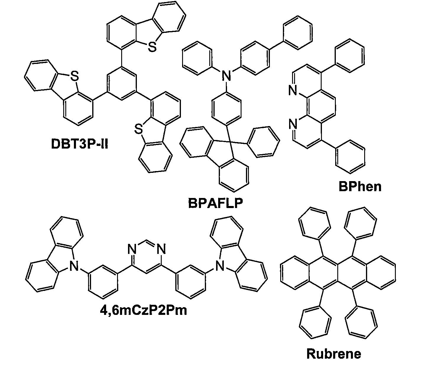

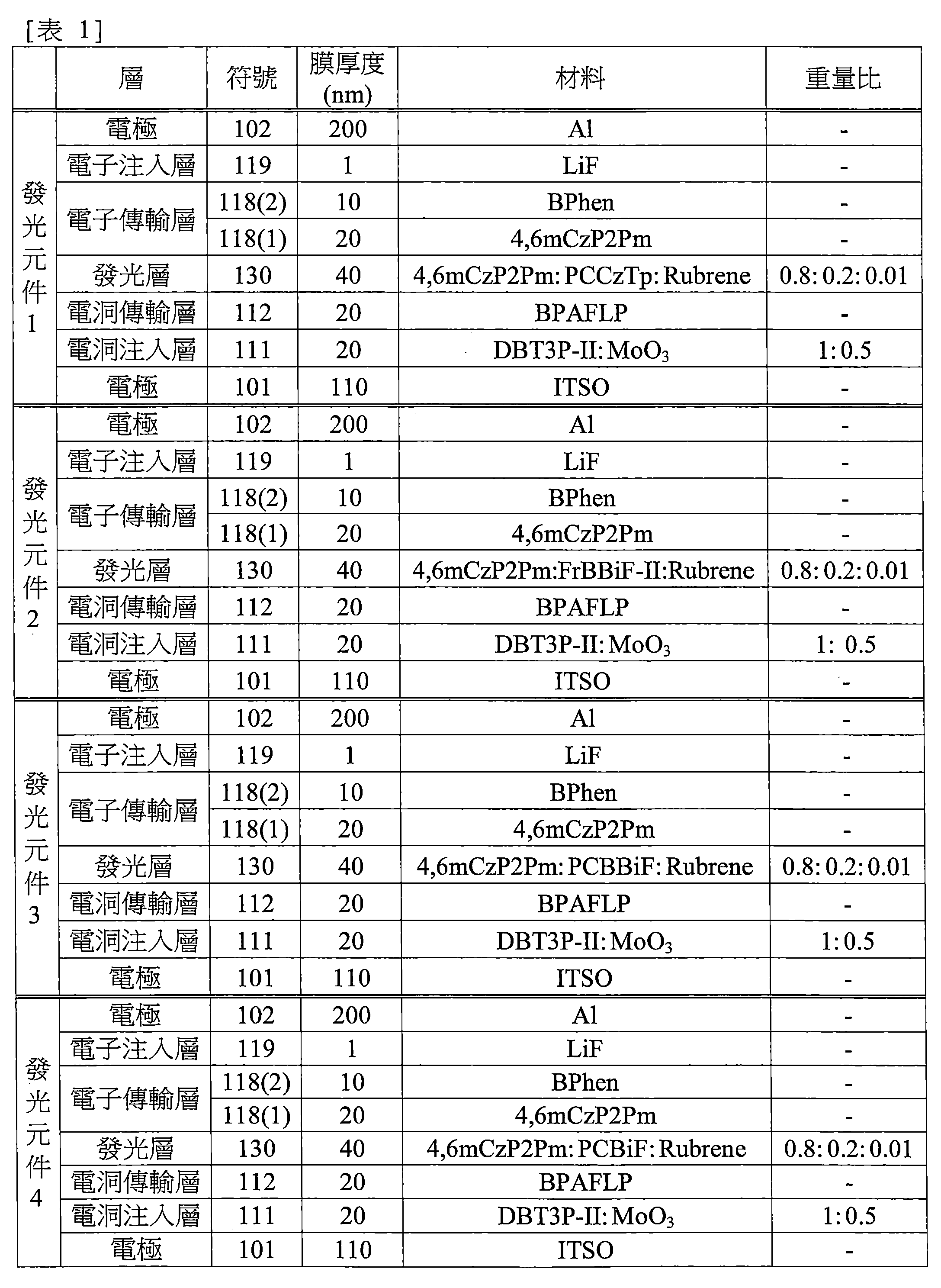
〈發光元件1的製造〉
<Manufacturing of light-emitting
作為電極101,在基板上形成厚度為110nm的ITSO膜。電極101的面積為4mm2(2mm×2mm)。
An ITSO film having a thickness of 110 nm was formed on a substrate as the
接著,在電極101上形成EL層100。作為電洞注入層111,以1,3,5-三(二苯并噻吩-4-基)苯(簡稱:DBT3P-II)與氧化鉬(MoO3)的重量比(DBT3P-II:MoO3)為1:0.5的方式共蒸鍍以形成厚度為20nm的電洞注入層111。另外,作為電洞傳輸層112,以厚度為20nm的方式蒸鍍4-苯基-4’-(9-苯基茀-9-基)三苯胺(簡稱:BPAFLP)。
Next, the
接著,作為發光層130,以4,6-雙[3-(9H-咔唑-9-基)苯基]嘧啶(簡稱:4,6mCzP2Pm)、9-苯基-9’-(聯伸三苯-2-基)-3,3’-聯-9H-咔唑(簡稱:PCCzTp)、紅螢烯(也稱為Rubrene)的重量比(4,6mCzP2Pm:PCCzTp:Rubrene)為0.8:0.2:0.01的方式共蒸鍍以形成厚度為40nm的發光層130。注意,在發光層130中,4,6mCzP2Pm及PCCzTp是主體材料131,Rubrene是客體材料132(螢光材料)。
Next, as the light-emitting
另外,作為電子傳輸層118,在發光層130上依次以厚度為20nm的方式蒸鍍4,6mCzP2Pm並且以厚度為10nm的方式蒸鍍BPhen。接著,作為電子注入層119,以厚度為1nm的方式蒸鍍氟化鋰(LiF)。
In addition, as the
另外,作為電極102,形成厚度為200nm的
鋁(Al)。
In addition, as the
接著,在氮氛圍的手套箱中使用有機EL用密封材料將密封基板固定於形成有EL層100的基板上,由此密封發光元件1。明確而言,將密封材料塗佈於形成在基板上的EL層100的周圍,貼合該基板和密封基板,以6J/cm2照射波長為365nm的紫外光,並且以80℃進行1小時的加熱處理。藉由上述製程得到發光元件1。
Next, in a glove box in a nitrogen atmosphere, a sealing substrate is fixed to the substrate on which the
〈發光元件2至發光元件4的製造〉
<Manufacturing of light-emitting
發光元件2至發光元件4與上述發光元件1的不同之處僅在於發光層130的主體材料,而其他製程都與發光元件1採用同樣的製造方法。
The only difference between light-emitting
作為發光元件2的發光層130,以4,6mCzP2Pm、N-(1,1’-聯苯-4-基)-N-[4-(二苯并呋喃-4-基)苯基]-9,9-二甲基-9H-茀-2-胺(簡稱:FrBBiF-II)、Rubrene的重量比(4,6mCzP2Pm:FrBBiF-II:Rubrene)為0.8:0.2:0.01的方式共蒸鍍以形成厚度為40nm的發光層130。注意,在發光層130中,4,6mCzP2Pm及FrBBiF-II是主體材料131,Rubrene是客體材料132(螢光材料)。
As the light-emitting
作為發光元件3的發光層130,以4,6mCzP2Pm、N-(1,1’-聯苯-4-基)-N-[4-(9-苯基-9H-咔唑-3-基)苯基]-9,9-二甲基-9H-茀-2-胺(簡稱:PCBBiF)、Rubrene的重量比(4,6mCzP2Pm:PCBBiF:Rubrene)為0.8:0.2:0.01的方式共蒸鍍以形成厚度為40nm的發光層
130。注意,在發光層130中,4,6mCzP2Pm及PCBBiF是主體材料131,Rubrene是客體材料132(螢光材料)。
As the light-emitting
作為發光元件4的發光層130,以4,6mCzP2Pm、N-(4-聯苯)-N-(9,9-二甲基-9H-茀-2-基)-9-苯基-9H-咔唑-3-胺(簡稱:PCBiF)、Rubrene的重量比(4,6mCzP2Pm:PCBiF:Rubrene)為0.8:0.2:0.01的方式共蒸鍍以形成厚度為40nm的發光層130。注意,在發光層130中,4,6mCzP2Pm及PCBiF是主體材料131,Rubrene是客體材料132(螢光材料)。
As the light-emitting
〈發光元件的工作特性1〉
<Operating characteristics of light-emitting
接著,對所製造的發光元件1至發光元件4的發光特性進行測定。注意,測定在室溫(保持為23℃的氛圍)中進行。
Next, the luminescent properties of the manufactured
在此,表2示出1000cd/m2附近的發光元件的發光特性。另外,圖29示出發光元件的電流效率-亮度特性,圖30示出外部量子效率-亮度特性,圖31示出亮度-電壓特性。圖32示出使電流密度為2.5mA/cm2的電流流過發光元件時的電致發射光譜。 Here, Table 2 shows the luminescence characteristics of the luminescent element near 1000 cd/m 2. In addition, FIG. 29 shows the current efficiency-luminance characteristics of the luminescent element, FIG. 30 shows the external quantum efficiency-luminance characteristics, and FIG. 31 shows the luminance-voltage characteristics. FIG. 32 shows the electroluminescence spectrum when a current density of 2.5 mA/cm 2 is passed through the luminescent element.

如圖32所示,從發光元件1至發光元件4的電致發射光譜的峰值僅觀察到作為螢光材料的Rubrene所呈現的黃色發光。
As shown in FIG32, the peak of the electroluminescence spectrum from light-emitting
另外,如圖29、圖30及表2所示,得出了發光元件1至發光元件4具有高電流效率及高外部量子效率的結果。另外,尤其是發光元件4,得出了其在1000cd/m2附近具有高於8%的外部量子效率的結果。
29, 30 and Table 2, it was found that light emitting
因從一對電極注入的載子(電洞及電子)的再結合而生成的單重態激子的最大生成概率為25%,因此,當光的外部提取效率為20%時,最大外部量子效率為5%。發光元件1至發光元件4可以具有高於5%的外部量子效率。這是因為:在發光元件1至發光元件4中,除了因從一對電極注入的載子(電洞及電子)的再結合而生成
的單重態激子所引起的發光以外,還可以得到藉由ExEF從三重態激子生成的單重態激子所引起的發光。
The maximum generation probability of singlet excitons generated by the recombination of carriers (holes and electrons) injected from a pair of electrodes is 25%, so when the external light extraction efficiency is 20%, the maximum external quantum efficiency is 5%. Light-emitting
另外,如圖31及表2所示,發光元件1至發光元件4是以低電壓驅動的。也就是說,可知,由於具有使用ExEF的發光層,可以製造以低電壓驅動的發光元件。另外,可知可以製造功耗得到降低的發光元件。
In addition, as shown in FIG. 31 and Table 2, light-emitting
接著,為調查發光元件1至發光元件4是否藉由ExEF發光,製造不包含客體材料132的發光元件且進行測定。表3示出元件的詳細結構。
Next, in order to investigate whether light-emitting
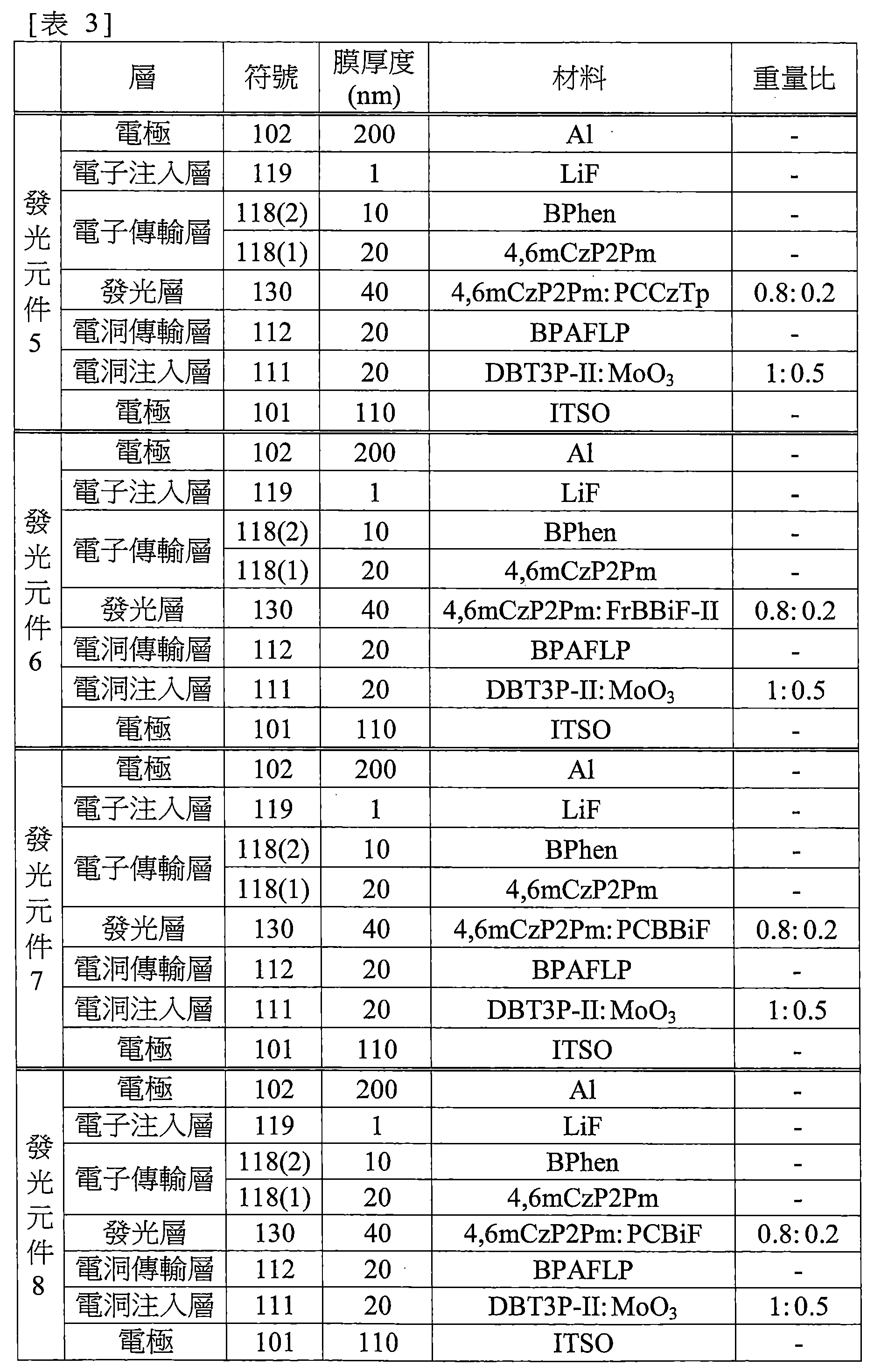
〈發光元件5至發光元件8的製造〉
<Manufacturing of light-emitting
發光元件5至發光元件8與上述發光元件1至發光元件4的不同之處僅分別在於發光元件5至發光元件8不包含發光層130的客體材料132,而其他製程都與發光元件1至發光元件4採用同樣的製造方法。
The only difference between the light-emitting
作為發光元件5的發光層130,以4,6mCzP2Pm與PCCzTp的重量比(4,6mCzP2Pm:PCCzTp)為0.8:0.2的方式共蒸鍍以形成厚度為40nm的發光層130。注意,在發光層130中,4,6mCzP2Pm及PCCzTp是主體材料131,不包含客體材料132。
As the light-emitting
作為發光元件6的發光層130,以4,6mCzP2Pm與FrBBiF-II的重量比(4,6mCzP2Pm:FrBBiF-II)為0.8:0.2的方式共蒸鍍以形成厚度為40nm的發光層130。注意,在發光層130中,4,6mCzP2Pm及FrBBiF-II是主體材料131,不包含客體材料132。
As the light-emitting
作為發光元件7的發光層130,以4,6mCzP2Pm與PCBBiF的重量比(4,6mCzP2Pm:PCBBiF)為0.8:0.2的方式共蒸鍍以形成厚度為40nm的發光層130。注意,在發光層130中,4,6mCzP2Pm及PCBBiF是主體材料131,不包含客體材料132。
As the light-emitting
作為發光元件8的發光層130,以4,6mCzP2Pm與PCBiF的重量比(4,6mCzP2Pm:PCBiF)為0.8:0.2的方式共蒸鍍以形成厚度為40nm的發光層130。注意,
在發光層130中,4,6mCzP2Pm及PCBiF是主體材料131,不包含客體材料132。
As the light-emitting
〈發光元件的工作特性2〉
<Operating characteristics of light-emitting
接著,對所製造的發光元件5至發光元件8的發光特性進行測定。注意,測定在室溫(保持為23℃的氛圍)中進行。
Next, the luminescent properties of the manufactured
在此,表4示出1000cd/m2附近的發光元件的發光特性。另外,圖33示出發光元件的電流效率-亮度特性,圖34示出外部量子效率-亮度特性,圖35示出亮度-電壓特性。圖36示出使電流密度為2.5mA/cm2的電流流過發光元件時的電致發射光譜。 Here, Table 4 shows the luminescence characteristics of the luminescent element near 1000 cd/m 2. In addition, FIG33 shows the current efficiency-luminance characteristics of the luminescent element, FIG34 shows the external quantum efficiency-luminance characteristics, and FIG35 shows the luminance-voltage characteristics. FIG36 shows the electroluminescence spectrum when a current density of 2.5 mA/cm 2 is passed through the luminescent element.

另外,圖37分別示出用作主體材料的4,6mCzP2Pm、PCCzTp、FrBBiF-II、PCBBiF及PCBiF的薄膜的發射光譜。注意,在測定薄膜的發射光譜時,使用PL-EL測定裝置(日本濱松光子學公司製造)。 In addition, FIG. 37 shows the emission spectra of thin films of 4,6mCzP2Pm, PCCzTp, FrBBiF-II, PCBBiF, and PCBiF used as host materials, respectively. Note that a PL-EL measuring device (manufactured by Hamamatsu Photonics Co., Ltd., Japan) was used when measuring the emission spectra of the thin films.
如圖37所示,從用作主體材料的4,6mCzP2Pm、PCCzTp、FrBBiF-II、PCBBiF及PCBiF觀察到峰值波長分別為493nm、418nm、428nm、436nm及430nm的藍色發光。 As shown in FIG37 , blue luminescence with peak wavelengths of 493 nm, 418 nm, 428 nm, 436 nm, and 430 nm was observed from 4,6mCzP2Pm, PCCzTp, FrBBiF-II, PCBBiF, and PCBiF used as host materials, respectively.
另一方面,如圖36所示,從發光元件5、發光元件6、發光元件7及發光元件8的電致發射光譜的峰值觀察到峰值波長分別為499nm、513nm、536nm及552nm的綠色至黃色的發光,發射光譜的半峰全寬(FWHM:full width at half maximum)都比化合物單獨的發射光譜大。發光元件5至發光元件8的發射光譜的波長分別與4,6mCzP2Pm的LUMO能階和PCCzTp的HOMO能階的能量差、4,6mCzP2Pm的LUMO能階和FrBBiF-II的HOMO能階的能量差、4,6mCzP2Pm的LUMO能階和PCBBiF的HOMO能階的能量差、4,6mCzP2Pm的LUMO能階和PCBiF的HOMO能階的能量差有關聯,因此可以說發光是4,6mCzP2Pm和PCCzTp的激態錯合物、4,6mCzP2Pm和FrBBiF-II的激態錯合物、4,6mCzP2Pm和PCBBiF的激態錯合物、4,6mCzP2Pm和PCBiF的激態錯合物呈現的發光。
On the other hand, as shown in FIG36, green to yellow luminescence with peak wavelengths of 499 nm, 513 nm, 536 nm, and 552 nm was observed from the peaks of the electroluminescence spectra of light-emitting
另外,圖38示出含有用作發光元件1至發光
元件4的客體材料的Rubrene的甲苯溶液的吸收光譜的測定結果。
In addition, FIG. 38 shows the measurement results of the absorption spectrum of a toluene solution containing Rubrene used as the guest material of light-emitting
如圖38所示,Rubrene的吸收光譜在450nm至550nm附近呈現具有高莫耳吸光係數的吸收帶。該結果與圖36所示的激態錯合物的電致發射光譜的波長範圍大致一致。由此可知,藉由作為發光元件1至發光元件4的主體材料使用形成激態錯合物的組合的化合物,對客體材料的能量轉移效率變高,所以是較佳的。
As shown in FIG38, the absorption spectrum of Rubrene shows an absorption band with a high molar absorption coefficient near 450nm to 550nm. This result is roughly consistent with the wavelength range of the electroluminescence spectrum of the excited state complex shown in FIG36. It can be seen that by using a compound that forms a combination of excited state complexes as the host material of light-emitting
另外,如圖33、圖34及表4所示,得出了發光元件7及發光元件8具有高發光效率(電流效率及外部量子效率)的結果。另外,尤其是發光元件8,得出了即使在高亮度一側,其發光效率的降低(衰減(roll-off))也小的結果。
In addition, as shown in Figures 33, 34 and Table 4, it was found that light-emitting element 7 and light-emitting
可知:在1000cd/m2附近,發光元件5與發光元件6的發光效率大致一致,發光元件7的發光效率高於發光元件5及發光元件6,發光元件8的發光效率高於發光元件7。另外,可知:在上述發光元件1至發光元件4中,在1000cd/m2附近,發光元件1與發光元件2的發光效率大致一致,發光元件3的發光效率高於發光元件1及發光元件2,發光元件4的發光效率高於發光元件3。
It can be seen that: in the vicinity of 1000 cd/m 2 , the luminous efficiency of light-emitting
也就是說,可知激態錯合物所呈現的發光的發光效率與客體材料所呈現的發光的發光效率有關聯。激態錯合物的發光效率高意味著激態錯合物中的無輻射失活 的速度常數小,這表示反系間跨越的速度常數大。 In other words, it can be seen that the luminescence efficiency of the luminescence presented by the excited state complex is related to the luminescence efficiency of the luminescence presented by the guest material. The high luminescence efficiency of the excited state complex means that the rate constant of the non-radiative deactivation in the excited state complex is small, which means that the rate constant of the antisystem crossing is large.
於是,接著,對與發光元件5至發光元件8的發光層同樣的薄膜進行時間分辨螢光測定(time-resolved fluorescence measurement)。
Then, time-resolved fluorescence measurement was performed on the same thin film as the light-emitting layer of light-emitting
〈薄膜樣本的製造〉 〈Manufacturing of thin film samples〉
為進行發光元件的發光層的時間分辨螢光測定,在石英基板上利用真空蒸鍍法製造薄膜樣本。 In order to perform time-resolved fluorescence measurement of the light-emitting layer of the light-emitting element, a thin film sample was produced on a quartz substrate using vacuum evaporation.
作為薄膜1,以4,6mCzP2Pm與FrBBiF-II的重量比(4,6mCzP2Pm:FrBBiF-II)為0.8:0.2的方式共蒸鍍以形成厚度為50nm的薄膜1。
As the
作為薄膜2,以4,6mCzP2Pm與PCBBiF的重量比(4,6mCzP2Pm:PCBBiF)為0.8:0.2的方式共蒸鍍以形成厚度為50nm的薄膜2。
As the
作為薄膜3,以4,6mCzP2Pm與PCBiF的重量比(4,6mCzP2Pm:PCBiF)為0.8:0.2的方式共蒸鍍以形成厚度為50nm的薄膜3。
As the
另外,在氮氛圍的手套箱中使用有機EL用密封材料將密封基板固定於形成有薄膜樣本的石英基板上,由此密封薄膜1至薄膜3。明確而言,將密封材料塗佈於形成在石英基板上的薄膜的周圍,貼合該石英基板和密封基板,以6J/cm2照射波長為365nm的紫外光,並且以80℃進行1小時的加熱處理。
In addition, a sealing substrate was fixed to the quartz substrate on which the thin film sample was formed using a sealing material for organic EL in a glove box in a nitrogen atmosphere, thereby sealing
〈薄膜樣本的時間分辨螢光測定〉 〈Time-resolved fluorescence measurement of thin film samples〉
在測定中,使用皮秒螢光壽命測定系統(日本濱松光子學公司製造)。在本測定中,為了測定薄膜所呈現的螢光發光的壽命,對薄膜照射脈衝雷射,並且使用條紋相機對在照射雷射之後衰減的發光進行時間分辨測定。作為脈衝雷射使用波長為337nm的氮氣體雷射,以10Hz的頻率對薄膜照射500ps的脈衝雷射,並且藉由將反復測量的資料累計起來獲得S/N比例高的資料。注意,測定在室溫(保持為23℃的氛圍)中進行。 In the measurement, a picosecond fluorescence lifetime measurement system (manufactured by Hamamatsu Photonics Co., Ltd., Japan) was used. In this measurement, in order to measure the lifetime of the fluorescent luminescence exhibited by the thin film, the thin film was irradiated with a pulse laser, and the luminescence decaying after the laser irradiation was time-resolved and measured using a stripe camera. A nitrogen gas laser with a wavelength of 337nm was used as a pulse laser, and a pulse laser of 500ps was irradiated to the thin film at a frequency of 10Hz, and data with a high S/N ratio was obtained by accumulating the data of repeated measurements. Note that the measurement was performed at room temperature (an atmosphere maintained at 23°C).
從薄膜1至薄膜3分別觀察到由兩個化合物形成的激態錯合物所呈現的發光。圖39A及圖39B示出由測定而得的衰減曲線。
Luminescence from excited complexes formed by two compounds was observed from
另外,使用下述公式4對圖39A及圖39B所示的衰減曲線進行擬合。
In addition, the attenuation curves shown in Figures 39A and 39B are fitted using the following

在公式4中,L表示正規化的發光強度,t表示經過時間。當n為1及2時,可以對衰減曲線進行擬合。由衰減曲線的擬合結果可知,薄膜1的發光成分包含螢光壽命為0.60μs的瞬時螢光成分(包括prompt成分)以及螢光壽命為96μs的延遲螢光成分(也稱為delayed成分)。另外,可知薄膜2的發光成分包含螢光壽命為
0.72μs的瞬時螢光成分以及螢光壽命為55μs的延遲螢光成分。另外,可知薄膜3的發光成分包含螢光壽命為0.67μs的瞬時螢光成分以及螢光壽命為23μs的延遲螢光成分。也就是說,在得到高發光效率的發光元件4及發光元件8中使用的激態錯合物的延遲螢光壽命比在其他的發光元件2、發光元件3、發光元件6及發光元件7中使用的激態錯合物的延遲螢光壽命短,亦即為50μs以下。另外,薄膜1至薄膜3中的該延遲螢光成分在發光中所占的比率分別為0.084%、3.8%、9.4%。
In
如上所述,可知薄膜3包含螢光壽命較短的延遲螢光成分。延遲螢光成分的壽命短意味著反系間跨越的速度常數大,因此所得到的結果進一步證實了由發光元件8的測定而得到的結果。也就是說,由於激態錯合物的三重態激子以較短的時間被轉換為單重態激子,即使在高亮度區域(激子密度高的區域)也沒有發生激子密度的飽和,因此,可以說得出了發光元件8在高亮度區域不容易發生發光效率的降低的結果。另外,當對發光元件1至發光元件4進行比較時,雖然發光元件3(在時間分辨螢光測定中激態錯合物的延遲螢光壽命為55μs)的發光效率也比發光元件1及發光元件2高,但是發光效率的增高更加顯著的是發光元件4(在時間分辨螢光測定中激態錯合物的延遲螢光壽命為23μs)。也就是說,在本發明的一個實施方式中,時間分辨螢光測定中的激態錯合物的延遲螢光壽命較佳為50μs以下,更佳為40μs以下,進一步較
佳為30μs以下。
As described above, it is known that the thin film 3 contains a delayed fluorescence component with a short fluorescence lifetime. The short lifetime of the delayed fluorescence component means that the rate constant of the antisystem crossing is large, so the obtained result further confirms the result obtained by the measurement of the light-emitting
另外,在時間分辨螢光測定中,薄膜3所呈現的發光包含5%以上的延遲螢光成分,由此可知單重激發態與三重激發態的能量轉移的發生概率較高。 In addition, in the time-resolved fluorescence measurement, the luminescence presented by the film 3 contains more than 5% of the delayed fluorescence component, which shows that the probability of energy transfer between the singlet excited state and the triplet excited state is higher.
另外,作為主體材料包含壽命短的延遲螢光成分的激態錯合物的發光元件4得到示出高發光效率的結果。這是因為:由於激態錯合物的三重態激子以短時間被轉換為單重態激子,所以從激態錯合物的三重激發態到客體材料的三重激發態的能量轉移效率降低,從而實現了激態錯合物及客體材料中的單重態激子的生成效率的增高。
In addition, the light-emitting
如上所示,可知:藉由作為主體材料包含形成激態錯合物的化合物,並且該激態錯合物包含5%以上的螢光壽命較短(亦即為50μs以下)的延遲螢光成分,可以製造具有如發光元件4所示那樣的高發光效率的發光元件。
As shown above, it can be seen that: by including a compound that forms an excited state complex as a host material, and the excited state complex contains more than 5% of a delayed fluorescence component with a short fluorescence lifetime (i.e., less than 50μs), a light-emitting element with high light-emitting efficiency as shown in light-emitting
本實施例所示的結構可以與其他實施方式所示的結構適當地組合而使用。 The structure shown in this embodiment can be used in combination with the structures shown in other embodiments as appropriate.
131_1:有機化合物 131_1: Organic compounds
131_2:有機化合物 131_2: Organic compounds
132:客體材料 132:Objective material
E3、E4、E5、E6:路徑 E 3 , E 4 , E 5 , E 6 : path
SH、SE、SG:單重激發能階 S H , S E , S G : Singlet excitation energy levels
TE、TG:三重激發能階 TE , TG : triple excitation energy level
Claims (8)


Applications Claiming Priority (2)
| Application Number | Priority Date | Filing Date | Title |
|---|---|---|---|
| JP2015-046376 | 2015-03-09 | ||
| JP2015046376 | 2015-03-09 |
Publications (2)
| Publication Number | Publication Date |
|---|---|
| TW202404148A TW202404148A (en) | 2024-01-16 |
| TWI860824B true TWI860824B (en) | 2024-11-01 |
Family
ID=56888261
Family Applications (4)
| Application Number | Title | Priority Date | Filing Date |
|---|---|---|---|
| TW112132418A TWI860824B (en) | 2015-03-09 | 2016-03-04 | Light-emitting element, display device, electronic device, and lighting device |
| TW105106744A TWI704706B (en) | 2015-03-09 | 2016-03-04 | Light-emitting element, display device, electronic device, and lighting device |
| TW109128649A TWI749726B (en) | 2015-03-09 | 2016-03-04 | Light-emitting element, display device, electronic device, and lighting device |
| TW110143588A TWI814143B (en) | 2015-03-09 | 2016-03-04 | Light-emitting element, display device, electronic device, and lighting device |
Family Applications After (3)
| Application Number | Title | Priority Date | Filing Date |
|---|---|---|---|
| TW105106744A TWI704706B (en) | 2015-03-09 | 2016-03-04 | Light-emitting element, display device, electronic device, and lighting device |
| TW109128649A TWI749726B (en) | 2015-03-09 | 2016-03-04 | Light-emitting element, display device, electronic device, and lighting device |
| TW110143588A TWI814143B (en) | 2015-03-09 | 2016-03-04 | Light-emitting element, display device, electronic device, and lighting device |
Country Status (5)
| Country | Link |
|---|---|
| US (4) | US9954177B2 (en) |
| JP (4) | JP2016171319A (en) |
| KR (3) | KR102567176B1 (en) |
| CN (2) | CN111916568B (en) |
| TW (4) | TWI860824B (en) |
Families Citing this family (41)
| Publication number | Priority date | Publication date | Assignee | Title |
|---|---|---|---|---|
| JP6312960B2 (en) * | 2012-08-03 | 2018-04-18 | 株式会社半導体エネルギー研究所 | Light emitting element, light emitting device, electronic device, lighting device, and heterocyclic compound |
| TWI860824B (en) | 2015-03-09 | 2024-11-01 | 日商半導體能源研究所股份有限公司 | Light-emitting element, display device, electronic device, and lighting device |
| TWI737594B (en) * | 2015-03-09 | 2021-09-01 | 日商半導體能源研究所股份有限公司 | Light-emitting element, display device, electronic device, and lighting device |
| CN104966789A (en) * | 2015-06-30 | 2015-10-07 | 深圳市华星光电技术有限公司 | Charge coupling layer, manufacturing method thereof and stacked OLED device |
| KR102490381B1 (en) * | 2015-12-24 | 2023-01-18 | 엘지디스플레이 주식회사 | Organic light emitting display device and organic light emitting stacked structure |
| CN105789237A (en) * | 2016-04-25 | 2016-07-20 | 京东方科技集团股份有限公司 | LED display module, LED display device and manufacturing method of LED display module |
| WO2017191526A1 (en) | 2016-05-06 | 2017-11-09 | Semiconductor Energy Laboratory Co., Ltd. | Light-emitting element, display device, electronic device, and lighting device |
| CN106229423B (en) * | 2016-07-01 | 2018-07-17 | 京东方科技集团股份有限公司 | Quanta point electroluminescent device, preparation method and display device |
| WO2018062277A1 (en) * | 2016-09-29 | 2018-04-05 | 住友化学株式会社 | Light-emitting element |
| CN108336237B (en) | 2017-01-20 | 2020-01-31 | 昆山工研院新型平板显示技术中心有限公司 | An organic electroluminescent device |
| CN107329319A (en) * | 2017-07-21 | 2017-11-07 | 苏州星烁纳米科技有限公司 | Quantum dot diaphragm and preparation method thereof, backlight module |
| CN108346750B (en) * | 2017-08-08 | 2019-07-19 | 广东聚华印刷显示技术有限公司 | Electroluminescent device and its luminescent layer and application |
| CN119894227A (en) | 2017-11-02 | 2025-04-25 | 株式会社半导体能源研究所 | Light emitting element, display device, electronic device, and lighting device |
| KR102408906B1 (en) * | 2017-11-30 | 2022-06-15 | 엘지디스플레이 주식회사 | Organic Light Emitting Device And Organic Light Emitting Display Device Using the Same |
| CN108963089A (en) * | 2017-12-19 | 2018-12-07 | 广东聚华印刷显示技术有限公司 | Quanta point electroluminescent device |
| WO2019123190A1 (en) * | 2017-12-22 | 2019-06-27 | 株式会社半導体エネルギー研究所 | Light-emitting element, light-emitting device, electronic equipment, and illumination device |
| CN109994634B (en) | 2017-12-29 | 2020-12-11 | 昆山国显光电有限公司 | Organic Electroluminescent Devices |
| CN108365112B (en) * | 2018-01-19 | 2020-06-16 | 昆山国显光电有限公司 | Electroluminescent device |
| KR20250151571A (en) | 2018-03-07 | 2025-10-21 | 가부시키가이샤 한도오따이 에네루기 켄큐쇼 | Light emitting element, display device, electronic device, organic compound, and lighting device |
| CN109713143A (en) * | 2018-03-19 | 2019-05-03 | 广东聚华印刷显示技术有限公司 | Electroluminescent device, display device and preparation method thereof |
| CN109705667A (en) * | 2018-03-19 | 2019-05-03 | 广东聚华印刷显示技术有限公司 | Quantum dot ink and preparation method thereof |
| CN112189265B (en) * | 2018-05-11 | 2025-02-14 | 株式会社半导体能源研究所 | Light-emitting element, display device, electronic device, organic compound, and lighting device |
| CN112119445B (en) * | 2018-05-17 | 2024-10-15 | 株式会社半导体能源研究所 | Display device |
| CN109144311B (en) * | 2018-07-26 | 2022-06-07 | 京东方科技集团股份有限公司 | Display substrate, fingerprint identification method, and touch display device |
| CN109346614B (en) * | 2018-08-31 | 2020-01-31 | 昆山国显光电有限公司 | organic electroluminescent device and display device |
| CN112639937B (en) | 2018-09-05 | 2023-06-23 | 株式会社半导体能源研究所 | Display device, display module, electronic device and method for manufacturing display device |
| KR20250024132A (en) | 2018-09-07 | 2025-02-18 | 가부시키가이샤 한도오따이 에네루기 켄큐쇼 | Display device, display module, and electronic device |
| WO2020065472A1 (en) | 2018-09-28 | 2020-04-02 | 株式会社半導体エネルギー研究所 | Method for manufacturing display device, and device for manufacturing display device |
| WO2020111251A1 (en) | 2018-11-30 | 2020-06-04 | 出光興産株式会社 | Compound, material for organic electroluminescent element, organic electroluminescent element, and electronic device |
| JP7341172B2 (en) | 2019-02-06 | 2023-09-08 | 株式会社半導体エネルギー研究所 | Light emitting devices, electronic equipment and lighting equipment |
| JPWO2020217129A1 (en) | 2019-04-25 | 2020-10-29 | ||
| US12048242B2 (en) | 2019-05-31 | 2024-07-23 | Idemitsu Kosan Co., Ltd. | Compound, material for organic electroluminescent elements, organic electroluminescent element, and electronic device |
| JP7538132B2 (en) | 2019-09-06 | 2024-08-21 | 株式会社半導体エネルギー研究所 | Organic compounds, materials for light-emitting devices, light-emitting devices, light-emitting devices, electronic devices and lighting devices |
| CN111883676A (en) * | 2019-09-24 | 2020-11-03 | 广东聚华印刷显示技术有限公司 | Electroluminescent device and display device |
| CN111883678A (en) * | 2019-09-24 | 2020-11-03 | 广东聚华印刷显示技术有限公司 | Electroluminescent device and display device |
| JP7641724B2 (en) | 2019-11-12 | 2025-03-07 | 株式会社半導体エネルギー研究所 | Functional panel, display device, input/output device, information processing device |
| US11610877B2 (en) | 2019-11-21 | 2023-03-21 | Semiconductor Energy Laboratory Co., Ltd. | Functional panel, display device, input/output device, and data processing device |
| KR102848957B1 (en) | 2019-11-26 | 2025-08-20 | 삼성전자주식회사 | Semiconductor light emitting device and method of fabricating the same |
| CN110911575B (en) * | 2019-11-29 | 2023-04-07 | 昆山国显光电有限公司 | Organic electroluminescent device and display device |
| CN111916574B (en) * | 2020-08-21 | 2023-12-01 | 京东方科技集团股份有限公司 | Blue light electroluminescent device, display panel and display device |
| EP4625399A3 (en) | 2021-04-01 | 2025-11-12 | BOE Technology Group Co., Ltd. | Light-emitting substrate |
Citations (3)
| Publication number | Priority date | Publication date | Assignee | Title |
|---|---|---|---|---|
| JP2014045179A (en) * | 2012-08-03 | 2014-03-13 | Semiconductor Energy Lab Co Ltd | Light emitting element |
| TW201434832A (en) * | 2013-02-12 | 2014-09-16 | Univ Kyushu Nat Univ Corp | Compound, light-emitting material and organic electroluminescence device |
| JP2014192214A (en) * | 2013-03-26 | 2014-10-06 | Semiconductor Energy Lab Co Ltd | Light-emitting element, light-emitting device, display device, electronic apparatus and light device |
Family Cites Families (115)
| Publication number | Priority date | Publication date | Assignee | Title |
|---|---|---|---|---|
| JPH0785972A (en) | 1993-09-20 | 1995-03-31 | Toshiba Corp | Organic EL element |
| WO2000070655A2 (en) | 1999-05-13 | 2000-11-23 | The Trustees Of Princeton University | Very high efficiency organic light emitting devices based on electrophosphorescence |
| EP1202608B2 (en) | 2000-10-30 | 2012-02-08 | Kabushiki Kaisha Toyota Chuo Kenkyusho | Organic light-emitting devices |
| SG138466A1 (en) | 2000-12-28 | 2008-01-28 | Semiconductor Energy Lab | Luminescent device |
| TW519770B (en) | 2001-01-18 | 2003-02-01 | Semiconductor Energy Lab | Light emitting device and manufacturing method thereof |
| CN1553938B (en) * | 2001-06-29 | 2010-11-03 | 西巴特殊化学品控股有限公司 | Fluorescent diketopyrrolopyrroles |
| ITTO20010692A1 (en) | 2001-07-13 | 2003-01-13 | Consiglio Nazionale Ricerche | ORGANIC ELECTROLUMINESCENT DEVICE BASED ON THE EMISSION OF EXCIPLEXES OR ELECTROPLLEXES AND ITS REALIZATION. |
| US6863997B2 (en) | 2001-12-28 | 2005-03-08 | The Trustees Of Princeton University | White light emitting OLEDs from combined monomer and aggregate emission |
| ITBO20020165A1 (en) | 2002-03-29 | 2003-09-29 | Consiglio Nazionale Ricerche | ORGANIC ELECTROLUMINESCENT DEVICE WITH CHROMOPHOR DROGANTS |
| TWI314947B (en) | 2002-04-24 | 2009-09-21 | Eastman Kodak Compan | Organic light emitting diode devices with improved operational stability |
| JP2004241374A (en) | 2003-01-17 | 2004-08-26 | Sogo Pharmaceutical Co Ltd | Organic electroluminescent element |
| TWI316827B (en) | 2003-02-27 | 2009-11-01 | Toyota Jidoshokki Kk | Organic electroluminescent device |
| JP4531342B2 (en) | 2003-03-17 | 2010-08-25 | 株式会社半導体エネルギー研究所 | White organic light emitting device and light emitting device |
| US7175922B2 (en) | 2003-10-22 | 2007-02-13 | Eastman Kodak Company | Aggregate organic light emitting diode devices with improved operational stability |
| JP2006024830A (en) | 2004-07-09 | 2006-01-26 | Sogo Pharmaceutical Co Ltd | Organic electroluminescent device |
| US7597967B2 (en) | 2004-12-17 | 2009-10-06 | Eastman Kodak Company | Phosphorescent OLEDs with exciton blocking layer |
| US20060134464A1 (en) | 2004-12-22 | 2006-06-22 | Fuji Photo Film Co. Ltd | Organic electroluminescent element |
| JP4559922B2 (en) * | 2005-06-21 | 2010-10-13 | 株式会社東芝 | Fluorescent complex and lighting device using the same |
| US20070090756A1 (en) | 2005-10-11 | 2007-04-26 | Fujifilm Corporation | Organic electroluminescent element |
| EP1956022B1 (en) | 2005-12-01 | 2012-07-25 | Nippon Steel Chemical Co., Ltd. | Compound for organic electroluminescent element and organic electroluminescent element |
| CN101321773B (en) | 2005-12-05 | 2015-02-25 | 株式会社半导体能源研究所 | Organometallic complex and light-emitting element, light-emitting device and electronic device using the same |
| EP2254173B1 (en) | 2006-03-21 | 2013-09-18 | Semiconductor Energy Laboratory Co, Ltd. | Organometallic complex and light emitting element, light emitting device, and electronic device using the organometallic complex |
| JP5238227B2 (en) | 2006-12-27 | 2013-07-17 | 株式会社半導体エネルギー研究所 | ORGANIC METAL COMPLEX AND LIGHT EMITTING ELEMENT, LIGHT EMITTING DEVICE, AND ELECTRONIC DEVICE |
| EP1973386B8 (en) * | 2007-03-23 | 2016-01-13 | Semiconductor Energy Laboratory Co., Ltd. | Light-emitting device and electronic device |
| JP2008288344A (en) | 2007-05-16 | 2008-11-27 | Nippon Hoso Kyokai <Nhk> | Organic EL device |
| CN101679467B (en) | 2007-05-18 | 2016-03-02 | 株式会社半导体能源研究所 | Organometallic complex, composition comprising the organometallic complex, and light-emitting element |
| US8034465B2 (en) | 2007-06-20 | 2011-10-11 | Global Oled Technology Llc | Phosphorescent oled having double exciton-blocking layers |
| US8080811B2 (en) | 2007-12-28 | 2011-12-20 | Semiconductor Energy Laboratory Co., Ltd. | Method for manufacturing evaporation donor substrate and light-emitting device |
| JP5325707B2 (en) | 2008-09-01 | 2013-10-23 | 株式会社半導体エネルギー研究所 | Light emitting element |
| WO2010026859A1 (en) | 2008-09-05 | 2010-03-11 | Semiconductor Energy Laboratory Co., Ltd. | Light-emitting element, light-emitting device, and electronic device |
| US8206842B2 (en) * | 2009-04-06 | 2012-06-26 | Global Oled Technology Llc | Organic element for electroluminescent devices |
| US8476823B2 (en) | 2009-05-22 | 2013-07-02 | Idemitsu Kosan Co., Ltd. | Organic electroluminescent device |
| WO2010148085A1 (en) * | 2009-06-16 | 2010-12-23 | The United States Of America, As Represented By The Secretary, Department Of Health And Human Services | Rna nanoparticles and methods of use |
| US8766269B2 (en) | 2009-07-02 | 2014-07-01 | Semiconductor Energy Laboratory Co., Ltd. | Light-emitting device, lighting device, and electronic device |
| JP5486440B2 (en) | 2009-08-27 | 2014-05-07 | 日本放送協会 | Organic EL elements, display devices, lighting equipment |
| JP2011088887A (en) | 2009-09-22 | 2011-05-06 | Semiconductor Energy Lab Co Ltd | Halogenated diarylamine compound and method for synthesizing the same |
| JP5732463B2 (en) | 2009-10-05 | 2015-06-10 | トルン ライティング リミテッドThorn Lighting Limited | Multi-layer organic element |
| KR101352116B1 (en) | 2009-11-24 | 2014-01-14 | 엘지디스플레이 주식회사 | White Organic Light Emitting Device |
| EP3176241A1 (en) | 2009-12-07 | 2017-06-07 | Nippon Steel & Sumikin Chemical Co., Ltd. | Organic light-emitting material and organic light-emitting element |
| EP2363398B1 (en) | 2010-03-01 | 2017-10-18 | Semiconductor Energy Laboratory Co., Ltd. | Heterocyclic compound, light-emitting element, light-emitting device, electronic device, and lighting device |
| EP2366753B1 (en) | 2010-03-02 | 2015-06-17 | Semiconductor Energy Laboratory Co., Ltd. | Light-Emitting Element and Lighting Device |
| JP2011213643A (en) | 2010-03-31 | 2011-10-27 | Canon Inc | Copper complex compound and organic luminescent element using the same |
| KR20110122051A (en) | 2010-05-03 | 2011-11-09 | 제일모직주식회사 | Compound for organic photoelectric device and organic photoelectric device comprising same |
| JP5602555B2 (en) | 2010-05-17 | 2014-10-08 | 株式会社半導体エネルギー研究所 | LIGHT EMITTING ELEMENT, LIGHT EMITTING DEVICE, ELECTRONIC DEVICE, AND LIGHTING DEVICE |
| JP5767237B2 (en) | 2010-10-13 | 2015-08-19 | 新日鉄住金化学株式会社 | Nitrogen-containing aromatic compounds, organic semiconductor materials, and organic electronic devices |
| KR102071726B1 (en) | 2010-10-22 | 2020-01-30 | 가부시키가이샤 한도오따이 에네루기 켄큐쇼 | Organometallic complex, light-emitting element, light-emitting device, electronic device and lighting device |
| KR101720444B1 (en) | 2011-02-07 | 2017-03-27 | 이데미쓰 고산 가부시키가이샤 | Biscarbazole derivative and organic electroluminescent element using same |
| TWI591154B (en) | 2011-02-07 | 2017-07-11 | Idemitsu Kosan Co | Biscarbazole derivatives and organic electroluminescent devices using the same |
| WO2012111680A1 (en) | 2011-02-16 | 2012-08-23 | Semiconductor Energy Laboratory Co., Ltd. | Light-emitting body, light-emitting layer, and light-emitting device |
| DE112012007377B4 (en) | 2011-02-16 | 2025-08-07 | Semiconductor Energy Laboratory Co., Ltd. | Light-emitting element |
| CN121442891A (en) * | 2011-02-16 | 2026-01-30 | 株式会社半导体能源研究所 | Light-emitting element |
| TW202542110A (en) | 2011-02-28 | 2025-11-01 | 日商半導體能源研究所股份有限公司 | Light-emitting element |
| US8969854B2 (en) | 2011-02-28 | 2015-03-03 | Semiconductor Energy Laboratory Co., Ltd. | Light-emitting layer and light-emitting element |
| KR101569599B1 (en) * | 2011-03-14 | 2015-11-16 | 아사히 가세이 케미칼즈 가부시키가이샤 | Organic/inorganic composite, manufacturing method therefor, organic/inorganic composite film, manufacturing method therefor, photonic crystal, coating material, thermoplastic composition, micro-structure, optical material, antireflection member, and optical lens |
| KR20250018429A (en) | 2011-03-23 | 2025-02-05 | 가부시키가이샤 한도오따이 에네루기 켄큐쇼 | Light-emitting element |
| CN105762279B (en) | 2011-03-25 | 2018-04-17 | 出光兴产株式会社 | Organic electroluminescent device |
| DE112012001504B4 (en) | 2011-03-30 | 2017-09-21 | Semiconductor Energy Laboratory Co., Ltd. | Light-emitting element |
| KR20250034194A (en) * | 2011-04-07 | 2025-03-10 | 가부시키가이샤 한도오따이 에네루기 켄큐쇼 | Light-emitting element |
| JP2012238544A (en) * | 2011-05-13 | 2012-12-06 | Sony Corp | Display element, display device, and electronic apparatus |
| US9273079B2 (en) * | 2011-06-29 | 2016-03-01 | Semiconductor Energy Laboratory Co., Ltd. | Organometallic complex, light-emitting element, light-emitting device, electronic device, and lighting device |
| TWI774347B (en) | 2011-08-25 | 2022-08-11 | 日商半導體能源研究所股份有限公司 | Light-emitting element, light-emitting device, electronic device, lighting device, and novel organic compound |
| WO2013081088A1 (en) | 2011-12-02 | 2013-06-06 | 国立大学法人九州大学 | Organic light emitting device and delayed fluorescent material and compound used therein |
| JP2013116975A (en) | 2011-12-02 | 2013-06-13 | Kyushu Univ | Delayed fluorescent material, organic light emitting device, and compound |
| JP2013147490A (en) * | 2011-12-23 | 2013-08-01 | Semiconductor Energy Lab Co Ltd | Iridium complex, light-emitting element, light-emitting device, electronic device, and lighting device |
| KR101803537B1 (en) | 2012-02-09 | 2017-11-30 | 가부시키가이샤 한도오따이 에네루기 켄큐쇼 | Light-emitting element |
| DE112013001439B4 (en) * | 2012-03-14 | 2022-01-20 | Semiconductor Energy Laboratory Co., Ltd. | Light-emitting device, electronic device and lighting device |
| JP2013232629A (en) * | 2012-04-06 | 2013-11-14 | Semiconductor Energy Lab Co Ltd | Light-emitting element, light-emitting device, electronic device, and lighting device |
| KR101419810B1 (en) | 2012-04-10 | 2014-07-15 | 서울대학교산학협력단 | Organic light-emitting diode comprising exciplex forming co-host |
| JP6158542B2 (en) | 2012-04-13 | 2017-07-05 | 株式会社半導体エネルギー研究所 | LIGHT EMITTING ELEMENT, LIGHT EMITTING DEVICE, ELECTRONIC DEVICE, AND LIGHTING DEVICE |
| JP6158543B2 (en) * | 2012-04-13 | 2017-07-05 | 株式会社半導体エネルギー研究所 | LIGHT EMITTING ELEMENT, LIGHT EMITTING DEVICE, ELECTRONIC DEVICE, AND LIGHTING DEVICE |
| KR102699006B1 (en) * | 2012-04-20 | 2024-08-27 | 가부시키가이샤 한도오따이 에네루기 켄큐쇼 | Light-emitting element, light-emitting device, electronic appliance, and lighting device |
| KR102198635B1 (en) * | 2012-04-20 | 2021-01-05 | 가부시키가이샤 한도오따이 에네루기 켄큐쇼 | Organic compound, light-emitting element, light-emitting device, electronic device, and lighting device |
| JP6076153B2 (en) * | 2012-04-20 | 2017-02-08 | 株式会社半導体エネルギー研究所 | LIGHT EMITTING ELEMENT, LIGHT EMITTING DEVICE, DISPLAY DEVICE, ELECTRONIC DEVICE, AND LIGHTING DEVICE |
| WO2013157591A1 (en) * | 2012-04-20 | 2013-10-24 | Semiconductor Energy Laboratory Co., Ltd. | Light-emitting element, light-emitting device, electronic appliance, and lighting device |
| US8994013B2 (en) | 2012-05-18 | 2015-03-31 | Semiconductor Energy Laboratory Co., Ltd. | Light-emitting element, light-emitting device, display device, electronic device, and lighting device |
| US8916897B2 (en) * | 2012-05-31 | 2014-12-23 | Semiconductor Energy Laboratory Co., Ltd. | Light-emitting element, light-emitting device, display device, electronic device, and lighting device |
| US9159934B2 (en) * | 2012-06-01 | 2015-10-13 | Semiconductor Energy Laboratory Co., Ltd. | Organic material, light-emitting element, light-emitting device, electronic appliance, and lighting device |
| JP6187917B2 (en) * | 2012-06-01 | 2017-08-30 | パナソニックIpマネジメント株式会社 | ORGANIC ELECTROLUMINESCENT ELEMENT AND LIGHTING DEVICE |
| JP6117618B2 (en) * | 2012-06-01 | 2017-04-19 | 株式会社半導体エネルギー研究所 | Organometallic complex, light emitting element, light emitting device, electronic device, and lighting device |
| US20140014930A1 (en) | 2012-07-13 | 2014-01-16 | Semiconductor Energy Laboratory Co., Ltd. | Organic Compound, Light-Emitting Element, Light-Emitting Device, Electronic Device, and Lighting Device |
| US9985218B2 (en) | 2012-07-31 | 2018-05-29 | Semiconductor Energy Laboratory Co., Ltd. | Light-emitting element, light-emitting device, electronic device, and lighting device |
| TWI587557B (en) | 2012-08-03 | 2017-06-11 | 半導體能源研究所股份有限公司 | Light-emitting element, light-emitting device, display device, electronic device and lighting device |
| DE102013214661B4 (en) | 2012-08-03 | 2023-01-05 | Semiconductor Energy Laboratory Co., Ltd. | Light-emitting element, light-emitting device and lighting device |
| JP6312960B2 (en) | 2012-08-03 | 2018-04-18 | 株式会社半導体エネルギー研究所 | Light emitting element, light emitting device, electronic device, lighting device, and heterocyclic compound |
| KR102285527B1 (en) | 2012-08-03 | 2021-08-04 | 가부시키가이샤 한도오따이 에네루기 켄큐쇼 | Light-emitting element, light-emitting device, display device, electronic appliance, and lighting device |
| KR102204794B1 (en) * | 2012-08-10 | 2021-01-18 | 가부시키가이샤 한도오따이 에네루기 켄큐쇼 | Light-emitting element, light-emitting device, display device, electronic device, and lighting device |
| JP6256349B2 (en) * | 2012-11-28 | 2018-01-10 | コニカミノルタ株式会社 | Transparent electrode and electronic device |
| US9496503B2 (en) * | 2013-03-25 | 2016-11-15 | Semiconductor Energy Laboratory Co., Ltd. | Organic compound, light-emitting element, light-emitting device, electronic device, and lighting device |
| KR102399864B1 (en) | 2013-03-26 | 2022-05-20 | 가부시키가이샤 한도오따이 에네루기 켄큐쇼 | Organic compound, light-emitting element, light-emitting device, display device, electronic device, and lighting device |
| WO2014157433A1 (en) * | 2013-03-26 | 2014-10-02 | Semiconductor Energy Laboratory Co., Ltd. | Light-emitting element, light-emitting device, electronic device, and lighting device |
| KR102178256B1 (en) * | 2013-03-27 | 2020-11-12 | 가부시키가이샤 한도오따이 에네루기 켄큐쇼 | Light-emitting element, light-emitting device, electronic appliance, and lighting device |
| US10043982B2 (en) * | 2013-04-26 | 2018-08-07 | Semiconductor Energy Laboratory Co., Ltd. | Light-emitting element, light-emitting device, display device, electronic device, and lighting device |
| KR102763019B1 (en) | 2013-05-16 | 2025-02-07 | 가부시키가이샤 한도오따이 에네루기 켄큐쇼 | Light-emitting element, light-emitting device, electronic device, and lighting device |
| KR101969866B1 (en) * | 2013-07-26 | 2019-04-17 | 가부시키가이샤 한도오따이 에네루기 켄큐쇼 | Organic compound, light-emitting element, light-emitting device, electronic appliance, and lighting device |
| KR102577829B1 (en) * | 2013-08-14 | 2023-09-12 | 가부시키가이샤 큐럭스 | Organic electroluminescent element |
| JP6386299B2 (en) * | 2013-08-30 | 2018-09-05 | 株式会社半導体エネルギー研究所 | Organic compounds for light emitting devices |
| WO2015029807A1 (en) | 2013-08-30 | 2015-03-05 | Semiconductor Energy Laboratory Co., Ltd. | Organic compound, light-emitting element, light-emitting device, electronic device, and lighting device |
| US10014487B2 (en) * | 2013-09-17 | 2018-07-03 | Kyulux, Inc. | Organic electroluminescent device |
| TWI654775B (en) * | 2013-10-16 | 2019-03-21 | 日商半導體能源研究所股份有限公司 | Light-emitting element, light-emitting device, electronic device and lighting device |
| KR102089271B1 (en) * | 2013-12-31 | 2020-03-16 | 엘지디스플레이 주식회사 | Organic Light Emitting Device |
| TWI849490B (en) * | 2014-05-30 | 2024-07-21 | 日商半導體能源研究所股份有限公司 | Light-emitting element, light-emitting device, electronic device, and lighting device |
| CN109742262B (en) * | 2014-08-08 | 2022-11-22 | 株式会社半导体能源研究所 | Light-emitting device, electronic apparatus, and lighting device |
| KR102353647B1 (en) | 2014-08-29 | 2022-01-20 | 가부시키가이샤 한도오따이 에네루기 켄큐쇼 | Light-emitting element, display device, electronic device, and lighting device |
| CN111293226B (en) | 2014-09-30 | 2022-10-28 | 株式会社半导体能源研究所 | Light-emitting element, display device, electronic device, and lighting device |
| KR102409803B1 (en) | 2014-10-10 | 2022-06-17 | 가부시키가이샤 한도오따이 에네루기 켄큐쇼 | Light-emitting element, display device, electronic device, and lighting device |
| US9991471B2 (en) * | 2014-12-26 | 2018-06-05 | Semiconductor Energy Laboratory Co., Ltd. | Light-emitting element, light-emitting device, display device, and electronic device |
| US10062861B2 (en) * | 2015-02-24 | 2018-08-28 | Semiconductor Energy Laboratory Co., Ltd. | Light-emitting element, display device, electronic device, and lighting device |
| TWI860824B (en) | 2015-03-09 | 2024-11-01 | 日商半導體能源研究所股份有限公司 | Light-emitting element, display device, electronic device, and lighting device |
| TWI737594B (en) * | 2015-03-09 | 2021-09-01 | 日商半導體能源研究所股份有限公司 | Light-emitting element, display device, electronic device, and lighting device |
| DE112016002728B4 (en) * | 2015-06-17 | 2024-09-12 | Semiconductor Energy Laboratory Co., Ltd. | Light emitting element, display device, electronic device and lighting device |
| CN107710444A (en) * | 2015-07-08 | 2018-02-16 | 株式会社半导体能源研究所 | Light emitting element, display device, electronic device, and lighting device |
| KR102873722B1 (en) | 2015-07-21 | 2025-10-17 | 가부시키가이샤 한도오따이 에네루기 켄큐쇼 | Light-emitting element, display device, electronic device, and lighting device |
| KR102236221B1 (en) * | 2015-07-23 | 2021-04-05 | 가부시키가이샤 한도오따이 에네루기 켄큐쇼 | Light-emitting element, display device, electronic device, and lighting device |
| US20170062735A1 (en) * | 2015-08-31 | 2017-03-02 | Semiconductor Energy Laboratory Co., Ltd. | Benzotriphenylene Compound, Light-Emitting Element, Light-Emitting Device, Electronic Device, and Lighting Device |
| WO2017055971A1 (en) * | 2015-10-01 | 2017-04-06 | Semiconductor Energy Laboratory Co., Ltd. | Display device and manufacturing method thereof |
-
2016
- 2016-03-04 TW TW112132418A patent/TWI860824B/en active
- 2016-03-04 TW TW105106744A patent/TWI704706B/en active
- 2016-03-04 TW TW109128649A patent/TWI749726B/en active
- 2016-03-04 TW TW110143588A patent/TWI814143B/en active
- 2016-03-07 US US15/062,606 patent/US9954177B2/en active Active
- 2016-03-07 JP JP2016043542A patent/JP2016171319A/en not_active Withdrawn
- 2016-03-09 CN CN202010381992.2A patent/CN111916568B/en active Active
- 2016-03-09 KR KR1020160028060A patent/KR102567176B1/en active Active
- 2016-03-09 CN CN201610133243.1A patent/CN105957971B/en active Active
-
2018
- 2018-04-20 US US15/958,665 patent/US10811611B2/en active Active
-
2020
- 2020-01-09 US US16/737,989 patent/US11322689B2/en active Active
-
2021
- 2021-07-14 JP JP2021116250A patent/JP7174116B2/en active Active
-
2022
- 2022-04-05 US US17/713,931 patent/US11895908B2/en active Active
- 2022-11-04 JP JP2022177111A patent/JP2022190122A/en not_active Withdrawn
-
2023
- 2023-08-09 KR KR1020230103912A patent/KR102682709B1/en active Active
-
2024
- 2024-07-03 KR KR1020240087372A patent/KR102856555B1/en active Active
- 2024-07-19 JP JP2024115701A patent/JP2024153704A/en not_active Withdrawn
Patent Citations (3)
| Publication number | Priority date | Publication date | Assignee | Title |
|---|---|---|---|---|
| JP2014045179A (en) * | 2012-08-03 | 2014-03-13 | Semiconductor Energy Lab Co Ltd | Light emitting element |
| TW201434832A (en) * | 2013-02-12 | 2014-09-16 | Univ Kyushu Nat Univ Corp | Compound, light-emitting material and organic electroluminescence device |
| JP2014192214A (en) * | 2013-03-26 | 2014-10-06 | Semiconductor Energy Lab Co Ltd | Light-emitting element, light-emitting device, display device, electronic apparatus and light device |
Also Published As
| Publication number | Publication date |
|---|---|
| US20200144504A1 (en) | 2020-05-07 |
| JP2022190122A (en) | 2022-12-22 |
| TW202404148A (en) | 2024-01-16 |
| KR20230121024A (en) | 2023-08-17 |
| CN105957971B (en) | 2020-06-09 |
| US20180248123A1 (en) | 2018-08-30 |
| KR20240109963A (en) | 2024-07-12 |
| TWI749726B (en) | 2021-12-11 |
| US9954177B2 (en) | 2018-04-24 |
| US20220238810A1 (en) | 2022-07-28 |
| KR102682709B1 (en) | 2024-07-12 |
| CN111916568A (en) | 2020-11-10 |
| JP7174116B2 (en) | 2022-11-17 |
| TW202046527A (en) | 2020-12-16 |
| TW202211512A (en) | 2022-03-16 |
| KR20160110170A (en) | 2016-09-21 |
| JP2024153704A (en) | 2024-10-29 |
| US11895908B2 (en) | 2024-02-06 |
| TW201637259A (en) | 2016-10-16 |
| TWI704706B (en) | 2020-09-11 |
| TWI814143B (en) | 2023-09-01 |
| CN111916568B (en) | 2024-04-26 |
| KR102567176B1 (en) | 2023-08-17 |
| US20160268513A1 (en) | 2016-09-15 |
| US11322689B2 (en) | 2022-05-03 |
| US10811611B2 (en) | 2020-10-20 |
| JP2021166311A (en) | 2021-10-14 |
| KR102856555B1 (en) | 2025-09-09 |
| CN105957971A (en) | 2016-09-21 |
| JP2016171319A (en) | 2016-09-23 |
Similar Documents
| Publication | Publication Date | Title |
|---|---|---|
| JP7174116B2 (en) | Light-emitting elements, light-emitting devices, display devices, electronic devices and lighting devices | |
| JP7179117B2 (en) | Light-emitting elements, display devices, electronic devices and lighting devices | |
| JP6902148B2 (en) | Light emitting elements, display devices, electronic devices and lighting devices | |
| JP7066811B2 (en) | Light emitting elements, display devices, electronic devices and lighting devices | |
| TWI837587B (en) | Light-emitting element, display device, electronic device, and lighting device | |
| JP7055856B2 (en) | Light emitting device | |
| JP2016219807A (en) | LIGHT EMITTING ELEMENT, DISPLAY DEVICE, ELECTRONIC DEVICE, AND LIGHTING DEVICE |