CN109742262B - Light-emitting device, electronic apparatus, and lighting device - Google Patents
Light-emitting device, electronic apparatus, and lighting device Download PDFInfo
- Publication number
- CN109742262B CN109742262B CN201910024880.9A CN201910024880A CN109742262B CN 109742262 B CN109742262 B CN 109742262B CN 201910024880 A CN201910024880 A CN 201910024880A CN 109742262 B CN109742262 B CN 109742262B
- Authority
- CN
- China
- Prior art keywords
- light
- emitting element
- layer
- emitting
- light emitting
- Prior art date
- Legal status (The legal status is an assumption and is not a legal conclusion. Google has not performed a legal analysis and makes no representation as to the accuracy of the status listed.)
- Active
Links
Images


Classifications
-
- H—ELECTRICITY
- H10—SEMICONDUCTOR DEVICES; ELECTRIC SOLID-STATE DEVICES NOT OTHERWISE PROVIDED FOR
- H10K—ORGANIC ELECTRIC SOLID-STATE DEVICES
- H10K50/00—Organic light-emitting devices
- H10K50/10—OLEDs or polymer light-emitting diodes [PLED]
- H10K50/11—OLEDs or polymer light-emitting diodes [PLED] characterised by the electroluminescent [EL] layers
-
- C—CHEMISTRY; METALLURGY
- C07—ORGANIC CHEMISTRY
- C07D—HETEROCYCLIC COMPOUNDS
- C07D307/00—Heterocyclic compounds containing five-membered rings having one oxygen atom as the only ring hetero atom
- C07D307/77—Heterocyclic compounds containing five-membered rings having one oxygen atom as the only ring hetero atom ortho- or peri-condensed with carbocyclic rings or ring systems
-
- C—CHEMISTRY; METALLURGY
- C09—DYES; PAINTS; POLISHES; NATURAL RESINS; ADHESIVES; COMPOSITIONS NOT OTHERWISE PROVIDED FOR; APPLICATIONS OF MATERIALS NOT OTHERWISE PROVIDED FOR
- C09K—MATERIALS FOR MISCELLANEOUS APPLICATIONS, NOT PROVIDED FOR ELSEWHERE
- C09K11/00—Luminescent, e.g. electroluminescent, chemiluminescent materials
- C09K11/06—Luminescent, e.g. electroluminescent, chemiluminescent materials containing organic luminescent materials
-
- H—ELECTRICITY
- H10—SEMICONDUCTOR DEVICES; ELECTRIC SOLID-STATE DEVICES NOT OTHERWISE PROVIDED FOR
- H10K—ORGANIC ELECTRIC SOLID-STATE DEVICES
- H10K50/00—Organic light-emitting devices
- H10K50/10—OLEDs or polymer light-emitting diodes [PLED]
- H10K50/11—OLEDs or polymer light-emitting diodes [PLED] characterised by the electroluminescent [EL] layers
- H10K50/125—OLEDs or polymer light-emitting diodes [PLED] characterised by the electroluminescent [EL] layers specially adapted for multicolour light emission, e.g. for emitting white light
- H10K50/13—OLEDs or polymer light-emitting diodes [PLED] characterised by the electroluminescent [EL] layers specially adapted for multicolour light emission, e.g. for emitting white light comprising stacked EL layers within one EL unit
- H10K50/131—OLEDs or polymer light-emitting diodes [PLED] characterised by the electroluminescent [EL] layers specially adapted for multicolour light emission, e.g. for emitting white light comprising stacked EL layers within one EL unit with spacer layers between the electroluminescent layers
-
- H—ELECTRICITY
- H10—SEMICONDUCTOR DEVICES; ELECTRIC SOLID-STATE DEVICES NOT OTHERWISE PROVIDED FOR
- H10K—ORGANIC ELECTRIC SOLID-STATE DEVICES
- H10K50/00—Organic light-emitting devices
- H10K50/10—OLEDs or polymer light-emitting diodes [PLED]
- H10K50/19—Tandem OLEDs
-
- H—ELECTRICITY
- H10—SEMICONDUCTOR DEVICES; ELECTRIC SOLID-STATE DEVICES NOT OTHERWISE PROVIDED FOR
- H10K—ORGANIC ELECTRIC SOLID-STATE DEVICES
- H10K59/00—Integrated devices, or assemblies of multiple devices, comprising at least one organic light-emitting element covered by group H10K50/00
- H10K59/30—Devices specially adapted for multicolour light emission
- H10K59/32—Stacked devices having two or more layers, each emitting at different wavelengths
-
- H—ELECTRICITY
- H10—SEMICONDUCTOR DEVICES; ELECTRIC SOLID-STATE DEVICES NOT OTHERWISE PROVIDED FOR
- H10K—ORGANIC ELECTRIC SOLID-STATE DEVICES
- H10K59/00—Integrated devices, or assemblies of multiple devices, comprising at least one organic light-emitting element covered by group H10K50/00
- H10K59/30—Devices specially adapted for multicolour light emission
- H10K59/35—Devices specially adapted for multicolour light emission comprising red-green-blue [RGB] subpixels
- H10K59/351—Devices specially adapted for multicolour light emission comprising red-green-blue [RGB] subpixels comprising more than three subpixels, e.g. red-green-blue-white [RGBW]
-
- H—ELECTRICITY
- H10—SEMICONDUCTOR DEVICES; ELECTRIC SOLID-STATE DEVICES NOT OTHERWISE PROVIDED FOR
- H10K—ORGANIC ELECTRIC SOLID-STATE DEVICES
- H10K85/00—Organic materials used in the body or electrodes of devices covered by this subclass
- H10K85/60—Organic compounds having low molecular weight
- H10K85/615—Polycyclic condensed aromatic hydrocarbons, e.g. anthracene
- H10K85/622—Polycyclic condensed aromatic hydrocarbons, e.g. anthracene containing four rings, e.g. pyrene
-
- H—ELECTRICITY
- H10—SEMICONDUCTOR DEVICES; ELECTRIC SOLID-STATE DEVICES NOT OTHERWISE PROVIDED FOR
- H10K—ORGANIC ELECTRIC SOLID-STATE DEVICES
- H10K85/00—Organic materials used in the body or electrodes of devices covered by this subclass
- H10K85/60—Organic compounds having low molecular weight
- H10K85/615—Polycyclic condensed aromatic hydrocarbons, e.g. anthracene
- H10K85/626—Polycyclic condensed aromatic hydrocarbons, e.g. anthracene containing more than one polycyclic condensed aromatic rings, e.g. bis-anthracene
-
- H—ELECTRICITY
- H10—SEMICONDUCTOR DEVICES; ELECTRIC SOLID-STATE DEVICES NOT OTHERWISE PROVIDED FOR
- H10K—ORGANIC ELECTRIC SOLID-STATE DEVICES
- H10K85/00—Organic materials used in the body or electrodes of devices covered by this subclass
- H10K85/60—Organic compounds having low molecular weight
- H10K85/631—Amine compounds having at least two aryl rest on at least one amine-nitrogen atom, e.g. triphenylamine
- H10K85/633—Amine compounds having at least two aryl rest on at least one amine-nitrogen atom, e.g. triphenylamine comprising polycyclic condensed aromatic hydrocarbons as substituents on the nitrogen atom
-
- H—ELECTRICITY
- H10—SEMICONDUCTOR DEVICES; ELECTRIC SOLID-STATE DEVICES NOT OTHERWISE PROVIDED FOR
- H10K—ORGANIC ELECTRIC SOLID-STATE DEVICES
- H10K85/00—Organic materials used in the body or electrodes of devices covered by this subclass
- H10K85/60—Organic compounds having low molecular weight
- H10K85/631—Amine compounds having at least two aryl rest on at least one amine-nitrogen atom, e.g. triphenylamine
- H10K85/636—Amine compounds having at least two aryl rest on at least one amine-nitrogen atom, e.g. triphenylamine comprising heteroaromatic hydrocarbons as substituents on the nitrogen atom
-
- H—ELECTRICITY
- H10—SEMICONDUCTOR DEVICES; ELECTRIC SOLID-STATE DEVICES NOT OTHERWISE PROVIDED FOR
- H10K—ORGANIC ELECTRIC SOLID-STATE DEVICES
- H10K85/00—Organic materials used in the body or electrodes of devices covered by this subclass
- H10K85/60—Organic compounds having low molecular weight
- H10K85/649—Aromatic compounds comprising a hetero atom
- H10K85/657—Polycyclic condensed heteroaromatic hydrocarbons
- H10K85/6574—Polycyclic condensed heteroaromatic hydrocarbons comprising only oxygen in the heteroaromatic polycondensed ring system, e.g. cumarine dyes
-
- C—CHEMISTRY; METALLURGY
- C09—DYES; PAINTS; POLISHES; NATURAL RESINS; ADHESIVES; COMPOSITIONS NOT OTHERWISE PROVIDED FOR; APPLICATIONS OF MATERIALS NOT OTHERWISE PROVIDED FOR
- C09K—MATERIALS FOR MISCELLANEOUS APPLICATIONS, NOT PROVIDED FOR ELSEWHERE
- C09K2211/00—Chemical nature of organic luminescent or tenebrescent compounds
- C09K2211/10—Non-macromolecular compounds
- C09K2211/1003—Carbocyclic compounds
- C09K2211/1007—Non-condensed systems
-
- C—CHEMISTRY; METALLURGY
- C09—DYES; PAINTS; POLISHES; NATURAL RESINS; ADHESIVES; COMPOSITIONS NOT OTHERWISE PROVIDED FOR; APPLICATIONS OF MATERIALS NOT OTHERWISE PROVIDED FOR
- C09K—MATERIALS FOR MISCELLANEOUS APPLICATIONS, NOT PROVIDED FOR ELSEWHERE
- C09K2211/00—Chemical nature of organic luminescent or tenebrescent compounds
- C09K2211/10—Non-macromolecular compounds
- C09K2211/1003—Carbocyclic compounds
- C09K2211/1011—Condensed systems
-
- C—CHEMISTRY; METALLURGY
- C09—DYES; PAINTS; POLISHES; NATURAL RESINS; ADHESIVES; COMPOSITIONS NOT OTHERWISE PROVIDED FOR; APPLICATIONS OF MATERIALS NOT OTHERWISE PROVIDED FOR
- C09K—MATERIALS FOR MISCELLANEOUS APPLICATIONS, NOT PROVIDED FOR ELSEWHERE
- C09K2211/00—Chemical nature of organic luminescent or tenebrescent compounds
- C09K2211/10—Non-macromolecular compounds
- C09K2211/1003—Carbocyclic compounds
- C09K2211/1014—Carbocyclic compounds bridged by heteroatoms, e.g. N, P, Si or B
-
- C—CHEMISTRY; METALLURGY
- C09—DYES; PAINTS; POLISHES; NATURAL RESINS; ADHESIVES; COMPOSITIONS NOT OTHERWISE PROVIDED FOR; APPLICATIONS OF MATERIALS NOT OTHERWISE PROVIDED FOR
- C09K—MATERIALS FOR MISCELLANEOUS APPLICATIONS, NOT PROVIDED FOR ELSEWHERE
- C09K2211/00—Chemical nature of organic luminescent or tenebrescent compounds
- C09K2211/10—Non-macromolecular compounds
- C09K2211/1018—Heterocyclic compounds
- C09K2211/1025—Heterocyclic compounds characterised by ligands
- C09K2211/1088—Heterocyclic compounds characterised by ligands containing oxygen as the only heteroatom
-
- H—ELECTRICITY
- H10—SEMICONDUCTOR DEVICES; ELECTRIC SOLID-STATE DEVICES NOT OTHERWISE PROVIDED FOR
- H10K—ORGANIC ELECTRIC SOLID-STATE DEVICES
- H10K2101/00—Properties of the organic materials covered by group H10K85/00
- H10K2101/10—Triplet emission
-
- H—ELECTRICITY
- H10—SEMICONDUCTOR DEVICES; ELECTRIC SOLID-STATE DEVICES NOT OTHERWISE PROVIDED FOR
- H10K—ORGANIC ELECTRIC SOLID-STATE DEVICES
- H10K2101/00—Properties of the organic materials covered by group H10K85/00
- H10K2101/27—Combination of fluorescent and phosphorescent emission
-
- H—ELECTRICITY
- H10—SEMICONDUCTOR DEVICES; ELECTRIC SOLID-STATE DEVICES NOT OTHERWISE PROVIDED FOR
- H10K—ORGANIC ELECTRIC SOLID-STATE DEVICES
- H10K59/00—Integrated devices, or assemblies of multiple devices, comprising at least one organic light-emitting element covered by group H10K50/00
- H10K59/40—OLEDs integrated with touch screens
-
- Y—GENERAL TAGGING OF NEW TECHNOLOGICAL DEVELOPMENTS; GENERAL TAGGING OF CROSS-SECTIONAL TECHNOLOGIES SPANNING OVER SEVERAL SECTIONS OF THE IPC; TECHNICAL SUBJECTS COVERED BY FORMER USPC CROSS-REFERENCE ART COLLECTIONS [XRACs] AND DIGESTS
- Y02—TECHNOLOGIES OR APPLICATIONS FOR MITIGATION OR ADAPTATION AGAINST CLIMATE CHANGE
- Y02P—CLIMATE CHANGE MITIGATION TECHNOLOGIES IN THE PRODUCTION OR PROCESSING OF GOODS
- Y02P20/00—Technologies relating to chemical industry
- Y02P20/50—Improvements relating to the production of bulk chemicals
- Y02P20/582—Recycling of unreacted starting or intermediate materials
Landscapes
- Chemical & Material Sciences (AREA)
- Physics & Mathematics (AREA)
- Organic Chemistry (AREA)
- Engineering & Computer Science (AREA)
- Materials Engineering (AREA)
- Spectroscopy & Molecular Physics (AREA)
- Optics & Photonics (AREA)
- Electroluminescent Light Sources (AREA)
- Optical Filters (AREA)
- Devices For Indicating Variable Information By Combining Individual Elements (AREA)
- Illuminated Signs And Luminous Advertising (AREA)
- Microelectronics & Electronic Packaging (AREA)
Abstract
本发明提供发光装置、电子设备以及照明装置。本发明的一个方式提供一种功耗低且可靠性高的发光装置、电子设备或者照明装置。一种发光装置,该发光装置包括:第一发光元件;第二发光元件;第三发光元件;以及第四发光元件,其中,第一发光元件、第二发光元件、第三发光元件以及第四发光元件都在阳极与阴极之间包括共同的EL层,EL层包括第一发光层及第二发光层,第一发光层包含荧光发光物质,荧光发光物质的甲苯溶液中的该荧光发光物质的发射光谱的峰值波长为440nm至460nm,优选为440nm至455nm,第二发光层包含磷光发光物质,第一发光元件呈现蓝色发光,第二发光元件呈现绿色发光,第三发光元件呈现红色发光,并且,第四发光元件呈现黄色发光。
The invention provides a light emitting device, an electronic device and a lighting device. One aspect of the present invention provides a light-emitting device, electronic device, or lighting device that consumes low power and has high reliability. A light emitting device, the light emitting device comprises: a first light emitting element; a second light emitting element; a third light emitting element; and a fourth light emitting element, wherein the first light emitting element, the second light emitting element, the third light emitting element and the fourth light emitting element The light-emitting elements all include a common EL layer between the anode and the cathode. The EL layer includes a first light-emitting layer and a second light-emitting layer. The first light-emitting layer contains a fluorescent light-emitting substance. The fluorescent light-emitting substance in the toluene solution of the fluorescent light-emitting substance The peak wavelength of the emission spectrum is from 440nm to 460nm, preferably from 440nm to 455nm, the second light-emitting layer contains a phosphorescent light-emitting substance, the first light-emitting element presents blue light, the second light-emitting element presents green light, and the third light-emitting element presents red light, And, the fourth light emitting element emits yellow light.
Description
本申请是申请号为201580042349.4,申请日为2015年7月30日、发明名称为“发光装置、电子设备以及照明装置”的中国专利申请的分案申请。This application is a divisional application of a Chinese patent application with the application number 201580042349.4, the application date is July 30, 2015, and the invention title is "light emitting device, electronic equipment and lighting device".
技术领域technical field
本发明涉及一种物体、方法或制造方法。此外,本发明涉及一种工序(process)、机器(machine)、产品(manufacture)或组合物(composition of matter)。尤其是,本发明的一个方式涉及一种发光元件、发光装置、电子设备、照明装置以及它们的驱动方法或制造方法。The present invention relates to an object, method or method of manufacture. Furthermore, the invention relates to a process, machine, manufacture or composition of matter. In particular, one aspect of the present invention relates to a light emitting element, a light emitting device, an electronic device, a lighting device, and a driving method or manufacturing method thereof.
背景技术Background technique
具有薄型轻量、高速响应性及直流低电压驱动等特征的使用有机化合物作为发光体的发光元件被期待应用于下一代平板显示器。尤其是,将发光元件配置为矩阵状的发光装置与现有的液晶显示装置相比具有视角广且可见度优异的优点。Light-emitting elements using organic compounds as light-emitting bodies, which are characterized by thinness, light weight, high-speed response, and DC low-voltage drive, are expected to be applied to next-generation flat panel displays. In particular, a light-emitting device in which light-emitting elements are arranged in a matrix has the advantage of having a wider viewing angle and excellent visibility than conventional liquid crystal display devices.
一般认为发光元件的发光机理是如下:通过在一对电极之间夹着包含发光体的EL层并对该一对电极施加电压,从阴极注入的电子和从阳极注入的空穴在EL层的发光中心再结合而形成分子激子,当该分子激子返回到基态时释放出能量而发光。已知激发态有单重激发态和三重激发态,并且认为无论经过上述任一种激发态都可以实现发光。It is generally believed that the light emitting mechanism of a light emitting element is as follows: by sandwiching an EL layer containing a light emitter between a pair of electrodes and applying a voltage to the pair of electrodes, the electrons injected from the cathode and the holes injected from the anode are deposited in the EL layer. The luminescent centers recombine to form molecular excitons, and when the molecular excitons return to the ground state, energy is released to emit light. Excited states are known to have singlet excited states and triplet excited states, and it is considered that light emission can be achieved through any one of the above excited states.
关于这种发光元件,为了提高使用该元件的发光装置的特性,积极地进行元件结构的改进、材料的开发等(例如,参照专利文献1)。Regarding such a light-emitting element, in order to improve the characteristics of a light-emitting device using the element, improvement of the structure of the element, development of materials, etc. have been actively carried out (for example, refer to Patent Document 1).
[参考文献][references]
[专利文献][Patent Document]
[专利文献1]日本专利申请公开第2010-182699号公报[Patent Document 1] Japanese Patent Application Publication No. 2010-182699
发明内容Contents of the invention
在发光元件的开发上驱动电压或电流量的降低是从商品的低功耗化的观点来看是重要因素之一。为了降低发光元件的驱动电压或电流量,重要的是发光元件的EL层中的载流子平衡的控制、实现载流子再结合概率的提高的元件结构以及EL层中的发光层的发光特性。因此,通过使EL层具有所希望的结构,来提高发光层的发光特性并降低发光元件的驱动电压或电流量是重要的。另外,优选的是在降低发光元件的驱动电压的同时提高发光元件的可靠性。In the development of light-emitting elements, the reduction of driving voltage and current is one of the important factors from the viewpoint of low power consumption of products. In order to reduce the driving voltage or current amount of the light-emitting element, it is important to control the carrier balance in the EL layer of the light-emitting element, the element structure that realizes the improvement of the carrier recombination probability, and the light-emitting characteristics of the light-emitting layer in the EL layer . Therefore, it is important to improve the light-emitting characteristics of the light-emitting layer and reduce the driving voltage or current amount of the light-emitting element by giving the EL layer a desired structure. In addition, it is preferable to increase the reliability of the light emitting element while reducing the driving voltage of the light emitting element.
鉴于上述问题,本发明的一个方式提供一种低功耗的发光装置、电子设备或者照明装置。另外,本发明的其他的一个方式提供一种功耗低且可靠性高的发光装置、电子设备或者照明装置。另外,本发明的其他的一个方式提供一种新颖的发光元件和发光装置。注意,这些目的的记载不妨碍其他目的的存在。此外,本发明的一个方式并不一定必须要实现所有上述目的。另外,根据说明书、附图以及权利要求书等的记载,上述目的以外的目的将会是明显的,可以从说明书、附图以及权利要求书等的记载中获得上述目的以外的目的。In view of the above problems, one aspect of the present invention provides a light emitting device, electronic device or lighting device with low power consumption. In addition, another aspect of the present invention provides a light-emitting device, electronic device, or lighting device with low power consumption and high reliability. In addition, another aspect of the present invention provides a novel light-emitting element and light-emitting device. Note that the description of these purposes does not prevent the existence of other purposes. In addition, one aspect of the present invention does not necessarily have to achieve all of the above objects. In addition, objects other than the above objects will be apparent from the descriptions in the specification, drawings, claims, etc., and objects other than the above objects can be obtained from the descriptions in the specification, drawings, and claims.
本发明的一个方式是一种发光装置,该发光装置包括:第一发光元件;第二发光元件;第三发光元件;以及第四发光元件,其中,第一发光元件包括第一EL层、第二EL层以及电荷产生层,第二发光元件包括第一EL层、第二EL层以及电荷产生层,第三发光元件包括第一EL层、第二EL层以及电荷产生层,第四发光元件包括第一EL层、第二EL层以及电荷产生层,第一EL层包括被用作第一发光元件的一部分的区域、被用作第二发光元件的一部分的区域、被用作第三发光元件的一部分的区域以及被用作第四发光元件的一部分的区域,第二EL层包括被用作第一发光元件的一部分的区域、被用作第二发光元件的一部分的区域、被用作第三发光元件的一部分的区域以及被用作第四发光元件的一部分的区域,电荷产生层包括被用作第一发光元件的一部分的区域、被用作第二发光元件的一部分的区域、被用作第三发光元件的一部分的区域以及被用作第四发光元件的一部分的区域,电荷产生层设置在第一EL层与第二EL层之间,第一EL层包含具有两个苯并[b]萘并[1,2-d]呋喃基胺骨架各独立地键合到芘骨架的结构的有机化合物,第二EL层具有发射磷光的功能,第一发光元件具有发射蓝色光的功能,第二发光元件具有发射绿色光的功能,并且,第三发光元件具有发射红色光的功能。One aspect of the present invention is a light-emitting device including: a first light-emitting element; a second light-emitting element; a third light-emitting element; and a fourth light-emitting element, wherein the first light-emitting element includes a first EL layer, a second Two EL layers and a charge generation layer, the second light emitting element includes a first EL layer, a second EL layer, and a charge generation layer, the third light emitting element includes a first EL layer, a second EL layer, and a charge generation layer, and the fourth light emitting element Including a first EL layer, a second EL layer and a charge generation layer, the first EL layer includes a region used as a part of the first light emitting element, a region used as a part of the second light emitting element, a region used as a third light emitting element A region of a part of the element and a region used as a part of the fourth light-emitting element, the second EL layer includes a region used as a part of the first light-emitting element, a region used as a part of the second light-emitting element, and a region used as a part of the second light-emitting element. A region used as a part of the third light emitting element and a region used as a part of the fourth light emitting element, the charge generation layer includes a region used as a part of the first light emitting element, a region used as a part of the second light emitting element, a region used as a part of the second light emitting element, and a region used as a part of the fourth light emitting element. A region serving as a part of the third light-emitting element and a region used as a part of the fourth light-emitting element, the charge generating layer is provided between the first EL layer and the second EL layer, the first EL layer comprising two benzo [b] An organic compound having a structure in which naphtho[1,2-d]furylamine skeletons are independently bonded to a pyrene skeleton, the second EL layer has a function of emitting phosphorescence, and the first light-emitting element has a function of emitting blue light , the second light emitting element has the function of emitting green light, and the third light emitting element has the function of emitting red light.
本发明的另一个方式是一种发光装置,该发光装置包括:第一发光元件;第二发光元件;第三发光元件;以及第四发光元件,其中,第一发光元件包括第一EL层、第二EL层以及电荷产生层,第二发光元件包括第一EL层、第二EL层以及电荷产生层,第三发光元件包括第一EL层、第二EL层以及电荷产生层,第四发光元件包括第一EL层、第二EL层以及电荷产生层,第一发光元件包括阳极,第一EL层设置在阳极与电荷产生层之间,第一EL层包括被用作第一发光元件的一部分的区域、被用作第二发光元件的一部分的区域、被用作第三发光元件的一部分的区域以及被用作第四发光元件的一部分的区域,第二EL层包括被用作第一发光元件的一部分的区域、被用作第二发光元件的一部分的区域、被用作第三发光元件的一部分的区域以及被用作第四发光元件的一部分的区域,电荷产生层包括被用作第一发光元件的一部分的区域、被用作第二发光元件的一部分的区域、被用作第三发光元件的一部分的区域以及被用作第四发光元件的一部分的区域,电荷产生层设置在第一EL层与第二EL层之间,第一EL层包含具有两个苯并[b]萘并[1,2-d]呋喃基胺骨架各独立地键合到芘骨架的结构的有机化合物,第二EL层具有发射磷光的功能,第一发光元件具有发射蓝色光的功能,第二发光元件具有发射绿色光的功能,并且,第三发光元件具有发射红色光的功能。Another aspect of the present invention is a light-emitting device including: a first light-emitting element; a second light-emitting element; a third light-emitting element; and a fourth light-emitting element, wherein the first light-emitting element includes a first EL layer, The second EL layer and the charge generation layer, the second light-emitting element includes the first EL layer, the second EL layer, and the charge generation layer, the third light-emitting element includes the first EL layer, the second EL layer, and the charge generation layer, and the fourth light-emitting element includes the first EL layer, the second EL layer, and the charge generation layer. The element includes a first EL layer, a second EL layer, and a charge generation layer, the first light emitting element includes an anode, the first EL layer is disposed between the anode and the charge generation layer, and the first EL layer includes a A part of the region, a region used as a part of the second light-emitting element, a region used as a part of the third light-emitting element, and a region used as a part of the fourth light-emitting element, the second EL layer includes A region used as a part of the light-emitting element, a region used as a part of the second light-emitting element, a region used as a part of the third light-emitting element, and a region used as a part of the fourth light-emitting element, the charge generation layer includes A region of a part of the first light-emitting element, a region used as a part of the second light-emitting element, a region used as a part of the third light-emitting element, and a region used as a part of the fourth light-emitting element, the charge generation layer is provided on Between the first EL layer and the second EL layer, the first EL layer contains an organic material having a structure in which two benzo[b]naphtho[1,2-d]furylamine skeletons are each independently bonded to a pyrene skeleton. compound, the second EL layer has the function of emitting phosphorescence, the first light-emitting element has the function of emitting blue light, the second light-emitting element has the function of emitting green light, and the third light-emitting element has the function of emitting red light.
本发明的另一个方式是一种发光装置,该发光装置包括:第一发光元件;第二发光元件;第三发光元件;以及第四发光元件,其中,第一发光元件包括第一EL层、第二EL层以及电荷产生层,第二发光元件包括第一EL层、第二EL层以及电荷产生层,第三发光元件包括第一EL层、第二EL层以及电荷产生层,第四发光元件包括第一EL层、第二EL层以及电荷产生层,第一发光元件包括阳极,第一EL层设置在阳极与电荷产生层之间,第一EL层包括被用作第一发光元件的一部分的区域、被用作第二发光元件的一部分的区域、被用作第三发光元件的一部分的区域以及被用作第四发光元件的一部分的区域,第二EL层包括被用作第一发光元件的一部分的区域、被用作第二发光元件的一部分的区域、被用作第三发光元件的一部分的区域以及被用作第四发光元件的一部分的区域,电荷产生层包括被用作第一发光元件的一部分的区域、被用作第二发光元件的一部分的区域、被用作第三发光元件的一部分的区域以及被用作第四发光元件的一部分的区域,电荷产生层设置在第一EL层与第二EL层之间,第一EL层包含具有两个苯并[b]萘并[1,2-d]呋喃基胺骨架各独立地键合到芘骨架的结构的有机化合物,第二EL层具有发射黄色磷光的功能,第一发光元件具有发射蓝色光的功能,第二发光元件具有发射绿色光的功能,并且,第三发光元件具有发射红色光的功能。Another aspect of the present invention is a light-emitting device including: a first light-emitting element; a second light-emitting element; a third light-emitting element; and a fourth light-emitting element, wherein the first light-emitting element includes a first EL layer, The second EL layer and the charge generation layer, the second light-emitting element includes the first EL layer, the second EL layer, and the charge generation layer, the third light-emitting element includes the first EL layer, the second EL layer, and the charge generation layer, and the fourth light-emitting element includes the first EL layer, the second EL layer, and the charge generation layer. The element includes a first EL layer, a second EL layer, and a charge generation layer, the first light emitting element includes an anode, the first EL layer is disposed between the anode and the charge generation layer, and the first EL layer includes a A part of the region, a region used as a part of the second light-emitting element, a region used as a part of the third light-emitting element, and a region used as a part of the fourth light-emitting element, the second EL layer includes A region used as a part of the light-emitting element, a region used as a part of the second light-emitting element, a region used as a part of the third light-emitting element, and a region used as a part of the fourth light-emitting element, the charge generation layer includes A region of a part of the first light-emitting element, a region used as a part of the second light-emitting element, a region used as a part of the third light-emitting element, and a region used as a part of the fourth light-emitting element, the charge generation layer is provided on Between the first EL layer and the second EL layer, the first EL layer contains an organic material having a structure in which two benzo[b]naphtho[1,2-d]furylamine skeletons are each independently bonded to a pyrene skeleton. compound, the second EL layer has the function of emitting yellow phosphorescence, the first light-emitting element has the function of emitting blue light, the second light-emitting element has the function of emitting green light, and the third light-emitting element has the function of emitting red light.
在具有上述结构的发光装置中,两个苯并[b]萘并[1,2-d]呋喃基胺骨架分别键合到芘骨架的1位及6位。In the light-emitting device having the above structure, two benzo[b]naphtho[1,2-d]furylamine skeletons are respectively bonded to the 1-position and 6-position of the pyrene skeleton.
在具有上述结构的发光装置中,两个苯并[b]萘并[1,2-d]呋喃基胺骨架中的氮原子各独立地键合到苯并[b]萘并[1,2-d]呋喃基的6位或8位。In the light-emitting device having the above structure, the nitrogen atoms in the two benzo[b]naphtho[1,2-d]furylamine skeletons are each independently bonded to benzo[b]naphtho[1,2 -d] the 6- or 8-position of furyl.
本发明的另一个方式是一种发光装置,该发光装置包括:第一发光元件;第二发光元件;第三发光元件;以及第四发光元件,其中,第一发光元件包括第一EL层、第二EL层以及电荷产生层,第二发光元件包括第一EL层、第二EL层以及电荷产生层,第三发光元件包括第一EL层、第二EL层以及电荷产生层,第四发光元件包括第一EL层、第二EL层以及电荷产生层,第一发光元件包括阳极,第一EL层设置在阳极与电荷产生层之间,第一EL层包括被用作第一发光元件的一部分的区域、被用作第二发光元件的一部分的区域、被用作第三发光元件的一部分的区域以及被用作第四发光元件的一部分的区域,第二EL层包括被用作第一发光元件的一部分的区域、被用作第二发光元件的一部分的区域、被用作第三发光元件的一部分的区域以及被用作第四发光元件的一部分的区域,电荷产生层包括被用作第一发光元件的一部分的区域、被用作第二发光元件的一部分的区域、被用作第三发光元件的一部分的区域以及被用作第四发光元件的一部分的区域,电荷产生层设置在第一EL层与第二EL层之间,第一EL层包含由以下通式(G1)表示的第一有机化合物和第二有机化合物,第二EL层具有发射黄色磷光的功能,第一发光元件具有发射蓝色光的功能,第二发光元件具有发射绿色光的功能,并且,第三发光元件具有发射红色光的功能。Another aspect of the present invention is a light-emitting device including: a first light-emitting element; a second light-emitting element; a third light-emitting element; and a fourth light-emitting element, wherein the first light-emitting element includes a first EL layer, The second EL layer and the charge generation layer, the second light-emitting element includes the first EL layer, the second EL layer, and the charge generation layer, the third light-emitting element includes the first EL layer, the second EL layer, and the charge generation layer, and the fourth light-emitting element includes the first EL layer, the second EL layer, and the charge generation layer. The element includes a first EL layer, a second EL layer, and a charge generation layer, the first light emitting element includes an anode, the first EL layer is disposed between the anode and the charge generation layer, and the first EL layer includes a A part of the region, a region used as a part of the second light-emitting element, a region used as a part of the third light-emitting element, and a region used as a part of the fourth light-emitting element, the second EL layer includes A region used as a part of the light-emitting element, a region used as a part of the second light-emitting element, a region used as a part of the third light-emitting element, and a region used as a part of the fourth light-emitting element, the charge generation layer includes A region of a part of the first light-emitting element, a region used as a part of the second light-emitting element, a region used as a part of the third light-emitting element, and a region used as a part of the fourth light-emitting element, the charge generation layer is provided on Between the first EL layer and the second EL layer, the first EL layer contains a first organic compound and a second organic compound represented by the following general formula (G1), the second EL layer has a function of emitting yellow phosphorescence, and the first luminescent The element has the function of emitting blue light, the second light emitting element has the function of emitting green light, and the third light emitting element has the function of emitting red light.
在通式(G1)中,Ar1及Ar2分别独立地表示取代或未取代的具有形成环的6至13个碳原子的芳基,R1至R8、R10至R18及R20至R28分别独立地表示氢、取代或未取代的具有1至6个碳原子的烷基、取代或未取代的具有1至6个碳原子的烷氧基、氰基、卤素、取代或未取代的具有1至6个碳原子的卤烷基或者取代或未取代的具有6至10个碳原子的芳基。In the general formula (G1), Ar 1 and Ar 2 independently represent a substituted or unsubstituted aryl group having 6 to 13 carbon atoms forming a ring, R 1 to R 8 , R 10 to R 18 and R 20 to R independently represent hydrogen, substituted or unsubstituted alkyl with 1 to 6 carbon atoms, substituted or unsubstituted alkoxy with 1 to 6 carbon atoms, cyano, halogen, substituted or unsubstituted A substituted haloalkyl group having 1 to 6 carbon atoms or a substituted or unsubstituted aryl group having 6 to 10 carbon atoms.
本发明的另一个方式是一种发光装置,该发光装置包括:第一发光元件;第二发光元件;第三发光元件;以及第四发光元件,其中,第一发光元件包括第一EL层、第二EL层以及电荷产生层,第二发光元件包括第一EL层、第二EL层以及电荷产生层,第三发光元件包括第一EL层、第二EL层以及电荷产生层,第四发光元件包括第一EL层、第二EL层以及电荷产生层,第一发光元件包括阳极,第一EL层设置在阳极与电荷产生层之间,第一EL层包括被用作第一发光元件的一部分的区域、被用作第二发光元件的一部分的区域、被用作第三发光元件的一部分的区域以及被用作第四发光元件的一部分的区域,第二EL层包括被用作第一发光元件的一部分的区域、被用作第二发光元件的一部分的区域、被用作第三发光元件的一部分的区域以及被用作第四发光元件的一部分的区域,电荷产生层包括被用作第一发光元件的一部分的区域、被用作第二发光元件的一部分的区域、被用作第三发光元件的一部分的区域以及被用作第四发光元件的一部分的区域,电荷产生层设置在第一EL层与第二EL层之间,第一EL层包含由以下通式(G2)表示的第一有机化合物和第二有机化合物,第二EL层具有发射黄色磷光的功能,第一发光元件具有发射蓝色光的功能,第二发光元件具有发射绿色光的功能,并且,第三发光元件具有发射红色光的功能。Another aspect of the present invention is a light-emitting device including: a first light-emitting element; a second light-emitting element; a third light-emitting element; and a fourth light-emitting element, wherein the first light-emitting element includes a first EL layer, The second EL layer and the charge generation layer, the second light-emitting element includes the first EL layer, the second EL layer, and the charge generation layer, the third light-emitting element includes the first EL layer, the second EL layer, and the charge generation layer, and the fourth light-emitting element includes the first EL layer, the second EL layer, and the charge generation layer. The element includes a first EL layer, a second EL layer, and a charge generation layer, the first light emitting element includes an anode, the first EL layer is disposed between the anode and the charge generation layer, and the first EL layer includes a A part of the region, a region used as a part of the second light-emitting element, a region used as a part of the third light-emitting element, and a region used as a part of the fourth light-emitting element, the second EL layer includes A region used as a part of the light-emitting element, a region used as a part of the second light-emitting element, a region used as a part of the third light-emitting element, and a region used as a part of the fourth light-emitting element, the charge generation layer includes A region of a part of the first light-emitting element, a region used as a part of the second light-emitting element, a region used as a part of the third light-emitting element, and a region used as a part of the fourth light-emitting element, the charge generation layer is provided on Between the first EL layer and the second EL layer, the first EL layer contains a first organic compound and a second organic compound represented by the following general formula (G2), the second EL layer has a function of emitting yellow phosphorescence, and the first luminescent The element has the function of emitting blue light, the second light emitting element has the function of emitting green light, and the third light emitting element has the function of emitting red light.

在通式(G2)中,R1至R8及R29至R38分别独立地表示氢、取代或未取代的具有1至6个碳原子的烷基、取代或未取代的具有1至6个碳原子的烷氧基、氰基、卤素、取代或未取代的具有1至6个碳原子的卤烷基或者取代或未取代的具有6至10个碳原子的芳基。In the general formula (G2), R 1 to R 8 and R 29 to R 38 independently represent hydrogen, substituted or unsubstituted alkyl having 1 to 6 carbon atoms, substituted or unsubstituted alkyl having 1 to 6 alkoxy, cyano, halogen, substituted or unsubstituted haloalkyl having 1 to 6 carbon atoms, or substituted or unsubstituted aryl having 6 to 10 carbon atoms.
本发明的另一个方式是一种发光装置,该发光装置包括:第一发光元件;第二发光元件;第三发光元件;以及第四发光元件,其中,第一发光元件包括第一EL层、第二EL层以及电荷产生层,第二发光元件包括第一EL层、第二EL层以及电荷产生层,第三发光元件包括第一EL层、第二EL层以及电荷产生层,第四发光元件包括第一EL层、第二EL层以及电荷产生层,第一发光元件包括阳极,第一EL层设置在阳极与电荷产生层之间,第一EL层包括被用作第一发光元件的一部分的区域、被用作第二发光元件的一部分的区域、被用作第三发光元件的一部分的区域以及被用作第四发光元件的一部分的区域,第二EL层包括被用作第一发光元件的一部分的区域、被用作第二发光元件的一部分的区域、被用作第三发光元件的一部分的区域以及被用作第四发光元件的一部分的区域,电荷产生层包括被用作第一发光元件的一部分的区域、被用作第二发光元件的一部分的区域、被用作第三发光元件的一部分的区域以及被用作第四发光元件的一部分的区域,电荷产生层设置在第一EL层与第二EL层之间,第一EL层包含由以下结构式(132)表示的第一有机化合物及第二有机化合物,第二EL层具有发射黄色磷光的功能,第一发光元件具有发射蓝色光的功能,第二发光元件具有发射绿色光的功能,并且,第三发光元件具有发射红色光的功能。Another aspect of the present invention is a light-emitting device including: a first light-emitting element; a second light-emitting element; a third light-emitting element; and a fourth light-emitting element, wherein the first light-emitting element includes a first EL layer, The second EL layer and the charge generation layer, the second light-emitting element includes the first EL layer, the second EL layer, and the charge generation layer, the third light-emitting element includes the first EL layer, the second EL layer, and the charge generation layer, and the fourth light-emitting element includes the first EL layer, the second EL layer, and the charge generation layer. The element includes a first EL layer, a second EL layer, and a charge generation layer, the first light emitting element includes an anode, the first EL layer is disposed between the anode and the charge generation layer, and the first EL layer includes a A part of the region, a region used as a part of the second light-emitting element, a region used as a part of the third light-emitting element, and a region used as a part of the fourth light-emitting element, the second EL layer includes A region used as a part of the light-emitting element, a region used as a part of the second light-emitting element, a region used as a part of the third light-emitting element, and a region used as a part of the fourth light-emitting element, the charge generation layer includes A region of a part of the first light-emitting element, a region used as a part of the second light-emitting element, a region used as a part of the third light-emitting element, and a region used as a part of the fourth light-emitting element, the charge generation layer is provided on Between the first EL layer and the second EL layer, the first EL layer contains a first organic compound and a second organic compound represented by the following structural formula (132), the second EL layer has a function of emitting yellow phosphorescence, and the first light-emitting element It has the function of emitting blue light, the second light emitting element has the function of emitting green light, and the third light emitting element has the function of emitting red light.

本发明的另一个方式是一种发光装置,该发光装置包括:第一发光元件;第二发光元件;第三发光元件;以及第四发光元件,其中,第一发光元件、第二发光元件、第三发光元件以及第四发光元件都在阳极与阴极之间包括共同的EL层,EL层包括第一发光层及第二发光层,第一发光层包含荧光发光物质,荧光发光物质的甲苯溶液中的该荧光发光物质的发射光谱的峰值波长为440nm至460nm,优选为440nm至455nm,第二发光层包含磷光发光物质,第一发光元件呈现蓝色发光,第二发光元件呈现绿色发光,第三发光元件呈现红色发光,并且,第四发光元件呈现黄色发光。Another aspect of the present invention is a light-emitting device, which includes: a first light-emitting element; a second light-emitting element; a third light-emitting element; and a fourth light-emitting element, wherein the first light-emitting element, the second light-emitting element, Both the third light-emitting element and the fourth light-emitting element include a common EL layer between the anode and the cathode, the EL layer includes a first light-emitting layer and a second light-emitting layer, the first light-emitting layer contains a fluorescent light-emitting substance, and the toluene solution of the fluorescent light-emitting substance The peak wavelength of the emission spectrum of the fluorescent light-emitting substance is 440nm to 460nm, preferably 440nm to 455nm, the second light-emitting layer contains phosphorescent light-emitting substance, the first light-emitting element presents blue light emission, the second light-emitting element presents green light emission, and the second light-emitting element presents green light emission. The third light-emitting element emits red light, and the fourth light-emitting element emits yellow light.
本发明的另一个方式是一种发光装置,该发光装置包括:第一发光元件;第二发光元件;第三发光元件;以及第四发光元件,其中,第一发光元件、第二发光元件、第三发光元件以及第四发光元件都在阳极与阴极之间以中间夹着共同的电荷产生层的方式包括共同的第一EL层及第二EL层,第一EL层包括第一发光层,第二EL层包括第二发光层,第一发光层包含荧光发光物质,荧光发光物质的甲苯溶液中的该荧光发光物质的发射光谱的峰值波长为440nm至460nm,优选为440nm至455nm,第二发光层包含磷光发光物质,第一发光元件呈现蓝色发光,第二发光元件呈现绿色发光,第三发光元件呈现红色发光,并且,第四发光元件呈现黄色发光。Another aspect of the present invention is a light-emitting device, which includes: a first light-emitting element; a second light-emitting element; a third light-emitting element; and a fourth light-emitting element, wherein the first light-emitting element, the second light-emitting element, Both the third light-emitting element and the fourth light-emitting element include a common first EL layer and a second EL layer with a common charge generation layer sandwiched between the anode and the cathode, the first EL layer includes a first light-emitting layer, The second EL layer includes a second luminescent layer, the first luminescent layer contains a fluorescent luminescent substance, the peak wavelength of the emission spectrum of the fluorescent luminescent substance in the toluene solution of the fluorescent luminescent substance is 440nm to 460nm, preferably 440nm to 455nm, the second The light-emitting layer contains phosphorescent light-emitting substances, the first light-emitting element emits blue light, the second light-emitting element emits green light, the third light-emitting element emits red light, and the fourth light-emitting element emits yellow light.
本发明的另一个方式是具有上述结构的发光装置,其中荧光发光物质的发射光谱的半宽为20nm以上50nm以下。Another aspect of the present invention is the light-emitting device having the above-mentioned structure, wherein the half-width of the emission spectrum of the fluorescent light-emitting substance is not less than 20 nm and not more than 50 nm.
本发明的另一个方式是具有上述结构的发光装置,其中第一发光元件的xy色度坐标中的x坐标为0.13以上0.17以下且y坐标为0.03以上0.08以下。优选的是,y坐标为0.03以上0.07以下。Another aspect of the present invention is the light-emitting device having the above configuration, wherein the x-coordinate of the first light-emitting element is in the range of 0.13 to 0.17 and the y-coordinate is in the range of 0.03 to 0.08 in the xy chromaticity coordinates. Preferably, the y coordinate is not less than 0.03 and not more than 0.07.
本发明的另一个方式是具有上述结构的发光装置,其中来自第一发光元件的发光穿过蓝色滤色片而发射到发光装置的外部。Another aspect of the present invention is the light-emitting device having the above-mentioned structure, wherein the light emitted from the first light-emitting element passes through the blue color filter and is emitted to the outside of the light-emitting device.
本发明的另一个方式是具有上述结构的发光装置,其中当以300cd/m2的亮度获得xy色度坐标中的x坐标为0.313且y坐标为0.329的光时,上述发光装置的不包含驱动FET时的功耗(第一至第四发光元件的功耗的总和)为1mW/cm2以上7mW/cm2以下。Another aspect of the present invention is a light-emitting device having the above-mentioned structure, wherein when light having an x-coordinate of 0.313 and a y-coordinate of 0.329 in the xy chromaticity coordinates is obtained at a brightness of 300 cd/m 2 , the light-emitting device does not include a drive The power consumption in FET (the sum of the power consumptions of the first to fourth light-emitting elements) is not less than 1 mW/cm 2 and not more than 7 mW/cm 2 .
本发明的另一个方式是具有上述结构的发光装置,其中当以300cd/m2的亮度获得xy色度坐标中的x坐标为0.313且y坐标为0.329的光时,上述发光装置的包含驱动FET时的功耗(利用阳极-阴极之间的电压与耗电流之积算出的功耗)为2mW/cm2以上15mW/cm2以下。Another aspect of the present invention is a light-emitting device having the above-mentioned structure, wherein when light having an x-coordinate of 0.313 and a y-coordinate of 0.329 in the xy chromaticity coordinates is obtained at a brightness of 300 cd/m 2 , the light-emitting device including the driving FET The power consumption (power consumption calculated by the product of the voltage between the anode and the cathode and the current consumption) is 2 mW/cm 2 or more and 15 mW/cm 2 or less.
本发明的另一个方式是一种电子设备,该电子设备包括:上述发光装置;以及连接端子或操作键。Another aspect of the present invention is an electronic device including: the above-mentioned light emitting device; and a connection terminal or an operation key.
本发明的一个方式在其范畴内不仅包括具有发光元件的发光装置,还包括应用该发光元件或该发光装置的电子设备(具体而言,包括该发光元件或该发光装置以及连接端子或操作键的电子设备)以及照明装置(具体而言,包括该发光元件或该发光装置以及外壳的照明装置)。因此,本说明书中的发光装置是指图像显示装置或光源(包括照明装置)。此外,发光装置还包括如下模块:将连接器诸如FPC(Flexible printed circuit:柔性印刷电路)、TCP(Tape Carrier Package:载带封装)安装到发光装置的模块;将印刷线路板设置于TCP的端部的模块;或者将IC(集成电路)通过COG(Chip On Glass:玻璃覆晶封装)方式直接安装到发光元件的模块。An aspect of the present invention includes not only a light emitting device having a light emitting element, but also an electronic device using the light emitting element or the light emitting device (specifically, including the light emitting element or the light emitting device and a connection terminal or operation key) within its scope. electronic equipment) and a lighting device (specifically, a lighting device including the light-emitting element or the light-emitting device and a housing). Therefore, a light emitting device in this specification refers to an image display device or a light source (including a lighting device). In addition, the light-emitting device also includes the following modules: a module for mounting connectors such as FPC (Flexible printed circuit) and TCP (Tape Carrier Package: carrier tape package) to the light-emitting device; Modules inside; or modules in which ICs (integrated circuits) are directly mounted to light-emitting elements through COG (Chip On Glass: chip-on-glass packaging).
通过本发明的一个方式,可以提供一种新颖的发光装置、电子设备或者照明装置。另外,通过本发明的一个方式,可以提供一种低功耗的发光装置、电子设备或者照明装置。另外,通过本发明的一个方式,可以提供一种功耗低且可靠性高的发光装置、电子设备或者照明装置。注意,这些效果的记载不妨碍其他效果的存在。此外,本发明的一个方式并不一定必须要具有所有上述效果。另外,根据说明书、附图以及权利要求书等的记载,上述效果以外的效果将会是明显的,可以从说明书、附图以及权利要求书等的记载中获得上述效果以外的效果。According to one aspect of the present invention, a novel light-emitting device, electronic device, or lighting device can be provided. In addition, according to one aspect of the present invention, it is possible to provide a light-emitting device, electronic device, or lighting device with low power consumption. In addition, according to one aspect of the present invention, it is possible to provide a light-emitting device, electronic device, or lighting device with low power consumption and high reliability. Note that the description of these effects does not prevent the existence of other effects. In addition, one aspect of this invention does not necessarily have to have all the above-mentioned effects. In addition, effects other than the above-mentioned effects will be apparent from the descriptions in the specification, drawings, and claims, and effects other than the above-mentioned effects can be obtained from the descriptions in the specification, drawings, and claims.
附图说明Description of drawings
图1A和图1B示出发光元件;1A and 1B illustrate light emitting elements;
图2示出发光元件的发光机理;Fig. 2 shows the light emitting mechanism of the light emitting element;
图3示出发光元件的发光机理;Fig. 3 shows the light emitting mechanism of the light emitting element;
图4示出发光元件的发光机理;Figure 4 shows the light emitting mechanism of the light emitting element;
图5示出发光装置;Figure 5 shows a light emitting device;
图6A和图6B示出发光装置;6A and 6B illustrate a light emitting device;
图7A至图7D及图7D′-1至图7D′-2示出电子设备;7A to 7D and 7D'-1 to 7D'-2 illustrate electronic equipment;
图8A至图8C示出电子设备;8A to 8C illustrate an electronic device;
图9示出照明装置;Figure 9 shows a lighting device;
图10示出发光装置;Figure 10 shows a light emitting device;
图11A和图11B示出实施方式的触控面板的一个例子;11A and 11B illustrate an example of a touch panel of an embodiment;
图12A和图12B示出实施方式的触控面板的一个例子;12A and 12B illustrate an example of a touch panel of an embodiment;
图13A和图13B示出实施方式的触控面板的一个例子;13A and 13B illustrate an example of a touch panel of an embodiment;
图14A和图14B为触摸传感器的方框图及时序图;14A and 14B are a block diagram and a sequence diagram of a touch sensor;
图15为触摸传感器的电路图;Fig. 15 is a circuit diagram of a touch sensor;
图16示出发光元件1至发光元件3的亮度-电流密度特性;FIG. 16 shows luminance-current density characteristics of light-emitting
图17示出发光元件1至发光元件3的电流效率-亮度特性;17 shows the current efficiency-brightness characteristics of light-emitting
图18示出发光元件1至发光元件3的亮度-电压特性;FIG. 18 shows the luminance-voltage characteristics of light-emitting
图19示出发光元件1至发光元件3的电流-电压特性;FIG. 19 shows the current-voltage characteristics of light-emitting
图20示出发光元件1至发光元件3的色度坐标;FIG. 20 shows chromaticity coordinates of light-emitting
图21示出比较发光元件1至比较发光元件3的亮度-电流密度特性;FIG. 21 shows luminance-current density characteristics of comparative light-emitting
图22示出比较发光元件1至比较发光元件3的电流效率-亮度特性;22 shows the current efficiency-brightness characteristics of Comparative Light-Emitting
图23示出比较发光元件1至比较发光元件3的亮度-电压特性;FIG. 23 shows the luminance-voltage characteristics of Comparative Light-Emitting
图24示出比较发光元件1至比较发光元件3的电流-电压特性;FIG. 24 shows the current-voltage characteristics of Comparative Light-Emitting
图25示出比较发光元件1至比较发光元件3的色度坐标;Fig. 25 shows the chromaticity coordinates of comparative light-emitting
图26示出1,6BnfAPrn-03的甲苯溶液中的发射光谱;Figure 26 shows the emission spectrum of 1,6BnfAPrn-03 in toluene solution;
图27示出发光元件的结构;Figure 27 shows the structure of a light emitting element;
图28示出发光元件4至发光元件7的亮度-电流密度特性;FIG. 28 shows luminance-current density characteristics of light-emitting
图29示出发光元件4至发光元件7的电流效率-亮度特性;FIG. 29 shows the current efficiency-brightness characteristics of the light-emitting
图30示出发光元件4至发光元件7的亮度-电压特性;FIG. 30 shows the luminance-voltage characteristics of the light-emitting
图31示出发光元件4至发光元件7的电流-电压特性;FIG. 31 shows the current-voltage characteristics of the light-emitting
图32示出发光元件4至发光元件7的色度坐标;Fig. 32 shows the chromaticity coordinates of light-emitting
图33示出比较发光元件4至比较发光元件6的亮度-电流密度特性;FIG. 33 shows luminance-current density characteristics of comparative light-emitting
图34示出比较发光元件4至比较发光元件6的电流效率-亮度特性;34 shows the current efficiency-brightness characteristics of Comparative Light-Emitting
图35示出比较发光元件4至比较发光元件6的亮度-电压特性;FIG. 35 shows the luminance-voltage characteristics of Comparative Light-Emitting
图36示出比较发光元件4至比较发光元件6的电流-电压特性;36 shows the current-voltage characteristics of Comparative Light-Emitting
图37示出实施例的发光装置;Fig. 37 shows the light emitting device of the embodiment;
图38示出功耗的比较;Figure 38 shows a comparison of power consumption;
图39示出发光元件8及发光元件9的亮度-电流密度特性;FIG. 39 shows the luminance-current density characteristics of the light-emitting
图40示出发光元件8及发光元件9的电流效率-亮度特性;FIG. 40 shows the current efficiency-brightness characteristics of the
图41示出发光元件8及发光元件9的亮度-电压特性;Figure 41 shows the luminance-voltage characteristics of the
图42示出发光元件8及发光元件9的电流-电压特性;Figure 42 shows the current-voltage characteristics of the
图43示出发光元件8及发光元件9的发射光谱;Figure 43 shows the emission spectra of the
图44示出发光元件8及发光元件9的归一化亮度的随时间的变化特性。FIG. 44 shows time-dependent change characteristics of the normalized luminance of the light-emitting
具体实施方式Detailed ways
下面,参照附图对本发明的实施方式进行详细说明。注意,本发明不局限于以下说明,其方式及详细内容在不脱离本发明的宗旨及其范围的情况下可以被变换为各种各样的形式。因此,本发明不应该被解释为仅限定在以下所示的实施方式所记载的内容中。Hereinafter, embodiments of the present invention will be described in detail with reference to the drawings. Note that the present invention is not limited to the following description, and the modes and details can be changed into various forms without departing from the spirit and scope of the present invention. Therefore, the present invention should not be interpreted as being limited only to the contents described in the embodiments shown below.
另外,根据情况或状态,可以互相调换“膜”和“层”。例如,有时可以将“导电层”调换为“导电膜”。另外,有时可以将“绝缘膜”调换为“绝缘层”。In addition, "film" and "layer" may be interchanged with each other depending on the situation or state. For example, "conductive layer" may be replaced with "conductive film" in some cases. In addition, "insulating film" may be replaced with "insulating layer" in some cases.
实施方式1
本发明的一个方式的发光装置使用由一对电极夹持包含发光层的EL层的发光元件。该发光元件可以具有在一对电极之间设置有一个EL层的结构(单结构,singlestructure)或者以中间夹着电荷产生层的方式层叠有多个EL层的结构(串联结构)等各种各样的结构。下面,作为发光元件的元件结构的一个例子,参照图1A对包含两个EL层的串联结构的发光元件进行说明。A light-emitting device according to one aspect of the present invention uses a light-emitting element in which an EL layer including a light-emitting layer is sandwiched between a pair of electrodes. The light-emitting element can have various structures such as a structure in which one EL layer is provided between a pair of electrodes (single structure) or a structure in which a plurality of EL layers are stacked with a charge generation layer interposed therebetween (tandem structure). kind of structure. Next, as an example of the element structure of a light emitting element, a light emitting element having a tandem structure including two EL layers will be described with reference to FIG. 1A .
在图1A所示的发光元件中,在一对电极(第一电极101及第二电极102)之间夹有包含发光层的两个EL层(103a、103b)。在EL层103a中,在第一电极101上依次层叠有空穴注入层104a、空穴传输层105a、发光层106a、电子传输层107a、以及电子注入层108a等。在EL层103b中,在第一电极101上依次层叠有空穴注入层104b、空穴传输层105b、发光层106b、电子传输层107b、以及电子注入层108b等。在EL层103a和EL层103b之间设置有电荷产生层109。In the light-emitting element shown in FIG. 1A, two EL layers (103a, 103b) including a light-emitting layer are interposed between a pair of electrodes (
通过使各发光层(106a、106b)适当地包含发光物质等多个物质,可以获得呈现所希望的发光颜色的荧光发光或磷光发光。包含与各发光层(106a、106b)不同的发光物质的发光层也可以层叠在各发光层(106a、106b)之上。By appropriately containing a plurality of substances such as a light-emitting substance in each light-emitting layer (106a, 106b), fluorescent light emission or phosphorescent light emission exhibiting a desired light-emitting color can be obtained. A light-emitting layer containing a different light-emitting substance from each light-emitting layer (106a, 106b) may be laminated on each light-emitting layer (106a, 106b).
电荷产生层109具有如下功能:当对第一电极101及第二电极102施加电压时,将电子注入一个EL层(103a或103b)中,且将空穴注入另一个EL层(103b或103a)中。由此,在图1A中,在以第一电极101的电位高于第二电极102的方式施加电压时,电子从电荷产生层109被注入到EL层103a,并且空穴被注入到EL层103b。The
从光提取效率的观点来看,电荷产生层109优选具有可见光透射性(具体而言,电荷产生层109具有40%以上的可见光透射率)。另外,电荷产生层109即使其导电率小于第一电极101或第二电极102,也发挥作用。From the viewpoint of light extraction efficiency, the
在图1A所示的发光元件中,可以由被用作光学微腔谐振器(微腔)的第一电极(反射电极)101及第二电极(半透射半反射电极)102使从包括在各EL层(103a、103b)中的各发光层(106a、106b)向全方向射出的发光谐振。该发光从第二电极102一侧被射出。另外,虽然第一电极101是反射电极,但是它具有反射性的导电材料和透明导电膜的叠层结构,通过控制透明导电膜的厚度来进行光学调整。根据情况,可以通过控制包括在EL层103a中的空穴注入层104a的厚度来进行光学调整。In the light-emitting element shown in FIG. 1A , the first electrode (reflective electrode) 101 and the second electrode (semi-transmissive semi-reflective electrode) 102 used as an optical microcavity resonator (microcavity) can be used to make the The light emitted from each light emitting layer (106a, 106b) in the EL layer (103a, 103b) in all directions resonates. This light emission is emitted from the
如此,通过控制第一电极101或空穴注入层104a的厚度进行光学调整,可以使从各发光层(106a、106b)得到的多个单色光的光谱变窄,由此能够获得色纯度高的发光。In this way, by controlling the thickness of the
在图1A所示的发光元件中,离被用作半透射半反射电极的第二电极102最近的EL层103b中的发光区域与第二电极102的光程优选短于λ/4(λ为该发光区域的发光的波长)。在此,发光区域是指空穴与电子的再结合区域。通过采用上述结构,可以组合从图1A所示的发光元件的各发光层(106a、106b)获得的多个单色光而获得标准白色光。注意,各发光层(106a、106b)发出,例如蓝色光(例如,发射光谱的峰值位于400nm至480nm,优选位于450nm至470nm)、绿色光(例如,发射光谱的峰值位于500nm至560nm,优选位于520nm至555nm)、红色光(例如,发射光谱的峰值位于580nm至680nm,优选位于600nm至620nm)、橙色光(例如,发射光谱的峰值位于580nm至610nm,优选位于600nm至610nm)、黄色光(例如,发射光谱的峰值位于555nm至590nm,优选位于570nm至580nm)等。作为从各发光层(106a、106b)获得的发光颜色的具体组合(106a/106b),例如可以举出“蓝色/绿色”、“蓝色/黄色”、“蓝色/红色”、“绿色/蓝色”、“绿色/黄色”、“绿色/红色”、“红色/蓝色”、“红色/绿色”、“红色/黄色”等。In the light-emitting element shown in FIG. 1A, the light-emitting region in the
下面,对制造上述发光元件时的具体例子进行说明。Next, specific examples at the time of manufacturing the above-mentioned light-emitting element will be described.
由于第一电极101是反射电极,因此第一电极101使用具有反射性的导电材料形成,使用可见光反射率为40%以上100%以下,优选为70%以上100%以下,且电阻率为1×10⁻²Ωcm以下的膜。另外,第二电极102使用具有反射性的导电材料及具有透光性的导电材料形成,使用可见光反射率为20%以上80%以下,优选为40%以上70%以下,且电阻率为1×10⁻²Ωcm以下的膜。Since the
此外,为了使来自各发光层(106a、106b)的发光中的所希望的波长的光谐振并使其波长增强,根据所希望的光的波长调整第一电极101和第二电极102之间的光程。具体而言,通过改变用于第一电极101的一部分的透明导电膜的厚度,来使电极之间的距离为mλ/2(m为自然数,λ为所希望的光的波长)。In addition, in order to resonate light of a desired wavelength in the light emitted from each light emitting layer (106a, 106b) and enhance its wavelength, the distance between the
再者,为了增强来自各发光层(106a、106b)的发光中的所希望的波长的光,调整第一电极101与发射所希望的光的发光层之间的光程。具体而言,通过改变可用于第一电极101的一部分的透明导电膜或形成空穴注入层104a的有机膜的厚度,来使光程为(2m’+1)λ/4(m’是自然数,λ为所希望的光的波长)。Furthermore, in order to enhance light of a desired wavelength in the emission from each light emitting layer (106a, 106b), the optical distance between the
在上述情况下,严格地说,第一电极101和第二电极102之间的光程可以说是从第一电极101中的反射区域到第二电极102中的反射区域的总厚度。但是,因为难以准确地决定第一电极101或第二电极102中的反射区域的位置,所以假定第一电极101及第二电极102中的任意的位置为反射区域都可以充分得到上述效果。另外,严密地说,第一电极101和发射所希望的光的发光层之间的光程可以说是第一电极101中的反射区域和发射所希望的光的发光层中的发光区域之间的光程。但是,因为难以准确地决定第一电极101中的反射区域或发光层中的发光区域的位置,所以假定第一电极101中的任意的位置为反射区域且发射所希望的光的发光层的任意的位置为发光区域,都可以充分得到上述效果。In the above case, strictly speaking, the optical path between the
作为第一电极101及第二电极102的材料,可以适当地采用金属、合金、导电性化合物以及它们的混合物等。具体而言,除了氧化铟-氧化锡(Indium Tin Oxide)、包含硅或氧化硅的氧化铟-氧化锡、氧化铟-氧化锌(Indium Zinc Oxide)、包含氧化钨及氧化锌的氧化铟、金(Au)、铂(Pt)、镍(Ni)、钨(W)、铬(Cr)、钼(Mo)、铁(Fe)、钴(Co)、铜(Cu)、钯(Pd)、钛(Ti)之外,还可以使用属于元素周期表中第1族或第2族的元素,即锂(Li)和铯(Cs)等碱金属、钙(Ca)和锶(Sr)等碱土金属、镁(Mg)、包含它们的合金(MgAg、AlLi)、铕(Eu)和镱(Yb)等稀土金属、包含它们的合金及石墨烯等。第一电极101及第二电极102例如可以通过溅射法或蒸镀法(包括真空蒸镀法)等形成。As materials for the
空穴注入层(104a、104b)为将空穴穿过空穴传输性高的空穴传输层(105a、105b)注入发光层(106a、106b)的层,可以使用钼氧化物、钒氧化物、钌氧化物、钨氧化物、锰氧化物等受主材料。此外,还可以使用如下物质形成空穴注入层(104a、104b):酞菁(简称:H2Pc)、酞菁铜(简称:CuPc)等酞菁类化合物;4,4'-双[N-(4-二苯基氨基苯基)-N-苯基氨基]联苯(简称:DPAB)、N,N'-双{4-[双(3-甲基苯基)氨基]苯基}-N,N'-二苯基-(1,1'-联苯)-4,4'-二胺(简称:DNTPD)等芳香胺化合物;7,7,8,8-四氰基-2,3,5,6-四氟醌二甲烷(简称:F4-TCNQ)、氯醌、2,3,6,7,10,11-六氰-1,4,5,8,9,12-六氮杂苯并菲(简称:HAT-CN)等具有吸电子基团(卤素或氰基)的化合物;聚(3,4-亚乙基二氧噻吩)/聚(苯乙烯磺酸)(简称:PEDOT/PSS)等有机受主材料。The hole injection layer (104a, 104b) is a layer for injecting holes into the light emitting layer (106a, 106b) through the hole transport layer (105a, 105b) with high hole transport property, and molybdenum oxide, vanadium oxide , ruthenium oxide, tungsten oxide, manganese oxide and other acceptor materials. In addition, the hole injection layer (104a, 104b) can also be formed using the following substances: phthalocyanine compounds such as phthalocyanine (abbreviation: H 2 Pc), copper phthalocyanine (abbreviation: CuPc); 4,4'-bis[N -(4-Diphenylaminophenyl)-N-phenylamino]biphenyl (abbreviation: DPAB), N,N'-bis{4-[bis(3-methylphenyl)amino]phenyl} -N,N'-diphenyl-(1,1'-biphenyl)-4,4'-diamine (abbreviation: DNTPD) and other aromatic amine compounds; 7,7,8,8-tetracyano-2 ,3,5,6-tetrafluoroquinodimethane (abbreviation: F 4 -TCNQ), chloranil, 2,3,6,7,10,11-hexacyano-1,4,5,8,9,12 - Compounds with electron-withdrawing groups (halogen or cyano) such as hexaazatriphenylene (abbreviation: HAT-CN); poly(3,4-ethylenedioxythiophene)/poly(styrenesulfonic acid) (abbreviation: PEDOT/PSS) and other organic acceptor materials.
空穴注入层(104a、104b)也可以包含空穴传输性材料及受体物质。通过包含空穴传输性材料及受体物质,受体物质从空穴传输性材料抽出电子来生成空穴,而空穴穿过空穴传输层(105a、105b)被注入到发光层(106a、106b)。空穴传输层(105a、105b)使用空穴传输性材料形成。The hole injection layer (104a, 104b) may also contain a hole transport material and an acceptor substance. By including a hole-transporting material and an acceptor substance, the acceptor substance extracts electrons from the hole-transporting material to generate holes, and the holes are injected into the light-emitting layer (106a, 106a, 105b) through the hole-transporting layer (105a, 105b). 106b). The hole transport layer (105a, 105b) is formed using a hole transport material.
作为用于空穴注入层(104a、104b)及空穴传输层(105a、105b)的空穴传输性材料,例如可以举出4,4’-双[N-(1-萘基)-N-苯基氨基]联苯(简称:NPB或α-NPD)、N,N’-双(3-甲基苯基)-N,N’-二苯基-[1,1’-联苯]-4,4’-二胺(简称:TPD)、4,4’,4”-三(咔唑-9-基)三苯胺(简称:TCTA)、4,4',4”-三(N,N-二苯基氨基)三苯胺(简称:TDATA)、4,4',4”-三[N-(3-甲基苯基)-N-苯基氨基]三苯胺(简称:MTDATA)、4,4'-双[N-(螺-9,9'-二芴-2-基)-N-苯基氨基]联苯(简称:BSPB)等芳香胺化合物;3-[N-(9-苯基咔唑-3-基)-N-苯基氨基]-9-苯基咔唑(简称:PCzPCA1)、3,6-双[N-(9-苯基咔唑-3-基)-N-苯基氨基]-9-苯基咔唑(简称:PCzPCA2)、3-[N-(1-萘基)-N-(9-苯基咔唑-3-基)氨基]-9-苯基咔唑(简称:PCzPCN1)等。此外,还可以使用4,4’-二(N-咔唑基)联苯(简称:CBP)、1,3,5-三[4-(N-咔唑基)苯基]苯(简称:TCPB)、9-[4-(10-苯基-9-蒽基)苯基]-9H-咔唑(简称:CzPA)等咔唑衍生物等。在此所述的物质主要是空穴迁移率为10-6cm2/Vs以上的物质。注意,只要是空穴传输性比电子传输性高的物质,就可以使用上述物质以外的物质。As the hole-transporting material used in the hole-injection layer (104a, 104b) and the hole-transporting layer (105a, 105b), for example, 4,4'-bis[N-(1-naphthyl)-N -Phenylamino]biphenyl (abbreviation: NPB or α-NPD), N,N'-bis(3-methylphenyl)-N,N'-diphenyl-[1,1'-biphenyl] -4,4'-diamine (abbreviation: TPD), 4,4',4"-tris(carbazol-9-yl)triphenylamine (abbreviation: TCTA), 4,4',4"-tris(N ,N-Diphenylamino)triphenylamine (abbreviation: TDATA), 4,4',4"-tris[N-(3-methylphenyl)-N-phenylamino]triphenylamine (abbreviation: MTDATA) , 4,4'-bis[N-(spiro-9,9'-difluoren-2-yl)-N-phenylamino]biphenyl (abbreviation: BSPB) and other aromatic amine compounds; 3-[N-( 9-phenylcarbazol-3-yl)-N-phenylamino]-9-phenylcarbazole (abbreviation: PCzPCA1), 3,6-bis[N-(9-phenylcarbazol-3-yl )-N-phenylamino]-9-phenylcarbazole (abbreviation: PCzPCA2), 3-[N-(1-naphthyl)-N-(9-phenylcarbazol-3-yl)amino]- 9-phenylcarbazole (abbreviation: PCzPCN1), etc. In addition, 4,4'-bis(N-carbazolyl)biphenyl (abbreviation: CBP), 1,3,5-tri[4-( N-carbazolyl)phenyl]benzene (abbreviation: TCPB), 9-[4-(10-phenyl-9-anthracenyl)phenyl]-9H-carbazole (abbreviation: CzPA) and other carbazole derivatives etc. The substances described here are mainly substances having a hole mobility of 10 -6 cm 2 /Vs or more. Note that substances other than the above-mentioned substances may be used as long as the hole transport property is higher than the electron transport property. .
再者,还可以使用聚(N-乙烯基咔唑)(简称:PVK)、聚(4-乙烯基三苯胺)(简称:PVTPA)、聚[N-(4-{N'-[4-(4-二苯基氨基)苯基]苯基-N'-苯基氨基}苯基)甲基丙烯酰胺](简称:PTPDMA)、聚[N,N'-双(4-丁基苯基)-N,N'-双(苯基)联苯胺](简称:Poly-TPD)等高分子化合物。Furthermore, poly(N-vinylcarbazole) (abbreviation: PVK), poly(4-vinyltriphenylamine) (abbreviation: PVTPA), poly[N-(4-{N'-[4- (4-diphenylamino)phenyl]phenyl-N'-phenylamino}phenyl)methacrylamide] (abbreviation: PTPDMA), poly[N,N'-bis(4-butylphenyl )-N,N'-bis(phenyl)benzidine] (abbreviation: Poly-TPD) and other polymer compounds.
作为用于空穴注入层(105a、105b)的受体物质,可以使用上述受主材料或有机受主材料。其中,优选使用属于元素周期表中第4族至第8族的金属的氧化物,尤其优选使用氧化钼。As the acceptor substance used for the hole injection layer (105a, 105b), the above-mentioned acceptor material or organic acceptor material can be used. Among them, oxides of metals belonging to
发光层(106a、106b)是包含发光物质的层。发光层(106a、106b)除了发光物质之外还包含有机化合物的电子传输性材料和空穴传输性材料中的一个或两个。在本发明的一个方式的发光元件中,发光层(106a、106b)中的任一个包含甲苯溶液中的发射光谱的峰值波长为440nm至460nm,优选为440nm至455nm的荧光发光物质、或者具有两个苯并[b]萘并[1,2-d]呋喃基胺骨架键合到芘骨架的结构的有机化合物。上述荧光发光物质的发射光谱的半宽优选为20nm以上50nm以下。The light emitting layer (106a, 106b) is a layer containing a light emitting substance. The light-emitting layer (106a, 106b) contains one or both of an electron-transporting material and a hole-transporting material of an organic compound in addition to a light-emitting substance. In the light-emitting element according to one aspect of the present invention, either one of the light-emitting layers (106a, 106b) contains a fluorescent light-emitting substance whose peak wavelength of the emission spectrum in a toluene solution is 440nm to 460nm, preferably 440nm to 455nm, or has two An organic compound having a structure in which a benzo[b]naphtho[1,2-d]furylamine skeleton is bonded to a pyrene skeleton. The half-width of the emission spectrum of the above-mentioned fluorescent substance is preferably 20 nm or more and 50 nm or less.
作为甲苯溶液中的发射光谱的峰值波长为440nm至460nm的荧光发光物质,例如,优选使用具有芳香二胺骨架的物质。更优选使用具有芘二胺骨架的物质。详细而言,该物质优选为由以下通式(G1)表示的具有两个苯并[b]萘并[1,2-d]呋喃基胺骨架键合到芘骨架的结构的有机化合物。注意,在本实施方式中可以使用的上述荧光发光物质不局限于以下例子。As a fluorescent substance having an emission spectrum having a peak wavelength of 440 nm to 460 nm in a toluene solution, for example, a substance having an aromatic diamine skeleton is preferably used. It is more preferable to use a substance having a pyrenediamine skeleton. In detail, the substance is preferably an organic compound represented by the following general formula (G1) having a structure in which two benzo[b]naphtho[1,2-d]furylamine skeletons are bonded to a pyrene skeleton. Note that the above-mentioned fluorescent light-emitting substances that can be used in the present embodiment are not limited to the following examples.
注意,作为具有两个苯并[b]萘并[1,2-d]呋喃基胺骨架键合到芘骨架的结构的有机化合物,可以使用由以下通式(G1)表示的有机化合物。由以下通式(G1)表示的有机化合物呈现蓝色的荧光发光。Note that, as an organic compound having a structure in which two benzo[b]naphtho[1,2-d]furylamine skeletons are bonded to a pyrene skeleton, an organic compound represented by the following general formula (G1) can be used. An organic compound represented by the following general formula (G1) exhibits blue fluorescent light emission.
在通式(G1)中,Ar1及Ar2分别独立地表示取代或未取代的具有形成环的6至13个碳原子的芳基,R1至R8、R10至R18及R20至R28分别独立地表示氢、取代或未取代的具有1至6个碳原子的烷基、取代或未取代的具有1至6个碳原子的烷氧基、氰基、卤素、取代或未取代的具有1至6个碳原子的卤烷基或者取代或未取代的具有6至10个碳原子的芳基。In the general formula (G1), Ar 1 and Ar 2 independently represent a substituted or unsubstituted aryl group having 6 to 13 carbon atoms forming a ring, R 1 to R 8 , R 10 to R 18 and R 20 to R independently represent hydrogen, substituted or unsubstituted alkyl with 1 to 6 carbon atoms, substituted or unsubstituted alkoxy with 1 to 6 carbon atoms, cyano, halogen, substituted or unsubstituted A substituted haloalkyl group having 1 to 6 carbon atoms or a substituted or unsubstituted aryl group having 6 to 10 carbon atoms.
关于由上述通式(G1)表示的有机化合物的具体例子将在实施方式2中进行详述。Specific examples of the organic compound represented by the above general formula (G1) will be described in detail in
对在发光层(106a、106b)的另一个中可用于发光物质的材料没有特别的限制,可以使用将单重激发能量转换成可见光区域的发光的发光材料或将三重激发能量转换成可见光区域的发光的发光材料。There is no particular limitation on the material that can be used for the light-emitting substance in the other of the light-emitting layers (106a, 106b), and a light-emitting material that converts singlet excitation energy into luminescence in the visible region or converts triplet excitation energy into the visible region can be used. Glowing luminescent material.
作为将单重激发能量转换成可见光区域的发光的发光材料,可以举出发射荧光的物质,例如可以举出芘衍生物、蒽衍生物、三亚苯衍生物、芴衍生物、咔唑衍生物、二苯并噻吩衍生物、二苯并呋喃衍生物、二苯并喹喔啉衍生物、喹喔啉衍生物、吡啶衍生物、嘧啶衍生物、菲衍生物、萘衍生物等。尤其是芘衍生物的发光量子产率高,所以是优选的。作为芘衍生物的具体例子,可以举出N,N’-双(3-甲基苯基)-N,N’-双[3-(9-苯基-9H-芴-9-基)苯基]芘-1,6-二胺(1,6mMemFLPAPrn)、N,N’-双[4-(9-苯基-9H-芴-9-基)苯基]-N,N’-二苯基芘-1,6-二胺(1,6FLPAPrn)、N,N’-双(二苯并呋喃-2-基)-N,N’-二苯基芘-1,6-二胺(1,6FrAPrn)、N,N’-双(二苯并噻吩-2-基)-N,N’-二苯基芘-1,6-二胺(1,6ThAPrn)等。Examples of the luminescent material that converts singlet excitation energy into luminescence in the visible region include fluorescent substances, such as pyrene derivatives, anthracene derivatives, triphenylene derivatives, fluorene derivatives, carbazole derivatives, Dibenzothiophene derivatives, dibenzofuran derivatives, dibenzoquinoxaline derivatives, quinoxaline derivatives, pyridine derivatives, pyrimidine derivatives, phenanthrene derivatives, naphthalene derivatives, and the like. In particular, pyrene derivatives are preferable because of their high emission quantum yields. Specific examples of pyrene derivatives include N,N'-bis(3-methylphenyl)-N,N'-bis[3-(9-phenyl-9H-fluoren-9-yl)benzene Base]pyrene-1,6-diamine (1,6mMemFLPAPrn), N,N'-bis[4-(9-phenyl-9H-fluoren-9-yl)phenyl]-N,N'-diphenyl Pyrene-1,6-diamine (1,6FLPAPrn), N,N'-bis(dibenzofuran-2-yl)-N,N'-diphenylpyrene-1,6-diamine (1 ,6FrAPrn), N,N'-bis(dibenzothiophen-2-yl)-N,N'-diphenylpyrene-1,6-diamine (1,6ThAPrn), etc.
作为将三重激发能量转换为可见光区域的发光的发光材料,例如可以举出发射磷光的物质或呈现热活化延迟荧光的热活化延迟荧光(TADF)材料。TADF材料是指能够利用微小的热能量将三重激发态上转换(up-convert)为单重激发态(逆系间窜越)并高效率地呈现来自单重激发态的发光(荧光)的材料。可以高效率地获得热活化延迟荧光的条件为如下:三重激发能级和单重激发能级之间的能量差为0eV以上0.2eV以下,优选为0eV以上0.1eV以下。TADF材料所呈现的“延迟荧光”是指其光谱与一般的荧光同样但其寿命非常长的发光。该寿命为10-6秒以上,优选为10-3秒以上。Examples of light-emitting materials that convert triplet excitation energy into light in the visible region include phosphorescence-emitting substances and thermally activated delayed fluorescence (TADF) materials that exhibit thermally activated delayed fluorescence. TADF material refers to a material that can up-convert the triplet excited state to a singlet excited state (reverse intersystem crossing) with a small amount of thermal energy and efficiently exhibit luminescence (fluorescence) from the singlet excited state . The condition for efficiently obtaining thermally activated delayed fluorescence is that the energy difference between the triplet excitation level and the singlet excitation level is 0 eV to 0.2 eV, preferably 0 eV to 0.1 eV. The "delayed fluorescence" exhibited by the TADF material refers to luminescence whose spectrum is the same as that of general fluorescence but whose lifetime is very long. The lifetime is 10 -6 seconds or more, preferably 10 -3 seconds or more.
作为发射磷光的物质,可以举出铱、铑、铂类有机金属配合物或金属配合物,其中优选的是有机铱配合物,例如铱类邻位金属配合物。作为邻位金属化的配体,可以举出4H-三唑配体、1H-三唑配体、咪唑配体、吡啶配体、嘧啶配体、吡嗪配体或异喹啉配体等。作为金属配合物可以举出具有卟啉配体的铂配合物等。具体而言,可以举出双[2-(3',5'-双三氟甲基苯基)吡啶-N,C2']吡啶甲酰合铱(III)(简称:Ir(CF3ppy)2(pic))、双[2-(4',6'-二氟苯基)吡啶-N,C2']铱(III)乙酰丙酮(简称:FIracac)、三(2-苯基吡啶)铱(III)(简称:Ir(ppy)3)、双(2-苯基吡啶)铱(III)乙酰丙酮(简称:Ir(ppy)2(acac))、三(乙酰丙酮)(一菲咯啉)铽(III)(简称:Tb(acac)3(Phen))、双(苯并[h]喹啉)铱(III)乙酰丙酮(简称:Ir(bzq)2(acac))、双(2,4-二苯基-1,3-噁唑-N,C2')铱(III)乙酰丙酮(简称:Ir(dpo)2(acac))、双{2-[4'-(全氟苯基)苯基]吡啶-N,C2'}铱(III)乙酰丙酮(简称:Ir(p-PF-ph)2(acac))、双(2-苯基苯并噻唑-N,C2')铱(III)乙酰丙酮(简称:Ir(bt)2(acac))、双[2-(2'-苯并[4,5-a]噻吩基)吡啶-N,C3']铱(III)乙酰丙酮(简称:Ir(btp)2(acac))、双(1-苯基异喹啉-N,C2')铱(III)乙酰丙酮(简称:Ir(piq)2(acac))、(乙酰丙酮)双[2,3-双(4-氟苯基)喹喔啉合(quinoxalinato)]铱(III)(简称:Ir(Fdpq)2(acac))、(乙酰丙酮)双(3,5-二甲基-2-苯基吡嗪)铱(III)(简称:[Ir(mppr-Me)2(acac)])、(乙酰丙酮)双(5-异丙基-3-甲基-2-苯基吡嗪)铱(III)(简称:[Ir(mppr-iPr)2(acac)])、(乙酰丙酮)双(2,3,5-三苯基吡嗪)铱(III)(简称:Ir(tppr)2(acac))双(2,3,5-三苯基吡嗪)(二新戊酰基甲烷)铱(III)(简称:[Ir(tppr)2(dpm)])(乙酰丙酮)双(6-叔丁基-4-苯基嘧啶)铱(III)(简称:[Ir(tBuppm)2(acac)])、(乙酰丙酮)双(4,6-二苯基嘧啶)铱(III)(简称:[Ir(dppm)2(acac)])、2,3,7,8,12,13,17,18-八乙基-21H,23H-卟啉铂(II)(简称:PtOEP)、三(1,3-二苯基-1,3-丙二酮)(一菲咯啉)铕(III)(简称:Eu(DBM)3(Phen))、三[1-(2-噻吩甲酰基)-3,3,3-三氟丙酮](一菲咯啉)铕(III)(简称:Eu(TTA)3(Phen))等。Examples of phosphorescence-emitting substances include iridium, rhodium, and platinum-based organometallic complexes or metal complexes, among which organic iridium complexes, such as iridium-based ortho-metal complexes, are preferred. Examples of ligands for ortho-metallation include 4H-triazole ligands, 1H-triazole ligands, imidazole ligands, pyridine ligands, pyrimidine ligands, pyrazine ligands, and isoquinoline ligands. Examples of metal complexes include platinum complexes having a porphyrin ligand, and the like. Specifically, bis[2-(3',5'-bistrifluoromethylphenyl)pyridine-N,C 2 ']pyridinecarboyl iridium(III) (abbreviation: Ir(CF 3 ppy ) 2 (pic)), bis[2-(4',6'-difluorophenyl)pyridine-N,C 2 ']iridium(III) acetylacetone (abbreviation: FIracac), tris(2-phenylpyridine ) iridium (III) (abbreviation: Ir(ppy) 3 ), bis(2-phenylpyridine) iridium (III) acetylacetonate (abbreviation: Ir(ppy) 2 (acac)), three (acetylacetone) (a phenanthrene Porzoline) terbium (III) (abbreviation: Tb(acac) 3 (Phen)), bis(benzo[h]quinoline) iridium (III) acetylacetone (abbreviation: Ir(bzq) 2 (acac)), bis (2,4-Diphenyl-1,3-oxazole-N,C 2 ')iridium(III) acetylacetone (abbreviation: Ir(dpo) 2 (acac)), bis{2-[4'-( Perfluorophenyl)phenyl]pyridine-N,C 2 '}iridium(III) acetylacetone (abbreviation: Ir(p-PF-ph) 2 (acac)), bis(2-phenylbenzothiazole-N ,C 2 ') iridium(III) acetylacetone (abbreviation: Ir(bt) 2 (acac)), bis[2-(2'-benzo[4,5-a]thienyl)pyridine-N,C 3 ']Iridium (III) acetylacetone (abbreviation: Ir(btp) 2 (acac)), bis(1-phenylisoquinoline-N,C 2 ') iridium (III) acetylacetone (abbreviation: Ir(piq) 2 (acac)), (acetylacetonate) bis[2,3-bis(4-fluorophenyl) quinoxalinato (quinoxalinato)] iridium (III) (abbreviation: Ir(Fdpq) 2 (acac)), ( Acetylacetonate)bis(3,5-dimethyl-2-phenylpyrazine)iridium(III) (abbreviation: [Ir(mppr-Me) 2 (acac)]), (acetylacetonate)bis(5-iso Propyl-3-methyl-2-phenylpyrazine) iridium (III) (abbreviation: [Ir(mppr-iPr) 2 (acac)]), (acetylacetonate) bis(2,3,5-triphenyl Basepyrazine) iridium (III) (abbreviation: Ir(tppr) 2 (acac)) bis (2,3,5-triphenylpyrazine) (dipivaloylmethane) iridium (III) (abbreviation: [Ir (tppr) 2 (dpm)]) (acetylacetonate) bis(6-tert-butyl-4-phenylpyrimidine) iridium (III) (abbreviation: [Ir(tBuppm) 2 (acac)]), (acetylacetone) Bis(4,6-diphenylpyrimidine) iridium(III) (abbreviation: [Ir(dppm) 2 (acac)]), 2,3,7,8,12,13,17,18-octaethyl- 21H, 23H-porphyrin platinum (II) (abbreviation: PtOEP), three (1,3-diphenyl-1,3-propanedione) (one phenanthroline) europium (III) (abbreviation: Eu(DBM) 3 (Phen)), three [1-(2 -Thienoyl)-3,3,3-trifluoroacetone](monophenanthroline)europium(III) (abbreviation: Eu(TTA) 3 (Phen)), etc.
作为TADF材料,例如可以举出富勒烯或其衍生物、普鲁黄素等吖啶衍生物、伊红等。此外,可以举出包含镁(Mg)、锌(Zn)、镉(Cd)、锡(Sn)、铂(Pt)、铟(In)或钯(Pd)等的含金属卟啉。作为该含金属卟啉,例如可以举出原卟啉-氟化锡配合物(SnF2(Proto IX))、中卟啉-氟化锡配合物(SnF2(Meso IX))、血卟啉-氟化锡配合物(SnF2(Hemato IX))、粪卟啉四甲基酯-氟化锡配合物(SnF2(Copro III-4Me))、八乙基卟啉-氟化锡配合物(SnF2(OEP))、初卟啉-氟化锡配合物(SnF2(Etio I))、八乙基卟啉-氯化铂配合物(PtCl2OEP)等。并且,可以使用2-(联苯-4-基)-4,6-双(12-苯基吲哚并[2,3-a]咔唑-11-基)-1,3,5-三嗪(PIC-TRZ)等具有富π电子型杂芳环及缺π电子型杂芳环的杂环化合物。另外,在富π电子型杂芳环和缺π电子型杂芳环直接结合的物质中,富π电子型杂芳环的施主性和缺π电子型杂芳环的受主性都强,而S1和T1的能量差变小,所以是特别优选的。Examples of the TADF material include fullerene or its derivatives, acridine derivatives such as proflavin, eosin, and the like. In addition, metal-containing porphyrins containing magnesium (Mg), zinc (Zn), cadmium (Cd), tin (Sn), platinum (Pt), indium (In), palladium (Pd) and the like can be mentioned. Examples of the metal-containing porphyrin include protoporphyrin-tin fluoride complex (SnF 2 (Proto IX)), mesoporphyrin-tin fluoride complex (SnF 2 (Meso IX)), hematoporphyrin -Tin fluoride complex (SnF 2 (Hemato IX)), coproporphyrin tetramethyl ester-tin fluoride complex (SnF 2 (Copro III-4Me)), octaethylporphyrin-tin fluoride complex (SnF 2 (OEP)), initial porphyrin-tin fluoride complex (SnF 2 (Etio I)), octaethylporphyrin-platinum chloride complex (PtCl 2 OEP), etc. Also, 2-(biphenyl-4-yl)-4,6-bis(12-phenylindolo[2,3-a]carbazol-11-yl)-1,3,5-tri Heterocyclic compounds with π-electron-rich heteroaromatic rings and π-electron-deficient heteroaromatic rings such as oxazine (PIC-TRZ). In addition, in the substances in which the π-electron-rich heteroaromatic ring and the π-electron-deficient heteroaromatic ring are directly combined, the donor of the π-electron-rich heteroaromatic ring and the acceptor of the π-electron-deficient heteroaromatic ring are strong, while The energy difference between S 1 and T 1 becomes smaller, so it is particularly preferable.
作为在发光层(106a、106b)的另一个中可用于发光物质的材料,优选使用将三重激发能量转换成可见光区域的发光的发光材料,更优选使用呈现黄色磷光的磷光发光物质。通过采用该结构,可以获得低功耗的发光元件。当使用该发光元件构成发光装置时,可以有效地降低获得白色发光所需要的功耗。As a material usable for the luminescent substance in the other luminescent layer (106a, 106b), a luminescent material that converts triplet excitation energy into luminescence in the visible light region is preferably used, and a phosphorescent luminescent substance exhibiting yellow phosphorescence is more preferably used. By adopting this structure, a light-emitting element with low power consumption can be obtained. When the light-emitting element is used to form a light-emitting device, the power consumption required to obtain white light emission can be effectively reduced.
当作为用于发光层(106a、106b)的有机化合物使用电子传输性材料时,优选使用缺π电子型杂芳化合物诸如含氮杂芳化合物,例如可以举出2-[3-(二苯并噻吩-4-基)苯基]二苯并[f,h]喹喔啉(简称:2mDBTPDBq-II)、2-[3’-(二苯并噻吩-4-基)联苯-3-基]二苯并[f,h]喹喔啉(简称:2mDBTBPDBq-II)、2-[4-(3,6-二苯基-9H-咔唑-9-基)苯基]二苯并[f,h]喹喔啉(简称:2CzPDBq-III)、7-[3-(二苯并噻吩-4-基)苯基]二苯并[f,h]喹喔啉(简称:7mDBTPDBq-II)和6-[3-(二苯并噻吩-4-基)苯基]二苯并[f,h]喹喔啉(简称:6mDBTPDBq-II)等喹喔啉衍生物或二苯并喹喔啉衍生物。When an electron-transporting material is used as an organic compound for the light-emitting layer (106a, 106b), it is preferable to use a π-electron-deficient heteroaryl compound such as a nitrogen-containing heteroaryl compound, for example, 2-[3-(dibenzo Thiophen-4-yl)phenyl]dibenzo[f,h]quinoxaline (abbreviation: 2mDBTPDBq-II), 2-[3'-(dibenzothiophen-4-yl)biphenyl-3-yl ]dibenzo[f,h]quinoxaline (abbreviation: 2mDBTBPDBq-II), 2-[4-(3,6-diphenyl-9H-carbazol-9-yl)phenyl]dibenzo[ f, h]quinoxaline (abbreviation: 2CzPDBq-III), 7-[3-(dibenzothiophen-4-yl)phenyl]dibenzo[f,h]quinoxaline (abbreviation: 7mDBTPDBq-II ) and quinoxaline derivatives such as 6-[3-(dibenzothiophen-4-yl)phenyl]dibenzo[f,h]quinoxaline (abbreviation: 6mDBTPDBq-II) or dibenzoquinoxaline phylloline derivatives.
另外,当作为用于发光层(106a、106b)的有机化合物使用空穴传输性材料时,优选使用富π电子型杂芳化合物(例如,咔唑衍生物或吲哚衍生物)或芳香胺化合物,例如可以举出:4-苯基-4'-(9-苯基-9H-咔唑-3-基)三苯胺(简称:PCBA1BP)、4,4'-二(1-萘基)-4”-(9-苯基-9H-咔唑-3-基)三苯胺(简称:PCBNBB)、3-[N-(1-萘基)-N-(9-苯基咔唑-3-基)氨基]-9-苯基咔唑(简称:PCzPCN1)、4,4',4”-三[N-(1-萘基)-N-苯基氨基]三苯胺(简称:1'-TNATA)、2,7-双[N-(4-二苯基氨基苯基)-N-苯基氨基]-螺-9,9'-二芴(简称:DPA2SF)、N,N'-双(9-苯基咔唑-3-基)-N,N'-二苯基苯-1,3-二胺(简称:PCA2B)、N-(9,9-二甲基-2-二苯基氨基-9H-芴-7-基)二苯基胺(简称:DPNF)、N,N',N”-三苯基-N,N',N”-三(9-苯基咔唑-3-基)苯-1,3,5-三胺(简称:PCA3B)、2-[N-(9-苯基咔唑-3-基)-N-苯基氨基]螺-9,9'-二芴(简称:PCASF)、2-[N-(4-二苯基氨基苯基)-N-苯基氨基]螺-9,9'-二芴(简称:DPASF)、N,N'-双[4-(咔唑-9-基)苯基]-N,N'-二苯基-9,9-二甲基芴-2,7-二胺(简称:YGA2F)、4,4'-双[N-(3-甲基苯基)-N-苯基氨基]联苯(简称:TPD)、4,4'-双[N-(4-二苯基氨基苯基)-N-苯基氨基]联苯(简称:DPAB)、N-(9,9-二甲基-9H-芴-2-基)-N-{9,9-二甲基-2-[N'-苯基-N'-(9,9-二甲基-9H-芴-2-基)氨基]-9H-芴-7-基}苯基胺(简称:DFLADFL)、3-[N-(9-苯基咔唑-3-基)-N-苯基氨基]-9-苯基咔唑(简称:PCzPCA1)、3-[N-(4-二苯基氨基苯基)-N-苯基氨基]-9-苯基咔唑(简称:PCzDPA1)、3,6-双[N-(4-二苯基氨基苯基)-N-苯基氨基]-9-苯基咔唑(简称:PCzDPA2)、4,4'-双(N-{4-[N'-(3-甲基苯基)-N'-苯基氨基]苯基}-N-苯基氨基)联苯(简称:DNTPD)、3,6-双[N-(4-二苯基氨基苯基)-N-(1-萘基)氨基]-9-苯基咔唑(简称:PCzTPN2)、3,6-双[N-(9-苯基咔唑-3-基)-N-苯基氨基]-9-苯基咔唑(简称:PCzPCA2)等。In addition, when a hole-transporting material is used as the organic compound used for the light-emitting layer (106a, 106b), it is preferable to use a π-electron-rich heteroaryl compound (for example, a carbazole derivative or an indole derivative) or an aromatic amine compound. , for example: 4-phenyl-4'-(9-phenyl-9H-carbazol-3-yl)triphenylamine (abbreviation: PCBA1BP), 4,4'-di(1-naphthyl)- 4”-(9-phenyl-9H-carbazol-3-yl)triphenylamine (abbreviation: PCBNBB), 3-[N-(1-naphthyl)-N-(9-phenylcarbazole-3- Base)amino]-9-phenylcarbazole (abbreviation: PCzPCN1), 4,4',4"-tri[N-(1-naphthyl)-N-phenylamino]triphenylamine (abbreviation: 1'- TNATA), 2,7-bis[N-(4-diphenylaminophenyl)-N-phenylamino]-spiro-9,9'-difluorene (abbreviation: DPA2SF), N,N'-bis (9-phenylcarbazol-3-yl)-N,N'-diphenylbenzene-1,3-diamine (abbreviation: PCA2B), N-(9,9-dimethyl-2-diphenyl Amino-9H-fluoren-7-yl)diphenylamine (abbreviation: DPNF), N,N',N"-triphenyl-N,N',N"-tri(9-phenylcarbazole- 3-yl)benzene-1,3,5-triamine (abbreviation: PCA3B), 2-[N-(9-phenylcarbazol-3-yl)-N-phenylamino]spiro-9,9' -Difluorene (abbreviation: PCASF), 2-[N-(4-diphenylaminophenyl)-N-phenylamino]spiro-9,9'-difluorene (abbreviation: DPASF), N,N' -Bis[4-(carbazol-9-yl)phenyl]-N,N'-diphenyl-9,9-dimethylfluorene-2,7-diamine (abbreviation: YGA2F), 4,4 '-bis[N-(3-methylphenyl)-N-phenylamino]biphenyl (abbreviation: TPD), 4,4'-bis[N-(4-diphenylaminophenyl)-N -Phenylamino]biphenyl (abbreviation: DPAB), N-(9,9-dimethyl-9H-fluoren-2-yl)-N-{9,9-dimethyl-2-[N'- Phenyl-N'-(9,9-dimethyl-9H-fluoren-2-yl)amino]-9H-fluoren-7-yl}phenylamine (abbreviation: DFLADFL), 3-[N-(9 -Phenylcarbazol-3-yl)-N-phenylamino]-9-phenylcarbazole (abbreviation: PCzPCA1), 3-[N-(4-diphenylaminophenyl)-N-phenyl Amino]-9-phenylcarbazole (abbreviation: PCzDPA1), 3,6-bis[N-(4-diphenylaminophenyl)-N-phenylamino]-9-phenylcarbazole (abbreviation: PCzDPA2), 4,4'-bis(N-{4-[N'-(3-methylphenyl)-N'-phenylamino]phenyl}-N-phenylamino)biphenyl (referred to as: DNTPD), 3,6-bis[N-(4-diphenylaminophenyl)-N-(1-naphthyl)amino]-9-phenylcarbazole (referred to as : PCzTPN2), 3,6-bis[N-(9-phenylcarbazol-3-yl)-N-phenylamino]-9-phenylcarbazole (abbreviation: PCzPCA2), etc.
当用于发光层的发光物质为发射磷光的物质时,作为用于发光层的有机化合物,可以举出锌、铝类金属配合物、噁二唑衍生物、三唑衍生物、苯并咪唑衍生物、喹喔啉衍生物、二苯并喹喔啉衍生物、二苯并噻吩衍生物、二苯并呋喃衍生物、嘧啶衍生物、三嗪衍生物、吡啶衍生物、联吡啶衍生物、菲咯啉衍生物、芳香胺或咔唑衍生物等。When the light-emitting substance used in the light-emitting layer is a substance that emits phosphorescence, examples of organic compounds used in the light-emitting layer include zinc, aluminum-based metal complexes, oxadiazole derivatives, triazole derivatives, benzimidazole derivatives, Compounds, quinoxaline derivatives, dibenzoquinoxaline derivatives, dibenzothiophene derivatives, dibenzofuran derivatives, pyrimidine derivatives, triazine derivatives, pyridine derivatives, bipyridyl derivatives, phenanthrene Porzoline derivatives, aromatic amines or carbazole derivatives, etc.
另外,当用于发光层的发光物质为发射荧光的物质时,作为用于发光层的有机化合物,优选使用S1能级大且T1能级小的蒽衍生物或者并四苯衍生物。具体而言,可以举出9-苯基-3-[4-(10-苯基-9-蒽基)苯基]-9H-咔唑(PCzPA)、9-[4-(10-苯基-9-蒽基)苯基]-9H-咔唑(CzPA)、7-[4-(10-苯基-9-蒽基)苯基]-7H-二苯并[c,g]咔唑(cgDBCzPA)、6-[3-(9,10-二苯基-2-蒽基)苯基]-苯并[b]萘并[1,2-d]呋喃(2mBnfPPA)、9-苯基-10-{4-(9-苯基-9H-芴-9-基)联苯-4’-基}蒽(FLPPA)、5,12-二苯基并四苯、5,12-双(联苯-2-基)并四苯等。In addition, when the light-emitting substance used in the light-emitting layer is a substance that emits fluorescence, an anthracene derivative or a tetracene derivative having a large S1 energy level and a small T1 energy level is preferably used as an organic compound used in the light-emitting layer. Specifically, 9-phenyl-3-[4-(10-phenyl-9-anthracenyl)phenyl]-9H-carbazole (PCzPA), 9-[4-(10-phenyl -9-Anthracenyl)phenyl]-9H-carbazole (CzPA), 7-[4-(10-Phenyl-9-Anthracenyl)phenyl]-7H-Dibenzo[c,g]carbazole (cgDBCzPA), 6-[3-(9,10-diphenyl-2-anthryl)phenyl]-benzo[b]naphtho[1,2-d]furan (2mBnfPPA), 9-phenyl -10-{4-(9-phenyl-9H-fluoren-9-yl)biphenyl-4'-yl}anthracene (FLPPA), 5,12-diphenyltetracene, 5,12-bis( Biphenyl-2-yl) naphthacene, etc.
电子传输层(107a、107b)是包含电子传输性高的物质的层。作为电子传输层(107a、107b)可以使用Alq3、三(4-甲基-8-羟基喹啉)铝(简称:Almq3)、双(10-羟基苯并[h]-喹啉)铍(II)(简称:BeBq2)、BAlq、Zn(BOX)2或双[2-(2-羟基苯基)-苯并噻唑]锌(II)(简称:Zn(BTZ)2)等金属配合物。此外,还可以使用2-(4-联苯基)-5-(4-叔丁苯基)-1,3,4-噁二唑(简称:PBD)、1,3-双[5-(对叔丁苯基)-1,3,4-噁二唑-2-基]苯(简称:OXD-7)、3-(4-叔丁苯基)-4-苯基-5-(4-联苯基)-1,2,4-三唑(简称:TAZ)、3-(4-叔丁苯基)-4-(4-乙苯基)-5-(4-联苯基)-1,2,4-三唑(简称:p-EtTAZ)、红菲咯啉(简称:BPhen)、浴铜灵(简称:BCP)、4,4'-双(5-甲基苯并噁唑-2-基)茋(简称:BzOs)等杂芳化合物。此外,也可以使用聚(2,5-吡啶二基)(简称:PPy)、聚[(9,9-二己基芴-2,7-二基)-co-(吡啶-3,5-二基)](简称:PF-Py)、聚[(9,9-二辛基芴-2,7-二基)-co-(2,2'-联吡啶-6,6'-二基)](简称:PF-BPy)等高分子化合物。在此所述的物质主要是电子迁移率为1×10-6cm2/Vs以上的物质。注意,只要是电子传输性比空穴传输性高的物质,就可以将上述物质以外的物质用于电子传输层(107a、107b)。The electron transport layer (107a, 107b) is a layer containing a substance with high electron transport property. Alq 3 , tris(4-methyl-8-hydroxyquinoline)aluminum (abbreviation: Almq 3 ), bis(10-hydroxybenzo[h]-quinoline) beryllium can be used as the electron transport layer (107a, 107b). (II) (abbreviation: BeBq 2 ), BAlq, Zn(BOX) 2 or bis[2-(2-hydroxyphenyl)-benzothiazole] zinc (II) (abbreviation: Zn(BTZ) 2 ) and other metal complexes things. In addition, 2-(4-biphenyl)-5-(4-tert-butylphenyl)-1,3,4-oxadiazole (abbreviation: PBD), 1,3-bis[5-( p-tert-butylphenyl)-1,3,4-oxadiazol-2-yl]benzene (abbreviation: OXD-7), 3-(4-tert-butylphenyl)-4-phenyl-5-(4 -biphenyl)-1,2,4-triazole (abbreviation: TAZ), 3-(4-tert-butylphenyl)-4-(4-ethylphenyl)-5-(4-biphenyl) -1,2,4-triazole (abbreviation: p-EtTAZ), bathophenanthroline (abbreviation: BPhen), bathocuproine (abbreviation: BCP), 4,4'-bis(5-methylbenzoxa Heteroaryl compounds such as oxazol-2-yl) stilbene (abbreviation: BzOs). In addition, poly(2,5-pyridinediyl) (abbreviation: PPy), poly[(9,9-dihexylfluorene-2,7-diyl)-co-(pyridine-3,5-diyl) can also be used base)] (abbreviation: PF-Py), poly[(9,9-dioctylfluorene-2,7-diyl)-co-(2,2'-bipyridine-6,6'-diyl) ] (referred to as: PF-BPy) and other polymer compounds. The substances described here are mainly substances having an electron mobility of 1×10 −6 cm 2 /Vs or more. Note that any substance other than the above-mentioned substances may be used for the electron-transport layer (107a, 107b) as long as it is a substance with higher electron-transport property than hole-transport property.
另外,电子传输层(107a、107b)既可为单层,又可为层叠有两层以上的含有上述物质的层的叠层。In addition, the electron transport layer (107a, 107b) may be a single layer or may be a stacked layer in which two or more layers containing the above-mentioned substances are laminated.
电子注入层(108a、108b)是包含电子注入性高的物质的层。作为电子注入层(108a、108b),例如可以使用氟化锂(LiF)、氟化铯(CsF)、氟化钙(CaF2)或者氧化锂(LiOx)等碱金属、碱土金属或者它们的化合物。还可以使用氟化铒(ErF3)等稀土金属化合物。另外,也可以将电子盐用于电子注入层(108a、108b)。作为电子盐,例如可以举出对钙和铝的混合氧化物以高浓度添加电子的物质等。另外,还可以使用上述构成电子传输层(107a、107b)的物质。The electron injection layer (108a, 108b) is a layer containing a substance with high electron injection property. As the electron injection layer (108a, 108b), for example, alkali metals such as lithium fluoride (LiF), cesium fluoride (CsF), calcium fluoride (CaF 2 ) or lithium oxide (LiO x ), alkaline earth metals, or their combinations can be used. compound. Rare earth metal compounds such as erbium fluoride (ErF 3 ) can also be used. In addition, an electron salt may be used for the electron injection layer (108a, 108b). Examples of electron salts include those in which electrons are added at a high concentration to mixed oxides of calcium and aluminum, and the like. In addition, the above-mentioned substances constituting the electron transport layer (107a, 107b) can also be used.
另外,也可以将有机化合物与电子给体(供体)混合而成的复合材料用于电子注入层(108a、108b)。因为这种复合材料的电子给体使得电子产生在有机化合物中,所以其电子注入性及电子传输性高。在此情况下,作为上述有机化合物优选是在传输产生的电子方面性能优异的材料,具体而言,例如可以使用上述构成电子传输层(107a、107b)的物质(金属配合物和杂芳化合物等)。作为电子给体,只要使用对有机化合物呈现电子给体性的物质,即可。具体地说,优选使用碱金属、碱土金属和稀土金属,可以举出锂、铯、镁、钙、铒、镱等。另外,优选使用碱金属氧化物或碱土金属氧化物,可以举出锂氧化物、钙氧化物、钡氧化物等。此外,还可以使用氧化镁等路易斯碱。或者,也可以使用四硫富瓦烯(简称:TTF)等有机化合物。In addition, a composite material obtained by mixing an organic compound and an electron donor (donor) may also be used for the electron injection layer (108a, 108b). Since the electron donor of this composite material generates electrons in the organic compound, its electron injection and electron transport properties are high. In this case, the above-mentioned organic compound is preferably a material excellent in transporting generated electrons. Specifically, for example, the above-mentioned substances (metal complexes, heteroaryl compounds, etc.) constituting the electron-transporting layer (107a, 107b) can be used. ). As the electron donor, a substance exhibiting electron-donating properties to an organic compound may be used. Specifically, alkali metals, alkaline earth metals, and rare earth metals are preferably used, and examples thereof include lithium, cesium, magnesium, calcium, erbium, and ytterbium. In addition, it is preferable to use an oxide of an alkali metal or an oxide of an alkaline earth metal, and examples thereof include lithium oxide, calcium oxide, barium oxide, and the like. In addition, Lewis bases such as magnesium oxide can also be used. Alternatively, an organic compound such as tetrathiafulvalene (abbreviation: TTF) may also be used.
在本发明的一个方式的发光元件中,离第二电极102最近的EL层103b中的发光区域与第二电极102的光程优选短于λ/4(λ为该发光区域的发光的波长)。因此,优选通过适当地调节上述电子传输层(107b)和电子注入层(108b)的总厚度,来使离第二电极102最近的EL层103b中的发光区域与第二电极102的光程短于λ/4。In the light-emitting element of one embodiment of the present invention, the optical distance between the light-emitting region in the
电荷产生层109既可以具有对空穴传输性材料添加有电子受体(受体)的结构,也可以具有对电子传输性材料添加有电子给体(供体)的结构。或者,也可以层叠有这两种结构。The
在采用在空穴传输性材料中添加有电子受体的结构的情况下,作为空穴传输性材料,例如可以使用NPB、TPD、TDATA、MTDATA或4,4’-双[N-(螺-9,9’-二芴-2-基)-N-苯基氨基]联苯(简称:BSPB)等芳香胺化合物等。在此所述的物质主要是空穴迁移率为10-6cm2/Vs以上的物质。注意,只要是空穴传输性比电子传输性高的有机化合物,就可以使用上述物质之外的物质。In the case of adopting a structure in which an electron acceptor is added to a hole-transporting material, as the hole-transporting material, for example, NPB, TPD, TDATA, MTDATA, or 4,4'-bis[N-(spiro- Aromatic amine compounds such as 9,9'-bifluoren-2-yl)-N-phenylamino]biphenyl (abbreviation: BSPB), etc. The substances described here are mainly substances having a hole mobility of 10 -6 cm 2 /Vs or higher. Note that substances other than the above-mentioned substances may be used as long as they are organic compounds having higher hole-transport properties than electron-transport properties.
作为电子受体,可以举出7,7,8,8-四氰基-2,3,5,6-四氟醌二甲烷(简称:F4-TCNQ)、氯醌、HAT-CN等。另外,可以举出属于元素周期表中第4族至第8族的金属的氧化物。具体而言,优选使用氧化钒、氧化铌、氧化钽、氧化铬、氧化钼、氧化钨、氧化锰和氧化铼,这是因为它们具有高电子接受性。其中,尤其优选使用氧化钼,因为氧化钼在大气中很稳定,吸湿性低,并且容易进行处理。Examples of the electron acceptor include 7,7,8,8-tetracyano-2,3,5,6-tetrafluoroquinodimethane (abbreviation: F 4 -TCNQ), chloranil, HAT-CN, and the like. In addition, oxides of metals belonging to
另一方面,在采用在电子传输性材料中添加有电子给体的结构的情况下,作为电子传输性材料,例如可以使用Alq、Almq3、BeBq2或BAlq等具有喹啉骨架或苯并喹啉骨架的金属配合物等。除此之外,还可以使用Zn(BOX)2或Zn(BTZ)2等具有噁唑基配体或噻唑基配体的金属配合物等。再者,除了金属配合物之外,还可以使用PBD、OXD-7、TAZ、BPhen、BCP等。在此所述的物质主要是电子迁移率为10-6cm2/Vs以上的物质。另外,只要是电子传输性比空穴传输性高的有机化合物,就可以使用上述物质之外的物质。On the other hand, in the case of employing a structure in which an electron donor is added to the electron transport material, for example, Alq, Almq 3 , BeBq 2 or BAlq having a quinoline skeleton or a benzoquinoline can be used as the electron transport material. Metal complexes with a phylloline skeleton, etc. In addition, metal complexes having an oxazolyl ligand or a thiazolyl ligand, such as Zn(BOX) 2 or Zn(BTZ) 2 , can also be used. Furthermore, in addition to metal complexes, PBD, OXD-7, TAZ, BPhen, BCP, etc. can also be used. The substances described here are mainly substances having an electron mobility of 10 -6 cm 2 /Vs or more. In addition, substances other than the above-mentioned substances may be used as long as they are organic compounds having higher electron-transport properties than hole-transport properties.
另外,作为电子给体,可以使用碱金属、碱土金属、稀土金属、或属于元素周期表中第2族或第13族的金属及它们的氧化物、碳酸盐。具体而言,优选使用锂(Li)、铯(Cs)、镁(Mg)、钙(Ca)、镱(Yb)、铟(In)、氧化锂、碳酸铯等。此外,也可以将四硫萘并萘(tetrathianaphthacene)等有机化合物用作电子给体。In addition, as the electron donor, alkali metals, alkaline earth metals, rare earth metals, or metals belonging to
通过使用上述材料形成电荷产生层109,可以抑制层叠EL层时的驱动电压的增大。By forming the
上述空穴注入层(104a、104b)、空穴传输层(105a、105b)、发光层(106a、106b)、电子传输层(107a、107b)、电子注入层(108a、108b)及电荷产生层109都可以利用蒸镀法(包括真空蒸镀法)、喷墨法及涂布法等方法形成。The above hole injection layer (104a, 104b), hole transport layer (105a, 105b), light emitting layer (106a, 106b), electron transport layer (107a, 107b), electron injection layer (108a, 108b) and
另外,虽然在本实施方式中说明了具有2个EL层的发光元件,但是也可以层叠3个以上的EL层。In addition, although a light-emitting element having two EL layers has been described in this embodiment, three or more EL layers may be laminated.
本发明的发光元件也可以具有图1B所示的包含一个EL层的单结构。此时,发光层106包括第一发光层106a及第二发光层106b。关于其他构成要素,可以参照在前面说明的具有相同附图标记的层。The light-emitting element of the present invention may also have a single structure including one EL layer as shown in FIG. 1B. At this time, the
当采用单结构时,通过采用图27所示的分别涂布(coloring)结构,可以提高发光效率。图27所示的结构可以通过一次的分别涂布实现与按发光层的发光颜色进行分别涂布(例如,在发光颜色为蓝色和黄色的情况下,进行两次的分别涂布)的发光元件同样的发光效率。When a single structure is employed, luminous efficiency can be improved by employing the separate coloring structure shown in FIG. 27 . The structure shown in FIG. 27 can achieve the same luminescence as the separate coating according to the luminous color of the light-emitting layer (for example, when the luminous colors are blue and yellow, two separate coatings are performed) by one separate coating. components with the same luminous efficiency.
在分别涂布结构中,衬底1100、衬底1100上的第一电极(1102B、1102G、1102R、1102Y)、第二电极1104、黑矩阵1105、滤色片(1106B、1106G、1106R、1106Y)以及密封衬底1101与图1A和图1B相同。在EL层中,所有的发光元件共用空穴注入层及空穴传输层1103e、黄色发光层1103f、以及电子传输层及电子注入层1103h,仅蓝色发光层1103d经过分别涂布而形成在蓝色发光元件的部分。In the respective coating structure, the
在此,在黄色发光层1103f及蓝色发光层1103d中,以再结合区域形成在靠近经过分别涂布的发光层(在此,为蓝色发光层)的电极一侧的方式调整载流子平衡。在图27中,蓝色发光层1103d经过分别涂布,并且,蓝色发光层形成得比黄色发光层更靠近第一电极(阳极)一侧,因此,以电子传输性高于空穴传输性的方式选择蓝色发光层及黄色发光层的主体材料和发光材料。通过采用上述结构,形成有蓝色发光层1103d的发光元件仅发射蓝色光,其他的元件仅发射黄色光,因此发光效率可以与经过分别涂布分别形成蓝色发光层及黄色发光层的元件大致相同。Here, in the yellow light-emitting
上述发光元件的发光机理根据发光层的结构而不同。下面,参照图2至图4对该发光机理进行说明。The light-emitting mechanism of the light-emitting element described above differs depending on the structure of the light-emitting layer. Next, the light emitting mechanism will be described with reference to FIGS. 2 to 4 .
(1)首先,说明发光层(106a或者106b)包含作为荧光发光物质的发光物质(客体材料121)和第一有机化合物(主体材料122)时的两种发光机理。(1) First, two luminescent mechanisms when the luminescent layer ( 106 a or 106 b ) contains a luminescent substance (guest material 121 ) and a first organic compound (host material 122 ) as fluorescent luminescent substances will be described.
注意,在发光层(106a或者106b)中,通过载流子的再结合形成激发态,但是主体材料122的量多于客体材料121,因此激发态大多为主体材料122的激发态。此时,通过载流子的再结合而生成的单重激发态与三重激发态的比例(以下,称为激子生成概率)大约为1:3。Note that in the light-emitting layer (106a or 106b), the excited state is formed by recombination of carriers, but the amount of the
(i)主体材料122的T1能级高于客体材料121的T1能级的情况(i) The case where the T1 energy level of the
虽然产生从主体材料122的三重激发态到客体材料121的能量转移(三重态能量转移),但是客体分子为荧光发光物质,因此不能由三重激发态获得发光,另外,由于发光层中的客体分子的量很少,所以不容易发生三重态-三重态湮灭(TTA:Triplet-TripletAnnihilation),而导致客体分子的三重激发态的热失活。因此,不能将三重态激子用于发光,最大只能利用所注入的载流子的25%左右。Although the energy transfer (triplet state energy transfer) from the triplet excited state of the
(ii)主体材料122的T1能级低于客体材料121的T1能级的情况(ii) The case where the T1 energy level of the
图2示出主体材料122与客体材料121的能级关系。以下示出图2中的记载及符号。FIG. 2 shows the energy level relationship between the
客体:客体材料121(荧光材料)Object: object material 121 (fluorescent material)
主体:主体材料122Body:
SFH:主体材料122的单重激发态的最低能级 SFH : the lowest energy level of the singlet excited state of the
TFH:主体材料122的三重激发态的最低能级T FH : the lowest energy level of the triplet excited state of the
SFG:客体材料121(荧光材料)的单重激发态的最低能级S FG : The lowest energy level of the singlet excited state of the guest material 121 (fluorescent material)
TFG:客体材料121(荧光材料)的三重激发态的最低能级T FG : The lowest energy level of the triplet excited state of the guest material 121 (fluorescent material)
在此情况下,发光层中的主体分子的量很多,因此容易发生三重态-三重态湮灭(TTA),主体材料122的三重态激子的一部分被转换成主体材料122的单重激发态的最低能级(SFH)。然后,能量从主体材料122的单重激发态的最低能级(SFH)转移到客体材料121的单重激发态的最低能级(SFG)(路径A),而使客体材料121发光。In this case, the amount of host molecules in the light-emitting layer is large, so triplet-triplet annihilation (TTA) easily occurs, and a part of the triplet excitons of the
由于主体材料122的T1能级(TFH)低于客体材料121的T1能级(TFG),因此即使在客体材料121中载流子直接再结合而生成三重态激子,也可以将能量从该T1能级(TFG)转移到主体材料122的T1能级(TFH)(路径B)而用于TTA,因此可以使此时的发光效率高于上述(i)的情况。Since the T 1 energy level (T FH ) of the
(2)接着,说明发光层(106a或者106b)包含作为磷光发光物质的发光物质(客体材料131)、第一有机化合物132以及第二有机化合物133时的发光机理。注意,第一有机化合物132被用作所谓的主体材料,发光层中的第一有机化合物132的重量比高于第二有机化合物133。(2) Next, the light emitting mechanism when the light emitting layer ( 106 a or 106 b ) contains a light emitting substance (guest material 131 ), the first
在发光层(106a或者106b)中,第一有机化合物132和第二有机化合物133的组合只要为能够形成激基复合物(Exciplex)134的组合即可,优选一个有机化合物为具有空穴传输性的材料,另一个有机化合物为具有电子传输性的材料。此时,容易形成供体-受体型激发态,由此高效率地形成激基复合物134。另外,当使用具有空穴传输性的材料和具有电子传输性的材料作为第一有机化合物132和第二有机化合物133时,通过调节其混合比例容易控制载流子平衡。具体而言,混合比例优选为如下:具有空穴传输性的材料:具有电子传输性的材料=1:9至9:1(重量比)。此外,通过采用该结构,容易控制载流子平衡,所以也容易控制再结合区域。In the light-emitting layer (106a or 106b), the combination of the first
图3示出发光物质(客体材料)131、第一有机化合物132以及第二有机化合物133的能级关系。以下示出图3中的记载及符号。FIG. 3 shows the energy level relationship of the luminescent substance (guest material) 131 , the first
客体:客体材料(磷光材料)131Object: Guest material (phosphorescent material) 131
第一有机化合物:第一有机化合物132First Organic Compound:
第二有机化合物:第二有机化合物133Second organic compound: Second
激基复合物:激基复合物134Exciplex:
SPH:第一有机化合物132的单重激发态的最低能级S PH : the lowest energy level of the singlet excited state of the first
TPH:第一有机化合物132的三重激发态的最低能级T PH : the lowest energy level of the triplet excited state of the first
TPG:客体材料(磷光材料)131的三重激发态的最低能级T PG : The lowest energy level of the triplet excited state of the guest material (phosphorescent material) 131
SE:激基复合物134的单重激发态的最低能级 SE : the lowest energy level of the singlet excited state of
TE:激基复合物134的三重激发态的最低能级 TE : the lowest energy level of the triplet excited state of
此时,第一有机化合物132与第二有机化合物133形成激基复合物134。另外,激基复合物134的单重激发态的最低能级(SE)与激基复合物134的三重激发态的最低能级(TE)接近(路径C)。At this time, the first
激基复合物134为由两种物质形成的激发态,有可能通过光激发而形成或者通过电激发(electrical excitation)而形成。在光激发的情况下,处于激发态的一个分子与另一个物质的处于基态的分子成对而形成激基复合物。在电激发的情况下,形成激基复合物的基本过程有可能有两种。一个是与光激发相同的基本过程。另一个是两种物质中的一个物质的阳离子分子(空穴)靠近另一个物质的阴离子分子(电子)而形成激基复合物134的基本过程。在发光开始时,后者的基本过程占优势,因此两种物质都在不形成激发态的情况下能够形成激基复合物134。因此,可以降低发光开始电压,而可以降低驱动电压。The
当形成激基复合物134时,能量从激基复合物134的单重激发态的最低能级(SE)及激基复合物134的三重激发态的最低能级(TE)转移到客体材料131(磷光材料)的三重激发态的最低能级(TPG)(路径D),而使客体材料131发光。在此,将激基复合物134的形成(路径C)及从激基复合物134到客体材料131(磷光材料)的能量转移(路径D)的过程称为ExTET(Exciplex-Triplet Energy Transfer:激基复合物-三重态能量转移)。When the
当激基复合物134失去能量而回到基态时,形成该激基复合物134的两种物质恢复原来的各物质的作用。When the
根据形成激基复合物的第一有机化合物与第二有机化合物的组合,也可以通过将荧光材料用于客体材料并将能量从激基复合物转移到客体材料(荧光材料),来使客体材料(荧光材料)发光。荧光材料在其范畴内包括热活化延迟荧光材料。According to the combination of the first organic compound and the second organic compound forming the exciplex, it is also possible to make the guest material by using a fluorescent material for the guest material and transferring energy from the exciplex to the guest material (fluorescent material). (fluorescent material) to emit light. Fluorescent materials include within their category thermally activated delayed fluorescent materials.
(3)接着,说明发光层(106a或者106b)的一个具有叠层结构,并且,在该叠层结构中,具有上述(1)(ii)所示的发光机理(TTA)的结构的第一发光层接触于具有上述(2)所示的发光机理(ExTET)的结构的第二发光层时的发光机理。图4示出此时的能级关系。以下示出图4中的记载及符号。(3) Next, one of the light-emitting layers (106a or 106b) has a laminated structure, and in the laminated structure, the first one having the structure of the light-emitting mechanism (TTA) shown in (1)(ii) above Light-emitting mechanism when the light-emitting layer is in contact with the second light-emitting layer having the structure of the light-emitting mechanism (ExTET) shown in (2) above. Fig. 4 shows the energy level relationship at this time. Descriptions and symbols in FIG. 4 are shown below.
第一发光层(荧光)113:第一发光层113First light-emitting layer (fluorescence) 113: first light-emitting layer 113
第二发光层(磷光)114:第二发光层114Second light emitting layer (phosphorescence) 114: Second light emitting layer 114
SFH:主体材料122的单重激发态的最低能级 SFH : the lowest energy level of the singlet excited state of the
TFH:主体材料122的三重激发态的最低能级T FH : the lowest energy level of the triplet excited state of the
SFG:客体材料(荧光材料)121的单重激发态的最低能级S FG : The lowest energy level of the singlet excited state of the guest material (fluorescent material) 121
TFG:客体材料(荧光材料)121的三重激发态的最低能级T FG : The lowest energy level of the triplet excited state of the guest material (fluorescent material) 121
SPH:第一有机化合物132的单重激发态的最低能级S PH : the lowest energy level of the singlet excited state of the first
TPH:第一有机化合物132的三重激发态的最低能级T PH : the lowest energy level of the triplet excited state of the first
TPG:客体材料131(磷光材料)的三重激发态的最低能级T PG : The lowest energy level of the triplet excited state of the guest material 131 (phosphorescent material)
SE:激基复合物134的单重激发态的最低能级 SE : the lowest energy level of the singlet excited state of
TE:激基复合物134的三重激发态的最低能级 TE : the lowest energy level of the triplet excited state of
在第二发光层114中形成的激基复合物134只在激发态下存在,因此不容易发生激基复合物134之间的激子扩散。再者,激基复合物134的激发能级(SE)低于第二发光层114的第一有机化合物132的单重激发能级(SPH)及第二有机化合物的单重激发能级,因此也不发生从激基复合物134到第一有机化合物132及第二有机化合物的单重激发能量的扩散。另外,在第一发光层113与第二发光层114的界面处,当能量从在第二发光层114中形成的激基复合物134(单重激发态的最低能级(SE)或者三重激发态的最低能级(TE))转移到第一发光层113的主体材料122的激发能级(SFH、TFH)(尤其是三重激发能级的能量转移)时,在第一发光层113中,单重激发能量通过正常的路径被转换成发光,且三重激发能量的一部分通过TTA被转换成发光,因此能够降低能量损失。另外,在激基复合物中不发生激子扩散,因此从激基复合物到第一发光层113的能量转移仅发生在界面处。The
在第二发光层114中激子的大部分以激基复合物的状态存在,且不容易发生激基复合物134之间的激子扩散意味着即使荧光发光层的第一发光层113的主体材料122的T1能级低于第二发光层114的第一有机化合物132及第二有机化合物133的T1能级,也保持第二发光层114的发光效率。换言之,通过采用该结构,可以将在电化学上稳定、可靠性高且三重激发能级低的蒽衍生物等稠合芳香化合物用于第一发光层113的主体材料,同时,可以高效地从相邻的磷光发光层获得发光。换而言之,第一发光层113的主体材料122的T1能级低于第二发光层114的第一有机化合物132及第二有机化合物133的T1能级是本结构的特征之一。Most of the excitons in the second light-emitting layer 114 exist in the state of exciplexes, and exciton diffusion between the
在第一发光层113中,优选的是,主体材料122的S1能级(未图示)高于客体材料121的S1能级且主体材料122的T1能级(TFH)低于客体材料121的T1能级(TFG)。通过采用这种结构,即使在第一发光层113与第二发光层114的界面处,能量从在第二发光层114中形成的激基复合物134的三重激发态的最低能级(TE)转移到第一发光层113的主体材料122的三重激发态的最低能级(TFH),也可以在第一发光层113中利用TTA将该能量的一部分转换为发光,因此可以降低能量损失。In the first light-emitting layer 113, preferably, the S 1 energy level (not shown) of the
当采用上述叠层结构的发光层时,来自第一发光层113的发光的峰值优选与来自第二发光层114的发光的峰值相比位于短波长一侧。这是因为:由于使用呈现短波长的发光的磷光材料的发光元件有亮度劣化快的倾向,因此通过使荧光发光位于更短波长一侧,可以提供亮度劣化小的发光元件。When the above-mentioned light-emitting layer of the stacked structure is used, the peak of light emission from the first light-emitting layer 113 is preferably on the shorter wavelength side than the peak of light emission from the second light-emitting layer 114 . This is because a light-emitting element using a phosphorescent material that emits short-wavelength light tends to rapidly deteriorate in luminance. Therefore, a light-emitting element with less luminance deterioration can be provided by placing fluorescent light on the shorter-wavelength side.
当使用上述叠层结构的发光层的情况下,也可以通过在第一发光层113与第二发光层114之间设置第三层,来不使第一发光层113与第二发光层114彼此接触。通过采用这种结构,可以防止通过德克斯特机理的从在第二发光层114中生成的第一有机化合物132或者客体材料131(磷光材料)的激发态到第一发光层113的主体材料122或者客体材料121(荧光材料)的能量转移(尤其是三重态能量转移)。在上述结构中,第三层的厚度可以为几nm左右。When using the light-emitting layer of the above-mentioned stacked structure, it is also possible to dispose the third layer between the first light-emitting layer 113 and the second light-emitting layer 114 so that the first light-emitting layer 113 and the second light-emitting layer 114 are not separated from each other. touch. By adopting this structure, it is possible to prevent the excited state of the first
上述第三层既可以使用单一材料(空穴传输性材料或者电子传输性材料)形成,又可以使用空穴传输性材料与电子传输性材料的双方形成。当使用单一材料时,也可以使用双极性材料。在此,双极性材料是指电子和空穴的迁移率比例为100以下的材料。第三层可以使用与第一发光层或第二发光层相同的材料。通过采用这种结构,容易制造发光元件,还可以降低驱动电压。The above-mentioned third layer may be formed using a single material (hole-transporting material or electron-transporting material), or may be formed using both the hole-transporting material and the electron-transporting material. While a single material is used, bipolar materials can also be used. Here, the bipolar material refers to a material having a mobility ratio of electrons and holes of 100 or less. The third layer can use the same material as the first light emitting layer or the second light emitting layer. By adopting such a structure, it is easy to manufacture a light-emitting element, and it is also possible to reduce the driving voltage.
本实施方式所示的发光元件优选具有微腔结构。由此可以从相同EL层提取不同波长的光(单色光)。与分别涂布结构(例如,RGB分别涂布)相比,由于容易实现高精细化等的原因,从实现全彩色化的角度来看上述结构是有利的。再者,能够与着色层(滤色片)组合。通过采用微腔结构,可以增强特定波长的正面方向上的发光强度,由此可以实现低功耗化。这种结构是在应用于使用三种颜色以上的像素的彩色显示器(图像显示装置)的背光源或前光源(front light)时特别有效的,除了彩色显示器(图像显示装置)之外还可以应用于照明装置等。The light emitting element described in this embodiment mode preferably has a microcavity structure. Light of different wavelengths (monochromatic light) can thus be extracted from the same EL layer. Compared with the separate coating structure (for example, RGB separate coating), the above-mentioned structure is advantageous from the viewpoint of achieving full color because it is easier to achieve high definition. Furthermore, it can be combined with a colored layer (color filter). By adopting a microcavity structure, it is possible to enhance the luminous intensity in the front direction at a specific wavelength, thereby realizing low power consumption. This structure is particularly effective when applied to a backlight or front light of a color display (image display device) using pixels of three or more colors, and can be applied to other than color displays (image display devices). in lighting fixtures, etc.
作为具备上述发光元件的发光装置,可以制造无源矩阵型发光装置或有源矩阵型发光装置等,上述发光装置都包括在本发明的一个方式的范畴中。As a light-emitting device including the above-mentioned light-emitting element, a passive-matrix light-emitting device or an active-matrix light-emitting device or the like can be produced, and all of the above-mentioned light-emitting devices are included in the category of one embodiment of the present invention.
在有源矩阵型发光装置中,对晶体管(FET)的结构没有特别的限制。例如,可以适当地使用交错型FET或反交错型FET。此外,形成在FET衬底上的驱动电路可以由N型FET和P型FET中的一方或双方形成。并且,对用于FET的半导体膜的结晶性也没有特别的限制。例如,可以使用非晶半导体膜、结晶半导体膜。作为半导体材料,除了第13族(镓等)半导体、第14族(硅等)半导体、化合物半导体(包括氧化物半导体)之外,还可以使用有机半导体等。In the active matrix type light emitting device, there is no particular limitation on the structure of the transistor (FET). For example, a staggered FET or an inverse staggered FET can be suitably used. In addition, the driver circuit formed on the FET substrate may be formed of one or both of N-type FETs and P-type FETs. Also, there is no particular limitation on the crystallinity of the semiconductor film used for the FET. For example, an amorphous semiconductor film and a crystalline semiconductor film can be used. As the semiconductor material, in addition to Group 13 (gallium, etc.) semiconductors, Group 14 (silicon, etc.) semiconductors, compound semiconductors (including oxide semiconductors), organic semiconductors, etc. can be used.
此外,本实施方式所示的发光元件可以形成在各种衬底上。对衬底的种类没有特别的限制。作为该衬底的例子,可以举出半导体衬底(例如,单晶衬底或硅衬底)、SOI衬底、玻璃衬底、石英衬底、塑料衬底、金属衬底、不锈钢衬底、具有不锈钢箔的衬底、钨衬底、具有钨箔的衬底、柔性衬底、贴合薄膜、包含纤维状的材料的纸或者基材薄膜等。作为玻璃衬底的例子,可以举出钡硼硅酸盐玻璃、铝硼硅酸盐玻璃、钠钙玻璃等。作为柔性衬底、贴合薄膜、基材薄膜等的例子,可以举出以聚对苯二甲酸乙二醇酯(PET)、聚萘二甲酸乙二醇酯(PEN)、聚醚砜(PES)为代表的塑料。或者,作为例子,可以举出丙烯酸树脂等合成树脂等。或者,作为例子,可以举出聚丙烯、聚酯、聚氟化乙烯或聚氯乙烯等。或者,作为例子,可以举出聚酰胺、聚酰亚胺、芳族聚酰胺、环氧、无机蒸镀薄膜、纸类等。In addition, the light-emitting element described in this embodiment mode can be formed on various substrates. There is no particular limitation on the kind of substrate. Examples of the substrate include semiconductor substrates (for example, single crystal substrates or silicon substrates), SOI substrates, glass substrates, quartz substrates, plastic substrates, metal substrates, stainless steel substrates, Substrates with stainless steel foils, tungsten substrates, substrates with tungsten foils, flexible substrates, laminated films, paper or base films made of fibrous materials, and the like. Examples of the glass substrate include barium borosilicate glass, aluminoborosilicate glass, soda lime glass, and the like. As examples of flexible substrates, lamination films, base films, etc., polyethylene terephthalate (PET), polyethylene naphthalate (PEN), polyethersulfone (PES ) as the representative plastic. Or, synthetic resins, such as an acrylic resin, etc. are mentioned as an example. Alternatively, polypropylene, polyester, polyvinyl fluoride, polyvinyl chloride, etc. can be mentioned as examples. Alternatively, polyamide, polyimide, aramid, epoxy, inorganic vapor-deposited film, paper, etc. may be mentioned as examples.
注意,在这种衬底上与发光元件一起形成晶体管的情况下,尤其通过使用半导体衬底、单晶衬底或SOI衬底等制造晶体管,可以制造特性、尺寸或形状等的不均匀性小、电流能力高且尺寸小的晶体管。当利用上述晶体管构成电路时,可以实现电路的低功耗化或电路的高集成化。Note that, in the case of forming a transistor together with a light-emitting element on such a substrate, especially by manufacturing a transistor using a semiconductor substrate, a single crystal substrate, or an SOI substrate, etc., small unevenness in characteristics, size, or shape, etc. can be manufactured. , Transistors with high current capability and small size. When a circuit is configured using the above-mentioned transistors, it is possible to achieve low power consumption of the circuit or high integration of the circuit.
此外,在作为形成发光元件或晶体管的衬底,使用上述柔性衬底的情况下,既可以在柔性衬底上直接形成发光元件或晶体管,又可以在基体衬底上隔着剥离层形成发光元件或晶体管的一部分或全部之后,将该发光元件或晶体管从基体衬底分离并转置到其它衬底上。在通过使用这种剥离层将发光元件或晶体管转置到其它衬底上时,可以在耐热性低的衬底或不容易实现直接形成的柔性衬底上形成发光元件或晶体管。另外,作为上述剥离层,例如可以使用钨膜与氧化硅膜的无机膜的层叠结构或在衬底上形成有聚酰亚胺等有机树脂膜的结构等。作为被转置的衬底的例子,除了上述可以设置晶体管的衬底之外,还可以举出纸衬底、玻璃纸衬底、芳族聚酰胺薄膜衬底、聚酰亚胺薄膜衬底、石材衬底、木材衬底、布衬底(包括天然纤维(丝、棉、麻)、合成纤维(尼龙、聚氨酯、聚酯)或再生纤维(醋酯纤维、铜氨纤维、人造纤维、再生聚酯)等)、皮革衬底、橡皮衬底等。通过使用这种衬底,可以实现高耐性、高耐热性、轻量化及薄型化。In addition, when the above-mentioned flexible substrate is used as a substrate for forming a light-emitting element or a transistor, it is possible to directly form a light-emitting element or a transistor on the flexible substrate, or to form a light-emitting element on a base substrate via a release layer. After part or all of the transistor, the light-emitting element or transistor is separated from the base substrate and transferred to another substrate. When transposing a light emitting element or transistor to another substrate by using such a peeling layer, it is possible to form a light emitting element or transistor on a substrate having low heat resistance or a flexible substrate where direct formation is not easy. In addition, as the above-mentioned release layer, for example, a lamination structure of an inorganic film of a tungsten film and a silicon oxide film, or a structure in which an organic resin film such as polyimide is formed on a substrate, or the like can be used. Examples of substrates to be transposed include paper substrates, cellophane substrates, aramid film substrates, polyimide film substrates, stone Backing, wood backing, cloth backing (including natural fibers (silk, cotton, hemp), synthetic fibers (nylon, polyurethane, polyester) or recycled fibers (acetate, cupro, rayon, recycled polyester ), etc.), leather backing, rubber backing, etc. By using such a substrate, high resistance, high heat resistance, weight reduction and thinning can be realized.
本实施方式所示的结构可以与其他实施方式所示的结构适当地组合而实施。The structure shown in this embodiment mode can be implemented in combination with the structure shown in other embodiment mode as appropriate.
实施方式2
在本实施方式中,对由通式(G1)表示的有机化合物进行详细说明。In this embodiment, the organic compound represented by general formula (G1) is demonstrated in detail.

在通式(G1)中,Ar1及Ar2分别表示取代或未取代的具有形成环的6至13个碳原子的芳基,R1至R8、R10至R18及R20至R28分别表示氢、取代或未取代的具有1至6个碳原子的烷基、取代或未取代的具有1至6个碳原子的烷氧基、氰基、卤素、取代或未取代的具有1至6个碳原子的卤代烷基、或取代或未取代的具有6至10个碳原子的芳基。通式(G1)中的R18及R28为取代或未取代的苯基的物质的发光波长短,所以是优选的。此外,使用R18及R28为取代或未取代的苯基的物质的发光元件有发射光谱的半宽窄;发光效率高;以及可靠性高的特性,所以是优选的。为了避免立体结构的扭曲,更优选的是R18及R28为未取代的苯基。在R18及R28为具有取代基的苯基的情况下,作为该取代基优选使用具有1至6个碳原子的烷基或苯基。In the general formula (G1), Ar 1 and Ar 2 respectively represent a substituted or unsubstituted aryl group having 6 to 13 carbon atoms forming a ring, R 1 to R 8 , R 10 to R 18 and R 20 to R 28 represent hydrogen, substituted or unsubstituted alkyl having 1 to 6 carbon atoms, substituted or unsubstituted alkoxy having 1 to 6 carbon atoms, cyano, halogen, substituted or unsubstituted having 1 A haloalkyl group having 6 to 6 carbon atoms, or a substituted or unsubstituted aryl group having 6 to 10 carbon atoms. In the general formula (G1), R 18 and R 28 are substituted or unsubstituted phenyl groups, which are preferable because of their short emission wavelengths. In addition, a light-emitting element in which R 18 and R 28 are substituted or unsubstituted phenyl groups has a narrow half-width of the emission spectrum, high luminous efficiency, and high reliability, so it is preferable. In order to avoid distortion of the three-dimensional structure, it is more preferable that R 18 and R 28 are unsubstituted phenyl groups. When R 18 and R 28 are phenyl groups having substituents, it is preferable to use an alkyl group or phenyl group having 1 to 6 carbon atoms as the substituents.
在由通式(G1)表示的有机化合物中,由下述通式(G2)表示的有机化合物的发光波长位于更短波长一侧,所以是优选的。Among the organic compounds represented by the general formula (G1), an organic compound represented by the following general formula (G2) is preferable since the emission wavelength is on the shorter wavelength side.

在通式(G2)中,R1至R8及R29至R38分别表示氢、取代或未取代的具有1至6个碳原子的烷基、取代或未取代的具有1至6个碳原子的烷氧基、氰基、卤素、取代或未取代的具有1至6个碳原子的卤代烷基、或取代或未取代的具有6至10个碳原子的芳基。In the general formula (G2), R 1 to R 8 and R 29 to R 38 respectively represent hydrogen, substituted or unsubstituted alkyl groups having 1 to 6 carbon atoms, substituted or unsubstituted alkyl groups having 1 to 6 carbon atoms Atomic alkoxy, cyano, halogen, substituted or unsubstituted haloalkyl having 1 to 6 carbon atoms, or substituted or unsubstituted aryl having 6 to 10 carbon atoms.
作为通式(G1)中的取代或未取代的具有形成环的6至13个碳原子的芳基的具体例子以及通式(G2)中的取代或未取代的具有6至10个碳原子的芳基的具体例子,可以举出苯基、1-萘基、2-萘基、邻甲苯基、间甲苯基、对甲苯基、邻联苯基、间联苯基、对联苯基、9,9-二甲基-9H-芴-2-基、9,9-二苯基-9H-芴-2-基、9H-芴-2-基、对叔丁基苯基、均三甲苯基等。As specific examples of the substituted or unsubstituted aryl group having 6 to 13 carbon atoms forming the ring in the general formula (G1) and the substituted or unsubstituted aryl group having 6 to 10 carbon atoms in the general formula (G2) Specific examples of the aryl group include phenyl, 1-naphthyl, 2-naphthyl, o-tolyl, m-tolyl, p-tolyl, o-biphenyl, m-biphenyl, p-biphenyl, 9, 9-Dimethyl-9H-fluoren-2-yl, 9,9-diphenyl-9H-fluoren-2-yl, 9H-fluoren-2-yl, p-tert-butylphenyl, mesityl, etc. .
在通式(G1)及通式(G2)中,作为取代或未取代的具有1至6个碳原子的烷基的具体例子,可以举出甲基、乙基、正丙基、异丙基、正丁基、仲丁基、异丁基、叔丁基、正戊基、异戊基、仲戊基、叔戊基、新戊基、正己基、异己基、仲己基、叔己基、新己基、环己基、3-甲基戊基、2-甲基戊基、2-乙基丁基、1,2-二甲基丁基以及2,3-二甲基丁基等。In the general formula (G1) and the general formula (G2), specific examples of substituted or unsubstituted alkyl groups having 1 to 6 carbon atoms include methyl, ethyl, n-propyl, isopropyl , n-butyl, sec-butyl, isobutyl, tert-butyl, n-pentyl, isopentyl, sec-pentyl, tert-pentyl, neopentyl, n-hexyl, isohexyl, sec-hexyl, tert-hexyl, neopentyl Hexyl, cyclohexyl, 3-methylpentyl, 2-methylpentyl, 2-ethylbutyl, 1,2-dimethylbutyl and 2,3-dimethylbutyl, etc.
在通式(G1)及通式(G2)中,作为取代或未取代的具有1至6个碳原子的烷氧基、氰基、卤素、取代或未取代的具有1至6个碳原子的卤代烷基的具体例子,可以举出甲氧基、乙氧基、正丙氧基、异丙氧基、正丁氧基、仲丁氧基、异丁氧基、叔丁氧基、正戊氧基、异戊氧基、仲戊氧基、叔戊氧基、新戊氧基、正己氧基、异己氧基、仲己氧基、叔己氧基、新己氧基、环己氧基、3-甲基戊氧基、2-甲基戊氧基、2-乙基丁氧基、1,2-二甲基丁氧基、2,3-二甲基丁氧基、氰基、氟、氯、溴、碘、三氟甲基等。In general formula (G1) and general formula (G2), as substituted or unsubstituted alkoxy group having 1 to 6 carbon atoms, cyano group, halogen, substituted or unsubstituted having 1 to 6 carbon atoms Specific examples of haloalkyl groups include methoxy, ethoxy, n-propoxy, isopropoxy, n-butoxy, sec-butoxy, isobutoxy, tert-butoxy, n-pentoxy Base, isopentyloxy, sec-pentyloxy, tert-pentyloxy, neopentyloxy, n-hexyloxy, isohexyloxy, sec-hexyloxy, tert-hexyloxy, neohexyloxy, cyclohexyloxy, 3-methylpentyloxy, 2-methylpentyloxy, 2-ethylbutoxy, 1,2-dimethylbutoxy, 2,3-dimethylbutoxy, cyano, fluorine , chlorine, bromine, iodine, trifluoromethyl, etc.
上述有机化合物具有苯并萘并呋喃基胺分别键合到芘骨架的1位及6位,且苯并萘并呋喃基胺中的氮原子各独立地键合到苯并[b]萘并[1,2-d]呋喃基的6位或8位的结构。像这样,通过采用苯并萘并呋喃基胺分别键合到芘骨架的1位及6位的结构,可以使有效共轭长度从芘骨架至苯并萘并呋喃基胺增加,因此,与芘单环的情况相比,发光峰值波长可以漂移到长波长一侧。当具有该结构时,由于苯并萘并呋喃基,分子结构变得稳定,因此也可以期待可靠性的提高。尤其是,由于具有苯并[b]萘并[1,2-d]呋喃基的8位或6位与胺骨架键合的结构,因此可以进一步提高蓝色的色纯度。The above-mentioned organic compound has benzonaphthofurylamine bonded to the 1-position and 6-position of the pyrene skeleton respectively, and each nitrogen atom in the benzonaphthofurylamine is independently bonded to benzo[b]naphtho[ 1,2-d] The structure of the 6- or 8-position of the furyl group. As such, by adopting a structure in which benzonaphthofurylamine is bonded to the 1-position and 6-position of the pyrene skeleton, the effective conjugation length can be increased from the pyrene skeleton to the benzonaphthofurylamine, and therefore, it is compatible with pyrene Compared with the case of a single ring, the emission peak wavelength can be shifted to the long wavelength side. When having this structure, the molecular structure becomes stable due to the benzonaphthofuryl group, and thus improvement in reliability can also be expected. In particular, since it has a structure in which the 8-position or 6-position of the benzo[b]naphtho[1,2-d]furyl group is bonded to an amine skeleton, the color purity of blue can be further improved.
当对苯并[b]萘并[1,2-d]呋喃基的6位与胺骨架键合的结构以及8位与胺骨架键合的结构进行比较时,8位与胺骨架键合的结构能够获得更短波长的发光。这是因为8位与胺骨架键合的结构的有效共轭长度更小。再者,在8位与胺骨架键合的结构中,当在苯并[b]萘并[1,2-d]呋喃基的6位具有芳基时,由于芳基的空间位阻的效果,能够获得色纯度更高的蓝色。此外,该结构能够减少分子间互相作用,因此即使在有机化合物的浓度高的情况下也可以保持高色纯度。When comparing the structure in which the 6-position of the benzo[b]naphtho[1,2-d]furyl group is bonded to the amine skeleton and the structure in which the 8-position is bonded to the amine skeleton, the 8-position bonded to the amine skeleton The structure is capable of obtaining shorter wavelength luminescence. This is because the structure in which the 8-position is bonded to the amine backbone has a smaller effective conjugation length. Furthermore, in the structure bonded to the amine skeleton at the 8-position, when there is an aryl group at the 6-position of the benzo[b]naphtho[1,2-d]furyl group, due to the effect of steric hindrance of the aryl group , to obtain blue with higher color purity. In addition, this structure can reduce intermolecular interactions, so that high color purity can be maintained even when the concentration of organic compounds is high.
因此,通过将上述有机化合物作为发光物质用于本发明的一个方式的发光元件,不仅可以降低为了获得所希望的亮度而需要的驱动电压,而且可以获得可靠性高的发光元件。Therefore, by using the above-mentioned organic compound as a light-emitting substance in the light-emitting element of one embodiment of the present invention, not only can the driving voltage required to obtain desired luminance be reduced, but also a highly reliable light-emitting element can be obtained.
接着,示出可用于上述本发明的一个方式的发光元件的有机化合物(通式(G1)及(G2))的具体例子(下述结构式(100)至(133))。注意,本发明不局限于此。Next, specific examples (the following structural formulas (100) to (133)) of organic compounds (general formulas (G1) and (G2)) that can be used in the light-emitting device of one embodiment of the present invention are shown. Note that the present invention is not limited thereto.
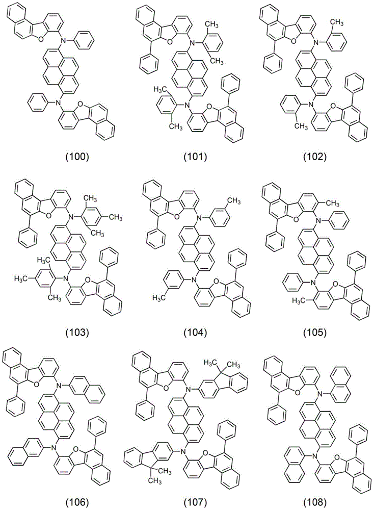
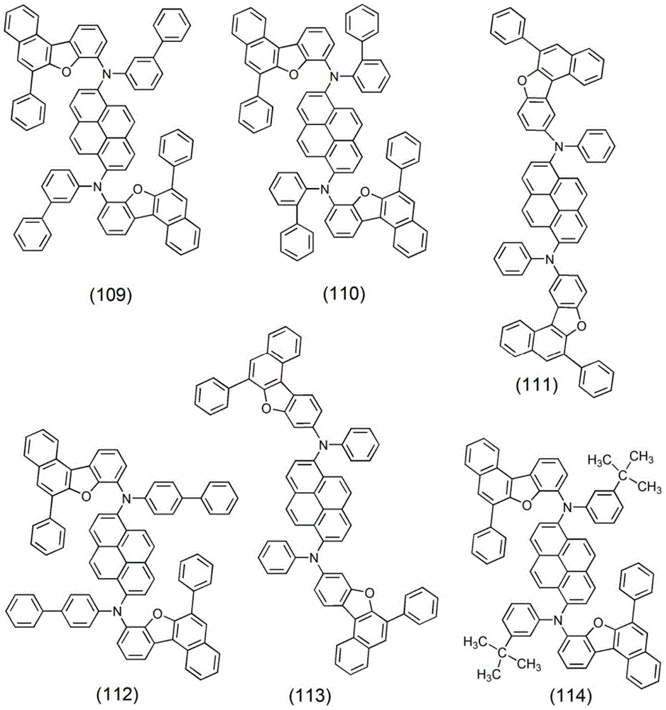
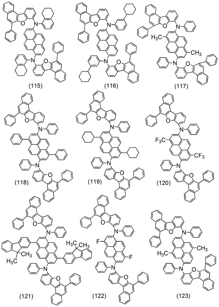
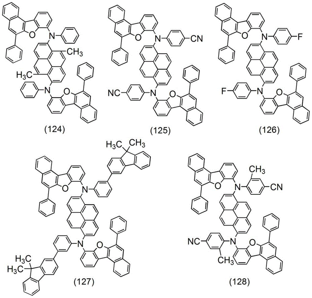

上述有机化合物呈现高色纯度的蓝色发光,可以得到NTSC(National TelevisionStandards Committee;美国国家电视标准委员会)所规定的蓝色色度(即,(x,y)=(0.14,0.08))附近或比其深的色纯度高的蓝色发光。因此,通过将这些有机化合物用于发光元件,能够实现驱动电压低且可靠性高的发光元件。再者,通过使用这种发光元件,可以实现本发明的一个方式的发光装置、电子设备及照明装置的低功耗化及长使用寿命化。The above-mentioned organic compound exhibits blue light emission with high color purity, and can obtain the blue chromaticity (that is, (x, y)=(0.14, 0.08)) specified by NTSC (National Television Standards Committee; National Television Standards Committee) near or higher than Its deep color and high purity blue glow. Therefore, by using these organic compounds for a light-emitting element, it is possible to realize a light-emitting element with low driving voltage and high reliability. Furthermore, by using such a light-emitting element, it is possible to achieve low power consumption and long service life of the light-emitting device, electronic equipment, and lighting device according to one aspect of the present invention.
本实施方式所示的结构可以与其他实施方式所示的结构适当地组合而实施。The structure shown in this embodiment mode can be implemented in combination with the structure shown in other embodiment mode as appropriate.
实施方式3Embodiment 3
在本实施方式中,说明将实施方式1所说明的发光元件与着色层(滤色片等)组合时的发光装置的一个方式。在本实施方式中,参照图5对发光装置的像素部的结构进行说明。In this embodiment mode, one mode of a light-emitting device in which the light-emitting element described in
在图5中,在衬底501上形成有多个FET502,各FET502与各发光元件(507R、507G、507B及507W)电连接。具体而言,各FET502与作为发光元件的像素电极的第一电极503电连接。另外,为了覆盖相邻的第一电极503的端部,设置有分隔壁504。In FIG. 5, a plurality of
本实施方式中的第一电极503具有反射电极的功能。在第一电极503上形成有EL层505,在EL层505上形成有第二电极510。EL层505包含呈现多个单色光的多个发光层,第二电极510具有半透射半反射电极的功能。The
各发光元件(507R、507G、507B及507W)发射不同的发光。具体而言,发光元件507R以得到红色光的方式被光学调整,在以506R表示的区域中穿过着色层508R向箭头方向射出红色光。发光元件507G以得到绿色光的方式被光学调整,在以506G表示的区域中穿过着色层508G向箭头方向射出绿色光。发光元件507B以得到蓝色光的方式被光学调整,在以506B表示的区域中穿过着色层508B向箭头方向射出蓝色光。发光元件507W以得到白色光的方式被光学调整,在以506W表示的区域中不穿过着色层向箭头方向射出白色光。Each light emitting element (507R, 507G, 507B, and 507W) emits different light emission. Specifically, the
如图5所示,各着色层(508R、508G、508B)设置在透明的密封衬底511上,该密封衬底511位于设置有各发光元件(507R、507G、507B、507W)的衬底501的上方。各着色层(508R、508G、508B)设置在与呈现各发光颜色的发光元件(507R、507G、507B)重叠的位置上。As shown in FIG. 5, each colored layer (508R, 508G, 508B) is provided on a
另外,以覆盖相邻的着色层(508R、508G、508B)的端部的方式设置有黑色层(黑矩阵)509。各着色层(508R、508G、508B)及黑色层509也可以被使用透明的材料的保护层覆盖。In addition, a black layer (black matrix) 509 is provided so as to cover the ends of adjacent colored layers ( 508R, 508G, 508B). Each colored layer (508R, 508G, 508B) and the
上述发光装置具有从密封衬底511一侧提取光的结构(顶部发射型),但是也可以具有从形成有FET的衬底501一侧提取光的结构(底部发射型)。本实施方式所示的顶部发射型发光装置可以作为衬底501使用遮光性衬底或透光性衬底,但是,底部发射型发光装置需要作为衬底501使用透光性衬底。The light emitting device described above has a structure in which light is extracted from the sealing
除了上述结构之外,还可以采用图10所示的结构。在图10中,与衬底501上的FET502电连接的发光元件(507R、507G、507B、507Y)的结构的一部分与图5不同。在实施方式1所示的EL层所包含的发光层中,采用作为发光层106a使用实施方式1所示的荧光发光物质而获得蓝色发光且作为发光层106b获得黄色发光的结构即可。In addition to the above-described structure, the structure shown in FIG. 10 may also be employed. In FIG. 10 , part of the structure of the light emitting elements ( 507R, 507G, 507B, 507Y ) electrically connected to the
此时,各发光元件(507R、507G、507B及507Y)发射不同的发光。具体而言,发光元件507R以得到红色光的方式被光学调整,在以506R表示的区域中穿过着色层508R向箭头方向射出红色光。发光元件507G以得到绿色光的方式被光学调整,在以506G表示的区域中穿过着色层508G向箭头方向射出绿色光。发光元件507B以得到蓝色光的方式被光学调整,在以506B表示的区域中穿过着色层508B向箭头方向射出蓝色光。发光元件507Y以得到黄色光的方式被光学调整,在以506Y表示的区域中穿过着色层508Y向箭头方向射出黄色光。At this time, each light emitting element (507R, 507G, 507B, and 507Y) emits different light emission. Specifically, the
如图10所示,各着色层(508R、508G、508B、508Y)设置在透明的密封衬底511上,该密封衬底511位于设置有各发光元件(507R、507G、507B、507Y)的衬底501之上方。各着色层(508R、508G、508B、508Y)设置在与呈现各发光颜色的发光元件(507R、507G、507B、507Y)重叠的位置上。As shown in FIG. 10, each colored layer (508R, 508G, 508B, 508Y) is provided on a
在本发明的一个方式中,从发光元件507B穿过着色层508B射出到发光装置外部的蓝色发光优选为深蓝色发光,即xy色度坐标中的色度为x=0.13以上0.17以下且y=0.03以上0.08以下。该y坐标更优选为0.03以上0.07以下。In one aspect of the present invention, the blue light emitted from the light-emitting
通过使用上述色度的蓝色发光,可以降低为了获得白色发光而需要的蓝色发光的亮度。因为为了获得规定的白色发光而由蓝色发光元件所消耗的电流量比其他的颜色的发光元件所消耗的电流量大得多,所以当为了获得白色发光而需要的蓝色发光的亮度降低时,就非常有效地降低电流量。By using blue light emission with the above-mentioned chromaticity, the brightness of blue light emission required to obtain white light emission can be reduced. Since the amount of current consumed by the blue light-emitting element in order to obtain the specified white light emission is much larger than that consumed by other color light-emitting elements, when the brightness of the blue light emission required to obtain white light emission decreases , it is very effective in reducing the amount of current.
当蓝色的色度改善时,该蓝色发光元件的电流效率通常降低,但是蓝色的色度改善带来的为了获得白色发光而需要的蓝色发光的亮度下降的效果更大。换言之,为了获得规定的白色发光而需要的蓝色发光元件的电流量大幅度地降低,发光装置整体的功耗也随之降低。When the chromaticity of blue is improved, the current efficiency of the blue light-emitting element generally decreases, but the improvement of chromaticity of blue has a greater effect of reducing the luminance of blue light emission required to obtain white light emission. In other words, the current amount of the blue light-emitting element required to obtain predetermined white light emission is greatly reduced, and the power consumption of the entire light-emitting device is also reduced accordingly.
另外,当蓝色发光的色度为上述深蓝色时,有时组合该蓝色发光与黄色发光而获得的发光的色调发生变化,而改变为了获得规定的白色发光而需要的第三发光的颜色。例如,在蓝色的色度为NTSC附近的发光颜色((x,y)=(0.14,0.08)附近)且黄色的色度为(x,y)=(0.45,0.54)附近的情况下,为了获得D65附近的白色发光,除了对组合蓝色发光与黄色发光而获得的发光以外还需要红色的发光成分。另一方面,在蓝色的色度为NTSC附近的情况下,如果黄色的色度为(x,y)=(0.46,0.53)或者更靠近红色的色度(即x更大且y更小的色度),就可以通过对组合蓝色发光与黄色发光而获得的发光追加绿色的发光成分来获得D65附近的白色发光。然而,如果黄色的色度比该色度更靠近红色(即,x大于0.46且y小于0.53),视见函数(luminosityfactor)下降而降低黄色像素的电流效率。换而言之,功耗的下降效果也相应地减少。Also, when the chromaticity of the blue light emission is the above-mentioned deep blue, the color tone of the light emission obtained by combining the blue light emission and the yellow light emission may change, and the color of the third light emission necessary to obtain predetermined white light emission may be changed. For example, when the chromaticity of blue is an emission color near NTSC (near (x, y)=(0.14, 0.08)) and the chromaticity of yellow is near (x, y)=(0.45, 0.54), In order to obtain white luminescence around D65, a red luminescent component is required in addition to luminescence obtained by combining blue luminescence and yellow luminescence. On the other hand, in the case where the chromaticity of blue is around NTSC, if the chromaticity of yellow is (x, y) = (0.46, 0.53) or closer to the chromaticity of red (ie, x is larger and y is smaller chromaticity), white light emission near D65 can be obtained by adding a green light emission component to the light emission obtained by combining blue light emission and yellow light emission. However, if the chromaticity of yellow is closer to red than the chromaticity (ie, x is greater than 0.46 and y is less than 0.53), the luminosity factor decreases to reduce the current efficiency of the yellow pixel. In other words, the reduction effect of power consumption is correspondingly reduced.
如此,蓝色发光与黄色发光的色调改变为了D65附近的白色发光而需要的第三发光的颜色。一般而言,绿色发光的电流效率比红色发光高,所以是有利的。但是,如上所述,当黄色的色度靠近红色时(即,x大于0.46且y小于0.53),该黄色发光的视见函数下降而降低黄色像素的电流效率。视见函数高的黄色发光的电流效率的下降的影响很大,所以使黄色发光的色度靠近红色是不宜的。In this way, the color tone of the blue light emission and the yellow light emission changes the color of the third light emission required for white light emission near D65. In general, the current efficiency of green light emission is higher than that of red light emission, which is advantageous. However, as described above, when the chromaticity of yellow is close to red (ie, x is greater than 0.46 and y is less than 0.53), the visibility function of the yellow light emission decreases to reduce the current efficiency of the yellow pixel. Since the decrease in the current efficiency of yellow light emission having a high visibility function has a large influence, it is not appropriate to bring the chromaticity of yellow light emission closer to red.
另一方面,当使用x=0.13以上0.17以下且y=0.03以上0.08以下的深蓝色发光时,在黄色发光保持视见函数高的色度(即,不太靠近红色的色度)的同时,可以通过使用蓝色发光、黄色发光以及作为第三发光的绿色发光来获得D65附近的白色发光。在该结构中,可以使用视见函数高的黄色发光,所以可以保持高电流效率。另外,与第三发光为红色发光的情况相比,该结构中的绿色发光所需要的亮度小。再者,绿色发光的视见函数比红色发光良好,并且,绿色发光元件的电流效率通常比红色发光元件的电流效率良好,因此为了获得第三发光而需要的电流量大幅度地降低。其结果,驱动电压也降低,所以可以降低功耗。此时的黄色发光的色度优选为x=0.44以上0.46以下且y=0.53以上0.55以下。On the other hand, when using dark blue light emission with x = 0.13 to 0.17 and y = 0.03 to 0.08, while yellow light emission maintains a chromaticity with a high visual function (that is, a chromaticity that is not too close to red), White luminescence near D65 can be obtained by using blue luminescence, yellow luminescence, and green luminescence as a third luminescence. In this structure, yellow light emission with a high visibility function can be used, so high current efficiency can be maintained. In addition, compared with the case where the third light emission is red light emission, the luminance required for green light emission in this structure is smaller. Furthermore, green light emission has a better viewing function than red light emission, and the current efficiency of green light emitting elements is generally better than that of red light emitting elements, so the amount of current required to obtain the third light emission is greatly reduced. As a result, the driving voltage is also reduced, so that power consumption can be reduced. At this time, the chromaticity of the yellow light emission is preferably x=0.44 to 0.46 and y=0.53 to 0.55.
通过增加黄色发光元件的亮度,可以补充用来获得规定的白色发光的蓝色发光元件及呈现第三发光的发光元件的亮度成分的下降。黄色发光的视见函数非常高且黄色发光元件的电流效率非常高,所以蓝色发光元件及呈现第三发光的发光元件的亮度下降带来的功耗降低抵消黄色发光所需要的亮度上升造成的功耗,所以可以实现低功耗化。By increasing the luminance of the yellow light-emitting element, it is possible to compensate for the decrease in the luminance components of the blue light-emitting element for obtaining predetermined white light emission and the light-emitting element exhibiting the third light emission. The visible function of yellow light emission is very high and the current efficiency of the yellow light-emitting element is very high, so the reduction in power consumption due to the decrease in brightness of the blue light-emitting element and the light-emitting element that emits the third light offsets the increase in brightness required for yellow light emission. power consumption, so low power consumption can be realized.
为了获得xy色度坐标中的色度为x=0.13以上0.17以下且y=0.03以上0.08以下,优选为x=0.13以上0.17以下且y=0.03以上0.07以下的深蓝色发光,第一发光元件所包含的荧光发光材料的甲苯溶液中的发射光谱的峰值波长为440nm至460nm,优选为440nm至455nm。蓝色发光元件的色度也可以利用滤色片等调节,上述波长的光即使穿过滤色片也不易被过滤掉,因此可以高效地利用来自荧光发光材料的发光。由于同样的原因,荧光发光材料的甲苯溶液中的发射光谱的半宽优选为20nm以上50nm以下。In order to obtain dark blue light with a chromaticity of x=0.13 to 0.17 and y=0.03 to 0.08 in the xy chromaticity coordinates, preferably x=0.13 to 0.17 and y=0.03 to 0.07, the first light emitting element The peak wavelength of the emission spectrum of the included fluorescent material in the toluene solution is 440nm to 460nm, preferably 440nm to 455nm. The chromaticity of the blue light-emitting element can also be adjusted by using a color filter, etc., and the light of the above-mentioned wavelength is not easily filtered out even if it passes through the color filter, so the luminescence from the fluorescent light-emitting material can be efficiently used. For the same reason, the half-width of the emission spectrum in the toluene solution of the fluorescent light-emitting material is preferably 20 nm or more and 50 nm or less.
通过使用具有上述色度的蓝色发光,可以降低为了获得D65附近的白色发光,即xy色度坐标中的色度为(0.313,0.329)的光而需要的功耗。具体而言,当以300cd/m2的亮度获得xy色度坐标中的色度为(0.313,0.329)的白色发光时,该发光装置的不包含驱动FET时的功耗可以为1mW/cm2以上7mW/cm2以下,包含驱动FET时的功耗(利用阳极-阴极之间的电压与耗电流之积算出的功耗)可以为2mW/cm2以上15mW/cm2以下。By using blue light emission having the above-mentioned chromaticity, power consumption required to obtain white light emission near D65, that is, light having a chromaticity of (0.313, 0.329) in the xy chromaticity coordinates can be reduced. Specifically, when white light with a chromaticity of (0.313, 0.329) in the xy chromaticity coordinates is obtained at a brightness of 300 cd/m 2 , the power consumption of the light emitting device without driving FETs can be 1 mW/cm 2 The above is 7mW/cm 2 or less, including the power consumption when driving FET (the power consumption calculated by the product of the voltage between the anode and the cathode and the current consumption) can be 2mW/cm 2 to 15mW/cm 2 .
通过采用上述结构,可以得到呈现多个发光颜色(红色、蓝色、绿色及黄色)的发光元件,与此同时得到能够发射组合上述发光的发光效率高的白色光的发光装置。By adopting the above structure, it is possible to obtain a light emitting element exhibiting a plurality of light emitting colors (red, blue, green, and yellow), and at the same time obtain a light emitting device capable of emitting white light with high luminous efficiency in combination with the above light emission.
本发明的一个方式的发光装置可以使用各种衬底制造。对衬底的种类没有特别的限制。作为衬底的一个例子,可以举出半导体衬底(例如,单晶衬底或硅衬底)、SOI衬底、玻璃衬底、石英衬底、塑料衬底、金属衬底、不锈钢衬底、具有不锈钢箔的衬底、钨衬底、具有钨箔的衬底、柔性衬底、贴合薄膜、包含纤维状的材料的纸或者基材薄膜等。作为玻璃衬底的例子,可以举出钡硼硅酸盐玻璃、铝硼硅酸盐玻璃、钠钙玻璃等。作为柔性衬底、贴合薄膜、基材薄膜等的例子,可以举出以聚对苯二甲酸乙二醇酯(PET)、聚萘二甲酸乙二醇酯(PEN)、聚醚砜(PES)、聚四氟乙烯(PTFE)为代表的塑料。此外,也可以使用丙烯酸树脂、聚丙烯、聚酯、聚氟化乙烯、聚氯乙烯、聚酰胺、聚酰亚胺、芳族聚酰胺、环氧、无机蒸镀薄膜、纸类等。The light-emitting device of one embodiment of the present invention can be produced using various substrates. There is no particular limitation on the kind of substrate. As an example of the substrate, a semiconductor substrate (for example, a single crystal substrate or a silicon substrate), an SOI substrate, a glass substrate, a quartz substrate, a plastic substrate, a metal substrate, a stainless steel substrate, Substrates with stainless steel foils, tungsten substrates, substrates with tungsten foils, flexible substrates, laminated films, paper or base films made of fibrous materials, and the like. Examples of the glass substrate include barium borosilicate glass, aluminoborosilicate glass, soda lime glass, and the like. As examples of flexible substrates, lamination films, base films, etc., polyethylene terephthalate (PET), polyethylene naphthalate (PEN), polyethersulfone (PES ), polytetrafluoroethylene (PTFE) as the representative plastics. In addition, acrylic resin, polypropylene, polyester, polyvinyl fluoride, polyvinyl chloride, polyamide, polyimide, aramid, epoxy, inorganic vapor-deposited film, paper, etc. can also be used.
通过使用半导体衬底、单晶衬底或SOI衬底等制造晶体管,可以制造特性、尺寸或形状等的不均匀性小、电流能力高且尺寸小的晶体管。当利用上述晶体管构成电路时,可以实现电路的低功耗化或电路的高集成化。By manufacturing transistors using semiconductor substrates, single crystal substrates, SOI substrates, etc., it is possible to manufacture transistors with small variations in characteristics, size, shape, etc., high current capability, and small size. When a circuit is configured using the above-mentioned transistors, it is possible to achieve low power consumption of the circuit or high integration of the circuit.
也可以在衬底上设置剥离层而形成晶体管等半导体装置。剥离层可以在如下情况下使用:在剥离层上制造半导体装置的一部分或全部,然后将其从衬底分离并转置到其他衬底上的情况。此时,也可以将晶体管转置到耐热性低的衬底或柔性衬底上。另外,作为上述剥离层,例如可以使用钨膜与氧化硅膜的无机膜的层叠结构或衬底上形成有聚酰亚胺等有机树脂膜的结构等。A release layer may be provided on a substrate to form a semiconductor device such as a transistor. The release layer can be used in the case of manufacturing a part or the whole of a semiconductor device on the release layer, and then separating it from the substrate and transposing it to another substrate. At this time, the transistor can also be transposed on a substrate with low heat resistance or a flexible substrate. In addition, as the above-mentioned release layer, for example, a lamination structure of an inorganic film of a tungsten film and a silicon oxide film, or a structure in which an organic resin film such as polyimide is formed on a substrate, or the like can be used.
也就是说,也可以使用一个衬底形成晶体管或发光元件,然后将该晶体管或发光元件转置到另一个衬底上。作为转置晶体管或发光元件的衬底,不仅可以使用上述可以形成晶体管的衬底,还可以使用纸衬底、玻璃纸衬底、芳族聚酰胺薄膜衬底、聚酰亚胺薄膜衬底、石材衬底、木材衬底、布衬底(包括天然纤维(丝、棉、麻)、合成纤维(尼龙、聚氨酯、聚酯)或再生纤维(醋酯纤维、铜氨纤维、人造纤维、再生聚酯)等)、皮革衬底、橡皮衬底等。通过使用上述衬底,可以实现特性良好的晶体管的形成、功耗低的晶体管的形成、不易损坏的装置的制造、耐热性的提高、轻量化或薄型化。另外,在制造柔性发光装置时,也可以在柔性衬底上直接形成晶体管或发光元件。That is, it is also possible to form a transistor or a light emitting element using one substrate, and then transfer the transistor or light emitting element to another substrate. As a substrate for transposing transistors or light-emitting elements, not only the above-mentioned substrates on which transistors can be formed, but also paper substrates, cellophane substrates, aramid film substrates, polyimide film substrates, stone materials, etc. Backing, wood backing, cloth backing (including natural fibers (silk, cotton, hemp), synthetic fibers (nylon, polyurethane, polyester) or recycled fibers (acetate, cupro, rayon, recycled polyester ), etc.), leather backing, rubber backing, etc. By using the above-mentioned substrate, it is possible to form a transistor with good characteristics, form a transistor with low power consumption, manufacture a device that is not easily damaged, improve heat resistance, and reduce weight or thickness. In addition, when manufacturing a flexible light-emitting device, transistors or light-emitting elements can also be directly formed on a flexible substrate.
本实施方式所示的结构可以与其他实施方式所示的结构适当地组合而实施。The structure shown in this embodiment mode can be implemented in combination with the structure shown in other embodiment mode as appropriate.
实施方式4
在本实施方式中,对包含本发明的一个方式的发光元件的发光装置进行说明。In this embodiment mode, a light-emitting device including a light-emitting element according to one embodiment of the present invention will be described.
上述发光装置既可以是无源矩阵型发光装置,又可以是有源矩阵型发光装置。此外,可以将其他的实施方式所说明的发光元件应用于本实施方式所示的发光装置。The above light emitting device may be either a passive matrix light emitting device or an active matrix light emitting device. In addition, the light-emitting elements described in other embodiments can be applied to the light-emitting device described in this embodiment.
在本实施方式中,参照图6A和图6B对有源矩阵型发光装置进行说明。In this embodiment mode, an active matrix light emitting device will be described with reference to FIGS. 6A and 6B .
图6A是发光装置的俯视图,图6B是沿着图6A中的虚线A-A’切割的截面图。本实施方式的有源矩阵型发光装置具有设置在元件衬底601上的像素部602、驱动电路部(源极线驱动电路)603以及驱动电路部(栅极线驱动电路)604a及604b。将像素部602、驱动电路部603以及驱动电路部604a及604b由密封剂605密封在元件衬底601与密封衬底606之间。FIG. 6A is a top view of the light emitting device, and FIG. 6B is a cross-sectional view cut along the dotted line A-A' in FIG. 6A. The active matrix light-emitting device of this embodiment includes a
在元件衬底601上设置有引导布线607,该引导布线607用来连接对驱动电路部603及驱动电路部604a及604b传递来自外部的信号(例如,视频信号、时钟信号、起始信号或复位信号等)或电位的外部输入端子。在此,示出作为外部输入端子设置FPC(柔性印刷电路)608的例子。虽然在此只图示FPC,但是该FPC也可以安装有印刷线路板(PWB)。本说明书中的发光装置不仅包括发光装置主体,而且还包括安装有FPC或PWB的发光装置。A
接着,参照图6B说明截面结构。在元件衬底601上形成有驱动电路部及像素部,在此示出作为源极线驱动电路的驱动电路部603及像素部602。Next, the cross-sectional structure will be described with reference to FIG. 6B . A driver circuit unit and a pixel unit are formed on an
在此示出组合FET609和FET610构成驱动电路部603的例子。驱动电路部603既可以由包含单极性(N型或P型)晶体管的电路形成,也可以由包含N型晶体管及P型晶体管的CMOS电路形成。在本实施方式中,虽然示出将驱动电路形成在衬底上的驱动器一体型,但是也可以将驱动电路形成在衬底的外部。Here, an example in which the
此外,像素部602由多个像素构成,该像素各包括开关FET611、电流控制FET612以及与电流控制FET612的布线(源电极或漏电极)电连接的第一电极(阳极)613。虽然在本实施方式中示出开关FET611及电流控制FET612的两个FET构成像素部602的例子,但不局限于此。例如,像素部602也可以包含三个以上的FET及电容元件。Also, the
作为FET609、610、611及612,例如可以适当地使用交错型晶体管或反交错型晶体管。作为可以用于FET609、610、611及612的半导体材料,例如可以使用第13族(镓等)半导体、第14族(硅等)半导体、化合物半导体、氧化物半导体、有机半导体。此外,对该半导体材料的结晶性没有特别的限制,例如可以使用非晶半导体或结晶半导体。尤其是,FET609、610、611及612优选使用氧化物半导体。作为该氧化物半导体,例如可以举出In-Ga氧化物、In-M-Zn氧化物(M为Al、Ga、Y、Zr、La、Ce或Nd)等。作为FET609、610、611及612,例如使用能隙为2eV以上,优选为2.5eV以上,更优选为3eV以上的氧化物半导体材料,由此可以降低晶体管的关态电流(off-state current)。As the
此外,以覆盖第一电极613的端部的方式形成有绝缘物614。在此,使用正型光敏丙烯酸树脂形成绝缘物614。此外,在本实施方式中,将第一电极613用作阳极。In addition, an
优选将绝缘物614的上端部或下端部形成为具有曲率的曲面。通过将绝缘物614形成为上述形状,可以提高形成在绝缘物614上的膜的覆盖性。例如,作为绝缘物614的材料,可以使用负型光敏树脂或正型光敏树脂,不局限于有机化合物,而还可以使用无机化合物诸如氧化硅、氧氮化硅、氮化硅等。It is preferable to form the upper end or the lower end of the
在第一电极(阳极)613上层叠有EL层615及第二电极(阴极)616。EL层615至少包含发光层。EL层615除了发光层以外还可以适当地包含空穴注入层、空穴传输层、电子传输层、电子注入层和电荷产生层等。An
由第一电极(阳极)613、EL层615及第二电极(阴极)616的叠层结构形成发光元件617。作为第一电极(阳极)613、EL层615及第二电极(阴极)616的材料,可以使用实施方式1所示的材料。另外,虽然未图示,但是第二电极(阴极)616与外部输入端子的FPC608电连接。A light-emitting
虽然在图6B所示的截面图中仅示出一个发光元件617,但是,在像素部602中多个发光元件被配置为矩阵状。通过在像素部602中选择性地形成能够得到三种(R、G、B)颜色的发光的发光元件,可以形成能够进行全彩色显示的发光装置。此外,除了可以得到三种(R、G、B)颜色的发光的发光元件以外,例如也可以形成能够得到白色(W)、黄色(Y)、品红色(M)、青色(C)等颜色的发光的发光元件。例如,通过对能够得到三种(R、G、B)颜色的发光的发光元件追加上述能够得到多种发光的发光元件,可以获得色纯度的提高、功耗的降低等的效果。此外,也可以通过与滤色片组合来实现能够进行全彩色显示的发光装置。再者,也可以通过与量子点组合来提供发光效率得到提高且功耗得到降低的发光装置。Although only one
再者,通过使用密封剂605将密封衬底606与元件衬底601贴合在一起,实现在由元件衬底601、密封衬底606和密封剂605围绕的空间618中具备发光元件617的结构。另外,空间618可以填充有惰性气体(氮、氩等),也可以填充有密封剂605。Furthermore, by bonding the sealing
优选将环氧类树脂或玻璃料用作密封剂605。此外,这些材料优选尽量不使水分和氧透过。此外,作为密封衬底606,除了玻璃衬底和石英衬底之外,还可以使用由FRP(Fiber-Reinforced Plastics:纤维增强塑料)、PVF(polyvinyl fluoride:聚氟乙烯)、聚酯、丙烯酸树脂等构成的塑料衬底等在实施方式3中例示出的衬底。从粘合性的观点来看,在作为密封剂使用玻璃料的情况下,作为元件衬底601及密封衬底606优选使用玻璃衬底。Epoxy resin or glass frit is preferably used as the
如上所述,可以得到有源矩阵型发光装置。As described above, an active matrix type light emitting device can be obtained.
本实施方式所示的结构可以与其他实施方式所示的结构适当地组合而实施。The structure shown in this embodiment mode can be implemented in combination with the structure shown in other embodiment mode as appropriate.
实施方式5Embodiment 5
在本实施方式中,使用图7A至图7D′-2对使用本发明的一个方式的发光装置而完成的各种各样的电子设备的例子进行说明。In this embodiment, examples of various electronic devices completed using the light-emitting device of one embodiment of the present invention will be described with reference to FIGS. 7A to 7D′-2.
作为使用发光装置的电子设备,例如可以举出电视装置(也称为电视或电视接收机)、用于计算机等的显示器、例如数码相机、数码摄像机的相机、数码相框、移动电话机(也称为移动电话、移动电话装置)、便携式游戏机、便携式信息终端、音频再现装置、弹珠机等的大型游戏机等。图7A至图7D′-2示出上述电子设备的具体例子。Examples of electronic equipment using light-emitting devices include television sets (also called televisions or television receivers), displays for computers, etc., cameras such as digital cameras and digital video cameras, digital photo frames, mobile phones (also called Large-scale game machines such as mobile phones, mobile phone devices), portable game machines, portable information terminals, audio reproduction devices, pachinko machines, etc. 7A to 7D'-2 show specific examples of the above-mentioned electronic equipment.
图7A示出电视装置的一个例子。在电视装置7100中,外壳7101中组装有显示部7103。由显示部7103能够显示影像,显示部7103也可以为安装有触摸传感器(输入装置)的触控面板(输入输出装置)。可以将本发明的一个方式的发光装置用于显示部7103。在此示出利用支架7105支撑外壳7101的结构。FIG. 7A shows an example of a television set. In
通过利用外壳7101所具备的操作开关、或另外提供的遥控操作机7110可以进行电视装置7100的操作。通过利用遥控操作机7110所具备的操作键7109,可以进行频道、音量的操作,并可以对在显示部7103上显示的图像进行操作。此外,也可以采用在遥控操作机7110中设置显示从该遥控操作机7110输出的信息的显示部7107的结构。The
电视装置7100采用具备接收机、调制解调器等的结构。通过接收机可以接收一般的电视广播。再者,通过调制解调器连接到有线或无线方式的通信网络,可以进行单向(从发送者到接收者)或双向(发送者和接收者之间或接收者彼此之间等)的信息通信。
图7B为计算机,该计算机包括主体7201、外壳7202、显示部7203、键盘7204、外部连接端口7205、指向装置7206等。该计算机可以通过将本发明的一个方式的发光装置用于其显示部7203来制造。显示部7203也可以为安装有触摸传感器(输入装置)的触控面板(输入输出装置)。7B is a computer, which includes a
图7C是智能手表,该智能手表包括外壳7302、显示面板7304、操作按钮7311、操作按钮7312、连接端子7313、腕带7321、表带扣7322等。7C is a smart watch, which includes a
安装在兼用作框架(bezel)部分的外壳7302中的显示面板7304具有非矩形状的显示区域。显示面板7304可以显示表示时间的图标7305以及其他图标7306等。显示面板7304也可以为安装有触摸传感器(输入装置)的触控面板(输入输出装置)。A
在图7C所示的智能手表可以具有各种功能。例如,可以具有在显示部上显示各种信息(静态图像、运动图像、文字图像等)的功能;触控面板功能;显示日历、日期或时间等的功能;以各种软件(程序)控制处理的功能;无线通信功能;使用无线通信功能与各种计算机网络连接的功能;使用无线通信功能发送及接收各种数据的功能;以及读出储存于存储介质内的程序或数据并且将该程序或数据显示于显示部上的功能等。The smart watch shown in FIG. 7C can have various functions. For example, it may have the function of displaying various information (still images, moving images, text images, etc.) on the display unit; the function of the touch panel; the function of displaying the calendar, date, time, etc.; functions; wireless communication functions; functions of connecting with various computer networks using wireless communication functions; functions of sending and receiving various data using wireless communication functions; A function to display data on the display unit, etc.
外壳7302的内部可具有扬声器、传感器(具有测定如下因素的功能的传感器:力量、位移、位置、速度、加速度、角速度、转速、距离、光、液、磁、温度、化学物质、声音、时间、硬度、电场、电流、电压、电力、辐射线、流量、湿度、斜率、振动、气味或红外线)、麦克风等。另外,智能手表可以通过将发光装置用于其显示面板7304来制造。The interior of the
图7D示出移动电话机(包括智能手机)的一个例子。移动电话机7400在外壳7401中具备显示部7402、麦克风7406、扬声器7405、照相机7407、外部连接部7404、操作按钮7403等。当将本发明的一个方式的发光元件形成在柔性衬底上来制造发光装置时,发光元件可以应用于如图7D所示那样的具有曲面的显示部7402。FIG. 7D shows an example of a mobile phone (including a smartphone). The
图7D所示的移动电话机7400可以用手指等触摸显示部7402来输入信息。此外,可以用手指等触摸显示部7402来进行打电话或制作电子邮件等的操作。
显示部7402的屏幕主要有如下三种模式:第一种是以图像显示为主的显示模式;第二种是以文字等信息输入为主的输入模式;第三种是混合显示模式与输入模式的两种模式的显示及输入模式。The screen of the
例如,在打电话或制作电子邮件的情况下,将显示部7402设定为以文字输入为主的文字输入模式,并进行显示在屏幕的文字的输入操作,即可。在此情况下,优选的是,在显示部7402的屏幕的大部分上显示键盘或号码按钮。For example, when making a phone call or creating an e-mail, it is sufficient to set the
另外,通过在移动电话机7400内部设置陀螺仪传感器和加速度传感器等检测装置,判断移动电话机7400的方向(纵向或横向),而可以对显示部7402的屏幕显示进行自动切换。In addition, by providing detection devices such as a gyro sensor and an acceleration sensor inside the
通过触摸显示部7402或对外壳7401的操作按钮7403进行操作,切换屏幕模式。或者,可以根据显示在显示部7402上的图像的类型而切换屏幕模式。例如,当显示在显示部上的图像为运动图像时,将屏幕模式切换成显示模式,而当显示在显示部上的图像为文字时,将屏幕模式切换成输入模式。The screen mode is switched by touching the
另外,当在输入模式下通过检测出显示部7402的光传感器所检测的信号得知在一定期间内没有显示部7402的触摸操作输入时,也可以进行控制以将画面模式从输入模式切换成显示模式。In addition, when it is known that there is no touch operation input on the
还可以将显示部7402用作图像传感器。例如,通过用手掌或手指触摸显示部7402,来拍摄掌纹、指纹等,而可以进行个人识别。另外,通过将发出近红外光的背光源或发出近红外光的传感用光源用于显示部,还可以拍摄手指静脉、手掌静脉等。The
再者,也可以将发光装置应用于作为移动电话机(包括智能手机)的其他结构的图7D′-1和图7D′-2所示的移动电话机。Furthermore, the light emitting device can also be applied to mobile phones shown in FIGS. 7D'-1 and 7D'-2 as other structures of mobile phones (including smart phones).
在图7D′-1和图7D′-2所示的移动电话机中,不仅在外壳7500(1)、外壳7500(2)的第一面7501(1)、第一面7501(2)上,而且能够在第二面7502(1)、第二面7502(2)上显示文字信息或图像信息等。借助于这种结构,使用者能够在将移动电话机收纳在上衣口袋中的状态下容易确认在第二面7502(1)、第二面7502(2)等上显示的文字信息或图像信息等。In the mobile phone shown in Fig. 7D'-1 and Fig. 7D'-2, not only on the first surface 7501(1) and the first surface 7501(2) of the casing 7500(1) and the casing 7500(2), , and text information, image information, etc. can be displayed on the second surface 7502(1) and the second surface 7502(2). With this structure, the user can easily confirm the text information or image information displayed on the second surface 7502(1), the second surface 7502(2) and the like while storing the mobile phone in the jacket pocket. .
图8A至图8C示出能够折叠的便携式信息终端9310。图8A示出展开状态的便携式信息终端9310。图8B示出正在被展开或被折叠的便携式信息终端9310。图8C示出折叠状态的便携式信息终端9310。便携式信息终端9310在折叠状态下可携带性好,在展开状态下因为具有无缝拼接的较大的显示区域所以显示一览性强。8A to 8C show a
显示面板9311由铰链部9313所连接的三个外壳9315支撑。显示面板9311也可以为安装有触摸传感器(输入装置)的触控面板(输入输出装置)。通过在两个外壳9315之间的铰链部9313处弯折显示面板9311,可以使便携式信息终端9310从展开状态可逆性地变为折叠状态。可以将本发明的一个方式的发光装置用于显示面板9311。显示面板9311中的显示区域9312是位于折叠状态的便携式信息终端9310的侧面的显示区域9312。在显示区域9312中可以显示信息图标、使用次数多的软件或程序的快捷等,能够顺便地进行确认信息或开启软件。The
如上所述,可以使用本发明的一个方式的发光装置得到电子设备。能够应用的电子设备不局限于在本实施方式中所示的电子设备,可以应用于各种领域的电子设备。As described above, electronic equipment can be obtained using the light-emitting device of one embodiment of the present invention. Applicable electronic devices are not limited to the electronic devices shown in this embodiment, and can be applied to electronic devices in various fields.
实施方式6
在本实施方式中,使用图9对使用本发明的一个方式的发光装置的照明装置的例子进行说明。In this embodiment, an example of a lighting device using a light emitting device according to one embodiment of the present invention will be described with reference to FIG. 9 .
图9是将发光装置用于室内照明装置8001的例子。因为发光装置可以实现大面积化,所以也可以形成大面积的照明装置。此外,也可以通过使用具有曲面的外壳来形成具有外壳、覆盖物及支架且发光区域具有曲面的照明装置8002。包括在本实施方式所示的发光装置中的发光元件为薄膜状,所以外壳的设计的自由度高。因此,可以形成能够对应各种设计的照明装置。再者,室内的墙面也可以设置有大型的照明装置8003。FIG. 9 shows an example in which a light emitting device is used in an
通过将发光装置用于桌子的表面,可以提供具有桌子的功能的照明装置8004。此外,通过将发光装置用于其他家具的一部分,可以提供具有家具的功能的照明装置。By using a light emitting device on the surface of the table, it is possible to provide the
如上所述,可以得到应用发光装置的各种各样的照明装置。这种照明装置包括在本发明的一个方式中。As described above, various lighting devices using light emitting devices are available. Such a lighting device is included in one aspect of the present invention.
本实施方式所示的结构可以与其他实施方式所示的结构适当地组合而使用。The structure shown in this embodiment mode can be used in combination with the structure shown in other embodiment mode as appropriate.
实施方式7Embodiment 7
在本实施方式中,参照图11A至图15对包含本发明的一个方式的发光元件或本发明的一个方式的发光装置的触控面板进行说明。In this embodiment, a touch panel including a light-emitting element according to one embodiment of the present invention or a light-emitting device according to one embodiment of the present invention will be described with reference to FIGS. 11A to 15 .
图11A和图11B是触控面板2000的透视图。注意,在图11A和图11B中,为了容易理解,示出触控面板2000的典型的构成要素。11A and 11B are perspective views of the
触控面板2000具备显示部2501及触摸传感器2595(参照图11B)。触控面板2000还具有衬底2510、衬底2570以及衬底2590。衬底2510、衬底2570以及衬底2590都具有柔性。
显示部2501包括衬底2510上的多个像素以及能够向该像素供应信号的多个布线2511。多个布线2511被引导到衬底2510的外周部,其一部分构成端子2519。端子2519与FPC2509(1)电连接。The
衬底2590具备触摸传感器2595以及多个与触摸传感器2595电连接的布线2598。多个布线2598被引导在衬底2590的外周部,其一部分构成连接层2599。连接层2599与FPC2509(2)电连接。另外,为了容易理解,在图11B中由实线示出设置在衬底2590的背面一侧的触摸传感器2595的电极以及布线等。The
作为触摸传感器2595,例如可以使用电容式触摸传感器。作为电容式触摸传感器,可以举出表面电容式触摸传感器、投影电容式触摸传感器等。As the
作为投影电容式触摸传感器,可以举出自电容式触摸传感器、互电容式触摸传感器等,这些主要根据驱动方式的差异而区分。当使用互电容式触摸传感器时,可以同时进行多点检测,所以是优选的。Examples of projected capacitive touch sensors include self-capacitive touch sensors, mutual capacitive touch sensors, and the like, and these are mainly distinguished by differences in driving methods. When a mutual capacitive touch sensor is used, multi-point detection can be performed simultaneously, which is preferable.
首先,参照图11B对采用投影电容式触摸传感器的情况进行说明。投影电容式触摸传感器可以应用能够检测出指头等检测对象的靠近或接触的各种传感器。First, a case where a projected capacitive touch sensor is used will be described with reference to FIG. 11B . Various sensors capable of detecting approach or contact of a detection target such as a finger can be applied to the projected capacitive touch sensor.
投影电容式触摸传感器2595具有电极2591及电极2592。电极2591及电极2592分别与多个布线2598中的不同的布线电连接。如图11A和图11B所示,电极2592具有在一个方向上连续地配置的多个四边形的每个角部通过布线2594相互连接的形状。电极2591也同样地具有多个四边形的角部连接的形状,但是电极2591的连接方向与电极2592的连接方向交叉。注意,电极2591的连接方向与电极2592的连接方向不一定需要相互垂直,它们之间的角度也可以为大于0度小于90度。The projected
优选尽量减小布线2594与电极2592的交叉部的面积。由此,可以减小没有设置电极的区域的面积,从而可以降低透射率的不均匀。其结果,可以降低透过触摸传感器2595的光的亮度不均匀。It is preferable to reduce the area of the intersection of the
另外,电极2591及电极2592的形状不局限于此,可以具有各种形状。例如,也可以以尽量没有间隙的方式配置多个电极2591,并且隔着绝缘膜设置多个电极2592。此时,通过在相邻的两个电极2592之间设置与它们电绝缘的虚拟电极,可以减小透射率不同的区域的面积,所以是优选的。In addition, the shapes of the
接着,参照图12A和图12B对触控面板2000进行详细说明。图12A相当于图11A所示的点划线X1-X2之间的截面图。Next, the
触摸传感器2595包括衬底2590上的配置为交错形状的电极2591及电极2592、覆盖电极2591及电极2592的绝缘层2593以及使相邻的电极2591电连接的布线2594。
在布线2594之下设置有粘合层2597。粘合层2597以触摸传感器2595与显示部2501重叠的方式将衬底2590贴合于衬底2570。An
电极2591及电极2592使用透光导电材料形成。作为透光导电材料,可以使用氧化铟、铟锡氧化物、铟锌氧化物、氧化锌、添加有镓的氧化锌等导电氧化物。另外,也可以使用包含石墨烯的膜。包含石墨烯的膜例如可以通过使膜状的氧化石墨烯还原来形成。作为还原方法,可以采用进行加热的方法等。The
例如,在通过溅射法在衬底2590上形成透光导电材料之后,可以通过光刻法等各种图案化技术去除不需要的部分来形成电极2591及电极2592。For example, after forming a light-transmitting conductive material on the
作为绝缘层2593的材料,例如,除了丙烯酸树脂、环氧树脂、具有硅氧烷键的树脂之外,还可以使用氧化硅、氧氮化硅、氧化铝等无机绝缘材料。As a material of the insulating
通过在设置在绝缘层2593中的开口部中形成布线2594,来使相邻的电极2591电连接。作为布线2594优选使用透光导电材料,因为可以提高触控面板的开口率。另外,作为布线2594优选使用其导电性高于电极2591及电极2592的材料,因为可以降低电阻。
相邻的电极2591通过布线2594彼此电连接。另外,相邻的电极2591之间设置有电极2592。
布线2598与电极2591或电极2592电连接。布线2598的一部分被用作端子。布线2598例如可以使用金属材料诸如铝、金、铂、银、镍、钛、钨、铬、钼、铁、钴、铜或钯等或者包含该金属材料的合金材料。The
通过连接层2599使布线2598与FPC2509(2)电连接。连接层2599可以使用各种各向异性导电膜(ACF:Anisotropic Conductive Film)、各向异性导电膏(ACP:AnisotropicConductive Paste)等。The
粘合层2597具有透光性。例如,可以使用热固化树脂、紫外线固化树脂,具体而言,可以使用丙烯酸类树脂、聚氨酯类树脂、环氧类树脂或硅氧烷类树脂等。The
显示部2501具备配置为矩阵状的多个像素。该像素具备显示元件及驱动该显示元件的像素电路。The
作为衬底2510及衬底2570例如可以使用水蒸气透过率为10-5g/(m2·天)以下,优选为10-6g/(m2·天)以下的柔性材料。另外,优选的是作为衬底2510及衬底2570使用热膨胀率大致相同的材料。例如,衬底2510及衬底2570都可以使用线性膨胀系数为1×10-3/K以下,优选为5×10-5/K以下,更优选为1×10-5/K以下的材料。As the
密封层2560的折射率优选比空气大。The
显示部2501包含像素2502R。像素2502R包含发光模块2580R。The
像素2502R具备发光元件2550R以及能够向发光元件2550R供应电力的晶体管2502t。晶体管2502t被用作像素电路的一部分。发光模块2580R具备发光元件2550R以及着色层2567R。The
发光元件2550R包括下部电极、上部电极以及下部电极与上部电极之间的EL层。The
另外,在密封层2560设置在提取光的一侧的情况下,密封层2560接触于发光元件2550R及着色层2567R。In addition, when the
着色层2567R位于与发光元件2550R重叠的位置。由此,发光元件2550R所发射的光的一部分透过着色层2567R,而向图12A所示的箭头的方向发射到发光模块2580R的外部。The
显示部2501在光的发射方向上设置有遮光层2567BM。以包围着色层2567R的方式设置有遮光层2567BM。The
显示部2501在与像素重叠的位置具备反射防止层2567p。作为反射防止层2567p,例如可以使用圆偏振片。The
显示部2501具备绝缘层2521。该绝缘层2521覆盖晶体管2502t。绝缘层2521具有使起因于像素电路的凹凸平坦化的功能。此外,也可以使绝缘层2521具有抑制杂质扩散的功能。由此,能够抑制因杂质的扩散而导致的晶体管2502t等的可靠性下降。The
发光元件2550R形成在绝缘层2521上。在发光元件2550R所具有的下部电极上设置有与该下部电极的端部重叠的分隔壁2528。另外,也可以在分隔壁2528上形成用来控制衬底2510与衬底2570的间隔的间隔物。The
扫描线驱动电路2503g(1)包括晶体管2503t以及电容器2503c。可以通过与像素电路相同的制造工序在相同的衬底上形成驱动电路。Scanning
在衬底2510上设置有能够供应信号的布线2511。布线2511上设置有端子2519。端子2519与FPC2509(1)电连接。FPC2509(1)具有供应图像信号及同步信号等信号的功能。FPC2509(1)也可以安装有印刷线路板(PWB)。
在显示部2501中,可以使用各种结构的晶体管。图12A示出使用底栅型晶体管的情况。例如,图12A所示的晶体管2502t及晶体管2503t可以使用包含氧化物半导体的半导体层作为沟道区。或者,晶体管2502t及晶体管2503t也可以使用包含非晶硅的半导体层作为沟道区。或者,晶体管2502t及晶体管2503t还可以使用包含通过激光退火法等处理结晶化了的多晶硅的半导体层作为沟道区。In the
另外,图12B示出使用顶栅型晶体管时的显示部2501的结构。In addition, FIG. 12B shows the structure of the
当使用顶栅型晶体管时,除了可用于底栅型晶体管的半导体层之外,还可以使用包含多晶硅或从单晶硅衬底等转置到的单晶硅膜等的半导体层作为沟道区。When using a top gate type transistor, in addition to the semiconductor layer that can be used for a bottom gate type transistor, a semiconductor layer including polysilicon or a single crystal silicon film or the like transposed from a single crystal silicon substrate or the like can be used as a channel region .
接着,参照图13A和图13B对与图12A和图12B不同结构的触控面板进行说明。Next, a touch panel having a structure different from that in FIGS. 12A and 12B will be described with reference to FIGS. 13A and 13B .
图13A和图13B是触控面板2001的截面图。图13A和图13B所示的触控面板2001与图12A和图12B所示的触控面板2000的不同之处为相对于显示部2501的触摸传感器2595的位置。在此,对不同之处进行详细说明,关于可以使用同样的结构的部分,援用触控面板2000的说明。13A and 13B are cross-sectional views of the
着色层2567R位于与发光元件2550R重叠的位置。图13A所示的发光元件2550R向设置有晶体管2502t的一侧发射光。由此,发光元件2550R发射的光的一部分透过着色层2567R,而向在图13A中的箭头的方向发射到发光模块2580R的外部。The
显示部2501在光的发射方向上具有遮光层2567BM。以包围着色层2567R的方式设置有遮光层2567BM。The
触摸传感器2595设置在显示部2501的衬底2510一侧(参照图13A)。The
粘合层2597设置在衬底2510与衬底2590之间,贴合显示部2501和触摸传感器2595。
在显示部2501中,可以使用各种结构的晶体管。图13A示出使用底栅型晶体管的情况。图13B示出使用顶栅型晶体管的情况。In the
接着,参照图14A和图14B对触控面板的驱动方法的一个例子进行说明。Next, an example of a method of driving the touch panel will be described with reference to FIGS. 14A and 14B .
图14A是示出互电容式触摸传感器的结构的方框图。在图14A中,示出脉冲电压输出电路2601、电流检测电路2602。另外,在图14A中,以6个布线X1至X6表示被施加脉冲电压的电极2621,并以6个布线Y1至Y6表示检测电流的变化的电极2622。此外,在图14A中,示出使电极2621与电极2622重叠而形成的电容器2603。注意,电极2621与电极2622的功能可以互相调换。FIG. 14A is a block diagram showing the structure of a mutual capacitive touch sensor. In FIG. 14A , a pulse
脉冲电压输出电路2601是用来依次将脉冲施加到布线X1至X6的电路。当对布线X1至X6施加脉冲电压时,在形成电容器2603的电极2621与电极2622之间产生电场。当在该电极之间产生的电场被遮蔽等时,产生电容器2603的互电容变化,通过利用该变化,可以检测检测对象的靠近或接触。The pulse
电流检测电路2602是用来检测电容器2603的互电容变化所引起的布线Y1至Y6的电流变化的电路。在布线Y1至Y6中,如果没有检测对象的靠近或接触,则所检测的电流值不发生变化,另一方面,在由于检测对象的靠近或接触而互电容减少的情况下,所检测的电流值减少。另外,通过积分电路等检测电流即可。The
接着,图14B示出图14A所示的互电容式触摸传感器中的输入/输出波形的时序图。在图14B中,在一个帧期间中进行各行列中的检测对象的检测。另外,在图14B中,示出没有检测出检测对象(未触摸)时和检测出检测对象(触摸)时的两种情况。此外,布线Y1至Y6的波形表示对应于所检测出的电流值的电压值。Next, FIG. 14B shows a timing chart of input/output waveforms in the mutual capacitive touch sensor shown in FIG. 14A . In FIG. 14B , detection of detection targets in each row and column is performed within one frame period. In addition, in FIG. 14B , two cases are shown when the detection target is not detected (no touch) and when the detection target is detected (touch). In addition, the waveforms of the wirings Y1 to Y6 represent voltage values corresponding to the detected current values.
依次对布线X1至X6施加脉冲电压,布线Y1至Y6的波形根据该脉冲电压而变化。当没有检测对象的靠近或接触时,布线Y1至Y6的波形根据布线X1至X6的电压变化而变化。另一方面,在有检测对象靠近或接触的部分电流值减少,因而与其相应的电压值的波形也产生变化。如此,通过检测互电容的变化,可以检测检测对象的靠近或接触。A pulse voltage is sequentially applied to the wirings X1 to X6, and the waveforms of the wirings Y1 to Y6 change according to the pulse voltage. When there is no approach or contact of the detection object, the waveforms of the wirings Y1 to Y6 change according to the voltage changes of the wirings X1 to X6 . On the other hand, the current value decreases at the portion where the object to be detected approaches or touches, so the waveform of the corresponding voltage value also changes. In this way, by detecting a change in mutual capacitance, it is possible to detect approach or contact of a detection object.
作为触摸传感器,图14A虽然示出仅在布线的交叉部设置电容器2603的无源型触摸传感器的结构,但是也可以采用具备晶体管和电容器的有源型触摸传感器。图15示出有源型触摸传感器所包括的一个传感器电路的例子。As a touch sensor, although FIG. 14A shows a passive touch sensor structure in which
图15所示的传感器电路包括电容器2603、晶体管2611、晶体管2612及晶体管2613。The sensor circuit shown in FIG. 15 includes a
对晶体管2613的栅极施加信号G2,对晶体管2613的源极和漏极中的一个施加电压VRES,并且晶体管2613的源极和漏极中的另一个与电容器2603的一个电极及晶体管2611的栅极电连接。晶体管2611的源极和漏极中的一个与晶体管2612的源极和漏极中的一个电连接,对另一个施加电压VSS。对晶体管2612的栅极施加信号G1,晶体管2612的源极和漏极中的另一个与布线ML电连接。对电容器2603的另一个电极施加电压VSS。The signal G2 is applied to the gate of the
接着,对图15所示的传感器电路的工作进行说明。首先,通过作为信号G2施加使晶体管2613成为开启状态的电位,对应于电压VRES的电位被施加到与晶体管2611的栅极连接的节点n。接着,通过作为信号G2施加使晶体管2613成为关闭状态的电位,节点n的电位得到保持。接着,由于手指等检测对象的靠近或接触,电容器2603的互电容产生变化,节点n的电位随之从VRES变化。Next, the operation of the sensor circuit shown in FIG. 15 will be described. First, by applying a potential to turn on the
在读出工作中,作为信号G1施加使晶体管2612成为开启状态的电位。流过晶体管2611的电流,即流过布线ML的电流根据节点n的电位而产生变化。通过检测该电流,可以检测出检测对象的靠近或接触。In the read operation, a potential for turning on the
在晶体管2611、晶体管2612及晶体管2613中,优选将氧化物半导体层用于形成有沟道区的半导体层。尤其是通过将这种晶体管用于晶体管2613,能够长期间保持节点n的电位,由此可以减少对节点n再次供应VRES的工作(刷新工作)的频度。In the
本实施方式的至少一部分可以与本说明书所记载的其他实施方式适当地组合而实施。At least a part of this embodiment mode can be implemented in combination with other embodiment modes described in this specification as appropriate.
实施例1Example 1
在本实施例中,使用构成本发明的发光装置的发光元件(黄色发光元件(发光元件1)、蓝色发光元件(发光元件2)以及绿色发光元件(发光元件3))及构成比较发光装置的发光元件(黄色发光元件(比较发光元件1)、蓝色发光元件(比较发光元件2)及红色发光元件(比较发光元件3))估算各发光装置进行白色显示时的功耗,并说明其结果。In this example, the light-emitting elements (yellow light-emitting element (light-emitting element 1), blue light-emitting element (light-emitting element 2), and green light-emitting element (light-emitting element 3)) constituting the light-emitting device of the present invention and the comparative light-emitting device were used. The light-emitting elements (yellow light-emitting element (comparative light-emitting element 1), blue light-emitting element (comparative light-emitting element 2), and red light-emitting element (comparative light-emitting element 3)) estimate the power consumption of each light-emitting device when performing white display, and explain the result.
发光元件1至3分别为黄色、蓝色、绿色的发光元件,比较发光元件1至3分别为黄色、蓝色、红色的发光元件,这是因为这些是为了获得D65附近的白色发光(xy色度坐标中的色度为(x,y)=(0.313,0.329)的光)而需要的发光颜色。为了获得该白色发光,不需要在实施例的发光装置中使用红色发光,不需要在比较例子的发光装置中使用绿色发光,因此在本实施例中省略说明。Light-emitting
以下示出用于发光元件1至发光元件3及比较发光元件1至比较发光元件3的有机化合物的结构式。Structural formulas of organic compounds used in Light-emitting
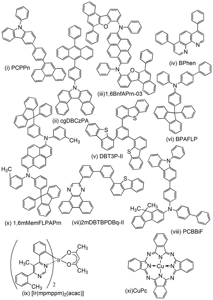
(发光元件1至发光元件3及比较发光元件1至比较发光元件3的制造方法)(Manufacturing method of light-emitting
首先,在玻璃衬底上利用溅射法形成银(Ag)、钯(Pd)及铜(Cu)的合金膜(简称:APC)来形成第一电极(反射电极)。第一电极的厚度为100nm,电极面积为2mm×2mm。First, an alloy film of silver (Ag), palladium (Pd) and copper (Cu) (abbreviation: APC) is formed on a glass substrate by sputtering to form a first electrode (reflective electrode). The thickness of the first electrode is 100 nm, and the electrode area is 2 mm×2 mm.
接着,在第一电极上作为透明导电膜利用溅射法形成包含氧化硅的铟锡氧化物。发光元件1的透明导电膜的厚度为30nm,发光元件2的透明导电膜的厚度为80nm,发光元件3的透明导电膜的厚度为30nm,比较发光元件1的透明导电膜的厚度为30nm,比较发光元件2的透明导电膜的厚度为60nm,比较发光元件3的透明导电膜的厚度为60nm。Next, indium tin oxide containing silicon oxide was formed as a transparent conductive film by sputtering on the first electrode. The thickness of the transparent conductive film of light-emitting
接着,作为形成有机化合物层的预处理,用水对形成有反射电极及透明导电膜的衬底的表面进行洗涤,以200℃焙烧1小时,然后进行UV臭氧处理370秒。Next, as a pretreatment for forming the organic compound layer, the surface of the substrate on which the reflective electrode and the transparent conductive film were formed was washed with water, baked at 200° C. for 1 hour, and then subjected to UV ozone treatment for 370 seconds.
然后,将衬底放入其内部被减压到10-4Pa左右的真空蒸镀装置中,并在真空蒸镀装置内的加热室中,以170℃进行30分钟的真空焙烧,然后对衬底进行30分钟左右的冷却。Then, put the substrate into a vacuum evaporation device whose interior is depressurized to about 10 -4 Pa, and carry out vacuum baking at 170° C. for 30 minutes in a heating chamber in the vacuum evaporation device, and then place the substrate on the substrate. Cool down for about 30 minutes.
接着,以形成有透明导电膜的面朝下方的方式将衬底固定于设置在真空蒸镀装置内的衬底支架上并将真空蒸镀装置减压到10-4Pa左右。然后,在透明导电膜上通过利用电阻加热的蒸镀法共蒸镀由上述结构式(i)表示的3-[4-(9-菲基)-苯基]-9-苯基-9H-咔唑(简称:PCPPn)和氧化钼(VI),由此形成第一空穴注入层。发光元件1的第一空穴注入层的厚度为60nm,发光元件2的第一空穴注入层的厚度为47.5nm,发光元件3的第一空穴注入层的厚度为40nm,比较发光元件1的第一空穴注入层的厚度为55nm,比较发光元件2的第一空穴注入层的厚度为70nm,比较发光元件3的第一空穴注入层的厚度为45nm。另外,将PCPPn与氧化钼的重量比调节为1:0.5(=PCPPn:氧化钼)。Next, the substrate was fixed on a substrate holder provided in the vacuum evaporation apparatus so that the surface on which the transparent conductive film was formed faced downward, and the vacuum evaporation apparatus was decompressed to about 10 −4 Pa. Then, 3-[4-(9-phenanthrenyl)-phenyl]-9-phenyl-9H-carboxylate represented by the above structural formula (i) was co-evaporated on the transparent conductive film by vapor deposition using resistance heating. azole (abbreviation: PCPPn) and molybdenum (VI) oxide, thereby forming the first hole injection layer. The thickness of the first hole injection layer of light-emitting
接着,在第一空穴注入层上以厚度为10nm的方式蒸镀PCPPn,来形成第一空穴传输层。Next, PCPPn was evaporated to a thickness of 10 nm on the first hole injection layer to form a first hole transport layer.
接着,在发光元件1至发光元件3中,在第一空穴传输层上以厚度为25nm的方式蒸镀由上述结构式(ii)表示的7-[4-(10-苯基-9-蒽基)苯基]-7H-二苯并[c,g]咔唑(简称:cgDBCzPA)和由上述结构式(iii)表示的N,N’-(芘-1,6-二基)双[(6,N-二苯基苯并[b]萘并[1,2-d]呋喃)-8-胺](简称:1,6BnfAPrn-03)并使其重量比为1:0.05(=cgDBCzPA:1,6BnfAPrn-03),由此形成第一发光层。Next, in the light-emitting
在比较发光元件1至比较发光元件3中,在第一空穴传输层上以厚度为25nm的方式蒸镀cgDBCzPA和由上述结构式(x)表示的N,N’-双(3-甲基苯基)-N,N’-双[3-(9-苯基-9H-芴-9-基)苯基]芘-1,6-二胺(简称:1,6mMemFLPAPrn)并使其重量比为1:0.05(=cgDBCzPA:1,6mMemFLPAPrn),由此形成第一发光层。In Comparative Light-Emitting
接着,在第一发光层上以厚度为5nm的方式蒸镀cgDBCzPA,并以厚度为15nm的方式蒸镀由上述结构式(iv)表示的红菲咯啉(简称:BPhen),由此形成第一电子传输层。Next, cgDBCzPA was vapor-deposited to a thickness of 5 nm on the first light-emitting layer, and bathophenanthroline (abbreviation: BPhen) represented by the above structural formula (iv) was vapor-deposited to a thickness of 15 nm, thereby forming the first electron transport layer.
在形成第一电子传输层之后,以厚度为0.1nm的方式蒸镀氧化锂(Li2O),然后以厚度为2nm的方式蒸镀由上述结构式(xi)表示的酞菁铜(简称:CuPc),而且共蒸镀由上述结构式(v)表示的4,4’,4”-(苯-1,3,5-三基)三(二苯并噻吩)(简称:DBT3P-II)和氧化钼(VI)并使其重量比为1:0.5(=DBT3P-II:氧化钼),由此形成中间层。中间层的厚度为12.5nm。After forming the first electron transport layer, lithium oxide (Li 2 O) was evaporated to a thickness of 0.1 nm, and copper phthalocyanine (abbreviation: CuPc) represented by the above structural formula (xi) was evaporated to a thickness of 2 nm. ), and co-evaporated 4,4',4"-(benzene-1,3,5-triyl) tri(dibenzothiophene) (abbreviation: DBT3P-II) represented by the above structural formula (v) and oxidation Molybdenum(VI) was added in a weight ratio of 1:0.5 (=DBT3P-II: molybdenum oxide), thereby forming an intermediate layer. The thickness of the intermediate layer was 12.5 nm.
然后,在中间层上以厚度为20nm的方式蒸镀由上述结构式(vi)表示的4-苯基-4’-(9-苯基芴-9-基)三苯胺(简称:BPAFLP),来形成第二空穴传输层。Then, 4-phenyl-4'-(9-phenylfluoren-9-yl)triphenylamine (abbreviation: BPAFLP) represented by the above structural formula (vi) was vapor-deposited on the intermediate layer to a thickness of 20 nm to A second hole transport layer is formed.
在形成第二空穴传输层之后,共蒸镀由上述结构式(vii)表示的2-[3’-(二苯并噻吩-4-基)联苯-3-基]二苯并[f,h]喹喔啉(简称:2mDBTBPDBq-II)、由上述结构式(viii)表示的N-(1,1’-联苯-4-基)-9,9-二甲基-N-[4-(9-苯基-9H-咔唑-3-基)苯基]-9H-芴-2-胺(简称:PCBBiF)以及由上述结构式(ix)表示的双{2-[5-甲基-6-(2-甲基苯基)-4-嘧啶基-κN3]苯基-κC}(2,4-戊二酮根-κ2O,O’)铱(III)(简称:[Ir(mpmppm)2(acac)])并使其重量比为0.8:0.2:0.06(=2mDBTBPDBq-II:PCBBiF:[Ir(mpmppm)2(acac)]),由此形成第二发光层。第二发光层的厚度为40nm。After forming the second hole transport layer, co-evaporation of 2-[3'-(dibenzothiophen-4-yl)biphenyl-3-yl]dibenzo[f, represented by the above structural formula (vii), h] quinoxaline (abbreviation: 2mDBTBPDBq-II), N-(1,1'-biphenyl-4-yl)-9,9-dimethyl-N-[4- (9-Phenyl-9H-carbazol-3-yl)phenyl]-9H-fluorene-2-amine (abbreviation: PCBBiF) and bis{2-[5-methyl- 6-(2-methylphenyl)-4-pyrimidinyl-κN3]phenyl-κC}(2,4-pentanedionato-κ 2 O, O') iridium (III) (abbreviation: [Ir( mmpmppm) 2 (acac)]) and made the weight ratio 0.8:0.2:0.06 (=2mDBTBPDBq-II:PCBBiF:[Ir(mpmppm) 2 (acac)]), thereby forming the second light-emitting layer. The thickness of the second light-emitting layer was 40 nm.
接着,在第二发光层上以厚度为15nm的方式蒸镀2mDBTBPDBq-II,然后,在发光元件1至3中以厚度为20nm的方式蒸镀BPhen,而在比较发光元件1至3中以厚度为15nm的方式蒸镀BPhen,由此形成第二电子传输层。Next, 2mDBTBPDBq-II was vapor-deposited to a thickness of 15 nm on the second light-emitting layer, and then BPhen was vapor-deposited to a thickness of 20 nm in the light-emitting
之后,以厚度为1nm的方式蒸镀氟化锂来形成电子注入层,最后以厚度为15nm的方式共蒸镀银和镁并使其体积比为1:0.1,接着利用溅射法形成70nm的ITO,来形成第二电极(半透射半反射电极),由此形成发光元件1至发光元件3及比较发光元件1至比较发光元件3。在上述蒸镀过程中,都利用电阻加热法进行蒸镀。After that, lithium fluoride was vapor-deposited to a thickness of 1nm to form an electron injection layer, and finally silver and magnesium were co-deposited to a thickness of 15nm so that the volume ratio was 1:0.1, and then a 70nm layer was formed by sputtering. ITO, to form the second electrode (semi-transmissive and semi-reflective electrode), thereby forming the light-emitting
表1示出发光元件1至发光元件3及比较发光元件1至比较发光元件3的元件结构。Table 1 shows the element structures of Light-emitting
[表1][Table 1]

后面接*6→followed by *6→
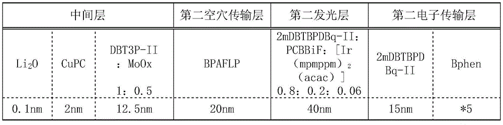
*6后面接*7→*6 followed by *7→
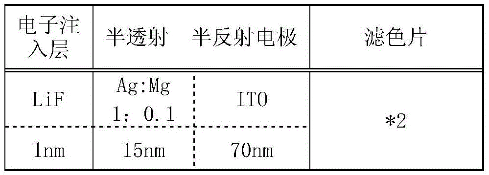
*7*7
*1发光元件1至发光元件3:1,6BnfAPrn-03*1 Light-emitting
比较发光元件1至比较发光元件3:1,6mMemFLPAPrnComparative Light-Emitting
*2发光元件1及比较发光元件1:0.8μm*2 Light-emitting
发光元件2及比较发光元件2:蓝色0.8μmLight-emitting
发光元件3:绿色1.3μm,比较发光元件3:红色2.4μmLight-emitting element 3: Green 1.3 μm, Comparative light-emitting element 3: Red 2.4 μm
*3发光元件1:30nm,发光元件2:80nm,发光元件3:30nm*3 light emitting element 1: 30nm, light emitting element 2: 80nm, light emitting element 3: 30nm
比较发光元件1:30nm,比较发光元件2:60nm,比较发光元件3:60nmComparative light-emitting element 1: 30nm, Comparative light-emitting element 2: 60nm, Comparative light-emitting element 3: 60nm
*4发光元件1:60nm,发光元件2:47.5nm,发光元件3:40nm*4 light emitting element 1: 60nm, light emitting element 2: 47.5nm, light emitting element 3: 40nm
比较发光元件1:55nm,比较发光元件2:70nm,比较发光元件3:45nmComparative light-emitting element 1: 55nm, Comparative light-emitting element 2: 70nm, Comparative light-emitting element 3: 45nm
*5发光元件1至发光元件3:20nm*5
比较发光元件1至比较发光元件3:15nmComparative Light-Emitting
在氮气氛的手套箱中,以不使发光元件暴露于大气的方式使用玻璃衬底对发光元件1至发光元件3及比较发光元件1至比较发光元件3进行密封(将密封剂涂敷在元件的周围,在密封时进行UV处理(波长为365nm,6J/cm2)以及80℃的温度下的1小时的热处理),然后测定初期特性。该测定在室温下(在保持为25℃的气氛中)进行。Light-emitting
图16示出发光元件1至发光元件3的亮度-电流密度特性,图17示出电流效率-亮度特性,图18示出亮度-电压特性,图19示出电流-电压特性,图20示出色度坐标。16 shows the luminance-current density characteristics of light-emitting
另外,图21示出比较发光元件1至比较发光元件3的亮度-电流密度特性,图22示出电流效率-亮度特性,图23示出亮度-电压特性,图24示出电流-电压特性,图25示出色度坐标。In addition, FIG. 21 shows luminance-current density characteristics of comparative light-emitting
如图20及图25所示,使用1,6BnfAPrn-03的发光元件2的1000cd/m2附近的色度为(0.152,0.037),而使用1,6mMemFLPAPrn的比较发光元件2的色度为(0.160,0.087),由此可知发光元件2呈现更深的蓝色发光。As shown in FIG. 20 and FIG. 25, the chromaticity of the light-emitting
在此,图26示出1,6BnfAPrn-03的甲苯溶液中的发射光谱。从图26可知,1,6BnfAPrn-03的甲苯溶液中的发射光谱的峰值波长为450nm。该光谱的半宽为40nm。另一方面,用于比较发光元件的1,6mMemFLPAPrn的甲苯溶液中的发射光谱的峰值波长为461nm。Here, FIG. 26 shows the emission spectrum of 1,6BnfAPrn-03 in a toluene solution. As can be seen from FIG. 26 , the peak wavelength of the emission spectrum in the toluene solution of 1,6BnfAPrn-03 is 450 nm. The half width of this spectrum is 40 nm. On the other hand, the peak wavelength of the emission spectrum in the toluene solution of 1,6 mMemFLPAPrn used for the comparison light-emitting element was 461 nm.
接着,估算使用这些元件制造的发光装置进行D65附近的白色显示时的功耗。在以下条件下估算发光装置的功耗。Next, power consumption was estimated when a light-emitting device manufactured using these elements performed white display around D65. The power consumption of the light emitting device was estimated under the following conditions.
[表2][Table 2]
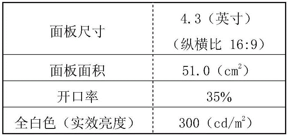
表3示出实施例的发光装置的计算结果,表4示出比较例子的发光装置的计算结果。Table 3 shows the calculation results of the light emitting device of the example, and Table 4 shows the calculation results of the light emitting device of the comparative example.
[表3][table 3]
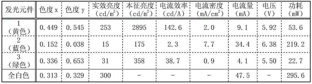
[表4][Table 4]
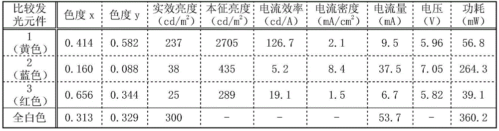
在上述计算结果中,实效亮度为本征亮度×开口率×1/4(子像素的面积比率(假设一个像素由红色、绿色、蓝色及黄色的四个子像素构成的发光装置)),电流量为电流密度×面板面积×开口率×1/4(各子像素的面积比率),显示部的功耗为电流量×电压。In the above calculation results, the effective luminance is intrinsic luminance × aperture ratio × 1/4 (area ratio of sub-pixels (assuming a light-emitting device consisting of four sub-pixels of red, green, blue, and yellow)). The flow rate is current density×panel area×aperture ratio×1/4 (area ratio of each sub-pixel), and the power consumption of the display unit is current amount×voltage.
从表3和表4可知,比较例子的发光装置的为了获得D65附近的白色发光而需要的蓝色发光(比较发光元件2的发光)的亮度为38cd/m2,而实施例的发光装置中的该亮度更低,为15cd/m2。这是因为:由于作为蓝色发光材料使用实施方式1及实施方式2所示的荧光发光物质1,6BnfAPrn-03,所以蓝色的色度得到改善而降低为了获得白色发光而需要的蓝色发光的实效亮度。为了获得白色发光而需要的发光元件2的功耗也随之大幅度地降低。From Table 3 and Table 4, it can be seen that the luminance of the blue light emission (light emission of comparative light-emitting element 2) required to obtain white light emission near D65 in the light-emitting device of the comparative example is 38 cd/m 2 , while that of the light-emitting device of the embodiment The luminance is lower at 15 cd/m 2 . This is because the blue chromaticity is improved and the blue luminescence required to obtain white luminescence is reduced by using the fluorescent
为了获得D65附近的白色发光而需要的比较发光元件3的功耗为39.1mW,而发光元件3的功耗为22.7mW,这也表明该实施例的发光装置的功耗更低。The power consumption of comparative light-emitting element 3 required to obtain white light near D65 is 39.1 mW, while the power consumption of light-emitting element 3 is 22.7 mW, which also shows that the light-emitting device of this embodiment has lower power consumption.
这是因为:由于发光元件2发射深蓝色的发光,因此通过组合该蓝色发光与发光元件1的黄色发光而获得的发光的色调发生变化,而改变为了获得D65附近的白色发光而需要的第三发光的颜色。在实施例的发光装置中,作为第三发光需要绿色发光,而在比较例子的发光装置中作为第三发光需要红色发光。实施例的发光装置的为了获得白色发光而需要的绿色发光的亮度的比率比比较例子的发光装置中的红色发光的亮度的比率高。This is because the color tone of the light emission obtained by combining the blue light emission with the yellow light emission of the light-emitting
然而,绿色发光的视见函数比红色发光良好,因此发光元件3(绿色发光元件)的电流效率大约为比较发光元件3(红色发光元件)的两倍。因此,在实施例的发光装置中,即使为了获得白色发光而需要的第三发光(发光元件3的发光)的亮度的比率增加,也能够使发光元件3的功耗比比较发光元件3低。However, the viewing function of the green light emission is better than that of the red light emission, so the current efficiency of the light emitting element 3 (green light emitting element) is about twice that of the comparative light emitting element 3 (red light emitting element). Therefore, in the light-emitting device of the example, even if the ratio of the luminance of the third light emission (light emission of the light-emitting element 3 ) required to obtain white light emission is increased, the power consumption of the light-emitting element 3 can be made lower than that of the comparative light-emitting element 3 .
在实施例的发光元件中,虽然为了获得300cd/m2的D65附近的白色发光而需要的发光元件2(蓝色)和发光元件3(绿色)的实效亮度都比比较例子的发光元件中的比较发光元件2(蓝色)和比较发光元件3(红色)的实效亮度低,但是,通过增加发光元件1的黄色发光的亮度来补充上述亮度下降。由于发光元件1(黄色发光元件)的电流效率非常高,所以发光元件2和发光元件3所需要的亮度的下降带来的功耗抵消发光元件1所需要的亮度的上升造成的功耗,所以可以实现实施例的发光装置的低功耗化。In the light-emitting element of the example, although the effective luminance of the light-emitting element 2 (blue) and the light-emitting element 3 (green), which are required to obtain white light emission near D65 of 300 cd/m 2 , are both higher than those of the light-emitting element of the comparative example. The effective luminance of comparative light-emitting element 2 (blue) and comparative light-emitting element 3 (red) is low, but the above-mentioned decrease in luminance is compensated by increasing the luminance of yellow light emitted by light-emitting
其结果,进行白色显示时的实施例的发光装置的不包含驱动FET时的功耗为5.8mW/cm2,包含驱动FET时的功耗为14mW/cm2。比较例子的发光装置的不包含驱动FET时的功耗为7.1mW/cm2,包含驱动FET时的功耗为16mW/cm2,因此可以使功耗降低一成至两成左右。注意,包含驱动FET时的功耗通过假设阳极与阴极之间的电压(发光元件部与驱动FET部的总电压值)都是15V的情况而估算。As a result, the power consumption of the light-emitting device of the example when performing white display was 5.8 mW/cm 2 when not including the driving FET, and was 14 mW/cm 2 when including the driving FET. The power consumption of the light-emitting device of the comparative example is 7.1 mW/cm 2 without driving FET and 16 mW/cm 2 including driving FET, so the power consumption can be reduced by about 10 to 20 percent. Note that including the power consumption when driving the FET, it is estimated by assuming that the voltage between the anode and the cathode (the total voltage value of the light emitting element part and the driving FET part) is 15V.
蓝色发光元件的功耗比其他颜色的发光元件大得多,因此色度变化所带来的功耗下降的效果较高。另外,为了获得D65附近的白色发光而需要的发光颜色及其亮度比率的平衡的变化也带来低功耗化,因此使用实施方式1所示的荧光发光物质的实施例的发光装置能够实现低功耗化。The power consumption of the blue light-emitting element is much larger than that of other color light-emitting elements, so the power consumption reduction effect brought about by the chromaticity change is relatively high. In addition, changes in the balance between the emission color and its luminance ratio required to obtain white emission near D65 also lead to low power consumption, so the light-emitting device of the example using the fluorescent light-emitting substance shown in
实施例2Example 2
在本实施例中,使用构成本发明的发光装置的发光元件(红色发光元件(发光元件4)、黄色发光元件(发光元件5)、绿色发光元件(发光元件6)及蓝色发光元件(发光元件7))及构成比较发光装置的发光元件(红色发光元件(比较发光元件4)、绿色发光元件(比较发光元件5)及蓝色发光元件(比较发光元件6))估算各发光装置进行白色显示时的功耗,并说明其结果。In this embodiment, the light-emitting elements (red light-emitting element (light-emitting element 4), yellow light-emitting element (light-emitting element 5), green light-emitting element (light-emitting element 6), and blue light-emitting element (light-emitting element 6) constituting the light-emitting device of the present invention are used. Element 7)) and the light-emitting elements (red light-emitting element (comparative light-emitting element 4), green light-emitting element (comparative light-emitting element 5) and blue light-emitting element (comparative light-emitting element 6)) that constitute the comparative light-emitting device power consumption when displayed, and explain the results.
以下示出用于发光元件4至发光元件7及比较发光元件4至比较发光元件6的有机化合物的结构式。Structural formulas of organic compounds used in Light-emitting

(发光元件4至发光元件7及比较发光元件4至比较发光元件6的制造方法)(Manufacturing methods of light-emitting
首先,在玻璃衬底上利用溅射法形成银(Ag)、钯(Pd)及铜(Cu)的合金膜(简称:APC)来形成第一电极(反射电极)。第一电极的厚度为100nm,电极面积为2mm×2mm。First, an alloy film of silver (Ag), palladium (Pd) and copper (Cu) (abbreviation: APC) is formed on a glass substrate by sputtering to form a first electrode (reflective electrode). The thickness of the first electrode is 100 nm, and the electrode area is 2 mm×2 mm.
接着,在第一电极上作为透明导电膜利用溅射法形成包含氧化硅的铟锡氧化物。发光元件4(红色)的透明导电膜的厚度为80nm,发光元件5(黄色)的透明导电膜的厚度为45nm,发光元件6(绿色)的透明导电膜的厚度为45nm,发光元件7(蓝色)的透明导电膜的厚度为80nm,比较发光元件4(红色)的透明导电膜的厚度为85nm,比较发光元件5(绿色)的透明导电膜的厚度为45nm,比较发光元件6(蓝色)的透明导电膜的厚度为110nm。Next, indium tin oxide containing silicon oxide was formed as a transparent conductive film by sputtering on the first electrode. The thickness of the transparent conductive film of light-emitting element 4 (red) is 80nm, the thickness of the transparent conductive film of light-emitting element 5 (yellow) is 45nm, the thickness of the transparent conductive film of light-emitting element 6 (green) is 45nm, and the thickness of light-emitting element 7 (blue) The thickness of the transparent conductive film of color) is 80nm, the thickness of the transparent conductive film of comparative light-emitting element 4 (red) is 85nm, the thickness of the transparent conductive film of comparative light-emitting element 5 (green) is 45nm, and the thickness of comparative light-emitting element 6 (blue) ) The thickness of the transparent conductive film is 110nm.
接着,作为形成有机化合物层的预处理,用水对形成有反射电极及透明导电膜的衬底的表面进行洗涤,以200℃焙烧1小时,然后进行UV臭氧处理370秒。Next, as a pretreatment for forming the organic compound layer, the surface of the substrate on which the reflective electrode and the transparent conductive film were formed was washed with water, baked at 200° C. for 1 hour, and then subjected to UV ozone treatment for 370 seconds.
然后,将衬底放入其内部被减压到10-4Pa左右的真空蒸镀装置中,并在真空蒸镀装置内的加热室中,以170℃进行30分钟的真空焙烧,然后对衬底进行30分钟左右的冷却。Then, put the substrate into a vacuum evaporation device whose interior is depressurized to about 10 -4 Pa, and carry out vacuum baking at 170° C. for 30 minutes in a heating chamber in the vacuum evaporation device, and then place the substrate on the substrate. Cool down for about 30 minutes.
接着,以形成有透明导电膜的面朝下方的方式将衬底固定于设置在真空蒸镀装置内的衬底支架上并将真空蒸镀装置减压到10-4Pa左右。然后,在透明导电膜上通过利用电阻加热的蒸镀法共蒸镀由上述结构式(i)表示的3-[4-(9-菲基)-苯基]-9-苯基-9H-咔唑(简称:PCPPn)和氧化钼(VI),由此形成第一空穴注入层。发光元件4(红色)的第一空穴注入层的厚度为30nm,发光元件5(黄色)的第一空穴注入层的厚度为40nm,发光元件6(绿色)的第一空穴注入层的厚度为22.5nm,发光元件7(蓝色)的第一空穴注入层的厚度为50nm,比较发光元件4(红色)的第一空穴注入层的厚度为10nm,比较发光元件5(绿色)的第一空穴注入层的厚度为10nm,比较发光元件6(蓝色)的第一空穴注入层的厚度为15nm。另外,将PCPPn与氧化钼的重量比调节为1:0.5(=PCPPn:氧化钼)。Next, the substrate was fixed on a substrate holder provided in the vacuum evaporation apparatus so that the surface on which the transparent conductive film was formed faced downward, and the vacuum evaporation apparatus was decompressed to about 10 −4 Pa. Then, 3-[4-(9-phenanthrenyl)-phenyl]-9-phenyl-9H-carboxylate represented by the above structural formula (i) was co-evaporated on the transparent conductive film by vapor deposition using resistance heating. azole (abbreviation: PCPPn) and molybdenum (VI) oxide, thereby forming the first hole injection layer. The thickness of the first hole injection layer of light emitting element 4 (red) is 30nm, the thickness of the first hole injection layer of light emitting element 5 (yellow) is 40nm, the thickness of the first hole injection layer of light emitting element 6 (green) The thickness is 22.5nm, the thickness of the first hole injection layer of light-emitting element 7 (blue) is 50nm, the thickness of the first hole injection layer of comparative light-emitting element 4 (red) is 10nm, and the thickness of comparative light-emitting element 5 (green) The thickness of the first hole injection layer of 10 nm was 10 nm, and the thickness of the first hole injection layer of comparative light-emitting element 6 (blue) was 15 nm. In addition, the weight ratio of PCPPn to molybdenum oxide was adjusted to 1:0.5 (=PCPPn:molybdenum oxide).
接着,在第一空穴注入层上在发光元件4至发光元件7中以厚度为10nm的方式蒸镀PCPPn,而在比较发光元件4至比较发光元件6中以厚度为15nm的方式蒸镀PCPPn,来形成第一空穴传输层。Next, on the first hole injection layer, PCPPn was vapor-deposited in a thickness of 10 nm in Light-emitting
接着,在第一空穴传输层上以厚度为25nm的方式蒸镀由上述结构式(ii)表示的7-[4-(10-苯基-9-蒽基)苯基]-7H-二苯并[c,g]咔唑(简称:cgDBCzPA)和由上述结构式(iii)表示的N,N’-(芘-1,6-二基)双[(6,N-二苯基苯并[b]萘并[1,2-d]呋喃)-8-胺](简称:1,6BnfAPrn-03)并使其重量比为1:0.05(=cgDBCzPA:1,6BnfAPrn-03),由此形成第一发光层。Next, 7-[4-(10-phenyl-9-anthracenyl)phenyl]-7H-diphenylene represented by the above structural formula (ii) was vapor-deposited on the first hole transport layer to a thickness of 25 nm. And[c,g]carbazole (abbreviation: cgDBCzPA) and N,N'-(pyrene-1,6-diyl)bis[(6,N-diphenylbenzo[ b] Naphtho[1,2-d]furan)-8-amine] (abbreviation: 1,6BnfAPrn-03) and make it a weight ratio of 1:0.05 (=cgDBCzPA:1,6BnfAPrn-03), thus forming the first luminescent layer.
接着,在第一发光层上以厚度为5nm的方式蒸镀cgDBCzPA,并以厚度为15nm的方式蒸镀由上述结构式(iv)表示的红菲咯啉(简称:BPhen),由此形成第一电子传输层。Next, cgDBCzPA was vapor-deposited to a thickness of 5 nm on the first light-emitting layer, and bathophenanthroline (abbreviation: BPhen) represented by the above structural formula (iv) was vapor-deposited to a thickness of 15 nm, thereby forming the first electron transport layer.
在形成第一电子传输层之后,以厚度为0.1nm的方式蒸镀氧化锂(Li2O),然后以厚度为2nm的方式蒸镀由上述结构式(xi)表示的酞菁铜(简称:CuPc),而且共蒸镀由上述结构式(v)表示的4,4’,4”-(苯-1,3,5-三基)三(二苯并噻吩)(简称:DBT3P-II)和氧化钼并使其重量比为1:0.5(=DBT3P-II:氧化钼),由此形成中间层。中间层的厚度为12.5nm。After forming the first electron transport layer, lithium oxide (Li 2 O) was evaporated to a thickness of 0.1 nm, and copper phthalocyanine (abbreviation: CuPc) represented by the above structural formula (xi) was evaporated to a thickness of 2 nm. ), and co-evaporated 4,4',4"-(benzene-1,3,5-triyl) tri(dibenzothiophene) (abbreviation: DBT3P-II) represented by the above structural formula (v) and oxidation Molybdenum was added in a weight ratio of 1:0.5 (=DBT3P-II: molybdenum oxide), thereby forming an intermediate layer. The thickness of the intermediate layer was 12.5 nm.
然后,在中间层上以厚度为20nm的方式蒸镀由上述结构式(vi)表示的4-苯基-4’-(9-苯基芴-9-基)三苯胺(简称:BPAFLP),来形成第二空穴传输层。Then, 4-phenyl-4'-(9-phenylfluoren-9-yl)triphenylamine (abbreviation: BPAFLP) represented by the above structural formula (vi) was vapor-deposited on the intermediate layer to a thickness of 20 nm to A second hole transport layer is formed.
在形成第二空穴传输层之后,在发光元件4至发光元件7中,共蒸镀由上述结构式(vii)表示的2-[3’-(二苯并噻吩-4-基)联苯-3-基]二苯并[f,h]喹喔啉(简称:2mDBTBPDBq-II)、由上述结构式(viii)表示的N-(1,1’-联苯-4-基)-9,9-二甲基-N-[4-(9-苯基-9H-咔唑-3-基)苯基]-9H-芴-2-胺(简称:PCBBiF)以及由上述结构式(ix)表示的双{2-[5-甲基-6-(2-甲基苯基)-4-嘧啶基-κN3]苯基-κC}(2,4-戊二酮根-κ2O,O’)铱(III)(简称:[Ir(mpmppm)2(acac)])并使其重量比为0.8:0.2:0.06(=2mDBTBPDBq-II:PCBBiF:[Ir(mpmppm)2(acac)]),由此形成第二发光层。第二发光层的厚度为40nm。After forming the second hole transport layer, in the light-emitting
在比较发光元件4至比较发光元件6中,在形成第二空穴传输层之后,以厚度为20nm的方式共蒸镀2mDBTBPDBq-II、PCBBiF以及由上述结构式(xii)表示的双[2-(6-tert-丁基-4-嘧啶基-κN3)苯基-κC](2,4-戊二酮根-κ2O,O’)铱(III)(简称:[Ir(tBuppm)2(acac)])并使其重量比为0.7:0.3:0.06(=2mDBTBPDBq-II:PCBBiF:[Ir(tBuppm)2(acac)]),然后以厚度为20nm的方式共蒸镀2mDBTBPDBq-II和由上述结构式(xiii)表示的双{4,6-二甲基-2-[5-(2,6-二甲基苯基)-3-(3,5-二甲基苯基)-2-吡嗪基-κN]苯基-κC}(2,8-二甲基-4,6-壬二酮根-κ2O,O’)铱(III)(简称:[Ir(dmdppr-dmp)2(divm)])并使其重量比为1:0.06(=2mDBTBPDBq-II:[Ir(dmdppr-dmp)2(divm)]),由此形成第二发光层。In Comparative Light-Emitting
接着,在第二发光层上,在发光元件4至发光元件7中以厚度为15nm的方式蒸镀2mDBTBPDBq-II,而在比较发光元件4至比较发光元件6中以厚度为30nm的方式蒸镀2mDBTBPDBq-II,并且,在2mDBTBPDBq-II上,在发光元件4至发光元件7中以厚度为20nm的方式蒸镀BPhen,而在比较发光元件4至比较发光元件6中以厚度为15nm的方式蒸镀BPhen,由此形成第二电子传输层。Next, on the second light-emitting layer, 2 mDBTBPDBq-II was vapor-deposited in a thickness of 15 nm in Light-emitting
之后,以厚度为1nm的方式蒸镀氟化锂来形成电子注入层,最后以厚度为15nm的方式共蒸镀银和镁并使其体积比为1:0.1,接着利用溅射法形成70nm的ITO,来形成第二电极(半透射半反射电极),由此形成发光元件4至发光元件7及比较发光元件4至比较发光元件6。在上述蒸镀过程中,都利用电阻加热法进行蒸镀。After that, lithium fluoride was vapor-deposited to a thickness of 1nm to form an electron injection layer, and finally silver and magnesium were co-deposited to a thickness of 15nm so that the volume ratio was 1:0.1, and then a 70nm layer was formed by sputtering. ITO, to form the second electrode (semi-transmissive and semi-reflective electrode), thereby forming the light-emitting
表5示出发光元件4至发光元件7及比较发光元件4至比较发光元件6的元件结构。Table 5 shows the element structures of Light-emitting
[表5][table 5]
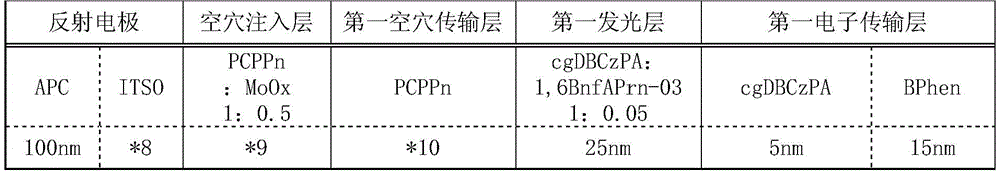
后面接*15→ followed by *15→
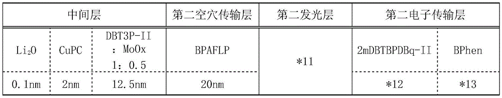
*15 后面接*16→*15 followed by *16→
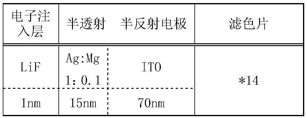
*16*16
*8发光元件4:80nm,发光元件5:45nm,发光元件6:45nm,发光元件7:80nm*8 Light emitting element 4: 80nm, Light emitting element 5: 45nm, Light emitting element 6: 45nm, Light emitting element 7: 80nm
比较发光元件4:85nm,比较发光元件5:45nm,比较发光元件6:110nmComparative light-emitting element 4: 85nm, Comparative light-emitting element 5: 45nm, Comparative light-emitting element 6: 110nm
*9发光元件4:30nm,发光元件5:40nm,发光元件6:22.5nm,发光元件7:50nm*9 Light emitting element 4: 30nm, Light emitting element 5: 40nm, Light emitting element 6: 22.5nm, Light emitting element 7: 50nm
比较发光元件4:10nm,比较发光元件5:10nm,比较发光元件6:15nmComparative light-emitting element 4: 10nm, Comparative light-emitting element 5: 10nm, Comparative light-emitting element 6: 15nm
*10发光元件4至发光元件7:10nm,比较发光元件4至比较发光元件6:15nm*10 Light-emitting
*11发光元件4至发光元件7*11 Light-emitting
2mDBTBPDBq-II:PCBBiF:[Ir(mpmppm)2(acac)]=0.8:0.2:0.06,40nm2mDBTBPDBq-II: PCBBiF: [Ir(mpmppm) 2 (acac)]=0.8:0.2:0.06,40nm
比较发光元件4至比较发光元件6Comparative Light-Emitting
2mDBTBPDBq-II:PCBBiF:[Ir(tBuppm)2(acac)]=0.7:0.3:0.06,20nm2mDBTBPDBq-II: PCBBiF: [Ir(tBuppm) 2 (acac)]=0.7:0.3:0.06, 20nm
+2mDBTBPDBq-II:[Ir(dmdppr-dmp)2(divm)]=1:0.06,20nm+2mDBTBPDBq-II:[Ir(dmdppr-dmp) 2 (divm)]=1:0.06,20nm
*12发光元件4至发光元件7:15nm,比较发光元件4至比较发光元件6:30nm*12 Light-emitting
*13发光元件4至发光元件7:20nm,比较发光元件4至比较发光元件6:15nm*13 Light-emitting
*14发光元件4及比较发光元件4:红色2.4μm*14 Light-emitting
发光元件5:黄色0.8μmLight emitting element 5: yellow 0.8μm
发光元件6及比较发光元件5:绿色1.3μmLight-emitting
发光元件7及比较发光元件6:蓝色0.8μmLight-emitting element 7 and comparative light-emitting element 6: blue 0.8 μm
在氮气氛的手套箱中,以不使发光元件暴露于大气的方式使用玻璃衬底对发光元件4至发光元件7及比较发光元件4至比较发光元件6进行密封(将密封剂涂敷在元件的周围,在密封时进行UV处理(波长为365nm,6J/cm2)以及80℃的温度下的1小时的热处理),然后测定初期特性。该测定在室温下(在保持为25℃的气氛中)进行。Light-emitting
图28示出发光元件4至发光元件7的亮度-电流密度特性,图29示出电流效率-亮度特性,图30示出亮度-电压特性,图31示出电流-电压特性,图32示出色度坐标。28 shows the luminance-current density characteristics of the light-emitting
另外,图33示出比较发光元件4至比较发光元件6的亮度-电流密度特性,图34示出电流效率-亮度特性,图35示出亮度-电压特性,图36示出电流-电压特性。33 shows the luminance-current density characteristics of Comparative Light-emitting
接着,估算使用这些元件制造的发光装置进行D65附近的白色显示时的功耗。在以下的条件下,估算发光装置的功耗。Next, power consumption was estimated when a light-emitting device manufactured using these elements performed white display around D65. Under the following conditions, the power consumption of the light emitting device was estimated.
[表6][Table 6]
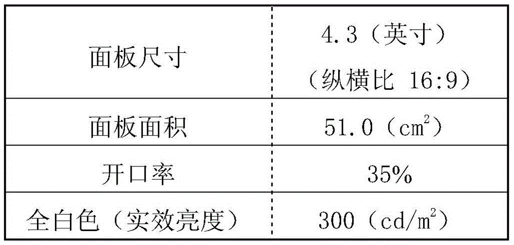
表7示出实施例的发光装置的计算结果,表8示出比较例子的发光装置的计算结果。Table 7 shows the calculation results of the light emitting device of the example, and Table 8 shows the calculation results of the light emitting device of the comparative example.
[表7][Table 7]
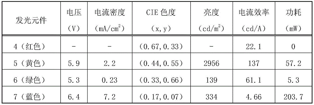
[表8][Table 8]
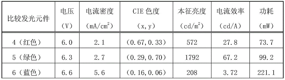
在上述计算结果中,实效亮度为本征亮度×开口率×1/4(子像素的面积比率(假设一个像素由红色、绿色、蓝色及黄色的四个子像素构成的发光装置)),电流量为电流密度×面板面积×开口率×1/4(各子像素的面积比率),显示部的功耗为电流量×电压。In the above calculation results, the effective luminance is intrinsic luminance × aperture ratio × 1/4 (area ratio of sub-pixels (assuming a light-emitting device consisting of four sub-pixels of red, green, blue, and yellow)). The flow rate is current density×panel area×aperture ratio×1/4 (area ratio of each sub-pixel), and the power consumption of the display unit is current amount×voltage.
从表7和表8可知,为了发射白色发光而需要的功耗在比较例子的发光装置中为394mW,而在实施例的发光装置中为266mW,实施例的发光装置的功耗更低。当在比较例子的发光装置中获得白色发光时,比较发光元件4(红色)及比较发光元件5(绿色)都需要规定比率的本征亮度。然而,当在实施例的发光装置中获得白色发光时,发光元件4(红色)处于非发光状态,发光元件6(绿色)的发光亮度也低,为139cd/m2,几乎不影响到功耗。换而言之,当在实施例的发光装置中获得白色发光时,几乎仅使发光元件7(蓝色)及发光元件5(黄色)发光。由于发光元件5(黄色)的电流效率高,为137cd/A,因此虽然比较例子的发光装置和实施例的发光装置的蓝色元件的功耗大致相同,但是实施例的发光装置的功耗比比较例子的发光装置低得多。It can be seen from Table 7 and Table 8 that the power consumption required to emit white light is 394 mW in the light emitting device of the comparative example, and 266 mW in the light emitting device of the embodiment, and the power consumption of the light emitting device of the embodiment is lower. In order to obtain white light emission in the light-emitting device of the comparative example, both the comparative light-emitting element 4 (red) and the comparative light-emitting element 5 (green) require a predetermined ratio of intrinsic luminance. However, when white light emission is obtained in the light-emitting device of the embodiment, the light-emitting element 4 (red) is in a non-light-emitting state, and the light-emitting brightness of the light-emitting element 6 (green) is also low at 139 cd/m 2 , which hardly affects power consumption. . In other words, when white light emission is obtained in the light emitting device of the example, almost only light emitting element 7 (blue) and light emitting element 5 (yellow) are made to emit light. Since the current efficiency of the light-emitting element 5 (yellow) is high at 137 cd/A, although the power consumption of the blue element of the light-emitting device of the comparative example and the light-emitting device of the embodiment is approximately the same, the power consumption of the light-emitting device of the embodiment is lower than The light emitting device of the comparative example is much lower.
实施例3Example 3
示出估算本发明的一个方式的发光装置以300cd/m2进行D65附近的白色显示时的亮度劣化的结果。在本实施例中,对具有与本发明的一个方式的发光装置中的发光元件相同结构的发光元件8(蓝色)及发光元件9(黄色)进行驱动试验,其中,在电流密度为恒定且初始亮度分别为300cd/m2和3000cd/m2。将各发光元件的初始亮度设定为接近于在具有如下条件的本发明的一个方式的发光装置中为了获得D65附近的白色显示而需要的亮度的值。假设进行白色显示的情况进行驱动试验是因为需要一直发射光的白色显示是劣化速度最快的条件。The result of estimating luminance degradation when a light-emitting device according to one embodiment of the present invention performs white display near D65 at 300 cd/m 2 is shown. In this example, a driving test was performed on the light-emitting element 8 (blue) and the light-emitting element 9 (yellow) having the same structure as the light-emitting element in the light-emitting device according to one embodiment of the present invention. The initial luminances were 300cd/m 2 and 3000cd/m 2 , respectively. The initial luminance of each light emitting element is set to a value close to the luminance required to obtain a white display near D65 in the light emitting device according to one embodiment of the present invention having the following conditions. The driving test was performed assuming that a white display is performed because a white display that requires constant light emission is the condition with the fastest degradation rate.
[表9][Table 9]

注意,由于如下两个理由,不对红色发光元件及绿色发光元件进行测定:由于从黄色发光层提取光,因此可认为红色发光元件及绿色发光元件的劣化举动与黄色发光元件相同;如实施例2所示,在进行显示D65附近的白色显示时红色发光元件及绿色发光元件所需要的亮度较小,而不对可靠性造成影响。Note that the red light-emitting element and the green light-emitting element were not measured for the following two reasons: Since light is extracted from the yellow light-emitting layer, it can be considered that the degradation behavior of the red light-emitting element and the green light-emitting element is the same as that of the yellow light-emitting element; as in Example 2 As shown, the luminance required for the red light-emitting element and the green light-emitting element is relatively small when performing white display near the display D65, and the reliability is not affected.
以下示出用于发光元件8及发光元件9的有机化合物的结构式。Structural formulas of organic compounds used for the light-emitting
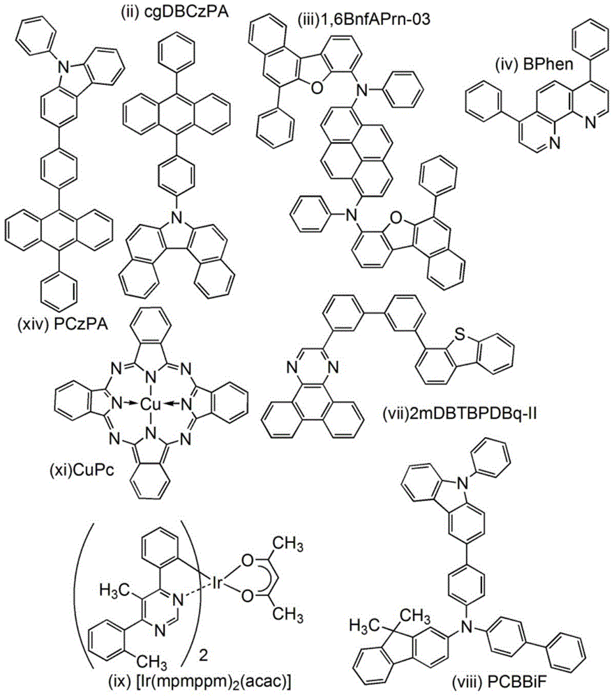
(发光元件8及发光元件9的制造方法)(Methods of Manufacturing Light-Emitting
首先,在玻璃衬底上利用溅射法形成银(Ag)、钯(Pd)及铜(Cu)的合金膜(简称:APC)来形成第一电极(反射电极)。第一电极的厚度为100nm,电极面积为2mm×2mm。First, an alloy film of silver (Ag), palladium (Pd) and copper (Cu) (abbreviation: APC) is formed on a glass substrate by sputtering to form a first electrode (reflective electrode). The thickness of the first electrode is 100 nm, and the electrode area is 2 mm×2 mm.
接着,在第一电极上作为透明导电膜利用溅射法形成包含氧化硅的铟锡氧化物。发光元件8(蓝色)的透明导电膜的厚度为85nm,发光元件9(黄色)的透明导电膜的厚度为65nm。Next, indium tin oxide containing silicon oxide was formed as a transparent conductive film by sputtering on the first electrode. The thickness of the transparent conductive film of the light-emitting element 8 (blue) was 85 nm, and the thickness of the transparent conductive film of the light-emitting element 9 (yellow) was 65 nm.
接着,作为形成有机化合物层的预处理,用水对形成有反射电极及透明导电膜的衬底的表面进行洗涤,以200℃焙烧1小时,然后进行UV臭氧处理370秒。Next, as a pretreatment for forming the organic compound layer, the surface of the substrate on which the reflective electrode and the transparent conductive film were formed was washed with water, baked at 200° C. for 1 hour, and then subjected to UV ozone treatment for 370 seconds.
然后,将衬底放入其内部被减压到10-4Pa左右的真空蒸镀装置中,并在真空蒸镀装置内的加热室中,以170℃进行30分钟的真空焙烧,然后对衬底进行30分钟左右的冷却。Then, put the substrate into a vacuum evaporation device whose interior is depressurized to about 10 -4 Pa, and carry out vacuum baking at 170° C. for 30 minutes in a heating chamber in the vacuum evaporation device, and then place the substrate on the substrate. Cool down for about 30 minutes.
接着,以形成有透明导电膜的面朝下方的方式将衬底固定于设置在真空蒸镀装置内的衬底支架上。然后,在透明导电膜上通过利用电阻加热的蒸镀法共蒸镀由上述结构式(xiv)表示的9-苯基-3-[4-(10-苯基-9-蒽基)苯基]-9H-咔唑(简称:PCzPA)和氧化钼(VI),由此形成第一空穴注入层。发光元件8(蓝色)的第一空穴注入层的厚度为40nm,发光元件9(黄色)的第一空穴注入层的厚度为45nm。另外,将PCzPA与氧化钼的重量比调节为1:0.5(=PCzPA:氧化钼)。Next, the substrate was fixed on a substrate holder provided in a vacuum evaporation apparatus so that the surface on which the transparent conductive film was formed faced downward. Then, 9-phenyl-3-[4-(10-phenyl-9-anthracenyl)phenyl] represented by the above structural formula (xiv) was co-deposited on the transparent conductive film by a vapor deposition method using resistance heating. -9H-carbazole (abbreviation: PCzPA) and molybdenum(VI) oxide, thereby forming the first hole injection layer. The thickness of the first hole injection layer of light-emitting element 8 (blue) was 40 nm, and the thickness of the first hole injection layer of light-emitting element 9 (yellow) was 45 nm. In addition, the weight ratio of PCzPA to molybdenum oxide was adjusted to 1:0.5 (=PCzPA:molybdenum oxide).
接着,在第一空穴注入层上以厚度为20nm的方式蒸镀PCzPA,来形成第一空穴传输层。Next, PCzPA was evaporated to a thickness of 20 nm on the first hole injection layer to form a first hole transport layer.
接着,在第一空穴传输层上以厚度为25nm的方式蒸镀由上述结构式(ii)表示的7-[4-(10-苯基-9-蒽基)苯基]-7H-二苯并[c,g]咔唑(简称:cgDBCzPA)和由上述结构式(iii)表示的N,N’-(芘-1,6-二基)双[(6,N-二苯基苯并[b]萘并[1,2-d]呋喃)-8-胺](简称:1,6BnfAPrn-03)并使其重量比为1:0.03(=cgDBCzPA:1,6BnfAPrn-03),由此形成第一发光层。Next, 7-[4-(10-phenyl-9-anthracenyl)phenyl]-7H-diphenylene represented by the above structural formula (ii) was vapor-deposited on the first hole transport layer to a thickness of 25 nm. And[c,g]carbazole (abbreviation: cgDBCzPA) and N,N'-(pyrene-1,6-diyl)bis[(6,N-diphenylbenzo[ b]naphtho[1,2-d]furan)-8-amine] (abbreviation: 1,6BnfAPrn-03) and make it a weight ratio of 1:0.03 (=cgDBCzPA:1,6BnfAPrn-03), thus forming the first luminous layer.
接着,在第一发光层上以厚度为10nm的方式蒸镀cgDBCzPA,并以厚度为10nm的方式蒸镀由上述结构式(vi)表示的红菲咯啉(简称:BPhen),由此形成第一电子传输层。Next, cgDBCzPA was vapor-deposited to a thickness of 10 nm on the first light-emitting layer, and bathophenanthroline (abbreviation: BPhen) represented by the above structural formula (vi) was vapor-deposited to a thickness of 10 nm, thereby forming the first electron transport layer.
在形成第一电子传输层之后,以厚度为0.1nm的方式蒸镀氧化锂(Li2O),然后以厚度为2nm的方式蒸镀由上述结构式(xi)表示的酞菁铜(简称:CuPc),而且共蒸镀PCzPA和氧化钼并使其重量比为1:0.5(=PCzPA:氧化钼),由此形成中间层。中间层的厚度为12.5nm。After forming the first electron transport layer, lithium oxide (Li 2 O) was evaporated to a thickness of 0.1 nm, and copper phthalocyanine (abbreviation: CuPc) represented by the above structural formula (xi) was evaporated to a thickness of 2 nm. ), and co-evaporated PCzPA and molybdenum oxide in a weight ratio of 1:0.5 (=PCzPA:molybdenum oxide), thereby forming an intermediate layer. The thickness of the intermediate layer was 12.5 nm.
然后,在中间层上以厚度为20nm的方式蒸镀PCzPA,来形成第二空穴传输层。Then, PCzPA was evaporated to a thickness of 20 nm on the intermediate layer to form a second hole transport layer.
在形成第二空穴传输层之后,共蒸镀由上述结构式(vii)表示的2-[3’-(二苯并噻吩-4-基)联苯-3-基]二苯并[f,h]喹喔啉(简称:2mDBTBPDBq-II)、由上述结构式(viii)表示的N-(1,1’-联苯-4-基)-9,9-二甲基-N-[4-(9-苯基-9H-咔唑-3-基)苯基]-9H-芴-2-胺(简称:PCBBiF)以及由上述结构式(ix)表示的双{2-[5-甲基-6-(2-甲基苯基)-4-嘧啶基-κN3]苯基-κC}(2,4-戊二酮根-κ2O,O’)铱(III)(简称:[Ir(mpmppm)2(acac)])并使其重量比为0.8:0.2:0.06(=2mDBTBPDBq-II:PCBBiF:[Ir(mpmppm)2(acac)]),由此形成第二发光层。第二发光层的厚度为40nm。After forming the second hole transport layer, co-evaporation of 2-[3'-(dibenzothiophen-4-yl)biphenyl-3-yl]dibenzo[f, represented by the above structural formula (vii), h] quinoxaline (abbreviation: 2mDBTBPDBq-II), N-(1,1'-biphenyl-4-yl)-9,9-dimethyl-N-[4- (9-Phenyl-9H-carbazol-3-yl)phenyl]-9H-fluorene-2-amine (abbreviation: PCBBiF) and bis{2-[5-methyl- 6-(2-methylphenyl)-4-pyrimidinyl-κN3]phenyl-κC}(2,4-pentanedionato-κ 2 O, O') iridium (III) (abbreviation: [Ir( mmpmppm) 2 (acac)]) and made the weight ratio 0.8:0.2:0.06 (=2mDBTBPDBq-II:PCBBiF:[Ir(mpmppm) 2 (acac)]), thereby forming the second light-emitting layer. The thickness of the second light-emitting layer was 40 nm.
接着,在第二发光层上以厚度为15nm的方式蒸镀2mDBTBPDBq-II,然后,在2mDBTBPDBq-II上以厚度为20nm的方式蒸镀BPhen,由此形成第二电子传输层。Next, 2mDBTBPDBq-II was vapor-deposited to a thickness of 15 nm on the second light-emitting layer, and then BPhen was vapor-deposited to a thickness of 20 nm on the 2mDBTBPDBq-II to form a second electron transport layer.
之后,以厚度为1nm的方式蒸镀氟化锂来形成电子注入层,最后以厚度为15nm的方式共蒸镀银和镁并使其体积比为1:0.1,接着利用溅射法形成70nm的ITO,来形成第二电极(半透射半反射电极),由此形成发光元件8(蓝色)及发光元件9(黄色)。在上述蒸镀过程中,都利用电阻加热法进行蒸镀。After that, lithium fluoride was vapor-deposited to a thickness of 1nm to form an electron injection layer, and finally silver and magnesium were co-deposited to a thickness of 15nm so that the volume ratio was 1:0.1, and then a 70nm layer was formed by sputtering. ITO, to form the second electrode (semi-transmissive and semi-reflective electrode), thereby forming the light-emitting element 8 (blue) and the light-emitting element 9 (yellow). In the above vapor deposition process, the resistance heating method is used for vapor deposition.
表10示出发光元件8及发光元件9的元件结构。Table 10 shows the element structures of the light-emitting
[表10][Table 10]
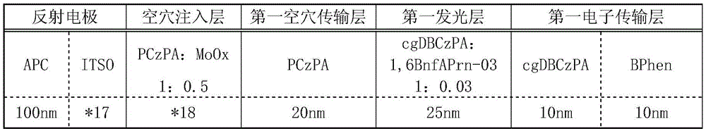
后面接*20→ followed by *20→
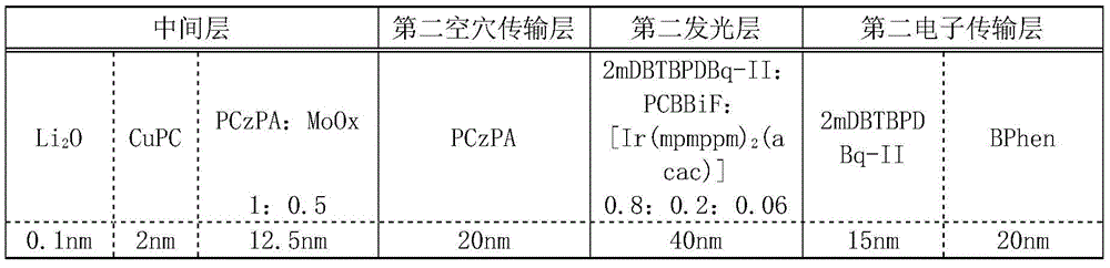
*20 后面接*21→*20 followed by *21→

*21*twenty one
*17发光元件8:85nm,发光元件9:65nm*17 light emitting element 8: 85nm, light emitting element 9: 65nm
*18发光元件8:40nm,发光元件9:45nm*18 light emitting element 8: 40nm, light emitting element 9: 45nm
*19发光元件8:蓝色0.8μm,发光元件9:黄色0.8μm*19 Light emitting element 8: Blue 0.8 μm, Light emitting element 9: Yellow 0.8 μm
在氮气氛的手套箱中,以不使发光元件暴露于大气的方式使用玻璃衬底对发光元件8(蓝色)及发光元件9(黄色)进行密封(将密封剂涂敷在元件的周围,在密封时进行UV处理(波长为365nm,6J/cm2)以及80℃的温度下的1小时的热处理),然后测定初期特性。该测定在室温下(在保持为25℃的气氛中)进行。在发光元件8中对穿过蓝色滤色片的光进行测定,在发光元件9中对穿过黄色滤色片的光进行测定。In a nitrogen atmosphere glove box, the light-emitting element 8 (blue) and the light-emitting element 9 (yellow) were sealed with a glass substrate in such a manner that the light-emitting element was not exposed to the atmosphere (the sealant was applied around the element, UV treatment (wavelength: 365 nm, 6 J/cm 2 ) and heat treatment at a temperature of 80° C. for 1 hour) were performed at the time of sealing, and then the initial characteristics were measured. This measurement is performed at room temperature (in an atmosphere kept at 25°C). The light passing through the blue color filter is measured in the
图39示出发光元件8(蓝色)及发光元件9(黄色)的亮度-电流密度特性,图40示出电流效率-亮度特性,图41示出亮度-电压特性,图42示出电流-电压特性,图43示出发射光谱。如附图所示,发光元件8及发光元件9示出良好的特性。39 shows the luminance-current density characteristics of light-emitting element 8 (blue) and light-emitting element 9 (yellow), FIG. 40 shows current efficiency-luminance characteristics, FIG. 41 shows luminance-voltage characteristics, and FIG. 42 shows current-voltage characteristics. Voltage characteristics, Figure 43 shows the emission spectrum. As shown in the drawings, the light-emitting
接着,对发光元件8(蓝色)及发光元件9(黄色)进行驱动试验,其中,在电流密度为恒定且初始亮度分别为300cd/m2和3000cd/m2。图44示出初始亮度为100%时的相对于驱动时间的亮度变化。Next, a driving test was performed on the light-emitting element 8 (blue) and the light-emitting element 9 (yellow), where the current density was constant and the initial luminance was 300 cd/m 2 and 3000 cd/m 2 , respectively. FIG. 44 shows changes in luminance with respect to driving time when the initial luminance is 100%.
从图44可知,发光元件8的亮度降低至初始亮度的90%而需要的时间大约为2300小时,发光元件9所需要的时间大约为6000小时。由此可知,本发明的一个方式的发光装置的功耗非常低,但是亮度劣化小,实用可靠性高。It can be seen from FIG. 44 that the time required for the luminance of the light-emitting
实施例4Example 4
在本实施例中,在实际上利用白色滤色片方式制造254ppi的发光装置。图37示出所制造的发光装置的照片。在每个像素中,50μm×50μm的红色、黄色、绿色及蓝色的子像素被配置为“田”字状。图38示出该发光装置与使用红色、绿色、蓝色的子像素的白色滤色片方式的比较例子的发光装置的显示静态图像时的功耗对比。算出峰值亮度为300cd/m2且显示各种静态图像时的面板部的功耗。In this embodiment, a 254ppi light emitting device is actually produced by using a white color filter method. Fig. 37 shows a photograph of the fabricated light emitting device. In each pixel, red, yellow, green and blue sub-pixels of 50 μm×50 μm are arranged in a “field” shape. FIG. 38 shows a comparison of power consumption when displaying a still image between this light-emitting device and a light-emitting device of a comparative example of a white filter system using red, green, and blue sub-pixels. Calculate the power consumption of the panel section when the peak luminance is 300cd/m 2 and various still images are displayed.
从图38可以明显知道实施例的发光装置的功耗比比较例子的发光装置低。尤其是,在白色显示部多的图像中,本发明的低功耗化的效果很明显。单位面积的面板功耗在白色显示的区域大的静态图像中最高,随着黒色显示的区域增加而降低。这是因为在黒色显示的区域中,液晶需要一直使背光发光,而OLED可以处于非发光状态。It is apparent from FIG. 38 that the light emitting device of the embodiment has lower power consumption than the light emitting device of the comparative example. In particular, in an image with many white display portions, the effect of the reduction in power consumption of the present invention is remarkable. Panel power consumption per unit area is highest in still images with large areas displayed in white, and decreases as the area displayed in black increases. This is because in the black display area, the liquid crystal needs to keep the backlight emitting light, while the OLED can be in a non-emitting state.
(参考例子)(reference example)
在本参考例子中,对在实施例中使用的有机化合物,即N,N’-(芘-1,6-二基)双[(6,N-二苯基苯并[b]萘并[1,2-d]呋喃)-8-胺](简称:1,6BnfAPrn-03)的合成方法进行说明。以下示出1,6BnfAPrn-03的结构。In this reference example, for the organic compound used in the examples, that is, N,N'-(pyrene-1,6-diyl)bis[(6,N-diphenylbenzo[b]naphtho[ 1,2-d]furan)-8-amine] (abbreviation: 1,6BnfAPrn-03) synthesis method will be described. The structure of 1,6BnfAPrn-03 is shown below.
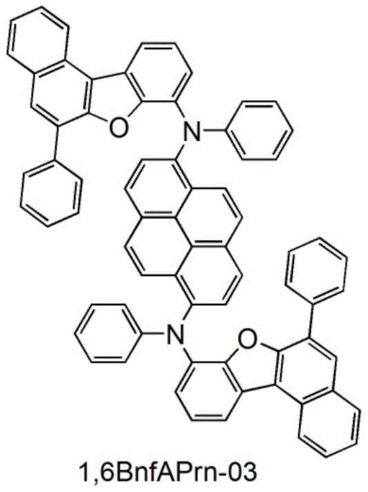
<步骤1:6-碘苯并[b]萘并[1,2-d]呋喃的合成><Step 1: Synthesis of 6-iodobenzo[b]naphtho[1,2-d]furan>
将8.5g(39mmol)的苯并[b]萘并[1,2-d]呋喃放在500mL三口烧瓶中,对烧瓶内进行氮气置换,然后添加195mL的四氢呋喃(THF)。将该溶液冷却到-75℃,然后将25mL(40mmol)的正丁基锂(1.59mol/L正己烷溶液)滴加到该溶液中。在滴加之后,在室温下搅拌该溶液1小时。8.5 g (39 mmol) of benzo[b]naphtho[1,2-d]furan was placed in a 500 mL three-neck flask, nitrogen was replaced in the flask, and then 195 mL of tetrahydrofuran (THF) was added. The solution was cooled to -75°C, and then 25 mL (40 mmol) of n-butyllithium (1.59 mol/L n-hexane solution) was added dropwise to the solution. After the dropwise addition, the solution was stirred at room temperature for 1 hour.
在经过规定时间之后,将该溶液冷却到-75℃,对该溶液滴加将10g(40mmol)的碘溶解于40mL的THF的溶液。在滴加之后,在将所得到的溶液回升至室温的同时搅拌17小时。在经过规定时间之后,对该混合物加入硫代硫酸钠水溶液搅拌1小时,然后使用水洗涤该混合物的有机层,使用硫酸镁使有机层干燥。在干燥之后,对该混合物进行重力过滤,通过使所得到的溶液通过硅藻土(Celite,日本和光纯药工业公司,目录号码:531-16855)、硅酸镁(Florisil,日本和光纯药工业公司,目录号码:540-00135)进行抽滤。浓缩所得到的滤液来得到固体,使用甲苯对其进行再结晶,以45%的收率得到6.0g(18mmol)的目的物的白色粉末。以下示出步骤1的合成方案。After a predetermined time elapsed, the solution was cooled to -75°C, and a solution of 10 g (40 mmol) of iodine dissolved in 40 mL of THF was added dropwise to the solution. After the dropwise addition, the resulting solution was stirred for 17 hours while returning to room temperature. After a predetermined time elapsed, an aqueous sodium thiosulfate solution was added to the mixture and stirred for 1 hour, and then the organic layer of the mixture was washed with water, and the organic layer was dried with magnesium sulfate. After drying, the mixture was subjected to gravity filtration by passing the resulting solution through diatomaceous earth (Celite, Wako Pure Chemical Industries, Japan, catalog number: 531-16855), magnesium silicate (Florisil, Wako Pure Chemical Industries, Japan Company, catalog number: 540-00135) for suction filtration. The obtained filtrate was concentrated to obtain a solid, which was recrystallized using toluene to obtain 6.0 g (18 mmol) of a white powder of the target object at a yield of 45%. The synthesis scheme of

<步骤2:6-苯基苯并[b]萘并[1,2-d]呋喃的合成><Step 2: Synthesis of 6-phenylbenzo[b]naphtho[1,2-d]furan>
将6.0g(18mmol)的6-碘苯并[b]萘并[1,2-d]呋喃、2.4g(19mmol)的苯硼酸、70mL的甲苯、20mL的乙醇及22mL的碳酸钾水溶液(2.0mol/L)放在200mL三口烧瓶中。在对该混合物进行减压的同时,搅拌该混合物而脱气。在脱气之后,对烧瓶内进行氮气置换,加入480mg(0.42mmol)的四(三苯基膦)钯(0)。在氮气流下以90℃搅拌该混合物12小时。6.0g (18mmol) of 6-iodobenzo[b]naphtho[1,2-d]furan, 2.4g (19mmol) of phenylboronic acid, 70mL of toluene, 20mL of ethanol and 22mL of potassium carbonate aqueous solution (2.0 mol/L) was placed in a 200mL three-necked flask. While depressurizing the mixture, the mixture was stirred to degas. After degassing, the inside of the flask was replaced with nitrogen, and 480 mg (0.42 mmol) of tetrakis(triphenylphosphine)palladium(0) was added. The mixture was stirred at 90°C for 12 hours under nitrogen flow.
在经过规定时间之后,将水加入到该混合物中,并用甲苯对水层进行萃取。混合所得到的萃取溶液和有机层,使用水进行洗涤,然后使用硫酸镁干燥。对该混合物进行重力过滤,浓缩所得到的滤液来得到固体,将其溶解于甲苯。通过使所得到的溶液通过硅藻土(日本和光纯药工业公司,目录号码:531-16855)、硅酸镁(日本和光纯药工业公司,目录号码:540-00135)、矾土进行抽滤。浓缩所得到的滤液来得到固体,使用甲苯对其进行再结晶,以93%的收率得到4.9g(17mmol)的目的物的白色固体。以下示出步骤2的合成方案。After the lapse of a prescribed time, water was added to the mixture, and the aqueous layer was extracted with toluene. The obtained extract solution and the organic layer were mixed, washed with water, and dried over magnesium sulfate. The mixture was gravity filtered and the resulting filtrate was concentrated to give a solid which was dissolved in toluene. Suction filtration was performed by passing the resulting solution through diatomaceous earth (Wako Pure Chemical Industries, catalog number: 531-16855), magnesium silicate (Wako Pure Chemical Industries, Japan, catalog number: 540-00135), alumina . The obtained filtrate was concentrated to obtain a solid, which was recrystallized using toluene to obtain 4.9 g (17 mmol) of a white solid of the target object at a yield of 93%. The synthesis scheme of
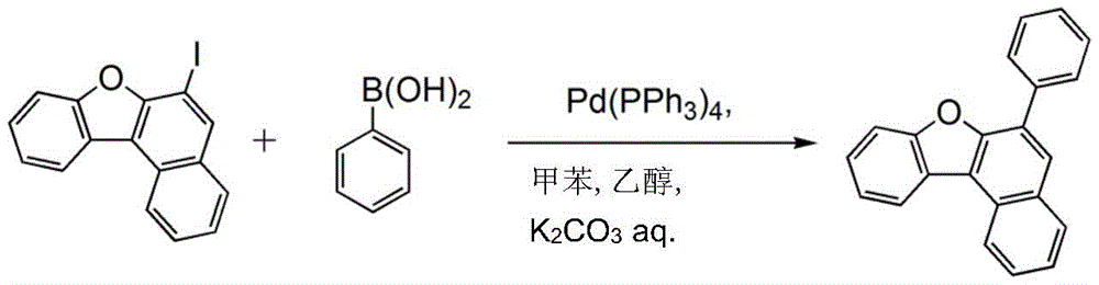
<步骤3:8-碘-6-苯基苯并[b]萘并[1,2,d]呋喃的合成><Step 3: Synthesis of 8-iodo-6-phenylbenzo[b]naphtho[1,2,d]furan>
将4.9g(17mmol)的6-苯基苯并[b]萘并[1,2-d]呋喃放在300mL三口烧瓶中,对烧瓶内进行氮气置换,然后添加87mL的四氢呋喃(THF)。将该溶液冷却到-75℃,然后将11mL(18mmol)的正丁基锂(1.59mol/L正己烷溶液)滴加到该溶液中。在滴加之后,在室温下搅拌该溶液1小时。在经过规定时间之后,将该溶液冷却到-75℃,对该溶液滴加将4.6g(18mmol)的碘溶解于18mL的THF的溶液。Put 4.9g (17mmol) of 6-phenylbenzo[b]naphtho[1,2-d]furan in a 300mL three-necked flask, replace the flask with nitrogen, and then add 87mL of tetrahydrofuran (THF). The solution was cooled to -75°C, and then 11 mL (18 mmol) of n-butyllithium (1.59 mol/L n-hexane solution) was added dropwise to the solution. After the dropwise addition, the solution was stirred at room temperature for 1 hour. After a predetermined time had elapsed, the solution was cooled to -75°C, and a solution of 4.6 g (18 mmol) of iodine dissolved in 18 mL of THF was added dropwise to the solution.
在将所得到的溶液回升至室温的同时搅拌17小时。在经过规定时间之后,对该混合物加入硫代硫酸钠水溶液搅拌1小时,然后使用水洗涤该混合物的有机层,使用硫酸镁使有机层干燥。对该混合物进行重力过滤,通过使所得到的溶液通过硅藻土(日本和光纯药工业公司,目录号码:531-16855)、硅酸镁(日本和光纯药工业公司,目录号码:540-00135)及矾土进行抽滤。浓缩所得到的滤液来得到固体,使用甲苯对其进行再结晶,以53%的收率得到3.7g(8.8mmol)的目的物的白色固体。以下示出步骤3的合成方案。The resulting solution was stirred for 17 hours while returning to room temperature. After a predetermined time elapsed, an aqueous sodium thiosulfate solution was added to the mixture and stirred for 1 hour, and then the organic layer of the mixture was washed with water, and the organic layer was dried with magnesium sulfate. The mixture was subjected to gravity filtration by passing the resulting solution through diatomaceous earth (Wako Pure Chemical Industries, catalog number: 531-16855), magnesium silicate (Wako Pure Chemical Industries, catalog number: 540-00135 ) and alumina for suction filtration. The obtained filtrate was concentrated to obtain a solid, which was recrystallized using toluene to obtain 3.7 g (8.8 mmol) of a white solid of the target object at a yield of 53%. The synthesis scheme of Step 3 is shown below.
<步骤4:1,6BnfAPrn-03的合成><Step 4: Synthesis of 1,6BnfAPrn-03>
将0.71g(2.0mmol)的1,6-二溴芘、1.0g(10.4mmol)的叔丁醇钠、10mL的甲苯、0.36mL(4.0mmol)的苯胺及0.3mL的三(叔丁基)膦(10wt%己烷溶液)放在100mL三口烧瓶中,对烧瓶内进行氮气置换。对该混合物加入50mg(85μmol)的双(二亚苄基丙酮)钯(0),以80℃搅拌2小时。0.71g (2.0mmol) of 1,6-dibromopyrene, 1.0g (10.4mmol) of sodium tert-butoxide, 10mL of toluene, 0.36mL (4.0mmol) of aniline and 0.3mL of tri(tert-butyl) Phosphine (10 wt% hexane solution) was placed in a 100 mL three-necked flask, and the inside of the flask was replaced with nitrogen. 50 mg (85 μmol) of bis(dibenzylideneacetone)palladium(0) was added to the mixture, followed by stirring at 80° C. for 2 hours.
在经过规定时间之后,对所得到的混合物加入1.7g(4.0mmol)的8-碘-6-苯基苯并[b]萘并[1,2-d]呋喃、180mg(0.44mmol)的2-二环己基膦基-2’,6’-二甲氧基联苯(简称:S-Phos)及50mg(85μmol)的双(二亚苄基丙酮)钯(0),在100℃下搅拌该混合物15小时。在经过规定时间之后,将所得到的混合物通过硅藻土(日本和光纯药工业公司,目录号码:531-16855)进行过滤。使用乙醇对通过浓缩所得到的滤液来得到的固体进行洗涤并使用甲苯进行再结晶,以71%的收率得到1.38g(1.4mmol)的目的物的黄色固体。After the specified time, 1.7 g (4.0 mmol) of 8-iodo-6-phenylbenzo[b]naphtho[1,2-d]furan, 180 mg (0.44 mmol) of 2 -Dicyclohexylphosphino-2',6'-dimethoxybiphenyl (abbreviation: S-Phos) and 50 mg (85 μmol) of bis(dibenzylideneacetone) palladium (0), stirred at 100 ° C The mixture was 15 hours. After a prescribed time elapsed, the resulting mixture was filtered through celite (Wako Pure Chemical Industries, Ltd., catalog number: 531-16855). The solid obtained by concentrating the obtained filtrate was washed with ethanol and recrystallized with toluene to obtain 1.38 g (1.4 mmol) of a yellow solid of the target object at a yield of 71%.
通过利用梯度升华(train sublimation)方法对所得到的黄色固体1.37mg(1.4mmol)进行升华精炼。在升华精炼中,在氩流量为10mL/min、压力为2.3Pa的条件下以370℃加热黄色固体。在进行升华精炼之后,以50%的收率得到0.68g(0.70mmol)的黄色固体。以下示出步骤4的合成方案。1.37 mg (1.4 mmol) of the obtained yellow solid was subjected to sublimation refinement by a gradient sublimation method. In sublimation refining, the yellow solid was heated at 370° C. under the conditions of an argon flow rate of 10 mL/min and a pressure of 2.3 Pa. After refining by sublimation, 0.68 g (0.70 mmol) of a yellow solid was obtained in a yield of 50%. The synthesis scheme of

以下示出利用核磁共振法(1H-NMR)来分析通过上述步骤4得到的黄色固体的结果。由其结果可知:得到了1,6BnfAPrn-03。The results of analyzing the yellow solid obtained in
1H NMR(二氯甲烷-d2、500MHz):δ=6.88(t,J=7.7Hz,4H),7.03-7.06(m,6H),7.11(t,J=7.5Hz,2H),7.13(d,J=8.0Hz,2H),7.28-7.32(m,8H),7.37(t,J=8.0Hz,2H),7.59(t,J=7.2Hz,2H),7.75(t,J=7.7Hz,2H),7.84(d,J=9.0Hz,2H),7.88(d,J=8.0Hz,2H),8.01(s,2H),8.07(d,J=8.0Hz,4H),8.14(d,J=9.0Hz,2H),8.21(d,J=8.0Hz,2H),8.69(d,J=8.5Hz,2H)。 1 H NMR (dichloromethane-d2, 500MHz): δ=6.88(t, J=7.7Hz, 4H), 7.03-7.06(m, 6H), 7.11(t, J=7.5Hz, 2H), 7.13( d, J=8.0Hz, 2H), 7.28-7.32(m, 8H), 7.37(t, J=8.0Hz, 2H), 7.59(t, J=7.2Hz, 2H), 7.75(t, J=7.7 Hz, 2H), 7.84(d, J=9.0Hz, 2H), 7.88(d, J=8.0Hz, 2H), 8.01(s, 2H), 8.07(d, J=8.0Hz, 4H), 8.14( d, J=9.0 Hz, 2H), 8.21 (d, J=8.0 Hz, 2H), 8.69 (d, J=8.5 Hz, 2H).
符号说明Symbol Description
101:第一电极;102:第二电极;103a:EL层;103b:EL层;104a:空穴注入层;104b:空穴注入层;105a:空穴传输层;105b:空穴传输层;106:发光层;106a:发光层;106b:发光层;107a:电子传输层;107b:电子传输层;108a:电子注入层;108b:电子注入层;109:电荷产生层;113:第一发光层;114:第二发光层;121:客体材料(荧光材料);122:主体材料;131:客体材料(磷光材料);132:第一有机化合物;133:第二有机化合物;134:激基复合物;501:衬底;502:FET;503:第一电极;504:分隔壁;505:EL层;506R:发光区域;506G:发光区域;506B:发光区域;506W:发光区域;506Y:发光区域;507R:发光元件;507G:发光元件;507B:发光元件;507W:发光元件;507Y:发光元件;508R:着色层;508G:着色层;508B:着色层;508Y:着色层;509:黑色层(黑矩阵);510:第二电极;511:密封衬底;601:元件衬底;602:像素部;603:驱动电路部(源极线驱动电路);604a:驱动电路部(栅极线驱动电路);604b:驱动电路部(栅极线驱动电路);605:密封材料;606:密封衬底;607:布线;608:FPC(柔性印刷电路);609:FET;610:FET;611:开关FET;612:电流控制FET;613:第一电极(阳极);614:绝缘物;615:EL层;616:第二电极(阴极);617:发光元件;618:空间;1100:衬底;1102B:第一电极;1102G:第一电极;1102Y:第一电极;1102R:第一电极;1103d:蓝色发光层;1103e:空穴注入层及空穴传输层;1103f:黄色发光层;1103h:电子传输层及电子注入层;1104:第二电极;1105:黑矩阵;1106B:滤色片;1106G:滤色片;1106Y:滤色片;1106R:滤色片;1101:密封衬底;2000:触控面板;2001:触控面板;2501:显示部;2502R:像素;2502t:晶体管;2503c:电容器;2503g:扫描线驱动电路;2503t:晶体管;2509:FPC;2510:衬底;2511:布线;2519:端子;2521:绝缘层;2528:分隔壁;2550R:发光元件;2560:密封层;2567BM:遮光层;2567p:反射防止层;2567R:着色层;2570:衬底;2580R:发光模块;2590:衬底;2591:电极;2592:电极;2593:绝缘层;2594:布线;2595:触摸传感器;2597:粘合层;2598:布线;2599:连接层;2601:脉冲电压输出电路;2602:电流检测电路;2603:电容器;2611:晶体管;2612:晶体管;2613:晶体管;2621:电极;2622:电极;7100:电视装置;7101:外壳;7103:显示部;7105:支架;7107:显示部;7109:操作键;7110:遥控操作机;7201:主体;7202:外壳;7203:显示部;7204:键盘;7205:外部连接端口;7206:指向装置;7302:外壳;7304:显示面板;7305:表示时间的图标;7306:其他图标;7311:操作按钮;7312:操作按钮;7313:连接端子;7321:腕带;7322:表带扣;7400:移动电话机;7401:外壳;7402:显示部;7403:操作按钮;7404:外部连接部;7405:扬声器;7406:麦克风;7407:照相机;7500(1):外壳;7500(2):外壳;7501(1):显示部;7501(2):显示部;7502(1):显示部;7502(2):显示部;8001:照明装置;8002:照明装置;8003:照明装置;8004:照明装置;9310:便携式信息终端;9311:显示面板;9312:显示区域;9313:铰链;9315:外壳101: first electrode; 102: second electrode; 103a: EL layer; 103b: EL layer; 104a: hole injection layer; 104b: hole injection layer; 105a: hole transport layer; 105b: hole transport layer; 106: light emitting layer; 106a: light emitting layer; 106b: light emitting layer; 107a: electron transport layer; 107b: electron transport layer; 108a: electron injection layer; 108b: electron injection layer; 109: charge generation layer; 113: first light emitting layer layer; 114: second light-emitting layer; 121: guest material (fluorescent material); 122: host material; 131: guest material (phosphorescent material); 132: first organic compound; 133: second organic compound; 134: excimer Compound; 501: substrate; 502: FET; 503: first electrode; 504: partition wall; 505: EL layer; 506R: light emitting region; 506G: light emitting region; 506B: light emitting region; 506W: light emitting region; 507R: light emitting element; 507G: light emitting element; 507B: light emitting element; 507W: light emitting element; 507Y: light emitting element; 508R: colored layer; 508G: colored layer; 508B: colored layer; 508Y: colored layer; Black layer (black matrix); 510: second electrode; 511: sealing substrate; 601: element substrate; 602: pixel part; 603: driving circuit part (source line driving circuit); 604a: driving circuit part (gate electrode line driving circuit); 604b: driving circuit part (gate line driving circuit); 605: sealing material; 606: sealing substrate; 607: wiring; 608: FPC (flexible printed circuit); 609: FET; 610: FET 611: switch FET; 612: current control FET; 613: first electrode (anode); 614: insulator; 615: EL layer; 616: second electrode (cathode); 617: light emitting element; 618: space; 1100 : substrate; 1102B: first electrode; 1102G: first electrode; 1102Y: first electrode; 1102R: first electrode; 1103d: blue light emitting layer; 1103e: hole injection layer and hole transport layer; 1103f: yellow Light emitting layer; 1103h: electron transport layer and electron injection layer; 1104: second electrode; 1105: black matrix; 1106B: color filter; 1106G: color filter; 1106Y: color filter; 1106R: color filter; 1101: Sealing substrate; 2000: touch panel; 2001: touch panel; 2501: display unit; 2502R: pixel; 2502t: transistor; 2503c: capacitor; 2503g: scanning line drive circuit; 2503t: transistor; 2509: FPC; Substrate; 2511: Wiring; 2519: Terminal; 2521: Insulating layer; 2528: Partition wall; 2550R: Light emitting element; 25 60: sealing layer; 2567BM: light shielding layer; 2567p: anti-reflection layer; 2567R: colored layer; 2570: substrate; 2580R: light emitting module; 2590: substrate; 2591: electrode; 2592: electrode; 2593: insulating layer; 2594 : Wiring; 2595: Touch sensor; 2597: Adhesive layer; 2598: Wiring; 2599: Connection layer; 2601: Pulse voltage output circuit; 2602: Current detection circuit; 2603: Capacitor; 2611: Transistor; 2612: Transistor; 2613: Transistor; 2621: electrode; 2622: electrode; 7100: television device; 7101: casing; 7103: display part; 7105: bracket; 7107: display part; 7109: operation key; Housing; 7203: display unit; 7204: keyboard; 7205: external connection port; 7206: pointing device; 7302: housing; 7304: display panel; 7305: icon indicating time; 7306: other icons; Operation button; 7313: connection terminal; 7321: wristband; 7322: strap buckle; 7400: mobile phone; 7401: casing; 7402: display part; 7403: operation button; 7404: external connection part; 7405: speaker; 7406 : Microphone; 7407: Camera; 7500(1): Housing; 7500(2): Housing; 7501(1): Display; 7501(2): Display; 7502(1): Display; 7502(2): Display part; 8001: lighting device; 8002: lighting device; 8003: lighting device; 8004: lighting device; 9310: portable information terminal; 9311: display panel; 9312: display area; 9313: hinge; 9315: shell
本申请基于2014年8月8日提交到日本专利局的日本专利申请No.2014-162532、2014年8月8日提交到日本专利局的日本专利申请No.2014-162576、2014年11月28日提交到日本专利局的日本专利申请No.2014-241188以及2015年6月30日提交到日本专利局的日本专利申请No.2015-131156,通过引用将其完整内容并入在此。This application is based on Japanese Patent Application No.2014-162532 submitted to the Japan Patent Office on August 8, 2014, Japanese Patent Application No.2014-162576 submitted to the Japan Patent Office on August 8, 2014, and Japanese Patent Application No. 2014-162576 filed on November 28, 2014 Japanese Patent Application No. 2014-241188 filed with the Japan Patent Office on June 30, 2015 and Japanese Patent Application No. 2015-131156 filed with the Japan Patent Office on June 30, 2015, the entire contents of which are hereby incorporated by reference.
Claims (15)
Applications Claiming Priority (10)
| Application Number | Priority Date | Filing Date | Title |
|---|---|---|---|
| JP2014-162576 | 2014-08-08 | ||
| JP2014162532 | 2014-08-08 | ||
| JP2014-162532 | 2014-08-08 | ||
| JP2014162576 | 2014-08-08 | ||
| JP2014-241188 | 2014-11-28 | ||
| JP2014241188 | 2014-11-28 | ||
| JP2015-131156 | 2015-06-30 | ||
| JP2015131156 | 2015-06-30 | ||
| CN201580042349.4A CN106575713B (en) | 2014-08-08 | 2015-07-30 | Light-emitting device, electronic equipment, and lighting device |
| PCT/IB2015/055749 WO2016020801A1 (en) | 2014-08-08 | 2015-07-30 | Light-emitting device, electronic device, and lighting device |
Related Parent Applications (1)
| Application Number | Title | Priority Date | Filing Date |
|---|---|---|---|
| CN201580042349.4A Division CN106575713B (en) | 2014-08-08 | 2015-07-30 | Light-emitting device, electronic equipment, and lighting device |
Publications (2)
| Publication Number | Publication Date |
|---|---|
| CN109742262A CN109742262A (en) | 2019-05-10 |
| CN109742262B true CN109742262B (en) | 2022-11-22 |
Family
ID=55263231
Family Applications (2)
| Application Number | Title | Priority Date | Filing Date |
|---|---|---|---|
| CN201910024880.9A Active CN109742262B (en) | 2014-08-08 | 2015-07-30 | Light-emitting device, electronic apparatus, and lighting device |
| CN201580042349.4A Active CN106575713B (en) | 2014-08-08 | 2015-07-30 | Light-emitting device, electronic equipment, and lighting device |
Family Applications After (1)
| Application Number | Title | Priority Date | Filing Date |
|---|---|---|---|
| CN201580042349.4A Active CN106575713B (en) | 2014-08-08 | 2015-07-30 | Light-emitting device, electronic equipment, and lighting device |
Country Status (7)
| Country | Link |
|---|---|
| US (3) | US9876056B2 (en) |
| JP (3) | JP6684058B2 (en) |
| KR (2) | KR102879924B1 (en) |
| CN (2) | CN109742262B (en) |
| DE (2) | DE112015007286B4 (en) |
| TW (2) | TWI681579B (en) |
| WO (1) | WO2016020801A1 (en) |
Families Citing this family (33)
| Publication number | Priority date | Publication date | Assignee | Title |
|---|---|---|---|---|
| CN109742262B (en) * | 2014-08-08 | 2022-11-22 | 株式会社半导体能源研究所 | Light-emitting device, electronic apparatus, and lighting device |
| US9991471B2 (en) * | 2014-12-26 | 2018-06-05 | Semiconductor Energy Laboratory Co., Ltd. | Light-emitting element, light-emitting device, display device, and electronic device |
| TWI860824B (en) * | 2015-03-09 | 2024-11-01 | 日商半導體能源研究所股份有限公司 | Light-emitting element, display device, electronic device, and lighting device |
| TWI737594B (en) * | 2015-03-09 | 2021-09-01 | 日商半導體能源研究所股份有限公司 | Light-emitting element, display device, electronic device, and lighting device |
| KR102398677B1 (en) * | 2015-04-06 | 2022-05-16 | 삼성디스플레이 주식회사 | Display device |
| US10439146B2 (en) * | 2015-08-07 | 2019-10-08 | Semiconductor Energy Laboratory Co., Ltd. | Organic compound, light-emitting element, light-emitting device, electronic device, and lighting device |
| WO2017130079A1 (en) | 2016-01-29 | 2017-08-03 | Semiconductor Energy Laboratory Co., Ltd. | Light-emitting element, light-emitting device, electronic device, and lighting device |
| CN105511118B (en) * | 2016-02-03 | 2018-09-11 | 京东方科技集团股份有限公司 | A kind of display device |
| CN108886856B (en) * | 2016-03-29 | 2020-04-10 | 夏普株式会社 | Organic EL display device and method for manufacturing organic EL display device |
| KR102353663B1 (en) | 2016-05-20 | 2022-01-19 | 가부시키가이샤 한도오따이 에네루기 켄큐쇼 | Light-emitting element, light-emitting device, electronic device, and lighting device |
| KR20180002505A (en) | 2016-06-29 | 2018-01-08 | 가부시키가이샤 한도오따이 에네루기 켄큐쇼 | Manufacturing method of light-emitting element |
| TWI856504B (en) | 2016-09-14 | 2024-09-21 | 日商半導體能源研究所股份有限公司 | Organic compound, light-emitting element, light-emitting device, electronic device, and lighting device |
| US10741769B2 (en) | 2016-10-14 | 2020-08-11 | Semiconductor Energy Laboratory Co., Ltd. | Organic compound, light-emitting element, light-emitting device, electronic device, and lighting device |
| CN108122941A (en) * | 2016-11-28 | 2018-06-05 | 南昌欧菲生物识别技术有限公司 | Organic light-emitting diode (OLED) display screen fingerprint identification device and electronic equipment |
| KR102701648B1 (en) | 2016-12-28 | 2024-09-03 | 가부시키가이샤 한도오따이 에네루기 켄큐쇼 | Organic compound, light-emitting element, light-emitting device, electronic device, display device, and lighting device |
| KR102878528B1 (en) * | 2017-02-28 | 2025-10-29 | 엘지디스플레이 주식회사 | Electroluminescent Display Device |
| US10529780B2 (en) * | 2017-02-28 | 2020-01-07 | Semiconductor Energy Laboratory Co., Ltd. | Display device, display module, and electronic device |
| TWI782973B (en) * | 2017-04-07 | 2022-11-11 | 日商半導體能源硏究所股份有限公司 | Light-emitting element, display device, electronic device, and lighting device |
| DE102017109254A1 (en) * | 2017-04-28 | 2018-10-31 | Carl Zeiss Ag | digital camera |
| CN107275501A (en) * | 2017-06-13 | 2017-10-20 | 上海天马有机发光显示技术有限公司 | Organic light-emitting structure, display device and mobile terminal |
| US10892432B2 (en) | 2017-09-26 | 2021-01-12 | Sharp Kabushiki Kaisha | Organic EL display device, manufacturing method thereof, and light-emission method thereof |
| CN108417179B (en) * | 2018-05-16 | 2023-12-05 | 京东方科技集团股份有限公司 | Light emitting devices and display devices |
| US12089490B2 (en) | 2018-07-31 | 2024-09-10 | Semiconductor Energy Laboratory Co., Ltd. | Organic compound, light-emitting element, light-emitting device, electronic device, and lighting device |
| US11450694B2 (en) | 2018-08-21 | 2022-09-20 | Semiconductor Energy Laboratory Co., Ltd. | Display apparatus and electronic device |
| CN111261665A (en) * | 2018-12-03 | 2020-06-09 | 昆山工研院新型平板显示技术中心有限公司 | Quantum dot light-emitting device, preparation method thereof and display device |
| CN111261666A (en) * | 2018-12-03 | 2020-06-09 | 昆山工研院新型平板显示技术中心有限公司 | Display panel and display device |
| KR102785782B1 (en) * | 2019-02-07 | 2025-03-24 | 삼성디스플레이 주식회사 | Organic light emitting display device including quantum dot color convert filter |
| CN110034166B (en) | 2019-03-26 | 2022-09-09 | 武汉华星光电半导体显示技术有限公司 | Organic light emitting diode display device and method of manufacturing the same |
| CN110112181A (en) * | 2019-04-09 | 2019-08-09 | 深圳市华星光电半导体显示技术有限公司 | Organic light emitting diodde desplay device and preparation method thereof |
| KR102760407B1 (en) * | 2019-09-04 | 2025-02-04 | 삼성디스플레이 주식회사 | Organic light emitting diode and display device having the same |
| US11968898B2 (en) * | 2019-10-24 | 2024-04-23 | Lg Display Co., Ltd. | Organic light emitting diode and organic light emitting device including the same |
| TWI750706B (en) | 2020-06-20 | 2021-12-21 | 丁逸聖 | Light-emitting device, light-emitting method, light detection device, spectrum detection method, and light-emitting correction method |
| JP7665428B2 (en) * | 2021-06-08 | 2025-04-21 | キヤノン株式会社 | Organic electroluminescence device |
Citations (2)
| Publication number | Priority date | Publication date | Assignee | Title |
|---|---|---|---|---|
| CN102456840A (en) * | 2010-10-21 | 2012-05-16 | 乐金显示有限公司 | Organic light emitting diode device |
| CN102751441A (en) * | 2011-04-21 | 2012-10-24 | 松下电器产业株式会社 | White organic electroluminescence device |
Family Cites Families (52)
| Publication number | Priority date | Publication date | Assignee | Title |
|---|---|---|---|---|
| JP2004200141A (en) | 2002-10-24 | 2004-07-15 | Toyota Industries Corp | Organic EL device |
| WO2005010012A1 (en) | 2003-07-28 | 2005-02-03 | Semiconductor Energy Laboratory Co., Ltd. | Luminescent organic compound and light-emitting device using same |
| US7232619B2 (en) | 2003-10-03 | 2007-06-19 | Semiconductor Energy Laboratory Co., Ltd. | Pyrene derivative, light emitting element, and light emitting device |
| TW200541401A (en) | 2004-02-13 | 2005-12-16 | Idemitsu Kosan Co | Organic electroluminescent device |
| KR100685407B1 (en) * | 2004-10-18 | 2007-02-22 | 삼성에스디아이 주식회사 | Full color organic light emitting display device with red, green, blue, cyan, magenta and yellow color control layers |
| US7838128B2 (en) | 2005-07-14 | 2010-11-23 | Semiconductor Energy Laboratory Co., Ltd. | Carbazole derivative, and light emitting element material, light emitting element, and electronic appliance obtained using the same |
| JP2007045816A (en) * | 2005-07-14 | 2007-02-22 | Semiconductor Energy Lab Co Ltd | Carbazole derivative, material for light emitting element, light emitting element and electronic device obtained by using the same |
| TWI362409B (en) * | 2007-09-06 | 2012-04-21 | Show An Chen | Electroluminescent conjugated polymers grafted with charge transporting moieties having graded ionization potential or electrophilic property and their application in light-emitting diodes |
| US8040047B2 (en) | 2007-10-19 | 2011-10-18 | Semiconductor Energy Laboratory Co., Ltd. | Light-emitting device |
| EP2110369A1 (en) | 2008-03-25 | 2009-10-21 | Semiconductor Energy Laboratory Co., Ltd. | Method of synthesizing 9-aryl-10-iodoanthracene derivative and light-emitting material |
| JP2009290051A (en) * | 2008-05-30 | 2009-12-10 | Toray Ind Inc | Light-emitting element |
| WO2009154575A1 (en) * | 2008-06-17 | 2009-12-23 | Armin Gerhard Aberle | Thin-film solar cell interconnection |
| JP5690482B2 (en) * | 2008-12-01 | 2015-03-25 | 株式会社半導体エネルギー研究所 | LIGHT EMITTING ELEMENT, LIGHT EMITTING DEVICE AND LIGHTING DEVICE |
| US8629430B2 (en) | 2009-05-29 | 2014-01-14 | Idemitsu Kosan Co., Ltd. | Anthracene derivative and organic electroluminescent element using the same |
| US8642190B2 (en) | 2009-10-22 | 2014-02-04 | Semiconductor Energy Laboratory Co., Ltd. | Fluorene derivative, light-emitting element, light-emitting device, electronic device, and lighting device |
| EP2366753B1 (en) * | 2010-03-02 | 2015-06-17 | Semiconductor Energy Laboratory Co., Ltd. | Light-Emitting Element and Lighting Device |
| US10570113B2 (en) | 2010-04-09 | 2020-02-25 | Semiconductor Energy Laboratory Co., Ltd. | Aromatic amine derivative, light-emitting element, light-emitting device, electronic device, and lighting device |
| KR102071726B1 (en) | 2010-10-22 | 2020-01-30 | 가부시키가이샤 한도오따이 에네루기 켄큐쇼 | Organometallic complex, light-emitting element, light-emitting device, electronic device and lighting device |
| US20120126205A1 (en) | 2010-11-22 | 2012-05-24 | Idemitsu Kosan Co., Ltd. | Organic electroluminescence device |
| US8883323B2 (en) | 2010-11-22 | 2014-11-11 | Idemitsu Kosan Co., Ltd. | Organic electroluminescence device |
| CN102668160B (en) | 2010-11-22 | 2016-06-22 | 出光兴产株式会社 | Organic Electroluminescent Devices |
| US9324950B2 (en) | 2010-11-22 | 2016-04-26 | Idemitsu Kosan Co., Ltd. | Organic electroluminescence device |
| WO2012086662A1 (en) * | 2010-12-24 | 2012-06-28 | Semiconductor Energy Laboratory Co., Ltd. | Lighting device |
| TWI518078B (en) * | 2010-12-28 | 2016-01-21 | 半導體能源研究所股份有限公司 | Benzo[b]naphtho[1,2-d]furan compound serving as a light-emitting element material |
| KR101894898B1 (en) | 2011-02-11 | 2018-09-04 | 가부시키가이샤 한도오따이 에네루기 켄큐쇼 | Light-emitting device and electronic device using light-emitting device |
| KR101914577B1 (en) * | 2011-02-11 | 2018-11-02 | 가부시키가이샤 한도오따이 에네루기 켄큐쇼 | Light-emitting element, light-emitting device, and display device |
| TW202542110A (en) * | 2011-02-28 | 2025-11-01 | 日商半導體能源研究所股份有限公司 | Light-emitting element |
| JP5182901B2 (en) * | 2011-03-24 | 2013-04-17 | パナソニック株式会社 | Organic electroluminescence device |
| TWI562424B (en) | 2011-03-25 | 2016-12-11 | Semiconductor Energy Lab Co Ltd | Light-emitting panel, light-emitting device, and method for manufacturing the light-emitting panel |
| KR101960759B1 (en) | 2011-04-08 | 2019-03-21 | 가부시키가이샤 한도오따이 에네루기 켄큐쇼 | Light-emitting device, electronic appliance, and lighting device |
| US9083000B2 (en) * | 2011-04-29 | 2015-07-14 | Semiconductor Energy Laboratory Co., Ltd. | Light-emitting element, light-emitting device, and lighting device |
| KR102126087B1 (en) * | 2011-10-11 | 2020-06-23 | 가부시키가이샤 한도오따이 에네루기 켄큐쇼 | Light-emitting element, light-emitting device, electronic device, lighting device, and pyrene-based compound |
| KR102250019B1 (en) * | 2012-03-14 | 2021-05-11 | 가부시키가이샤 한도오따이 에네루기 켄큐쇼 | Light-emitting element |
| DE112013001439B4 (en) | 2012-03-14 | 2022-01-20 | Semiconductor Energy Laboratory Co., Ltd. | Light-emitting device, electronic device and lighting device |
| JP2013232629A (en) | 2012-04-06 | 2013-11-14 | Semiconductor Energy Lab Co Ltd | Light-emitting element, light-emitting device, electronic device, and lighting device |
| JP6158542B2 (en) | 2012-04-13 | 2017-07-05 | 株式会社半導体エネルギー研究所 | LIGHT EMITTING ELEMENT, LIGHT EMITTING DEVICE, ELECTRONIC DEVICE, AND LIGHTING DEVICE |
| JP6158543B2 (en) | 2012-04-13 | 2017-07-05 | 株式会社半導体エネルギー研究所 | LIGHT EMITTING ELEMENT, LIGHT EMITTING DEVICE, ELECTRONIC DEVICE, AND LIGHTING DEVICE |
| JP6076153B2 (en) | 2012-04-20 | 2017-02-08 | 株式会社半導体エネルギー研究所 | LIGHT EMITTING ELEMENT, LIGHT EMITTING DEVICE, DISPLAY DEVICE, ELECTRONIC DEVICE, AND LIGHTING DEVICE |
| EP2687552A1 (en) | 2012-07-17 | 2014-01-22 | Huntsman International Llc | Use of polyurea nanoparticles as performance modifiers in polyurethane materials |
| KR102204794B1 (en) | 2012-08-10 | 2021-01-18 | 가부시키가이샤 한도오따이 에네루기 켄큐쇼 | Light-emitting element, light-emitting device, display device, electronic device, and lighting device |
| KR102081116B1 (en) * | 2012-09-06 | 2020-02-25 | 엘지디스플레이 주식회사 | Organic light emitting display device |
| KR20140071897A (en) | 2012-11-26 | 2014-06-12 | 가부시키가이샤 한도오따이 에네루기 켄큐쇼 | Light-emitting element, light-emitting device, electronic device, and lighting device |
| US9203045B2 (en) | 2012-11-29 | 2015-12-01 | Semiconductor Energy Laboratory Co., Ltd. | Light-emitting element, light-emitting device, electronic device, and lighting device |
| JP6155020B2 (en) | 2012-12-21 | 2017-06-28 | 株式会社半導体エネルギー研究所 | Light emitting device and manufacturing method thereof |
| JP6216125B2 (en) | 2013-02-12 | 2017-10-18 | 株式会社半導体エネルギー研究所 | Light emitting device |
| KR102763019B1 (en) * | 2013-05-16 | 2025-02-07 | 가부시키가이샤 한도오따이 에네루기 켄큐쇼 | Light-emitting element, light-emitting device, electronic device, and lighting device |
| KR102077143B1 (en) * | 2013-05-30 | 2020-02-14 | 삼성디스플레이 주식회사 | Organic light emitting display device and manufacturing method of the same |
| KR101969866B1 (en) | 2013-07-26 | 2019-04-17 | 가부시키가이샤 한도오따이 에네루기 켄큐쇼 | Organic compound, light-emitting element, light-emitting device, electronic appliance, and lighting device |
| TWI686971B (en) | 2013-08-09 | 2020-03-01 | 日商半導體能源研究所股份有限公司 | Light-emitting element, display module, lighting module, light-emitting device, display device, electronic device, and lighting device |
| TWI654775B (en) | 2013-10-16 | 2019-03-21 | 日商半導體能源研究所股份有限公司 | Light-emitting element, light-emitting device, electronic device and lighting device |
| JP2015187982A (en) * | 2014-03-13 | 2015-10-29 | 株式会社半導体エネルギー研究所 | Light-emitting element, light-emitting device, electronic apparatus, and lighting system |
| CN109742262B (en) * | 2014-08-08 | 2022-11-22 | 株式会社半导体能源研究所 | Light-emitting device, electronic apparatus, and lighting device |
-
2015
- 2015-07-30 CN CN201910024880.9A patent/CN109742262B/en active Active
- 2015-07-30 DE DE112015007286.1T patent/DE112015007286B4/en active Active
- 2015-07-30 WO PCT/IB2015/055749 patent/WO2016020801A1/en not_active Ceased
- 2015-07-30 KR KR1020227025005A patent/KR102879924B1/en active Active
- 2015-07-30 KR KR1020177005048A patent/KR102424714B1/en active Active
- 2015-07-30 CN CN201580042349.4A patent/CN106575713B/en active Active
- 2015-07-30 DE DE112015003690.3T patent/DE112015003690B4/en active Active
- 2015-08-05 JP JP2015154778A patent/JP6684058B2/en active Active
- 2015-08-05 US US14/818,951 patent/US9876056B2/en active Active
- 2015-08-06 TW TW104125701A patent/TWI681579B/en active
- 2015-08-06 TW TW108142210A patent/TWI700844B/en active
-
2018
- 2018-01-10 US US15/866,879 patent/US10854682B2/en active Active
-
2020
- 2020-03-27 JP JP2020057393A patent/JP6884902B2/en not_active Expired - Fee Related
- 2020-11-25 US US17/104,398 patent/US11917882B2/en active Active
-
2021
- 2021-05-12 JP JP2021080907A patent/JP2021176150A/en not_active Withdrawn
Patent Citations (2)
| Publication number | Priority date | Publication date | Assignee | Title |
|---|---|---|---|---|
| CN102456840A (en) * | 2010-10-21 | 2012-05-16 | 乐金显示有限公司 | Organic light emitting diode device |
| CN102751441A (en) * | 2011-04-21 | 2012-10-24 | 松下电器产业株式会社 | White organic electroluminescence device |
Also Published As
| Publication number | Publication date |
|---|---|
| US20160079314A1 (en) | 2016-03-17 |
| KR102424714B1 (en) | 2022-07-22 |
| KR20170042299A (en) | 2017-04-18 |
| JP2021176150A (en) | 2021-11-04 |
| KR20220107076A (en) | 2022-08-01 |
| TWI681579B (en) | 2020-01-01 |
| US10854682B2 (en) | 2020-12-01 |
| US20180130855A1 (en) | 2018-05-10 |
| DE112015003690T5 (en) | 2017-04-20 |
| WO2016020801A1 (en) | 2016-02-11 |
| DE112015007286B4 (en) | 2025-11-20 |
| JP6884902B2 (en) | 2021-06-09 |
| JP2020095987A (en) | 2020-06-18 |
| CN106575713A (en) | 2017-04-19 |
| CN106575713B (en) | 2019-01-25 |
| US11917882B2 (en) | 2024-02-27 |
| TW201614888A (en) | 2016-04-16 |
| TWI700844B (en) | 2020-08-01 |
| TW202013786A (en) | 2020-04-01 |
| DE112015003690B4 (en) | 2021-11-04 |
| JP6684058B2 (en) | 2020-04-22 |
| CN109742262A (en) | 2019-05-10 |
| US20210104580A1 (en) | 2021-04-08 |
| KR102879924B1 (en) | 2025-10-31 |
| JP2017010918A (en) | 2017-01-12 |
| US9876056B2 (en) | 2018-01-23 |
Similar Documents
| Publication | Publication Date | Title |
|---|---|---|
| CN109742262B (en) | Light-emitting device, electronic apparatus, and lighting device | |
| JP7690624B2 (en) | Light-emitting element, light-emitting device, electronic device and lighting device | |
| JP2023116749A (en) | light emitting element | |
| TWI592409B (en) | Heterocyclic compound, light-emitting element, light-emitting device, electronic device, and lighting device | |
| KR20210034702A (en) | Light-emitting element, light-emitting device, electronic device, and lighting device | |
| JP2018100267A (en) | Organometallic complex, light-emitting element, light-emitting device, electronic device, and lighting device | |
| JP2018065798A (en) | Organic compound, light emitting element, light emitting device, electronic device, and lighting device | |
| CN108137632A (en) | Organometallic complexes, light-emitting elements, light-emitting devices, electronic equipment, and lighting devices | |
| JP2018052929A (en) | Organometallic complex, light-emitting element, light-emitting device, electronic device, and lighting device | |
| CN107540668A (en) | Organic compound, light-emitting component, light-emitting device, electronic equipment and lighting device | |
| CN106632491A (en) | Organometallic Complex, Light-Emitting Element, Light-Emitting Device, Electronic Device, and Lighting Device | |
| CN106478730A (en) | Organometallic complex, light-emitting component, light-emitting device, electronic equipment and illuminator |
Legal Events
| Date | Code | Title | Description |
|---|---|---|---|
| PB01 | Publication | ||
| PB01 | Publication | ||
| SE01 | Entry into force of request for substantive examination | ||
| SE01 | Entry into force of request for substantive examination | ||
| GR01 | Patent grant | ||
| GR01 | Patent grant |