KR102827179B1 - Display apparatus and manufacturing method thereof - Google Patents
Display apparatus and manufacturing method thereof Download PDFInfo
- Publication number
- KR102827179B1 KR102827179B1 KR1020190173463A KR20190173463A KR102827179B1 KR 102827179 B1 KR102827179 B1 KR 102827179B1 KR 1020190173463 A KR1020190173463 A KR 1020190173463A KR 20190173463 A KR20190173463 A KR 20190173463A KR 102827179 B1 KR102827179 B1 KR 102827179B1
- Authority
- KR
- South Korea
- Prior art keywords
- light
- transparent electrode
- transparent
- display device
- insulating layer
- Prior art date
- Legal status (The legal status is an assumption and is not a legal conclusion. Google has not performed a legal analysis and makes no representation as to the accuracy of the status listed.)
- Active
Links
Images


Classifications
-
- H—ELECTRICITY
- H10—SEMICONDUCTOR DEVICES; ELECTRIC SOLID-STATE DEVICES NOT OTHERWISE PROVIDED FOR
- H10K—ORGANIC ELECTRIC SOLID-STATE DEVICES
- H10K59/00—Integrated devices, or assemblies of multiple devices, comprising at least one organic light-emitting element covered by group H10K50/00
- H10K59/10—OLED displays
- H10K59/12—Active-matrix OLED [AMOLED] displays
- H10K59/123—Connection of the pixel electrodes to the thin film transistors [TFT]
-
- H—ELECTRICITY
- H01—ELECTRIC ELEMENTS
- H01L—SEMICONDUCTOR DEVICES NOT COVERED BY CLASS H10
- H01L25/00—Assemblies consisting of a plurality of semiconductor or other solid state devices
- H01L25/16—Assemblies consisting of a plurality of semiconductor or other solid state devices the devices being of types provided for in two or more different subclasses of H10B, H10D, H10F, H10H, H10K or H10N, e.g. forming hybrid circuits
- H01L25/167—Assemblies consisting of a plurality of semiconductor or other solid state devices the devices being of types provided for in two or more different subclasses of H10B, H10D, H10F, H10H, H10K or H10N, e.g. forming hybrid circuits comprising optoelectronic devices, e.g. LED, photodiodes
-
- H—ELECTRICITY
- H10—SEMICONDUCTOR DEVICES; ELECTRIC SOLID-STATE DEVICES NOT OTHERWISE PROVIDED FOR
- H10D—INORGANIC ELECTRIC SEMICONDUCTOR DEVICES
- H10D86/00—Integrated devices formed in or on insulating or conducting substrates, e.g. formed in silicon-on-insulator [SOI] substrates or on stainless steel or glass substrates
- H10D86/40—Integrated devices formed in or on insulating or conducting substrates, e.g. formed in silicon-on-insulator [SOI] substrates or on stainless steel or glass substrates characterised by multiple TFTs
-
- H—ELECTRICITY
- H10—SEMICONDUCTOR DEVICES; ELECTRIC SOLID-STATE DEVICES NOT OTHERWISE PROVIDED FOR
- H10H—INORGANIC LIGHT-EMITTING SEMICONDUCTOR DEVICES HAVING POTENTIAL BARRIERS
- H10H20/00—Individual inorganic light-emitting semiconductor devices having potential barriers, e.g. light-emitting diodes [LED]
- H10H20/01—Manufacture or treatment
-
- H—ELECTRICITY
- H10—SEMICONDUCTOR DEVICES; ELECTRIC SOLID-STATE DEVICES NOT OTHERWISE PROVIDED FOR
- H10H—INORGANIC LIGHT-EMITTING SEMICONDUCTOR DEVICES HAVING POTENTIAL BARRIERS
- H10H20/00—Individual inorganic light-emitting semiconductor devices having potential barriers, e.g. light-emitting diodes [LED]
- H10H20/80—Constructional details
- H10H20/83—Electrodes
- H10H20/832—Electrodes characterised by their material
- H10H20/833—Transparent materials
-
- H—ELECTRICITY
- H10—SEMICONDUCTOR DEVICES; ELECTRIC SOLID-STATE DEVICES NOT OTHERWISE PROVIDED FOR
- H10H—INORGANIC LIGHT-EMITTING SEMICONDUCTOR DEVICES HAVING POTENTIAL BARRIERS
- H10H20/00—Individual inorganic light-emitting semiconductor devices having potential barriers, e.g. light-emitting diodes [LED]
- H10H20/80—Constructional details
- H10H20/85—Packages
- H10H20/8506—Containers
-
- H—ELECTRICITY
- H10—SEMICONDUCTOR DEVICES; ELECTRIC SOLID-STATE DEVICES NOT OTHERWISE PROVIDED FOR
- H10H—INORGANIC LIGHT-EMITTING SEMICONDUCTOR DEVICES HAVING POTENTIAL BARRIERS
- H10H20/00—Individual inorganic light-emitting semiconductor devices having potential barriers, e.g. light-emitting diodes [LED]
- H10H20/80—Constructional details
- H10H20/85—Packages
- H10H20/857—Interconnections, e.g. lead-frames, bond wires or solder balls
-
- H—ELECTRICITY
- H10—SEMICONDUCTOR DEVICES; ELECTRIC SOLID-STATE DEVICES NOT OTHERWISE PROVIDED FOR
- H10H—INORGANIC LIGHT-EMITTING SEMICONDUCTOR DEVICES HAVING POTENTIAL BARRIERS
- H10H29/00—Integrated devices, or assemblies of multiple devices, comprising at least one light-emitting semiconductor element covered by group H10H20/00
- H10H29/10—Integrated devices comprising at least one light-emitting semiconductor component covered by group H10H20/00
- H10H29/14—Integrated devices comprising at least one light-emitting semiconductor component covered by group H10H20/00 comprising multiple light-emitting semiconductor components
- H10H29/142—Two-dimensional arrangements, e.g. asymmetric LED layout
-
- H—ELECTRICITY
- H10—SEMICONDUCTOR DEVICES; ELECTRIC SOLID-STATE DEVICES NOT OTHERWISE PROVIDED FOR
- H10K—ORGANIC ELECTRIC SOLID-STATE DEVICES
- H10K59/00—Integrated devices, or assemblies of multiple devices, comprising at least one organic light-emitting element covered by group H10K50/00
- H10K59/10—OLED displays
- H10K59/12—Active-matrix OLED [AMOLED] displays
- H10K59/131—Interconnections, e.g. wiring lines or terminals
-
- H10W90/00—
-
- G—PHYSICS
- G02—OPTICS
- G02F—OPTICAL DEVICES OR ARRANGEMENTS FOR THE CONTROL OF LIGHT BY MODIFICATION OF THE OPTICAL PROPERTIES OF THE MEDIA OF THE ELEMENTS INVOLVED THEREIN; NON-LINEAR OPTICS; FREQUENCY-CHANGING OF LIGHT; OPTICAL LOGIC ELEMENTS; OPTICAL ANALOGUE/DIGITAL CONVERTERS
- G02F2202/00—Materials and properties
- G02F2202/28—Adhesive materials or arrangements
-
- H—ELECTRICITY
- H10—SEMICONDUCTOR DEVICES; ELECTRIC SOLID-STATE DEVICES NOT OTHERWISE PROVIDED FOR
- H10H—INORGANIC LIGHT-EMITTING SEMICONDUCTOR DEVICES HAVING POTENTIAL BARRIERS
- H10H20/00—Individual inorganic light-emitting semiconductor devices having potential barriers, e.g. light-emitting diodes [LED]
- H10H20/01—Manufacture or treatment
- H10H20/032—Manufacture or treatment of electrodes
-
- H—ELECTRICITY
- H10—SEMICONDUCTOR DEVICES; ELECTRIC SOLID-STATE DEVICES NOT OTHERWISE PROVIDED FOR
- H10H—INORGANIC LIGHT-EMITTING SEMICONDUCTOR DEVICES HAVING POTENTIAL BARRIERS
- H10H20/00—Individual inorganic light-emitting semiconductor devices having potential barriers, e.g. light-emitting diodes [LED]
- H10H20/01—Manufacture or treatment
- H10H20/036—Manufacture or treatment of packages
- H10H20/0364—Manufacture or treatment of packages of interconnections
-
- H—ELECTRICITY
- H10—SEMICONDUCTOR DEVICES; ELECTRIC SOLID-STATE DEVICES NOT OTHERWISE PROVIDED FOR
- H10K—ORGANIC ELECTRIC SOLID-STATE DEVICES
- H10K59/00—Integrated devices, or assemblies of multiple devices, comprising at least one organic light-emitting element covered by group H10K50/00
- H10K59/80—Constructional details
- H10K59/805—Electrodes
Landscapes
- Engineering & Computer Science (AREA)
- Microelectronics & Electronic Packaging (AREA)
- Devices For Indicating Variable Information By Combining Individual Elements (AREA)
- Electroluminescent Light Sources (AREA)
- Physics & Mathematics (AREA)
- Condensed Matter Physics & Semiconductors (AREA)
- General Physics & Mathematics (AREA)
- Computer Hardware Design (AREA)
- Power Engineering (AREA)
Abstract
본 발명은, 빛을 방출하는 발광영역 및 상기 발광영역에 인접하며 외광을 투과하는 투과영역을 포함하는 표시 장치로서, 주면을 포함하는 기판과, 기판의 주면 상에 배치된 트랜지스터 및 스토리지 커패시터를 포함하는 회로요소와, 회로요소 상에 배치되며 콘택홀을 포함하는 절연층과, 절연층 상에 배치되며 콘택홀을 통해 회로요소와 전기적으로 연결된 제1투명전극, 및 제1투명전극 상에 배치되며 무기물 반도체 기반의 재료들을 포함하는 PN 다이오드를 포함하며 발광영역을 정의하는 적어도 하나의 발광다이오드를 포함하고, 제1투명전극의 일부는 투과영역에 위치하는, 표시 장치를 개시한다.The present invention discloses a display device including a light-emitting region that emits light and a transparent region adjacent to the light-emitting region that transmits external light, the display device including a substrate including a main surface, a circuit element including a transistor and a storage capacitor arranged on the main surface of the substrate, an insulating layer arranged on the circuit element and including a contact hole, a first transparent electrode arranged on the insulating layer and electrically connected to the circuit element through the contact hole, and a PN diode arranged on the first transparent electrode and including inorganic semiconductor-based materials, the display device including at least one light-emitting diode defining the light-emitting region, wherein a part of the first transparent electrode is located in the transparent region.
Description
본 발명의 실시예들은 표시 장치에 관한 것으로, 보다 구체적으로 빛이 투과할 수 있는 영역을 포함하는 발광 표시 장치 및 그 제조 방법에 관한 것이다. Embodiments of the present invention relate to a display device, and more specifically, to a light-emitting display device including an area through which light can pass, and a method for manufacturing the same.
이미지를 표시하는 표시 장치로서, 발광다이오드 표시 장치(light emitting diode display apparatus)는 액정 표시 장치와 달리 자체 발광 특성을 갖는다. 따라서, 별도의 광원을 필요로 하지 않으므로 두께와 무게를 줄일 수 있다. 또한, 발광다이오드 표시 장치는 낮은 소비 전력, 높은 휘도 및 높은 반응 속도 등의 고품위 특성을 나타낼 수 있다. As a display device that displays images, a light emitting diode display apparatus has self-luminous characteristics, unlike a liquid crystal display apparatus. Therefore, it does not require a separate light source, so the thickness and weight can be reduced. In addition, a light emitting diode display apparatus can exhibit high-quality characteristics such as low power consumption, high brightness, and high response speed.
전술한 발광다이오드 표시 장치는 다양한 용도 및 다양한 형상의 전자기기에 사용될 수 있으며, 이에 다라 그 형상이 다양하게 설계되고 있다. 일 실시형태로, 표시 장치는 표시영역을 통해서 발광다이오드를 이용한 이미지를 제공할 수 있고 및/또는 표시영역을 투과하는 외부의 이미지(예, 외부 물체의 이미지)를 제공할 수 있는 표시 장치(이하, 투명 표시 장치라 함)를 포함할 수 있다. The light-emitting diode display device described above can be used in electronic devices of various purposes and shapes, and thus, its shapes are designed in various ways. In one embodiment, the display device can include a display device (hereinafter, referred to as a transparent display device) that can provide an image using a light-emitting diode through a display area and/or provide an external image (e.g., an image of an external object) that penetrates the display area.
투명 표시 장치를 통해 외부의 이미지를 제공하기 위해서는 충분한 투과영역을 확보하는 것이 필요하다.In order to provide external images through a transparent display device, it is necessary to secure sufficient transparent area.
본 발명은 전술한 문제를 포함하여 여러 문제를 해결하기 위한 것으로서, 투과영역을 충분히 확보할 수 있는 발광 표시 장치를 제공한다. 그러나 이러한 과제는 예시적인 것으로, 이에 의해 본 발명의 범위가 한정되는 것은 아니다.The present invention is intended to solve various problems including the aforementioned problems, and provides a light-emitting display device capable of sufficiently securing a transmission area. However, these problems are exemplary and the scope of the present invention is not limited thereby.
본 발명의 일 실시예는, 빛을 방출하는 발광영역 및 상기 발광영역에 인접하며 외광을 투과하는 투과영역을 포함하는 표시 장치로서, 주면을 포함하는 기판; 상기 기판의 상기 주면 상에 배치된 트랜지스터 및 스토리지 커패시터를 포함하는 회로요소; 상기 회로요소 상에 배치되며, 콘택홀을 포함하는 절연층; 상기 절연층 상에 배치되며, 상기 콘택홀을 통해 상기 회로요소와 전기적으로 연결된 제1투명전극; 및 상기 제1투명전극 상에 배치되며, 무기물 반도체 기반의 재료들을 포함하는 PN 다이오드를 포함하며, 상기 발광영역을 정의하는, 적어도 하나의 발광다이오드;를 포함하고, 상기 제1투명전극의 일부는 상기 투과영역에 위치하는, 표시 장치를 개시한다. One embodiment of the present invention discloses a display device including a light-emitting region that emits light and a transparent region adjacent to the light-emitting region that transmits external light, the display device including: a substrate including a main surface; a circuit element including a transistor and a storage capacitor arranged on the main surface of the substrate; an insulating layer arranged on the circuit element and including a contact hole; a first transparent electrode arranged on the insulating layer and electrically connected to the circuit element through the contact hole; and at least one light-emitting diode arranged on the first transparent electrode and including a PN diode including inorganic semiconductor-based materials, the light-emitting region defining the light-emitting region, wherein a portion of the first transparent electrode is located in the transparent region.
표시 장치는 상기 발광다이오드 상에 배치되며 상기 제1투명전극과 마주보는 제2투명전극을 더 포함하고, 상기 투과영역에서, 상기 제1투명전극 및 상기 제2투명전극과 중첩할 수 있다. The display device further includes a second transparent electrode disposed on the light emitting diode and facing the first transparent electrode, and can overlap the first transparent electrode and the second transparent electrode in the transparent area.
표시 장치는 상기 제1투명전극과 상기 제2투명전극 사이에 개재되는 투명 절연층을 더 포함하고, 상기 투과영역에서, 상기 투명 절연층은 상기 제1투명전극 및 상기 제2투명전극과 접촉할 수 있다.The display device further includes a transparent insulating layer interposed between the first transparent electrode and the second transparent electrode, and in the transparent area, the transparent insulating layer can come into contact with the first transparent electrode and the second transparent electrode.
상기 절연층은 상기 콘택홀과 이격되며, 상기 절연층의 상면으로부터 하면을 관통하는 개구를 포함하며, 상기 개구의 적어도 일부는 상기 투과영역에 위치할 수 있다. The insulating layer is spaced apart from the contact hole and includes an opening penetrating from the upper surface to the lower surface of the insulating layer, and at least a portion of the opening can be located in the transparent region.
상기 기판과 상기 절연층 사이에 개재되는 무기절연층을 더 포함하며, 상기 제1투명전극은 상기 개구를 통해 상기 무기절연층과 접촉할 수 있다.It further includes an inorganic insulating layer interposed between the substrate and the insulating layer, and the first transparent electrode can contact the inorganic insulating layer through the opening.
상기 적어도 하나의 발광다이오드는 적어도 하나의 발광영역을 정의하며, 상기 기판의 상기 주면에 수직한 방향에서 보았을 때, 상기 적어도 하나의 발광영역은 투과영역으로 둘러싸일 수 있다. The at least one light-emitting diode defines at least one light-emitting area, and when viewed in a direction perpendicular to the main surface of the substrate, the at least one light-emitting area can be surrounded by a transmissive area.
상기 적어도 하나의 발광다이오드는 수직형 발광다이오드를 포함할 수 있다. The at least one light-emitting diode may include a vertical light-emitting diode.
상기 적어도 하나의 발광다이오드는, 상기 제1투명전극과 전기적으로 연결되는 제1전극패드 및 상기 제1전극패드와 반대 방향을 향하는 제2전극패드를 포함하며, 상기 제1투명전극과 상기 제1전극패드 사이에 위치하며 금속을 포함하는 점착층을 더 포함할 수 있다. The at least one light-emitting diode may include a first electrode pad electrically connected to the first transparent electrode and a second electrode pad facing in an opposite direction to the first electrode pad, and may further include an adhesive layer comprising a metal and positioned between the first transparent electrode and the first electrode pad.
상기 점착층은 상기 적어도 하나의 발광다이오드에만 중첩할 수 있다. The above adhesive layer can overlap only at least one light-emitting diode.
상기 제1투명전극은 다결정의 투명 도전 산화물을 포함할 수 있다. The above first transparent electrode may include a polycrystalline transparent conductive oxide.
본 발명의 다른 실시예는, 빛을 방출하는 발광영역 및 상기 발광영역에 인접하며 외광을 투과하는 투과영역을 포함하는 표시 장치로서, 주면을 갖는 기판; 상기 기판의 상기 주면 상에 배치된 트랜지스터; 상기 트랜지스터 상에 배치되며, 콘택홀 및 개구를 포함하는 절연층; 상기 절연층의 상기 콘택홀을 통해 상기 트랜지스터에 전기적으로 연결되는 제1투명전극; 상기 제1투명전극 상에 배치되며, 각각 무기물 반도체 기반의 재료들을 포함하는 PN 다이오드를 포함하며 발광영역을 정의하는, 적어도 두 개의 발광다이오드들; 및 상기 적어도 두 개의 발광다이오드들과 전기적으로 연결된 제2투명전극;을 포함하며, 상기 투과영역에서, 상기 제1투명전극의 일부는 상기 절연층의 상기 개구와 중첩하는, 표시 장치를 개시한다. Another embodiment of the present invention discloses a display device including a light-emitting region that emits light and a transparent region adjacent to the light-emitting region that transmits external light, the display device including: a substrate having a main surface; a transistor disposed on the main surface of the substrate; an insulating layer disposed on the transistor, the insulating layer including a contact hole and an opening; a first transparent electrode electrically connected to the transistor through the contact hole of the insulating layer; at least two light-emitting diodes disposed on the first transparent electrode, each of which includes a PN diode including inorganic semiconductor-based materials and defining a light-emitting region; and a second transparent electrode electrically connected to the at least two light-emitting diodes, wherein in the transparent region, a portion of the first transparent electrode overlaps the opening of the insulating layer.
표시 장치는 상기 제1투명전극과 상기 제2투명전극 사이에 개재되는 투명 절연층을 더 포함하고, 상기 투과영역에서, 상기 투명 절연층은 상기 제1투명전극 및 상기 제2투명전극과 접촉할 수 있다. The display device further includes a transparent insulating layer interposed between the first transparent electrode and the second transparent electrode, and in the transparent area, the transparent insulating layer can come into contact with the first transparent electrode and the second transparent electrode.
상기 적어도 두 개의 발광다이오드들은 각각 적어도 두 개의 발광영역을 정의하고, 상기 주면에 수직한 방향에서 보았을 때, 상기 적어도 두 개의 발광영역 중 하나 또는 두 개의 발광영역은 상기 투과영역으로 둘러싸일 수 있다. The at least two light-emitting diodes each define at least two light-emitting regions, and when viewed in a direction perpendicular to the main surface, one or both of the at least two light-emitting regions can be surrounded by the transmissive region.
상기 제1투명전극은 다결정의 투명 도전성 산화물을 포함할 수 있다. The above first transparent electrode may include a polycrystalline transparent conductive oxide.
상기 적어도 두 개의 발광다이오드들 각각과 상기 제1투명전극 사이의 점착층을 더 포함하고, 상기 점착층은 구리, 은, 및 금에서 선택된 적어도 하나의 금속원소를 포함할 수 있다.The device further comprises an adhesive layer between each of the at least two light-emitting diodes and the first transparent electrode, wherein the adhesive layer may include at least one metal element selected from copper, silver, and gold.
본 발명의 다른 실시예는, 빛을 방출하는 발광영역 및 상기 발광영역에 인접하며 외광을 투과하는 투과영역을 포함하는 표시 장치의 제조 방법으로서, 기판의 주면 상에 트랜지스터를 형성하는 공정; 상기 기판의 주면 상에 개구를 포함하는 절연층을 형성하는 공정; 상기 트랜지스터와 전기적으로 연결되며, 상기 절연층의 상기 개구와 중첩하는 제1투명전극을 형성하는 공정; 상기 제1투명전극 상에 PN 다이오드를 포함하는 발광다이오드를 배치하는 공정; 및 상기 발광다이오드 상에 제2투명전극을 형성하는 공정;을 포함하는, 표시 장치의 제조 방법을 개시한다. Another embodiment of the present invention discloses a method for manufacturing a display device including a light-emitting region that emits light and a transparent region adjacent to the light-emitting region that transmits external light, the method comprising: a step of forming a transistor on a main surface of a substrate; a step of forming an insulating layer including an opening on the main surface of the substrate; a step of forming a first transparent electrode that is electrically connected to the transistor and overlaps the opening of the insulating layer; a step of arranging a light-emitting diode including a PN diode on the first transparent electrode; and a step of forming a second transparent electrode on the light-emitting diode.
상기 제1투명전극 상에 금속층을 형성하는 공정을 더 포함하고, 상기 발광다이오드를 배치하는 공정은 금속층과 직접 접촉하도록 상기 발광다이오드를 배치하는 공정을 포함할 수 있다. The method may further include a process of forming a metal layer on the first transparent electrode, and the process of arranging the light-emitting diode may include a process of arranging the light-emitting diode so as to be in direct contact with the metal layer.
상기 금속층과 직접 접촉하는 발광다이오드를 마스크로 이용하여 상기 발광다이오드와 중첩하지 않는 상기 금속층의 부분을 제거하는 공정을 더 포함할 수 있다. The method may further include a process of removing a portion of the metal layer that does not overlap with the light-emitting diode, using the light-emitting diode in direct contact with the metal layer as a mask.
상기 제1투명전극은 다결정의 투명 도전성 산화물을 포함할 수 있다. The above first transparent electrode may include a polycrystalline transparent conductive oxide.
상기 투과영역에서, 상기 제1투명전극 및 상기 제2투명전극은 서로 중첩할 수 있다.In the above-mentioned transparent region, the first transparent electrode and the second transparent electrode can overlap each other.
상기 제1투명전극과 상기 제2투명전극 사이에 개재되는 투명 절연층을 형성하는 공정을 더 포함할 수 있다. The method may further include a process of forming a transparent insulating layer interposed between the first transparent electrode and the second transparent electrode.
전술한 것 외의 다른 측면, 특징, 이점이 이하의 도면, 특허청구범위 및 발명의 상세한 설명으로부터 명확해질 것이다. Other aspects, features and advantages other than those described above will become apparent from the following drawings, claims and detailed description of the invention.
본 발명의 실시예들에 따르면, 투과영역의 면적을 충분히 확보할 수 있으며, 제조 공정이 간단한 표시 장치를 제공할 수 있다. 이러한 효과는 예시적인 것으로, 이에 의해 본 발명의 범위가 한정되는 것은 아니다.According to embodiments of the present invention, a display device having a sufficiently large area of a transparent region and a simple manufacturing process can be provided. These effects are exemplary and the scope of the present invention is not limited thereby.
도 1은 본 발명의 일 실시예에 따른 표시 장치를 개략적으로 도시한 평면도이다.
도 2는 본 발명의 일 실시예에 따른 표시 장치 중 표시영역을 개략적으로 나타낸 단면도이다.
도 3은 본 발명의 일 실시예에 따른 표시 장치에 구비된 어느 하나의 발광다이오드에 연결된 회로를 나타낸다.
도 4는 본 발명의 일 실시예에 따른 표시 장치의 일부로서, 발광영역과 투과영역을 포함하는 어느 하나의 단위(U)를 나타낸 평면도이다.
도 5a는 본 발명의 일 실시예에 따른 표시 장치의 일부로서, 어느 하나의 단위(U)에 배치된 발광다이오드와 전극들의 위치를 나타낸 평면도이다.
도 5b는 본 발명의 일 실시예에 따른 표시 장치의 일부로서, 어느 하나의 단위(U)에 배치된 발광다이오드와 전극들의 위치를 나타낸 평면도이다.
도 6은 본 발명의 일 실시예에 따른 표시 장치의 단면도로서, 도 5a 또는 도 5b의 VI-VI'선에 따른 단면도에 해당한다.
도 7a는 본 발명의 일 실시예에 따른 표시 장치의 제조 공정에 따른 단면도이다.
도 7b는 본 발명의 일 실시예에 따른 표시 장치의 제조 공정에 따른 평면도이다.
도 8a 및 도 8b는 각각 본 발명의 일 실시예에 따른 표시 장치의 제조 공정에 따른 단면도이다.
도 8c는 본 발명의 일 실시예에 따른 표시 장치의 제조 공정에 따른 평면도이다.
도 9a는 본 발명의 일 실시예에 따른 표시 장치의 제조 공정에 따른 단면도이다.
도 9b는 본 발명의 일 실시예에 따른 표시 장치의 제조 공정에 따른 평면도이다.
도 10은 본 발명의 일 실시예에 따른 표시 장치의 일부를 나타낸 평면도이다.
도 11은 본 발명의 일 실시예에 따른 표시 장치에 구비된 어느 하나의 발광다이오드에 연결된 회로를 나타낸다.
도 12는 본 발명의 일 실시예에 따른 표시 장치의 일부로서, 발광영역과 투과영역을 포함하는 어느 하나의 단위(U)를 나타낸 평면도이다.
도 13은 본 발명의 일 실시예에 따른 표시 장치의 일부로서, 어느 하나의 단위(U)에 배치된 발광다이오드와 전극들의 위치를 나타낸 평면도이다.
도 14는 도 13의 XIV-XIV'선에 따른 단면도에 해당한다.FIG. 1 is a plan view schematically illustrating a display device according to one embodiment of the present invention.
FIG. 2 is a cross-sectional view schematically showing a display area of a display device according to one embodiment of the present invention.
FIG. 3 illustrates a circuit connected to one light-emitting diode provided in a display device according to one embodiment of the present invention.
FIG. 4 is a plan view showing one unit (U) including a light-emitting area and a transmissive area as part of a display device according to one embodiment of the present invention.
FIG. 5A is a plan view showing the positions of light-emitting diodes and electrodes arranged in one unit (U) as part of a display device according to one embodiment of the present invention.
FIG. 5b is a plan view showing the positions of light-emitting diodes and electrodes arranged in one unit (U) as part of a display device according to one embodiment of the present invention.
FIG. 6 is a cross-sectional view of a display device according to one embodiment of the present invention, corresponding to a cross-sectional view taken along line VI-VI' of FIG. 5a or FIG. 5b.
FIG. 7a is a cross-sectional view showing a manufacturing process of a display device according to one embodiment of the present invention.
FIG. 7b is a plan view according to a manufacturing process of a display device according to one embodiment of the present invention.
FIGS. 8A and 8B are cross-sectional views illustrating a manufacturing process of a display device according to one embodiment of the present invention, respectively.
FIG. 8c is a plan view according to a manufacturing process of a display device according to one embodiment of the present invention.
FIG. 9a is a cross-sectional view according to a manufacturing process of a display device according to one embodiment of the present invention.
FIG. 9b is a plan view according to a manufacturing process of a display device according to one embodiment of the present invention.
FIG. 10 is a plan view showing a part of a display device according to one embodiment of the present invention.
FIG. 11 illustrates a circuit connected to one light-emitting diode provided in a display device according to one embodiment of the present invention.
FIG. 12 is a plan view showing one unit (U) including a light-emitting area and a transmission area as part of a display device according to one embodiment of the present invention.
FIG. 13 is a plan view showing the positions of light-emitting diodes and electrodes arranged in one unit (U) as part of a display device according to one embodiment of the present invention.
Fig. 14 corresponds to a cross-sectional view taken along line XIV-XIV' of Fig. 13.
본 발명은 다양한 변환을 가할 수 있고 여러 가지 실시예를 가질 수 있는 바, 특정 실시예들을 도면에 예시하고 상세한 설명에 상세하게 설명하고자 한다. 본 발명의 효과 및 특징, 그리고 그것들을 달성하는 방법은 도면과 함께 상세하게 후술되어 있는 실시예들을 참조하면 명확해질 것이다. 그러나 본 발명은 이하에서 개시되는 실시예들에 한정되는 것이 아니라 다양한 형태로 구현될 수 있다. The present invention can be modified in various ways and has various embodiments, and specific embodiments are illustrated in the drawings and described in detail in the detailed description. The effects and features of the present invention and the methods for achieving them will become clear with reference to the embodiments described in detail below together with the drawings. However, the present invention is not limited to the embodiments disclosed below, and can be implemented in various forms.
이하, 첨부된 도면을 참조하여 본 발명의 실시예들을 상세히 설명하기로 하며, 도면을 참조하여 설명할 때 동일하거나 대응하는 구성 요소는 동일한 도면부호를 부여하고 이에 대한 중복되는 설명은 생략하기로 한다.Hereinafter, embodiments of the present invention will be described in detail with reference to the attached drawings. When describing with reference to the drawings, identical or corresponding components are given the same drawing reference numerals and redundant descriptions thereof are omitted.
이하의 실시예에서, 제1, 제2 등의 용어는 한정적인 의미가 아니라 하나의 구성 요소를 다른 구성 요소와 구별하는 목적으로 사용되었다. In the examples below, the terms first, second, etc. are not used in a limiting sense but are used for the purpose of distinguishing one component from another.
이하의 실시예에서, 단수의 표현은 문맥상 명백하게 다르게 뜻하지 않는 한, 복수의 표현을 포함한다.In the examples below, singular expressions include plural expressions unless the context clearly indicates otherwise.
이하의 실시예에서, 포함하다 또는 가지다 등의 용어는 명세서상에 기재된 특징, 또는 구성요소가 존재함을 의미하는 것이고, 하나 이상의 다른 특징들 또는 구성요소가 부가될 가능성을 미리 배제하는 것은 아니다. In the examples below, terms such as “include” or “have” mean that a feature or component described in the specification is present, and do not exclude in advance the possibility that one or more other features or components may be added.
이하의 실시예에서, 막, 영역, 구성 요소 등의 부분이 다른 부분 위에 또는 상에 있다고 할 때, 다른 부분의 바로 위에 있는 경우뿐만 아니라, 그 중간에 다른 막, 영역, 구성 요소 등이 개재되어 있는 경우도 포함한다. In the following examples, when a part such as a film, region, component, etc. is said to be on or above another part, it includes not only the case where it is directly on top of the other part, but also the case where another film, region, component, etc. is interposed in between.
도면에서는 설명의 편의를 위하여 구성 요소들이 그 크기가 과장 또는 축소될 수 있다. 예컨대, 도면에서 나타난 각 구성의 크기 및 두께는 설명의 편의를 위해 임의로 나타내었으므로, 본 발명이 반드시 도시된 바에 한정되지 않는다.In the drawings, the sizes of components may be exaggerated or reduced for convenience of explanation. For example, the sizes and thicknesses of each component shown in the drawings are arbitrarily shown for convenience of explanation, and therefore the present invention is not necessarily limited to what is shown.
어떤 실시예가 달리 구현 가능한 경우에 특정한 공정 순서는 설명되는 순서와 다르게 수행될 수도 있다. 예를 들어, 연속하여 설명되는 두 공정이 실질적으로 동시에 수행될 수도 있고, 설명되는 순서와 반대의 순서로 진행될 수 있다. In some embodiments, where the implementation is otherwise feasible, a particular process sequence may be performed in a different order than the one described. For example, two processes described in succession may be performed substantially simultaneously, or in a reverse order from the one described.
이하의 실시예에서, 막, 영역, 구성 요소 등이 연결되었다고 할 때, 막, 영역, 구성 요소들이 직접적으로 연결된 경우뿐만 아니라 막, 영역, 구성요소들 중간에 다른 막, 영역, 구성 요소들이 개재되어 간접적으로 연결된 경우도 포함한다. 예컨대, 본 명세서에서 막, 영역, 구성 요소 등이 전기적으로 연결되었다고 할 때, 막, 영역, 구성 요소 등이 직접 전기적으로 연결된 경우뿐만 아니라, 그 중간에 다른 막, 영역, 구성 요소 등이 개재되어 간접적으로 전기적 연결된 경우도 포함한다. In the following examples, when it is said that a film, region, component, etc. are connected, it includes not only cases where the films, regions, and components are directly connected, but also cases where other films, regions, and components are interposed between the films, regions, and components and are indirectly connected. For example, when it is said in this specification that a film, region, component, etc. are electrically connected, it includes not only cases where the films, regions, and components are directly electrically connected, but also cases where other films, regions, and components are interposed between them and are indirectly electrically connected.
본 명세서에서, "투명한(transparent)" 또는 "투과성(transmittance)을 갖는다"고 함은, 가시광 대역에서 투과율이 약 50% 이상인 것을 나타낼 수 있다. 보다 바람직하게는, 가시광 대역에서의 투과율이 약 60%이상일 수 있다. In this specification, "transparent" or "having transmittance" may indicate a transmittance of about 50% or greater in the visible light band. More preferably, the transmittance in the visible light band may be about 60% or greater.
도 1은 본 발명의 일 실시예에 따른 표시 장치를 개략적으로 도시한 평면도이고, 도 2는 본 발명의 일 실시예에 따른 표시 장치 중 표시영역을 개략적으로 나타낸 단면도이다.FIG. 1 is a plan view schematically illustrating a display device according to one embodiment of the present invention, and FIG. 2 is a cross-sectional view schematically illustrating a display area of a display device according to one embodiment of the present invention.
표시 장치(1)는 도 1에 도시된 바와 같이 표시영역(DA)과 표시영역(DA) 외측의 비표시영역(NDA)을 포함할 수 있다. 표시영역(DA)은 화상(image)을 표시하는 영역이며, 비표시영역(NDA)으로 둘러싸일 수 있다. 비표시영역(NDA)은 화상(image)을 표시하지 않는 영역이다. 비표시영역(NDA)에는 표시영역(DA)에 배치된 회로소자(circuit element) 및/또는 발광요소(light emitting element)에 전기적 신호나 전원을 제공하기 위한 드라이버 등이 배치될 수 있으며, 전자소자나 인쇄회로기판 등이 전기적으로 연결될 수 있는 영역인 패드를 포함할 수 있다.The display device (1) may include a display area (DA) and a non-display area (NDA) outside the display area (DA) as illustrated in FIG. 1. The display area (DA) is an area that displays an image and may be surrounded by the non-display area (NDA). The non-display area (NDA) is an area that does not display an image. The non-display area (NDA) may include a driver or the like for providing an electrical signal or power to a circuit element and/or a light emitting element arranged in the display area (DA), and may include a pad, which is an area to which an electronic element or a printed circuit board can be electrically connected.
도 2를 참조하면, 표시영역(DA)은 소정의 색상의 빛을 방출할 수 있는 발광영역(Light emission area, EMA)과 외광을 투과하는 투과영역(transmission area, TA)을 포함할 수 있다. 투과영역(TA)은 투광성을 갖는 영역으로, 투과영역(TA)의 가시광 대역에서의 투과율은 앞서 언급한 바와 같이 약 50% 이상, 보다 바람직하게 약 60%이상일 수 있다. 발광영역(EMA)과 투과영역(TA)은 서로 인접하게 배치될 수 있다. 일부 실시예로서, 표시영역(DA)은 각각 발광영역(EMA)과 투과영역(TA)을 포함하는 복수의 단위(U)들을 포함할 수 있다.Referring to FIG. 2, the display area (DA) may include a light emission area (EMA) that can emit light of a predetermined color and a transmission area (TA) that transmits external light. The transmission area (TA) is an area having light transmission properties, and the transmittance of the transmission area (TA) in a visible light band may be about 50% or more, more preferably about 60% or more, as mentioned above. The light emission area (EMA) and the transmission area (TA) may be arranged adjacent to each other. In some embodiments, the display area (DA) may include a plurality of units (U), each of which includes a light emission area (EMA) and a transmission area (TA).
외광은 표시 장치(1)의 외부로부터 표시 장치(1)로 입사된 빛이며, 표시 장치(1)의 투과영역(TA)을 통과할 수 있다. 예컨대 기판(100)의 배면(100r)에 배치된 물체의 이미지가 투과영역(TA)을 통해 봉지부재(300)의 전면(前面, 300f)에 위치하는 사용자(2)에게 시인될 수 있다. 외부로부터 기판(100)의 배면(100r)을 향해 진행한 빛은 표시 장치(1)를 지나 봉지부재(300)의 전면(300f)에 위치한 사용자(2)에게 인식될 수 있다. External light is light that is incident on the display device (1) from the outside of the display device (1) and can pass through the transparent area (TA) of the display device (1). For example, an image of an object placed on the back surface (100r) of the substrate (100) can be recognized by a user (2) positioned on the front surface (300f) of the encapsulation member (300) through the transparent area (TA). Light that has traveled from the outside toward the back surface (100r) of the substrate (100) can pass through the display device (1) and be recognized by a user (2) positioned on the front surface (300f) of the encapsulation member (300).
발광영역(EMA)에는 이미지을 구현하기 위해 소정의 색상의 빛을 방출하는 하나 또는 그 이상의 발광소자(light emitting element), 예컨대 발광다이오드가 배치될 수 있다. 발광영역(EMA)에서 방출되는 빛은 전술한 외광과 구별된다. 발광영역(EMA)에서 방출되는 빛은 표시층(200)에 구비된 표시요소, 예컨대 발광다이오드에서 방출된 빛이다. 표시영역(DA)은 발광다이오드에서 방출된 적색, 녹색 또는/및 청색의 빛을 이용하여 화상을 제공할 수 있다. In the light-emitting area (EMA), one or more light-emitting elements, such as light-emitting diodes, that emit light of a predetermined color to implement an image may be arranged. The light emitted from the light-emitting area (EMA) is distinguished from the external light described above. The light emitted from the light-emitting area (EMA) is light emitted from a display element provided in the display layer (200), such as a light-emitting diode. The display area (DA) can provide an image using red, green, or/and blue light emitted from the light-emitting diodes.
사용자(2), 예컨대 봉지부재(300)의 전면(300f) 측에 위치하는 사용자(2)는, 표시 장치(1) 자체에서 제공하는 이미지(예컨대, 발광영역(EMA)에 배치된 발광다이오드들을 통해 제공하는 이미지), 그리고 표시 장치(1) 외측의 이미지를 관찰할 수 있다. 일부 실시예에서, 사용자(2)는 표시 장치(1)의 배면, 예컨대 기판(100)의 배면(100r)과 대응하는 위치에 배치된 물체의 이미지, 및 표시 장치(1) 자체에서 표시하는 이미지를 모두 인식할 수 있다. 일부 실시예에서, 표시 장치(1)가 오프 상태인 경우, 사용자(2)는 표시 장치(1)의 배면, 예컨대 기판(100)의 배면(100r)에 인접한 물체의 이미지를 인식할 수 있다. 일부 실시예에서, 표시 장치(1)가 온 상태인 경우, 사용자(2)는 표시 장치(1)의 배면, 예컨대 기판(100)의 배면(100r)에 인접한 물체의 이미지, 및 발광다이오드에서 방출되는 이미지를 인식할 수 있다.A user (2), for example, a user (2) positioned at the front (300f) side of the encapsulating member (300), can observe an image provided by the display device (1) itself (for example, an image provided by light-emitting diodes arranged in the light-emitting area (EMA)) and an image outside the display device (1). In some embodiments, the user (2) can recognize both an image of an object arranged at a position corresponding to the back surface of the display device (1), for example, the back surface (100r) of the substrate (100), and an image displayed by the display device (1) itself. In some embodiments, when the display device (1) is in an off state, the user (2) can recognize an image of an object adjacent to the back surface of the display device (1), for example, the back surface (100r) of the substrate (100). In some embodiments, when the display device (1) is turned on, the user (2) can recognize an image of an object adjacent to the back surface of the display device (1), for example, the back surface (100r) of the substrate (100), and an image emitted from a light-emitting diode.
표시 장치(1)는 기판(100)과 기판 상의 표시층(200), 및 표시층(200)을 커버하는 봉지부재(300)를 포함할 수 있다. 기판(100) 및 봉지부재(300)는 모두 투광성을 가질 수 있다. 예컨대, 기판(100)은 투명한 글래스재 또는 투명한 폴리머 소재의 기판을 포함할 수 있다. 봉지부재(300)는 투명한 글래스재 또는 투명한 폴리머 소재의 기판을 포함하거나, 또는 무기봉지막과 유기봉지막의 적층 구조를 가질 수 있다. 일부 실시예에서, 봉지부재(300)는 무기절연물을 포함하는 제1무기봉지막과 제2무기봉지막 사이에 개재된 유기절연물을 포함하는 유기봉지막을 포함할 수 있다. The display device (1) may include a substrate (100), a display layer (200) on the substrate, and an encapsulating member (300) covering the display layer (200). Both the substrate (100) and the encapsulating member (300) may have light-transmitting properties. For example, the substrate (100) may include a substrate made of a transparent glass material or a transparent polymer material. The encapsulating member (300) may include a substrate made of a transparent glass material or a transparent polymer material, or may have a laminated structure of an inorganic encapsulating film and an organic encapsulating film. In some embodiments, the encapsulating member (300) may include an organic encapsulating film including an organic insulating material interposed between a first inorganic encapsulating film including an inorganic insulating material and a second inorganic encapsulating film.
도 3은 본 발명의 일 실시예에 따른 표시 장치에 구비된 어느 하나의 발광다이오드에 연결된 회로를 나타낸다.FIG. 3 illustrates a circuit connected to one light-emitting diode provided in a display device according to one embodiment of the present invention.
도 3을 참조하면, 발광다이오드(LED)는 적어도 두 개의 트랜지스터와 적어도 하나의 스토리지 커패시터를 포함하는 회로요소(circuit element, PC)에 전기적으로 연결될 수 있다. 일부 실시예로서, 도 3은 7개의 트랜지스터와 1개의 스토리지 커패시터를 포함하는 회로요소(PC)를 도시한다.Referring to FIG. 3, a light emitting diode (LED) can be electrically connected to a circuit element (PC) including at least two transistors and at least one storage capacitor. In some embodiments, FIG. 3 illustrates a circuit element (PC) including seven transistors and one storage capacitor.
제1트랜지스터(T1)는 스토리지 커패시터(Cst)의 제1전극에 연결된 게이트 전극, 제1노드(N1)에 연결된 제1전극, 제3노드(N3)에 연결된 제2전극을 포함한다. 제1트랜지스터(T1)는 구동 트랜지스터로서 역할하며, 제2트랜지스터(T2)의 스위칭 동작에 따라 데이터신호(DATA)를 전달받아 발광다이오드(LED)에 전류를 공급한다. The first transistor (T1) includes a gate electrode connected to a first electrode of a storage capacitor (Cst), a first electrode connected to a first node (N1), and a second electrode connected to a third node (N3). The first transistor (T1) functions as a driving transistor, and receives a data signal (DATA) according to a switching operation of the second transistor (T2) to supply current to a light-emitting diode (LED).
제2트랜지스터(T2)는 해당하는 회로요소(PC)에 연결된 스캔라인(SWL)에 연결된 게이트 전극, 데이터라인(DL)에 연결된 제1전극, 제1노드(N1)에서 제1트랜지스터(T1)의 제1전극에 연결된 제2전극을 포함한다. 제2트랜지스터(T2)는 스캔라인(SWL)을 통해 전달받은 스캔신호(S[n])에 따라 턴온되어 데이터라인으로 전달된 데이터신호(DATA)를 제1트랜지스터(T1)의 제1전극으로 전달하는 스위칭 동작을 수행한다.The second transistor (T2) includes a gate electrode connected to a scan line (SWL) connected to a corresponding circuit element (PC), a first electrode connected to a data line (DL), and a second electrode connected to the first electrode of the first transistor (T1) at the first node (N1). The second transistor (T2) is turned on in response to a scan signal (S[n]) received through the scan line (SWL) and performs a switching operation of transmitting a data signal (DATA) transmitted to the data line to the first electrode of the first transistor (T1).
제3트랜지스터(T3)는 스캔라인(SWL)에 연결된 게이트 전극, 제3노드(N3)에서 제1트랜지스터(T1)의 제2전극에 연결된 제1전극, 제2노드(N2)에서 스토리지 커패시터(Cst)의 제1전극, 제4트랜지스터(T4)의 제2전극 및 제1트랜지스터(T1)의 게이트 전극에 연결된 제2전극을 포함한다. 제3트랜지스터(T3)는 스캔라인(SWL)을 통해 전달받은 스캔신호(S[n])에 따라 턴온되어 제1트랜지스터(T1)를 다이오드 연결시킨다.The third transistor (T3) includes a gate electrode connected to the scan line (SWL), a first electrode connected to the second electrode of the first transistor (T1) at the third node (N3), a first electrode of the storage capacitor (Cst) at the second node (N2), a second electrode of the fourth transistor (T4), and a second electrode connected to the gate electrode of the first transistor (T1). The third transistor (T3) is turned on according to a scan signal (S[n]) received through the scan line (SWL) to diode-connect the first transistor (T1).
제4트랜지스터(T4)는 이전스캔라인(SIL)에 연결된 게이트 전극, 초기화전압라인(VL)에 연결된 제1전극, 제2노드(N2)에서 스토리지 커패시터(Cst)의 제1전극, 제3트랜지스터(T3)의 제2전극 및 제1트랜지스터(T1)의 게이트 전극에 연결된 제2전극을 포함한다. 제1전극과 제2전극은 전류 방향에 따라서 소스 전극과 드레인 전극이 된다. 제4트랜지스터(T4)는 이전스캔라인(SIL)을 통해 전달받은 이전 스캔신호(S[n-1])에 따라 턴-온되어 초기화 전압(Vinit)을 제1트랜지스터(T1)의 게이트 전극에 전달하여 제1트랜지스터(T1)의 게이트 전극의 전압을 초기화시키는 초기화 동작을 수행한다.The fourth transistor (T4) includes a gate electrode connected to the previous scan line (SIL), a first electrode connected to an initialization voltage line (VL), a first electrode of a storage capacitor (Cst) at a second node (N2), a second electrode of a third transistor (T3), and a second electrode connected to the gate electrode of the first transistor (T1). The first electrode and the second electrode become a source electrode and a drain electrode depending on the current direction. The fourth transistor (T4) is turned on according to a previous scan signal (S[n-1]) received through the previous scan line (SIL) to transmit an initialization voltage (Vinit) to the gate electrode of the first transistor (T1) to perform an initialization operation of initializing the voltage of the gate electrode of the first transistor (T1).
제5트랜지스터(T5)는 발광제어라인(EL)에 연결된 게이트 전극, 제1전원전압라인(VDDL)에 연결된 제1전극, 제1노드(N1)에서 제1트랜지스터(T1)의 제1전극 및 제2트랜지스터(T2)의 제2전극과 연결된 제2전극을 포함한다.The fifth transistor (T5) includes a gate electrode connected to the emission control line (EL), a first electrode connected to the first power supply voltage line (VDDL), and a second electrode connected to the first electrode of the first transistor (T1) and the second electrode of the second transistor (T2) at the first node (N1).
제6트랜지스터(T6)는 발광제어라인(EL)에 연결된 게이트 전극, 제3노드(N3)에서 제1트랜지스터(T1)의 제2전극 및 제3트랜지스터(T3)의 제1전극에 연결된 제1전극, 발광다이오드(LED)의 제1전극패드에 연결된 제2전극을 포함한다.The sixth transistor (T6) includes a gate electrode connected to the light emission control line (EL), a first electrode connected to the second electrode of the first transistor (T1) and the first electrode of the third transistor (T3) at the third node (N3), and a second electrode connected to the first electrode pad of the light emitting diode (LED).
제5트랜지스터(T5) 및 제6트랜지스터(T6)는 발광제어라인(EL)을 통해 전달받은 발광 제어신호(E[n])에 따라 동시에 턴온되어 제1전원전압(ELVDD)이 발광다이오드(LED)에 전달되며, 발광다이오드(LED)에 전류가 흐르게 된다.The fifth transistor (T5) and the sixth transistor (T6) are simultaneously turned on according to the light emission control signal (E[n]) received through the light emission control line (EL), so that the first power voltage (ELVDD) is transmitted to the light emitting diode (LED), and current flows to the light emitting diode (LED).
제7트랜지스터(T7)는 이전스캔라인(SIL)과 연결된 게이트 전극, 제6트랜지스터(T6)의 제2전극 및 발광다이오드(LED)의 제1전극패드에 연결된 제1전극, 초기화전압라인(VL)에 연결된 제2전극을 포함한다. 제1전극과 제2전극은 각각 전류 방향에 따라 소스 전극과 드레인 전극일 수 있다. 제7트랜지스터(T7)는 이전스캔라인(SIL)을 통해 전달받은 이전 스캔신호(S[n-1])에 따라 턴-온되어 초기화 전압(Vinit)을 발광다이오드(LED)의 제1전극패드에 전달하여 발광다이오드(LED)를 초기화시키는 초기화 동작을 수행한다.The seventh transistor (T7) includes a gate electrode connected to the previous scan line (SIL), a first electrode connected to the second electrode of the sixth transistor (T6) and the first electrode pad of the light-emitting diode (LED), and a second electrode connected to the initialization voltage line (VL). The first electrode and the second electrode may be a source electrode and a drain electrode, respectively, depending on the current direction. The seventh transistor (T7) is turned on according to the previous scan signal (S[n-1]) received through the previous scan line (SIL) and performs an initialization operation of transmitting the initialization voltage (Vinit) to the first electrode pad of the light-emitting diode (LED) to initialize the light-emitting diode (LED).
스토리지 커패시터(Cst)는 제2노드(N2)에서 제1트랜지스터(T1)의 게이트 전극, 제3트랜지스터(T3)의 제2전극, 및 제4트랜지스터(T4)의 제2전극에 연결된 제1전극 및 제1전원전압라인(VDDL)에 연결된 제2전극을 포함한다. The storage capacitor (Cst) includes a first electrode connected to the gate electrode of the first transistor (T1), the second electrode of the third transistor (T3), and the second electrode of the fourth transistor (T4) at the second node (N2), and a second electrode connected to the first power supply voltage line (VDDL).
발광다이오드(LED)의 제2전극패드는 제2전원전압(ELVSS)을 공급하는 제2전원과 연결되어 있다. The second electrode pad of the light-emitting diode (LED) is connected to a second power supply that supplies a second power voltage (ELVSS).
도 3은 제7트랜지스터(T7)의 게이트 전극에 이전스캔라인(SIL)이 된 것을 도시하고 있으나, 다른 실시예로서, 제7트랜지스터(T7)의 게이트 전극은 스캔라인(SWL) 또는 이후 스캔라인에 연결될 수 있다. FIG. 3 illustrates that the gate electrode of the seventh transistor (T7) is connected to the previous scan line (SIL), but as another embodiment, the gate electrode of the seventh transistor (T7) may be connected to the scan line (SWL) or the subsequent scan line.
도 4는 본 발명의 일 실시예에 따른 표시 장치의 일부로서, 발광영역과 투과영역을 포함하는 어느 하나의 단위(U)를 나타낸 평면도이다.FIG. 4 is a plan view showing one unit (U) including a light-emitting area and a transmissive area as part of a display device according to one embodiment of the present invention.
도 4를 참조하면, 제1방향(예, y방향) 및 제1방향과 교차하는 제2방향(예, x방향)을 따라 복수의 라인들이 연장될 수 있다. 일부 실시예로서, 제1방향을 따라 제1데이터라인(DL1), 제2데이터라인(DL2), 제3데이터라인(DL3), 제1전원전압라인(VDDL)과 제2전원전압라인(VSSL)이 연장될 수 있다. 제1방향과 교차하는 제2방향(예, x방향)을 따라 스캔라인(SWL), 이전스캔라인(SIL), 발광제어라인(EL), 및 초기화전압라인(VL)이 연장될 수 있다. Referring to FIG. 4, a plurality of lines may be extended along a first direction (e.g., y-direction) and a second direction (e.g., x-direction) intersecting the first direction. In some embodiments, a first data line (DL1), a second data line (DL2), a third data line (DL3), a first power voltage line (VDDL), and a second power voltage line (VSSL) may be extended along the first direction. A scan line (SWL), a previous scan line (SIL), an emission control line (EL), and an initialization voltage line (VL) may be extended along a second direction (e.g., x-direction) intersecting the first direction.
제1방향으로 연장된 라인들 중 인접한 라인들과 제2 방향으로 연장된 라인들 중 인접한 라인들 사이에 투과영역(TA)이 정의될 수 있다. 일 실시예로, 도 4는 제3데이터라인(DL3)과 제1전원전압라인(VDDL) 사이, 그리고 이전스캔라인(SIL)과 초기화전압라인(VL) 사이에 투과영역(TA)이 위치하는 것을 도시한다.A transparent area (TA) can be defined between adjacent lines among the lines extending in the first direction and adjacent lines among the lines extending in the second direction. As an example, FIG. 4 illustrates that the transparent area (TA) is located between the third data line (DL3) and the first power voltage line (VDDL) and between the previous scan line (SIL) and the initialization voltage line (VL).
일부 실시예로서, 제1방향으로 연장된 라인들 중 제1 내지 제3데이터라인(DL1, DL2, DL3)은 투과영역(TA)의 일측(예, 좌측)에서 서로 인접하게 배치되고, 제1방향으로 연장된 라인들 중 제1전원전압라인(VDDL)과 제2전원전압라인(VSSL)은 투과영역(TA)의 일측(예, 우측)에서 서로 인접하게 배치될 수 있다. 이와 같은 구조를 통해 투과영역(TA)의 면적을 상대적으로 크게 확보할 수 있다. In some embodiments, among the lines extending in the first direction, the first to third data lines (DL1, DL2, DL3) may be arranged adjacent to each other on one side (e.g., the left side) of the transparent area (TA), and among the lines extending in the first direction, the first power voltage line (VDDL) and the second power voltage line (VSSL) may be arranged adjacent to each other on one side (e.g., the right side) of the transparent area (TA). Through such a structure, the area of the transparent area (TA) can be secured relatively large.
투과영역(TA)은 외광이 투과할 수 있는 영역으로서, 라인들, 라인들에 연결된 회로요소, 후술할 제1투명전극과 박막트랜지스터의 접속영역 및 후술할 발광영역과 비중첩할 수 있다. 투과영역(TA)과 인접하게 발광영역이 배치될 수 있다. 예컨대, 적색의 발광영역(EA-R), 녹색의 발광영역(EA-G), 및 청색의 발광영역(EA-B) 각각은 투과영역(TA)과 인접하게 배치될 수 있다. The transparent area (TA) is an area through which external light can pass, and may not overlap with lines, circuit elements connected to the lines, a connection area between the first transparent electrode and the thin film transistor to be described later, and an emission area to be described later. The emission area may be arranged adjacent to the transparent area (TA). For example, each of the red emission area (EA-R), the green emission area (EA-G), and the blue emission area (EA-B) may be arranged adjacent to the transparent area (TA).
일부 실시예로, 하나의 단위(U)당 복수의 적색의 발광영역(EA-R)들, 복수의 녹색의 발광영역(EA-G)들, 및 복수의 청색의 발광영역(EA-B)들이 배치될 수 있다. 복수의 적색의 발광영역(EA-R)들 중에서 하나 또는 그 이상의 적색의 발광영역(EA-R)은 투과영역(TA)으로 둘러싸일 수 있다. 유사하게, 복수의 녹색의 발광영역(EA-G)들 중에서 하나 또는 그 이상의 녹색의 발광영역(EA-G)은 투과영역(TA)으로 둘러싸일 수 있으며, 복수의 청색의 발광영역(EA-B)들 중에서 하나 또는 그 이상의 청색의 발광영역(EA-B)은 투과영역(TA)으로 둘러싸일 수 있다.In some embodiments, a plurality of red light-emitting regions (EA-R), a plurality of green light-emitting regions (EA-G), and a plurality of blue light-emitting regions (EA-B) may be arranged per unit (U). One or more of the red light-emitting regions (EA-R) among the plurality of red light-emitting regions (EA-R) may be surrounded by a transmissive region (TA). Similarly, one or more of the green light-emitting regions (EA-G) among the plurality of green light-emitting regions (EA-G) may be surrounded by a transmissive region (TA), and one or more of the blue light-emitting regions (EA-B) among the plurality of blue light-emitting regions (EA-B) may be surrounded by a transmissive region (TA).
복수의 적색의 발광영역(EA-R)들, 복수의 녹색의 발광영역(EA-G)들, 및 복수의 청색의 발광영역(EA-B)들은 제1방향으로 연장된 라인들 중 인접한 라인들 사이, 또는 제2 방향으로 연장된 라인들 중 인접한 라인들 사이에 배치될 수 있다. 일부 실시예로서, 도 4는 제3데이터라인(DL3)과 제1전원전압라인(VDDL) 사이에 복수의 적색의 발광영역(EA-R)들, 복수의 녹색의 발광영역(EA-G)들, 및 복수의 청색의 발광영역(EA-B)들이 배치된 것을 도시한다.A plurality of red light-emitting areas (EA-R), a plurality of green light-emitting areas (EA-G), and a plurality of blue light-emitting areas (EA-B) may be arranged between adjacent lines among the lines extending in the first direction, or between adjacent lines among the lines extending in the second direction. As some embodiments, FIG. 4 illustrates that a plurality of red light-emitting areas (EA-R), a plurality of green light-emitting areas (EA-G), and a plurality of blue light-emitting areas (EA-B) are arranged between a third data line (DL3) and a first power voltage line (VDDL).
복수의 적색의 발광영역(EA-R)들, 복수의 녹색의 발광영역(EA-G)들, 및 복수의 청색의 발광영역(EA-B)들 중 적어도 하나의 발광영역은, 투과영역(TA)에 의해 부분적으로 둘러싸이고, 라인들과 중첩할 수 있다. 예컨대, 도 4에 도시된 바와 같이, 적색의 발광영역(EA-R), 녹색의 발광영역(EA-G), 및 청색의 발광영역(EA-B)은 각각, 이전스캔라인(SIL)과 중첩할 수 있고, 이전스캔라인(SIL)과 중첩하는 발광영역은 투과영역(TA)에 의해 전체적으로 둘러싸이지는 않을 수 있다. At least one of the plurality of red light-emitting regions (EA-R), the plurality of green light-emitting regions (EA-G), and the plurality of blue light-emitting regions (EA-B) may be partially surrounded by the transparent region (TA) and overlap with the lines. For example, as illustrated in FIG. 4, the red light-emitting region (EA-R), the green light-emitting region (EA-G), and the blue light-emitting region (EA-B) may each overlap with a previous scan line (SIL), and the light-emitting region overlapping with the previous scan line (SIL) may not be entirely surrounded by the transparent region (TA).
도 5a는 본 발명의 일 실시예에 따른 표시 장치의 일부로서, 어느 하나의 단위(U)에 배치된 발광다이오드와 전극들의 위치를 나타낸 평면도이다.FIG. 5A is a plan view showing the positions of light-emitting diodes and electrodes arranged in one unit (U) as part of a display device according to one embodiment of the present invention.
도 5a를 참조하면, 제1방향(예, y방향)으로 연장된 라인들 사이, 예컨대 제3데이터라인(DL3)과 제1전원전압라인(VDDL) 사이에 적어도 하나의 제1투명전극(210)이 배치될 수 있다. 일 실시예로, 도 5a는 세 개의 제1투명전극(210)이 서로 인접하게 배치되되, 어느 하나의 제1투명전극(210)은 제3데이터라인(DL3)과 제1전원전압라인(VDDL) 사이에 위치하고, 다른 하나의 제1투명전극(210)은 제3데이터라인(DL3)과 중첩하고, 또 다른 하나의 제1투명전극(210)은 제1전원전압라인(VDDL)에 중첩하는 것을 도시한다.Referring to FIG. 5a, at least one first transparent electrode (210) may be arranged between lines extending in a first direction (e.g., y direction), for example, between a third data line (DL3) and a first power voltage line (VDDL). In one embodiment, FIG. 5a illustrates that three first transparent electrodes (210) are arranged adjacent to each other, wherein one first transparent electrode (210) is positioned between the third data line (DL3) and the first power voltage line (VDDL), another first transparent electrode (210) overlaps the third data line (DL3), and yet another first transparent electrode (210) overlaps the first power voltage line (VDDL).
각각의 제1투명전극(210)들은 제1방향으로의 길이를 가지며, 제2방향(예, x방향)으로의 폭을 가질 수 있다. 일부 실시예로서, 각각의 제1투명전극(210)의 길이는 폭 보다 클 수 있다.Each of the first transparent electrodes (210) may have a length in the first direction and a width in the second direction (e.g., the x-direction). In some embodiments, the length of each of the first transparent electrodes (210) may be greater than the width.
각각의 제1투명전극(210) 상에는 적어도 하나의 발광다이오드가 배치될 수 있다. 일 실시예로서, 도 5a는 좌측에 배치된 제1투명전극(210) 상에 적색(R)의 발광다이오드(LED)들이 배치되고, 가운데에 배치된 제1투명전극(210) 상에 녹색(G)의 발광다이오드(LED)들이 배치되며, 우측에 배치된 제1투명전극(210) 상에 청색(B)의 발광다이오드(LED)들이 배치된 것을 도시한다. 어느 하나의 발광다이오드(LED)의 손상이나 열화 또는 결함 등을 대비하여, 하나의 제1투명전극(210)마다 동일한 색상의 빛을 방출할 수 있는 두 개 이상의 발광다이오드(LED)가 배치될 수 있다. 일부 실시예로, 도 5a는 각 제1투명전극(210)마다 세 개의 발광다이오드(LED)들이 배치된 것을 도시한다.At least one light emitting diode (LED) may be arranged on each first transparent electrode (210). As an example, FIG. 5a illustrates that red (R) light emitting diodes (LEDs) are arranged on the first transparent electrode (210) arranged on the left, green (G) light emitting diodes (LEDs) are arranged on the first transparent electrode (210) arranged in the middle, and blue (B) light emitting diodes (LEDs) are arranged on the first transparent electrode (210) arranged on the right. In order to prepare for damage, deterioration, or defect of any one light emitting diode (LED), two or more light emitting diodes (LEDs) capable of emitting light of the same color may be arranged on each first transparent electrode (210). In some examples, FIG. 5a illustrates that three light emitting diodes (LEDs) are arranged on each first transparent electrode (210).
각각의 발광다이오드(LED)들이 적색, 녹색, 또는 청색의 색상의 빛을 방출할 수 있다. 일부 실시예로서, 도 5a에 도시된 바와 같이 각 제1투명전극(210)마다 세 개의 발광다이오드(LED)들이 배치된 경우, 세 개의 적색의 발광영역(EA-R, 도 4), 세 개의 녹색의 발광영역(EA-G), 및 세 개의 청색의 발광영역(EA-B)이 각 단위(U)에 구비될 수 있다. 도 5a의 발광다이오드(LED)의 위치가 도 4의 발광영역, 예컨대 적색, 녹색 또는 청색의 발광영역(EA-R, EA-G, EA-B)을 위치에 해당할 수 있다. Each of the light emitting diodes (LEDs) can emit red, green, or blue colored light. In some embodiments, when three light emitting diodes (LEDs) are arranged for each first transparent electrode (210) as illustrated in FIG. 5a, three red light emitting regions (EA-R, FIG. 4), three green light emitting regions (EA-G), and three blue light emitting regions (EA-B) can be provided in each unit (U). The positions of the light emitting diodes (LEDs) of FIG. 5a can correspond to the positions of the light emitting regions of FIG. 4, for example, the red, green, or blue light emitting regions (EA-R, EA-G, EA-B).
발광다이오드(LED)들은 무기물 반도체 기반의 재료들을 포함하는 PN다이오드를 포함한다. PN 접합 다이오드에 순방향으로 전압을 인가하면 정공과 전자가 주입되고, 그 정공과 전자의 재결합으로 생기는 에너지를 빛 에너지로 변환시켜 소정의 색상의 빛을 방출할 수 있다. 전술한 발광다이오드(LED)는 수~수백 마이크로미터의 폭을 가질 수 있다. 예컨대, 발광다이오드(LED)는 일 방향으로의 폭, 예컨대 최대 폭이 약 1㎛ 내지 100㎛의 범위에 해당할 수 있으며, 일부 실시예에서 발광다이오드(LED)는 마이크로 LED로 지칭될 수 있다. Light-emitting diodes (LEDs) include PN diodes that include inorganic semiconductor-based materials. When a voltage is applied to the PN junction diode in the forward direction, holes and electrons are injected, and the energy generated by the recombination of the holes and electrons is converted into light energy to emit light of a predetermined color. The light-emitting diode (LED) described above may have a width of several to several hundred micrometers. For example, the light-emitting diode (LED) may have a width in one direction, for example, a maximum width in the range of about 1 μm to 100 μm, and in some embodiments, the light-emitting diode (LED) may be referred to as a micro LED.
적색(R), 녹색(G) 및 청색(B)의 발광다이오드(LED)들은 제1투명전극(210)과 마주보는 제2투명전극(230)으로 커버될 수 있다. 제2투명전극(230)은 콘택홀(CNT)을 통해 제2전원전압라인(VSSL)과 전기적으로 연결될 수 있다. 콘택홀(CNT)은 제2전원전압라인(VSSL)과 제2투명전극(230) 사이에 개재되는 적어도 하나의 절연층에 형성될 수 있다. 제2투명전극(230)의 구체적 구조는 도 6을 참조하여 후술한다.Red (R), green (G), and blue (B) light emitting diodes (LEDs) may be covered with a second transparent electrode (230) facing the first transparent electrode (210). The second transparent electrode (230) may be electrically connected to a second power supply voltage line (VSSL) through a contact hole (CNT). The contact hole (CNT) may be formed in at least one insulating layer interposed between the second power supply voltage line (VSSL) and the second transparent electrode (230). The specific structure of the second transparent electrode (230) will be described later with reference to FIG. 6.
도 5a에 도시된 바와 같이 제1방향으로 연장된 라인들 중 제1 내지 제3데이터라인(DL1, DL2, DL3)은 투과영역(TA)의 일측(예, 좌측)에서 서로 인접하게 배치되는 경우, 데이터연결라인(DL-C)을 통해 제1투명전극(210)의 일 부분과 인접하게 배치된 회로요소 중 어느 하나의 트랜지스터에 데이터신호를 제공할 수 있다. 예컨대, 도 3에서 설명한 회로요소(PC)는 각각의 제1투명전극(210)의 일 부분과 중첩하게 배치될 수 있으며, 각 회로요소(PC)의 스위칭 트랜지스터인 제2트랜지스터(T2, 도 3)는 데이터연결라인(DL-C)을 통해 데이터신호를 제공받을 수 있다. As illustrated in FIG. 5a, among the lines extending in the first direction, when the first to third data lines (DL1, DL2, DL3) are arranged adjacent to each other on one side (e.g., the left) of the transparent area (TA), a data signal can be provided to a transistor of any one of the circuit elements arranged adjacent to a portion of the first transparent electrode (210) through the data connection line (DL-C). For example, the circuit elements (PC) described in FIG. 3 can be arranged to overlap a portion of each of the first transparent electrodes (210), and the second transistor (T2, FIG. 3), which is a switching transistor of each circuit element (PC), can receive a data signal through the data connection line (DL-C).
일부 실시예로서, 도 5a는 제1데이터라인(DL1) 및 제2데이터라인(DL2)이 데이터연결라인(DL-C)에 연결된 것을 도시한다. 각 데이터연결라인(DL-C)은 제1데이터라인(DL1) 및 제2데이터라인(DL2) 중 해당하는 데이터라인과 일체로 형성될 수 있다. 또는, 각 데이터연결라인(DL-C)은 제1데이터라인(DL1) 및 제2데이터라인(DL2) 중 해당하는 데이터라인과 다른 층 상에 형성될 수 있으며, 콘택홀을 통해 해당하는 데이터라인과 접속될 수 있다. In some embodiments, FIG. 5A illustrates that the first data line (DL1) and the second data line (DL2) are connected to a data connection line (DL-C). Each data connection line (DL-C) may be formed integrally with a corresponding data line among the first data line (DL1) and the second data line (DL2). Alternatively, each data connection line (DL-C) may be formed on a different layer from a corresponding data line among the first data line (DL1) and the second data line (DL2), and may be connected to a corresponding data line through a contact hole.
도 5b는 본 발명의 일 실시예에 따른 표시 장치의 일부로서, 어느 하나의 단위(U)에 배치된 발광다이오드와 전극들의 위치를 나타낸 평면도이며, 도 5b는 데이터라인들의 배치를 제외한 다른 구조가 아서 도 5a를 참조하여 설명한 바와 같다. 도 5b를 참조하면, 제1 내지 제3데이터라인(DL1, DL2, DL3)은 각각 하나의 제1투명전극(210)의 일측(예, 좌측)에 배치될 수 있다.FIG. 5b is a plan view showing the positions of light-emitting diodes and electrodes arranged in one unit (U) as part of a display device according to one embodiment of the present invention, and FIG. 5b has a structure other than the arrangement of data lines that is the same as described with reference to FIG. 5a. Referring to FIG. 5b, the first to third data lines (DL1, DL2, DL3) may each be arranged on one side (e.g., the left side) of one first transparent electrode (210).
도 6은 본 발명의 일 실시예에 따른 표시 장치의 단면도로서, 도 5a 또는 도 5b의 VI-VI'선에 따른 단면도에 해당한다.FIG. 6 is a cross-sectional view of a display device according to one embodiment of the present invention, corresponding to a cross-sectional view taken along line VI-VI' of FIG. 5a or FIG. 5b.
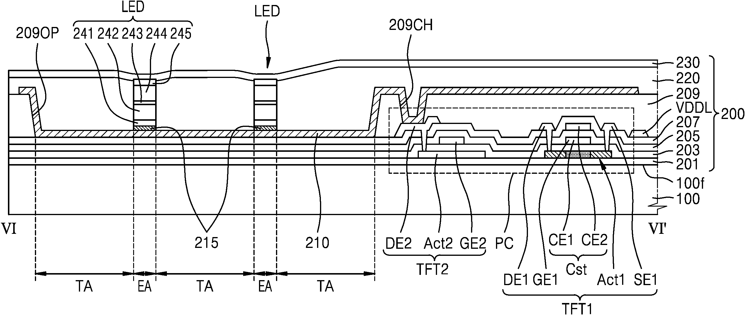
도 6을 참조하면, 기판(100) 상에 표시층(200)이 배치된다. 표시층(200)은 제1투명전극(210)과 제2투명전극(230) 사이의 발광다이오드(LED)들을 포함한다. 각 발광다이오드(LED)는 트랜지스터들을 포함하는 회로요소(PC)와 전기적으로 연결되며, 표시층(200)은 전술한 회로요소(PC)들을 포함한다. 표시층(200)은 앞서 도 2를 참조하여 설명한 바와 같이 봉지부재로 커버될 수 있으며, 도 6에서는 편의 상 봉지부재가 생략되었다.Referring to FIG. 6, a display layer (200) is arranged on a substrate (100). The display layer (200) includes light-emitting diodes (LEDs) between a first transparent electrode (210) and a second transparent electrode (230). Each light-emitting diode (LED) is electrically connected to a circuit element (PC) including transistors, and the display layer (200) includes the circuit elements (PC) described above. The display layer (200) may be covered with a sealing member as described above with reference to FIG. 2, and for convenience, the sealing member is omitted in FIG. 6.
기판(100)은 다양한 소재를 포함할 수 있다. 예를 들어, 기판(100)은 SiO2를 주성분으로 하는 투명한 유리 재질로 이루어질 수 있고, 또는, 투명 플라스틱 재질로 이루어질 수 있다. 기판(100)은 투명 플라스틱 재질로서, 가요성을 가지는 재질로 이루어질 수도 있다. 플라스틱 재질은 절연성 유기물인 폴리에테르술폰, 폴리아크릴레이트, 폴리에테르 이미드, 폴리에틸렌 나프탈레이트, 폴리에틸렌 테레프탈레이드, 폴리페닐렌 설파이드, 폴리아릴레이트, 폴리이미드, 폴리카보네이트, 셀룰로오스 트리 아세테이트, 셀룰로오스 아세테이트 프로피오네이트로 이루어진 그룹으로부터 선택되는 유기물을 포함할 수 있다.The substrate (100) may include various materials. For example, the substrate (100) may be made of a transparent glass material containing SiO 2 as a main component, or may be made of a transparent plastic material. The substrate (100) may be made of a transparent plastic material having flexibility. The plastic material may include an organic material selected from the group consisting of insulating organic materials such as polyethersulfone, polyacrylate, polyether imide, polyethylene naphthalate, polyethylene terephthalate, polyphenylene sulfide, polyarylate, polyimide, polycarbonate, cellulose triacetate, and cellulose acetate propionate.
기판(100) 상에 회로요소(PC)가 형성될 수 있다. 도 6에 도시된 바와 같이 회로요소(PC)는 기판(100) 상에 위치하 투과영역(TA)을 제외한 다른 영역 상에 배치될 수 있으며, 일 예로 회로요소(PC)는 투과영역(TA)의 일측에 배치될 수 있다. 회로요소(PC)는 제1박막트랜지스터(TFT1)와 제2박막트랜지스터(TFT2) 및 스토리지 커패시터(Cst)를 포함할 수 있다.. 회로요소(PC)가 앞서 도 3을 참조하여 설명한 바와 같은 회로구조를 갖는 경우, 도 6의 제1박막트랜지스터(TFT1)는 도 3의 제1트랜지스터에 해당하고, 제2박막트랜지스터(TFT2)는 제6트랜지스터에 해당할 수 있다.A circuit element (PC) may be formed on a substrate (100). As illustrated in FIG. 6, the circuit element (PC) may be positioned on an area other than a transparent area (TA) on the substrate (100), and for example, the circuit element (PC) may be positioned on one side of the transparent area (TA). The circuit element (PC) may include a first thin-film transistor (TFT1), a second thin-film transistor (TFT2), and a storage capacitor (Cst). When the circuit element (PC) has a circuit structure as described above with reference to FIG. 3, the first thin-film transistor (TFT1) of FIG. 6 may correspond to the first transistor of FIG. 3, and the second thin-film transistor (TFT2) may correspond to the sixth transistor.
기판(100)과 회로요소(PC) 사이에는 버퍼층(201)이 배치될 수 있다. 버퍼층(201)은 실리콘나이트라이드, 실리콘옥사이드, 또는/및 실리콘옥시나이트라이드와 같은 무기절연물을 포함할 수 있다. 버퍼층(201)은 전술한 물질을 포함하는 단일층 또는 다층 구조를 포함할 수 있다.A buffer layer (201) may be arranged between the substrate (100) and the circuit element (PC). The buffer layer (201) may include an inorganic insulating material such as silicon nitride, silicon oxide, or/and silicon oxynitride. The buffer layer (201) may include a single-layer or multi-layer structure including the aforementioned materials.
제1박막트랜지스터(TFT1) 및 제2박막트랜지스터(TFT2)는 각각 제1반도체층(Act1) 및 제2반도체층(Act2)을 포함할 수 있다. 제1반도체층(Act1) 및 제2반도체층(Act2)은 비정질 실리콘(amorphous silicon) 또는 다결정 실리콘(poly crystalline silicon)을 포함할 수 있다. 또는 제1반도체층(Act1) 및 제2반도체층(Act2)은 유기 반도체 물질 또는 산화물 반도체 물질을 포함할 수 있다. The first thin-film transistor (TFT1) and the second thin-film transistor (TFT2) may each include a first semiconductor layer (Act1) and a second semiconductor layer (Act2). The first semiconductor layer (Act1) and the second semiconductor layer (Act2) may include amorphous silicon or polycrystalline silicon. Alternatively, the first semiconductor layer (Act1) and the second semiconductor layer (Act2) may include an organic semiconductor material or an oxide semiconductor material.
제1게이트전극(GE1)은 제1반도체층(Act1)의 채널영역에 중첩하고, 제2게이트전극(GE2)은 제2반도체층(Act2)의 채널영역에 중첩할 수 있다. 제1게이트전극(GE1) 및 제2게이트전극(GE2)은 알루미늄(Al), 백금(Pt), 팔라듐(Pd), 은(Ag), 마그네슘(Mg), 금(Au), 니켈(Ni), 네오디뮴(Nd), 이리듐(Ir), 크롬(Cr), 리튬(Li), 칼슘(Ca), 몰리브덴(Mo), 티타늄(Ti), 텅스텐(W), 구리(Cu) 중 하나 이상의 물질로 단층 또는 다층으로 형성될 수 있다.The first gate electrode (GE1) may overlap the channel region of the first semiconductor layer (Act1), and the second gate electrode (GE2) may overlap the channel region of the second semiconductor layer (Act2). The first gate electrode (GE1) and the second gate electrode (GE2) may be formed as a single layer or multiple layers using one or more materials selected from the group consisting of aluminum (Al), platinum (Pt), palladium (Pd), silver (Ag), magnesium (Mg), gold (Au), nickel (Ni), neodymium (Nd), iridium (Ir), chromium (Cr), lithium (Li), calcium (Ca), molybdenum (Mo), titanium (Ti), tungsten (W), and copper (Cu).
제1게이트전극(GE1) 및 제2게이트전극(GE2), 그리고 제1반도체층(Act1) 및 제2반도체층(Act2) 사이에는 게이트절연층(203)이 배치될 수 있다. 게이트절연층(203)은 실리콘나이트라이드, 실리콘옥사이드, 또는/및 실리콘옥시나이트라이드와 같은 무기절연물을 포함할 수 있다. 게이트절연층(203)은 전술한 물질을 포함하는 단일층 또는 다층 구조를 포함할 수 있다.A gate insulating layer (203) may be arranged between the first gate electrode (GE1) and the second gate electrode (GE2), and the first semiconductor layer (Act1) and the second semiconductor layer (Act2). The gate insulating layer (203) may include an inorganic insulating material such as silicon nitride, silicon oxide, or/and silicon oxynitride. The gate insulating layer (203) may include a single-layer or multi-layer structure including the above-described material.
제1게이트전극(GE1) 및 제2게이트전극(GE2) 상에 제1층간 절연층(205)이 형성될 수 있다. 제1층간 절연층(205)은 실리콘나이트라이드, 실리콘옥사이드, 또는/및 실리콘옥시나이트라이드와 같은 무기절연물을 포함할 수 있다. 제1층간 절연층(205)은 전술한 물질을 포함하는 단일층 또는 다층 구조를 포함할 수 있다.A first interlayer insulating layer (205) may be formed on the first gate electrode (GE1) and the second gate electrode (GE2). The first interlayer insulating layer (205) may include an inorganic insulating material such as silicon nitride, silicon oxide, or/and silicon oxynitride. The first interlayer insulating layer (205) may include a single-layer or multi-layer structure including the above-described material.
스토리지 커패시터(Cst)는 중첩하는 제1전극(CE1) 및 제2전극(CE2)을 포함할 수 있다. 일부 실시예로, 제1박막트랜지스터(TFT1)의 제1게이트전극(GE1)은 스토리지 커패시터(Cst)의 제1전극(CE1)을 포함할 수 있다. 제1전극(CE1) 및 제2전극(CE2) 사이에는 제2층간 절연층(207)이 형성될 수 있다. 제2층간 절연층(207)은 실리콘나이트라이드, 실리콘옥사이드, 또는/및 실리콘옥시나이트라이드와 같은 무기절연물을 포함할 수 있다. 제2층간 절연층(207)은 전술한 물질을 포함하는 단일층 또는 다층 구조를 포함할 수 있다.The storage capacitor (Cst) may include overlapping first electrodes (CE1) and second electrodes (CE2). In some embodiments, the first gate electrode (GE1) of the first thin film transistor (TFT1) may include the first electrode (CE1) of the storage capacitor (Cst). A second interlayer insulating layer (207) may be formed between the first electrode (CE1) and the second electrode (CE2). The second interlayer insulating layer (207) may include an inorganic insulating material such as silicon nitride, silicon oxide, or/and silicon oxynitride. The second interlayer insulating layer (207) may include a single-layer or multi-layer structure including the materials described above.
제2층간 절연층(207) 상에 제1소스전극(SE1) 및 제1드레인전극(DE1)이 형성될 수 있다. 유사하게, 제2소스 또는 드레인 전극이 형성될 수 있으며, 도 6은 제2드레인전극(DE2)을 도시한다.A first source electrode (SE1) and a first drain electrode (DE1) may be formed on the second interlayer insulating layer (207). Similarly, a second source or drain electrode may be formed, and FIG. 6 illustrates a second drain electrode (DE2).
제1소스전극(SE1) 및 제1드레인전극(DE1), 제2드레인전극(DE2), 및 제1전원전압라인(VDDL)은 앞서 도 5a를 참조하여 설명한 제1 내지 제3데이터라인(DL1, DL2, DL3), 또는/및 제2전원전압라인(VSSL, 도 5a, 도 5b)과 동일한 층 상에 위치하며, 동일한 물질을 포함할 수 있다. The first source electrode (SE1) and the first drain electrode (DE1), the second drain electrode (DE2), and the first power voltage line (VDDL) are positioned on the same layer as the first to third data lines (DL1, DL2, DL3) and/or the second power voltage line (VSSL, FIGS. 5a and 5b) described above with reference to FIG. 5a, and may include the same material.
제1소스전극(SE1) 및 제1드레인전극(DE1), 그리고 제2드레인전극(DE2)은 알루미늄(Al), 백금(Pt), 팔라듐(Pd), 은(Ag), 마그네슘(Mg), 금(Au), 니켈(Ni), 네오디뮴(Nd), 이리듐(Ir), 크롬(Cr), 리튬(Li), 칼슘(Ca), 몰리브덴(Mo), 티타늄(Ti), 텅스텐(W), 구리(Cu)와 같은 물질을 포함할 수 있으며, 전술한 물질을 포함하는 단일층 또는 다층 구조를 포함할 수 있다. The first source electrode (SE1), the first drain electrode (DE1), and the second drain electrode (DE2) may include materials such as aluminum (Al), platinum (Pt), palladium (Pd), silver (Ag), magnesium (Mg), gold (Au), nickel (Ni), neodymium (Nd), iridium (Ir), chromium (Cr), lithium (Li), calcium (Ca), molybdenum (Mo), titanium (Ti), tungsten (W), and copper (Cu), and may include a single-layer or multi-layer structure including the aforementioned materials.
회로요소(PC)는 유기절연층(209)으로 커버될 수 있다. 유기절연층(209)은 Polymethylmethacrylate(PMMA)나, Polystylene(PS)과 같은 일반 범용고분자, 페놀계 그룹을 갖는 고분자 유도체, 아크릴계 고분자, 이미드계 고분자, 아릴에테르계 고분자, 아마이드계 고분자, 불소계고분자, p-자일렌계 고분자, 비닐알콜계 고분자 및 이들의 블렌드 등을 포함할 수 있다. The circuit element (PC) may be covered with an organic insulating layer (209). The organic insulating layer (209) may include a general-purpose polymer such as polymethylmethacrylate (PMMA) or polystylene (PS), a polymer derivative having a phenol group, an acrylic polymer, an imide polymer, an aryl ether polymer, an amide polymer, a fluorinated polymer, a p-xylene polymer, a vinyl alcohol polymer, and blends thereof.
유기절연층(209)은 회로요소(PC)와 제1투명전극(210)의 전기적 연결을 위한 콘택홀(209CH) 및 콘택홀(209CH)과 상호 이격된 개구(209OP)를 포함할 수 있다.The organic insulating layer (209) may include a contact hole (209CH) for electrical connection between the circuit element (PC) and the first transparent electrode (210) and an opening (209OP) spaced apart from the contact hole (209CH).
제1투명전극(210)은 개구(209OP) 및 콘택홀(209CH)을 커버할 수 있다. 제1투명전극(210)의 일 부분(예, 대부분)은 유기절연층(209)의 개구(209OP)에 위치하며, 제1투명전극(210)의 다른 부분은 유기절연층(209)의 상면 상에 위치할 수 있으며, 제1투명전극(210)은 콘택홀(209CH)을 통해 회로요소(PC)와 전기적으로 연결될 수 있다. 제1투명전극(210)의 대부분(예컨대, 제1투명전극의 약 50%이상의 면적을 갖는 부분, 보다 바람직하게 약 60% 이상이거나 약 70%이상의 면적을 갖는 부분)은 유기절연층(209)의 개구(209OP)에 위치할 수 있다. 제1투명전극(210)의 제1에지는 개구(209OP)를 정의하는 유기절연층(209)의 측면을 지나 유기절연층(209)의 상면 상에 위치할 수 있다. The first transparent electrode (210) can cover the opening (209OP) and the contact hole (209CH). A part (e.g., most) of the first transparent electrode (210) can be positioned in the opening (209OP) of the organic insulating layer (209), and another part of the first transparent electrode (210) can be positioned on the upper surface of the organic insulating layer (209), and the first transparent electrode (210) can be electrically connected to the circuit element (PC) through the contact hole (209CH). A most part of the first transparent electrode (210) (e.g., a part having an area of about 50% or more of the first transparent electrode, more preferably, a part having an area of about 60% or more or about 70% or more) can be positioned in the opening (209OP) of the organic insulating layer (209). The first edge of the first transparent electrode (210) may be positioned on the upper surface of the organic insulating layer (209) past the side of the organic insulating layer (209) defining the opening (209OP).
제1투명전극(210)은 투명 도전성 산화물을 포함할 수 있다. 일부 실시예로서, 제1투명전극(210)은 다결정의 투명 도전성 산화물을 포함할 수 있다. 예컨대, 제1투명전극(210)은 다결정의 인듐틴옥사이드(polycrystalline ITO)를 포함할 수 있다. 또는, 제1투명전극(210)은 다결정의 인듐징크옥사이드(IZO; indium zinc oxide), 징크옥사이드(ZnO; zinc oxide), 인듐옥사이드(In2O3; indium oxide), 인듐갈륨옥사이드(IGO; indium gallium oxide) 및 알루미늄징크옥사이드(AZO; aluminum zinc oxide)등을 포함할 수 있다. The first transparent electrode (210) may include a transparent conductive oxide. In some embodiments, the first transparent electrode (210) may include a polycrystalline transparent conductive oxide. For example, the first transparent electrode (210) may include polycrystalline indium tin oxide (ITO). Alternatively, the first transparent electrode (210) may include polycrystalline indium zinc oxide (IZO), zinc oxide (ZnO), indium oxide (In 2 O 3 ), indium gallium oxide (IGO), aluminum zinc oxide (AZO), etc.
발광다이오드(LED)는 제1투명전극(210) 상에 위치한다. 일부 실시예에서, 적어도 하나의 발광다이오드(LED)는 유기절연층(209)의 개구(209OP)와 중첩하는 제1투명전극(210) 상에 위치할 수 있다. 일 실시예로서, 도 6은 두 개의 발광다이오드(LED)들이 제1투명전극(210) 상에 위치하되, 유기절연층(209)의 개구(209OP)와 중첩하게 배치될 수 있다. A light emitting diode (LED) is positioned on the first transparent electrode (210). In some embodiments, at least one light emitting diode (LED) may be positioned on the first transparent electrode (210) overlapping an opening (209OP) of an organic insulating layer (209). As an example, FIG. 6 illustrates that two light emitting diodes (LEDs) may be positioned on the first transparent electrode (210) so as to overlap an opening (209OP) of an organic insulating layer (209).
발광다이오드(LED)는 제1반도체층(242), 제2반도체층(244) 및, 제1반도체층(242)과 제2반도체층(244) 사이의 활성층(243)을 포함할 수 있다.A light-emitting diode (LED) may include a first semiconductor layer (242), a second semiconductor layer (244), and an active layer (243) between the first semiconductor layer (242) and the second semiconductor layer (244).
제1반도체층(242)은 예를 들어, p형 반도체층으로 구현될 수 있다. 제1반도체층(242)은 InxAlyGa1 -x- yN (0x≤1, 0≤y≤1, 0≤x+y≤1)의 조성식을 갖는 반도체 재료, 예를 들어 GaN, AlN, AlGaN, InGaN, InN, InAlGaN, AlInN 등에서 선택될 수 있으며, Mg, Zn, Ca, Sr, Ba 등의 p형 도펀트가 도핑될 수 있다.The first semiconductor layer (242) can be implemented as a p-type semiconductor layer, for example. The first semiconductor layer (242) is In x Al y Ga 1 -x- y N (0 The semiconductor material having a composition formula of x≤1, 0≤y≤1, 0≤x+y≤1 can be selected from, for example, GaN, AlN, AlGaN, InGaN, InN, InAlGaN, AlInN, etc., and can be doped with a p-type dopant such as Mg, Zn, Ca, Sr, Ba, etc.
제2반도체층(244)은 예를 들어, n형 반도체층일 수 있다. 제2반도체층(244)은 InxAlyGa1 -x- yN (0x≤1, 0≤y≤1, 0≤x+y≤1)의 조성식을 갖는 반도체 재료, 예를 들어 GaN, AlN, AlGaN, InGaN, InN, InAlGaN, AlInN 등에서 선택될 수 있으며, Si, Ge, Sn 등의 n형 도펀트가 도핑될 수 있다.The second semiconductor layer (244) may be, for example, an n-type semiconductor layer. The second semiconductor layer (244) may be In x Al y Ga 1 -x- y N (0 The semiconductor material having a composition formula of x≤1, 0≤y≤1, 0≤x+y≤1 can be selected from, for example, GaN, AlN, AlGaN, InGaN, InN, InAlGaN, AlInN, etc., and can be doped with an n-type dopant such as Si, Ge, or Sn.
제1반도체층(242), 제2반도체층(244)의 도핑 타입은 예시적인 것으로 이에 한하지 않으며, 제1반도체층(242)이 n형 반도체층이고, 제2반도체층(244)이 p형 반도체층이 될 수도 있다. The doping types of the first semiconductor layer (242) and the second semiconductor layer (244) are exemplary and are not limited thereto, and the first semiconductor layer (242) may be an n-type semiconductor layer and the second semiconductor layer (244) may be a p-type semiconductor layer.
활성층(243)은 전자와 정공이 재결합되는 영역으로, 전자와 정공이 재결합함에 따라 낮은 에너지 준위로 천이하며, 그에 상응하는 파장을 가지는 빛을 생성할 수 있다. 활성층(243)은 예를 들어, InxAlyGa1 -x- yN (0x≤1, 0≤y≤1, 0≤x+y≤1)의 조성식을 가지는 반도체 재료를 포함하여 형성할 수 있으며, 단일 양자 우물 구조 또는 다중 양자 우물 구조(MQW: Multi Quantum Well)로 형성될 수 있다. 또한, 양자선(Quantum wire)구조 또는 양자점(Quantum dot)구조를 포함할 수도 있다. The active layer (243) is a region where electrons and holes recombine, and as electrons and holes recombine, they transition to a lower energy level and can generate light having a corresponding wavelength. The active layer (243) is, for example, In x Al y Ga 1 -x- y N (0 It can be formed by including a semiconductor material having a composition formula of x≤1, 0≤y≤1, 0≤x+y≤1), and can be formed as a single quantum well structure or a multi-quantum well structure (MQW: Multi Quantum Well). In addition, it may include a quantum wire structure or a quantum dot structure.
발광다이오드(LED)는 수직형(vertical type)으로, 제1전극패드(241)와 제2전극패드(245)가 제1반도체층(242), 활성층(243), 제2반도체층(244)의 적층 방향을 따라 상호 이격될 수 있다. 제1전극패드(241)와 제2전극패드(245)가 서로 반대 방향을 향해 노출될 수 있다. 발광다이오드(LED)가 플립 타입, 예컨대 제1전극패드와 제2전극패드가 동일한 면을 향해 노출된 경우, 제1 및 제2 전극패드들 및 이들에 각각에 소정의 전압을 인가하기 위한 전극들을 접속시켜야 하므로 얼라인 공정이 어렵고, 수직형의 발광다이오드(LED) 보다 폭이 커지므로 그만큼 투과영역(TA)이 감소할 수 있다. 그러나, 수직형 발광다이오드는 수직형 발광다이오드(LED)의 얼라인 공정이 간단하며 제1투명전극(210) 상에서 발광다이오드(LED)가 차지하는 면적이 상대적으로 작기 때문에 투과영역(TA)의 면적을 증가시킬 수 있는 장점이 있다. 따라서, 발광다이오드(LED)는 수직형 발광다이오드를 포함하는 것이 더 바람직할 수 있다.The light emitting diode (LED) is of a vertical type, and the first electrode pad (241) and the second electrode pad (245) can be spaced apart from each other along the lamination direction of the first semiconductor layer (242), the active layer (243), and the second semiconductor layer (244). The first electrode pad (241) and the second electrode pad (245) can be exposed in opposite directions. If the light emitting diode (LED) is of a flip type, for example, the first electrode pad and the second electrode pad are exposed toward the same surface, the first and second electrode pads and the electrodes for applying a predetermined voltage to each of them must be connected, so the alignment process is difficult, and since the width is larger than that of a vertical light emitting diode (LED), the transmittance area (TA) can be reduced accordingly. However, vertical light-emitting diodes have the advantage of being able to increase the area of the transmission area (TA) because the alignment process of the vertical light-emitting diode (LED) is simple and the area occupied by the light-emitting diode (LED) on the first transparent electrode (210) is relatively small. Therefore, it may be more preferable for the light-emitting diode (LED) to include a vertical light-emitting diode.
발광다이오드(LED)의 제1전극패드(241) 및 제2전극패드(245)는 금속을 포함할 수 있다. 일 실시예로, 제1전극패드(241) 및 제2전극패드(245)는 주석(Sn), 은(Ag), 구리(Cu) 및/또는 이들의 합금을 포함할 수 있다. 제1전극패드(241) 및 제2전극패드(245)는 서로 동일한 물질을 포함하거나, 서로 다른 물질을 포함할 수 있다. 일부 실시예로서, 제1전극패드(241) 및 제2전극패드(245)는 주석(Sn)의 함량이 제일 많고, 은(Ag), 구리(Cu)의 순서로 함량이 줄어드는 합금을 포함할 수 있다. The first electrode pad (241) and the second electrode pad (245) of the light emitting diode (LED) may include a metal. In one embodiment, the first electrode pad (241) and the second electrode pad (245) may include tin (Sn), silver (Ag), copper (Cu), and/or an alloy thereof. The first electrode pad (241) and the second electrode pad (245) may include the same material or different materials. In some embodiments, the first electrode pad (241) and the second electrode pad (245) may include an alloy in which the content of tin (Sn) is the highest and the content of silver (Ag) and copper (Cu) decrease in that order.
제1전극패드(241)는 제1투명전극(210)과 전기적으로 연결되고, 제2전극패드(245)는 제2투명전극(230)과 전기적으로 연결될 수 있다. 제1전극패드(241)와 제1투명전극(210) 사이에는 점착층(215)이 배치될 수 있다. 점착층(215)은 발광다이오드(LED)에만 중첩할 수 있다. 점착층(215)은 발광다이오드(LED)와 대응하는 면적을 가질 수 있다. 예컨대, 기판(100)의 상면에 수직한 방향에서 발광다이오드(LED)를 사영하였을 때 발광다이오드(LED)의 면적과 점착층(215)의 면적이 실질적으로 동일할 수 있다. 여기서, A와 B의 면적이 실질적으로 동일하다고 함은 A의 면적과 B의 면적의 차이가 A 또는 B의 10% 보다 작은 경우일 수 있다. 보다 바람직하게는 A의 면적과 B의 면적의 차이가 약 8%보다 작거나 약 5% 보다 작을 수 있다. The first electrode pad (241) may be electrically connected to the first transparent electrode (210), and the second electrode pad (245) may be electrically connected to the second transparent electrode (230). An adhesive layer (215) may be arranged between the first electrode pad (241) and the first transparent electrode (210). The adhesive layer (215) may only overlap a light-emitting diode (LED). The adhesive layer (215) may have an area corresponding to the light-emitting diode (LED). For example, when the light-emitting diode (LED) is projected in a direction perpendicular to the upper surface of the substrate (100), the area of the light-emitting diode (LED) and the area of the adhesive layer (215) may be substantially the same. Here, the areas of A and B being substantially the same may mean that the difference between the area of A and the area of B is less than 10% of A or B. More preferably, the difference between the area of A and the area of B may be less than about 8% or less than about 5%.
점착층(215)은 금속을 포함할 수 있다. 점착층(215)은 구리(Cu), 은(Ag), 및 금(Au)에서 선택된 적어도 하나 이상의 금속원소를 포함할 수 있다. 일 실시예로, 점착층(215)은 전술한 물질을 포함하는 단일층이거나 다층 구조를 포함할 수 있다. The adhesive layer (215) may include a metal. The adhesive layer (215) may include at least one metal element selected from copper (Cu), silver (Ag), and gold (Au). In one embodiment, the adhesive layer (215) may be a single layer including the above-described material or may include a multilayer structure.
제2투명전극(230)은 인듐틴옥사이드(ITO; indium tin oxide), 인듐징크옥사이드(IZO; indium zinc oxide), 징크옥사이드(ZnO; zinc oxide), 인듐옥사이드(In2O3; indium oxide), 인듐갈륨옥사이드(IGO; indium gallium oxide) 및 알루미늄징크옥사이드(AZO; aluminum zinc oxide)와 같은 전도성 산화물 중 어느 하나 이상을 구비할 수 있다. 제2투명전극(230)은 앞서 도 5a 또는 도 5b를 참조하여 설명한 제2전원전압라인(VSSL, 도 5a또는 도 5b)과 전기적으로 연결될 수 있다. 제2전원전압라인(VSSL, 도 5a또는 도 5b)은 제1소스전극(SE) 또는 제1드레인전극(DE1)과 동일한 층 상에 형성되거나, 제1투명전극(210)과 동일한 층 상에 형성될 수 있다. 제2투명전극(230)과 제2전원전압라인(VSSL)의 전기적 연결을 위하여 이들 사이에 위치하는 절연층들, 예컨대 유기절연층(209) 및/또는 투명 절연층(220)은 각각 콘택홀을 포함할 수 있다.The second transparent electrode (230) may include at least one of conductive oxides such as indium tin oxide (ITO), indium zinc oxide (IZO), zinc oxide (ZnO), indium oxide (In 2 O 3 ), indium gallium oxide (IGO), and aluminum zinc oxide (AZO). The second transparent electrode (230) may be electrically connected to the second power supply voltage line (VSSL, FIG. 5a or FIG. 5b) described above with reference to FIG. 5a or FIG. 5b. The second power supply voltage line (VSSL, FIG. 5a or FIG. 5b) may be formed on the same layer as the first source electrode (SE) or the first drain electrode (DE1), or may be formed on the same layer as the first transparent electrode (210). In order to electrically connect the second transparent electrode (230) and the second power voltage line (VSSL), the insulating layers positioned between them, such as the organic insulating layer (209) and/or the transparent insulating layer (220), may each include a contact hole.
제1투명전극(210)이 앞서 도 5a를 참조하여 설명한 바와 같이 이웃한 제1투명전극(210)과 상호 이격되도록 배치된 것과 달리, 제2투명전극(230)은 기판(100)을 전체적으로 커버하도록 일체(一體, one body)로 형성될 수 있다. 예컨대, 제2투명전극(230)은 표시영역을 커버하도록 일체로 형성될 수 있다. Unlike the first transparent electrode (210) which is arranged to be spaced apart from the adjacent first transparent electrode (210) as described above with reference to FIG. 5a, the second transparent electrode (230) may be formed as one body to cover the entire substrate (100). For example, the second transparent electrode (230) may be formed as one body to cover the display area.
제1투명전극(210)과 제2투명전극(230) 사이에는 투명 절연층(220)이 개재될 수 있다. 투명 절연층(220)은 발광다이오드(LED)의 측면을 둘러쌀 수 있으며, 발광다이오드(LED)의 측면과 직접 접촉할 수 있다.A transparent insulating layer (220) may be interposed between the first transparent electrode (210) and the second transparent electrode (230). The transparent insulating layer (220) may surround the side of the light-emitting diode (LED) and may be in direct contact with the side of the light-emitting diode (LED).
투명 절연층(220)은 투명 유기물을 포함할 수 있다. 투명 절연층(220)은 예컨대, 아크릴, 폴리(메틸 메타크릴레이트)(PMMA), 벤조사이클로부텐(BCB), 폴리이미드, 아크릴레이트, 에폭시 및 폴리에스테르 등과 같은 유기물을 포함할 수 있다.The transparent insulating layer (220) may include a transparent organic material. The transparent insulating layer (220) may include an organic material such as, for example, acrylic, poly(methyl methacrylate) (PMMA), benzocyclobutene (BCB), polyimide, acrylate, epoxy, and polyester.
도 6에 도시된 바와 같이 투과영역(TA)은 발광영역(EA)과 인접하게 배치된다. 발광영역(EA)에 발광다이오드(LED)가 배치된 것과 달리 투과영역(TA)에는 발광다이오드(LED)가 존재하지 않는다. As illustrated in Fig. 6, the transparent area (TA) is positioned adjacent to the emitting area (EA). Unlike the emitting area (EA) where a light-emitting diode (LED) is positioned, the transparent area (TA) does not have a light-emitting diode (LED).
투과영역(TA) 및 적어도 어느 하나의 발광영역(EA)은 유기절연층(209)의 개구(209OP)와 중첩할 수 있다. 투과영역(TA)은, 제1투명전극(210) 및 제2투명전극(230)과 중첩할 수 있으며, 제1투명전극(210) 및 제2투명전극(230) 사이의 투명 절연층(220)과 중첩할 수 있다. 예컨대, 투과영역(TA)은 순차적으로 적층된 제1투명전극(210), 투명 절연층(220), 및 제2투명전극(230)의 적층 구조와 중첩할 수 있다. 투명 절연층(220)은 투과영역(TA)에서 제1투명전극(210) 및 제2투명전극(230)에 직접 접촉할 수 있다. The transparent area (TA) and at least one of the light-emitting areas (EA) can overlap with the opening (209OP) of the organic insulating layer (209). The transparent area (TA) can overlap with the first transparent electrode (210) and the second transparent electrode (230), and can overlap with the transparent insulating layer (220) between the first transparent electrode (210) and the second transparent electrode (230). For example, the transparent area (TA) can overlap with a laminated structure of the first transparent electrode (210), the transparent insulating layer (220), and the second transparent electrode (230) that are sequentially laminated. The transparent insulating layer (220) can be in direct contact with the first transparent electrode (210) and the second transparent electrode (230) in the transparent area (TA).
기판(100)의 전면(또는 주면, 100f)에 수직한 방향에서 보았을 때, 예컨대 평면상에서, 투과영역(TA)은 앞서 도 4를 참조하여 설명한 바와 같이 발광영역(EA)을 전체적으로 둘러쌀 수 있다. 도 5a 또는 도 5b, 그리고 도 6을 참조하여 설명한 구조를 갖는 표시 장치에서, 표시영역은 도 4의 단위(U)들이 반복적으로 배치된 2차원 배열 구조를 포함할 수 있다. 전술한 구조를 갖는 경우, 각 단위(U)에서의 투과영역(TA)이 차지하는 면적은 각 단위(U)의 면적의 약 50% 이상일 수 있다.When viewed in a direction perpendicular to the front surface (or main surface, 100f) of the substrate (100), for example, in a plane, the transmission area (TA) can entirely surround the emission area (EA) as described above with reference to FIG. 4. In the display device having the structure described with reference to FIG. 5a or FIG. 5b, and FIG. 6, the display area can include a two-dimensional array structure in which the units (U) of FIG. 4 are repeatedly arranged. In the case of having the above-described structure, the area occupied by the transmission area (TA) in each unit (U) can be about 50% or more of the area of each unit (U).
도 7a는 본 발명의 일 실시예에 따른 표시 장치의 제조 공정에 따른 단면도이고, 도 7b는 본 발명의 일 실시예에 따른 표시 장치의 제조 공정에 따른 평면도이다.FIG. 7a is a cross-sectional view according to a manufacturing process of a display device according to one embodiment of the present invention, and FIG. 7b is a plan view according to a manufacturing process of a display device according to one embodiment of the present invention.
도 7a 및 도 7b를 참조하면, 기판(100) 상에 회로요소(PC)를 형성할 수 있으며, 회로요소(PC)는 전술한 바와 같이 제1 및 제2박막트랜지스터(TFT1, TFT2)와 스토리지 커패시터(Cst)를 포함할 수 있다. 회로요소(PC)를 형성하기 전에, 그리고 회로요소(PC)를 형성하는 공정 중에 버퍼층(201), 게이트절연층(203), 제1층간 절연층(205), 제2층간 절연층(207)을 형성할 수 있으며, 그 구체적 물질은 앞서 설명한 바와 같다. 회로요소(PC) 상에 유기절연층(209)을 형성하고, 유기절연층(209)의 일부를 제거함으로써 콘택홀(209CH) 및 개구(209OP)를 형성할 수 있다. Referring to FIGS. 7a and 7b, a circuit element (PC) can be formed on a substrate (100), and the circuit element (PC) can include first and second thin-film transistors (TFT1, TFT2) and a storage capacitor (Cst) as described above. Before forming the circuit element (PC), and during the process of forming the circuit element (PC), a buffer layer (201), a gate insulating layer (203), a first interlayer insulating layer (205), and a second interlayer insulating layer (207) can be formed, and the specific materials thereof are as described above. An organic insulating layer (209) can be formed on the circuit element (PC), and a contact hole (209CH) and an opening (209OP) can be formed by removing a part of the organic insulating layer (209).
회로요소(PC)를 형성하는 공정에서, 신호라인들 및 전원라인들이 형성될 수 있다. 예컨대, 도 7b에 도시된 스캔라인(SWL), 이전스캔라인(SIL), 발광제어라인(EL), 초기화전압라인(VL), 제1 내지 제3데이터라인(DL1, DL2, DL3), 제1전원전압라인(VDDL), 및/또는 제2전원전압라인(VSSL)이 형성될 수 있다. 일부 실시예에서, 스캔라인(SWL), 이전스캔라인(SIL), 및 발광제어라인(EL)은 제1박막트랜지스터(TFT1)의 게이트전극과 동일한 층 상에 위치하며 동일한 물질로 형성될 수 있다. 초기화전압라인(VL)은 스토리지 커패시터(Cst)의 제2전극(CE2)과 동일한 층 상에 위치하며 동일한 물질로 형성될 수 있다. 제1 내지 제3데이터라인(DL1, DL2, DL3), 제1전원전압라인(VDDL), 및/또는 제2전원전압라인(VSSL)은 제1박막트랜지스터(TFT1)의 제1소스전극(SE1) 또는 제1드레인전극(DE1)과 동일한 층 상에 위치하며 동일한 물질로 형성될 수 있다. 일 부 실시예에서, 제2전원전압라인(VSSL)은 후술할 제1투명전극(210)과 동일한 층 상에 위치하며 동일한 물질로 형성될 수 있다.In a process of forming a circuit element (PC), signal lines and power lines may be formed. For example, a scan line (SWL), a previous scan line (SIL), an emission control line (EL), an initialization voltage line (VL), first to third data lines (DL1, DL2, DL3), a first power voltage line (VDDL), and/or a second power voltage line (VSSL) illustrated in FIG. 7b may be formed. In some embodiments, the scan line (SWL), the previous scan line (SIL), and the emission control line (EL) may be positioned on the same layer as a gate electrode of the first thin film transistor (TFT1) and formed of the same material. The initialization voltage line (VL) may be positioned on the same layer as a second electrode (CE2) of the storage capacitor (Cst) and formed of the same material. The first to third data lines (DL1, DL2, DL3), the first power voltage line (VDDL), and/or the second power voltage line (VSSL) may be positioned on the same layer as the first source electrode (SE1) or the first drain electrode (DE1) of the first thin film transistor (TFT1) and may be formed of the same material. In some embodiments, the second power voltage line (VSSL) may be positioned on the same layer as the first transparent electrode (210) to be described later and may be formed of the same material.
다음으로, 제1투명전극(210) 및 제1투명전극(210) 상의 금속층(215P)을 형성한다. 제1투명전극(210)은 투명 도전성 산화물층을 형성한 후, 투명 도전성 산화물층을 폴리화하여 형성할 수 있다. 일부 실시예로서, 투명 도전성 산화물층에 고온을 가하는 경우, 다결정의 투명 도전성 산화물층, 예컨대 다결정의 ITO를 포함하는 제1투명전극(210)을 형성할 수 있다.Next, the first transparent electrode (210) and the metal layer (215P) on the first transparent electrode (210) are formed. The first transparent electrode (210) can be formed by forming a transparent conductive oxide layer and then poly-forming the transparent conductive oxide layer. In some embodiments, when a high temperature is applied to the transparent conductive oxide layer, the first transparent electrode (210) including a polycrystalline transparent conductive oxide layer, for example, polycrystalline ITO, can be formed.
이 후, 금속층(215P)을 형성할 수 있다. 금속층(215P)은 구리(Cu), 은(Ag), 및 금(Au)에서 선택된 하나 이상의 금속원소를 포함할 수 있다. 일부 실시예에서, 금속층(215P)은 구리층일 수 있다.After this, a metal layer (215P) can be formed. The metal layer (215P) can include one or more metal elements selected from copper (Cu), silver (Ag), and gold (Au). In some embodiments, the metal layer (215P) can be a copper layer.
도 8a 및 도 8b는 각각 본 발명의 일 실시예에 따른 표시 장치의 제조 공정에 따른 단면도이고, 도 8c는 본 발명의 일 실시예에 따른 표시 장치의 제조 공정에 따른 평면도이다.FIGS. 8A and 8B are cross-sectional views illustrating a manufacturing process of a display device according to one embodiment of the present invention, respectively, and FIG. 8C is a plan view illustrating a manufacturing process of a display device according to one embodiment of the present invention.
도 8a를 참조하면, 금속층(215P) 상에 발광다이오드(LED)들을 배치 또는 배열할 수 있다. 예컨대, 발광다이오드(LED)들은 공용 접합(eutectic bonding)될 수 있다. 금속층(215P)이 제1투명전극(210)과 중첩하며 제1투명전극(210)과 실질적으로 동일한 면적을 가지므로, 발광다이오드(LED)를 실장하는 공정, 예컨대 발광다이오드(LED)를 얼라인하는 공정을 비교적 간단하고 용이하게 수행할 수 있다.Referring to FIG. 8a, light emitting diodes (LEDs) can be arranged or placed on the metal layer (215P). For example, the light emitting diodes (LEDs) can be eutectic bonded. Since the metal layer (215P) overlaps the first transparent electrode (210) and has substantially the same area as the first transparent electrode (210), a process of mounting the light emitting diodes (LEDs), for example, a process of aligning the light emitting diodes (LEDs), can be performed relatively simply and easily.
다음으로, 발광다이오드(LED)를 마스크로 이용하여 금속층(215P)을 제거함으로써, 발광다이오드(LED)와 제1투명전극(210) 사이에 점착층(215)이 형성될 수 있다. 금속층(215P)은 습식 또는 건식 식각을 통해 제거될 수 있으며, 식각 공정을 통해 제1투명전극(210)과 발광다이오드(LED) 사이에만 점착층(215)이 배치될 수 있다. 제1투명전극(210)이 다결정의 투명 도전성 물질을 포함하기에, 식각 공정에서 제1투명전극(210)의 손상을 최소화하거나 방지할 수 있다.Next, by removing the metal layer (215P) using the light emitting diode (LED) as a mask, an adhesive layer (215) can be formed between the light emitting diode (LED) and the first transparent electrode (210). The metal layer (215P) can be removed through wet or dry etching, and the adhesive layer (215) can be arranged only between the first transparent electrode (210) and the light emitting diode (LED) through the etching process. Since the first transparent electrode (210) includes a polycrystalline transparent conductive material, damage to the first transparent electrode (210) can be minimized or prevented during the etching process.
전술한 공정들을 통해 각각의 제1투명전극(210) 상에는 도 8c에 도시된 바와 같이 복수의 발광다이오드(LED)들이 배치될 수 있다. 도 8c는 일 실시예로서, 각각의 제1투명전극(210) 상에서 발광다이오드(LED)들이 동일한 간격으로 배치된 것을 도시한다.Through the processes described above, a plurality of light-emitting diodes (LEDs) can be arranged on each first transparent electrode (210), as shown in FIG. 8c. FIG. 8c illustrates, as an example, that light-emitting diodes (LEDs) are arranged at equal intervals on each first transparent electrode (210).
도 9a는 본 발명의 일 실시예에 따른 표시 장치의 제조 공정에 따른 단면도이고, 도 9b는 본 발명의 일 실시예에 따른 표시 장치의 제조 공정에 따른 평면도이다.FIG. 9a is a cross-sectional view according to a manufacturing process of a display device according to one embodiment of the present invention, and FIG. 9b is a plan view according to a manufacturing process of a display device according to one embodiment of the present invention.
도 9a를 참조하면, 발광다이오드(LED)들을 배치한 후 순차적으로 투명 절연층(220) 및 제2투명전극(230)을 형성한다. 투명 절연층(220) 및 제2투명전극(230)은 기판(100)을 전체적으로 커버하도록 일체로 형성될 수 있다. 또는, 투명 절연층(220)은 도 9b에 도시된 세 개의 제1투명전극(210)들과 중첩할 수 있는 면적을 가질 수 있으며, 아일랜드 타입으로 각 단위(U)마다 배치될 수 있다. 이 경우, 어느 하나의 단위(U)의 투명 절연층(220)은 인접한 다른 하나의 단위(U)의 투명 절연층(220)과 이격될 수 있다.Referring to FIG. 9a, after arranging light-emitting diodes (LEDs), a transparent insulating layer (220) and a second transparent electrode (230) are sequentially formed. The transparent insulating layer (220) and the second transparent electrode (230) may be formed integrally to cover the entire substrate (100). Alternatively, the transparent insulating layer (220) may have an area that can overlap with the three first transparent electrodes (210) illustrated in FIG. 9b, and may be arranged in an island type for each unit (U). In this case, the transparent insulating layer (220) of one unit (U) may be spaced apart from the transparent insulating layer (220) of another adjacent unit (U).
도 10은 본 발명의 일 실시예에 따른 표시 장치의 일부를 나타낸 평면도이다.FIG. 10 is a plan view showing a part of a display device according to one embodiment of the present invention.
도 10을 참조하면, 단위(U)는 앞서 도 4를 참조하여 설명한 바와 같이 제1방향(예, y방향)으로 연장된 복수의 수직라인들과 제2방향(예, x방향)으로 연장된 복수의 수평라인들을 포함할 수 있다. 복수의 수직라인들은 예컨대 제1 내지 제3데이터라인(DL1, DL2, DL3), 제1전원전압라인(VDDL), 및 제2전원전압라인(VSSL)을 포함할 수 있다. 복수의 수평라인들은 예컨대 스캔라인(SWL), 이전스캔라인(SIL), 발광제어라인(EL), 및 초기화전압라인(VL)을 포함할 수 있다.Referring to FIG. 10, a unit (U) may include a plurality of vertical lines extending in a first direction (e.g., y direction) and a plurality of horizontal lines extending in a second direction (e.g., x direction) as described above with reference to FIG. 4. The plurality of vertical lines may include, for example, first to third data lines (DL1, DL2, DL3), a first power voltage line (VDDL), and a second power voltage line (VSSL). The plurality of horizontal lines may include, for example, a scan line (SWL), a previous scan line (SIL), an emission control line (EL), and an initialization voltage line (VL).
앞서 도 5a에 도시된 바와 같이 단위(U)에서 발광다이오드(LED, 도 5a)들이 제1투명전극(210, 도 5a) 상에서 제1방향을 따라 일정한 간격을 가지도록 상호 이격되어 배치되며, 따라서 도 4에 도시된 바와 같이 적색의 발광영역(EA)들이 제1방향을 따라 일정한 간격을 가지도록 배치되고, 녹색의 발광영역(EA-G) 및 청색의 발광영역(EA-B)도 마찬가지로 제1방향을 따라 일정한 간격을 가지도록 배치된 것을 설명하였다. 다른 실시예로, 도 10에 도시된 바와 같이 발광영역들은 제1투명전극(210)의 일 부분 상에 치우쳐서(오프셋되어) 배치될 수 있다. As previously illustrated in FIG. 5a, light emitting diodes (LEDs, FIG. 5a) in a unit (U) are arranged so as to be spaced apart from each other at a constant interval along a first direction on a first transparent electrode (210, FIG. 5a), and thus, as illustrated in FIG. 4, red light emitting areas (EA) are arranged at a constant interval along the first direction, and green light emitting areas (EA-G) and blue light emitting areas (EA-B) are also arranged at constant intervals along the first direction. In another embodiment, as illustrated in FIG. 10, the light emitting areas may be arranged offset from each other on a portion of the first transparent electrode (210).
일부 실시예로서, 적색의 발광영역(EA-R)들은 제1투명전극(210) 상에 위치하되, 도 10에 도시된 제1투명전극(210)의 아래쪽 부분 상에 배치될 수 있다. 유사하게, 녹색의 발광영역(EA-G)들 및 청색의 발광영역(EA-B)들도 각각 해당하는 제1투명전극(210) 상에 위치하되, 도 10에 도시된 제1투명전극(210)의 아래쪽 부분 상에 배치될 수 있다.In some embodiments, the red light-emitting regions (EA-R) may be positioned on the first transparent electrode (210), but may be positioned on the lower portion of the first transparent electrode (210) as illustrated in FIG. 10. Similarly, the green light-emitting regions (EA-G) and the blue light-emitting regions (EA-B) may also be positioned on the corresponding first transparent electrode (210), but may be positioned on the lower portion of the first transparent electrode (210) as illustrated in FIG. 10.
도 10에서 발광영역의 위치는 발광다이오드의 위치에 해당할 수 있다. 도 10에서 적색의 발광영역(EA-R)들 각각은 적색의 빛을 방출하는 발광다이오드의 위치에 해당하고, 녹색의 발광영역(EA-G)들 각각은 녹색의 빛을 방출하는 발광다이오드의 위치에 해당하며, 청색의 발광영역(EA-B)들 각각은 청색의 빛을 방출하는 발광다이오드의 위치에 해당할 수 있다.In Fig. 10, the positions of the light-emitting areas may correspond to the positions of the light-emitting diodes. In Fig. 10, each of the red light-emitting areas (EA-R) may correspond to the position of a light-emitting diode that emits red light, each of the green light-emitting areas (EA-G) may correspond to the position of a light-emitting diode that emits green light, and each of the blue light-emitting areas (EA-B) may correspond to the position of a light-emitting diode that emits blue light.
도 10은, 발광영역의 위치, 즉 발광다이오드의 위치가 제1투명전극(210)의 아래쪽 부분에 치우쳐 배치된 것을 도시하고 있으나, 다른 실시예로서 발광영역 및/또는 발광다이오드는 해당하는 제1투명전극(210)의 위쪽 부분 또는 중간 부분에 위치하는 것과 같이 다양하게 변경될 수 있다. FIG. 10 illustrates that the position of the light-emitting area, i.e., the position of the light-emitting diode, is positioned toward the lower part of the first transparent electrode (210), but in other embodiments, the light-emitting area and/or the light-emitting diode may be variously changed, such as being positioned toward the upper part or the middle part of the corresponding first transparent electrode (210).
도 11은 본 발명의 일 실시예에 따른 표시 장치에 구비된 어느 하나의 발광다이오드에 연결된 회로를 나타낸다.FIG. 11 illustrates a circuit connected to one light-emitting diode provided in a display device according to one embodiment of the present invention.
도 11을 참조하면, 발광다이오드(LED)에 연결된 회로요소(PC)는 제1 및 제2트랜지스터(T1, T2)와 스토리지 커패시터(Cst)를 포함할 수 있다. Referring to FIG. 11, a circuit element (PC) connected to a light emitting diode (LED) may include first and second transistors (T1, T2) and a storage capacitor (Cst).
제2트랜지스터(T2)는 스캔라인(SWL) 및 데이터라인(DL)에 연결된다. 스위칭 제2트랜지스터(T2)는 스캔라인(SWL)을 통해 전달받은 스캔신호(S[n])에 따라 턴온되어 데이터라인으로 전달된 데이터신호(DATA)를 제1트랜지스터(T1)의 제1전극으로 전달하는 스위칭 동작을 수행한다.The second transistor (T2) is connected to the scan line (SWL) and the data line (DL). The switching second transistor (T2) is turned on according to the scan signal (S[n]) received through the scan line (SWL) and performs a switching operation to transmit the data signal (DATA) transmitted through the data line to the first electrode of the first transistor (T1).
스토리지 커패시터(Cst)는 제2트랜지스터(T2) 및 제1전원전압라인(VDDL)에 연결되며, 제2트랜지스터(T2)로부터 전달받은 전압과 제1전원전압라인(VDDL)에 공급되는 제1전원전압(ELVDD)의 차이에 해당하는 전압을 저장한다.The storage capacitor (Cst) is connected to the second transistor (T2) and the first power supply voltage line (VDDL), and stores a voltage corresponding to the difference between the voltage received from the second transistor (T2) and the first power supply voltage (ELVDD) supplied to the first power supply voltage line (VDDL).
제1트랜지스터(T1)는 제1전원전압라인(VDDL)과 스토리지 커패시터(Cst)에 연결되며, 스토리지 커패시터(Cst)에 저장된 전압 값에 대응하여 제1전원전압라인(VDDL)으로부터 발광다이오드(LED)를 흐르는 구동 전류를 제어할 수 있다. 발광다이오드(LED)는 구동 전류에 의해 소정의 휘도를 갖는 빛을 방출할 수 있다. The first transistor (T1) is connected to the first power supply voltage line (VDDL) and the storage capacitor (Cst), and can control the driving current flowing through the light-emitting diode (LED) from the first power supply voltage line (VDDL) in response to the voltage value stored in the storage capacitor (Cst). The light-emitting diode (LED) can emit light having a predetermined brightness by the driving current.
도 11은 회로요소(PC)가 두 개의 트랜지스터 및 하나의 스토리지 커패시터를 포함하는 것을 설명하고 있으나, 다른 실시예로서 트랜지스터 의 개수 및 스토리지 커패시터의 개수는 다양하게 변경될 수 있다.FIG. 11 illustrates that the circuit element (PC) includes two transistors and one storage capacitor, but in other embodiments, the number of transistors and the number of storage capacitors may vary.
도 12는 본 발명의 일 실시예에 따른 표시 장치의 일부로서, 발광영역과 투과영역을 포함하는 어느 하나의 단위(U)를 나타낸 평면도이다.FIG. 12 is a plan view showing one unit (U) including a light-emitting area and a transmission area as part of a display device according to one embodiment of the present invention.
도 12를 참조하면, 1방향(예, y방향) 및 제1방향과 교차하는 제2방향(예, x방향)을 따라 복수의 라인들이 연장될 수 있다. 일부 실시예로서, 제1방향을 따라 제1데이터라인(DL1), 제2데이터라인(DL2), 제3데이터라인(DL3), 제1전원전압라인(VDDL)과 제2전원전압라인(VSSL)이 연장될 수 있다. 제1방향과 교차하는 제2방향(예, x방향)을 따라 스캔라인(SWL)이 연장될 수 있다. 도 12는 n-1번째 화소열에 대응하는 스캔라인(SWL (n-1th))과 n번째 화소열에 대응하는 스캔라인(SWL(nth))이 서로 인접하면서 상호 이격되도록 배치된 것을 도시한다.Referring to FIG. 12, a plurality of lines may be extended along one direction (e.g., the y direction) and a second direction (e.g., the x direction) intersecting the first direction. In some embodiments, a first data line (DL1), a second data line (DL2), a third data line (DL3), a first power voltage line (VDDL) and a second power voltage line (VSSL) may be extended along the first direction. A scan line (SWL) may be extended along a second direction (e.g., the x direction) intersecting the first direction. FIG. 12 illustrates that a scan line (SWL (n-1 th )) corresponding to an (n-1)th pixel column and a scan line (SWL (n th )) corresponding to an (n-1)th pixel column are arranged to be adjacent to each other but spaced apart from each other.
제1방향으로 연장된 라인들 중 인접한 라인들과 제2 방향으로 연장된 라인들 중 인접한 라인들 사이에 투과영역(TA)이 정의될 수 있다. 일 실시예로, 도 12는 제3데이터라인(DL3)과 제1전원전압라인(VDDL) 사이, 그리고 두 개의 스캔라인(SWL (n-1th), SWL (nth)) 사이에 투과영역(TA)이 위치하는 것을 도시한다.A transparent area (TA) can be defined between adjacent lines among the lines extending in the first direction and adjacent lines among the lines extending in the second direction. As an example, FIG. 12 illustrates that a transparent area (TA) is located between a third data line (DL3) and a first power voltage line (VDDL) and between two scan lines (SWL (n-1 th ), SWL (n th )).
투과영역(TA)은 라인들, 라인들에 연결된 회로요소, 및 후술할 발광영역과 비중첩하는 영역으로서, 외광이 투과할 수 있는 영역이며, 투과영역(TA)과 인접하게 발광영역이 배치될 수 있다. 예컨대, 적색의 발광영역(EA-R), 녹색의 발광영역(EA-G), 및 청색의 발광영역(EA-B) 각각은 투과영역(TA)과 인접하게 배치될 수 있다. 일부 실시예로서, 평면상에서, 적색의 발광영역(EA-R), 녹색의 발광영역(EA-G), 및 청색의 발광영역(EA-B) 각각은 투과영역(TA)으로 둘러싸일 수 있다. The transparent area (TA) is an area that does not overlap with lines, circuit elements connected to the lines, and the light-emitting area to be described later, and is an area through which external light can pass, and the light-emitting area may be arranged adjacent to the transparent area (TA). For example, each of the red light-emitting area (EA-R), the green light-emitting area (EA-G), and the blue light-emitting area (EA-B) may be arranged adjacent to the transparent area (TA). In some embodiments, on a plane, each of the red light-emitting area (EA-R), the green light-emitting area (EA-G), and the blue light-emitting area (EA-B) may be surrounded by the light-emitting area (TA).
도 13은 본 발명의 일 실시예에 따른 표시 장치의 일부로서, 어느 하나의 단위(U)에 배치된 발광다이오드와 전극들의 위치를 나타낸 평면도이다.FIG. 13 is a plan view showing the positions of light-emitting diodes and electrodes arranged in one unit (U) as part of a display device according to one embodiment of the present invention.
도 13을 참조하면, 제1방향(예, y방향)으로 연장된 라인들 사이, 예컨대 제3데이터라인(DL3)과 제1전원전압라인(VDDL) 사이에 적어도 하나의 제1투명전극(210)이 배치될 수 있다. 일 실시예로, 도 5a는 세 개의 제1투명전극(210)이 서로 인접하게 배치되되, 어느 하나의 제1투명전극(210)은 제3데이터라인(DL3)과 제1전원전압라인(VDDL) 사이에 위치하고, 다른 하나의 제1투명전극(210)은 제3데이터라인(DL3)과 중첩하고, 또 다른 하나의 제1투명전극(210)은 제1전원전압라인(VDDL)에 중첩하는 것을 도시한다.Referring to FIG. 13, at least one first transparent electrode (210) may be arranged between lines extending in a first direction (e.g., y direction), for example, between a third data line (DL3) and a first power voltage line (VDDL). As an example, FIG. 5A illustrates three first transparent electrodes (210) arranged adjacent to each other, wherein one first transparent electrode (210) is positioned between the third data line (DL3) and the first power voltage line (VDDL), another first transparent electrode (210) overlaps the third data line (DL3), and yet another first transparent electrode (210) overlaps the first power voltage line (VDDL).
제1투명전극(210) 상에는 적어도 하나의 발광다이오드가 배치될 수 있다. 일부 실시예로, 도 13은 제1투명전극(210) 마다 세 개의 발광다이오드(LED)들이 배치된 것을 도시한다. At least one light emitting diode may be arranged on the first transparent electrode (210). In some embodiments, FIG. 13 illustrates three light emitting diodes (LEDs) arranged on each first transparent electrode (210).
각각의 발광다이오드(LED)들이 적색, 녹색, 또는 청색의 색상의 빛을 방출할 수 있다. 각 제1투명전극(210)마다 적색(R)의 발광다이오드(LED)들, 녹색(G)의 발광다이오드(LED)들, 및 청색(B)의 발광다이오드(LED)들이 배치될 수 있다. 각 발광다이오드(LED)들은 무기물 반도체 기반의 재료들을 포함하는 PN다이오드를 포함할 수 있으며, 그 구체적 물질 및 크기는 앞서 설명한 바와 같다. Each of the light emitting diodes (LEDs) can emit red, green, or blue colored light. Red (R) light emitting diodes (LEDs), green (G) light emitting diodes (LEDs), and blue (B) light emitting diodes (LEDs) can be arranged on each of the first transparent electrodes (210). Each of the light emitting diodes (LEDs) can include a PN diode including inorganic semiconductor-based materials, the specific material and size of which are as described above.
도 13에 도시된 제1 내지 제3데이터라인(DL1, DL2, DL3) 중 일부의 데이터라인은 앞서 도 5a를 참조하여 설명한 바와 같이 데이터연결라인을 통해 제1투명전극(210)에 인접하게 배치되며 해당 데이터라인에 전기적으로 연결되는 트랜지스터로 데이터신호를 제공할 수 있다. Some of the first to third data lines (DL1, DL2, DL3) illustrated in FIG. 13 are arranged adjacent to the first transparent electrode (210) through a data connection line as described above with reference to FIG. 5a, and can provide a data signal to a transistor electrically connected to the corresponding data line.
도 12 및 도 13을 참조하면, 제1 내지 제3데이터라인(DL1, DL2, DL3)은 투과영역(TA) 또는 복수의 제1투명전극(210)들의 일측에 배치된 것을 도시하지만, 다른 실시예로서 도 5b를 참조하여 설명한 바와 같이 데이터라인들은 제1투명전극(210)을 사이에 두고 상호 이격되어 배치될 수 있다. Referring to FIGS. 12 and 13, the first to third data lines (DL1, DL2, DL3) are illustrated as being arranged on one side of the transparent area (TA) or the plurality of first transparent electrodes (210), but as another embodiment, as described with reference to FIG. 5b, the data lines may be arranged spaced apart from each other with the first transparent electrodes (210) interposed therebetween.
도 14는 도 13의 XIV-XIV'선에 따른 단면도에 해당한다.Fig. 14 corresponds to a cross-sectional view taken along line XIV-XIV' of Fig. 13.
도 14를 참조하면, 기판(100) 상에 표시층(200)이 배치되고, 표시층(200)의 구체적 구조는 앞서 도 6을 참조하여 설명한 구조와 실질적으로 동일하다. Referring to FIG. 14, a display layer (200) is arranged on a substrate (100), and the specific structure of the display layer (200) is substantially the same as the structure described above with reference to FIG. 6.
표시층(200)은 제1투명전극(210)과 제2투명전극(230) 사이의 발광다이오드(LED)들을 포함할 수 있으며, 발광다이오드(LED)는 제1전극패드(241)와 제2전극패드(245) 사이에 배채된 제1반도체층(242), 활성층(243), 제2반도체층(244)의 적층 구조를 포함할 수 있다.The display layer (200) may include light-emitting diodes (LEDs) between the first transparent electrode (210) and the second transparent electrode (230), and the light-emitting diodes (LEDs) may include a laminated structure of a first semiconductor layer (242), an active layer (243), and a second semiconductor layer (244) arranged between the first electrode pad (241) and the second electrode pad (245).
각 발광다이오드(LED)는 트랜지스터들을 포함하는 회로요소(PC)와 전기적으로 연결되고, 표시층(200)은 제1 및 제2박막트랜지스터(TFT1, TFT2) 및 스토리지 커패시터(Cst)를 포함하는 회로요소(PC)들을 구비할 수 있다. 도 14의 제1박막트랜지스터(TFT1)는 도 11을 참조하여 설명한 제1트랜지스터(T1, 도 11)에 해당하고, 도 14의 제2박막트랜지스터(TFT2)는 도 11을 참조하여 설명한 제2트랜지스터(T2, 도 11)에 해당할 수 있다. 회로요소(PC)에 포함된 박막트랜지스터, 및 스토리지 커패시터의 개수가 상대적으로 적은 경우, 투과영역(TA)의 면적을 상대적으로 증가시킬 수 있는 장점이 있다. Each light emitting diode (LED) is electrically connected to a circuit element (PC) including transistors, and the display layer (200) may include circuit elements (PC) including first and second thin-film transistors (TFT1, TFT2) and a storage capacitor (Cst). The first thin-film transistor (TFT1) of FIG. 14 may correspond to the first transistor (T1, FIG. 11) described with reference to FIG. 11, and the second thin-film transistor (TFT2) of FIG. 14 may correspond to the second transistor (T2, FIG. 11) described with reference to FIG. 11. When the number of thin-film transistors and storage capacitors included in the circuit element (PC) is relatively small, there is an advantage in that the area of the transparent area (TA) can be relatively increased.
제1투명전극(210)은 유기절연층(209) 상에 배치되되, 제1투명전극(210)의 일부(예컨대, 대부분)는 유기절연층(209)의 개구(209OP)에 위치할 수 있다. 제1투명전극(210)은 유기절연층(209)에 형성된 콘택홀(209CH)을 통해 회로요소(PC), 예컨대 제1박막트랜지스터(TFT1)에 접속될 수 있다.The first transparent electrode (210) is disposed on the organic insulating layer (209), and a part (e.g., most) of the first transparent electrode (210) may be positioned in the opening (209OP) of the organic insulating layer (209). The first transparent electrode (210) may be connected to a circuit element (PC), e.g., a first thin film transistor (TFT1), through a contact hole (209CH) formed in the organic insulating layer (209).
투명 절연층(220)은 투명 유기물을 포함할 수 있다. 투명 절연층(220)은 제1투명전극(210) 상에서 각 발광다이오드(LED) 주변을 둘러싸도록 배치될 수 있다. 이와 관련하여 도 14는 단면도 상에서 투명 절연층(220)의 일부가 발광다이오드(LED)들 사이에 위치하는 것을 도시한다.The transparent insulating layer (220) may include a transparent organic material. The transparent insulating layer (220) may be arranged to surround each light emitting diode (LED) on the first transparent electrode (210). In this regard, FIG. 14 illustrates a cross-sectional view showing a portion of the transparent insulating layer (220) positioned between light emitting diodes (LED).
제1투명전극(210), 투명 절연층(220), 및 제2투명전극(230)의 구체적 구조 및 물질 등은 앞서 설명한 바와 동일하므로, 앞서 설명한 내용으로 대신한다. The specific structures and materials of the first transparent electrode (210), the transparent insulating layer (220), and the second transparent electrode (230) are the same as those described above, so they are replaced with the contents described above.
이와 같이 본 발명은 도면에 도시된 일 실시예를 참고로 하여 설명하였으나 이는 예시적인 것에 불과하며 당해 분야에서 통상의 지식을 가진 자라면 이로부터 다양한 변형 및 실시예의 변형이 가능하다는 점을 이해할 것이다. 따라서, 본 발명의 진정한 기술적 보호 범위는 첨부된 특허청구범위의 기술적 사상에 의하여 정해져야 할 것이다.Although the present invention has been described with reference to one embodiment shown in the drawings, this is merely exemplary, and those skilled in the art will understand that various modifications and variations of embodiments are possible from this. Accordingly, the true technical protection scope of the present invention should be determined by the technical idea of the appended patent claims.
100: 기판
200: 표시층
210: 제1투명전극
215: 점착층
220: 투명 절연층
230: 제2투명전극
LED: 발광다이오드100: Substrate
200: Display layer
210: 1st transparent electrode
215: Adhesive layer
220: Transparent insulating layer
230: Second transparent electrode
LED: Light Emitting Diode
Claims (21)
주면을 포함하는 기판;
상기 기판의 상기 주면 상에 배치된 트랜지스터 및 스토리지 커패시터를 포함하는 회로요소;
상기 회로요소 상에 배치되며, 콘택홀을 포함하는 절연층;
상기 절연층 상에 배치되며, 상기 콘택홀을 통해 상기 회로요소와 전기적으로 연결된 제1투명전극; 및
상기 제1투명전극 상에 배치되며, 무기물 반도체 기반의 재료들을 포함하는 PN 다이오드를 포함하며, 상기 발광영역을 정의하는, 적어도 하나의 발광다이오드;
를 포함하고,
상기 제1투명전극의 일부는 상기 투과영역에 위치하며,
상기 적어도 하나의 발광다이오드 상에 배치되며 상기 제1투명전극과 마주보는 제2투명전극을 더 포함하고,
상기 투과영역에서, 상기 제1투명전극 및 상기 제2투명전극은 중첩하는, 표시 장치.A display device including a light-emitting region that emits light and a transparent region adjacent to the light-emitting region that transmits external light,
A substrate comprising a surface;
A circuit element comprising a transistor and a storage capacitor arranged on the main surface of the substrate;
An insulating layer disposed on the above circuit element and including a contact hole;
A first transparent electrode disposed on the insulating layer and electrically connected to the circuit element through the contact hole; and
At least one light-emitting diode, which is disposed on the first transparent electrode and includes a PN diode including inorganic semiconductor-based materials, defining the light-emitting region;
Including,
A portion of the above first transparent electrode is located in the transparent region,
Further comprising a second transparent electrode disposed on at least one light-emitting diode and facing the first transparent electrode,
A display device, wherein in the above-mentioned transparent area, the first transparent electrode and the second transparent electrode overlap.
상기 제1투명전극과 상기 제2투명전극 사이에 개재되는 투명 절연층을 더 포함하고,
상기 투과영역에서, 상기 투명 절연층은 상기 제1투명전극 및 상기 제2투명전극과 접촉하는, 표시 장치.In the first paragraph,
Further comprising a transparent insulating layer interposed between the first transparent electrode and the second transparent electrode,
A display device, wherein in the above transparent area, the transparent insulating layer is in contact with the first transparent electrode and the second transparent electrode.
상기 절연층은 상기 콘택홀과 이격되며, 상기 절연층의 상면으로부터 하면을 관통하는 개구를 포함하며,
상기 개구의 적어도 일부는 상기 투과영역에 위치하는, 표시 장치.In the first paragraph,
The insulating layer is spaced apart from the contact hole and includes an opening penetrating from the upper surface to the lower surface of the insulating layer,
A display device, wherein at least a portion of the opening is located in the transparent area.
상기 기판과 상기 절연층 사이에 개재되는 무기절연층을 더 포함하며,
상기 제1투명전극은 상기 개구를 통해 상기 무기절연층과 접촉하는, 표시 장치.In paragraph 4,
It further includes an inorganic insulating layer interposed between the substrate and the insulating layer,
A display device in which the first transparent electrode contacts the inorganic insulating layer through the opening.
상기 적어도 하나의 발광다이오드는 적어도 하나의 발광영역을 정의하며,
상기 기판의 상기 주면에 수직한 방향에서 보았을 때, 상기 적어도 하나의 발광영역은 투과영역으로 둘러싸인, 표시 장치.In the first paragraph,
wherein at least one light-emitting diode defines at least one light-emitting area,
A display device, wherein at least one light-emitting region is surrounded by a transmissive region when viewed in a direction perpendicular to the main surface of the substrate.
상기 적어도 하나의 발광다이오드는 수직형 발광다이오드를 포함하는, 표시 장치.In the first paragraph,
A display device, wherein at least one of the light-emitting diodes comprises a vertical light-emitting diode.
상기 적어도 하나의 발광다이오드는, 상기 제1투명전극과 전기적으로 연결되는 제1전극패드 및 상기 제1전극패드와 반대 방향을 향하는 제2전극패드를 포함하며,
상기 제1투명전극과 상기 제1전극패드 사이에 위치하며 금속을 포함하는 점착층을 더 포함하는, 표시 장치.In Article 7,
The at least one light-emitting diode includes a first electrode pad electrically connected to the first transparent electrode and a second electrode pad facing in the opposite direction to the first electrode pad,
A display device further comprising an adhesive layer comprising metal and positioned between the first transparent electrode and the first electrode pad.
상기 점착층은 상기 적어도 하나의 발광다이오드에만 중첩하는, 표시 장치.In Article 8,
A display device, wherein the adhesive layer overlaps only at least one light-emitting diode.
상기 제1투명전극은 다결정의 투명 도전 산화물을 포함하는, 표시 장치.In clause 1 or clause 8,
A display device, wherein the first transparent electrode comprises a polycrystalline transparent conductive oxide.
주면을 갖는 기판;
상기 기판의 상기 주면 상에 배치된 트랜지스터;
상기 트랜지스터 상에 배치되며, 콘택홀 및 개구를 포함하는 절연층;
상기 절연층의 상기 콘택홀을 통해 상기 트랜지스터에 전기적으로 연결되는 제1투명전극;
상기 제1투명전극 상에 배치되며, 각각 무기물 반도체 기반의 재료들을 포함하는 PN 다이오드를 포함하며 발광영역을 정의하는, 적어도 두 개의 발광다이오드들; 및
상기 적어도 두 개의 발광다이오드들과 전기적으로 연결된 제2투명전극;
을 포함하며,
상기 투과영역에서, 상기 제1투명전극의 일부는 상기 절연층의 상기 개구와 중첩하는, 표시 장치.A display device including a light-emitting region that emits light and a transparent region adjacent to the light-emitting region that transmits external light,
A substrate having a main surface;
A transistor arranged on the main surface of the above substrate;
An insulating layer disposed on the transistor and including a contact hole and an opening;
A first transparent electrode electrically connected to the transistor through the contact hole of the insulating layer;
At least two light-emitting diodes, each of which is disposed on the first transparent electrode and includes a PN diode including inorganic semiconductor-based materials and defining a light-emitting region; and
A second transparent electrode electrically connected to at least two light-emitting diodes;
Including,
A display device, wherein in the above-mentioned transparent region, a part of the first transparent electrode overlaps the above-mentioned opening of the insulating layer.
상기 제1투명전극과 상기 제2투명전극 사이에 개재되는 투명 절연층을 더 포함하고,
상기 투과영역에서, 상기 투명 절연층은 상기 제1투명전극 및 상기 제2투명전극과 접촉하는, 표시 장치.In Article 11,
Further comprising a transparent insulating layer interposed between the first transparent electrode and the second transparent electrode,
A display device, wherein in the above transparent area, the transparent insulating layer is in contact with the first transparent electrode and the second transparent electrode.
상기 적어도 두 개의 발광다이오드들은 각각 적어도 두 개의 발광영역을 정의하고,
상기 주면에 수직한 방향에서 보았을 때, 상기 적어도 두 개의 발광영역 중 하나 또는 두 개의 발광영역은 상기 투과영역으로 둘러싸인, 표시 장치.In Article 11,
The above at least two light-emitting diodes each define at least two light-emitting areas,
A display device, wherein when viewed in a direction perpendicular to the surface, one or both of the at least two light-emitting regions are surrounded by the transmissive region.
상기 제1투명전극은 다결정의 투명 도전성 산화물을 포함하는, 표시 장치.In Article 11,
A display device, wherein the first transparent electrode comprises a polycrystalline transparent conductive oxide.
상기 적어도 두 개의 발광다이오드들 각각과 상기 제1투명전극 사이의 점착층을 더 포함하고,
상기 점착층은 구리, 은, 및 금에서 선택된 적어도 하나의 금속원소를 포함하는, 표시 장치.In Article 14,
Further comprising an adhesive layer between each of the at least two light-emitting diodes and the first transparent electrode,
A display device, wherein the adhesive layer comprises at least one metal element selected from copper, silver, and gold.
기판의 주면 상에 트랜지스터를 형성하는 공정;
상기 기판의 주면 상에 개구를 포함하는 절연층을 형성하는 공정;
상기 트랜지스터와 전기적으로 연결되며, 상기 절연층의 상기 개구와 중첩하는 제1투명전극을 형성하는 공정;
상기 제1투명전극 상에 PN 다이오드를 포함하는 발광다이오드를 배치하는 공정; 및
상기 발광다이오드 상에 제2투명전극을 형성하는 공정;
을 포함하는, 표시 장치의 제조 방법.A method for manufacturing a display device including a light-emitting region that emits light and a transparent region adjacent to the light-emitting region that transmits external light,
A process of forming a transistor on the main surface of a substrate;
A process for forming an insulating layer including an opening on the main surface of the above substrate;
A process of forming a first transparent electrode electrically connected to the transistor and overlapping the opening of the insulating layer;
A process for arranging a light-emitting diode including a PN diode on the first transparent electrode; and
A process of forming a second transparent electrode on the above light-emitting diode;
A method for manufacturing a display device, comprising:
상기 제1투명전극 상에 금속층을 형성하는 공정을 더 포함하고,
상기 발광다이오드를 배치하는 공정은 금속층과 직접 접촉하도록 상기 발광다이오드를 배치하는 공정을 포함하는, 표시 장치의 제조 방법.In Article 16,
Further comprising a process of forming a metal layer on the first transparent electrode,
A method for manufacturing a display device, wherein the process of arranging the light-emitting diode includes a process of arranging the light-emitting diode so as to be in direct contact with a metal layer.
상기 금속층과 직접 접촉하는 발광다이오드를 마스크로 이용하여 상기 발광다이오드와 중첩하지 않는 상기 금속층의 부분을 제거하는 공정을 더 포함하는, 표시 장치의 제조 방법.In Article 17,
A method for manufacturing a display device, further comprising a process of removing a portion of the metal layer that does not overlap with the light-emitting diode by using the light-emitting diode in direct contact with the metal layer as a mask.
상기 제1투명전극은 다결정의 투명 도전성 산화물을 포함하는, 표시 장치의 제조 방법.In Article 16 or 18,
A method for manufacturing a display device, wherein the first transparent electrode comprises a polycrystalline transparent conductive oxide.
상기 투과영역에서, 상기 제1투명전극 및 상기 제2투명전극은 서로 중첩하는, 표시 장치의 제조 방법.In Article 16,
A method for manufacturing a display device, wherein in the above-mentioned transparent area, the first transparent electrode and the second transparent electrode overlap each other.
상기 제1투명전극과 상기 제2투명전극 사이에 개재되는 투명 절연층을 형성하는 공정을 더 포함하는, 표시 장치의 제조 방법.In Article 20,
A method for manufacturing a display device, further comprising a process of forming a transparent insulating layer interposed between the first transparent electrode and the second transparent electrode.
Priority Applications (3)
| Application Number | Priority Date | Filing Date | Title |
|---|---|---|---|
| KR1020190173463A KR102827179B1 (en) | 2019-12-23 | 2019-12-23 | Display apparatus and manufacturing method thereof |
| CN202011122862.3A CN113097246B (en) | 2019-12-23 | 2020-10-20 | Display apparatus |
| US17/116,221 US11742470B2 (en) | 2019-12-23 | 2020-12-09 | Display device and method of manufacturing the same |
Applications Claiming Priority (1)
| Application Number | Priority Date | Filing Date | Title |
|---|---|---|---|
| KR1020190173463A KR102827179B1 (en) | 2019-12-23 | 2019-12-23 | Display apparatus and manufacturing method thereof |
Publications (2)
| Publication Number | Publication Date |
|---|---|
| KR20210081512A KR20210081512A (en) | 2021-07-02 |
| KR102827179B1 true KR102827179B1 (en) | 2025-07-01 |
Family
ID=76438784
Family Applications (1)
| Application Number | Title | Priority Date | Filing Date |
|---|---|---|---|
| KR1020190173463A Active KR102827179B1 (en) | 2019-12-23 | 2019-12-23 | Display apparatus and manufacturing method thereof |
Country Status (3)
| Country | Link |
|---|---|
| US (1) | US11742470B2 (en) |
| KR (1) | KR102827179B1 (en) |
| CN (1) | CN113097246B (en) |
Families Citing this family (3)
| Publication number | Priority date | Publication date | Assignee | Title |
|---|---|---|---|---|
| KR20250024132A (en) * | 2018-09-07 | 2025-02-18 | 가부시키가이샤 한도오따이 에네루기 켄큐쇼 | Display device, display module, and electronic device |
| KR20230030124A (en) * | 2021-08-24 | 2023-03-06 | 삼성디스플레이 주식회사 | Display device |
| KR20250039067A (en) * | 2023-09-13 | 2025-03-20 | 고려대학교 산학협력단 | Led - tft integration structure and manufacturing method thereof |
Citations (2)
| Publication number | Priority date | Publication date | Assignee | Title |
|---|---|---|---|---|
| US20090039360A1 (en) | 2007-08-10 | 2009-02-12 | Cok Ronald S | Solid-state area illumination system |
| US20120074435A1 (en) | 2010-09-24 | 2012-03-29 | Samsung Mobile Display Co., Ltd. | Organic light emitting display |
Family Cites Families (19)
| Publication number | Priority date | Publication date | Assignee | Title |
|---|---|---|---|---|
| KR100372130B1 (en) * | 2000-07-22 | 2003-02-14 | 주식회사 휴먼앤싸이언스 | electroluminescent dispay |
| KR101156434B1 (en) * | 2010-01-05 | 2012-06-18 | 삼성모바일디스플레이주식회사 | Organic light emitting display device |
| KR101084189B1 (en) * | 2010-01-21 | 2011-11-17 | 삼성모바일디스플레이주식회사 | Organic light emitting display |
| KR101084195B1 (en) * | 2010-02-19 | 2011-11-17 | 삼성모바일디스플레이주식회사 | Organic light emitting display |
| JP6099420B2 (en) * | 2013-02-08 | 2017-03-22 | 株式会社半導体エネルギー研究所 | Light emitting device |
| KR20140146953A (en) * | 2013-06-18 | 2014-12-29 | 삼성디스플레이 주식회사 | Organic light emitting display apparatus |
| TWI665800B (en) * | 2015-06-16 | 2019-07-11 | Au Optronics Corporation | Light emitting diode display and manufacturing method thereof |
| KR102411543B1 (en) * | 2015-06-29 | 2022-06-22 | 삼성디스플레이 주식회사 | Organic light-emitting display apparatus |
| KR102449405B1 (en) * | 2015-12-04 | 2022-09-29 | 엘지디스플레이 주식회사 | Transparent display device, and method for fabricating the same |
| KR20170094930A (en) | 2016-02-12 | 2017-08-22 | 광주과학기술원 | Substrate structure for micro-LED display and display apparatus using the same |
| KR102562627B1 (en) | 2016-03-21 | 2023-08-03 | 삼성디스플레이 주식회사 | Display device |
| KR102550698B1 (en) | 2016-04-11 | 2023-07-06 | 삼성디스플레이 주식회사 | Display apparatus and light apparatus |
| KR102610028B1 (en) | 2016-04-12 | 2023-12-06 | 삼성디스플레이 주식회사 | Display device |
| KR102617466B1 (en) | 2016-07-18 | 2023-12-26 | 주식회사 루멘스 | Micro led array display apparatus |
| KR102631259B1 (en) | 2016-09-22 | 2024-01-31 | 삼성디스플레이 주식회사 | Display apparatus |
| KR102305180B1 (en) | 2017-04-25 | 2021-09-28 | 주식회사 루멘스 | Micro led display apparatus and method for fabricating the same |
| US10020422B1 (en) * | 2017-09-29 | 2018-07-10 | Oculus Vr, Llc | Mesa shaped micro light emitting diode with bottom N-contact |
| JP7100980B2 (en) * | 2018-01-22 | 2022-07-14 | ローム株式会社 | LED package |
| KR102747587B1 (en) | 2019-06-12 | 2024-12-27 | 엘지전자 주식회사 | Display device using micro led and manufacturing method thereof |
-
2019
- 2019-12-23 KR KR1020190173463A patent/KR102827179B1/en active Active
-
2020
- 2020-10-20 CN CN202011122862.3A patent/CN113097246B/en active Active
- 2020-12-09 US US17/116,221 patent/US11742470B2/en active Active
Patent Citations (2)
| Publication number | Priority date | Publication date | Assignee | Title |
|---|---|---|---|---|
| US20090039360A1 (en) | 2007-08-10 | 2009-02-12 | Cok Ronald S | Solid-state area illumination system |
| US20120074435A1 (en) | 2010-09-24 | 2012-03-29 | Samsung Mobile Display Co., Ltd. | Organic light emitting display |
Also Published As
| Publication number | Publication date |
|---|---|
| KR20210081512A (en) | 2021-07-02 |
| US11742470B2 (en) | 2023-08-29 |
| CN113097246B (en) | 2025-08-19 |
| CN113097246A (en) | 2021-07-09 |
| US20210193893A1 (en) | 2021-06-24 |
Similar Documents
| Publication | Publication Date | Title |
|---|---|---|
| KR102603399B1 (en) | Display apparatus and manufacturing the same | |
| KR102793716B1 (en) | Display Device | |
| KR102455039B1 (en) | Stretchable display device | |
| KR102722115B1 (en) | Organic light emitting diode display device and method of manufacturing the same | |
| US10622432B2 (en) | Display device having a crack blocking structure | |
| KR102876788B1 (en) | Display device | |
| TWI702584B (en) | Display device and array substrate | |
| US9954009B2 (en) | Display device | |
| KR102827179B1 (en) | Display apparatus and manufacturing method thereof | |
| KR20190048988A (en) | Light emitting diode display | |
| US20240243116A1 (en) | Display apparatus | |
| KR20210055829A (en) | Display Device | |
| KR102824409B1 (en) | Display device and manufacturing method thereof | |
| KR102698317B1 (en) | Organic light emitting diode display device | |
| CN115377139A (en) | Display device | |
| US20240304604A1 (en) | Display device | |
| KR20250066149A (en) | Display device | |
| KR20240170732A (en) | Display device | |
| KR20240111850A (en) | Display device | |
| KR102528298B1 (en) | The Method of manufacturing display device | |
| KR20230053798A (en) | Display device |
Legal Events
| Date | Code | Title | Description |
|---|---|---|---|
| PA0109 | Patent application |
St.27 status event code: A-0-1-A10-A12-nap-PA0109 |
|
| PG1501 | Laying open of application |
St.27 status event code: A-1-1-Q10-Q12-nap-PG1501 |
|
| PA0201 | Request for examination |
St.27 status event code: A-1-2-D10-D11-exm-PA0201 |
|
| E902 | Notification of reason for refusal | ||
| PE0902 | Notice of grounds for rejection |
St.27 status event code: A-1-2-D10-D21-exm-PE0902 |
|
| E13-X000 | Pre-grant limitation requested |
St.27 status event code: A-2-3-E10-E13-lim-X000 |
|
| P11-X000 | Amendment of application requested |
St.27 status event code: A-2-2-P10-P11-nap-X000 |
|
| P13-X000 | Application amended |
St.27 status event code: A-2-2-P10-P13-nap-X000 |
|
| P22-X000 | Classification modified |
St.27 status event code: A-2-2-P10-P22-nap-X000 |
|
| E701 | Decision to grant or registration of patent right | ||
| PE0701 | Decision of registration |
St.27 status event code: A-1-2-D10-D22-exm-PE0701 |
|
| P11-X000 | Amendment of application requested |
St.27 status event code: A-2-2-P10-P11-nap-X000 |
|
| PX0701 | Decision of registration after re-examination |
St.27 status event code: A-3-4-F10-F13-rex-PX0701 |
|
| X701 | Decision to grant (after re-examination) | ||
| GRNT | Written decision to grant | ||
| PR0701 | Registration of establishment |
St.27 status event code: A-2-4-F10-F11-exm-PR0701 |
|
| PR1002 | Payment of registration fee |
St.27 status event code: A-2-2-U10-U11-oth-PR1002 Fee payment year number: 1 |
|
| PG1601 | Publication of registration |
St.27 status event code: A-4-4-Q10-Q13-nap-PG1601 |
|
| P22-X000 | Classification modified |
St.27 status event code: A-4-4-P10-P22-nap-X000 |
|
| P22-X000 | Classification modified |
St.27 status event code: A-4-4-P10-P22-nap-X000 |