JP7303006B2 - Semiconductor device and method for manufacturing semiconductor device - Google Patents
Semiconductor device and method for manufacturing semiconductor device Download PDFInfo
- Publication number
- JP7303006B2 JP7303006B2 JP2019069319A JP2019069319A JP7303006B2 JP 7303006 B2 JP7303006 B2 JP 7303006B2 JP 2019069319 A JP2019069319 A JP 2019069319A JP 2019069319 A JP2019069319 A JP 2019069319A JP 7303006 B2 JP7303006 B2 JP 7303006B2
- Authority
- JP
- Japan
- Prior art keywords
- effect transistor
- field effect
- insulating film
- data
- gate insulating
- Prior art date
- Legal status (The legal status is an assumption and is not a legal conclusion. Google has not performed a legal analysis and makes no representation as to the accuracy of the status listed.)
- Active
Links
- 239000004065 semiconductor Substances 0.000 title claims description 59
- 238000004519 manufacturing process Methods 0.000 title claims description 28
- 238000000034 method Methods 0.000 title claims description 22
- 230000005669 field effect Effects 0.000 claims description 164
- 239000000758 substrate Substances 0.000 claims description 35
- 238000009792 diffusion process Methods 0.000 claims description 21
- 238000009413 insulation Methods 0.000 claims 1
- 239000010410 layer Substances 0.000 description 28
- XUIMIQQOPSSXEZ-UHFFFAOYSA-N Silicon Chemical compound [Si] XUIMIQQOPSSXEZ-UHFFFAOYSA-N 0.000 description 17
- 229910052710 silicon Inorganic materials 0.000 description 17
- 239000010703 silicon Substances 0.000 description 17
- VYPSYNLAJGMNEJ-UHFFFAOYSA-N Silicium dioxide Chemical compound O=[Si]=O VYPSYNLAJGMNEJ-UHFFFAOYSA-N 0.000 description 13
- 230000015572 biosynthetic process Effects 0.000 description 13
- 229910052581 Si3N4 Inorganic materials 0.000 description 10
- HQVNEWCFYHHQES-UHFFFAOYSA-N silicon nitride Chemical compound N12[Si]34N5[Si]62N3[Si]51N64 HQVNEWCFYHHQES-UHFFFAOYSA-N 0.000 description 10
- 229910052814 silicon oxide Inorganic materials 0.000 description 9
- 229910045601 alloy Inorganic materials 0.000 description 7
- 239000000956 alloy Substances 0.000 description 7
- 229910017052 cobalt Inorganic materials 0.000 description 7
- 239000010941 cobalt Substances 0.000 description 7
- GUTLYIVDDKVIGB-UHFFFAOYSA-N cobalt atom Chemical compound [Co] GUTLYIVDDKVIGB-UHFFFAOYSA-N 0.000 description 7
- AIOWANYIHSOXQY-UHFFFAOYSA-N cobalt silicon Chemical compound [Si].[Co] AIOWANYIHSOXQY-UHFFFAOYSA-N 0.000 description 6
- 238000002955 isolation Methods 0.000 description 6
- 230000014759 maintenance of location Effects 0.000 description 6
- 230000003647 oxidation Effects 0.000 description 6
- 238000007254 oxidation reaction Methods 0.000 description 6
- 239000011229 interlayer Substances 0.000 description 5
- 229910021420 polycrystalline silicon Inorganic materials 0.000 description 5
- 229920005591 polysilicon Polymers 0.000 description 5
- 239000002344 surface layer Substances 0.000 description 5
- 229910004298 SiO 2 Inorganic materials 0.000 description 4
- 238000010438 heat treatment Methods 0.000 description 4
- 229910021332 silicide Inorganic materials 0.000 description 4
- FVBUAEGBCNSCDD-UHFFFAOYSA-N silicide(4-) Chemical compound [Si-4] FVBUAEGBCNSCDD-UHFFFAOYSA-N 0.000 description 4
- OAICVXFJPJFONN-UHFFFAOYSA-N Phosphorus Chemical compound [P] OAICVXFJPJFONN-UHFFFAOYSA-N 0.000 description 3
- 229910052785 arsenic Inorganic materials 0.000 description 3
- RQNWIZPPADIBDY-UHFFFAOYSA-N arsenic atom Chemical compound [As] RQNWIZPPADIBDY-UHFFFAOYSA-N 0.000 description 3
- 238000005530 etching Methods 0.000 description 3
- 239000012212 insulator Substances 0.000 description 3
- 238000005468 ion implantation Methods 0.000 description 3
- 229910052698 phosphorus Inorganic materials 0.000 description 3
- 239000011574 phosphorus Substances 0.000 description 3
- 238000000206 photolithography Methods 0.000 description 3
- 238000005229 chemical vapour deposition Methods 0.000 description 2
- 229910052681 coesite Inorganic materials 0.000 description 2
- 150000001875 compounds Chemical class 0.000 description 2
- 229910052906 cristobalite Inorganic materials 0.000 description 2
- 238000010586 diagram Methods 0.000 description 2
- 238000009826 distribution Methods 0.000 description 2
- 238000001312 dry etching Methods 0.000 description 2
- 239000002184 metal Substances 0.000 description 2
- 229910052751 metal Inorganic materials 0.000 description 2
- 239000000377 silicon dioxide Substances 0.000 description 2
- 235000012239 silicon dioxide Nutrition 0.000 description 2
- 229910052682 stishovite Inorganic materials 0.000 description 2
- 239000000126 substance Substances 0.000 description 2
- 229910052905 tridymite Inorganic materials 0.000 description 2
- ZOXJGFHDIHLPTG-UHFFFAOYSA-N Boron Chemical compound [B] ZOXJGFHDIHLPTG-UHFFFAOYSA-N 0.000 description 1
- 229910052796 boron Inorganic materials 0.000 description 1
- 239000003990 capacitor Substances 0.000 description 1
- -1 cobalt silicide Chemical compound 0.000 description 1
- 230000001747 exhibiting effect Effects 0.000 description 1
- 230000006870 function Effects 0.000 description 1
- 230000002093 peripheral effect Effects 0.000 description 1
- 238000005498 polishing Methods 0.000 description 1
- 238000004544 sputter deposition Methods 0.000 description 1
- 238000001039 wet etching Methods 0.000 description 1
Images


Classifications
-
- G—PHYSICS
- G11—INFORMATION STORAGE
- G11C—STATIC STORES
- G11C16/00—Erasable programmable read-only memories
- G11C16/02—Erasable programmable read-only memories electrically programmable
- G11C16/04—Erasable programmable read-only memories electrically programmable using variable threshold transistors, e.g. FAMOS
- G11C16/0408—Erasable programmable read-only memories electrically programmable using variable threshold transistors, e.g. FAMOS comprising cells containing floating gate transistors
-
- H—ELECTRICITY
- H10—SEMICONDUCTOR DEVICES; ELECTRIC SOLID-STATE DEVICES NOT OTHERWISE PROVIDED FOR
- H10B—ELECTRONIC MEMORY DEVICES
- H10B41/00—Electrically erasable-and-programmable ROM [EEPROM] devices comprising floating gates
- H10B41/40—Electrically erasable-and-programmable ROM [EEPROM] devices comprising floating gates characterised by the peripheral circuit region
-
- H—ELECTRICITY
- H10—SEMICONDUCTOR DEVICES; ELECTRIC SOLID-STATE DEVICES NOT OTHERWISE PROVIDED FOR
- H10B—ELECTRONIC MEMORY DEVICES
- H10B41/00—Electrically erasable-and-programmable ROM [EEPROM] devices comprising floating gates
- H10B41/30—Electrically erasable-and-programmable ROM [EEPROM] devices comprising floating gates characterised by the memory core region
-
- H—ELECTRICITY
- H10—SEMICONDUCTOR DEVICES; ELECTRIC SOLID-STATE DEVICES NOT OTHERWISE PROVIDED FOR
- H10B—ELECTRONIC MEMORY DEVICES
- H10B41/00—Electrically erasable-and-programmable ROM [EEPROM] devices comprising floating gates
- H10B41/60—Electrically erasable-and-programmable ROM [EEPROM] devices comprising floating gates the control gate being a doped region, e.g. single-poly memory cell
-
- H—ELECTRICITY
- H10—SEMICONDUCTOR DEVICES; ELECTRIC SOLID-STATE DEVICES NOT OTHERWISE PROVIDED FOR
- H10B—ELECTRONIC MEMORY DEVICES
- H10B69/00—Erasable-and-programmable ROM [EPROM] devices not provided for in groups H10B41/00 - H10B63/00, e.g. ultraviolet erasable-and-programmable ROM [UVEPROM] devices
-
- H—ELECTRICITY
- H10—SEMICONDUCTOR DEVICES; ELECTRIC SOLID-STATE DEVICES NOT OTHERWISE PROVIDED FOR
- H10D—INORGANIC ELECTRIC SEMICONDUCTOR DEVICES
- H10D30/00—Field-effect transistors [FET]
- H10D30/01—Manufacture or treatment
- H10D30/021—Manufacture or treatment of FETs having insulated gates [IGFET]
- H10D30/027—Manufacture or treatment of FETs having insulated gates [IGFET] of lateral single-gate IGFETs
-
- H—ELECTRICITY
- H10—SEMICONDUCTOR DEVICES; ELECTRIC SOLID-STATE DEVICES NOT OTHERWISE PROVIDED FOR
- H10D—INORGANIC ELECTRIC SEMICONDUCTOR DEVICES
- H10D30/00—Field-effect transistors [FET]
- H10D30/01—Manufacture or treatment
- H10D30/021—Manufacture or treatment of FETs having insulated gates [IGFET]
- H10D30/0411—Manufacture or treatment of FETs having insulated gates [IGFET] of FETs having floating gates
-
- H—ELECTRICITY
- H10—SEMICONDUCTOR DEVICES; ELECTRIC SOLID-STATE DEVICES NOT OTHERWISE PROVIDED FOR
- H10D—INORGANIC ELECTRIC SEMICONDUCTOR DEVICES
- H10D30/00—Field-effect transistors [FET]
- H10D30/60—Insulated-gate field-effect transistors [IGFET]
- H10D30/68—Floating-gate IGFETs
- H10D30/6891—Floating-gate IGFETs characterised by the shapes, relative sizes or dispositions of the floating gate electrode
- H10D30/6892—Floating-gate IGFETs characterised by the shapes, relative sizes or dispositions of the floating gate electrode having at least one additional gate other than the floating gate and the control gate, e.g. program gate, erase gate or select gate
-
- H—ELECTRICITY
- H10—SEMICONDUCTOR DEVICES; ELECTRIC SOLID-STATE DEVICES NOT OTHERWISE PROVIDED FOR
- H10D—INORGANIC ELECTRIC SEMICONDUCTOR DEVICES
- H10D62/00—Semiconductor bodies, or regions thereof, of devices having potential barriers
- H10D62/10—Shapes, relative sizes or dispositions of the regions of the semiconductor bodies; Shapes of the semiconductor bodies
- H10D62/13—Semiconductor regions connected to electrodes carrying current to be rectified, amplified or switched, e.g. source or drain regions
- H10D62/149—Source or drain regions of field-effect devices
- H10D62/151—Source or drain regions of field-effect devices of IGFETs
-
- G—PHYSICS
- G11—INFORMATION STORAGE
- G11C—STATIC STORES
- G11C16/00—Erasable programmable read-only memories
- G11C16/02—Erasable programmable read-only memories electrically programmable
- G11C16/06—Auxiliary circuits, e.g. for writing into memory
- G11C16/10—Programming or data input circuits
-
- G—PHYSICS
- G11—INFORMATION STORAGE
- G11C—STATIC STORES
- G11C16/00—Erasable programmable read-only memories
- G11C16/02—Erasable programmable read-only memories electrically programmable
- G11C16/06—Auxiliary circuits, e.g. for writing into memory
- G11C16/26—Sensing or reading circuits; Data output circuits
-
- H—ELECTRICITY
- H01—ELECTRIC ELEMENTS
- H01L—SEMICONDUCTOR DEVICES NOT COVERED BY CLASS H10
- H01L21/00—Processes or apparatus adapted for the manufacture or treatment of semiconductor or solid state devices or of parts thereof
- H01L21/02—Manufacture or treatment of semiconductor devices or of parts thereof
- H01L21/02104—Forming layers
- H01L21/02107—Forming insulating materials on a substrate
- H01L21/02109—Forming insulating materials on a substrate characterised by the type of layer, e.g. type of material, porous/non-porous, pre-cursors, mixtures or laminates
- H01L21/02112—Forming insulating materials on a substrate characterised by the type of layer, e.g. type of material, porous/non-porous, pre-cursors, mixtures or laminates characterised by the material of the layer
- H01L21/02123—Forming insulating materials on a substrate characterised by the type of layer, e.g. type of material, porous/non-porous, pre-cursors, mixtures or laminates characterised by the material of the layer the material containing silicon
- H01L21/02164—Forming insulating materials on a substrate characterised by the type of layer, e.g. type of material, porous/non-porous, pre-cursors, mixtures or laminates characterised by the material of the layer the material containing silicon the material being a silicon oxide, e.g. SiO2
-
- H—ELECTRICITY
- H01—ELECTRIC ELEMENTS
- H01L—SEMICONDUCTOR DEVICES NOT COVERED BY CLASS H10
- H01L21/00—Processes or apparatus adapted for the manufacture or treatment of semiconductor or solid state devices or of parts thereof
- H01L21/02—Manufacture or treatment of semiconductor devices or of parts thereof
- H01L21/02104—Forming layers
- H01L21/02107—Forming insulating materials on a substrate
- H01L21/02109—Forming insulating materials on a substrate characterised by the type of layer, e.g. type of material, porous/non-porous, pre-cursors, mixtures or laminates
- H01L21/02112—Forming insulating materials on a substrate characterised by the type of layer, e.g. type of material, porous/non-porous, pre-cursors, mixtures or laminates characterised by the material of the layer
- H01L21/02123—Forming insulating materials on a substrate characterised by the type of layer, e.g. type of material, porous/non-porous, pre-cursors, mixtures or laminates characterised by the material of the layer the material containing silicon
- H01L21/0217—Forming insulating materials on a substrate characterised by the type of layer, e.g. type of material, porous/non-porous, pre-cursors, mixtures or laminates characterised by the material of the layer the material containing silicon the material being a silicon nitride not containing oxygen, e.g. SixNy or SixByNz
-
- H—ELECTRICITY
- H01—ELECTRIC ELEMENTS
- H01L—SEMICONDUCTOR DEVICES NOT COVERED BY CLASS H10
- H01L21/00—Processes or apparatus adapted for the manufacture or treatment of semiconductor or solid state devices or of parts thereof
- H01L21/02—Manufacture or treatment of semiconductor devices or of parts thereof
- H01L21/02104—Forming layers
- H01L21/02107—Forming insulating materials on a substrate
- H01L21/02225—Forming insulating materials on a substrate characterised by the process for the formation of the insulating layer
- H01L21/02227—Forming insulating materials on a substrate characterised by the process for the formation of the insulating layer formation by a process other than a deposition process
- H01L21/0223—Forming insulating materials on a substrate characterised by the process for the formation of the insulating layer formation by a process other than a deposition process formation by oxidation, e.g. oxidation of the substrate
- H01L21/02233—Forming insulating materials on a substrate characterised by the process for the formation of the insulating layer formation by a process other than a deposition process formation by oxidation, e.g. oxidation of the substrate of the semiconductor substrate or a semiconductor layer
- H01L21/02236—Forming insulating materials on a substrate characterised by the process for the formation of the insulating layer formation by a process other than a deposition process formation by oxidation, e.g. oxidation of the substrate of the semiconductor substrate or a semiconductor layer group IV semiconductor
- H01L21/02238—Forming insulating materials on a substrate characterised by the process for the formation of the insulating layer formation by a process other than a deposition process formation by oxidation, e.g. oxidation of the substrate of the semiconductor substrate or a semiconductor layer group IV semiconductor silicon in uncombined form, i.e. pure silicon
-
- H—ELECTRICITY
- H01—ELECTRIC ELEMENTS
- H01L—SEMICONDUCTOR DEVICES NOT COVERED BY CLASS H10
- H01L21/00—Processes or apparatus adapted for the manufacture or treatment of semiconductor or solid state devices or of parts thereof
- H01L21/02—Manufacture or treatment of semiconductor devices or of parts thereof
- H01L21/02104—Forming layers
- H01L21/02107—Forming insulating materials on a substrate
- H01L21/02225—Forming insulating materials on a substrate characterised by the process for the formation of the insulating layer
- H01L21/02227—Forming insulating materials on a substrate characterised by the process for the formation of the insulating layer formation by a process other than a deposition process
- H01L21/02255—Forming insulating materials on a substrate characterised by the process for the formation of the insulating layer formation by a process other than a deposition process formation by thermal treatment
-
- H—ELECTRICITY
- H01—ELECTRIC ELEMENTS
- H01L—SEMICONDUCTOR DEVICES NOT COVERED BY CLASS H10
- H01L21/00—Processes or apparatus adapted for the manufacture or treatment of semiconductor or solid state devices or of parts thereof
- H01L21/02—Manufacture or treatment of semiconductor devices or of parts thereof
- H01L21/02104—Forming layers
- H01L21/02107—Forming insulating materials on a substrate
- H01L21/02225—Forming insulating materials on a substrate characterised by the process for the formation of the insulating layer
- H01L21/0226—Forming insulating materials on a substrate characterised by the process for the formation of the insulating layer formation by a deposition process
- H01L21/02263—Forming insulating materials on a substrate characterised by the process for the formation of the insulating layer formation by a deposition process deposition from the gas or vapour phase
- H01L21/02271—Forming insulating materials on a substrate characterised by the process for the formation of the insulating layer formation by a deposition process deposition from the gas or vapour phase deposition by decomposition or reaction of gaseous or vapour phase compounds, i.e. chemical vapour deposition
- H01L21/02274—Forming insulating materials on a substrate characterised by the process for the formation of the insulating layer formation by a deposition process deposition from the gas or vapour phase deposition by decomposition or reaction of gaseous or vapour phase compounds, i.e. chemical vapour deposition in the presence of a plasma [PECVD]
-
- H—ELECTRICITY
- H01—ELECTRIC ELEMENTS
- H01L—SEMICONDUCTOR DEVICES NOT COVERED BY CLASS H10
- H01L21/00—Processes or apparatus adapted for the manufacture or treatment of semiconductor or solid state devices or of parts thereof
- H01L21/02—Manufacture or treatment of semiconductor devices or of parts thereof
- H01L21/04—Manufacture or treatment of semiconductor devices or of parts thereof the devices having potential barriers, e.g. a PN junction, depletion layer or carrier concentration layer
- H01L21/18—Manufacture or treatment of semiconductor devices or of parts thereof the devices having potential barriers, e.g. a PN junction, depletion layer or carrier concentration layer the devices having semiconductor bodies comprising elements of Group IV of the Periodic Table or AIIIBV compounds with or without impurities, e.g. doping materials
- H01L21/26—Bombardment with radiation
- H01L21/263—Bombardment with radiation with high-energy radiation
- H01L21/265—Bombardment with radiation with high-energy radiation producing ion implantation
- H01L21/26506—Bombardment with radiation with high-energy radiation producing ion implantation in group IV semiconductors
- H01L21/26513—Bombardment with radiation with high-energy radiation producing ion implantation in group IV semiconductors of electrically active species
-
- H—ELECTRICITY
- H01—ELECTRIC ELEMENTS
- H01L—SEMICONDUCTOR DEVICES NOT COVERED BY CLASS H10
- H01L21/00—Processes or apparatus adapted for the manufacture or treatment of semiconductor or solid state devices or of parts thereof
- H01L21/02—Manufacture or treatment of semiconductor devices or of parts thereof
- H01L21/04—Manufacture or treatment of semiconductor devices or of parts thereof the devices having potential barriers, e.g. a PN junction, depletion layer or carrier concentration layer
- H01L21/18—Manufacture or treatment of semiconductor devices or of parts thereof the devices having potential barriers, e.g. a PN junction, depletion layer or carrier concentration layer the devices having semiconductor bodies comprising elements of Group IV of the Periodic Table or AIIIBV compounds with or without impurities, e.g. doping materials
- H01L21/30—Treatment of semiconductor bodies using processes or apparatus not provided for in groups H01L21/20 - H01L21/26
- H01L21/31—Treatment of semiconductor bodies using processes or apparatus not provided for in groups H01L21/20 - H01L21/26 to form insulating layers thereon, e.g. for masking or by using photolithographic techniques; After treatment of these layers; Selection of materials for these layers
- H01L21/3105—After-treatment
- H01L21/31051—Planarisation of the insulating layers
- H01L21/31053—Planarisation of the insulating layers involving a dielectric removal step
-
- H—ELECTRICITY
- H01—ELECTRIC ELEMENTS
- H01L—SEMICONDUCTOR DEVICES NOT COVERED BY CLASS H10
- H01L21/00—Processes or apparatus adapted for the manufacture or treatment of semiconductor or solid state devices or of parts thereof
- H01L21/02—Manufacture or treatment of semiconductor devices or of parts thereof
- H01L21/04—Manufacture or treatment of semiconductor devices or of parts thereof the devices having potential barriers, e.g. a PN junction, depletion layer or carrier concentration layer
- H01L21/18—Manufacture or treatment of semiconductor devices or of parts thereof the devices having potential barriers, e.g. a PN junction, depletion layer or carrier concentration layer the devices having semiconductor bodies comprising elements of Group IV of the Periodic Table or AIIIBV compounds with or without impurities, e.g. doping materials
- H01L21/30—Treatment of semiconductor bodies using processes or apparatus not provided for in groups H01L21/20 - H01L21/26
- H01L21/31—Treatment of semiconductor bodies using processes or apparatus not provided for in groups H01L21/20 - H01L21/26 to form insulating layers thereon, e.g. for masking or by using photolithographic techniques; After treatment of these layers; Selection of materials for these layers
- H01L21/3105—After-treatment
- H01L21/311—Etching the insulating layers by chemical or physical means
- H01L21/31105—Etching inorganic layers
- H01L21/31111—Etching inorganic layers by chemical means
-
- H—ELECTRICITY
- H01—ELECTRIC ELEMENTS
- H01L—SEMICONDUCTOR DEVICES NOT COVERED BY CLASS H10
- H01L21/00—Processes or apparatus adapted for the manufacture or treatment of semiconductor or solid state devices or of parts thereof
- H01L21/02—Manufacture or treatment of semiconductor devices or of parts thereof
- H01L21/04—Manufacture or treatment of semiconductor devices or of parts thereof the devices having potential barriers, e.g. a PN junction, depletion layer or carrier concentration layer
- H01L21/18—Manufacture or treatment of semiconductor devices or of parts thereof the devices having potential barriers, e.g. a PN junction, depletion layer or carrier concentration layer the devices having semiconductor bodies comprising elements of Group IV of the Periodic Table or AIIIBV compounds with or without impurities, e.g. doping materials
- H01L21/30—Treatment of semiconductor bodies using processes or apparatus not provided for in groups H01L21/20 - H01L21/26
- H01L21/31—Treatment of semiconductor bodies using processes or apparatus not provided for in groups H01L21/20 - H01L21/26 to form insulating layers thereon, e.g. for masking or by using photolithographic techniques; After treatment of these layers; Selection of materials for these layers
- H01L21/3105—After-treatment
- H01L21/311—Etching the insulating layers by chemical or physical means
- H01L21/31144—Etching the insulating layers by chemical or physical means using masks
-
- H—ELECTRICITY
- H01—ELECTRIC ELEMENTS
- H01L—SEMICONDUCTOR DEVICES NOT COVERED BY CLASS H10
- H01L21/00—Processes or apparatus adapted for the manufacture or treatment of semiconductor or solid state devices or of parts thereof
- H01L21/70—Manufacture or treatment of devices consisting of a plurality of solid state components formed in or on a common substrate or of parts thereof; Manufacture of integrated circuit devices or of parts thereof
- H01L21/71—Manufacture of specific parts of devices defined in group H01L21/70
- H01L21/76—Making of isolation regions between components
- H01L21/762—Dielectric regions, e.g. EPIC dielectric isolation, LOCOS; Trench refilling techniques, SOI technology, use of channel stoppers
- H01L21/76224—Dielectric regions, e.g. EPIC dielectric isolation, LOCOS; Trench refilling techniques, SOI technology, use of channel stoppers using trench refilling with dielectric materials
-
- H—ELECTRICITY
- H10—SEMICONDUCTOR DEVICES; ELECTRIC SOLID-STATE DEVICES NOT OTHERWISE PROVIDED FOR
- H10D—INORGANIC ELECTRIC SEMICONDUCTOR DEVICES
- H10D64/00—Electrodes of devices having potential barriers
- H10D64/01—Manufacture or treatment
- H10D64/031—Manufacture or treatment of data-storage electrodes
- H10D64/035—Manufacture or treatment of data-storage electrodes comprising conductor-insulator-conductor-insulator-semiconductor structures
Landscapes
- Engineering & Computer Science (AREA)
- Microelectronics & Electronic Packaging (AREA)
- Non-Volatile Memory (AREA)
- Semiconductor Memories (AREA)
Description
本開示は、半導体装置及び半導体装置の製造方法に関する。 The present disclosure relates to a semiconductor device and a method for manufacturing a semiconductor device.
1回だけ書き込み可能な(OTP:One Time Programmable)不揮発性メモリに対し、書き換え可能な(MTP:Multi Time Programmable)不揮発性メモリが知られている。
MTP不揮発性メモリセルの使用例として、Si半導体製品の製造番号のように比較的小容量の情報を記憶するための不揮発性メモリ回路部や、近年ではアパレルや商品流通に使用されるRF(Radio Frequency)タグの置き換えとして不揮発性メモリ回路部を有するものがある。
A rewritable (MTP: Multi Time Programmable) nonvolatile memory is known as opposed to a one time programmable (OTP) nonvolatile memory.
Examples of the use of MTP nonvolatile memory cells include nonvolatile memory circuits for storing relatively small-capacity information such as manufacturing numbers of Si semiconductor products, and RF (Radio Frequency) used in apparel and product distribution in recent years. Frequency) tag has a non-volatile memory circuit unit as a replacement.
例えば、特許文献1には、複数の不揮発性メモリセルをアレイ状に配置し、各ビット毎にメモリセル選択用の電界効果トランジスタが電気的に接続された不揮発性メモリが開示されている。この不揮発性メモリセルは、データ書き込み用の電界効果トランジスタと、データ読み出し用の電界効果トランジスタと、容量部とを有しており、データ書き込み用の電界効果トランジスタおよびデータ読み出し用の電界効果トランジスタのゲート電極は、同じ浮遊ゲート電極の一部で構成されている。 For example, Patent Document 1 discloses a nonvolatile memory in which a plurality of nonvolatile memory cells are arranged in an array and a field effect transistor for memory cell selection is electrically connected for each bit. This nonvolatile memory cell has a data write field effect transistor, a data read field effect transistor, and a capacitor. The gate electrode consists of part of the same floating gate electrode.
本開示は、データ書き込み用の電界効果トランジスタとデータ読み出し用電界効果トランジスタを備え、各電界効果トランジスタに適した特性を発揮することができる不揮発性メモリを備えた半導体装置及びその製造方法を提供することを目的とする。 The present disclosure provides a semiconductor device including a nonvolatile memory that includes a data write field effect transistor and a data read field effect transistor, and that can exhibit characteristics suitable for each field effect transistor, and a method of manufacturing the same. The purpose is to
本開示に係る半導体装置は、半導体基板と、
前記半導体基板上に配置された不揮発性メモリセルと、を備え、
前記不揮発性メモリセルは、データ書き込み用電界効果トランジスタ、及び前記データ書き込み用電界効果トランジスタに隣接するデータ読み出し用電界効果トランジスタを含み、
前記データ書き込み用電界効果トランジスタ及び前記データ読み出し用電界効果トランジスタは、それぞれ、前記半導体基板上に形成されたゲート絶縁膜と、前記ゲート絶縁膜上に形成された浮遊ゲートと、前記半導体基板の厚さ方向から見て前記浮遊ゲートを間に挟む位置においてソース領域及びドレイン領域を構成する拡散層と、を有し、
前記データ読み出し用電界効果トランジスタの前記ゲート絶縁膜の厚みと、前記データ書き込み用電界効果トランジスタの前記ゲート絶縁膜の厚みとが異なる。
A semiconductor device according to the present disclosure includes a semiconductor substrate,
a non-volatile memory cell arranged on the semiconductor substrate;
the nonvolatile memory cell includes a data write field effect transistor and a data read field effect transistor adjacent to the data write field effect transistor;
The data write field effect transistor and the data read field effect transistor are each formed of a gate insulating film formed on the semiconductor substrate, a floating gate formed on the gate insulating film, and a thickness of the semiconductor substrate. a diffusion layer forming a source region and a drain region at a position sandwiching the floating gate when viewed from the vertical direction;
The thickness of the gate insulating film of the data read field effect transistor is different from the thickness of the gate insulating film of the data write field effect transistor.
本実施形態に係る半導体装置の製造方法は、データ書き込み用電界効果トランジスタ、及び前記データ書き込み用電界効果トランジスタに隣接するデータ読み出し用電界効果トランジスタを含む不揮発性メモリセルを備えた半導体装置の製造方法であって、
半導体基板の前記データ書き込み用電界効果トランジスタ及び前記データ読み出し用電界効果トランジスタを形成する領域に、前記データ読み出し用電界効果トランジスタ及び前記データ書き込み用電界効果トランジスタの一方におけるゲート絶縁膜の厚さ方向の一部を構成するための第1絶縁膜を形成する第1絶縁膜形成工程と、
前記第1絶縁膜のうち、前記データ読み出し用電界効果トランジスタ及び前記データ書き込み用電界効果トランジスタの他方を形成する領域における前記第1絶縁膜を除去する第1絶縁膜一部除去工程と、
前記データ書き込み用電界効果トランジスタ及び前記データ読み出し用電界効果トランジスタを形成する領域に、前記一方における前記第1絶縁膜とともに前記ゲート絶縁膜を構成し、かつ、前記他方におけるゲート絶縁膜を構成する第2絶縁膜を形成する第2絶縁膜形成工程と、
前記データ書き込み用電界効果トランジスタの前記ゲート絶縁膜上及び前記データ読み出し用電界効果トランジスタの前記ゲート絶縁膜上のそれぞれに浮遊ゲートを形成する工程と、
前記半導体基板の厚さ方向から見て、前記データ書き込み用電界効果トランジスタの前記浮遊ゲートを間に挟む位置においてソース領域及びドレイン領域を構成する拡散層並びに前記データ読み出し用電界効果トランジスタの前記浮遊ゲートを間に挟む位置においてソース領域及びドレイン領域を構成する拡散層を形成する工程と、
を含む。
A method of manufacturing a semiconductor device according to the present embodiment is a method of manufacturing a semiconductor device including a nonvolatile memory cell including a data write field effect transistor and a data read field effect transistor adjacent to the data write field effect transistor. and
In a region of the semiconductor substrate where the data write field effect transistor and the data read field effect transistor are formed, a thickness direction of the gate insulating film of one of the data read field effect transistor and the data write field effect transistor is formed. a first insulating film forming step of forming a first insulating film for forming a part;
a first insulating film partial removing step of removing the first insulating film in a region of the first insulating film where the other of the data read field effect transistor and the data write field effect transistor is formed;
In a region where the data write field effect transistor and the data read field effect transistor are formed, the gate insulating film is formed together with the first insulating film on the one side, and the gate insulating film on the other side is formed. a second insulating film forming step of forming two insulating films;
forming floating gates on the gate insulating film of the data write field effect transistor and on the gate insulating film of the data read field effect transistor;
Diffusion layers forming a source region and a drain region at positions sandwiching the floating gate of the data write field effect transistor and the floating gate of the data read field effect transistor when viewed from the thickness direction of the semiconductor substrate forming a diffusion layer forming a source region and a drain region at a position sandwiching the
including.
本開示によれば、データ書き込み用の電界効果トランジスタとデータ読み出し用電界効果トランジスタを備え、各電界効果トランジスタに適した特性を発揮することができる不揮発性メモリを備えた半導体装置及びその製造方法が提供される。 According to the present disclosure, a semiconductor device including a data write field effect transistor and a data read field effect transistor, and a nonvolatile memory capable of exhibiting characteristics suitable for each field effect transistor, and a method for manufacturing the same are provided. provided.
以下、本開示の実施形態(本実施形態)について図面を参照しつつ説明する。尚、各図面において、実質的に同一又は等価な構成要素又は部分には同一の参照符号を付している。また、本明細書において「工程」との語は、独立した工程だけでなく、他の工程と明確に区別できない場合であっても工程の所期の目的が達成されれば、本用語に含まれる。 An embodiment (this embodiment) of the present disclosure will be described below with reference to the drawings. In each drawing, substantially the same or equivalent components or portions are given the same reference numerals. In addition, the term "step" as used herein includes not only independent steps, but also if the intended purpose of the step is achieved even if it cannot be clearly distinguished from other steps. be
不揮発性メモリセルの性能を評価する特性として、フローティングゲートの電荷が時間変化することによって、記憶されたデータが失われるまでに要する時間、すなわち、データリテンション特性がある。
従来のMTP不揮発性メモリセルにおけるデータ書き込み用の電界効果トランジスタおよびデータ読み出し用の電界効果トランジスタでは、通常、データ書き込み用の電界効果トランジスタのゲート酸化膜はデータリテンション特性を考慮して4nm~10nmの膜厚で熱酸化により形成されるのが一般的である。
このようにデータ書き込み用電界効果トランジスタとデータ読み出し用電界効果トランジスタを備えた不揮発性メモリセルを製造する場合、データ書き込み用電界効果トランジスタに隣接するデータ読み出し用電界効果トランジスタは、データ書き込み用電界効果トランジスタと同じプロセスで形成されることになり、データ読み出し用電界効果トランジスタのゲート酸化膜は、データ書き込み用電界効果トランジスタのゲート酸化膜と同じ厚みで形成されることになる。
As a characteristic for evaluating the performance of a nonvolatile memory cell, there is a data retention characteristic, ie, the time required for stored data to be lost due to the time change in the charge of the floating gate.
In conventional MTP nonvolatile memory cells, the field effect transistor for writing data and the field effect transistor for reading data usually have a gate oxide film of 4 nm to 10 nm in consideration of data retention characteristics. It is generally formed by thermal oxidation with a film thickness.
When a nonvolatile memory cell including a data write field effect transistor and a data read field effect transistor is manufactured in this way, the data read field effect transistor adjacent to the data write field effect transistor is a data write field effect transistor. It is formed by the same process as the transistor, and the gate oxide film of the data read field effect transistor is formed to have the same thickness as the gate oxide film of the data write field effect transistor.
データ読み出し用電界効果トランジスタのゲート酸化膜の厚みも4nm~10nmである場合、データ読み出し用電界効果トランジスタのチャネルを十分にONするためには2~3V程度のゲート電圧が必要となる。しかし、例えば、アパレルや商品流通に使用されるRFタグの置き換えとして使用される不揮発性メモリセルの電圧としては1.0V~1.5V程度が上限であり、メモリセルがON状態での駆動電流値が十分得られない。 If the thickness of the gate oxide film of the data read field effect transistor is also 4 nm to 10 nm, a gate voltage of about 2 to 3 V is required to sufficiently turn on the channel of the data read field effect transistor. However, for example, the voltage of a non-volatile memory cell used as a replacement for RF tags used in apparel and merchandise distribution has an upper limit of about 1.0 V to 1.5 V, and the drive current when the memory cell is in the ON state Not enough value.
そこで、本発明者が検討を重ねたところ、データ書き込み用電界効果トランジスタと、データ読み出し用電界効果トランジスタとを備えた不揮発性メモリセルにおいて、各トランジスタに要求される機能、環境等に適したゲート絶縁膜の厚みとすれば、各トランジスタに適した閾値電圧とすることができることを見出し、本開示に係る不揮発性メモリセル及びその製造方法の完成に至った。 As a result of repeated studies by the inventors of the present invention, in a nonvolatile memory cell having a data write field effect transistor and a data read field effect transistor, a gate suitable for the functions, environment, etc. required of each transistor has been found. The inventors have found that the threshold voltage suitable for each transistor can be obtained by adjusting the thickness of the insulating film, and have completed the nonvolatile memory cell and the manufacturing method thereof according to the present disclosure.
本実施形態に係る半導体装置は、半導体基板と、半導体基板上に配置された不揮発性メモリセルと、を備え、不揮発性メモリセルは、データ書き込み用電界効果トランジスタ、及びデータ書き込み用電界効果トランジスタに隣接するデータ読み出し用電界効果トランジスタを含んでいる。データ書き込み用電界効果トランジスタ及びデータ読み出し用電界効果トランジスタは、それぞれ、半導体基板上に形成されたゲート絶縁膜と、ゲート絶縁膜上に形成された浮遊ゲートと、半導体基板の厚さ方向から見て浮遊ゲートを間に挟む位置においてソース領域及びドレイン領域を構成する拡散層と、を有し、データ読み出し用電界効果トランジスタのゲート絶縁膜の厚みと、データ書き込み用電界効果トランジスタのゲート絶縁膜の厚みとが異なっている。 A semiconductor device according to the present embodiment includes a semiconductor substrate and nonvolatile memory cells arranged on the semiconductor substrate. It includes an adjacent data readout field effect transistor. The field effect transistor for writing data and the field effect transistor for reading data are each composed of a gate insulating film formed on a semiconductor substrate, a floating gate formed on the gate insulating film, and a thickness of the semiconductor substrate when viewed from the thickness direction of the semiconductor substrate. a diffusion layer forming a source region and a drain region at a position sandwiching the floating gate; is different from
図1は、本開示の実施形態(本実施形態)に係る半導体装置における不揮発性メモリセルの構成の一例を概略的に示している。図1に示す不揮発性メモリセル50は、データ書き込み用電界効果トランジスタ100、及びデータ書き込み用電界効果トランジスタ100に隣接するデータ読み出し用電界効果トランジスタ200を含んでいる。なお、図1に示す不揮発性メモリセルにおいて、18はアクティブ領域(読み出しトランジスタ)、20はコンタクト、22はサイドウォール、24,34はn型ウェル領域、32、36はアクティブ領域(データ書き込み部)、38は浮遊ゲート、40はアクティブ領域(基板電位)である。
FIG. 1 schematically shows an example of a configuration of a nonvolatile memory cell in a semiconductor device according to an embodiment (this embodiment) of the present disclosure. The
図2には、図1のA-A線断面において点線Bで囲まれる領域に含まれるデータ書き込み用電界効果トランジスタ100及びデータ書き込み用電界効果トランジスタ100に付随するデータ読み出し用電界効果トランジスタ200が概略的に示されている。
データ書き込み用電界効果トランジスタ100は、シリコン基板の表層部におけるpウェル302上に形成されたSiO2等のゲート絶縁膜102,104と、ゲート絶縁膜102,104上に形成された浮遊ゲート106とを備えている。また、pウェル302の表層部の、浮遊ゲート106を間に挟む位置においてソース・ドレインを構成するn型拡散層310A,310Bを有する。浮遊ゲート106の側面は、SiO2等の絶縁体で構成されるサイドウォール112によって覆われている。浮遊ゲート106の表面及びn型拡散層310A,310Bの表面には、例えばコバルトシリサイド等のシリコンと金属との化合物からなる合金層108,312A,312Bが設けられている。
FIG. 2 schematically shows a data write
A data write
一方、データ読み出し用電界効果トランジスタ200は、シリコン基板10上において、データ書き込み用電界効果トランジスタ100の近傍に設けられている。データ読み出し用電界効果トランジスタ200は、pウェル302の表面にSiO2等で構成されたゲート絶縁膜204と、ゲート絶縁膜204上にポリシリコンで構成された浮遊ゲート206と、pウェル302の表層部において浮遊ゲート206を間に挟む位置においてソース・ドレインを構成するn型拡散層310B,310Cを有する。なお、n型拡散層312Bは、データ書き込み用電界効果トランジスタ100と共有している。
そして、データ読み出し用電界効果トランジスタ200のゲート絶縁膜204の厚みは、データ書き込み用電界効果トランジスタ100のゲート絶縁膜102,104の厚みよりも小さくなっている。
また、データ読み出し用電界効果トランジスタ200の浮遊ゲート206は、データ書き込み用電界効果トランジスタ100の浮遊ゲート106とは電気的に分離されている。浮遊ゲート206の側面は、SiO2等の絶縁体で構成されるサイドウォール212によって覆われている。浮遊ゲート206の表面及びn型拡散層312B,312Cの表面には、例えばコバルトシリサイド等のシリコンと金属との化合物からなる合金層208,312B,312Cが設けられている。
On the other hand, the data read
The thickness of the gate
Also, the
データ書き込み用電界効果トランジスタ100及びデータ読み出し用電界効果トランジスタ200の外周部全体が、主としてSi3N4を含んで構成される厚さ20nm~40nm程度のシリコン窒化膜110で覆われている。
以下、本実施形態に係る半導体装置の製造方法の一例を示しながら、本実施形態に係る半導体装置の不揮発性メモリセルの主な構成について具体的に説明する。
The entire peripheral portions of the data write
Hereinafter, the main configuration of the nonvolatile memory cell of the semiconductor device according to this embodiment will be specifically described while showing an example of the method for manufacturing the semiconductor device according to this embodiment.
本開示に係る半導体装置の製造方法は特に限定されないが、半導体基板のデータ書き込み用電界効果トランジスタ及びデータ読み出し用電界効果トランジスタを形成する領域に、データ読み出し用電界効果トランジスタ及びデータ書き込み用電界効果トランジスタの一方におけるゲート絶縁膜の厚さ方向の一部を構成するための第1絶縁膜を形成する第1絶縁膜形成工程と、第1絶縁膜のうち、データ読み出し用電界効果トランジスタ及びデータ書き込み用電界効果トランジスタの他方を形成する領域における第1絶縁膜を除去する第1絶縁膜一部除去工程と、データ書き込み用電界効果トランジスタ及びデータ読み出し用電界効果トランジスタを形成する領域に、一方における第1絶縁膜とともにゲート絶縁膜を構成し、かつ、他方におけるゲート絶縁膜を構成する第2絶縁膜を形成する第2絶縁膜形成工程と、データ書き込み用電界効果トランジスタのゲート絶縁膜上及びデータ読み出し用電界効果トランジスタのゲート絶縁膜上のそれぞれに浮遊ゲートを形成する工程と、半導体基板の厚さ方向から見て、データ書き込み用電界効果トランジスタの浮遊ゲートを間に挟む位置においてソース領域及びドレイン領域を構成する拡散層並びにデータ読み出し用電界効果トランジスタの浮遊ゲートを間に挟む位置においてソース領域及びドレイン領域を構成する拡散層を形成する工程と、を含む方法によって好適に製造することができる。 Although the method for manufacturing a semiconductor device according to the present disclosure is not particularly limited, a data read field effect transistor and a data write field effect transistor are formed in a region of a semiconductor substrate where a data write field effect transistor and a data read field effect transistor are formed. a first insulating film forming step of forming a first insulating film for constituting a part of the gate insulating film in the thickness direction of one of the first insulating films; a first insulating film partial removal step of removing the first insulating film in the region where the other field effect transistor is to be formed; a second insulating film forming step of forming a second insulating film which constitutes a gate insulating film together with the insulating film and constitutes the other gate insulating film; a step of forming floating gates on the gate insulating films of field effect transistors; Forming diffusion layers forming the source region and the drain region at positions sandwiching the forming diffusion layers and the floating gate of the data reading field effect transistor.
図3~図13は、本実施形態に係る半導体装置の不揮発性メモリセルにおけるデータ書き込み用電界効果トランジスタ及びデータ読み出し用電界効果トランジスタを形成する工程の一例を示している。なお、本開示において使用する半導体基板はp型でもn型でもよいが、製造容易性の観点から、p型の半導体基板であることが好ましい。本実施形態では、p型のシリコン基板を用いる場合について説明する。 3 to 13 show an example of steps for forming a data write field effect transistor and a data read field effect transistor in the nonvolatile memory cell of the semiconductor device according to this embodiment. The semiconductor substrate used in the present disclosure may be either p-type or n-type, but from the viewpoint of ease of manufacture, a p-type semiconductor substrate is preferred. In this embodiment, the case of using a p-type silicon substrate will be described.
(トレンチの形成)
シリコン基板10の一方の面に熱酸化法によりシリコン酸化膜(SiO2)12及びCVD法によってシリコン窒化膜(Si3N4)14を順次形成する。
次いで、シリコン窒化膜14上に、フォトリソグラフィ及びエッチングによりデータ書き込み用電界効果トランジスタ100及びデータ読み出し用電界効果トランジスタ200を形成する領域(本開示において「トランジスタ形成領域」と称する場合がある。)以外のシリコン酸化膜12、シリコン窒化膜14を除去する。
次いで、シリコン酸化膜12、シリコン窒化膜14をマスクとしてエッチングを行い、シリコン基板10の一部に溝(トレンチ)15を形成する(図3)。
(Formation of trench)
A silicon oxide film (SiO 2 ) 12 and a silicon nitride film (Si 3 N 4 ) 14 are sequentially formed on one surface of a
Next, on the
Next, etching is performed using the silicon oxide film 12 and the
(素子分離膜の形成)
次に、HDPCVD法(High Density Plasm Chemical Vapor Deposition)によりトレンチ15内に埋め込まれるシリコン酸化膜(埋め込み酸化膜)を形成する。
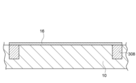
次に、表面をCMP法(Chemical Mechanical Polishing)により平坦化し、トレンチ形成のためのマスクとして形成したシリコン酸化膜12、シリコン窒化膜14を例えばドライエッチングによって除去する。これにより、シリコン基板10に形成したトレンチ15内にシリコン酸化膜が埋め込まれた素子分離膜308が形成される。
さらに、前酸化を行い、シリコン基板10上及び素子分離膜308上にシリコン酸化膜(前酸化膜)16を形成する(図4)。
(Formation of element isolation film)
Next, a silicon oxide film (buried oxide film) embedded in the
Next, the surface is flattened by CMP (Chemical Mechanical Polishing), and the silicon oxide film 12 and
Further, pre-oxidation is performed to form a silicon oxide film (pre-oxidation film) 16 on the
(ウェルの形成)
次に、イオン注入法によりシリコン基板10内の所定の深さに、例えばボロンを注入してp型の導電型を有するpウェル306を形成する。さらにシリコン基板10の表層部にヒ素またはリンを注入する。これにより、Vt(閾値)調整のためのp型の導電型を有するpウェル302を形成する(図5)。
(Formation of wells)
Next, a p-well 306 having p-type conductivity is formed by implanting boron, for example, into the
(第1ゲート絶縁膜の形成)
次に、前酸化膜16を除去した後、トランジスタ形成領域に第1ゲート絶縁膜(第1絶縁膜)102を形成する(図6)。
第1ゲート絶縁膜としては、酸化膜又は酸窒化膜が好ましい。本実施形態においては第1ゲート絶縁膜102として、例えばCVD法又は熱酸化によって、pウェル302及び素子分離膜308の表面を一体的に覆うシリコン酸化膜102を形成する。
本実施形態では、データ書き込み用電界効果トランジスタ100を形成する領域Wにおいては第1ゲート絶縁膜102と後述する第2ゲート絶縁膜104とが積層されることでデータ書き込み用電界効果トランジスタ100のゲート絶縁膜を構成することになる。一方、データ読み出し用電界効果トランジスタ200を形成する領域Rにおいては第1ゲート絶縁膜102は除去され、第2ゲート絶縁膜104がデータ読み出し用電界効果トランジスタ200を形成する領域Rのゲート絶縁膜を構成することになる。
(Formation of first gate insulating film)
Next, after removing the
An oxide film or an oxynitride film is preferable as the first gate insulating film. In this embodiment, as the first
In the present embodiment, a first
本実施形態におけるデータ書き込み用電界効果トランジスタ100のゲート絶縁膜102,104の厚みは、リテンション特性を満たす観点から4nm~10nmが好ましく、データ読み出し用電界効果トランジスタ200のゲート絶縁膜204の厚みは低電圧化の観点から2nm~4nmが好ましい。また、第1ゲート絶縁膜102は、データ書き込み用電界効果トランジスタ100に要求されるゲート絶縁膜の厚みから第2ゲート絶縁膜104,204の厚みを差し引いた厚みで形成することが好ましい。データ書き込み用電界効果トランジスタ100のゲート絶縁膜102,104の厚みは、データ読み出し用電界効果トランジスタ200のゲート絶縁膜204の厚みの2倍以上とすることが好ましいため、第1ゲート絶縁膜102は、第2ゲート絶縁膜104,204よりも大きい厚みで形成することが好ましく、具体的には、2nm~6nmの厚みで形成することが好ましい。
The thickness of the
(第1ゲート絶縁膜の一部除去)
第1ゲート絶縁膜102を形成した領域のうち、データ書き込み用電界効果トランジスタ100を形成する領域W及びデータ読み出し用電界効果トランジスタ200を形成する領域Rの一方の領域における第1ゲート絶縁膜102を除去する。本実施形態では、データ読み出し用電界効果トランジスタ200を形成する領域Rにおける第1ゲート絶縁膜102を除去する。
第1ゲート絶縁膜102のうち、データ書き込み用の電界効果トランジスタを形成する領域のみフォトリソグラフィによってレジストマスク18で覆う。そして、データ読み出し用の電界効果トランジスタを形成する領域Rにおけるレジストマスク18で覆われていない第1ゲート絶縁膜102をドライエッチング又はウエットエッチングにより除去する(図7)。
(Partial removal of the first gate insulating film)
Of the regions where the first
Only a region of the first
(第2ゲート絶縁膜形成工程)
次に、レジストマスク18を除去し、データ書き込み用電界効果トランジスタ100を形成する領域W及びデータ読み出し用電界効果トランジスタ200を形成する領域Rに第2ゲート絶縁膜(第2絶縁膜)104,204を形成する(図8)。
前述したように、本実施形態では、データ書き込み用電界効果トランジスタ100を形成する領域Wにおいては第1ゲート絶縁膜102と第2ゲート絶縁膜104とが一体となってデータ書き込み用電界効果トランジスタ100のゲート絶縁膜を構成し、データ読み出し用電界効果トランジスタ200を形成する領域Rにおいては、第2ゲート絶縁膜204がデータ読み出し用電界効果トランジスタ200のゲート絶縁膜を構成することになる。
(Second Gate Insulating Film Forming Step)
Next, the resist
As described above, in the present embodiment, in the region W where the data write
第1ゲート絶縁膜102を2nm~6nmの厚みで形成した場合、データ書き込み用電界効果トランジスタ100のリテンション特性と、データ読み出し用電界効果トランジスタ200の低電圧化の観点から、第2ゲート絶縁膜204は2nm~4nmの厚みで形成することが好ましい。これにより、データ書き込み用電界効果トランジスタ100のゲート絶縁膜は、第1ゲート絶縁膜102と第2ゲート絶縁膜104とが積層された4nm~10nmの厚みを有し、データ読み出し用電界効果トランジスタ200のゲート絶縁膜は、第2ゲート絶縁膜204による2nm~4nmの厚みを有することになる。
なお、第2ゲート絶縁膜104,204は、第1ゲート絶縁膜102と同様、酸化膜又は酸窒化膜が好ましく、例えばCVD法又は熱酸化によって形成することができる。なお、例えば、第1ゲート絶縁膜102として酸化膜を形成し、第2ゲート絶縁膜として酸化物より誘電率の高い酸窒化膜を形成してもよい。
When the first
The second
(浮遊ゲートの形成)
次に、データ書き込み用電界効果トランジスタ100を形成する領域W及びデータ読み出し用電界効果トランジスタ200を形成する領域Rのそれぞれの第2ゲート絶縁膜104,204上に浮遊ゲート106,206を形成する。
例えば、CVD法により第2ゲート絶縁膜104,204の表面にポリシリコン膜を形成する。続いて、イオン注入法により、ポリシリコン膜の全面にリンまたはヒ素を注入する。これにより、ポリシリコン膜の全体にn型の導電性が付与される。
(Formation of floating gate)
Next, floating
For example, a polysilicon film is formed on the surfaces of the second
次に、フォトリソグラフィ及びエッチングを用いて、ポリシリコン膜をパターニングする。これにより、データ書き込み用電界効果トランジスタ100の浮遊ゲート(フローティングゲート)106及びデータ読み出し用電界効果トランジスタ200の浮遊ゲート(フローティングゲート)206が形成される(図9)。
The polysilicon film is then patterned using photolithography and etching. Thereby, the floating gate (floating gate) 106 of the data write
(サイドウォールの形成)
次に、CVD法により、データ書き込み用電界効果トランジスタ100の浮遊ゲート106及びデータ読み出し用電界効果トランジスタ200の浮遊ゲート206の上面及び側面を覆うように、SiN膜を形成後、SiO2等の絶縁膜をシリコン基板10上に形成する。
続いて、上記の絶縁膜をエッチバックする。これにより、データ書き込み用電界効果トランジスタ100の浮遊ゲート106の側面を覆うサイドウォール112及びデータ読み出し用電界効果トランジスタ200の浮遊ゲート206の側面を覆うサイドウォール212が形成される(図10)。
(Sidewall formation)
Next, a SiN film is formed by the CVD method so as to cover the upper and side surfaces of the floating
Subsequently, the insulating film is etched back. As a result, a
(拡散層の形成)
次に、データ書き込み用電界効果トランジスタ100を形成する領域W及びデータ読み出し用電界効果トランジスタ200を形成する領域Rのそれぞれにおいて、シリコン基板10内のシリコン基板10の厚さ方向から見て浮遊ゲート106,206を間に挟む位置においてそれぞれソース領域及びドレイン領域を構成する拡散層310A,301B,310Cを形成する。
例えば、データ書き込み用電界効果トランジスタ100を形成する領域W及びデータ読み出し用電界効果トランジスタ200を形成する領域Rのそれぞれにおいて、シリコン基板10内のシリコン基板10の厚さ方向から見て浮遊ゲート106,206を間に挟む位置におけるpウェル302の表面にイオン注入法によりヒ素またはリンを注入する。これにより、pウェル302の表層部の、各浮遊ゲート106,206を間に挟む位置にソース・ドレインを構成するn型拡散層310A,310B,310Cがそれぞれ形成される(図11)。
(Formation of diffusion layer)
Next, in each of the region W forming the data write
For example, in each of the region W forming the data write
(酸化膜の除去/Coシリサイド層の形成)
次に、データ書き込み用電界効果トランジスタ100を形成する領域W及びデータ読み出し用電界効果トランジスタ200を形成する領域Rにおいて露出する酸化膜(ゲート絶縁膜102,104,204)を除去し、サリサイドプロセスを用いて、データ書き込み用電界効果トランジスタ100及びデータ読み出し用電界効果トランジスタ200のn型拡散層310A,310B,310Cの表面及び浮遊ゲート106,206の表面に合金層312A,312B,312C,108,208を形成する(図12)。
(Removal of oxide film/formation of Co silicide layer)
Next, the oxide films (
例えば、スパッタ法によりデータ書き込み用電界効果トランジスタ100及びデータ読み出し用電界効果トランジスタ200の表面全体を覆うように、シリコン基板10上にコバルト膜を形成する。
続いて、熱処理によってシリコンとコバルト膜とが接している部分、すなわち、n型拡散層310A,310B,310Cの表面及び浮遊ゲート106,206の表面に主としてコバルトモノシリサイド(CoSi)を含むCoシリサイド層を形成する。
続いて、薬液処理によって、データ書き込み用電界効果トランジスタ100及びデータ読み出し用電界効果トランジスタ200以外の領域(素子分離領域)におけるコバルト膜を除去する。
続いて、更なる熱処理によってコバルトモノシリサイド(CoSi)をコバルトダイシリサイド(CoSi2)に相転移させる。
これにより、n型拡散層310A,310B,310C及び浮遊ゲート106,206の表面にそれぞれ、主としてコバルトダイシリサイド(CoSi2)を含む合金層312A,312B,312C,108,208が形成される。なお、各熱処理は、加熱時間が短時間であるRTA(Rapid Thermal Anneal)によって行われる。
For example, a cobalt film is formed on the
Subsequently, a Co silicide layer mainly containing cobalt monosilicide (CoSi) is formed on the portions where the silicon and the cobalt film are in contact by heat treatment, that is, the surfaces of the n-type diffusion layers 310A, 310B, 310C and the surfaces of the floating
Subsequently, the cobalt film in the region (element isolation region) other than the data write
Cobalt monosilicide (CoSi) is then phase-transformed to cobalt disilicide (CoSi 2 ) by further heat treatment.
Thereby, alloy layers 312A, 312B, 312C, 108 and 208 mainly containing cobalt disilicide (CoSi 2 ) are formed on the surfaces of the n-type diffusion layers 310A, 310B and 310C and the floating
(層間絶縁膜の形成/コンタクトの形成)
その後、データ書き込み用電界効果トランジスタ100及びデータ読み出し用電界効果トランジスタ200を覆う層間絶縁膜(中間層)320を形成する。
さらに、データ書き込み用電界効果トランジスタ100またはデータ読み出し用電界効果トランジスタ200に接続されるコンタクト322を層間絶縁膜320内に形成する。コンタクト322を介してデータ書き込み用電界効果トランジスタ100またはデータ読み出し用電界効果トランジスタ200に接続される配線を層間絶縁膜320上に形成する工程などを経て不揮発性メモリセルが完成する(図13)。
(Formation of interlayer insulating film/formation of contact)
After that, an interlayer insulating film (intermediate layer) 320 covering the data write
Further, a
このようなプロセス工程を経ることで、例えば、データ書き込み用の電界効果トランジスタ100のゲート絶縁膜102,104をリテンション特性を満たす4nm~10nmで形成し、かつデータ読み出し用の電界効果トランジスタ200のゲート絶縁膜204は2nm~4nmと薄膜化が可能となる。このような構造を有する不揮発性メモリセルを形成することで、データ書き込み用の電界効果トランジスタのリテンション特性を損なうことなく、データ読み出し用の電界効果トランジスタのゲート電圧低電圧化が可能となる。
Through such process steps, for example, the
以上、本開示に係る半導体装置及びその製造方法について説明したが、本開示に係る半導体装置及びその製造方法は上記説明に限定されない。
例えば、本開示における不揮発性メモリの構成は図1、図2、図13に示す構成に限定されず、データ書き込み用電界効果トランジスタ及びデータ読み出し用電界効果トランジスタを有する不揮発性メモリセルを備えた半導体装置であれば、本開示を適用することができる。
また、上記実施形態では、データ書き込み用電界効果トランジスタのゲート絶縁膜の厚みが、データ読み出し用電界効果トランジスタのゲート絶縁膜の厚みよりも大きくする場合について説明したが、データ読み出し用電界効果トランジスタに高電圧の印加が要求される場合などは、データ書き込み用電界効果トランジスタのゲート絶縁膜の厚みよりも、データ読み出し用電界効果トランジスタのゲート絶縁膜の厚みを大きくしてもよい。すなわち、各電界効果トランジスタに要求される特性(特に閾値電圧)に応じてゲート絶縁膜の厚みに設定すればよい。
また、本開示に係る半導体装置の用途は限定されず、データの書き換えが要求される導体装置であれば制限でなく適用することができる。
Although the semiconductor device and the manufacturing method thereof according to the present disclosure have been described above, the semiconductor device and the manufacturing method thereof according to the present disclosure are not limited to the above description.
For example, the configuration of the nonvolatile memory in the present disclosure is not limited to the configurations shown in FIGS. The present disclosure can be applied to any device.
Further, in the above embodiment, the case where the thickness of the gate insulating film of the field effect transistor for data writing is made larger than the thickness of the gate insulating film of the field effect transistor for reading data has been described. In cases such as when application of a high voltage is required, the thickness of the gate insulating film of the data reading field effect transistor may be made larger than the thickness of the gate insulating film of the data writing field effect transistor. That is, the thickness of the gate insulating film may be set according to the characteristics (especially threshold voltage) required for each field effect transistor.
Further, the application of the semiconductor device according to the present disclosure is not limited, and any semiconductor device that requires rewriting of data can be applied without limitation.
10 シリコン基板
12 シリコン酸化膜
14 シリコン窒化膜
15 トレンチ
16 前酸化膜
18 レジストマスク
50 不揮発性メモリセル
100 データ書き込み用電界効果トランジスタ
102 第1ゲート絶縁膜(第1絶縁膜)
104 第2ゲート絶縁膜(第2絶縁膜)
106 浮遊ゲート
108 合金層
110 シリコン窒化膜
112 サイドウォール
120 シリコン窒化膜
200 データ読み出し用電界効果トランジスタ
204 第2ゲート絶縁膜(第2絶縁膜)
206 浮遊ゲート
212 サイドウォール
208 合金層
212 絶縁膜
220 シリコン窒化膜
302 pウェル
306 pウェル
308 素子分離膜
310A,310B,310C 拡散層
312A,312B,312C 合金層
320 層間絶縁膜
322 コンタクト
10 silicon substrate 12
104 second gate insulating film (second insulating film)
106 floating
206 floating
Claims (6)
前記半導体基板上に配置された不揮発性メモリセルと、を備え、
前記不揮発性メモリセルは、データ書き込み用電界効果トランジスタ、及び前記データ書き込み用電界効果トランジスタに隣接するデータ読み出し用電界効果トランジスタを含み、
前記データ書き込み用電界効果トランジスタ及び前記データ読み出し用電界効果トランジスタは、それぞれ、前記半導体基板上に形成されたゲート絶縁膜と、前記ゲート絶縁膜上に形成された浮遊ゲートと、前記半導体基板の厚さ方向から見て前記浮遊ゲートを間に挟む位置においてソース領域及びドレイン領域を構成する拡散層と、を有し、
前記拡散層は、前記データ書き込み用電界効果トランジスタ及び前記データ読み出し用電界効果トランジスタに共有されており、
前記データ読み出し用電界効果トランジスタの前記ゲート絶縁膜の厚みが、前記データ書き込み用電界効果トランジスタの前記ゲート絶縁膜の厚みよりも小さい、半導体装置。 a semiconductor substrate;
a non-volatile memory cell arranged on the semiconductor substrate;
the nonvolatile memory cell includes a data write field effect transistor and a data read field effect transistor adjacent to the data write field effect transistor;
The data write field effect transistor and the data read field effect transistor are each formed of a gate insulating film formed on the semiconductor substrate, a floating gate formed on the gate insulating film, and a thickness of the semiconductor substrate. a diffusion layer forming a source region and a drain region at a position sandwiching the floating gate when viewed from the vertical direction;
the diffusion layer is shared by the data write field effect transistor and the data read field effect transistor,
The semiconductor device according to claim 1, wherein the gate insulating film of the data read field effect transistor has a smaller thickness than the gate insulating film of the data write field effect transistor.
半導体基板の前記データ書き込み用電界効果トランジスタ及び前記データ読み出し用電界効果トランジスタを形成する領域に、前記データ書き込み用電界効果トランジスタにおけるゲート絶縁膜の厚さ方向の一部を構成するための第1絶縁膜を形成する第1絶縁膜形成工程と、
前記第1絶縁膜のうち、前記データ読み出し用電界効果トランジスタを形成する領域における前記第1絶縁膜を除去する第1絶縁膜一部除去工程と、
前記データ書き込み用電界効果トランジスタ及び前記データ読み出し用電界効果トランジスタを形成する領域に、前記第1絶縁膜とともに前記データ書き込み用電界効果トランジスタにおける前記ゲート絶縁膜を構成し、かつ、前記データ読み出し用電界効果トランジスタにおけるゲート絶縁膜を構成する第2絶縁膜を形成する第2絶縁膜形成工程と、
前記データ書き込み用電界効果トランジスタの前記ゲート絶縁膜上及び前記データ読み出し用電界効果トランジスタの前記ゲート絶縁膜上のそれぞれに浮遊ゲートを形成する工程と、
前記半導体基板の厚さ方向から見て、前記データ書き込み用電界効果トランジスタの前記浮遊ゲートを間に挟む位置においてソース領域及びドレイン領域を構成し、かつ、前記データ読み出し用電界効果トランジスタの前記浮遊ゲートを間に挟む位置においてソース領域及びドレイン領域を構成し、前記データ書き込み用電界効果トランジスタ及び前記データ読み出し用電界効果トランジスタに共有される拡散層を形成する工程と、
を含む、半導体装置の製造方法。 A method of manufacturing a semiconductor device comprising a nonvolatile memory cell including a data write field effect transistor and a data read field effect transistor adjacent to the data write field effect transistor, the method comprising:
a first insulation for forming a part of a gate insulating film in the data writing field effect transistor in a thickness direction in a region of a semiconductor substrate where the data writing field effect transistor and the data reading field effect transistor are formed; a first insulating film forming step of forming a film;
a first insulating film partial removal step of removing a portion of the first insulating film in a region where the data readout field effect transistor is to be formed;
forming the gate insulating film of the data writing field effect transistor together with the first insulating film in a region where the data writing field effect transistor and the data reading field effect transistor are formed; a second insulating film forming step of forming a second insulating film constituting a gate insulating film in an effect transistor ;
forming floating gates on the gate insulating film of the data write field effect transistor and on the gate insulating film of the data read field effect transistor;
When viewed from the thickness direction of the semiconductor substrate, a source region and a drain region are formed at positions sandwiching the floating gate of the data write field effect transistor , and the floating gate of the data read field effect transistor is provided. forming a diffusion layer that forms a source region and a drain region at a position sandwiching the data write field effect transistor and the data read field effect transistor;
A method of manufacturing a semiconductor device, comprising:
6. The method of manufacturing a semiconductor device according to claim 4 , wherein an oxide film or an oxynitride film is formed as said first insulating film and said second insulating film.
Priority Applications (3)
| Application Number | Priority Date | Filing Date | Title |
|---|---|---|---|
| JP2019069319A JP7303006B2 (en) | 2019-03-29 | 2019-03-29 | Semiconductor device and method for manufacturing semiconductor device |
| US16/802,612 US11031408B2 (en) | 2019-03-29 | 2020-02-27 | Semiconductor device and method of producing semiconductor device |
| CN202010201050.1A CN111755448A (en) | 2019-03-29 | 2020-03-20 | Semiconductor device and method of manufacturing the same |
Applications Claiming Priority (1)
| Application Number | Priority Date | Filing Date | Title |
|---|---|---|---|
| JP2019069319A JP7303006B2 (en) | 2019-03-29 | 2019-03-29 | Semiconductor device and method for manufacturing semiconductor device |
Publications (2)
| Publication Number | Publication Date |
|---|---|
| JP2020167356A JP2020167356A (en) | 2020-10-08 |
| JP7303006B2 true JP7303006B2 (en) | 2023-07-04 |
Family
ID=72604798
Family Applications (1)
| Application Number | Title | Priority Date | Filing Date |
|---|---|---|---|
| JP2019069319A Active JP7303006B2 (en) | 2019-03-29 | 2019-03-29 | Semiconductor device and method for manufacturing semiconductor device |
Country Status (3)
| Country | Link |
|---|---|
| US (1) | US11031408B2 (en) |
| JP (1) | JP7303006B2 (en) |
| CN (1) | CN111755448A (en) |
Families Citing this family (1)
| Publication number | Priority date | Publication date | Assignee | Title |
|---|---|---|---|---|
| US11610907B2 (en) * | 2021-05-27 | 2023-03-21 | Taiwan Semiconductor Manufacturing Company, Ltd. | Memory device and manufacturing method thereof |
Citations (5)
| Publication number | Priority date | Publication date | Assignee | Title |
|---|---|---|---|---|
| JP2002094029A (en) | 2000-09-14 | 2002-03-29 | Hitachi Ltd | Semiconductor device and transistor |
| JP2005026696A (en) | 2003-07-01 | 2005-01-27 | Samsung Electronics Co Ltd | EEPROM device and manufacturing method thereof |
| JP2005175411A (en) | 2003-12-12 | 2005-06-30 | Genusion:Kk | Semiconductor device and its manufacturing method |
| JP2007110073A (en) | 2005-09-13 | 2007-04-26 | Renesas Technology Corp | Semiconductor device |
| JP2016136622A (en) | 2015-01-16 | 2016-07-28 | 株式会社半導体エネルギー研究所 | Storage device and electronic apparatus |
Family Cites Families (10)
| Publication number | Priority date | Publication date | Assignee | Title |
|---|---|---|---|---|
| JPH03206661A (en) * | 1990-01-09 | 1991-09-10 | Fujitsu Ltd | Semiconductor device |
| JP3993438B2 (en) * | 2002-01-25 | 2007-10-17 | 株式会社ルネサステクノロジ | Semiconductor device |
| JP4647175B2 (en) * | 2002-04-18 | 2011-03-09 | ルネサスエレクトロニクス株式会社 | Semiconductor integrated circuit device |
| JP2004265944A (en) * | 2003-02-21 | 2004-09-24 | Handotai Rikougaku Kenkyu Center:Kk | Semiconductor storage device |
| JP2005005516A (en) * | 2003-06-12 | 2005-01-06 | Renesas Technology Corp | Semiconductor device and method of manufacturing same |
| JP4927321B2 (en) * | 2004-06-22 | 2012-05-09 | ルネサスエレクトロニクス株式会社 | Semiconductor memory device |
| JP2006196758A (en) | 2005-01-14 | 2006-07-27 | Renesas Technology Corp | Semiconductor device |
| JP2007081335A (en) * | 2005-09-16 | 2007-03-29 | Renesas Technology Corp | Semiconductor device |
| US8581260B2 (en) * | 2007-02-22 | 2013-11-12 | Semiconductor Energy Laboratory Co., Ltd. | Semiconductor device including a memory |
| JP4782070B2 (en) * | 2007-05-09 | 2011-09-28 | ルネサスエレクトロニクス株式会社 | Semiconductor integrated circuit device and manufacturing method thereof |
-
2019
- 2019-03-29 JP JP2019069319A patent/JP7303006B2/en active Active
-
2020
- 2020-02-27 US US16/802,612 patent/US11031408B2/en active Active
- 2020-03-20 CN CN202010201050.1A patent/CN111755448A/en active Pending
Patent Citations (5)
| Publication number | Priority date | Publication date | Assignee | Title |
|---|---|---|---|---|
| JP2002094029A (en) | 2000-09-14 | 2002-03-29 | Hitachi Ltd | Semiconductor device and transistor |
| JP2005026696A (en) | 2003-07-01 | 2005-01-27 | Samsung Electronics Co Ltd | EEPROM device and manufacturing method thereof |
| JP2005175411A (en) | 2003-12-12 | 2005-06-30 | Genusion:Kk | Semiconductor device and its manufacturing method |
| JP2007110073A (en) | 2005-09-13 | 2007-04-26 | Renesas Technology Corp | Semiconductor device |
| JP2016136622A (en) | 2015-01-16 | 2016-07-28 | 株式会社半導体エネルギー研究所 | Storage device and electronic apparatus |
Also Published As
| Publication number | Publication date |
|---|---|
| US11031408B2 (en) | 2021-06-08 |
| JP2020167356A (en) | 2020-10-08 |
| US20200312860A1 (en) | 2020-10-01 |
| CN111755448A (en) | 2020-10-09 |
Similar Documents
| Publication | Publication Date | Title |
|---|---|---|
| CN101996950B (en) | Semiconductor device and method of fabricating the same | |
| JP4927550B2 (en) | Nonvolatile memory device, method of manufacturing nonvolatile memory device, and nonvolatile memory array | |
| JP3908696B2 (en) | Integrated memory circuit and method of manufacturing integrated memory circuit | |
| KR100723993B1 (en) | Semiconductor memory device and manufacturing method thereof | |
| JP3726760B2 (en) | Manufacturing method of semiconductor device | |
| JP2010067645A (en) | Semiconductor device and method of manufacturing the same | |
| US9905429B2 (en) | Semiconductor device and a manufacturing method thereof | |
| US6737322B2 (en) | Method for manufacturing semiconductor device | |
| JP5142476B2 (en) | Manufacturing method of semiconductor device | |
| US20070238237A1 (en) | Structure and method for a sidewall SONOS non-volatile memory device | |
| US8952536B2 (en) | Semiconductor device and method of fabrication | |
| JP2000307086A (en) | Semiconductor device and manufacture thereof | |
| CN1979866B (en) | Storage device | |
| JP2009231300A (en) | Semiconductor memory and fabrication method therefor | |
| US20100012999A1 (en) | Semiconductor memory device and method of manufacturing the same | |
| JP7303006B2 (en) | Semiconductor device and method for manufacturing semiconductor device | |
| KR101498170B1 (en) | Semiconductor memory device and method of fabricating the same | |
| JP2011066052A (en) | Semiconductor device manufacturing method, and the semiconductor device | |
| JP3622741B2 (en) | Manufacturing method of semiconductor device | |
| US7132728B2 (en) | Non-volatile memory devices including fuse covered field regions | |
| US6916701B2 (en) | Method for fabricating a silicide layer of flat cell memory | |
| JP5123536B2 (en) | Manufacturing method of semiconductor device | |
| JP2014187132A (en) | Semiconductor device | |
| CN113471206A (en) | Multi-time programmable memory structure and manufacturing method thereof | |
| JP7007013B2 (en) | Semiconductor devices and methods for manufacturing semiconductor devices |
Legal Events
| Date | Code | Title | Description |
|---|---|---|---|
| A621 | Written request for application examination |
Free format text: JAPANESE INTERMEDIATE CODE: A621 Effective date: 20220125 |
|
| A977 | Report on retrieval |
Free format text: JAPANESE INTERMEDIATE CODE: A971007 Effective date: 20221027 |
|
| A131 | Notification of reasons for refusal |
Free format text: JAPANESE INTERMEDIATE CODE: A131 Effective date: 20221129 |
|
| A521 | Request for written amendment filed |
Free format text: JAPANESE INTERMEDIATE CODE: A523 Effective date: 20230130 |
|
| TRDD | Decision of grant or rejection written | ||
| A01 | Written decision to grant a patent or to grant a registration (utility model) |
Free format text: JAPANESE INTERMEDIATE CODE: A01 Effective date: 20230523 |
|
| A61 | First payment of annual fees (during grant procedure) |
Free format text: JAPANESE INTERMEDIATE CODE: A61 Effective date: 20230622 |
|
| R150 | Certificate of patent or registration of utility model |
Ref document number: 7303006 Country of ref document: JP Free format text: JAPANESE INTERMEDIATE CODE: R150 |