JP7084113B2 - Graphene compound, power storage device, and method for producing graphene compound - Google Patents
Graphene compound, power storage device, and method for producing graphene compound Download PDFInfo
- Publication number
- JP7084113B2 JP7084113B2 JP2017134414A JP2017134414A JP7084113B2 JP 7084113 B2 JP7084113 B2 JP 7084113B2 JP 2017134414 A JP2017134414 A JP 2017134414A JP 2017134414 A JP2017134414 A JP 2017134414A JP 7084113 B2 JP7084113 B2 JP 7084113B2
- Authority
- JP
- Japan
- Prior art keywords
- graphene
- compound
- storage device
- power storage
- graphene compound
- Prior art date
- Legal status (The legal status is an assumption and is not a legal conclusion. Google has not performed a legal analysis and makes no representation as to the accuracy of the status listed.)
- Active
Links
Images


Classifications
-
- C—CHEMISTRY; METALLURGY
- C01—INORGANIC CHEMISTRY
- C01B—NON-METALLIC ELEMENTS; COMPOUNDS THEREOF; METALLOIDS OR COMPOUNDS THEREOF NOT COVERED BY SUBCLASS C01C
- C01B32/00—Carbon; Compounds thereof
- C01B32/15—Nano-sized carbon materials
- C01B32/182—Graphene
- C01B32/194—After-treatment
-
- H—ELECTRICITY
- H01—ELECTRIC ELEMENTS
- H01M—PROCESSES OR MEANS, e.g. BATTERIES, FOR THE DIRECT CONVERSION OF CHEMICAL ENERGY INTO ELECTRICAL ENERGY
- H01M4/00—Electrodes
- H01M4/02—Electrodes composed of, or comprising, active material
- H01M4/13—Electrodes for accumulators with non-aqueous electrolyte, e.g. for lithium-accumulators; Processes of manufacture thereof
- H01M4/139—Processes of manufacture
- H01M4/1393—Processes of manufacture of electrodes based on carbonaceous material, e.g. graphite-intercalation compounds or CFx
-
- H—ELECTRICITY
- H01—ELECTRIC ELEMENTS
- H01M—PROCESSES OR MEANS, e.g. BATTERIES, FOR THE DIRECT CONVERSION OF CHEMICAL ENERGY INTO ELECTRICAL ENERGY
- H01M10/00—Secondary cells; Manufacture thereof
- H01M10/05—Accumulators with non-aqueous electrolyte
- H01M10/052—Li-accumulators
-
- H—ELECTRICITY
- H01—ELECTRIC ELEMENTS
- H01M—PROCESSES OR MEANS, e.g. BATTERIES, FOR THE DIRECT CONVERSION OF CHEMICAL ENERGY INTO ELECTRICAL ENERGY
- H01M10/00—Secondary cells; Manufacture thereof
- H01M10/05—Accumulators with non-aqueous electrolyte
- H01M10/056—Accumulators with non-aqueous electrolyte characterised by the materials used as electrolytes, e.g. mixed inorganic/organic electrolytes
- H01M10/0561—Accumulators with non-aqueous electrolyte characterised by the materials used as electrolytes, e.g. mixed inorganic/organic electrolytes the electrolyte being constituted of inorganic materials only
- H01M10/0562—Solid materials
-
- H—ELECTRICITY
- H01—ELECTRIC ELEMENTS
- H01M—PROCESSES OR MEANS, e.g. BATTERIES, FOR THE DIRECT CONVERSION OF CHEMICAL ENERGY INTO ELECTRICAL ENERGY
- H01M4/00—Electrodes
- H01M4/02—Electrodes composed of, or comprising, active material
- H01M4/04—Processes of manufacture in general
- H01M4/0471—Processes of manufacture in general involving thermal treatment, e.g. firing, sintering, backing particulate active material, thermal decomposition, pyrolysis
-
- H—ELECTRICITY
- H01—ELECTRIC ELEMENTS
- H01M—PROCESSES OR MEANS, e.g. BATTERIES, FOR THE DIRECT CONVERSION OF CHEMICAL ENERGY INTO ELECTRICAL ENERGY
- H01M4/00—Electrodes
- H01M4/02—Electrodes composed of, or comprising, active material
- H01M4/13—Electrodes for accumulators with non-aqueous electrolyte, e.g. for lithium-accumulators; Processes of manufacture thereof
- H01M4/139—Processes of manufacture
- H01M4/1395—Processes of manufacture of electrodes based on metals, Si or alloys
-
- H—ELECTRICITY
- H01—ELECTRIC ELEMENTS
- H01M—PROCESSES OR MEANS, e.g. BATTERIES, FOR THE DIRECT CONVERSION OF CHEMICAL ENERGY INTO ELECTRICAL ENERGY
- H01M4/00—Electrodes
- H01M4/02—Electrodes composed of, or comprising, active material
- H01M4/36—Selection of substances as active materials, active masses, active liquids
- H01M4/60—Selection of substances as active materials, active masses, active liquids of organic compounds
-
- H—ELECTRICITY
- H01—ELECTRIC ELEMENTS
- H01M—PROCESSES OR MEANS, e.g. BATTERIES, FOR THE DIRECT CONVERSION OF CHEMICAL ENERGY INTO ELECTRICAL ENERGY
- H01M4/00—Electrodes
- H01M4/02—Electrodes composed of, or comprising, active material
- H01M4/62—Selection of inactive substances as ingredients for active masses, e.g. binders, fillers
- H01M4/621—Binders
- H01M4/622—Binders being polymers
-
- H—ELECTRICITY
- H01—ELECTRIC ELEMENTS
- H01M—PROCESSES OR MEANS, e.g. BATTERIES, FOR THE DIRECT CONVERSION OF CHEMICAL ENERGY INTO ELECTRICAL ENERGY
- H01M10/00—Secondary cells; Manufacture thereof
- H01M10/05—Accumulators with non-aqueous electrolyte
- H01M10/054—Accumulators with insertion or intercalation of metals other than lithium, e.g. with magnesium or aluminium
-
- H—ELECTRICITY
- H01—ELECTRIC ELEMENTS
- H01M—PROCESSES OR MEANS, e.g. BATTERIES, FOR THE DIRECT CONVERSION OF CHEMICAL ENERGY INTO ELECTRICAL ENERGY
- H01M4/00—Electrodes
- H01M4/02—Electrodes composed of, or comprising, active material
- H01M2004/026—Electrodes composed of, or comprising, active material characterised by the polarity
- H01M2004/027—Negative electrodes
-
- H—ELECTRICITY
- H01—ELECTRIC ELEMENTS
- H01M—PROCESSES OR MEANS, e.g. BATTERIES, FOR THE DIRECT CONVERSION OF CHEMICAL ENERGY INTO ELECTRICAL ENERGY
- H01M4/00—Electrodes
- H01M4/02—Electrodes composed of, or comprising, active material
- H01M2004/026—Electrodes composed of, or comprising, active material characterised by the polarity
- H01M2004/028—Positive electrodes
-
- H—ELECTRICITY
- H01—ELECTRIC ELEMENTS
- H01M—PROCESSES OR MEANS, e.g. BATTERIES, FOR THE DIRECT CONVERSION OF CHEMICAL ENERGY INTO ELECTRICAL ENERGY
- H01M2220/00—Batteries for particular applications
- H01M2220/30—Batteries in portable systems, e.g. mobile phone, laptop
-
- H—ELECTRICITY
- H01—ELECTRIC ELEMENTS
- H01M—PROCESSES OR MEANS, e.g. BATTERIES, FOR THE DIRECT CONVERSION OF CHEMICAL ENERGY INTO ELECTRICAL ENERGY
- H01M2300/00—Electrolytes
- H01M2300/0017—Non-aqueous electrolytes
- H01M2300/0065—Solid electrolytes
-
- H—ELECTRICITY
- H01—ELECTRIC ELEMENTS
- H01M—PROCESSES OR MEANS, e.g. BATTERIES, FOR THE DIRECT CONVERSION OF CHEMICAL ENERGY INTO ELECTRICAL ENERGY
- H01M2300/00—Electrolytes
- H01M2300/0017—Non-aqueous electrolytes
- H01M2300/0065—Solid electrolytes
- H01M2300/0068—Solid electrolytes inorganic
-
- H—ELECTRICITY
- H01—ELECTRIC ELEMENTS
- H01M—PROCESSES OR MEANS, e.g. BATTERIES, FOR THE DIRECT CONVERSION OF CHEMICAL ENERGY INTO ELECTRICAL ENERGY
- H01M50/00—Constructional details or processes of manufacture of the non-active parts of electrochemical cells other than fuel cells, e.g. hybrid cells
- H01M50/40—Separators; Membranes; Diaphragms; Spacing elements inside cells
- H01M50/409—Separators, membranes or diaphragms characterised by the material
- H01M50/449—Separators, membranes or diaphragms characterised by the material having a layered structure
-
- Y—GENERAL TAGGING OF NEW TECHNOLOGICAL DEVELOPMENTS; GENERAL TAGGING OF CROSS-SECTIONAL TECHNOLOGIES SPANNING OVER SEVERAL SECTIONS OF THE IPC; TECHNICAL SUBJECTS COVERED BY FORMER USPC CROSS-REFERENCE ART COLLECTIONS [XRACs] AND DIGESTS
- Y02—TECHNOLOGIES OR APPLICATIONS FOR MITIGATION OR ADAPTATION AGAINST CLIMATE CHANGE
- Y02E—REDUCTION OF GREENHOUSE GAS [GHG] EMISSIONS, RELATED TO ENERGY GENERATION, TRANSMISSION OR DISTRIBUTION
- Y02E60/00—Enabling technologies; Technologies with a potential or indirect contribution to GHG emissions mitigation
- Y02E60/10—Energy storage using batteries
Landscapes
- Chemical & Material Sciences (AREA)
- Engineering & Computer Science (AREA)
- Chemical Kinetics & Catalysis (AREA)
- Electrochemistry (AREA)
- General Chemical & Material Sciences (AREA)
- Manufacturing & Machinery (AREA)
- Materials Engineering (AREA)
- Organic Chemistry (AREA)
- Inorganic Chemistry (AREA)
- Condensed Matter Physics & Semiconductors (AREA)
- General Physics & Mathematics (AREA)
- Nanotechnology (AREA)
- Physics & Mathematics (AREA)
- Secondary Cells (AREA)
- Battery Electrode And Active Subsutance (AREA)
- Carbon And Carbon Compounds (AREA)
Description
本発明の一態様は、グラフェン化合物及び蓄電装置に関する。 One aspect of the present invention relates to a graphene compound and a power storage device.
なお、本発明の一態様は、上記の技術分野に限定されない。本明細書等で開示する発明の一態様の技術分野は、物、方法、又は製造方法に関するものである。または、本発明の一態様は、プロセス、マシン、マニュファクチャ、又は組成物(コンポジション・オブ・マター)に関するものである。そのため、より具体的に本明細書で開示する本発明の一態様の技術分野としては、半導体装置、表示装置、発光装置、蓄電装置、記憶装置、それらの駆動方法、又はそれらの製造方法、を一例として挙げることができる。 It should be noted that one aspect of the present invention is not limited to the above technical fields. The technical field of one aspect of the invention disclosed in the present specification and the like relates to a product, a method, or a manufacturing method. Alternatively, one aspect of the invention relates to a process, machine, manufacture, or composition (composition of matter). Therefore, more specifically, as the technical field of one aspect of the present invention disclosed in the present specification, a semiconductor device, a display device, a light emitting device, a power storage device, a storage device, a driving method thereof, or a manufacturing method thereof. It can be given as an example.
近年、リチウムイオン蓄電池等の蓄電池、リチウムイオンキャパシタ、空気電池等、種々の蓄電装置の開発が盛んに行われている。特に高出力、高エネルギー密度であるリチウムイオン蓄電池は、携帯電話やスマートフォン、ノート型パーソナルコンピュータ等の携帯情報端末、携帯音楽プレーヤ、デジタルカメラ等の電子機器、あるいは医療機器、ハイブリッド車(HEV)、電気自動車(EV)、又はプラグインハイブリッド車(PHEV)等の次世代クリーンエネルギー自動車など、半導体産業の発展に伴い急速にその需要が拡大し、充電可能なエネルギーの供給源として現代の情報化社会に不可欠なものとなっている。 In recent years, various power storage devices such as storage batteries such as lithium ion storage batteries, lithium ion capacitors, and air batteries have been actively developed. In particular, lithium-ion storage batteries with high output and high energy density include mobile information terminals such as mobile phones, smartphones, and notebook personal computers, electronic devices such as portable music players and digital cameras, medical devices, and hybrid vehicles (HEVs). With the development of the semiconductor industry, such as next-generation clean energy vehicles such as electric vehicles (EV) and plug-in hybrid vehicles (PHEV), the demand for them has expanded rapidly, and the modern computerized society has become a source of rechargeable energy. Has become indispensable to.
しかし、一般的にリチウムイオン蓄電池は、エネルギー密度が高い一方で、電解液に高温で発火する危険のある有機溶媒が用いられているため、充放電を制御する保護回路が故障するかセルに損傷が生じる又は内部ショート(内部短絡)等により、発熱、発火や爆発するおそれがある。また、しばしばそのような事故が報告されている。 However, while lithium-ion storage batteries generally have a high energy density, the electrolyte uses an organic solvent that can ignite at high temperatures, so the protection circuit that controls charging and discharging fails or the cell is damaged. There is a risk of heat generation, ignition or explosion due to internal short circuit (internal short circuit) or the like. Also, such accidents are often reported.
その危険性を低減する方法の一つとして、電解液を固体電解質に置き換えた全固体電池が研究されている。例えば、固体電解質として、リチウムイオン伝導性のあるポリマー電解質を用いた蓄電装置が研究されている。 As one of the methods for reducing the risk, an all-solid-state battery in which the electrolytic solution is replaced with a solid electrolyte is being studied. For example, as a solid electrolyte, a power storage device using a polymer electrolyte having lithium ion conductivity has been studied.
しかし、ポリマー電解質を用いたリチウムイオン蓄電池であっても、電池が低温になるとイオン伝導性が大きく低下し、電池としての特性が大きく損なわれる場合がある。例えば、リチウムイオン蓄電池に用いることができるポリマーとしてポリエチレンオキシド(PEO)が知られているが(特許文献1)、低温で使用するとイオン伝導性が低下し問題となる場合がある。また、PEOの融点は60℃付近にあり、融解すると電極間が短絡し危険な場合があるから、使用可能な温度範囲は狭い。 However, even in a lithium ion storage battery using a polymer electrolyte, when the temperature of the battery becomes low, the ionic conductivity is greatly reduced, and the characteristics of the battery may be significantly impaired. For example, polyethylene oxide (PEO) is known as a polymer that can be used in a lithium ion storage battery (Patent Document 1), but when used at a low temperature, ionic conductivity may decrease, which may cause a problem. Further, the melting point of PEO is around 60 ° C., and when it is melted, the electrodes may be short-circuited and dangerous, so that the usable temperature range is narrow.
全固体電池における固体電解質に求められる基本的な性能としては、電荷の移動を担うイオンの伝導性が高いことと、その一方で、正極と負極との間のショート(内部短絡)を防止するために電子伝導性が低いことが挙げられる。 The basic performance required of a solid electrolyte in an all-solid-state battery is to have high conductivity of ions responsible for charge transfer, and on the other hand, to prevent a short circuit (internal short circuit) between the positive electrode and the negative electrode. The low electron conductivity is mentioned.
蓄電装置は様々な環境下で広く用いられるため、実用的な全固体のリチウムイオン蓄電池を実現するためには、高温においても上述の基本的な性能を発揮することができる固体電解質が必要である。すなわち、高温環境に耐え得ることができる固体電解質が必要である。例えば、ポリエチレンオキシド(PEO)のような固体電解質としての性能を発現する機能を有しながらも、耐熱性に優れた材料が必要である。 Since the power storage device is widely used in various environments, in order to realize a practical all-solid-state lithium-ion storage battery, a solid electrolyte capable of exhibiting the above-mentioned basic performance even at high temperatures is required. .. That is, a solid electrolyte that can withstand a high temperature environment is required. For example, there is a need for a material having excellent heat resistance while having a function of exhibiting performance as a solid electrolyte such as polyethylene oxide (PEO).
また近年、変形が可能な電子機器の開発が盛んであり、そのような可撓性を有する電子機器を実現するためには、該電子機器に用いられる部材もまた変形できる必要がある。該電子機器の筐体やディスプレイ部が可撓性を有することが求められるが、該電子機器に搭載される蓄電装置も可撓性を有することが求められる。 Further, in recent years, the development of a deformable electronic device has been active, and in order to realize such a flexible electronic device, it is necessary that the member used for the electronic device can also be deformed. The housing and display portion of the electronic device are required to have flexibility, but the power storage device mounted on the electronic device is also required to have flexibility.
可撓性を有する蓄電装置を実現するためには、該蓄電装置に用いられる各部材も可撓性を有している必要があるため、固体電解質においても可撓性を有することが求められる。PEOのようなポリマー系の固体電解質以外に、セラミックスの固体電解質も広く研究が行われている。セラミックスの固体電解質はポリマー系の固体電解質よりも高いイオン伝導度を示す傾向にあるが、セラミックスの固体電解質は割れやすく、また活物質と固体電解質の接点が取りづらいため可撓性はあまり期待できない。 In order to realize a flexible power storage device, each member used in the power storage device must also have flexibility, so that the solid electrolyte is also required to have flexibility. In addition to polymer-based solid electrolytes such as PEO, ceramic solid electrolytes have also been widely studied. Ceramic solid electrolytes tend to show higher ionic conductivity than polymer-based solid electrolytes, but ceramic solid electrolytes are fragile and difficult to contact between the active material and the solid electrolyte, so flexibility cannot be expected so much. ..
上記に鑑み、本発明の一態様は、蓄電装置の固体電解質に用いることができる材料を提供することを課題の一とする。また、イオン伝導度の高い材料を提供することを課題の一とする。また、溶媒への分散性が高い材料を提供することを課題の一とする。また、広い温度範囲で使用できる材料を提供することを課題の一とする。また、形状変化に耐えられる材料を提供することを課題の一とする。また、化学修飾されたグラフェン化合物を提供することを課題の一とする。また、新規なグラフェン化合物を提供することを課題の一とする。 In view of the above, one aspect of the present invention is to provide a material that can be used as a solid electrolyte of a power storage device. Another issue is to provide a material having high ionic conductivity. Another issue is to provide a material having high dispersibility in a solvent. Another issue is to provide a material that can be used in a wide temperature range. Another issue is to provide a material that can withstand shape changes. Another object of the present invention is to provide a chemically modified graphene compound. Another issue is to provide a novel graphene compound.
また、本発明の一態様は、形状が変化できる機能を有する蓄電装置、つまり可撓性を有する蓄電装置を提供することを課題の一とする。また、新規のグラフェン化合物を用いた可撓性を有する新規な蓄電装置を提供することを課題の一とする。 Further, one aspect of the present invention is to provide a power storage device having a function of changing its shape, that is, a flexible power storage device. Another object of the present invention is to provide a new power storage device having flexibility using a new graphene compound.
なお、これらの課題の記載は、他の課題の存在を妨げるものではない。なお、本発明の一態様は、これらの課題の全てを解決する必要はないものとする。なお、これら以外の課題は、明細書、図面、請求項などの記載から、自ずと明らかとなるものであり、明細書、図面、請求項などの記載から、これら以外の課題を抽出することが可能である。 The description of these issues does not preclude the existence of other issues. It should be noted that one aspect of the present invention does not need to solve all of these problems. Issues other than these are self-evident from the description of the description, drawings, claims, etc., and it is possible to extract problems other than these from the description of the specification, drawings, claims, etc. Is.
上記に鑑み、本発明の一態様は、置換または無置換の鎖状の基及びグラフェン層を有し、鎖状の基はエステル基又はカルボキシル基を1以上有し、鎖状の基はSi原子を有し、鎖状の基がSi原子を介してグラフェン層と結合されたグラフェン化合物である。 In view of the above, one embodiment of the present invention has a substituted or unsubstituted chain group and a graphene layer, the chain group has one or more ester groups or carboxyl groups, and the chain group is a Si atom. It is a graphene compound in which a chain group is bonded to a graphene layer via a Si atom.
また、本発明の他の一態様は、置換または無置換の鎖状の基及びグラフェン層を有し、鎖状の基はエステル基又はカルボキシル基を1以上10以下有し、鎖状の基はSi原子を有し、鎖状の基がSi原子を介してグラフェン層と結合されたグラフェン化合物である。 In addition, another aspect of the present invention has a substituted or unsubstituted chain group and a graphene layer, the chain group has an ester group or a carboxyl group of 1 or more and 10 or less, and the chain group is a chain group. It is a graphene compound having a Si atom and having a chain group bonded to the graphene layer via the Si atom.
また、本発明の他の一態様は、置換または無置換の鎖状の基及びグラフェン層を有し、鎖状の基は、エステル基又はカルボキシル基を1つ有し、鎖状の基はSi原子を有し、鎖状の基がSi原子を介してグラフェン層と結合されたグラフェン化合物である。 In addition, another aspect of the present invention has a substituted or unsubstituted chain group and a graphene layer, the chain group has one ester group or a carboxyl group, and the chain group is Si. It is a graphene compound having an atom and having a chain group bonded to the graphene layer via a Si atom.
また、本発明の他の一態様は、一般式(G1)で表される構造を有するグラフェン化合物である。

(一般式(G1)において、G layerはグラフェン層を表し、R1は置換または無置換の炭素数1乃至炭素数20のアルキル基を表し、R2は水素、又は置換若しくは無置換の炭素数1乃至炭素数20のアルキル基を表す。)
Further, another aspect of the present invention is a graphene compound having a structure represented by the general formula (G1).
(In the general formula (G1), Grayer represents a graphene layer, R 1 represents a substituted or unsubstituted alkyl group having 1 to 20 carbon atoms, and R 2 represents hydrogen or a substituted or unsubstituted carbon number. Represents an alkyl group having 1 to 20 carbon atoms.)
また、本発明の他の一態様は、一般式(G1)中、R1は置換または無置換の炭素数1乃至炭素数11のアルキル基であり、R2は置換または無置換の炭素数1乃至炭素数11のアルキル基であるグラフェン化合物である。 In another aspect of the present invention, in the general formula (G1), R 1 is a substituted or unsubstituted alkyl group having 1 to 11 carbon atoms, and R 2 is a substituted or unsubstituted alkyl group having 1 carbon atom. It is a graphene compound which is an alkyl group having 11 carbon atoms.
また、本発明の他の一態様は、一般式(G2)で表される構造を有するグラフェン化合物である。

(一般式(G2)において、G layerはグラフェン層を表し、R1は置換または無置換の炭素数1乃至炭素数20のアルキル基を表し、R2は水素、又は置換若しくは無置換の炭素数1乃至炭素数20のアルキル基を表す。)
Further, another aspect of the present invention is a graphene compound having a structure represented by the general formula (G2).
(In the general formula (G2), Grayer represents a graphene layer, R 1 represents a substituted or unsubstituted alkyl group having 1 to 20 carbon atoms, and R 2 represents hydrogen or a substituted or unsubstituted carbon number. Represents an alkyl group having 1 to 20 carbon atoms.)
また、本発明の他の一態様は、一般式(G2)中、R1は置換または無置換の炭素数1乃至炭素数11のアルキル基であり、R2は置換または無置換の炭素数1乃至炭素数11のアルキル基であるグラフェン化合物である。 In another aspect of the present invention, in the general formula (G2), R 1 is a substituted or unsubstituted alkyl group having 1 to 11 carbon atoms, and R 2 is a substituted or unsubstituted alkyl group having 1 carbon atom. It is a graphene compound which is an alkyl group having 11 carbon atoms.
また、本発明の他の一態様は、構造式(202)で表される構造を有するグラフェン化合物である。

(構造式(202)中において、G layerはグラフェン層を表す。)
Further, another aspect of the present invention is a graphene compound having a structure represented by the structural formula (202).
(In structural formula (202), Grayer represents a graphene layer.)
また、本発明の他の一態様は、構造式(203)で表される構造を有するグラフェン化合物である。

(構造式(203)中において、G layerはグラフェン層を表す。)
Further, another aspect of the present invention is a graphene compound having a structure represented by the structural formula (203).
(In structural formula (203), Grayer represents a graphene layer.)
また、本発明の他の一態様は、構造式(204)で表される構造を有するグラフェン化合物である。

(構造式(204)中において、G layerはグラフェン層を表す。)
Further, another aspect of the present invention is a graphene compound having a structure represented by the structural formula (204).
(In structural formula (204), Grayer represents a graphene layer.)
また、本発明の他の一態様は、上記に記載のグラフェン化合物と、外装体と、正極集電体と、負極集電体と、を有する蓄電装置である。 Further, another aspect of the present invention is a power storage device including the graphene compound described above, an exterior body, a positive electrode current collector, and a negative electrode current collector.
また、本発明の他の一態様は、酸化グラフェンと、ルイス塩基とを、撹拌して第1の混合液を形成し、第1の混合液に、1つ以上のエステル基又はカルボキシル基を有するケイ素化合物を混合し撹拌して第2の混合液を形成し、第2の混合液をろ過し、得られたろ取物を回収し、ろ取物がグラフェン化合物を含むことを特徴とするグラフェン化合物の製造方法である。 Further, in another aspect of the present invention, graphene oxide and Lewis base are stirred to form a first mixed solution, and the first mixed solution has one or more ester groups or carboxyl groups. The graphene compound is characterized in that the silicon compound is mixed and stirred to form a second mixture, the second mixture is filtered, and the obtained filtrate is collected, and the filtrate contains a graphene compound. It is a manufacturing method of.
また、前述のグラフェン化合物の製造方法において、ルイス塩基は、ブチルアミン、ペンチルアミン、ヘキシルアミン、ジエチルアミン、ジプロピルアミン、ジブチルアミン、トリエチルアミン、トリプロピルアミン、ピリジンのいずれか一以上であることが好ましい。 Further, in the above-mentioned method for producing a graphene compound, the Lewis base is preferably any one or more of butylamine, pentylamine, hexylamine, diethylamine, dipropylamine, dibutylamine, triethylamine, tripropylamine and pyridine.
また、本発明の他の一態様は、酸化グラフェンと、ブチルアミンとを、撹拌して第1の混合液を形成し、第1の混合液に、ケイ素化合物を混合し撹拌して第2の混合液を形成し、ケイ素化合物は11-アセトキシウンデシルトリクロロシラン、2-アセトキシエチルトリクロロシランまたは2-(カルボメトキシ)エチルトリクロロシランのいずれかであり、第2の混合液をろ過し、得られたろ取物を回収し、ろ取物はグラフェン化合物を含むことを特徴とするグラフェン化合物の製造方法である。 Further, in another aspect of the present invention, graphene oxide and butylamine are stirred to form a first mixed solution, and a silicon compound is mixed with the first mixed solution and stirred to form a second mixed solution. A liquid was formed, and the silicon compound was either 11-acetoxyundecyltrichlorosilane, 2-acetoxyethyltrichlorosilane or 2- (carbomethoxy) ethyltrichlorosilane, and the second mixed liquid was filtered to obtain a filter. A method for producing a graphene compound, which comprises collecting a sample and containing the graphene compound.
本発明の一態様により、蓄電装置の固体電解質に用いることができる材料を提供できる。また、イオン伝導度の高い材料を提供できる。また、溶媒への分散性が高い材料を提供できる。また、広い温度範囲で使用できる材料を提供できる。また、形状変化に耐えられる材料を提供できる。また、化学修飾されたグラフェン化合物を提供できる。また、新規なグラフェン化合物を提供できる。 According to one aspect of the present invention, it is possible to provide a material that can be used as a solid electrolyte of a power storage device. Further, it is possible to provide a material having high ionic conductivity. Further, it is possible to provide a material having high dispersibility in a solvent. Further, it is possible to provide a material that can be used in a wide temperature range. Further, it is possible to provide a material that can withstand a change in shape. Further, a chemically modified graphene compound can be provided. In addition, a novel graphene compound can be provided.
また、本発明の一態様により、形状が変化できる機能を有する蓄電装置、つまり可撓性を有する蓄電装置を提供できる。また、新規のグラフェン化合物を用いた可撓性を有する新規な蓄電装置を提供できる。 Further, according to one aspect of the present invention, it is possible to provide a power storage device having a function of changing its shape, that is, a flexible power storage device. Further, it is possible to provide a novel power storage device having flexibility using a novel graphene compound.
なお、これらの効果の記載は、他の効果の存在を妨げるものではない。なお、本発明の一態様は、必ずしも、これらの効果の全てを有する必要はない。なお、これら以外の効果は、明細書、図面、請求項などの記載から、自ずと明らかとなるものであり、明細書、図面、請求項などの記載から、これら以外の効果を抽出することが可能である。 The description of these effects does not preclude the existence of other effects. It should be noted that one aspect of the present invention does not necessarily have to have all of these effects. It should be noted that the effects other than these are self-evident from the description of the description, drawings, claims, etc., and it is possible to extract the effects other than these from the description of the description, drawings, claims, etc. Is.
以下では、本発明の実施の形態について図面を用いて詳細に説明する。ただし、本発明は以下の説明に限定されず、その形態および詳細を様々に変更し得ることは、当業者であれば容易に理解される。また、本発明は以下に示す実施の形態の記載内容に限定して解釈されるものではない。 Hereinafter, embodiments of the present invention will be described in detail with reference to the drawings. However, the present invention is not limited to the following description, and it is easily understood by those skilled in the art that the form and details thereof can be changed in various ways. Further, the present invention is not limited to the description of the embodiments shown below.
なお、本明細書で説明する各図において、正極、負極、活物質層、セパレータ、外装体などの各構成要素の大きさや厚さ等は、個々に説明の明瞭化のために誇張されている場合がある。よって、必ずしも各構成要素はその大きさに限定されず、また各構成要素間での相対的な大きさに限定されない。 In each of the figures described in the present specification, the size and thickness of each component such as the positive electrode, the negative electrode, the active material layer, the separator, and the exterior body are individually exaggerated for the purpose of clarifying the explanation. In some cases. Therefore, each component is not necessarily limited to its size, nor is it limited to the relative size between the components.
また、本明細書等において、第1、第2、第3などとして付される序数詞は、便宜上用いるものであって工程の順番や上下の位置関係などを示すものではない。そのため、例えば、「第1の」を「第2の」又は「第3の」などと適宜置き換えて説明することができる。また、本明細書等に記載されている序数詞と、本発明の一態様を特定するために用いられる序数詞は一致しない場合がある。 Further, in the present specification and the like, the ordinal numbers attached as the first, second, third and the like are used for convenience and do not indicate the order of processes or the positional relationship between the upper and lower parts. Therefore, for example, the "first" can be appropriately replaced with the "second" or "third" for explanation. In addition, the ordinal numbers described in the present specification and the like may not match the ordinal numbers used to specify one aspect of the present invention.
また、本明細書等で説明する本発明の構成において、同一部分又は同様の機能を有する部分には同一の符号を異なる図面間で共通して用い、その繰り返しの説明は省略する。また、同様の機能を有する部分を指す場合には、ハッチパターンを同じくし、特に符号を付さない場合がある。 Further, in the configuration of the present invention described in the present specification and the like, the same reference numerals are commonly used between different drawings for the same parts or parts having similar functions, and the repeated description thereof will be omitted. Further, when referring to a portion having the same function, the hatch pattern may be the same and no particular reference numeral may be added.
また、本明細書において可撓性とは、物体が柔軟であり、曲がることが可能である性質を指す。物体にかかる外力に応じて物体が変形することができる性質であり、弾性や変形前の形状への復元性の有無を問題にはしない。可撓性を有する物体は、外力に応じて変形することができる。可撓性を有する物体は、変形した状態で固定して使用することもでき、繰り返し変形させて使用してもよく、変形していない状態で使用することもできる。 Further, as used herein, the term "flexibility" refers to the property that an object is flexible and can bend. It is a property that an object can be deformed according to an external force applied to the object, and it does not matter whether or not there is elasticity or resilience to the shape before deformation. A flexible object can be deformed in response to an external force. The flexible object can be fixed and used in a deformed state, may be repeatedly deformed and used, or can be used in a non-deformed state.
また、本明細書において化学修飾とは、グラフェン化合物を化学的に変化させ、グラフェン化合物の機能又は性質を変化させることをいう場合がある。さらに、特定の機能又は性質を有する官能基を付加することをいう場合もある。 Further, in the present specification, chemical modification may mean chemically changing a graphene compound to change the function or property of the graphene compound. Further, it may refer to adding a functional group having a specific function or property.
また、この発明を実施するための形態に記載の内容は、適宜組み合わせて用いることができる。 In addition, the contents described in the embodiment for carrying out the present invention can be used in combination as appropriate.
(実施の形態1)
本実施の形態では、本発明の一態様により製造されるグラフェン化合物について説明する。また、化学修飾によるグラフェン化合物の製造方法についても合わせて説明する。本発明の一態様により製造されたグラフェン化合物は、リチウム、ナトリウム、マグネシウム、カルシウム等の金属イオンを伝導する機能を有し、例えば、リチウムイオン蓄電池の固体電解質に用いることができる。ただし、本発明の一態様はこれに限定されない。
(Embodiment 1)
In this embodiment, the graphene compound produced by one aspect of the present invention will be described. In addition, a method for producing a graphene compound by chemical modification will also be described. The graphene compound produced according to one aspect of the present invention has a function of conducting metal ions such as lithium, sodium, magnesium and calcium, and can be used, for example, as a solid electrolyte of a lithium ion storage battery. However, one aspect of the present invention is not limited to this.
<グラフェン化合物>
まず、グラフェンとグラフェン化合物について説明する。
<Graphene compound>
First, graphene and graphene compounds will be described.
グラフェンとは、炭素原子がsp2混成軌道で結合している1原子層のシートであり、炭素原子が平面上に六角形格子構造で配列している。ダイヤモンド以上に炭素原子間の結合が強く、変形や引っ張りに非常に大きな耐性を有している材料である。一方で、電子伝導性が極めて高く、また、リチウムイオンは十分には透過しないため、そのままではリチウムイオン蓄電池の固体電解質に用いるには不適である。 Graphene is a sheet of a single atomic layer in which carbon atoms are bonded in sp2 hybrid orbitals, and carbon atoms are arranged on a plane in a hexagonal lattice structure. It is a material that has stronger bonds between carbon atoms than diamond and has extremely high resistance to deformation and tension. On the other hand, since the electron conductivity is extremely high and lithium ions do not sufficiently permeate, it is not suitable for use as a solid electrolyte in a lithium ion storage battery as it is.
炭素原子が1原子層配列したグラフェンを、単層グラフェンと呼ぶ場合がある。グラフェンが2層以上100層以下重なったものを、マルチグラフェンと呼ぶ場合がある。単層グラフェンおよびマルチグラフェンは、例えば、長手方向、あるいは面における長軸の長さが50nm以上100μm以下、又は800nm以上50μm以下である。なお、本明細書において、グラフェンには、単層グラフェンおよびマルチグラフェンを含む。 Graphene in which one carbon atom is arranged in one atomic layer may be called single-layer graphene. A stack of two or more layers and 100 or less layers of graphene may be referred to as multi-graphene. The single-layer graphene and multi-graphene have, for example, a length of a major axis in the longitudinal direction or in a plane of 50 nm or more and 100 μm or less, or 800 nm or more and 50 μm or less. In addition, in this specification, graphene includes single-layer graphene and multi-graphene.
しかし、一般的にグラフェンは様々な種類の欠陥を有している場合がある。例えば、格子を形成する炭素が欠けていることがあり、また、格子に六員環以外に五員環や七員環が存在することがある。また、炭素又は炭素以外の元素を含む官能基を有する場合がある。そのような欠陥サイトを利用して原子や原子団をグラフェンと結合させて、所望の性質を発現させることができる。 However, in general graphene may have various types of defects. For example, the carbon that forms the lattice may be missing, and the lattice may have a five-membered ring or a seven-membered ring in addition to the six-membered ring. In addition, it may have a functional group containing carbon or an element other than carbon. Such defective sites can be utilized to bind atoms or groups of atoms to graphene to develop the desired properties.
本明細書等において、グラフェンを基本骨格として有する化合物をグラフェン化合物(GC:Graphene Compound)と呼ぶ。なお、本明細書において、単層グラフェンおよびマルチグラフェンはそれぞれグラフェン化合物に含まれる。 In the present specification and the like, a compound having graphene as a basic skeleton is referred to as a graphene compound (GC). In this specification, monolayer graphene and multigraphene are included in graphene compounds, respectively.
以下に、グラフェン化合物について詳細を説明する。 The graphene compound will be described in detail below.
グラフェン化合物は例えば、グラフェンが炭素以外の原子、又は炭素以外の原子を有する原子団に化学修飾された化合物である。また、グラフェンが、アルキル基、アルキレン基等の炭素を主とした原子団に化学修飾された化合物であってもよい。なお、グラフェンを化学修飾する原子団を、化学修飾基、修飾基、置換基、官能基、又は特性基等と呼ぶ場合がある。ここで、本明細書等において化学修飾とは、置換反応、付加反応、又はその他の反応により、グラフェン、マルチグラフェン、グラフェン化合物、又は酸化グラフェン(後述)に、原子団を導入することをいう。 The graphene compound is, for example, a compound in which graphene is chemically modified into an atom other than carbon or an atomic group having an atom other than carbon. Further, graphene may be a compound chemically modified into a carbon-based atomic group such as an alkyl group and an alkylene group. The atomic group that chemically modifies graphene may be referred to as a chemically modifying group, a modifying group, a substituent, a functional group, a characteristic group, or the like. Here, in the present specification and the like, the chemical modification means to introduce an atomic group into graphene, multigraphene, a graphene compound, or graphene oxide (described later) by a substitution reaction, an addition reaction, or another reaction.
化学修飾は、1種類の原子又は原子団を導入するだけでなく、複数の種類の化学修飾を施し、複数の種類の原子又は原子団を導入することも指す。また、化学修飾は、水素、ハロゲン原子、炭化水素基、芳香族炭化水素基、複素環化合物基を付加する反応も含まれる。また、グラフェンに原子団を導入する反応として、付加反応、置換反応等が挙げられる。また、フリーデル・クラフツ(Friedel-Crafts)反応、ビンゲル(Bingel)反応等を行ってもよい。グラフェンに対してラジカル付加反応を行ってもよく、シクロ付加反応によりグラフェンと原子団との間に環を形成してもよい。 Chemical modification refers not only to the introduction of one type of atom or atomic group, but also to the introduction of a plurality of types of chemical modifications and the introduction of a plurality of types of atoms or atomic groups. Chemical modifications also include reactions that add hydrogen, halogen atoms, hydrocarbon groups, aromatic hydrocarbon groups, and heterocyclic compound groups. In addition, examples of the reaction for introducing an atomic group into graphene include an addition reaction and a substitution reaction. Further, a Friedel-Crafts reaction, a Bingel reaction and the like may be carried out. A radical addition reaction may be carried out on graphene, or a ring may be formed between graphene and an atomic group by a cyclo addition reaction.
なお、グラフェンの表面と裏面は、それぞれ異なる原子や原子団により化学修飾されていてもよい。また、マルチグラフェンにおいては、それぞれの層が異なる原子や原子団に化学修飾されていてもよい。 The front surface and the back surface of graphene may be chemically modified with different atoms or atomic groups. Further, in multigraphene, each layer may be chemically modified to a different atom or atomic group.
上述の原子又は原子団により化学修飾されたグラフェン化合物の一例として、酸素又は酸素を含む官能基に化学修飾されたグラフェンが挙げられる。酸素又は酸素を有する官能基により化学修飾されたグラフェン化合物を、酸化グラフェン(GO:Graphene Oxide)と呼ぶ場合がある。なお、本明細書において、酸化グラフェンは多層の酸化グラフェンを含むものとする。 As an example of the above-mentioned graphene compound chemically modified by an atom or atomic group, there is a graphene chemically modified to oxygen or a functional group containing oxygen. Graphene compounds chemically modified with oxygen or a functional group having oxygen may be referred to as graphene oxide (GO). In addition, in this specification, graphene oxide includes a multilayer of graphene oxide.
酸化グラフェンの例を構造式(300)に示す。構造式(300)にはグラフェン層(G layer)がエポキシ基、ヒドロキシ基、カルボキシ基を有する例を示したが、酸化グラフェンが有する官能基の種類や数は、これに限定されない。 An example of graphene oxide is shown in the structural formula (300). The structural formula (300) shows an example in which the graphene layer (Glyer) has an epoxy group, a hydroxy group, and a carboxy group, but the type and number of functional groups of graphene oxide are not limited thereto.

酸化グラフェンの簡略化した構造を一般式(G3)に示す。一般式(G3)において、G layerはグラフェン層を表す。グラフェン層は、炭素原子が結合して形成されるシート状の層を示しており、層の数は単数でも複数でもよく、グラフェン層が欠陥や官能基を有してもよい。以降、酸化グラフェンとして、一般式(G3)を用いて説明する。なお、一般式(G3)はヒドロキシ基の数を2個示しているが、本発明においてグラフェン層が有する官能基の種類や数は、これに限定されない。 The simplified structure of graphene oxide is shown in the general formula (G3). In the general formula (G3), Grayer represents a graphene layer. The graphene layer represents a sheet-like layer formed by bonding carbon atoms, and the number of layers may be singular or plural, and the graphene layer may have defects or functional groups. Hereinafter, the graphene oxide will be described using the general formula (G3). Although the general formula (G3) indicates the number of hydroxy groups, the type and number of functional groups possessed by the graphene layer in the present invention are not limited to this.

次に、酸化グラフェンの作製方法の一例を説明する。酸化グラフェンは、上記グラフェン又はマルチグラフェンを酸化して得ることができる。または、酸化グラフェンは、酸化グラファイトを分離して得ることができる。酸化グラファイトは、グラファイトを酸化して得ることができる。ここで、酸化グラフェンに、さらに上述の原子又は原子団を化学修飾してもよい。 Next, an example of a method for producing graphene oxide will be described. Graphene oxide can be obtained by oxidizing the above graphene or multigraphene. Alternatively, graphene oxide can be obtained by separating graphite oxide. Graphite oxide can be obtained by oxidizing graphite. Here, graphene oxide may be further chemically modified with the above-mentioned atoms or atomic groups.
酸化グラフェンを還元して得られる化合物を、RGO(Reduced Graphene Oxide)と呼ぶ場合がある。なお、RGOには、酸化グラフェンに含まれる酸素は全て脱離されずに、一部の酸素又は酸素を含む原子団が炭素に結合した状態で残存する場合がある。 A compound obtained by reducing graphene oxide may be referred to as RGO (Reduced Graphene Oxide). In RGO, all the oxygen contained in graphene oxide may not be desorbed, and some oxygen or an atomic group containing oxygen may remain in a state of being bonded to carbon.
グラフェン化合物は、複数のグラフェン化合物が部分的に重なりながら1枚のシート状となっていてもよい。このようなグラフェン化合物を、グラフェン化合物シートと呼ぶ場合がある。グラフェン化合物シートは例えば、厚さが0.33nm以上10mm以下、より好ましくは0.34nmより大きく10μm以下の領域を有する。グラフェン化合物シートは、炭素以外の原子、炭素以外の原子を有する原子団、又はアルキル基等の炭素を主とした原子団等により化学修飾されていてもよい。また、グラフェン化合物シートが有する複数の層のそれぞれにおいて、異なる原子又は原子団により化学修飾されていてもよい。 The graphene compound may be in the form of a single sheet with a plurality of graphene compounds partially overlapping each other. Such a graphene compound may be referred to as a graphene compound sheet. The graphene compound sheet has, for example, a region having a thickness of 0.33 nm or more and 10 mm or less, more preferably more than 0.34 nm and 10 μm or less. The graphene compound sheet may be chemically modified with an atom other than carbon, an atomic group having an atom other than carbon, an atomic group mainly composed of carbon such as an alkyl group, or the like. Further, each of the plurality of layers of the graphene compound sheet may be chemically modified with different atoms or atomic groups.
グラフェン化合物は、炭素で構成される六員環の他に、炭素で構成される五員環や、炭素で構成される七員環以上の多員環を有してもよい。ここで、七員環以上の多員環の近傍では、リチウムイオンが通過可能な領域が生じる場合がある。 The graphene compound may have a five-membered ring composed of carbon or a multi-membered ring having seven or more members composed of carbon, in addition to the six-membered ring composed of carbon. Here, in the vicinity of a multi-membered ring having seven or more membered rings, a region through which lithium ions can pass may occur.
また例えば、複数のグラフェン化合物が集まって、シート状の形状となっていてもよい。 Further, for example, a plurality of graphene compounds may be gathered into a sheet-like shape.
グラフェン化合物は平面的な形状を有するため、面接触を可能とする。 Since the graphene compound has a planar shape, it enables surface contact.
<化学修飾されたグラフェン化合物>
次に、化学修飾されたグラフェン化合物について説明する。本発明の一態様に係る製造方法により製造されたグラフェン化合物は、例えば、リチウムイオン蓄電池の固体電解質として用いることができる。その場合、正極と負極とをショートさせないために絶縁性を有していなければならない。なお、本発明の一態様に係るグラフェン化合物はリチウムだけではなくナトリウム、マグネシウム、カルシウム等の金属イオンの伝導性も有するため、リチウムイオン蓄電池以外の用途に使用することもできる。本実施の形態においては、そのような金属イオンを代表してリチウムイオンをキャリアとする蓄電装置について説明するが、その他の金属イオンをキャリアとして用いた蓄電装置についても説明を適用することができる。
<Chemically modified graphene compound>
Next, the chemically modified graphene compound will be described. The graphene compound produced by the production method according to one aspect of the present invention can be used, for example, as a solid electrolyte for a lithium ion storage battery. In that case, it must have an insulating property so as not to short-circuit the positive electrode and the negative electrode. Since the graphene compound according to one aspect of the present invention has conductivity of not only lithium but also metal ions such as sodium, magnesium and calcium, it can be used for applications other than lithium ion storage batteries. In the present embodiment, a power storage device using lithium ions as a carrier on behalf of such metal ions will be described, but the description can also be applied to a power storage device using other metal ions as carriers.
純粋なグラフェンは電子伝導性が高いことが知られており、そのままではリチウムイオン蓄電池の固体電解質に用いることはできない。また、酸化グラフェンは電子伝導性が比較的低いが、耐還元性に乏しく、電子伝導性が高いRGOに容易に還元されてしまう。これらを安定的に絶縁性とするためには、酸化グラフェン又はグラフェンを化学修飾により絶縁化するのが好ましい。例えば、炭素数の比較的多いアルキル鎖を有する分子により酸化グラフェン又はグラフェンを化学修飾することが考えられる。シート状の酸化グラフェンの両面を、長鎖アルキル基を有する化合物で化学修飾すると、アルキル鎖が電子伝導性に乏しい官能基であることから、複数のシート状の酸化グラフェンの間の距離を広げ電子伝導を阻害するため、絶縁化することができる。 Pure graphene is known to have high electron conductivity and cannot be used as it is as a solid electrolyte for lithium-ion batteries. Further, graphene oxide has relatively low electron conductivity, but has poor reduction resistance and is easily reduced to RGO having high electron conductivity. In order to make these stable and insulating, it is preferable to insulate graphene oxide or graphene by chemical modification. For example, it is conceivable to chemically modify graphene oxide or graphene with a molecule having an alkyl chain having a relatively large number of carbon atoms. When both sides of the sheet-shaped graphene oxide are chemically modified with a compound having a long-chain alkyl group, since the alkyl chain is a functional group having poor electron conductivity, the distance between a plurality of sheet-shaped graphene oxides is widened and electrons are increased. Since it inhibits conduction, it can be insulated.
ただし、アルキル基は無極性の官能基であり、リチウムイオン蓄電池内の電池反応を担うリチウムイオンとの親和性が小さい。そのため、長鎖のアルキル基を有する化合物でグラフェンを化学修飾した場合に、リチウムイオンの移動が阻害され電池反応が阻害される。また、リチウム塩が解離しにくい問題がある。従って、長鎖のアルキル基を有する化合物で化学修飾されたグラフェン化合物を固体電解質として用いたリチウムイオン蓄電池は、出力特性が低い。 However, the alkyl group is a non-polar functional group and has a small affinity with lithium ions responsible for the battery reaction in the lithium ion storage battery. Therefore, when graphene is chemically modified with a compound having a long-chain alkyl group, the movement of lithium ions is inhibited and the battery reaction is inhibited. In addition, there is a problem that the lithium salt is difficult to dissociate. Therefore, a lithium ion storage battery using a graphene compound chemically modified with a compound having a long-chain alkyl group as a solid electrolyte has low output characteristics.
そこで、本発明の一態様に係るグラフェン化合物は、絶縁性を有しながらも同時にリチウムイオンに親和性を有するグラフェン化合物とする。例えば、化学修飾によりエステル基又はカルボキシル基を含む官能基を有するグラフェン化合物とするのが好ましい。エステル基及びカルボキシル基は親水性基にも分類され、その極性によりリチウムイオンとの親和性があり、リチウム塩の解離およびリチウムイオンの移動に寄与することができる。さらに、該グラフェン化合物をリチウムイオン蓄電池の固体電解質として用いる場合、グラフェン化合物が有する官能基のエステル基又はカルボキシル基の数が多いほどリチウムイオンの可動性が向上するため、好ましい。 Therefore, the graphene compound according to one aspect of the present invention is a graphene compound having an insulating property and at the same time having an affinity for lithium ions. For example, it is preferable to obtain a graphene compound having a functional group containing an ester group or a carboxyl group by chemical modification. Ester groups and carboxyl groups are also classified as hydrophilic groups, and their polarities have an affinity for lithium ions, which can contribute to the dissociation of lithium salts and the movement of lithium ions. Further, when the graphene compound is used as a solid electrolyte of a lithium ion storage battery, the larger the number of ester groups or carboxyl groups of the functional group of the graphene compound, the higher the mobility of lithium ions, which is preferable.
エステル基又はカルボキシル基が多くなると分子量が大きくなることから、溶媒へ溶解しづらくなり、グラフェン又は酸化グラフェンを化学修飾する際の反応性が悪くなる場合がある。また、エステル基が多くなると、加水分解が発生しやすくなる場合がある。従って、エステル基又はカルボキシル基の数は1以上10以下が好ましい。 When the number of ester groups or carboxyl groups increases, the molecular weight increases, so that it becomes difficult to dissolve in a solvent, and the reactivity when chemically modifying graphene or graphene oxide may deteriorate. Further, when the number of ester groups increases, hydrolysis may easily occur. Therefore, the number of ester groups or carboxyl groups is preferably 1 or more and 10 or less.
また、本発明の一態様に係るグラフェン化合物は、固体電解質としての性質は、ポリマー電解質と比較して、耐熱性が高いことが一つの特徴である。特にリチウムイオン蓄電池は内部の構造物の損傷により予期せぬ反応が生じると、発火や爆発といった大事故に発展する可能性があるため、耐熱性が高いことが重要である。リチウムイオン蓄電池が自動車内等の過酷な環境において使用される場合に、構成物の耐熱性が低いことは大きな問題となる。本発明の一態様に係るグラフェン化合物は耐熱性が高いため、高温の環境にも耐えることができるため、リチウムイオン蓄電池の固体電解質として用いるのに好適である。 Further, the graphene compound according to one aspect of the present invention is characterized in that its properties as a solid electrolyte are higher in heat resistance than that of a polymer electrolyte. In particular, it is important for lithium-ion batteries to have high heat resistance because if an unexpected reaction occurs due to damage to the internal structure, it may lead to a serious accident such as ignition or explosion. When a lithium ion storage battery is used in a harsh environment such as in an automobile, the low heat resistance of the component becomes a big problem. Since the graphene compound according to one aspect of the present invention has high heat resistance, it can withstand a high temperature environment, and is therefore suitable for use as a solid electrolyte for a lithium ion storage battery.
また、本発明の一態様は、下記一般式(G1)又は一般式(G2)で表されるグラフェン化合物である。 Further, one aspect of the present invention is a graphene compound represented by the following general formula (G1) or general formula (G2).

一般式(G1)および一般式(G2)において、G layerはグラフェン層を表す。 In the general formula (G1) and the general formula (G2), the layerer represents a graphene layer.
一般式(G1)および一般式(G2)において、R1は置換又は無置換のアルキル基を表し、R1は分岐していても良い。また、R2は水素、又は置換若しくは無置換のアルキル基を表し、R2は分岐していても良い。なお、一般式(G1)は、エステル基を有することから、エステルに分類される。一般式(G2)において、R2がアルキル基の場合、一般式(G2)はエステル基を有することから、エステルに分類される。一般式(G2)において、R2が水素の場合、一般式(G2)はカルボキシル基を有することから、カルボン酸に分類される。 In the general formula (G1) and the general formula (G2), R 1 represents a substituted or unsubstituted alkyl group, and R 1 may be branched. Further, R 2 represents hydrogen or a substituted or unsubstituted alkyl group, and R 2 may be branched. Since the general formula (G1) has an ester group, it is classified as an ester. In the general formula (G2), when R 2 is an alkyl group, the general formula (G2) has an ester group and is therefore classified as an ester. In the general formula (G2), when R 2 is hydrogen, the general formula (G2) has a carboxyl group and is therefore classified as a carboxylic acid.
上記一般式(G1)または上記一般式(G2)における置換とは、好ましくは、メチル基、エチル基、n-プロピル基、iso-プロピル基、sec-ブチル基、tert-ブチル基、n-ペンチル基、n-ヘキシル基のような炭素数1乃至炭素数6のアルキル基や、フェニル基、o-トリル基、m-トリル基、p-トリル基、1-ナフチル基、2-ナフチル基のような炭素数6乃至炭素数10のアリール基のような置換基による置換を表す。また、フッ素またはトリフルオロメタンのような置換基による置換を表す。 The substitution in the above general formula (G1) or the above general formula (G2) is preferably a methyl group, an ethyl group, an n-propyl group, an iso-propyl group, a sec-butyl group, a tert-butyl group, or an-pentyl. Like an alkyl group having 1 to 6 carbon atoms such as a group and an n-hexyl group, a phenyl group, an o-tolyl group, an m-tolyl group, a p-tolyl group, a 1-naphthyl group and a 2-naphthyl group. Represents a substitution with a substituent such as an aryl group having 6 to 10 carbon atoms. It also represents a substitution with a substituent such as fluorine or trifluoromethane.
また、好ましくは、R1は置換又は無置換の炭素数1乃至炭素数20のアルキル基である。また、好ましくは、R2は水素、又は置換若しくは無置換の炭素数1乃至炭素数20のアルキル基である。グラフェン又は酸化グラフェンと比較して、化学修飾したグラフェン化合物は層間距離が大きくなる場合がある。層間距離が大きいほど、電子伝導性が低くなる為、固体電解質として使用する場合、正極と負極との間のショート(内部短絡)を防止するには好適である。または、所望の電子伝導性となる層間距離になるように、R1及びR2を適宜選択すればよい。 Further, preferably, R 1 is a substituted or unsubstituted alkyl group having 1 to 20 carbon atoms. Further, preferably, R 2 is hydrogen or an substituted or unsubstituted alkyl group having 1 to 20 carbon atoms. Compared to graphene or graphene oxide, chemically modified graphene compounds may have a larger interlayer distance. The larger the interlayer distance, the lower the electron conductivity. Therefore, when used as a solid electrolyte, it is suitable for preventing a short circuit (internal short circuit) between the positive electrode and the negative electrode. Alternatively, R 1 and R 2 may be appropriately selected so as to have an interlayer distance that provides desired electron conductivity.
また、好ましくは、R1は置換又は無置換の炭素数1乃至炭素数11のアルキル基である。また、好ましくは、R2は置換又は無置換の炭素数1乃至炭素数11のアルキル基である。溶媒への分散性およびイオン伝導性の観点から、本発明の一態様に係るグラフェン化合物は、リチウムイオン蓄電池の固体電解質に用いる材料として好ましい。 Further, preferably, R 1 is a substituted or unsubstituted alkyl group having 1 to 11 carbon atoms. Further, preferably, R 2 is a substituted or unsubstituted alkyl group having 1 to 11 carbon atoms. From the viewpoint of dispersibility in a solvent and ionic conductivity, the graphene compound according to one aspect of the present invention is preferable as a material used for a solid electrolyte of a lithium ion storage battery.
本発明の一態様に係るグラフェン化合物のグラフェンは、その分子量又は構造をただ一つには限定されず、あらゆる大きさのグラフェンが適用可能である。そのため、本発明の一態様に係るグラフェン化合物の分子構造を詳細に特定し、それを完全に表現することは不可能である。そのため本発明の一態様に係る化学修飾されたグラフェン化合物を、少なくとも1つ以上のエステル基を含む置換若しくは無置換の基、又はカルボキシル基を含む置換若しくは無置換の基を有するケイ素化合物により化学修飾されたグラフェン化合物、などと製造方法的な表現により特定することが現実的である場合があり、そのように表現しないことが不可能又は非実際的である場合がある。また、グラフェン層とSiは、上式のように2本のSi-O結合によりグラフェン層に固定化されている場合もあるが、Si-O結合が1本又は3本により固定化されている場合もある。また、結合はSi-O結合に限定されるものでは無く、その他の結合により固定化されていてもよい。また、グラフェン層と結合していないSi原子には、ヒドロキシ基やアルコキシ基が結合している場合もある。 The graphene compound according to one aspect of the present invention is not limited to a single graphene having a molecular weight or structure, and graphene of any size can be applied. Therefore, it is impossible to specify the molecular structure of the graphene compound according to one aspect of the present invention in detail and completely express it. Therefore, the chemically modified graphene compound according to one aspect of the present invention is chemically modified with a substituted or unsubstituted group containing at least one ester group, or a silicon compound having a substituted or unsubstituted group containing a carboxyl group. It may be realistic to specify the graphene compound, etc., by the expression of the production method, and it may be impossible or impractical not to express it as such. Further, the graphene layer and Si may be immobilized on the graphene layer by two Si—O bonds as in the above equation, but the Si—O bonds are immobilized by one or three. In some cases. Further, the bond is not limited to the Si—O bond, and may be immobilized by other bonds. Further, a hydroxy group or an alkoxy group may be bonded to the Si atom that is not bonded to the graphene layer.
<化学修飾>
次に、グラフェン又は酸化グラフェンに化学修飾を施し、化学修飾されたグラフェン化合物を製造する方法について、下記合成スキーム(A-1)及び合成スキーム(A-2)を用いて説明する。
<Chemical modification>
Next, a method of chemically modifying graphene or graphene oxide to produce a chemically modified graphene compound will be described using the following synthetic scheme (A-1) and synthetic scheme (A-2).


合成スキーム(A-1)及び合成スキーム(A-2)において、G layerはグラフェン層を表す。 In the synthetic scheme (A-1) and the synthetic scheme (A-2), the layerer represents a graphene layer.
合成スキーム(A-1)及び合成スキーム(A-2)に示すように、グラフェン又は酸化グラフェンに対し、ルイス塩基の存在下、1つ以上のエステル基又はカルボキシル基を含むケイ素化合物を反応させることで、化学修飾された目的化合物を得ることができる。この様な反応をシリル化と呼ぶ場合がある。 As shown in the synthesis scheme (A-1) and the synthesis scheme (A-2), a silicon compound containing one or more ester groups or carboxyl groups is reacted with graphene or graphene oxide in the presence of a Lewis base. The chemically modified target compound can be obtained. Such a reaction may be called silylation.
シリル化とは、ヒドロキシ基、アミノ基、カルボキシル基、アミド基またはメルカプト基などの水素原子をケイ素原子に置換することを示す。シリル化反応に使用されるケイ素化合物をシリル化剤と呼ぶ場合がある。 Cyrilization refers to substituting a hydrogen atom such as a hydroxy group, an amino group, a carboxyl group, an amide group or a mercapto group with a silicon atom. The silicon compound used in the silylation reaction may be referred to as a silylating agent.
ルイス塩基として、アルキルアミン又は複素環式芳香族化合物を用いればよい。具体的には、ブチルアミン、ペンチルアミン、ヘキシルアミン、ジエチルアミン、ジプロピルアミン、ジブチルアミン、トリエチルアミン、トリプロピルアミン、ピリジンから選ばれる一以上を用いればよい。 As the Lewis base, an alkylamine or a heterocyclic aromatic compound may be used. Specifically, one or more selected from butylamine, pentylamine, hexylamine, diethylamine, dipropylamine, dibutylamine, triethylamine, tripropylamine, and pyridine may be used.
また、この反応に対して不活性なガス、例えば窒素またはアルゴンなどの希ガスの雰囲気下で行うことが好ましい。窒素またはアルゴン雰囲気下では、ケイ素化合物の加水分解またはルイス塩基の酸化などを避けることができ、好ましい。反応の雰囲気は窒素またはアルゴンに限らず、例えば大気でもよい。 Further, it is preferable to carry out the reaction in an atmosphere of a gas inert to this reaction, for example, a rare gas such as nitrogen or argon. In a nitrogen or argon atmosphere, hydrolysis of a silicon compound or oxidation of a Lewis base can be avoided, which is preferable. The atmosphere of the reaction is not limited to nitrogen or argon, and may be, for example, the atmosphere.
合成スキーム(A-1)及び合成スキーム(A-2)において、R1は置換又は無置換のアルキル基を表し、R1は分岐していても良い。R2は水素、又は置換若しくは無置換のアルキル基を表し、R2は分岐していても良い。 In the synthesis scheme (A-1) and the synthesis scheme (A-2), R 1 represents a substituted or unsubstituted alkyl group, and R 1 may be branched. R 2 represents hydrogen or a substituted or unsubstituted alkyl group, and R 2 may be branched.
また、好ましくは、R1は置換又は無置換の炭素数1乃至炭素数20のアルキル基である。また、好ましくは、R2は水素、又は置換若しくは無置換の炭素数1乃至炭素数20のアルキル基である。 Further, preferably, R 1 is a substituted or unsubstituted alkyl group having 1 to 20 carbon atoms. Further, preferably, R 2 is hydrogen or an substituted or unsubstituted alkyl group having 1 to 20 carbon atoms.
また、好ましくは、R1は置換又は無置換の炭素数1乃至炭素数11のアルキル基である。また、好ましくは、R2は置換又は無置換の炭素数1乃至炭素数11のアルキル基である。 Further, preferably, R 1 is a substituted or unsubstituted alkyl group having 1 to 11 carbon atoms. Further, preferably, R 2 is a substituted or unsubstituted alkyl group having 1 to 11 carbon atoms.
合成スキーム(A-1)及び合成スキーム(A-2)において、用いることができるルイス塩基としては、ブチルアミン、ペンチルアミン、ヘキシルアミン、ジエチルアミン、ジプロピルアミン、ジブチルアミン、トリエチルアミン、トリプロピルアミン、ピリジン等の有機塩基などが挙げられる。ただし、用いることができるルイス塩基はこれらに限られるものでは無い。 Lewis bases that can be used in the synthesis scheme (A-1) and synthesis scheme (A-2) include butylamine, pentylamine, hexylamine, diethylamine, dipropylamine, dibutylamine, triethylamine, tripropylamine, and pyridine. Such as organic bases and the like. However, the Lewis bases that can be used are not limited to these.
合成スキーム(A-1)及び合成スキーム(A-2)において、用いることができる溶媒としては、トルエン、キシレン、メシチレン等の芳香族炭化水素や、ヘキサン、へプタン等の炭化水素や、エチレングリコールジメチルエーテル等のエーテル類などが挙げられる。ただし、用いることができる溶媒はこれらに限られるものでは無い。特に、ルイス塩基に1級アミンを用い、溶媒に芳香族炭化水素を用いる組み合わせがより好ましい。 The solvents that can be used in the synthesis scheme (A-1) and the synthesis scheme (A-2) include aromatic hydrocarbons such as toluene, xylene and mesitylene, hydrocarbons such as hexane and heptane, and ethylene glycol. Examples include ethers such as dimethyl ether. However, the solvent that can be used is not limited to these. In particular, a combination in which a primary amine is used as a Lewis base and an aromatic hydrocarbon is used as a solvent is more preferable.
合成スキーム(A-1)及び合成スキーム(A-2)に示すケイ素化合物以外にもトリアルコキシシリル基を有するものを用いてもよい。しかし、これらに限定されるものではない。 In addition to the silicon compounds shown in the synthesis scheme (A-1) and the synthesis scheme (A-2), those having a trialkoxysilyl group may be used. However, it is not limited to these.
<具体例>
ここで、1つ以上のエステル基又はカルボキシル基を有する鎖状のケイ素化合物の例について以下に示す。これらのケイ素化合物を用いることで、1つ以上のエステル基又はカルボキシル基を有する鎖状の基により化学修飾されたグラフェン化合物を作製することができる。なお、化合物100乃至化合物149、及び化合物156乃至化合物161は、エステル基を有し、エステルに分類される。化合物150乃至化合物155は、カルボキシル基を有し、カルボン酸に分類される。
<Specific example>
Here, an example of a chain silicon compound having one or more ester groups or carboxyl groups is shown below. By using these silicon compounds, a graphene compound chemically modified with a chain group having one or more ester groups or carboxyl groups can be prepared.
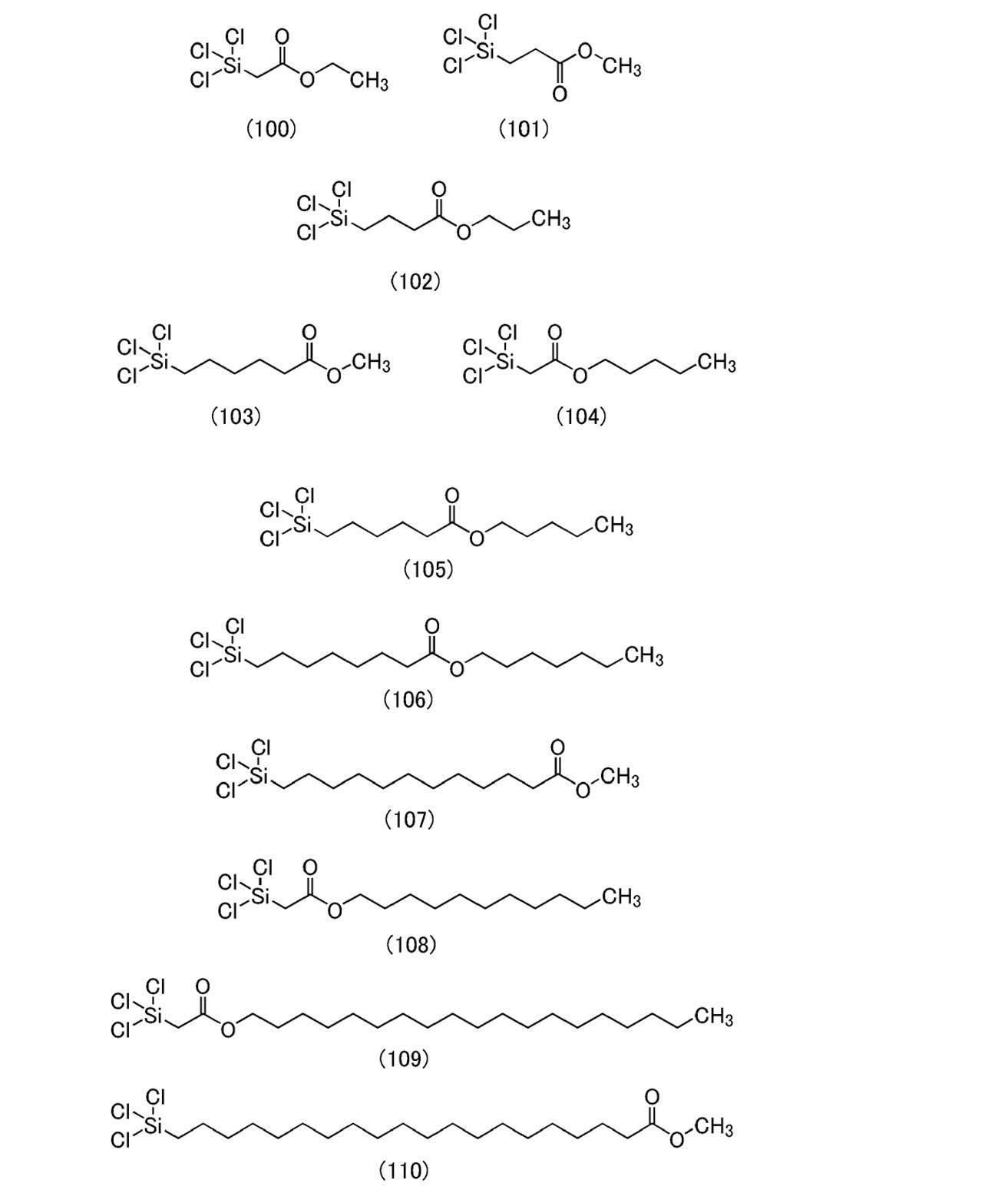
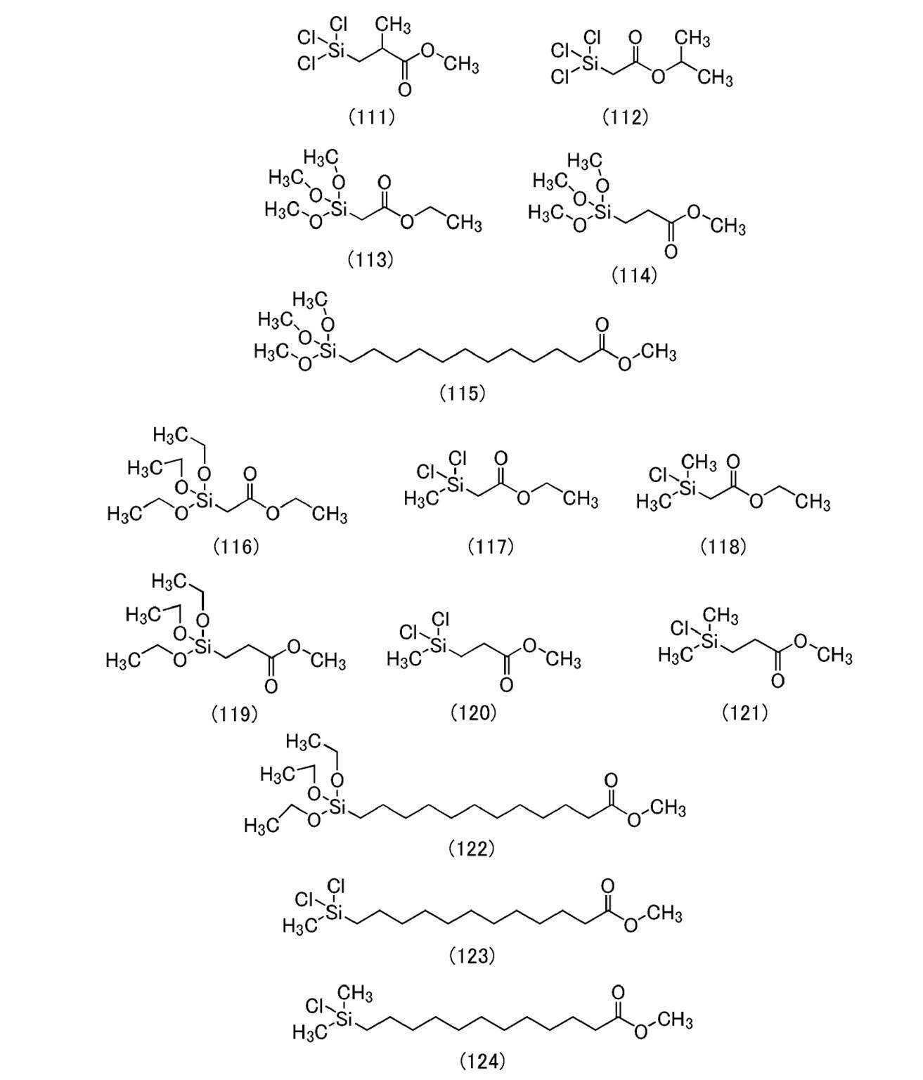

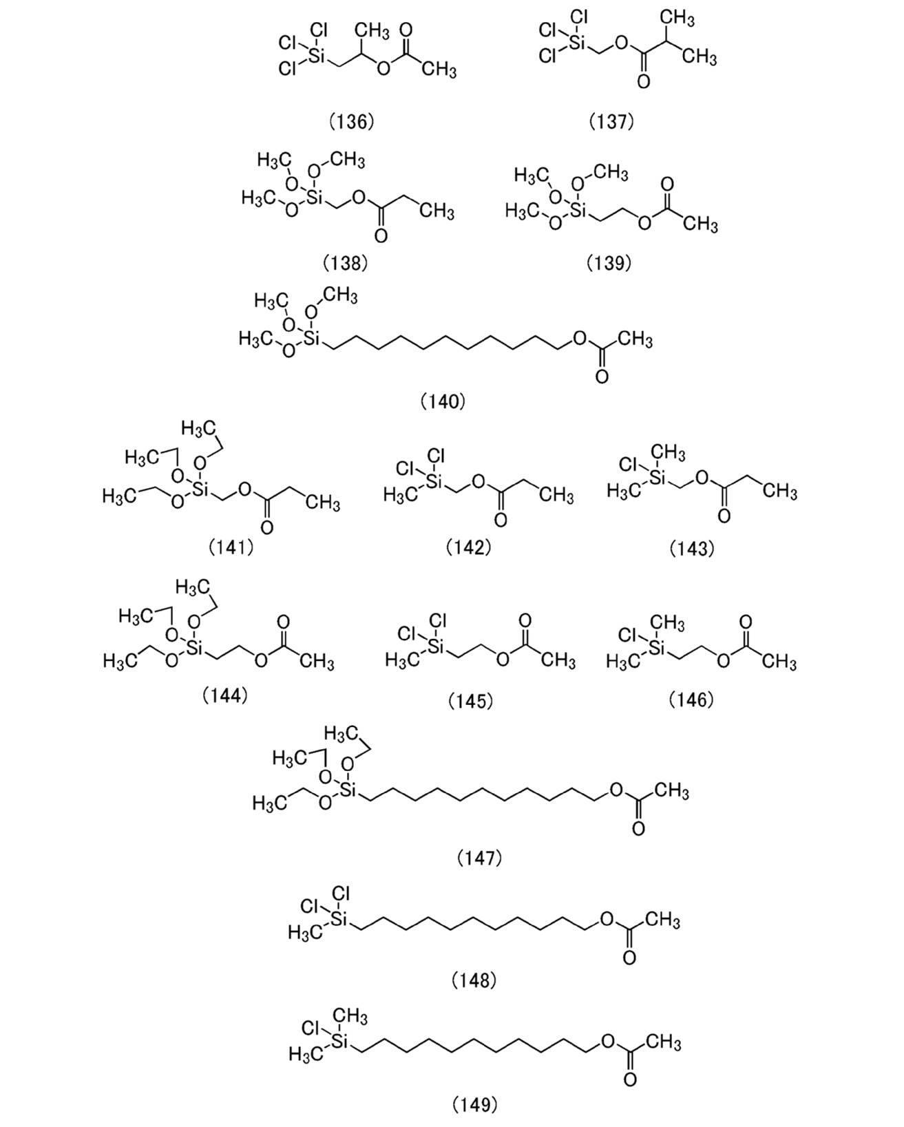

以上のようなケイ素化合物を用いることにより、少なくとも1つ以上のエステル基又はカルボキシル基を含む鎖状の基を有するグラフェン化合物を製造することができる。これらのケイ素化合物により化学修飾したグラフェン化合物は、電子伝導性が低く抑えられる一方でリチウムイオン伝導性が高いため、リチウムイオン蓄電池の固体電解質やセパレータに用いる材料として好適である。ただし、本発明の一態様に係るグラフェン化合物は、上述のようなケイ素化合物を用いて作製されることには限定されない。 By using the silicon compound as described above, a graphene compound having a chain-like group containing at least one ester group or a carboxyl group can be produced. Graphene compounds chemically modified with these silicon compounds have high electron conductivity and high lithium ion conductivity, and are therefore suitable as materials for solid electrolytes and separators of lithium ion storage batteries. However, the graphene compound according to one aspect of the present invention is not limited to being produced using the silicon compound as described above.
なお、本実施の形態において、本発明の一態様について述べた。または、他の実施の形態において、本発明の一態様について述べる。ただし、本発明の一態様は、これらに限定されない。例えば、本発明の一態様として、少なくとも1つ以上のエステル基又はカルボキシル基を含む鎖状の基を有するグラフェン化合物の例を示したが、本発明の一態様は、これに限定されない。 In the present embodiment, one aspect of the present invention has been described. Alternatively, in another embodiment, one aspect of the present invention will be described. However, one aspect of the present invention is not limited to these. For example, as one aspect of the present invention, an example of a graphene compound having a chain-like group containing at least one ester group or a carboxyl group has been shown, but one aspect of the present invention is not limited thereto.
なお、本実施の形態は、他の実施の形態と適宜組み合わせることが可能である。 It should be noted that this embodiment can be appropriately combined with other embodiments.
(実施の形態2)
本実施の形態では、本発明の一態様に係るグラフェン化合物を用いた蓄電装置として、リチウムイオン蓄電池の構成を説明する。
(Embodiment 2)
In the present embodiment, the configuration of a lithium ion storage battery will be described as a power storage device using the graphene compound according to one aspect of the present invention.
本発明の一態様にかかるリチウムイオン蓄電池110の作製方法について図1(A)及び図1(B)を用い、以下に説明する。図1(A)はリチウムイオン蓄電池110の外観図である。図1(B)は、図1(A)に示す一点鎖線B1-B2の断面図である。正極集電体100と、正極活物質層101と、固体電解質層であるグラフェン化合物105と、負極活物質層103と、負極集電体102と、が互いに重なり、外装体109により封止された状態の断面模式図である。なお、活物質層は集電体の両面に形成することもでき、リチウムイオン蓄電池を積層構造とすることも可能である。
A method for manufacturing the lithium
≪正極の構成≫
正極について説明する。正極は、正極活物質層101と、正極集電体100とを含む。
≪Construction of positive electrode≫
The positive electrode will be described. The positive electrode includes a positive electrode
正極活物質層101に用いられる正極活物質材料としては、リチウムイオン等のキャリアイオンの挿入及び脱離が可能な材料を用いることができ、例えば、オリビン型の結晶構造、層状岩塩型の結晶構造、又はスピネル型の結晶構造を有するリチウム含有材料等が挙げられる。
As the positive electrode active material used for the positive electrode
オリビン型構造のリチウム含有材料(一般式LiMPO4(Mは、Fe(II)、Mn(II)、Co(II)又はNi(II)))の代表例としては、LiFePO4、LiNiPO4、LiCoPO4、LiMnPO4、LiFeaNibPO4、LiFeaCobPO4、LiFeaMnbPO4、LiNiaCobPO4、LiNiaMnbPO4(a+bは1以下、0<a<1、0<b<1)、LiFecNidCoePO4、LiFecNidMnePO4、LiNicCodMnePO4(c+d+eは1以下、0<c<1、0<d<1、0<e<1)、LiFefNigCohMniPO4(f+g+h+iは1以下、0<f<1、0<g<1、0<h<1、0<i<1)等がある。 Typical examples of lithium-containing materials having an olivine structure (general formula LiMPO 4 (M is Fe (II), Mn (II), Co (II) or Ni (II))) are LiFePO 4 , LiNiPO 4 , and LiCoPO. 4 , LiMnPO 4 , LiFe a Ni b PO 4 , LiFe a Co b PO 4 , LiFe a Mn b PO 4 , LiNi a Co b PO 4 , LiNi a Mn b PO 4 (a + b is 1 or less, 0 <a <1 , 0 <b <1), LiFe c Ni d Co e PO 4 , LiFe c Ni d Mn e PO 4 , LiNi c Co d Mn e PO 4 (c + d + e is 1 or less, 0 <c <1, 0 <d < 1, 0 <e <1), LiFe f Ni g Coh Mn i PO 4 (f + g + h + i is 1 or less, 0 <f <1, 0 <g <1, 0 <h <1, 0 <i <1), etc. There is.
例えば、リン酸鉄リチウム(LiFePO4)は、安全性、安定性、高容量密度、高電位、初期酸化(充電)時に引き抜けるリチウムイオンの存在等、正極活物質に求められる事項をバランスよく満たしているため、好ましい。 For example, lithium iron phosphate (LiFePO 4 ) meets the requirements for a positive electrode active material in a well-balanced manner, such as safety, stability, high volume density, high potential, and the presence of lithium ions that are extracted during initial oxidation (charging). Therefore, it is preferable.
層状岩塩型の結晶構造を有するリチウム含有材料としては、例えば、コバルト酸リチウム(LiCoO2)、LiNiO2、LiMnO2、Li2MnO3、LiNi0.8Co0.2O2等のNiCo系(一般式は、LiNixCo1-xO2(0<x<1))、LiNi0.5Mn0.5O2等のNiMn系(一般式は、LiNixMn1-xO2(0<x<1))、LiNi1/3Mn1/3Co1/3O2等のNiMnCo系(NMCともいう。一般式は、LiNixMnyCo1-x-yO2(x>0、y>0、x+y<1))が挙げられる。さらに、Li(Ni0.8Co0.15Al0.05)O2、Li2MnO3-LiMO2(MはCo、Ni又はMn)等も挙げられる。 Examples of the lithium-containing material having a layered rock salt type crystal structure include NiCo-based materials such as lithium cobalt oxide (LiCoO 2 ), LiNiO 2 , LiMnO 2 , Li 2 MnO 3 , and LiNi 0.8 Co 0.2 O 2 . The general formula is a NiMn system such as LiNi x Co 1-x O 2 (0 <x <1)), LiNi 0.5 Mn 0.5 O 2 (general formula is LiNi x Mn 1-x O 2 (0). <X <1)), LiNi 1/3 Mn 1/3 Co 1/3 O 2 and other NiMnCo-based materials (also referred to as NMC. The general formula is LiNi x Mn y Co 1-x-y O 2 (x> 0). , Y> 0, x + y <1)). Further, Li (Ni 0.8 Co 0.15 Al 0.05 ) O 2 , Li 2 MnO 3 -LiMO 2 (M is Co, Ni or Mn) and the like can also be mentioned.
特に、LiCoO2は、容量が大きいこと、LiNiO2に比べて大気中で安定であること、LiNiO2に比べて熱的に安定であること等の利点があるため、好ましい。 In particular, LiCoO 2 is preferable because it has advantages such as a large capacity, stability in the atmosphere as compared with LiNiO 2 , and thermal stability as compared with LiNiO 2 .
スピネル型の結晶構造を有するリチウム含有材料としては、例えば、LiMn2O4、Li1+xMn2-xO4(0<x<2)、LiMn2-xAlxO4(0<x<2)、LiMn1.5Ni0.5O4等がある。 Examples of the lithium-containing material having a spinel-type crystal structure include LiMn 2 O 4 , Li 1 + x Mn 2-x O 4 (0 <x <2), and LiMn 2-x Al x O 4 (0 <x <2). ), LiMn 1.5 Ni 0.5 O 4 and the like.
LiMn2O4等のマンガンを含むスピネル型の結晶構造を有するリチウム含有材料に、少量のニッケル酸リチウム(LiNiO2やLiNi1-xMxO2(0<x<1)(M=Co、Al等))を混合すると、マンガンの溶出を抑制する、電解質の分解を抑制する等の利点があり好ましい。 A small amount of lithium nickelate (LiNiO 2 or LiNi 1-x M x O 2 (0 <x <1) (M = Co,) is added to a lithium-containing material having a spinel-type crystal structure containing manganese such as LiMn 2 O 4 . Mixing Al etc.)) has advantages such as suppressing the elution of manganese and suppressing the decomposition of the electrolyte, which is preferable.
また、正極活物質として、一般式Li(2-j)MSiO4(Mは、Fe(II)、Mn(II)、Co(II)、又はNi(II))(jは0以上2以下)で表される複合酸化物を用いることができる。一般式Li(2-j)MSiO4の代表例としては、Li(2-j)FeSiO4、Li(2-j)NiSiO4、Li(2-j)CoSiO4、Li(2-j)MnSiO4、Li(2-j)FekNilSiO4、Li(2-j)FekColSiO4、Li(2-j)FekMnlSiO4、Li(2-j)NikColSiO4、Li(2-j)NikMnlSiO4(k+lは1以下、0<k<1、0<l<1)、Li(2-j)FemNinCoqSiO4、Li(2-j)FemNinMnqSiO4、Li(2-j)NimConMnqSiO4(m+n+qは1以下、0<m<1、0<n<1、0<q<1)、Li(2-j)FerNisCotMnuSiO4(r+s+t+uは1以下、0<r<1、0<s<1、0<t<1、0<u<1)等が挙げられる。 Further, as the positive electrode active material, the general formula Li (2-j) MSiO 4 (M is Fe (II), Mn (II), Co (II), or Ni (II)) (j is 0 or more and 2 or less). A composite oxide represented by is used. Typical examples of the general formula Li (2-j) MSiO 4 are Li (2-j) FeSiO 4 , Li (2-j) NiSiO 4 , Li (2-j) CoSiO 4 , Li (2-j) MnSiO. 4 , Li (2-j) Fe k Ni l SiO 4 , Li (2-j) Fe k Co l SiO 4 , Li (2-j) Fe k Mn l SiO 4 , Li (2-j) Ni k Co l SiO 4 , Li (2-j) Ni k Mn l SiO 4 (k + l is 1 or less, 0 <k <1, 0 <l <1), Li (2-j) Fe m Ni n Co q SiO 4 , Li (2-j) Fe m Ni n Mn q SiO 4 , Li (2-j) Ni m Con n Mn q SiO 4 (m + n + q is 1 or less, 0 <m <1, 0 <n <1, 0 <q <1), Li (2-j) Ferr Nis Cot Mn u SiO 4 ( r + s + t + u is 1 or less, 0 <r <1, 0 <s <1, 0 <t <1, 0 <u <1) And so on.
また、正極活物質として、AxM2(XO4)3(AはLi、Na、又はMg)(MはFe、Mn、Ti、V、Nb、又はAl)(XはS、P、Mo、W、As、又はSi)の一般式で表されるナシコン型化合物を用いることができる。ナシコン型化合物としては、Fe2(MnO4)3、Fe2(SO4)3、Li3Fe2(PO4)3等が挙げられる。また、正極活物質として、Li2MPO4F、Li2MP2O7、Li5MO4(MはFe又はMn)の一般式で表される化合物、NaFeF3、FeF3等のペロブスカイト型フッ化物、TiS2、MoS2等の金属カルコゲナイド(硫化物、セレン化物、テルル化物)、LiMVO4等の逆スピネル型の結晶構造を有するリチウム含有材料、バナジウム酸化物系(V2O5、V6O13、LiV3O8等)、マンガン酸化物、有機硫黄等の材料を用いることができる。 Further, as the positive electrode active material, A x M 2 (XO 4 ) 3 (A is Li, Na, or Mg) (M is Fe, Mn, Ti, V, Nb, or Al) (X is S, P, Mo). , W, As, or Si) can be used as a nacicon type compound represented by the general formula. Examples of the pear-con type compound include Fe 2 (MnO 4 ) 3 , Fe 2 (SO 4 ) 3 , Li 3 Fe 2 (PO 4 ) 3 and the like. Further, as the positive electrode active material, a compound represented by the general formula of Li 2 MPO 4 F, Li 2 MP 2 O 7 , Li 5 MO 4 (M is Fe or Mn), NaFeF 3 , FeF 3 , etc. Chemicals, metal chalcogenides (sulfides, seleniums, tellurides) such as TiS 2 , MoS 2 , lithium-containing materials having an inverted spinel-type crystal structure such as LiMVO 4 , vanadium oxide-based (V 2 O 5 , V 6 ). Materials such as O 13 , LiV 3 O 8 ), manganese oxide, and organic sulfur can be used.
なお、キャリアイオンが、リチウムイオン以外のアルカリ金属イオンや、アルカリ土類金属イオンの場合、正極活物質として、上記化合物や酸化物において、リチウムの代わりに、アルカリ金属(例えば、ナトリウムやカリウム等)、アルカリ土類金属(例えば、カルシウム、ストロンチウム、バリウム、ベリリウム、マグネシウム等)を用いてもよい。例えば、NaFeO2や、Na2/3[Fe1/2Mn1/2]O2などのナトリウム含有層状酸化物を正極活物質として用いることができる。 When the carrier ion is an alkali metal ion other than lithium ion or an alkaline earth metal ion, the above compound or oxide may be an alkali metal (for example, sodium or potassium) instead of lithium as a positive electrode active material. , Alkaline earth metals (eg, calcium, strontium, barium, beryllium, magnesium, etc.) may be used. For example, sodium-containing layered oxides such as NaFeO 2 and Na 2/3 [Fe 1/2 Mn 1/2 ] O 2 can be used as the positive electrode active material.
また、正極活物質として、上記材料を複数組み合わせた材料を用いてもよい。例えば、上記材料を複数組み合わせた固溶体を正極活物質として用いることができる。例えば、LiCo1/3Mn1/3Ni1/3O2とLi2MnO3の固溶体を正極活物質として用いることができる。 Further, as the positive electrode active material, a material obtained by combining a plurality of the above materials may be used. For example, a solid solution in which a plurality of the above materials are combined can be used as a positive electrode active material. For example, solid solutions of LiCo 1/3 Mn 1/3 Ni 1/3 O 2 and Li 2 MnO 3 can be used as the positive electrode active material.
正極活物質は、一次粒子の平均粒径が50nm以上100μm以下のものを用いるとよい。 As the positive electrode active material, it is preferable to use a positive electrode active material having an average particle size of primary particles of 50 nm or more and 100 μm or less.
正極活物質は負極活物質と共に、蓄電装置の電池反応の中心的役割を担いキャリアイオンの放出及び吸収を行う物質である。蓄電装置の寿命を高めるためには、電池反応の不可逆反応に係る容量が小さい材料であることが好ましく、充放電効率の高い材料であることが好ましい。 The positive electrode active material, together with the negative electrode active material, is a substance that plays a central role in the battery reaction of the power storage device and releases and absorbs carrier ions. In order to extend the life of the power storage device, it is preferable that the material has a small capacity related to the irreversible reaction of the battery reaction, and it is preferable that the material has a high charge / discharge efficiency.
活物質は電解質と接するため、活物質と電解質とが反応し、反応により活物質が失われ劣化すると、蓄電装置の容量が低下するため、劣化の少ない蓄電装置を実現するためには、蓄電装置内のこのような反応が生じないことが望ましい。 Since the active material comes into contact with the electrolyte, the active material reacts with the electrolyte, and when the active material is lost and deteriorates due to the reaction, the capacity of the power storage device decreases. It is desirable that such a reaction does not occur.
電極の導電助剤として、アセチレンブラック(AB)、グラファイト(黒鉛)粒子、カーボンナノチューブ、グラフェン、フラーレンなどを用いることができる。 As the conductive auxiliary agent for the electrode, acetylene black (AB), graphite particles, carbon nanotubes, graphene, fullerene and the like can be used.
導電助剤により、電極中に電子伝導のネットワークを形成することができる。導電助剤により、正極活物質どうしの電子伝導の経路を維持することができる。正極活物質層中に導電助剤を添加することにより、高い電子伝導性を有する正極活物質層101を実現することができる。
The conductive auxiliary agent can form a network of electron conduction in the electrode. The conductive auxiliary agent can maintain the path of electron conduction between the positive electrode active materials. By adding a conductive additive to the positive electrode active material layer, the positive electrode
また、バインダーとして、代表的なポリフッ化ビニリデン(PVDF)の他、ポリイミド、ポリテトラフルオロエチレン、ポリビニルクロライド、エチレンプロピレンジエンポリマー、フッ素ゴム、ポリメチルメタクリレート、ポリエチレン、ニトロセルロース等を用いることができる。 Further, as the binder, in addition to typical polyvinylidene fluoride (PVDF), polyimide, polytetrafluoroethylene, polyvinyl chloride, ethylene propylene diene polymer, fluororubber, polymethylmethacrylate, polyethylene, nitrocellulose and the like can be used.
正極活物質層101の総量に対するバインダーの含有量は、0.5wt%以上10wt%以下が好ましく、2wt%以上8wt%以下がより好ましく、3wt%以上5wt%以下がさらに好ましい。また、正極活物質層101の総量に対する導電助剤の含有量は、1wt%以上10wt%以下が好ましく、1wt%以上5wt%以下がより好ましい。
The content of the binder with respect to the total amount of the positive electrode
塗布法を用いて正極活物質層101を形成する場合は、正極活物質とバインダーと導電助剤と分散媒を混合して電極スラリーを作製し、正極集電体100上に塗布して乾燥させればよい。
When the positive electrode
また、正極活物質層101はスパッタ法などにより薄膜状に形成してもよい。
Further, the positive electrode
なお、正極集電体100にはステンレス、金、白金、アルミニウム、チタン等の金属、及びこれらの合金など、電子伝導性の高い材料を用いることができる。また、シリコン、チタン、ネオジム、スカンジウム、モリブデンなどの耐熱性を向上させる元素が添加されたアルミニウム合金を用いることができる。また、シリコンと反応してシリサイドを形成する金属元素で形成してもよい。シリコンと反応してシリサイドを形成する金属元素としては、ジルコニウム、チタン、ハフニウム、バナジウム、ニオブ、タンタル、クロム、モリブデン、タングステン、コバルト、ニッケル等がある。正極集電体は、箔状、板状(シート状)、網状、パンチングメタル状、エキスパンドメタル状等の形状を適宜用いることができる。
For the positive electrode
以上の工程でリチウムイオン蓄電池の正極を作製することができる。 The positive electrode of the lithium ion storage battery can be manufactured by the above steps.
≪負極の構成≫
次に負極について説明する。負極は、負極活物質層103と、負極集電体102とを含む。負極を形成する工程を以下に説明する。
≪Construction of negative electrode≫
Next, the negative electrode will be described. The negative electrode includes a negative electrode
負極活物質層103に用いられる負極活物質として、炭素系材料としては、黒鉛、易黒鉛化性炭素(ソフトカーボン)、難黒鉛化性炭素(ハードカーボン)、カーボンナノチューブ、グラフェン、カーボンブラック等がある。黒鉛としては、メソカーボンマイクロビーズ(MCMB)、コークス系人造黒鉛、ピッチ系人造黒鉛等の人造黒鉛や、球状化天然黒鉛等の天然黒鉛がある。また、黒鉛の形状としては鱗片状のものや球状のものなどがある。
As the negative electrode active material used for the negative electrode
負極活物質として、炭素系材料以外に、リチウムとの合金化・脱合金化反応により充放電反応を行うことが可能な材料も用いることができる。例えば、Ga、Si、Al、Ge、Sn、Pb、Sb、Bi、Ag、Zn、Cd、In等のうち少なくとも一つを含む材料を用いることができる。このような元素は炭素と比べて容量が大きく、特にシリコンは理論容量が4200mAh/gと高く好ましい。このような元素を用いた合金系材料としては、例えば、Mg2Si、Mg2Ge、Mg2Sn、SnS2、V2Sn3、FeSn2、CoSn2、Ni3Sn2、Cu6Sn5、Ag3Sn、Ag3Sb、Ni2MnSb、CeSb3、LaSn3、La3Co2Sn7、CoSb3、InSb、SbSn等がある。 As the negative electrode active material, in addition to the carbon-based material, a material capable of performing a charge / discharge reaction by an alloying / dealloying reaction with lithium can also be used. For example, a material containing at least one of Ga, Si, Al, Ge, Sn, Pb, Sb, Bi, Ag, Zn, Cd, In and the like can be used. Such an element has a larger capacity than carbon, and silicon is particularly preferable because it has a theoretical capacity of 4200 mAh / g. Examples of alloy-based materials using such elements include Mg 2 Si, Mg 2 Ge, Mg 2 Sn, SnS 2 , V2 Sn 3 , FeSn 2 , CoSn 2 , Ni 3 Sn 2 , and Cu 6 Sn 5 . , Ag 3 Sn, Ag 3 Sb, Ni 2 MnSb, CeSb 3 , LaSn 3 , La 3 Co 2 Sn 7 , CoSb 3 , InSb, SbSn and the like.
また、負極活物質として、SiO、SnO、SnO2、二酸化チタン(TiO2)、リチウムチタン酸化物(Li4Ti5O12)、リチウム-黒鉛層間化合物(LixC6)、五酸化ニオブ(Nb2O5)、酸化タングステン(WO2)、酸化モリブデン(MoO2)等の酸化物を用いることができる。 Further, as the negative electrode active material, SiO, SnO, SnO 2 , titanium dioxide (TIO 2 ), lithium titanium oxide (Li 4 Ti 5 O 12 ), lithium-graphite interlayer compound (Li x C 6 ), niobium pentoxide (Li x C 6) Oxides such as Nb 2 O 5 ), titanium oxide (WO 2 ) and molybdenum oxide (MoO 2 ) can be used.
また、負極活物質として、リチウムと遷移金属の複窒化物である、Li3N型構造をもつLi(3-x)MxN(MはCo、Ni又はCu)を用いることができる。例えば、Li2.6Co0.4N3は大きな充放電容量(900mAh/g、1890mAh/cm3)を示し好ましい。 Further, as the negative electrode active material, Li ( 3 -x) M x N (M is Co, Ni or Cu) having a Li 3N type structure, which is a double nitride of lithium and a transition metal, can be used. For example, Li 2.6 Co 0.4 N 3 shows a large charge / discharge capacity (900 mAh / g, 1890 mAh / cm 3 ) and is preferable.
リチウムと遷移金属の複窒化物を用いると、負極活物質中にリチウムを含むため、正極活物質としてリチウムを含まないV2O5、Cr3O8等の材料と組み合わせることができる。なお、正極活物質にリチウムを含む材料を用いる場合でも、あらかじめ正極活物質に含まれるリチウムを脱離させることで、負極活物質としてリチウムと遷移金属の複窒化物を用いることができる。 When a double nitride of lithium and a transition metal is used, since lithium is contained in the negative electrode active material, it can be combined with materials such as V2 O 5 and Cr 3 O 8 which do not contain lithium as the positive electrode active material. Even when a material containing lithium is used as the positive electrode active material, a double nitride of lithium and a transition metal can be used as the negative electrode active material by desorbing lithium contained in the positive electrode active material in advance.
また、コンバージョン反応が生じる材料を負極活物質として用いることもできる。例えば、酸化コバルト(CoO)、酸化ニッケル(NiO)、酸化鉄(FeO)等の、リチウムと合金化反応を行わない遷移金属酸化物を負極活物質に用いてもよい。コンバージョン反応が生じる材料としては、さらに、Fe2O3、CuO、Cu2O、RuO2、Cr2O3等の酸化物、CoS0.89、NiS、CuS等の硫化物、Zn3N2、Cu3N、Ge3N4等の窒化物、NiP2、FeP2、CoP3等のリン化物、FeF3、BiF3等のフッ化物でも起こる。 Further, a material that causes a conversion reaction can also be used as a negative electrode active material. For example, a transition metal oxide that does not undergo an alloying reaction with lithium, such as cobalt oxide (CoO), nickel oxide (NiO), and iron oxide (FeO), may be used as the negative electrode active material. Materials that cause a conversion reaction include oxides such as Fe 2 O 3 , CuO, Cu 2 O, RuO 2 , Cr 2 O 3 , sulfides such as CoS 0.89 , NiS, and CuS, and Zn 3 N 2 . , Cu 3 N, Ge 3 N 4 , etc., phosphodies such as NiP 2 , FeP 2 , CoP 3 , etc., and fluorides such as FeF 3 , BiF 3 etc. also occur.
負極活物質は、一例としては、粒径が50nm以上100μm以下のものを用いるとよい。 As an example, the negative electrode active material may have a particle size of 50 nm or more and 100 μm or less.
なお、正極活物質層101においても負極活物質層103においても、活物質材料は複数の材料を特定の割合で組み合わせて用いてもよい。活物質層に複数の材料を用いることで、より詳細に活物質層の性能を選択することができる。
In both the positive electrode
電極の導電助剤として、アセチレンブラック(AB)、グラファイト(黒鉛)粒子、カーボンナノチューブ、グラフェン、フラーレンなどを用いることができる。 As the conductive auxiliary agent for the electrode, acetylene black (AB), graphite particles, carbon nanotubes, graphene, fullerene and the like can be used.
導電助剤により、電極中に電子伝導のネットワークを形成することができる。導電助剤により、負極活物質どうしの電子伝導の経路を維持することができる。負極活物質層中に導電助剤を添加することにより、高い電子伝導性を有する負極活物質層103を実現することができる。
The conductive auxiliary agent can form a network of electron conduction in the electrode. The conductive auxiliary agent can maintain the path of electron conduction between the negative electrode active materials. By adding a conductive auxiliary agent to the negative electrode active material layer, the negative electrode
また、バインダーとして、代表的なポリフッ化ビニリデン(PVDF)の他、ポリイミド、ポリビニルクロライド、エチレンプロピレンジエンポリマー、スチレン-ブタジエンゴム、カルボキシメチルセルロースナトリウム、アクリロニトリル-ブタジエンゴム、フッ素ゴム、ポリ酢酸ビニル、ポリメチルメタクリレート、ポリエチレン、ニトロセルロース等を用いることができる。 As a binder, in addition to typical polyvinylidene fluoride (PVDF), polyimide, polyvinyl chloride, ethylene propylene diene polymer, styrene-butadiene rubber, sodium carboxymethyl cellulose, acrylonitrile-butadiene rubber, fluororubber, polyvinyl acetate, polymethyl. Methacrylate, polyethylene, nitrocellulose and the like can be used.
負極活物質層103の総量に対するバインダーの含有量は、1wt%以上10wt%以下が好ましく、2wt%以上8wt%以下がより好ましく、3wt%以上5wt%以下がさらに好ましい。また、負極活物質層103の総量に対する導電助剤の含有量は、1wt%以上10wt%以下が好ましく、1wt%以上5wt%以下がより好ましい。
The content of the binder with respect to the total amount of the negative electrode
次いで、負極集電体102上に負極活物質層103を形成する。塗布法を用いて負極活物質層103を形成する場合は、負極活物質とバインダーと導電助剤と分散媒を混合してスラリーを作製し、負極集電体102に塗布して乾燥させる。また、乾燥後に必要があればプレス処理を行ってもよい。
Next, the negative electrode
また、負極活物質層103はスパッタ法などにより薄膜状に形成してもよい。
Further, the negative electrode
なお、負極集電体102には、ステンレス、金、白金、鉄、銅、チタン、タンタル等の金属、及びこれらの合金など、電子伝導性が高く、リチウム等のキャリアイオンと合金化しない材料を用いることができる。また、シリコンと反応してシリサイドを形成する金属元素で形成してもよい。シリコンと反応してシリサイドを形成する金属元素としては、ジルコニウム、チタン、ハフニウム、バナジウム、ニオブ、タンタル、クロム、モリブデン、タングステン、コバルト、ニッケル等がある。負極集電体102は、箔状、板状(シート状)、網状、円柱状、コイル状、パンチングメタル状、エキスパンドメタル状等の形状を適宜用いることができる。負極集電体102は、厚みが5μm以上30μm以下のものを用いるとよい。また、電極集電体の表面の一部に、グラファイトなどを用いてアンダーコート層を設けてもよい。また、負極活物質としてリチウムチタン酸化物(Li4Ti5O12)のような高電位材料を使用する場合、負極集電体102にアルミニウムを用いることができる。
The negative electrode
以上の工程でリチウムイオン蓄電池の負極を作製することができる。 The negative electrode of the lithium ion storage battery can be manufactured by the above steps.
≪固体電解質層の構成≫
本発明の一態様に係るグラフェン化合物を固体電解質層に用いる場合、該グラフェン化合物にリチウム塩を混合して用いてもよい。
≪Structure of solid electrolyte layer≫
When the graphene compound according to one aspect of the present invention is used for the solid electrolyte layer, a lithium salt may be mixed with the graphene compound and used.
例えば、本発明の一態様に係るグラフェン化合物をテトラヒドロフラン(THF)に分散させた分散液と、リチウム塩をTHFに分散させた溶液と、を混合する。次に、これを、固体電解質層を形成する材料に1又は複数滴を滴下し、ホットプレート上で簡易的に乾燥し、その後90℃の温度にて減圧下乾燥して固体電解質層を形成する。当該固体電解質層はフィルム状となる場合がある。当該固体電解質層を正極と負極との間に挟み、外装体に収納する。 For example, a dispersion in which the graphene compound according to one aspect of the present invention is dispersed in tetrahydrofuran (THF) and a solution in which a lithium salt is dispersed in THF are mixed. Next, one or more drops of this are dropped onto the material forming the solid electrolyte layer, and the mixture is simply dried on a hot plate and then dried under reduced pressure at a temperature of 90 ° C. to form a solid electrolyte layer. .. The solid electrolyte layer may be in the form of a film. The solid electrolyte layer is sandwiched between the positive electrode and the negative electrode and stored in the exterior body.
本発明の一態様に係るグラフェン化合物は、エステル基又はカルボキシル基を含む官能基を有することから、溶媒への分散性が高い。溶媒への分散性が高いことから、上記方法で固体電解質層を形成する際に、フィルム状に形成しやすい。 Since the graphene compound according to one aspect of the present invention has a functional group containing an ester group or a carboxyl group, it has high dispersibility in a solvent. Since it has high dispersibility in a solvent, it is easy to form a film when the solid electrolyte layer is formed by the above method.
例えば、リチウム塩として、LiPF6、LiClO4、LiAsF6、LiBF4、LiAlCl4、LiSCN、LiBr、LiI、Li2SO4、Li2B10Cl10、Li2B12Cl12、LiCF3SO3、LiC4F9SO3、LiC(CF3SO2)3、LiC(C2F5SO2)3、LiN(CF3SO2)2、LiN(C4F9SO2)(CF3SO2)、LiN(C2F5SO2)2等から選ばれた一又は複数を用いることができる。 For example, as lithium salts, LiPF 6 , LiClO 4 , LiAsF 6 , LiBF 4 , LiAlCl 4 , LiSCN, LiBr, LiI, Li 2 SO 4 , Li 2 B 10 Cl 10 , Li 2 B 12 Cl 12 , LiCF 3 SO 3 , LiC 4 F 9 SO 3 , LiC (CF 3 SO 2 ) 3 , LiC (C 2 F 5 SO 2 ) 3 , LiN (CF 3 SO 2 ) 2 , LiN (C 4 F 9 SO 2 ) (CF 3 SO) 2 ) One or more selected from LiN (C 2 F 5 SO 2 ) 2 and the like can be used.
なお、本発明の一態様に係るグラフェン化合物を固体電解質層に用いるためのリチウム塩の混合方法は、これに限定されない。 The method for mixing the lithium salt for using the graphene compound according to one aspect of the present invention in the solid electrolyte layer is not limited to this.
また、前述のリチウム塩を混合したグラフェン化合物に、酸化物系固体電解質、硫化物系固体電解質またはポリマー電解質の一以上を混合し、それを固体電解質層として使用してもよい。 Further, one or more of the oxide-based solid electrolyte, the sulfide-based solid electrolyte, or the polymer electrolyte may be mixed with the graphene compound mixed with the above-mentioned lithium salt, and the solid electrolyte layer may be used.
例えば、酸化物系電解質として、La0.51Li0.34TiO2.94、Li1.3Al0.3Ti1.7(PO4)3、Li7La3Zr2O12、50Li4SiO4・50Li3BO3、Li2.9PO3.3N0.46、Li3.6Si0.6P0.4O4、Li1.07Al0.69Ti1.46(PO4)3、Li1.5Al0.5Ge1.5(PO4)3等から選ばれた一又は複数を用いることができる。 For example, as an oxide-based electrolyte, La 0.51 Li 0.34 TIO 2.94 , Li 1.3 Al 0.3 Ti 1.7 (PO 4 ) 3 , Li 7 La 3 Zr 2 O 12 , 50Li 4 SiO 4.50 Li 3 BO 3 , Li 2.9 PO 3.3 N 0.46 , Li 3.6 Si 0.6 P 0.4 O 4 , Li 1.07 Al 0.69 Ti 1.46 (PO) 4 ) One or more selected from 3 , Li 1.5 Al 0.5 Ge 1.5 (PO 4 ) 3 and the like can be used.
例えば、硫化物系電解質として、Li10GeP2S12、Li3.25Ge0.25P0.75S4、30Li2S・26B2S3・44LiI、63Li2S・36SiS2・1Li3PO4、57Li2S・38SiS2・5Li4SiO4、70Li2S・30P2S5、50Li2S・50GeS2、Li7P3S11、Li3.25P0.95S4等から選ばれた一又は複数を用いることができる。 For example, as sulfide-based electrolytes, Li 10 GeP 2 S 12 , Li 3.25 Ge 0.25 P 0.75 S 4 , 30Li 2 S ・ 26B 2 S 3.44LiI, 63Li 2 S ・36SiS 2.1Li 3 From PO 4 , 57Li 2 S / 38SiS 2.5Li 4 SiO 4 , 70Li 2 S / 30P 2 S 5 , 50Li 2 S / 50GeS 2 , Li 7 P 3 S 11 , Li 3.25 P 0.95 S 4 , etc. One or more selected ones can be used.
例えば、ポリマー電解質として、ポリエチレンオキシド、ポリプロピレンオキシド、ポリエチレンイミン等から選ばれた一又は複数を用いることができる。また、ポリマー電解質にリチウム塩を溶解させたものを用いることもできる。 For example, as the polymer electrolyte, one or more selected from polyethylene oxide, polypropylene oxide, polyethyleneimine and the like can be used. Further, a polymer electrolyte in which a lithium salt is dissolved can also be used.
固体電解質層は複数層としてもよい。すなわち、第1の固体電解質層及び第2の固体電解質層をそれぞれ異なる方法で作製し、これを併せて蓄電装置に用いることができる。また、第1の固体電解質層及び第2の固体電解質層は同じ方法で作製してもよい。 The solid electrolyte layer may be a plurality of layers. That is, the first solid electrolyte layer and the second solid electrolyte layer can be produced by different methods, and these can be used together in the power storage device. Further, the first solid electrolyte layer and the second solid electrolyte layer may be produced by the same method.
さらに、蓄電装置が可撓性を有していてもよく、可撓性を有する蓄電装置に変形応力がかかる場合にも、第1の固体電解質層と第2の固体電解質層との界面において、両方の固体電解質層が摺動することにより応力を緩和することができるため、複数の固体電解質層を用いた構造は、可撓性を有する蓄電装置の固体電解質層の構造としても適している。 Further, the power storage device may have flexibility, and even when the flexible power storage device is subjected to deformation stress, at the interface between the first solid electrolyte layer and the second solid electrolyte layer, Since the stress can be relieved by sliding both solid electrolyte layers, the structure using a plurality of solid electrolyte layers is also suitable as the structure of the solid electrolyte layer of the flexible power storage device.
≪セパレータの構成≫
セパレータについて説明する。セパレータは、両極の接触を防ぐ絶縁性能と、イオンの伝導性がなければならない。
≪Construction of separator≫
The separator will be described. The separator must have insulation performance to prevent contact between the two poles and ionic conductivity.
固体電池においては、固体電解質層がセパレータの機能を兼ね備えていてもよい。セパレータの材料として、本発明の一態様に係る固体電解質層となるグラフェン化合物を使用することができる(図1(B)参照)。 In the solid-state battery, the solid electrolyte layer may also have the function of a separator. As the material of the separator, a graphene compound serving as a solid electrolyte layer according to one aspect of the present invention can be used (see FIG. 1 (B)).
また、固体電解質層となるグラフェン化合物とは別に、セパレータも使用してもよい。セパレータの材料として、フッ素系ポリマー、ポリエチレンオキシド、ポリプロピレンオキシド等のポリエーテル、ポリエチレン、ポリプロピレン等のポリオレフィン、ポリアクリロニトリル、ポリ塩化ビニリデン、ポリメチルメタクリレート、ポリメチルアクリレート、ポリビニルアルコール、ポリメタクリロニトリル、ポリビニルアセテート、ポリビニルピロリドン、ポリエチレンイミン、ポリブタジエン、ポリスチレン、ポリイソプレン、ポリウレタン系高分子及びこれらの誘導体、セルロース、紙、不織布、ガラス繊維から選ばれる一種を単独で、又は二種以上を組み合せて用いることができる。特性の異なる二つのセパレータを併せて用いることにより、一方のセパレータを単独で用いる場合と比べ、蓄電装置のセパレータの性能を多彩に選択することができるようになる。 In addition to the graphene compound that becomes the solid electrolyte layer, a separator may also be used. As the material of the separator, fluoropolymer, polyethylene oxide, polyether such as polypropylene oxide, polyolefin such as polyethylene and polypropylene, polyacrylonitrile, polyvinylidene chloride, polymethylmethacrylate, polymethylacrylate, polyvinyl alcohol, polymethacrylonitrile, polyvinyl One selected from acetate, polyvinylpyrrolidone, polyethyleneimine, polybutadiene, polystyrene, polyisoprene, polyurethane polymers and derivatives thereof, cellulose, paper, non-woven fabrics, and glass fibers can be used alone or in combination of two or more. can. By using two separators having different characteristics together, it becomes possible to select various performances of the separator of the power storage device as compared with the case where one separator is used alone.
次に、固体電解質層及びセパレータを蓄電装置に組み込む方法としては、固体電解質層及びセパレータを、正極及び負極の間に挟みこむ方法が可能である。また、正極又は負極の一方に固体電解質層及びセパレータを載置し、正極又は負極のもう一方を併せる方法も可能である。正極、負極、固体電解質層及びセパレータを外装体に収納することにより、蓄電装置を形成することができる。 Next, as a method of incorporating the solid electrolyte layer and the separator into the power storage device, a method of sandwiching the solid electrolyte layer and the separator between the positive electrode and the negative electrode is possible. It is also possible to place a solid electrolyte layer and a separator on one of the positive electrode and the negative electrode and combine the other of the positive electrode and the negative electrode. A power storage device can be formed by housing the positive electrode, the negative electrode, the solid electrolyte layer, and the separator in the exterior body.
固体電解質層及びセパレータを組み込んだリチウムイオン蓄電池120の構造を示す模式図を図2に示す。図2は正極活物質層101、負極活物質層103、固体電解質層であるグラフェン化合物105及びセパレータ107を拡大した図である。正極活物質層101と負極活物質層103の間に、固体電解質層であるグラフェン化合物105及びセパレータ107は配置される。セパレータ107の繊維の隙間に固体電解質層であるグラフェン化合物105が埋まっており、固体電解質層であるグラフェン化合物105は正極活物質層101及び負極活物質層103と接触している。この様な構造にすることにより、正極と負極の短絡を防ぐ効果が高くなるので好ましい。なお、例として繊維状のセパレータを示したが、セパレータの形状はこれに限られない。
FIG. 2 shows a schematic diagram showing the structure of the lithium
また、固体電解質層及びセパレータを正極又は負極の一方の両面を覆うことができる大きさのシート状若しくはエンベロープ状に形成し、固体電解質層及びセパレータに包まれた電極とすると、蓄電装置の製造上、電極を機械的な損傷から保護することができ、電極の取り扱いが容易となる。固体電解質層及びセパレータに包まれた電極ともう一方の電極とを、併せて外装体に収納することにより、蓄電装置を形成することができる。 Further, if the solid electrolyte layer and the separator are formed in a sheet shape or an envelope shape having a size capable of covering both sides of the positive electrode or the negative electrode, and the electrode is wrapped in the solid electrolyte layer and the separator, the storage device can be manufactured. , The electrode can be protected from mechanical damage, and the electrode can be easily handled. A power storage device can be formed by accommodating the electrode wrapped in the solid electrolyte layer and the separator and the other electrode together in the exterior body.
さらに、セパレータ107及びグラフェン化合物105はそれぞれ複数層としてもよい。例えば、第1のセパレータ、第1の固体電解質層であるグラフェン化合物、第2のセパレータ、第2の固体電解質層であるグラフェン化合物をこの順で重ねてもよい。複数層用いる場合、セパレータ107の繊維の隙間に固体電解質層であるグラフェン化合物105が埋まり、固体電解質層であるグラフェン化合物105は正極活物質層101及び負極活物質層103と接触させるようにしてもよい。
Further, the
さらに、蓄電装置が可撓性を有していてもよく、可撓性を有する蓄電装置に変形応力がかかる場合にも、第1のセパレータと第2のセパレータとの界面において、両セパレータが摺動することにより応力を緩和することができるため、複数のセパレータを用いた構造は、可撓性を有する蓄電装置のセパレータの構造としても適している。 Further, the power storage device may have flexibility, and even when the flexible power storage device is subjected to deformation stress, both separators slide at the interface between the first separator and the second separator. Since the stress can be relieved by moving, a structure using a plurality of separators is also suitable as a structure for a separator of a flexible power storage device.
以上の工程でリチウムイオン蓄電池にセパレータを組み込むことができる。 In the above process, the separator can be incorporated into the lithium ion storage battery.
≪外装体の構成≫
次に、外装体109について説明する。外装体109には、例えばポリエチレン、ポリプロピレン、ポリカーボネート、アイオノマー、ポリアミド等の材料を有する膜上に、アルミニウム、ステンレス、銅、ニッケル等の可撓性に優れた金属薄膜を設け、さらに該金属薄膜上に外装体の外面としてポリアミド系樹脂、ポリエステル系樹脂等の絶縁性合成樹脂膜を設けた三層構造のフィルムを用いることができる。このような三層構造とすることで、電解質や気体の透過を遮断するとともに、絶縁性を確保し、併せて耐電解質性を有する。耐電解質性とは、電解質によって腐食しないことを示す。外装体を内側に折り曲げて重ねて、又は、2つの外装体それぞれの内面を向い合せて重ねて熱を加えることにより、内面の材料が融け2つの外装体を融着することができ、封止構造を作製することができる。
≪Structure of exterior body≫
Next, the
外装体が融着等され封止構造が形成されている箇所を封止部とすると、外装体を内側に折り曲げて重ねた場合は、折り目以外の箇所に封止部が形成され、外装体の第1の領域と、該第1の領域と重なる第2の領域とが融着等された構造となる。また、2枚の外装体を重ねた場合は熱融着等の方法で外周すべてに封止部が形成される。 Assuming that the place where the outer body is fused and the sealing structure is formed is the sealing part, when the outer body is bent inward and overlapped, the sealing part is formed in the place other than the crease and the outer body The structure is such that the first region and the second region overlapping the first region are fused or the like. Further, when two exterior bodies are stacked, a sealing portion is formed on the entire outer periphery by a method such as heat fusion.
≪可撓性の蓄電装置≫
本実施の形態にて示された各部材の材料から、可撓性を有する材料を選択して用いると、可撓性を有するリチウムイオン蓄電池を作製することができる。近年、変形可能なデバイスの研究及び開発が盛んである。そのようなデバイスに用いる蓄電装置として、可撓性を有する蓄電装置の需要が生じている。
≪Flexible power storage device≫
By selecting and using a flexible material from the materials of each member shown in the present embodiment, a flexible lithium ion storage battery can be produced. In recent years, research and development of deformable devices have been active. As a power storage device used for such a device, there is a demand for a flexible power storage device.
2枚のフィルムを外装体として電極・電解質など電池材料1805を挟む蓄電装置を湾曲させた場合には、蓄電装置の曲率中心1800に近い側のフィルム1801の曲率半径1802は、曲率中心1800から遠い側のフィルム1803の曲率半径1804よりも小さい(図3(A))。蓄電装置を湾曲させて断面を円弧状とすると曲率中心1800に近いフィルムの表面には圧縮応力がかかり、曲率中心1800から遠いフィルムの表面には引っ張り応力がかかる(図3(B))。
When the power storage device that sandwiches the
可撓性を有するリチウムイオン蓄電池を変形させたとき、外装体に大きな応力がかかるが、外装体の表面に凹部又は凸部で形成される模様を形成すると、蓄電装置の変形により圧縮応力や引っ張り応力がかかったとしても、ひずみによる影響を抑えることができる。そのため、蓄電装置は、曲率中心に近い側の外装体の曲率半径が50mm好ましくは30mmとなる範囲で変形することができる。 When a flexible lithium-ion storage battery is deformed, a large stress is applied to the exterior body, but if a pattern formed by recesses or protrusions is formed on the surface of the exterior body, compressive stress or tension is applied due to the deformation of the power storage device. Even if stress is applied, the effect of strain can be suppressed. Therefore, the power storage device can be deformed within a range in which the radius of curvature of the exterior body near the center of curvature is 50 mm, preferably 30 mm.
面の曲率半径について、図4を用いて説明する。図4(A)において、曲面1700を切断した平面1701において、曲面1700に含まれる曲線1702の一部を円の弧に近似して、その円の半径を曲率半径1703とし、円の中心を曲率中心1704とする。図4(B)に曲面1700の上面図を示す。図4(C)に、平面1701で曲面1700を切断した断面図を示す。曲面を平面で切断するとき、曲面に対する平面の角度や切断する位置に応じて、断面に現れる曲線の曲率半径は異なるものとなるが、本明細書等では、最も小さい曲率半径を面の曲率半径とする。
The radius of curvature of the surface will be described with reference to FIG. In FIG. 4A, in a
なお、蓄電装置の断面形状は、単純な円弧状に限定されず、一部が円弧を有する形状にすることができ、例えば図3(C)に示す形状や、図3(D)に示す波状又はS字形状などとすることもできる。蓄電装置の曲面が複数の曲率中心を有する形状となる場合は、複数の曲率中心それぞれにおける曲率半径の中で、最も曲率半径が小さい曲面において、2枚の外装体の曲率中心に近い方の外装体の曲率半径が、50mm好ましくは30mmとなる範囲で蓄電装置が変形することができる。 The cross-sectional shape of the power storage device is not limited to a simple arc shape, and can be a shape having an arc in part. For example, the shape shown in FIG. 3 (C) or the wavy shape shown in FIG. 3 (D). Alternatively, it may have an S-shape or the like. When the curved surface of the power storage device has a shape having a plurality of centers of curvature, the exterior of the two exterior bodies that is closer to the center of curvature on the curved surface having the smallest radius of curvature among the radii of curvature at each of the plurality of centers of curvature. The power storage device can be deformed within a range where the radius of curvature of the body is 50 mm, preferably 30 mm.
≪蓄電装置の組み立て及びエージング≫
次に、上述の構成部材を組み合わせて、外装体109を封止することにより図1(A)及び図1(B)に示す通り、正極集電体100と、正極活物質層101と、固体電解質層であるグラフェン化合物105と、負極活物質層103と、負極集電体102とを積み重ね、外装体109により封止された状態とする。
≪Assembly and aging of power storage device≫
Next, as shown in FIGS. 1A and 1B, the positive electrode
次に、エージング工程を行ってもよい。まず環境温度を例えば室温程度に保ち、低いレートで一定電圧まで定電流充電を行う。次に、充電により外装体内部の領域に発生したガスを、外装体外部に放出させる。次に、さらに初回の充電よりも高いレートで充電を行う。 Next, an aging step may be performed. First, the environmental temperature is maintained at, for example, about room temperature, and constant current charging is performed at a low rate to a constant voltage. Next, the gas generated in the region inside the exterior body due to charging is discharged to the outside of the exterior body. Next, charging is performed at a higher rate than the initial charging.
その後、やや高い温度環境下で長時間保存する。例えば40℃以上の環境下で24時間以上保存する。 After that, it is stored for a long time in a slightly high temperature environment. For example, it is stored for 24 hours or more in an environment of 40 ° C. or higher.
やや高い温度環境下で長時間保存した後、再び外装体内部の領域に発生したガスを放出させる。さらに室温環境下で放電し、同レートにて充電し、再び同レートで放電した後、さらに同レートで充電する。そして、同レートで放電することによりエージング工程を終了する。 After storing for a long time in a slightly high temperature environment, the gas generated in the area inside the exterior body is released again. Further, it is discharged in a room temperature environment, charged at the same rate, discharged again at the same rate, and then charged at the same rate. Then, the aging process is completed by discharging at the same rate.
以上のようにして、本発明に係る蓄電装置を製造することができる。 As described above, the power storage device according to the present invention can be manufactured.
本実施の形態は、他の実施の形態と適宜組み合わせて実施することが可能である。 This embodiment can be implemented in combination with other embodiments as appropriate.
なお、本明細書等においては、ある一つの実施の形態において述べる図又は文章において、少なくとも一つの具体例が記載される場合、その具体例の上位概念を導き出すことは、当業者であれば容易に理解される。したがって、ある一つの実施の形態において述べる図又は文章において、少なくとも一つの具体例が記載される場合、その具体例の上位概念も、発明の一態様として開示されているものであり、発明の一態様を構成することが可能である。そして、その発明の一態様は、明確であると言える。 In the present specification and the like, when at least one specific example is described in the figure or text described in one embodiment, it is easy for a person skilled in the art to derive a superordinate concept of the specific example. Understood by. Therefore, when at least one specific example is described in the figure or text described in one embodiment, the superordinate concept of the specific example is also disclosed as one aspect of the invention, and one of the inventions. It is possible to construct an embodiment. And it can be said that one aspect of the invention is clear.
なお、本明細書等においては、少なくとも図に記載した内容(図の中の一部でもよい)は、発明の一態様として開示されているものであり、発明の一態様を構成することが可能である。したがって、ある内容について、図に記載されていれば、文章を用いて述べていなくても、その内容は、発明の一態様として開示されているものであり、発明の一態様を構成することが可能である。同様に、図の一部を取り出した図についても、発明の一態様として開示されているものであり、発明の一態様を構成することが可能である。そして、その発明の一態様は明確であると言える。 In the present specification and the like, at least the contents shown in the figure (may be a part in the figure) are disclosed as one aspect of the invention, and one aspect of the invention can be configured. Is. Therefore, if a certain content is described in the figure, the content is disclosed as one aspect of the invention even if the text is not described, and the content may constitute one aspect of the invention. It is possible. Similarly, a figure obtained by taking out a part of the figure is also disclosed as one aspect of the invention, and it is possible to construct one aspect of the invention. And it can be said that one aspect of the invention is clear.
(実施の形態3)
本実施の形態では、本発明の一態様に係る蓄電装置を電子機器に実装する例について説明する。
(Embodiment 3)
In this embodiment, an example of mounting the power storage device according to one aspect of the present invention on an electronic device will be described.
蓄電装置を電子機器に実装する例を図5に示す。蓄電装置を適用した電子機器として、例えば、テレビジョン装置(テレビ、又はテレビジョン受信機ともいう)、コンピュータ用などのモニタ、デジタルカメラ、デジタルビデオカメラ、デジタルフォトフレーム、携帯電話機(携帯電話、携帯電話装置ともいう)、携帯型ゲーム機、携帯情報端末、音響再生装置、パチンコ機などの大型ゲーム機などが挙げられる。 FIG. 5 shows an example of mounting a power storage device on an electronic device. Examples of electronic devices to which a power storage device is applied include television devices (also referred to as televisions or television receivers), monitors for computers, digital cameras, digital video cameras, digital photo frames, and mobile phones (mobile phones, mobile phones). (Also referred to as a telephone device), a portable game machine, a mobile information terminal, a sound reproduction device, a large game machine such as a pachinko machine, and the like.
また、蓄電装置を、家屋やビルの内壁または外壁や、自動車の内装または外装の曲面に沿って組み込むことも可能である。 It is also possible to incorporate the power storage device along the inner or outer wall of a house or building, or along the curved surface of the interior or exterior of an automobile.
図5(A)は、携帯電話機の一例を示している。携帯電話機7400は、筐体7401に組み込まれた表示部7402の他、操作ボタン7403、外部接続ポート7404、スピーカ7405、マイク7406などを備えている。なお、携帯電話機7400は、蓄電装置7407を有している。
FIG. 5A shows an example of a mobile phone. The
図5(B)は、携帯電話機7400を湾曲させた状態を示している。携帯電話機7400を外部の力により変形させて全体を湾曲させると、その内部に設けられている蓄電装置7407も湾曲される。また、その時、曲げられた蓄電装置7407の状態を図5(C)に示す。蓄電装置7407は薄型の蓄電装置である。蓄電装置7407は曲げられた状態で固定されている。なお、蓄電装置7407は集電体と電気的に接続されたリード電極を有している。
FIG. 5B shows a state in which the
図5(D)は、バングル型の表示装置の一例を示している。携帯表示装置7100は、筐体7101、表示部7102、操作ボタン7103、及び蓄電装置7104を備える。また、図5(E)に曲げられた蓄電装置7104の状態を示す。蓄電装置7104は曲げられた状態で使用者の腕への装着時に、筐体が変形して蓄電装置7104の一部または全部の曲率が変化する。なお、曲線の任意の点における曲がり具合を相当する円の半径の値で表したものが曲率半径であり、曲率半径の逆数を曲率と呼ぶ。具体的には、曲率半径が40mm以上150mm以下の範囲内で筐体または蓄電装置7104の主表面の一部または全部が変化する。蓄電装置7104の主表面における曲率半径が40mm以上150mm以下の範囲であれば、高い信頼性を維持できる。
FIG. 5D shows an example of a bangle type display device. The
また、可撓性を有し、外部から力を加えて曲げることができる蓄電装置は、様々な電子機器において空間効率よく搭載することができる。例えば図5(F)に示すストーブ7500は、本体7512にモジュール7511が取り付けられ、モジュール7511は、蓄電装置7501、モーター、ファン、送風口7511a、熱電発電装置を有する。ストーブ7500では、開口部7512aから燃料を投入、着火した後、蓄電装置7501の電力を用いてモジュール7511のモーターとファンを回転させ、送風口7511aから外気をストーブ7500の内部に送ることができる。このように外気を効率よく取り込めるため火力の強いストーブとすることが可能である。さらに、燃料の燃焼に得た熱エネルギーを用いて、上部のグリル7513において調理することが可能である。また該熱エネルギーをモジュール7511の熱電発電装置により電力に変換し、蓄電装置7501に充電することができる。さらに、蓄電装置7501に充電された電力を外部端子7511bより出力することができる。
In addition, a power storage device that is flexible and can be bent by applying an external force can be mounted in various electronic devices with high space efficiency. For example, in the
また、図6(A)に示すようなウェアラブルデバイスに、本発明の一態様に係るグラフェン化合物を用いた蓄電装置を搭載することができる。 Further, a wearable device as shown in FIG. 6A can be equipped with a power storage device using a graphene compound according to one aspect of the present invention.
例えば、図6(A)に示すような眼鏡型デバイス400に搭載することができる。眼鏡型デバイス400は、フレーム400aと、表示部400bを有する。湾曲を有するフレーム400aのテンプル部に蓄電装置を搭載することで、重量バランスがよく継続使用時間の長い眼鏡型デバイス400とすることができる。
For example, it can be mounted on a spectacle-
また、ヘッドセット型デバイス401に搭載することができる。ヘッドセット型デバイス401は、少なくともマイク部401aと、フレキシブルパイプ401bと、イヤフォン部401cを有する。フレキシブルパイプ401b内やイヤフォン部401c内に蓄電装置を設けることができる。
It can also be mounted on the
また、身体に直接取り付け可能なデバイス402に搭載することができる。デバイス402の薄型の筐体402aの中に、蓄電装置402bを設けることができる。
It can also be mounted on a
また、衣服に取り付け可能なデバイス403に搭載することができる。デバイス403の薄型の筐体403aの中に、蓄電装置403bを設けることができる。
It can also be mounted on a
また、腕時計型デバイス405に搭載することができる。腕時計型デバイス405は表示部405aおよびベルト部405bを有し、表示部405aまたはベルト部405bに、蓄電装置を設けることができる。
Further, it can be mounted on the
表示部405aには、時刻だけでなく、メールや電話の着信等、様々な情報を表示することができる。
On the
また、腕時計型デバイス405は、腕に直接巻きつけるタイプのウェアラブルデバイスであるため、使用者の脈拍、血圧等を測定するセンサを搭載してもよい。使用者の運動量および健康に関するデータを蓄積し、健康維持に役立てることができる。
Further, since the wristwatch-
また、ベルト型デバイス406に搭載することができる。ベルト型デバイス406は、ベルト部406aおよびワイヤレス給電受電部406bを有し、ベルト部406aの内部に、蓄電装置を搭載することができる。
It can also be mounted on the belt-
図6(B)は、情報処理装置200の外観の一例を説明する投影図である。本実施の形態で説明する情報処理装置200は、演算装置210と入出力装置220と、表示部230と、蓄電装置250とを有する。
FIG. 6B is a projection drawing illustrating an example of the appearance of the
情報処理装置200は、通信部を有し、通信部は、ネットワークに情報を供給し、ネットワークから情報を取得する機能を備える。また、通信部を用いて特定の空間に配信された情報を受信して、受信した情報に基づいて、画像情報を生成してもよい。例えば、学校または大学等の教室で配信される教材を受信して表示して、教科書に用いることができる。または、企業等の会議室で配信される資料を受信して表示することができる。
The
なお、本実施の形態は、他の実施の形態と適宜組み合わせることが可能である。 It should be noted that this embodiment can be appropriately combined with other embodiments.
(実施の形態4)
本実施の形態では、本発明の一態様に係る蓄電装置を車両に搭載する例について説明する。
(Embodiment 4)
In the present embodiment, an example in which the power storage device according to one aspect of the present invention is mounted on a vehicle will be described.
蓄電装置を車両に搭載すると、ハイブリッド車(HEV)、電気自動車(EV)、又はプラグインハイブリッド車(PHEV)等の次世代クリーンエネルギー自動車を実現できる。 When a power storage device is mounted on a vehicle, a next-generation clean energy vehicle such as a hybrid electric vehicle (HEV), an electric vehicle (EV), or a plug-in hybrid vehicle (PHEV) can be realized.
図7(A)に示す自動車8400は、蓄電装置8402を有しているハイブリッド車(HEV)の例である。蓄電装置8402は、車両の駆動のための電源、またはヘッドライト8401などの電源として用いられる。
The
図7(B)に示す自動車8500は、電気自動車(EV)であり、自動車8500が有する蓄電装置にプラグイン方式や非接触給電方式等により外部の充電設備から電力供給を受けて、充電することができる。図7(B)に、地上設置型の充電装置8021から自動車8500に搭載された蓄電装置に、ケーブル8022を介して充電を行っている状態を示す。充電に際しては、充電方法やコネクターの規格等はCHAdeMO(登録商標)やコンボ等の所定の方式で適宜行えばよい。充電装置8021は、商用施設に設けられた充電ステーションでもよく、また家庭の電源であってもよい。例えば、プラグイン技術によって、外部からの電力供給により自動車8500に搭載された蓄電装置を充電することができる。充電は、ACDCコンバータ等の変換装置を介して、交流電力を直流電力に変換して行うことができる。
The
また、図示しないが、受電装置を車両に搭載し、地上の送電装置から電力を非接触で供給して充電することもできる。この非接触給電方式の場合には、道路や外壁に送電装置を組み込むことで、停車中に限らず走行中に充電を行うこともできる。また、この非接触給電の方式を利用して、車両どうしで電力の送受信を行ってもよい。さらに、車両の外装部に太陽電池を設け、停車時や走行時に蓄電装置の充電を行ってもよい。このような非接触での電力の供給には、電磁誘導方式や磁界共鳴方式を用いることができる。 Further, although not shown, it is also possible to mount a power receiving device on a vehicle and supply electric power from a ground power transmission device in a non-contact manner to charge the vehicle. In the case of this non-contact power supply system, by incorporating a power transmission device on the road or the outer wall, it is possible to charge the battery not only while the vehicle is stopped but also while the vehicle is running. Further, the non-contact power feeding method may be used to transmit and receive electric power between vehicles. Further, a solar cell may be provided on the exterior portion of the vehicle to charge the power storage device when the vehicle is stopped or running. An electromagnetic induction method or a magnetic field resonance method can be used for such non-contact power supply.
また、車両に搭載した蓄電装置を車両以外の電力供給源として用いることもできる。この場合、電力需要のピーク時に商用電源を用いることを回避することができる。 Further, the power storage device mounted on the vehicle can also be used as a power supply source other than the vehicle. In this case, it is possible to avoid using a commercial power source at the peak of power demand.
また、図8を用いて、本発明の一態様を用いた二輪車の一例について説明する。 Further, with reference to FIG. 8, an example of a two-wheeled vehicle using one aspect of the present invention will be described.
図8に示すスクータ8600は、蓄電装置8602、サイドミラー8601、方向指示灯8603を備える。蓄電装置8602は、方向指示灯8603に電気を供給することができる。
The
また、図8に示すスクータ8600は、座席下収納8604に、蓄電装置8602を収納することができる。蓄電装置8602は、座席下収納8604が小型であっても、座席下収納8604に収納することができる。
Further, in the
本実施の形態で用いる蓄電装置8602は、耐熱性が高いため、車両のような過酷な環境においても長期の使用を実現することが可能である。また、本実施の形態で用いる蓄電装置8602は、使用環境における温度範囲が広いため、有用である。
Since the
なお、本実施の形態は、他の実施の形態と適宜組み合わせることが可能である。 It should be noted that this embodiment can be appropriately combined with other embodiments.
本実施例では、実施の形態1で説明した本発明の一態様に係るグラフェン化合物の合成例について説明する。 In this embodiment, an example of synthesizing the graphene compound according to one aspect of the present invention described in the first embodiment will be described.
<合成例1>
まず、下記に示す構造式(202)で表される構造を有する酸化グラフェンの合成例について説明する。
<Synthesis example 1>
First, an example of synthesizing graphene oxide having a structure represented by the structural formula (202) shown below will be described.
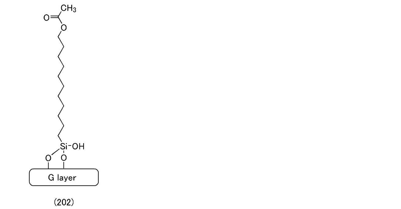
まず、フラスコに酸化グラフェン(株式会社仁科マテリアル製、製品名:Rap dGO(TQ-11)-1)0.41g、n-ブチルアミン5.6g(77mmol)を加えた。この混合液に窒素気流下で、超音波を5分照射し、さらに60℃で1時間撹拌した。撹拌後、この混合液を室温まで降温し、トルエン20mLを加え、超音波を5分照射した。この混合液を0℃に冷却後、11-アセトキシウンデシルトリクロロシラン11g(31mmol)を滴下し、60℃で5時間撹拌した。撹拌後、この混合液にトルエンを加えて洗浄し、ろ取物を吸引濾過により回収した。得られたろ取物をさらにエタノール、アセトンにより洗浄した。得られたろ取物を乾燥し、目的物の黒色粉末(試料1)を0.52g得た。下記に本合成スキーム(A)を示す。 First, 0.41 g of graphene oxide (manufactured by Nishina Material Co., Ltd., product name: Rap dGO (TQ-11) -1) and 5.6 g (77 mmol) of n-butylamine were added to the flask. The mixed solution was irradiated with ultrasonic waves for 5 minutes under a nitrogen stream, and further stirred at 60 ° C. for 1 hour. After stirring, the temperature of this mixture was lowered to room temperature, 20 mL of toluene was added, and ultrasonic waves were irradiated for 5 minutes. After cooling this mixed solution to 0 ° C., 11 g (31 mmol) of 11-acetoxyundecyltrichlorosilane was added dropwise, and the mixture was stirred at 60 ° C. for 5 hours. After stirring, toluene was added to this mixed solution for washing, and the filtrate was collected by suction filtration. The obtained filtrate was further washed with ethanol and acetone. The obtained filtrate was dried to obtain 0.52 g of the target black powder (Sample 1). The present synthesis scheme (A) is shown below.

<合成例2>
次に、実施の形態1で説明した本発明の一態様に係るグラフェン化合物の他の合成例について示す。すなわち、下記に示す構造式(203)で表される構造を有する酸化グラフェンの合成例について説明する。
<Synthesis example 2>
Next, another synthetic example of the graphene compound according to one aspect of the present invention described in the first embodiment will be shown. That is, an example of synthesizing graphene oxide having a structure represented by the structural formula (203) shown below will be described.

まず、フラスコに酸化グラフェン(株式会社仁科マテリアル製、製品名:Rap dGO(TQ-11)-1)0.61g、n-ブチルアミン8.4g(120mmol)を加えた。この混合液に窒素気流下で、超音波を5分照射し、さらに60℃で1時間撹拌した。撹拌後、この混合液を室温まで降温し、トルエン30mLを加え、超音波を5分照射した。この混合液を0℃に冷却後、2-アセトキシエチルトリクロロシラン10g(47mmol)を滴下し、60℃で5時間撹拌した。撹拌後、この混合液にトルエンを加えて洗浄し、ろ取物を吸引濾過により回収した。得られたろ取物をさらにエタノール、アセトンにより洗浄した。得られたろ取物を乾燥し、目的物の黒色粉末(試料2)を0.74g得た。下記に本合成スキーム(B)を示す。 First, 0.61 g of graphene oxide (manufactured by Nishina Material Co., Ltd., product name: Rap dGO (TQ-11) -1) and 8.4 g (120 mmol) of n-butylamine were added to the flask. The mixed solution was irradiated with ultrasonic waves for 5 minutes under a nitrogen stream, and further stirred at 60 ° C. for 1 hour. After stirring, the temperature of this mixture was lowered to room temperature, 30 mL of toluene was added, and ultrasonic waves were irradiated for 5 minutes. After cooling this mixed solution to 0 ° C., 10 g (47 mmol) of 2-acetoxyethyltrichlorosilane was added dropwise, and the mixture was stirred at 60 ° C. for 5 hours. After stirring, toluene was added to this mixed solution for washing, and the filtrate was collected by suction filtration. The obtained filtrate was further washed with ethanol and acetone. The obtained filtrate was dried to obtain 0.74 g of the target black powder (Sample 2). The present synthesis scheme (B) is shown below.

<合成例3>
次に、実施の形態1で説明した本発明の一態様に係るグラフェン化合物の他の合成例について示す。すなわち、下記に示す構造式(204)で表される構造を有する酸化グラフェンの合成例について説明する。
<Synthesis example 3>
Next, another synthetic example of the graphene compound according to one aspect of the present invention described in the first embodiment will be shown. That is, an example of synthesizing graphene oxide having a structure represented by the structural formula (204) shown below will be described.

まず、フラスコに酸化グラフェン(株式会社仁科マテリアル製、製品名:Rap dGO(TQ-11)-1)0.61g、n-ブチルアミン8.4g(120mmol)を加えた。この混合液に窒素気流下で、超音波を5分照射し、さらに60℃で1時間撹拌した。撹拌後、この混合液を室温まで降温し、トルエン30mLを加え、超音波を5分照射した。この混合液を0℃に冷却後、2-(カルボメトキシ)エチルトリクロロシラン10g(47mmol)を滴下し、60℃で5時間撹拌した。撹拌後、この混合液にトルエンを加えて洗浄し、ろ取物を吸引濾過により回収した。得られたろ取物をさらにエタノール、アセトンにより洗浄した。得られたろ取物を乾燥し、目的物の黒色粉末(試料3)を0.45g得た。下記に本合成スキーム(C)を示す。 First, 0.61 g of graphene oxide (manufactured by Nishina Material Co., Ltd., product name: Rap dGO (TQ-11) -1) and 8.4 g (120 mmol) of n-butylamine were added to the flask. The mixed solution was irradiated with ultrasonic waves for 5 minutes under a nitrogen stream, and further stirred at 60 ° C. for 1 hour. After stirring, the temperature of this mixture was lowered to room temperature, 30 mL of toluene was added, and ultrasonic waves were irradiated for 5 minutes. After cooling this mixed solution to 0 ° C., 10 g (47 mmol) of 2- (carbomethoxy) ethyltrichlorosilane was added dropwise, and the mixture was stirred at 60 ° C. for 5 hours. After stirring, toluene was added to this mixed solution for washing, and the filtrate was collected by suction filtration. The obtained filtrate was further washed with ethanol and acetone. The obtained filtrate was dried to obtain 0.45 g of the target black powder (Sample 3). The present synthesis scheme (C) is shown below.
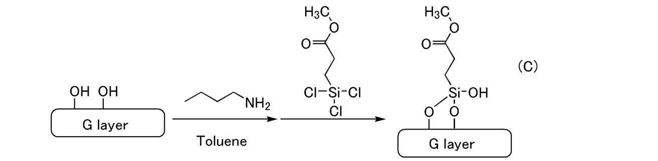
<FT-IR分析>
上述の合成例1乃至合成例3において、グラフェン化合物が化学修飾されたことを確認するため、フーリエ変換赤外分光(FT-IR:Fourier Transform Infrared Spectroscopy)測定を実施した。
<FT-IR analysis>
In the above-mentioned Synthesis Examples 1 to 3, Fourier transform infrared spectroscopy (FT-IR) measurement was performed to confirm that the graphene compound was chemically modified.
FT-IR測定は、上記合成例1で作製した化学修飾されたグラフェン化合物(試料1)、上記合成例2で作製した化学修飾されたグラフェン化合物(試料2)、上記合成例3で作製した化学修飾されたグラフェン化合物(試料3)、及び化学修飾されていない酸化グラフェン(比較用試料1)の4試料で実施した。 The FT-IR measurement was performed on the chemically modified graphene compound (sample 1) prepared in the above synthesis example 1, the chemically modified graphene compound (sample 2) prepared in the above synthesis example 2, and the chemistry prepared in the above synthesis example 3. It was carried out with 4 samples of a modified graphene compound (Sample 3) and a chemically unmodified graphene oxide (Comparative Sample 1).
FT-IR測定は、Thermo SCIENTIFIC社製Nicolet NEXUS 670を使用し、全反射測定法(ATR:Attenuated Total Reflection)で行った。測定範囲は600cm-1から4000cm-1まで、分解能は4.0cm-1、スキャン回数256回で行った。 The FT-IR measurement was performed by a total reflection measurement method (ATR: Attenuated Total Reflection) using a Nicolet NEXTUS 670 manufactured by Thermo SCIENTIFIC. The measurement range was 600 cm -1 to 4000 cm -1 , the resolution was 4.0 cm -1 , and the number of scans was 256.
なお、試料1乃至試料3は、上述の合成が完了した時点でフィルム状となったため、試料上からATRプリズムを押し当てて分析装置に設置した。比較用試料1は粉状であるが、同様に試料上からATRプリズムを押し当てて分析装置に設置した。 Since the samples 1 to 3 became a film when the above synthesis was completed, the ATR prism was pressed from the sample and installed in the analyzer. Although the comparative sample 1 is in the form of powder, the ATR prism was similarly pressed from above the sample and installed in the analyzer.
FT-IR測定結果を図9(A)乃至図9(D)に示す。図9(A)は試料1の、図9(B)は試料2の、図9(C)は試料3の、図9(D)は比較用試料1のFT-IRスペクトルである。図9(A)乃至図9(D)は、横軸に波数[cm-1]をとり、縦軸に透過率[%]をとる。
The FT-IR measurement results are shown in FIGS. 9 (A) to 9 (D). 9 (A) is the FT-IR spectrum of the sample 1, FIG. 9 (B) is the
図9(D)に示す化学修飾されていない酸化グラフェン(比較用試料1)は、C=O伸縮振動に帰属されると思われるピーク(1720cm-1付近)とC=C伸縮振動に帰属されると思われるピーク(1620cm-1付近)が観測された。すなわち、化学修飾していない状態の酸化グラフェンのFT-IRスペクトルを確認できた。 The non-chemically modified graphene oxide (comparative sample 1) shown in FIG. 9 (D) is attributed to the peak (around 1720 cm -1 ) and C = C stretching vibration, which are considered to be attributed to C = O stretching vibration. A peak (around 1620 cm -1 ) was observed. That is, the FT-IR spectrum of graphene oxide in the unchemically modified state could be confirmed.
一方で、図9(A)乃至図9(C)に示す化学修飾されたグラフェン化合物(試料1乃至試料3)は、C-H伸縮振動に帰属されると思われるピーク(2900cm-1付近)と、C=O伸縮振動に帰属されると思われるピーク(1750cm-1付近)が観測された。図9(D)に示す化学修飾していない状態の酸化グラフェン(比較用試料1)のスペクトルとは異なり、エステル結合及びアルキル基に起因すると考えられるピークを確認できた。 On the other hand, the chemically modified graphene compounds (Samples 1 to 3) shown in FIGS. 9 (A) to 9 (C) have a peak (around 2900 cm -1 ) that is considered to be attributed to CH stretching vibration. A peak (around 1750 cm -1 ) that seems to be attributed to C = O expansion and contraction vibration was observed. Unlike the spectrum of graphene oxide (comparative sample 1) in the unmodified state shown in FIG. 9 (D), a peak considered to be caused by an ester bond and an alkyl group could be confirmed.
したがって、試料1乃至試料3はエステル結合を有する基により化学修飾されていることが確認された。 Therefore, it was confirmed that Samples 1 to 3 were chemically modified with a group having an ester bond.
<XRD分析>
上述の合成例1乃至合成例3において、グラフェン化合物の層間距離を確認するため、XRD(X線回折)測定を実施した。
<XRD analysis>
In the above-mentioned Synthesis Examples 1 to 3, XRD (X-ray diffraction) measurement was carried out in order to confirm the interlayer distance of the graphene compound.
XRD測定は、上記合成例1で作製した化学修飾されたグラフェン化合物(試料1)、上記合成例2で作製した化学修飾されたグラフェン化合物(試料2)、上記合成例3で作製した化学修飾されたグラフェン化合物(試料3)、及び化学修飾されていない酸化グラフェン(比較用試料1)の4試料で実施した。 The XRD measurement was carried out by the chemically modified graphene compound (sample 1) prepared in the above synthesis example 1, the chemically modified graphene compound (sample 2) prepared in the above synthesis example 2, and the chemically modified graphene compound prepared in the above synthesis example 3. It was carried out with 4 samples of the graphene compound (Sample 3) and the chemically unmodified graphene oxide (Sample 1 for comparison).
XRD測定にはBruker AXS社製X線回折装置D8 ADVANCEを用いた。X線源として波長λ=0.15418nmのCuKα線を用い、スキャン範囲は2θ=2deg.から30deg.の範囲で測定した。 An X-ray diffractometer D8 ADVANCE manufactured by Bruker AXS was used for the XRD measurement. CuKα rays with a wavelength of λ = 0.15418 nm were used as the X-ray source, and the scan range was 2θ = 2deg. From 30 deg. It was measured in the range of.
XRD測定結果を図10(A)乃至図10(D)に示す。図10(A)は試料1の、図10(B)は試料2の、図10(C)は試料3の、図10(D)は比較用試料1のXRDスペクトルである。図10(A)乃至図10(D)は、横軸に回折角度2θ[deg.]をとり、縦軸に回折X線強度(任意単位)をとる。
The XRD measurement results are shown in FIGS. 10 (A) to 10 (D). 10 (A) is the XRD spectrum of the sample 1, FIG. 10 (B) is the XRD spectrum of the
いずれのサンプルも2θ=4deg.から10deg.の範囲にピークを確認できた。XRDのピーク角度と、ピーク角度から算出した平均層間距離を表1に示す。なお、平均層間距離は、2d×sinθ=λのBraggの式により算出した。ここで、θは回折ピークを得られるX線入射角度、dは面の間隔、λはXRD測定に使用したX線の波長を示す。 In each sample, 2θ = 4deg. From 10 deg. A peak could be confirmed in the range of. Table 1 shows the peak angle of XRD and the average interlayer distance calculated from the peak angle. The average interlayer distance was calculated by the Bragg equation of 2d × sin θ = λ. Here, θ is the X-ray incident angle at which the diffraction peak can be obtained, d is the surface spacing, and λ is the wavelength of the X-ray used for the XRD measurement.
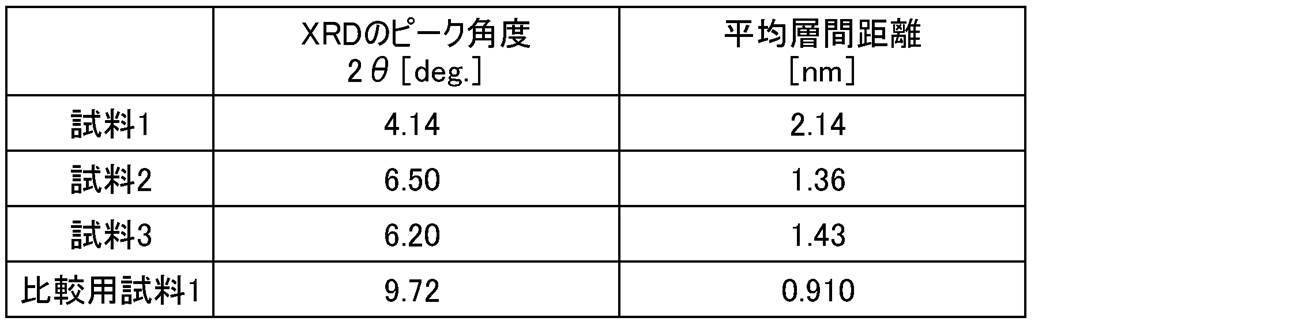
化学修飾されていない状態の酸化グラフェン(比較用試料1)と比較して、化学修飾された試料1乃至試料3は平均層間距離が大きくなっている。したがって、酸化グラフェンが化学修飾されたことにより、層間距離が大きくなったことが分かった。また、試料2及び試料3と比較して、官能基が長い試料1は平均層間距離が大きくなっている。酸化グラフェンに導入した官能基が長くなるほど、層間距離が大きくなることが分かった。層間距離が大きいほど、電子伝導性が低くなる為、正極と負極との間のショート(内部短絡)を防止するためには好適である。また、所望の電子伝導性となるように、官能基の長さを選択してもよい。
Compared with graphene oxide in the non-chemically modified state (comparative sample 1), the chemically modified samples 1 to 3 have a larger average interlayer distance. Therefore, it was found that the chemical modification of graphene oxide increased the interlayer distance. Further, as compared with the
したがって、試料1乃至試料3は化学修飾されたことにより、平均層間距離が大きくなったことが確認された。以上により、本発明の一態様に係る、エステル結合を有する基で化学修飾されたグラフェン化合物の合成を確認することができた。 Therefore, it was confirmed that the average interlayer distance was increased by chemically modifying Samples 1 to 3. From the above, it was possible to confirm the synthesis of the graphene compound chemically modified with the group having an ester bond according to one aspect of the present invention.
100 正極集電体
101 正極活物質層
102 負極集電体
103 負極活物質層
105 グラフェン化合物
107 セパレータ
109 外装体
110 リチウムイオン蓄電池
120 リチウムイオン蓄電池
200 情報処理装置
210 演算装置
220 入出力装置
230 表示部
250 蓄電装置
400 眼鏡型デバイス
400a フレーム
400b 表示部
401 ヘッドセット型デバイス
401a マイク部
401b フレキシブルパイプ
401c イヤフォン部
402 デバイス
402a 筐体
402b 蓄電装置
403 デバイス
403a 筐体
403b 蓄電装置
405 腕時計型デバイス
405a 表示部
405b ベルト部
406 ベルト型デバイス
406a ベルト部
406b ワイヤレス給電受電部
1700 曲面
1701 平面
1702 曲線
1703 曲率半径
1704 曲率中心
1800 曲率中心
1801 フィルム
1802 曲率半径
1803 フィルム
1804 曲率半径
1805 電池材料
7100 携帯表示装置
7101 筐体
7102 表示部
7103 操作ボタン
7104 蓄電装置
7400 携帯電話機
7401 筐体
7402 表示部
7403 操作ボタン
7404 外部接続ポート
7405 スピーカ
7406 マイク
7407 蓄電装置
7500 ストーブ
7501 蓄電装置
7511 モジュール
7511a 送風口
7511b 外部端子
7512 本体
7512a 開口部
7513 グリル
8021 充電装置
8022 ケーブル
8400 自動車
8401 ヘッドライト
8402 蓄電装置
8500 自動車
8600 スクータ
8601 サイドミラー
8602 蓄電装置
8603 方向指示灯
8604 座席下収納
100 Positive electrode
Claims (10)

(一般式(G1)において、G layerはグラフェン層を表し、R1は置換または無置換の炭素数1乃至炭素数20のアルキル基を表し、R2は水素、又は置換若しくは無置換の炭素数1乃至炭素数20のアルキル基を表す。) A graphene compound having a structure represented by the general formula (G1).
(In the general formula (G1), Grayer represents a graphene layer, R 1 represents a substituted or unsubstituted alkyl group having 1 to 20 carbon atoms, and R 2 represents hydrogen or a substituted or unsubstituted carbon number. Represents an alkyl group having 1 to 20 carbon atoms.)
前記一般式(G1)中、R1は置換または無置換の炭素数1乃至炭素数11のアルキル基であり、R2は置換または無置換の炭素数1乃至炭素数11のアルキル基であるグラフェン化合物。 In claim 1,
In the general formula (G1), R 1 is a substituted or unsubstituted alkyl group having 1 to 11 carbon atoms, and R 2 is a substituted or unsubstituted alkyl group having 1 to 11 carbon atoms. Compound.

(一般式(G2)において、G layerはグラフェン層を表し、R1は置換または無置換の炭素数1乃至炭素数20のアルキル基を表し、R2は水素、又は置換若しくは無置換の炭素数1乃至炭素数20のアルキル基を表す。) A graphene compound having a structure represented by the general formula (G2).
(In the general formula (G2), Grayer represents a graphene layer, R 1 represents a substituted or unsubstituted alkyl group having 1 to 20 carbon atoms, and R 2 represents hydrogen or a substituted or unsubstituted carbon number. Represents an alkyl group having 1 to 20 carbon atoms.)
前記一般式(G2)中、R1は置換または無置換の炭素数1乃至炭素数11のアルキル基であり、R2は置換または無置換の炭素数1乃至炭素数11のアルキル基であるグラフェン化合物。 In claim 3 ,
In the general formula (G2), R 1 is a substituted or unsubstituted alkyl group having 1 to 11 carbon atoms, and R 2 is a substituted or unsubstituted alkyl group having 1 to 11 carbon atoms. Compound.

(構造式(202)中において、G layerはグラフェン層を表す。) A graphene compound having a structure represented by the structural formula (202).
(In structural formula (202), Grayer represents a graphene layer.)
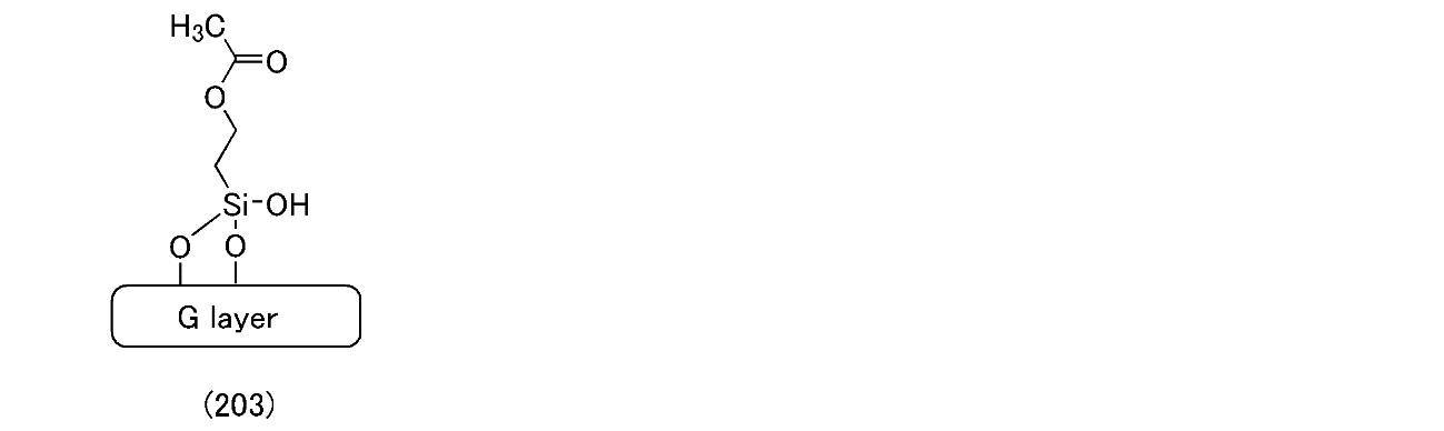
(構造式(203)中において、G layerはグラフェン層を表す。) A graphene compound having a structure represented by the structural formula (203).
(In structural formula (203), Grayer represents a graphene layer.)

(構造式(204)中において、G layerはグラフェン層を表す。) A graphene compound having a structure represented by the structural formula (204).
(In structural formula (204), Grayer represents a graphene layer.)
外装体と、正極集電体と、負極集電体と、を有する蓄電装置。 The electrolyte having the graphene compound according to any one of claims 1 to 7.
A power storage device having an exterior body, a positive electrode current collector, and a negative electrode current collector.
前記第1の混合液に、1つ以上のエステル基又はカルボキシル基を有するケイ素化合物を混合し撹拌して第2の混合液を形成し、
前記第2の混合液をろ過し、得られたろ取物を回収し、
前記ろ取物は、グラフェン化合物を含み、
前記ルイス塩基は、ブチルアミン、ペンチルアミン、ヘキシルアミン、ジエチルアミン、ジプロピルアミン、ジブチルアミン、トリエチルアミン、トリプロピルアミン、ピリジンのいずれか一以上であるグラフェン化合物の製造方法。 Graphene oxide and Lewis base are stirred to form a first mixed solution.
A silicon compound having one or more ester groups or carboxyl groups is mixed with the first mixed solution and stirred to form a second mixed solution.
The second mixed solution was filtered, and the obtained filtrate was collected.
The filter contains a graphene compound and contains
A method for producing a graphene compound, wherein the Lewis base is one or more of butylamine, pentylamine, hexylamine, diethylamine, dipropylamine, dibutylamine, triethylamine, tripropylamine, and pyridine.
前記第1の混合液に、ケイ素化合物を混合し撹拌して第2の混合液を形成し、
前記ケイ素化合物は11-アセトキシウンデシルトリクロロシラン、2-アセトキシエチルトリクロロシランまたは2-(カルボメトキシ)エチルトリクロロシランのいずれかであり、
前記第2の混合液をろ過し、得られたろ取物を回収し、
前記ろ取物は、グラフェン化合物を含むグラフェン化合物の製造方法。
Graphene oxide and butylamine are stirred to form a first mixed solution.
A silicon compound is mixed with the first mixed solution and stirred to form a second mixed solution.
The silicon compound is either 11-acetoxyundecyltrichlorosilane, 2-acetoxyethyltrichlorosilane or 2- (carbomethoxy) ethyltrichlorosilane.
The second mixed solution was filtered, and the obtained filtrate was collected.
The filter is a method for producing a graphene compound containing a graphene compound.
Applications Claiming Priority (2)
| Application Number | Priority Date | Filing Date | Title |
|---|---|---|---|
| JP2016138106 | 2016-07-13 | ||
| JP2016138106 | 2016-07-13 |
Publications (2)
| Publication Number | Publication Date |
|---|---|
| JP2018016539A JP2018016539A (en) | 2018-02-01 |
| JP7084113B2 true JP7084113B2 (en) | 2022-06-14 |
Family
ID=60941397
Family Applications (1)
| Application Number | Title | Priority Date | Filing Date |
|---|---|---|---|
| JP2017134414A Active JP7084113B2 (en) | 2016-07-13 | 2017-07-10 | Graphene compound, power storage device, and method for producing graphene compound |
Country Status (3)
| Country | Link |
|---|---|
| US (1) | US10529980B2 (en) |
| JP (1) | JP7084113B2 (en) |
| WO (1) | WO2018011675A1 (en) |
Families Citing this family (18)
| Publication number | Priority date | Publication date | Assignee | Title |
|---|---|---|---|---|
| WO2017149405A1 (en) * | 2016-03-02 | 2017-09-08 | Semiconductor Energy Laboratory Co., Ltd. | Graphene compound, method for forming graphene compound, and lithium-ion storage battery |
| CN110957479A (en) | 2016-07-05 | 2020-04-03 | 株式会社半导体能源研究所 | Positive active material |
| US12308421B2 (en) | 2016-09-12 | 2025-05-20 | Semiconductor Energy Laboratory Co., Ltd. | Electrode and power storage device comprising graphene compound |
| KR20190065324A (en) | 2016-10-12 | 2019-06-11 | 가부시키가이샤 한도오따이 에네루기 켄큐쇼 | Method for producing cathode active material particles and cathode active material particles |
| US10707524B2 (en) | 2016-10-19 | 2020-07-07 | Semiconductor Energy Laboratory Co., Ltd. | Graphene compound and manufacturing method thereof, electrolyte, and power storage device |
| CN118412521A (en) | 2017-05-12 | 2024-07-30 | 株式会社半导体能源研究所 | Positive electrode active material particles |
| KR20240023214A (en) | 2017-05-19 | 2024-02-20 | 가부시키가이샤 한도오따이 에네루기 켄큐쇼 | Positive electrode active material, method for manufacturing positive electrode active material, and secondary battery |
| CN110337744B (en) | 2017-06-26 | 2024-06-04 | 株式会社半导体能源研究所 | Method for producing positive electrode active material, and secondary battery |
| JPWO2019193450A1 (en) | 2018-04-05 | 2021-04-01 | 株式会社半導体エネルギー研究所 | Negative electrode active material, secondary battery, and electronic equipment |
| CN108574103B (en) * | 2018-04-28 | 2020-08-28 | 浙江天晨胶业股份有限公司 | Binder for lithium ion battery, preparation method, electrode material and electrode |
| US11225494B2 (en) * | 2018-07-13 | 2022-01-18 | Wilmar Trading Pte. Ltd. | Organosilane compounds and methods of making and using the same |
| CN111252764B (en) * | 2018-11-30 | 2023-04-07 | 中国科学院大连化学物理研究所 | Modified carbon material for lead-carbon battery, and preparation and application thereof |
| JP7449102B2 (en) * | 2019-02-27 | 2024-03-13 | キヤノン株式会社 | Modified graphene, method for producing modified graphene, modified graphene resin composite, modified graphene sheet, and modified graphene dispersion |
| EP3932861A4 (en) | 2019-03-27 | 2022-05-04 | Osaka University | METHOD FOR PRODUCTION OF MATERIAL WITH MODIFIED CARBON ALLOTROPE SURFACE, METHOD FOR PRODUCTION OF MATERIAL WITH CARBON ALLOTROPE SURFACE INTO WHICH A FUNCTIONAL GROUP IS INTRODUCED, METHOD FOR PRODUCTION OF GRID FOR CRYO-ELECTRONIC MICROSCOPY, ORGANIC MATERIAL AND GRID FOR CRYO-ELECTRONIC MICROSCOPY |
| KR102893452B1 (en) * | 2020-08-11 | 2025-12-02 | 주식회사 엘지에너지솔루션 | Positive electrode for a lithium secondary battery, method for preparing the same and lithium secondary battery comprising the positive electrode |
| CN113193180B (en) * | 2021-04-16 | 2023-05-26 | 西安交通大学 | Preparation method of silicon/functionalized graphene intercalation composite material with surface coupling activity |
| CN113773656B (en) * | 2021-09-07 | 2023-03-31 | 苏州鱼得水电气科技有限公司 | Compression-resistant noise-reducing asphalt cement and preparation method thereof |
| US20250014856A1 (en) * | 2021-10-07 | 2025-01-09 | Osaka University | Graphene grid, method for producing graphene grid, and method for analyzing structural analysis target substance |
Citations (1)
| Publication number | Priority date | Publication date | Assignee | Title |
|---|---|---|---|---|
| WO2011082064A1 (en) | 2009-12-29 | 2011-07-07 | Montclair State University | Chelating agent modified graphene oxides, methods of preparation and use |
Family Cites Families (21)
| Publication number | Priority date | Publication date | Assignee | Title |
|---|---|---|---|---|
| JPH05314965A (en) | 1992-05-06 | 1993-11-26 | Nippon Telegr & Teleph Corp <Ntt> | Battery positive electrode sheet, manufacture thereof and totally solid secondary battery |
| JPH05314995A (en) | 1992-05-07 | 1993-11-26 | Japan Energy Corp | Electrolyte composite body |
| JP4559587B2 (en) | 2000-05-08 | 2010-10-06 | 独立行政法人産業技術総合研究所 | Solid lithium polymer battery |
| JP4671589B2 (en) | 2003-07-15 | 2011-04-20 | 三星エスディアイ株式会社 | Electrolyte for lithium secondary battery and lithium secondary battery |
| US7491471B2 (en) | 2003-07-15 | 2009-02-17 | Samsung Sdi Co., Ltd. | Electrolyte for lithium secondary battery and lithium secondary battery comprising same |
| JP5613508B2 (en) | 2009-09-30 | 2014-10-22 | 株式会社半導体エネルギー研究所 | Redox capacitor |
| KR101944863B1 (en) | 2009-09-30 | 2019-02-01 | 가부시키가이샤 한도오따이 에네루기 켄큐쇼 | Electrochemical capacitor |
| WO2012077504A1 (en) | 2010-12-10 | 2012-06-14 | Semiconductor Energy Laboratory Co., Ltd. | Power storage device and method for manufacturing the power storage device |
| TW201226315A (en) | 2010-12-22 | 2012-07-01 | Montclair State University | Chelating agent modified graphene oxides, methods of preparation and use |
| JP6045162B2 (en) | 2011-03-25 | 2016-12-14 | 株式会社半導体エネルギー研究所 | Manufacturing method of secondary battery |
| KR101305438B1 (en) * | 2011-05-13 | 2013-09-06 | 현대자동차주식회사 | Adhesives for Bonding Polyurethane and Aluminium |
| CN102701191B (en) * | 2012-06-06 | 2013-11-20 | 渤海大学 | Preparation method of fluorosilane surface finished grapheme for supercapacitor |
| DK2864426T3 (en) | 2012-06-21 | 2022-06-07 | Tesla Nanocoatings Inc | ADJUSTABLE MATERIALS |
| US9290524B2 (en) * | 2013-03-15 | 2016-03-22 | Washington State University | Methods for producing functionalized graphenes |
| WO2016178117A1 (en) | 2015-05-06 | 2016-11-10 | Semiconductor Energy Laboratory Co., Ltd. | Secondary battery and electronic device |
| JP2016222526A (en) | 2015-05-29 | 2016-12-28 | 株式会社半導体エネルギー研究所 | Film formation method and element |
| US10784516B2 (en) | 2015-06-25 | 2020-09-22 | Semiconductor Energy Laboratory Co., Ltd. | Conductor, power storage device, electronic device, and method for forming conductor |
| US10686207B2 (en) | 2015-07-03 | 2020-06-16 | Semiconductor Energy Laboratory Co., Ltd. | Lithium-ion storage battery and electronic device |
| WO2017149405A1 (en) | 2016-03-02 | 2017-09-08 | Semiconductor Energy Laboratory Co., Ltd. | Graphene compound, method for forming graphene compound, and lithium-ion storage battery |
| US12308421B2 (en) | 2016-09-12 | 2025-05-20 | Semiconductor Energy Laboratory Co., Ltd. | Electrode and power storage device comprising graphene compound |
| KR102528223B1 (en) | 2016-12-09 | 2023-05-02 | 가부시키가이샤 한도오따이 에네루기 켄큐쇼 | Secondary battery and manufacturing method thereof |
-
2017
- 2017-07-06 WO PCT/IB2017/054062 patent/WO2018011675A1/en not_active Ceased
- 2017-07-10 JP JP2017134414A patent/JP7084113B2/en active Active
- 2017-07-11 US US15/646,626 patent/US10529980B2/en active Active
Patent Citations (1)
| Publication number | Priority date | Publication date | Assignee | Title |
|---|---|---|---|---|
| WO2011082064A1 (en) | 2009-12-29 | 2011-07-07 | Montclair State University | Chelating agent modified graphene oxides, methods of preparation and use |
Also Published As
| Publication number | Publication date |
|---|---|
| US10529980B2 (en) | 2020-01-07 |
| JP2018016539A (en) | 2018-02-01 |
| US20180019462A1 (en) | 2018-01-18 |
| WO2018011675A1 (en) | 2018-01-18 |
Similar Documents
| Publication | Publication Date | Title |
|---|---|---|
| JP7084113B2 (en) | Graphene compound, power storage device, and method for producing graphene compound | |
| JP6879642B2 (en) | Solid electrolyte, power storage device | |
| JP6957589B2 (en) | Power storage device and electronic equipment | |
| JP7793716B2 (en) | secondary battery | |
| JP7102099B2 (en) | Graphene compounds, graphene compound manufacturing methods, and lithium-ion storage batteries | |
| JP7661291B2 (en) | Electrode and power storage device | |
| JP6888920B2 (en) | Method of forming graphene compound sheet | |
| JP7081908B2 (en) | Lithium ion secondary battery | |
| JP2021064616A (en) | Manufacturing method for electrode | |
| JP7058986B2 (en) | Electronics | |
| JP7097690B2 (en) | Electrodes and storage batteries | |
| CN106169560B (en) | Electrode, power storage device, and electronic apparatus | |
| JP2020004738A (en) | Method for manufacturing active material | |
| KR20230006856A (en) | Electrodes, negative electrode active materials, secondary batteries, vehicles, and electronic devices, and manufacturing methods of negative electrode active materials | |
| CN113597410A (en) | Method for producing positive electrode active material | |
| JP7237221B2 (en) | lithium ion secondary battery | |
| JP2022033831A (en) | Graphene oxide |
Legal Events
| Date | Code | Title | Description |
|---|---|---|---|
| A621 | Written request for application examination |
Free format text: JAPANESE INTERMEDIATE CODE: A621 Effective date: 20200709 |
|
| A977 | Report on retrieval |
Free format text: JAPANESE INTERMEDIATE CODE: A971007 Effective date: 20210413 |
|
| A131 | Notification of reasons for refusal |
Free format text: JAPANESE INTERMEDIATE CODE: A131 Effective date: 20210511 |
|
| A521 | Request for written amendment filed |
Free format text: JAPANESE INTERMEDIATE CODE: A523 Effective date: 20210708 |
|
| A131 | Notification of reasons for refusal |
Free format text: JAPANESE INTERMEDIATE CODE: A131 Effective date: 20211124 |
|
| A521 | Request for written amendment filed |
Free format text: JAPANESE INTERMEDIATE CODE: A523 Effective date: 20220120 |
|
| TRDD | Decision of grant or rejection written | ||
| A01 | Written decision to grant a patent or to grant a registration (utility model) |
Free format text: JAPANESE INTERMEDIATE CODE: A01 Effective date: 20220510 |
|
| A61 | First payment of annual fees (during grant procedure) |
Free format text: JAPANESE INTERMEDIATE CODE: A61 Effective date: 20220602 |
|
| R150 | Certificate of patent or registration of utility model |
Ref document number: 7084113 Country of ref document: JP Free format text: JAPANESE INTERMEDIATE CODE: R150 |
|
| R250 | Receipt of annual fees |
Free format text: JAPANESE INTERMEDIATE CODE: R250 |