JP7063355B2 - Inductor bridges and electrical equipment - Google Patents
Inductor bridges and electrical equipment Download PDFInfo
- Publication number
- JP7063355B2 JP7063355B2 JP2020132793A JP2020132793A JP7063355B2 JP 7063355 B2 JP7063355 B2 JP 7063355B2 JP 2020132793 A JP2020132793 A JP 2020132793A JP 2020132793 A JP2020132793 A JP 2020132793A JP 7063355 B2 JP7063355 B2 JP 7063355B2
- Authority
- JP
- Japan
- Prior art keywords
- inductor
- connection portion
- conductor pattern
- conductor
- bridge
- Prior art date
- Legal status (The legal status is an assumption and is not a legal conclusion. Google has not performed a legal analysis and makes no representation as to the accuracy of the status listed.)
- Active
Links
Images


Classifications
-
- H—ELECTRICITY
- H01—ELECTRIC ELEMENTS
- H01F—MAGNETS; INDUCTANCES; TRANSFORMERS; SELECTION OF MATERIALS FOR THEIR MAGNETIC PROPERTIES
- H01F38/00—Adaptations of transformers or inductances for specific applications or functions
- H01F38/14—Inductive couplings
-
- H—ELECTRICITY
- H01—ELECTRIC ELEMENTS
- H01F—MAGNETS; INDUCTANCES; TRANSFORMERS; SELECTION OF MATERIALS FOR THEIR MAGNETIC PROPERTIES
- H01F1/00—Magnets or magnetic bodies characterised by the magnetic materials therefor; Selection of materials for their magnetic properties
- H01F1/01—Magnets or magnetic bodies characterised by the magnetic materials therefor; Selection of materials for their magnetic properties of inorganic materials
- H01F1/03—Magnets or magnetic bodies characterised by the magnetic materials therefor; Selection of materials for their magnetic properties of inorganic materials characterised by their coercivity
- H01F1/12—Magnets or magnetic bodies characterised by the magnetic materials therefor; Selection of materials for their magnetic properties of inorganic materials characterised by their coercivity of soft-magnetic materials
- H01F1/34—Magnets or magnetic bodies characterised by the magnetic materials therefor; Selection of materials for their magnetic properties of inorganic materials characterised by their coercivity of soft-magnetic materials non-metallic substances, e.g. ferrites
-
- H—ELECTRICITY
- H01—ELECTRIC ELEMENTS
- H01F—MAGNETS; INDUCTANCES; TRANSFORMERS; SELECTION OF MATERIALS FOR THEIR MAGNETIC PROPERTIES
- H01F27/00—Details of transformers or inductances, in general
- H01F27/24—Magnetic cores
- H01F27/245—Magnetic cores made from sheets, e.g. grain-oriented
-
- H—ELECTRICITY
- H01—ELECTRIC ELEMENTS
- H01F—MAGNETS; INDUCTANCES; TRANSFORMERS; SELECTION OF MATERIALS FOR THEIR MAGNETIC PROPERTIES
- H01F27/00—Details of transformers or inductances, in general
- H01F27/28—Coils; Windings; Conductive connections
- H01F27/2804—Printed windings
-
- H—ELECTRICITY
- H01—ELECTRIC ELEMENTS
- H01F—MAGNETS; INDUCTANCES; TRANSFORMERS; SELECTION OF MATERIALS FOR THEIR MAGNETIC PROPERTIES
- H01F27/00—Details of transformers or inductances, in general
- H01F27/28—Coils; Windings; Conductive connections
- H01F27/288—Shielding
- H01F27/2885—Shielding with shields or electrodes
-
- H—ELECTRICITY
- H01—ELECTRIC ELEMENTS
- H01F—MAGNETS; INDUCTANCES; TRANSFORMERS; SELECTION OF MATERIALS FOR THEIR MAGNETIC PROPERTIES
- H01F27/00—Details of transformers or inductances, in general
- H01F27/28—Coils; Windings; Conductive connections
- H01F27/29—Terminals; Tapping arrangements for signal inductances
-
- H—ELECTRICITY
- H01—ELECTRIC ELEMENTS
- H01F—MAGNETS; INDUCTANCES; TRANSFORMERS; SELECTION OF MATERIALS FOR THEIR MAGNETIC PROPERTIES
- H01F27/00—Details of transformers or inductances, in general
- H01F27/34—Special means for preventing or reducing unwanted electric or magnetic effects, e.g. no-load losses, reactive currents, harmonics, oscillations, leakage fields
- H01F27/36—Electric or magnetic shields or screens
- H01F27/363—Electric or magnetic shields or screens made of electrically conductive material
-
- H—ELECTRICITY
- H01—ELECTRIC ELEMENTS
- H01F—MAGNETS; INDUCTANCES; TRANSFORMERS; SELECTION OF MATERIALS FOR THEIR MAGNETIC PROPERTIES
- H01F27/00—Details of transformers or inductances, in general
- H01F27/40—Structural association with built-in electric component, e.g. fuse
-
- H—ELECTRICITY
- H01—ELECTRIC ELEMENTS
- H01Q—ANTENNAS, i.e. RADIO AERIALS
- H01Q1/00—Details of, or arrangements associated with, antennas
- H01Q1/36—Structural form of radiating elements, e.g. cone, spiral, umbrella; Particular materials used therewith
- H01Q1/38—Structural form of radiating elements, e.g. cone, spiral, umbrella; Particular materials used therewith formed by a conductive layer on an insulating support
-
- H—ELECTRICITY
- H01—ELECTRIC ELEMENTS
- H01Q—ANTENNAS, i.e. RADIO AERIALS
- H01Q1/00—Details of, or arrangements associated with, antennas
- H01Q1/50—Structural association of antennas with earthing switches, lead-in devices or lightning protectors
-
- H—ELECTRICITY
- H01—ELECTRIC ELEMENTS
- H01Q—ANTENNAS, i.e. RADIO AERIALS
- H01Q9/00—Electrically-short antennas having dimensions not more than twice the operating wavelength and consisting of conductive active radiating elements
- H01Q9/04—Resonant antennas
- H01Q9/30—Resonant antennas with feed to end of elongated active element, e.g. unipole
- H01Q9/42—Resonant antennas with feed to end of elongated active element, e.g. unipole with folded element, the folded parts being spaced apart a small fraction of the operating wavelength
-
- H—ELECTRICITY
- H03—ELECTRONIC CIRCUITRY
- H03H—IMPEDANCE NETWORKS, e.g. RESONANT CIRCUITS; RESONATORS
- H03H7/00—Multiple-port networks comprising only passive electrical elements as network components
- H03H7/01—Frequency selective two-port networks
- H03H7/0115—Frequency selective two-port networks comprising only inductors and capacitors
-
- H—ELECTRICITY
- H03—ELECTRONIC CIRCUITRY
- H03H—IMPEDANCE NETWORKS, e.g. RESONANT CIRCUITS; RESONATORS
- H03H7/00—Multiple-port networks comprising only passive electrical elements as network components
- H03H7/01—Frequency selective two-port networks
- H03H7/0123—Frequency selective two-port networks comprising distributed impedance elements together with lumped impedance elements
-
- H—ELECTRICITY
- H03—ELECTRONIC CIRCUITRY
- H03H—IMPEDANCE NETWORKS, e.g. RESONANT CIRCUITS; RESONATORS
- H03H7/00—Multiple-port networks comprising only passive electrical elements as network components
- H03H7/01—Frequency selective two-port networks
- H03H7/0138—Electrical filters or coupling circuits
-
- H—ELECTRICITY
- H03—ELECTRONIC CIRCUITRY
- H03H—IMPEDANCE NETWORKS, e.g. RESONANT CIRCUITS; RESONATORS
- H03H7/00—Multiple-port networks comprising only passive electrical elements as network components
- H03H7/01—Frequency selective two-port networks
- H03H7/17—Structural details of sub-circuits of frequency selective networks
- H03H7/1741—Comprising typical LC combinations, irrespective of presence and location of additional resistors
-
- H—ELECTRICITY
- H05—ELECTRIC TECHNIQUES NOT OTHERWISE PROVIDED FOR
- H05K—PRINTED CIRCUITS; CASINGS OR CONSTRUCTIONAL DETAILS OF ELECTRIC APPARATUS; MANUFACTURE OF ASSEMBLAGES OF ELECTRICAL COMPONENTS
- H05K1/00—Printed circuits
- H05K1/02—Details
- H05K1/0277—Bendability or stretchability details
- H05K1/028—Bending or folding regions of flexible printed circuits
-
- H—ELECTRICITY
- H05—ELECTRIC TECHNIQUES NOT OTHERWISE PROVIDED FOR
- H05K—PRINTED CIRCUITS; CASINGS OR CONSTRUCTIONAL DETAILS OF ELECTRIC APPARATUS; MANUFACTURE OF ASSEMBLAGES OF ELECTRICAL COMPONENTS
- H05K1/00—Printed circuits
- H05K1/02—Details
- H05K1/14—Structural association of two or more printed circuits
- H05K1/147—Structural association of two or more printed circuits at least one of the printed circuits being bent or folded, e.g. by using a flexible printed circuit
-
- H—ELECTRICITY
- H05—ELECTRIC TECHNIQUES NOT OTHERWISE PROVIDED FOR
- H05K—PRINTED CIRCUITS; CASINGS OR CONSTRUCTIONAL DETAILS OF ELECTRIC APPARATUS; MANUFACTURE OF ASSEMBLAGES OF ELECTRICAL COMPONENTS
- H05K1/00—Printed circuits
- H05K1/16—Printed circuits incorporating printed electric components, e.g. printed resistor, capacitor, inductor
- H05K1/165—Printed circuits incorporating printed electric components, e.g. printed resistor, capacitor, inductor incorporating printed inductors
-
- H—ELECTRICITY
- H01—ELECTRIC ELEMENTS
- H01F—MAGNETS; INDUCTANCES; TRANSFORMERS; SELECTION OF MATERIALS FOR THEIR MAGNETIC PROPERTIES
- H01F17/00—Fixed inductances of the signal type
- H01F17/0006—Printed inductances
- H01F2017/006—Printed inductances flexible printed inductors
-
- H—ELECTRICITY
- H01—ELECTRIC ELEMENTS
- H01F—MAGNETS; INDUCTANCES; TRANSFORMERS; SELECTION OF MATERIALS FOR THEIR MAGNETIC PROPERTIES
- H01F27/00—Details of transformers or inductances, in general
- H01F27/28—Coils; Windings; Conductive connections
- H01F27/2804—Printed windings
- H01F2027/2809—Printed windings on stacked layers
-
- H—ELECTRICITY
- H01—ELECTRIC ELEMENTS
- H01F—MAGNETS; INDUCTANCES; TRANSFORMERS; SELECTION OF MATERIALS FOR THEIR MAGNETIC PROPERTIES
- H01F27/00—Details of transformers or inductances, in general
- H01F27/28—Coils; Windings; Conductive connections
- H01F27/29—Terminals; Tapping arrangements for signal inductances
- H01F27/292—Surface mounted devices
- H01F2027/295—Surface mounted devices with flexible terminals
-
- H—ELECTRICITY
- H04—ELECTRIC COMMUNICATION TECHNIQUE
- H04M—TELEPHONIC COMMUNICATION
- H04M1/00—Substation equipment, e.g. for use by subscribers
- H04M1/02—Constructional features of telephone sets
- H04M1/0202—Portable telephone sets, e.g. cordless phones, mobile phones or bar type handsets
- H04M1/026—Details of the structure or mounting of specific components
- H04M1/0277—Details of the structure or mounting of specific components for a printed circuit board assembly
-
- H—ELECTRICITY
- H05—ELECTRIC TECHNIQUES NOT OTHERWISE PROVIDED FOR
- H05K—PRINTED CIRCUITS; CASINGS OR CONSTRUCTIONAL DETAILS OF ELECTRIC APPARATUS; MANUFACTURE OF ASSEMBLAGES OF ELECTRICAL COMPONENTS
- H05K1/00—Printed circuits
- H05K1/02—Details
- H05K1/0213—Electrical arrangements not otherwise provided for
- H05K1/0216—Reduction of cross-talk, noise or electromagnetic interference
- H05K1/0218—Reduction of cross-talk, noise or electromagnetic interference by printed shielding conductors, ground planes or power plane
- H05K1/0224—Patterned shielding planes, ground planes or power planes
- H05K1/0225—Single or multiple openings in a shielding, ground or power plane
-
- H—ELECTRICITY
- H05—ELECTRIC TECHNIQUES NOT OTHERWISE PROVIDED FOR
- H05K—PRINTED CIRCUITS; CASINGS OR CONSTRUCTIONAL DETAILS OF ELECTRIC APPARATUS; MANUFACTURE OF ASSEMBLAGES OF ELECTRICAL COMPONENTS
- H05K1/00—Printed circuits
- H05K1/02—Details
- H05K1/0213—Electrical arrangements not otherwise provided for
- H05K1/0216—Reduction of cross-talk, noise or electromagnetic interference
- H05K1/023—Reduction of cross-talk, noise or electromagnetic interference using auxiliary mounted passive components or auxiliary substances
- H05K1/0233—Filters, inductors or a magnetic substance
-
- H—ELECTRICITY
- H05—ELECTRIC TECHNIQUES NOT OTHERWISE PROVIDED FOR
- H05K—PRINTED CIRCUITS; CASINGS OR CONSTRUCTIONAL DETAILS OF ELECTRIC APPARATUS; MANUFACTURE OF ASSEMBLAGES OF ELECTRICAL COMPONENTS
- H05K1/00—Printed circuits
- H05K1/16—Printed circuits incorporating printed electric components, e.g. printed resistor, capacitor, inductor
- H05K1/162—Printed circuits incorporating printed electric components, e.g. printed resistor, capacitor, inductor incorporating printed capacitors
-
- H—ELECTRICITY
- H05—ELECTRIC TECHNIQUES NOT OTHERWISE PROVIDED FOR
- H05K—PRINTED CIRCUITS; CASINGS OR CONSTRUCTIONAL DETAILS OF ELECTRIC APPARATUS; MANUFACTURE OF ASSEMBLAGES OF ELECTRICAL COMPONENTS
- H05K2201/00—Indexing scheme relating to printed circuits covered by H05K1/00
- H05K2201/08—Magnetic details
- H05K2201/083—Magnetic materials
- H05K2201/086—Magnetic materials for inductive purposes, e.g. printed inductor with ferrite core
-
- H—ELECTRICITY
- H05—ELECTRIC TECHNIQUES NOT OTHERWISE PROVIDED FOR
- H05K—PRINTED CIRCUITS; CASINGS OR CONSTRUCTIONAL DETAILS OF ELECTRIC APPARATUS; MANUFACTURE OF ASSEMBLAGES OF ELECTRICAL COMPONENTS
- H05K2201/00—Indexing scheme relating to printed circuits covered by H05K1/00
- H05K2201/09—Shape and layout
- H05K2201/09209—Shape and layout details of conductors
- H05K2201/09218—Conductive traces
- H05K2201/09263—Meander
-
- H—ELECTRICITY
- H05—ELECTRIC TECHNIQUES NOT OTHERWISE PROVIDED FOR
- H05K—PRINTED CIRCUITS; CASINGS OR CONSTRUCTIONAL DETAILS OF ELECTRIC APPARATUS; MANUFACTURE OF ASSEMBLAGES OF ELECTRICAL COMPONENTS
- H05K2201/00—Indexing scheme relating to printed circuits covered by H05K1/00
- H05K2201/10—Details of components or other objects attached to or integrated in a printed circuit board
- H05K2201/10007—Types of components
- H05K2201/10098—Components for radio transmission, e.g. radio frequency identification [RFID] tag, printed or non-printed antennas
-
- H—ELECTRICITY
- H05—ELECTRIC TECHNIQUES NOT OTHERWISE PROVIDED FOR
- H05K—PRINTED CIRCUITS; CASINGS OR CONSTRUCTIONAL DETAILS OF ELECTRIC APPARATUS; MANUFACTURE OF ASSEMBLAGES OF ELECTRICAL COMPONENTS
- H05K2201/00—Indexing scheme relating to printed circuits covered by H05K1/00
- H05K2201/10—Details of components or other objects attached to or integrated in a printed circuit board
- H05K2201/10007—Types of components
- H05K2201/10189—Non-printed connector
-
- H—ELECTRICITY
- H05—ELECTRIC TECHNIQUES NOT OTHERWISE PROVIDED FOR
- H05K—PRINTED CIRCUITS; CASINGS OR CONSTRUCTIONAL DETAILS OF ELECTRIC APPARATUS; MANUFACTURE OF ASSEMBLAGES OF ELECTRICAL COMPONENTS
- H05K3/00—Apparatus or processes for manufacturing printed circuits
- H05K3/0058—Laminating printed circuit boards onto other substrates, e.g. metallic substrates
- H05K3/0061—Laminating printed circuit boards onto other substrates, e.g. metallic substrates onto a metallic substrate, e.g. a heat sink
Landscapes
- Engineering & Computer Science (AREA)
- Power Engineering (AREA)
- Microelectronics & Electronic Packaging (AREA)
- Chemical & Material Sciences (AREA)
- Dispersion Chemistry (AREA)
- Coils Or Transformers For Communication (AREA)
- Parts Printed On Printed Circuit Boards (AREA)
- Filters And Equalizers (AREA)
- Combinations Of Printed Boards (AREA)
- Details Of Aerials (AREA)
- Structure Of Printed Boards (AREA)
- Production Of Multi-Layered Print Wiring Board (AREA)
Description
本発明は、二つの回路間を接続する素子に関し、特にインダクタンス成分を有するインダクタブリッジおよびそれを備えた電子機器に関するものである。 The present invention relates to an element connecting two circuits, and particularly to an inductor bridge having an inductance component and an electronic device including the inductor bridge.
従来、携帯端末等の小型電子機器において、筐体内に複数の基板等の実装回路部材を備える場合に、例えば特許文献1に示されているように、可撓性を有するフラットケーブルで実装回路部材間が接続されている。
Conventionally, in a small electronic device such as a mobile terminal, when a plurality of mounting circuit members such as boards are provided in a housing, for example, as shown in
複数の基板を備え、基板同士をフラットケーブルで接続した従来の電子機器においては、必要に応じて基板に電子部品が実装されて、基板単位で回路が構成され、上記フラットケーブルは、単に基板同士を接続する配線として使用されている。 In a conventional electronic device having a plurality of boards and connecting the boards with a flat cable, electronic components are mounted on the boards as needed to form a circuit for each board. It is used as a wiring to connect.
このような、複数の基板等の実装回路部材を備えた電子機器においては、例えば回路に必要なインダクタを、基板にチップインダクタを実装することで実現するか、基板にインダクタの導体パターンを形成することで実現している。 In such an electronic device provided with a mounting circuit member such as a plurality of boards, for example, the inductor required for the circuit is realized by mounting a chip inductor on the board, or a conductor pattern of the inductor is formed on the board. It is realized by that.
しかし、チップインダクタを基板に実装する構造では、基板を薄くできず、電子機器全体の小型化を阻む一つの要因となる。一方、導体パターンでインダクタを形成する構造(以下「パターンインダクタ」)では、基板上の回路に対する占有面積が相対的に大きく、小型化を阻む一つの要因となる。 However, in the structure in which the chip inductor is mounted on the board, the board cannot be made thin, which is one of the factors that hinder the miniaturization of the entire electronic device. On the other hand, in a structure in which an inductor is formed by a conductor pattern (hereinafter referred to as “pattern inductor”), the area occupied by the circuit on the substrate is relatively large, which is one factor that hinders miniaturization.
勿論、チップインダクタ、パターンインダクタのいずれにおいても、形成する導体パターンを微細化すれば、小型化は可能であるが、そのことによりESR(等価直列抵抗)が大きくなったり、Q値が低下したりする問題が生じる。 Of course, in both chip inductors and pattern inductors, miniaturization is possible by miniaturizing the conductor pattern to be formed, but this may increase the ESR (equivalent series resistance) or decrease the Q value. Problems arise.
そこで、本発明の目的は、インダクタを有する電子回路を備えた電子機器の小型化を図ったインダクタブリッジおよび電子機器を提供することにある。 Therefore, an object of the present invention is to provide an inductor bridge and an electronic device for miniaturizing an electronic device provided with an electronic circuit having an inductor.
(1)本発明のインダクタブリッジは、アンテナを含む第1回路と第2回路との間をブリッジ接続するための素子であって、樹脂基材からなり、可撓性を有する平板状の素体と、前記素体に設けられ、第1回路に接続される第1接続部と、前記素体に設けられ、第2回路に接続される第2接続部と、前記素体の前記第1接続部と前記第2接続部との間に接続されたインダクタ部と、を備えることを特徴とする。また、インダクタブリッジは、前記第1回路と前記第2回路とは、高さ方向に異なる位置に設けられることを特徴とする。 (1) The inductor bridge of the present invention is an element for bridging between a first circuit including an antenna and a second circuit, and is made of a resin base material and has a flexible flat plate-shaped prime field. A first connection portion provided in the prime field and connected to the first circuit, a second connection portion provided in the prime field and connected to the second circuit, and the first connection of the prime field. It is characterized by including an inductor portion connected between the portion and the second connecting portion. Further, the inductor bridge is characterized in that the first circuit and the second circuit are provided at different positions in the height direction.
上記構成により、接続対象である基板等の実装回路部材にチップインダクタやパターンインダクタを設けることなく、回路中にインダクタを設けることができるので、小型化が図れる。また、チップインダクタを基板等の実装回路部材に実装する工数が削減されるので、低コスト化が図れる。 With the above configuration, it is possible to provide an inductor in the circuit without providing a chip inductor or a pattern inductor in a mounting circuit member such as a board to be connected, so that miniaturization can be achieved. Further, since the man-hours for mounting the chip inductor on the mounting circuit member such as a board are reduced, the cost can be reduced.
(2)前記第1接続部および第2接続部は機械的接触により電気的に接続されるものであることが好ましい。これにより、回路間を電気的・機械的に接続する接続具として用いることができる。 (2) It is preferable that the first connection portion and the second connection portion are electrically connected by mechanical contact. As a result, it can be used as a connector for electrically and mechanically connecting circuits.
(3)前記素体は樹脂基材の積層体であり、前記樹脂基材の材質は液晶ポリマー(LCP)であることが好ましい。これにより、低誘電率特性が活かされて浮遊容量が少なく、より高周波帯域までインダクタとして用いることができる。 (3) The prime field is preferably a laminated body of a resin base material, and the material of the resin base material is preferably a liquid crystal polymer (LCP). As a result, the low dielectric constant characteristic is utilized, the stray capacitance is small, and the inductor can be used up to a higher frequency band.
(4)前記インダクタ部は、例えば前記素体の主面に垂直方向にコイル軸が向くスパイラル状の導体パターンを備える。これにより、少ない層数で大きなインダクタンスを得ることができ、必要なインダクタンスを得るに要する平面サイズが縮小化できる。 (4) The inductor portion includes, for example, a spiral conductor pattern in which the coil axis faces in a direction perpendicular to the main surface of the prime field. As a result, a large inductance can be obtained with a small number of layers, and the plane size required to obtain the required inductance can be reduced.
(5)前記素体が長手方向を有する場合に、前記インダクタ部は、例えば互いに隣接する線路のそれぞれが前記素体の長手方向に延びるミアンダライン状の導体パターンを備える。これにより、長手方向の剛性を高められる。また、インダクタ部の位置以外での屈曲が容易となる。 (5) When the prime field has a longitudinal direction, the inductor portion includes, for example, a meander line-shaped conductor pattern in which lines adjacent to each other extend in the longitudinal direction of the prime field. As a result, the rigidity in the longitudinal direction can be increased. In addition, bending other than the position of the inductor portion becomes easy.
(6)前記素体が短手方向を有する場合に、前記インダクタ部は、例えば互いに隣接する線路のそれぞれが前記素体の短手方向に延びるミアンダライン状の導体パターンである。これにより、長手方向の全体の柔軟性を高められる。また、素体の屈曲量に対するインダクタンスの変化量が抑制できる。 (6) When the prime field has a lateral direction, the inductor portion is, for example, a meander line-shaped conductor pattern in which lines adjacent to each other extend in the lateral direction of the prime field. This increases the overall flexibility in the longitudinal direction. In addition, the amount of change in inductance with respect to the amount of bending of the prime field can be suppressed.
(7)前記導体パターンは、例えば複数の層に亘って形成され、隣接する層に形成された導体パターンは平面視で重ならないように配置されている。これにより、層数の増加に伴うインダクタンスの増大の割には浮遊容量の増加が少なく、より高周波帯域までインダクタとして用いることができる。 (7) The conductor pattern is formed, for example, over a plurality of layers, and the conductor patterns formed on the adjacent layers are arranged so as not to overlap in a plan view. As a result, the increase in stray capacitance is small for the increase in inductance due to the increase in the number of layers, and it can be used as an inductor up to a higher frequency band.
(8)前記導体パターンは、例えば複数の層に亘って形成され、複数の導体パターンは並列接続されている。これにより、等価直列抵抗を低減できる。 (8) The conductor pattern is formed, for example, over a plurality of layers, and the plurality of conductor patterns are connected in parallel. As a result, the equivalent series resistance can be reduced.
(9)前記インダクタ部は、例えば前記素体の主面に平行方向にコイル軸が向くヘリカル状の導体パターンである。これにより、導体が隣接しても、その導体に渦電流が生じ難く、周囲環境によるインダクタンスの変動が抑制される。 (9) The inductor portion is, for example, a helical conductor pattern in which the coil axis faces in a direction parallel to the main surface of the prime field. As a result, even if conductors are adjacent to each other, eddy currents are unlikely to occur in the conductors, and fluctuations in inductance due to the surrounding environment are suppressed.
(10)前記素体内の前記導体パターンの近傍に磁性体(コア)が配置されていることが好ましい。これにより、より小型化される。 (10) It is preferable that a magnetic material (core) is arranged in the vicinity of the conductor pattern in the element body. As a result, the size is further reduced.
(11)前記第1接続部は前記素体の第1端部に設けられ、前記第2接続部は前記素体の第2端部に設けられ、前記素体は前記第1端部から前記第2端部までの途中に屈曲部を有することが好ましい。これにより、屈曲した状態で二つの回路間を接続することができ、電子機器の筐体内の限られたスペースに収め易くなる。 (11) The first connection portion is provided at the first end portion of the prime field, the second connection portion is provided at the second end portion of the prime field, and the prime field is provided from the first end portion to the above. It is preferable to have a bent portion on the way to the second end portion. As a result, the two circuits can be connected in a bent state, and it becomes easy to fit in the limited space inside the housing of the electronic device.
(12)前記屈曲部はライン(屈曲線)に沿うように屈曲される部分であり、且つ前記インダクタ部の形成範囲内にあり、前記インダクタ部は、長軸が前記ラインに対して非垂直な楕円形状に形成されていることが好ましい。これにより、インダクタ部を構成する導体パターンの断線が生じにくくなる。 (12) The bent portion is a portion that is bent along a line (bending line) and is within the formation range of the inductor portion, and the long axis of the inductor portion is not perpendicular to the line. It is preferably formed in an elliptical shape. As a result, disconnection of the conductor pattern constituting the inductor portion is less likely to occur.
(13)上記(11)において、屈曲部は前記インダクタ部の中心を通るライン以外の位置であることが好ましい。これにより、柔軟性の高い位置での屈曲が容易となり、インダクタ部への応力が抑制され、インダクタとしての特性も維持し易くなる。 (13) In the above (11), it is preferable that the bent portion is at a position other than the line passing through the center of the inductor portion. This facilitates bending at a highly flexible position, suppresses stress on the inductor portion, and facilitates maintenance of the characteristics of the inductor.
(14)上記(13)において、屈曲部に層間接続導体(ビア)が形成されていることが好ましい。 (14) In the above (13), it is preferable that an interlayer connecting conductor (via) is formed at the bent portion.
(15)前記素体に、前記インダクタ部を層方向に挟む位置に、シールド導体パターンが形成されていることが好ましい。これにより、インダクタ部が電磁シールドされて、安定した特性が得られる。 (15) It is preferable that the shield conductor pattern is formed on the prime field at a position where the inductor portion is sandwiched in the layer direction. As a result, the inductor portion is electromagnetically shielded, and stable characteristics can be obtained.
(16)前記インダクタ部は、前記素体の主面に垂直方向にコイル軸が向き、且つ複数の層に亘ってヘリカル状に形成された導体パターンを備え、これらの導体パターンは層間で対向する位置に形成されていて、これらの複数の導体パターンのうち、前記第1接続部および前記第2接続部に経路上近い(最外層の)導体パターンの線幅は他の層の導体パターンの線幅より細いことが好ましい。この構成により、寄生容量が抑制されて、自己共振周波数が高くなり、通過帯域幅が広くなる。 (16) The inductor portion includes a conductor pattern in which the coil axis faces in a direction perpendicular to the main surface of the prime field and is formed in a helical shape over a plurality of layers, and these conductor patterns face each other between layers. Of these plurality of conductor patterns formed at positions, the line width of the conductor pattern (outermost layer) close to the first connection portion and the second connection portion on the path is the line of the conductor pattern of the other layer. It is preferably thinner than the width. This configuration suppresses parasitic capacitance, increases the self-resonant frequency, and widens the passband.
(17)前記インダクタ部は、前記素体の主面に垂直方向にコイル軸が向き、且つ複数の層に亘ってヘリカル状に形成された導体パターンを備え、これらの導体パターンは層間で対向する位置に形成されていて、これらの複数の導体パターンのうち、前記第1接続部および前記第2接続部に経路上近い(最外層の)導体パターンと、この導体パターンに対する隣接層の導体パターンとの間隔は、他の隣接層における導体パターン間の間隔より広いことが好ましい。この構成により、寄生容量が抑制されて、自己共振周波数が高くなり、通過帯域幅が広くなる。 (17) The inductor portion includes a conductor pattern in which the coil axis faces in a direction perpendicular to the main surface of the prime field and is formed in a helical shape over a plurality of layers, and these conductor patterns face each other between layers. Of these plurality of conductor patterns formed at positions, a conductor pattern (outermost layer) close to the first connection portion and the second connection portion on the path, and a conductor pattern of an adjacent layer to the conductor pattern. The spacing between the conductors is preferably wider than the spacing between the conductor patterns in the other adjacent layers. This configuration suppresses parasitic capacitance, increases the self-resonant frequency, and widens the passband.
(18)本発明の電子機器は、上記(1)~(17)のいずれかに記載のインダクタブリッジ、第1回路および第2回路を備え、第1回路と第2回路とが前記インダクタブリッジを介して接続されていることを特徴とする。 (18) The electronic device of the present invention includes the inductor bridge, the first circuit and the second circuit according to any one of (1) to (17) above, and the first circuit and the second circuit form the inductor bridge. It is characterized by being connected via.
(19)上記(18)において、例えば第1回路を構成する第1実装回路部材と、第2回路を構成する第2実装回路部材とは高さ方向に異なる位置に設けられ、インダクタブリッジは、屈曲状態で第1接続部が第1実装回路部材に接続され、第2接続部が第2実装回路部材に接続されている。 (19) In the above (18), for example, the first mounting circuit member constituting the first circuit and the second mounting circuit member constituting the second circuit are provided at different positions in the height direction, and the inductor bridge is provided. In the bent state, the first connecting portion is connected to the first mounting circuit member, and the second connecting portion is connected to the second mounting circuit member.
(20)本発明の電子機器は、上記(4)に記載のインダクタブリッジ、第1回路および第2回路を備え、第1回路を構成する第1実装回路部材と、第2回路を構成する第2実装回路部材とは高さ方向に異なる位置に設けられ、第2実装回路部材にはグランド導体パターンが形成されていて、インダクタブリッジは、屈曲状態で前記インダクタ部のコイル軸が第2実装回路部材の面に対し非垂直となる状態で第1実装回路部材と第2実装回路部材との間に接続されていることを特徴とする。この構成により、インダクタ部とグランド導体との不要結合が抑制され、グランド導体に生じる渦電流が抑制される。 (20) The electronic device of the present invention includes the inductor bridge, the first circuit, and the second circuit according to the above (4), the first mounting circuit member constituting the first circuit, and the second circuit constituting the second circuit. A ground conductor pattern is formed on the second mounting circuit member, which is provided at a position different from that of the two mounting circuit members in the height direction. It is characterized in that it is connected between the first mounting circuit member and the second mounting circuit member in a state of being non-vertical to the surface of the member. With this configuration, unnecessary coupling between the inductor portion and the ground conductor is suppressed, and the eddy current generated in the ground conductor is suppressed.
(21)本発明の電子機器は、上記(1)~(17)のいずれかのインダクタブリッジと、前記第1接続部が導通する面状導体(グランド電極)が形成された実装回路部材(基板)とを備え、前記インダクタブリッジは、前記第1接続部に繋がる第1配線パターン、および前記第2接続部に繋がる第2配線パターンを備え、前記第2配線パターンおよび前記インダクタ部は前記第1配線パターンに比べて前記面状導体より離れた層に形成されていることが好ましい。 (21) The electronic device of the present invention is a mounting circuit member (board) in which an inductor bridge according to any one of (1) to (17) above and a planar conductor (ground electrode) through which the first connection portion conducts are formed. The inductor bridge includes a first wiring pattern connected to the first connection portion and a second wiring pattern connected to the second connection portion, and the second wiring pattern and the inductor portion are the first. It is preferably formed in a layer separated from the planar conductor as compared with the wiring pattern.
(22)本発明の電子機器は、上記(1)~(17)のいずれかのインダクタブリッジと、前記第1接続部が導通するアンテナ素子パターンが形成されたアンテナとを備え、前記インダクタブリッジは、前記第1接続部に繋がる第1配線パターン、および前記第2接続部に繋がる第2配線パターンを備え、前記第2配線パターンは前記第1配線パターンに比べて前記アンテナ素子パターンより離れた層に形成されていることが好ましい。 (22) The electronic device of the present invention includes the inductor bridge according to any one of (1) to (17) above and an antenna having an antenna element pattern in which the first connection portion conducts. The second wiring pattern includes a first wiring pattern connected to the first connection portion and a second wiring pattern connected to the second connection portion, and the second wiring pattern is a layer separated from the antenna element pattern as compared with the first wiring pattern. It is preferable that it is formed in.
(23)本発明の電子機器は、上記(1)~(17)のいずれかのインダクタブリッジと、前記第1接続部が導通するアンテナ素子パターンが形成されたアンテナと、前記第2接続部が導通する面状導体とを備え、前記インダクタブリッジは、前記第1接続部に繋がる第1配線パターン、および前記第2接続部に繋がる第2配線パターンを備え、前記第1配線パターンは前記第2配線パターンに比べて前記面状導体より離れた層に形成されていることが好ましい。 (23) In the electronic device of the present invention, the inductor bridge according to any one of (1) to (17) above, an antenna having an antenna element pattern in which the first connection portion conducts, and the second connection portion are used. The inductor bridge includes a conductive planar conductor, the inductor bridge includes a first wiring pattern connected to the first connection portion, and a second wiring pattern connected to the second connection portion, and the first wiring pattern is the second wiring pattern. It is preferable that the layer is formed in a layer farther from the planar conductor as compared with the wiring pattern.
(24)本発明の電子機器は、上記(1)~(17)のいずれかのインダクタブリッジと、前記第1接続部が導通するアンテナ素子パターンが形成されたアンテナと、前記インダクタブリッジを間にして前記アンテナの反対側に配置された金属部材とを備え、前記インダクタブリッジは、前記第1接続部に繋がる第1配線パターン、および前記第2接続部に繋がる第2配線パターンを備え、前記第1配線パターンは前記第2配線パターンに比べて前記金属部材から離れた層に形成されていることが好ましい。 (24) In the electronic device of the present invention, the inductor bridge according to any one of (1) to (17) above, an antenna on which an antenna element pattern in which the first connection portion conducts is formed, and the inductor bridge are interposed. The inductor bridge includes a first wiring pattern connected to the first connection portion and a second wiring pattern connected to the second connection portion, and is provided with a metal member arranged on the opposite side of the antenna. It is preferable that the 1 wiring pattern is formed in a layer separated from the metal member as compared with the 2nd wiring pattern.
(25)本発明の電子機器は、上記(1)~(17)のいずれかのインダクタブリッジと、面状導体(バッテリーなど)とを備え、前記インダクタ部は、前記素体の主面に垂直方向にコイル軸が向き、且つ複数の層に亘ってスパイラル状に形成された導体パターンを備え、これらの導体パターンのうち、巻回数の多い導体パターンが形成された層が前記面状導体より離れた層に配置されていることが好ましい。 (25) The electronic device of the present invention includes the inductor bridge according to any one of (1) to (17) above and a planar conductor (battery or the like), and the inductor portion is perpendicular to the main surface of the element body. It has a conductor pattern in which the coil axis is oriented in the direction and is formed in a spiral shape over a plurality of layers. Among these conductor patterns, the layer in which the conductor pattern having a large number of turns is formed is separated from the planar conductor. It is preferably arranged in a layer.
(26)本発明の電子機器は、上記(1)~(17)のいずれかのインダクタブリッジを備え、前記インダクタ部は、前記素体の主面に垂直方向にコイル軸が向き、且つ複数の層に亘ってスパイラル状に形成された導体パターンを備え、これらの導体パターンは層間で対向する位置に形成されていることが好ましい。 (26) The electronic device of the present invention includes the inductor bridge according to any one of (1) to (17) above, and the inductor portion has a plurality of coil axes oriented in a direction perpendicular to the main surface of the prime field. It is preferable that the conductor patterns are spirally formed over the layers, and these conductor patterns are formed at positions facing each other between the layers.
(27)本発明の電子機器は、上記(1)~(17)のいずれかのインダクタブリッジと、面状導体(金属体)とを備え、前記インダクタ部は、前記素体の主面に垂直方向にコイル軸が向き、且つ複数の層に亘ってスパイラル状に形成された導体パターンを備え、これらの導体パターンは、前記面状導体との間で容量が生じる位置に形成されていることが好ましい。 (27) The electronic device of the present invention includes the inductor bridge according to any one of (1) to (17) above and a planar conductor (metal body), and the inductor portion is perpendicular to the main surface of the prime field. The coil axis is oriented in the direction, and the conductor pattern is formed in a spiral shape over a plurality of layers, and these conductor patterns are formed at a position where a capacitance is generated between the conductor pattern and the planar conductor. preferable.
(28)上記(27)において、前記容量と前記インダクタ部とでローパスフィルタが構成されていることが好ましい。 (28) In the above (27), it is preferable that the low-pass filter is configured by the capacitance and the inductor portion.
本発明によれば、接続対象である基板等の実装回路部材にチップインダクタやパターンインダクタを設けることなく、回路中にインダクタを設けることができるので、小型化が図れる。また、チップインダクタを基板等の実装回路部材に実装する工数が削減されるので、低コスト化が図れる。 According to the present invention, since an inductor can be provided in a circuit without providing a chip inductor or a pattern inductor in a mounting circuit member such as a board to be connected, miniaturization can be achieved. Further, since the man-hours for mounting the chip inductor on the mounting circuit member such as a board are reduced, the cost can be reduced.
以降、図を参照して幾つかの具体的な例を挙げて、本発明を実施するための複数の形態を示す。各図中には同一箇所に同一符号を付している。各実施形態は例示であり、異なる実施形態で示した構成の部分的な置換または組み合わせが可能であることは言うまでもない。 Hereinafter, a plurality of embodiments for carrying out the present invention will be shown with reference to the drawings with reference to some specific examples. The same reference numerals are given to the same parts in each figure. It goes without saying that each embodiment is exemplary and the configurations shown in the different embodiments can be partially replaced or combined.
《第1の実施形態》
図1(A)は第1の実施形態に係るインダクタブリッジの外観斜視図、図1(B)はその分解斜視図である。このインダクタブリッジ101Aは第1回路と第2回路との間をブリッジ接続するための素子である。図1(A)に表れているように、このインダクタブリッジ101Aは、可撓性を有する平板状の素体10、第1コネクタ51および第2コネクタ52を備えている。素体10の内部には、後に述べるインダクタ部が構成されている。第1コネクタ51は、素体10の第1端部に設けられ、第1回路に機械的接触により接続される。第2コネクタ52は、素体10の第2端部に設けられ、第2回路に機械的接触により接続される。第1コネクタ51は本発明に係る「第1接続部」に相当し、第2コネクタ52は本発明に係る「第2接続部」に相当する。
<< First Embodiment >>
FIG. 1A is an external perspective view of the inductor bridge according to the first embodiment, and FIG. 1B is an exploded perspective view thereof. The
図1(B)に表れているように、上記素体10は液晶ポリマー(LCP)の樹脂基材11,12,13が積層されることで構成される。樹脂基材12には導体パターン31によるインダクタ部30が構成されている。導体パターン31は、樹脂基材12の面に垂直方向(素体10の主面に垂直方向)にコイル軸が向くスパイラル状の導体パターンである。
As shown in FIG. 1 (B), the
樹脂基材12には配線パターン21,22が形成されていて、樹脂基材13には配線パターン23が形成されている。配線パターン21の第1端はインダクタ部の導体パターン31の外周端につながり、導体パターン31の内周端はビア導体(層間接続導体)を介して配線パターン23の第1端につながり、配線パターン23の第2端はビア導体を介して配線パターン22の第1端につながっている。
樹脂基材11にはコネクタ51,52を実装するためのコネクタ実装電極41,42が形成されている。これらコネクタ実装電極41,42はビア導体を介して配線パターン21,22の第2端にそれぞれ接続されている。
The
樹脂基材11の上面にはレジスト層61が形成されていて、樹脂基材13の下面にはレジスト層62が形成されている。なお、レジスト層62は必須ではなく、形成しなくてもよい。
A resist
上記インダクタブリッジ101Aの製造方法は次のとおりである。
The manufacturing method of the
(1)先ず樹脂基材と金属箔(例えば銅箔)とをラミネートし、その金属箔をフォトリソグラフィでパターンニングすることで、配線パターン21,22,23、導体パターン31、コネクタ実装電極41,42を形成する。また、樹脂基材11,12にビア導体を形成する。ビア導体は、レーザー等で貫通孔を設けた後、銅、銀、錫などを含む導電性ペーストを配設し、後の加熱・加圧工程で硬化させることによって設けられる。
(1) First, a resin base material and a metal foil (for example, copper foil) are laminated, and the metal foil is patterned by photolithography to form
(2)樹脂基材11,12,13を積層し、加熱・加圧することで積層体を構成する。
(2) The
(3)積層体の両面にレジスト層61,62をそれぞれ印刷形成する。
(3) Resist
(4)コネクタ51,52をはんだ付けする。
(4) Solder the
(5)集合基板を分断することで、個別のインダクタブリッジ101Aを得る。 (5) Individual inductor bridges 101A are obtained by dividing the assembly board.
図2(A)は第1の実施形態に係る別のインダクタブリッジの外観斜視図、図2(B)はその分解斜視図である。このインダクタブリッジ101Bは、素体10に対する第1コネクタ51と第2コネクタ52との取り付け面が異なっている。
FIG. 2A is an external perspective view of another inductor bridge according to the first embodiment, and FIG. 2B is an exploded perspective view thereof. The
図2(B)に表れているように、コネクタ実装電極42は樹脂基材13の下面に形成されている。レジスト層61,62はコネクタ実装電極41,42の位置に応じたパターンに形成されている。その他の構成は図1に示した例と同じである。
As shown in FIG. 2B, the
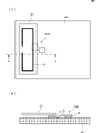
図3(A)は、上記インダクタブリッジ101Bを用いてマザー基板201とアンテナ基板301とを接続した状態での平面図、図3(B)は、図3(A)のA-A部分の断面図である。なお、ここでは、アンテナ基板301が第1実装回路部材に相当し、マザー基板201が第2実装回路部材に相当する。また、図3(B)に示すように、アンテナ基板301とマザー基板201とは高さ方向に異なる位置に設けられている。
FIG. 3A is a plan view in a state where the
アンテナ基板301にはアンテナ素子パターン91が形成されている。このアンテナ素子パターン91の給電点、または給電点から引き出した箇所にインダクタブリッジ101Bの第1コネクタ51が接続される。インダクタブリッジ101Bの第2コネクタ52はマザー基板201の上面に形成されている接続部に接続される。
The
図4(A)は、上記インダクタブリッジ101Bとアンテナ基板301とを備えた高周波回路のブロック図、図4(B)はその等価回路図である。インダクタL1はインダクタブリッジ101Bに形成されたインダクタである。図4(A)に示すように、アンテナANTとRFICとの間にインダクタL1が接続されている。すなわち、図4(B)に示すように、アンテナ素子パターン91の給電部にインダクタL1が直列に挿入されている。このインダクタL1によって、給電回路(RFIC)とアンテナとのインピーダンスマッチングおよびアンテナの周波数特性が定められる。
FIG. 4A is a block diagram of a high frequency circuit including the
図5はアンテナ基板301とインダクタブリッジ101Cとの接続部の構造の例を示す図である。インダクタブリッジ101Cのコネクタ以外の構成は、既に示したインダクタブリッジ101A,101Bと同じである。アンテナ素子パターン91の給電点に孔H1が形成されている。インダクタブリッジ101Cの第1端部には電極(第1接続部)および孔H3が形成されている。このインダクタブリッジ側の孔H3を介してネジを孔H1にネジ留めすることにより、機械的・電気的に接続する。
FIG. 5 is a diagram showing an example of the structure of the connection portion between the
図6(A)はインダクタブリッジの別の適用例を示すブロック図、図6(B)はその等価回路図である。この例は、逆F型アンテナにおけるグランド接続点とグランドとの間にインダクタを挿入したアンテナを構成する例である。 FIG. 6A is a block diagram showing another application example of the inductor bridge, and FIG. 6B is an equivalent circuit diagram thereof. This example is an example of configuring an antenna in which an inductor is inserted between the ground connection point and the ground in an inverted-F antenna.
図6(A)、図6(B)において、インダクタL2はインダクタブリッジ102に形成されたインダクタである。アンテナANTとグランドとの間にインダクタL2が接続されて、逆F型アンテナが構成されている。すなわち、図6(B)に示すように、アンテナ素子パターン91の一端とグランドとの間にインダクタL2が接続されていて、アンテナ素子パターン91のうちインダクタL2の近傍に給電回路(RFIC)が接続されている。
In FIGS. 6A and 6B, the inductor L2 is an inductor formed on the
図7(A)はインダクタブリッジ102の外観斜視図、図7(B)はその分解斜視図である。このインダクタブリッジ102は、素体10に対する第1コネクタ51と第2コネクタ52との取り付け面が異なっている。
7 (A) is an external perspective view of the
図7(B)に表れているように、コネクタ実装電極42は樹脂基材13の下面に形成されている。レジスト層61,62はコネクタ実装電極41,42の位置に応じたパターンに形成されている。樹脂基材12には導体パターン31によるインダクタ部30が構成されている。
As shown in FIG. 7B, the
樹脂基材12には配線パターン21が形成されていて、樹脂基材13には配線パターン23が形成されている。配線パターン21の第1端はインダクタ部の導体パターン31の外周端につながり、導体パターン31の内周端はビア導体(層間接続導体)を介して配線パターン23の第1端につながっている。
A
樹脂基材11,13にはコネクタ51,52を実装するためのコネクタ実装電極41,42が形成されている。これらコネクタ実装電極41,42はビア導体を介して配線パターン21,23の第2端にそれぞれ接続されている。その他の構成は図1に示した例と同じである。
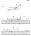
図8は、上記インダクタブリッジ102を用いてマザー基板201とアンテナ基板301とを接続した状態での断面図である。
FIG. 8 is a cross-sectional view of the
アンテナ基板301には上記アンテナ素子パターン91が形成されている。このアンテナ素子パターン91の端部、または端部から引き出した箇所にインダクタブリッジ102の第1コネクタ51が接続される。インダクタブリッジ102の第2コネクタ52はマザー基板201の上面に形成されている接続部に接続される。このマザー基板201上の接続部は面状に広がったグランド導体パターンGNDに導通している。
The
アンテナ基板301とマザー基板201との間にはマザー基板201に対する表面実装部品160がマザー基板201に実装されている。
A
インダクタブリッジ102のインダクタ部30は、グランドに接続される第2コネクタ52に近い位置に形成されている。すなわちアンテナ基板301から離れた位置に形成されている。このことにより、インダクタ部30における電磁波放射によるアンテナ特性の劣化を抑制できる。また、インダクタブリッジのアンテナ寄りの配線パターン21をアンテナの一部として作用させることができる。
The
また、図8に示すように、インダクタブリッジ102のうちインダクタ部30の形成位置がマザー基板201に対して垂直方向に延びるように設ければ、インダクタ部30のコイル軸Aはマザー基板201に対して平行となる。そのため、マザー基板201に形成されているグランド導体パターンGNDの影響を受けにくくできる。すなわち、インダクタ部30とグランド導体GNDとの不要結合が抑制され、グランド導体GNDに生じる渦電流が抑制される。インダクタ部30のコイル軸Aはマザー基板201に対して完全に平行で無くてもよく、少なくとも垂直にならないようにすれば、その角度に応じて上記効果は相当程度生じる。
Further, as shown in FIG. 8, if the forming position of the
なお、図7に示した構成のインダクタブリッジ102以外に、例えば図2に示したインダクタブリッジ101B等、他のインダクタブリッジも、逆F型アンテナのインダクタ部分を構成するために適用することができる。
In addition to the
図9は2つの基板をインダクタブリッジで接続した状態を示す図である。サブ基板302にはIC等の電子部品が実装されている。インダクタブリッジ101Dの第1接続部は基板302の上面に接続されていて、第2接続部はマザー基板202の上面に接続されている。なお、ここでは、サブ基板302が第1実装回路部材に相当し、マザー基板202が第2実装回路部材に相当する。
FIG. 9 is a diagram showing a state in which two boards are connected by an inductor bridge. Electronic components such as ICs are mounted on the sub-board 302. The first connection portion of the
インダクタブリッジ101Dのコネクタ以外の構成は、既に示したインダクタブリッジ101Aと同じである。
The configuration of the
以降に示す各実施形態での図を用いた説明は、第1の実施形態で示したインダクタブリッジとは構成の異なる部分についてのみ行う。したがって、以下に説明するインダクタブリッジ103~107,108A,108B,109の構成と、インダクタブリッジ101B~101D,102との構成を組み合わせたり、置換したりして実施することができる。 The description using the figures in each of the following embodiments will be given only for the portion having a configuration different from that of the inductor bridge shown in the first embodiment. Therefore, the configurations of the inductor bridges 103 to 107, 108A, 108B, 109 described below and the configurations of the inductor bridges 101B to 101D, 102 can be combined or replaced.
《第2の実施形態》
図10(A)は第2の実施形態に係るインダクタブリッジの外観斜視図、図10(B)はその分解斜視図である。このインダクタブリッジ103は、可撓性を有する平板状の素体10、第1コネクタ51および第2コネクタ52を備えている。図10(B)に表れているように、上記素体10は樹脂基材11,12,13,14が積層されることで構成される。樹脂基材12,13にはスパイラル状の導体パターン31,32によるインダクタ部が構成されている。スパイラル状の導体パターン31,32は、樹脂基材12,13の面に垂直方向(素体10の主面に垂直方向)にコイル軸が向くスパイラル状の導体パターンである。
<< Second Embodiment >>
10 (A) is an external perspective view of the inductor bridge according to the second embodiment, and FIG. 10 (B) is an exploded perspective view thereof. The
樹脂基材12には配線パターン21,22が形成されていて、樹脂基材14には配線パターン23が形成されている。配線パターン21の第1端はインダクタ部の導体パターン31の外周端につながり、導体パターン31の内周端はビア導体(層間接続導体)を介して導体パターン32の外周端につながり、導体パターン32の内周端は配線パターン23の第1端につながり、配線パターン23の第2端はビア導体を介して配線パターン22の第1端につながっている。導体パターン31,32は平面視で連続的には重ならないように配置されている。図10(C)はインダクタ部の導体パターンを示す部分平面図である。その他の構造は図1(B)に示したものと同じである。
このような構造により、層数の増加に伴うインダクタンスの増大の割には浮遊容量の増加が少なく、より高周波帯域までインダクタとして用いることができる。 With such a structure, the increase in stray capacitance is small for the increase in inductance due to the increase in the number of layers, and it can be used as an inductor up to a higher frequency band.
《第3の実施形態》
図11(A)は第3の実施形態に係るインダクタブリッジの外観斜視図、図11(B)はその分解斜視図である。このインダクタブリッジ104は、可撓性を有する平板状の素体10、第1コネクタ51および第2コネクタ52を備えている。図11(B)に表れているように、上記素体10は樹脂基材11,12,13,14が積層されることで構成される。樹脂基材12,13にはスパイラル状の導体パターン31,32によるインダクタ部が構成されている。スパイラル状の導体パターン31,32は、樹脂基材12,13の面に垂直方向(素体10の主面に垂直方向)にコイル軸が向くスパイラル状の導体パターンである。
<< Third Embodiment >>
11 (A) is an external perspective view of the inductor bridge according to the third embodiment, and FIG. 11 (B) is an exploded perspective view thereof. The
樹脂基材12には配線パターン21,22が形成されていて、樹脂基材14には配線パターン23が形成されている。配線パターン21の第1端はインダクタ部の導体パターン31の外周端につながり、導体パターン31の内周端はビア導体(層間接続導体)を介して導体パターン32の外周端につながり、導体パターン32の内周端は配線パターン23の第1端につながり、配線パターン23の第2端はビア導体を介して配線パターン22の第1端につながっている。導体パターン31,32は外周端同士および内周端同士が接続されている。すなわち導体パターン31,32は並列接続されている。その他の構造は図1(B)に示したものと同じである。
このような構造により、等価直列抵抗の低いインダクタを備えるインダクタブリッジが得られる。 Such a structure provides an inductor bridge with an inductor with low equivalent series resistance.
《第4の実施形態》
図12(A)は第4の実施形態に係るインダクタブリッジの外観斜視図、図12(B)はその分解斜視図である。このインダクタブリッジ105は、可撓性を有する平板状の素体10、第1コネクタ51および第2コネクタ52を備えている。図12(B)に表れているように、上記素体10は樹脂基材11,12が積層されることで構成される。樹脂基材12には素体の短手方向に延びるミアンダライン状の導体パターン31によるインダクタ部が構成されている。
<< Fourth Embodiment >>
12 (A) is an external perspective view of the inductor bridge according to the fourth embodiment, and FIG. 12 (B) is an exploded perspective view thereof. The
樹脂基材12には配線パターン21,22が形成されている。配線パターン21の第1端はインダクタ部の導体パターン31の第1端につながり、導体パターン31の第2端は配線パターン22の第1端につながり、配線パターン21,22の第2端はビア導体を介してコネクタ実装電極41,42につながっている。その他の構造は図1(B)に示したものと同じである。
図12(A)、図12(B)において、破線は屈曲位置(概略位置)を示している。インダクタ部の位置とそれ以外の位置との境界付近が屈曲部である。ミアンダライン状の導体パターン31によるインダクタ部は長手方向の剛性が高いので、インダクタ部の位置以外での屈曲が容易となる。また、このような構造により、素体10の屈曲によるインダクタンスの変化が抑制できる。
In FIGS. 12A and 12B, the broken line indicates the bending position (rough position). The bending portion is near the boundary between the position of the inductor portion and the position other than that. Since the inductor portion by the conductor line-shaped
なお、この第4の実施形態で示したインダクタ部の導体パターンとは異なり、互いに隣接する線路のそれぞれが素体の短手方向に延びるミアンダライン状の導体パターンでインダクタ部を構成すれば、素体の長手方向の柔軟性を高められる。また、素体の屈曲量に対するインダクタンスの変化量が抑制できる。 In addition, unlike the conductor pattern of the inductor portion shown in the fourth embodiment, if the inductor portion is configured with a meander line-shaped conductor pattern in which each of the adjacent lines extends in the lateral direction of the prime field, the inductor portion is formed. Increases the flexibility of the body in the longitudinal direction. In addition, the amount of change in inductance with respect to the amount of bending of the prime field can be suppressed.
《第5の実施形態》
図13(A)は第5の実施形態に係るインダクタブリッジの外観斜視図、図13(B)はその分解斜視図である。このインダクタブリッジ106は、可撓性を有する平板状の素体10、第1コネクタ51および第2コネクタ52を備えている。図13(B)に表れているように、上記素体10は樹脂基材11,12が積層されることで構成される。樹脂基材11,12には、主面に平行方向にコイル軸が向くヘリカル状の導体パターン31が形成されている。
<< Fifth Embodiment >>
13 (A) is an external perspective view of the inductor bridge according to the fifth embodiment, and FIG. 13 (B) is an exploded perspective view thereof. The
樹脂基材11には配線パターン21,22が形成されている。配線パターン21の第1端はインダクタ部の導体パターン31の第1端につながり、導体パターン31の第2端は配線パターン22の第1端につながり、配線パターン21,22の第2端はコネクタ実装電極41,42につながっている。その他の構造は図1(B)に示したものと同じである。
このように、素体10の主面に平行方向にコイル軸が向くヘリカル状の導体パターン31を形成することにより、このインダクタブリッジ106に導体が隣接しても、その導体に渦電流が生じ難く、周囲環境によるインダクタンスの変動が抑制される。
By forming the
《第6の実施形態》
図14(A)は第6の実施形態に係るインダクタブリッジの外観斜視図、図14(B)はその分解斜視図である。このインダクタブリッジ107は、可撓性を有する平板状の素体10、第1コネクタ51および第2コネクタ52を備えている。図14(B)に表れているように、上記素体10は樹脂基材11,12,13,14が積層されることで構成される。樹脂基材12,13には、主面に垂直方向にコイル軸が向くヘリカル状の導体パターン31,32が形成されている。樹脂基材12には開口APが形成されていて、この開口AP内にフェライト板による磁性体コア70が収納する。すなわち素体10内に磁性体コア70が埋設される。その他は図1(B)や図10(B)に示したものと同じである。
<< 6th Embodiment >>
14 (A) is an external perspective view of the inductor bridge according to the sixth embodiment, and FIG. 14 (B) is an exploded perspective view thereof. The
このように、磁性体コア70をインダクタ部の導体パターンの近傍に配置することにより、インダクタ部を小型化でき、小型のインダクタブリッジが構成できる。
By arranging the
《第7の実施形態》
図15(A)は第7の実施形態に係るインダクタブリッジの外観斜視図、図15(B)はその分解斜視図である。このインダクタブリッジ108Aは、可撓性を有する平板状の素体10、第1コネクタ51および第2コネクタ52を備えている。樹脂基材12にはスパイラル状の導体パターン31によるインダクタ部が構成されている。樹脂基材12には配線パターン21が形成されていて、樹脂基材13には配線パターン22が形成されている。配線パターン21の第1端はインダクタ部の導体パターン31の外周端につながり、導体パターン31の内周端はビア導体を介して配線パターン22の第1端につながっている。樹脂基材11にはコネクタ51,52を実装するためのコネクタ実装電極41,42が形成されている。これらコネクタ実装電極41,42はビア導体を介して配線パターン21,22の第2端にそれぞれ接続されている。
<< Seventh Embodiment >>
15 (A) is an external perspective view of the inductor bridge according to the seventh embodiment, and FIG. 15 (B) is an exploded perspective view thereof. The
樹脂基材11,14にはシールド導体パターン81,82が形成されている。このように、インダクタ部を層方向に挟む位置にシールド導体パターン81,82が形成されていることにより、インダクタ部が電磁シールドされて、安定した特性が得られる。
Shielded
なお、コネクタ51,52は同軸コネクタタイプのコネクタであり、中心導体はコネクタ実装電極41,42に接続され、外導体はシールド導体パターン81に接続される。
The
図16(A)は第7の実施形態に係るもう一つのインダクタブリッジ108Bの外観斜視図、図16(B)はその分解斜視図である。樹脂基材11,14に設けられているシールド導体パターン81,82には開口APが形成されている。その他は図15に示したインダクタブリッジ108Aと同じである。このようにシールド導体パターンは全体に連続して広がっていなくても、電磁シールド効果はある。開口APを複数形成して、メッシュ状のシールド導体パターンを設けてもよい。また、開口APをインダクタ部に対応する位置に配置することで、素体10の剛性を均一化することもできる。
16 (A) is an external perspective view of another
《第8の実施形態》
図17(A)は第8の実施形態に係るインダクタブリッジの外観斜視図、図17(B)はその分解斜視図である。また、図18はインダクタブリッジ109のインダクタ部の断面図である。このインダクタブリッジ109は、可撓性を有する平板状の素体10、第1コネクタ51および第2コネクタ52を備えている。樹脂基材13にはチップインダクタ39によるインダクタ部が構成されている。樹脂基材12にはチップインダクタ39が収納される開口APが形成されている。樹脂基材13の下面にはチップインダクタ39が接続される配線パターン21,22が形成されていて、樹脂基材11の上面にはコネクタ51,52を実装するためのコネクタ実装電極41,42が形成されている。これらコネクタ実装電極41,42はビア導体を介して配線パターン21,22にそれぞれ接続されている。
<< Eighth Embodiment >>
FIG. 17A is an external perspective view of the inductor bridge according to the eighth embodiment, and FIG. 17B is an exploded perspective view thereof. Further, FIG. 18 is a cross-sectional view of the inductor portion of the
このように、チップインダクタ39を素体10の面方向厚み方向のいずれについても中央に配置することにより、素体10の屈曲によるチップインダクタ39へ加わる応力が小さく、素体10の可撓性を維持したまま用いることができる。また、厚み一定のケーブルとして利用できる。
By arranging the
《第9の実施形態》
図19は第9の実施形態に係る電子機器401の筐体内部の構造を示す図であり、上部筐体191と下部筐体192とを分離して内部を露出させた状態での平面図である。この電子機器401は例えば携帯電話端末やタブレットPCであり、図1に示したインダクタブリッジ101Aを備えたものである。
<< Ninth Embodiment >>
FIG. 19 is a diagram showing the structure inside the housing of the
上部筐体191の内部にはプリント配線板171,181、バッテリーパック183等が収められている。プリント配線板171にはUHF帯アンテナ172、カメラモジュール176等も搭載されている。また、プリント配線板181にはUHF帯アンテナ182等が搭載されている。プリント配線板171とプリント配線板181とはケーブル184を介して接続されている。
A printed
プリント配線板181とUHF帯アンテナ182との間はインダクタブリッジ101Aで接続されている。インダクタブリッジ101Aの構成は図1に示したとおりである。なお、ここでは、UHF帯アンテナ182が第1実装回路部材に相当し、プリント配線板182が第2実装回路部材に相当する。
The printed
なお、プリント配線板171と181を接続するケーブル184にインダクタブリッジを適用してもよい。
An inductor bridge may be applied to the
《第10の実施形態》
図20は第10の実施形態に係るインダクタブリッジ110の分解斜視図である。このインダクタブリッジ110は、可撓性を有する平板状の素体、第1コネクタ51および第2コネクタ52を備えている。上記素体は樹脂基材11,12,13,14が積層されることで構成される。
<< 10th Embodiment >>
FIG. 20 is an exploded perspective view of the
図21は、上記インダクタブリッジ110の断面図であり、図20における一点鎖線部分での断面図である。
FIG. 21 is a cross-sectional view of the
樹脂基材11~14には導体パターン31~34によるインダクタ部が構成されている。導体パターン31~34は、樹脂基材11~14の面に垂直方向(素体の主面に垂直方向)にコイル軸が向く矩形ヘリカル状の導体パターンである。導体パターン31の一端には配線パターン21の第1端が接続されていて、導体パターン34の一端には配線パターン23の第1端が接続されている。
The
樹脂基材11にはコネクタ51,52を実装するためのコネクタ実装電極41,42が形成されている。コネクタ実装電極41は配線パターン21の第2端に接続されていて、コネクタ実装電極42はビア導体を介して配線パターン23の第2端に接続されている。
The
上記導体パターン31~34は、層間で対向する位置に形成されている。すなわち、積層方向に平面視したとき、複数の導体パターン31~34は重なる。これら複数の導体パターンのうち、第1コネクタ51(第1接続部)および第2コネクタ52(第2接続部)に経路上近い導体パターン31,34の線幅は他の層の導体パターン32,33の線幅より細い。
The
図21に表れているように、導体パターン31~34は、層間で対向する位置に形成されているので、層方向に隣接する導体パターン間に容量C1,C2,C3が生じる。導体パターン31,34の線幅は導体パターン32,33の線幅より細く、導体パターン31と導体パターン34との間に導体パターン32,33が挟まっているので、導体パターン31と導体パターン34との間に生じようとする容量C0は小さい。また、C1<C2、C3<C2の関係にある。
As shown in FIG. 21, since the
図22は上記インダクタブリッジ110の等価回路図である。図22においてインダクタL1,L2,L3,L4は上記導体パターン31,32,33,34のインダクタンス成分に相当し、キャパシタC1,C2,C3は図21に示したとおり、導体パターン31~34のうち、各層間に生じる容量成分、キャパシタC0は導体パターン31と導体パターン34との間に生じる容量成分にそれぞれ相当する。なお、ここでは導体パターンの抵抗成分については図示を省略している。
FIG. 22 is an equivalent circuit diagram of the
インダクタブリッジ110の自己共振周波数は、インダクタL1~L4等で示すインダクタンス成分、およびキャパシタC0~C3等で示す容量成分により定まるが、各部で生じる容量のうち、大きい電位差が掛かるキャパシタC0の容量が自己共振周波数の決定に対して支配的である。本実施形態によれば、上述のとおり、C0が効果的に抑制されるので、自己共振周波数は高くできる。
The self-resonant frequency of the
図23は自己共振周波数の変化について示す図である。図20、図21に示した導体パターン31~34の線幅が等しいとき、自己共振周波数はf0で示す周波数となる。本実施形態のように、導体パターン31,34の線幅を導体パターン32,33の線幅より細くすることで、自己共振周波数はf1で示すように高くなる。仮に、導体パターン31,34の線幅を導体パターン32,33の線幅より太くすると、自己共振周波数はf2で示すように低くなる。本実施形態のように、導体パターン31,34の線幅を導体パターン32,33の線幅より細くすることで、自己共振周波数が高くなって、通過帯域幅PBが広くなる。
FIG. 23 is a diagram showing changes in the self-resonant frequency. When the line widths of the
なお、導体パターン31,34の線幅を細くしても、その他の導体パターン32,33の線幅は太くできるので、インダクタ部におけるDCR(直流抵抗)の増大は抑えられる。
Even if the line widths of the
《第11の実施形態》
図24は第11の実施形態に係るインダクタブリッジ111の分解斜視図である。このインダクタブリッジ111は、可撓性を有する平板状の素体、第1コネクタ51および第2コネクタ52を備えている。上記素体は樹脂基材11,12,13,14が積層されることで構成される。
<< 11th Embodiment >>
FIG. 24 is an exploded perspective view of the
図25は、上記インダクタブリッジ111の断面図であり、図24における一点鎖線部分での断面図である。
FIG. 25 is a cross-sectional view of the
図20、図21に示したインダクタブリッジとは、導体パターン31,34の導体厚みが異なる。本実施形態では、導体パターン31,34の線路幅を細くした分、それらの導体厚みを厚くしてDCR(直流抵抗)が増大することを抑制している。この構造により、導体パターン31,34の線路幅を細くしてもDCRを低く抑えることができる。
The conductor thicknesses of the
《第12の実施形態》
図26は第12の実施形態に係るインダクタブリッジ112の分解斜視図である。このインダクタブリッジ112は、可撓性を有する平板状の素体、第1コネクタ51および第2コネクタ52を備えている。上記素体は樹脂基材11,12,13,14が積層されることで構成される。
<< Twelfth Embodiment >>
FIG. 26 is an exploded perspective view of the
図27は、上記インダクタブリッジ112の断面図であり、図26における一点鎖線部分での断面図である。
FIG. 27 is a cross-sectional view of the
本実施形態では、インダクタ部の導体パターン31~34の線幅は等しいが、層間距離が不均等である。すなわち、導体パターン31と導体パターン32との間の間隔は、導体パターン32と導体パターン33との間の間隔より広い。同様に、導体パターン33と導体パターン34との間の間隔は、導体パターン32と導体パターン33との間の間隔より広い。
In the present embodiment, the line widths of the
図28はインダクタブリッジ112の等価回路図である。図28において、インダクタLa、抵抗Raは、上記導体パターン31,32によるインダクタンス成分および抵抗成分に相当する。同様に、インダクタLb、抵抗Rbは、上記導体パターン32,33によるインダクタンス成分および抵抗成分に相当し、インダクタLc、抵抗Rc、は上記導体パターン33,34によるインダクタンス成分および抵抗成分に相当する。相互インダクタンスMは、インダクタLa-Lb間およびインダクタLb-Lc間にそれぞれ生じる。また、キャパシタCaは導体パターン31-32間に生じる容量成分に相当する。同様に、キャパシタCbは導体パターン32と導体パターン33との間に生じる容量成分、キャパシタCcは導体パターン33と導体パターン34間とのに生じる容量成分にそれぞれ相当する。
FIG. 28 is an equivalent circuit diagram of the
導体パターン31と導体パターン32との間隔および導体パターン33と導体パターン34との間隔は、導体パターン32と導体パターン33との間隔より広いので、上記容量Ca,Cb,Ccは、(Ca,Cc)<Cbの関係にある。
Since the distance between the
上記構造をシミュレーションしたところ、導体パターン31~34の層間距離を均等にした場合に比べて自己共振周波数が高まることがわかった。したがって、複数の導体パターンのうち、第1コネクタ51および第2コネクタ52に経路上近い導体パターン31,34と、この導体パターン31,34に対する隣接層の導体パターンとの間隔を、他の隣接層における導体パターン間の間隔より広くすることで、インダクタブリッジの通過帯域幅を広くすることができる。
When the above structure was simulated, it was found that the self-resonant frequency was higher than that in the case where the interlayer distances of the
なお、第10の実施形態、第11の実施形態および第12の実施形態では、インダクタ部を構成する導体パターンが4層であったが、3層であってもよいし、5層以上であってもよい。 In the tenth embodiment, the eleventh embodiment and the twelfth embodiment, the conductor pattern constituting the inductor portion has four layers, but it may be three layers or five or more layers. You may.
《第13の実施形態》
図29(A)、図29(B)は第13の実施形態に係るインダクタブリッジ113の斜視図である。図29(A)は上面を視た斜視図、図29(B)は下面を視た斜視図である。樹脂基材11の上面にスパイラル状の導体パターン31および配線パターン21,22が形成されていて、その下面に配線パターン23が形成されている。配線パターン23の第1端はスパイラル状の導体パターン31の内周端に、第2端は配線パターン22の端部にそれぞれビア導体を介して接続されている。
<< 13th Embodiment >>
29 (A) and 29 (B) are perspective views of the
図1に示した例では、2つの樹脂基材に導体パターン31および配線パターン21,22を形成したが、図29(A)(B)に示す例のように、1層の樹脂基材11に各種導体パターンを形成してもよい。必要に応じて最表面には導体パターンの保護のためのレジスト層が形成される。
In the example shown in FIG. 1, the
本実施形態によれば、両面に金属箔を張り付けた基板を用い、1層で作製することで、積層、圧着工程が不要で、工程を簡略化できる。 According to the present embodiment, by using a substrate with metal foils attached to both sides and manufacturing the substrate in one layer, the laminating and crimping steps are unnecessary, and the steps can be simplified.
《第14の実施形態》
図30は第14の実施形態に係る、インダクタブリッジおよびアンテナを備えた高周波回路の回路図である。この例ではアンテナANTの給電ラインに設けるインダクタL1としてインダクタブリッジ114を適用している。
<< 14th Embodiment >>
FIG. 30 is a circuit diagram of a high frequency circuit including an inductor bridge and an antenna according to a fourteenth embodiment. In this example, the
図31は、図30に示したアンテナANTおよびインダクタブリッジ114の実装(配置)構造を示す図である。
FIG. 31 is a diagram showing a mounting (arrangement) structure of the antenna ANT and the
アンテナ基板301にはアンテナ素子パターンが形成されている。このアンテナ素子パターンの所定箇所にインダクタブリッジ114の第1コネクタ51が接続される。インダクタブリッジ114の第2コネクタ52はマザー基板201の上面に形成されている接続部に接続される。
An antenna element pattern is formed on the
インダクタブリッジ114が近接するマザー基板201上には金属パターン(グランド導体パターンやRFICにつながる配線パターン等)83が形成されている。アンテナ基板301のアンテナ素子パターンの所定箇所は金属パターン83に接続されている。
A metal pattern (ground conductor pattern, wiring pattern connected to RFIC, etc.) 83 is formed on the
図31において、インダクタブリッジ114のインダクタ部30と第2コネクタ52との間の配線パターンと金属パターン83との間(図中Aで示す領域)は電位差が生じやすいので、この部分に生じる寄生容量が小さいことが好ましい。
In FIG. 31, a potential difference is likely to occur between the wiring pattern between the
図32(A)(B)は、図31に示したインダクタブリッジ114の実装構造および金属パターン83との位置関係を示す分解斜視図である。図32(A)(B)においては、インダクタブリッジの構造が異なるので、異なった符号を114A,114Bをそれぞれ付している。
32 (A) and 32 (B) are exploded perspective views showing the mounting structure of the
図32(A)(B)のいずれの構造においても、樹脂基材11,12,13にスパイラル状の導体パターン31、配線パターン21,22およびコネクタ実装電極41,42が形成されている。
In any of the structures of FIGS. 32 (A) and 32 (B),
図32(B)に示す例では、インダクタブリッジ114Bにおいて、RFICが接続される第2コネクタ52側の配線パターン22が第1コネクタ51側の配線パターン21に比べて金属パターン83(面状導体)に近い層に形成されている。コネクタ実装電極41と金属パターン83とは同電位であり、配線パターン22と金属パターン83との間に生じる寄生容量は大きい。そのため、アンテナ特性に与える影響が比較的大きい。
In the example shown in FIG. 32 (B), in the
これに対して、図32(A)に示す例では、インダクタブリッジ114Aにおいて、樹脂基材11にスパイラル状の導体パターン31、配線パターン22およびコネクタ実装電極41が形成されている。樹脂基材12には配線パターン21が形成されている。そして、樹脂基材13にコネクタ実装電極42が形成されている。
On the other hand, in the example shown in FIG. 32 (A), in the
図32(A)に示すインダクタブリッジの実装構造によれば、RFICが接続される第2コネクタ52側の配線パターン22およびインダクタ部30の導体パターン31が第1コネクタ51側の配線パターン21に比べて金属パターン83(面状導体)より離れた層に形成されている。そのため、配線パターン22および導体パターン31と金属パターン83との間に生じる寄生容量は小さく、アンテナ特性に与える影響が小さい。
According to the mounting structure of the inductor bridge shown in FIG. 32 (A), the
《第15の実施形態》
図33は第15の実施形態に係る、インダクタブリッジ115およびアンテナ基板301を備えた高周波回路の構造を示す図である。この例ではアンテナの給電ラインにインダクタブリッジ115を適用している。図33において、アンテナ基板301に接続される第1コネクタ51から遠い方の第2コネクタ52につながる導体パターンとアンテナ基板301との間(図中Aで示す領域)は電位差が大きいので、この部分に生じる寄生容量が小さいことが好ましい。
<< Fifteenth Embodiment >>
FIG. 33 is a diagram showing the structure of a high frequency circuit including the
図34(A)(B)は、図33に示したインダクタブリッジ115の実装構造およびアンテナ基板301との位置関係を示す分解斜視図である。図34(A)(B)においては、インダクタブリッジの構造が異なるので、異なった符号を115A,115Bをそれぞれ付している。
34 (A) and 34 (B) are exploded perspective views showing the mounting structure of the
図34(A)(B)のいずれの構造においても、樹脂基材11,12,13にスパイラル状の導体パターン31、配線パターン21,22およびコネクタ実装電極41,42が形成されている。第1コネクタ51はアンテナ基板のアンテナ素子パターン91の端部に接続される。
In any of the structures of FIGS. 34 (A) and 34 (B),
図34(B)に示す例では、インダクタブリッジ115Bにおいて、アンテナ素子パターン91の開放端付近が対向する第2コネクタ52側の配線パターン22が、第1コネクタ51側の配線パターン21に比べてアンテナ素子パターン91に近接する層に形成されている。そのため、配線パターン22とアンテナ素子パターン91との間に生じる寄生容量が大きく、アンテナ特性に与える影響が比較的大きい。
In the example shown in FIG. 34B, in the
これに対して、図34(A)に示す例では、インダクタブリッジ115Aにおいて、アンテナ素子パターン91の開放端付近が対向する第2コネクタ52側の配線パターン22が、第1コネクタ51側の配線パターン21に比べてアンテナ素子パターン91から離れた層に形成されている。そのため、配線パターン22とアンテナ素子パターン91との間に生じる寄生容量が小さく、アンテナ特性に与える影響が小さい。
On the other hand, in the example shown in FIG. 34 (A), in the
《第16の実施形態》
図35は第16の実施形態に係る、インダクタブリッジ116、アンテナ基板301およびマザー基板201を備えた高周波回路の構造を示す図である。この例ではアンテナの給電ラインにインダクタブリッジ116を適用している。図35において、第2コネクタ52は金属パターン83に接続されていて、アンテナ基板301に接続される第1コネクタ51につながる導体パターンとマザー基板201の金属パターン83との間(図中Aで示す領域)は電位差が大きいので、この部分に生じる寄生容量が小さいことが好ましい。
<< 16th Embodiment >>
FIG. 35 is a diagram showing a structure of a high frequency circuit including an
図36(A)(B)は、図35に示したインダクタブリッジ116の実装構造およびマザー基板201の金属パターン83との位置関係を示す分解斜視図である。図36(A)(B)においては、インダクタブリッジの構造が異なるので、異なった符号を116A,116Bをそれぞれ付している。
36 (A) and 36 (B) are exploded perspective views showing the mounting structure of the
図36(A)(B)のいずれの構造においても、樹脂基材11,12,13にスパイラル状の導体パターン31、配線パターン21,22およびコネクタ実装電極41,42が形成されている。第1コネクタ51はアンテナ基板301に接続される。
In any of the structures shown in FIGS. 36A and 36B,
図36(B)に示す例では、インダクタブリッジ116Bにおいて、アンテナ基板301に接続される第1コネクタ51につながる配線パターン21がマザー基板201の金属パターン83に近接する層に形成されている。そのため、配線パターン21と金属パターン83との間に生じる寄生容量が大きく、アンテナ特性に与える影響が比較的大きい。
In the example shown in FIG. 36B, in the
これに対して、図36(A)に示す例では、インダクタブリッジ116Aにおいて、アンテナ基板301に接続される第1コネクタ51につながる配線パターン21が、配線パターン22に比べて、マザー基板201の金属パターン83から遠い層に形成されている。そのため、配線パターン21と金属パターン83との間に生じる寄生容量が小さく、アンテナ特性に与える影響が小さい。
On the other hand, in the example shown in FIG. 36A, in the
《第17の実施形態》
図37は第17の実施形態に係る、インダクタブリッジ117、アンテナ基板301および金属部材84を備えた高周波回路の構造を示す図である。この例ではアンテナの給電ラインにインダクタブリッジ117を適用している。図37において、アンテナ基板301に接続される第1コネクタ51につながる導体パターンと金属部材(例えばバッテリーパックや液晶表示パネルのシールド板等)84との間(図中Aで示す領域)はアンテナ特性に与える影響が大きいので、この部分に生じる寄生容量が小さいことが好ましい。
<< 17th Embodiment >>
FIG. 37 is a diagram showing a structure of a high frequency circuit including an
図38(A)(B)は、図37に示したインダクタブリッジ117の実装構造および金属部材84との位置関係を示す分解斜視図である。図38(A)(B)においては、インダクタブリッジの構造が異なるので、異なった符号を117A,117Bをそれぞれ付している。
38 (A) and 38 (B) are exploded perspective views showing the mounting structure of the
図38(A)(B)のいずれの構造においても、樹脂基材11,12,13にスパイラル状の導体パターン31、配線パターン21,22およびコネクタ実装電極41,42が形成されている。第1コネクタ51はアンテナ基板301に接続される。
In any of the structures of FIGS. 38A and 38B,
図38(B)に示す例では、インダクタブリッジ117Bにおいて、アンテナ基板301に接続される第1コネクタ51につながる配線パターン21が金属部材84に近接する層に形成されている。そのため、配線パターン21と金属部材84との間に生じる寄生容量が大きく、アンテナ特性に与える影響が比較的大きい。
In the example shown in FIG. 38B, in the
これに対して、図38(A)に示す例では、インダクタブリッジ117Aにおいて、アンテナ基板301に接続される第1コネクタ51につながる配線パターン21が、配線パターン22に比べて、金属部材84から遠い層に形成されている。そのため、配線パターン21と金属部材84との間に生じる寄生容量が小さく、アンテナ特性に与える影響が小さい。
On the other hand, in the example shown in FIG. 38 (A), in the
《第18の実施形態》
図39(A)(B)は第18の実施形態に係るインダクタブリッジ118A,118Bの分解斜視図である。樹脂基材11,12にスパイラル状の導体パターン31,32、配線パターン21,22,23が形成されている。
<< 18th Embodiment >>
39 (A) and 39 (B) are exploded perspective views of the inductor bridges 118A and 118B according to the eighteenth embodiment.
このように、スパイラル状の導体パターン31,32を2層の樹脂基材11,12に形成するとともに、配線パターンもこの2層の樹脂基材11,12に形成することによって、2層の樹脂基材を積層するだけでインダクタブリッジを構成できる。なお、最表面には導体パターンの保護のためのレジスト層を形成することが好ましい。
In this way, the
《第19の実施形態》
図40は第19の実施形態に係る、インダクタブリッジ119、アンテナ基板301および金属部材84を備えた高周波回路の構造を示す図である。この例ではアンテナの給電ラインにインダクタブリッジ119を適用している。 図41(A)は、図40に示したインダクタブリッジ119の斜視図、図41(B)はインダクタブリッジ119Aの構造および金属部材84との位置関係を示す分解斜視図である。図41(C)はインダクタブリッジ119Bの構造および金属部材84との位置関係を示す分解斜視図である。図41(B)(C)においては、インダクタブリッジの構造が異なるので、異なった符号を119A,119Bをそれぞれ付している。
<< 19th Embodiment >>
FIG. 40 is a diagram showing a structure of a high frequency circuit including an
図41(A)(B)のいずれの構造においても、樹脂基材11,12,13にスパイラル状の導体パターン31,32、配線パターン21,22およびコネクタ実装電極41,42が形成されている。第1コネクタ51はアンテナ基板301に接続される。
In any of the structures of FIGS. 41 (A) and 41 (B),
図41(C)に示す例では、インダクタブリッジ119Bにおいて、金属部材84に近い側の樹脂基材12に形成されている導体パターン32のターン数が、遠い側の樹脂基材11に形成されている導体パターン31のターン数より多いので、インダクタ部に生じる磁界が金属部材84によって妨げられやすい。そのため所定のインダクタンスを得にくい。また、導体パターン32と金属部材84との間に生じる寄生容量が大きい。
In the example shown in FIG. 41 (C), in the
これに対して、図41(B)に示す例では、インダクタブリッジ119Aにおいて、金属部材84に近い側の樹脂基材12に形成されている導体パターン32のターン数が、遠い側の樹脂基材11に形成されている導体パターン31のターン数より少ないので、インダクタ部に生じる磁界が金属部材84によって妨げられにくい。そのためインダクタンスの低下が少ない。また、導体パターン32と金属部材84との間に生じる寄生容量も小さい。
On the other hand, in the example shown in FIG. 41 (B), in the
《第20の実施形態》
図42は、第20の実施形態に係るインダクタブリッジ120、アンテナ基板301および金属部材84を備えた高周波回路の構造を示す図である。この例ではアンテナの給電ラインにインダクタブリッジ120を適用している。 図43(A)はインダクタブリッジ120の斜視図、図43(B)はインダクタブリッジ120の構造および金属部材84との位置関係を示す分解斜視図である。樹脂基材11,12,13にスパイラル状の導体パターン31,32、配線パターン21,22およびコネクタ実装電極41,42が形成されている。樹脂基材11,12,13が積層されて素体10が構成される。第1コネクタ51はアンテナ基板301に接続される。
<< 20th Embodiment >>
FIG. 42 is a diagram showing the structure of a high frequency circuit including the
図44(A)は、インダクタブリッジ120の素体10の断面図である。この例では導体パターン31と導体パターン32とが層方向に対向している。図44(B)はインダクタブリッジ120の等価回路図である。ここでインダクタLは主に導体パターン31,32によるインダクタンスに相当し、キャパシタCは導体パターン31と導体パターン32との間に生じる容量に相当する。この回路構成により、帯域除去フィルタ(BEF)として作用し、所定の周波数帯域を減衰させる機能をもたせることができる。
FIG. 44A is a cross-sectional view of the
図45(A)は、上記インダクタブリッジ120とは内部の構造が少し異なるインダクタブリッジの断面図、図45(B)は、その場合のインダクタブリッジの等価回路図である。この例では、図44(A)に示した例に比べ、導体パターン31と導体パターン32との層方向の対向面積が少ない。図45(B)に示すインダクタLは主に導体パターン31,32によるインダクタンスに相当し、キャパシタCは導体パターン31,32と金属部材84との間に生じる容量に相当する。この回路構成により、低域通過フィルタ(LPF)として作用し、不要な高周波(高調波)成分を減衰させる機能をもたせることができる。
45 (A) is a cross-sectional view of an inductor bridge whose internal structure is slightly different from that of the
《第21の実施形態》
図46は、第21の実施形態に係るインダクタブリッジ121、アンテナ基板301、金属部材84およびマザー基板201を備えた高周波回路の構造を示す図である。図47はインダクタブリッジ121の斜視図である。この例ではアンテナの給電ラインにインダクタブリッジ121を適用している。
<< 21st Embodiment >>
FIG. 46 is a diagram showing a structure of a high frequency circuit including an
図48(A)(B)はインダクタブリッジ121の部分分解斜視図および屈曲位置を示す図である。いずれも、樹脂基材11,12,13にスパイラル状の導体パターン31、配線パターン21,22およびコネクタ実装電極42が形成されている。
48 (A) and 48 (B) are a partially disassembled perspective view of the
図48(B)に示すように配線パターン21の途中位置で屈曲しようとすると、想定外の位置に応力を受けることにより、スパイラル状の導体パターン形成範囲にまで屈曲位置がずれてしまうことがある。その場合には、スパイラル状導体パターン31の変形によってインダクタンスが変動してしまう。
As shown in FIG. 48 (B), if an attempt is made to bend at an intermediate position of the
一方、図48(A)に示すように、スパイラル状の導体パターン31と配線パターン22との層間接続導体(ビア)の位置でインダクタブリッジを屈曲すれば、屈曲位置が変動することなく、屈曲位置がばらつかないため、インダクタンスの想定外の変動が抑えられる。
On the other hand, as shown in FIG. 48 (A), if the inductor bridge is bent at the position of the interlayer connecting conductor (via) between the
図49(A)(B)はインダクタブリッジ121の別の部分分解斜視図および屈曲位置を示す図である。
49 (A) and 49 (B) are another partially exploded perspective view of the
図49(B)に示すように、想定外の位置に応力を受けて、スパイラル状の導体パターン形成範囲にまで屈曲位置がずれてしまうと、スパイラル状導体パターン31の変形によってインダクタンスが変動してしまう。
As shown in FIG. 49B, when stress is applied to an unexpected position and the bending position shifts to the spiral conductor pattern forming range, the inductance fluctuates due to the deformation of the
一方、図49(A)に示すように、配線パターン21の途中位置で屈曲されるように、ダミーの層間接続導体(ビア)VIAを形成しておけば、この位置でインダクタブリッジが屈曲される。このことにより、屈曲位置が変動することなく、屈曲位置がばらつかないため、インダクタンスの想定外の変動が抑えられる。
On the other hand, as shown in FIG. 49 (A), if a dummy interlayer connection conductor (via) VIA is formed so as to be bent at an intermediate position of the
《第22の実施形態》
図50(A)は第22の実施形態に係るインダクタブリッジ123の斜視図、図50(B)はその分解斜視図である。このインダクタブリッジ123は第1回路と第2回路との間を2端子コネクタでブリッジ接続するための素子である。図50(A)に表れているように、このインダクタブリッジ123は、可撓性を有する平板状の素体10、第1の2端子コネクタ53および第2の2端子コネクタ54を備えている。
<< 22nd Embodiment >>
50 (A) is a perspective view of the
図50(B)に表れているように、素体10は液晶ポリマー(LCP)の樹脂基材11,12,13,14が積層されることで構成される。樹脂基材12,13には導体パターン31,32によるインダクタ部が構成されている。導体パターン31,32は、樹脂基材12の面に垂直方向(素体10の主面に垂直方向)にコイル軸が向くスパイラル状の導体パターンである。
As shown in FIG. 50 (B), the
樹脂基材12には配線パターン21,22が形成されていて、樹脂基材14には配線パターン23が形成されている。樹脂基材11にはコネクタ実装電極41S,42Sおよびグランド電極40が形成されている。2端子コネクタ53,54の中心導体はコネクタ実装電極41S,42Sにそれぞれ接続され、コネクタ実装電極41S,42Sの外導体はグランド電極40に接続される。
グランド電極40は、インダクタ部をシールドする機能があり、外部の回路との不要結合を抑制する。また、このインダクタブリッジを接続する基板等に形成されている導体や金属部材との不要結合を抑制する。
The
導体パターン31のインダクタンスは導体パターン32のインダクタンスより小さい、インダクタンスの小さい方の導体パターンがグランド電極40に近接することで、グランド電極40に生じる渦電流が少なくてすむ。
The inductance of the
《第23の実施形態》
図51(A)は第23の実施形態に係るインダクタブリッジ124の斜視図、図51(B)はその分解斜視図である。図51(B)に表れているように、素体10は樹脂基材11,12,13,14が積層されることで構成される。樹脂基材12,13には導体パターン31,32によるインダクタ部が構成されている。樹脂基材12には配線パターン21,22が形成されていて、樹脂基材14には配線パターン23が形成されている。樹脂基材11にはコネクタ実装電極41,42およびグランド電極40が形成されている。グランド電極40には導電性両面テープ43が貼付されている。
<< 23rd Embodiment >>
51 (A) is a perspective view of the
このインダクタブリッジ124を電子機器に組み込んだ状態で、導電性両面テープ43が組み込み先電子機器筐体内のグランド電極や金属部材に貼付される。これにより、2端子コネクタを用いることなく、グランド接続が行われる。なお、導電性両面テープ以外に導電性接着剤を用いて、グランド接続を行ってもよい。
With the
《第24の実施形態》
図52(A)は第24の実施形態に係るインダクタブリッジ125の外観斜視図である。図52(B)は第24の実施形態に係るインダクタブリッジ125の分解平面図である。インダクタブリッジ125は屈曲線LOF1で山折り、屈曲線LOF2で谷折りされ、例えば図8に示したような形態で使用される。
<< 24th Embodiment >>
FIG. 52 (A) is an external perspective view of the
素体10は樹脂基材11,12,13,14,15が積層されることで形成される。樹脂基材11の上面にはレジスト層61が形成され、樹脂基材15の下面にはレジスト層62が形成される。レジスト層61、62にはそれぞれ開口部が形成されている。樹脂基材11の上面には導体パターン31が形成されている。樹脂基材12~15の下面にはループ状の導体パターン32~35が形成されている。樹脂基材11~15には層間接続導体V1~V5が形成されている。樹脂基材11の上面にはコネクタ実装電極41、樹脂基材15の下面にはコネクタ実装電極42がそれぞれ形成されている。
The
樹脂基材11において導体パターン31は第1端がコネクタ実装電極41に接続され、第2端が層間接続導体V1に接続される。層間接続導体V1は樹脂基材12に形成された導体パターン32の第1端に接続される。樹脂基材12において層間接続導体V2は導体パターン32の第1端に接続される。導体パターン32の第2端は樹脂基材13に形成された層間接続導体V3に接続される。樹脂基材13において層間接続導体V3は導体パターン33の第1端に接続される。導体パターン33の第2端は樹脂基材14に形成された層間接続導体V4に接続される。樹脂基材14において層間接続導体V4は導体パターン34の第1端に接続される。導体パターン34の第2端は樹脂基材15に形成された層間接続導体V5に接続される。樹脂基材15において層間接続導体V5は導体パターン35の第1端に接続される。導体パターン35の第2端はコネクタ実装電極42に接続される。
In the
コネクタ実装電極41,42は、レジスト層61,62の開口部を経由してコネクタ51,52に接続される。これらの導体パターンおよび層間接続導体にて積層型コイルパターンによるインダクタ部が構成されている。
The
本実施形態によれば、以下に述べるような多くの作用効果を奏する。 According to this embodiment, many functions and effects as described below are exhibited.
図53(A)(B)は上記屈曲部付近における導体パターンに掛かる応力について示す図である。図53(C)はインダクタブリッジ125の屈曲状態での斜視図である。図53(A)(B)においては導体パターン32,34の一部を代表的に表している。図53(A)に示すように、インダクタブリッジ125の導体パターンのうち、屈曲線LOF1,LOF2と交差する部分は、屈曲線LOF1,LOF2に対して直交しないで所定角度で交差するように、導体パターンが形成されている。つまり、平面視でインダクタパターンは楕円形(リーフ形状)の概形を有しており、その長軸は各屈曲線LOF1,LOF2に対して非垂直である(楕円形状の長軸および短軸が各屈曲線LOF1,LOF2に対して斜めになる)ようにパターニングされている。
FIGS. 53 (A) and 53 (B) are views showing the stress applied to the conductor pattern in the vicinity of the bent portion. FIG. 53C is a perspective view of the
屈曲線LOF1,LOF2と交差する導体パターンの部分を上記形状にすることにより、素体10の屈曲時に発生する応力を分散させることができる。具体的には、図53(A)に示すように、樹脂基材12の長手方向に掛かる応力をFで表すとき、導体パターン32の屈曲線LOF1と交差する位置での導体パターン32に掛かる応力はFcosθになる。すなわちFより低減される。
By forming the portion of the conductor pattern that intersects the bending lines LOF1 and LOF2 into the above shape, the stress generated when the
また、図53(B)に示すように、導体パターン34は、屈曲線LOF2の近傍において導体パターンが湾曲している。このような部分を設けることにより、屈曲部における樹脂基材14の変形に対し、導体パターン34が追随変形するので断線しにくい。例えば導体パターン34は素体10の厚み中央より下層に存在するため、屈曲線LOF2での屈曲により、導体パターン34には引っ張り応力が掛かる。そのため、図53(B)において破線で示すように、導体パターン34は屈曲線LOF2との交差位置付近が真っ直ぐに伸びようとする。このように、導体パターンの屈曲部が予め湾曲しているので、言わば「伸びしろ」があり、導体パターンが変形し易い。この作用によって導体パターンに掛かる応力はさらに緩和される。
Further, as shown in FIG. 53 (B), in the
また、図52(B)に示したとおり、層間接続導体V1~V5は、いずれも屈曲線LOF2よりもコネクタ実装電極42側に設けられている。屈曲線LOF2に近い位置に配置される層間接続導体V3,V5に接続される導体パターン33,35は、導体パターン33,35が屈曲線LOF2と重なる部分と層間接続導体V3,V5部との間において、図中破線で囲んで示すように、湾曲形状(迂回形状)になっている。導体パターンをこのような形状にすることにより、屈曲線LOF2で素体10が屈曲されたときに、屈曲による応力は層間接続導体V3,V5に直接的に伝わらないので、層間接続導体V3,V5と導体パターン33,35との間の破断が起こりにくい。なお、導体パターン32,34については、屈曲線LOF2から層間接続導体V2,V4までの距離が大きいので、上記湾曲形状(迂回形状)が無くても断線し難い。
Further, as shown in FIG. 52B, the interlayer connection conductors V1 to V5 are all provided on the
図54(A)はインダクタブリッジ125の平面図である。図54(A)においては、インダクタ部の導体パターンと屈曲位置との関係を示すために、導体パターンの楕円形状を表している。図54(B)はインダクタブリッジ125の屈曲状態での斜視図である。
FIG. 54 (A) is a plan view of the
図54(A)に示すように、インダクタブリッジ125において、インダクタ部の楕円形状の導体パターンは、その長軸がX軸に対して傾斜している。そのため、インダクタ部の導体パターンは、領域Aから領域Bにかけて、さらに領域Bから領域Cにかけて、Y軸の正方向にシフトしている。このような構造にすることにより、楕円形状の長軸がX軸方向を向いている場合に比べて、隣接領域を亘る導体パターンの線間距離が大きくなる。例えば、楕円形状の長軸がX軸方向を向いていると、領域Aにある導体パターンと領域Cにある導体パターンとは、屈曲線LOF1で山折り、屈曲線LOF2で谷折りされることで、領域Aの導体パターン部分と領域Cの導体パターン部分とが接近する。これに対し、本実施形態によれば、図54(A)において破線で示す部分の導体パターン間の間隔は上記屈曲によってもあまり接近しない。そのため、インダクタ部の導体パターンの線間容量が大きくならず、自己共振周波数を高く保つことができる。
As shown in FIG. 54 (A), in the
また、素体10がフレキシブル性を有すると、素体10の領域Aと領域Bとの成す角度(屈曲角度)、領域Bと領域Cとの成す角度(屈曲角度)は、一定に保ちにくい。上述のとおり、本実施形態によれば、屈曲による線間容量の増大が少ないので、屈曲形状のばらつきによるインダクタ素子として電気的特性の変化も少ない。
Further, when the
また、図52(B)と図54(A)(B)とを参照すれば明らかなように、領域Bには層間接続導体が形成されていない。層間接続導体は硬い材料で構成されていることから、層間接続導体が形成されている付近は、層間接続導体が形成されていない部分に比べて変形しにくい。そのため、領域Bに層間接続導体が形成されている構造と比べて、屈曲線LOF1,LOF2での屈曲が容易となる。 Further, as is clear from FIGS. 52 (B) and 54 (A) (B), the interlayer connecting conductor is not formed in the region B. Since the interlayer connecting conductor is made of a hard material, the vicinity where the interlayer connecting conductor is formed is less likely to be deformed than the portion where the interlayer connecting conductor is not formed. Therefore, as compared with the structure in which the interlayer connecting conductor is formed in the region B, the bending at the bending lines LOF1 and LOF2 becomes easier.
また、領域Bに層間接続導体が存在すると、インダクタ部の導体パターンの途中に、断面視における層間接続導体による角部(段差形状部)が形成されることになる。このような導体パターンの角部は高周波でのロスの原因となる。本実施形態においては、インダクタ部の導体パターンの途中に層間接続導体が存在しないので、上記ロスの発生を抑制できる。 Further, when the interlayer connecting conductor is present in the region B, a corner portion (step-shaped portion) due to the interlayer connecting conductor in the cross-sectional view is formed in the middle of the conductor pattern of the inductor portion. The corners of such a conductor pattern cause loss at high frequencies. In the present embodiment, since the interlayer connecting conductor does not exist in the middle of the conductor pattern of the inductor portion, the occurrence of the above loss can be suppressed.
なお、図52~図54に示した例では、平行な2本の屈曲線LOF1,LOF2に沿ってインダクタブリッジを屈曲させる例を示したが、屈曲線が1本である場合にも同様に適用され、同様の効果を奏する。 In the examples shown in FIGS. 52 to 54, an example in which the inductor bridge is bent along two parallel bending lines LOF1 and LOF2 is shown, but the same applies to the case where there is only one bending line. And has the same effect.
《第25の実施形態》
図55(A)は第25の実施形態に係るインダクタブリッジ126の斜視図、図55(B)はその分解斜視図である。インダクタブリッジ126は素体10内にインダクタが構成されている。素体10の外面にはコネクタ51,52が設けられている。図55(B)に表れているように、上記素体10は樹脂基材11,12,13,14が積層されることで構成される。樹脂基材12,13の下面には導体パターン31,32によるインダクタ部が構成されている。また、樹脂基材12,13には配線パターン21,22が形成されている。樹脂基材11にはコネクタ実装電極42が形成されていて、樹脂基材14にはコネクタ実装電極41が形成されている。
<< 25th Embodiment >>
FIG. 55 (A) is a perspective view of the
これまでに示した各実施形態では、素体10の両端部にそれぞれ接続部が設けられた例を示したが、本実施形態では、2つの接続部のうち少なくとも一方は素体10の端部とは異なる位置に設けられている。
In each of the embodiments shown so far, an example in which connecting portions are provided at both ends of the
本実施形態のインダクタブリッジ126の特徴は、電気的には、2つのコネクタ51,52の間にインダクタが接続されているが、機械的構造においては、2つのコネクタ51,52の間でない個所にインダクタ部が配置されていること、および2つのコネクタ51,52の間でない個所を屈曲できるようにしたこと等である。
The feature of the
図56(A)は、上記インダクタブリッジ126のインダクタ部(2つのコネクタ51,52の間でない部分)をインダクタ部以外の部分から屈曲させた状態の斜視図である。図56(B)(C)は、インダクタブリッジ126が他の部品と共にマザー基板201に実装された状態を示す図である。マザー基板201については断面を表している。
FIG. 56A is a perspective view showing a state in which the inductor portion (a portion not between the two
図56(B)に示す例では、マザー基板201上の接続部にインダクタブリッジ126のコネクタ51が接続された状態で、マザー基板201にインダクタブリッジ126が取り付けられている。このインダクタブリッジ126のコネクタ52にはサブ基板302が接続されている。マザー基板201には表面実装部品160が実装されていて、この表面実装部品160とサブ基板302との間隙にインダクタブリッジ126のインダクタ部が配置されている。
In the example shown in FIG. 56B, the
インダクタ部は導体パターンが多いので曲げにくいのに対し、インダクタ部でない部分は曲げやすい。そのため、図56(A)(B)に示すようにインダクタ部とインダクタ部でない部分との境界で屈曲させやすい。このインダクタ部はマザー基板201に対して垂直に立っているので、部品間の狭い空間に配置しやすい。また、平面占有面積を縮小化できる。さらに、マザー基板201に形成されている金属パターン(グランド導体パターン等)83が形成されている場合に、インダクタブリッジ126のインダクタ部のコイル軸は金属パターン83と直交するので、金属パターン83に渦電流が生じ難く、損失およびインダクタンスの変動が抑制される。
Since the inductor part has many conductor patterns, it is difficult to bend, whereas the part that is not the inductor part is easy to bend. Therefore, as shown in FIGS. 56A and 56B, it is easy to bend at the boundary between the inductor portion and the portion other than the inductor portion. Since this inductor portion stands perpendicular to the
図56(C)に示す例では、インダクタブリッジ126を平板状態でマザー基板201に取り付けている。このように、インダクタブリッジ126は必要に応じて屈曲させないで配置してもよい。
In the example shown in FIG. 56C, the
《第26の実施形態》
図57(A)は第26の実施形態に係るインダクタブリッジ127の斜視図、図57(B)はその分解斜視図である。インダクタブリッジ127は素体10内にインダクタが構成されている。素体10の外面にはコネクタ51,52が設けられている。図57(B)に表れているように、上記素体10は樹脂基材11,12,13,14が積層されることで構成される。樹脂基材12,13の下面には導体パターン31,32によるインダクタ部が構成されている。また、樹脂基材12,13には配線パターン21,22が形成されている。樹脂基材11にはコネクタ実装電極42が形成されていて、樹脂基材14にはコネクタ実装電極41が形成されている。
<< 26th Embodiment >>
57 (A) is a perspective view of the
本実施形態のインダクタブリッジ127の特徴は、電気的には、2つのコネクタ51,52の間にインダクタが接続されているが、機械的構造においては、2つのコネクタ51,52を結ぶ線上とは異なる個所にインダクタ部が配置されていること、2つのコネクタ51,52を結ぶ線上でない個所を屈曲できるようにしたこと、および、2つのコネクタ51,52を結ぶ線に平行な線に沿って屈曲できるようにしたこと等である。
The feature of the
図58(A)(B)は、上記インダクタブリッジ127が他の部品と共にマザー基板201に実装された状態を示す図である。インダクタブリッジ127の第1コネクタ51はマザー基板201上の接続部に接続されている。インダクタブリッジ127の第2コネクタ52にはサブ基板302が接続されている。マザー基板201には実装部品161が実装されている。
58 (A) and 58 (B) are views showing a state in which the
特に、図58(A)に示す例では、実装部品161と干渉しないように、インダクタブリッジ127のインダクタ部が起立している。このインダクタ部はマザー基板201に対して垂直に立っているので、部品間の狭い空間に配置しやすい。
In particular, in the example shown in FIG. 58 (A), the inductor portion of the
また、図58(B)に示す例では、インダクタブリッジ127のインダクタ部が起立することなく、インダクタ部が実装部品161と干渉しないように、インダクタブリッジ127がマザー基板201上に配置されている。
Further, in the example shown in FIG. 58B, the
このように、インダクタ部を2つのコネクタ間を結ぶ線上とは異なる個所に形成してもよい。この構造により、2つのコネクタ間の距離が確保できない場合でも、所定の大きなインダクタンスを生じさせることができる。 In this way, the inductor portion may be formed at a position different from the line connecting the two connectors. With this structure, even if the distance between the two connectors cannot be secured, a predetermined large inductance can be generated.
ANT…アンテナ
AP…開口
H1,H3…孔
L1…インダクタ
V1~V5…層間接続導体
10…素体
11,12,13,14…樹脂基材
21,22,23…配線パターン
30…インダクタ部
31,32,33,34,35…導体パターン
39…チップインダクタ
40…グランド電極
41,42…コネクタ実装電極
43…導電性両面テープ
51…第1コネクタ
52…第2コネクタ
53,54…2端子コネクタ
61,62…レジスト層
70…磁性体コア
81,82…シールド導体パターン
83…金属パターン
84…金属部材
91…アンテナ素子パターン
101A~101D…インダクタブリッジ
102~107…インダクタブリッジ
108A,108B…インダクタブリッジ
109~127…インダクタブリッジ
160,161…実装部品
171,181…プリント配線板
172…UHF帯アンテナ
176…カメラモジュール
182…UHF帯アンテナ
183…バッテリーパック
184…ケーブル
191…上部筐体
192…下部筐体
201…マザー基板
202…マザー基板
301…アンテナ基板
302…基板
401…電子機器
ANT ... Antenna AP ... Opening H1, H3 ... Hole L1 ... inductor V1 to V5 ...
Claims (8)
複数の樹脂基材の積層体からなり、可撓性を有する平板状の素体と、
前記第1実装回路部材に接続される第1接続部と、
前記第2実装回路部材に接続される第2接続部と、
前記素体の前記第1接続部と前記第2接続部との間に接続され、前記複数の樹脂基材の積層方向に巻回軸を有する導体パターンからなるインダクタ部と、
前記第1接続部と前記第2接続部との間に設けられ、前記インダクタ部を前記第1接続部および前記第2接続部に接続する配線パターンと、
を備え、
前記インダクタ部は4層以上の層に亘ってスパイラル状に形成された導体パターンを備え、
前記第1接続部および前記第2接続部の少なくとも一方に経路上最も近い容量であって、層方向に隣接する2つの前記導体パターンにより形成される容量が前記第1接続部および前記第2接続部から経路上離れた容量であって、層方向に隣接する2つの前記導体パターンにより形成される容量と比較して小さく、
前記第1接続部および前記第2接続部の少なくとも一方に経路上最も近い前記容量を形成する前記2つの導体パターンの前記層方向の間隔は、前記第1接続部および前記第2接続部から経路上離れた前記容量を形成する前記2つの導体パターンの前記層方向の間隔より大きい、
インダクタブリッジ。 An inductor bridge that is an element for bridging the first mounting circuit member and the second mounting circuit member.
A flat plate-like prime field consisting of a laminate of multiple resin substrates and having flexibility,
The first connection portion connected to the first mounting circuit member and
The second connection portion connected to the second mounting circuit member and
An inductor portion formed of a conductor pattern connected between the first connection portion and the second connection portion of the prime field and having a winding axis in the stacking direction of the plurality of resin substrates.
A wiring pattern provided between the first connection portion and the second connection portion and connecting the inductor portion to the first connection portion and the second connection portion.
Equipped with
The inductor portion has a conductor pattern formed in a spiral shape over four or more layers.
The capacitance closest to at least one of the first connecting portion and the second connecting portion on the path and formed by the two conductor patterns adjacent in the layer direction is the first connecting portion and the second connecting portion. The capacitance away from the section on the path is smaller than the capacitance formed by the two conductor patterns adjacent in the layer direction .
The distance between the two conductor patterns forming the capacitance closest to at least one of the first connection portion and the second connection portion in the layer direction is the path from the first connection portion and the second connection portion. Greater than the distance in the layer direction of the two conductor patterns forming the capacitance apart from each other.
Inductor bridge.
請求項1に記載のインダクタブリッジ。 The line width of the conductor pattern closest to at least one of the first connection portion and the second connection portion on the path is larger than the line width of the conductor pattern separated from the first connection portion and the second connection portion on the path. thin,
The inductor bridge according to claim 1.
複数の樹脂基材の積層体からなり、可撓性を有する平板状の素体と、
前記第1実装回路部材に接続される第1接続部と、
前記第2実装回路部材に接続される第2接続部と、
前記素体の前記第1接続部と前記第2接続部との間に接続され、前記複数の樹脂基材の積層方向に巻回軸を有する導体パターンからなるインダクタ部と、
前記第1接続部と前記第2接続部との間に設けられ、前記インダクタ部を前記第1接続部および前記第2接続部に接続する配線パターンと、
を備え、
前記インダクタ部は4層以上の層に亘ってスパイラル状に形成された導体パターンを備え、
最も表層に近い前記導体パターンが層方向に近接する前記導体パターンと形成する容量が、内層に位置する導体パターンが前記層方向において内層側に近接する導体パターンと形成する容量と比較して小さく、
最も表層に近い前記導体パターンとこの導体パターンに前記層方向に近接する前記導体パターンとの間隔は、内層に位置する導体パターンとこの導体パターンに前記層方向において内層側に近接する導体パターンとの間隔より大きい、
インダクタブリッジ。 An inductor bridge that is an element for bridging the first mounting circuit member and the second mounting circuit member.
A flat plate-like prime field consisting of a laminate of multiple resin substrates and having flexibility,
The first connection portion connected to the first mounting circuit member and
The second connection portion connected to the second mounting circuit member and
An inductor portion formed of a conductor pattern connected between the first connection portion and the second connection portion of the prime field and having a winding axis in the stacking direction of the plurality of resin substrates.
A wiring pattern provided between the first connection portion and the second connection portion and connecting the inductor portion to the first connection portion and the second connection portion.
Equipped with
The inductor portion has a conductor pattern formed in a spiral shape over four or more layers.
The capacity formed by the conductor pattern closest to the surface layer with the conductor pattern closest to the layer direction is smaller than the capacity formed by the conductor pattern located in the inner layer with the conductor pattern close to the inner layer side in the layer direction. ,
The distance between the conductor pattern closest to the surface layer and the conductor pattern close to the conductor pattern in the layer direction is the distance between the conductor pattern located in the inner layer and the conductor pattern close to the conductor pattern in the layer direction toward the inner layer side. Greater than the interval,
Inductor bridge.
請求項3に記載のインダクタブリッジ。 The line width of the conductor pattern closest to the surface layer is narrower than the line width of the conductor pattern located in the inner layer.
The inductor bridge according to claim 3 .
前記インダクタブリッジは、
複数の樹脂基材の積層体からなり、可撓性を有する平板状の素体と、
前記第1実装回路部材に接続される第1接続部と、
前記第2実装回路部材に接続される第2接続部と、
前記素体の前記第1接続部と前記第2接続部との間に接続され、前記複数の樹脂基材の積層方向に巻回軸を有する導体パターンからなるインダクタ部と、
前記第1接続部と前記第2接続部との間に設けられ、前記インダクタ部を前記第1接続部および前記第2接続部に接続する配線パターンと、
を備え、
前記インダクタ部は4層以上の層に亘ってスパイラル状に形成された導体パターンを備え、
前記第1接続部および前記第2接続部の少なくとも一方に経路上最も近い容量であって、層方向に隣接する2つの前記導体パターンにより形成される容量が前記第1接続部および前記第2接続部から経路上離れた容量であって、層方向に隣接する2つの前記導体パターンにより形成される容量と比較して小さく、
前記第1接続部および前記第2接続部の少なくとも一方に経路上最も近い前記容量を形成する前記2つの導体パターンの前記層方向の間隔は、前記第1接続部および前記第2接続部から経路上離れた前記容量を形成する前記2つの導体パターンの前記層方向との間隔より大きい、
電子機器。 An inductor bridge, which is an element for bridging between a plurality of circuits, a first mounting circuit member, and a second mounting circuit member are provided, and the first mounting circuit member and the second mounting circuit member are the inductor. An electronic device connected via a bridge
The inductor bridge is
A flat plate-like prime field consisting of a laminate of multiple resin substrates and having flexibility,
The first connection portion connected to the first mounting circuit member and
The second connection portion connected to the second mounting circuit member and
An inductor portion formed of a conductor pattern connected between the first connection portion and the second connection portion of the prime field and having a winding axis in the stacking direction of the plurality of resin substrates.
A wiring pattern provided between the first connection portion and the second connection portion and connecting the inductor portion to the first connection portion and the second connection portion.
Equipped with
The inductor portion has a conductor pattern formed in a spiral shape over four or more layers.
The capacitance closest to at least one of the first connecting portion and the second connecting portion on the path and formed by the two conductor patterns adjacent in the layer direction is the first connecting portion and the second connecting portion. The capacitance away from the section on the path is smaller than the capacitance formed by the two conductor patterns adjacent in the layer direction .
The distance between the two conductor patterns forming the capacitance closest to at least one of the first connection portion and the second connection portion in the layer direction is the path from the first connection portion and the second connection portion. Greater than the distance between the two conductor patterns forming the capacitance above and from the layer direction,
Electronics.
請求項5に記載の電子機器。 The line width of the conductor pattern closest to at least one of the first connection portion and the second connection portion on the path is larger than the line width of the conductor pattern separated from the first connection portion and the second connection portion on the path. thin,
The electronic device according to claim 5 .
前記インダクタブリッジは、
複数の樹脂基材の積層体からなり、可撓性を有する平板状の素体と、
前記第1実装回路部材に接続される第1接続部と、
前記第2実装回路部材に接続される第2接続部と、
前記素体の前記第1接続部と前記第2接続部との間に接続され、前記複数の樹脂基材の積層方向に巻回軸を有する導体パターンからなるインダクタ部と、
前記第1接続部と前記第2接続部との間に設けられ、前記インダクタ部を前記第1接続部および前記第2接続部に接続する配線パターンと、
を備え、
前記インダクタ部は4層以上の層に亘ってスパイラル状に形成された導体パターンを備え、
最も表層に近い前記導体パターンが層方向に近接する前記導体パターンと形成する容量が、内層に位置する導体パターンが前記層方向において内層側に近接する導体パターンと形成する容量と比較して小さく、
最も表層に近い前記導体パターンとこの導体パターンに前記層方向に近接する前記導体パターンとの間隔は、内層に位置する導体パターンとこの導体パターンに前記層方向において内層側に近接する導体パターンとの間隔より大きい、
電子機器。 An inductor bridge, which is an element for bridging between a plurality of circuits, a first mounting circuit member, and a second mounting circuit member are provided, and the first mounting circuit member and the second mounting circuit member are the inductor. An electronic device connected via a bridge
The inductor bridge is
A flat plate-like prime field consisting of a laminate of multiple resin substrates and having flexibility,
The first connection portion connected to the first mounting circuit member and
The second connection portion connected to the second mounting circuit member and
An inductor portion formed of a conductor pattern connected between the first connection portion and the second connection portion of the prime field and having a winding axis in the stacking direction of the plurality of resin substrates.
A wiring pattern provided between the first connection portion and the second connection portion and connecting the inductor portion to the first connection portion and the second connection portion.
Equipped with
The inductor portion has a conductor pattern formed in a spiral shape over four or more layers.
The capacity formed by the conductor pattern closest to the surface layer with the conductor pattern closest to the layer direction is smaller than the capacity formed by the conductor pattern located in the inner layer with the conductor pattern close to the inner layer side in the layer direction. ,
The distance between the conductor pattern closest to the surface layer and the conductor pattern close to the conductor pattern in the layer direction is the distance between the conductor pattern located in the inner layer and the conductor pattern close to the conductor pattern in the layer direction toward the inner layer side. Greater than the interval,
Electronics.
請求項7に記載の電子機器。 The line width of the conductor pattern closest to the surface layer is narrower than the line width of the conductor pattern located in the inner layer.
The electronic device according to claim 7.
Applications Claiming Priority (12)
| Application Number | Priority Date | Filing Date | Title |
|---|---|---|---|
| JP2013029783 | 2013-02-19 | ||
| JP2013029783 | 2013-02-19 | ||
| JP2013053920 | 2013-03-15 | ||
| JP2013053920 | 2013-03-15 | ||
| JP2013110119 | 2013-05-24 | ||
| JP2013110119 | 2013-05-24 | ||
| JP2013119385 | 2013-06-06 | ||
| JP2013119385 | 2013-06-06 | ||
| JP2013173830 | 2013-08-23 | ||
| JP2013173830 | 2013-08-23 | ||
| JP2013233643 | 2013-11-12 | ||
| JP2013233643 | 2013-11-12 |
Related Parent Applications (1)
| Application Number | Title | Priority Date | Filing Date |
|---|---|---|---|
| JP2019150897A Division JP6750719B2 (en) | 2013-02-19 | 2019-08-21 | Inductor bridge and electronics |
Publications (2)
| Publication Number | Publication Date |
|---|---|
| JP2020202382A JP2020202382A (en) | 2020-12-17 |
| JP7063355B2 true JP7063355B2 (en) | 2022-05-09 |
Family
ID=51391075
Family Applications (5)
| Application Number | Title | Priority Date | Filing Date |
|---|---|---|---|
| JP2014543699A Active JP5743034B2 (en) | 2013-02-19 | 2014-01-30 | Inductor bridge and electronics |
| JP2015091634A Active JP6213518B2 (en) | 2013-02-19 | 2015-04-28 | Electronics |
| JP2017178525A Pending JP2018029191A (en) | 2013-02-19 | 2017-09-19 | Inductor bridge and electronic apparatus |
| JP2019150897A Active JP6750719B2 (en) | 2013-02-19 | 2019-08-21 | Inductor bridge and electronics |
| JP2020132793A Active JP7063355B2 (en) | 2013-02-19 | 2020-08-05 | Inductor bridges and electrical equipment |
Family Applications Before (4)
| Application Number | Title | Priority Date | Filing Date |
|---|---|---|---|
| JP2014543699A Active JP5743034B2 (en) | 2013-02-19 | 2014-01-30 | Inductor bridge and electronics |
| JP2015091634A Active JP6213518B2 (en) | 2013-02-19 | 2015-04-28 | Electronics |
| JP2017178525A Pending JP2018029191A (en) | 2013-02-19 | 2017-09-19 | Inductor bridge and electronic apparatus |
| JP2019150897A Active JP6750719B2 (en) | 2013-02-19 | 2019-08-21 | Inductor bridge and electronics |
Country Status (4)
| Country | Link |
|---|---|
| US (3) | US9666352B2 (en) |
| JP (5) | JP5743034B2 (en) |
| CN (1) | CN204668075U (en) |
| WO (1) | WO2014129279A1 (en) |
Families Citing this family (23)
| Publication number | Priority date | Publication date | Assignee | Title |
|---|---|---|---|---|
| WO2014129279A1 (en) * | 2013-02-19 | 2014-08-28 | 株式会社村田製作所 | Inductor bridge and electronic device |
| CN205080957U (en) | 2013-12-06 | 2016-03-09 | 株式会社村田制作所 | Inductance element and electronic equipment |
| CN207134191U (en) | 2014-11-07 | 2018-03-23 | 株式会社村田制作所 | Connector modules |
| WO2016129488A1 (en) * | 2015-02-10 | 2016-08-18 | 株式会社村田製作所 | Multilayer element |
| WO2017018134A1 (en) * | 2015-07-30 | 2017-02-02 | 株式会社村田製作所 | Multilayer substrate and electronic device |
| WO2017045466A1 (en) * | 2015-09-16 | 2017-03-23 | 歌尔股份有限公司 | Wearable device and smart watch |
| US10097030B2 (en) * | 2016-04-29 | 2018-10-09 | Taiwan Semiconductor Manufacturing Co., Ltd | Packaged semiconductor devices with wireless charging means |
| JP6607173B2 (en) * | 2016-05-20 | 2019-11-20 | 株式会社村田製作所 | Multilayer electronic components |
| WO2017221955A1 (en) * | 2016-06-22 | 2017-12-28 | 株式会社村田製作所 | Inductor bridge and electronic device |
| WO2018008615A1 (en) * | 2016-07-06 | 2018-01-11 | 株式会社村田製作所 | Electronic device |
| CN210053650U (en) * | 2016-07-06 | 2020-02-11 | 株式会社村田制作所 | Electronic device |
| WO2018025696A1 (en) | 2016-08-05 | 2018-02-08 | 株式会社村田製作所 | Multilayer substrate and electronic device |
| CN209496722U (en) * | 2016-08-18 | 2019-10-15 | 株式会社村田制作所 | Multilayer coil |
| JP6838328B2 (en) * | 2016-09-15 | 2021-03-03 | 大日本印刷株式会社 | Inductors and how to manufacture inductors |
| CN212907280U (en) | 2017-12-26 | 2021-04-06 | 株式会社村田制作所 | Inductor bridge and electronic device |
| JPWO2019171980A1 (en) * | 2018-03-09 | 2020-12-17 | 株式会社村田製作所 | Laminated triplexer |
| CN108601201B (en) * | 2018-04-11 | 2019-09-27 | Oppo广东移动通信有限公司 | Flexible circuit boards and electronic devices |
| CN215342918U (en) | 2018-11-14 | 2021-12-28 | 株式会社村田制作所 | Flexible substrate and electronic device |
| KR102233687B1 (en) * | 2019-04-19 | 2021-03-29 | 동우 화인켐 주식회사 | Antenna device and display device including the same |
| JP7120477B2 (en) * | 2020-01-23 | 2022-08-17 | 株式会社村田製作所 | Transmission line components and electronic equipment |
| US12166911B2 (en) * | 2021-03-02 | 2024-12-10 | Apple Inc. | Handheld electronic device |
| CN112993560B (en) * | 2021-04-20 | 2021-08-06 | 成都天锐星通科技有限公司 | An antenna structure and phased array antenna |
| CN118830334A (en) * | 2022-03-11 | 2024-10-22 | 三菱电机株式会社 | Wiring board |
Citations (11)
| Publication number | Priority date | Publication date | Assignee | Title |
|---|---|---|---|---|
| WO2001067470A1 (en) | 2000-03-08 | 2001-09-13 | Matsushita Electric Industrial Co., Ltd. | Noise filter and electronic device using noise filter |
| JP2003017327A (en) | 2001-06-29 | 2003-01-17 | Fdk Corp | Multilayer inductor |
| JP2003092214A (en) | 2001-09-18 | 2003-03-28 | Murata Mfg Co Ltd | Laminated inductor |
| JP2004173157A (en) | 2002-11-22 | 2004-06-17 | Hioki Ee Corp | Distributed constant type filter element |
| JP2005086632A (en) | 2003-09-10 | 2005-03-31 | Murata Mfg Co Ltd | Radio communication apparatus |
| JP2006032425A (en) | 2004-07-12 | 2006-02-02 | Murata Mfg Co Ltd | Multilayered coil array |
| JP2006166370A (en) | 2004-12-10 | 2006-06-22 | Matsushita Electric Ind Co Ltd | Folding type portable radio unit |
| JP2007057885A (en) | 2005-08-25 | 2007-03-08 | Sanyo Epson Imaging Devices Corp | Electrooptical device and electronic equipment |
| JP2007089109A (en) | 2005-01-31 | 2007-04-05 | Fujitsu Component Ltd | Antenna device, electronic device, electronic camera, light-emitting device for electronic camera, and peripheral device |
| JP2002289984A5 (en) | 2001-03-26 | 2008-05-08 | ||
| JP2011018505A (en) | 2009-07-08 | 2011-01-27 | Murata Mfg Co Ltd | Flexible cable and differential transmission system |
Family Cites Families (25)
| Publication number | Priority date | Publication date | Assignee | Title |
|---|---|---|---|---|
| JPH0377360A (en) * | 1989-08-18 | 1991-04-02 | Mitsubishi Electric Corp | semiconductor equipment |
| JPH04152507A (en) * | 1990-10-16 | 1992-05-26 | Murata Mfg Co Ltd | Inductor |
| JPH0536532A (en) * | 1991-08-01 | 1993-02-12 | Tdk Corp | Coil for high-frequency |
| JP3096938B2 (en) | 1992-07-21 | 2000-10-10 | 株式会社日立製作所 | Magnetic recording / reproducing device |
| JP3350792B2 (en) * | 1993-04-28 | 2002-11-25 | 株式会社村田製作所 | Parallel stripline cable |
| JPH08130117A (en) * | 1994-10-31 | 1996-05-21 | Kyocera Corp | Multilayer inductor |
| US6021050A (en) * | 1998-12-02 | 2000-02-01 | Bourns, Inc. | Printed circuit boards with integrated passive components and method for making same |
| JP2002289984A (en) * | 2001-03-26 | 2002-10-04 | Olympus Optical Co Ltd | Double-sided flexible board and camera having the same |
| US6987307B2 (en) * | 2002-06-26 | 2006-01-17 | Georgia Tech Research Corporation | Stand-alone organic-based passive devices |
| JP2004319763A (en) * | 2003-04-16 | 2004-11-11 | Shinko Electric Ind Co Ltd | Inductor element and electronic circuit device |
| WO2005114778A1 (en) | 2004-05-21 | 2005-12-01 | Murata Manufacturing Co., Ltd. | Portable telephone device |
| US20060109071A1 (en) * | 2004-11-19 | 2006-05-25 | Thongsouk Christopher H | Circuit board inductor |
| WO2007040064A1 (en) * | 2005-09-30 | 2007-04-12 | Matsushita Electric Industrial Co., Ltd. | Sheet-like composite electronic component and method for manufacturing same |
| JP4720462B2 (en) * | 2005-11-30 | 2011-07-13 | パナソニック株式会社 | Flexible circuit board and manufacturing method thereof |
| US7907043B2 (en) * | 2005-11-30 | 2011-03-15 | Ryutaro Mori | Planar inductor |
| US7338332B2 (en) * | 2006-05-15 | 2008-03-04 | Sony Ericsson Mobile Communications Ab | Flexible circuit to board connector |
| JP5139685B2 (en) * | 2007-01-26 | 2013-02-06 | パナソニック株式会社 | Multilayer element |
| WO2009052621A1 (en) * | 2007-10-22 | 2009-04-30 | D-Wave Systems Inc. | Systems, methods, and apparatus for electrical filters and input/output systems |
| KR101047189B1 (en) * | 2007-12-20 | 2011-07-06 | 가부시키가이샤 무라타 세이사쿠쇼 | Wireless IC devices |
| EP3511730B1 (en) * | 2009-03-09 | 2023-05-31 | NuCurrent, Inc. | System and method for wireless power transfer in implantable medical devices |
| JP5839535B2 (en) * | 2010-10-20 | 2016-01-06 | 旭化成エレクトロニクス株式会社 | Planar coil and actuator |
| JP5041108B2 (en) | 2010-12-03 | 2012-10-03 | 株式会社村田製作所 | High frequency signal line |
| CN102986308A (en) * | 2010-12-03 | 2013-03-20 | 株式会社村田制作所 | High-frequency signal line |
| CN102569249B (en) * | 2010-12-08 | 2014-01-22 | 财团法人工业技术研究院 | Three-dimensional inductor |
| WO2014129279A1 (en) * | 2013-02-19 | 2014-08-28 | 株式会社村田製作所 | Inductor bridge and electronic device |
-
2014
- 2014-01-30 WO PCT/JP2014/052029 patent/WO2014129279A1/en active Application Filing
- 2014-01-30 CN CN201490000291.8U patent/CN204668075U/en not_active Expired - Lifetime
- 2014-01-30 JP JP2014543699A patent/JP5743034B2/en active Active
-
2015
- 2015-04-28 JP JP2015091634A patent/JP6213518B2/en active Active
- 2015-06-24 US US14/748,615 patent/US9666352B2/en active Active
-
2017
- 2017-04-24 US US15/494,697 patent/US10128040B2/en active Active
- 2017-09-19 JP JP2017178525A patent/JP2018029191A/en active Pending
-
2018
- 2018-10-04 US US16/151,595 patent/US10867747B2/en active Active
-
2019
- 2019-08-21 JP JP2019150897A patent/JP6750719B2/en active Active
-
2020
- 2020-08-05 JP JP2020132793A patent/JP7063355B2/en active Active
Patent Citations (11)
| Publication number | Priority date | Publication date | Assignee | Title |
|---|---|---|---|---|
| WO2001067470A1 (en) | 2000-03-08 | 2001-09-13 | Matsushita Electric Industrial Co., Ltd. | Noise filter and electronic device using noise filter |
| JP2002289984A5 (en) | 2001-03-26 | 2008-05-08 | ||
| JP2003017327A (en) | 2001-06-29 | 2003-01-17 | Fdk Corp | Multilayer inductor |
| JP2003092214A (en) | 2001-09-18 | 2003-03-28 | Murata Mfg Co Ltd | Laminated inductor |
| JP2004173157A (en) | 2002-11-22 | 2004-06-17 | Hioki Ee Corp | Distributed constant type filter element |
| JP2005086632A (en) | 2003-09-10 | 2005-03-31 | Murata Mfg Co Ltd | Radio communication apparatus |
| JP2006032425A (en) | 2004-07-12 | 2006-02-02 | Murata Mfg Co Ltd | Multilayered coil array |
| JP2006166370A (en) | 2004-12-10 | 2006-06-22 | Matsushita Electric Ind Co Ltd | Folding type portable radio unit |
| JP2007089109A (en) | 2005-01-31 | 2007-04-05 | Fujitsu Component Ltd | Antenna device, electronic device, electronic camera, light-emitting device for electronic camera, and peripheral device |
| JP2007057885A (en) | 2005-08-25 | 2007-03-08 | Sanyo Epson Imaging Devices Corp | Electrooptical device and electronic equipment |
| JP2011018505A (en) | 2009-07-08 | 2011-01-27 | Murata Mfg Co Ltd | Flexible cable and differential transmission system |
Also Published As
| Publication number | Publication date |
|---|---|
| JP5743034B2 (en) | 2015-07-01 |
| US20150294781A1 (en) | 2015-10-15 |
| CN204668075U (en) | 2015-09-23 |
| JP6213518B2 (en) | 2017-10-18 |
| JP2018029191A (en) | 2018-02-22 |
| US10128040B2 (en) | 2018-11-13 |
| US9666352B2 (en) | 2017-05-30 |
| US10867747B2 (en) | 2020-12-15 |
| JP2019212924A (en) | 2019-12-12 |
| US20170229235A1 (en) | 2017-08-10 |
| JP6750719B2 (en) | 2020-09-02 |
| JPWO2014129279A1 (en) | 2017-02-02 |
| WO2014129279A1 (en) | 2014-08-28 |
| JP2020202382A (en) | 2020-12-17 |
| US20190043666A1 (en) | 2019-02-07 |
| JP2015156513A (en) | 2015-08-27 |
Similar Documents
| Publication | Publication Date | Title |
|---|---|---|
| JP7063355B2 (en) | Inductor bridges and electrical equipment | |
| US10424432B2 (en) | Inductor bridge and electronic device | |
| US10033103B2 (en) | Multilayer coil device, antenna module, and wireless communication module | |
| US10157703B2 (en) | Inductor element, inductor bridge, high-frequency filter, high-frequency circuit module, and electronic component | |
| JP5790907B1 (en) | Antenna device, wireless communication terminal | |
| WO2010137083A1 (en) | Wiring substrate, filter device and portable equipment | |
| US20190103213A1 (en) | Electronic device | |
| US10153746B2 (en) | Wiring board with filter circuit and electronic device | |
| JP2005317725A (en) | Electronic device | |
| US11515069B2 (en) | Multilayer substrate and electronic device | |
| JP6256575B2 (en) | High frequency module | |
| JP5673891B1 (en) | Antenna device, wireless communication terminal | |
| JP6340801B2 (en) | Low pass filter | |
| CN115134988A (en) | Electronic circuit and circuit substrate | |
| WO2021049399A1 (en) | Electronic component module | |
| JP2018078471A (en) | Low pass filter |
Legal Events
| Date | Code | Title | Description |
|---|---|---|---|
| A621 | Written request for application examination |
Free format text: JAPANESE INTERMEDIATE CODE: A621 Effective date: 20200805 |
|
| A131 | Notification of reasons for refusal |
Free format text: JAPANESE INTERMEDIATE CODE: A131 Effective date: 20210817 |
|
| A521 | Request for written amendment filed |
Free format text: JAPANESE INTERMEDIATE CODE: A523 Effective date: 20211015 |
|
| TRDD | Decision of grant or rejection written | ||
| A01 | Written decision to grant a patent or to grant a registration (utility model) |
Free format text: JAPANESE INTERMEDIATE CODE: A01 Effective date: 20220322 |
|
| A61 | First payment of annual fees (during grant procedure) |
Free format text: JAPANESE INTERMEDIATE CODE: A61 Effective date: 20220404 |
|
| R150 | Certificate of patent or registration of utility model |
Ref document number: 7063355 Country of ref document: JP Free format text: JAPANESE INTERMEDIATE CODE: R150 |