JP7047445B2 - Power converter - Google Patents
Power converter Download PDFInfo
- Publication number
- JP7047445B2 JP7047445B2 JP2018026296A JP2018026296A JP7047445B2 JP 7047445 B2 JP7047445 B2 JP 7047445B2 JP 2018026296 A JP2018026296 A JP 2018026296A JP 2018026296 A JP2018026296 A JP 2018026296A JP 7047445 B2 JP7047445 B2 JP 7047445B2
- Authority
- JP
- Japan
- Prior art keywords
- control board
- power conversion
- conversion device
- semiconductor module
- connection portion
- Prior art date
- Legal status (The legal status is an assumption and is not a legal conclusion. Google has not performed a legal analysis and makes no representation as to the accuracy of the status listed.)
- Active
Links
Images


Classifications
-
- H—ELECTRICITY
- H02—GENERATION; CONVERSION OR DISTRIBUTION OF ELECTRIC POWER
- H02M—APPARATUS FOR CONVERSION BETWEEN AC AND AC, BETWEEN AC AND DC, OR BETWEEN DC AND DC, AND FOR USE WITH MAINS OR SIMILAR POWER SUPPLY SYSTEMS; CONVERSION OF DC OR AC INPUT POWER INTO SURGE OUTPUT POWER; CONTROL OR REGULATION THEREOF
- H02M7/00—Conversion of AC power input into DC power output; Conversion of DC power input into AC power output
- H02M7/42—Conversion of DC power input into AC power output without possibility of reversal
- H02M7/44—Conversion of DC power input into AC power output without possibility of reversal by static converters
- H02M7/48—Conversion of DC power input into AC power output without possibility of reversal by static converters using discharge tubes with control electrode or semiconductor devices with control electrode
Landscapes
- Engineering & Computer Science (AREA)
- Power Engineering (AREA)
- Inverter Devices (AREA)
Description
本発明は、電力変換装置に関する。 The present invention relates to a power conversion device.
例えば、電気自動車やハイブリッド自動車等に搭載された電力変換装置は、半導体モジュールと制御基板とを備えている。そして、半導体モジュールの信号端子が、制御基板に接続される。 For example, a power conversion device mounted on an electric vehicle, a hybrid vehicle, or the like includes a semiconductor module and a control board. Then, the signal terminal of the semiconductor module is connected to the control board.
ここで、電力変換装置に加わる振動等によって、制御基板に対する半導体モジュールの相対変位が生じたとき、半導体モジュールの信号端子と制御基板との間の接続部に負荷がかかることが懸念される。そこで、例えば、特許文献1に開示されているように、制御基板に実装されたコネクタに、半導体モジュールの信号端子を接続する構成が提案されている。これにより、信号端子と制御基板との間の相対変位を、コネクタにおいて吸収することにより、接続部にかかる負荷を低減することができる。
Here, when a relative displacement of the semiconductor module with respect to the control board occurs due to vibration or the like applied to the power conversion device, there is a concern that a load is applied to the connection portion between the signal terminal of the semiconductor module and the control board. Therefore, for example, as disclosed in
しかしながら、半導体モジュールと制御基板との接続に、コネクタを用いると、接続部の電気抵抗が大きくなりやすく、損失が大きくなりやすいという課題がある。また、コネクタを用いた接続構造を採用する場合、信号端子の長さが長くなりやすい。そのため、半導体モジュールと制御基板との間の電流経路が長くなり、インダクタンスが大きくなりやすい。それゆえ、サージ電圧を抑えるためにスイッチング速度を抑制する必要が生じる。その結果、損失が大きくなりやすいという課題も生じ得る。 However, when a connector is used for connecting the semiconductor module and the control board, there is a problem that the electric resistance of the connecting portion tends to increase and the loss tends to increase. Further, when a connection structure using a connector is adopted, the length of the signal terminal tends to be long. Therefore, the current path between the semiconductor module and the control board becomes long, and the inductance tends to increase. Therefore, it becomes necessary to suppress the switching speed in order to suppress the surge voltage. As a result, there may be a problem that the loss tends to be large.
その一方で、信号端子と制御基板との間の相対変位に起因する、両者の接続部への負荷を低減して、接続信頼性を確保することも要求される。なお、信号端子と制御基板との接続部への負荷は、制御基板に接続された、半導体モジュール以外の電子部品が、半導体モジュールに対して相対変位することによって生じるものが大きい。 On the other hand, it is also required to reduce the load on the connection portion between the signal terminal and the control board due to the relative displacement between the signal terminal and the control board to ensure the connection reliability. It should be noted that the load on the connection portion between the signal terminal and the control board is largely caused by the relative displacement of the electronic components other than the semiconductor module connected to the control board with respect to the semiconductor module.
本発明は、かかる課題に鑑みてなされたものであり、接続信頼性を確保しつつ、損失を低減することができる電力変換装置を提供しようとするものである。 The present invention has been made in view of the above problems, and an object of the present invention is to provide a power conversion device capable of reducing loss while ensuring connection reliability.
本発明の一態様は、スイッチング素子を内蔵した半導体モジュール(2)と、
上記半導体モジュールの信号端子(21)が接続される制御基板(3)と、
上記制御基板に接続される接続端子(41)を備えた電子部品(4)と、
上記半導体モジュール、上記制御基板、及び上記電子部品を収容した筐体(5)と、を有し、
上記信号端子と上記制御基板との接続部は、溶着によって接合された溶着接合部(11)であり、
上記接続端子と上記制御基板との接続部は、コネクタ(120)によって接続されたコネクタ接続部(12)であり、
上記コネクタ接続部は、上記接続端子と上記制御基板とに、上記制御基板の法線方向に沿った相対変位を許容する接続部であり、
上記制御基板は、上記溶着接合部を視覚的に検査する検査具を挿入することができる検査用開口部(33)を、厚み方向に貫通形成してなる、電力変換装置(1)にある。
One aspect of the present invention is a semiconductor module (2) having a built-in switching element.
The control board (3) to which the signal terminal (21) of the semiconductor module is connected and
An electronic component (4) provided with a connection terminal (41) connected to the control board, and
It has the semiconductor module, the control board, and the housing (5) containing the electronic components.
The connection portion between the signal terminal and the control board is a welding joint portion (11) joined by welding.
The connection portion between the connection terminal and the control board is a connector connection portion (12) connected by the connector (120).
The connector connection portion is a connection portion that allows relative displacement of the connection terminal and the control board along the normal direction of the control board .
The control board is a power conversion device (1) having an inspection opening (33) through which an inspection tool for visually inspecting the welded joint can be inserted .
上記電力変換装置においては、上記信号端子と上記制御基板との接続部は、上記溶着接合部であり、上記接続端子と上記制御基板との接続部は、上記コネクタ接続部である。これにより、電力変換装置において、接続信頼性を確保しつつ、損失を低減することができる。 In the power conversion device, the connection portion between the signal terminal and the control board is the welding joint portion, and the connection portion between the connection terminal and the control board is the connector connection portion. As a result, in the power conversion device, it is possible to reduce the loss while ensuring the connection reliability.
まず、接続端子と上記制御基板との接続部は、コネクタ接続部である。そして、コネクタ接続部は、接続端子と制御基板とに、制御基板の法線方向に沿った相対変位を許容する。これにより、電子部品と制御基板とは、互いに相対変位が生じても、接続部にかかる負荷を低減できる。それゆえ、電子部品と制御基板との間の接続信頼性を確保することができる。 First, the connection portion between the connection terminal and the control board is a connector connection portion. Then, the connector connection portion allows the connection terminal and the control board to be relatively displaced along the normal direction of the control board. As a result, even if the electronic component and the control board are displaced relative to each other, the load applied to the connection portion can be reduced. Therefore, the connection reliability between the electronic component and the control board can be ensured.
また、これに伴い、電子部品と半導体モジュールとの間の相対変位が生じても、上記コネクタ接続部において相対変位が吸収されるため、信号端子と制御基板との間の接続部には、負荷がかかりにくい。これにより、信号端子と制御基板との間の接続信頼性も確保することができる。 Further, even if a relative displacement occurs between the electronic component and the semiconductor module due to this, the relative displacement is absorbed in the connector connection portion, so that the connection portion between the signal terminal and the control board is loaded. Is hard to apply. As a result, the connection reliability between the signal terminal and the control board can be ensured.
そして、信号端子と制御基板との接続部は、溶着接合部である。これにより、信号端子と制御基板との間の電気抵抗を小さくすることができる。また、信号端子の長さを比較的短くすることが可能となる。そのため、半導体モジュールと制御基板との間の電流経路を短くすることができ、インダクタンスを低減しやすい。その結果、電力変換装置の損失を低減することができる。 The connection portion between the signal terminal and the control board is a welded joint portion. This makes it possible to reduce the electrical resistance between the signal terminal and the control board. In addition, the length of the signal terminal can be made relatively short. Therefore, the current path between the semiconductor module and the control board can be shortened, and the inductance can be easily reduced. As a result, the loss of the power conversion device can be reduced.
以上のごとく、上記態様によれば、接続信頼性を確保しつつ、損失を低減することができる電力変換装置を提供することができる。
なお、特許請求の範囲及び課題を解決する手段に記載した括弧内の符号は、後述する実施形態に記載の具体的手段との対応関係を示すものであり、本発明の技術的範囲を限定するものではない。
As described above, according to the above aspect, it is possible to provide a power conversion device capable of reducing loss while ensuring connection reliability.
The reference numerals in parentheses described in the scope of claims and the means for solving the problem indicate the correspondence with the specific means described in the embodiments described later, and limit the technical scope of the present invention. It's not a thing.
(参考形態1)
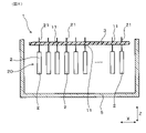
電力変換装置に係る参考形態について、図1~図4を参照して説明する。
本形態の電力変換装置1は、図1、図2に示すごとく、半導体モジュール2と、制御基板3と、電子部品としてのコンデンサ4と、筐体5と、を有する。半導体モジュール2は、スイッチング素子を内蔵している。制御基板3には、半導体モジュール2の信号端子21が接続されている。コンデンサ4は、制御基板3に接続される接続端子41を備えている。筐体5は、半導体モジュール2、制御基板3、及びコンデンサ4を収容している。
( Reference form 1 )
A reference mode relating to the power conversion device will be described with reference to FIGS. 1 to 4.
As shown in FIGS. 1 and 2, the
信号端子21と制御基板3との接続部は、溶着によって接合された溶着接合部11である。
接続端子41と制御基板3との接続部は、コネクタ120によって接続されたコネクタ接続部12である。
コネクタ接続部12は、接続端子41と制御基板3とに、制御基板3の法線方向Zに沿った相対変位を許容する接続部である。
The connection portion between the
The connection portion between the
The
本形態において、溶着接合部11は、はんだ110によって接合されたはんだ接合部である。すなわち、本形態において、図3に示すごとく、溶着接合部11は、信号端子21と制御基板3とに、はんだ110を溶着させることによって、信号端子21と制御基板3とを接合した接合部である。
In this embodiment, the welded
図1、図2に示すごとく、半導体モジュール2とコンデンサ4とは、制御基板3における同じ主面側に配置されている。信号端子21と接続端子41とは、制御基板3の法線方向Zに立設している。以下、制御基板3に対して半導体モジュール2の本体部20及びコンデンサ4の本体部40が配置された側を、下側、その反対側を上側という。ただし、この上下の表現は、便宜的なものであり、特に、電力変換装置1の配置姿勢を限定するものではない。
As shown in FIGS. 1 and 2, the
半導体モジュール2は、複数の信号端子21を、本体部20の上側に突出してなる。複数の信号端子21は、互いに略平行に立設している。信号端子21は、制御基板3に形成されたスルーホール32に挿通されている。そして、信号端子21は、スルーホール32において、制御基板3の配線導体に、はんだ110にて接合されている。
The
半導体モジュール2は、本体部20にIGBT(絶縁ゲートバイポーラトランジスタの略)等のスイッチング素子を内蔵している。そして、複数の信号端子21のうちの一部は、スイッチング素子のゲート等に接続された端子である。また、複数の信号端子21のうちの一部は、例えば、スイッチング素子と共に本体部20に内蔵されたセンサ等に接続されている。なお、図示を省略するが、半導体モジュール2は、信号端子21の他に、パワー端子を突出してなる。
The
本形態において、コンデンサ4は、本体部40から上方へ、接続端子41を1本突出してなる。ただし、接続端子41の本数は特に限定されるものではなく、複数本突出していてもよい。
In the present embodiment, the
コンデンサ4の接続端子41は、例えば、コンデンサ素子と共に本体部40に内蔵された温度センサ、電流センサ等に接続された端子とすることができる。なお、図示を省略するが、コンデンサ4は、接続端子41の他に、コンデンサ素子に接続されたコンデンサ端子を突出してなる。
コンデンサ4は、半導体モジュール2よりも質量が大きい。
The
The
図4に示すごとく、コネクタ120は、制御基板3に実装されている。コネクタ120は、制御基板3の上面に固定されていると共に、制御基板3に形成された配線導体に電気的に接続されている。コネクタ120は、コンデンサ4の接続端子41を挿入するための挿入空間121を、下側に開口させている。挿入空間121は、制御基板3におけるスルーホール34に連通している。
As shown in FIG. 4, the
また、コネクタ120を配置した位置における制御基板3の下面には、ガイド部材13が固定されている。ガイド部材13は、スルーホール34に連通する貫通孔131を有すると共に、貫通孔131の下端においてテーパ状に拡開したガイド面132を有する。接続端子41は、ガイド面132にガイドされながら、スルーホール34に挿通され、コネクタ120の挿入空間121に挿入されるよう構成されている。
Further, the
挿入空間121には、接続端子41に圧接される端子部材122が配置されている。端子部材122が、制御基板3の配線に電気的に接続されている。端子部材122は、接続端子41の挿入方向に直交する方向に弾性変形可能となっている。そして、端子部材122は、コネクタ120の挿入空間121に挿入された接続端子41に、接続端子41の挿入方向に直交する方向から、弾性的に圧接する。
In the
このようにして、接続端子41は、端子部材122に対して、挿入方向、すなわち上下方向に摺動可能に保持されている。つまり、接続端子41は、コネクタ120に対して上下方向に進退可能に保持されている。これにより、コンデンサ4と制御基板3との、制御基板3の法線方向Zにおける相対変位が許容されている。
In this way, the
半導体モジュール2の本体部20及びコンデンサ4の本体部40は、それぞれ、直接的又は間接的に、筐体5に固定されている。半導体モジュール2の本体部20は、例えば図示を省略する冷却器を介して、間接的に筐体5に固定された構成とすることができる。コンデンサ4の本体部40は、例えば、図示を省略する締結部材等によって、筐体5に固定された構成とすることができる。
筐体5は、上方に開口部51を有する。この開口部51は、図示を省略する蓋体によって塞がれる。制御基板3は、筐体5における開口部51付近に配置されている。
The
The
次に、本形態の作用効果につき説明する。
上記電力変換装置1においては、信号端子21と制御基板3との接続部は、溶着接合部11であり、接続端子41と制御基板との接続部は、コネクタ接続部12である。これにより、電力変換装置1において、接続信頼性を確保しつつ、損失を低減することができる。
Next, the action and effect of this embodiment will be described.
In the
まず、接続端子41と制御基板3との接続部は、コネクタ接続部12である。そして、コネクタ接続部12は、接続端子41と制御基板3とに、制御基板3の法線方向Zに沿った相対変位を許容する。これにより、コンデンサ4と制御基板3とは、互いに相対変位が生じても、接続部にかかる負荷を低減できる。それゆえ、コンデンサ4と制御基板3との間の接続信頼性を確保することができる。
First, the connection portion between the
また、これに伴い、コンデンサ4と半導体モジュール2との間の相対変位が生じても、コネクタ接続部12において相対変位が吸収されるため、信号端子21と制御基板3との間の接続部には、負荷がかかりにくい。これにより、信号端子21と制御基板3との間の接続信頼性も確保することができる。
Further, even if a relative displacement occurs between the
そして、信号端子21と制御基板3との接続部は、溶着接合部11である。これにより、信号端子21と制御基板3との間の電気抵抗を小さくすることができる。また、信号端子21の長さを比較的短くすることが可能となる。そのため、半導体モジュール2と制御基板3との間の電流経路を短くすることができ、インダクタンスを低減しやすい。その結果、電力変換装置1の損失を低減することができる。
The connection portion between the
半導体モジュール2とコンデンサ4とは、制御基板3における同じ主面側(すなわち下面側)に配置されており、信号端子21と接続端子41とは、制御基板3の法線方向Zに立設している。これにより、コンデンサ4と制御基板3との間の相対変位及びコンデンサ4と半導体モジュール2との相対変位を、コネクタ接続部12において、より吸収しやすい構成とすることができる。また、筐体5内の省スペース化を図りやすく、電力変換装置1の小型化を図りやすい。
The
また、制御基板3は、溶着接合部11によって半導体モジュール2の複数の信号端子21に固定されている。これにより、半導体モジュール2との接続部分付近において、筐体5に対する制御基板3の固定部を少なくすることも可能となる。その結果、電力変換装置1の小型化、低コスト化を図りやすくなる。
Further, the
以上のごとく、上記態様によれば、接続信頼性を確保しつつ、損失を低減することができる電力変換装置を提供することができる。 As described above, according to the above aspect, it is possible to provide a power conversion device capable of reducing loss while ensuring connection reliability.
(実施形態1)
本実施形態は、図5、図6に示すごとく、制御基板3が、検査用開口部33を、厚み方向に貫通形成してなる。検査用開口部33は、溶着接合部11を視覚的に検査する検査具を挿入することができるよう形成されている。
( Embodiment 1 )
In this embodiment, as shown in FIGS. 5 and 6, the
溶着接合部11は、制御基板3の上側面のみならず、下側面にも形成される。制御基板3の上側面は、目視等によって、容易にその状態を検査することができる。すなわち、溶着接合部11において、例えば、はんだ110(図3参照)の形成状態を、外観検査することがある。かかる場合に、制御基板3の上面側からの検査は容易であっても、下面側からの検査は困難となるおそれがある。例えば、制御基板3が、筐体5の開口面を広い範囲にて覆うような場合には、例えば、ファイバースコープ等の検査具を、制御基板3の外周側から下方へ通すことが困難となる場合がある。特に、電力変換装置1の小型化、構成部品の集積化等に伴い、制御基板3の下面側における溶着接合部11の検査が困難となりやすい。
The welded joint 11 is formed not only on the upper side surface of the
そこで、本形態においては、検査用開口部33を、制御基板3に設けている。特に本形態においては、溶着接合部11の近傍に、検査用開口部33を設けてある。より具体的には、図6に示すごとく、制御基板3の法線方向Zから見て、半導体モジュール2の複数の信号端子21の間となる位置に、検査用開口部33が設けてある。
Therefore, in this embodiment, the inspection opening 33 is provided on the
半導体モジュール2は、複数の信号端子21を、制御基板3の主面に平行な方向に、一列に並べて設けてある。これに対応して、制御基板3には、半導体モジュール2の複数の信号端子21を挿入する複数のスルーホール32を、一列に並べて形成してなる。これらの一列のスルーホール32の配列群は、中央部分に、他の部分よりも間隔の大きい部分を有する。この部分に、検査用開口部33が形成されている。
検査用開口部33の直径は、例えば、スルーホール32の直径よりも大きいものとすることができる。
The
The diameter of the inspection opening 33 may be larger than the diameter of the through
その他の構成は、参考形態1と同様である。なお、実施形態1以降において用いた符号のうち、既出の実施形態において用いた符号と同一のものは、特に示さない限り、既出の実施形態におけるものと同様の構成要素等を表す。
Other configurations are the same as those of
本形態においては、上述のように、制御基板3が検査用開口部33を有するため、溶着接合部11の検査を容易かつ確実に行うことができる。また、検査用開口部33を用いて、溶着接合部11の検査を行うことができるため、筐体5内の部品の配置等の制約が少なくなる。その結果、電力変換装置1の小型化を図りやすくなる。
その他、参考形態1と同様の作用効果を有する。
In this embodiment, as described above, since the
In addition, it has the same effect as that of
(参考形態2)
本形態の電力変換装置1は、図7、図8に示すごとく、制御基板3の主面に沿った方向に複数の半導体モジュール2が積層配置された積層体200を有する。
( Reference form 2 )
As shown in FIGS. 7 and 8, the
本形態において、複数の半導体モジュール2は、同じ姿勢にて、一列に積層配置されている。半導体モジュール2の本体部20は、略直方体形状を有する。そして、半導体モジュール2は、本体部20の最も広い面である一対の主面を積層方向Xに向けて、積層されている。
図示を省略するが、半導体モジュール2は、両主面に配置された冷却管と共に、積層体200を構成することができる。
In this embodiment, the plurality of
Although not shown, the
制御基板3は、図7に示すごとく、法線方向Zから見た形状において、積層体200の積層方向Xにおける長さL1が、積層方向Xに直交する方向における長さL2よりも長い。制御基板3は、法線方向Zから見た形状が、略長方形状であり、その長辺が積層方向Xに沿っている。コンデンサ4は、積層方向Xに長尺な形状を有する。そして、制御基板3の法線方向Zから見て、コンデンサ4は、積層体200に対して、積層方向Xと直交する方向に並んで配置されている。
As shown in FIG. 7, the
コンデンサ4は、接続端子41を複数本有し、これらが、積層方向Xに並んで配置されている。これに対応して、制御基板3には、接続端子41を挿通する複数のスルーホール34を設けている。そして、コネクタ接続部12が複数形成されている。なお、複数のコネクタ接続部12は、複数のコネクタを一体化してなるコネクタモジュール120mにて構成されている。ただし、複数のコネクタ接続部12は、互いに独立した複数のコネクタのそれぞれにて構成してもよい。
The
本形態においては、積層体200を構成する複数の半導体モジュール2の信号端子21に、制御基板3が、溶着接合部11にて接合されることとなる。それゆえ、溶着接合部11の数を多く形成することができる。すなわち、制御基板3の固定点を多くすることができ、制御基板3の耐振性を向上させることができる。そして、これに伴い、筐体5等への制御基板3の締結箇所を少なくすることができる。その結果、電力変換装置1の小型化、低コスト化を図りやすくなる。
In this embodiment, the
また、制御基板3は、積層体200の積層方向Xにおける長さL1が、積層方向Xに直交する方向における長さL2よりも長い。つまり、制御基板3の長手方向に沿って、積層体200が配置されているため、制御基板3の耐振性を向上させやすい。
その他、参考形態1と同様の作用効果を有する。
Further, in the
In addition, it has the same effect as that of
(実施形態2)
本実施形態は、図9、図10に示すごとく、積層体200を有すると共に、制御基板3に検査用開口部33を設けた、電力変換装置1の形態である。
すなわち、参考形態2と同様に、本形態の電力変換装置1は、積層体200を有する。そして、制御基板3には、実施形態1に示したものと同様の検査用開口部33が形成されている。
( Embodiment 2 )
As shown in FIGS. 9 and 10, the present embodiment is a form of the
That is, as in the
本形態においては、図9に示すごとく、制御基板3の法線方向Zから見て、検査用開口部33が、積層方向Xに隣り合う複数の半導体モジュール2の間に配設されている。すなわち、積層方向Xにおいて、隣り合う半導体モジュール2の信号端子21の間に、検査用開口部33が形成されている。換言すると、各半導体モジュール2の複数の信号端子21を挿入する複数のスルーホール32の配列群に対して、積層方向Xにずれた位置に、検査用開口部33が形成されている。
In this embodiment, as shown in FIG. 9, the inspection opening 33 is arranged between the plurality of
法線方向Zから見て、検査用開口部33と半導体モジュール2とは、積層方向Xに交互に配置されている。これに伴い、複数のスルーホール32の配列群と、複数の検査用開口部33とが、積層方向Xに交互に配置されている。
Seen from the normal direction Z, the
また、積層方向Xの端部に配置された半導体モジュール2に対して、積層方向Xの外側となる位置にも、検査用開口部33が形成されている。
その他の構成は、参考形態2と同様である。
Further, an
Other configurations are the same as those of
本形態においては、制御基板3に、複数の検査用開口部33を設けているため、複数の溶着接合部11の検査を容易かつ確実に行うことができる。また、制御基板3の法線方向Zから見て、検査用開口部33が、積層方向Xに隣り合う複数の半導体モジュール2の間に配設されている。これにより、一つの検査用開口部33から、検査具(例えばファイバースコープ等)を挿通して、複数箇所の溶着接合部11の検査を行いやすくなる。
その他、参考形態2と同様の作用効果を有する。
In this embodiment, since the
In addition, it has the same action and effect as
(実施形態3)
本実施形態は、図11に示すごとく、制御基板3に形成した検査用開口部33の数を少なくした形態である。
すなわち、積層方向Xに隣り合う2つの半導体モジュール2に対して、検査用開口部33を1個設けている。つまり、1個の検査用開口部33が、2個の半導体モジュール2に対応するように設けてある。
( Embodiment 3 )
As shown in FIG. 11, the present embodiment is a form in which the number of
That is, one
各検査用開口部33は、制御基板3の法線方向Zから見て、半導体モジュール2の幅方向の中央位置であって、積層方向Xに隣り合う2個の半導体モジュール2の間となる位置に、設けてある。
その他の構成は、参考形態1と同様である。
Each inspection opening 33 is a central position in the width direction of the
Other configurations are the same as those of
本形態においては、検査用開口部33の数を少なくすることで、制御基板3における配線形成領域を確保しやすくなる。その結果、制御基板3の小型化を図りやすくなり、電力変換装置1の小型化を図りやすくなる。また、制御基板3の強度を向上させることができる。
その他、参考形態1と同様の作用効果を有する。
In this embodiment, by reducing the number of
In addition, it has the same effect as that of
(実施形態4)
本実施形態は、図12に示すごとく、制御基板3における検査用開口部33の位置を、半導体モジュール2の複数の信号端子21に対して、コンデンサ4と反対側の位置とした、電力変換装置1の形態である。
( Embodiment 4 )
In this embodiment, as shown in FIG. 12, the power conversion device has the position of the inspection opening 33 in the
積層方向Xに隣り合う2つの半導体モジュール2に対して、検査用開口部33を1個設けている点については、実施形態3と同様である。
その他の構成は、実施形態3と同様である。
It is the same as the third embodiment in that one
Other configurations are the same as those in the third embodiment .
本形態においては、積層体200に対して、幅方向の端部付近に検査用開口部33を設けている。そのため、検査用開口部33の下側に空間が形成されやすい。その結果、検査具を、検査用開口部33から制御基板3の下側へ挿入しやすい。また、半導体モジュール2の複数の信号端子21における溶着接合部11の配列方向の端部付近に検査用開口部33が形成されている。そのため、検査用開口部33から挿入した検査具に対して複数の溶着接合部11が存在する方向が、互いに近くなる。それうえ、検査具によって複数の溶着接合部11を検査しやすい。
その他、参考形態1と同様の作用効果を有する。
In this embodiment, an
In addition, it has the same effect as that of
(実施形態5)
本実施形態は、図13に示すごとく、制御基板3における検査用開口部33の位置を、半導体モジュール2の複数の信号端子21よりも、コンデンサ4に近い側の位置とした、電力変換装置1の形態である。
( Embodiment 5 )
In this embodiment, as shown in FIG. 13, the
積層方向Xに隣り合う2つの半導体モジュール2に対して、検査用開口部33を1個設けている点については、実施形態3及び実施形態4と同様である。
その他の構成は、実施形態3及び実施形態4と同様である。
本形態においても、実施形態4と同様の作用効果を得ることができる。
It is the same as the third and fourth embodiments in that one
Other configurations are the same as those of the third and fourth embodiments .
Also in this embodiment, the same effect as that of the fourth embodiment can be obtained.
上記実施形態においては、電子部品として、コンデンサを設けた形態を示したが、これに限られるものではない。電子部品として、例えば、出力電流や入力電流を検出する電流センサ、電力変換装置と外部インターフェースとの接続を検出するセンサなど、制御基板と接続される種々の電子部品を適用することができる。 In the above embodiment, a capacitor is provided as an electronic component, but the present invention is not limited to this. As the electronic components, various electronic components connected to the control board can be applied, for example, a current sensor for detecting an output current or an input current, a sensor for detecting a connection between a power conversion device and an external interface, and the like.
また、溶着接合部として、はんだを用いた形態を示したが、これに限られず、例えば、ろう付けや、溶接等によって、溶着接合部を構成することもできる。 Further, the form in which solder is used as the welded joint is shown, but the present invention is not limited to this, and the welded joint can also be formed by, for example, brazing, welding, or the like.
本発明は上記各実施形態に限定されるものではなく、その要旨を逸脱しない範囲において種々の実施形態に適用することが可能である。 The present invention is not limited to each of the above embodiments, and can be applied to various embodiments without departing from the gist thereof.
1 電力変換装置
11 溶着接合部
12 コネクタ接続部
2 半導体モジュール
21 信号端子
3 制御基板
4 コンデンサ(電子部品)
41 接続端子
5 筐体
1
41
Claims (6)
上記半導体モジュールの信号端子(21)が接続される制御基板(3)と、
上記制御基板に接続される接続端子(41)を備えた電子部品(4)と、
上記半導体モジュール、上記制御基板、及び上記電子部品を収容した筐体(5)と、を有し、
上記信号端子と上記制御基板との接続部は、溶着によって接合された溶着接合部(11)であり、
上記接続端子と上記制御基板との接続部は、コネクタ(120)によって接続されたコネクタ接続部(12)であり、
上記コネクタ接続部は、上記接続端子と上記制御基板とに、上記制御基板の法線方向(Z)に沿った相対変位を許容する接続部であり、
上記制御基板は、上記溶着接合部を視覚的に検査する検査具を挿入することができる検査用開口部(33)を、厚み方向に貫通形成してなる、電力変換装置(1)。 A semiconductor module (2) with a built-in switching element and
The control board (3) to which the signal terminal (21) of the semiconductor module is connected and
An electronic component (4) provided with a connection terminal (41) connected to the control board, and
It has the semiconductor module, the control board, and the housing (5) containing the electronic components.
The connection portion between the signal terminal and the control board is a welding joint portion (11) joined by welding.
The connection portion between the connection terminal and the control board is a connector connection portion (12) connected by the connector (120).
The connector connection portion is a connection portion that allows relative displacement of the connection terminal and the control board along the normal direction (Z) of the control board .
The control board is a power conversion device (1) in which an inspection opening (33) into which an inspection tool for visually inspecting the welded joint can be inserted is formed through in the thickness direction .
Priority Applications (2)
| Application Number | Priority Date | Filing Date | Title |
|---|---|---|---|
| JP2018026296A JP7047445B2 (en) | 2018-02-16 | 2018-02-16 | Power converter |
| CN201910117497.8A CN110165913B (en) | 2018-02-16 | 2019-02-15 | power conversion device |
Applications Claiming Priority (1)
| Application Number | Priority Date | Filing Date | Title |
|---|---|---|---|
| JP2018026296A JP7047445B2 (en) | 2018-02-16 | 2018-02-16 | Power converter |
Publications (2)
| Publication Number | Publication Date |
|---|---|
| JP2019146307A JP2019146307A (en) | 2019-08-29 |
| JP7047445B2 true JP7047445B2 (en) | 2022-04-05 |
Family
ID=67645379
Family Applications (1)
| Application Number | Title | Priority Date | Filing Date |
|---|---|---|---|
| JP2018026296A Active JP7047445B2 (en) | 2018-02-16 | 2018-02-16 | Power converter |
Country Status (2)
| Country | Link |
|---|---|
| JP (1) | JP7047445B2 (en) |
| CN (1) | CN110165913B (en) |
Citations (8)
| Publication number | Priority date | Publication date | Assignee | Title |
|---|---|---|---|---|
| JP2011015586A (en) | 2009-07-06 | 2011-01-20 | Toyota Motor Corp | Relay connector for inverter device |
| JP2011125083A (en) | 2009-12-08 | 2011-06-23 | Denso Corp | Power converter |
| JP2011258612A (en) | 2010-06-04 | 2011-12-22 | Tdk-Lambda Corp | Circuit board |
| JP2014023268A (en) | 2012-07-18 | 2014-02-03 | Denso Corp | Power conversion device |
| JP2014220916A (en) | 2013-05-08 | 2014-11-20 | 株式会社デンソー | Power conversion device |
| JP2015097452A (en) | 2013-11-15 | 2015-05-21 | 株式会社デンソー | Power converter |
| US20150349661A1 (en) | 2014-06-03 | 2015-12-03 | Cummins Power Generation Ip, Inc. | Modular inverter platform providing physical and electrical configurability and scalability |
| JP2017175807A (en) | 2016-03-24 | 2017-09-28 | サンデン・オートモーティブコンポーネント株式会社 | Electronic circuit device and inverter-integrated electric compressor provided with the same |
Family Cites Families (3)
| Publication number | Priority date | Publication date | Assignee | Title |
|---|---|---|---|---|
| JP5417314B2 (en) * | 2010-12-27 | 2014-02-12 | 日立オートモティブシステムズ株式会社 | Power converter |
| JP5789576B2 (en) * | 2012-09-14 | 2015-10-07 | 日立オートモティブシステムズ株式会社 | Power converter |
| JP6631332B2 (en) * | 2016-03-10 | 2020-01-15 | 株式会社デンソー | Power converter |
-
2018
- 2018-02-16 JP JP2018026296A patent/JP7047445B2/en active Active
-
2019
- 2019-02-15 CN CN201910117497.8A patent/CN110165913B/en active Active
Patent Citations (8)
| Publication number | Priority date | Publication date | Assignee | Title |
|---|---|---|---|---|
| JP2011015586A (en) | 2009-07-06 | 2011-01-20 | Toyota Motor Corp | Relay connector for inverter device |
| JP2011125083A (en) | 2009-12-08 | 2011-06-23 | Denso Corp | Power converter |
| JP2011258612A (en) | 2010-06-04 | 2011-12-22 | Tdk-Lambda Corp | Circuit board |
| JP2014023268A (en) | 2012-07-18 | 2014-02-03 | Denso Corp | Power conversion device |
| JP2014220916A (en) | 2013-05-08 | 2014-11-20 | 株式会社デンソー | Power conversion device |
| JP2015097452A (en) | 2013-11-15 | 2015-05-21 | 株式会社デンソー | Power converter |
| US20150349661A1 (en) | 2014-06-03 | 2015-12-03 | Cummins Power Generation Ip, Inc. | Modular inverter platform providing physical and electrical configurability and scalability |
| JP2017175807A (en) | 2016-03-24 | 2017-09-28 | サンデン・オートモーティブコンポーネント株式会社 | Electronic circuit device and inverter-integrated electric compressor provided with the same |
Also Published As
| Publication number | Publication date |
|---|---|
| JP2019146307A (en) | 2019-08-29 |
| CN110165913B (en) | 2023-08-25 |
| CN110165913A (en) | 2019-08-23 |
Similar Documents
| Publication | Publication Date | Title |
|---|---|---|
| JP4285435B2 (en) | Power converter | |
| JP5429151B2 (en) | Power converter | |
| JP4052205B2 (en) | Power converter | |
| JP6635901B2 (en) | Power converter | |
| US7626256B2 (en) | Compact power semiconductor module having a connecting device | |
| US7847390B2 (en) | Semiconductor device | |
| WO2018066343A1 (en) | Connection module | |
| JP2013229983A (en) | Power conversion device | |
| JP2009087542A (en) | Battery pack and bus bar for battery pack | |
| US20230223605A1 (en) | Battery cell contacting device, and battery module containing such a battery cell contacting device | |
| WO2021020079A1 (en) | Wiring module | |
| US20180233930A1 (en) | Battery monitoring device | |
| EP2838116A1 (en) | Stacked packaging structure | |
| JP6932173B2 (en) | Fixed structure of electronic components and current detector | |
| US20110312213A1 (en) | Flat Cable Wiring Structure | |
| JP7047445B2 (en) | Power converter | |
| KR20100132467A (en) | A power semiconductor module including a method of manufacturing a power semiconductor module and a connection device | |
| US20230125441A1 (en) | Voltage detection line and voltage detection line module | |
| JP7065358B2 (en) | In-vehicle power supply | |
| JP2015179702A (en) | Semiconductor device and manufacturing method thereof | |
| JP2022097920A (en) | Power storage module | |
| JP6307573B1 (en) | Cable fixing structure | |
| JP7614699B2 (en) | Power Conversion Equipment | |
| CN115332731A (en) | Bus bar module | |
| US20250024594A1 (en) | Flexible substrate and bus bar module |
Legal Events
| Date | Code | Title | Description |
|---|---|---|---|
| A621 | Written request for application examination |
Free format text: JAPANESE INTERMEDIATE CODE: A621 Effective date: 20201209 |
|
| A977 | Report on retrieval |
Free format text: JAPANESE INTERMEDIATE CODE: A971007 Effective date: 20211013 |
|
| A131 | Notification of reasons for refusal |
Free format text: JAPANESE INTERMEDIATE CODE: A131 Effective date: 20211026 |
|
| A521 | Request for written amendment filed |
Free format text: JAPANESE INTERMEDIATE CODE: A523 Effective date: 20211210 |
|
| TRDD | Decision of grant or rejection written | ||
| A01 | Written decision to grant a patent or to grant a registration (utility model) |
Free format text: JAPANESE INTERMEDIATE CODE: A01 Effective date: 20220222 |
|
| A61 | First payment of annual fees (during grant procedure) |
Free format text: JAPANESE INTERMEDIATE CODE: A61 Effective date: 20220307 |
|
| R151 | Written notification of patent or utility model registration |
Ref document number: 7047445 Country of ref document: JP Free format text: JAPANESE INTERMEDIATE CODE: R151 |