JP7029007B2 - Display device - Google Patents
Display device Download PDFInfo
- Publication number
- JP7029007B2 JP7029007B2 JP2021027185A JP2021027185A JP7029007B2 JP 7029007 B2 JP7029007 B2 JP 7029007B2 JP 2021027185 A JP2021027185 A JP 2021027185A JP 2021027185 A JP2021027185 A JP 2021027185A JP 7029007 B2 JP7029007 B2 JP 7029007B2
- Authority
- JP
- Japan
- Prior art keywords
- electrode
- layer
- transistor
- substrate
- display device
- Prior art date
- Legal status (The legal status is an assumption and is not a legal conclusion. Google has not performed a legal analysis and makes no representation as to the accuracy of the status listed.)
- Active
Links
Images


Classifications
-
- G—PHYSICS
- G06—COMPUTING; CALCULATING OR COUNTING
- G06F—ELECTRIC DIGITAL DATA PROCESSING
- G06F3/00—Input arrangements for transferring data to be processed into a form capable of being handled by the computer; Output arrangements for transferring data from processing unit to output unit, e.g. interface arrangements
- G06F3/01—Input arrangements or combined input and output arrangements for interaction between user and computer
- G06F3/03—Arrangements for converting the position or the displacement of a member into a coded form
- G06F3/041—Digitisers, e.g. for touch screens or touch pads, characterised by the transducing means
- G06F3/0412—Digitisers structurally integrated in a display
-
- H—ELECTRICITY
- H10—SEMICONDUCTOR DEVICES; ELECTRIC SOLID-STATE DEVICES NOT OTHERWISE PROVIDED FOR
- H10D—INORGANIC ELECTRIC SEMICONDUCTOR DEVICES
- H10D86/00—Integrated devices formed in or on insulating or conducting substrates, e.g. formed in silicon-on-insulator [SOI] substrates or on stainless steel or glass substrates
- H10D86/40—Integrated devices formed in or on insulating or conducting substrates, e.g. formed in silicon-on-insulator [SOI] substrates or on stainless steel or glass substrates characterised by multiple TFTs
-
- G—PHYSICS
- G02—OPTICS
- G02F—OPTICAL DEVICES OR ARRANGEMENTS FOR THE CONTROL OF LIGHT BY MODIFICATION OF THE OPTICAL PROPERTIES OF THE MEDIA OF THE ELEMENTS INVOLVED THEREIN; NON-LINEAR OPTICS; FREQUENCY-CHANGING OF LIGHT; OPTICAL LOGIC ELEMENTS; OPTICAL ANALOGUE/DIGITAL CONVERTERS
- G02F1/00—Devices or arrangements for the control of the intensity, colour, phase, polarisation or direction of light arriving from an independent light source, e.g. switching, gating or modulating; Non-linear optics
- G02F1/01—Devices or arrangements for the control of the intensity, colour, phase, polarisation or direction of light arriving from an independent light source, e.g. switching, gating or modulating; Non-linear optics for the control of the intensity, phase, polarisation or colour
- G02F1/13—Devices or arrangements for the control of the intensity, colour, phase, polarisation or direction of light arriving from an independent light source, e.g. switching, gating or modulating; Non-linear optics for the control of the intensity, phase, polarisation or colour based on liquid crystals, e.g. single liquid crystal display cells
- G02F1/133—Constructional arrangements; Operation of liquid crystal cells; Circuit arrangements
- G02F1/1333—Constructional arrangements; Manufacturing methods
- G02F1/133305—Flexible substrates, e.g. plastics, organic film
-
- G—PHYSICS
- G02—OPTICS
- G02F—OPTICAL DEVICES OR ARRANGEMENTS FOR THE CONTROL OF LIGHT BY MODIFICATION OF THE OPTICAL PROPERTIES OF THE MEDIA OF THE ELEMENTS INVOLVED THEREIN; NON-LINEAR OPTICS; FREQUENCY-CHANGING OF LIGHT; OPTICAL LOGIC ELEMENTS; OPTICAL ANALOGUE/DIGITAL CONVERTERS
- G02F1/00—Devices or arrangements for the control of the intensity, colour, phase, polarisation or direction of light arriving from an independent light source, e.g. switching, gating or modulating; Non-linear optics
- G02F1/01—Devices or arrangements for the control of the intensity, colour, phase, polarisation or direction of light arriving from an independent light source, e.g. switching, gating or modulating; Non-linear optics for the control of the intensity, phase, polarisation or colour
- G02F1/13—Devices or arrangements for the control of the intensity, colour, phase, polarisation or direction of light arriving from an independent light source, e.g. switching, gating or modulating; Non-linear optics for the control of the intensity, phase, polarisation or colour based on liquid crystals, e.g. single liquid crystal display cells
- G02F1/133—Constructional arrangements; Operation of liquid crystal cells; Circuit arrangements
- G02F1/1333—Constructional arrangements; Manufacturing methods
- G02F1/13338—Input devices, e.g. touch panels
-
- G—PHYSICS
- G06—COMPUTING; CALCULATING OR COUNTING
- G06F—ELECTRIC DIGITAL DATA PROCESSING
- G06F3/00—Input arrangements for transferring data to be processed into a form capable of being handled by the computer; Output arrangements for transferring data from processing unit to output unit, e.g. interface arrangements
- G06F3/01—Input arrangements or combined input and output arrangements for interaction between user and computer
- G06F3/03—Arrangements for converting the position or the displacement of a member into a coded form
- G06F3/041—Digitisers, e.g. for touch screens or touch pads, characterised by the transducing means
- G06F3/044—Digitisers, e.g. for touch screens or touch pads, characterised by the transducing means by capacitive means
- G06F3/0445—Digitisers, e.g. for touch screens or touch pads, characterised by the transducing means by capacitive means using two or more layers of sensing electrodes, e.g. using two layers of electrodes separated by a dielectric layer
-
- H—ELECTRICITY
- H10—SEMICONDUCTOR DEVICES; ELECTRIC SOLID-STATE DEVICES NOT OTHERWISE PROVIDED FOR
- H10D—INORGANIC ELECTRIC SEMICONDUCTOR DEVICES
- H10D86/00—Integrated devices formed in or on insulating or conducting substrates, e.g. formed in silicon-on-insulator [SOI] substrates or on stainless steel or glass substrates
- H10D86/40—Integrated devices formed in or on insulating or conducting substrates, e.g. formed in silicon-on-insulator [SOI] substrates or on stainless steel or glass substrates characterised by multiple TFTs
- H10D86/60—Integrated devices formed in or on insulating or conducting substrates, e.g. formed in silicon-on-insulator [SOI] substrates or on stainless steel or glass substrates characterised by multiple TFTs wherein the TFTs are in active matrices
-
- H—ELECTRICITY
- H10—SEMICONDUCTOR DEVICES; ELECTRIC SOLID-STATE DEVICES NOT OTHERWISE PROVIDED FOR
- H10H—INORGANIC LIGHT-EMITTING SEMICONDUCTOR DEVICES HAVING POTENTIAL BARRIERS
- H10H20/00—Individual inorganic light-emitting semiconductor devices having potential barriers, e.g. light-emitting diodes [LED]
- H10H20/80—Constructional details
- H10H20/85—Packages
- H10H20/857—Interconnections, e.g. lead-frames, bond wires or solder balls
-
- H—ELECTRICITY
- H10—SEMICONDUCTOR DEVICES; ELECTRIC SOLID-STATE DEVICES NOT OTHERWISE PROVIDED FOR
- H10K—ORGANIC ELECTRIC SOLID-STATE DEVICES
- H10K50/00—Organic light-emitting devices
- H10K50/80—Constructional details
- H10K50/805—Electrodes
-
- H—ELECTRICITY
- H10—SEMICONDUCTOR DEVICES; ELECTRIC SOLID-STATE DEVICES NOT OTHERWISE PROVIDED FOR
- H10K—ORGANIC ELECTRIC SOLID-STATE DEVICES
- H10K59/00—Integrated devices, or assemblies of multiple devices, comprising at least one organic light-emitting element covered by group H10K50/00
- H10K59/10—OLED displays
- H10K59/12—Active-matrix OLED [AMOLED] displays
- H10K59/123—Connection of the pixel electrodes to the thin film transistors [TFT]
-
- H—ELECTRICITY
- H10—SEMICONDUCTOR DEVICES; ELECTRIC SOLID-STATE DEVICES NOT OTHERWISE PROVIDED FOR
- H10K—ORGANIC ELECTRIC SOLID-STATE DEVICES
- H10K59/00—Integrated devices, or assemblies of multiple devices, comprising at least one organic light-emitting element covered by group H10K50/00
- H10K59/10—OLED displays
- H10K59/12—Active-matrix OLED [AMOLED] displays
- H10K59/131—Interconnections, e.g. wiring lines or terminals
-
- H—ELECTRICITY
- H10—SEMICONDUCTOR DEVICES; ELECTRIC SOLID-STATE DEVICES NOT OTHERWISE PROVIDED FOR
- H10K—ORGANIC ELECTRIC SOLID-STATE DEVICES
- H10K59/00—Integrated devices, or assemblies of multiple devices, comprising at least one organic light-emitting element covered by group H10K50/00
- H10K59/40—OLEDs integrated with touch screens
-
- H—ELECTRICITY
- H10—SEMICONDUCTOR DEVICES; ELECTRIC SOLID-STATE DEVICES NOT OTHERWISE PROVIDED FOR
- H10K—ORGANIC ELECTRIC SOLID-STATE DEVICES
- H10K77/00—Constructional details of devices covered by this subclass and not covered by groups H10K10/80, H10K30/80, H10K50/80 or H10K59/80
- H10K77/10—Substrates, e.g. flexible substrates
- H10K77/111—Flexible substrates
-
- G—PHYSICS
- G02—OPTICS
- G02F—OPTICAL DEVICES OR ARRANGEMENTS FOR THE CONTROL OF LIGHT BY MODIFICATION OF THE OPTICAL PROPERTIES OF THE MEDIA OF THE ELEMENTS INVOLVED THEREIN; NON-LINEAR OPTICS; FREQUENCY-CHANGING OF LIGHT; OPTICAL LOGIC ELEMENTS; OPTICAL ANALOGUE/DIGITAL CONVERTERS
- G02F1/00—Devices or arrangements for the control of the intensity, colour, phase, polarisation or direction of light arriving from an independent light source, e.g. switching, gating or modulating; Non-linear optics
- G02F1/01—Devices or arrangements for the control of the intensity, colour, phase, polarisation or direction of light arriving from an independent light source, e.g. switching, gating or modulating; Non-linear optics for the control of the intensity, phase, polarisation or colour
- G02F1/13—Devices or arrangements for the control of the intensity, colour, phase, polarisation or direction of light arriving from an independent light source, e.g. switching, gating or modulating; Non-linear optics for the control of the intensity, phase, polarisation or colour based on liquid crystals, e.g. single liquid crystal display cells
- G02F1/133—Constructional arrangements; Operation of liquid crystal cells; Circuit arrangements
- G02F1/1333—Constructional arrangements; Manufacturing methods
- G02F1/1345—Conductors connecting electrodes to cell terminals
- G02F1/13458—Terminal pads
-
- G—PHYSICS
- G02—OPTICS
- G02F—OPTICAL DEVICES OR ARRANGEMENTS FOR THE CONTROL OF LIGHT BY MODIFICATION OF THE OPTICAL PROPERTIES OF THE MEDIA OF THE ELEMENTS INVOLVED THEREIN; NON-LINEAR OPTICS; FREQUENCY-CHANGING OF LIGHT; OPTICAL LOGIC ELEMENTS; OPTICAL ANALOGUE/DIGITAL CONVERTERS
- G02F1/00—Devices or arrangements for the control of the intensity, colour, phase, polarisation or direction of light arriving from an independent light source, e.g. switching, gating or modulating; Non-linear optics
- G02F1/01—Devices or arrangements for the control of the intensity, colour, phase, polarisation or direction of light arriving from an independent light source, e.g. switching, gating or modulating; Non-linear optics for the control of the intensity, phase, polarisation or colour
- G02F1/13—Devices or arrangements for the control of the intensity, colour, phase, polarisation or direction of light arriving from an independent light source, e.g. switching, gating or modulating; Non-linear optics for the control of the intensity, phase, polarisation or colour based on liquid crystals, e.g. single liquid crystal display cells
- G02F1/133—Constructional arrangements; Operation of liquid crystal cells; Circuit arrangements
- G02F1/136—Liquid crystal cells structurally associated with a semi-conducting layer or substrate, e.g. cells forming part of an integrated circuit
- G02F1/1362—Active matrix addressed cells
- G02F1/136286—Wiring, e.g. gate line, drain line
- G02F1/13629—Multilayer wirings
-
- G—PHYSICS
- G06—COMPUTING; CALCULATING OR COUNTING
- G06F—ELECTRIC DIGITAL DATA PROCESSING
- G06F2203/00—Indexing scheme relating to G06F3/00 - G06F3/048
- G06F2203/041—Indexing scheme relating to G06F3/041 - G06F3/045
- G06F2203/04103—Manufacturing, i.e. details related to manufacturing processes specially suited for touch sensitive devices
-
- H—ELECTRICITY
- H01—ELECTRIC ELEMENTS
- H01L—SEMICONDUCTOR DEVICES NOT COVERED BY CLASS H10
- H01L2221/00—Processes or apparatus adapted for the manufacture or treatment of semiconductor or solid state devices or of parts thereof covered by H01L21/00
- H01L2221/10—Applying interconnections to be used for carrying current between separate components within a device
- H01L2221/1005—Formation and after-treatment of dielectrics
- H01L2221/101—Forming openings in dielectrics
-
- H—ELECTRICITY
- H01—ELECTRIC ELEMENTS
- H01L—SEMICONDUCTOR DEVICES NOT COVERED BY CLASS H10
- H01L2224/00—Indexing scheme for arrangements for connecting or disconnecting semiconductor or solid-state bodies and methods related thereto as covered by H01L24/00
- H01L2224/80—Methods for connecting semiconductor or other solid state bodies using means for bonding being attached to, or being formed on, the surface to be connected
- H01L2224/83—Methods for connecting semiconductor or other solid state bodies using means for bonding being attached to, or being formed on, the surface to be connected using a layer connector
- H01L2224/838—Bonding techniques
- H01L2224/8385—Bonding techniques using a polymer adhesive, e.g. an adhesive based on silicone, epoxy, polyimide, polyester
- H01L2224/83851—Bonding techniques using a polymer adhesive, e.g. an adhesive based on silicone, epoxy, polyimide, polyester being an anisotropic conductive adhesive
-
- H—ELECTRICITY
- H10—SEMICONDUCTOR DEVICES; ELECTRIC SOLID-STATE DEVICES NOT OTHERWISE PROVIDED FOR
- H10K—ORGANIC ELECTRIC SOLID-STATE DEVICES
- H10K2102/00—Constructional details relating to the organic devices covered by this subclass
- H10K2102/301—Details of OLEDs
- H10K2102/311—Flexible OLED
-
- H—ELECTRICITY
- H10—SEMICONDUCTOR DEVICES; ELECTRIC SOLID-STATE DEVICES NOT OTHERWISE PROVIDED FOR
- H10K—ORGANIC ELECTRIC SOLID-STATE DEVICES
- H10K59/00—Integrated devices, or assemblies of multiple devices, comprising at least one organic light-emitting element covered by group H10K50/00
- H10K59/10—OLED displays
- H10K59/12—Active-matrix OLED [AMOLED] displays
- H10K59/1201—Manufacture or treatment
-
- H—ELECTRICITY
- H10—SEMICONDUCTOR DEVICES; ELECTRIC SOLID-STATE DEVICES NOT OTHERWISE PROVIDED FOR
- H10K—ORGANIC ELECTRIC SOLID-STATE DEVICES
- H10K71/00—Manufacture or treatment specially adapted for the organic devices covered by this subclass
- H10K71/80—Manufacture or treatment specially adapted for the organic devices covered by this subclass using temporary substrates
Landscapes
- Engineering & Computer Science (AREA)
- Physics & Mathematics (AREA)
- Theoretical Computer Science (AREA)
- General Engineering & Computer Science (AREA)
- General Physics & Mathematics (AREA)
- Nonlinear Science (AREA)
- Human Computer Interaction (AREA)
- Microelectronics & Electronic Packaging (AREA)
- Optics & Photonics (AREA)
- Crystallography & Structural Chemistry (AREA)
- Chemical & Material Sciences (AREA)
- Mathematical Physics (AREA)
- Manufacturing & Machinery (AREA)
- Devices For Indicating Variable Information By Combining Individual Elements (AREA)
- Electroluminescent Light Sources (AREA)
- Computer Hardware Design (AREA)
- Electrophonic Musical Instruments (AREA)
- Metal-Oxide And Bipolar Metal-Oxide Semiconductor Integrated Circuits (AREA)
- Electrodes Of Semiconductors (AREA)
- Control Of El Displays (AREA)
- Liquid Crystal (AREA)
Description
本発明の一態様は、表示装置に関する。または、本発明の一態様は、表示装置の作製方法
に関する。
One aspect of the present invention relates to a display device. Alternatively, one aspect of the present invention relates to a method for manufacturing a display device.
なお、本発明の一態様は、上記の技術分野に限定されない。例えば、本発明の一態様は、
物、方法、もしくは製造方法に関する。または、本発明は、プロセス、マシン、マニュフ
ァクチャ、もしくは組成物(コンポジション・オブ・マター)に関する。または、本発明
の一態様は、記憶装置、プロセッサ、それらの駆動方法またはそれらの製造方法に関する
。
It should be noted that one aspect of the present invention is not limited to the above technical fields. For example, one aspect of the present invention is
Regarding goods, methods, or manufacturing methods. Alternatively, the invention relates to a process, machine, manufacture, or composition (composition of matter). Alternatively, one aspect of the present invention relates to a storage device, a processor, a method for driving them, or a method for manufacturing them.
なお、本明細書等において半導体装置とは、半導体特性を利用することで機能しうるもの
全般を指す。よって、トランジスタやダイオードなどの半導体素子や半導体回路は半導体
装置である。また、表示装置、発光装置、照明装置、電気光学装置、及び電子機器などは
、半導体素子や半導体回路を含む場合がある。よって、表示装置、発光装置、照明装置、
電気光学装置、及び電子機器なども半導体装置を有する場合がある。
In the present specification and the like, the semiconductor device refers to all devices that can function by utilizing the semiconductor characteristics. Therefore, semiconductor elements such as transistors and diodes and semiconductor circuits are semiconductor devices. Further, the display device, the light emitting device, the lighting device, the electro-optic device, the electronic device, and the like may include a semiconductor element or a semiconductor circuit. Therefore, display devices, light emitting devices, lighting devices,
Electro-optic devices, electronic devices, and the like may also have semiconductor devices.
近年、表示装置の表示領域に用いる表示素子として、液晶素子の研究開発が盛んに行われ
ている。また、エレクトロルミネッセンス(Electroluminescence:
EL)を利用した発光素子の研究開発も盛んに行われている。発光素子の基本的な構成は
、一対の電極間に発光性の物質を含む層を挟んだものである。この発光素子に電圧を印加
することにより、発光性の物質からの発光が得られる。
In recent years, research and development of liquid crystal elements have been actively carried out as display elements used in the display area of display devices. Also, electroluminescence:
Research and development of light emitting devices using EL) are also being actively carried out. The basic configuration of a light emitting element is that a layer containing a light emitting substance is sandwiched between a pair of electrodes. By applying a voltage to this light emitting element, light emission from a light emitting substance can be obtained.
特に、上述の発光素子は自発光型であるため、これを用いた表示装置は、視認性に優れバ
ックライトが不要であり、消費電力が少ない等の利点を有する。さらに、薄型軽量に作製
でき、応答速度が高いなどの利点も有する。
In particular, since the above-mentioned light emitting element is a self-luminous type, a display device using the above-mentioned light emitting element has advantages such as excellent visibility, no backlight, and low power consumption. Further, it can be manufactured thin and lightweight, and has advantages such as high response speed.
また、上述の表示素子を有する表示装置としては、可撓性が図れることから、可撓性を有
する基板の採用が検討されている。
Further, as a display device having the above-mentioned display element, the adoption of a flexible substrate is being considered because it can be made flexible.
可撓性を有する基板を用いた表示装置の作製方法としては、ガラス基板や石英基板といっ
た基板上に薄膜トランジスタなどの半導体素子を作製した後、例えば該半導体素子と基板
の間に有機樹脂を充填し、ガラス基板や石英基板から他の基板(例えば可撓性を有する基
板)へと半導体素子を転置する技術が開発されている(特許文献1)。
As a method for manufacturing a display device using a flexible substrate, a semiconductor element such as a thin film transistor is manufactured on a substrate such as a glass substrate or a quartz substrate, and then, for example, an organic resin is filled between the semiconductor element and the substrate. , A technique for transferring a semiconductor element from a glass substrate or a quartz substrate to another substrate (for example, a flexible substrate) has been developed (Patent Document 1).
可撓性を有する基板上に形成された発光素子は、発光素子表面の保護や外部からの水分や
不純物の浸入を防ぐため、発光素子上にさらに可撓性を有する基板を設けることがある。
For the light emitting element formed on the flexible substrate, a more flexible substrate may be provided on the light emitting element in order to protect the surface of the light emitting element and prevent the infiltration of moisture and impurities from the outside.
また、表示装置は様々な用途への応用が期待されており、多様化が求められている。例え
ば、携帯情報端末として、タッチセンサを備えるスマートフォンやタブレット端末の開発
が進められている。
In addition, display devices are expected to be applied to various applications, and diversification is required. For example, as mobile information terminals, smartphones and tablet terminals equipped with touch sensors are being developed.
可撓性を有する基板を用いた表示装置へ信号や電力を供給するためには、可撓性を有する
基板の一部をレーザー光や刃物を用いて除去して電極を露出させ、FPC(Flexib
le printed circuit)等の外部電極を接続する必要がある。
In order to supply a signal or electric power to a display device using a flexible substrate, a part of the flexible substrate is removed by using a laser beam or a blade to expose an electrode, and FPC (Flexib) is used.
It is necessary to connect an external electrode such as a printed circuit).
しかしながら、可撓性を有する基板の一部をレーザー光や刃物を用いて除去する方法では
、表示装置が有する電極にダメージを与えやすく、表示装置の信頼性や作製歩留まりが低
下しやすいという問題がある。また、上記方法による表示領域へのダメージを防ぐため、
表示領域と電極を十分に離して設置する必要があり、配線抵抗の増加による信号や電力の
減衰が生じやすい。
However, the method of removing a part of the flexible substrate by using a laser beam or a blade tends to damage the electrodes of the display device, and there is a problem that the reliability of the display device and the manufacturing yield tend to decrease. be. In addition, in order to prevent damage to the display area by the above method,
It is necessary to install the display area and the electrodes sufficiently apart from each other, and the signal and power are likely to be attenuated due to the increase in wiring resistance.
本発明の一態様は、電極にダメージを与えにくい表示装置の作製方法を提供することを課
題の一つとする。または、本発明の一態様は、表示領域にダメージを与えにくい表示装置
の作製方法を提供することを課題の一つとする。または、本発明の一態様は、信頼性の良
好な表示装置及びその作製方法を提供することを課題の一つとする。または、本発明の一
態様は、設計の自由度が高い表示装置及びその作製方法を提供することを課題の一つとす
る。
One of the problems of the present invention is to provide a method for manufacturing a display device that does not easily damage the electrodes. Alternatively, one aspect of the present invention is to provide a method for manufacturing a display device that does not easily damage the display area. Alternatively, one aspect of the present invention is to provide a highly reliable display device and a method for manufacturing the display device. Alternatively, one aspect of the present invention is to provide a display device having a high degree of freedom in design and a method for manufacturing the display device.
または、本発明の一態様は、視認性に優れた表示装置、もしくは電子機器などを提供する
ことを課題の一つとする。または、本発明の一態様は、表示品位が良好な表示装置、もし
くは電子機器などを提供することを課題の一つとする。または、本発明の一態様は、信頼
性が高い表示装置、もしくは電子機器などを提供することを課題の一つとする。または、
本発明の一態様は、破損しにくい表示装置、もしくは電子機器などを提供することを課題
の一つとする。または、本発明の一態様は、消費電力が低い表示装置、もしくは電子機器
などを提供することを課題の一つとする。または、本発明の一態様は、生産性が高い表示
装置、もしくは電子機器などを提供することを課題の一つとする。または、本発明の一態
様は、新規な表示装置、もしくは電子機器などを提供することを課題の一つとする。
Alternatively, one aspect of the present invention is to provide a display device, an electronic device, or the like having excellent visibility. Alternatively, one aspect of the present invention is to provide a display device, an electronic device, or the like having good display quality. Alternatively, one aspect of the present invention is to provide a highly reliable display device, electronic device, or the like. or,
One aspect of the present invention is to provide a display device, an electronic device, or the like that is not easily damaged. Alternatively, one aspect of the present invention is to provide a display device, an electronic device, or the like having low power consumption. Alternatively, one aspect of the present invention is to provide a display device, an electronic device, or the like with high productivity. Alternatively, one aspect of the present invention is to provide a new display device, an electronic device, or the like.
なお、これらの課題の記載は、他の課題の存在を妨げるものではない。なお、本発明の一
態様は、これらの課題の全てを解決する必要はないものとする。なお、これら以外の課題
は、明細書、図面、請求項などの記載から、自ずと明らかとなるものであり、明細書、図
面、請求項などの記載から、これら以外の課題を抽出することが可能である。
The description of these issues does not preclude the existence of other issues. It should be noted that one aspect of the present invention does not need to solve all of these problems. Issues other than these are self-evident from the description of the description, drawings, claims, etc., and it is possible to extract problems other than these from the description of the specification, drawings, claims, etc. Is.
本発明の一態様は、可撓性を有する2つの基板に挟まれた表示素子とタッチセンサを有し
、表示素子に信号を供給する外部電極と、タッチセンサに信号を供給する外部電極が一方
の基板の同一面側から接続する表示装置である。
In one aspect of the present invention, there is an external electrode that has a display element and a touch sensor sandwiched between two flexible substrates and supplies a signal to the display element, and an external electrode that supplies a signal to the touch sensor. It is a display device connected from the same side of the board.
本発明の一態様は、第1の基板と、第2の基板と、表示素子と、タッチセンサと、第1の
電極と、第2の電極と、を有し、第1の基板と、第2の基板は、表示素子、タッチセンサ
、第1の電極、及び第2の電極を挟んで、互いに重なる領域を有し、第1の電極は表示素
子に信号を供給することができる機能を有し、第2の電極はタッチセンサに信号を供給す
ることができる機能を有し、第1の電極と第2の電極は、第2の基板が有する開口におい
て、外部電極と電気的に接続されている表示装置である。
One aspect of the present invention includes a first substrate, a second substrate, a display element, a touch sensor, a first electrode, a second electrode, a first substrate, and a first. The
外部電極としては、FPC等を用いることができる。また、外部電極は複数の電極を有し
、第1の電極は外部電極が有する電極の一部と電気的に接続することができる。また、第
2の電極は外部電極が有する電極の他の一部と電気的に接続することができる。また、第
1の電極と第2の電極に共通の電位または共通の信号を供給する場合は、第1の電極と第
2の電極を、外部電極が有する1つの電極と電気的に接続することもできる。
As the external electrode, FPC or the like can be used. Further, the external electrode has a plurality of electrodes, and the first electrode can be electrically connected to a part of the electrodes of the external electrode. Further, the second electrode can be electrically connected to another part of the electrode of the external electrode. Further, when supplying a common potential or a common signal to the first electrode and the second electrode, the first electrode and the second electrode are electrically connected to one electrode of the external electrode. You can also.
または、本発明の一態様は、第1の基板と、第2の基板と、表示素子と、タッチセンサと
、第1の電極と、第2の電極と、を有し、第1の基板と、第2の基板は、表示素子、タッ
チセンサ、第1の電極、及び第2の電極を挟んで、互いに重なる領域を有し、第1の電極
は表示素子に信号を供給することができる機能を有し、第2の電極はタッチセンサに信号
を供給することができる機能を有し、第1の電極は、第2の基板が有する第1の開口にお
いて第1の外部電極と電気的に接続し、第2の電極は、第2の基板が有する第2の開口に
おいて第2の外部電極と電気的に接続されている表示装置である。
Alternatively, one aspect of the present invention includes a first substrate, a second substrate, a display element, a touch sensor, a first electrode, a second electrode, and the first substrate. , The second substrate has a region overlapping the display element, the touch sensor, the first electrode, and the second electrode, and the first electrode has a function of supplying a signal to the display element. The second electrode has a function of being able to supply a signal to the touch sensor, and the first electrode is electrically with the first external electrode in the first opening of the second substrate. The second electrode connected is a display device that is electrically connected to the second external electrode at the second opening of the second substrate.
または、本発明の一態様は、第1の基板と、第2の基板と、表示素子と、タッチセンサと
、トランジスタと、第1の電極と、第2の電極と、を有し、第1の基板と第2の基板は、
表示素子、タッチセンサ、トランジスタ、第1の電極、及び第2の電極を挟んで、互いに
重なる領域を有し、第1の電極はトランジスタに信号を供給することができる機能を有し
、トランジスタは表示素子に信号を供給することができる機能を有し、第2の電極はタッ
チセンサに信号を供給することができる機能を有し、第1の電極と第2の電極は、第2の
基板が有する開口において、外部電極と電気的に接続されている表示装置である。
Alternatively, one aspect of the present invention includes a first substrate, a second substrate, a display element, a touch sensor, a transistor, a first electrode, and a second electrode, and the first aspect thereof. The board and the second board are
The display element, the touch sensor, the transistor, the first electrode, and the second electrode are sandwiched between them, and the region overlaps with each other. The first electrode has a function of supplying a signal to the transistor, and the transistor has a function. The second electrode has a function of supplying a signal to the display element, the second electrode has a function of supplying a signal to the touch sensor, and the first electrode and the second electrode are the second substrate. It is a display device that is electrically connected to an external electrode at the opening of the.
または、本発明の一態様は、第1の基板と、第2の基板と、表示素子と、タッチセンサと
、トランジスタと、第1の電極と、第2の電極と、を有し、第1の基板と、第2の基板は
、表示素子、タッチセンサ、第1の電極、及び第2の電極を挟んで、互いに重なる領域を
有し、第1の電極はトランジスタに信号を供給することができる機能を有し、トランジス
タは表示素子に信号を供給することができる機能を有し、第2の電極はタッチセンサに信
号を供給することができる機能を有し、第1の電極は第2の基板が有する第1の開口にお
いて第1の外部電極と電気的に接続し、第2の電極は第2の基板が有する第2の開口にお
いて第2の外部電極と電気的に接続されている表示装置である。
Alternatively, one aspect of the present invention includes a first substrate, a second substrate, a display element, a touch sensor, a transistor, a first electrode, and a second electrode, and the first aspect thereof. The substrate and the second substrate have regions that overlap each other with the display element, the touch sensor, the first electrode, and the second electrode interposed therebetween, and the first electrode can supply a signal to the transistor. The transistor has a function of being able to supply a signal to the display element, the second electrode has a function of being able to supply a signal to the touch sensor, and the first electrode has a function of being able to supply a signal. The second electrode is electrically connected to the first external electrode at the first opening of the substrate, and the second electrode is electrically connected to the second external electrode at the second opening of the second substrate. It is a display device.
本発明の一態様によれば、電極にダメージを与えにくい表示装置の作製方法を提供するこ
とができる。または、本発明の一態様によれば、表示領域にダメージを与えにくい表示装
置の作製方法を提供することができる。または、本発明の一態様によれば、信頼性の良好
な表示装置及びその作製方法を提供することができる。または、本発明の一態様によれば
、設計の自由度が高い表示装置及びその作製方法を提供することができる。
According to one aspect of the present invention, it is possible to provide a method for manufacturing a display device that does not easily damage the electrodes. Alternatively, according to one aspect of the present invention, it is possible to provide a method for manufacturing a display device that does not easily damage the display area. Alternatively, according to one aspect of the present invention, it is possible to provide a display device having good reliability and a method for manufacturing the same. Alternatively, according to one aspect of the present invention, it is possible to provide a display device having a high degree of freedom in design and a method for manufacturing the display device.
または、本発明の一態様は、視認性に優れた表示装置、もしくは電子機器などを提供する
ことができる。または、本発明の一態様は、表示品位が良好な表示装置、もしくは電子機
器などを提供することができる。または、本発明の一態様は、信頼性が高い表示装置、も
しくは電子機器などを提供することができる。または、本発明の一態様は、破損しにくい
表示装置、もしくは電子機器などを提供することができる。または、発明の一態様は、消
費電力が低い表示装置、もしくは電子機器などを提供することができる。または、発明の
一態様は、生産性が高い表示装置、もしくは電子機器などを提供することができる。また
は、本発明の一態様は、新規な表示装置、もしくは電子機器などを提供することを提供す
ることができる。
Alternatively, one aspect of the present invention can provide a display device, an electronic device, or the like having excellent visibility. Alternatively, one aspect of the present invention can provide a display device, an electronic device, or the like having good display quality. Alternatively, one aspect of the present invention can provide a highly reliable display device, electronic device, or the like. Alternatively, one aspect of the present invention can provide a display device, an electronic device, or the like that is not easily damaged. Alternatively, one aspect of the invention can provide a display device, an electronic device, or the like having low power consumption. Alternatively, one aspect of the invention can provide a highly productive display device, electronic device, or the like. Alternatively, one aspect of the present invention can provide a new display device, an electronic device, or the like.
なお、これらの効果の記載は、他の効果の存在を妨げるものではない。なお、本発明の一
態様は、これらの効果の全てを有する必要はない。なお、これら以外の効果は、明細書、
図面、請求項などの記載から、自ずと明らかとなるものであり、明細書、図面、請求項な
どの記載から、これら以外の効果を抽出することが可能である。
The description of these effects does not preclude the existence of other effects. It should be noted that one aspect of the present invention does not have to have all of these effects. In addition, the effects other than these are described in the specification.
It is self-evident from the description of the drawings, claims, etc., and it is possible to extract effects other than these from the description of the specification, drawings, claims, etc.
実施の形態について、図面を用いて詳細に説明する。但し、本発明は以下の説明に限定さ
れず、本発明の趣旨及びその範囲から逸脱することなくその形態及び詳細を様々に変更し
得ることは当業者であれば容易に理解される。従って、本発明は以下に示す実施の形態の
記載内容に限定して解釈されるものではない。なお、以下に説明する発明の構成において
、同一部分又は同様な機能を有する部分には同一の符号を異なる図面間で共通して用い、
その繰り返しの説明は省略する。
The embodiments will be described in detail with reference to the drawings. However, the present invention is not limited to the following description, and it is easily understood by those skilled in the art that the form and details of the present invention can be variously changed without departing from the spirit and scope of the present invention. Therefore, the present invention is not construed as being limited to the description of the embodiments shown below. In the configuration of the invention described below, the same reference numerals are commonly used between different drawings for the same parts or parts having similar functions.
The explanation of the repetition will be omitted.
また、図面等において示す各構成の、位置、大きさ、範囲などは、発明の理解を容易とす
るため、実際の位置、大きさ、範囲などを表していない場合がある。このため、開示する
発明は、必ずしも、図面等に開示された位置、大きさ、範囲などに限定されない。例えば
、実際の製造工程において、エッチングなどの処理によりレジストマスクなどが意図せず
に目減りすることがあるが、理解を容易とするために省略して示すことがある。
In addition, the position, size, range, etc. of each configuration shown in the drawings and the like may not represent the actual position, size, range, etc. in order to facilitate understanding of the invention. Therefore, the disclosed invention is not necessarily limited to the position, size, range, etc. disclosed in the drawings and the like. For example, in an actual manufacturing process, a resist mask or the like may be unintentionally reduced due to a process such as etching, but it may be omitted for ease of understanding.
また、上面図(「平面図」ともいう)や斜視図などにおいて、図面をわかりやすくするた
めに、一部の構成要素の記載を省略する場合がある。
Further, in the top view (also referred to as “plan view”) or the perspective view, the description of some components may be omitted in order to make the drawing easier to understand.
また、本明細書等において「電極」や「配線」の用語は、これらの構成要素を機能的に限
定するものではない。例えば、「電極」は「配線」の一部として用いられることがあり、
その逆もまた同様である。さらに、「電極」や「配線」の用語は、複数の「電極」や「配
線」が一体となって形成されている場合なども含む。
Further, in the present specification and the like, the terms "electrode" and "wiring" do not functionally limit these components. For example, an "electrode" may be used as part of a "wiring",
The reverse is also true. Further, the terms "electrode" and "wiring" include the case where a plurality of "electrodes" and "wiring" are integrally formed.
なお、本明細書等において「上」や「下」の用語は、構成要素の位置関係が直上または直
下で、かつ、直接接していることを限定するものではない。例えば、「絶縁層A上の電極
B」の表現であれば、絶縁層Aの上に電極Bが直接接して形成されている必要はなく、絶
縁層Aと電極Bとの間に他の構成要素を含むものを除外しない。
In the present specification and the like, the terms "upper" and "lower" do not limit the positional relationship of the components to be directly above or directly below and to be in direct contact with each other. For example, in the case of the expression "electrode B on the insulating layer A", it is not necessary that the electrode B is formed in direct contact with the insulating layer A, and another configuration is formed between the insulating layer A and the electrode B. Do not exclude those that contain elements.
また、ソース及びドレインの機能は、異なる極性のトランジスタを採用する場合や、回路
動作において電流の方向が変化する場合など、動作条件などによって互いに入れ替わるた
め、いずれがソースまたはドレインであるかを限定することが困難である。このため、本
明細書においては、ソース及びドレインの用語は、入れ替えて用いることができるものと
する。
In addition, the functions of the source and drain are interchanged depending on the operating conditions, such as when transistors with different polarities are adopted or when the direction of the current changes in the circuit operation, so which one is the source or drain is limited. Is difficult. Therefore, in the present specification, the terms source and drain can be used interchangeably.
また、本明細書等において、「電気的に接続」には、「何らかの電気的作用を有するもの
」を介して接続されている場合が含まれる。ここで、「何らかの電気的作用を有するもの
」は、接続対象間での電気信号の授受を可能とするものであれば、特に制限を受けない。
よって、「電気的に接続する」と表現される場合であっても、現実の回路においては、物
理的な接続部分がなく、配線が延在しているだけの場合もある。
Further, in the present specification and the like, "electrically connected" includes the case of being connected via "something having some kind of electrical action". Here, the "thing having some kind of electrical action" is not particularly limited as long as it enables the exchange of electric signals between the connection targets.
Therefore, even when it is expressed as "electrically connected", in an actual circuit, there is a case where there is no physical connection portion and only the wiring is extended.
また、本明細書において、「平行」とは、二つの直線が-10°以上10°以下の角度で
配置されている状態をいう。従って、-5°以上5°以下の場合も含まれる。また、「垂
直」及び「直交」とは、二つの直線が80°以上100°以下の角度で配置されている状
態をいう。従って、85°以上95°以下の場合も含まれる。
Further, in the present specification, "parallel" means a state in which two straight lines are arranged at an angle of −10 ° or more and 10 ° or less. Therefore, the case of −5 ° or more and 5 ° or less is also included. Further, "vertical" and "orthogonal" mean a state in which two straight lines are arranged at an angle of 80 ° or more and 100 ° or less. Therefore, the case of 85 ° or more and 95 ° or less is also included.
また、本明細書において、リソグラフィ工程を行った後にエッチング工程を行う場合は、
特段の説明がない限り、リソグラフィ工程で形成したレジストマスクは、エッチング工程
終了後に除去するものとする。
Further, in the present specification, when the etching process is performed after the lithography process is performed,
Unless otherwise specified, the resist mask formed in the lithography process shall be removed after the etching process is completed.
また、電圧は、ある電位と、基準の電位(例えば接地電位(GND電位)またはソース電
位)との電位差のことを示す場合が多い。よって、電圧を電位と言い換えることが可能で
ある。
Further, the voltage often indicates a potential difference between a certain potential and a reference potential (for example, a ground potential (GND potential) or a source potential). Therefore, it is possible to paraphrase voltage as electric potential.
なお、半導体の不純物とは、例えば、半導体を構成する主成分以外をいう。例えば、濃度
が0.1原子%未満の元素は不純物と言える。不純物が含まれることにより、例えば、半
導体のDOS(Density of State)が高くなることや、キャリア移動度
が低下することや、結晶性が低下することなどが起こる場合がある。半導体が酸化物半導
体である場合、半導体の特性を変化させる不純物としては、例えば、第1族元素、第2族
元素、第13族元素、第14族元素、第15族元素、および酸化物半導体の主成分以外の
遷移金属などがあり、特に、例えば、水素(水にも含まれる)、リチウム、ナトリウム、
シリコン、ホウ素、リン、炭素、窒素などがある。酸化物半導体の場合、例えば水素など
の不純物の混入によって酸素欠損を形成する場合がある。また、半導体がシリコンである
場合、半導体の特性を変化させる不純物としては、例えば、酸素、水素を除く第1族元素
、第2族元素、第13族元素、第15族元素などがある。
The semiconductor impurities are, for example, other than the main components constituting the semiconductor. For example, an element having a concentration of less than 0.1 atomic% can be said to be an impurity. The inclusion of impurities may result in, for example, an increase in the DOS (Density of State) of the semiconductor, a decrease in carrier mobility, a decrease in crystallinity, and the like. When the semiconductor is an oxide semiconductor, the impurities that change the characteristics of the semiconductor include, for example,
There are silicon, boron, phosphorus, carbon, nitrogen and so on. In the case of oxide semiconductors, oxygen deficiency may be formed by mixing impurities such as hydrogen. When the semiconductor is silicon, the impurities that change the characteristics of the semiconductor include, for example,
なお、本明細書等における「第1」、「第2」等の序数詞は、構成要素の混同を避けるた
めに付すものであり、工程順または積層順など、なんらかの順番や順位を示すものではな
い。また、本明細書等において序数詞が付されていない用語であっても、構成要素の混同
を避けるため、特許請求の範囲において序数詞が付される場合がある。また、本明細書等
において序数詞が付されている用語であっても、特許請求の範囲において異なる序数詞が
付される場合がある。また、本明細書等において序数詞が付されている用語であっても、
特許請求の範囲などにおいて序数詞を省略する場合がある。
The ordinal numbers such as "first" and "second" in the present specification and the like are added to avoid confusion of the components, and do not indicate any order or order such as process order or stacking order. .. In addition, even terms that do not have ordinal numbers in the present specification and the like may be given ordinal numbers within the scope of the claims in order to avoid confusion of the components. Further, even if the terms have ordinal numbers in the present specification and the like, different ordinal numbers may be added within the scope of the claims. In addition, even if the terms have ordinal numbers in the present specification and the like,
Ordinal numbers may be omitted in the claims.
なお、「チャネル長」とは、例えば、トランジスタの上面図において、半導体(またはト
ランジスタがオン状態のときに半導体の中で電流の流れる部分)とゲート電極とが重なる
領域、またはチャネルが形成される領域における、ソース(ソース領域またはソース電極
)とドレイン(ドレイン領域またはドレイン電極)との間の距離をいう。なお、一つのト
ランジスタにおいて、チャネル長が全ての領域で同じ値をとるとは限らない。すなわち、
一つのトランジスタのチャネル長は、一つの値に定まらない場合がある。そのため、本明
細書では、チャネル長は、チャネルの形成される領域における、いずれか一の値、最大値
、最小値または平均値とする。
The "channel length" is, for example, in the top view of the transistor, a region or channel where the semiconductor (or the part where the current flows in the semiconductor when the transistor is on) and the gate electrode overlap is formed. The distance between the source (source region or source electrode) and the drain (drain region or drain electrode) in the region. In one transistor, the channel length does not always take the same value in all regions. That is,
The channel length of one transistor may not be fixed to one value. Therefore, in the present specification, the channel length is any one value, the maximum value, the minimum value, or the average value in the region where the channel is formed.
また、「チャネル幅」とは、例えば、半導体(またはトランジスタがオン状態のときに半
導体の中で電流の流れる部分)とゲート電極とが重なる領域、またはチャネルが形成され
る領域における、ソースとドレインとが向かい合っている部分の長さをいう。なお、一つ
のトランジスタにおいて、チャネル幅がすべての領域で同じ値をとるとは限らない。すな
わち、一つのトランジスタのチャネル幅は、一つの値に定まらない場合がある。そのため
、本明細書では、チャネル幅は、チャネルの形成される領域における、いずれか一の値、
最大値、最小値または平均値とする。
Further, the "channel width" is, for example, a source and a drain in a region where a semiconductor (or a portion where a current flows in the semiconductor when the transistor is on) and a gate electrode overlap, or a region where a channel is formed. The length of the part facing each other. In one transistor, the channel width does not always take the same value in all regions. That is, the channel width of one transistor may not be fixed to one value. Therefore, in the present specification, the channel width is a value of any one in the region where the channel is formed.
The maximum value, the minimum value, or the average value.
なお、トランジスタの構造によっては、実際にチャネルの形成される領域におけるチャネ
ル幅(以下、実効的なチャネル幅と呼ぶ)と、トランジスタの上面図において示されるチ
ャネル幅(以下、見かけ上のチャネル幅と呼ぶ)と、が異なる場合がある。例えば、ゲー
ト電極が半導体の側面を覆う場合、実効的なチャネル幅が、見かけ上のチャネル幅よりも
大きくなり、その影響が無視できなくなる場合がある。例えば、微細かつゲート電極が半
導体の側面を覆うトランジスタでは、半導体の上面に形成されるチャネル領域の割合に対
して、半導体の側面に形成されるチャネル領域の割合が大きくなる場合がある。その場合
は、見かけ上のチャネル幅よりも、実効的なチャネル幅の方が大きくなる。
Depending on the structure of the transistor, the channel width in the region where the channel is actually formed (hereinafter referred to as the effective channel width) and the channel width shown in the top view of the transistor (hereinafter referred to as the apparent channel width). Call) and may be different. For example, when the gate electrode covers the side surface of the semiconductor, the effective channel width may be larger than the apparent channel width, and the influence thereof may not be negligible. For example, in a transistor that is fine and has a gate electrode covering the side surface of the semiconductor, the ratio of the channel region formed on the side surface of the semiconductor may be larger than the ratio of the channel region formed on the upper surface of the semiconductor. In that case, the effective channel width is larger than the apparent channel width.
このような場合、実効的なチャネル幅の、実測による見積もりが困難となる場合がある。
例えば、設計値から実効的なチャネル幅を見積もるためには、半導体の形状が既知という
仮定が必要である。したがって、半導体の形状が正確にわからない場合には、実効的なチ
ャネル幅を正確に測定することは困難である。
In such a case, it may be difficult to estimate the effective channel width by actual measurement.
For example, in order to estimate the effective channel width from the design value, it is necessary to assume that the shape of the semiconductor is known. Therefore, if the shape of the semiconductor is not known accurately, it is difficult to accurately measure the effective channel width.
そこで、本明細書では、見かけ上のチャネル幅を、「囲い込みチャネル幅(SCW:Su
rrounded Channel Width)」と呼ぶ場合がある。また、本明細書
では、単にチャネル幅と記載した場合には、囲い込みチャネル幅または見かけ上のチャネ
ル幅を指す場合がある。または、本明細書では、単にチャネル幅と記載した場合には、実
効的なチャネル幅を指す場合がある。なお、チャネル長、チャネル幅、実効的なチャネル
幅、見かけ上のチャネル幅、囲い込みチャネル幅などは、断面TEM像などを解析するこ
となどによって、値を決定することができる。
Therefore, in the present specification, the apparent channel width is referred to as “enclosure channel width (SCW: Su”).
It may be called "rounded Channel Withth)". Further, in the present specification, when simply described as a channel width, it may refer to an enclosed channel width or an apparent channel width. Alternatively, in the present specification, the term "channel width" may refer to an effective channel width. The values of the channel length, channel width, effective channel width, apparent channel width, enclosed channel width, and the like can be determined by analyzing a cross-sectional TEM image or the like.
なお、トランジスタの電界効果移動度や、チャネル幅当たりの電流値などを計算して求め
る場合、囲い込みチャネル幅を用いて計算する場合がある。その場合には、実効的なチャ
ネル幅を用いて計算する場合とは異なる値をとる場合がある。
When calculating the electric field effect mobility of the transistor, the current value per channel width, or the like, the enclosed channel width may be used for calculation. In that case, the value may be different from the case calculated using the effective channel width.
(実施の形態1)
本発明の一態様の表示装置100の構成例及び作製方法例について、図1乃至図19を用
いて説明する。なお、本明細書に開示する表示装置100は、表示素子として発光素子を
用いた表示装置を例示する。また、本発明の一態様の表示装置100として、トップエミ
ッション構造(上面射出構造)の表示装置を例示する。表示装置100をボトムエミッシ
ョン構造(下面射出構造)、またはデュアルエミッション構造(両面射出構造)の表示装
置とすることも可能である。
(Embodiment 1)
A configuration example and a manufacturing method example of the
<表示装置の構成>
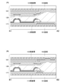
本発明の一態様の表示装置100の構成例について、図1乃至図3を用いて説明する。図
1(A)は、表示装置100の斜視図である。また、図1(B)は、図1(A)にA1-
A2の一点鎖線で示す部位の断面図である。また、図1(C)は、図1(A)にB1-B
2の一点鎖線で示す部位の断面図である。本実施の形態に示す表示装置100は、表示領
域131を有する。また、表示領域131は、複数の画素130を有する。一つの画素1
30は、少なくとも一つの発光素子125を有する。
<Display device configuration>
A configuration example of the
It is sectional drawing of the part shown by the alternate long and short dash line of A2. Further, FIG. 1 (C) shows B1-B in FIG. 1 (A).
It is sectional drawing of the part shown by the one-dot chain line of 2. The
30 has at least one
本実施の形態に示す表示装置100は、電極115、EL層117、及び電極118を含
む発光素子125、隔壁114、及び電極116を有する。また、電極116上に絶縁層
141を有し、絶縁層141に設けられた開口において、電極115と電極116が電気
的に接続されている。また、隔壁114は電極115上に設けられ、電極115及び隔壁
114上にEL層117が設けられ、EL層117上に電極118が設けられている。
The
また、本実施の形態に示す表示装置100は、発光素子125上に接着層120を介して
基板121を有する。また、基板121は、接着層122及び絶縁層129を介して、電
極272、絶縁層273、及び電極274を含むタッチセンサ271、電極276、絶縁
層275、遮光層264、着色層(「カラーフィルタ」ともいう)266、及びオーバー
コート層268を有している。本実施の形態では、タッチセンサ271として静電容量方
式のタッチセンサを例示している。
Further, the
本実施の形態に示す表示装置100は、トップエミッション構造(上面射出構造)の表示
装置であるため、発光素子125から射出された光151は、基板121側から射出され
る。EL層117から射出された光151(例えば、白色光)は、着色層266透過時に
その一部が吸収されて、特定の色の光に変換される。換言すると、着色層266は、特定
の波長帯域の光を透過する。着色層266は、光151を異なる色の光に変換するための
光学フィルター層として機能できる。
Since the
また、本実施の形態では、電極116を電極116aと電極116bの積層として示して
いるが、電極116は単層でもよいし3層以上の積層としてもよい。また、電極276を
電極276aと電極276bの積層として示しているが、電極276は単層でもよいし3
層以上の積層としてもよい。
Further, in the present embodiment, the
It may be laminated with more than one layer.
また、本実施の形態に示す表示装置100は、基板121、接着層122、絶縁層129
、接着層120、絶縁層273、絶縁層275、及び絶縁層141を貫通し、電極116
と重なる開口132aを有する。また、基板121、接着層122、及び絶縁層129を
貫通し、電極276と重なる開口132bを有する。
Further, the
The
Has an
開口132aにおいて、外部電極124aと電極116が、異方性導電接続層138aを
介して電気的に接続されている。また、開口132bにおいて、外部電極124bと電極
276が、異方性導電接続層138bを介して電気的に接続されている。
In the
なお、図2に示すように、表示装置100の構成を、遮光層264、着色層266、及び
オーバーコート層268を有さない構成とすることもできる。図2(A)は、遮光層26
4、着色層266、及びオーバーコート層268を設けない表示装置100の斜視図であ
り、図2(B)は、図2(A)にA1-A2の一点鎖線で示す部位の断面図である。
As shown in FIG. 2, the
4. It is a perspective view of the
特に、EL層117を、画素ごとに射出する光151の色を変える所謂塗り分け方式で形
成する場合は、着色層266を設けてもよいし、設けなくてもよい。
In particular, when the
遮光層264、着色層266、及びオーバーコート層268のうち、少なくとも1つまた
は全てを設けないことで、表示装置100の製造コストの低減、または、歩留まりの向上
などを実現することができる。また、着色層266を設けないことで光151を効率よく
射出することができるので、輝度の向上や、消費電力の低減などを実現することができる
。
By not providing at least one or all of the light-
一方、遮光層264、着色層266、及びオーバーコート層268を設けると、外光の映
り込みを軽減し、コントラスト比の向上や、色再現性の向上などを実現することができる
。
On the other hand, if the light-
なお、表示装置100をボトムエミッション構造の表示装置とする場合は、基板111側
に、タッチセンサ271、遮光層264、着色層266、及びオーバーコート層268を
設けてもよい(図3(A)参照)。
When the
また、表示装置100をデュアルエミッション構造の表示装置とする場合は、基板111
側及び基板121側のどちらか一方または両方に、タッチセンサ271、遮光層264、
着色層266、及びオーバーコート層268を設けてもよい(図3(B)参照)。また、
タッチセンサ271と着色層266を、異なる基板側に設けてもよい。
When the
A
The
また、発光素子125と電極116の間に、発光素子125に信号を供給する機能を有す
るスイッチング素子を設けてもよい。例えば、発光素子125と電極116の間に、トラ
ンジスタを設けてもよい。
Further, a switching element having a function of supplying a signal to the
トランジスタは半導体素子の一種であり、電流及び/又は電圧の増幅や、導通または非導
通を制御するスイッチング動作などを実現することができる。発光素子125と電極11
6の間にトランジスタを設けることで、表示領域131の大面積化や、高精細化などの実
現を容易とすることができる。なお、トランジスタなどのスイッチング素子に限らず、抵
抗素子、インダクタ、キャパシタ、整流素子などを表示領域131内に設けることもでき
る。
A transistor is a kind of semiconductor element, and can realize amplification of current and / or voltage, switching operation for controlling conduction or non-conduction, and the like.
By providing a transistor between 6s, it is possible to easily realize a large area of the
〔基板111、121〕
基板111及び/又は基板121としては、有機樹脂材料や、可撓性を有する程度の厚さ
のガラス材料、または可撓性を有する程度の厚さの金属材料(合金材料を含む)などを用
いることができる。表示装置100を下面射出型の表示装置、または両面射出型の表示装
置とする場合には、基板111にEL層117からの発光に対して透光性を有する材料を
用いる。また、表示装置100を上面射出型の表示装置、または両面射出型の表示装置と
する場合には、基板121にEL層117からの発光に対して透光性を有する材料を用い
る。
[
As the
特に、有機樹脂材料は、ガラス材料や金属材料に比べて比重が小さい。よって、基板11
1及び/又は基板121として有機樹脂材料を用いると、表示装置を軽量化できる。
In particular, the organic resin material has a smaller specific gravity than the glass material and the metal material. Therefore, the substrate 11
When an organic resin material is used for 1 and / or the
また、基板111及び/又は基板121には、靱性が高い材料を用いることが好ましい。
これにより、耐衝撃性に優れ、破損しにくい表示装置を実現できる。有機樹脂材料及び金
属材料は、ガラス材料に比べて靱性が高いことが多い。基板111及び/又は基板121
として有機樹脂材料または金属材料を用いると、ガラス材料を用いた場合と比較して、破
損しにくい表示装置を実現できる。
Further, it is preferable to use a material having high toughness for the
This makes it possible to realize a display device having excellent impact resistance and being hard to be damaged. Organic resin materials and metal materials often have higher toughness than glass materials.
When an organic resin material or a metal material is used as a material, a display device that is less likely to be damaged can be realized as compared with the case where a glass material is used.
金属材料は、有機樹脂材料やガラス材料よりも熱伝導性が高く、基板全体に熱を容易に伝
導できる。よって、表示装置の局所的な温度上昇を抑制することができる。基板111及
び/又は基板121として金属材料を用いる場合、基板の厚さは、10μm以上200μ
m以下が好ましく、20μm以上50μm以下がより好ましい。
The metal material has higher thermal conductivity than the organic resin material and the glass material, and can easily conduct heat to the entire substrate. Therefore, it is possible to suppress a local temperature rise of the display device. When a metal material is used as the
It is preferably m or less, and more preferably 20 μm or more and 50 μm or less.
基板111及び/又は基板121に用いる金属材料としては、特に限定はないが、例えば
、アルミニウム、銅、ニッケル、または、アルミニウム合金もしくはステンレスなどの合
金などを用いることができる。
The metal material used for the
また、基板111及び/又は基板121に、熱放射率が高い材料を用いると表示装置の表
面温度が高くなることを抑制でき、表示装置の破壊や信頼性の低下を抑制できる。例えば
、基板を、金属材料を用いて形成した層(以下、「金属層」ともいう)と熱放射率の高い
材料(例えば、金属酸化物やセラミック材料など)の積層構造としてもよい。
Further, if a material having a high thermal emissivity is used for the
また、基板111及び/又は基板121に、表示装置の表面を傷などから保護するハード
コート層(例えば、窒化シリコン層など)や、押圧を分散可能な材質の層(例えば、アラ
ミド樹脂層など)などを積層してもよい。
Further, on the
基板111及び/又は基板121は、上記材料を用いた複数層の積層としてもよい。特に
、ガラス材料を用いて形成した層(以下、「ガラス層」ともいう)を有する構成とすると
、水や酸素に対する表示装置のバリア性を向上させ、信頼性の高い表示装置を実現できる
。
The
例えば、表示素子に近い側からガラス層、接着層、及び有機樹脂材料を用いて形成した層
(以下、「有機樹脂層」ともいう)を積層した可撓性基板を用いることができる。当該ガ
ラス層の厚さは20μm以上200μm以下、好ましくは25μm以上100μm以下で
ある。このような厚さのガラス層は、水や酸素に対する高いバリア性と可撓性を同時に実
現できる。また、有機樹脂層の厚さは、10μm以上200μm以下、好ましくは20μ
m以上50μm以下とする。このような有機樹脂層をガラス層よりも外側に設けることに
より、ガラス層の割れやクラックを抑制し、表示装置の、機械的強度を向上させることが
できる。ガラス層と有機樹脂層の複合層を基板として用いることにより、極めて信頼性が
高いフレキシブルな表示装置を実現できる。
For example, a flexible substrate in which a glass layer, an adhesive layer, and a layer formed by using an organic resin material (hereinafter, also referred to as “organic resin layer”) are laminated from the side close to the display element can be used. The thickness of the glass layer is 20 μm or more and 200 μm or less, preferably 25 μm or more and 100 μm or less. A glass layer having such a thickness can simultaneously realize high barrier property against water and oxygen and flexibility. The thickness of the organic resin layer is 10 μm or more and 200 μm or less, preferably 20 μm.
It shall be m or more and 50 μm or less. By providing such an organic resin layer on the outer side of the glass layer, it is possible to suppress cracks and cracks in the glass layer and improve the mechanical strength of the display device. By using a composite layer of a glass layer and an organic resin layer as a substrate, an extremely reliable and flexible display device can be realized.
基板111及び基板121に用いることが可能な可撓性及び可視光に対する透光性を有す
る材料として、ポリエチレンテレフタレート樹脂(PET)、ポリエチレンナフタレート
樹脂(PEN)、ポリエーテルサルフォン樹脂(PES)、ポリアクリロニトリル樹脂、
アクリル樹脂、ポリイミド樹脂、ポリメチルメタクリレート樹脂、ポリカーボネート樹脂
、ポリアミド樹脂、ポリシクロオレフィン樹脂、ポリスチレン樹脂、ポリアミドイミド樹
脂、ポリプロピレン樹脂、ポリエステル樹脂、ポリハロゲン化ビニル樹脂、アラミド樹脂
、エポキシ樹脂などを用いることができる。また、これらの材料を混合または積層して用
いてもよい。なお、基板111及び基板121は、それぞれ同じ材料を用いてもよいし、
互いに異なる材料を用いてもよい。
As materials having flexibility and translucency to visible light that can be used for the
Use acrylic resin, polyimide resin, polymethylmethacrylate resin, polycarbonate resin, polyamide resin, polycycloolefin resin, polystyrene resin, polyamideimide resin, polypropylene resin, polyester resin, polyhalogenated vinyl resin, aramid resin, epoxy resin, etc. Can be done. Further, these materials may be mixed or laminated and used. The same material may be used for the
Materials different from each other may be used.
また、基板121及び基板111の熱膨張係数は、好ましくは30ppm/K以下、さら
に好ましくは10ppm/K以下とする。また、基板121及び基板111の表面に、窒
化シリコンや酸化窒化シリコン等の窒素と珪素を含む膜や窒化アルミニウム等の窒素とア
ルミニウムを含む膜のような透水性の低い保護膜を成膜しても良い。なお、基板121及
び基板111として、繊維体に有機樹脂が含浸された構造物(所謂、プリプレグとも言う
)を用いてもよい。
The coefficient of thermal expansion of the
〔絶縁層119、129、141、273、275〕
絶縁層119、絶縁層129、絶縁層141、絶縁層273、絶縁層275は、酸化アル
ミニウム、酸化マグネシウム、酸化シリコン、酸化窒化シリコン、酸化ガリウム、酸化ゲ
ルマニウム、酸化イットリウム、酸化ジルコニウム、酸化ランタン、酸化ネオジム、酸化
ハフニウム及び酸化タンタルなどの酸化物材料や、窒化シリコン、窒化酸化シリコン、窒
化アルミニウム、窒化酸化アルミニウムなどの窒化物材料などを、単層または多層で形成
することができる。例えば、絶縁層119を、酸化シリコンと窒化シリコンを積層した2
層構造としてもよいし、上記材料を組み合わせた5層構造としてもよい。絶縁層119、
絶縁層129、絶縁層141、絶縁層273、絶縁層275は、スパッタリング法やCV
D法、熱酸化法、塗布法、印刷法等を用いて形成することが可能である。
[
The insulating
It may be a layered structure or a five-layered structure in which the above materials are combined.
The insulating
It can be formed by using the D method, thermal oxidation method, coating method, printing method and the like.
絶縁層119により、基板111や接着層112などから発光素子125への不純物元素
の拡散を防止、または低減することができる。また、絶縁層119は、透水性の低い絶縁
膜を用いて形成することが好ましい。例えば、水蒸気透過量は、1×10⁻⁵g/(m2
・day)以下、好ましくは1×10⁻⁶g/(m2・day)以下、より好ましくは1
×10-7g/(m2・day)以下、さらに好ましくは1×10-8g/(m2・da
y)以下である。
The insulating
Day) or less, preferably 1 × 10⁻⁶ g / ( m2 · day) or less, more preferably 1
× 10 -7 g / (m 2 · day) or less, more preferably 1 × 10 -8 g / (m 2 · da)
y) or less.
なお、本明細書中において、窒化酸化物とは、酸素よりも窒素の含有量が多い化合物をい
う。また、酸化窒化物とは、窒素よりも酸素の含有量が多い化合物をいう。なお、各元素
の含有量は、例えば、ラザフォード後方散乱法(RBS:Rutherford Bac
kscattering Spectrometry)等を用いて測定することができる
。
In the present specification, the nitride oxide refers to a compound having a higher nitrogen content than oxygen. Further, the oxidative nitride refers to a compound having a higher oxygen content than nitrogen. The content of each element is, for example, Rutherford Backscattering Method (RBS: Rutherford Bac).
It can be measured by using kscattering spectroscopy) or the like.
〔電極116、276〕
電極116a及び電極276aは、導電性を有する材料を用いて形成することができる。
例えば、アルミニウム、クロム、銅、銀、金、白金、タンタル、ニッケル、チタン、モリ
ブデン、タングステン、ハフニウム(Hf)、バナジウム(V)、ニオブ(Nb)、マン
ガン、マグネシウム、ジルコニウム、ベリリウム等から選ばれた金属元素、上述した金属
元素を成分とする合金、または上述した金属元素を組み合わせた合金などを用いることが
できる。また、リン等の不純物元素を含有させた多結晶シリコンに代表される半導体、ニ
ッケルシリサイドなどのシリサイドを用いてもよい。電極116a及び電極276aの形
成方法は特に限定されず、蒸着法、CVD法、スパッタリング法、スピンコート法などの
各種形成方法を用いることができる。
[
The
For example, it is selected from aluminum, chromium, copper, silver, gold, platinum, tantalum, nickel, titanium, molybdenum, tungsten, hafnium (Hf), vanadium (V), niobium (Nb), manganese, magnesium, zirconium, berylium and the like. A metal element, an alloy containing the above-mentioned metal element as a component, an alloy in which the above-mentioned metal element is combined, or the like can be used. Further, a semiconductor typified by polycrystalline silicon containing an impurity element such as phosphorus, and a silicide such as nickel silicide may be used. The forming method of the
また、電極116a及び電極276aは、インジウム錫酸化物(以下、「ITO」ともい
う。)、酸化タングステンを含むインジウム酸化物、酸化タングステンを含むインジウム
亜鉛酸化物、酸化チタンを含むインジウム酸化物、酸化チタンを含むインジウム錫酸化物
、インジウム亜鉛酸化物、酸化ケイ素を添加したインジウム錫酸化物などの酸素を有する
導電性材料を適用することもできる。また、窒化チタン、窒化タンタル、窒化タングステ
ンなどの窒素を含む導電性材料を適用することもできる。また、上記酸素を有する導電性
材料と、上記金属元素を含む材料の積層構造とすることもできる。
Further, the
電極116a及び電極276aは、単層構造でも、二層以上の積層構造としてもよい。例
えば、シリコンを含むアルミニウム層の単層構造、アルミニウム層上にチタン層を積層す
る二層構造、窒化チタン層上にチタン層を積層する二層構造、窒化チタン層上にタングス
テン層を積層する二層構造、窒化タンタル層上にタングステン層を積層する二層構造、チ
タン層と、そのチタン層上にアルミニウム層を積層し、さらにその上にチタン層を形成す
る三層構造などがある。また、電極116a及び電極276aに、チタン、タンタル、タ
ングステン、モリブデン、クロム、ネオジム、スカンジウムから選ばれた一または複数の
元素を含むアルミニウム合金を用いてもよい。
The
電極116b及び電極276bは、タングステン、モリブデン、チタン、タンタル、ニオ
ブ、ニッケル、コバルト、ジルコニウム、ルテニウム、ロジウム、パラジウム、オスミウ
ム、イリジウム、シリコンから選択された元素、または該元素を含む合金、または該元素
を含む化合物を用いて形成することができる。また、これらの材料を単層又は積層して形
成することができる。なお、電極116b及び電極276bの結晶構造は、非晶質、微結
晶、多結晶のいずれの場合でもよい。また、剥離層113を、酸化アルミニウム、酸化ガ
リウム、酸化亜鉛、二酸化チタン、酸化インジウム、酸化インジウムスズ、酸化インジウ
ム亜鉛、またはインジウムとガリウムと亜鉛を含む酸化物(In-Ga-Zn-O、IG
ZO)等の金属酸化物を用いて形成することもできる。
The
It can also be formed by using a metal oxide such as ZO).
電極116b及び電極276bを単層で形成する場合、タングステン、モリブデン、また
はタングステンとモリブデンを含む材料を用いることが好ましい。または、タングステン
の酸化物若しくは酸化窒化物、モリブデンの酸化物若しくは酸化窒化物、またはタングス
テンとモリブデンを含む材料の酸化物若しくは酸化窒化物を用いることが好ましい。
When the
〔電極115〕
電極115は、後に形成されるEL層117が発する光を効率よく反射する導電性材料を
用いて形成することが好ましい。なお、電極115は単層に限らず、複数層の積層構造と
してもよい。例えば、電極115を陽極として用いる場合、EL層117と接する層を、
インジウム錫酸化物などの透光性を有する層とし、その層に接して反射率の高い層(アル
ミニウム、アルミニウムを含む合金、または銀など)を設けてもよい。
[Electrode 115]
The
A transparent layer such as indium tin oxide may be used, and a layer having high reflectance (aluminum, an alloy containing aluminum, silver, etc.) may be provided in contact with the layer.
可視光を反射する導電性材料としては、例えば、アルミニウム、金、白金、銀、ニッケル
、タングステン、クロム、モリブデン、鉄、コバルト、銅、もしくはパラジウム等の金属
材料、またはこれら金属材料を含む合金を用いることができる。また、上記金属材料や合
金に、ランタン、ネオジム、又はゲルマニウム等が添加されていてもよい。また、アルミ
ニウムとチタンの合金、アルミニウムとニッケルの合金、アルミニウムとネオジムの合金
等のアルミニウムを含む合金(アルミニウム合金)や、銀と銅の合金、銀とパラジウムと
銅の合金、銀とマグネシウムの合金等の銀を含む合金を用いて形成することができる。銀
と銅を含む合金は、耐熱性が高いため好ましい。さらに、金属膜又は合金膜と金属酸化物
膜を積層してもよい。例えばアルミニウム合金膜に接するように金属膜あるいは金属酸化
物膜を積層することで、アルミニウム合金膜の酸化を抑制することができる。金属膜、金
属酸化物膜の他の例としては、チタン、酸化チタンなどが挙げられる。また、上述したよ
うに、透光性を有する導電膜と金属材料からなる膜とを積層してもよい。例えば、銀とイ
ンジウム錫酸化物(ITO:Indium Tin Oxide)の積層膜、銀とマグネ
シウムの合金とITOの積層膜などを用いることができる。
Examples of the conductive material that reflects visible light include metal materials such as aluminum, gold, platinum, silver, nickel, tungsten, chromium, molybdenum, iron, cobalt, copper, or palladium, or alloys containing these metal materials. Can be used. Further, lanthanum, neodymium, germanium or the like may be added to the above metal materials or alloys. Also, alloys containing aluminum (aluminum alloys) such as alloys of aluminum and titanium, alloys of aluminum and nickel, alloys of aluminum and neodym, alloys of silver and copper, alloys of silver and palladium and copper, alloys of silver and magnesium. It can be formed by using an alloy containing silver such as. Alloys containing silver and copper are preferred because of their high heat resistance. Further, a metal film or an alloy film and a metal oxide film may be laminated. For example, by laminating a metal film or a metal oxide film so as to be in contact with the aluminum alloy film, oxidation of the aluminum alloy film can be suppressed. Other examples of the metal film and the metal oxide film include titanium and titanium oxide. Further, as described above, a conductive film having translucency and a film made of a metal material may be laminated. For example, a laminated film of silver and indium tin oxide (ITO: Indium Tin Oxide), a laminated film of an alloy of silver and magnesium and ITO can be used.
なお、本実施の形態においては、トップエミッション構造の表示装置について例示してい
るが、表示装置をボトムエミッション構造(下面射出構造)、またはデュアルエミッショ
ン構造(両面射出構造)の表示装置とする場合においては、電極115に透光性を有する
導電性材料を用いればよい。
In this embodiment, the display device having a top emission structure is illustrated, but when the display device is a display device having a bottom emission structure (bottom injection structure) or a dual emission structure (double-sided injection structure). May use a conductive material having translucency for the
透光性を有する導電性材料としては、例えば、酸化インジウム、インジウム錫酸化物、イ
ンジウム亜鉛酸化物、酸化亜鉛、ガリウムを添加した酸化亜鉛などを用いて形成すること
ができる。また、金、銀、白金、マグネシウム、ニッケル、タングステン、クロム、モリ
ブデン、鉄、コバルト、銅、パラジウム、もしくはチタン等の金属材料、これら金属材料
を含む合金、又はこれら金属材料の窒化物(例えば、窒化チタン)等も、透光性を有する
程度に薄く形成することで用いることができる。また、上記材料の積層膜を導電層として
用いることができる。例えば、銀とマグネシウムの合金とITOの積層膜などを用いると
、導電性を高めることができるため好ましい。また、グラフェン等を用いてもよい。
As the translucent conductive material, for example, indium oxide, indium tin oxide, indium zinc oxide, zinc oxide, zinc oxide to which gallium is added, or the like can be used. Also, metal materials such as gold, silver, platinum, magnesium, nickel, tungsten, chromium, molybdenum, iron, cobalt, copper, palladium, or titanium, alloys containing these metal materials, or nitrides of these metal materials (eg,). Titanium nitride) or the like can also be used by forming it thin enough to have translucency. Further, the laminated film of the above material can be used as the conductive layer. For example, it is preferable to use a laminated film of an alloy of silver and magnesium and ITO because the conductivity can be enhanced. Further, graphene or the like may be used.
〔隔壁114〕
隔壁114は、隣接する電極118間の電気的ショートを防止するために設ける。また、
後述するEL層117の形成にメタルマスクを用いる場合、メタルマスクが発光素子12
5を形成する領域に接触しないようにする機能も有する。隔壁114は、エポキシ樹脂、
アクリル樹脂、イミド樹脂などの有機樹脂材料や、酸化シリコンなどの無機材料で形成す
ることができる。隔壁114は、その側壁がテーパーまたは連続した曲率を持って形成さ
れる傾斜面となるように形成することが好ましい。隔壁114の側壁をこのような形状と
することで、後に形成されるEL層117や電極118の被覆性を良好なものとすること
ができる。
[Partition wall 114]
The
When a metal mask is used to form the
It also has a function of preventing contact with the region forming 5. The
It can be formed of an organic resin material such as an acrylic resin or an imide resin, or an inorganic material such as silicon oxide. The
〔EL層117〕
EL層117の構成については、実施の形態7で説明する。
[EL layer 117]
The configuration of the
〔電極118〕
本実施の形態では電極118を陰極として用いる。電極118は、後述するEL層117
に電子を注入できる仕事関数の小さい材料を用いて形成することが好ましい。また、仕事
関数の小さい金属単体ではなく、仕事関数の小さいアルカリ金属、またはアルカリ土類金
属を数nm形成した層を緩衝層として形成し、その上にアルミニウムなどの金属材料、イ
ンジウム錫酸化物等の導電性を有する酸化物材料、または半導体材料を用いて形成しても
よい。また、緩衝層として、アルカリ土類金属の酸化物、ハロゲン化物、または、マグネ
シウム-銀等を用いることもできる。
[Electrode 118]
In this embodiment, the
It is preferably formed using a material having a small work function capable of injecting electrons into. Further, instead of a single metal having a small work function, a layer formed of an alkali metal having a small work function or an alkaline earth metal having a diameter of several nm is formed as a buffer layer, and a metal material such as aluminum, indium tin oxide, etc. is formed on the layer. It may be formed by using an oxide material having the conductivity of the above, or a semiconductor material. Further, as the buffer layer, an oxide of an alkaline earth metal, a halide, magnesium-silver or the like can also be used.
また、電極118を介して、EL層117が発する光を取り出す場合は、電極118は、
可視光に対して透光性を有することが好ましい。
Further, when the light emitted by the
It is preferable to have translucency with respect to visible light.
〔電極272、274〕
電極272、及び電極274は、透光性を有する導電性材料を用いて形成することが好ま
しい。
[
The
〔接着層120、112、122〕
接着層120、接着層112、及び接着層122としては、光硬化型の接着剤、反応硬化
型接着剤、熱硬化型接着剤、または嫌気型接着剤を用いることができる。例えば、エポキ
シ樹脂、アクリル樹脂、シリコーン樹脂、フェノール樹脂、イミド樹脂、PVC(ポリビ
ニルクロライド)樹脂、PVB(ポリビニルブチラル)樹脂、EVA(エチレンビニルア
セテート)樹脂等を用いることができる。特に、エポキシ樹脂等の透湿性が低い材料が好
ましい。また、接着シート等を用いてもよい。
[
As the
また、接着層120に乾燥剤を含有させてもよい。特に、表示装置が、トップエミッショ
ン構造またはデュアルエミッション構造の場合は、接着層120に光の波長以下の大きさ
の乾燥剤(化学吸着によって水分を吸着する物質(例えば、酸化カルシウムや酸化バリウ
ムなどのアルカリ土類金属の酸化物など)、または、ゼオライトやシリカゲル等の物理吸
着によって水分を吸着する物質など)や、屈折率の大きいフィラー(酸化チタンや、ジル
コニウム等)を混合すると、EL層117が発する光の取り出し効率が低下しにくく、水
分などの不純物が表示素子に侵入することを抑制でき、表示装置の信頼性が向上するため
好適である。
Further, the
〔異方性導電接続層138a、138b〕
異方性導電接続層138a及び異方性導電接続層138bは、様々な異方性導電フィルム
(ACF:Anisotropic Conductive Film)や、異方性導電
ペースト(ACP:Anisotropic Conductive Paste)など
を用いて形成することができる。
[Animate Conductive Connection Layers 138a and 138b]
The anisotropic
異方性導電接続層138は、熱硬化性、又は熱硬化性及び光硬化性の樹脂に導電性粒子を
混ぜ合わせたペースト状又はシート状の材料を硬化させたものである。異方性導電接続層
138は、光照射や熱圧着によって異方性の導電性を示す材料となる。異方性導電接続層
138に用いられる導電性粒子としては、例えば球状の有機樹脂をAuやNi、Co等の
薄膜状の金属で被覆した粒子を用いることができる。
The anisotropic conductive connection layer 138 is obtained by curing a paste-like or sheet-like material in which conductive particles are mixed with a thermosetting or thermosetting and photocurable resin. The anisotropic conductive connection layer 138 is a material that exhibits anisotropic conductivity by light irradiation or thermocompression bonding. As the conductive particles used in the anisotropic conductive connection layer 138, for example, particles obtained by coating a spherical organic resin with a thin film-like metal such as Au, Ni, or Co can be used.
<表示装置の作製方法>
次に、図4乃至図16を用いて、表示装置100の作製方法例を説明する。なお、図4乃
至図9、及び図11乃至図16は、図1中のA1-A2またはB1-B2の一点鎖線で示
す部位の断面に相当する。はじめに、素子基板171の作製方法について説明する。
<How to make a display device>
Next, an example of a method for manufacturing the
〔剥離層113の形成〕
まず、基板101上に剥離層113を形成する(図4(A)参照)。基板101としては
、ガラス基板、石英基板、サファイア基板、セラミック基板、金属基板、半導体基板など
を用いることができる。また、本実施の形態の処理温度に耐えうる耐熱性を有するプラス
チック基板を用いてもよい。その基板の一例としては、半導体基板(例えば単結晶基板又
はシリコン基板)、SOI基板、ガラス基板、石英基板、プラスチック基板、金属基板、
ステンレス・スチル基板、ステンレス・スチル・ホイルを有する基板、タングステン基板
、タングステン・ホイルを有する基板、などがある。ガラス基板の一例としては、バリウ
ムホウケイ酸ガラス、アルミノホウケイ酸ガラス、又はソーダライムガラスなどがある。
[Formation of release layer 113]
First, the
There are a stainless steel substrate, a substrate having a stainless steel still foil, a tungsten substrate, a substrate having a tungsten foil, and the like. Examples of glass substrates include barium borosilicate glass, aluminoborosilicate glass, and soda lime glass.
剥離層113は、タングステン、モリブデン、チタン、タンタル、ニオブ、ニッケル、コ
バルト、ジルコニウム、ルテニウム、ロジウム、パラジウム、オスミウム、イリジウム、
シリコンから選択された元素、または該元素を含む合金材料、または該元素を含む化合物
材料を用いて形成することができる。また、これらの材料を単層又は積層して形成するこ
とができる。なお、剥離層113の結晶構造は、非晶質、微結晶、多結晶のいずれの場合
でもよい。また、剥離層113を、酸化アルミニウム、酸化ガリウム、酸化亜鉛、二酸化
チタン、酸化インジウム、酸化インジウムスズ、酸化インジウム亜鉛、またはIn-Ga
-Zn-O(IGZO)等の金属酸化物を用いて形成することもできる。
The
It can be formed by using an element selected from silicon, an alloy material containing the element, or a compound material containing the element. Further, these materials can be formed as a single layer or laminated. The crystal structure of the
It can also be formed by using a metal oxide such as -Zn-O (IGZO).
剥離層113は、スパッタリング法やCVD法、塗布法、印刷法等により形成できる。な
お、塗布法はスピンコーティング法、液滴吐出法、ディスペンス法を含む。
The
剥離層113を単層で形成する場合、タングステン、モリブデン、またはタングステンと
モリブデンを含む材料を用いることが好ましい。または、剥離層113を単層で形成する
場合、タングステンの酸化物若しくは酸化窒化物、モリブデンの酸化物若しくは酸化窒化
物、またはタングステンとモリブデンを含む材料の酸化物若しくは酸化窒化物を用いるこ
とが好ましい。
When the
また、剥離層113として、例えば、タングステンを含む層とタングステンの酸化物を含
む層の積層構造を形成する場合、タングステンを含む層に接して絶縁性酸化物層を形成す
ることで、タングステンを含む層と絶縁性酸化物層との界面に、タングステンの酸化物を
含む層が形成されることを活用してもよい。また、タングステンを含む層の表面を、熱酸
化処理、酸素プラズマ処理、オゾン水等の酸化力を有する溶液での処理等を行ってタング
ステンの酸化物を含む層を形成してもよい。また、基板101と剥離層113の間に絶縁
層を設けてもよい。
Further, as the
本実施の形態では、基板101にアルミノホウケイ酸ガラスを用いる。また、基板101
上に形成する剥離層113として、スパッタリング法によりタングステン膜を形成する。
In this embodiment, aluminum borosilicate glass is used for the
As the
〔絶縁層119の形成〕
次に、剥離層113上に絶縁層119を形成する(図4(A)参照)。絶縁層119は、
基板101などからの不純物元素の拡散を防止または低減することができる。また、基板
101を基板111に置換した後も、基板111や接着層112などから発光素子125
への不純物元素の拡散を防止または低減することができる。絶縁層119の厚さは、好ま
しくは30nm以上2μm以下、より好ましくは50nm以上1μm以下、さらに好まし
くは50nm以上500nm以下とすればよい。本実施の形態では、絶縁層119として
、基板101側から、厚さ600nmの酸化窒化シリコン、厚さ200nmの窒化シリコ
ン、厚さ200nmの酸化窒化シリコン、厚さ140nmの窒化酸化シリコン、厚さ10
0nmの酸化窒化シリコンの積層膜をプラズマCVD法により形成する。
[Formation of Insulation Layer 119]
Next, the insulating
It is possible to prevent or reduce the diffusion of impurity elements from the
It is possible to prevent or reduce the diffusion of impurity elements into. The thickness of the insulating
A 0 nm laminated silicon oxide film is formed by a plasma CVD method.
なお、絶縁層119の形成前に、剥離層113の表面を、酸素を有する雰囲気に曝すこと
が好ましい。
Before forming the insulating
酸素を有する雰囲気に用いるガスとしては、酸素、一酸化二窒素、二酸化窒素、二酸化炭
素、一酸化炭素などを用いることができる。また、酸素を有するガスと他のガスの混合ガ
スを用いてもよい。例えば、二酸化炭素とアルゴンの混合ガスなどの、酸素を有するガス
と希ガスの混合ガスを用いることができる。剥離層113の表面を酸化することで、後の
工程で行われる基板101の剥離を容易とすることができる。
As the gas used in the atmosphere having oxygen, oxygen, nitrous oxide, nitrogen dioxide, carbon dioxide, carbon monoxide and the like can be used. Further, a mixed gas of a gas having oxygen and another gas may be used. For example, a mixed gas of a gas having oxygen and a rare gas, such as a mixed gas of carbon dioxide and argon, can be used. By oxidizing the surface of the
〔電極116の形成〕
次に、絶縁層119上に電極116を形成するための導電層126aと導電層126bを
形成する。まず、導電層126aとして絶縁層119上にスパッタリング法により二層の
モリブデンの間にアルミニウムを挟んだ三層の金属膜を形成する。続いて、導電層126
a上に、導電層126bとしてスパッタリング法によりタングステン膜を形成する(図4
(A)参照)。
[Formation of electrode 116]
Next, the
A tungsten film is formed on a as the
See (A)).
続いて、導電層126b上にレジストマスクを形成し、該レジストマスクを用いて、導電
層126a及び導電層126bを所望の形状にエッチングして、電極116(電極116
a及び電極116b)を形成することができる。レジストマスクの形成は、リソグラフィ
法、印刷法、インクジェット法等を適宜用いて行うことができる。レジストマスクをイン
クジェット法で形成するとフォトマスクを使用しないため、製造コストを低減できる。
Subsequently, a resist mask is formed on the
a and the
導電層126a及び導電層126bのエッチングは、ドライエッチング法でもウェットエ
ッチング法でもよく、両方を用いてもよい。エッチング処理終了後に、レジストマスクを
除去する(図4(B)参照)。
The
また、電極116(これらと同じ層で形成される他の電極または配線を含む)は、その端
部をテーパー形状とすることで、電極116の側面を被覆する層の被覆性を向上させるこ
とができる。具体的には、端部のテーパー角θを、80°以下、好ましくは60°以下、
さらに好ましくは45°以下とする。なお、「テーパー角」とは、当該層の側面と底面が
なす角度を示す。また、テーパー角が90°未満である場合を順テーパーといい、テーパ
ー角が90°以上である場合を逆テーパーという(図4(B)参照)。
Further, the electrode 116 (including other electrodes or wirings formed of the same layer as these) may have a tapered end portion to improve the covering property of the layer covering the side surface of the
More preferably, it is 45 ° or less. The "taper angle" indicates the angle formed by the side surface and the bottom surface of the layer. Further, when the taper angle is less than 90 °, it is called a forward taper, and when the taper angle is 90 ° or more, it is called a reverse taper (see FIG. 4B).
また、電極116の端部の断面形状を複数段の階段形状とすることで、その上に被覆する
層の被覆性を向上させることもできる。なお、電極116に限らず、各層の端部の断面形
状を順テーパー形状または階段形状とすることで、該端部を覆って形成する層が、該端部
で途切れてしまう現象(段切れ)を防ぎ、被覆性を良好なものとすることができる。
Further, by making the cross-sectional shape of the end portion of the
〔絶縁層141の形成〕
次に、電極116上に絶縁層141を形成する(図4(C)参照)。本実施の形態では、
絶縁層141としてプラズマCVD法により酸化窒化シリコン膜を形成する。また、絶縁
層141の形成に先立ち、電極116bの表面を酸化させることが好ましい。例えば、絶
縁層141の形成前に電極116bの表面を、酸素を有するガス雰囲気または酸素を有す
るプラズマ雰囲気に曝すことが好ましい。電極116bの表面を酸化することで、後の工
程で行われる開口132aの形成を容易とすることができる。
[Formation of Insulation Layer 141]
Next, the insulating
A silicon oxynitride film is formed as the insulating
本実施の形態では、試料をプラズマCVD装置の処理室内に配置した後、当該処理室内に
一酸化二窒素を供給してプラズマ雰囲気を発生させて試料表面を該雰囲気に曝す。続いて
、試料表面に酸化窒化シリコン膜を形成する。
In the present embodiment, after the sample is placed in the processing chamber of the plasma CVD apparatus, nitrous oxide is supplied to the processing chamber to generate a plasma atmosphere and the sample surface is exposed to the atmosphere. Subsequently, a silicon oxynitride film is formed on the surface of the sample.
次に、絶縁層141上にレジストマスクを形成し、該レジストマスクを用いて、電極11
6と重なる絶縁層141の一部を選択的に除去し、開口128を有する絶縁層141を形
成する(図4(D)参照)。絶縁層141のエッチングは、ドライエッチング法でもウェ
ットエッチング法でもよく、両方を用いてもよい。この時、開口128と重なる電極11
6b表面上の酸化物も同時に除去される。
Next, a resist mask is formed on the insulating
A part of the insulating
Oxides on the surface of 6b are also removed at the same time.
〔電極115の形成〕
次に、絶縁層141上に電極115を形成するための導電層145を形成する(図4(E
)参照)。導電層145は、導電層126a(電極116a)と同様の材料及び方法で形
成することができる。
[Formation of electrode 115]
Next, a
)reference). The
次に、導電層145上にレジストマスクを形成し、該レジストマスクを用いて、導電層1
45の一部を選択的に除去し、電極115を形成する(図5(A)参照)。導電層145
のエッチングは、ドライエッチング法でもウェットエッチング法でもよく、両方を用いて
もよい。本実施の形態では、導電層145(電極115)を、銀の上にインジウム錫酸化
物を積層した材料で形成する。電極115と電極116は、開口128で電気的に接続す
る。
Next, a resist mask is formed on the
Part of 45 is selectively removed to form the electrode 115 (see FIG. 5A).
Etching may be performed by a dry etching method or a wet etching method, or both may be used. In the present embodiment, the conductive layer 145 (electrode 115) is formed of a material in which indium tin oxide is laminated on silver. The
〔隔壁114の形成〕
次に、隔壁114を形成する(図5(B)参照)。本実施の形態では、隔壁114を感光
性の有機樹脂材料を用いて塗布法で形成し、所望の形状に加工することにより形成する。
本実施の形態では、隔壁114を、感光性を有するポリイミド樹脂を用いて形成する。
[Formation of partition wall 114]
Next, the
In the present embodiment, the
〔EL層117の形成〕
次に、EL層117を電極115及び隔壁114上に形成する(図5(C)参照)。
[Formation of EL layer 117]
Next, the
〔電極118の形成〕
次に、電極118をEL層117上に形成する。本実施の形態では、電極118としてマ
グネシウムと銀の合金を用いる。電極118は、蒸着法、スパッタリング法等で形成する
ことができる(図6(A)参照)。
[Formation of electrode 118]
Next, the
本実施の形態では、基板101上に発光素子125を形成した基板を、素子基板171と
呼ぶ。図6(A)は、図1(A)のA1-A2の一点鎖線で示した部位に相当する素子基
板171の断面図である。また、図6(B)は、図1(A)のB1-B2の一点鎖線で示
した部位に相当する素子基板171の断面図である。
In the present embodiment, the substrate on which the
続いて、カラーフィルタを有する対向基板の作製方法について説明する。 Subsequently, a method for manufacturing a counter substrate having a color filter will be described.
〔剥離層123の形成〕
まず、基板102上に剥離層144を形成する(図7(A)参照)。基板102は、基板
101と同様の材料を用いて形成することができる。なお、基板101と基板102は、
それぞれ同じ材料を用いてもよいし、互いに異なる材料を用いてもよい。また、剥離層1
44は、剥離層113と同様の材料及び方法を用いて形成することができる。また、基板
102と剥離層144の間に絶縁層を設けてもよい。本実施の形態では、基板102にア
ルミノホウケイ酸ガラスを用いる。また、基板102上に形成する剥離層144として、
スパッタリング法によりタングステン膜を形成する。
[Formation of release layer 123]
First, the
The same material may be used for each, or different materials may be used for each. In addition, the
44 can be formed using the same materials and methods as the
A tungsten film is formed by the sputtering method.
続いて、剥離層144上にレジストマスクを形成し、該レジストマスクを用いて、剥離層
144の一部を選択的に除去し、開口139a(図7に図示せず)及び開口139bを有
する剥離層123を形成する。レジストマスクの形成は、リソグラフィ法、印刷法、イン
クジェット法等を適宜用いて行うことができる。レジストマスクをインクジェット法で形
成するとフォトマスクを使用しないため、製造コストを低減できる。
Subsequently, a resist mask is formed on the
剥離層144のエッチングは、ドライエッチング法でもウェットエッチング法でもよく、
両方を用いてもよい。エッチング処理終了後に、レジストマスクを除去する(図7(B)
参照)。
The
Both may be used. After the etching process is completed, the resist mask is removed (FIG. 7B).
reference).
なお、剥離層123の形成後に、剥離層123の表面を、酸素を有する雰囲気または酸素
を有するプラズマ雰囲気に曝すことが好ましい。剥離層123の表面を酸化することで、
後の工程で行われる基板102の剥離を容易とすることができる。
After forming the
It is possible to facilitate the peeling of the
〔絶縁層129の形成〕
次に、剥離層123上に絶縁層129を形成する(図7(C)参照)。絶縁層129は、
絶縁層119と同様の材料及び方法で形成することができる。本実施の形態では、絶縁層
129として、基板102側から、厚さ200nmの酸化窒化シリコン、厚さ140nm
の窒化酸化シリコン、厚さ100nmの酸化窒化シリコンの積層膜をプラズマCVD法に
より形成する。
[Formation of Insulation Layer 129]
Next, the insulating
It can be formed by the same material and method as the insulating
A laminated film of silicon nitride and silicon oxide having a thickness of 100 nm is formed by a plasma CVD method.
〔電極276の形成〕
次に、絶縁層129上に電極276を形成するための導電層286a及び導電層286b
を形成する。導電層286aは、導電層126aと同様の材料及び方法を用いて形成する
ことができる。導電層286bは、導電層126bと同様の材料及び方法を用いて形成す
ることができる。
[Formation of electrode 276]
Next, the
To form. The
本実施の形態では、絶縁層129及び開口139b上に導電層286bとしてスパッタリ
ング法によりタングステン膜を形成する。次に、導電層286b上に導電層286aとし
てスパッタリング法を用いて二層のモリブデンの間にアルミニウムを挟んだ三層の金属膜
を形成する(図7(C)参照)。
In the present embodiment, a tungsten film is formed on the insulating
続いて、導電層286a上にレジストマスクを形成し、該レジストマスクを用いて、導電
層286a及び導電層286bを所望の形状にエッチングして、電極276(電極276
a及び電極276b)を形成することができる。レジストマスクの形成は、リソグラフィ
法、印刷法、インクジェット法等を適宜用いて行うことができる。レジストマスクをイン
クジェット法で形成するとフォトマスクを使用しないため、製造コストを低減できる。
Subsequently, a resist mask is formed on the
a and the
導電層286a及び導電層286bのエッチングは、ドライエッチング法でもウェットエ
ッチング法でもよく、両方を用いてもよい。エッチング処理終了後に、レジストマスクを
除去する(図7(D)参照)。
The
〔電極272の形成〕
次に、電極276と電気的に接続する電極272を絶縁層129上に形成する。電極27
2は、絶縁層129及び電極276上に透光性を有する導電層を形成し、該導電層の一部
を選択的にエッチングして形成することができる。透光性を有する導電膜は、例えば、前
述の透光性を有する導電性材料用いて形成することができる。本実施の形態では、電極2
72を、インジウム錫酸化物を用いて形成する(図8(A)参照)。
[Formation of electrode 272]
Next, the
72 is formed using indium tin oxide (see FIG. 8A).
〔絶縁層273の形成〕
次に、電極272及び電極276上に、絶縁層273を形成する。本実施の形態では、絶
縁層273としてプラズマCVD法により酸化窒化シリコン膜を形成する(図8(B)参
照)。
[Formation of Insulation Layer 273]
Next, the insulating
〔電極274の形成〕
次に、絶縁層273上に電極274を形成する。電極274は、絶縁層273上に透光性
を有する導電層を形成し、該導電層の一部を選択的にエッチングして形成することができ
る。本実施の形態では、電極274をインジウム錫酸化物を用いて形成する(図8(C)
参照)。
[Formation of electrode 274]
Next, the
reference).
〔絶縁層275の形成〕
次に、電極274上に、絶縁層275を形成する。本実施の形態では、絶縁層275とし
てプラズマCVD法により酸化窒化シリコン膜を形成する(図8(D)参照)。ただし、
絶縁層275は、必ずしも設ける必要はなく、絶縁層275を形成しない構造としてもよ
い。
[Formation of Insulation Layer 275]
Next, the insulating
The insulating
〔遮光層264の形成〕
次に、絶縁層275上に、遮光層264を形成する(図9(A)参照)。遮光層264は
隣接する表示素子からの光を遮光し、隣接する表示素子間における混色を抑制する。また
、着色層266の端部と遮光層264の端部が重なるように設けることにより、光漏れを
抑制することができる。遮光層264は、単層構造であっても2層以上の積層構造であっ
てもよい。遮光層264に用いることができる材料として、例えば、クロム、チタン、ま
たはニッケルなどを含む金属材料、クロム、チタン、またはニッケルなどを含む酸化物材
料、金属材料や顔料や染料を含む樹脂材料などが挙げられる。
[Formation of light-shielding layer 264]
Next, a light-
遮光層264はフォトリソグラフィ工程を用いて形成することができる。また、遮光層2
64としてカーボンブラックを分散した高分子材料などを用いる場合は、インクジェット
法により絶縁層275上に遮光層264を直接形成することができる。
The light-
When a polymer material or the like in which carbon black is dispersed is used as 64, the light-
〔着色層266の形成〕
次に、絶縁層275上に、着色層266を形成する(図9(B)参照)。前述したように
、着色層は特定の波長帯域の光を透過する有色層である。例えば、赤色の波長帯域の光を
透過する赤色(R)のカラーフィルタ、緑色の波長帯域の光を透過する緑色(G)のカラ
ーフィルタ、青色の波長帯域の光を透過する青色(B)のカラーフィルタなどを用いるこ
とができる。着色層266は、様々な材料を用いて、印刷法、インクジェット法、フォト
リソグラフィ法を用いて、それぞれ所望の位置に形成する。この時、着色層266の一部
が遮光層264と重なるように設けると、光漏れを抑制することができるので好ましい。
画素毎に着色層266の色を変えることで、カラー表示を行うことができる。
[Formation of colored layer 266]
Next, a
Color display can be performed by changing the color of the
〔オーバーコート層268の形成〕
次に、遮光層264及び着色層266上にオーバーコート層268を形成する(図9(C
)参照)。
[Formation of overcoat layer 268]
Next, an
)reference).
オーバーコート層268としては、例えばアクリル樹脂、エポキシ樹脂、ポリイミド等の
有機絶縁層を用いることができる。オーバーコート層268を形成することによって、例
えば、着色層266中に含まれる不純物等を発光素子125側に拡散することを抑制する
ことができる。ただし、オーバーコート層268は、必ずしも設ける必要はなく、オーバ
ーコート層268を形成しない構造としてもよい。
As the
また、オーバーコート層268を透光性を有する導電膜を用いて形成してもよい。オーバ
ーコート層268として透光性を有する導電膜を設けることで、発光素子125から発せ
られた光151を透過し、かつ、イオン化した不純物の透過を防ぐことができる。
Further, the
透光性を有する導電膜は、例えば、前述の透光性を有する導電性材料用いて形成すること
ができる。また、透光性を有する程度に薄く形成された金属膜を用いてもよい。
The conductive film having translucency can be formed, for example, by using the above-mentioned conductive material having translucency. Further, a metal film formed thin enough to have translucency may be used.
本実施の形態では、基板102上に着色層266などを形成した基板を、対向基板181
と呼ぶ。以上の工程により対向基板181を形成することができる。ただし、着色層26
6が不要な場合は、対向基板181に着色層266などを設けない場合がある。図9(C
)は、図1(A)においてB1-B2の一点鎖線で示した部位に相当する対向基板181
の断面図である。図9(D)は、図1(A)においてA1-A2の一点鎖線で示した部位
の対向基板181の断面図である。
In the present embodiment, a substrate having a
Called. The facing
When 6 is unnecessary, the
) Is the
It is a cross-sectional view of. 9 (D) is a cross-sectional view of the
〔画素構成の一例〕
ここで、カラー表示を実現するための画素構成の一例を、図10を用いて説明しておく。
図10(A)、図10(B)、及び図10(C)は、図1(A)の表示領域131中に示
した領域170を拡大した平面図である。
[Example of pixel configuration]
Here, an example of a pixel configuration for realizing color display will be described with reference to FIG. 10.
10 (A), 10 (B), and 10 (C) are enlarged plan views of the
図10(A)に示すように、例えば、3つの画素130を副画素として機能させて、まと
めて1つの画素140として用いてもよい。3つの画素130それぞれに対応する着色層
266を、赤、緑、青、とすることで、フルカラー表示を実現することができる。なお、
図10(A)では、赤色の光を発する画素130を画素130Rと示し、緑色の光を発す
る画素130を画素130Gと示し、青色の光を発する画素130を画素130Bと示し
ている。また、着色層266の色は、赤、緑、青、以外であってもよく、例えば、黄、シ
アン、マゼンダなどを用いてもよい。
As shown in FIG. 10A, for example, three
In FIG. 10A, the
また、図10(B)に示すように、4つの画素130を副画素として機能させて、まとめ
て1つの画素140として用いてもよい。例えば、4つの画素130それぞれに対応する
着色層266を、赤、緑、青、黄としてもよい。なお、図10(B)では、赤色の光を発
する画素130を画素130Rと示し、緑色の光を発する画素130を画素130Gと示
し、青色の光を発する画素130を画素130Bと示し、黄色の光を発する画素130を
画素130Yと示している。1つの画素140に含まれる副画素(画素130)の数を増
やすことで、特に色の再現性を高めることができる。よって、表示装置の表示品位を高め
ることができる。また、黄の光を発する画素130(画素130Y)を設けることで、表
示領域の発光輝度を高めることができる。よって、表示装置の消費電力を低減することが
できる。
Further, as shown in FIG. 10B, the four
また、4つの画素130それぞれに対応する着色層266を、赤、緑、青、白としてもよ
い(図10(B)参照)。白の光を発する画素130(画素130W)を設けることで、
表示領域の発光輝度を高めることができる。よって、表示装置の消費電力を低減すること
ができる。
Further, the
The emission brightness of the display area can be increased. Therefore, the power consumption of the display device can be reduced.
なお、白の光を発する画素130を設ける場合は、画素130Wに対応する着色層266
は設けなくてもよい。白の着色層266を設けないことで、着色層266透過時の輝度低
下がなくなるため、表示領域の発光輝度をより高めることができる。よって、表示装置の
消費電力を低減することができる。一方、白の着色層266を設けることにより、白色光
の色温度を変化させることができる。よって、表示装置の表示品位を高めることができる
。また、表示装置の用途によっては、2つの画素130を副画素として機能させて、まと
めて1つの画素140として用いてもよい。
When the
Does not have to be provided. By not providing the white
なお、各画素130の占有面積や形状などは、それぞれ同じでもよいし、それぞれ異なっ
ていてもよい。また、配列方法として、ストライプ配列以外の方法でもよい。例えば、デ
ルタ配列、ベイヤー配列、ペンタイル配列などを適用することもできる。ペンタイル配列
を適用した場合の一例を、図10(C)に示す。
The occupied area and shape of each
〔素子基板171と対向基板181を貼り合せる〕
次に、素子基板171と対向基板181を、接着層120を介して貼り合せる。この時、
素子基板171上の発光素子125と、対向基板181上の着色層266が向かい合うよ
うに配置する。図11(A)は、図1(A)のA1-A2の一点鎖線で示す部位に相当す
る断面図である。また、図11(B)は、図1(A)のB1-B2の一点鎖線で示す部位
に相当する断面図である。
[Attach the
Next, the
The
〔基板101の剥離〕
次に、素子基板171が有する基板101を、剥離層113とともに絶縁層119から剥
離する(図12(A)、(B)参照)。剥離方法としては、機械的な力を加えること(人
間の手や治具で引き剥がす処理や、ローラーを回転させながら分離する処理、超音波等)
を用いて行えばよい。たとえば、素子基板171の側面から、剥離層113と絶縁層11
9の界面に鋭利な刃物またはレーザー光照射等で切り込みをいれ、その切り込みに水を注
入する。毛細管現象により水が剥離層113と絶縁層119の界面にしみこむことにより
、剥離層113とともに基板101を絶縁層119から容易に剥離することができる。
[Peeling of substrate 101]
Next, the
It may be done using. For example, from the side surface of the
Make a notch at the interface of 9 with a sharp blade or laser light irradiation, and inject water into the notch. Water permeates the interface between the
〔基板111の貼り合わせ〕
次に、接着層112を介して基板111を絶縁層119に貼り合わせる(図13(A)、
(B)参照)。
[Attachment of substrate 111]
Next, the
See (B)).
〔基板102の剥離〕
次に、対向基板181が有する基板102を、剥離層123とともに絶縁層129から剥
離する。
[Peeling of substrate 102]
Next, the
なお、図14(A)に示すように、基板102の剥離前に、開口139aを通して光22
0を電極116の少なくとも一部に照射してもよい。また、図14(B)に示すように、
開口139bを通して光220を電極276の少なくとも一部に照射してもよい。光22
0としては、ハロゲンランプや、高圧水銀ランプなどから放射される赤外光、可視光、紫
外光を用いることができる。また、光220として、連続発振レーザー光や、パルス発振
レーザー光などの強光を用いることができる。特に、パルス発振レーザー光は、瞬間的に
高エネルギーのパルスレーザー光を発振することができるため好ましい。光220の波長
は、400nm乃至1.2μmが好ましく、500nm乃至900nmがより好ましく、
500nm乃至700nmがさらに好ましい。また、光220としてパルスレーザー光を
用いる場合、パルス幅は1ns(ナノ秒)乃至1μs(マイクロ秒)が好ましく、5ns
乃至500nsがより好ましく、5ns乃至100nsがさらに好ましい。例えば、波長
532nm、パルス幅10nsのパルスレーザー光を用いればよい。
As shown in FIG. 14A, the light 22 passes through the
0 may be applied to at least a part of the
As 0, infrared light, visible light, and ultraviolet light emitted from a halogen lamp, a high-pressure mercury lamp, or the like can be used. Further, as the light 220, strong light such as continuously oscillating laser light or pulse oscillating laser light can be used. In particular, pulsed oscillating laser light is preferable because it can oscillate high-energy pulsed laser light instantaneously. The wavelength of the light 220 is preferably 400 nm to 1.2 μm, more preferably 500 nm to 900 nm.
More preferably, it is 500 nm to 700 nm. When pulsed laser light is used as the light 220, the pulse width is preferably 1 ns (nanoseconds) to 1 μs (microseconds), and is 5 ns.
From 500 ns is more preferable, and 5 ns to 100 ns is even more preferable. For example, a pulsed laser beam having a wavelength of 532 nm and a pulse width of 10 ns may be used.
光220の照射により、電極116及び電極276の温度が上昇し、熱応力や層内に残存
した気体の放出などに起因して、電極116と絶縁層141の密着性が低下する。また、
電極276と絶縁層129の密着性が低下する。その結果、電極116から絶縁層141
が剥離しやすくなる。また、電極276から絶縁層129が剥離しやすくなる。
The irradiation of the light 220 raises the temperature of the
The adhesion between the
Is easy to peel off. Further, the insulating
図15(A)及び(B)に、対向基板181が有する基板102を、剥離層123ととも
に絶縁層129から剥離する様子を示す。この時、開口139aと重なる領域において、
絶縁層129の一部、絶縁層273の一部、絶縁層275の一部、接着層120の一部、
及び絶縁層141の一部が除去されて、開口132a1が形成される。なお、平面視にお
いて、開口132a1を電極116の内側に位置するように形成することが好ましい。換
言すると、断面視において、開口132a1が電極116の端部よりも内側に形成されて
いることが好ましい。すなわち、開口132a1の幅W1は、電極116表面の幅W2よ
りも小さいことが好ましい(図15(A)参照)。
15 (A) and 15 (B) show a state in which the
A part of the insulating
And a part of the insulating
また、開口139bと重なる領域において、絶縁層129の一部も一緒に除去されて、開
口132b1が形成される。なお、平面視において、開口132b1を電極276の内側
に位置するように形成することが好ましい。換言すると、断面視において、開口132b
1が電極276の端部よりも内側に形成されていることが好ましい。すなわち、開口13
2b1の幅W1は、電極276表面の幅W2よりも小さいことが好ましい(図15(B)
参照)。
Further, in the region overlapping with the
It is preferable that 1 is formed inside the end of the
The width W1 of 2b1 is preferably smaller than the width W2 of the surface of the electrode 276 (FIG. 15B).
reference).
基板102を剥離層123とともに剥離する工程において、開口132a1及び開口13
2b1を同時に形成することができる。本発明の一態様によれば、表示装置の製造工程数
を低減することができるため、表示装置の生産性を高めることができる。
In the step of peeling the
2b1 can be formed at the same time. According to one aspect of the present invention, the number of manufacturing steps of the display device can be reduced, so that the productivity of the display device can be increased.
〔基板121の貼り合わせ〕
次に、接着層122を介して、開口132a2及び開口132b2を有する基板121を
絶縁層129に貼り合わせる(図16(A)、(B)参照)。この時、開口132a1と
開口132a2が重なるように貼り合せる。また、開口132b1と開口132b2が重
なるように貼り合せる。本実施の形態では、開口132a1と開口132a2を合わせて
開口132aと呼ぶ。また、開口132b1と開口132b2を合わせて開口132bと
呼ぶ。開口132aにおいて、電極116の表面が露出する。また、開口132bにおい
て、電極276の表面が露出する。
[Attachment of substrate 121]
Next, the
なお、本発明の一態様の表示装置100は、1つの開口132aと、一または複数の電極
116が重なり、1つの開口132bと、一または複数の電極276が重なってもよい。
図17(A)は、1つの開口132aと重なる複数の電極116を備え、1つの開口13
2bと重なる複数の電極276を備えた表示装置100の斜視図である。また、図17(
B)は、図17(A)にC1-C2の一点鎖線で示した部位の断面図である。
In the
FIG. 17A includes a plurality of
It is a perspective view of the
B) is a cross-sectional view of the portion shown by the alternate long and short dash line of C1-C2 in FIG. 17 (A).
また、発明の一態様の表示装置100は、電極116毎に開口132aを備え、電極27
6毎に開口132bを備えてもよい。すなわち、発明の一態様の表示装置100は、複数
の開口132aと複数の開口132bを備えていてもよい。図18(A)は、電極116
毎に電極116と重なる開口132aを備え、電極276毎に電極276と重なる開口1
32bを備えた表示装置100の斜視図である。また、図18(B)は、図18(A)に
C1-C2の一点鎖線で示した部位の断面図である。
Further, the
An
Each electrode has an
It is a perspective view of the
また、本発明の一態様の表示装置100は、電極116及び電極276と重なる1つの開
口132を備える構成であってもよい。図19(A)は、電極116及び電極276と重
なる1つの開口132を備えた表示装置100の斜視図である。また、図19(B)は、
図19(A)にC1-C2の一点鎖線で示した部位の断面図である。また、図19(C)
は、外部電極124が開口132において電極116及び電極276と電気的に接続した
状態を示す斜視図である。なお、外部電極124は、電極116及び電極276と異方性
導電層などを介して電気的に接続してもよい。
Further, the
FIG. 19A is a cross-sectional view of a portion shown by a alternate long and short dash line of C1-C2. Further, FIG. 19 (C)
Is a perspective view showing a state in which the
また、平面視において開口132a及び開口132bを基板121の端部より内側に設け
ることで、開口132a及び開口132b近傍の領域を基板111と基板121で支える
構造とすることができる。よって、外部電極124と電極116が接続する領域の機械的
強度が低下しづらく、同領域の意図しない変形を軽減することができる。また、開口13
2a及び/または開口132b近傍の配線などが基板111と基板121で挟まれるため
、外部からの衝撃や変形の影響を受けにくくなる。よって、当該配線などの損傷を防ぐこ
とができる。なお、1つの開口132a内に複数の電極116を設けるよりも、電極11
6毎に開口132aを設ける方が、同領域の変形を軽減する効果を高めることができる。
本発明の一態様によれば、表示装置100の破損を防ぎ、表示装置100の信頼性を高め
ることができる。
Further, by providing the
Since the wiring near 2a and / or the
It is possible to enhance the effect of reducing the deformation of the same region by providing the
According to one aspect of the present invention, it is possible to prevent the
また、本発明の一態様によれば、電極116及び電極276の表面を露出させるために可
撓性を有する基板の一部をレーザー光や刃物を用いて除去する必要がないため、電極11
6、電極276、及び表示領域131などにダメージが生じにくい。
Further, according to one aspect of the present invention, since it is not necessary to remove a part of the flexible substrate by using a laser beam or a blade in order to expose the surfaces of the
6. Damage to the
また、開口132a、開口132bを同時に形成することができるため、表示装置の生産
性を高めることができる。
Further, since the
また、基板111または基板121のうち、光151が射出される側の基板の外側に、反
射防止層、光拡散層、マイクロレンズアレイ、プリズムシート、位相差板、偏光板などの
特定の機能を有する材料で形成された層(以下、「機能層」ともいう)を一種以上設けて
もよい。反射防止層としては、例えば円偏光板などを用いることができる。機能層を設け
ることで、より表示品位の良好な表示装置を実現することができる。または、表示装置の
消費電力を低減することができる。
Further, of the
また、基板111または基板121として、特定の機能を有する材料を用いてもよい。例
えば、基板111または基板121として、円偏光板を用いてもよい。また、例えば、基
板111または基板121を位相差板を用いて形成し、当該基板と重ねて偏光板を設けて
もよい。また、例えば、基板111または基板121を、プリズムシートを用いて形成し
、当該基板と重ねて円偏光板を設けてもよい。基板111または基板121として、特定
の機能を有する材料を用いることで、表示品位の向上と、製造コストの低減を実現するこ
とができる。
Further, as the
〔外部電極の形成〕
次に、開口132aに異方性導電接続層138aを形成し、異方性導電接続層138a上
に、表示装置100に電力や信号を入力するための外部電極124aを形成する。また、
開口132bに異方性導電接続層138bを形成し、異方性導電接続層138b上に、表
示装置100に電力や信号を入力するための外部電極124bを形成する。(図1参照)
。異方性導電接続層138aを介して外部電極124aと電極116を電気的に接続する
ことで、表示装置100に電力や信号を入力することが可能となる。また、異方性導電接
続層138bを介して外部電極124bと電極276を電気的に接続することで、表示装
置100に電力や信号を入力することが可能となる。
[Formation of external electrodes]
Next, the anisotropic
An anisotropic
.. By electrically connecting the
本発明の一態様によれば、電極116と電極276を表示装置100の同一面側(本実施
の形態では、基板121側)に露出することができる。このため、外部電極124aと電
極116の接続、及び外部電極124bと電極276の接続を容易とすることができる。
例えば、外部電極124aと電極116の接続、及び外部電極124bと電極276の接
続を、同一工程で行うことができる。よって、表示装置の製造歩留まりを高めることがで
きる。また、表示装置の製造工程数を低減することができるため、表示装置の生産性を高
めることができる。
According to one aspect of the present invention, the
For example, the connection between the
なお、外部電極124a及び外部電極124bとして、FPCを用いることができる。ま
た、外部電極124a及び外部電極124bとして金属線を用いることもできる。該金属
線と電極116の接続、または電極276の接続は、異方性導電接続層を用いて行っても
よいが、ワイヤボンディング法により行うこともできる。また、該金属線と電極116の
接続、または電極276の接続は、ハンダ付けで行ってもよい。
FPC can be used as the
また、本発明の一態様によれば、外部電極124a及び外部電極124bなどの外部電極
を表示装置100の一方の面に備えることができるため、設計の自由度が高い表示装置を
実現することができる。また、本発明の一態様の表示装置100を用いた半導体装置の設
計の自由度を高めることができる。
Further, according to one aspect of the present invention, since the external electrodes such as the
本実施の形態は、他の実施の形態に記載した構成と適宜組み合わせて実施することが可能
である。
This embodiment can be implemented in combination with the configurations described in other embodiments as appropriate.
(実施の形態2)
本実施の形態では、上記実施の形態に例示した表示装置100と異なる構成を有する表示
装置1100について説明する。なお、説明の繰り返しを防ぐため、本実施の形態では、
主に表示装置100と異なる部分について説明する。
(Embodiment 2)
In this embodiment, a
A part different from the
本実施の形態に示す表示装置1100は、表示装置100と外部電極124(外部電極1
24a、外部電極124b)の接続位置が異なる。具体的には、表示装置100は外部電
極124が基板121側から接続しているが、表示装置1100は外部電極124が基板
111側から接続している。また、表示装置1100は、電極116aと電極116bの
積層順が表示装置100と異なる。また、表示装置1100は、電極276aと電極27
6bの積層順が表示装置100と異なる。
The
The connection positions of 24a and the
The stacking order of 6b is different from that of the
<表示装置の構成>
本発明の一態様の表示装置1100の構成例について、図20乃至図23を用いて説明す
る。図20(A)は、表示装置1100の斜視図である。また、図20(B)は、図20
(A)にA1-A2の一点鎖線で示す部位の断面図である。また、図20(C)は、図2
0(A)にB1-B2の一点鎖線で示す部位の断面図である。
<Display device configuration>
A configuration example of the
It is sectional drawing of the part shown by the alternate long and short dash line of A1-A2 in (A). Further, FIG. 20 (C) is shown in FIG.
It is sectional drawing of the part shown by the alternate long and short dash line of B1-B2 in 0 (A).
本実施の形態に示す表示装置1100は、基板111、接着層112、及び絶縁層119
を貫通し、電極116と重なる開口132aを有する。また、基板111、接着層112
、絶縁層119、絶縁層141、接着層120、絶縁層275、及び絶縁層273を貫通
し、電極276と重なる開口132bを有する。
The
Has an
Has an
開口132aにおいて、外部電極124aと電極116が、異方性導電接続層138aを
介して電気的に接続されている。また、開口132bにおいて、外部電極124bと電極
276が、異方性導電接続層138bを介して電気的に接続されている。
In the
また、表示装置100と同様に、発光素子125と電極116の間に、発光素子125に
信号を供給する機能を有するスイッチング素子を設けてもよい。例えば、発光素子125
と電極116の間に、トランジスタを設けてもよい。
Further, similarly to the
A transistor may be provided between the
なお、表示装置100と同様に、表示装置1100は、1つの開口132aと、一または
複数の電極116が重なり、1つの開口132bと、一または複数の電極276が重なっ
てもよい。図21(A)は、1つの開口132aと重なる複数の電極116を備え、1つ
の開口132bと重なる複数の電極276を備えた表示装置1100の斜視図である。ま
た、図21(B)は、図21(A)にC1-C2の一点鎖線で示した部位の断面図である
。
As with the
また、表示装置100と同様に、表示装置1100は、電極116毎に開口132aを備
え、電極276毎に開口132bを備えてもよい。すなわち、発明の一態様の表示装置1
100は、複数の開口132aと複数の開口132bを備えていてもよい。図22(A)
は、電極116毎に電極116と重なる開口132aを備え、電極276毎に電極276
と重なる開口132bを備えた表示装置1100の斜視図である。また、図22(B)は
、図22(A)にC1-C2の一点鎖線で示した部位の断面図である。
Further, similarly to the
The 100 may include a plurality of
Has an
It is a perspective view of the
また、表示装置100と同様に、表示装置1100は、電極116及び電極276と重な
る1つの開口132を備える構成であってもよい。図23(A)は、電極116及び電極
276と重なる1つの開口132を備えた表示装置1100の斜視図である。また、図2
3(B)は、図23(A)にC1-C2の一点鎖線で示した部位の断面図である。また、
図23(C)は、外部電極124が開口132において電極116及び電極276と電気
的に接続した状態を示す斜視図である。なお、外部電極124は、電極116及び電極2
76と異方性導電層などを介して電気的に接続してもよい。
Further, similarly to the
3 (B) is a cross-sectional view of the portion shown by the alternate long and short dash line of C1-C2 in FIG. 23 (A). again,
FIG. 23C is a perspective view showing a state in which the
It may be electrically connected to 76 via an anisotropic conductive layer or the like.
<表示装置の作製方法>
次に、図24乃至図27を用いて、表示装置1100の作製方法例を説明する。なお、図
24乃至図27は、図20中のA1-A2またはB1-B2の一点鎖線で示す部位の断面
に相当する。はじめに、素子基板1171の作製方法について説明する。
<How to make a display device>
Next, an example of a manufacturing method of the
〔剥離層113の形成〕
まず、基板101上に剥離層154を形成する(図24(A)参照)。剥離層154は、
剥離層113と同様の材料及び方法を用いて形成することができる。また、基板101と
剥離層154の間に絶縁層を設けてもよい。
[Formation of release layer 113]
First, the release layer 154 is formed on the substrate 101 (see FIG. 24 (A)). The release layer 154 is
It can be formed by using the same material and method as the
続いて、剥離層154上にレジストマスクを形成し、該レジストマスクを用いて、剥離層
154の一部を選択的に除去し、開口139a及び開口139b(図24に図示せず)を
有する剥離層113を形成する。レジストマスクの形成は、リソグラフィ法、印刷法、イ
ンクジェット法等を適宜用いて行うことができる。レジストマスクをインクジェット法で
形成するとフォトマスクを使用しないため、製造コストを低減できる。
Subsequently, a resist mask is formed on the release layer 154, and a part of the release layer 154 is selectively removed by using the resist mask, and the release has an
剥離層154のエッチングは、ドライエッチング法でもウェットエッチング法でもよく、
両方を用いてもよい。エッチング処理終了後に、レジストマスクを除去する(図24(B
)参照)。
The peeling layer 154 may be etched by a dry etching method or a wet etching method.
Both may be used. After the etching process is completed, the resist mask is removed (FIG. 24 (B).
)reference).
なお、剥離層113の形成後に、剥離層113の表面を、酸素を有する雰囲気または酸素
を有するプラズマ雰囲気に曝すことが好ましい。剥離層113の表面を酸化することで、
後の工程で行われる基板101の剥離を容易とすることができる。
After forming the
It is possible to facilitate the peeling of the
〔絶縁層119の形成〕
次に、剥離層113上に絶縁層119を形成する(図24(C)参照)。
[Formation of Insulation Layer 119]
Next, the insulating
〔電極116の形成〕
次に、絶縁層119上に電極116を形成するための導電層126bと導電層126aを
形成する。まず、絶縁層119上に導電層126bとしてスパッタリング法によりタング
ステン膜を形成する。続いて、導電層126b上に導電層126aとしてスパッタリング
法により二層のモリブデンの間にアルミニウムを挟んだ三層の金属膜を形成する(図24
(C)参照)。
[Formation of electrode 116]
Next, the
See (C).
続いて、導電層126a上にレジストマスクを形成し、該レジストマスクを用いて、導電
層126b及び導電層126aを所望の形状にエッチングして、電極116(電極116
b及び電極116a)を形成する(図24(D)参照)。レジストマスクの形成は、リソ
グラフィ法、印刷法、インクジェット法等を適宜用いて行うことができる。レジストマス
クをインクジェット法で形成するとフォトマスクを使用しないため、製造コストを低減で
きる。
Subsequently, a resist mask is formed on the
b and the electrode 116a) are formed (see FIG. 24D). The resist mask can be formed by appropriately using a lithography method, a printing method, an inkjet method, or the like. When the resist mask is formed by the inkjet method, the manufacturing cost can be reduced because the photomask is not used.
〔絶縁層141の形成〕
次に、電極116上に絶縁層141を形成する(図25(A)参照)。次に、絶縁層14
1上にレジストマスクを形成し、該レジストマスクを用いて、電極116と重なる絶縁層
141の一部を選択的に除去し、開口128を有する絶縁層141を形成する(図25(
B)参照)。
[Formation of Insulation Layer 141]
Next, the insulating
A resist mask is formed on No. 1, and a part of the insulating
B) See).
以降の作製工程は、上記実施の形態に開示した素子基板171と同様に行うことができる
。このようにして、素子基板1171を作製することができる。図25(C)は、図20
(A)のA1-A2の一点鎖線で示した部位に相当する素子基板1171の断面図である
。また、図25(D)は、図20(A)のB1-B2の一点鎖線で示した部位に相当する
素子基板1171の断面図である。
Subsequent manufacturing steps can be performed in the same manner as the
It is sectional drawing of the
次に、対向基板1181の作製方法について説明する。
Next, a method of manufacturing the facing
〔剥離層144の形成〕
まず、基板102上に剥離層144を形成する(図26(A)参照)。剥離層144は、
剥離層113と同様の材料及び方法を用いて形成することができる。また、基板102と
剥離層144の間に絶縁層を設けてもよい。
[Formation of release layer 144]
First, the
It can be formed by using the same material and method as the
なお、剥離層144の形成後に、剥離層144の表面を、酸素を有する雰囲気または酸素
を有するプラズマ雰囲気に曝すことが好ましい。剥離層144の表面を酸化することで、
後の工程で行われる基板102の剥離を容易とすることができる。
After the
It is possible to facilitate the peeling of the
〔絶縁層129の形成〕
次に、剥離層144上に絶縁層129を形成する(図26(A)参照)。
[Formation of Insulation Layer 129]
Next, the insulating
〔電極276の形成〕
次に、絶縁層129上に電極276を形成するための導電層286a及び導電層286b
を形成する。まず、絶縁層129上に導電層286aとしてスパッタリング法により二層
のモリブデンの間にアルミニウムを挟んだ三層の金属膜を形成する。次に、導電層286
a上に導電層286bとしてスパッタリング法によりタングステン膜を形成する(図26
(A)参照)。
[Formation of electrode 276]
Next, the
To form. First, a three-layer metal film in which aluminum is sandwiched between two layers of molybdenum is formed on the insulating
A tungsten film is formed on a as a
See (A)).
続いて、導電層286b上にレジストマスクを形成し、該レジストマスクを用いて、導電
層286a及び導電層286bを所望の形状にエッチングして、電極276(電極276
a及び電極276b)を形成することができる。レジストマスクの形成は、リソグラフィ
法、印刷法、インクジェット法等を適宜用いて行うことができる。レジストマスクをイン
クジェット法で形成するとフォトマスクを使用しないため、製造コストを低減できる(図
26(B)参照)。
Subsequently, a resist mask is formed on the
a and the
〔電極272の形成〕
次に、電極276と電気的に接続する電極272を絶縁層129上に形成する。電極27
2は、絶縁層129及び電極276上に透光性を有する導電層を形成し、該導電層の一部
を選択的にエッチングして形成することができる(図26(C)参照)。
[Formation of electrode 272]
Next, the
No. 2 can be formed by forming a translucent conductive layer on the insulating
〔絶縁層273の形成〕
次に、電極272及び電極276上に、絶縁層273を形成する(図26(D)参照)。
[Formation of Insulation Layer 273]
Next, the insulating
以降の作製工程は、上記実施の形態に開示した対向基板181と同様に行うことができる
。このようにして、対向基板1181を作製することができる。図27(A)は、図20
(A)のB1-B2の一点鎖線で示した部位に相当する対向基板1181の断面図である
。また、図27(B)は、図20(A)のA1-A2の一点鎖線で示した部位に相当する
対向基板1181の断面図である。
Subsequent manufacturing steps can be performed in the same manner as the
It is sectional drawing of the facing
〔素子基板1171と対向基板1181を貼り合せる〕
次に、素子基板1171と対向基板1181を、接着層120を介して貼り合せる。この
時、素子基板1171上の発光素子125と、対向基板1181上の着色層266が向か
い合うように配置する。図28(A)は、図20(A)のA1-A2の一点鎖線で示す部
位に相当する断面図である。また、図28(B)は、図20(A)のB1-B2の一点鎖
線で示す部位に相当する断面図である。
[Attach the
Next, the
〔基板102の剥離〕
次に、基板102を剥離層123とともに絶縁層129から剥離する(図29(A)、(
B)参照)。剥離方法としては、機械的な力を加えること(人間の手や治具で引き剥がす
処理や、ローラーを回転させながら分離する処理、超音波等)を用いて行えばよい。たと
えば、剥離層123と絶縁層129の界面に鋭利な刃物またはレーザー光照射等で切り込
みをいれ、その切り込みに水を注入する。毛細管現象により水が剥離層123と絶縁層1
29の界面にしみこむことにより、剥離層123とともに基板102を絶縁層129から
容易に剥離することができる。
[Peeling of substrate 102]
Next, the
B) See). As the peeling method, mechanical force may be applied (a process of peeling with a human hand or a jig, a process of separating while rotating a roller, ultrasonic waves, etc.). For example, a cut is made at the interface between the
By soaking into the interface of 29, the
〔基板121の貼り合わせ〕
次に、接着層122を介して基板121を絶縁層129に貼り合わせる(図30(A)、
(B)参照)。
[Attachment of substrate 121]
Next, the
See (B)).
〔基板101の剥離〕
次に、基板101を剥離層113とともに絶縁層119から剥離する。
[Peeling of substrate 101]
Next, the
なお、図31(A)に示すように、基板101の剥離前に、開口139aを通して光22
0を電極116の少なくとも一部に照射してもよい。また、図31(B)に示すように、
開口139bを通して光220を電極276の少なくとも一部に照射してもよい。
As shown in FIG. 31A, the light 22 passes through the
0 may be applied to at least a part of the
図32(A)及び(B)に、基板101を剥離層113とともに絶縁層119から剥離す
る様子を示す。この時、開口139aと重なる領域において、絶縁層119の一部も一緒
に除去されて、開口132a1が形成される(図32(A)参照)。なお、平面視におい
て、開口132a1を電極116の内側に位置するように形成することが好ましい。換言
すると、断面視において、開口132a1が電極116の端部よりも内側に形成されてい
ることが好ましい。すなわち、開口132a1の幅W1は、電極116表面の幅W2より
も小さいことが好ましい。
32 (A) and 32 (B) show how the
また、開口139bと重なる領域において、絶縁層119の一部、絶縁層141の一部、
接着層120の一部、絶縁層275の一部、及び絶縁層273の一部が除去されて、開口
132b1が形成される(図32(B)参照)。なお、平面視において、開口132b1
を電極276の内側に位置するように形成することが好ましい。換言すると、断面視にお
いて、開口132b1が電極276の端部よりも内側に形成されていることが好ましい。
すなわち、開口132b1の幅W1は、電極276表面の幅W2よりも小さいことが好ま
しい。
Further, in the region overlapping the
A part of the
Is preferably formed so as to be located inside the
That is, the width W1 of the opening 132b1 is preferably smaller than the width W2 of the surface of the
基板101を剥離層113とともに剥離する工程において、開口132a1及び開口13
2b1を同時に形成することができる。本発明の一態様によれば、表示装置の製造工程数
を低減することができるため、表示装置の生産性を高めることができる。
In the step of peeling the
2b1 can be formed at the same time. According to one aspect of the present invention, the number of manufacturing steps of the display device can be reduced, so that the productivity of the display device can be increased.
〔基板111の貼り合わせ〕
次に、接着層112を介して、開口132a2及び開口132b2を有する基板111を
絶縁層119に貼り合わせる(図33(A)、(B)参照)。この時、開口132a1と
開口132a2が重なるように貼り合せる。また、開口132b1と開口132b2が重
なるように貼り合せる。本実施の形態では、開口132a1と開口132a2を合わせて
開口132aと呼ぶ。また、開口132b1と開口132b2を合わせて開口132bと
呼ぶ。開口132aにおいて、電極116の表面が露出する。また、開口132bにおい
て、電極276の表面が露出する。このようにして、表示装置1100を作製することが
できる(図34(A)、(B)参照)。
[Attachment of substrate 111]
Next, the
本発明の一態様によれば、電極116及び電極276の表面を露出させるために可撓性を
有する基板の一部をレーザー光や刃物を用いて除去する必要がないため、電極116、電
極276、及び表示領域131などにダメージが生じにくい。
According to one aspect of the present invention, since it is not necessary to remove a part of the flexible substrate by using a laser beam or a cutting tool in order to expose the surfaces of the
また、開口132a、開口132bを同時に形成することができるため、表示装置の生産
性を高めることができる。
Further, since the
〔外部電極の形成〕
次に、開口132aに異方性導電接続層138aを形成し、異方性導電接続層138a上
に、表示装置1100に電力や信号を入力するための外部電極124aを形成する。また
、開口132bに異方性導電接続層138bを形成し、異方性導電接続層138b上に、
表示装置1100に電力や信号を入力するための外部電極124bを形成する。(図20
参照)。異方性導電接続層138aを介して外部電極124aと電極116を電気的に接
続することで、表示装置1100に電力や信号を入力することが可能となる。また、異方
性導電接続層138bを介して外部電極124bと電極276を電気的に接続することで
、表示装置1100に電力や信号を入力することが可能となる。
[Formation of external electrodes]
Next, the anisotropic
An
reference). By electrically connecting the
また、本発明の一態様によれば、外部電極124a及び外部電極124bなどの外部電極
を表示装置1100の一方の面に備えることができるため、設計の自由度が高い表示装置
を実現することができる。また、本発明の一態様の表示装置1100を用いた半導体装置
の設計の自由度を高めることができる。
Further, according to one aspect of the present invention, since the external electrodes such as the
本実施の形態は、他の実施の形態に記載した構成と適宜組み合わせて実施することが可能
である。
This embodiment can be implemented in combination with the configurations described in other embodiments as appropriate.
(実施の形態3)
本実施の形態では、上記実施の形態に示した表示装置100及び表示装置1100と異な
る構成を有する表示装置200及び表示装置1200について、図35及び図36を用い
て説明する。図35(A)は表示装置200の上面図であり、図35(B)は、図35(
A)中にA3-A4の一点鎖線で示す部位の断面図である。図36(A)は表示装置12
00の上面図であり、図36(B)は、図36(A)中にA3-A4の一点鎖線で示す部
位の断面図である。
(Embodiment 3)
In the present embodiment, the
A) It is sectional drawing of the part shown by the alternate long and short dash line of A3-A4 in A). FIG. 36 (A) shows the display device 12.
It is a top view of 00, and FIG. 36 (B) is a cross-sectional view of a portion shown by a dotted chain line of A3-A4 in FIG. 36 (A).
<表示装置の構成>
本実施の形態に示す表示装置200及び表示装置1200は、表示領域231と、周辺回
路251を有する。また、表示装置200及び表示装置1200は、電極115、EL層
117、電極118を含む発光素子125と、電極116を有する。発光素子125は、
表示領域231中に複数形成されている。また、各発光素子125には、発光素子125
の発光量を制御するトランジスタ232が接続されている。表示装置200は、外部電極
124aが基板121側から接続している。また、表示装置1200は、外部電極124
aが基板111側から接続している。
<Display device configuration>
The
A plurality of them are formed in the
A
a is connected from the
電極116は、開口132aに形成された異方性導電接続層138aを介して外部電極1
24aと電気的に接続されている。また、電極116は、周辺回路251に電気的に接続
されている。なお、図35及び図36では、電極116を電極116aと電極116bの
積層である場合を示しているが、電極116は単層でもよいし、3層以上の積層としても
よい。また、図35に示す表示装置200と図36に示す表示装置1200では、電極1
16aと電極116bの積層順が異なる。
The
It is electrically connected to 24a. Further, the
The stacking order of 16a and the
周辺回路251は、複数のトランジスタ252により構成されている。周辺回路251は
、外部電極124から供給された信号を、表示領域231中のどの発光素子125に供給
するかを決定する機能を有する。
The
表示装置200及び表示装置1200は、接着層120を介して基板111と基板121
が貼り合わされた構造を有する。基板111上には、接着層112を介して絶縁層205
が形成されている。絶縁層205は、酸化シリコン、窒化シリコン、酸化窒化シリコン、
窒化酸化シリコン、酸化アルミニウム、酸化窒化アルミニウム、または窒化酸化アルミニ
ウム等を、単層または多層で形成するのが好ましい。絶縁層205は、スパッタリング法
やCVD法、熱酸化法、塗布法、印刷法等を用いて形成することが可能である。
The
Has a structure in which is bonded. The insulating
Is formed. The insulating
It is preferable to form silicon nitride, aluminum oxide, aluminum nitride, aluminum nitride, or the like in a single layer or multiple layers. The insulating
なお、絶縁層205は下地層として機能し、基板111や接着層112などからトランジ
スタや発光素子への不純物元素の拡散を防止、または低減することができる。
The insulating
また、絶縁層205上に、トランジスタ232、トランジスタ252、電極116、配線
219が形成されている。なお、本実施の形態では、トランジスタ232及び/又はトラ
ンジスタ252として、ボトムゲート型のトランジスタの1つであるチャネルエッチング
型のトランジスタを例示しているが、チャネル保護型のトランジスタや、トップゲート型
のトランジスタなどを用いることも可能である。また、逆スタガ型のトランジスタや、順
スタガ型のトランジスタを用いることも可能である。また、チャネルが形成される半導体
層を2つのゲート電極で挟む構造の、デュアルゲート型のトランジスタを用いることも可
能である。また、シングルゲート構造のトランジスタに限定されず、複数のチャネル形成
領域を有するマルチゲート型トランジスタ、例えばダブルゲート型トランジスタとしても
よい。
Further, a
また、トランジスタ232及びトランジスタ252として、プレーナ型、FIN型(フィ
ン型)、TRI-GATE型(トライゲート型)などの、様々な構成のトランジスタを用
いることが出来る。
Further, as the
トランジスタ232とトランジスタ252は、それぞれが同様の構造を有していてもよい
し、異なる構造を有していてもよい。トランジスタのサイズ(例えば、チャネル長、及び
チャネル幅)等は、各トランジスタで適宜調整することができる。
The
トランジスタ232及びトランジスタ252は、ゲート電極として機能できる電極206
、ゲート絶縁層として機能できる絶縁層207、半導体層208、ソース電極またはドレ
イン電極の一方として機能できる電極214、ソース電極またはドレイン電極の他方とし
て機能できる電極215を有する。
The
It has an insulating
電極206を形成するための導電性材料としては、アルミニウム、クロム、銅、銀、金、
白金、タンタル、ニッケル、チタン、モリブデン、タングステン、ハフニウム(Hf)、
バナジウム(V)、ニオブ(Nb)、マンガン、マグネシウム、ジルコニウム、ベリリウ
ム等から選ばれた金属元素、上述した金属元素を成分とする合金、または上述した金属元
素を組み合わせた合金などを用いることができる。また、リン等の不純物元素を含有させ
た多結晶シリコンに代表される、電気伝導度が高い半導体、ニッケルシリサイドなどのシ
リサイドを用いてもよい。導電層の形成方法は特に限定されず、蒸着法、CVD法、スパ
ッタリング法、スピンコート法などの各種形成方法を用いることができる。
The conductive materials for forming the
Platinum, tantalum, nickel, titanium, molybdenum, tungsten, hafnium (Hf),
A metal element selected from vanadium (V), niobium (Nb), manganese, magnesium, zirconium, beryllium and the like, an alloy containing the above-mentioned metal element as a component, an alloy obtained by combining the above-mentioned metal elements, and the like can be used. .. Further, a semiconductor having high electrical conductivity typified by polycrystalline silicon containing an impurity element such as phosphorus, and a silicide such as nickel silicide may be used. The method for forming the conductive layer is not particularly limited, and various forming methods such as a vapor deposition method, a CVD method, a sputtering method, and a spin coating method can be used.
また、電極206は、インジウム錫酸化物、酸化タングステンを含むインジウム酸化物、
酸化タングステンを含むインジウム亜鉛酸化物、酸化チタンを含むインジウム酸化物、酸
化チタンを含むインジウム錫酸化物、インジウム亜鉛酸化物、酸化ケイ素を添加したイン
ジウム錫酸化物などの酸素を含む導電性材料、窒化チタン、窒化タンタルなどの窒素を含
む導電性材料を適用することもできる。また、前述した金属元素を含む材料と、酸素を含
む導電性材料を組み合わせた積層構造とすることもできる。また、前述した金属元素を含
む材料と、窒素を含む導電性材料を組み合わせた積層構造とすることもできる。また、前
述した金属元素を含む材料、酸素を含む導電性材料、および窒素を含む導電性材料を組み
合わせた積層構造とすることもできる。
Further, the
Oxygen-containing conductive materials such as indium zinc oxide containing tungsten oxide, indium oxide containing titanium oxide, indium tin oxide containing titanium oxide, indium zinc oxide, and indium tin oxide containing silicon oxide, nitrided Conductive materials containing nitrogen such as titanium and tantalum nitride can also be applied. Further, it is also possible to form a laminated structure in which the above-mentioned material containing a metal element and a conductive material containing oxygen are combined. Further, it is also possible to form a laminated structure in which the above-mentioned material containing a metal element and a conductive material containing nitrogen are combined. Further, it is also possible to form a laminated structure in which the above-mentioned material containing a metal element, a conductive material containing oxygen, and a conductive material containing nitrogen are combined.
また、電極206は、導電性高分子材料(導電性ポリマーともいう)を用いて形成しても
よい。導電性高分子材料としては、π電子共役系導電性高分子を用いることができる。例
えば、ポリアニリン又はその誘導体、ポリピロール又はその誘導体、ポリチオフェン又は
その誘導体、またはアニリン、ピロールおよびチオフェンの2種以上からなる共重合体若
しくはその誘導体などがあげられる。
Further, the
電極206は、単層構造でも、二層以上の積層構造としてもよい。例えば、シリコンを含
むアルミニウム層の単層構造、アルミニウム層上にチタン層を積層する二層構造、窒化チ
タン層上にチタン層を積層する二層構造、窒化チタン層上にタングステン層を積層する二
層構造、窒化タンタル層上にタングステン層を積層する二層構造、チタン層と、そのチタ
ン層上にアルミニウム層を積層し、さらにその上にチタン層を形成する三層構造などがあ
る。また、電極206に、チタン、タンタル、タングステン、モリブデン、クロム、ネオ
ジム、スカンジウムから選ばれた一または複数の元素を含むアルミニウム合金を用いても
よい。
The
配線219、電極214、及び電極215は、電極116を形成するための導電層の一部
を用いて、電極116と同時に形成することができる。また、絶縁層207は、絶縁層2
05と同様の材料及び方法により形成することができる。なお、半導体層208として有
機半導体を用いる場合は、絶縁層207をポリイミド、アクリル樹脂等の有機材料を用い
てもよい。
The
It can be formed by the same material and method as 05. When an organic semiconductor is used as the
半導体層208は、単結晶半導体、多結晶半導体、微結晶半導体、ナノクリスタル半導体
、セミアモルファス半導体、非晶質半導体、等を用いて形成することができる。例えば、
非晶質シリコンや、微結晶ゲルマニウム等を用いることができる。また、炭化シリコン、
ガリウム砒素、酸化物半導体、窒化物半導体などの化合物半導体や、有機半導体などを用
いることができる。
The
Amorphous silicon, microcrystalline germanium and the like can be used. Also, silicon carbide,
Compound semiconductors such as gallium arsenic, oxide semiconductors and nitride semiconductors, organic semiconductors and the like can be used.
また、半導体層208として有機物半導体を用いる場合は、芳香環をもつ低分子有機材料
やπ電子共役系導電性高分子などを用いることができる。例えば、ルブレン、テトラセン
、ペンタセン、ペリレンジイミド、テトラシアノキノジメタン、ポリチオフェン、ポリア
セチレン、ポリパラフェニレンビニレンなどを用いることができる。
When an organic semiconductor is used as the
また、半導体層208として酸化物半導体を用いる場合は、CAAC-OS(C Axi
s Aligned Crystalline Oxide Semiconducto
r)、多結晶酸化物半導体、微結晶酸化物半導体、nc-OS(nano Crysta
lline Oxide Semiconductor)、非晶質酸化物半導体などを用
いることができる。
When an oxide semiconductor is used as the
s Defined Crystalline Oxide Semiconducto
r), polycrystalline oxide semiconductor, microcrystal oxide semiconductor, nc-OS (nano Crysta)
lline Oxide Semiconductor), amorphous oxide semiconductors and the like can be used.
なお、酸化物半導体は、エネルギーギャップが3.0eV以上と大きく、可視光に対する
透過率が大きい。また、酸化物半導体を適切な条件で加工して得られたトランジスタにお
いては、オフ電流(トランジスタがオフ状態の時にソースとドレイン間に流れる電流)を
極めて小さくすることができる。例えばソースとドレイン間の電圧が3.5V、温度25
℃においては、オフ電流を、チャネル幅1μmあたり100zA(1×10-19A)以
下、もしくは10zA(1×10-20A)以下、さらには1zA(1×10-21A)
以下とすることができる。このため、消費電力の少ない表示装置を提供することができる
。
The oxide semiconductor has a large energy gap of 3.0 eV or more and a large transmittance for visible light. Further, in a transistor obtained by processing an oxide semiconductor under appropriate conditions, the off-current (current flowing between the source and drain when the transistor is in the off state) can be made extremely small. For example, the voltage between the source and drain is 3.5V, and the temperature is 25.
At ° C, the off-current is 100 zA (1 × 10 -19 A) or less per 1 μm of channel width, or 10 zA (1 × 10 -20 A) or less, and further 1 zA (1 × 10 -21 A).
It can be as follows. Therefore, it is possible to provide a display device with low power consumption.
また、半導体層208に酸化物半導体を用いる場合は、半導体層208に接する絶縁層に
酸素を有する絶縁層を用いることが好ましい。特に、半導体層208に接する絶縁層とし
て、加熱処理により酸素を放出する絶縁層を用いることが好ましい。
When an oxide semiconductor is used for the
また、トランジスタ232及びトランジスタ252上に絶縁層210が形成され、絶縁層
210上に絶縁層211が形成されている。絶縁層210は、保護絶縁層として機能し、
絶縁層210よりも上の層からトランジスタ232及びトランジスタ252への不純物元
素が拡散することを防止または低減することができる。絶縁層210は、絶縁層205と
同様の材料及び方法で形成することができる。
Further, the insulating
It is possible to prevent or reduce the diffusion of impurity elements from the layer above the insulating
絶縁層211上に層間絶縁層212が形成される。層間絶縁層212は、トランジスタ2
32やトランジスタ252に起因する凹凸を吸収することができる。層間絶縁層212の
表面に平坦化処理を行ってもよい。平坦化処理としては特に限定されないが、研磨処理(
例えば、化学的機械研磨法(Chemical Mechanical Polishi
ng:CMP))、やドライエッチング処理により行うことができる。
An interlayer insulating
It is possible to absorb the unevenness caused by 32 and the
For example, chemical mechanical polishing (Chemical Mechanical Polish)
It can be performed by ng: CMP)) or a dry etching process.
また、平坦化機能を有する絶縁材料を用いて層間絶縁層212を形成することで、研磨処
理を省略することもできる。平坦化機能を有する絶縁材料として、例えば、ポリイミド樹
脂、アクリル樹脂等の有機材料を用いることができる。また上記有機材料の他に、低誘電
率材料(low-k材料)等を用いることができる。なお、これらの材料で形成される絶
縁膜を複数積層させることで、層間絶縁層212を形成してもよい。
Further, the polishing process can be omitted by forming the interlayer insulating
また、層間絶縁層212上に、発光素子125と、各発光素子125を離間するための隔
壁114が形成されている。
Further, on the
また、基板121には、電極272、絶縁層273、及び電極274を含むタッチセンサ
271、遮光層264、着色層266、及びオーバーコート層268が形成されている。
表示装置200は、発光素子125からの光を、着色層266を介して基板121側から
射出する、所謂トップエミッション構造(上面射出構造)の表示装置である。
Further, the
The
また、発光素子125は、層間絶縁層212、絶縁層211、および絶縁層210に設け
られた開口でトランジスタ232と電気的に接続されている。
Further, the
また、発光素子125を、EL層117から発する光を共振させる微小光共振器(「マイ
クロキャビティ」ともいう)構造とすることで、異なる発光素子125で同じEL層11
7を用いても、異なる波長の光を狭線化して取り出すことができる。
Further, by forming the
7 can also be used to narrow the line and extract light having different wavelengths.
なお、本実施の形態に開示されていない作製方法などは、実施の形態1及び実施の形態2
に開示した作製方法や、既知の作製方法などを参酌すればよい。
The production methods and the like not disclosed in the present embodiment are described in the first embodiment and the second embodiment.
The production method disclosed in the above, the known production method, and the like may be taken into consideration.
本実施の形態は、他の実施の形態に記載した構成と適宜組み合わせて実施することが可能
である。
This embodiment can be implemented in combination with the configurations described in other embodiments as appropriate.
(実施の形態4)
本実施の形態では、表示装置200のより具体的な構成例について、図37を用いて説明
する。図37(A)は、表示装置200の構成例を説明するためのブロック図である。
(Embodiment 4)
In the present embodiment, a more specific configuration example of the
図37(A)に示す表示装置200は、表示領域231、駆動回路142a、駆動回路1
42b、および駆動回路133を有する。駆動回路142a、駆動回路142b、および
駆動回路133は、上記実施の形態に示した周辺回路251に相当する。また、駆動回路
142a、駆動回路142b、および駆動回路133をまとめて駆動回路部という場合が
ある。
The
It has 42b and a
駆動回路142a、駆動回路142bは、例えば走査線駆動回路として機能する。また、
駆動回路133は、例えば信号線駆動回路として機能する。なお、駆動回路142a、お
よび駆動回路142bは、どちらか一方のみとしてもよい。また、表示領域231を挟ん
で駆動回路133と向き合う位置に、何らかの回路を設けてもよい。
The
The
また、表示装置200は、各々が略平行に配設され、且つ、駆動回路142a、および/
または駆動回路142bによって電位が制御されるm本の配線135と、各々が略平行に
配設され、且つ、駆動回路133によって電位が制御されるn本の配線136と、を有す
る。さらに、表示領域231はマトリクス状に配設された複数の画素回路134を有する
。なお、一つの画素回路134により、一つの副画素(画素130)が駆動される。
Further, the
Alternatively, it has m
各配線135は、表示領域231においてm行n列に配設された画素回路134のうち、
いずれかの行に配設されたn個の画素回路134と電気的に接続される。また、各配線1
36は、m行n列に配設された画素回路134のうち、いずれかの列に配設されたm個の
画素回路134に電気的に接続される。m、nは、ともに1以上の整数である。
Each
It is electrically connected to the
36 is electrically connected to m
〔発光表示装置用画素回路の一例〕
図37(B)および図37(C)は、図37(A)に示す表示装置の画素回路134に用
いることができる回路構成例を示している。
[Example of pixel circuit for light emitting display device]
37 (B) and 37 (C) show a circuit configuration example that can be used for the
また、図37(B)に示す画素回路134は、トランジスタ431と、容量素子233と
、トランジスタ232と、トランジスタ434と、を有する。また、画素回路134は、
発光素子125と電気的に接続されている。
Further, the
It is electrically connected to the
トランジスタ431のソース電極およびドレイン電極の一方は、データ信号が与えられる
配線(以下、信号線DL_nという)に電気的に接続される。さらに、トランジスタ43
1のゲート電極は、ゲート信号が与えられる配線(以下、走査線GL_mという)に電気
的に接続される。信号線DL_nと走査線GL_mはそれぞれ配線136と配線135に
相当する。
One of the source electrode and the drain electrode of the
The
トランジスタ431は、データ信号のノード435への書き込みを制御する機能を有する
。
The
容量素子233の一対の電極の一方は、ノード435に電気的に接続され、他方は、ノー
ド437に電気的に接続される。また、トランジスタ431のソース電極およびドレイン
電極の他方は、ノード435に電気的に接続される。
One of the pair of electrodes of the
容量素子233は、ノード435に書き込まれたデータを保持する保持容量としての機能
を有する。
The
トランジスタ232のソース電極およびドレイン電極の一方は、電位供給線VL_aに電
気的に接続され、他方はノード437に電気的に接続される。さらに、トランジスタ23
2のゲート電極は、ノード435に電気的に接続される。
One of the source electrode and the drain electrode of the
The gate electrode of 2 is electrically connected to the
トランジスタ434のソース電極およびドレイン電極の一方は、電位供給線V0に電気的
に接続され、他方はノード437に電気的に接続される。さらに、トランジスタ434の
ゲート電極は、走査線GL_mに電気的に接続される。
One of the source electrode and the drain electrode of the
発光素子125のアノードおよびカソードの一方は、電位供給線VL_bに電気的に接続
され、他方は、ノード437に電気的に接続される。
One of the anode and cathode of the
発光素子125としては、例えば有機エレクトロルミネセンス素子(有機EL素子ともい
う)などを用いることができる。ただし、発光素子125としては、これに限定されず、
例えば無機材料からなる無機EL素子を用いても良い。
As the
For example, an inorganic EL element made of an inorganic material may be used.
なお、電源電位としては、例えば相対的に高電位側の電位または低電位側の電位を用いる
ことができる。高電位側の電源電位を高電源電位(「VDD」ともいう)といい、低電位
側の電源電位を低電源電位(「VSS」ともいう)という。また、接地電位を高電源電位
または低電源電位として用いることもできる。例えば高電源電位が接地電位の場合には、
低電源電位は接地電位より低い電位であり、低電源電位が接地電位の場合には、高電源電
位は接地電位より高い電位である。
As the power supply potential, for example, a potential on the relatively high potential side or a potential on the low potential side can be used. The power potential on the high potential side is referred to as a high power potential (also referred to as "VDD"), and the power potential on the low potential side is referred to as a low power potential (also referred to as "VSS"). Further, the ground potential can be used as a high power supply potential or a low power supply potential. For example, when the high power potential is the ground potential,
The low power supply potential is a potential lower than the ground potential, and when the low power supply potential is the ground potential, the high power supply potential is a potential higher than the ground potential.
例えば、電位供給線VL_aまたは電位供給線VL_bの一方には、高電源電位VDDが
与えられ、他方には、低電源電位VSSが与えられる。
For example, one of the potential supply line VL_a or the potential supply line VL_b is given a high power supply potential VDD, and the other is given a low power supply potential VSS.
図37(B)の画素回路134を有する表示装置では、駆動回路142a、および/また
は駆動回路142bにより各行の画素回路134を順次選択し、トランジスタ431、お
よびトランジスタ434をオン状態にしてデータ信号をノード435に書き込む。
In the display device having the
ノード435にデータが書き込まれた画素回路134は、トランジスタ431、およびト
ランジスタ434がオフ状態になることで保持状態になる。さらに、ノード435に書き
込まれたデータの電位に応じてトランジスタ232のソース電極とドレイン電極の間に流
れる電流量が制御され、発光素子125は、流れる電流量に応じた輝度で発光する。これ
を行毎に順次行うことにより、画像を表示できる。
The
〔液晶表示装置用画素回路の一例〕
図37(C)に示す画素回路134は、トランジスタ431と、容量素子233と、を有
する。また、画素回路134は、液晶素子432と電気的に接続されている。
[Example of pixel circuit for liquid crystal display device]
The
液晶素子432の一対の電極の一方の電位は、画素回路134の仕様に応じて適宜設定さ
れる。液晶素子432は、ノード436に書き込まれるデータにより配向状態が設定され
る。なお、複数の画素回路134のそれぞれが有する液晶素子432の一対の電極の一方
に、共通の電位(コモン電位)を与えてもよい。また、各行の画素回路134毎の液晶素
子432の一対の電極の一方に異なる電位を与えてもよい。
The potential of one of the pair of electrodes of the
液晶素子432を備える表示装置の駆動方法としては、例えば、TNモード、STNモー
ド、VAモード、ASM(Axially Symmetric Aligned Mi
cro-cell)モード、OCB(Optically Compensated B
irefringence)モード、FLC(Ferroelectric Liqui
d Crystal)モード、AFLC(AntiFerroelectric Liq
uid Crystal)モード、MVAモード、PVA(Patterned Ver
tical Alignment)モード、IPSモード、FFSモード、またはTBA
(Transverse Bend Alignment)モードなどを用いてもよい。
また、表示装置の駆動方法としては、上述した駆動方法の他、ECB(Electric
ally Controlled Birefringence)モード、PDLC(P
olymer Dispersed Liquid Crystal)モード、PNLC
(Polymer Network Liquid Crystal)モード、ゲストホ
ストモードなどがある。ただし、これに限定されず、液晶素子およびその駆動方式として
様々なものを用いることができる。
Examples of the driving method of the display device including the
Cro-cell) mode, OCB (Optically Contracted B)
irrefringence) mode, FLC (Ferroelectric Liquid Liqui)
d Crystal) mode, AFLC (AntiFerolectric Liq)
uid Crystal) mode, MVA mode, PVA (Patterned Ver)
Tical Alignment) mode, IPS mode, FFS mode, or TBA
(Transverse Bend Alignment) mode and the like may be used.
In addition to the above-mentioned driving method, the display device can be driven by ECB (Electric).
allly Controlled Birefringence) mode, PDLC (P)
olymer Dispersed Liquid Crystal) mode, PNLC
(Polymer Network Liquid Crystal) mode, guest host mode, and the like. However, the present invention is not limited to this, and various liquid crystal elements and various driving methods thereof can be used.
また、ブルー相(Blue Phase)を示す液晶とカイラル剤とを含む液晶組成物に
より液晶素子432を構成してもよい。ブルー相を示す液晶を含有する液晶表示装置は、
応答速度が1msec以下と短く、光学的等方性であるため、配向処理が不要である。ま
た、視野角依存性が小さい。
Further, the
Since the response speed is as short as 1 msec or less and it is optically isotropic, no alignment treatment is required. In addition, the viewing angle dependence is small.
m行n列目の画素回路134において、トランジスタ431のソース電極およびドレイン
電極の一方は、信号線DL_nに電気的に接続され、他方はノード436に電気的に接続
される。トランジスタ431のゲート電極は、走査線GL_mに電気的に接続される。ト
ランジスタ431は、ノード436へのデータ信号の書き込みを制御する機能を有する。
In the
容量素子233の一対の電極の一方は、特定の電位が供給される配線(以下、容量線CL
)に電気的に接続され、他方は、ノード436に電気的に接続される。また、液晶素子4
32の一対の電極の他方はノード436に電気的に接続される。なお、容量線CLの電位
の値は、画素回路134の仕様に応じて適宜設定される。容量素子233は、ノード43
6に書き込まれたデータを保持する保持容量としての機能を有する。
One of the pair of electrodes of the
), The other is electrically connected to
The other of the pair of electrodes of 32 is electrically connected to
It has a function as a holding capacity for holding the data written in 6.
例えば、図37(C)の画素回路134を有する表示装置では、駆動回路142a、およ
び/または駆動回路142bにより各行の画素回路134を順次選択し、トランジスタ4
31をオン状態にしてノード436にデータ信号を書き込む。
For example, in the display device having the
31 is turned on and a data signal is written to the
ノード436にデータ信号が書き込まれた画素回路134は、トランジスタ431がオフ
状態になることで保持状態になる。これを行毎に順次行うことにより、表示領域231に
画像を表示できる。
The
〔表示素子〕
本発明の一態様の表示装置は、様々な形態を用いること、または様々な表示素子を有する
ことが出来る。表示素子は、例えば、LED(白色LED、赤色LED、緑色LED、青
色LEDなど)などを含むEL(エレクトロルミネッセンス)素子(有機物及び無機物を
含むEL素子、有機EL素子、無機EL素子)、トランジスタ(電流に応じて発光するト
ランジスタ)、プラズマディスプレイ(PDP)、電子放出素子、液晶素子、電気泳動素
子、グレーティングライトバルブ(GLV)やデジタルマイクロミラーデバイス(DMD
)、DMS(デジタル・マイクロ・シャッター)素子、MIRASOL(登録商標)ディ
スプレイ、IMOD(インターフェアレンス・モジュレーション)素子、圧電セラミック
ディスプレイなどのMEMS(マイクロ・エレクトロ・メカニカル・システム)を用いた
表示素子、エレクトロウェッティング素子などが挙げられる。これらの他にも、電気的ま
たは磁気的作用により、コントラスト、輝度、反射率、透過率などが変化する表示媒体を
有していてもよい。また、表示素子として量子ドットを用いてもよい。量子ドットを用い
た表示装置の一例としては、量子ドットディスプレイなどがある。EL素子を用いた表示
装置の一例としては、ELディスプレイなどがある。電子放出素子を用いた表示装置の一
例としては、フィールドエミッションディスプレイ(FED)又はSED方式平面型ディ
スプレイ(SED:Surface-conduction Electron-emi
tter Display)などがある。液晶素子を用いた表示装置の一例としては、液
晶ディスプレイ(透過型液晶ディスプレイ、半透過型液晶ディスプレイ、反射型液晶ディ
スプレイ、直視型液晶ディスプレイ、投射型液晶ディスプレイ)などがある。電気泳動素
子を用いた表示装置の一例としては、電子ペーパーなどがある。なお、半透過型液晶ディ
スプレイや反射型液晶ディスプレイを実現する場合には、画素電極の一部、または、全部
が、反射電極としての機能を有するようにすればよい。例えば、画素電極の一部、または
、全部が、アルミニウム、銀、などを有するようにすればよい。さらに、その場合、反射
電極の下に、SRAMなどの記憶回路を設けることも可能である。これにより、さらに、
消費電力を低減することができる。
[Display element]
The display device of one aspect of the present invention can use various forms or have various display elements. The display element is, for example, an EL (electroluminescence) element (EL element containing organic and inorganic substances, an organic EL element, an inorganic EL element) including LEDs (white LED, red LED, green LED, blue LED, etc.), a transistor ( Transistor that emits light according to current), plasma display (PDP), electron emitting element, liquid crystal element, electrophoresis element, grating light valve (GLV) and digital micromirror device (DMD)
), DMS (Digital Micro Shutter) elements, MIRASOL® displays, IMOD (Interference Modulation) elements, Display elements using MEMS (Micro Electro Mechanical Systems) such as Piezoelectric Ceramic Display, Examples include electrowetting elements. In addition to these, a display medium whose contrast, brightness, reflectance, transmittance and the like are changed by an electric or magnetic action may be provided. Further, quantum dots may be used as the display element. An example of a display device using quantum dots is a quantum dot display. An EL display or the like is an example of a display device using an EL element. As an example of a display device using an electron emitting element, a field emission display (FED) or an SED type planar display (SED: Surface-conduction Electron-emi)
There is a ter Display) and so on. An example of a display device using a liquid crystal element is a liquid crystal display (transmissive liquid crystal display, semi-transmissive liquid crystal display, reflective liquid crystal display, direct-view liquid crystal display, projection type liquid crystal display). An example of a display device using an electrophoretic element is electronic paper. In the case of realizing a semi-transmissive liquid crystal display or a reflective liquid crystal display, a part or all of the pixel electrodes may have a function as a reflective electrode. For example, a part or all of the pixel electrodes may have aluminum, silver, or the like. Further, in that case, it is also possible to provide a storage circuit such as SRAM under the reflective electrode. This further
Power consumption can be reduced.
本実施の形態は、他の実施の形態に記載した構成と適宜組み合わせて実施することが可能
である。
This embodiment can be implemented in combination with the configurations described in other embodiments as appropriate.
(実施の形態5)
本実施の形態では、上記実施の形態に示したトランジスタ232、および/またはトラン
ジスタ252に置き換えて用いることができるトランジスタの一例について、図38を用
いて説明する。なお、本明細書等に開示するトランジスタは、トランジスタ431やトラ
ンジスタ434などにも用いることができる。
(Embodiment 5)
In this embodiment, an example of a transistor that can be used in place of the
〔ボトムゲート型トランジスタ〕
図38(A1)に例示するトランジスタ410は、ボトムゲート型のトランジスタの1つ
であるチャネル保護型のトランジスタである。トランジスタ410は、半導体層208の
チャネル形成領域上に、チャネル保護層として機能できる絶縁層209を有する。絶縁層
209は、絶縁層205と同様の材料および方法により形成することができる。電極21
4の一部、および電極215の一部は、絶縁層209上に形成される。
[Bottom gate type transistor]
The
A part of 4 and a part of the
チャネル形成領域上に絶縁層209を設けることで、電極214および電極215の形成
時に生じる半導体層208の露出を防ぐことができる。よって、電極214および電極2
15の形成時に半導体層208の薄膜化を防ぐことができる。本発明の一態様によれば、
電気特性の良好なトランジスタを実現することができる。
By providing the insulating
It is possible to prevent the
A transistor with good electrical characteristics can be realized.
図38(A2)に示すトランジスタ411は、絶縁層211上にバックゲート電極として
機能できる電極213を有する点が、トランジスタ410と異なる。電極213は、電極
206と同様の材料および方法で形成することができる。また、電極213は、絶縁層2
10と絶縁層211の間に形成してもよい。
The
It may be formed between 10 and the insulating
一般に、バックゲート電極は導電層で形成され、ゲート電極とバックゲート電極で半導体
層のチャネル形成領域を挟むように配置される。よって、バックゲート電極は、ゲート電
極と同様に機能させることができる。バックゲート電極の電位は、ゲート電極と同電位と
してもよいし、GND電位や、任意の電位としてもよい。また、バックゲート電極の電位
をゲート電極と連動させず独立して変化させることで、トランジスタのしきい値電圧を変
化させることができる。
Generally, the back gate electrode is formed of a conductive layer, and is arranged so as to sandwich the channel forming region of the semiconductor layer between the gate electrode and the back gate electrode. Therefore, the back gate electrode can function in the same manner as the gate electrode. The potential of the back gate electrode may be the same potential as that of the gate electrode, or may be a GND potential or an arbitrary potential. Further, the threshold voltage of the transistor can be changed by changing the potential of the back gate electrode independently without interlocking with the gate electrode.
電極206および電極213は、どちらもゲート電極として機能することができる。よっ
て、絶縁層207、絶縁層209、絶縁層210、および絶縁層211は、ゲート絶縁層
として機能することができる。
Both the
なお、電極206または電極213の一方を、「ゲート電極」という場合、他方を「バッ
クゲート電極」という場合がある。例えば、トランジスタ411において、電極213を
「ゲート電極」と言う場合、電極206を「バックゲート電極」と言う場合がある。また
、電極213を「ゲート電極」として用いる場合は、トランジスタ411をトップゲート
型のトランジスタの一種と考えることができる。また、電極206および電極213のど
ちらか一方を、「第1のゲート電極」といい、他方を「第2のゲート電極」という場合が
ある。
In addition, one of the
半導体層208を挟んで電極206および電極213を設けることで、更には、電極20
6および電極213を同電位とすることで、半導体層208においてキャリアの流れる領
域が膜厚方向においてより大きくなるため、キャリアの移動量が増加する。この結果、ト
ランジスタ411のオン電流が大きくなる共に、電界効果移動度が高くなる。
By providing the
By setting 6 and the
したがって、トランジスタ411は、占有面積に対して大きいオン電流を有するトランジ
スタである。すなわち、求められるオン電流に対して、トランジスタ411の占有面積を
小さくすることができる。
Therefore, the
また、ゲート電極とバックゲート電極は導電層で形成されるため、トランジスタの外部で
生じる電界が、チャネルが形成される半導体層に作用しないようにする機能(特に静電気
に対する静電遮蔽機能)を有する。
Further, since the gate electrode and the back gate electrode are formed of a conductive layer, it has a function of preventing an electric field generated outside the transistor from acting on the semiconductor layer on which a channel is formed (particularly, an electrostatic shielding function against static electricity). ..
また、電極206および電極213は、それぞれが外部からの電界を遮蔽する機能を有す
るため、基板111側もしくは電極213上方に生じる荷電粒子等の電荷が半導体層20
8のチャネル形成領域に影響しない。この結果、ストレス試験(例えば、ゲートに負の電
荷を印加する-GBT(Gate Bias-Temperature)ストレス試験)
の劣化が抑制されると共に、異なるドレイン電圧におけるオン電流の立ち上がり電圧の変
動を抑制することができる。なお、この効果は、電極206および電極213が、同電位
、または異なる電位の場合において生じる。
Further, since the
It does not affect the channel formation region of 8. As a result, a stress test (for example, applying a negative charge to the gate-GBT (Gate Bias-Temperature) stress test)
It is possible to suppress the deterioration of the on-current and the fluctuation of the rising voltage of the on-current at different drain voltages. This effect occurs when the
なお、BTストレス試験は加速試験の一種であり、長期間の使用によって起こるトランジ
スタの特性変化(すなわち、経年変化)を、短時間で評価することができる。特に、BT
ストレス試験前後におけるトランジスタのしきい値電圧の変動量は、信頼性を調べるため
の重要な指標となる。BTストレス試験前後において、しきい値電圧の変動量が少ないほ
ど、信頼性が高いトランジスタであるといえる。
The BT stress test is a kind of accelerated test, and changes in transistor characteristics (that is, secular variation) caused by long-term use can be evaluated in a short time. Especially BT
The fluctuation amount of the threshold voltage of the transistor before and after the stress test is an important index for examining the reliability. It can be said that the smaller the fluctuation amount of the threshold voltage is before and after the BT stress test, the higher the reliability of the transistor.
また、電極206および電極213を有し、且つ電極206および電極213を同電位と
することで、しきい値電圧の変動量が低減される。このため、複数のトランジスタにおけ
る電気特性のばらつきも同時に低減される。
Further, by having the
また、バックゲート電極を有するトランジスタは、ゲートに正の電荷を印加する+GBT
ストレス試験前後におけるしきい値電圧の変動も、バックゲート電極を有さないトランジ
スタより小さい。
Further, a transistor having a back gate electrode applies a positive charge to the gate + GBT.
The fluctuation of the threshold voltage before and after the stress test is also smaller than that of the transistor without the back gate electrode.
また、バックゲート電極を、遮光性を有する導電膜で形成することで、バックゲート電極
側から半導体層に光が入射することを防ぐことができる。よって、半導体層の光劣化を防
ぎ、トランジスタのしきい値電圧がシフトするなどの電気特性の劣化を防ぐことができる
。
Further, by forming the back gate electrode with a conductive film having a light-shielding property, it is possible to prevent light from being incident on the semiconductor layer from the back gate electrode side. Therefore, it is possible to prevent photodegradation of the semiconductor layer and prevent deterioration of electrical characteristics such as a shift of the threshold voltage of the transistor.
図38(B1)に例示するトランジスタ420は、ボトムゲート型のトランジスタの1つ
であるチャネル保護型のトランジスタである。トランジスタ420は、トランジスタ41
0とほぼ同様の構造を有しているが、絶縁層209が半導体層208の側面を覆っている
点が異なる。また、絶縁層209の一部を選択的に除去して形成した開口部において、半
導体層208と電極214が電気的に接続している。また、絶縁層209の一部を選択的
に除去して形成した開口部において、半導体層208と電極215が電気的に接続してい
る。絶縁層209の、チャネル形成領域と重なる領域は、チャネル保護層として機能でき
る。
The
It has almost the same structure as 0, except that the insulating
図38(B2)に示すトランジスタ421は、絶縁層211上にバックゲート電極として
機能できる電極213を有する点が、トランジスタ420と異なる。
The
絶縁層209を設けることで、電極214および電極215の形成時に生じる半導体層2
08の露出を防ぐことができる。よって、電極214および電極215の形成時に半導体
層208の薄膜化を防ぐことができる。
By providing the insulating
It is possible to prevent the exposure of 08. Therefore, it is possible to prevent the
また、トランジスタ420およびトランジスタ421は、トランジスタ410およびトラ
ンジスタ411よりも、電極214と電極206の間の距離と、電極215と電極206
の間の距離が長くなる。よって、電極214と電極206の間に生じる寄生容量を小さく
することができる。また、電極215と電極206の間に生じる寄生容量を小さくするこ
とができる。
Further, the
The distance between them becomes longer. Therefore, the parasitic capacitance generated between the
〔トップゲート型トランジスタ〕
図39(A1)に例示するトランジスタ430は、トップゲート型のトランジスタの1つ
である。トランジスタ430は、絶縁層119の上に半導体層208を有し、半導体層2
08および絶縁層119上に、半導体層208の一部に接する電極214および半導体層
208の一部に接する電極215を有し、半導体層208、電極214、および電極21
5上に絶縁層207を有し、絶縁層207上に電極206を有する。また、電極206上
に絶縁層210と、絶縁層211を有する。
[Top gate type transistor]
The transistor 430 exemplified in FIG. 39 (A1) is one of the top gate type transistors. The transistor 430 has a
On 08 and the insulating
The insulating
トランジスタ430は、電極206および電極214、並びに、電極206および電極2
15が重ならないため、電極206および電極214間に生じる寄生容量、並びに、電極
206および電極215間に生じる寄生容量を小さくすることができる。また、電極20
6を形成した後に、電極206をマスクとして用いて不純物元素221を半導体層208
に導入することで、半導体層208中に自己整合(セルフアライメント)的に不純物領域
を形成することができる(図39(A3)参照)。本発明の一態様によれば、電気特性の
良好なトランジスタを実現することができる。
The transistor 430 includes the
Since the 15s do not overlap, the parasitic capacitance generated between the
After forming 6, the
By introducing it into the
なお、不純物元素221の導入は、イオン注入装置、イオンドーピング装置またはプラズ
マ処理装置を用いて行うことができる。
The
不純物元素221としては、例えば、第13族元素または第15族元素のうち、少なくと
も一種類の元素を用いることができる。また、半導体層208に酸化物半導体を用いる場
合は、不純物元素221として、希ガス、水素、および窒素のうち、少なくとも一種類の
元素を用いることも可能である。
As the
図39(A2)に示すトランジスタ431は、電極213および絶縁層217を有する点
がトランジスタ430と異なる。トランジスタ431は、絶縁層119の上に形成された
電極213を有し、電極213上に形成された絶縁層217を有する。前述した通り、電
極213は、バックゲート電極として機能することができる。よって、絶縁層217は、
ゲート絶縁層として機能することができる。絶縁層217は、絶縁層205と同様の材料
および方法により形成することができる。
The
It can function as a gate insulating layer. The insulating
トランジスタ411と同様に、トランジスタ431は、占有面積に対して大きいオン電流
を有するトランジスタである。すなわち、求められるオン電流に対して、トランジスタ4
31の占有面積を小さくすることができる。本発明の一態様によれば、トランジスタの占
有面積を小さくすることができる。よって、本発明の一態様によれば、集積度の高い半導
体装置を実現することができる。
Like the
The occupied area of 31 can be reduced. According to one aspect of the present invention, the occupied area of the transistor can be reduced. Therefore, according to one aspect of the present invention, a semiconductor device having a high degree of integration can be realized.
図39(B1)に例示するトランジスタ440は、トップゲート型のトランジスタの1つ
である。トランジスタ440は、電極214および電極215を形成した後に半導体層2
08を形成する点が、トランジスタ430と異なる。また、図39(B2)に例示するト
ランジスタ441は、電極213および絶縁層217を有する点が、トランジスタ440
と異なる。よって、トランジスタ440およびトランジスタ441において、半導体層2
08の一部は電極214上に形成され、半導体層208の他の一部は電極215上に形成
される。
The
It differs from the transistor 430 in that it forms 08. Further, the
Is different. Therefore, in the
A part of 08 is formed on the
トランジスタ411と同様に、トランジスタ441は、占有面積に対して大きいオン電流
を有するトランジスタである。すなわち、求められるオン電流に対して、トランジスタ4
41の占有面積を小さくすることができる。本発明の一態様によれば、トランジスタの占
有面積を小さくすることができる。よって、本発明の一態様によれば、集積度の高い半導
体装置を実現することができる。
Like the
The occupied area of 41 can be reduced. According to one aspect of the present invention, the occupied area of the transistor can be reduced. Therefore, according to one aspect of the present invention, a semiconductor device having a high degree of integration can be realized.
トランジスタ440およびトランジスタ441も、電極206を形成した後に、電極20
6をマスクとして用いて不純物元素221を半導体層208に導入することで、半導体層
208中に自己整合的に不純物領域を形成することができる。本発明の一態様によれば、
電気特性の良好なトランジスタを実現することができる。また、本発明の一態様によれば
、集積度の高い半導体装置を実現することができる。
The
By introducing the
A transistor with good electrical characteristics can be realized. Further, according to one aspect of the present invention, a semiconductor device having a high degree of integration can be realized.
〔s-channel型トランジスタ〕
図40(A)はトランジスタ450の上面図である。図40(B)は、図40(A)中の
X1-X2の一点鎖線で示した部位の断面図(チャネル長方向の断面図)である。図40
(C)は、図40(A)中のY1-Y2の一点鎖線で示した部位の断面図(チャネル幅方
向の断面図)である。
[S-channel type transistor]
FIG. 40A is a top view of the
(C) is a cross-sectional view (cross-sectional view in the channel width direction) of the portion shown by the alternate long and short dash line of Y1-Y2 in FIG. 40 (A).
絶縁層109に設けた凸部上に半導体層242を設けることによって、半導体層242の
側面も電極243で覆うことができる。すなわち、トランジスタ450は、電極243の
電界によって、半導体層242を電気的に取り囲むことができる構造を有している。この
ように、導電膜の電界によって、半導体を電気的に取り囲むトランジスタの構造を、su
rrounded channel(s-channel)構造とよぶ。また、s-ch
annel構造を有するトランジスタを、「s-channel型トランジスタ」もしく
は「s-channelトランジスタ」ともいう。
By providing the
It is called a rolled channel (s-channel) structure. Also, s-ch
A transistor having an annel structure is also referred to as a "s-channel type transistor" or an "s-channel transistor".
s-channel構造では、半導体層242の全体(バルク)にチャネルが形成される
場合がある。s-channel構造では、トランジスタのドレイン電流を大きくするこ
とができ、さらに大きいオン電流を得ることができる。よって、トランジスタの占有面積
を小さくすることができ、表示装置の高精細化が可能となる。また、半導体装置の高集積
化が可能となる。
In the s-channel structure, channels may be formed in the entire semiconductor layer 242 (bulk). In the s-channel structure, the drain current of the transistor can be increased, and a larger on-current can be obtained. Therefore, the occupied area of the transistor can be reduced, and the display device can be made high-definition. In addition, high integration of semiconductor devices becomes possible.
また、電極243の電界によって、半導体層242に形成されるチャネル形成領域の全領
域を空乏化することができる。したがって、s-channel構造では、トランジスタ
のオフ電流をさらに小さくすることができる。よって、表示装置の消費電力を低減するこ
とができる。また、半導体装置の消費電力を低減することができる。
Further, the electric field of the
なお、絶縁層109の凸部を高くし、また、チャネル幅を小さくすることで、s-cha
nnel構造によるオン電流の増大効果、オフ電流の低減効果などをより高めることがで
きる。
By increasing the convex portion of the insulating
The effect of increasing the on-current and the effect of reducing the off-current due to the nnel structure can be further enhanced.
また、図41に示すトランジスタ451のように、半導体層242の下方に、絶縁層を介
して電極213を設けてもよい。図41(A)はトランジスタ451の上面図である。図
41(B)は、図41(A)中のX1-X2の一点鎖線で示した部位の断面図である。図
41(C)は、図41(A)中のY1-Y2の一点鎖線で示した部位の断面図である。
Further, as in the
本実施の形態は、他の実施の形態に記載した構成と適宜組み合わせて実施することが可能
である。
This embodiment can be implemented in combination with the configurations described in other embodiments as appropriate.
(実施の形態6)
上記実施の形態では、タッチセンサ271の一例として静電容量方式のタッチセンサを例
示したが、本発明の一態様はこれに限定されない。タッチセンサ271として、抵抗膜方
式のタッチセンサを用いてもよい。また、静電容量方式のタッチセンサとしては、例えば
、表面型静電容量方式のタッチセンサ、投影型静電容量方式のタッチセンサなどを用いる
ことができる。また、トランジスタなどの能動素子を用いたアクティブマトリクス方式の
タッチセンサを用いることもできる。
(Embodiment 6)
In the above embodiment, a capacitive touch sensor is exemplified as an example of the
本実施の形態では、タッチセンサ271として用いることが可能な、アクティブマトリク
ス方式のタッチセンサ500の構成例及び駆動方法例について、図42及び図43を用い
て説明する。
In the present embodiment, a configuration example and a driving method example of the active matrix
図42(A)はアクティブマトリクス方式のタッチセンサ500の構成を説明するブロッ
ク図である。図42(B)は変換器CONVの構成を説明する回路図であり、図42(C
)は検知ユニット510の構成を説明する回路図である。図42(D-1)および図42
(D-2)は検知ユニット510の駆動方法を説明するタイミングチャートである。
FIG. 42A is a block diagram illustrating the configuration of the active matrix
) Is a circuit diagram illustrating the configuration of the
(D-2) is a timing chart for explaining the driving method of the
また、図43(A)はアクティブマトリクス方式のタッチセンサ500Bの構成を説明す
るブロック図である。図43(B)は変換器CONVの構成を説明する回路図であり、図
43(C)は検知ユニット510Bの構成を説明する回路図である。図43(D)は検知
ユニット510Bの駆動方法を説明するタイミングチャートである。
Further, FIG. 43A is a block diagram illustrating the configuration of the active matrix
<位置情報入力部の構成例1>
図42に例示するタッチセンサ500は、マトリクス状に配置される複数の検知ユニット
510と、行方向に配置される複数の検知ユニット510が電気的に接続される走査線G
1と、列方向に配置される複数の検知ユニット510が電気的に接続される信号線DLと
、を有する(図42(A)参照)。
<Configuration example 1 of location information input unit>
The
It has 1 and a signal line DL to which a plurality of
例えば、複数の検知ユニット510をn行m列(nおよびmは1以上の自然数)のマトリ
クス状に配置することができる。
For example, a plurality of
検知ユニット510は、容量素子として機能できる検知素子518と、検知回路519を
備える。検知素子518の第1の電極は配線CSと電気的に接続されている。また、検知
素子518の第2の電極はノードAと電気的に接続されている。これにより、ノードAの
電位を、配線CSが供給する制御信号を用いて制御することができる。
The
《検知回路519》
図42(C)に例示する検知回路519は、トランジスタM1、トランジスタM2、トラ
ンジスタM3を有する。また、トランジスタM1は、ゲートがノードAと電気的に接続さ
れ、ソースまたはドレインの一方が接地電位を供給することができる配線VPIと電気的
に接続され、ソースまたはドレインの他方がトランジスタM2のソースまたはドレインの
一方と電気的に接続される。
<<
The
また、トランジスタM2のソースまたはドレインの他方は検知信号DATAを供給するこ
とができる信号線DLと電気的に接続され、トランジスタM2のゲートは選択信号を供給
することができる走査線G1と電気的に接続される。
Further, the other of the source or drain of the transistor M2 is electrically connected to the signal line DL capable of supplying the detection signal DATA, and the gate of the transistor M2 is electrically connected to the scanning line G1 capable of supplying the selection signal. Be connected.
また、トランジスタM3は、ソースまたはドレインの一方がノードAと電気的に接続され
、ソースまたはドレインの他方がトランジスタM1を導通状態にすることができる電位を
供給できる配線VRESと電気的に接続され、ゲートがリセット信号を供給することがで
きる配線RESと電気的に接続される。
Further, the transistor M3 is electrically connected to a wiring VRES in which one of the source and the drain is electrically connected to the node A and the other of the source and the drain can supply a potential capable of making the transistor M1 conductive. The gate is electrically connected to a wiring RES capable of supplying a reset signal.
検知素子518の静電容量は、例えば、検知素子518の第1の電極または第2の電極(
ノードA)にものが近接すること、もしくは第1の電極と第2の電極の間隔が変化するこ
とにより変動する。これにより、検知ユニット510は検知素子518の容量の変化に基
づく検知信号DATAを供給することができる。
The capacitance of the
It fluctuates due to the proximity of an object to node A) or the change in the distance between the first electrode and the second electrode. As a result, the
配線VRESおよび配線VPIは例えば接地電位を供給することができ、配線VPOおよ
び配線BRは例えば高電源電位を供給することができる。
The wiring VRES and wiring VPI can supply, for example, a ground potential, and the wiring VPO and wiring BR can supply, for example, a high power potential.
また、配線RESはリセット信号を供給することができ、走査線G1は選択信号を供給す
ることができ、配線CSは検知素子の第2の電極の電位(ノードAの電位)を制御する制
御信号を供給することができる。
Further, the wiring RES can supply a reset signal, the scanning line G1 can supply a selection signal, and the wiring CS is a control signal for controlling the potential of the second electrode of the detection element (potential of node A). Can be supplied.
また、信号線DLは検知信号DATAを供給することができ、端子OUTは検知信号DA
TAに基づいて変換された信号を供給することができる。
Further, the signal line DL can supply the detection signal DATA, and the terminal OUT is the detection signal DA.
A signal converted based on TA can be supplied.
《変換器CONV》
変換器CONVは変換回路を備える。検知信号DATAを変換して端子OUTに供給する
ことができるさまざまな回路を、変換器CONVに用いることができる。例えば、変換器
CONVを検知回路519と電気的に接続することにより、ソースフォロワ回路またはカ
レントミラー回路などが構成されるようにしてもよい。
<< Converter CONV >>
The converter CONV comprises a conversion circuit. Various circuits capable of converting the detection signal DATA and supplying it to the terminal OUT can be used for the converter CONV. For example, the converter CONV may be electrically connected to the
具体的には、トランジスタM4を用いた変換器CONVを用いて、ソースフォロワ回路を
構成できる(図42(B)参照)。なお、トランジスタM1乃至トランジスタM3と同一
の工程で作製することができるトランジスタをトランジスタM4に用いてもよい。
Specifically, a source follower circuit can be configured by using a converter CONV using a transistor M4 (see FIG. 42 (B)). A transistor that can be manufactured in the same process as the transistors M1 to M3 may be used for the transistor M4.
また、トランジスタM1乃至トランジスタM4は、上記実施の形態に示したトランジスタ
を用いることができる。また、例えば、4族の元素、化合物半導体または酸化物半導体を
半導体層に用いることができる。具体的には、シリコンを含む半導体、ガリウムヒ素を含
む半導体またはインジウムを含む酸化物半導体などを適用できる。
Further, as the transistor M1 to the transistor M4, the transistor shown in the above embodiment can be used. Further, for example, a group 4 element, a compound semiconductor or an oxide semiconductor can be used for the semiconductor layer. Specifically, a semiconductor containing silicon, a semiconductor containing gallium arsenide, an oxide semiconductor containing indium, or the like can be applied.
また、変換器CONV及び駆動回路GDを他の基板(例えば、単結晶半導体基板や、多結
晶半導体基板)上に設け、COG(Chip On Glass)方法やワイヤボンディ
ング方法などにより検知ユニット510と電気的に接続してもよい。また、FPCなどを
用いて検知ユニット510と電気的に接続してもよい。
Further, the converter CONV and the drive circuit GD are provided on another substrate (for example, a single crystal semiconductor substrate or a polycrystalline semiconductor substrate), and are electrically connected to the
<検知回路519の駆動方法>
検知回路519の駆動方法について説明する。
《第1のステップ》
第1のステップにおいて、トランジスタM3を導通状態にした後に非導通状態にするリセ
ット信号をゲートに供給し、ノードAの電位を所定の電位にする(図42(D-1)期間
T1参照)。
<Drive method of
The driving method of the
<< First step >>
In the first step, a reset signal for making the transistor M3 conductive and then non-conducting is supplied to the gate to bring the potential of the node A to a predetermined potential (see period T1 in FIG. 42 (D-1)).
具体的には、リセット信号を配線RESを介してトランジスタM3のゲートに供給する。
リセット信号が供給されたトランジスタM3は、ノードAの電位を例えばトランジスタM
1を非導通状態にすることができる電位にする(図42(D-1)期間T1参照)。
Specifically, the reset signal is supplied to the gate of the transistor M3 via the wiring RES.
The transistor M3 to which the reset signal is supplied sets the potential of the node A to, for example, the transistor M.
1 is set to a potential that can be brought into a non-conducting state (see FIG. 42 (D-1) period T1).
《第2のステップ》
第2のステップにおいて、トランジスタM2を導通状態にする選択信号を供給し、トラン
ジスタM1のソースまたはドレインの他方を信号線DLに電気的に接続する。
<< Second step >>
In the second step, a selection signal for making the transistor M2 conductive is supplied, and the source or the drain of the transistor M1 is electrically connected to the signal line DL.
具体的には、選択信号を走査線G1を介してトランジスタM2のゲートに供給する。選択
信号が供給されたトランジスタM2は、トランジスタM1のソースまたはドレインの他方
を信号線DLに電気的に接続する(図42(D-1)期間T2参照)。
Specifically, the selection signal is supplied to the gate of the transistor M2 via the scanning line G1. The transistor M2 to which the selection signal is supplied electrically connects the other of the source or drain of the transistor M1 to the signal line DL (see period T2 in FIG. 42 (D-1)).
《第3のステップ》
第3のステップにおいて、制御信号を検知素子518の第1の電極に供給し、制御信号お
よび検知素子518の静電容量に基づいて変化する電位をノードAを介してトランジスタ
M1のゲートに供給する。
<< Third step >>
In the third step, the control signal is supplied to the first electrode of the
具体的には、配線CSに矩形波の制御信号を供給する。矩形波の制御信号が検知素子51
8の第1の電極に供給されると、検知素子518の静電容量に基づいてノードAの電位が
上昇する(図42(D-1)期間T2の後半を参照)。
Specifically, a rectangular wave control signal is supplied to the wiring CS. The square wave control signal is the detection element 51
When supplied to the first electrode of No. 8, the potential of the node A rises based on the capacitance of the detection element 518 (see the latter half of the period T2 in FIG. 42 (D-1)).
例えば、検知素子518が大気中に置かれている場合、大気より誘電率の高い物質が、検
知素子518の第1の電極に近接して配置された場合、検知素子518の静電容量は見か
け上大きくなる。この場合、矩形波の制御信号がもたらすノードAの電位の変化は、大気
より誘電率の高い物質が近接して配置されていない場合に比べて小さくなる(図42(D
-2)実線参照)。
For example, when the
-2) See solid line).
《第4のステップ》
第4のステップにおいて、トランジスタM1のゲートの電位の変化がもたらす信号を信号
線DLに供給する。
<< 4th step >>
In the fourth step, the signal caused by the change in the potential of the gate of the transistor M1 is supplied to the signal line DL.
例えば、トランジスタM1のゲートの電位の変化がもたらす電流の変化を信号線DLに供
給する。
For example, the change in current caused by the change in the potential of the gate of the transistor M1 is supplied to the signal line DL.
変換器CONVは、信号線DLを流れる電流の変化を電圧の変化に変換し、該電圧を端子
OUTに供給する。
The converter CONV converts a change in the current flowing through the signal line DL into a change in voltage, and supplies the voltage to the terminal OUT.
《第5のステップ》
第5のステップにおいて、トランジスタM2を非導通状態にする選択信号をゲートに供給
する。
<< Fifth step >>
In the fifth step, a selection signal for making the transistor M2 in a non-conducting state is supplied to the gate.
以後、走査線G1(1)乃至走査線G1(n)について、走査線ごとに第1のステップか
ら第5のステップを繰り返すことで、タッチセンサ500のどの領域が選択されたかを知
ることができる。
After that, with respect to the scanning lines G1 (1) to the scanning lines G1 (n), by repeating the first step to the fifth step for each scanning line, it is possible to know which region of the
<位置情報入力部の構成例2>
図43に例示するタッチセンサ500Bは、検知ユニット510に換えて検知ユニット5
10Bを備える点がタッチセンサ500と異なる。
<Configuration example 2 of location information input unit>
The
It differs from the
また、検知ユニット510Bは、以下の点が検知ユニット510と異なる。検知ユニット
510では配線CSに電気的に接続される検知素子518の第1の電極が、検知ユニット
510Bでは走査線G1に電気的に接続される点、検知ユニット510ではトランジスタ
M2を介して信号線DLと電気的に接続されるトランジスタM1のソースまたはドレイン
の他方が、検知ユニット510BではトランジスタM2を介すことなく信号線DLと電気
的に接続される点が、検知ユニット510とは異なる。ここでは異なる構成について詳細
に説明し、同様の構成を用いることができる部分は、上記の説明を援用する。
Further, the
タッチセンサ500Bは、マトリクス状に配置される複数の検知ユニット510Bと、行
方向に配置される複数の検知ユニット510Bが電気的に接続される走査線G1と、列方
向に配置される複数の検知ユニット510Bが電気的に接続される信号線DLと、を有す
る(図43(A)参照)。
The
例えば、複数の検知ユニット510Bをn行m列(nおよびmは1以上の自然数)のマト
リクス状に配置することができる。
For example, a plurality of
なお、検知ユニット510Bは検知素子518を備え、検知素子518の第1の電極は走
査線G1と電気的に接続されている。これにより、選択された一の走査線G1に電気的に
接続される複数の検知ユニット510Bごとに、ノードAの電位を走査線G1が供給する
選択信号を用いて制御することができる。
The
また、信号線DLと走査線G1を同一の導電膜を用いて形成してもよい。 Further, the signal line DL and the scanning line G1 may be formed by using the same conductive film.
また、検知素子518の第1の電極と走査線G1を同一の導電膜を用いて形成してもよい
。例えば、行方向に隣接する検知ユニット510Bが備える検知素子518の第1の電極
同士を接続し、接続された電極を走査線G1として用いてもよい。
Further, the first electrode of the
《検知回路519B》
図43(C)に例示する検知回路519Bは、トランジスタM1、トランジスタM3を有
する。また、トランジスタM1は、ゲートがノードAと電気的に接続され、ソースまたは
ドレインの一方が接地電位を供給することができる配線VPIと電気的に接続され、ソー
スまたはドレインの他方が検知信号DATAを供給することができる信号線DLと電気的
に接続される。
<<
The
また、トランジスタM3は、ソースまたはドレインの一方がノードAと電気的に接続され
、ソースまたはドレインの他方がトランジスタM1を導通状態にすることができる電位を
供給できる配線VRESと電気的に接続され、ゲートがリセット信号を供給することがで
きる配線RESと電気的に接続される。
Further, the transistor M3 is electrically connected to a wiring VRES in which one of the source and the drain is electrically connected to the node A and the other of the source and the drain can supply a potential capable of making the transistor M1 conductive. The gate is electrically connected to a wiring RES capable of supplying a reset signal.
検知素子518の静電容量は、例えば、検知素子518の第1の電極または第2の電極(
ノードA)にものが近接すること、もしくは第1の電極と第2の電極の間隔が変化するこ
とにより変動する。これにより、検知ユニット510は検知素子518の容量の変化に基
づく検知信号DATAを供給することができる。
The capacitance of the
It fluctuates due to the proximity of an object to node A) or the change in the distance between the first electrode and the second electrode. As a result, the
配線VRESおよび配線VPIは例えば接地電位を供給することができ、配線VPOおよ
び配線BRは例えば高電源電位を供給することができる。
The wiring VRES and wiring VPI can supply, for example, a ground potential, and the wiring VPO and wiring BR can supply, for example, a high power potential.
また、配線RESはリセット信号を供給することができ、走査線G1は選択信号を供給す
ることができる。
Further, the wiring RES can supply a reset signal, and the scanning line G1 can supply a selection signal.
また、信号線DLは検知信号DATAを供給することができ、端子OUTは検知信号DA
TAに基づいて変換された信号を供給することができる。
Further, the signal line DL can supply the detection signal DATA, and the terminal OUT is the detection signal DA.
A signal converted based on TA can be supplied.
<検知回路519Bの駆動方法>
検知回路519Bの駆動方法について説明する。
《第1のステップ》
第1のステップにおいて、トランジスタM3を導通状態にした後に非導通状態にするリセ
ット信号をゲートに供給し、検知素子518の第1の電極の電位を所定の電位にする(図
43(D)期間T1参照)。
<Drive method of
The driving method of the
<< First step >>
In the first step, a reset signal for making the transistor M3 conductive and then making it non-conducting is supplied to the gate, and the potential of the first electrode of the
具体的には、リセット信号を配線RESに供給させる。リセット信号が供給されたトラン
ジスタM3は、ノードAの電位を例えばトランジスタM1を導通状態にすることができる
電位にする(図43(C)参照)。
Specifically, the reset signal is supplied to the wiring RES. The transistor M3 to which the reset signal is supplied sets the potential of the node A to, for example, a potential capable of making the transistor M1 conductive (see FIG. 43 (C)).
《第2のステップ》
第2のステップにおいて、選択信号を検知素子518の第1の電極に供給し、選択信号お
よび検知素子518の静電容量に基づいて変化する電位をノードAを介してトランジスタ
M1のゲートに供給する(図43(D)期間T2参照)。
<< Second step >>
In the second step, the selection signal is supplied to the first electrode of the
具体的には、走査線G1(i-1)に矩形波の選択信号を供給させる。矩形波の選択信号
が検知素子518の第1の電極に供給されると、検知素子518の静電容量に基づいてノ
ードAの電位が上昇する。
Specifically, the scanning line G1 (i-1) is supplied with a selection signal of a rectangular wave. When the selection signal of the rectangular wave is supplied to the first electrode of the
例えば、検知素子518が大気中に置かれている場合、大気より誘電率の高い物質が、検
知素子518の第1の電極に近接して配置された場合、検知素子518の静電容量は見か
け上大きくなる。この場合、矩形波の選択信号がもたらすノードAの電位の変化は、大気
より誘電率の高い物質が近接して配置されていない場合に比べて小さくなる。
For example, when the
《第3のステップ》
第3のステップにおいて、トランジスタM1のゲートの電位の変化がもたらす信号を信号
線DLに供給する。
<< Third step >>
In the third step, the signal caused by the change in the potential of the gate of the transistor M1 is supplied to the signal line DL.
例えば、トランジスタM1のゲートの電位の変化がもたらす電流の変化を信号線DLに供
給する。
For example, the change in current caused by the change in the potential of the gate of the transistor M1 is supplied to the signal line DL.
変換器CONVは、信号線DLを流れる電流の変化を電圧の変化に変換し、該電圧を端子
OUTに供給する。
The converter CONV converts a change in the current flowing through the signal line DL into a change in voltage, and supplies the voltage to the terminal OUT.
以後、走査線G1(1)乃至走査線G1(n)について、走査線ごとに第1のステップか
ら第3のステップを繰り返す(図43(D)期間T2乃至期間T4参照)。なお、図43
(D)ではi行目(iは1以上n以下の自然数)の走査線G1を、走査線G1(i)と示
している。上記の構成例及び動作例によれば、タッチセンサ500Bのどの領域が選択さ
れたかを知ることができる。
After that, the first step to the third step are repeated for each scanning line for the scanning lines G1 (1) to G1 (n) (see period T2 to period T4 in FIG. 43 (D)). In addition, FIG. 43.
In (D), the scanning line G1 on the i-th line (i is a natural number of 1 or more and n or less) is shown as the scanning line G1 (i). According to the above configuration example and operation example, it is possible to know which region of the
アクティブマトリクス方式のタッチセンサは、トランジスタによって検知に必要の無い検
知ユニット510への信号供給を停止することができる。よって、選択されていない検知
ユニット510が選択された検知ユニット510に及ぼす干渉を低減することができる。
よって、アクティブマトリクス方式のタッチセンサはノイズに強く、また、検出感度を高
めることができる。
In the active matrix type touch sensor, the signal supply to the
Therefore, the active matrix type touch sensor is resistant to noise and can increase the detection sensitivity.
また、アクティブマトリクス方式のタッチセンサは、検出感度を高めることができるため
、検知ユニット510もしくは検知素子518を小さくしても、選択された領域を精度よ
く検出することができる。よって、アクティブマトリクス方式のタッチセンサは、検知ユ
ニット510の単位面積当たりの個数(面密度)を増やすことができる。すなわち、アク
ティブマトリクス方式のタッチセンサは、選択された領域の位置検出精度を高めることが
できる。
Further, since the active matrix type touch sensor can increase the detection sensitivity, the selected region can be detected accurately even if the
また、アクティブマトリクス方式のタッチセンサは、例えば、ハンドヘルド型に用いるこ
とができる大きさから、電子黒板に用いることができる大きさまで、さまざまな大きさの
タッチセンサを実現することができる。特に、アクティブマトリクス方式のタッチセンサ
は、他の方式のタッチセンサと比較して検出領域全体の大面積化が容易である。アクティ
ブマトリクス方式のタッチセンサを用いることで、高精細かつ大面積のタッチセンサを実
現することができる。
Further, the active matrix type touch sensor can realize various sizes of touch sensors, for example, from a size that can be used for a handheld type to a size that can be used for an electronic blackboard. In particular, the active matrix type touch sensor can easily increase the area of the entire detection area as compared with other types of touch sensors. By using the active matrix type touch sensor, it is possible to realize a high-definition and large-area touch sensor.
(実施の形態7)
本実施の形態では、発光素子125に用いることができる発光素子の構成例について説明
する。なお、本実施の形態に示すEL層320が、他の実施の形態に示したEL層117
に相当する。
(Embodiment 7)
In this embodiment, a configuration example of a light emitting element that can be used for the
Corresponds to.
<発光素子の構成>
図44(A)に示す発光素子330は、一対の電極(電極318、電極322)間にEL
層320が挟まれた構造を有する。電極318、電極322、EL層320は、それぞれ
上記実施の形態の電極115、電極118、EL層117に相当する。なお、以下の本実
施の形態の説明においては、例として、電極318を陽極として用い、電極322を陰極
として用いるものとする。
<Structure of light emitting element>
The
It has a structure in which the
また、EL層320は、少なくとも発光層を含んで形成されていればよく、発光層以外の
機能層を含む積層構造であっても良い。発光層以外の機能層としては、正孔注入性の高い
物質、正孔輸送性の高い物質、電子輸送性の高い物質、電子注入性の高い物質、バイポー
ラ性(電子及び正孔の輸送性の高い物質)の物質等を含む層を用いることができる。具体
的には、正孔注入層、正孔輸送層、電子輸送層、電子注入層等の機能層を適宜組み合わせ
て用いることができる。
Further, the
図44(A)に示す発光素子330は、電極318と電極322との間に与えられた電位
差により電流が流れ、EL層320において正孔と電子とが再結合し、発光するものであ
る。つまりEL層320に発光領域が形成されるような構成となっている。
In the
本発明において、発光素子330からの発光は、電極318、または電極322側から外
部に取り出される。従って、電極318、または電極322のいずれか一方は透光性を有
する物質で成る。
In the present invention, the light emitted from the
なお、EL層320は図44(B)に示す発光素子331のように、電極318と電極3
22との間に複数積層されていても良い。n層(nは2以上の自然数)の積層構造を有す
る場合には、m番目(mは、1≦m<nを満たす自然数)のEL層320と、(m+1)
番目のEL層320との間には、それぞれ電荷発生層320aを設けることが好ましい。
電極318と電極322を除く構成が上記実施の形態のEL層117に相当する。
The
A plurality of layers may be stacked between the 22 and the 22. When it has an n-layer (n is a natural number of 2 or more) laminated structure, the m-th (m is a natural number satisfying 1 ≦ m <n)
It is preferable to provide a
The configuration excluding the
電荷発生層320aは、有機化合物と金属酸化物の複合材料を用いて形成することができ
る。金属酸化物としては、例えば、酸化バナジウムや酸化モリブデンや酸化タングステン
等が挙げられる。有機化合物としては、芳香族アミン化合物、カルバゾール誘導体、芳香
族炭化水素、または、それらを基本骨格とするオリゴマー、デンドリマー、ポリマー等な
ど、種々の化合物を用いることができる。なお、有機化合物としては、正孔輸送性有機化
合物として正孔移動度が10-6cm2/Vs以上であるものを適用することが好ましい
。但し、電子よりも正孔の輸送性の高い物質であれば、これら以外のものを用いてもよい
。なお、電荷発生層320aに用いるこれらの材料は、キャリア注入性、キャリア輸送性
に優れているため、発光素子330の低電流駆動、および低電圧駆動を実現することがで
きる。上記複合材料以外にも、上記金属酸化物、有機化合物とアルカリ金属、アルカリ土
類金属、アルカリ金属化合物、アルカリ土類金属化合物などを電荷発生層320aに用い
ることができる。
The
なお、電荷発生層320aは、有機化合物と金属酸化物の複合材料と他の材料とを組み合
わせて形成してもよい。例えば、有機化合物と金属酸化物の複合材料を含む層と、電子供
与性物質の中から選ばれた一の化合物と電子輸送性の高い化合物とを含む層とを組み合わ
せて形成してもよい。また、有機化合物と金属酸化物の複合材料を含む層と、透明導電膜
とを組み合わせて形成してもよい。
The
このような構成を有する発光素子331は、隣接するEL層320同士でのエネルギーの
移動が起こり難く、高い発光効率と長い寿命とを併せ持つ発光素子とすることが容易であ
る。また、一方の発光層で燐光発光、他方で蛍光発光を得ることも容易である。
The
なお、電荷発生層320aとは、電極318と電極322に電圧を印加したときに、電荷
発生層320aに接して形成される一方のEL層320に対して正孔を注入する機能を有
し、他方のEL層320に電子を注入する機能を有する。
The
図44(B)に示す発光素子331は、EL層320に用いる発光物質の種類を変えるこ
とにより様々な発光色を得ることができる。また、発光物質として発光色の異なる複数の
発光物質を用いることにより、ブロードなスペクトルの発光や白色発光を得ることもでき
る。
The
図44(B)に示す発光素子331を用いて、白色発光を得る場合、複数のEL層の組み
合わせとしては、赤、青及び緑色の光を含んで白色に発光する構成であればよく、例えば
、青色の蛍光材料を発光物質として含むEL層と、緑色と赤色の燐光材料を発光物質とし
て含むEL層を有する構成が挙げられる。また、赤色の発光を示すEL層と、緑色の発光
を示すEL層と、青色の発光を示すEL層とを有する構成とすることもできる。または、
補色の関係にある光を発するEL層を有する構成であっても白色発光が得られる。EL層
が2層積層された積層型素子において、これらのEL層からの発光色を補色の関係にする
場合、補色の関係としては、青色と黄色、あるいは青緑色と赤色などの組合せが挙げられ
る。
When white light emission is obtained by using the
White light emission can be obtained even with a configuration having an EL layer that emits light having a complementary color relationship. In a laminated element in which two EL layers are laminated, when the emission colors from these EL layers have a complementary color relationship, the complementary color relationship includes a combination of blue and yellow, or a combination of blue-green and red. ..
なお、上述した積層型素子の構成において、積層される発光層の間に電荷発生層を配置す
ることにより、電流密度を低く保ったまま、高輝度発光が得られ、また、長寿命の素子を
実現することができる。
In the above-mentioned configuration of the laminated element, by arranging the charge generation layer between the laminated light emitting layers, high-luminance light emission can be obtained while keeping the current density low, and the element having a long life can be obtained. It can be realized.
本実施の形態は、他の実施の形態に記載した構成と適宜組み合わせて実施することが可能
である。
This embodiment can be implemented in combination with the configurations described in other embodiments as appropriate.
(実施の形態8)
本実施の形態では、本発明の一態様に係る表示装置が適用された電子機器の例について、
図面を参照して説明する。
(Embodiment 8)
In the present embodiment, the example of the electronic device to which the display device according to one aspect of the present invention is applied is
This will be described with reference to the drawings.
本発明の一態様に係る表示装置を用いた電子機器として、テレビ、モニタ等の表示装置、
照明装置、デスクトップ型或いはノート型のパーソナルコンピュータ、ワードプロセッサ
、DVD(Digital Versatile Disc)などの記録媒体に記憶され
た静止画又は動画を再生する画像再生装置、ポータブルCDプレーヤ、ラジオ、テープレ
コーダ、ヘッドホンステレオ、ステレオ、置き時計、壁掛け時計、コードレス電話子機、
トランシーバ、携帯電話、自動車電話、携帯型ゲーム機、タブレット型端末、パチンコ機
などの大型ゲーム機、電卓、携帯情報端末、電子手帳、電子書籍、電子翻訳機、音声入力
機器、ビデオカメラ、デジタルスチルカメラ、電気シェーバ、電子レンジ等の高周波加熱
装置、電気炊飯器、電気洗濯機、電気掃除機、温水器、扇風機、毛髪乾燥機、エアコンデ
ィショナー、加湿器、除湿器などの空調設備、食器洗い器、食器乾燥器、衣類乾燥器、布
団乾燥器、電気冷蔵庫、電気冷凍庫、電気冷凍冷蔵庫、DNA保存用冷凍庫、懐中電灯、
チェーンソー等の工具、煙感知器、透析装置等の医療機器などが挙げられる。さらに、誘
導灯、信号機、ベルトコンベア、エレベータ、エスカレータ、産業用ロボット、電力貯蔵
システム、電力の平準化やスマートグリッドのための蓄電装置等の産業機器が挙げられる
。また、蓄電体からの電力を用いて電動機により推進する移動体なども、電子機器の範疇
に含まれるものとする。上記移動体として、例えば、電気自動車(EV)、内燃機関と電
動機を併せ持ったハイブリッド車(HEV)、プラグインハイブリッド車(PHEV)、
これらのタイヤ車輪を無限軌道に変えた装軌車両、電動アシスト自転車を含む原動機付自
転車、自動二輪車、電動車椅子、ゴルフ用カート、小型又は大型船舶、潜水艦、ヘリコプ
ター、航空機、ロケット、人工衛星、宇宙探査機や惑星探査機、宇宙船などが挙げられる
。
As an electronic device using the display device according to one aspect of the present invention, a display device such as a television or a monitor,
Lighting equipment, desktop or notebook personal computers, word processors, image playback equipment that reproduces still images or moving images stored on recording media such as DVDs (Digital Versailles Disc), portable CD players, radios, tape recorders, headphone stereos. , Stereo, table clock, wall clock, cordless telephone handset,
Transceivers, mobile phones, car phones, portable game machines, tablet terminals, large game machines such as pachinko machines, calculators, mobile information terminals, electronic notebooks, electronic books, electronic translators, voice input devices, video cameras, digital stills Cameras, electric shavers, high frequency heaters such as refrigerators, electric rice cookers, electric washing machines, electric vacuum cleaners, water heaters, fans, hair dryers, air conditioners, humidifiers, dehumidifiers and other air conditioning equipment, dishwashers, etc. Dish dryer, clothes dryer, duvet dryer, electric refrigerator, electric freezer, electric freezer / refrigerator, DNA storage freezer, flashlight,
Tools such as chainsaws, smoke detectors, medical devices such as dialysis machines, etc. may be mentioned. Further examples include industrial equipment such as guide lights, traffic lights, conveyor belts, elevators, escalator, industrial robots, power storage systems, power leveling and power storage devices for smart grids. In addition, a mobile body propelled by an electric motor using electric power from a power storage body is also included in the category of electronic devices. Examples of the moving body include an electric vehicle (EV), a hybrid vehicle (HEV) having an internal combustion engine and an electric motor, and a plug-in hybrid vehicle (PHEV).
Tracked vehicles with these tires and wheels turned into infinite orbits, motorized bicycles including electrically assisted bicycles, motorcycles, electric wheelchairs, golf carts, small or large vessels, submarines, helicopters, aircraft, rockets, artificial satellites, space Examples include explorers, planetary explorers, and spacecraft.
特に、本発明の一態様に係る表示装置を適用した電子機器として、例えば、テレビジョン
装置(テレビ、又はテレビジョン受信機ともいう)、コンピュータ用などのモニタ、デジ
タルカメラ、デジタルビデオカメラ、デジタルフォトフレーム、携帯電話機(携帯電話、
携帯電話装置ともいう)、携帯型ゲーム機、携帯情報端末、音響再生装置、パチンコ機な
どの大型ゲーム機などが挙げられる。
In particular, as an electronic device to which the display device according to one aspect of the present invention is applied, for example, a television device (also referred to as a television or a television receiver), a monitor for a computer, a digital camera, a digital video camera, a digital photo, etc. Frame, mobile phone (mobile phone,
(Also referred to as a mobile phone device), a portable game machine, a personal digital assistant, a sound reproduction device, a large game machine such as a pachinko machine, and the like.
また、照明装置や表示装置を、家屋やビルの内壁または外壁や、自動車の内装または外装
の曲面に沿って組み込むことも可能である。
It is also possible to incorporate lighting devices and display devices along the inner or outer walls of houses and buildings, and along the curved surfaces of the interior or exterior of automobiles.
図45(A)は、携帯電話機(スマートフォンを含む)の一例を示している。携帯電話機
7400は、筐体7401に組み込まれた表示部7402の他、操作ボタン7403、外
部接続ポート7404、スピーカ7405、マイク7406などを備えている。なお、携
帯電話機7400は、本発明の一態様に係る表示装置を表示部7402に用いることによ
り作製される。
FIG. 45A shows an example of a mobile phone (including a smartphone). The
図45(A)に示す携帯電話機7400は、表示部7402にタッチセンサを有し、表示
部7402を指などで触れることで、情報を入力することができる。また、電話を掛ける
、或いは文字を入力するなどのあらゆる操作は、表示部7402を指などで触れることに
より行うことができる。
The
また操作ボタン7403の操作により、電源のON、OFFや、表示部7402に表示さ
れる画像の種類を切り替えることができる。例えば、メール作成画面から、メインメニュ
ー画面に切り替えることができる。
Further, by operating the
ここで、表示部7402には、本発明の一態様の表示装置が組み込まれている。したがっ
て、湾曲した表示部を備え、且つ信頼性の高い携帯電話機とすることができる。
Here, the
図45(B)は、携帯電話機(スマートフォンを含む)の一例を示している。携帯電話機
7410は、筐体7411に、表示部7412、マイク7416、スピーカ7415、カ
メラ7417、外部接続部7414、操作用ボタン7413などを備えている。また、本
発明の一態様の表示装置を、可撓性を有する基板を用いて形成することで、曲面を有する
表示部7412に適用することが可能である。
FIG. 45B shows an example of a mobile phone (including a smartphone). The
図45(B)に示す携帯電話機7410は、表示部7412を指などで触れることで、情
報を入力することができる。また、電話を掛ける、或いはメールを作成するなどの操作は
、表示部7412を指などで触れることにより行うことができる。
In the
表示部7412の画面は主として3つのモードがある。第1は、画像の表示を主とする表
示モードであり、第2は、文字等の情報の入力を主とする入力モードである。第3は表示
モードと入力モードの2つのモードが混合した表示+入力モードである。
The screen of the
例えば、電話を掛ける、或いはメールを作成する場合は、表示部7412を文字の入力を
主とする文字入力モードとし、画面に表示させた文字の入力操作を行えばよい。この場合
、表示部7412の画面のほとんどにキーボード又は番号ボタンを表示させることが好ま
しい。
For example, when making a phone call or composing an e-mail, the
また、表示部7412に表示される画像の種類によってモードを切り替えることもできる
。例えば、表示部に表示する画像信号が動画のデータであれば表示モード、テキストデー
タであれば入力モードに切り替えてもよい。
Further, the mode can be switched depending on the type of the image displayed on the
また、入力モードにおいて、表示部7412のタッチセンサを用い、表示部7412のタ
ッチ操作による入力が一定期間ないと判断される場合には、画面のモードを入力モードか
ら表示モードに切り替えるように制御してもよい。
Further, in the input mode, the touch sensor of the
また、携帯電話機7410内部に、ジャイロセンサや加速度センサ等の検出装置を設ける
ことで、携帯電話機7410の向き(縦か横か)を判断して、表示部7412の画面表示
の向きを自動的に切り替えるようにすることができる。また、画面表示の向きの切り替え
は、表示部7412を触れること、又は筐体7411の操作用ボタン7413の操作によ
り行うこともできる。
Further, by providing a detection device such as a gyro sensor or an acceleration sensor inside the
図45(C)は、リストバンド型の表示装置の一例を示している。携帯表示装置7100
は、筐体7101、表示部7102、操作ボタン7103、及び送受信装置7104を備
える。
FIG. 45C shows an example of a wristband type display device.
Includes a
携帯表示装置7100は、送受信装置7104によって映像信号を受信可能で、受信した
映像を表示部7102に表示することができる。また、音声信号を他の受信機器に送信す
ることもできる。
The
また、操作ボタン7103によって、電源のON、OFF動作や表示する映像の切り替え
、または音声のボリュームの調整などを行うことができる。
In addition, the
ここで、表示部7102には、本発明の一態様に係る表示装置が組み込まれている。した
がって、湾曲した表示部を備え、且つ信頼性の高い携帯表示装置とすることができる。
Here, the
図45(D)乃至図45(F)は、照明装置の一例を示している。照明装置7200、照
明装置7210、照明装置7220はそれぞれ、操作スイッチ7203を備える台部72
01と、台部7201に支持される発光部を有する。
45 (D) to 45 (F) show an example of a lighting device. The
It has a light emitting unit supported by 01 and a
図45(D)に示す照明装置7200は、波状の発光面を有する発光部7202を備える
。したがってデザイン性の高い照明装置となっている。
The
図45(E)に示す照明装置7210の備える発光部7212は、凸状に湾曲した2つの
発光部が対称的に配置された構成となっている。したがって照明装置7210を中心に全
方位を照らすことができる。
The
図45(F)に示す照明装置7220は、凹状に湾曲した発光部7222を備える。した
がって、発光部7222からの発光を、照明装置7220の前面に集光するため、特定の
範囲を明るく照らす場合に適している。
The
また、照明装置7200、照明装置7210及び照明装置7220が備える各々の発光部
はフレキシブル性を有しているため、当該発光部を可塑性の部材や可動なフレームなどの
部材で固定し、用途に合わせて発光部の発光面を自在に湾曲可能な構成としてもよい。
Further, since each light emitting part of the
ここで、照明装置7200、照明装置7210及び照明装置7220が備える各々の発光
部には、本発明の一態様に係る表示装置が組み込まれている。したがって、表示部を任意
の形状に湾曲または屈曲可能であり、且つ信頼性の高い照明装置とすることができる。
Here, the display device according to one aspect of the present invention is incorporated in each light emitting unit included in the
図46(A)に、携帯型の表示装置の一例を示す。表示装置7300は、筐体7301、
表示部7302、操作ボタン7303、引き出し部材7304、制御部7305を備える
。
FIG. 46 (A) shows an example of a portable display device. The
It includes a
表示装置7300は、筒状の筐体7301内にロール状に巻かれたフレキシブルな表示部
7302を備える。
The
また、表示装置7300は制御部7305によって映像信号を受信可能で、受信した映像
を表示部7302に表示することができる。また、制御部7305には蓄電装置を備える
。また、制御部7305にコネクタを備え、映像信号や電力を直接供給する構成としても
よい。
Further, the
また、操作ボタン7303によって、電源のON、OFF動作や表示する映像の切り替え
等を行うことができる。
In addition, the
図46(B)に、表示部7302を引き出し部材7304により引き出した状態を示す。
この状態で表示部7302に映像を表示することができる。また、筐体7301の表面に
配置された操作ボタン7303によって、片手で容易に操作することができる。
FIG. 46B shows a state in which the
In this state, the image can be displayed on the
なお、表示部7302を引き出した際に表示部7302が湾曲しないよう、表示部730
2の端部に補強のためのフレームを設けていてもよい。
The display unit 730 is provided so that the
A frame for reinforcement may be provided at the end of 2.
なお、この構成以外に、筐体にスピーカを設け、映像信号と共に受信した音声信号によっ
て音声を出力する構成としてもよい。
In addition to this configuration, a speaker may be provided in the housing and the audio may be output by the audio signal received together with the video signal.
表示部7302には、本発明の一態様に係る表示装置が組み込まれている。したがって、
表示部7302はフレキシブルで且つ信頼性の高い表示装置であるため、表示装置730
0は軽量で且つ信頼性の高い表示装置とすることができる。
The
Since the
0 can be a lightweight and highly reliable display device.
図47(A)および図47(B)は、2つ折り可能なタブレット型端末9600を例示し
ている。図47(A)は、タブレット型端末9600を開いた状態であり、タブレット型
端末9600は、筐体9630、表示部9631、表示モード切り替えスイッチ9626
、電源スイッチ9627、省電力モード切り替えスイッチ9625、留め具9629、操
作スイッチ9628、を有する。
47 (A) and 47 (B) exemplify a
,
筐体9630は、筐体9630aと筐体9630bを有し、筐体9630aと筐体963
0bは、ヒンジ部9639により結合されている。また、筐体9630は、ヒンジ部96
39により2つ折り可能となっている。
The
0b is connected by the
It can be folded in half by 39.
また、表示部9631は、筐体9630a、筐体9630b、およびヒンジ部9639上
に形成されている。表示部9631に本明細書等に開示した表示装置を用いることにより
、表示部9631の屈曲が可能で、信頼性の高いタブレット型端末とすることが可能とな
る。
Further, the
表示部9631は、一部をタッチセンサの領域9632とすることができ、表示された操
作キー9638にふれることでデータ入力をすることができる。なお、表示部9631は
、例えば、半分の領域が表示のみの機能を有する構成とし、もう半分の領域をタッチセン
サの機能を有する構成とすることができる。また、表示部9631全ての領域がタッチセ
ンサの機能を有する構成としても良い。例えば、表示部9631の全面にキーボードボタ
ン表示させて、データ入力端末とすることもできる。
A part of the
また、表示モード切り替えスイッチ9626は、縦表示又は横表示などの表示の向きを切
り替え、白黒表示やカラー表示の切り替えなどを選択できる。省電力モード切り替えスイ
ッチ9625は、タブレット型端末に内蔵している光センサで検出される使用時の外光の
光量に応じて表示の輝度を最適なものとすることができる。タブレット型端末は光センサ
だけでなく、ジャイロ、加速度センサ等の傾きを検出するセンサなどの他の検出装置を内
蔵させてもよい。
Further, the display
図47(B)は、タブレット型端末9600を閉じた状態であり、タブレット型端末96
00は、筐体9630、太陽電池9633、充放電制御回路9634を有する。なお、図
47(B)では充放電制御回路9634の一例としてバッテリ9635、DCDCコンバ
ータ9636を有する構成について示している。
FIG. 47B shows a tablet-
00 has a
表示部9631に本発明の一態様に係る表示装置を用いることにより、表示部9631を
折り曲げることができる。例えば、タブレット型端末9600は2つ折り可能なため、未
使用時に筐体9630を閉じた状態にすることができる。従って、可搬性に優れ、また、
筐体9630を閉じることで表示部9631を保護できるため、耐久性に優れ、長期使用
の観点からも信頼性の優れたタブレット型端末とすることができる。
By using the display device according to one aspect of the present invention for the
Since the
また、この他にも図47(A)及び図47(B)に示したタブレット型端末は、様々な情
報(静止画、動画、テキスト画像など)を表示する機能、カレンダー、日付又は時刻など
を表示部に表示する機能、表示部に表示した情報をタッチ入力操作又は編集するタッチ入
力機能、様々なソフトウェア(プログラム)によって処理を制御する機能、等を有するこ
とができる。
In addition to this, the tablet-type terminal shown in FIGS. 47 (A) and 47 (B) has a function of displaying various information (still images, moving images, text images, etc.), a calendar, a date, a time, and the like. It can have a function of displaying on a display unit, a touch input function of performing a touch input operation or editing information displayed on the display unit, a function of controlling processing by various software (programs), and the like.
タブレット型端末の表面に装着された太陽電池9633によって、電力をタッチセンサ、
表示部、又は映像信号処理部等に供給することができる。なお、太陽電池9633は、筐
体9630の片面又は両面に配置することで効率よくバッテリ9635の充電を行う構成
とすることができるため好適である。なおバッテリ9635としては、リチウムイオン電
池を用いると、小型化を図れる等の利点がある。
A touch sensor that uses a
It can be supplied to a display unit, a video signal processing unit, or the like. The
また、図47(B)に示す充放電制御回路9634の構成、及び動作について図47(C
)にブロック図を示し説明する。図47(C)には、太陽電池9633、バッテリ963
5、DCDCコンバータ9636、コンバータ9637、スイッチSW1乃至SW3、表
示部9631について示しており、バッテリ9635、DCDCコンバータ9636、コ
ンバータ9637、スイッチSW1乃至SW3が、図47(B)に示す充放電制御回路9
634に対応する箇所となる。
Further, the configuration and operation of the charge /
) Shows a block diagram for explanation. FIG. 47 (C) shows the
5. The
It will be the part corresponding to 634.
まず外光により太陽電池9633により発電がされる場合の動作の例について説明する。
太陽電池で発電した電力は、バッテリ9635を充電するための電圧となるようDCDC
コンバータ9636で昇圧又は降圧がなされる。そして、表示部9631の動作に太陽電
池9633からの電力が用いられる際にはスイッチSW1をオンにし、コンバータ963
7で表示部9631に必要な電圧に昇圧又は降圧をすることとなる。また、表示部963
1での表示を行わない際には、SW1をオフにし、SW2をオンにしてバッテリ9635
の充電を行う構成とすればよい。
First, an example of operation when power is generated by the
The power generated by the solar cell is DCDC so that it becomes the voltage for charging the
The
In step 7, the voltage required for the
When the display at 1 is not performed, SW1 is turned off, SW2 is turned on, and the
It may be configured to charge the battery.
なお太陽電池9633については、発電手段の一例として示したが、特に限定されず、圧
電素子(ピエゾ素子)や熱電変換素子(ペルティエ素子)などの他の発電手段によるバッ
テリ9635の充電を行う構成であってもよい。例えば、無線(非接触)で電力を送受信
して充電する無接点電力伝送モジュールや、また他の充電手段を組み合わせて行う構成と
してもよい。
The
なお、本発明の一態様の表示装置を具備していれば、上記で示した電子機器や照明装置に
特に限定されないことは言うまでもない。
Needless to say, the display device of one aspect of the present invention is not particularly limited to the electronic devices and lighting devices shown above.
図48(A)乃至図48(C)に、電子機器の一例として、折りたたみ可能な携帯情報端
末9310を例示する。図48(A)に展開した状態の携帯情報端末9310を示す。図
48(B)に展開した状態又は折りたたんだ状態の一方から他方に変化する途中の状態の
携帯情報端末9310を示す。図48(C)に折りたたんだ状態の携帯情報端末9310
を示す。携帯情報端末9310は、表示パネル9316、筐体9315、及びヒンジ93
13を有する。携帯情報端末9310は、折りたたんだ状態では可搬性に優れ、展開した
状態では、継ぎ目のない広い表示領域を実現できる。よって、表示画像の一覧性に優れる
。
48 (A) to 48 (C) exemplify a foldable
Is shown. The
Has thirteen. The
また、携帯情報端末9310が有する表示パネル9316は、ヒンジ9313によって連
結された3つの筐体9315に支持されている。ヒンジ9313部分において、表示パネ
ル9316を屈曲させることができる。携帯情報端末9310は、展開した状態から折り
たたんだ状態に可逆的に変形させることができる。また、本発明の一態様の表示装置を表
示パネル9316に用いることができる。例えば、曲率半径1mm以上150mm以下で
曲げることができる表示装置を用いることができる。また、表示パネル9316は、タッ
チセンサを有していてもよい。
Further, the
なお、本発明の一態様において、表示パネル9316が折りたたまれた状態又は展開され
た状態であることを検知するセンサを備えてもよい。表示パネル9316の制御装置は、
該センサから表示パネル9316が折りたたまれた状態であることを示す情報を取得して
、折りたたまれた部分(又は折りたたまれて使用者から視認できなくなった部分)の動作
を停止してもよい。具体的には、表示を停止してもよい。また、タッチセンサを有する場
合は、タッチセンサによる検知を停止してもよい。
In one aspect of the present invention, a sensor for detecting that the
Information indicating that the
同様に、表示パネル9316の制御装置は、表示パネル9316が展開された状態である
ことを示す情報を取得して、表示やタッチセンサによる検知などを再開してもよい。
Similarly, the control device of the
図48(D)及び図48(E)に、折りたたみ可能な携帯情報端末9320を示す。図4
8(D)に表示部9322が外側になるように折りたたんだ状態の携帯情報端末9320
を示す。図48(E)に、表示部9322が内側になるように折りたたんだ状態の携帯情
報端末9320を示す。携帯情報端末9320を使用しない際に、非表示部9325を外
側に折りたたむことで、表示部9322の汚れや傷つきを抑制できる。本発明の一態様に
係る表示装置を表示部9322に用いることができる。
48 (D) and 48 (E) show a foldable
Is shown. FIG. 48 (E) shows a
図48(F)は携帯情報端末9330の外形を説明する斜視図である。図48(G)は、
携帯情報端末9330の上面図である。図48(H)は携帯情報端末9340の外形を説
明する斜視図である。
FIG. 48F is a perspective view illustrating the outer shape of the
It is a top view of the
携帯情報端末9330、携帯情報端末9340は、例えば電話機、手帳又は情報閲覧装置
等から選ばれた一つ又は複数の機能を有する。具体的には、スマートフォンとしてそれぞ
れ用いることができる。
The
携帯情報端末9330及び携帯情報端末9340は、文字や画像情報を複数の面に表示す
ることができる。例えば、1つ又は複数の操作ボタン9339を正面に表示することがで
きる(図48(F))。また、破線の矩形で示す情報9337を上面に表示することがで
きる(図48(G))。また、破線の矩形で示す情報9337を側面に表示することがで
きる(図48(H))。なお、情報9337の例としては、SNS(ソーシャル・ネット
ワーキング・サービス)の通知、電子メールや電話などの着信を知らせる表示、電子メー
ルなどの題名、電子メールなどの送信者名、日時、時刻、バッテリの残量、アンテナ受信
の強度などがある。または、情報9337が表示されている位置に、情報9337の代わ
りに、操作ボタン9339、アイコンなどを表示してもよい。なお、図48(F)及び図
48(G)では、上面や側面に情報9337が表示される例を示したが、これに限定され
ない。例えば、底面や背面に情報9337が表示されていてもよい。
The
例えば、携帯情報端末9330の使用者は、洋服の胸ポケットに携帯情報端末9330を
収納した状態で、その表示(ここでは情報9337)を確認することができる。
For example, the user of the
具体的には、着信した電話の発信者の電話番号又は氏名等を、携帯情報端末9330の上
面に表示する。使用者は、携帯情報端末9330をポケットから取り出すことなく、表示
を確認し、電話を受けるか否かを判断できる。
Specifically, the telephone number or name of the caller of the incoming call is displayed on the upper surface of the
携帯情報端末9330の筐体9335、携帯情報端末9340の筐体9336がそれぞれ
有する表示部9333には、本発明の一態様の表示装置を用いることができる。本発明の
一態様により、湾曲した表示部を備え、且つ信頼性の高い表示装置を歩留まりよく提供で
きる。
The display device of one aspect of the present invention can be used for the
また、図48(I)に示す携帯情報端末9345のように、3面以上に情報を表示しても
よい。ここでは、情報9355、情報9356、情報9357がそれぞれ異なる面に表示
されている例を示す。
Further, the information may be displayed on three or more surfaces as in the
携帯情報端末9345の筐体9354が有する表示部9358には、本発明の一態様に係
る表示装置を用いることができる。本発明の一態様により、湾曲した表示部を備え、且つ
信頼性の高い表示装置を歩留まりよく提供できる。
A display device according to one aspect of the present invention can be used for the
図49(A)に自動車9700を示す。図49(B)に自動車9700の運転席を示す。
自動車9700は、車体9701、車輪9702、ダッシュボード9703、ライト97
04等を有する。本発明の一態様にかかる表示装置は、自動車9700の表示部などに用
いることができる。例えば、図49(B)に示す表示部9710乃至表示部9715に本
発明の一態様にかかる表示装置を設けることができる。
FIG. 49A shows an
The
It has 04 and the like. The display device according to one aspect of the present invention can be used for a display unit of an
表示部9710と表示部9711は、自動車のフロントガラスに設けられた表示部である
。本発明の一態様にかかる表示装置は、表示装置が有する電極を、透光性を有する導電性
材料で作製することによって、反対側が透けて見える、いわゆるシースルー状態の表示装
置とすることができる。シースルー状態の表示装置であれば、自動車9700の運転時に
も視界の妨げになることがない。よって、本発明の一態様にかかる表示装置を自動車97
00のフロントガラスに設置することができる。なお、表示装置に、表示装置を駆動する
ためのトランジスタなどを設ける場合には、有機半導体材料を用いた有機トランジスタや
、酸化物半導体を用いたトランジスタなど、透光性を有するトランジスタを用いるとよい
。
The
It can be installed on the windshield of 00. When the display device is provided with a transistor for driving the display device, it is preferable to use a translucent transistor such as an organic transistor using an organic semiconductor material or a transistor using an oxide semiconductor. ..
表示部9712はピラー部分に設けられた表示部である。例えば、車体に設けられた撮像
手段からの映像を表示部9712に映し出すことによって、ピラーで遮られた視界を補完
することができる。表示部9713はダッシュボード部分に設けられた表示部である。例
えば、車体に設けられた撮像手段からの映像を表示部9713に映し出すことによって、
ダッシュボードで遮られた視界を補完することができる。すなわち、自動車の外側に設け
られた撮像手段からの映像を映し出すことによって、死角を補い、安全性を高めることが
できる。また、見えない部分を補完する映像を映すことによって、より自然に違和感なく
安全確認を行うことができる。
The
It can complement the view blocked by the dashboard. That is, by projecting an image from an image pickup means provided on the outside of the automobile, the blind spot can be supplemented and the safety can be enhanced. In addition, by projecting an image that complements the invisible part, it is possible to confirm safety more naturally and without discomfort.
表示部9714や表示部9715はナビゲーション情報、スピードメーターやタコメータ
ー、走行距離、給油量、ギア状態、エアコンの設定など、その他様々な情報を提供するこ
とができる。また、表示部に表示される表示項目やレイアウトなどは、使用者の好みに合
わせて適宜変更することができる。なお、上記情報は、表示部9710乃至表示部971
3にも表示することができる。また、表示部9710乃至表示部9715は照明装置とし
て用いることも可能である。
The
It can also be displayed in 3. Further, the
本実施の形態は、他の実施の形態に記載した構成と適宜組み合わせて実施することが可能
である。
This embodiment can be implemented in combination with the configurations described in other embodiments as appropriate.
100 表示装置
101 基板
102 基板
109 絶縁層
111 基板
112 接着層
113 剥離層
114 隔壁
115 電極
116 電極
117 EL層
118 電極
119 絶縁層
120 接着層
121 基板
122 接着層
123 剥離層
124 外部電極
125 発光素子
128 開口
129 絶縁層
130 画素
131 表示領域
132 開口
133 駆動回路
134 画素回路
135 配線
136 配線
138 異方性導電接続層
140 画素
141 絶縁層
144 剥離層
145 導電層
151 光
154 剥離層
170 領域
171 素子基板
181 対向基板
200 表示装置
205 絶縁層
206 電極
207 絶縁層
208 半導体層
209 絶縁層
210 絶縁層
211 絶縁層
212 層間絶縁層
213 電極
214 電極
215 電極
217 絶縁層
219 配線
220 光
221 不純物元素
231 表示領域
232 トランジスタ
233 容量素子
242 半導体層
243 電極
251 周辺回路
252 トランジスタ
264 遮光層
266 着色層
268 オーバーコート層
271 タッチセンサ
272 電極
273 絶縁層
274 電極
275 絶縁層
276 電極
318 電極
320 EL層
322 電極
330 発光素子
331 発光素子
410 トランジスタ
411 トランジスタ
420 トランジスタ
421 トランジスタ
430 トランジスタ
431 トランジスタ
432 液晶素子
434 トランジスタ
435 ノード
436 ノード
437 ノード
440 トランジスタ
441 トランジスタ
450 トランジスタ
451 トランジスタ
500 タッチセンサ
510 検知ユニット
518 検知素子
519 検知回路
1100 表示装置
1171 素子基板
1181 対向基板
1200 表示装置
7100 携帯表示装置
7101 筐体
7102 表示部
7103 操作ボタン
7104 送受信装置
7200 照明装置
7201 台部
7202 発光部
7203 操作スイッチ
7210 照明装置
7212 発光部
7220 照明装置
7222 発光部
7300 表示装置
7301 筐体
7302 表示部
7303 操作ボタン
7304 部材
7305 制御部
7400 携帯電話機
7401 筐体
7402 表示部
7403 操作ボタン
7404 外部接続ポート
7405 スピーカ
7406 マイク
7410 携帯電話機
7411 筐体
7412 表示部
7413 操作用ボタン
7414 外部接続部
7415 スピーカ
7416 マイク
7417 カメラ
9310 携帯情報端末
9313 ヒンジ
9315 筐体
9316 表示パネル
9320 携帯情報端末
9322 表示部
9325 非表示部
9330 携帯情報端末
9333 表示部
9335 筐体
9336 筐体
9337 情報
9339 操作ボタン
9340 携帯情報端末
9345 携帯情報端末
9354 筐体
9355 情報
9356 情報
9357 情報
9358 表示部
9600 タブレット型端末
9625 スイッチ
9626 スイッチ
9627 電源スイッチ
9628 操作スイッチ
9629 留め具
9630 筐体
9631 表示部
9632 領域
9633 太陽電池
9634 充放電制御回路
9635 バッテリ
9636 DCDCコンバータ
9637 コンバータ
9638 操作キー
9639 ヒンジ部
9700 自動車
9701 車体
9702 車輪
9703 ダッシュボード
9704 ライト
9710 表示部
9711 表示部
9712 表示部
9713 表示部
9714 表示部
9715 表示部
116a 電極
116b 電極
124a 外部電極
124b 外部電極
126a 導電層
126b 導電層
130B 画素
130G 画素
130R 画素
130Y 画素
132a 開口
132a1 開口
132a2 開口
132b 開口
132b1 開口
132b2 開口
138a 異方性導電接続層
138b 異方性導電接続層
139a 開口
139b 開口
142a 駆動回路
142b 駆動回路
276a 電極
276b 電極
286a 導電層
286b 導電層
320a 電荷発生層
500B タッチセンサ
510B 検知ユニット
519B 検知回路
9630a 筐体
9630b 筐体
100 Display device 101 Substrate 102 Substrate 109 Insulation layer 111 Substrate 112 Adhesive layer 113 Peeling layer 114 Partition 115 Electrode 116 Electrode 117 EL layer 118 Electrode 119 Insulation layer 120 Adhesive layer 121 Substrate 122 Adhesive layer 123 Peeling layer 124 External electrode 125 Light emitting element 128 Aperture 129 Insulation layer 130 Pixel 131 Display area 132 Aperture 133 Drive circuit 134 Pixel circuit 135 Wiring 136 Wiring 138 Anisotropic conductive connection layer 140 Pixel 141 Insulation layer 144 Peeling layer 145 Conductive layer 151 Optical 154 Peeling layer 170 Region 171 Element substrate 181 Opposing substrate 200 Display device 205 Insulation layer 206 Electrode 207 Insulation layer 208 Semiconductor layer 209 Insulation layer 210 Insulation layer 211 Insulation layer 212 Interlayer insulation layer 213 Electrode 214 Electrode 215 Electrode 217 Insulation layer 219 Wiring 220 Optical 221 Impure element 231 Display area 232 Transistor 233 Capacitive element 242 Semiconductor layer 243 Electrode 251 Peripheral circuit 252 Transistor 264 Light-shielding layer 266 Colored layer 268 Overcoat layer 271 Touch sensor 272 Electrode 273 Insulation layer 274 Electrode 275 Insulation layer 276 Electrode 318 Electrode 320 EL layer 322 Electrode 330 Emission element 331 Element 410 Transistor 411 Transistor 420 Transistor 421 Transistor 430 Transistor 431 Transistor 432 Liquid crystal element 434 Transistor 435 Node 436 Node 437 Node 440 Transistor 441 Transistor 450 Transistor 451 Transistor 500 Touch sensor 510 Detection unit 518 Detection element 519 Detection circuit 1100 Display device 1171 Element board 1181 Opposing board 1200 Display device 7100 Portable display device 7101 Housing 7102 Display unit 7103 Operation button 7104 Transmission / reception device 7200 Lighting device 7201 Base 7202 Light emitting unit 7203 Operation switch 7210 Lighting device 7212 Light emitting unit 7220 Lighting device 7222 Light emitting unit 7301 Display device 7301 Housing 7302 Display unit 7303 Operation button 7304 Member 7305 Control unit 7400 Mobile phone 7401 Housing 7402 Display unit 7403 Operation button 7404 External connection port 7405 Speaker 7406 Microphone 7410 Mobile phone 7411 Housing 7412 Display unit 74 13 Operation button 7414 External connection part 7415 Speaker 7416 Mike 7417 Camera 9310 Mobile information terminal 9313 Hinge 9315 Housing 9316 Display panel 9320 Mobile information terminal 9322 Display part 9325 Non-display part 9330 Mobile information terminal 9333 Display part 9335 Case 9336 Case 9337 Information 9339 Operation button 9340 Mobile information terminal 9345 Mobile information terminal 9354 Housing 9355 Information 9356 Information 9357 Information 9358 Display unit 9600 Tablet type terminal 9625 Switch 9626 Switch 9627 Power switch 9628 Operation switch 9629 Fastener 9630 Housing 9632 Display unit 9632 area 9633 Solar cell 9634 Charge / discharge control circuit 9635 Battery 9636 DCDC converter 9637 Converter 9638 Operation key 9638 Hing part 9700 Car 9701 Body 9702 Wheel 9703 Dashboard 9704 Light 9710 Display part 9711 Display part 9712 Display part 9713 Display part 9715 Display part 116a Electrode 116b Electrode 124a External electrode 124b External electrode 126a Conductive layer 126b Conductive layer 130B Pixel 130G Pixel 130R Pixel 130Y Pixel 132a Opening 132a1 Opening 132a2 Opening 132b Opening 132b1 Opening 132b2 Opening 138a Anisotropic conductive connection layer 138b Anisotropic conductive connection layer 139a Opening 139b Opening 142a Drive circuit 142b Drive circuit 276a Electrode 276b Electrode 286a Conductive layer 286b Conductive layer 320a Charge generation layer 500B Touch sensor 510B Detection unit 519B Detection circuit 9630a Housing 9630b Housing
Claims (1)
前記第1の基板と前記第2の基板は、前記表示素子、前記タッチセンサ、前記トランジスタ、前記第1の電極、及び前記第2の電極を挟んで、互いに重なる領域を有し、
前記第1の電極は前記トランジスタに信号を供給することができる機能を有し、
前記トランジスタは前記表示素子に信号を供給することができる機能を有し、
前記第2の電極は前記タッチセンサに信号を供給することができる機能を有し、
前記第2の電極は、前記第2の基板上に設けられ、
前記第1の電極と前記第2の電極は、前記第2の基板が有する開口において、外部電極と電気的に接続され、
前記トランジスタは、酸化物半導体を有する表示装置。 It has a first substrate, a second substrate, a display element, a touch sensor, a transistor, a first electrode, and a second electrode.
The first substrate and the second substrate have regions that overlap each other with the display element, the touch sensor, the transistor, the first electrode, and the second electrode interposed therebetween.
The first electrode has a function of supplying a signal to the transistor, and has a function of supplying a signal.
The transistor has a function of supplying a signal to the display element, and has a function of supplying a signal.
The second electrode has a function of supplying a signal to the touch sensor.
The second electrode is provided on the second substrate, and the second electrode is provided on the second substrate.
The first electrode and the second electrode are electrically connected to an external electrode at the opening of the second substrate.
The transistor is a display device having an oxide semiconductor .
Applications Claiming Priority (4)
| Application Number | Priority Date | Filing Date | Title |
|---|---|---|---|
| JP2014091849 | 2014-04-25 | ||
| JP2014091849 | 2014-04-25 | ||
| JP2014095018 | 2014-05-02 | ||
| JP2014095018 | 2014-05-02 |
Related Parent Applications (1)
| Application Number | Title | Priority Date | Filing Date |
|---|---|---|---|
| JP2019138938A Division JP6843928B2 (en) | 2014-04-25 | 2019-07-29 | Display device |
Publications (2)
| Publication Number | Publication Date |
|---|---|
| JP2021099509A JP2021099509A (en) | 2021-07-01 |
| JP7029007B2 true JP7029007B2 (en) | 2022-03-02 |
Family
ID=54334763
Family Applications (3)
| Application Number | Title | Priority Date | Filing Date |
|---|---|---|---|
| JP2015088315A Active JP6564609B2 (en) | 2014-04-25 | 2015-04-23 | Display device |
| JP2019138938A Expired - Fee Related JP6843928B2 (en) | 2014-04-25 | 2019-07-29 | Display device |
| JP2021027185A Active JP7029007B2 (en) | 2014-04-25 | 2021-02-24 | Display device |
Family Applications Before (2)
| Application Number | Title | Priority Date | Filing Date |
|---|---|---|---|
| JP2015088315A Active JP6564609B2 (en) | 2014-04-25 | 2015-04-23 | Display device |
| JP2019138938A Expired - Fee Related JP6843928B2 (en) | 2014-04-25 | 2019-07-29 | Display device |
Country Status (5)
| Country | Link |
|---|---|
| US (4) | US9772706B2 (en) |
| JP (3) | JP6564609B2 (en) |
| KR (4) | KR102273589B1 (en) |
| CN (2) | CN111106148B (en) |
| TW (3) | TWI832717B (en) |
Families Citing this family (41)
| Publication number | Priority date | Publication date | Assignee | Title |
|---|---|---|---|---|
| TWI832717B (en) * | 2014-04-25 | 2024-02-11 | 日商半導體能源研究所股份有限公司 | Display device and electronic device |
| WO2015198183A1 (en) * | 2014-06-23 | 2015-12-30 | Semiconductor Energy Laboratory Co., Ltd. | Display device and electronic device |
| TWI564761B (en) * | 2015-01-16 | 2017-01-01 | 友達光電股份有限公司 | Touch electrode layer |
| JP2016143971A (en) * | 2015-01-30 | 2016-08-08 | 株式会社ジャパンディスプレイ | Display device |
| US10204535B2 (en) | 2015-04-06 | 2019-02-12 | Semiconductor Energy Laboratory Co., Ltd. | Display device and electronic device |
| JP2016208020A (en) * | 2015-04-22 | 2016-12-08 | 株式会社半導体エネルギー研究所 | Method of manufacturing circuit board, method of manufacturing light-emitting device, and light-emitting device |
| US10978489B2 (en) | 2015-07-24 | 2021-04-13 | Semiconductor Energy Laboratory Co., Ltd. | Semiconductor device, display panel, method for manufacturing semiconductor device, method for manufacturing display panel, and information processing device |
| US10558265B2 (en) | 2015-12-11 | 2020-02-11 | Semiconductor Energy Laboratory Co., Ltd. | Input device and system of input device |
| WO2017103737A1 (en) | 2015-12-18 | 2017-06-22 | Semiconductor Energy Laboratory Co., Ltd. | Display panel, input/output device, data processing device, and method for manufacturing display panel |
| US10749126B2 (en) * | 2016-03-10 | 2020-08-18 | Hon Hai Precision Industry Co., Ltd. | Method for manufacturing flexible electronic device |
| US10181424B2 (en) * | 2016-04-12 | 2019-01-15 | Semiconductor Energy Laboratory Co., Ltd. | Peeling method and manufacturing method of flexible device |
| KR102666192B1 (en) * | 2016-07-28 | 2024-05-14 | 삼성디스플레이 주식회사 | Display device |
| JP6815781B2 (en) * | 2016-07-29 | 2021-01-20 | 株式会社ジャパンディスプレイ | Electronics |
| CN108153440B (en) * | 2016-12-06 | 2021-01-26 | 和鑫光电股份有限公司 | Flexible touch display screen and manufacturing method thereof |
| US10528180B2 (en) * | 2016-12-30 | 2020-01-07 | Cirque Corporation | Waterproof touch keypad with skimmer detection |
| JP6827332B2 (en) * | 2017-02-01 | 2021-02-10 | 株式会社ジャパンディスプレイ | Display device |
| CN106847827A (en) * | 2017-02-08 | 2017-06-13 | 京东方科技集团股份有限公司 | Display base plate, display panel, display device and bonding method |
| CN108570819B (en) * | 2017-03-07 | 2021-12-14 | 青岛胶南海尔洗衣机有限公司 | A display device and washing machine applied to household appliances |
| JPWO2018178793A1 (en) * | 2017-03-29 | 2020-02-06 | 株式会社半導体エネルギー研究所 | Semiconductor device and method for manufacturing semiconductor device |
| KR102367881B1 (en) | 2017-07-03 | 2022-02-25 | 삼성디스플레이 주식회사 | display device |
| DE102017129524A1 (en) * | 2017-12-12 | 2019-06-13 | Fraunhofer-Gesellschaft zur Förderung der angewandten Forschung e.V. | Method for producing a semitransparent display and a semi-transparent display |
| KR102402040B1 (en) * | 2017-12-21 | 2022-05-26 | 삼성디스플레이 주식회사 | Electronic apparatus and method of manufacturing the same |
| CN108196732B (en) * | 2018-01-04 | 2021-01-26 | 京东方科技集团股份有限公司 | Ultrasonic touch device and display device |
| US10879195B2 (en) * | 2018-02-15 | 2020-12-29 | Micron Technology, Inc. | Method for substrate moisture NCF voiding elimination |
| US11209877B2 (en) | 2018-03-16 | 2021-12-28 | Semiconductor Energy Laboratory Co., Ltd. | Electrical module, display panel, display device, input/output device, data processing device, and method of manufacturing electrical module |
| US10770496B2 (en) * | 2018-04-16 | 2020-09-08 | Visera Technologies Company Limited | Optical sensors and methods for forming the same |
| CN112334867A (en) | 2018-05-24 | 2021-02-05 | 纽约州立大学研究基金会 | Capacitive sensor |
| CN108878676A (en) * | 2018-05-31 | 2018-11-23 | 武汉华星光电半导体显示技术有限公司 | A kind of AMOLED thin-film packing structure and its manufacturing method |
| CN109461381B (en) * | 2018-11-30 | 2021-03-23 | 云谷(固安)科技有限公司 | Display panel, display device and manufacturing method of display panel |
| WO2020158710A1 (en) * | 2019-02-01 | 2020-08-06 | ソニーセミコンダクタソリューションズ株式会社 | Display device, display device manufacturing method, and electronic apparatus |
| CN111610871A (en) * | 2019-02-25 | 2020-09-01 | 英属维尔京群岛商天材创新材料科技股份有限公司 | Electrode structure and touch panel thereof |
| CN109961694B (en) * | 2019-02-28 | 2023-02-28 | 重庆京东方显示技术有限公司 | Flexible display device |
| KR102709634B1 (en) * | 2019-03-06 | 2024-09-25 | 삼성디스플레이 주식회사 | Display device |
| CN110514230B (en) * | 2019-08-06 | 2021-10-29 | 东南大学 | Stretch-bending flexible sensor and preparation method thereof |
| KR20210022808A (en) | 2019-08-20 | 2021-03-04 | 삼성디스플레이 주식회사 | Display device and method of fabricating the same |
| CN112750365A (en) * | 2019-10-31 | 2021-05-04 | 华为技术有限公司 | Flexible display screen and electronic equipment |
| CN111785764B (en) * | 2020-07-31 | 2022-12-23 | 广东聚华印刷显示技术有限公司 | Light emitting element and detection device |
| KR102414162B1 (en) * | 2022-01-25 | 2022-06-28 | 주식회사 에이치디티 | Display device for providing tablet function and monitor function and method for switching mode using the same |
| CN114706242B (en) * | 2022-04-07 | 2024-03-08 | 友达光电(昆山)有限公司 | display panel |
| CN116477568A (en) * | 2023-05-04 | 2023-07-25 | 浙江泰能新材料有限公司 | Dehydrogenation method of hydrogenated metal powder |
| CN118875485B (en) * | 2024-09-27 | 2025-01-10 | 中国电子科技集团公司第十研究所 | Metal pad bonding method based on high repetition rate ultrafast laser thermal effect |
Citations (7)
| Publication number | Priority date | Publication date | Assignee | Title |
|---|---|---|---|---|
| JP2002040468A (en) | 2000-07-31 | 2002-02-06 | Seiko Epson Corp | Liquid crystal devices and electronic equipment |
| WO2011104934A1 (en) | 2010-02-23 | 2011-09-01 | シャープ株式会社 | Display device |
| JP2013140635A (en) | 2013-04-18 | 2013-07-18 | Japan Display Inc | Capacitive coupling type touch panel and display device including touch panel |
| JP2013251255A (en) | 2012-05-04 | 2013-12-12 | Semiconductor Energy Lab Co Ltd | Method for manufacturing light-emitting device |
| CN203433234U (en) | 2013-05-09 | 2014-02-12 | 晟光科技股份有限公司 | Liquid crystal display of integrated touch screen |
| JP2014032960A (en) | 2012-07-12 | 2014-02-20 | Semiconductor Energy Lab Co Ltd | Display device, and method of manufacturing the same |
| US20140062916A1 (en) | 2012-08-28 | 2014-03-06 | Lg Display Co., Ltd. | Touch panel and method of manufacturing the same and display device using the same |
Family Cites Families (82)
| Publication number | Priority date | Publication date | Assignee | Title |
|---|---|---|---|---|
| GB9406702D0 (en) * | 1994-04-05 | 1994-05-25 | Binstead Ronald P | Multiple input proximity detector and touchpad system |
| JP2900229B2 (en) * | 1994-12-27 | 1999-06-02 | 株式会社半導体エネルギー研究所 | Semiconductor device, manufacturing method thereof, and electro-optical device |
| JPH08332649A (en) * | 1995-06-07 | 1996-12-17 | Gunze Ltd | Production of base plate for transparent touch panel |
| USRE38466E1 (en) * | 1996-11-12 | 2004-03-16 | Seiko Epson Corporation | Manufacturing method of active matrix substrate, active matrix substrate and liquid crystal display device |
| JP3056471B2 (en) | 1998-11-13 | 2000-06-26 | 俊一 植澤 | Electroluminescence device |
| JP2000200884A (en) * | 1998-12-29 | 2000-07-18 | Kazuhiro Kawakami | Semiconductor device |
| TW494447B (en) | 2000-02-01 | 2002-07-11 | Semiconductor Energy Lab | Semiconductor device and manufacturing method thereof |
| US6608449B2 (en) * | 2000-05-08 | 2003-08-19 | Semiconductor Energy Laboratory Co., Ltd. | Luminescent apparatus and method of manufacturing the same |
| US8610645B2 (en) | 2000-05-12 | 2013-12-17 | Semiconductor Energy Laboratory Co., Ltd. | Display device |
| US6781309B2 (en) * | 2000-11-29 | 2004-08-24 | Cld, Inc. | Plasma switched organic electroluminescent display |
| US6465280B1 (en) * | 2001-03-07 | 2002-10-15 | Analog Devices, Inc. | In-situ cap and method of fabricating same for an integrated circuit device |
| TW548860B (en) | 2001-06-20 | 2003-08-21 | Semiconductor Energy Lab | Light emitting device and method of manufacturing the same |
| US8415208B2 (en) * | 2001-07-16 | 2013-04-09 | Semiconductor Energy Laboratory Co., Ltd. | Semiconductor device and peeling off method and method of manufacturing semiconductor device |
| JP4027740B2 (en) | 2001-07-16 | 2007-12-26 | 株式会社半導体エネルギー研究所 | Method for manufacturing semiconductor device |
| JP3559554B2 (en) * | 2001-08-08 | 2004-09-02 | 松下電器産業株式会社 | Semiconductor device and manufacturing method thereof |
| TW558772B (en) | 2001-08-08 | 2003-10-21 | Matsushita Electric Ind Co Ltd | Semiconductor wafer, semiconductor device and fabrication method thereof |
| US6903377B2 (en) | 2001-11-09 | 2005-06-07 | Semiconductor Energy Laboratory Co., Ltd. | Light emitting apparatus and method for manufacturing the same |
| US6822264B2 (en) | 2001-11-16 | 2004-11-23 | Semiconductor Energy Laboratory Co., Ltd. | Light emitting device |
| JP4507480B2 (en) * | 2001-12-27 | 2010-07-21 | ソニー株式会社 | Display device |
| JP3897173B2 (en) | 2003-05-23 | 2007-03-22 | セイコーエプソン株式会社 | Organic EL display device and manufacturing method thereof |
| US7314785B2 (en) | 2003-10-24 | 2008-01-01 | Semiconductor Energy Laboratory Co., Ltd. | Display device and manufacturing method thereof |
| KR100579184B1 (en) * | 2003-11-24 | 2006-05-11 | 삼성에스디아이 주식회사 | Organic light emitting display device |
| US8217396B2 (en) * | 2004-07-30 | 2012-07-10 | Semiconductor Energy Laboratory Co., Ltd. | Display device comprising electrode layer contacting wiring in the connection region and extending to pixel region |
| DE102004057181A1 (en) * | 2004-11-26 | 2006-06-01 | Infineon Technologies Ag | Buried conducting connection manufacturing method for e.g. silicon substrate, involves diffusing doping material in poly silicon filling in silicon substrate in contact surface area to form buried conducting connection in substrate |
| KR100846711B1 (en) * | 2007-03-13 | 2008-07-16 | 삼성에스디아이 주식회사 | OLED display and manufacturing method thereof |
| US7897482B2 (en) * | 2007-05-31 | 2011-03-01 | Semiconductor Energy Laboratory Co., Ltd. | Semiconductor device and manufacturing method thereof |
| JP2009109770A (en) | 2007-10-30 | 2009-05-21 | Fujitsu Ltd | Display device manufacturing method and display device |
| JP4616324B2 (en) * | 2007-11-16 | 2011-01-19 | Smk株式会社 | Touch sensor |
| US20090141004A1 (en) * | 2007-12-03 | 2009-06-04 | Semiconductor Energy Laboratory Co., Ltd. | Display device and method for manufacturing the same |
| US9645431B2 (en) * | 2008-03-19 | 2017-05-09 | Egalax_Empia Technology Inc. | Touch display and method for driving a plurality of touch driving electrodes of touch display |
| KR20090100639A (en) | 2008-03-20 | 2009-09-24 | 삼성전자주식회사 | Display panel and manufacturing method thereof |
| US8629842B2 (en) | 2008-07-11 | 2014-01-14 | Samsung Display Co., Ltd. | Organic light emitting display device |
| US20100008068A1 (en) | 2008-07-11 | 2010-01-14 | Joo-Young Kim | Electron emission device, electron emission type backlight unit including the same and method of fabricating the electron emission device |
| US8928597B2 (en) | 2008-07-11 | 2015-01-06 | Samsung Display Co., Ltd. | Organic light emitting display device |
| US9342176B2 (en) * | 2008-07-21 | 2016-05-17 | Samsung Display Co., Ltd. | Organic light emitting display device |
| US8754997B2 (en) | 2011-02-11 | 2014-06-17 | Japan Display West Inc. | Electro-optical device and electronic equipment |
| JP5216716B2 (en) * | 2008-08-20 | 2013-06-19 | 株式会社半導体エネルギー研究所 | Light emitting device and manufacturing method thereof |
| EP2178133B1 (en) | 2008-10-16 | 2019-09-18 | Semiconductor Energy Laboratory Co., Ltd. | Flexible Light-Emitting Device, Electronic Device, and Method for Manufacturing Flexible-Light Emitting Device |
| JP2010140919A (en) | 2008-12-09 | 2010-06-24 | Hitachi Ltd | Oxide semiconductor device, manufacturing method thereof, and active matrix substrate |
| KR101525802B1 (en) * | 2008-12-11 | 2015-06-11 | 삼성디스플레이 주식회사 | Liquid crystal display |
| KR101702329B1 (en) | 2008-12-17 | 2017-02-03 | 가부시키가이샤 한도오따이 에네루기 켄큐쇼 | Light-emitting device and electronic device |
| US8624849B2 (en) * | 2009-04-20 | 2014-01-07 | Apple Inc. | Touch actuated sensor configuration integrated with an OLED structure |
| JP5396335B2 (en) * | 2009-05-28 | 2014-01-22 | 株式会社半導体エネルギー研究所 | Touch panel |
| JP5340837B2 (en) * | 2009-07-16 | 2013-11-13 | 株式会社半導体エネルギー研究所 | Touch panel and method for manufacturing touch panel |
| JP2011128481A (en) * | 2009-12-21 | 2011-06-30 | Seiko Epson Corp | Electrooptical device, method of manufacturing the same, and electronic equipment |
| KR101142664B1 (en) * | 2010-05-17 | 2012-05-03 | 삼성모바일디스플레이주식회사 | Liquid Crystal Display with Built-in Touch Panel and Fabricating Method Thereof |
| EP2600228B1 (en) * | 2010-07-29 | 2018-06-13 | Kyocera Corporation | Input device, display device and machine |
| KR20120017587A (en) * | 2010-08-19 | 2012-02-29 | 삼성모바일디스플레이주식회사 | Touch Screen Panel Integrated LCD |
| JP5615647B2 (en) * | 2010-09-24 | 2014-10-29 | 株式会社ジャパンディスプレイ | Display device with touch detection function and electronic device |
| JP5778961B2 (en) | 2011-03-29 | 2015-09-16 | 株式会社Joled | Display device and electronic device |
| KR101855245B1 (en) * | 2011-07-13 | 2018-05-08 | 삼성전자 주식회사 | Touch screen panel active matrix organic light emitting diode display device |
| WO2013046280A1 (en) * | 2011-09-30 | 2013-04-04 | パナソニック株式会社 | Thin film transistor array device, el display panel, el display apparatus, method for manufacturing thin film transistor array device, and method for manufacturing el display panel |
| JP6076038B2 (en) | 2011-11-11 | 2017-02-08 | 株式会社半導体エネルギー研究所 | Method for manufacturing display device |
| US8785258B2 (en) | 2011-12-20 | 2014-07-22 | Semiconductor Energy Laboratory Co., Ltd. | Method for manufacturing semiconductor device |
| KR102100425B1 (en) * | 2011-12-27 | 2020-04-13 | 가부시키가이샤 한도오따이 에네루기 켄큐쇼 | Semiconductor device and method for manufacturing the same |
| JP5812887B2 (en) | 2012-01-31 | 2015-11-17 | 株式会社沖データ | Display module, display device, display module manufacturing method, and display device manufacturing method |
| KR101971147B1 (en) * | 2012-04-09 | 2019-04-23 | 삼성디스플레이 주식회사 | Display device including touch sensor |
| US9226347B2 (en) * | 2012-06-25 | 2015-12-29 | Apple Inc. | Displays with vias |
| KR102114212B1 (en) * | 2012-08-10 | 2020-05-22 | 가부시키가이샤 한도오따이 에네루기 켄큐쇼 | Display device |
| KR20140026257A (en) * | 2012-08-23 | 2014-03-05 | 가부시키가이샤 한도오따이 에네루기 켄큐쇼 | Display device |
| CN102830560A (en) * | 2012-08-27 | 2012-12-19 | 京东方科技集团股份有限公司 | Array substrate and method for manufacturing same |
| KR101552994B1 (en) * | 2012-08-31 | 2015-09-15 | 엘지디스플레이 주식회사 | Organic Emitting Display Device and Method for Manufacturing the Same |
| US11074025B2 (en) | 2012-09-03 | 2021-07-27 | Semiconductor Energy Laboratory Co., Ltd. | Display device and method for manufacturing the same |
| KR101968929B1 (en) * | 2012-09-11 | 2019-04-16 | 삼성디스플레이 주식회사 | Sensor substrate, method of manufacturing the same and sensing display panel having the same |
| US9504124B2 (en) * | 2013-01-03 | 2016-11-22 | Apple Inc. | Narrow border displays for electronic devices |
| JP6490901B2 (en) * | 2013-03-14 | 2019-03-27 | 株式会社半導体エネルギー研究所 | Method for manufacturing light emitting device |
| JP6131071B2 (en) * | 2013-03-14 | 2017-05-17 | 株式会社ジャパンディスプレイ | Touch panel built-in display device |
| KR102140235B1 (en) * | 2013-05-31 | 2020-08-03 | 삼성디스플레이 주식회사 | Display device and method of driving the same |
| KR20150021000A (en) * | 2013-08-19 | 2015-02-27 | 가부시키가이샤 한도오따이 에네루기 켄큐쇼 | Display device |
| JP6199667B2 (en) * | 2013-09-11 | 2017-09-20 | 株式会社ジャパンディスプレイ | Organic electroluminescence device with input function |
| JP6219659B2 (en) * | 2013-10-04 | 2017-10-25 | 株式会社ジャパンディスプレイ | Display device |
| KR102124906B1 (en) * | 2013-12-26 | 2020-07-07 | 엘지디스플레이 주식회사 | Organic electro luminescent device having touch screen and method of fabricationg the same |
| TWI748456B (en) * | 2014-02-28 | 2021-12-01 | 日商半導體能源研究所股份有限公司 | Method for manufacturing display device and method for manufacturing electronic device |
| KR102292148B1 (en) | 2014-03-13 | 2021-08-24 | 가부시키가이샤 한도오따이 에네루기 켄큐쇼 | Method for manufacturing display device and method for manufacturing electronic device |
| KR20160144492A (en) * | 2014-04-18 | 2016-12-16 | 가부시키가이샤 한도오따이 에네루기 켄큐쇼 | Semiconductor device and electronic device |
| TWI832717B (en) * | 2014-04-25 | 2024-02-11 | 日商半導體能源研究所股份有限公司 | Display device and electronic device |
| JP6468686B2 (en) * | 2014-04-25 | 2019-02-13 | 株式会社半導体エネルギー研究所 | I / O device |
| US10204535B2 (en) * | 2015-04-06 | 2019-02-12 | Semiconductor Energy Laboratory Co., Ltd. | Display device and electronic device |
| JP6761276B2 (en) * | 2015-05-28 | 2020-09-23 | 株式会社半導体エネルギー研究所 | How to make a display device and how to make an electronic device |
| KR102525982B1 (en) * | 2015-12-28 | 2023-04-27 | 삼성디스플레이 주식회사 | Liquid crystal display appartus and method of manufacturing the same |
| US11003884B2 (en) * | 2016-06-16 | 2021-05-11 | Qualcomm Incorporated | Fingerprint sensor device and methods thereof |
| JP2018010216A (en) * | 2016-07-15 | 2018-01-18 | 株式会社ジャパンディスプレイ | Display device and method for manufacturing the same |
-
2015
- 2015-04-16 TW TW112107890A patent/TWI832717B/en active
- 2015-04-16 TW TW104112232A patent/TWI687143B/en active
- 2015-04-16 TW TW109105030A patent/TWI831924B/en active
- 2015-04-17 KR KR1020150054651A patent/KR102273589B1/en active Active
- 2015-04-21 US US14/692,121 patent/US9772706B2/en active Active
- 2015-04-23 JP JP2015088315A patent/JP6564609B2/en active Active
- 2015-04-24 CN CN201911133781.0A patent/CN111106148B/en active Active
- 2015-04-24 CN CN201510200751.2A patent/CN105006481B/en active Active
-
2017
- 2017-09-21 US US15/711,120 patent/US10496203B2/en active Active
-
2019
- 2019-07-29 JP JP2019138938A patent/JP6843928B2/en not_active Expired - Fee Related
- 2019-12-02 US US16/700,037 patent/US11199920B2/en active Active
-
2021
- 2021-02-24 JP JP2021027185A patent/JP7029007B2/en active Active
- 2021-06-30 KR KR1020210085547A patent/KR102395566B1/en active Active
- 2021-12-09 US US17/546,330 patent/US11669181B2/en active Active
-
2022
- 2022-05-02 KR KR1020220054064A patent/KR102443065B1/en active Active
- 2022-09-06 KR KR1020220112641A patent/KR102487557B1/en active Active
Patent Citations (7)
| Publication number | Priority date | Publication date | Assignee | Title |
|---|---|---|---|---|
| JP2002040468A (en) | 2000-07-31 | 2002-02-06 | Seiko Epson Corp | Liquid crystal devices and electronic equipment |
| WO2011104934A1 (en) | 2010-02-23 | 2011-09-01 | シャープ株式会社 | Display device |
| JP2013251255A (en) | 2012-05-04 | 2013-12-12 | Semiconductor Energy Lab Co Ltd | Method for manufacturing light-emitting device |
| JP2014032960A (en) | 2012-07-12 | 2014-02-20 | Semiconductor Energy Lab Co Ltd | Display device, and method of manufacturing the same |
| US20140062916A1 (en) | 2012-08-28 | 2014-03-06 | Lg Display Co., Ltd. | Touch panel and method of manufacturing the same and display device using the same |
| JP2013140635A (en) | 2013-04-18 | 2013-07-18 | Japan Display Inc | Capacitive coupling type touch panel and display device including touch panel |
| CN203433234U (en) | 2013-05-09 | 2014-02-12 | 晟光科技股份有限公司 | Liquid crystal display of integrated touch screen |
Also Published As
| Publication number | Publication date |
|---|---|
| US20150309637A1 (en) | 2015-10-29 |
| KR102395566B1 (en) | 2022-05-06 |
| JP6564609B2 (en) | 2019-08-21 |
| US11199920B2 (en) | 2021-12-14 |
| CN105006481B (en) | 2019-12-17 |
| TW202332342A (en) | 2023-08-01 |
| KR102487557B1 (en) | 2023-01-10 |
| CN105006481A (en) | 2015-10-28 |
| TWI832717B (en) | 2024-02-11 |
| KR20150123717A (en) | 2015-11-04 |
| US20180024680A1 (en) | 2018-01-25 |
| JP2020013131A (en) | 2020-01-23 |
| US10496203B2 (en) | 2019-12-03 |
| KR20210084391A (en) | 2021-07-07 |
| KR102443065B1 (en) | 2022-09-13 |
| JP2015228018A (en) | 2015-12-17 |
| TW202027576A (en) | 2020-07-16 |
| TWI687143B (en) | 2020-03-01 |
| TW201543982A (en) | 2015-11-16 |
| KR20220061081A (en) | 2022-05-12 |
| CN111106148A (en) | 2020-05-05 |
| US9772706B2 (en) | 2017-09-26 |
| KR20220127213A (en) | 2022-09-19 |
| KR102273589B1 (en) | 2021-07-05 |
| JP6843928B2 (en) | 2021-03-17 |
| US11669181B2 (en) | 2023-06-06 |
| CN111106148B (en) | 2023-11-10 |
| JP2021099509A (en) | 2021-07-01 |
| TWI831924B (en) | 2024-02-11 |
| US20200104001A1 (en) | 2020-04-02 |
| US20220100306A1 (en) | 2022-03-31 |
Similar Documents
| Publication | Publication Date | Title |
|---|---|---|
| JP7029007B2 (en) | Display device | |
| JP6768874B2 (en) | Display device | |
| JP7157186B2 (en) | Electronics | |
| JP2022025102A (en) | Display apparatus | |
| KR102409143B1 (en) | Display device, manufacturing method thereof, and electronic device |
Legal Events
| Date | Code | Title | Description |
|---|---|---|---|
| A521 | Request for written amendment filed |
Free format text: JAPANESE INTERMEDIATE CODE: A523 Effective date: 20210322 |
|
| A621 | Written request for application examination |
Free format text: JAPANESE INTERMEDIATE CODE: A621 Effective date: 20210322 |
|
| TRDD | Decision of grant or rejection written | ||
| A01 | Written decision to grant a patent or to grant a registration (utility model) |
Free format text: JAPANESE INTERMEDIATE CODE: A01 Effective date: 20220118 |
|
| A61 | First payment of annual fees (during grant procedure) |
Free format text: JAPANESE INTERMEDIATE CODE: A61 Effective date: 20220217 |
|
| R150 | Certificate of patent or registration of utility model |
Ref document number: 7029007 Country of ref document: JP Free format text: JAPANESE INTERMEDIATE CODE: R150 |
|
| R250 | Receipt of annual fees |
Free format text: JAPANESE INTERMEDIATE CODE: R250 |