JP6595308B2 - Electronic component mounting substrate, electronic device and electronic module - Google Patents
Electronic component mounting substrate, electronic device and electronic module Download PDFInfo
- Publication number
- JP6595308B2 JP6595308B2 JP2015224032A JP2015224032A JP6595308B2 JP 6595308 B2 JP6595308 B2 JP 6595308B2 JP 2015224032 A JP2015224032 A JP 2015224032A JP 2015224032 A JP2015224032 A JP 2015224032A JP 6595308 B2 JP6595308 B2 JP 6595308B2
- Authority
- JP
- Japan
- Prior art keywords
- electronic component
- recess
- insulating substrate
- electronic
- substrate
- Prior art date
- Legal status (The legal status is an assumption and is not a legal conclusion. Google has not performed a legal analysis and makes no representation as to the accuracy of the status listed.)
- Active
Links
Images


Landscapes
- Structures For Mounting Electric Components On Printed Circuit Boards (AREA)
Description
本発明は、電子部品搭載用基板、電子装置および電子モジュールに関するものである。 The present invention relates to an electronic component mounting substrate, an electronic device, and an electronic module.
従来、絶縁基板の主面に電子部品および他の電子部品を搭載する配線基板および電子装置が知られている(例えば、特許文献1参照)。 Conventionally, a wiring board and an electronic device in which an electronic component and other electronic components are mounted on a main surface of an insulating substrate are known (see, for example, Patent Document 1).
しかしながら、近年は、電子装置の小型化が求められている。絶縁基板が小さくなり、主面に搭載された電子部品および他の電子部品との間隔が狭くなりつつある。電子装置を作動させた際に、他の電子部品の熱が絶縁基板における電子部品の周囲に伝わり、または電子部品の熱が絶縁基板における他の電子部品の周囲に伝わり、電子部品搭載用基板と電子部品または他の電子部品との接合信頼性が低下したり、絶縁基板における電子部品の周囲が歪みやすくなり、電子部品が傾いてしまい、例えば電子部品が受光素子の場合に正常に受光できなくなることが懸念される。 However, in recent years, downsizing of electronic devices has been demanded. The insulating substrate is becoming smaller, and the distance between the electronic component mounted on the main surface and other electronic components is becoming narrower. When the electronic device is operated, the heat of other electronic components is transferred around the electronic components on the insulating substrate, or the heat of the electronic components is transferred around the other electronic components on the insulating substrate. Bonding reliability with the electronic component or other electronic components is reduced, or the periphery of the electronic component on the insulating substrate is easily distorted, and the electronic component is tilted. For example, when the electronic component is a light receiving element, it cannot receive light normally. There is concern.
本発明の一つの態様によれば、電子部品搭載用基板は、主面に開口し、電子部品を搭載する第1凹部および他の主面に開口し、他の電子部品を搭載する第2凹部を有する絶縁基板を有し、前記第1凹部の底面が前記他の主面側に設けられ、前記第2凹部の底面が前記主面側に設けられており、平面透視において、前記第2凹部よりも大きく、前記第2凹部が収まるように前記主面に配置された配線導体を有している。
According to one aspect of the present invention, the electronic component mounting substrate has an opening in the main surface, the first recess for mounting the electronic component, and the second recess in which the other electronic component is mounted. have a dielectric substrate having the bottom surface of the first recess is found provided on the other main surface, a bottom surface of said second recess is provided on the main surface side, in a plan perspective, said second The wiring conductor is larger than the recess and is disposed on the main surface so that the second recess is accommodated .
本発明の一つの態様によれば、電子装置は、上記構成の電子部品搭載用基板と、前記第1凹部に搭載された電子部品と、前記第2凹部に搭載された他の電子部品とを有する。 According to one aspect of the present invention, an electronic device includes an electronic component mounting board having the above-described configuration, an electronic component mounted in the first recess, and another electronic component mounted in the second recess. Have.
本発明の一つの態様によれば、電子モジュールは、接続パッドを有するモジュール用基板と、前記接続パッドにはんだを介して接続された上記構成の電子装置とを有する。 According to one aspect of the present invention, an electronic module includes a module substrate having a connection pad, and the electronic device configured as described above connected to the connection pad via solder.
本発明の一つの態様による電子部品搭載用基板において、主面に開口し、電子部品を搭載する第1凹部および他の主面に開口し、他の電子部品を搭載する第2凹部を有する絶縁基板を有し、第1凹部の底面が他の主面側に設けられ、第2凹部の底面が主面側に設けられており、平面透視において、第2凹部よりも大きく、第2凹部が収まるように主面に配置された配線導体を有している。上記構成により、絶縁基板における、電子部品を搭載する第1凹部の底面と、他の電子部品を搭載する第2凹部の底面との間の伝熱経路が実質的に長くなり、電子装置を作動させた際に、他の電子部品の熱が絶縁基板における電子部品の周囲に伝わるのを抑制し、または電子部品の熱が絶縁基板における他の電子部品の周囲に伝わるのを抑制し、電子部品搭載用基板と電子部品または他の電子部品との接合信頼性が低下するのを抑制することができる。また、電子装置を作動させた際に、絶縁基板における電子部品の周囲が歪みやすくなり、電子部品が傾くのを抑制し、例えば電子部品が受光素子の場合に良好に受光することができる。 In an electronic component mounting board according to one aspect of the present invention, an insulation having an opening on a main surface, a first recess for mounting an electronic component, and an opening on another main surface and a second recess for mounting another electronic component. have a substrate, the bottom surface of the first recess is al provided the other main surface, a bottom surface of the second recess is provided on the main surface side, in a plan perspective, larger than the second recess, the second recess Has a wiring conductor arranged on the main surface so as to fit . With the above configuration, the heat transfer path between the bottom surface of the first recess for mounting the electronic component and the bottom surface of the second recess for mounting the other electronic component on the insulating substrate is substantially lengthened, and the electronic device is activated. Suppresses the heat of other electronic components from being transmitted to the periphery of the electronic components on the insulating substrate, or suppresses the heat of the electronic components from being transmitted to the periphery of the other electronic components on the insulating substrate. It can suppress that the joint reliability of a mounting board | substrate and an electronic component or another electronic component falls. In addition, when the electronic device is operated, the periphery of the electronic component on the insulating substrate is easily distorted, and the electronic component is prevented from being tilted. For example, when the electronic component is a light receiving element, light can be received well.
本発明の一つの態様による電子装置において、上記構成の電子装置において、上記構成
の電子部品搭載用基板と、第1凹部に搭載された電子部品と、第2凹部に搭載された他の電子部品とを有することによって、長期信頼性に優れた電子装置とすることができる。
In the electronic device according to one aspect of the present invention, in the electronic device having the above configuration, the electronic component mounting substrate having the above configuration, the electronic component mounted in the first recess, and the other electronic component mounted in the second recess. Thus, an electronic device with excellent long-term reliability can be obtained.
本発明の一つの態様による電子モジュールにおいて、接続パッドを有するモジュール用基板と、接続パッドにはんだを介して接続された上記構成の電子装置とを有していることによって、長期信頼性に優れたものとすることができる。 The electronic module according to one aspect of the present invention has excellent long-term reliability by including the module substrate having connection pads and the electronic device having the above-described configuration connected to the connection pads via solder. Can be.
本発明のいくつかの例示的な実施形態について、添付の図面を参照しつつ説明する。 Several exemplary embodiments of the present invention will be described with reference to the accompanying drawings.
(第1の実施形態)
本発明の第1の実施形態における電子装置は、図1〜図3に示すように、電子部品搭載用基板1と、電子部品搭載用基板1の第1凹部12および第2凹部13に搭載された電子部品2(第1電子部品21および第2電子部品22)とを含んでいる。電子装置は、図3に示すように、例えば電子モジュールを構成するモジュール用基板5上にはんだ6を用いて接続される。
(First embodiment)
As shown in FIGS. 1 to 3, the electronic device according to the first embodiment of the present invention is mounted on the electronic
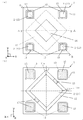
本実施形態における電子部品搭載用基板1は、主面(下面)に開口し、電子部品(第1電子部品21)を搭載する第1凹部12および他の主面(上面)に開口し、他の電子部品(第2電子部品22)を搭載する第2凹部13を有する絶縁基板11を有している。第1凹部12の底面が他の主面側に設けられており、第2凹部13の底面が主面側に設けられている。電子部品搭載用基板1は、絶縁基板11の主面および内部に設けられた配線導体15を有している。図1〜図3において、電子部品搭載用基板1および電子装置は仮想のxyz空間におけるxy平面に実装されている。図1〜図3において、上方向とは、仮想のz軸の正方向のことをいう。なお、以下の説明における上下の区別は便宜的なものであり、実際に電子部品搭載用基板1等が使用される際の上下を限定するものではない。
The electronic
絶縁基板11は、一方主面(図1〜図3では下面)および他方主面(図1〜図3では上面)と、側面とを有している。絶縁基板11は、複数の絶縁層からなり、一方主面に開口し、電子部品(第1電子部品21)を搭載する第1凹部12と、他方主面に開口し、他の電子部品
(第2電子部品22)を搭載する第2凹部13とを有しており、平面視すなわち主面に垂直な方向から見ると矩形の板状の形状を有している。絶縁基板11は電子部品2を支持するための支持体として機能し、第1凹部12の底面の搭載領域上および第2凹部13の底面の搭載領域上に、電子部品2がはんだバンプ、金バンプまたは導電性樹脂(異方性導電樹脂等)等の接続部材3を介して接着されて固定される。
The
絶縁基板11は、例えば、酸化アルミニウム質焼結体(アルミナセラミックス),窒化アルミニウム質焼結体,窒化珪素質焼結体、ムライト質焼結体またはガラスセラミックス焼結体等のセラミックスを用いることができる。絶縁基板11は、例えば酸化アルミニウム質焼結体である場合であれば、酸化アルミニウム(Al2O3),酸化珪素(SiO2),酸化マグネシウム(MgO),酸化カルシウム(CaO)等の原料粉末に適当な有機バインダーおよび溶剤等を添加混合して泥漿物を作製する。この泥漿物を、従来周知のドクターブレード法またはカレンダーロール法等を採用してシート状に成形することによってセラミックグリーンシートを作製する。次に、このセラミックグリーンシートに適当な打ち抜き加工を施すとともに、セラミックグリーンシートを複数枚積層して生成形体を形成し、この生成形体を高温(約1600℃)で焼成することによって絶縁基板11が製作される。
For the
第1凹部12は、絶縁基板11の一方主面に設けられている。第1凹部12は、底面に第1電子部品21を搭載するためのものである。第1凹部12の底面には、第1電子部品21と電気的に接続するための配線導体15が導出している。第2凹部13は、絶縁基板11の他方主面に設けられている。第2凹部13は、底面に第2電子部品22を搭載するためのものである。第2凹部13の底面には、第2電子部品22と電気的に接続するための配線導体15が導出している。第1凹部12の底面は、縦断面視において、第2凹部13の底面よりも、絶縁基板11の他方主面側に設けられている。第1凹部12と第2凹部13とは、平面透視において、互いに重ならないように配置されている。第2凹部13の底面は、縦断面視において、第1凹部12の底面よりも、絶縁基板11の一方主面側に設けられている。第2凹部13は、図1に示す例では、絶縁基板11の他方主面に、4つの第2凹部13が設けられており、4つの第2凹部13は、平面透視にて、第1凹部12を取り囲むように配置されている。第2凹部13は、平面透視において、第1凹部12よりも小さく形成されており、第2凹部13には、第1電子部品21よりも小型の第2電子部品22が搭載される。第1凹部12および第2凹部13は、図1〜図3に示す例では、平面視にて、角部が円弧状の矩形状としているが、平面視にて、多角形状、円形状、その他の形状であっても構わない。なお、絶縁基板11が、平面視にて矩形状としていると、小型の電子部品搭載用基板1を形成しやすい。
The
第1凹部12および第2凹部13は、例えば、絶縁基板11用のセラミックグリーンシートのいくつかにレーザー加工や金型による打ち抜き加工等によって、第1凹部12または第2凹部13となる貫通孔をそれぞれのセラミックグリーンシートに形成し、このセラミックグリーンシートを、貫通孔を形成していない他のセラミックグリーンシートに積層することで形成できる。
For example, the
配線導体15は、絶縁基板11の主面および内部に設けられている。配線導体15は、外部電極12とともに、電子部品搭載用基板1に搭載された電子部品2とモジュール用基板5とを電気的に接続するためのものである。配線導体15は、絶縁基板11の表面または内部に設けられた配線導体15と、絶縁基板11を構成する絶縁層を貫通して上下に位置する配線導体15同士を電気的に接続する貫通導体とを含んでいる。
The
配線導体15は、例えばタングステン(W),モリブデン(Mo),マンガン(Mn),銀(Ag)または銅(Cu)等を主成分とする金属粉末メタライズである。例えば、絶縁基板11が酸化アルミニウム質焼結体から成る場合であれば、W,MoまたはMn等の高融点金属粉末に適当な有機バインダーおよび溶媒等を添加混合して得たメタライズペースト
を、絶縁基板11用のセラミックグリーンシートに予めスクリーン印刷法によって所定のパターンに印刷塗布して、絶縁基板11用のセラミックグリーンシートと同時に焼成することによって、絶縁基板11の所定位置に被着形成される。配線導体15は、例えば、絶縁基板11用のセラミックグリーンシートに配線導体15用のメタライズペーストをスクリーン印刷法等の印刷手段によって印刷塗布し、絶縁基板11用のセラミックグリーンシートとともに焼成することによって形成される。また、配線導体15が貫通導体である場合は、例えば、絶縁基板11用のセラミックグリーンシートに金型またはパンチングによる打ち抜き加工またはレーザー加工等の加工方法によって貫通導体用の貫通孔を形成し、この貫通孔に貫通導体用のメタライズペーストを上記印刷手段によって充填しておき、絶縁基板11用のセラミックグリーンシートとともに焼成することによって形成される。メタライズペーストは、上述の金属粉末に適当な溶剤およびバインダーを加えて混練することによって、適度な粘度に調整して作製される。なお、絶縁基板11との接合強度を高めるために、ガラス粉末、セラミック粉末を含んでいても構わない。
The
配線導体15の絶縁基板11から露出する表面には、電気めっき法または無電解めっき法によって金属めっき層が被着される。金属めっき層は、ニッケル,銅,金または銀等の耐食性および接続部材3との接続性に優れる金属から成るものであり、例えば厚さ0.5〜5μ
m程度のニッケルめっき層と0.1〜3μm程度の金めっき層とが、あるいは厚さ1〜10μ
m程度のニッケルめっき層と0.1〜1μm程度の銀めっき層とが、順次被着される。これ
によって、配線導体15が腐食することを効果的に抑制できるとともに、配線導体15と電子部品2との固着および配線導体15とボンディングワイヤ等の接続部材3との接合、ならびに配線導体15とモジュール用基板5に形成された接続用の接続パッド51との接合を強固にできる。
A metal plating layer is applied to the surface of the
m nickel plating layer and 0.1-3 μm gold plating layer, or thickness 1-10 μm
A nickel plating layer of about m and a silver plating layer of about 0.1 to 1 μm are sequentially deposited. As a result, corrosion of the
また、金属めっき層は、ニッケルめっき層/金めっき層に限られるものではなく、ニッケルめっき層/金めっき層/銀めっき層、あるいはニッケルめっき層/パラジウムめっき層/金めっき層等を含むその他の金属めっき層であっても構わない。 In addition, the metal plating layer is not limited to the nickel plating layer / gold plating layer, but may include nickel plating layer / gold plating layer / silver plating layer or other nickel plating layer / palladium plating layer / gold plating layer. It may be a metal plating layer.
また、電子部品2が搭載される配線導体15上では、例えば上述のニッケルめっき層と金めっき層の下地層に、例えば、厚さ10〜80μm程度の銅めっき層を金属めっき層として被着させておくことにより、電子部品2の熱を銅めっき層を介して電子部品搭載用基板1側に良好に放熱させやすくしてもよい。
Further, on the
電子部品搭載用基板1の第1凹部12の底面に第1電子部品21を搭載し、電子部品搭載用基板1の第2凹部13の底面に第2電子部品22を搭載することによって、電子装置を作製できる。電子部品搭載用基板1に搭載される第1電子部品21は、受光素子、撮像素子、発光素子、ICチップまたはLSIチップ等の半導体素子等であり、第2電子部品22は、発光素子、抵抗素子、容量素子、ツェナーダイオード等である。例えば、第1電子部品21として、受光素子が用いられる場合、第2電子部品22として、発光素子が用いられる。第1電子部品21として、例えば、光学素子が用いられる場合、図1および図2に示す例のように、第1凹部12の底面に、絶縁基板11の他方主面と第1凹部12の底面とを貫通する開口部14が設けられる。光学素子は、受光面を開口部14側に向けて第1凹部12に搭載されており、第1凹部12に搭載された光学素子に外部の光が開口部14を介して入射して受光されるようにしている。開口部14は、凹部と同様に、絶縁基板11用のセラミックグリーンシートのいくつかにレーザー加工や金型による打ち抜き加工等によって、開口部14となる貫通孔をセラミックグリーンシートに形成しておくことにより形成できる。例えば電子部品2がフリップチップ型の半導体素子である場合には、半導体素子は、はんだバンプ、金バンプまたは導電性樹脂(異方性導電樹脂等)等の接続部材3を介して、半導体素子の電極と配線導体15とが電気的および機械的に接続されることによって電子部品搭載用基板1に搭載される。また、例えば、電子部品2がワイヤボンディング型の半導体素子である場合には、半
導体素子は、低融点ろう材または導電性樹脂等の接合部材によって、配線導体15上に固定された後、ボンディングワイヤ等の接続部材3を介して半導体素子の電極と配線導体15とが電気的に接続されることによって電子部品搭載用基板1に搭載される。これにより、電子部品2は外部電極12に電気的に接続される。また、電子部品2は必要に応じて、樹脂またはガラス等からなる封止材を用いて、樹脂、ガラス、セラミックスまたは金属等からなる蓋体等により封止される。
By mounting the first
本実施形態の電子装置の配線導体15が、図3に示すように、図3に示すように、モジュール用基板5の接続パッド51にはんだ6を介して接続されて、電子モジュールとなる。
As shown in FIG. 3, the
また、配線導体15が、図1に示す例のように、平面透視において、第2凹部13よりも大きく、第2凹部13と重なるように絶縁基板11の一方主面に配置されていると、電子装置を作動させた際に、第2凹部13に搭載された第2電子部品22の熱を配線導体15を介して、モジュール用基板5側に伝わりやすくすることができ、第2電子部品22の絶縁基板11における第1凹部12側への伝熱、すなわち、第1電子部品21側への伝熱を抑制することができる。
In addition, when the
また、電子装置を作動させた際に発生する第2電子部品22の熱を、モジュール用基板5へ伝わりやすいものとしており、絶縁基板11の下面と第2凹部13の底面との間における絶縁基板11の厚みが小さいため、モジュール用基板5への伝熱をより良好なものとすることができ、熱による絶縁基板11の歪みにより第2凹部13における底面と側壁との間に亀裂が生じることを抑制することができるので、薄型の電子部品搭載用基板1として有効である。
Further, the heat of the second
また、第2凹部13の底面と絶縁基板11の一方主面に設けられた配線導体15との間隔が、第1凹部12の底面と第2凹部13の底面との間隔よりも小さいと、第2凹部13に搭載された第2電子部品22の熱を配線導体15を介して、モジュール用基板5に伝わりやすくし、第1凹部12側への伝熱を抑制することができる。第2凹部13の底面と絶縁基板11の一方主面に設けられた配線導体15との間隔は、第1凹部12の底面と第2凹部13の底面との間隔の1/2以下であることがより好ましい。
Further, if the distance between the bottom surface of the
本実施形態の電子部品搭載用基板1は、主面に開口し、電子部品(第1電子部品21)を搭載する第1凹部12および他の主面に開口し、他の電子部品(第2電子部品22)を搭載する第2凹部13を有する絶縁基板11を有しており、第1凹部12の底面が他の主面側に設けられており、第2凹部13の底面が主面側に設けられている。上記構成により、絶縁基板11における、電子部品(第1電子部品21)を搭載する第1凹部12の底面と、他の電子部品(第2電子部品22)を搭載する第2凹部13の底面との間の伝熱経路が実質的に長くなり、電子装置を作動させた際に、他の電子部品の熱が絶縁基板11における電子部品の周囲に伝わるのを抑制し、電子部品搭載用基板1と電子部品との接合信頼性が低下するのを抑制することができる。また、電子装置を作動させた際に、絶縁基板11における電子部品の周囲が歪みやすくなり、電子部品が傾くのを抑制し、例えば電子部品が受光素子の場合に良好に受光することができる。
The electronic
また、第1電子部品21として、受光素子等の光学素子が用いられる場合、第2電子部品22から第1電子部品21周囲の絶縁基板11への伝熱が抑制され、受光素子等の光学素子にて外部の光を良好に受光することができる。
When an optical element such as a light receiving element is used as the first
本実施形態の電子装置は、上記構成の電子部品搭載用基板1と、第1凹部12に搭載された電子部品(第1電子部品21)と、第2凹部13に搭載された他の電子部品(第2電子部品22)とを有していることによって、長期信頼性に優れた電子装置とすることができる。
The electronic device according to the present embodiment includes the electronic
本実施形態の電子モジュールは、接続パッド51を有するモジュール用基板5と、接続パッド51にはんだ6を介して接続された上記構成の電子装置とを有していることによって、長期信頼性に優れたものとすることができる。
The electronic module of the present embodiment has excellent long-term reliability by including the module substrate 5 having the
本実施形態における電子部品搭載用基板1は、小型で高出力の電子装置において好適に使用することができ、電子部品搭載用基板1における接続信頼性を高めることができる。例えば、第1電子部品21として、受光素子が用いられ、第2電子部品22として、発光素子が用いられる小型の電子部品搭載用基板1として好適に用いることができる。
The electronic
(第2の実施形態)
次に、本発明の第2の実施形態による電子装置について、図4および図5を参照しつつ説明する。
(Second Embodiment)
Next, an electronic device according to a second embodiment of the present invention will be described with reference to FIGS.
本発明の第2の実施形態における電子装置において、第1凹部12が絶縁基板11の中央部に設けられ、第2凹部13が絶縁基板11の角部に設けられている。
In the electronic device according to the second embodiment of the present invention, the
本発明の第2の実施形態における電子部品搭載用基板1によれば、第1の実施形態の配線基板1と同様に、絶縁基板11における、電子部品(第1電子部品21)を搭載する第1凹部12の底面と、他の電子部品(第2電子部品22)を搭載する第2凹部22の底面との間の伝熱経路が実質的に長くなり、電子装置を作動させた際に、他の電子部品の熱が絶縁基板11における電子部品の周囲に伝わるのを抑制し、電子部品搭載用基板1と電子部品との接合信頼性が低下するのを抑制することができる。また、電子装置を作動させた際に、絶縁基板11における電子部品の周囲が歪みやすくなり、電子部品が傾くのを抑制し、例えば電子部品が受光素子の場合に良好に受光することができる。
According to the electronic
第2の実施形態における電子部品搭載用基板1によれば、絶縁基板11は平面視で矩形状であり、平面透視において、第1凹部12は絶縁基板11の中央部に設けられ、第2凹部13は絶縁基板11の角部に設けられていることから、第1の実施形態の電子部品搭載用基板1と比較して、絶縁基板11の角部を広い領域とすることができ、第2凹部13を絶縁基板11の角部の広い領域に設けることができるので、第1凹部12と第2凹部13との間隔を広くし、第2電子部品22の熱が第1電子部品21側に伝熱するのを抑制することができるとともに、第1凹部12と第2凹部13との間の絶縁基板11の厚みが大きくなり、絶縁基板11に生じる歪みを抑制することができる。
According to the electronic
第1凹部12は平面透視で矩形状であり、各隅部が絶縁基板11の角部に挟まれる位置に設けられていることから、絶縁基板11の角部の領域を良好に広くすることができ、第2凹部13を絶縁基板11の角部の広い領域に設けることができるので、第1凹部12と第2凹部13との間隔を広くし、電子装置を作動させた際に、第2電子部品22の熱が絶縁基板11における第1電子部品21側に伝わるのを抑制し、電子部品搭載用基板1と第1電子部品21との接合信頼性が低下するのを抑制することができる。また絶縁基板11における第1凹部12と第2凹部13との間の厚みが厚いものとなり、絶縁基板11に生じる歪みを抑制し、第1電子部品21が傾くのを抑制することができる。
The
第1凹部12は平面透視で矩形状であり、第1凹部12における対角に位置する一組の隅部が、絶縁基板11の対向する一組の辺に対し垂直に交わる仮想直線11a上に設けられていることから、絶縁基板11の角部の領域を偏りなく広くすることができ、第2凹部13を絶縁基板11の角部の広い領域に設けることができるので、第1凹部12と第2凹部13との間隔を広くし、電子装置を作動させた際に、第2電子部品22の熱が絶縁基板11における第1電子部品21側に伝わるのを抑制することができ、電子部品搭載用基板1と電子部品との接合信頼
性が低下するのを抑制することができる。また、絶縁基板11における第1凹部12と第2凹部13との間の厚みが厚いものとなり、絶縁基板11に生じる歪みを抑制し、第1電子部品21が傾くのを抑制することができる。
The
第2の実施形態の電子部品搭載用基板1は、第1の実施形態と同様に、小型で高出力の電子装置において好適に使用することができ、電子部品搭載用基板1における接続信頼性を高めることができる。例えば、第1電子部品21として、受光素子が用いられ、第2電子部品22として、発光素子が用いられる小型の電子部品搭載用基板1として好適に用いることができる。
Similarly to the first embodiment, the electronic
第2の実施形態の電子部品搭載用基板1は、上述の第1の実施形態の電子部品搭載用基板1と同様の製造方法を用いて製作することができる。
The electronic
(第3の実施形態)
次に、本発明の第3の実施形態による電子装置について、図6および図7を参照しつつ説明する。
(Third embodiment)
Next, an electronic device according to a third embodiment of the present invention will be described with reference to FIGS.
本発明の第3の実施形態における電子装置において、第1凹部12が絶縁基板11の中央部に設けられ、第2凹部13が絶縁基板11の角部に設けられており、第2凹部13における第1凹部12側の側面と、第1凹部12における第2凹部13側の側面とが平行である。
In the electronic device according to the third embodiment of the present invention, the
本発明の第3の実施形態における電子部品搭載用基板1によれば、第1の実施形態における電子部品搭載用基板1と同様に、絶縁基板11における、電子部品を搭載する第1凹部の底面と、他の電子部品を搭載する第2凹部の底面との間の伝熱経路が実質的に長くなり、電子装置を作動させた際に、他の電子部品の熱が絶縁基板11における電子部品の周囲に伝わるのを抑制し、電子部品搭載用基板1と電子部品との接合信頼性が低下するのを抑制することができる。また、電子装置を作動させた際に、絶縁基板11における電子部品の周囲が歪みやすくなり、電子部品が傾くのを抑制し、例えば電子部品が受光素子の場合に良好に受光することができる。
According to the electronic
また、第2凹部13における第1凹部12側の側面と、第1凹部12における第2凹部13側の側面とが平行であることにより、第1凹部12の隅部と第2凹部13の隅部とが対向していないので、第1凹部12と第2凹部13との間における絶縁基板11の厚みが局所的に小さくなることがなくなり、第1電子部品21または第2電子部品22の作動による生じる熱により、絶縁基板11における第1凹部12と第2凹部13との間に亀裂等が生じることを抑制することができる。
Further, since the side surface of the
第3の実施形態の電子部品搭載用基板1は、第1の実施形態と同様に、小型で高出力の電子装置において好適に使用することができ、電子部品搭載用基板1における接続信頼性を高めることができる。例えば、第1電子部品21として、受光素子が用いられ、第2電子部品22として、発光素子が用いられる小型の電子部品搭載用基板1として好適に用いることができる。
Similarly to the first embodiment, the electronic
第3の実施形態の電子部品搭載用基板1は、上述の第1の実施形態の電子部品搭載用基板1と同様の製造方法を用いて製作することができる。
The electronic
(第4の実施形態)
次に、本発明の第4の実施形態による電子装置について、図8および図9を参照しつつ説明する。
(Fourth embodiment)
Next, an electronic device according to a fourth embodiment of the present invention will be described with reference to FIGS.
本発明の第4の実施形態における電子装置において、上記した第1の実施形態の電子装置と異なる点は、第2凹部13の底面に、絶縁基板11の一方主面(下面)と第2凹部13の底面とを貫通する開口部14が設けられる点、絶縁基板11の他方主面(上面)における第1凹部12の底面と重なる領域に、配線導体15が設けられている点である。
The electronic device according to the fourth embodiment of the present invention differs from the electronic device according to the first embodiment described above in that one main surface (lower surface) of the insulating
本発明の第4の実施形態における電子部品搭載用基板1によれば、第1の実施形態における電子部品搭載用基板1と同様に、絶縁基板11における、電子部品を搭載する第1凹部の底面と、他の電子部品を搭載する第2凹部の底面との間の伝熱経路が実質的に長くなり、電子装置を作動させた際に、電子部品の熱が絶縁基板11における他の電子部品の周囲に伝わるのを抑制し、電子部品搭載用基板1と他の電子部品との接合信頼性が低下するのを抑制することができる。また、電子装置を作動させた際に、絶縁基板11における電子部品の周囲が歪みやすくなり、電子部品が傾くのを抑制し、例えば電子部品が受光素子の場合に良好に受光することができる。
According to the electronic
また、配線導体15が、平面透視において、第1凹部12と重なり、第1凹部12を囲むように絶縁基板11の他方主面に配置されていると、電子装置を作動させた際に、第1凹部12に搭載された第1電子部品21の熱を配線導体15を介して、モジュール用基板5側に伝わりやすくすることができ、第1電子部品21の絶縁基板11における第2凹部13側への伝熱、すなわち、第2電子部品22側への伝熱を抑制することができる。
In addition, when the
第4の実施形態の電子部品搭載用基板1は、第1の実施形態と同様に、小型で高出力の電子装置において好適に使用することができ、電子部品搭載用基板1における接続信頼性を高めることができる。例えば、第1電子部品21として、受光素子が用いられ、第2電子部品22として、発光素子が用いられる小型の電子部品搭載用基板1として好適に用いることができる。
Similar to the first embodiment, the electronic
第4の実施形態の電子部品搭載用基板1は、上述の第1の実施形態の電子部品搭載用基板1と同様の製造方法を用いて製作することができる。
The electronic
本発明は、上述の実施の形態の例に限定されるものではなく、種々の変更は可能である。例えば、配線導体15は、絶縁基板11の側面と一方主面との間に切欠きが設けられており、切欠きの内面に配線導体15が延出された、いわゆるキャスタレーション導体を有していてもよい。
The present invention is not limited to the above-described embodiments, and various modifications can be made. For example, the
また、第1〜第4の実施形態における電子部品搭載用基板1は、第1凹部12および第2凹部13は、縦断面視において、側壁が垂直形状に形成しているが、第1凹部12または第2凹部13は、縦断面視において、側壁が、底面側よりも開口側が広くなるような階段状の凹部であっても構わない。また、第1凹部12または第2凹部13は、平面透視において、凹部の開口側の大きさが、凹部の底面側の大きさよりも小さい凹部であっても構わない。
Further, in the electronic
また、電子部品搭載用基板1は、多数個取り電子部品搭載用基板の形態で製作されていてもよい。
The electronic
1・・・・電子部品搭載用基板
11・・・・絶縁基板
11a・・・仮想直線
12・・・・第1凹部
13・・・・第2凹部
14・・・・開口部
15・・・・配線導体
2・・・・電子部品
21・・・・第1電子部品
22・・・・第2電子部品
3・・・・接続部材
5・・・・モジュール用基板
51・・・・接続パッド
6・・・・はんだ
1 .... Electronic component mounting board
11 ... Insulating substrate
11a ... Virtual straight line
12 ··· First recess
13 ... Second recess
14 ... Opening
15 ...
21 ... 1st electronic component
22 ... Second
51 ...
Claims (7)
前記第1凹部の底面が前記他の主面側に設けられ、
前記第2凹部の底面が前記主面側に設けられており、
平面透視において、前記第2凹部よりも大きく、前記第2凹部が収まるように前記主面に配置された配線導体を有していることを特徴とする電子部品搭載用基板。 Open to the major surface, a first recess for mounting the electronic components, and opened to the other main surface, it has a dielectric substrate having a second recess for mounting the other electronic components,
The bottom surface of the first recess is found provided on the other main surface,
A bottom surface of the second recess is provided on the main surface side ;
An electronic component mounting board comprising: a wiring conductor disposed on the main surface so as to be larger than the second recess and accommodated in the second recess, as seen in a plan view .
平面透視において、前記第1凹部は前記絶縁基板の中央部に設けられ、前記第2凹部は前記絶縁基板の角部に設けられていることを特徴とする請求項1に記載の電子部品搭載用基板。 The insulating substrate is rectangular in plan view,
2. The electronic component mounting device according to claim 1, wherein the first concave portion is provided in a central portion of the insulating substrate and the second concave portion is provided in a corner portion of the insulating substrate when seen in a plan view. substrate.
前記第2凹部における前記第1凹部側の側面と、前記第1凹部における前記第2凹部側の側面とが平行であることを特徴とする請求項3または請求項4に記載の電子部品搭載用基板。 The second recess is rectangular in plan view,
5. The electronic component mounting device according to claim 3, wherein a side surface of the second recess portion on the side of the first recess portion and a side surface of the first recess portion on the side of the second recess portion are parallel to each other. substrate.
前記第1凹部に搭載された電子部品と、
前記第2凹部に搭載された他の電子部品とを有することを特徴とする電子装置。 An electronic component mounting substrate according to any one of claims 1 to 5,
An electronic component mounted in the first recess;
An electronic device comprising: another electronic component mounted in the second recess.
前記接続パッドにはんだを介して接続された請求項6に記載の電子装置とを有することを特徴とする電子モジュール。 A module substrate having connection pads;
An electronic module comprising: the electronic device according to claim 6 connected to the connection pad via solder.
Priority Applications (1)
| Application Number | Priority Date | Filing Date | Title |
|---|---|---|---|
| JP2015224032A JP6595308B2 (en) | 2015-11-16 | 2015-11-16 | Electronic component mounting substrate, electronic device and electronic module |
Applications Claiming Priority (1)
| Application Number | Priority Date | Filing Date | Title |
|---|---|---|---|
| JP2015224032A JP6595308B2 (en) | 2015-11-16 | 2015-11-16 | Electronic component mounting substrate, electronic device and electronic module |
Publications (2)
| Publication Number | Publication Date |
|---|---|
| JP2017092380A JP2017092380A (en) | 2017-05-25 |
| JP6595308B2 true JP6595308B2 (en) | 2019-10-23 |
Family
ID=58771132
Family Applications (1)
| Application Number | Title | Priority Date | Filing Date |
|---|---|---|---|
| JP2015224032A Active JP6595308B2 (en) | 2015-11-16 | 2015-11-16 | Electronic component mounting substrate, electronic device and electronic module |
Country Status (1)
| Country | Link |
|---|---|
| JP (1) | JP6595308B2 (en) |
Family Cites Families (10)
| Publication number | Priority date | Publication date | Assignee | Title |
|---|---|---|---|---|
| JPS5746624Y2 (en) * | 1975-03-27 | 1982-10-14 | ||
| JPH04359462A (en) * | 1991-06-05 | 1992-12-11 | Toyota Motor Corp | Hybrid integrated circuit device |
| JPH0613535A (en) * | 1992-06-26 | 1994-01-21 | Ibiden Co Ltd | Electronic part mounting apparatus |
| JPH0722728A (en) * | 1993-07-06 | 1995-01-24 | Ibiden Co Ltd | Substrate for mounting electronic component |
| JP2000124400A (en) * | 1998-10-12 | 2000-04-28 | Hitachi Maxell Ltd | Semiconductor device |
| JP5024317B2 (en) * | 2002-03-25 | 2012-09-12 | セイコーエプソン株式会社 | Electronic component and method for manufacturing electronic component |
| JP4046088B2 (en) * | 2004-02-02 | 2008-02-13 | 松下電器産業株式会社 | Three-dimensional electronic circuit device and its relay substrate and relay frame |
| US7613010B2 (en) * | 2004-02-02 | 2009-11-03 | Panasonic Corporation | Stereoscopic electronic circuit device, and relay board and relay frame used therein |
| JP2008135788A (en) * | 2008-02-25 | 2008-06-12 | Mitsubishi Electric Corp | Semiconductor device |
| JP6034158B2 (en) * | 2012-11-29 | 2016-11-30 | 京セラ株式会社 | Wiring board and mounting structure using the same |
-
2015
- 2015-11-16 JP JP2015224032A patent/JP6595308B2/en active Active
Also Published As
| Publication number | Publication date |
|---|---|
| JP2017092380A (en) | 2017-05-25 |
Similar Documents
| Publication | Publication Date | Title |
|---|---|---|
| US11145587B2 (en) | Electronic component mounting substrate, electronic device, and electronic module | |
| JP6791719B2 (en) | Substrate for mounting electronic components, electronic devices and electronic modules | |
| JP6767204B2 (en) | Boards for mounting electronic components, electronic devices and electronic modules | |
| JP6698826B2 (en) | Substrate for mounting electronic parts, electronic device and electronic module | |
| JP6626735B2 (en) | Electronic component mounting board, electronic device and electronic module | |
| CN107615893B (en) | Circuit board, electronic device and electronic module | |
| CN111033771B (en) | Substrate for mounting electronic component, electronic device, and electronic module | |
| JP6780996B2 (en) | Wiring boards, electronics and electronic modules | |
| JP2023071984A (en) | Wiring boards, electronic devices and electronic modules | |
| JP6698301B2 (en) | Wiring board, electronic device and electronic module | |
| CN113228258B (en) | Wiring substrate, electronic device, and electronic module | |
| JP6595308B2 (en) | Electronic component mounting substrate, electronic device and electronic module | |
| CN107431047B (en) | Wiring board, electronic device, and electronic module | |
| JP6737646B2 (en) | Wiring board, electronic device and electronic module | |
| WO2018155559A1 (en) | Wiring substrate, electronic device, and electronic module | |
| JP6633381B2 (en) | Electronic component mounting board, electronic device and electronic module | |
| JPWO2018155434A1 (en) | Wiring board, electronic device and electronic module | |
| JP6687435B2 (en) | Wiring board, electronic device and electronic module |
Legal Events
| Date | Code | Title | Description |
|---|---|---|---|
| A621 | Written request for application examination |
Free format text: JAPANESE INTERMEDIATE CODE: A621 Effective date: 20180827 |
|
| A977 | Report on retrieval |
Free format text: JAPANESE INTERMEDIATE CODE: A971007 Effective date: 20190422 |
|
| A131 | Notification of reasons for refusal |
Free format text: JAPANESE INTERMEDIATE CODE: A131 Effective date: 20190507 |
|
| A521 | Written amendment |
Free format text: JAPANESE INTERMEDIATE CODE: A523 Effective date: 20190702 |
|
| TRDD | Decision of grant or rejection written | ||
| A01 | Written decision to grant a patent or to grant a registration (utility model) |
Free format text: JAPANESE INTERMEDIATE CODE: A01 Effective date: 20190827 |
|
| A61 | First payment of annual fees (during grant procedure) |
Free format text: JAPANESE INTERMEDIATE CODE: A61 Effective date: 20190926 |
|
| R150 | Certificate of patent or registration of utility model |
Ref document number: 6595308 Country of ref document: JP Free format text: JAPANESE INTERMEDIATE CODE: R150 |