JP6222771B2 - 炭化珪素半導体装置の製造方法 - Google Patents
炭化珪素半導体装置の製造方法 Download PDFInfo
- Publication number
- JP6222771B2 JP6222771B2 JP2013242367A JP2013242367A JP6222771B2 JP 6222771 B2 JP6222771 B2 JP 6222771B2 JP 2013242367 A JP2013242367 A JP 2013242367A JP 2013242367 A JP2013242367 A JP 2013242367A JP 6222771 B2 JP6222771 B2 JP 6222771B2
- Authority
- JP
- Japan
- Prior art keywords
- semiconductor region
- silicon carbide
- semiconductor device
- layer
- concentration
- Prior art date
- Legal status (The legal status is an assumption and is not a legal conclusion. Google has not performed a legal analysis and makes no representation as to the accuracy of the status listed.)
- Active
Links
- 239000004065 semiconductor Substances 0.000 title claims description 183
- 229910010271 silicon carbide Inorganic materials 0.000 title claims description 135
- HBMJWWWQQXIZIP-UHFFFAOYSA-N silicon carbide Chemical compound [Si+]#[C-] HBMJWWWQQXIZIP-UHFFFAOYSA-N 0.000 title claims description 133
- 238000004519 manufacturing process Methods 0.000 title claims description 39
- 238000000034 method Methods 0.000 title claims description 23
- 239000000758 substrate Substances 0.000 claims description 96
- 239000010410 layer Substances 0.000 claims description 75
- 239000012535 impurity Substances 0.000 claims description 45
- PXHVJJICTQNCMI-UHFFFAOYSA-N Nickel Chemical compound [Ni] PXHVJJICTQNCMI-UHFFFAOYSA-N 0.000 claims description 26
- OKTJSMMVPCPJKN-UHFFFAOYSA-N Carbon Chemical compound [C] OKTJSMMVPCPJKN-UHFFFAOYSA-N 0.000 claims description 23
- 229910052799 carbon Inorganic materials 0.000 claims description 23
- 238000010438 heat treatment Methods 0.000 claims description 19
- XUIMIQQOPSSXEZ-UHFFFAOYSA-N Silicon Chemical compound [Si] XUIMIQQOPSSXEZ-UHFFFAOYSA-N 0.000 claims description 17
- 229910052751 metal Inorganic materials 0.000 claims description 17
- 239000002184 metal Substances 0.000 claims description 17
- 229910052710 silicon Inorganic materials 0.000 claims description 17
- 239000010703 silicon Substances 0.000 claims description 17
- 229910021334 nickel silicide Inorganic materials 0.000 claims description 16
- RUFLMLWJRZAWLJ-UHFFFAOYSA-N nickel silicide Chemical compound [Ni]=[Si]=[Ni] RUFLMLWJRZAWLJ-UHFFFAOYSA-N 0.000 claims description 16
- IJGRMHOSHXDMSA-UHFFFAOYSA-N Atomic nitrogen Chemical compound N#N IJGRMHOSHXDMSA-UHFFFAOYSA-N 0.000 claims description 12
- 229910052759 nickel Inorganic materials 0.000 claims description 12
- 239000010936 titanium Substances 0.000 claims description 12
- RTAQQCXQSZGOHL-UHFFFAOYSA-N Titanium Chemical compound [Ti] RTAQQCXQSZGOHL-UHFFFAOYSA-N 0.000 claims description 10
- 230000001133 acceleration Effects 0.000 claims description 10
- 229910052719 titanium Inorganic materials 0.000 claims description 10
- 239000002344 surface layer Substances 0.000 claims description 8
- OAICVXFJPJFONN-UHFFFAOYSA-N Phosphorus Chemical compound [P] OAICVXFJPJFONN-UHFFFAOYSA-N 0.000 claims description 7
- 229910052782 aluminium Inorganic materials 0.000 claims description 7
- XAGFODPZIPBFFR-UHFFFAOYSA-N aluminium Chemical compound [Al] XAGFODPZIPBFFR-UHFFFAOYSA-N 0.000 claims description 7
- 229910052698 phosphorus Inorganic materials 0.000 claims description 7
- 239000011574 phosphorus Substances 0.000 claims description 7
- KRHYYFGTRYWZRS-UHFFFAOYSA-N Fluorane Chemical compound F KRHYYFGTRYWZRS-UHFFFAOYSA-N 0.000 claims description 6
- 238000003763 carbonization Methods 0.000 claims description 6
- 229910052757 nitrogen Inorganic materials 0.000 claims description 6
- 230000001681 protective effect Effects 0.000 claims description 6
- ZOXJGFHDIHLPTG-UHFFFAOYSA-N Boron Chemical compound [B] ZOXJGFHDIHLPTG-UHFFFAOYSA-N 0.000 claims description 4
- 230000004913 activation Effects 0.000 claims description 4
- 229910052796 boron Inorganic materials 0.000 claims description 4
- 239000011777 magnesium Substances 0.000 claims description 4
- GYHNNYVSQQEPJS-UHFFFAOYSA-N Gallium Chemical compound [Ga] GYHNNYVSQQEPJS-UHFFFAOYSA-N 0.000 claims description 3
- FYYHWMGAXLPEAU-UHFFFAOYSA-N Magnesium Chemical compound [Mg] FYYHWMGAXLPEAU-UHFFFAOYSA-N 0.000 claims description 3
- 229910052785 arsenic Inorganic materials 0.000 claims description 3
- RQNWIZPPADIBDY-UHFFFAOYSA-N arsenic atom Chemical compound [As] RQNWIZPPADIBDY-UHFFFAOYSA-N 0.000 claims description 3
- 238000005530 etching Methods 0.000 claims description 3
- 229910052733 gallium Inorganic materials 0.000 claims description 3
- 229910052749 magnesium Inorganic materials 0.000 claims description 3
- 230000003647 oxidation Effects 0.000 claims description 3
- 238000007254 oxidation reaction Methods 0.000 claims description 3
- 238000005468 ion implantation Methods 0.000 description 21
- VZSRBBMJRBPUNF-UHFFFAOYSA-N 2-(2,3-dihydro-1H-inden-2-ylamino)-N-[3-oxo-3-(2,4,6,7-tetrahydrotriazolo[4,5-c]pyridin-5-yl)propyl]pyrimidine-5-carboxamide Chemical compound C1C(CC2=CC=CC=C12)NC1=NC=C(C=N1)C(=O)NCCC(N1CC2=C(CC1)NN=N2)=O VZSRBBMJRBPUNF-UHFFFAOYSA-N 0.000 description 8
- 238000000151 deposition Methods 0.000 description 8
- 230000008021 deposition Effects 0.000 description 7
- 239000011229 interlayer Substances 0.000 description 7
- 230000000052 comparative effect Effects 0.000 description 6
- 238000012360 testing method Methods 0.000 description 6
- 238000009792 diffusion process Methods 0.000 description 5
- 238000005240 physical vapour deposition Methods 0.000 description 5
- AFCARXCZXQIEQB-UHFFFAOYSA-N N-[3-oxo-3-(2,4,6,7-tetrahydrotriazolo[4,5-c]pyridin-5-yl)propyl]-2-[[3-(trifluoromethoxy)phenyl]methylamino]pyrimidine-5-carboxamide Chemical compound O=C(CCNC(=O)C=1C=NC(=NC=1)NCC1=CC(=CC=C1)OC(F)(F)F)N1CC2=C(CC1)NN=N2 AFCARXCZXQIEQB-UHFFFAOYSA-N 0.000 description 4
- 230000015556 catabolic process Effects 0.000 description 4
- 238000004544 sputter deposition Methods 0.000 description 4
- 238000004380 ashing Methods 0.000 description 3
- 125000004432 carbon atom Chemical group C* 0.000 description 3
- 238000007796 conventional method Methods 0.000 description 3
- 230000005684 electric field Effects 0.000 description 3
- 239000010931 gold Substances 0.000 description 3
- 238000001020 plasma etching Methods 0.000 description 3
- 238000012545 processing Methods 0.000 description 3
- 238000005245 sintering Methods 0.000 description 3
- XKRFYHLGVUSROY-UHFFFAOYSA-N Argon Chemical compound [Ar] XKRFYHLGVUSROY-UHFFFAOYSA-N 0.000 description 2
- 230000004888 barrier function Effects 0.000 description 2
- 238000005229 chemical vapour deposition Methods 0.000 description 2
- 238000001816 cooling Methods 0.000 description 2
- 239000013078 crystal Substances 0.000 description 2
- 230000000694 effects Effects 0.000 description 2
- 239000007789 gas Substances 0.000 description 2
- PCHJSUWPFVWCPO-UHFFFAOYSA-N gold Chemical compound [Au] PCHJSUWPFVWCPO-UHFFFAOYSA-N 0.000 description 2
- 229910052737 gold Inorganic materials 0.000 description 2
- 238000002513 implantation Methods 0.000 description 2
- 239000000463 material Substances 0.000 description 2
- 238000000206 photolithography Methods 0.000 description 2
- MYMOFIZGZYHOMD-UHFFFAOYSA-N Dioxygen Chemical compound O=O MYMOFIZGZYHOMD-UHFFFAOYSA-N 0.000 description 1
- 238000000137 annealing Methods 0.000 description 1
- 229910052786 argon Inorganic materials 0.000 description 1
- QVGXLLKOCUKJST-UHFFFAOYSA-N atomic oxygen Chemical compound [O] QVGXLLKOCUKJST-UHFFFAOYSA-N 0.000 description 1
- 239000000969 carrier Substances 0.000 description 1
- 238000006243 chemical reaction Methods 0.000 description 1
- 230000003247 decreasing effect Effects 0.000 description 1
- 238000010586 diagram Methods 0.000 description 1
- 229910001882 dioxygen Inorganic materials 0.000 description 1
- 239000002019 doping agent Substances 0.000 description 1
- 230000005669 field effect Effects 0.000 description 1
- 238000002347 injection Methods 0.000 description 1
- 239000007924 injection Substances 0.000 description 1
- 150000002500 ions Chemical class 0.000 description 1
- 239000001301 oxygen Substances 0.000 description 1
- 229910052760 oxygen Inorganic materials 0.000 description 1
- 230000000737 periodic effect Effects 0.000 description 1
- 230000000704 physical effect Effects 0.000 description 1
- 230000001698 pyrogenic effect Effects 0.000 description 1
- 238000011160 research Methods 0.000 description 1
- 229910021332 silicide Inorganic materials 0.000 description 1
- FVBUAEGBCNSCDD-UHFFFAOYSA-N silicide(4-) Chemical compound [Si-4] FVBUAEGBCNSCDD-UHFFFAOYSA-N 0.000 description 1
- MTPVUVINMAGMJL-UHFFFAOYSA-N trimethyl(1,1,2,2,2-pentafluoroethyl)silane Chemical compound C[Si](C)(C)C(F)(F)C(F)(F)F MTPVUVINMAGMJL-UHFFFAOYSA-N 0.000 description 1
Images


Classifications
-
- H—ELECTRICITY
- H10—SEMICONDUCTOR DEVICES; ELECTRIC SOLID-STATE DEVICES NOT OTHERWISE PROVIDED FOR
- H10D—INORGANIC ELECTRIC SEMICONDUCTOR DEVICES
- H10D8/00—Diodes
- H10D8/60—Schottky-barrier diodes
- H10D8/605—Schottky-barrier diodes of the trench conductor-insulator-semiconductor barrier type, e.g. trench MOS barrier Schottky rectifiers [TMBS]
-
- H—ELECTRICITY
- H01—ELECTRIC ELEMENTS
- H01L—SEMICONDUCTOR DEVICES NOT COVERED BY CLASS H10
- H01L21/00—Processes or apparatus adapted for the manufacture or treatment of semiconductor or solid state devices or of parts thereof
- H01L21/02—Manufacture or treatment of semiconductor devices or of parts thereof
- H01L21/04—Manufacture or treatment of semiconductor devices or of parts thereof the devices having potential barriers, e.g. a PN junction, depletion layer or carrier concentration layer
- H01L21/0445—Manufacture or treatment of semiconductor devices or of parts thereof the devices having potential barriers, e.g. a PN junction, depletion layer or carrier concentration layer the devices having semiconductor bodies comprising crystalline silicon carbide
- H01L21/0455—Making n or p doped regions or layers, e.g. using diffusion
- H01L21/046—Making n or p doped regions or layers, e.g. using diffusion using ion implantation
-
- H—ELECTRICITY
- H01—ELECTRIC ELEMENTS
- H01L—SEMICONDUCTOR DEVICES NOT COVERED BY CLASS H10
- H01L21/00—Processes or apparatus adapted for the manufacture or treatment of semiconductor or solid state devices or of parts thereof
- H01L21/02—Manufacture or treatment of semiconductor devices or of parts thereof
- H01L21/04—Manufacture or treatment of semiconductor devices or of parts thereof the devices having potential barriers, e.g. a PN junction, depletion layer or carrier concentration layer
- H01L21/0445—Manufacture or treatment of semiconductor devices or of parts thereof the devices having potential barriers, e.g. a PN junction, depletion layer or carrier concentration layer the devices having semiconductor bodies comprising crystalline silicon carbide
- H01L21/048—Making electrodes
- H01L21/0495—Schottky electrodes
-
- H—ELECTRICITY
- H10—SEMICONDUCTOR DEVICES; ELECTRIC SOLID-STATE DEVICES NOT OTHERWISE PROVIDED FOR
- H10D—INORGANIC ELECTRIC SEMICONDUCTOR DEVICES
- H10D62/00—Semiconductor bodies, or regions thereof, of devices having potential barriers
- H10D62/10—Shapes, relative sizes or dispositions of the regions of the semiconductor bodies; Shapes of the semiconductor bodies
- H10D62/102—Constructional design considerations for preventing surface leakage or controlling electric field concentration
- H10D62/103—Constructional design considerations for preventing surface leakage or controlling electric field concentration for increasing or controlling the breakdown voltage of reverse-biased devices
- H10D62/105—Constructional design considerations for preventing surface leakage or controlling electric field concentration for increasing or controlling the breakdown voltage of reverse-biased devices by having particular doping profiles, shapes or arrangements of PN junctions; by having supplementary regions, e.g. junction termination extension [JTE]
- H10D62/106—Constructional design considerations for preventing surface leakage or controlling electric field concentration for increasing or controlling the breakdown voltage of reverse-biased devices by having particular doping profiles, shapes or arrangements of PN junctions; by having supplementary regions, e.g. junction termination extension [JTE] having supplementary regions doped oppositely to or in rectifying contact with regions of the semiconductor bodies, e.g. guard rings with PN or Schottky junctions
-
- H—ELECTRICITY
- H10—SEMICONDUCTOR DEVICES; ELECTRIC SOLID-STATE DEVICES NOT OTHERWISE PROVIDED FOR
- H10D—INORGANIC ELECTRIC SEMICONDUCTOR DEVICES
- H10D62/00—Semiconductor bodies, or regions thereof, of devices having potential barriers
- H10D62/10—Shapes, relative sizes or dispositions of the regions of the semiconductor bodies; Shapes of the semiconductor bodies
- H10D62/129—Cathode regions of diodes
-
- H—ELECTRICITY
- H10—SEMICONDUCTOR DEVICES; ELECTRIC SOLID-STATE DEVICES NOT OTHERWISE PROVIDED FOR
- H10D—INORGANIC ELECTRIC SEMICONDUCTOR DEVICES
- H10D62/00—Semiconductor bodies, or regions thereof, of devices having potential barriers
- H10D62/80—Semiconductor bodies, or regions thereof, of devices having potential barriers characterised by the materials
- H10D62/83—Semiconductor bodies, or regions thereof, of devices having potential barriers characterised by the materials being Group IV materials, e.g. B-doped Si or undoped Ge
- H10D62/832—Semiconductor bodies, or regions thereof, of devices having potential barriers characterised by the materials being Group IV materials, e.g. B-doped Si or undoped Ge being Group IV materials comprising two or more elements, e.g. SiGe
- H10D62/8325—Silicon carbide
-
- H—ELECTRICITY
- H10—SEMICONDUCTOR DEVICES; ELECTRIC SOLID-STATE DEVICES NOT OTHERWISE PROVIDED FOR
- H10D—INORGANIC ELECTRIC SEMICONDUCTOR DEVICES
- H10D62/00—Semiconductor bodies, or regions thereof, of devices having potential barriers
- H10D62/80—Semiconductor bodies, or regions thereof, of devices having potential barriers characterised by the materials
- H10D62/83—Semiconductor bodies, or regions thereof, of devices having potential barriers characterised by the materials being Group IV materials, e.g. B-doped Si or undoped Ge
- H10D62/834—Semiconductor bodies, or regions thereof, of devices having potential barriers characterised by the materials being Group IV materials, e.g. B-doped Si or undoped Ge further characterised by the dopants
-
- H—ELECTRICITY
- H10—SEMICONDUCTOR DEVICES; ELECTRIC SOLID-STATE DEVICES NOT OTHERWISE PROVIDED FOR
- H10D—INORGANIC ELECTRIC SEMICONDUCTOR DEVICES
- H10D64/00—Electrodes of devices having potential barriers
- H10D64/60—Electrodes characterised by their materials
- H10D64/64—Electrodes comprising a Schottky barrier to a semiconductor
-
- H—ELECTRICITY
- H10—SEMICONDUCTOR DEVICES; ELECTRIC SOLID-STATE DEVICES NOT OTHERWISE PROVIDED FOR
- H10D—INORGANIC ELECTRIC SEMICONDUCTOR DEVICES
- H10D8/00—Diodes
- H10D8/01—Manufacture or treatment
- H10D8/051—Manufacture or treatment of Schottky diodes
-
- H—ELECTRICITY
- H10—SEMICONDUCTOR DEVICES; ELECTRIC SOLID-STATE DEVICES NOT OTHERWISE PROVIDED FOR
- H10D—INORGANIC ELECTRIC SEMICONDUCTOR DEVICES
- H10D8/00—Diodes
- H10D8/60—Schottky-barrier diodes
Landscapes
- Engineering & Computer Science (AREA)
- Chemical & Material Sciences (AREA)
- Crystallography & Structural Chemistry (AREA)
- Physics & Mathematics (AREA)
- Condensed Matter Physics & Semiconductors (AREA)
- General Physics & Mathematics (AREA)
- Manufacturing & Machinery (AREA)
- Computer Hardware Design (AREA)
- Microelectronics & Electronic Packaging (AREA)
- Power Engineering (AREA)
- Electrodes Of Semiconductors (AREA)
Description
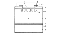
実施の形態にかかる炭化珪素半導体装置の製造方法によって作製(製造)される炭化珪素半導体装置の構造について、ショットバリアダイオード(以下、SiC−SBD)を例に説明する。図1は、実施の形態にかかる炭化珪素半導体装置の製造方法により製造される炭化珪素半導体装置の一例を示す断面図である。図1に示すように、実施の形態にかかる炭化珪素半導体装置において、炭化珪素(SiC)からなるn型半導体基板(以下、n型SiC基板とする)1のおもて面上には、n-型ドリフト領域となるn-型SiCエピタキシャル層2が設けられている。以下、n型SiC基板1およびn-型SiCエピタキシャル層2からなるn型SiCエピタキシャル基板の、n-型SiCエピタキシャル層2側の面をおもて面とし、n型SiC基板1側の面を裏面とする。
次に、n+型半導体領域7の不純物濃度および厚さと裏面電極(オーミック電極8および外部接続用電極層9)の剥離の有無との関係について説明する。図9は、実施例1にかかる炭化珪素半導体装置の裏面電極に対する剥離試験の結果を示す説明図である。まず、上述した実施の形態にかかる炭化珪素半導体装置の製造方法にしたがい、上記諸条件で図1に示すSiC−SBDを作製した(以下、実施例1−1,1−2とする)。具体的には、実施例1−1においては、製品完成後のn+型半導体領域7のボックスプロファイルの不純物濃度および厚さ(以降、単にn+型半導体領域7の不純物濃度および厚さとする)がそれぞれ8×10²⁰/cm3および200nmとなるように、上記加速エネルギーで第2イオン注入を行った。
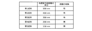
次に、n+型半導体領域7の厚さと裏面電極の剥離の有無との関係について説明する。図10は、実施例2にかかる炭化珪素半導体装置の裏面電極に対する剥離試験の結果を示す説明図である。実施例2としてn+型半導体領域7(図10においては高濃度不純物層と記載)の厚さの異なる第1〜5試料を作製した。第1〜5試料において、n+型半導体領域7の厚さは、それぞれ500nm、400nm、300nm、200nmおよび150nmとした。実施例2の、n+型半導体領域7の厚さ以外の条件は実施例1−1と同様である。実施例2において、第2イオン注入の加速エネルギーは実施例1−1と同様であり、第2イオン注入の多段注入数を増減させてn+型半導体領域7の厚さを変えている。すなわち、第2イオン注入の多段注入数を増やすことでn+型半導体領域7の厚さを厚くしており、第2イオン注入の多段注入数は、n+型半導体領域7の厚さの厚さが最も厚い第1試料が最も多く、n+型半導体領域7の厚さが最も薄い第5試料が最も少ない。第4試料は、実施例1−1に相当する。
2 n-型SiCエピタキシャル層
3 p+型半導体領域
4 層間絶縁膜
4a コンタクトホール
5 ショットキー電極
6 電極パッド
7 n+型半導体領域
8 オーミック電極
9 外部接続用電極層
11 カーボン保護膜
Claims (5)
- 炭化珪素からなる半導体基板の裏面に不純物を注入し、前記半導体基板の裏面の表面層に、前記半導体基板よりも不純物濃度が高い高濃度半導体領域を形成する第1工程と、
前記高濃度半導体領域の表面に金属電極を形成する第2工程と、
熱処理により、前記高濃度半導体領域と前記金属電極とのオーミックコンタクトを形成する第3工程と、
を含み、
前記第1工程では、
前記半導体基板の裏面に、30keV以上150keV以下の範囲の加速エネルギーで不純物を注入し、カーボン保護膜で保護した後、活性化熱処理し、前記カーボン保護膜を除去後に前記半導体基板の裏面を犠牲酸化し、当該犠牲酸化による犠牲酸化膜をバッファードフッ酸によるエッチングで除去することで、前記高濃度半導体領域の不純物濃度を1×10¹⁹/cm3以上8×1020/cm3以下とし、
前記高濃度半導体領域の厚さを200nm以下とし、
深さ方向に一様な不純物濃度プロファイルを有する前記高濃度半導体領域を形成することを特徴とする炭化珪素半導体装置の製造方法。 - 前記高濃度半導体領域の不純物濃度を4×10²⁰/cm3以下とすることを特徴とする
請求項1に記載の炭化珪素半導体装置の製造方法。 - 前記第1工程では、前記不純物として、アルミニウム、リン、砒素、窒素、ボロン、マ
グネシウムまたはガリウムを注入することを特徴とする請求項1または2に記載の炭化珪
素半導体装置の製造方法。 - 前記第2工程では、前記高濃度半導体領域の表面にニッケル層およびチタン層を順に形
成し、
前記第3工程では、熱処理により前記ニッケル層と前記高濃度半導体領域とを反応させ
て、前記金属電極としてニッケルシリサイド層を形成することを特徴とする請求項1〜3
のいずれか一つに記載の炭化珪素半導体装置の製造方法。 - 前記第2工程前に、前記半導体基板のおもて面側に、おもて面素子構造を形成する工程
をさらに含むことを特徴とする請求項1〜3のいずれか一つに記載の炭化珪素半導体装置
の製造方法。
Priority Applications (5)
| Application Number | Priority Date | Filing Date | Title |
|---|---|---|---|
| JP2013242367A JP6222771B2 (ja) | 2013-11-22 | 2013-11-22 | 炭化珪素半導体装置の製造方法 |
| CN201480061687.8A CN105765698A (zh) | 2013-11-22 | 2014-11-12 | 碳化硅半导体装置及碳化硅半导体装置的制造方法 |
| PCT/JP2014/079996 WO2015076166A1 (ja) | 2013-11-22 | 2014-11-12 | 炭化珪素半導体装置および炭化珪素半導体装置の製造方法 |
| DE112014004717.1T DE112014004717T5 (de) | 2013-11-22 | 2014-11-12 | Siliciumcarbid-Halbleitervorrichtung und Verfahren zum Herstellen einer Siliciumcarbid-Halbleitervorrichtung |
| US15/152,522 US10600921B2 (en) | 2013-11-22 | 2016-05-11 | Silicon carbide semiconductor device and method of manufacturing silicon carbide semiconductor device |
Applications Claiming Priority (1)
| Application Number | Priority Date | Filing Date | Title |
|---|---|---|---|
| JP2013242367A JP6222771B2 (ja) | 2013-11-22 | 2013-11-22 | 炭化珪素半導体装置の製造方法 |
Publications (2)
| Publication Number | Publication Date |
|---|---|
| JP2015103631A JP2015103631A (ja) | 2015-06-04 |
| JP6222771B2 true JP6222771B2 (ja) | 2017-11-01 |
Family
ID=53179433
Family Applications (1)
| Application Number | Title | Priority Date | Filing Date |
|---|---|---|---|
| JP2013242367A Active JP6222771B2 (ja) | 2013-11-22 | 2013-11-22 | 炭化珪素半導体装置の製造方法 |
Country Status (5)
| Country | Link |
|---|---|
| US (1) | US10600921B2 (ja) |
| JP (1) | JP6222771B2 (ja) |
| CN (1) | CN105765698A (ja) |
| DE (1) | DE112014004717T5 (ja) |
| WO (1) | WO2015076166A1 (ja) |
Families Citing this family (12)
| Publication number | Priority date | Publication date | Assignee | Title |
|---|---|---|---|---|
| JP6356428B2 (ja) * | 2014-02-17 | 2018-07-11 | 株式会社東芝 | 半導体装置およびその製造方法 |
| EP3067935A1 (en) * | 2015-03-10 | 2016-09-14 | ABB Technology AG | Power semiconductor rectifier with controllable on-state voltage |
| CN105470119B (zh) * | 2015-11-19 | 2018-09-11 | 泰科天润半导体科技(北京)有限公司 | 一种碳化硅器件的正面欧姆接触的加工方法 |
| JP6767705B2 (ja) * | 2016-04-28 | 2020-10-14 | パナソニックIpマネジメント株式会社 | 半導体素子 |
| CN107026075A (zh) * | 2016-08-31 | 2017-08-08 | 佛山芯光半导体有限公司 | 采用离子注入增强激光退火制备碳化硅欧姆接触的方法 |
| KR20180124459A (ko) * | 2017-05-12 | 2018-11-21 | 한국전기연구원 | 반도체와 금속 사이에 형성되는 오믹접촉 및 오믹접촉 형성방법 |
| US10615292B2 (en) | 2018-03-27 | 2020-04-07 | Hong Kong Applied Science And Technology Research Institute Co., Ltd. | High voltage silicon carbide Schottky diode flip chip array |
| JP7135443B2 (ja) * | 2018-05-29 | 2022-09-13 | 富士電機株式会社 | 炭化ケイ素半導体装置及びその製造方法 |
| CN109461768A (zh) * | 2018-10-31 | 2019-03-12 | 秦皇岛京河科学技术研究院有限公司 | 一种SiC结势垒肖特基二极管及其制造方法 |
| CN113228236B (zh) * | 2019-07-29 | 2024-08-09 | 富士电机株式会社 | 碳化硅半导体装置以及碳化硅半导体装置的制造方法 |
| US12211920B2 (en) * | 2021-04-13 | 2025-01-28 | Semiconductor Components Industries, Llc | Backside ohmic contacts for semiconductor devices |
| DE102022209805A1 (de) | 2022-09-19 | 2024-03-21 | Robert Bosch Gesellschaft mit beschränkter Haftung | Verfahren zum Erzeugen eines elektrischen Kontaktes, Halbleiteranordnung und Halbleiterbauelement |
Family Cites Families (38)
| Publication number | Priority date | Publication date | Assignee | Title |
|---|---|---|---|---|
| US6884644B1 (en) * | 1998-09-16 | 2005-04-26 | Cree, Inc. | Low temperature formation of backside ohmic contacts for vertical devices |
| US6803243B2 (en) * | 2001-03-15 | 2004-10-12 | Cree, Inc. | Low temperature formation of backside ohmic contacts for vertical devices |
| US6599644B1 (en) * | 2000-10-06 | 2003-07-29 | Foundation For Research & Technology-Hellas | Method of making an ohmic contact to p-type silicon carbide, comprising titanium carbide and nickel silicide |
| US6909119B2 (en) * | 2001-03-15 | 2005-06-21 | Cree, Inc. | Low temperature formation of backside ohmic contacts for vertical devices |
| JP4463448B2 (ja) * | 2001-09-07 | 2010-05-19 | パナソニック株式会社 | SiC基板及びSiC半導体素子の製造方法 |
| US7105875B2 (en) * | 2004-06-03 | 2006-09-12 | Wide Bandgap, Llc | Lateral power diodes |
| US7026669B2 (en) * | 2004-06-03 | 2006-04-11 | Ranbir Singh | Lateral channel transistor |
| JP4087368B2 (ja) * | 2004-09-21 | 2008-05-21 | 新電元工業株式会社 | SiC半導体装置の製造方法 |
| JP3914226B2 (ja) * | 2004-09-29 | 2007-05-16 | 株式会社東芝 | 高耐圧半導体装置 |
| JP4942134B2 (ja) * | 2005-05-20 | 2012-05-30 | 日産自動車株式会社 | 炭化珪素半導体装置の製造方法 |
| US8368165B2 (en) * | 2005-10-20 | 2013-02-05 | Siliconix Technology C. V. | Silicon carbide Schottky diode |
| JP2008135611A (ja) * | 2006-11-29 | 2008-06-12 | Denso Corp | 半導体装置の製造方法 |
| US7820534B2 (en) * | 2007-08-10 | 2010-10-26 | Mitsubishi Electric Corporation | Method of manufacturing silicon carbide semiconductor device |
| CN101842878B (zh) * | 2007-10-24 | 2012-05-23 | 松下电器产业株式会社 | 半导体元件及其制造方法 |
| US20090272982A1 (en) * | 2008-03-03 | 2009-11-05 | Fuji Electric Device Technology Co., Ltd. | Trench gate type semiconductor device and method of producing the same |
| US7851881B1 (en) * | 2008-03-21 | 2010-12-14 | Microsemi Corporation | Schottky barrier diode (SBD) and its off-shoot merged PN/Schottky diode or junction barrier Schottky (JBS) diode |
| CN101335201A (zh) * | 2008-05-30 | 2008-12-31 | 西安电子科技大学 | n型SiC半导体器件欧姆接触的制作方法 |
| CN102187464B (zh) | 2008-10-23 | 2014-04-16 | 本田技研工业株式会社 | 电极、半导体装置、及其制造方法 |
| US8188538B2 (en) * | 2008-12-25 | 2012-05-29 | Rohm Co., Ltd. | Semiconductor device and method of manufacturing semiconductor device |
| CN102396069B (zh) * | 2009-04-16 | 2014-05-07 | 三菱电机株式会社 | 碳化硅肖特基二极管的制造方法 |
| JP5525940B2 (ja) * | 2009-07-21 | 2014-06-18 | ローム株式会社 | 半導体装置および半導体装置の製造方法 |
| US9548206B2 (en) * | 2010-02-11 | 2017-01-17 | Cree, Inc. | Ohmic contact structure for group III nitride semiconductor device having improved surface morphology and well-defined edge features |
| JP5544918B2 (ja) | 2010-02-16 | 2014-07-09 | 住友電気工業株式会社 | 炭化珪素絶縁ゲート型半導体素子およびその製造方法 |
| KR101481878B1 (ko) | 2010-04-06 | 2015-01-12 | 미쓰비시덴키 가부시키가이샤 | 전력용 반도체 장치, 파워 모듈 및 전력용 반도체 장치의 제조 방법 |
| JP2012004269A (ja) | 2010-06-16 | 2012-01-05 | Sumitomo Electric Ind Ltd | 炭化珪素半導体装置の製造方法および炭化珪素半導体装置の製造装置 |
| CN103477439B (zh) | 2010-09-06 | 2014-12-10 | 松下电器产业株式会社 | 半导体装置及其制造方法 |
| WO2012140794A1 (ja) * | 2011-04-11 | 2012-10-18 | 新電元工業株式会社 | 炭化珪素半導体装置の製造方法 |
| JP5777455B2 (ja) * | 2011-09-08 | 2015-09-09 | 株式会社東芝 | 半導体装置および半導体装置の製造方法 |
| US8680587B2 (en) * | 2011-09-11 | 2014-03-25 | Cree, Inc. | Schottky diode |
| JP5869291B2 (ja) * | 2011-10-14 | 2016-02-24 | 富士電機株式会社 | 半導体装置 |
| JP6112698B2 (ja) | 2012-03-30 | 2017-04-12 | 富士電機株式会社 | 炭化珪素半導体素子及びその製造方法 |
| JP6053103B2 (ja) * | 2012-04-12 | 2016-12-27 | 富士電機株式会社 | ワイドバンドギャップ半導体装置およびその製造方法 |
| JP5966556B2 (ja) * | 2012-04-18 | 2016-08-10 | 富士電機株式会社 | 半導体デバイスの製造方法 |
| JP6253133B2 (ja) * | 2012-04-27 | 2017-12-27 | 富士電機株式会社 | 炭化珪素半導体装置の製造方法 |
| JP6206862B2 (ja) * | 2012-05-31 | 2017-10-04 | 富士電機株式会社 | 炭化珪素半導体装置および炭化珪素半導体装置の製造方法 |
| JP2014175470A (ja) * | 2013-03-08 | 2014-09-22 | Sumitomo Electric Ind Ltd | 炭化珪素半導体装置の製造方法 |
| JP6296445B2 (ja) * | 2014-02-10 | 2018-03-20 | ローム株式会社 | ショットキーバリアダイオード |
| US8962468B1 (en) * | 2014-04-23 | 2015-02-24 | United Silicon Carbide, Inc. | Formation of ohmic contacts on wide band gap semiconductors |
-
2013
- 2013-11-22 JP JP2013242367A patent/JP6222771B2/ja active Active
-
2014
- 2014-11-12 WO PCT/JP2014/079996 patent/WO2015076166A1/ja active Application Filing
- 2014-11-12 CN CN201480061687.8A patent/CN105765698A/zh active Pending
- 2014-11-12 DE DE112014004717.1T patent/DE112014004717T5/de not_active Withdrawn
-
2016
- 2016-05-11 US US15/152,522 patent/US10600921B2/en active Active
Also Published As
| Publication number | Publication date |
|---|---|
| US10600921B2 (en) | 2020-03-24 |
| WO2015076166A1 (ja) | 2015-05-28 |
| US20160254393A1 (en) | 2016-09-01 |
| JP2015103631A (ja) | 2015-06-04 |
| CN105765698A (zh) | 2016-07-13 |
| DE112014004717T5 (de) | 2016-07-07 |
Similar Documents
| Publication | Publication Date | Title |
|---|---|---|
| JP6222771B2 (ja) | 炭化珪素半導体装置の製造方法 | |
| CN101647093B (zh) | 制造半导体装置的方法和半导体装置 | |
| JP7103444B2 (ja) | 炭化珪素半導体素子 | |
| EP2933826A2 (en) | Semiconductor device and method for producing the same | |
| CN104303269B (zh) | 碳化硅半导体装置的制造方法 | |
| CN104126219B (zh) | SiC半导体器件及其制造方法 | |
| JP2009049198A (ja) | 半導体装置およびその製造方法 | |
| EP2325872A1 (en) | Bipolar semiconductor device and method for manufacturing same | |
| JP2017168602A (ja) | 半導体装置および半導体装置の製造方法 | |
| JP6160541B2 (ja) | 炭化珪素半導体装置の製造方法 | |
| JP6686581B2 (ja) | 炭化珪素半導体素子および炭化珪素半導体素子の製造方法 | |
| JP2013058668A (ja) | 半導体素子及びその製造方法 | |
| JP2019029501A (ja) | 半導体装置および半導体装置の製造方法 | |
| CN105493245A (zh) | 碳化硅半导体元件以及碳化硅半导体元件的制造方法 | |
| CN107204363A (zh) | 碳化硅半导体装置及碳化硅半导体装置的制造方法 | |
| JP6253133B2 (ja) | 炭化珪素半導体装置の製造方法 | |
| JP6648574B2 (ja) | 炭化珪素半導体装置の製造方法 | |
| JP6395299B2 (ja) | 炭化珪素半導体素子及び炭化珪素半導体素子の製造方法 | |
| JP2018082056A (ja) | 半導体装置および半導体装置の製造方法 | |
| JP6808952B2 (ja) | 炭化珪素半導体装置の製造方法 | |
| JP5921089B2 (ja) | エピタキシャルウエハの製造方法及び半導体装置の製造方法 | |
| US9887270B2 (en) | Silicon carbide semiconductor device and method of manufacturing silicon carbide semiconductor device | |
| JP6724444B2 (ja) | 炭化珪素半導体素子および炭化珪素半導体素子の製造方法 | |
| JP2019169486A (ja) | 半導体装置及びその製造方法 | |
| JP2018006564A (ja) | 半導体装置および半導体装置の製造方法 |
Legal Events
| Date | Code | Title | Description |
|---|---|---|---|
| A521 | Request for written amendment filed |
Free format text: JAPANESE INTERMEDIATE CODE: A523 Effective date: 20160809 |
|
| A621 | Written request for application examination |
Free format text: JAPANESE INTERMEDIATE CODE: A621 Effective date: 20160905 |
|
| A131 | Notification of reasons for refusal |
Free format text: JAPANESE INTERMEDIATE CODE: A131 Effective date: 20161122 |
|
| A521 | Request for written amendment filed |
Free format text: JAPANESE INTERMEDIATE CODE: A523 Effective date: 20170120 |
|
| A131 | Notification of reasons for refusal |
Free format text: JAPANESE INTERMEDIATE CODE: A131 Effective date: 20170516 |
|
| A521 | Request for written amendment filed |
Free format text: JAPANESE INTERMEDIATE CODE: A523 Effective date: 20170718 |
|
| TRDD | Decision of grant or rejection written | ||
| A01 | Written decision to grant a patent or to grant a registration (utility model) |
Free format text: JAPANESE INTERMEDIATE CODE: A01 Effective date: 20170905 |
|
| A61 | First payment of annual fees (during grant procedure) |
Free format text: JAPANESE INTERMEDIATE CODE: A61 Effective date: 20170929 |
|
| R150 | Certificate of patent or registration of utility model |
Ref document number: 6222771 Country of ref document: JP Free format text: JAPANESE INTERMEDIATE CODE: R150 |
|
| R250 | Receipt of annual fees |
Free format text: JAPANESE INTERMEDIATE CODE: R250 |
|
| R250 | Receipt of annual fees |
Free format text: JAPANESE INTERMEDIATE CODE: R250 |
|
| R250 | Receipt of annual fees |
Free format text: JAPANESE INTERMEDIATE CODE: R250 |
|
| R250 | Receipt of annual fees |
Free format text: JAPANESE INTERMEDIATE CODE: R250 |
|
| R250 | Receipt of annual fees |
Free format text: JAPANESE INTERMEDIATE CODE: R250 |