JP6098224B2 - Surface mount type piezoelectric oscillator - Google Patents
Surface mount type piezoelectric oscillator Download PDFInfo
- Publication number
- JP6098224B2 JP6098224B2 JP2013035265A JP2013035265A JP6098224B2 JP 6098224 B2 JP6098224 B2 JP 6098224B2 JP 2013035265 A JP2013035265 A JP 2013035265A JP 2013035265 A JP2013035265 A JP 2013035265A JP 6098224 B2 JP6098224 B2 JP 6098224B2
- Authority
- JP
- Japan
- Prior art keywords
- base
- external terminals
- adjustment
- long side
- piezoelectric vibration
- Prior art date
- Legal status (The legal status is an assumption and is not a legal conclusion. Google has not performed a legal analysis and makes no representation as to the accuracy of the status listed.)
- Active
Links
- 239000000463 material Substances 0.000 claims description 28
- 239000000919 ceramic Substances 0.000 claims description 26
- 238000003860 storage Methods 0.000 claims description 23
- 239000000758 substrate Substances 0.000 claims description 21
- 238000005259 measurement Methods 0.000 claims description 17
- 230000005284 excitation Effects 0.000 claims description 4
- 238000010030 laminating Methods 0.000 claims description 2
- 239000010410 layer Substances 0.000 description 31
- 229910052751 metal Inorganic materials 0.000 description 18
- 239000002184 metal Substances 0.000 description 18
- 239000013078 crystal Substances 0.000 description 17
- PXHVJJICTQNCMI-UHFFFAOYSA-N Nickel Chemical compound [Ni] PXHVJJICTQNCMI-UHFFFAOYSA-N 0.000 description 14
- 229910000679 solder Inorganic materials 0.000 description 10
- 230000010355 oscillation Effects 0.000 description 9
- 239000000853 adhesive Substances 0.000 description 8
- 230000001070 adhesive effect Effects 0.000 description 8
- 239000011347 resin Substances 0.000 description 8
- 229920005989 resin Polymers 0.000 description 8
- PCHJSUWPFVWCPO-UHFFFAOYSA-N gold Chemical compound [Au] PCHJSUWPFVWCPO-UHFFFAOYSA-N 0.000 description 7
- 229910052737 gold Inorganic materials 0.000 description 7
- 239000010931 gold Substances 0.000 description 7
- 229910052759 nickel Inorganic materials 0.000 description 7
- 238000007789 sealing Methods 0.000 description 7
- 230000002787 reinforcement Effects 0.000 description 6
- 238000000034 method Methods 0.000 description 5
- 239000010453 quartz Substances 0.000 description 5
- 239000003566 sealing material Substances 0.000 description 5
- VYPSYNLAJGMNEJ-UHFFFAOYSA-N silicon dioxide Inorganic materials O=[Si]=O VYPSYNLAJGMNEJ-UHFFFAOYSA-N 0.000 description 5
- 101100393868 Arabidopsis thaliana GT11 gene Proteins 0.000 description 4
- 238000005219 brazing Methods 0.000 description 4
- 229910010293 ceramic material Inorganic materials 0.000 description 4
- 239000010408 film Substances 0.000 description 4
- 238000004519 manufacturing process Methods 0.000 description 4
- 238000007747 plating Methods 0.000 description 4
- VYZAMTAEIAYCRO-UHFFFAOYSA-N Chromium Chemical compound [Cr] VYZAMTAEIAYCRO-UHFFFAOYSA-N 0.000 description 3
- ZOKXTWBITQBERF-UHFFFAOYSA-N Molybdenum Chemical compound [Mo] ZOKXTWBITQBERF-UHFFFAOYSA-N 0.000 description 3
- BQCADISMDOOEFD-UHFFFAOYSA-N Silver Chemical compound [Ag] BQCADISMDOOEFD-UHFFFAOYSA-N 0.000 description 3
- 229910052804 chromium Inorganic materials 0.000 description 3
- 239000011651 chromium Substances 0.000 description 3
- 238000001465 metallisation Methods 0.000 description 3
- 229910052750 molybdenum Inorganic materials 0.000 description 3
- 239000011733 molybdenum Substances 0.000 description 3
- 230000002093 peripheral effect Effects 0.000 description 3
- 229920001296 polysiloxane Polymers 0.000 description 3
- 229910052709 silver Inorganic materials 0.000 description 3
- 239000004332 silver Substances 0.000 description 3
- 239000010409 thin film Substances 0.000 description 3
- WFKWXMTUELFFGS-UHFFFAOYSA-N tungsten Chemical compound [W] WFKWXMTUELFFGS-UHFFFAOYSA-N 0.000 description 3
- 229910052721 tungsten Inorganic materials 0.000 description 3
- 239000010937 tungsten Substances 0.000 description 3
- PNEYBMLMFCGWSK-UHFFFAOYSA-N aluminium oxide Inorganic materials [O-2].[O-2].[O-2].[Al+3].[Al+3] PNEYBMLMFCGWSK-UHFFFAOYSA-N 0.000 description 2
- 230000000694 effects Effects 0.000 description 2
- 238000005516 engineering process Methods 0.000 description 2
- 239000011521 glass Substances 0.000 description 2
- 238000009413 insulation Methods 0.000 description 2
- 238000005304 joining Methods 0.000 description 2
- 230000003014 reinforcing effect Effects 0.000 description 2
- 239000004593 Epoxy Substances 0.000 description 1
- 229910001111 Fine metal Inorganic materials 0.000 description 1
- 229910013641 LiNbO 3 Inorganic materials 0.000 description 1
- 230000002411 adverse Effects 0.000 description 1
- 239000011162 core material Substances 0.000 description 1
- 238000010586 diagram Methods 0.000 description 1
- 238000010894 electron beam technology Methods 0.000 description 1
- 238000000605 extraction Methods 0.000 description 1
- 239000000945 filler Substances 0.000 description 1
- 238000010304 firing Methods 0.000 description 1
- 229910000833 kovar Inorganic materials 0.000 description 1
- 238000003475 lamination Methods 0.000 description 1
- 238000012986 modification Methods 0.000 description 1
- 230000004048 modification Effects 0.000 description 1
- 231100000989 no adverse effect Toxicity 0.000 description 1
- 238000007639 printing Methods 0.000 description 1
- 230000000717 retained effect Effects 0.000 description 1
- 239000000523 sample Substances 0.000 description 1
- 238000005476 soldering Methods 0.000 description 1
- 238000004544 sputter deposition Methods 0.000 description 1
- 239000002344 surface layer Substances 0.000 description 1
- 238000001771 vacuum deposition Methods 0.000 description 1
Images


Landscapes
- Oscillators With Electromechanical Resonators (AREA)
Description
本発明は、絶縁性のベース上に圧電振動素子と集積回路素子が実装された表面実装型圧電発振器に関するものであって、特に表面実装型圧電発振器のパッケージ構造を改善するものである。 The present invention relates to a surface-mount piezoelectric oscillator in which a piezoelectric vibration element and an integrated circuit element are mounted on an insulating base, and particularly to improve the package structure of a surface-mount piezoelectric oscillator.
水晶振動板等の圧電振動素子を用いた圧電発振器は、安定して精度の高い発振周波数を得ることができるため、電子機器等の基準周波数源として多種の分野で使用されている。表面実装型圧電発振器では、絶縁性のベースとしてセラミック多層基板を用い、当該ベースの収納部に発振回路用等の集積回路素子を配置するとともに、当該集積回路素子の上方に水晶振動板を支持固定し、蓋により気密封止を行ったものである。このような構成はC−MOS等のインバータ増幅器(発振用増幅器)を内蔵したワンチップの集積回路素子のカスタム化により比較的部品点数が少なく、シンプルな構成であり、低コスト化に寄与している。 A piezoelectric oscillator using a piezoelectric vibration element such as a quartz diaphragm can stably obtain a highly accurate oscillation frequency, and is therefore used in various fields as a reference frequency source for electronic devices and the like. In a surface-mount piezoelectric oscillator, a ceramic multilayer substrate is used as an insulating base, and an integrated circuit element for an oscillation circuit is arranged in a housing portion of the base, and a crystal diaphragm is supported and fixed above the integrated circuit element. And hermetically sealed with a lid. Such a configuration has a relatively small number of parts due to customization of a one-chip integrated circuit element incorporating an inverter amplifier (oscillation amplifier) such as a C-MOS, contributing to cost reduction. Yes.
このような表面実装型圧電発振器では、ワイヤボンディングに比較して小型化低背化が実現できることから、特許文献1にも示すように、セラミックのベースの収納部の配線パターンに集積回路素子のパッドを、金等の金属バンプを用いて超音波熱圧着によるフリップチップボンディング接合されることが近年多くなっている。
In such a surface mount type piezoelectric oscillator, since it can be reduced in size and height as compared with wire bonding, as shown in
ところで、上述のような表面実装型圧電発振器をはんだにより接合し搭載する回路基板には様々な材料のものがある。この材料によってはパッケージと回路基板との間で熱膨張差が生じて、パッケージと回路基板を接合するはんだにも応力が生じるため、クラックが発生することがある。特に、パッケージとしてアルミナ等のセラミック材料を用い、回路基板としてガラスエポキシ基板を用いた組み合わせ構成であれば、パッケージの熱膨張係数に対して回路基板の熱膨張係数が大きくなり、はんだから疲労破壊が生じやすくなる。また当該パッケージと回路基板とに衝撃が加わると、はんだクラック部分から剥離が生じるといった問題点もあった。 By the way, there are various materials for circuit boards on which the surface-mounted piezoelectric oscillator as described above is mounted by soldering. Depending on this material, a difference in thermal expansion occurs between the package and the circuit board, and stress is also generated in the solder joining the package and the circuit board, so that cracks may occur. In particular, when a ceramic material such as alumina is used as the package and a glass epoxy substrate is used as the circuit board, the thermal expansion coefficient of the circuit board is larger than the thermal expansion coefficient of the package, and fatigue damage from solder is caused. It tends to occur. Further, when an impact is applied to the package and the circuit board, there is a problem that peeling occurs from a solder crack portion.
このようなはんだクラックの問題については、表面実装型圧電発振器の小型化に伴って外部端子の面積も小さくなり対応が困難になってきている。特に、圧電振動子に比べて、機能する外部端子の数が多く、かつその機能する各外部端子の役割も多様となっている圧電発振器では、外部端子の面積だけでなく、各外部端子の役割に応じた配置にも制限が加わるため、より対応が困難になってきているのが現状である。 With respect to such a solder crack problem, it is becoming difficult to cope with the reduction in the area of the external terminal as the surface-mounted piezoelectric oscillator is downsized. In particular, in a piezoelectric oscillator that has a large number of functioning external terminals and a variety of roles for each functioning external terminal as compared to a piezoelectric vibrator, not only the area of the external terminal but also the role of each external terminal. Since there is a restriction on the arrangement according to the current situation, it is becoming more difficult to deal with the situation.
そこで、上記課題を解決するために、本発明は、小型化に対応させながら、はんだクラックの対応も行えるより信頼性の高い表面実装型圧電発振器を提供することを目的とする。 Accordingly, in order to solve the above-described problems, an object of the present invention is to provide a more reliable surface-mount piezoelectric oscillator that can cope with solder cracks while reducing the size.
上記の目的を達成するために、本発明の特許請求項1に示すように、矩形状のセラミック基板が積層されて収納部と外装部とが構成され絶縁性のベースと、前記ベースの収納部に搭載される集積回路素子と圧電振動素子とを有しており、前記ベースの外装部の底面には、4角と長辺中央に6つの外部端子が形成され、前記4角の外部端子が実装外部端子として構成され、前記長辺の一対の外部端子が、集積回路素子のデータ調整用の調整外部端子として構成されるとともに、前記ベースの外装部の底面の長辺から離隔した状態で形成されており、前記調整外部端子の一方がデータ入出力端子として構成され、前記調整外部端子の他方がデータ制御端子として構成されており、前記ベースの外装部の長辺方向の側面には、前記圧電振動素子の励振電極と直接接続された一対の圧電振動素子の特性測定用の測定外部端子が構成されるとともに、前記ベースの外装部の底面の長辺から離隔した状態で形成されており、前記実装外部端子に接合材を用いて回路基板の配線パターンへ接合するとともに、前記一対の調整外部端子にも接合材を用いて回路基板のグランド用配線パターンのみへ接合することを特徴とする。
In order to achieve the above object, as shown in
上記構成により、表面実装型圧電発振器の製造段階でのみ利用し、製品化にはユーザー側で不要である前記調整外部端子は、回路基板のグランド用配線パターンに接合材を用いて接続しているので、この調整外部端子に対して不要な電圧が加わることがなくなるため、集積回路素子のデータが書き換わることがなくなる。そして、製品化された表面実装型圧電発振器としてユーザー側で必要な実装外部端子だけでなく、前記調整外部端子を回路基板へ搭載する際の接合補強用の外部端子として利用できる。つまり、製造時にはデータの入出力が可能な状態で不安定な調整外部端子であっても、当該調整外部端子を回路基板へ搭載する際にはデータを書き換えられない安定した接合補強用の外部端子として再利用できる。別途接合補強用の外部端子を設ける必要もなく、かつそれぞれ機能する各外部端子の役割を変更することもなく、規格に応じた外部端子の配置的な制限にも対応することができる。以上により、小型化に対応させながら、はんだクラックの対応も行えるより信頼性の高い外部端子の接続構造が得られる。 With the above configuration, the adjustment external terminal, which is used only at the manufacturing stage of the surface-mount type piezoelectric oscillator and is not necessary for the user to commercialize, is connected to the ground wiring pattern of the circuit board using a bonding material. Therefore, an unnecessary voltage is not applied to the adjustment external terminal, and the data of the integrated circuit element is not rewritten. And as a surface-mount type piezoelectric oscillator that has been commercialized, it can be used not only as a mounting external terminal necessary on the user side, but also as an external terminal for bonding reinforcement when the adjustment external terminal is mounted on a circuit board. In other words, even if the adjustment external terminal is unstable in a state where data can be input / output at the time of manufacture, the external terminal for stable joint reinforcement that cannot be rewritten when the adjustment external terminal is mounted on the circuit board Can be reused as It is not necessary to provide an external terminal for reinforcing the connection separately, and the role of each functioning external terminal is not changed, and it is possible to deal with restrictions on arrangement of the external terminals according to the standard. As described above, it is possible to obtain a more reliable external terminal connection structure that can cope with solder cracks while reducing the size.
また、前記ベースの外装部の底面の調整外部端子と、前記ベースの外装部の長辺方向の側面中央の測定外部端子とは、前記ベースの外装部の底面の長辺から離隔した状態で形成されているため、表面実装型圧電発振器の小型化に対応させながら、各機能を有する調整外部端子と測定外部端子とでお互いに干渉することがなくなり、発振器を製造する際や製品化された後にも悪影響を与えることがない。加えて、各機能を有するお互いの外部端子の配置的な制限にも対応することができる。 In addition, the adjustment external terminal on the bottom surface of the exterior portion of the base and the measurement external terminal in the center of the side surface in the long side direction of the exterior portion of the base are formed in a state separated from the long side of the bottom surface of the exterior portion of the base. Therefore, while adjusting to the miniaturization of surface-mounted piezoelectric oscillators, the adjustment external terminals and measurement external terminals that have each function do not interfere with each other. There is no adverse effect. In addition, it is possible to deal with restrictions on arrangement of external terminals having functions.
また、上記構成において、前記ベースは、4角と長辺中央とにキャスタレーションが形成された3層以上の矩形状のセラミック基板が積層されて構成されており、
前記4つの実装外部端子は、それぞれの前記4角のキャスタレーションを介して底面層のセラミック基板の側面にも引き回し電極が形成され、
前記一対の測定外部端子は、前記長辺中央のキャスタレーションを介して中間層のセラミック基板の側面のみに形成されていてもよい。
この構成では、上述の構成に加えて、前記4角のキャスタレーションに形成された引き回し電極にも接合材が這い上がり、回路基板へ搭載する際の接合補強と接合材の塗布状態を認識するための部分として利用できる。また測定外部端子はセラミック基板の上面との絶縁を確保することができるため、メタライズの封止領域をセラミック基板に構成した場合にも短絡することがない。
Further, in the above configuration, the base is configured by laminating three or more rectangular ceramic substrates in which castellations are formed at the four corners and the center of the long side,
The four mounting external terminals are routed electrodes on the side surface of the ceramic substrate of the bottom layer through the four corner castellations,
The pair of measurement external terminals may be formed only on the side surface of the ceramic substrate of the intermediate layer via the castellation at the center of the long side.
In this configuration, in addition to the above-described configuration, the bonding material also crawls up on the lead-out electrodes formed in the square castellations so that the bonding reinforcement and the application state of the bonding material when mounted on the circuit board are recognized. Available as part of Further, since the measurement external terminal can ensure insulation from the upper surface of the ceramic substrate, there is no short circuit even when the metallized sealing region is formed on the ceramic substrate.
以上のように、本発明は、小型化に対応させながら、はんだクラックの対応も行え、より信頼性の高い表面実装型圧電発振器を提供することを目的とする。 As described above, an object of the present invention is to provide a highly reliable surface-mount piezoelectric oscillator that can deal with solder cracks while accommodating downsizing.
以下、本発明による好ましい実施形態につきセラミック多層基板のベースを用いた表面実装型水晶発振器(表面実装型圧電発振器)を例にとり図面とともに説明する。 Hereinafter, a preferred embodiment of the present invention will be described with reference to the drawings by taking a surface-mounted crystal oscillator (surface-mounted piezoelectric oscillator) using a ceramic multilayer base as an example.
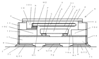
表面実装型水晶発振器6は、上部が開口した凹部を有する絶縁性のセラミック多層基板からなるベース1(以下、ベースと称する)と、当該ベースの中に収納される集積回路素子2と、同じく当該ベース中の上部に収納される圧電振動素子3と、ベースの開口部に接合される蓋4とからなる。この表面実装型水晶発振器では、ベース1と蓋4とが封止材5を用いて接合されて気密封止され、表面実装型水晶発振器6が構成されている。以下、この表面実装型水晶発振器6の各構成について説明する。
The surface-
セラミック多層基板のベース1は全体として直方体で、最下層であるアルミナ等のセラミック材料からなる平面視矩形状の一枚板の底部11と、この底部11上に積層した中間層のセラミック材料の平面視枠形状の堤部12と、最上層のセラミック材料の平面視枠形状の堤部13とから構成され、収納部10を有する断面凹形の箱状体(外装部14)に形成されている。収納部10は第1の収納部10a(下部収納部)と第2の収納部10b(上部収納部)からなり、それぞれ集積回路素子2と圧電振動素子3が収納される。なお、セラミック多層基板として本形態のように3層構造のベースに限定されるものではなく、ベースの収納部の構造に応じて4層以上で構成してもよい。
The
前記セラミック多層基板のベース1の最上層である堤部13の上面(端面)は平坦であり、後述する蓋4との接合領域(金属膜)13aである。この接合領域13aは、タングステンあるいはモリブデン等のメタライズ材料からなるメタライズ層と、このメタライズ層に積層されたニッケル層と、このニッケル層に積層された金層とから構成される。タングステンあるいはモリブデンは厚膜印刷技術を活用してメタライズ技術によりセラミック焼成時に一体的に形成され、メタライズ層上にニッケル層、金層の順でメッキ形成される。
The upper surface (end surface) of the
ベース1の外周壁の4角には上下方向に伸長するキャスタレーションC1,C2,C3,C4がそれぞれ形成され、ベース1の外周壁の長辺中央の一部には上下方向に伸長する半長円状のキャスタレーションC5,C6がそれぞれ形成されている。当該キャスタレーションはベースの外周壁に対して円弧状あるいは半長円状の切り欠きが上下方向に形成された構成である。なお、前記接合領域13aはベースの堤部12,13を上下に貫通接続する図示しない導電ビアやキャスタレーション上部に形成された図示しない配線パターンのいずれか少なくとも一方により、ベース底面側に形成された外部端子パッドGT2の一部に電気的に導出されている。当該外部端子パッドGT2をアース接続することにより、後述する金属製の蓋が接合領域13a、導電ビアやキャスタレーション上部の配線パターンなどを介して接地され、表面実装型水晶発振器の電磁気的なシールド効果を得ることができる。
Casters C1, C2, C3, and C4 that extend in the vertical direction are formed on the four corners of the outer peripheral wall of the
ベース1の内部において、下方面には前記堤部(側壁部)12により構成され、集積回路素子2を収納する第1の収納部10aが形成され、当該第1の収納部の底面から上部に突き出し、後述する圧電振動素子の端部を保持する保持台10cと、前記第1の収納部を介して前記保持台と対向位置する枕部10dが形成されている。また前記第1の収納部10aの上方には前記堤部(側壁部)13により構成された第2の収納部10bが形成されている。
Inside the
前記セラミック多層基板のベース1の最下層である底部11の上面(前記第1の収納部10aの内底面)には、図4に示すように、後述する集積回路素子2と接続される複数の配線パターンH1が並んで形成されている。
On the upper surface of the bottom 11 (the inner bottom surface of the first storage portion 10a), which is the lowest layer of the
前記セラミック多層基板のベース1の最下層である底部11の下面(ベースの外装部の底面)には、4角と長辺中央に6つの外部端子GTが形成されている。具体的には図2に示すように、前記4角の外部端子が実装外部端子GT1,GT2,GT3,GT4として構成される。実装外部端子GT1,GT2,GT3,GT4は、それぞれ4角のキャスタレーションC1,C2,C3,C4を介してベース1の最下層である底部11の側面(底面層のセラミック基板の側面)にも引き回し電極GT11,GT21,GT31,GT41が形成されている。例えば、本形態では、実装外部端子GT1は電源端子(VCC)、実装外部端子GT2は出力端子(OUT)、実装外部端子GT3は接地端子(GND)、実装外部端子GT4は出力制御端子(OE)や周波数制御端子(VCONT)、NC端子などいずれかとして構成した。
Six external terminals GT are formed at the four corners and at the center of the long side on the lower surface of the bottom portion 11 (the bottom surface of the base exterior portion) which is the lowermost layer of the
前記長辺中央の一対の外部端子が後述する集積回路素子2のデータ調整用の調整外部端子GT7,GT8として構成される。例えば、本形態では、調整用外部端子GT7はデータ入出力端子(IO)、調整用外部端子GT8はデータ制御端子(CS)として構成した。
調整外部端子GT7,GT8は、底部11の下面(ベースの外装部の底面)の長辺15,16から底部11の中心方向へ離隔した状態で形成されている。
A pair of external terminals in the center of the long side are configured as adjustment external terminals GT7 and GT8 for data adjustment of the
The adjustment external terminals GT7 and GT8 are formed in a state of being separated from the
なお、実装外部端子GT1,GT2,GT3,GT4は、引き回し電極GT11,GT21,GT31,GT41を介して、複数の配線パターンH1のいずれかに電気的に導出されている。調整外部端子GT7,GT8は、上部に貫通接続する導電ビアV1,V2を介して、複数の配線パターンH1のいずれかに電気的に導出されている。 Note that the mounting external terminals GT1, GT2, GT3, and GT4 are electrically derived to one of the plurality of wiring patterns H1 via the routing electrodes GT11, GT21, GT31, and GT41. The adjustment external terminals GT7 and GT8 are electrically led to one of the plurality of wiring patterns H1 through conductive vias V1 and V2 penetratingly connected to the upper part.
前記セラミック多層基板のベース1の中間層である堤部12の上面(前記第2の収納部10bの底面)には、後述する圧電振動素子3を搭載する保持台10cが形成されており、その上面には後述する圧電振動素子3と接続される一対の配線パターンH2が形成されている。前記保持台10cは堤部12の一部が収納部10の方に突出することで構成されている。この配線パターンH2は、下部に貫通接続する導電ビアV3を介して、複数の配線パターンH1のいずれかに電気的に導出されている。
On the upper surface of the bank portion 12 (the bottom surface of the second storage portion 10b), which is an intermediate layer of the
セラミック多層基板のベース1の中間層である堤部12の一対の長辺中央には、キャスタレーションC5,C6の一部がそれぞれ形成されている。これら堤部12の長辺中央のキャスタレーションC5,C6の上部には、配線パターンH2と接続され、後述する圧電振動素子3の励振電極31,32と直接接続された一対の圧電振動素子の特性測定用の測定外部端子GT5,GT6が構成される。つまり、測定外部端子GT5,GT6は中間層である堤部12の上面にのみ形成されているので、底部11の下面(ベースの外装部の底面)の長辺15,16と、最上層である堤部13の接合領域(金属膜)13aとから離隔した状態で形成されている。なお、前記一対の測定外部端子GT5,GT6に対して、圧電振動素子特性装置のコンタクトプローブを接触することで後述する圧電振動素子3単独の特性を測定することができる。
Part of castellations C5 and C6 are formed at the center of a pair of long sides of the
以上のような構成のベース1は周知のセラミック積層技術やメタライズ技術を用いて形成される。実装外部端子GT1,GT2,GT3,GT4、引き回し電極GT11,GT21,GT31,GT41、測定外部端子GT5,GT6、調整外部端子GT7,GT8、配線パターンH1、配線パターンH2は、接合領域13aの形成と同様にタングステンあるいはモリブデン等によるメタライズ層の上面にニッケルメッキ層、金メッキ層の各層が形成された構成である。
The
第1の収納部10aの内底面に搭載される集積回路素子2は、C−MOSなどのインバータ増幅器(発振用増幅器)を内蔵したワンチップの集積回路素子であり、図5に示すように、圧電振動素子3とともに発振回路を構成する。集積回路素子2の底面側には複数のパッドPが形成されている。当該集積回路素子2は、例えば金などの金属バンプCを介して、集積回路素子2の複数のパッドPとベース1に形成された配線パターンH1とを例えばFCBにより接続される。なお、本形態では、金属バンプにより接合した構成を例にしているが、金属ワイヤバンプを用いてもよい。
The
集積回路素子2の上方で、収納部10の同一空間である第2の収納部10bには所定の間隔を持って圧電振動素子3が搭載される。圧電振動素子3は例えば矩形状のATカット水晶振動板であり、その表裏面に対向して一対の矩形状励振電極31,32とこれらの引出電極が形成されている。これらの電極は、例えば、クロムまたはニッケルの下地電極層と、銀または金の中間電極層と、クロムまたはニッケルの上部電極層とから構成された積層薄膜、クロムやニッケルの下地電極層と、銀または金の上部電極層とから構成された積層薄膜である。これら各電極は真空蒸着法やスパッタリング法等の薄膜形成手段により形成することができる。
Above the
圧電振動素子3とベース1との接合は、例えばペースト状であり銀フィラー等の金属微小片を含有するシリコーン系の導電樹脂接着剤(導電性接合材)Sを用いている。図1に示すように、導電性樹脂接着剤Sは、一対の配線パターンH2のうちの一部の上面に塗布されるとともに、導電性樹脂接着剤Sを圧電振動素子3と保持台10cの間に介在させ硬化させることで、お互いを電気的機械的に接合している。以上により、圧電振動素子3の一端部をベース1の第1の収納部10aの底面から隙間を設けながら、圧電振動素子3の対向する他端部をベースの保持台10cに接合して、片持ち保持される。なお、本形態では、シリコーン系の導電樹脂接着剤により接合した構成を例にしているが、この導電性接合材として他の導電性樹脂接着剤や金属バンプ、金属メッキバンプなどを用いてもよい。
The
ベース1を気密封止する蓋4は、例えば、コバール等からなるコア材に金属ろう材(封止材)が形成された構成である。この金属ろう材からなる封止材5がベース1の接合領域(金属膜)13aと接合される構成となる。金属製の蓋4の平面視外形はセラミックベースの当該外形とほぼ同じであるか、若干小さい構成となっている。
The
収納部10に集積回路素子2と圧電振動素子3が格納されたベース1の接合領域13aに対して金属製の蓋4にて被覆し、金属製の蓋4の封止材5とベースの接合領域13aを溶融硬化させ、気密封止を行うことで表面実装型水晶発振器6の完成となる。
The joint area 13a of the
このように構成された表面実装型水晶発振器6は、図1に示すように、回路基板7の配線パターン71に対してはんだなどの接合材8を用いて接合される。つまり、実装外部端子GT1,GT2,GT3,GT4(図1ではGT1,GT2のみ図示)に接合材8を用いて回路基板7の配線パターン71へ接合する。調整外部端子GT7,GT8に(図1ではGT8のみ図示)も接合材8を用いて回路基板7のグランド用配線パターン72へ接合する。
As shown in FIG. 1, the surface-mount
上記実施形態により、製品化された表面実装型水晶発振器6としてユーザー側で必要な実装外部端子GT1,GT2,GT3,GT4だけでなく、表面実装型水晶発振器の製造段階でのみ利用し、製品化にはユーザー側で不要である調整外部端子GT7,GT8を回路基板7へ搭載する際の接合補強用の外部端子として利用できる。しかも、調整外部端子GT7,GT8は、回路基板7のグランド用配線パターン72に接合材8を用いて接続しているので、調整外部端子GT7,GT8に対して不要な電圧が加わることがなくなるので集積回路素子2のデータが書き換わることがなくなる。
According to the above embodiment, not only the mounting external terminals GT1, GT2, GT3 and GT4 necessary on the user side as the surface mounted
本形態では、調整用外部端子GT7はデータ入出力端子(IO)、調整用外部端子GT8はデータ制御端子(CS)として構成されているので、データ制御端子(CS)に特定の電圧を加えることで、データ入出力端子(IO)に対して特定の調整データを入力できるように構成されている。そこで、少なくとも前記データ制御端子(CS)に対して外部から特定の電圧が加わらないように、回路基板7のグランド用配線パターン72に接合することで、データ入出力端子(IO)に不要な調整データが入力されることが一切なくなる。
In this embodiment, the adjustment external terminal GT7 is configured as a data input / output terminal (IO), and the adjustment external terminal GT8 is configured as a data control terminal (CS). Therefore, a specific voltage is applied to the data control terminal (CS). Thus, specific adjustment data can be input to the data input / output terminal (IO). Therefore, unnecessary adjustment is not made to the data input / output terminal (IO) by bonding to the ground wiring pattern 72 of the
つまり、小型化された表面実装型水晶発振器であっても、製品化後に必要な実装外部端子GT1,GT2,GT3,GT4だけでなく、製造時にはデータの入出力が可能な状態で不安定な調整外部端子GT7,GT8であっても、調整外部端子GT7,GT8を回路基板へ搭載する際にはデータを書き換えられない安定した接合補強用の外部端子として再利用することができるようになる。実装外部端子や調整外部端子以外に別途接合補強用の外部端子を設ける必要がない。また、それぞれ機能する各実装外部端子や調整外部端子の役割を変更することもなく、規格に応じた外部端子の配置的な制限にも対応することができる。以上により、小型化に対応させながら、はんだクラックの対応も行え、より信頼性の高い外部端子の接続構造が得られる。また、調整外部端子GT7,GT8を、底部11の下面(ベースの外装部の底面)の長辺15,16の中央の位置にそれぞれ形成している。このため、回路基板7の反り等の影響に対しても、実装外部端子GT1,GT2,GT3,GT4、および調整外部端子GT7,GT8と回路基板の配線パターンとを接合する接合材8に生じる応力もより均等に分散させることができる。結果として、より強固なはんだクラック対応が実現できる。
In other words, even with a miniaturized surface-mount type crystal oscillator, not only the external mounting terminals GT1, GT2, GT3, and GT4 required after commercialization, but also unstable adjustment in a state where data can be input and output at the time of manufacture. Even when the external terminals GT7 and GT8 are mounted on the circuit board, the adjustment external terminals GT7 and GT8 can be reused as external terminals for stable joint reinforcement that cannot be rewritten. There is no need to provide an external terminal for joint reinforcement separately from the mounting external terminal and the adjustment external terminal. In addition, it is possible to deal with the restrictions on the arrangement of the external terminals according to the standard without changing the roles of the mounted external terminals and the adjusting external terminals. As described above, solder cracks can be dealt with while reducing the size, and a more reliable external terminal connection structure can be obtained. Further, the adjustment external terminals GT7 and GT8 are formed at the center positions of the
また、調整外部端子GT7,GT8と、測定外部端子GT5,GT6とは、ベースの外装部の底面の長辺から離隔した状態で形成されているため、表面実装型水晶発振器の小型化に対応させながら、各機能を有するお互いの外部端子間(実装外部端子と調整外部端子、調整外部端子と測定外部端子、測定外部端子と実装外部端子、実装外部端子と調整外部端子と測定外部端子)で干渉することがなくなり、発振器を製造する際や製品化された後にも悪影響を与えることがない。加えて、各機能を有するお互いの外部端子の配置的な制限にも対応することができる。 In addition, the adjustment external terminals GT7 and GT8 and the measurement external terminals GT5 and GT6 are formed in a state of being separated from the long side of the bottom surface of the exterior portion of the base, so that the surface mount type crystal oscillator can be reduced in size. However, interference occurs between the external terminals that have each function (mounting external terminal and adjustment external terminal, adjustment external terminal and measurement external terminal, measurement external terminal and mounting external terminal, mounting external terminal, adjustment external terminal, and measurement external terminal) This will not cause any adverse effects when the oscillator is manufactured or after it is commercialized. In addition, it is possible to deal with restrictions on arrangement of external terminals having functions.
また、引き回し電極GT11,GT21,GT31,GT41にも接合材8が這い上がり、回路基板7へ搭載する際の接合補強と接合材8の塗布状態を認識するための部分として利用できる。測定外部端子GT5,GT6は、調整外部端子GT7,GT8や接合領域13aとの絶縁が確保できるので、お互いに短絡することがない。
Further, the
なお、上記した本実施例では、圧電振動素子としてATカット水晶振動板を用いているが、これに限定されるものでなく、音叉型水晶振動片であってもよい。また、圧電振動素子として水晶を材料としているが、これに限定されるものではなく、圧電セラミックスやLiNbO3等の圧電単結晶材料を用いてもよい。すなわち、任意の圧電振動素子が適用可能である。また、圧電振動素子を片持ち保持するものを例にしているが、圧電振動素子の両端を保持する構成であってもよい。また導電性接合材として、シリコーン系の導電樹脂接着剤を例にしているが、他の導電性樹脂接着剤でもよく、金属バンプや金属メッキバンプのバンプ材、ろう材等を用いてもよい。 In the above-described embodiment, an AT cut quartz crystal vibrating plate is used as the piezoelectric vibrating element. However, the present invention is not limited to this, and a tuning fork type quartz vibrating piece may be used. Further, although quartz is used as the piezoelectric vibration element, the present invention is not limited to this, and a piezoelectric single crystal material such as piezoelectric ceramics or LiNbO 3 may be used. That is, any piezoelectric vibration element can be applied. In addition, although the example in which the piezoelectric vibration element is cantilevered is taken as an example, a configuration in which both ends of the piezoelectric vibration element are retained may be employed. Moreover, although the silicone type conductive resin adhesive is taken as an example of the conductive bonding material, other conductive resin adhesives may be used, and bump materials, brazing materials, etc. of metal bumps and metal plating bumps may be used.
また、本実施例では、圧電振動素子3と集積回路素子2とを用いているが、これに限定されるものではなく、圧電振動素子3の個数は任意に設定可能であり、さらに集積回路素子2に加えて他の回路部品を搭載してもよい。すなわち、用途にあわせてベースに搭載する部材を設定変更することができる。また、集積回路素子とベースとの電気的接続は、フリップチップボンディング工法に限らず、ワイヤボンディング工法などを採用してもよい。発振用増幅器としてC−MOSのインバータ増幅器を内蔵したワンチップの集積回路素子を用いた発振回路構成を例にしているが、他の発振用増幅器を含む発振回路構成でもよい。
In this embodiment, the
また、本実施例では、金属ろう材による封止を例にしたが、これに限定されるものではなく、シーム封止、ビーム封止(例えば、レーザビーム、電子ビーム)やガラス封止等でも適用することができる。 In this embodiment, sealing with a metal brazing material is taken as an example. However, the present invention is not limited to this, and seam sealing, beam sealing (for example, laser beam, electron beam), glass sealing, etc. Can be applied.
また、本実施例では、表面実装型圧電発振器として上部のみが開口した凹部を有するベース1の内底面に集積回路素子2を収納し、その上部に圧電振動素子3を収納した積層型配置のもののみを開示しているが、上部と下部が開口した凹部を有するベースの下部凹部の内底面に集積回路素子2を収納し、上部凹部の内底面に圧電振動素子3を収納したH型配置のものなどに適用してもよい。
Further, in this embodiment, the surface mount type piezoelectric oscillator has a stacked arrangement in which the integrated
本発明は、その思想または主要な特徴から逸脱することなく、他のいろいろな形で実施することができる。そのため、上述の実施例はあらゆる点で単なる例示にすぎず、限定的に解釈してはならない。本発明の範囲は特許請求の範囲によって示すものであって、明細書本文には、なんら拘束されない。さらに、特許請求の範囲の均等範囲に属する変形や変更は、全て本発明の範囲内のものである。 The present invention can be implemented in various other forms without departing from the spirit or main features thereof. For this reason, the above-described embodiment is merely an example in all respects and should not be interpreted in a limited manner. The scope of the present invention is indicated by the claims, and is not restricted by the text of the specification. Further, all modifications and changes belonging to the equivalent scope of the claims are within the scope of the present invention.
本発明は、表面実装型圧電振動発振器に適用できる。 The present invention can be applied to a surface mount type piezoelectric vibration oscillator.
1 ベース
2 集積回路素子
3 圧電振動素子
4 蓋
5 封止材
6 表面実装型水晶発振器
7 回路基板
8 接合材
S 導電樹脂接着剤(導電性接合材)
C 金属バンプ
V 導電ビア
DESCRIPTION OF
C Metal bump V Conductive via
Claims (2)
矩形状のセラミック基板が積層されて収納部と外装部とが構成され絶縁性のベースと、前記ベースの収納部に搭載される集積回路素子と圧電振動素子とを有しており、
前記ベースの外装部の底面には、4角と長辺中央に6つの外部端子が形成され、
前記4角の外部端子が実装外部端子として構成され、
前記長辺の一対の外部端子が、集積回路素子のデータ調整用の調整外部端子として構成されるとともに、前記ベースの外装部の底面の長辺から離隔した状態で形成されており、前記調整外部端子の一方がデータ入出力端子として構成され、前記調整外部端子の他方がデータ制御端子として構成されており、
前記ベースの外装部の長辺方向の側面には、前記圧電振動素子の励振電極と直接接続された一対の圧電振動素子の特性測定用の測定外部端子が構成されるとともに、前記ベースの外装部の底面の長辺から離隔した状態で形成されており、
前記実装外部端子に接合材を用いて回路基板の配線パターンへ接合するとともに、前記一対の調整外部端子にも接合材を用いて回路基板のグランド用配線パターンのみへ接合することを特徴とする表面実装型圧電発振器。 A surface mount piezoelectric oscillator,
A rectangular ceramic substrate is laminated to form a storage part and an exterior part, and has an insulating base, an integrated circuit element mounted on the base storage part, and a piezoelectric vibration element,
Six external terminals are formed in the center of the four corners and the long side on the bottom surface of the exterior portion of the base,
The square external terminals are configured as mounting external terminals,
A pair of external terminals of the long sides, while being configured as an adjusting external terminals for data adjustment of the integrated circuit elements are formed in a state of being spaced apart from the long sides of the bottom surface of the base of the exterior portion, the adjusting external One of the terminals is configured as a data input / output terminal, and the other of the adjustment external terminals is configured as a data control terminal,
A measurement external terminal for measuring characteristics of a pair of piezoelectric vibration elements directly connected to the excitation electrode of the piezoelectric vibration element is formed on a side surface in the long side direction of the exterior portion of the base, and the exterior portion of the base It is formed in a state separated from the long side of the bottom of the
The mounting external terminal is bonded to the circuit board wiring pattern using a bonding material, and the pair of adjustment external terminals are bonded to the circuit board ground wiring pattern only using the bonding material. Mounting type piezoelectric oscillator.
前記ベースは、4角と長辺中央とにキャスタレーションが形成された3層以上の矩形状のセラミック基板が積層されて構成されており、
前記4つの実装外部端子は、それぞれの前記4角のキャスタレーションを介して底面層のセラミック基板の側面にも引き回し電極が形成され、
前記一対の測定外部端子は、前記長辺中央のキャスタレーションを介して中間層のセラミック基板の側面のみに形成されたことを特徴とする表面実装型圧電発振器。 A surface-mounted piezoelectric oscillator according to claim 1,
The base is configured by laminating three or more rectangular ceramic substrates in which castellations are formed at four corners and the center of the long side,
The four mounting external terminals are routed electrodes on the side surface of the ceramic substrate of the bottom layer through the four corner castellations,
The pair of measurement external terminals is formed on only a side surface of the ceramic substrate of the intermediate layer through a castellation at the center of the long side, and is a surface mount type piezoelectric oscillator.
Priority Applications (1)
| Application Number | Priority Date | Filing Date | Title |
|---|---|---|---|
| JP2013035265A JP6098224B2 (en) | 2013-02-26 | 2013-02-26 | Surface mount type piezoelectric oscillator |
Applications Claiming Priority (1)
| Application Number | Priority Date | Filing Date | Title |
|---|---|---|---|
| JP2013035265A JP6098224B2 (en) | 2013-02-26 | 2013-02-26 | Surface mount type piezoelectric oscillator |
Publications (3)
| Publication Number | Publication Date |
|---|---|
| JP2014165686A JP2014165686A (en) | 2014-09-08 |
| JP2014165686A5 JP2014165686A5 (en) | 2015-10-29 |
| JP6098224B2 true JP6098224B2 (en) | 2017-03-22 |
Family
ID=51615920
Family Applications (1)
| Application Number | Title | Priority Date | Filing Date |
|---|---|---|---|
| JP2013035265A Active JP6098224B2 (en) | 2013-02-26 | 2013-02-26 | Surface mount type piezoelectric oscillator |
Country Status (1)
| Country | Link |
|---|---|
| JP (1) | JP6098224B2 (en) |
Family Cites Families (9)
| Publication number | Priority date | Publication date | Assignee | Title |
|---|---|---|---|---|
| JP2002151958A (en) * | 2000-11-15 | 2002-05-24 | Nippon Dempa Kogyo Co Ltd | Crystal oscillator for surface mounting |
| JP2002190710A (en) * | 2000-12-20 | 2002-07-05 | Nippon Dempa Kogyo Co Ltd | Crystal oscillator for surface mounting |
| JP4692715B2 (en) * | 2004-09-07 | 2011-06-01 | セイコーエプソン株式会社 | Piezoelectric oscillator, electronic device, and method for manufacturing piezoelectric oscillator |
| JP4773175B2 (en) * | 2005-09-30 | 2011-09-14 | 日本電波工業株式会社 | Crystal oscillator for surface mounting |
| JP2007329171A (en) * | 2006-06-06 | 2007-12-20 | Epson Toyocom Corp | Electronic device and method for manufacturing electronic device |
| JP2008078791A (en) * | 2006-09-19 | 2008-04-03 | Nippon Dempa Kogyo Co Ltd | Crystal oscillator for surface mounting |
| JP2009152707A (en) * | 2007-12-19 | 2009-07-09 | Nippon Dempa Kogyo Co Ltd | Crystal oscillator for surface mounting |
| JP2009164691A (en) * | 2007-12-28 | 2009-07-23 | Nippon Dempa Kogyo Co Ltd | Crystal oscillator for surface mounting |
| JP2013038672A (en) * | 2011-08-10 | 2013-02-21 | Nippon Dempa Kogyo Co Ltd | Piezoelectric oscillator |
-
2013
- 2013-02-26 JP JP2013035265A patent/JP6098224B2/en active Active
Also Published As
| Publication number | Publication date |
|---|---|
| JP2014165686A (en) | 2014-09-08 |
Similar Documents
| Publication | Publication Date | Title |
|---|---|---|
| JP6075375B2 (en) | Surface mount type piezoelectric oscillator | |
| JP5853429B2 (en) | Electronic component package and piezoelectric vibration device | |
| JP4795602B2 (en) | Oscillator | |
| US7872537B2 (en) | Surface-mount crystal oscillator | |
| JP6599694B2 (en) | Piezoelectric device | |
| JP2010062959A (en) | Surface mounted piezoelectric oscillator and method for measuring performance thereof | |
| JP4784055B2 (en) | Piezoelectric oscillator | |
| JP4501875B2 (en) | Piezoelectric vibration device and manufacturing method thereof | |
| JP6137442B2 (en) | Piezoelectric oscillator | |
| JP5910351B2 (en) | Surface mount type piezoelectric oscillator | |
| JP2009239413A (en) | Piezoelectric oscillator | |
| JP2012134792A (en) | Surface mounted piezoelectric oscillator | |
| JP6604071B2 (en) | Piezoelectric vibration device | |
| JP6098255B2 (en) | Surface mount type piezoelectric oscillator | |
| JP6098224B2 (en) | Surface mount type piezoelectric oscillator | |
| JP7044005B2 (en) | Piezoelectric vibration device | |
| JP6131798B2 (en) | Surface mount type piezoelectric oscillator | |
| JP2005268257A (en) | Electronic component storage package and electronic device | |
| JP2013143607A (en) | Crystal oscillator for surface mounting | |
| JP6024514B2 (en) | Surface mount type piezoelectric oscillator | |
| JP4724518B2 (en) | Piezoelectric oscillator | |
| JP2014187641A (en) | Surface mounting piezoelectric oscillator | |
| JP2018074350A (en) | Surface-mount type piezoelectric oscillator and mounting structure to circuit board | |
| JP4983240B2 (en) | Piezoelectric vibration oscillator | |
| JP2012070258A (en) | Surface-mount type piezoelectric vibration device |
Legal Events
| Date | Code | Title | Description |
|---|---|---|---|
| A521 | Request for written amendment filed |
Free format text: JAPANESE INTERMEDIATE CODE: A523 Effective date: 20150907 |
|
| A621 | Written request for application examination |
Free format text: JAPANESE INTERMEDIATE CODE: A621 Effective date: 20150907 |
|
| A977 | Report on retrieval |
Free format text: JAPANESE INTERMEDIATE CODE: A971007 Effective date: 20160616 |
|
| A131 | Notification of reasons for refusal |
Free format text: JAPANESE INTERMEDIATE CODE: A131 Effective date: 20160628 |
|
| A521 | Request for written amendment filed |
Free format text: JAPANESE INTERMEDIATE CODE: A523 Effective date: 20160819 |
|
| TRDD | Decision of grant or rejection written | ||
| A01 | Written decision to grant a patent or to grant a registration (utility model) |
Free format text: JAPANESE INTERMEDIATE CODE: A01 Effective date: 20170124 |
|
| A61 | First payment of annual fees (during grant procedure) |
Free format text: JAPANESE INTERMEDIATE CODE: A61 Effective date: 20170206 |
|
| R150 | Certificate of patent or registration of utility model |
Ref document number: 6098224 Country of ref document: JP Free format text: JAPANESE INTERMEDIATE CODE: R150 |
|
| R250 | Receipt of annual fees |
Free format text: JAPANESE INTERMEDIATE CODE: R250 |
|
| R250 | Receipt of annual fees |
Free format text: JAPANESE INTERMEDIATE CODE: R250 |
|
| R250 | Receipt of annual fees |
Free format text: JAPANESE INTERMEDIATE CODE: R250 |
|
| R250 | Receipt of annual fees |
Free format text: JAPANESE INTERMEDIATE CODE: R250 |
|
| R250 | Receipt of annual fees |
Free format text: JAPANESE INTERMEDIATE CODE: R250 |