JP6022118B2 - Active matrix substrate and display device including the active matrix substrate - Google Patents
Active matrix substrate and display device including the active matrix substrate Download PDFInfo
- Publication number
- JP6022118B2 JP6022118B2 JP2016516382A JP2016516382A JP6022118B2 JP 6022118 B2 JP6022118 B2 JP 6022118B2 JP 2016516382 A JP2016516382 A JP 2016516382A JP 2016516382 A JP2016516382 A JP 2016516382A JP 6022118 B2 JP6022118 B2 JP 6022118B2
- Authority
- JP
- Japan
- Prior art keywords
- active matrix
- matrix substrate
- wiring
- gate
- protection circuit
- Prior art date
- Legal status (The legal status is an assumption and is not a legal conclusion. Google has not performed a legal analysis and makes no representation as to the accuracy of the status listed.)
- Active
Links
- 239000000758 substrate Substances 0.000 title claims description 118
- 239000011159 matrix material Substances 0.000 title claims description 101
- 230000001681 protective effect Effects 0.000 claims description 92
- 239000010409 thin film Substances 0.000 claims description 17
- 239000004973 liquid crystal related substance Substances 0.000 description 49
- 239000010410 layer Substances 0.000 description 45
- 230000005611 electricity Effects 0.000 description 28
- 230000003068 static effect Effects 0.000 description 28
- 238000010586 diagram Methods 0.000 description 26
- 239000010408 film Substances 0.000 description 25
- 238000002834 transmittance Methods 0.000 description 22
- 241001181114 Neta Species 0.000 description 18
- 239000004065 semiconductor Substances 0.000 description 16
- 239000004020 conductor Substances 0.000 description 10
- 239000003990 capacitor Substances 0.000 description 7
- 230000007423 decrease Effects 0.000 description 6
- 239000002184 metal Substances 0.000 description 6
- 101100133212 Drosophila melanogaster NetB gene Proteins 0.000 description 4
- 229910052581 Si3N4 Inorganic materials 0.000 description 3
- VYPSYNLAJGMNEJ-UHFFFAOYSA-N Silicium dioxide Chemical compound O=[Si]=O VYPSYNLAJGMNEJ-UHFFFAOYSA-N 0.000 description 3
- HQVNEWCFYHHQES-UHFFFAOYSA-N silicon nitride Chemical compound N12[Si]34N5[Si]62N3[Si]51N64 HQVNEWCFYHHQES-UHFFFAOYSA-N 0.000 description 3
- 229910052814 silicon oxide Inorganic materials 0.000 description 3
- 101100495835 Oryza sativa subsp. japonica Cht1 gene Proteins 0.000 description 2
- 238000013459 approach Methods 0.000 description 2
- 230000003247 decreasing effect Effects 0.000 description 2
- 230000002829 reductive effect Effects 0.000 description 2
- 229910021417 amorphous silicon Inorganic materials 0.000 description 1
- 230000015572 biosynthetic process Effects 0.000 description 1
- 230000015556 catabolic process Effects 0.000 description 1
- 238000007599 discharging Methods 0.000 description 1
- 239000011229 interlayer Substances 0.000 description 1
- 238000004519 manufacturing process Methods 0.000 description 1
- 238000000034 method Methods 0.000 description 1
- 230000003071 parasitic effect Effects 0.000 description 1
- 229920000642 polymer Polymers 0.000 description 1
- 239000011347 resin Substances 0.000 description 1
- 229920005989 resin Polymers 0.000 description 1
- 230000002441 reversible effect Effects 0.000 description 1
- 230000002459 sustained effect Effects 0.000 description 1
- 230000001360 synchronised effect Effects 0.000 description 1
Images


Classifications
-
- G—PHYSICS
- G02—OPTICS
- G02F—OPTICAL DEVICES OR ARRANGEMENTS FOR THE CONTROL OF LIGHT BY MODIFICATION OF THE OPTICAL PROPERTIES OF THE MEDIA OF THE ELEMENTS INVOLVED THEREIN; NON-LINEAR OPTICS; FREQUENCY-CHANGING OF LIGHT; OPTICAL LOGIC ELEMENTS; OPTICAL ANALOGUE/DIGITAL CONVERTERS
- G02F1/00—Devices or arrangements for the control of the intensity, colour, phase, polarisation or direction of light arriving from an independent light source, e.g. switching, gating or modulating; Non-linear optics
- G02F1/01—Devices or arrangements for the control of the intensity, colour, phase, polarisation or direction of light arriving from an independent light source, e.g. switching, gating or modulating; Non-linear optics for the control of the intensity, phase, polarisation or colour
- G02F1/13—Devices or arrangements for the control of the intensity, colour, phase, polarisation or direction of light arriving from an independent light source, e.g. switching, gating or modulating; Non-linear optics for the control of the intensity, phase, polarisation or colour based on liquid crystals, e.g. single liquid crystal display cells
- G02F1/133—Constructional arrangements; Operation of liquid crystal cells; Circuit arrangements
- G02F1/136—Liquid crystal cells structurally associated with a semi-conducting layer or substrate, e.g. cells forming part of an integrated circuit
- G02F1/1362—Active matrix addressed cells
- G02F1/136204—Arrangements to prevent high voltage or static electricity failures
-
- G—PHYSICS
- G02—OPTICS
- G02F—OPTICAL DEVICES OR ARRANGEMENTS FOR THE CONTROL OF LIGHT BY MODIFICATION OF THE OPTICAL PROPERTIES OF THE MEDIA OF THE ELEMENTS INVOLVED THEREIN; NON-LINEAR OPTICS; FREQUENCY-CHANGING OF LIGHT; OPTICAL LOGIC ELEMENTS; OPTICAL ANALOGUE/DIGITAL CONVERTERS
- G02F1/00—Devices or arrangements for the control of the intensity, colour, phase, polarisation or direction of light arriving from an independent light source, e.g. switching, gating or modulating; Non-linear optics
- G02F1/01—Devices or arrangements for the control of the intensity, colour, phase, polarisation or direction of light arriving from an independent light source, e.g. switching, gating or modulating; Non-linear optics for the control of the intensity, phase, polarisation or colour
- G02F1/13—Devices or arrangements for the control of the intensity, colour, phase, polarisation or direction of light arriving from an independent light source, e.g. switching, gating or modulating; Non-linear optics for the control of the intensity, phase, polarisation or colour based on liquid crystals, e.g. single liquid crystal display cells
- G02F1/133—Constructional arrangements; Operation of liquid crystal cells; Circuit arrangements
- G02F1/1333—Constructional arrangements; Manufacturing methods
- G02F1/1343—Electrodes
- G02F1/134309—Electrodes characterised by their geometrical arrangement
-
- G—PHYSICS
- G02—OPTICS
- G02F—OPTICAL DEVICES OR ARRANGEMENTS FOR THE CONTROL OF LIGHT BY MODIFICATION OF THE OPTICAL PROPERTIES OF THE MEDIA OF THE ELEMENTS INVOLVED THEREIN; NON-LINEAR OPTICS; FREQUENCY-CHANGING OF LIGHT; OPTICAL LOGIC ELEMENTS; OPTICAL ANALOGUE/DIGITAL CONVERTERS
- G02F1/00—Devices or arrangements for the control of the intensity, colour, phase, polarisation or direction of light arriving from an independent light source, e.g. switching, gating or modulating; Non-linear optics
- G02F1/01—Devices or arrangements for the control of the intensity, colour, phase, polarisation or direction of light arriving from an independent light source, e.g. switching, gating or modulating; Non-linear optics for the control of the intensity, phase, polarisation or colour
- G02F1/13—Devices or arrangements for the control of the intensity, colour, phase, polarisation or direction of light arriving from an independent light source, e.g. switching, gating or modulating; Non-linear optics for the control of the intensity, phase, polarisation or colour based on liquid crystals, e.g. single liquid crystal display cells
- G02F1/133—Constructional arrangements; Operation of liquid crystal cells; Circuit arrangements
- G02F1/1333—Constructional arrangements; Manufacturing methods
- G02F1/1345—Conductors connecting electrodes to cell terminals
-
- G—PHYSICS
- G02—OPTICS
- G02F—OPTICAL DEVICES OR ARRANGEMENTS FOR THE CONTROL OF LIGHT BY MODIFICATION OF THE OPTICAL PROPERTIES OF THE MEDIA OF THE ELEMENTS INVOLVED THEREIN; NON-LINEAR OPTICS; FREQUENCY-CHANGING OF LIGHT; OPTICAL LOGIC ELEMENTS; OPTICAL ANALOGUE/DIGITAL CONVERTERS
- G02F1/00—Devices or arrangements for the control of the intensity, colour, phase, polarisation or direction of light arriving from an independent light source, e.g. switching, gating or modulating; Non-linear optics
- G02F1/01—Devices or arrangements for the control of the intensity, colour, phase, polarisation or direction of light arriving from an independent light source, e.g. switching, gating or modulating; Non-linear optics for the control of the intensity, phase, polarisation or colour
- G02F1/13—Devices or arrangements for the control of the intensity, colour, phase, polarisation or direction of light arriving from an independent light source, e.g. switching, gating or modulating; Non-linear optics for the control of the intensity, phase, polarisation or colour based on liquid crystals, e.g. single liquid crystal display cells
- G02F1/133—Constructional arrangements; Operation of liquid crystal cells; Circuit arrangements
- G02F1/136—Liquid crystal cells structurally associated with a semi-conducting layer or substrate, e.g. cells forming part of an integrated circuit
- G02F1/1362—Active matrix addressed cells
- G02F1/1368—Active matrix addressed cells in which the switching element is a three-electrode device
-
- G—PHYSICS
- G09—EDUCATION; CRYPTOGRAPHY; DISPLAY; ADVERTISING; SEALS
- G09F—DISPLAYING; ADVERTISING; SIGNS; LABELS OR NAME-PLATES; SEALS
- G09F9/00—Indicating arrangements for variable information in which the information is built-up on a support by selection or combination of individual elements
- G09F9/30—Indicating arrangements for variable information in which the information is built-up on a support by selection or combination of individual elements in which the desired character or characters are formed by combining individual elements
-
- G—PHYSICS
- G09—EDUCATION; CRYPTOGRAPHY; DISPLAY; ADVERTISING; SEALS
- G09G—ARRANGEMENTS OR CIRCUITS FOR CONTROL OF INDICATING DEVICES USING STATIC MEANS TO PRESENT VARIABLE INFORMATION
- G09G3/00—Control arrangements or circuits, of interest only in connection with visual indicators other than cathode-ray tubes
- G09G3/20—Control arrangements or circuits, of interest only in connection with visual indicators other than cathode-ray tubes for presentation of an assembly of a number of characters, e.g. a page, by composing the assembly by combination of individual elements arranged in a matrix no fixed position being assigned to or needed to be assigned to the individual characters or partial characters
- G09G3/34—Control arrangements or circuits, of interest only in connection with visual indicators other than cathode-ray tubes for presentation of an assembly of a number of characters, e.g. a page, by composing the assembly by combination of individual elements arranged in a matrix no fixed position being assigned to or needed to be assigned to the individual characters or partial characters by control of light from an independent source
- G09G3/36—Control arrangements or circuits, of interest only in connection with visual indicators other than cathode-ray tubes for presentation of an assembly of a number of characters, e.g. a page, by composing the assembly by combination of individual elements arranged in a matrix no fixed position being assigned to or needed to be assigned to the individual characters or partial characters by control of light from an independent source using liquid crystals
- G09G3/3611—Control of matrices with row and column drivers
- G09G3/3648—Control of matrices with row and column drivers using an active matrix
-
- G—PHYSICS
- G09—EDUCATION; CRYPTOGRAPHY; DISPLAY; ADVERTISING; SEALS
- G09G—ARRANGEMENTS OR CIRCUITS FOR CONTROL OF INDICATING DEVICES USING STATIC MEANS TO PRESENT VARIABLE INFORMATION
- G09G3/00—Control arrangements or circuits, of interest only in connection with visual indicators other than cathode-ray tubes
- G09G3/20—Control arrangements or circuits, of interest only in connection with visual indicators other than cathode-ray tubes for presentation of an assembly of a number of characters, e.g. a page, by composing the assembly by combination of individual elements arranged in a matrix no fixed position being assigned to or needed to be assigned to the individual characters or partial characters
- G09G3/34—Control arrangements or circuits, of interest only in connection with visual indicators other than cathode-ray tubes for presentation of an assembly of a number of characters, e.g. a page, by composing the assembly by combination of individual elements arranged in a matrix no fixed position being assigned to or needed to be assigned to the individual characters or partial characters by control of light from an independent source
- G09G3/36—Control arrangements or circuits, of interest only in connection with visual indicators other than cathode-ray tubes for presentation of an assembly of a number of characters, e.g. a page, by composing the assembly by combination of individual elements arranged in a matrix no fixed position being assigned to or needed to be assigned to the individual characters or partial characters by control of light from an independent source using liquid crystals
- G09G3/3611—Control of matrices with row and column drivers
- G09G3/3685—Details of drivers for data electrodes
- G09G3/3688—Details of drivers for data electrodes suitable for active matrices only
-
- H—ELECTRICITY
- H10—SEMICONDUCTOR DEVICES; ELECTRIC SOLID-STATE DEVICES NOT OTHERWISE PROVIDED FOR
- H10D—INORGANIC ELECTRIC SEMICONDUCTOR DEVICES
- H10D30/00—Field-effect transistors [FET]
- H10D30/60—Insulated-gate field-effect transistors [IGFET]
- H10D30/67—Thin-film transistors [TFT]
-
- H—ELECTRICITY
- H10—SEMICONDUCTOR DEVICES; ELECTRIC SOLID-STATE DEVICES NOT OTHERWISE PROVIDED FOR
- H10D—INORGANIC ELECTRIC SEMICONDUCTOR DEVICES
- H10D84/00—Integrated devices formed in or on semiconductor substrates that comprise only semiconducting layers, e.g. on Si wafers or on GaAs-on-Si wafers
- H10D84/01—Manufacture or treatment
- H10D84/02—Manufacture or treatment characterised by using material-based technologies
- H10D84/03—Manufacture or treatment characterised by using material-based technologies using Group IV technology, e.g. silicon technology or silicon-carbide [SiC] technology
- H10D84/038—Manufacture or treatment characterised by using material-based technologies using Group IV technology, e.g. silicon technology or silicon-carbide [SiC] technology using silicon technology, e.g. SiGe
-
- H—ELECTRICITY
- H10—SEMICONDUCTOR DEVICES; ELECTRIC SOLID-STATE DEVICES NOT OTHERWISE PROVIDED FOR
- H10D—INORGANIC ELECTRIC SEMICONDUCTOR DEVICES
- H10D86/00—Integrated devices formed in or on insulating or conducting substrates, e.g. formed in silicon-on-insulator [SOI] substrates or on stainless steel or glass substrates
- H10D86/40—Integrated devices formed in or on insulating or conducting substrates, e.g. formed in silicon-on-insulator [SOI] substrates or on stainless steel or glass substrates characterised by multiple TFTs
- H10D86/441—Interconnections, e.g. scanning lines
- H10D86/443—Interconnections, e.g. scanning lines adapted for preventing breakage, peeling or short circuiting
-
- H—ELECTRICITY
- H10—SEMICONDUCTOR DEVICES; ELECTRIC SOLID-STATE DEVICES NOT OTHERWISE PROVIDED FOR
- H10D—INORGANIC ELECTRIC SEMICONDUCTOR DEVICES
- H10D86/00—Integrated devices formed in or on insulating or conducting substrates, e.g. formed in silicon-on-insulator [SOI] substrates or on stainless steel or glass substrates
- H10D86/40—Integrated devices formed in or on insulating or conducting substrates, e.g. formed in silicon-on-insulator [SOI] substrates or on stainless steel or glass substrates characterised by multiple TFTs
- H10D86/60—Integrated devices formed in or on insulating or conducting substrates, e.g. formed in silicon-on-insulator [SOI] substrates or on stainless steel or glass substrates characterised by multiple TFTs wherein the TFTs are in active matrices
-
- H—ELECTRICITY
- H10—SEMICONDUCTOR DEVICES; ELECTRIC SOLID-STATE DEVICES NOT OTHERWISE PROVIDED FOR
- H10D—INORGANIC ELECTRIC SEMICONDUCTOR DEVICES
- H10D89/00—Aspects of integrated devices not covered by groups H10D84/00 - H10D88/00
- H10D89/60—Integrated devices comprising arrangements for electrical or thermal protection, e.g. protection circuits against electrostatic discharge [ESD]
- H10D89/601—Integrated devices comprising arrangements for electrical or thermal protection, e.g. protection circuits against electrostatic discharge [ESD] for devices having insulated gate electrodes, e.g. for IGFETs or IGBTs
- H10D89/611—Integrated devices comprising arrangements for electrical or thermal protection, e.g. protection circuits against electrostatic discharge [ESD] for devices having insulated gate electrodes, e.g. for IGFETs or IGBTs using diodes as protective elements
-
- H—ELECTRICITY
- H10—SEMICONDUCTOR DEVICES; ELECTRIC SOLID-STATE DEVICES NOT OTHERWISE PROVIDED FOR
- H10D—INORGANIC ELECTRIC SEMICONDUCTOR DEVICES
- H10D89/00—Aspects of integrated devices not covered by groups H10D84/00 - H10D88/00
- H10D89/60—Integrated devices comprising arrangements for electrical or thermal protection, e.g. protection circuits against electrostatic discharge [ESD]
- H10D89/601—Integrated devices comprising arrangements for electrical or thermal protection, e.g. protection circuits against electrostatic discharge [ESD] for devices having insulated gate electrodes, e.g. for IGFETs or IGBTs
- H10D89/811—Integrated devices comprising arrangements for electrical or thermal protection, e.g. protection circuits against electrostatic discharge [ESD] for devices having insulated gate electrodes, e.g. for IGFETs or IGBTs using FETs as protective elements
-
- H—ELECTRICITY
- H10—SEMICONDUCTOR DEVICES; ELECTRIC SOLID-STATE DEVICES NOT OTHERWISE PROVIDED FOR
- H10D—INORGANIC ELECTRIC SEMICONDUCTOR DEVICES
- H10D89/00—Aspects of integrated devices not covered by groups H10D84/00 - H10D88/00
- H10D89/60—Integrated devices comprising arrangements for electrical or thermal protection, e.g. protection circuits against electrostatic discharge [ESD]
- H10D89/601—Integrated devices comprising arrangements for electrical or thermal protection, e.g. protection circuits against electrostatic discharge [ESD] for devices having insulated gate electrodes, e.g. for IGFETs or IGBTs
- H10D89/931—Integrated devices comprising arrangements for electrical or thermal protection, e.g. protection circuits against electrostatic discharge [ESD] for devices having insulated gate electrodes, e.g. for IGFETs or IGBTs characterised by the dispositions of the protective arrangements
-
- G—PHYSICS
- G09—EDUCATION; CRYPTOGRAPHY; DISPLAY; ADVERTISING; SEALS
- G09G—ARRANGEMENTS OR CIRCUITS FOR CONTROL OF INDICATING DEVICES USING STATIC MEANS TO PRESENT VARIABLE INFORMATION
- G09G2300/00—Aspects of the constitution of display devices
- G09G2300/04—Structural and physical details of display devices
- G09G2300/0404—Matrix technologies
- G09G2300/0413—Details of dummy pixels or dummy lines in flat panels
-
- G—PHYSICS
- G09—EDUCATION; CRYPTOGRAPHY; DISPLAY; ADVERTISING; SEALS
- G09G—ARRANGEMENTS OR CIRCUITS FOR CONTROL OF INDICATING DEVICES USING STATIC MEANS TO PRESENT VARIABLE INFORMATION
- G09G2300/00—Aspects of the constitution of display devices
- G09G2300/04—Structural and physical details of display devices
- G09G2300/0421—Structural details of the set of electrodes
- G09G2300/0426—Layout of electrodes and connections
-
- G—PHYSICS
- G09—EDUCATION; CRYPTOGRAPHY; DISPLAY; ADVERTISING; SEALS
- G09G—ARRANGEMENTS OR CIRCUITS FOR CONTROL OF INDICATING DEVICES USING STATIC MEANS TO PRESENT VARIABLE INFORMATION
- G09G2300/00—Aspects of the constitution of display devices
- G09G2300/08—Active matrix structure, i.e. with use of active elements, inclusive of non-linear two terminal elements, in the pixels together with light emitting or modulating elements
-
- G—PHYSICS
- G09—EDUCATION; CRYPTOGRAPHY; DISPLAY; ADVERTISING; SEALS
- G09G—ARRANGEMENTS OR CIRCUITS FOR CONTROL OF INDICATING DEVICES USING STATIC MEANS TO PRESENT VARIABLE INFORMATION
- G09G2310/00—Command of the display device
- G09G2310/08—Details of timing specific for flat panels, other than clock recovery
-
- G—PHYSICS
- G09—EDUCATION; CRYPTOGRAPHY; DISPLAY; ADVERTISING; SEALS
- G09G—ARRANGEMENTS OR CIRCUITS FOR CONTROL OF INDICATING DEVICES USING STATIC MEANS TO PRESENT VARIABLE INFORMATION
- G09G2330/00—Aspects of power supply; Aspects of display protection and defect management
- G09G2330/04—Display protection
-
- G—PHYSICS
- G09—EDUCATION; CRYPTOGRAPHY; DISPLAY; ADVERTISING; SEALS
- G09G—ARRANGEMENTS OR CIRCUITS FOR CONTROL OF INDICATING DEVICES USING STATIC MEANS TO PRESENT VARIABLE INFORMATION
- G09G2330/00—Aspects of power supply; Aspects of display protection and defect management
- G09G2330/08—Fault-tolerant or redundant circuits, or circuits in which repair of defects is prepared
Landscapes
- Physics & Mathematics (AREA)
- Nonlinear Science (AREA)
- General Physics & Mathematics (AREA)
- Engineering & Computer Science (AREA)
- Chemical & Material Sciences (AREA)
- Crystallography & Structural Chemistry (AREA)
- Mathematical Physics (AREA)
- Optics & Photonics (AREA)
- Theoretical Computer Science (AREA)
- Microelectronics & Electronic Packaging (AREA)
- Computer Hardware Design (AREA)
- Geometry (AREA)
- Liquid Crystal (AREA)
- Devices For Indicating Variable Information By Combining Individual Elements (AREA)
Description
本発明は、アクティブマトリクス基板及び当該アクティブマトリクス基板を備える表示装置に関し、詳しくは、アクティブマトリクス基板を静電気から保護するための構成に関する。 The present invention relates to an active matrix substrate and a display device including the active matrix substrate, and more particularly to a configuration for protecting the active matrix substrate from static electricity.
表示領域内に配置された回路素子を静電気から保護する表示装置が提案されている。このような表示装置は、例えば、特開昭63−10558号公報に開示されている。 A display device that protects circuit elements arranged in the display area from static electricity has been proposed. Such a display device is disclosed in, for example, Japanese Patent Laid-Open No. 63-10558.
上記公報では、走査線と信号線とで囲まれた領域が複数形成される。これら複数の領域は、マトリクス状に配置される。各領域には、表示素子及びアクティブ素子が配置される。これにより、画素が形成される。走査線とアース線との間、及び、信号線とアース線との間には、スイッチング素子が配置される。スイッチング素子により、アクティブ素子が静電気から保護される。 In the above publication, a plurality of regions surrounded by scanning lines and signal lines are formed. The plurality of regions are arranged in a matrix. In each region, a display element and an active element are arranged. Thereby, a pixel is formed. Switching elements are arranged between the scanning line and the ground line and between the signal line and the ground line. The switching element protects the active element from static electricity.
上記公報では、スイッチング素子が表示領域外に配置される。そのため、表示領域の周囲に形成された額縁領域の幅を狭くすることが難しい。 In the above publication, the switching element is disposed outside the display area. For this reason, it is difficult to reduce the width of the frame area formed around the display area.
本発明の目的は、アクティブマトリクス基板を静電気から保護しつつ、額縁領域を狭くすることができるアクティブマトリクス基板及び当該アクティブマトリクス基板を備える表示装置を提供することである。 An object of the present invention is to provide an active matrix substrate capable of narrowing a frame region while protecting the active matrix substrate from static electricity, and a display device including the active matrix substrate.
本発明の実施の形態によるアクティブマトリクス基板は、複数の第1配線と、複数の第2配線と、保護部とを備える。複数の第1配線は、表示領域内に形成される。複数の第2配線は、表示領域内に形成され、複数の第1配線と交差する。保護部は、アクティブマトリクス基板を静電気から保護する。保護部は、複数の第1保護回路と、導電部とを含む。複数の第1保護回路は、表示領域内で複数の第1配線の各々に接続される。導電部は、表示領域内で複数の第1保護回路の各々に接続される。複数の第1保護回路の各々は、当該第1保護回路が接続された第1配線の電位に応じて、当該第1配線と導電部との間での通電を許容する。 An active matrix substrate according to an embodiment of the present invention includes a plurality of first wirings, a plurality of second wirings, and a protection unit. The plurality of first wirings are formed in the display area. The plurality of second wirings are formed in the display area and intersect with the plurality of first wirings. The protection unit protects the active matrix substrate from static electricity. The protection part includes a plurality of first protection circuits and a conductive part. The plurality of first protection circuits are connected to each of the plurality of first wirings in the display area. The conductive portion is connected to each of the plurality of first protection circuits in the display area. Each of the plurality of first protection circuits allows energization between the first wiring and the conductive portion according to the potential of the first wiring to which the first protection circuit is connected.
本発明の実施の形態による表示装置は、上記アクティブマトリクス基板を備える。 A display device according to an embodiment of the present invention includes the active matrix substrate.
本発明の実施の形態によるアクティブマトリクス基板及び表示装置は、アクティブマトリクス基板を静電気から保護しつつ、額縁領域を狭くすることができる。 The active matrix substrate and the display device according to the embodiment of the present invention can narrow the frame region while protecting the active matrix substrate from static electricity.
本発明の実施の形態によるアクティブマトリクス基板は、複数の第1配線と、複数の第2配線と、保護部とを備える。複数の第1配線は、表示領域内に形成される。複数の第2配線は、表示領域内に形成され、複数の第1配線と交差する。保護部は、アクティブマトリクス基板を静電気から保護する。保護部は、複数の第1保護回路と、導電部とを含む。複数の第1保護回路は、表示領域内で複数の第1配線の各々に接続される。導電部は、表示領域内で複数の第1保護回路の各々に接続される。複数の第1保護回路の各々は、当該第1保護回路が接続された第1配線の電位に応じて、当該第1配線と導電部との間での通電を許容する。 An active matrix substrate according to an embodiment of the present invention includes a plurality of first wirings, a plurality of second wirings, and a protection unit. The plurality of first wirings are formed in the display area. The plurality of second wirings are formed in the display area and intersect with the plurality of first wirings. The protection unit protects the active matrix substrate from static electricity. The protection part includes a plurality of first protection circuits and a conductive part. The plurality of first protection circuits are connected to each of the plurality of first wirings in the display area. The conductive portion is connected to each of the plurality of first protection circuits in the display area. Each of the plurality of first protection circuits allows energization between the first wiring and the conductive portion according to the potential of the first wiring to which the first protection circuit is connected.
上記アクティブマトリクス基板において、第1保護回路は、例えば、第1配線と第2配線との交点での静電気に起因する放電や、第1配線又は第2配線に接続された回路素子での静電気に起因する放電を抑制することができる。特に、アクティブマトリクス基板やアクティブマトリクス基板を備える表示装置を製造するときに、上記放電を抑制することができる。その結果、アクティブマトリクス基板を静電気から保護することができる。 In the active matrix substrate, the first protection circuit may be, for example, discharged due to static electricity at the intersection of the first wiring and the second wiring or static electricity in a circuit element connected to the first wiring or the second wiring. The resulting discharge can be suppressed. In particular, when manufacturing an active matrix substrate or a display device including the active matrix substrate, the discharge can be suppressed. As a result, the active matrix substrate can be protected from static electricity.
ここで、上記アクティブマトリクス基板においては、複数の第1保護回路が表示領域内に配置される。そのため、複数の第1保護回路を表示領域外に配置する場合と比べて、表示領域の周囲に形成された額縁領域の幅を狭くすることができる。 Here, in the active matrix substrate, a plurality of first protection circuits are arranged in the display area. Therefore, the width of the frame area formed around the display area can be made narrower than when a plurality of first protection circuits are arranged outside the display area.
本発明の実施の形態によるアクティブマトリクス基板において、導電部は、第1配線部と、第2保護回路と、第2配線部とを含む。第1配線部は、表示領域内で第1保護回路に接続される。第2保護回路は、第1配線部に接続される。第2配線部は、第2保護回路に接続される。 In the active matrix substrate according to the embodiment of the present invention, the conductive portion includes a first wiring portion, a second protection circuit, and a second wiring portion. The first wiring portion is connected to the first protection circuit in the display area. The second protection circuit is connected to the first wiring part. The second wiring unit is connected to the second protection circuit.
この場合、静電気に起因して第1配線の電位が上昇(或いは、降下)したときに、第1保護回路及び第2保護回路により、第1配線の電位を降下(或いは、上昇)させることができる。そのため、第1保護回路だけで第1配線の電位を降下(或いは、上昇)させる場合と比べて、第1配線の電位を降下(或いは、上昇)させ易くなる。 In this case, when the potential of the first wiring increases (or decreases) due to static electricity, the potential of the first wiring can be decreased (or increased) by the first protection circuit and the second protection circuit. it can. Therefore, it is easier to lower (or increase) the potential of the first wiring than when the potential of the first wiring is decreased (or increased) only by the first protection circuit.
なお、上記アクティブマトリクス基板において、第1配線部は、少なくとも一部が表示領域内に形成されていればよい。 In the active matrix substrate, at least a part of the first wiring portion only needs to be formed in the display region.
本発明の実施の形態によるアクティブマトリクス基板において、導電部は、第1配線部と、第2保護回路と、第2配線部とを含む。第1配線部は、表示領域内で第1保護回路に接続される。第2保護回路は、第1配線部に接続される。第2配線部は、第2保護回路に接続される。保護部は、複数の第2保護回路をさらに含む。複数の第2保護回路は、複数の第2配線の各々に接続され、且つ、第2配線部に接続される。 In the active matrix substrate according to the embodiment of the present invention, the conductive portion includes a first wiring portion, a second protection circuit, and a second wiring portion. The first wiring portion is connected to the first protection circuit in the display area. The second protection circuit is connected to the first wiring part. The second wiring unit is connected to the second protection circuit. The protection unit further includes a plurality of second protection circuits. The plurality of second protection circuits are connected to each of the plurality of second wirings and to the second wiring unit.
この場合、複数の第1配線と複数の第2配線との電位を同じにすることができる。そのため、アクティブマトリクス基板を保護しやすくなる。 In this case, the potentials of the plurality of first wirings and the plurality of second wirings can be made the same. Therefore, it becomes easy to protect the active matrix substrate.
なお、上記アクティブマトリクス基板において、第1配線部は、少なくとも一部が表示領域内に形成されていればよい。 In the active matrix substrate, at least a part of the first wiring portion only needs to be formed in the display region.
本発明の実施の形態によるアクティブマトリクス基板において、導電部は、第1配線部と、第2保護回路と、第2配線部とを含む。第1配線部は、表示領域内で第1保護回路に接続される。第2保護回路は、第1配線部に接続される。第2配線部は、第2保護回路に接続される。保護部は、複数の第3保護回路をさらに含む。複数の第3保護回路は、表示領域内で複数の第1配線の各々に接続され、複数の第1保護回路とは異なる。導電部は、第3配線部と、第4保護回路とをさらに含む。第3配線部は、表示領域内で複数の第3保護回路の各々に接続される。第4保護回路は、第3配線部に接続され、且つ、第2配線部に接続される。 In the active matrix substrate according to the embodiment of the present invention, the conductive portion includes a first wiring portion, a second protection circuit, and a second wiring portion. The first wiring portion is connected to the first protection circuit in the display area. The second protection circuit is connected to the first wiring part. The second wiring unit is connected to the second protection circuit. The protection unit further includes a plurality of third protection circuits. The plurality of third protection circuits are connected to each of the plurality of first wirings in the display area, and are different from the plurality of first protection circuits. The conductive portion further includes a third wiring portion and a fourth protection circuit. The third wiring portion is connected to each of the plurality of third protection circuits in the display area. The fourth protection circuit is connected to the third wiring part and is connected to the second wiring part.
この場合、例えば、静電気によって第1保護回路が損傷する等して、第1保護回路でアクティブマトリクス基板を保護することができなくなった場合に、第3保護回路でアクティブマトリクス基板を保護することができる。 In this case, for example, if the active matrix substrate cannot be protected by the first protective circuit due to damage to the first protective circuit due to static electricity, the active matrix substrate can be protected by the third protective circuit. it can.
なお、上記アクティブマトリクス基板において、第1配線部及び第3配線部は、少なくとも一部が表示領域内に形成されていればよい。 In the active matrix substrate, at least a part of the first wiring portion and the third wiring portion may be formed in the display region.
本発明の実施の形態によるアクティブマトリクス基板において、複数の第1配線は、複数のゲート線を含む。アクティブマトリクス基板は、駆動部をさらに備える。駆動部は、複数のゲート線に接続され、複数のゲート線の電位を制御する。駆動部は、複数のゲートドライバを含む。複数のゲートドライバは、表示領域内に配置され、複数のゲート線の各々に少なくとも1つ接続される。 In the active matrix substrate according to the embodiment of the present invention, the plurality of first wirings include a plurality of gate lines. The active matrix substrate further includes a drive unit. The driving unit is connected to the plurality of gate lines and controls the potentials of the plurality of gate lines. The drive unit includes a plurality of gate drivers. The plurality of gate drivers are arranged in the display area and are connected to at least one of the plurality of gate lines.
この場合、ゲートドライバが表示領域内に配置される。そのため、ゲートドライバが表示領域外に配置される場合と比べて、額縁領域の幅を狭くすることができる。 In this case, the gate driver is arranged in the display area. Therefore, the width of the frame area can be reduced as compared with the case where the gate driver is disposed outside the display area.
本発明の実施の形態によるアクティブマトリクス基板において、導電部は、第1配線部と、第2保護回路と、第2配線部とを含む。第1配線部は、表示領域内で第1保護回路に接続される。第2保護回路は、第1配線部に接続される。第2配線部は、第2保護回路に接続される。複数の第1配線は、複数のゲート線を含む。アクティブマトリクス基板は、駆動部をさらに備える。駆動部は、複数のゲート線に接続され、複数のゲート線の電位を制御する。駆動部は、複数のゲートドライバを含む。複数のゲートドライバは、表示領域内に配置され、複数のゲート線の各々に少なくとも1つ接続される。複数の第1配線は、複数の内部配線をさらに含む。複数の内部配線は、複数のゲートドライバの各々に少なくとも1つ設けられる。複数の第1保護回路は、複数のゲート線の各々に接続される。保護部は、複数の第4保護回路をさらに含む。複数の第4保護回路は、複数の第1保護回路とは異なる。複数の第4保護回路は、表示領域内で、複数の内部配線の各々に接続され、且つ、第1配線部に接続される。 In the active matrix substrate according to the embodiment of the present invention, the conductive portion includes a first wiring portion, a second protection circuit, and a second wiring portion. The first wiring portion is connected to the first protection circuit in the display area. The second protection circuit is connected to the first wiring part. The second wiring unit is connected to the second protection circuit. The plurality of first wirings include a plurality of gate lines. The active matrix substrate further includes a drive unit. The driving unit is connected to the plurality of gate lines and controls the potentials of the plurality of gate lines. The drive unit includes a plurality of gate drivers. The plurality of gate drivers are arranged in the display area and are connected to at least one of the plurality of gate lines. The plurality of first wirings further include a plurality of internal wirings. At least one internal wiring is provided for each of the plurality of gate drivers. The plurality of first protection circuits are connected to each of the plurality of gate lines. The protection unit further includes a plurality of fourth protection circuits. The plurality of fourth protection circuits are different from the plurality of first protection circuits. The plurality of fourth protection circuits are connected to each of the plurality of internal wirings and to the first wiring unit in the display area.
この場合、ゲートドライバを構成する回路素子での静電気に起因する放電を抑制することができる。また、ゲートドライバが表示領域内に配置されるので、ゲートドライバが表示領域外に配置される場合と比べて、額縁領域の幅を狭くすることができる。 In this case, discharge due to static electricity in the circuit elements constituting the gate driver can be suppressed. Further, since the gate driver is arranged in the display area, the width of the frame area can be made narrower than in the case where the gate driver is arranged outside the display area.
本発明の実施の形態によるアクティブマトリクス基板において、第1保護回路は、第1ダイオードと、第2ダイオードとを含んでいてもよい。ここで、第2ダイオードは、第1ダイオードと並列に配置され、第1ダイオードと逆向きに接続される。 In the active matrix substrate according to the embodiment of the present invention, the first protection circuit may include a first diode and a second diode. Here, the second diode is arranged in parallel with the first diode, and is connected in the opposite direction to the first diode.
本発明の実施の形態によるアクティブマトリクス基板において、第1保護回路は、第1薄膜トランジスタと、第2薄膜トランジスタとを含んでいてもよい。ここで、第2薄膜トランジスタは、第1薄膜トランジスタと並列に配置される。この場合、第1薄膜トランジスタのソース及びドレインの一方を第1薄膜トランジスタのゲートに接続することにより、第1ダイオードが形成される。第2薄膜トランジスタのソース及びドレインの一方を第2薄膜トランジスタのゲートに接続することにより、第2ダイオードが形成される。 In the active matrix substrate according to the embodiment of the present invention, the first protection circuit may include a first thin film transistor and a second thin film transistor. Here, the second thin film transistor is arranged in parallel with the first thin film transistor. In this case, the first diode is formed by connecting one of the source and the drain of the first thin film transistor to the gate of the first thin film transistor. A second diode is formed by connecting one of the source and drain of the second thin film transistor to the gate of the second thin film transistor.
この場合には、半導体プロセスを利用することにより、第1ダイオード及び第2ダイオードを形成することができる。 In this case, the first diode and the second diode can be formed by using a semiconductor process.
本発明の実施の形態によるアクティブマトリクス基板は、表示領域内に配置される複数の画素電極をさらに備える。複数の画素電極の各々は、表示に寄与しない部分を含む。導電部は、第1配線部と、第2保護回路と、第2配線部とを含む。第1配線部は、表示領域内で第1保護回路に接続される。第2保護回路は、第1配線部に接続される。第2配線部は、第2保護回路に接続される。第1配線部は、表示に寄与しない部分に重なる部分を含む。 The active matrix substrate according to the embodiment of the present invention further includes a plurality of pixel electrodes arranged in the display area. Each of the plurality of pixel electrodes includes a portion that does not contribute to display. The conductive part includes a first wiring part, a second protection circuit, and a second wiring part. The first wiring portion is connected to the first protection circuit in the display area. The second protection circuit is connected to the first wiring part. The second wiring unit is connected to the second protection circuit. The first wiring portion includes a portion that overlaps a portion that does not contribute to display.
この場合、導電部の一部が画素電極における表示に寄与しない部分と重なる。そのため、画素の光透過率が低下するのを抑えることができる。 In this case, a part of the conductive portion overlaps a portion that does not contribute to display in the pixel electrode. Therefore, it can suppress that the light transmittance of a pixel falls.
本発明の実施の形態によるアクティブマトリクス基板は、表示領域内に配置される複数の画素電極をさらに備える。複数の画素電極の各々は、複数の電極部を含む。複数の電極部は、第1方向に延び、且つ、第1方向と交差する第2方向に並ぶ。複数の電極部の各々における第2方向での端縁は、第1方向と交差する方向に延びる。導電部は、第1配線部と、第2保護回路と、第2配線部とを含む。第1配線部は、表示領域内で第1保護回路に接続される。第2保護回路は、第1配線部に接続される。第2配線部は、第2保護回路に接続される。第1配線部は、第1方向に延び、複数の電極部の何れかに重なる。第1配線部における第2方向での端縁は、第1方向に延びる。 The active matrix substrate according to the embodiment of the present invention further includes a plurality of pixel electrodes arranged in the display area. Each of the plurality of pixel electrodes includes a plurality of electrode portions. The plurality of electrode portions extend in the first direction and are arranged in a second direction intersecting the first direction. An edge in the second direction in each of the plurality of electrode portions extends in a direction intersecting the first direction. The conductive part includes a first wiring part, a second protection circuit, and a second wiring part. The first wiring portion is connected to the first protection circuit in the display area. The second protection circuit is connected to the first wiring part. The second wiring unit is connected to the second protection circuit. The first wiring portion extends in the first direction and overlaps any of the plurality of electrode portions. An edge in the second direction of the first wiring portion extends in the first direction.
この場合、第1配線部の位置が第2方向にずれても、画素の光透過率が低下し難くなる。 In this case, even if the position of the first wiring portion is shifted in the second direction, the light transmittance of the pixel is hardly lowered.
本発明の実施の形態によるアクティブマトリクス基板は、表示領域内に配置される複数の画素電極をさらに備える。複数の画素電極の各々は、表示に寄与する第1部分と、表示に寄与しない第2部分とを含む。導電部は、第1配線部と、第2保護回路と、第2配線部とを含む。第1配線部は、表示領域内で第1保護回路に接続される。第2保護回路は、第1配線部に接続される。第2配線部は、第2保護回路に接続される。第1配線部は、第1部分及び第2部分に重なる部分を含む。 The active matrix substrate according to the embodiment of the present invention further includes a plurality of pixel electrodes arranged in the display area. Each of the plurality of pixel electrodes includes a first portion that contributes to display and a second portion that does not contribute to display. The conductive part includes a first wiring part, a second protection circuit, and a second wiring part. The first wiring portion is connected to the first protection circuit in the display area. The second protection circuit is connected to the first wiring part. The second wiring unit is connected to the second protection circuit. The first wiring portion includes a portion overlapping the first portion and the second portion.
この場合、第1配線部の位置が第2方向にずれても、画素の光透過率が低下し難くなる。 In this case, even if the position of the first wiring portion is shifted in the second direction, the light transmittance of the pixel is hardly lowered.
以下、図面を参照し、本発明の実施の形態を詳しく説明する。図中同一又は相当部分には同一符号を付してその説明は繰り返さない。 Hereinafter, embodiments of the present invention will be described in detail with reference to the drawings. In the drawings, the same or corresponding parts are denoted by the same reference numerals and description thereof will not be repeated.
[第1の実施の形態]
[液晶表示装置]
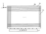
図1を参照しながら、本発明の第1の実施の形態による表示装置としての液晶表示装置10について説明する。図1は、液晶表示装置10の概略構成を示す図面である。[First Embodiment]
[Liquid Crystal Display]
A liquid
液晶表示装置10は、表示パネル2、ソースドライバ3、ゲートドライバ6、表示制御回路4及び電源5を備える。表示パネル2は、アクティブマトリクス基板20aと、対向基板20bと、これらの基板間に封入された液晶層(図示略)とを含む。
The liquid
アクティブマトリクス基板20aは、ソースドライバ3及びゲートドライバ6に対して、電気的に接続されている。ソースドライバ3及びゲートドライバ6は、例えば、フレキシブル基板に形成されている。ゲートドライバ6は、アクティブマトリクス基板20aに形成されていてもよい。表示制御回路4は、表示パネル2、ソースドライバ3、ゲートドライバ6及び電源5に対して、電気的に接続されている。表示制御回路4は、ソースドライバ3と、ゲートドライバ16とに対して、制御信号を出力する。制御信号には、例えば、リセット信号、クロック信号、データ信号等が含まれる。電源5は、表示パネル2、ソースドライバ3、ゲートドライバ6及び表示制御回路4に対して、電気的に接続されている。電源5は、表示パネル2、ソースドライバ3、ゲートドライバ6及び表示制御回路4に対して、電源電圧を供給する。
The
[アクティブマトリクス基板]
図2を参照しながら、アクティブマトリクス基板20aについて説明する。図2は、アクティブマトリクス基板20aの概略構成を示す模式図である。[Active matrix substrate]
The
アクティブマトリクス基板20aにおいては、複数のゲート線GLがY方向に略一定の間隔で形成されている。複数のゲート線GLは、ゲートドライバ6に接続されている。
In the
アクティブマトリクス基板20aにおいては、複数のデータ線としての複数のソース線SLがX方向に略一定の間隔で形成されている。複数のソース線SLは、複数のゲート線GLと交差する。複数のソース線SLは、ソースドライバ3に接続されている。
In the
Y方向で隣り合う2つのゲート線GLと、X方向で隣り合う2つのソース線SLとで囲まれる領域32が、1つの画素を形成している。対向基板20bが、例えば、赤(R)、緑(G)、青(B)の3色のカラーフィルタを含む場合、各画素は、カラーフィルタのいずれかの色に対応して配置される。つまり、表示パネル2は、複数の画素からなる表示領域30を有する。
A
領域32には、画素電極34が配置されている。つまり、アクティブマトリクス基板20aにおいては、複数の画素電極34がマトリクス状に配置されている。
A
領域32には、回路素子としての薄膜トランジスタ(以下、TFT−PIX)が配置されている。TFT−PIXにおいて、ゲートはゲート線GLに接続されている。ソースは、ソース線SLに接続されている。ドレインは、画素電極34に接続されている。
In the
液晶表示装置10においては、ゲートドライバ6により、複数のゲート線GLを順次走査する。ソースドライバ3により、各ソース線SLにデータ信号を供給する。これにより、表示パネル2に画像が表示される。
In the liquid
[静電気対策]
図2を参照しながら、アクティブマトリクス基板20aを保護する保護部50について説明する。図2に示す例では、複数(本実施形態では、2つ)の保護部50が配置されているが、保護部50は1つであってもよい。[Countermeasure against static electricity]
The
保護部50は、複数の保護回路50Aと、導電部50Bとを含む。
The
複数の保護回路50Aの各々は、ゲート線GLとソース線SLとの交点の近傍に配置されている。特に本実施形態では、複数の保護回路50Aの各々は、領域32に配置されている。つまり、複数の領域32の各々に、1つの保護回路50Aが配置されている。これら複数の領域32は、同じ列に配置されている。保護回路50Aの詳細については、後述する。
Each of the plurality of
導電部50Bは、保護配線52と、共通配線54と、保護回路56とを含む。
The
保護配線52は、導電性を有する材料からなる。保護配線52は、例えば、金属膜であってもよいし、透明導電膜であってもよい。保護配線52は、アクティブマトリクス基板20aに形成される。保護配線52は、例えば、ソース線SLと同じ層に形成される。保護配線52は、ソース線SLと平行に形成される。保護配線52は、複数の領域32に亘って形成される。つまり、保護配線52は、複数のゲート線GLと交差する。
The
共通配線54は、導電性を有する材料からなる。共通配線54は、例えば、金属膜であってもよいし、透明導電膜であってもよい。共通配線54は、アクティブマトリクス基板20aに形成される。共通配線54は、表示領域30の周辺に形成される。つまり、共通配線54は、額縁領域に形成される。共通配線54は、例えば、ゲート線GLと同じ層に形成される。共通配線54は、ゲート線GLと平行に形成される。
The
保護回路56は、保護配線52と、共通配線54とを接続する。図2に示す例では、保護回路56は、2つのダイオードを逆向きに並列接続したものであるが、保護回路56は、このような構成に限定されない。保護回路56は、表示領域の周辺に形成されている。つまり、保護回路56は、額縁領域に形成されている。
The
図3〜図6を参照しながら、保護回路50Aについて説明する。図3及び図4は、保護回路50Aの回路図である。図5は、保護回路50Aの概略構成を示す平面図である。図6は、保護回路50Aの概略構成を示す断面図である。
The
図3に示すように、保護回路50Aは、ダイオード58A及びダイオード58Bを含む。ダイオード58Bは、ダイオード58Aと並列に配置され、ダイオード58Aと逆向きに接続されている。
As shown in FIG. 3, the
図4に示す構成により、ダイオード58A及びダイオード58Bが実現される。保護回路50Aは、2つの薄膜トランジスタ(以下、TFT−P1及びTFT−P2とする)を含む。TFT−P1及びTFT−P2は、並列に配置される。
With the configuration shown in FIG. 4, the
TFT−P1では、ソースS1がゲートG1に接続されている。つまり、ゲートG1とソースS1が短絡している。要するに、ゲートG1とソースS1とがダイオード接続されている。これにより、ダイオード58Aが実現されている。ソースS1は、保護配線52に接続されている。ドレインD1は、ゲート線GLに接続されている。
In the TFT-P1, the source S1 is connected to the gate G1. That is, the gate G1 and the source S1 are short-circuited. In short, the gate G1 and the source S1 are diode-connected. Thereby, the
TFT−P2では、ソースS2がゲートG2に接続されている。つまり、ゲートG2とソースS2が短絡している。要するに、ゲートG2とソースS2とがダイオード接続されている。これにより、ダイオード58Bが実現されている。ソースS2は、ゲート線GLに接続されている。ドレインD2は、保護配線52に接続されている。
In TFT-P2, the source S2 is connected to the gate G2. That is, the gate G2 and the source S2 are short-circuited. In short, the gate G2 and the source S2 are diode-connected. Thereby, the
図5及び図6に示すように、ゲートG1及びゲートG2は、ベース基板60に接して形成されている。ベース基板60は、アクティブマトリクス基板20aに含まれる。ゲートG1及びゲートG2は、図5に示すように、ベース基板60の面内方向に離れて配置され、互いに平行である。ゲートG1及びゲートG2は、例えば、金属膜であってもよいし、透明導電膜であってもよい。
As shown in FIGS. 5 and 6, the gate G <b> 1 and the gate G <b> 2 are formed in contact with the
ゲートG1及びゲートG2は、絶縁層62で覆われている。絶縁層62は、例えば、シリコン酸化膜であってもよいし、シリコン窒化膜であってもよい。
The gate G1 and the gate G2 are covered with an insulating
絶縁層62に接して、半導体層64A及び半導体層64Bが形成されている。半導体層64A及び半導体層64Bは、例えば、アモルファスシリコンからなる。半導体層64A及び半導体層64Bは、チャネルを形成する。半導体層64A及び半導体層64Bは、図5に示すように、ベース基板60の面内方向に離れて配置され、互いに平行である。半導体層64Aは、平面視で、ゲートG1に重なる。半導体層64Bは、図5に示すように、平面視で、ゲートG2に重なる。
A
半導体層64A、64B及び絶縁層62に接して、ソースS1及びソースS2が形成されている。ソースS1及びソースS2は、例えば、金属膜であってもよいし、透明導電膜であってもよい。図5に示すように、ソースS1の一部がゲートG1に重なる。ソースS2の一部がゲートG2に重なる。絶縁層62には、ソースS1とゲートG1とが重なる領域において、コンタクトホールCH1が形成されている。絶縁層62には、ソースS2とゲートG2とが重なる領域において、コンタクトホールCH2が形成されている。コンタクトホールCH1を介して、ソースS1がゲートS1に接続されている。コンタクトホールCH2を介して、ソースS2がゲートS2に接続されている。ソースS1は、ドレインD2に接続されている。ドレインD2は、図5に示すように、平面視で、半導体層64A及び半導体層64Bに重なる。ソースS2は、ドレインD1に接続されている。ドレインD1は、図5に示すように、平面視で、半導体層64A及び半導体層64Bに重なる。
A source S1 and a source S2 are formed in contact with the semiconductor layers 64A and 64B and the insulating
ソースS1及びソースS2は、絶縁層66で覆われている。絶縁層66は、例えば、シリコン酸化膜であってもよいし、シリコン窒化膜であってもよい。
The source S1 and the source S2 are covered with an insulating
ゲートG1には、ゲート線GLが接続されている。ソースS2には、保護配線52が接続されている。
A gate line GL is connected to the gate G1. A
[保護部の動作]
保護部50は、例えば、アクティブマトリクス基板20aを製造するときに、アクティブマトリクス基板20aを静電気から保護する。具体的には、以下のとおりである。[Protection part operation]
For example, when the
静電気に起因して、ゲート線GLの電位がプラス方向に変化する場合を想定する。この場合、ゲートG2の電位が高くなる。これにより、TFT−P2がオンになる。その結果、ゲート線GLから保護配線52に電流が流れ、ゲート線GLの電位が低くなる。つまり、ゲート線GLの電位が所定の電位(例えば、変化する前の電位)に近づく。
Assume that the potential of the gate line GL changes in the positive direction due to static electricity. In this case, the potential of the gate G2 becomes high. Thereby, TFT-P2 is turned on. As a result, a current flows from the gate line GL to the
静電気に起因して、ゲート線GLの電位がマイナス方向に変化する場合を想定する。この場合、ゲートG1の電位が相対的に高くなる。これにより、TFT−P1がオンになる。その結果、ゲート線GLから保護配線52に電流が流れ、ゲート線GLの電位が低くなる。つまり、ゲート線GLの電位が所定の電位(例えば、変化する前の電位)に近づく。
Assume that the potential of the gate line GL changes in the negative direction due to static electricity. In this case, the potential of the gate G1 becomes relatively high. Thereby, TFT-P1 is turned on. As a result, a current flows from the gate line GL to the
なお、ゲートドライバ6によってゲート線GLが選択されていることを示す信号(ゲート選択信号)がゲート線GLを流れる場合には、ゲート線GLの電位は高くなるが、TFT−P2がオンになることはない。つまり、ゲート選択信号は、ゲート線GLだけに流れ、保護配線52及び共通配線54には流れない。
When a signal indicating that the gate line GL is selected by the gate driver 6 (gate selection signal) flows through the gate line GL, the potential of the gate line GL is increased, but the TFT-P2 is turned on. There is nothing. That is, the gate selection signal flows only to the gate line GL and does not flow to the
上述のようにして、静電気に起因する電流がゲート線GLから保護配線52に流れる。ゲート線GLから保護配線52に流れてきた電流(静電気に起因する電流)は、保護回路56を介して、共通配線54に流れる。
As described above, a current due to static electricity flows from the gate line GL to the
保護回路56は、図2に示すように、2つのダイオードを並列に配置し、且つ、逆向きに接続した構成を有する。保護回路56の構成として、例えば、図4に示す構成を採用することができる。この場合、保護回路56は、保護回路50Aと同じように動作する。
As shown in FIG. 2, the
ここで、ソース線SLは、図4に示すように、保護回路59を介して、共通配線54に接続されている。保護回路59は、図2に示すように、2つのダイオードを並列に配置し、且つ、逆向きに接続した構成を有する。保護回路59の構成として、例えば、図4に示す構成を採用することができる。この場合、保護回路59は、保護回路50Aと同じように動作する。静電気に起因して、ソース線SLの電位が変化した場合には、ゲート線GLの場合と同様に、静電気に起因する電流がソース線SLから共通配線54に流れる。これにより、全てのゲート線GLと全てのソース線SLとが同じ電位になる。その結果、静電気に起因して、例えば、ゲート線GLとソース線SLとの交点で放電したり、THT−PIXで放電したりするのを抑制できる、つまり、アクティブマトリクス基板20aを静電破壊から保護することができる。
Here, the source line SL is connected to the
液晶表示装置10においては、保護回路50Aが表示領域30内に配置されている。そのため、保護回路50Aが額縁領域に配置されている場合と比べて、額縁領域の幅を狭くすることができる。
In the liquid
[第1の実施の形態の応用例]
図2Aに示すように、ゲート線GLを、保護回路56を介して、共通配線54Gに接続し、且つ、ソース線SLを、保護回路59を介して、共通配線54Sに接続してもよい。共通配線54Gは、保護回路59Gを介して、共通電極61に接続してもよい。共通配線54Sは、保護回路59Sを介して、共通電極61に接続してもよい。[Application example of the first embodiment]
As shown in FIG. 2A, the gate line GL may be connected to the common wiring 54G via the
[保護回路の応用例1]
図7Aを参照しながら、表示領域30内に配置される保護回路の応用例1について説明する。応用例1に係る保護回路50A1は、保護回路50Aと比べて、TFT−P1が2つの薄膜トランジスタ(以下、TFT−P11及びTFT−P12とする)からなる。[Protection circuit application example 1]
Application example 1 of the protection circuit arranged in the
TFT−P11及びTFT−P12は、直列に接続されている。TFT−P11とTFT−P12との間には、導電体70が配置されている。TFT−P11のドレインD11は、導電体70に接続されている。TFT−P12のソースS11は、導電体70に接続されている。TFT−P11のソースS11は、保護配線52に接続されている。TFT−P12のドレインD12は、ゲート線GLに接続されている。TFT−P11のゲートG11は、保護配線52に接続されている。TFT−P12のゲートG12は、ゲート線GLに接続されている。
TFT-P11 and TFT-P12 are connected in series. A
応用例1に係る保護回路50A1は、保護回路50Aと比べて、TFT−P2のゲートG2が導電体70に接続されている。
In the protection circuit 50A1 according to the application example 1, the gate G2 of the TFT-P2 is connected to the
保護回路50A1の動作は、以下のとおりである。 The operation of the protection circuit 50A1 is as follows.
静電気に起因して、ゲート線GLの電位がプラス方向に変化する場合を想定する。この場合、ゲートG12の電位が高くなる。これにより、TFT−P12がオンになる。その結果、ゲートG2の電位が高くなる。 Assume that the potential of the gate line GL changes in the positive direction due to static electricity. In this case, the potential of the gate G12 increases. As a result, the TFT-P12 is turned on. As a result, the potential of the gate G2 increases.
このとき、ゲートG11は、保護配線52に接続されている。そのため、ゲートG11の電位は高くならない。その結果、ゲートG2の電位は、高い状態が維持される。
At this time, the gate G11 is connected to the
このようにして、ゲートG2の電位が高くなることで、TFT−P2がオンになる。その結果、ゲート線GLから保護配線52に電流が流れ、ゲート線GLの電位が低くなる。
In this way, the potential of the gate G2 is increased, so that the TFT-P2 is turned on. As a result, a current flows from the gate line GL to the
[保護回路の応用例2]
図7Bを参照しながら、表示領域30内に配置される保護回路の応用例2について説明する。応用例2に係る保護回路50A2は、保護回路50A1と比べて、ゲートG11及びゲートG12が電気的に孤立している。つまり、ゲートG11及びゲートG12は、何れの導電体にも接続されていない。[
Application example 2 of the protection circuit arranged in the
保護回路50A2の動作は、以下のとおりである。 The operation of the protection circuit 50A2 is as follows.
静電気に起因して、ゲート線GLの電位がプラス方向に変化する場合を想定する。この場合、寄生容量C1GS、C1GD、C2GS、C2GDにより、ゲートG11及びゲートG12の電位が高くなる。そのため、TFT−P11及びTFT−P12がオンになる。その結果、導電体70の電位が高くなる。このようにして、導電体70の電位が高くなることにより、TFT−P2がオンになる。その結果、ゲート線GLから保護配線52に電流が流れ、ゲート線GLの電位が低くなる。Assume that the potential of the gate line GL changes in the positive direction due to static electricity. In this case, the parasitic capacitance C1 GS, C1 GD, C2 GS , C2 GD, the potential of the gate G11 and the gate G12 becomes high. Therefore, TFT-P11 and TFT-P12 are turned on. As a result, the potential of the
[保護回路の応用例3]
図7Cを参照しながら、表示領域30内に配置される保護回路の応用例3について説明する。応用例3に係る保護回路50A3は、保護回路50A2と比べて、TFT−P2のゲートG2と、導電体70との間に、容量C1が配置されている。[
Application example 3 of the protection circuit arranged in the
保護回路50A3は、保護回路50A2と同様に動作する。ここで、保護回路50A3では、容量C1が配置されている。これにより、容量C1の充放電に要する時間だけ、TFT−P1がオンになっている状態を長くすることができる。 The protection circuit 50A3 operates in the same manner as the protection circuit 50A2. Here, in the protection circuit 50A3, the capacitor C1 is arranged. As a result, the state in which the TFT-P1 is on can be lengthened by the time required for charging and discharging the capacitor C1.
[保護回路の応用例4]
図7Dを参照しながら、表示領域30内に配置される保護回路の応用例4について説明する。応用例4に係る保護回路50A4は、ゲート線GLと保護配線52との間に配置される抵抗ERによって実現される。[
Application example 4 of the protection circuit arranged in the
図8A及び図8Bを参照しながら、抵抗ERについて説明する。ゲート線GLは、ベース基板60に接して形成されている。ゲート線GLは、例えば、金属膜である。ゲート線GLは、延出部74を含む。
The resistor ER will be described with reference to FIGS. 8A and 8B. The gate line GL is formed in contact with the
ゲート線GLは、絶縁層62で覆われている。絶縁層62に接して、保護配線52が形成されている。保護配線52は、例えば、金属膜である。保護配線52は、延出部72を含む。保護配線52は、絶縁層64で覆われている。
The gate line GL is covered with an insulating
絶縁層64に接して、接続配線76が形成されている。接続配線76は、例えば、透明導電膜である。図8Aに示すように、接続配線76は、延出部72及び延出部74に重なる。
A
絶縁層64には、接続配線76が延出部72に重なる領域、及び、接続配線76が延出部74に重なる領域において、コンタクトホールCH3、CH4が形成されている。コンタクトホールCH3を介して、接続配線76が延出部72に接続されている。コンタクトホールCH4を介して、接続配線76が延出部74に接続されている。
In the insulating layer 64, contact holes CH <b> 3 and CH <b> 4 are formed in a region where the
抵抗ERは、接続配線76と延出部72との接触抵抗、及び、接続配線76と延出部74との接触抵抗により、実現される。
The resistance ER is realized by the contact resistance between the
抵抗ERを大きくするために、例えば、接触配線76と延出部72との接触抵抗を大きくしてもよい。
In order to increase the resistance ER, for example, the contact resistance between the
図8Cを参照して、延出部72は、複数(本実施形態では、3つ)の延出部72A、72B、72Cからなる。延出部72Aは、保護配線52に接続されている。延出部72Bは、所定の隙間を介して、延出部72Aの隣に位置する。延出部72Cは、所定の隙間を介して、延出部72Bの隣に位置する。延出部72A、延出部72B及び延出部72Cは、同じ層に形成されている。
With reference to FIG. 8C, the extending
図8Cを参照して、接続配線76は、複数(本実施形態では、3つ)の接続配線76A、76B、76Cからなる。接続配線76Aは、延出部74及び延出部72Cに重なる。接続配線76Bは、所定の隙間を介して、接続配線76Aの隣に位置する。接続配線76Bは、延出部72C及び延出部72Bに重なる。接続配線76Cは、所定の隙間を介して、接続配線76Bの隣に位置する。接続配線76Cは、延出部72B及び延出部72Aに重なる。接続配線76A、接続配線76B及び接続配線76Cは、同じ層に形成されている。
Referring to FIG. 8C, the
絶縁層64には、接続配線76Aが延出部74に重なる領域、接続配線76Aが延出部72Cに重なる領域、接続配線76Bが延出部72Cに重なる領域、接続配線76Bが延出部72Bに重なる領域、接続配線76Aが延出部72Bに重なる領域、及び、接続配線76Aが延出部72Aに重なる領域に、コンタクトホールCH11〜CH16が形成されている。コンタクトホールCH11を介して、接続配線76Aが延出部74に接続されている。コンタクトホールCH12を介して、接続配線76Aが延出部72Cに接続されている。コンタクトホールCH13を介して、接続配線76Bが延出部72Cに接続されている。コンタクトホールCH14を介して、接続配線76Bが延出部72Bに接続されている。コンタクトホールCH15を介して、接続配線76Aが延出部72Bに接続されている。コンタクトホールCH16を介して、接続配線76Aが延出部72Aに接続されている。
In the insulating layer 64, the
図8Cに示す例では、抵抗ERは、接続配線76Aと延出部74との接触抵抗、接続配線76Aと延出部72Cとの接触抵抗、接続配線76Bと延出部72Cとの接触抵抗、接続配線76Bと延出部72Bとの接触抵抗、接続配線76Aと延出部72Bとの接触抵抗、及び、接続配線76Aと延出部72Aとの接触抵抗により、実現される。したがって、各接触抵抗の大きさを適当に設定することにより、図8Aに示す例よりも、抵抗ERを大きくすることができる。
In the example shown in FIG. 8C, the resistance ER is the contact resistance between the
[画素電極と保護配線との関係]
上述のように、保護配線52は、複数の領域32に亘って形成される。そのため、保護配線52を形成することによる画素の光透過率の低下を抑える必要がある。以下、液晶の動作モードごとに、画素電極34と保護配線52との関係を説明する。なお、以下に説明する画素電極34の形状は一例である。[Relationship between pixel electrode and protective wiring]
As described above, the
[MVAモード]
図9は、液晶の動作モードがMVA(Multi Domain Vertical Alignment)モードであ
る場合の画素電極34と保護配線52との関係の一例を示す。図9に示す例では、画素電極34は、複数のスリット34Aを有する。これにより、画素電極34は、複数の電極部34Bを有する。隣り合う2つの電極部34B、34Bは、連結部34Cによって連結されている。複数のスリット34Aの各々は、平面視において、対向基板20bに設けられた複数のリブ80とは異なる位置に形成されている。スリット34A及びリブ80は、液晶分子の配向の境界に位置する。そのため、スリット34A及びリブ80が形成された位置では、光の透過率が低い。つまり、スリット34A及びリブ80は、表示に寄与しない部分となる。[MVA mode]
FIG. 9 shows an example of the relationship between the
図9に示す例では、保護配線52は、スリット34Aが形成された位置に配置されている。上述のように、スリット34Aが形成された位置では、光の透過率が低い。そのため、保護配線52によって画素の光透過率が低下するのを抑制できる。
In the example shown in FIG. 9, the
図9に示す例では、保護配線52がスリット34の位置に形成されている場合と、保護配線52がスリット34の位置からずれた場合とで、画素の光透過率にばらつきが生じる。そこで、図9Aに示すように、保護配線52のX方向での端縁52Aを、電極部34BのX方向での端縁34B1と交差させる。これにより、保護配線52の位置がX方向にずれても、画素の光透過率がばらつき難くなる。なお、図9Aに示す例では、リブ80の図示は省略している。
In the example illustrated in FIG. 9, the light transmittance of the pixels varies between when the
[PVAモード]
図10は、液晶の動作モードがPVA(Patterned Vertical Alignment)モードである場合の画素電極34と保護配線52との関係の一例を示す。図10に示す例では、画素電極34は、複数のスリット34Aを有する。これにより、画素電極34は、複数の電極部34Bを有する。隣り合う2つの電極部34B、34Bは、連結部34Cによって連結されている。複数のスリット34Aの各々は、平面視において、対向基板20bに設けられた複数のスリット81とは異なる位置に形成されている。複数のスリット81は、対向基板20bに設けられた対向電極に形成されている。スリット34A及びスリット81は、液晶分子の配向の境界に位置する。そのため、スリット34A及びスリット81が形成された位置では、光の透過率が低い。つまり、スリット34A及びスリット81は、表示に寄与しない部分となる。[PVA mode]
FIG. 10 shows an example of the relationship between the
図10に示す例では、保護配線52は、スリット34Aが形成された位置に配置されている。上述のように、スリット34Aが形成された位置では、光の透過率が低い。そのため、保護配線52によって画素の光透過率が低下するのを抑制できる。
In the example illustrated in FIG. 10, the
なお、図10に示す例においても、図9Aに示す場合と同様に、保護配線52を配置してもよい。
In the example shown in FIG. 10 as well, the
[PSAモード]
図11は、液晶の動作モードがPSA(Polymer Sustained Alignment)モードである
場合の画素電極34と保護配線52との関係の一例を示す。図11に示す例では、画素電極34は、複数のスリット34Dを有する。これにより、画素電極34は、複数の電極部34Eと、電極部34Fと、電極部34Gとを有する。複数の電極部34Eの各々は、X方向及びY方向と交差する方向に延びる。電極部34Fは、X方向に延びる。電極部34Gは、Y方向に延びる。複数の電極部34Eの各々は、電極部34F又は電極部34Gの何れかに接続されている。電極部34Fは、電極部34Gに接続されている。電極部34Fは、電極部34Gと交差している。電極部34F及び電極部34Gは、液晶分子の配向の境界に位置する。そのため、電極部34F及び電極部34Gが形成された位置では、暗線が発生する。つまり、電極部34F及び電極部34Gは、表示に寄与しない部分となる。[PSA mode]
FIG. 11 shows an example of the relationship between the
図11に示す例では、保護配線52は、電極部34Gと重なる位置に配置されている。上述のように、電極部34Gが形成された位置では、暗線が発生する。そのため、保護配線52によって画素の光透過率が低下するのを抑制できる。
In the example shown in FIG. 11, the
図11に示す例では、保護配線52が電極部34Gの位置に形成されている場合と、保護配線52が電極部34Gの位置からずれた場合とで、画素の光透過率にばらつきが生じる。そこで、図11Aに示すように、保護配線52のX方向での端縁52Aを、電極部34DのX方向での端縁34B1と交差させる。これにより、保護配線52の位置がX方向にずれても、画素の光透過率がばらつき難くなる。
In the example shown in FIG. 11, the light transmittance of the pixels varies between when the
[UV2Aモード]
図12は、液晶の動作モードがUV2A(Ultra-violet induced multi-domain Vertical Alignment)モードである場合の画素電極34と保護配線52との関係の一例を示す。図12に示す例では、画素電極34と重なる位置に、暗線領域82、つまり、表示に寄与しない部分が形成される。その理由について、図12A〜図12Cを参照しながら説明する。[UV 2 A mode]
FIG. 12 shows an example of the relationship between the
図12Aは、アクティブマトリクス基板20a側の配向膜における配向方向であって、1画素内の配向方向を示す。図12Aに示す例では、1画素内の左半分と右半分とで配向方向が逆になっている。配向方向が異なることにより、液晶分子84にチルト角を与える方向が異なる。
FIG. 12A shows the alignment direction in the alignment film on the
図12Bは、対向基板20b側の配向膜における配向方向であって、1画素内の配向方向を示す。図12Bに示す例では、1画素内の上半分と下半分とで配向方向が逆になっている。配向方向が異なることにより、液晶分子84にチルト角を与える方向が異なる。対向基板20b側の配向膜の配向方向は、アクティブマトリクス基板20a側の配向膜の配向方向と直交している。
FIG. 12B shows the alignment direction in one alignment pixel in the alignment film on the
図12Cは、電圧が印加されたときの1画素内における液晶分子84の配向方向を示す。図12Cに示すように、領域A1、領域B1、領域C1及び領域D1では、液晶分子84の配向方向が異なる。そのため、暗線領域82が形成される。
FIG. 12C shows the alignment direction of the
図12に示す例では、保護配線52は、暗線領域82と重なる位置に配置されている。そのため、保護配線52によって画素の光透過率が低下するのを抑制できる。
In the example illustrated in FIG. 12, the
図12に示す例では、保護配線52が暗線領域82に重なる場合と、保護配線52が暗線領域82に重ならない場合とで、画素の光透過率にばらつきが生じる。そこで、図12Dに示すように、保護配線52が、暗線領域82と、暗線領域82以外の領域とに重なるようにする。つまり、保護配線52が、表示に寄与しない部分と、表示に寄与する部分とに重なるようにする。これにより、保護配線52の位置がX方向にずれても、画素の光透過率がばらつき難くなる。
In the example shown in FIG. 12, the light transmittance of the pixels varies depending on whether the
[IPSモード]
図13は、液晶の動作モードがIPS(In-Plane Switching)モードである場合の画素電極34と保護配線52との関係の一例を示す。図13に示す例では、画素電極34は、複数の電極部34Hと、連結部34Iとを備える。複数の電極部34Hは、Y方向に延び、且つ、X方向に並んで配置される。連結部34Iは、複数の電極部34Hの長さ方向一端を連結する。[IPS mode]
FIG. 13 shows an example of the relationship between the
共通電極86は、ゲート線GLと同じ層に形成されている。共通電極86は、複数の電極部86Aと、連結部86Bとを備える。複数の電極部86Aは、Y方向に延び、且つ、X方向に並んで配置される。複数の電極部86Aと複数の電極部34Hとは、平面視で交互に並んでいる。連結部86Bは、複数の電極部86Aの長さ方向の一端を連結する。
The
保護配線52は、複数の電極部86Aの1つと、保護回路50Aとを接続する。
The
図13に示す例では、保護配線52は、画素電極34及び共通電極86と重ならない位置に形成される。そのため、保護配線52によって画素の光透過率が低下するのを抑制できる。
In the example shown in FIG. 13, the
[FFSモード]
図14は、液晶の動作モードがFFS(Fringe Field Switching)モードである場合の画素電極34と保護配線52との関係の一例を示す。図14に示す例では、画素電極34は、複数の電極部34Jと、一対の連結部34K、34Kとを備える。複数の電極部34Jは、Y方向に延び、且つ、X方向に並んで配置される。一対の連結部34K、34Kは、X方向に延びる。一方の連結部34Kは、複数の電極部34Jの長さ方向の一端を連結する。他方の連結部34Kは、複数の電極部34Jの長さ方向の他端を連結する。画素電極34は、平面視で、共通電極88と重なる。保護配線52は、コンタクトホールCH21を介して、共通電極88に接続されている。[FFS mode]
FIG. 14 shows an example of the relationship between the
図14A及び図14Bを参照しながら、保護回路50Aと、保護配線52と、共通電極88との関係について説明する。図14に示す例では、保護回路50Aは、図5及び図6に示す構成を有する。したがって、保護回路50Aについての説明は省略する。なお、ドレインD2はソース保護配線52に接続されている。
The relationship among the
絶縁層66に接して、共通電極88が形成されている。共通電極88は、例えば、透明導電膜からなる。絶縁層66には、保護配線52が形成された位置において、コンタクトホールCH21が形成されている。コンタクトホールCH21を介して、保護配線52が共通電極88に接続されている。
A
共通電極88は、絶縁層90によって覆われている。絶縁層90は、例えば、シリコン酸化膜であってもよいし、シリコン窒化膜であってもよいし、有機樹脂膜であってもよい。絶縁層90に接して、画素電極34が形成されている。
The
図14に示す例では、保護配線52は、画素電極34と重ならない位置に形成される。そのため、保護配線52によって画素の光透過率が低下するのを抑制できる。
In the example shown in FIG. 14, the
図15は、液晶の動作モードがFFSモードである場合の画素電極34と保護配線52との関係の他の一例を示す。図15に示す例は、図14に示す例と比べて、保護配線52が画素電極34と交差する。例えば、後述する第2の実施の形態で説明するように、表示領域内にゲートドライバを配置する場合には、保護配線52として、画素の光透過率を調整するためのダミー配線を利用すればよい。
FIG. 15 shows another example of the relationship between the
図15Aは、液晶の動作モードがFFSモードである場合の画素電極34と保護配線52との関係の他の一例を示す。図15Aに示す例では、図15に示す例と比べて、保護配線52のX方向での端縁52Aを、電極部34JのX方向での端縁34J1と交差させる。これにより、保護配線52の位置がX方向にずれても、画素の光透過率がばらつき難くなる。
FIG. 15A shows another example of the relationship between the
[第2の実施の形態]
[液晶表示装置]
図16を参照しながら、本発明の第2の実施の形態による表示装置としての液晶表示装置1について説明する。図16は、液晶表示装置1の概略構成を示す図面である。[Second Embodiment]
[Liquid Crystal Display]
A liquid
液晶表示装置1は、表示パネル2、ソースドライバ3、表示制御回路4及び電源5を備える。表示パネル2は、アクティブマトリクス基板20aと、対向基板20bと、これらの基板間に封入された液晶層(図示略)とを含む。
The liquid
アクティブマトリクス基板20aは、ソースドライバ3に対して、電気的に接続されている。ソースドライバ3は、例えば、フレキシブル基板に形成されている。表示制御回路4は、表示パネル2、ソースドライバ3及び電源5に対して、電気的に接続されている。表示制御回路4は、ソースドライバ3と、ゲートドライバ11(図18参照)とに対して、制御信号を出力する。ゲートドライバ11は、アクティブマトリクス基板20aに形成されている。制御信号には、例えば、リセット信号(CLR)、クロック信号(CKA,CKB)、データ信号等が含まれる。電源5は、表示パネル2、ソースドライバ3及び表示制御回路4に対して、電気的に接続されている。電源5は、表示パネル2、ソースドライバ3及び表示制御回路4に対して、電源電圧(VSS)を供給する。
The
[アクティブマトリクス基板]
図17及び図18を参照しながら、アクティブマトリクス基板20aについて説明する。図17は、アクティブマトリクス基板20aの概略構成を示す図面である。図18は、ソース線SLの図示を省略したアクティブマトリクス基板20aと、アクティブマトリクス基板20aに接続されている各部の概略構成を示す図面である。[Active matrix substrate]
The
図17に示すように、アクティブマトリクス基板20aにおいては、複数(本実施形態では、n本)のゲート線GLがY方向に略一定の間隔で形成されている。アクティブマトリクス基板20aにおいては、複数のデータ線としての複数のソース線SLがX方向に略一定の間隔で形成されている。複数のソース線SLは、複数のゲート線GLと交差する。Y方向で隣り合う2つのゲート線GLと、X方向で隣り合う2つのソース線SLとで囲まれる領域が、1つの画素を形成している。対向基板20bが、例えば、赤(R)、緑(G)、青(B)の3色のカラーフィルタを含む場合、各画素は、カラーフィルタのいずれかの色に対応して配置される。つまり、複数のゲート線GL及び複数のソース線SLにより、表示領域が規定されている。
As shown in FIG. 17, in the
図18に示すように、ゲートドライバ11は、Y方向で隣り合う2つのゲート線GLの間に形成されている。各ゲート線GLに対して、4つのゲートドライバ11が接続されている。4つのゲートドライバ11は、略等間隔に配置されている。
As shown in FIG. 18, the
アクティブマトリクス基板20aの額縁領域には、端子部12gが形成されている。端子部12gは、制御回路4及び電源5と接続されている。端子部12gには、制御回路4から出力される制御信号や、電源5から出力される電源電圧が入力される。端子部12gに入力された制御信号及び電源電圧は、配線15Lを介して各ゲートドライバ11に供給される。
A
ゲートドライバ11は、供給される制御信号に応じて、接続されているゲート線GLに対し、状態信号を出力する。状態信号は、ゲートドライバ11に接続されているゲート線GLが選択された状態であるか否かを示す。また、ゲートドライバ11は、次段のゲート線GLに対し、上記状態信号を出力する。1つのゲート線GLに接続されている4つのゲートドライバ11の動作は、同期している。
The
アクティブマトリクス基板20aの額縁領域には、ソースドライバ3とソース線SLとを接続する端子部12sが形成されている。ソースドライバ3は、表示制御回路4から入力される制御信号に応じて、各ソース線SLにデータ信号を出力する。
In the frame region of the
[ゲートドライバの構成]
図19を参照しながら、ゲートドライバ11の構成について説明する。図19は、ゲート線GL(k)とゲート線GL(k−1)の間に配置され、ゲート線GL(k)に接続されているゲートドライバ11(以下、ゲートドライバ11(k)とする)の等価回路の一例を示す図である。ここで、kは、1〜nまでの任意の整数である。[Gate driver configuration]
The configuration of the
ゲートドライバ11は、複数のスイッチング素子として、アルファベットA〜Jで示す薄膜トランジスタ(以下、TFT−A〜TFT-J)を含む。ゲートドライバ11は、キャパシタCbstと、内部配線としてのnetA及びnetBをさらに含む。ここで、netAは、TFT-Aのドレインと、TFT−Bのドレインと、TFT−Cのドレインと、キャパシタCbstの一方の電極と、TFT−Fのゲートとを接続する。netBは、TFT−Cのゲートと、TFT−Gのドレインと、TFT−Hのドレインと、TFT−Iのドレインと、TFT−Jのドレインとを接続する。
The
TFT−Aにおいて、ゲートには、リセット信号CLRが入力される。ドレインには、netAが接続されている。ソースには、電源電圧VSSが入力される。 In the TFT-A, the reset signal CLR is input to the gate. NetA is connected to the drain. The power supply voltage VSS is input to the source.
TFT−Bにおいて、ゲート及びソースには、前段のゲート線GL(k−1)が接続されている。つまり、ゲート及びソースには、セット信号SSが入力される。なお、ゲート線GL(1)を駆動するゲートドライバ11のTFT−Bにおいては、セット信号SSとして、表示制御回路4から出力されるゲートスタートパルス信号が入力される。TFT−Bにおいて、ドレインには、netAが接続されている。
In the TFT-B, the previous gate line GL (k−1) is connected to the gate and the source. That is, the set signal SS is input to the gate and the source. Note that the gate start pulse signal output from the
TFT−Cにおいて、ゲートには、netBが接続されている。ドレインには、netAが接続されている。ソースには、電源電圧VSSが入力される。 In TFT-C, netB is connected to the gate. NetA is connected to the drain. The power supply voltage VSS is input to the source.
TFT−Dにおいて、ゲートには、クロック信号CKBが入力される。ドレインには、ゲート線GL(k)が接続されている。ソースには、電源電圧VSSが入力される。 In the TFT-D, the clock signal CKB is input to the gate. A gate line GL (k) is connected to the drain. The power supply voltage VSS is input to the source.
TFT−Eにおいて、ゲートには、リセット信号CLRが入力される。ドレインには、ゲート線GL(k)が接続されている。ソースには、電源電圧VSSが入力される。 In the TFT-E, a reset signal CLR is input to the gate. A gate line GL (k) is connected to the drain. The power supply voltage VSS is input to the source.
TFT−Fにおいて、ゲートには、netAが接続されている。ドレインには、ゲート線GL(k)が接続されている。ソースには、クロック信号CKAが入力される。 In the TFT-F, the netA is connected to the gate. A gate line GL (k) is connected to the drain. A clock signal CKA is input to the source.
TFT−Gにおいて、ゲート及びソースには、クロック信号CKBが入力される。ドレインには、netBが接続されている。 In the TFT-G, the clock signal CKB is input to the gate and the source. NetB is connected to the drain.
TFT−Hにおいて、ゲートには、クロック信号CKAが入力される。ドレインには、netBが接続されている。ソースには、電源電圧VSSが入力される。 In the TFT-H, the clock signal CKA is input to the gate. NetB is connected to the drain. The power supply voltage VSS is input to the source.
TFT−Iにおいて、ゲートには、リセット信号CLRが入力される。ドレインには、netBが接続されている。ソースには、電源電圧VSSが入力される。 In the TFT-I, the reset signal CLR is input to the gate. NetB is connected to the drain. The power supply voltage VSS is input to the source.
TFT−Jにおいて、ゲートには、前段のゲート線GL(k−1)が接続されている。つまり、ゲートには、セット信号Sが入力される。ドレインには、netBが接続されている。ソースには、電源電圧VSSが入力される。 In the TFT-J, the previous gate line GL (k−1) is connected to the gate. That is, the set signal S is input to the gate. NetB is connected to the drain. The power supply voltage VSS is input to the source.
ここで、TFT−Jは、TFT−Gよりも能力が大きく設定されている。具体的には、例えば、以下の(1)〜(3)の何れかである。
(1)TFT−Jのチャネル幅がTFT−Gのチャネル幅より大きい。
(2)TFT−Jのチャネル長がTFT−Gのチャネル長より短い。
(3)TFT−Jのチャネル幅がTFT−Gのチャネル幅より大きく、且つ、TFT−Jのチャネル長がTFT−Gのチャネル長より短い。Here, the capability of TFT-J is set larger than that of TFT-G. Specifically, for example, it is one of the following (1) to (3).
(1) The channel width of TFT-J is larger than the channel width of TFT-G.
(2) The channel length of TFT-J is shorter than the channel length of TFT-G.
(3) The channel width of TFT-J is larger than the channel width of TFT-G, and the channel length of TFT-J is shorter than the channel length of TFT-G.
キャパシタCbstにおいて、一方の電極は、netAと接続されている。他方の電極は、netBと接続されている。 In the capacitor Cbst, one electrode is connected to netA. The other electrode is connected to netB.
クロック信号CKAとクロック信号CKBは、一水平走査期間毎に位相が反転する2相のクロック信号である(図21参照)。図19は、ゲートドライバ11(k)を示しているが、後段のゲートドライバ11(k+1)及び前段のゲートドライバ11(k−1)では、TFT−Dのゲートに入力されるクロック信号は、クロック信号CKAである。TFT−Fのソースに入力されるクロック信号は、クロック信号CKBである。TFT−Gのゲートに入力されるクロック信号は、クロック信号CKAである。TFT−Hのゲートに入力されるクロック信号は、クロック信号CKBである。 The clock signal CKA and the clock signal CKB are two-phase clock signals whose phases are inverted every horizontal scanning period (see FIG. 21). FIG. 19 shows the gate driver 11 (k). In the rear gate driver 11 (k + 1) and the front gate driver 11 (k−1), the clock signal input to the gate of the TFT-D is This is the clock signal CKA. The clock signal input to the source of the TFT-F is the clock signal CKB. The clock signal input to the gate of the TFT-G is the clock signal CKA. The clock signal input to the gate of the TFT-H is the clock signal CKB.
[ゲートドライバの配置]
図20を参照しながら、表示領域内でのゲートドライバ11の配置について説明する。図20は、表示領域内でのゲートドライバ11の配置を示す模式図である。なお、図20におけるアルファベットA〜Jは、図4に示すTFT−A〜TFT−Jに対応している。[Gate driver layout]
The arrangement of the
隣り合う2つのゲート線GLの間には、ゲートドライバ11を構成する各素子が分散して配置されている。図20に示す例では、ゲートドライバ11(k−1)を構成する各素子と、ゲートドライバ11(k)を構成する各素子と、ゲートドライバ11(k+1)を構成する各素子と、ゲートドライバ11(k+2)を構成する各素子とは、同じ列の画素PIXに配置されている。ゲートドライバ11(k−1)を構成するTFT−A〜TFT−Jは、配線15Lを介して、ゲートドライバ11(k)を構成するTFT−A〜TFT−Jと、ゲートドライバ11(k+1)を構成するTFT−A〜TFT−Jと、ゲートドライバ11(k+2)を構成するTFT−A〜TFT−Jと接続されている。配線L、netA及びnetBは、例えば、層間コンタクトを介して、ソース線SLが形成された層と同じ層及びソース線SLが形成された層とは異なる層に形成される。これにより、配線L、netA及びnetBと、ソース線SLとの電気的な短絡が回避される。
The elements constituting the
[ゲートドライバの動作]
図19及び図21を参照しながら、ゲートドライバ11の動作について説明する。図21は、ゲートドライバ11(k)がゲート線GL(k)の電位を制御するときのタイミングチャートである。[Operation of gate driver]
The operation of the
ゲートドライバ11(k)には、表示制御回路4から供給され、一水平走査期間(1H)毎に位相が反転するクロック信号CKA、CKBが入力される。なお、図21では図示を省略しているが、ゲートドライバ11(k)には、表示制御回路4から供給され、一垂直走査期間毎に一定期間H(High)レベルとなるリセット信号CLRが入力される。リセット信号CLRが入力されることにより、netA、netB及びゲート線GL(k)の電位は、L(Low)レベルになる。
The gate driver 11 (k) is supplied with clock signals CKA and CKB that are supplied from the
図21の時刻t0からt1において、Lレベルのクロック信号CKAがTFT−Fのソース及びTFT−Hのゲートに入力される。また、Hレベルのクロック信号CKBがTFT−Dのゲート及びTFT−Gのゲート及びソースに入力される。これにより、TFT−Gがオンになり、TFT−Hがオフになる。その結果、netBの電位がHレベルになる。また、TFT−CとTFT−Dがオンになり、TFT−Fがオフになる。これにより、netAの電位がLレベルになる。その結果、ゲート線GL(k)の電位がLレベルになる。つまり、ゲート線GL(k)が非選択の状態となる。 From time t0 to t1 in FIG. 21, the L level clock signal CKA is input to the source of the TFT-F and the gate of the TFT-H. Further, an H level clock signal CKB is input to the gate of TFT-D and the gate and source of TFT-G. As a result, the TFT-G is turned on and the TFT-H is turned off. As a result, the potential of netB becomes H level. In addition, TFT-C and TFT-D are turned on, and TFT-F is turned off. As a result, the potential of netA becomes L level. As a result, the potential of the gate line GL (k) becomes L level. That is, the gate line GL (k) is not selected.
図21の時刻t1において、クロック信号CKAがHレベルとなり、クロック信号CKBがLレベルになる。これにより、TFT−Gがオフになり、TFT−Hがオンになる。その結果、netBの電位がLレベルになる。また、TFT−CとTFT−Dがオフになる。これにより、netAの電位がLレベルに維持される。その結果、ゲート線GL(k)の電位がLレベルに維持される。 At time t1 in FIG. 21, the clock signal CKA becomes H level and the clock signal CKB becomes L level. As a result, the TFT-G is turned off and the TFT-H is turned on. As a result, the potential of netB becomes L level. Also, TFT-C and TFT-D are turned off. As a result, the potential of netA is maintained at the L level. As a result, the potential of the gate line GL (k) is maintained at the L level.
図21の時刻t2において、クロック信号CKAがLレベル、クロック信号CKBがHレベルになる。これにより、ゲート線GL(k−1)を介して、セット信号SSが、TFT−Bのゲート及びソースと、TFT−Jのゲートとに、入力される。これにより、TFT−Bがオンになり、netAの電位がHレベルからTFT−Bの閾値電圧Vthを差し引いたレベルになる。また、TFT−J及びTFT−Gがオンになり、TFT−Hがオフになる。ここで、TFT−Jは、TFT−Gよりも能力が大きい。そのため、netBの電位がLレベルに維持される。また、TFT−C及びTFT−Fはオフになる。これにより、netAの電位が維持される。このとき、TFT−Dはオンになっている。これにより、ゲート線GL(k)の電位がLレベルに維持される。 At time t2 in FIG. 21, the clock signal CKA becomes L level and the clock signal CKB becomes H level. Thus, the set signal SS is input to the gate and source of the TFT-B and the gate of the TFT-J via the gate line GL (k−1). Thereby, the TFT-B is turned on, and the potential of the netA becomes a level obtained by subtracting the threshold voltage Vth of the TFT-B from the H level. In addition, TFT-J and TFT-G are turned on, and TFT-H is turned off. Here, the capability of TFT-J is greater than that of TFT-G. Therefore, the potential of netB is maintained at the L level. Also, TFT-C and TFT-F are turned off. Thereby, the potential of netA is maintained. At this time, the TFT-D is on. As a result, the potential of the gate line GL (k) is maintained at the L level.
図21の時刻t3において、クロック信号CKAがHレベルとなり、クロック信号CKBがLレベルとなる。これにより、TFT−Fがオンになり、TFT−Dがオフになる。netAとゲート線GL(k)との間には、キャパシタCbstが配置されている。そのため、TFT−Fのソースの電位が上昇するのに伴って、netAの電位はクロック信号CKAのHレベルよりも高くなる。このとき、TFT−G及びTFT−Jがオフになり、TFT−Hがオンになる。これにより、netBの電位がLレベルに維持される。また、TFT−Cはオフである。これにより、ゲート線GL(k)の電位がHレベルになる。つまり、ゲート線GL(k)が選択された状態となる。 At time t3 in FIG. 21, the clock signal CKA becomes H level and the clock signal CKB becomes L level. As a result, the TFT-F is turned on and the TFT-D is turned off. A capacitor Cbst is disposed between the netA and the gate line GL (k). Therefore, as the potential of the TFT-F source increases, the potential of netA becomes higher than the H level of the clock signal CKA. At this time, TFT-G and TFT-J are turned off, and TFT-H is turned on. As a result, the potential of netB is maintained at the L level. Also, TFT-C is off. As a result, the potential of the gate line GL (k) becomes H level. That is, the gate line GL (k) is selected.
図21の時刻t4において、クロック信号CKAがLレベルとなり、クロック信号CKBがHレベルになる。これにより、TFT−Gがオンになり、TFT−Hがオフになる。その結果、netBの電位がHレベルになる。netBの電位がHレベルになることにより、TFT−Cがオンになり、netAの電位がLレベルになる。このとき、TFT−Dがオンになり、TFT−Fがオフになる。これにより、ゲート線GL(k)の電位がLレベルになる。つまり、ゲート線GL(k)が選択されていない状態となる。 At time t4 in FIG. 21, the clock signal CKA becomes L level and the clock signal CKB becomes H level. As a result, the TFT-G is turned on and the TFT-H is turned off. As a result, the potential of netB becomes H level. When the potential of netB becomes H level, the TFT-C is turned on, and the potential of netA becomes L level. At this time, TFT-D is turned on and TFT-F is turned off. As a result, the potential of the gate line GL (k) becomes L level. That is, the gate line GL (k) is not selected.
このようにして、ゲートドライバ11(k)からセット信号SSがゲート線GL(k)に出力されることにより、ゲート線GL(k)が選択された状態となる。液晶表示装置1は、各ゲート線GLに接続されている複数のゲートドライバ11によって複数のゲート線GLを順次走査し、ソースドライバ3によって各ソース線SLにデータ信号を供給することにより表示パネル2に画像を表示する。
In this way, the set signal SS is output from the gate driver 11 (k) to the gate line GL (k), so that the gate line GL (k) is selected. The liquid
[静電気対策]
図22を参照しながら、アクティブマトリクス基板20aを静電気から保護するための保護部51について説明する。図22に示す例では、複数(本実施形態では、2つ)の保護部51が配置されているが、保護部51は1つであってもよい。[Countermeasure against static electricity]
A
保護部51は、保護部50と比べて、複数の保護回路51Aをさらに備える。複数の保護回路51Aの各々は、内部配線ILと保護配線52との交点の近くに配置される。内部配線ILは、例えば、netAやnetBである。保護回路51Aは、例えば、保護回路50Aと同じ構成を有する。
The
本実施形態では、静電気に起因して内部配線ILの電位がプラスの方向又はマイナスの方向に大きく変化した場合、静電気に起因してゲート線GLの電位がプラスの方向又はマイナスの方向に大きく変化した場合と同様に、保護回路51Aにより、内部配線ILの電位を所定の電位(例えば、変化する前の電位)にすることができる。
In the present embodiment, when the potential of the internal wiring IL greatly changes in the plus direction or the minus direction due to static electricity, the potential of the gate line GL greatly changes in the plus direction or minus direction due to the static electricity. Similarly to the case, the
本実施形態では、ゲートドライバ11が表示領域内に配置されている。そのため、表示領域外にゲートドライバ11が配置されている場合と比べて、額縁領域をより狭くすることができる。
In the present embodiment, the
[パネルの形状]
本実施形態では、ゲートドライバ11が表示領域内に配置される。そのため、例えば、図23や図24に示す形状の表示パネル2を実現できる。図23及び図24に示す領域92は、ゲートドライバ11が配置される領域である。[Panel shape]
In the present embodiment, the
保護配線52は、パネル2の形状に応じて、適当に配置される。
The
例えば、図23に示すように、パネル2が半円形状である場合には、領域92のX方向の中央に1つの保護配線52を配置すれば、全てのゲート線GLを静電気から保護することができる。
For example, as shown in FIG. 23, when the
例えば、図24に示すように、パネル2の縁が波形である場合には、全てのゲート線GLの電位を制御するために、複数の領域92を設ける必要がある。例えば、図24Aに示す例では、領域92A内のゲートドライバ11は、正常に動作しない状態、又は、正常に動作しない可能性が高い状態にある。領域92B内のゲートドライバ11は、正常に動作する。この場合、ゲート線GL1は、図24Aに示す領域92以外の領域92(具体的には、図24Aに示す領域92よりも左側に位置する領域92)内のゲートドライバ11によって、電位が制御される。ゲート線GL2〜GL4は、図24Aに示す領域92内のゲートドライバ11によって、電位が制御される。
For example, as shown in FIG. 24, when the edge of the
保護配線52は、例えば、領域92のX方向の両端に配置される。図24Aに示す例では、領域92の左端に位置する保護配線52により、つまり、領域92の左右両端に位置する保護配線52のうち、長いほうの保護配線52により、領域92内の全てのゲート線GLを保護することができる。
For example, the
以上、本発明の実施の形態を説明したが、上述した実施の形態は本発明を実施するための例示に過ぎない。よって、本発明は上述した実施の形態に限定されることなく、その趣旨を逸脱しない範囲内で上述した実施の形態を適宜変形、又は組み合わせて実施することが可能である。 While the embodiments of the present invention have been described above, the above-described embodiments are merely examples for carrying out the present invention. Therefore, the present invention is not limited to the above-described embodiment, and the above-described embodiment can be appropriately modified or combined without departing from the spirit of the present invention.
Claims (12)
前記表示領域内に形成され、前記複数の第1配線と交差する複数の第2配線とを備えるアクティブマトリクス基板であって、
前記表示領域内で前記複数の第1配線の各々に接続された複数の第1保護回路と、
前記表示領域内で前記複数の第1保護回路の各々に接続された保護配線とを含み、
前記複数の第1保護回路の各々は、
当該第1保護回路が接続された第1配線の電位に応じて、当該第1配線と前記保護配線との間での通電を許容する、アクティブマトリクス基板。 A plurality of first wirings formed in the display area;
An active matrix substrate including a plurality of second wirings formed in the display region and intersecting with the plurality of first wirings ;
A plurality of first protection circuit connected to each of the plurality of first wirings in front Symbol display area,
A protective wiring connected to each of the plurality of first protection circuits in the display area,
Each of the plurality of first protection circuits includes:
An active matrix substrate that allows energization between the first wiring and the protective wiring in accordance with the potential of the first wiring to which the first protection circuit is connected.
前記表示領域の周辺で前記保護配線に接続された第2保護回路と、
前記第2保護回路に接続された共通配線とを含む、アクティブマトリクス基板。 The active matrix substrate according to claim 1 ,
A second protection circuit connected to the protection lines around the front Symbol display area,
An active matrix substrate including a common wiring connected to the second protection circuit.
前記表示領域の周辺で前記複数の第2配線の各々に接続され、且つ、前記共通配線に接続された複数の第3保護回路を含む、アクティブマトリクス基板。 The active matrix substrate according to claim 2 ,
An active matrix substrate including a plurality of third protection circuits connected to each of the plurality of second wirings around the display area and connected to the common wiring .
前記表示領域内で前記保護配線に接続され、前記複数の第1保護回路とは異なる複数の第4保護回路と、
前記複数の第4保護回路の各々に接続された複数の第3配線部とを含む、アクティブマトリクス基板。 The active matrix substrate according to claim 1 ,
Is connected to the protection lines before Symbol display region, a plurality of fourth protection circuit that is different from the plurality of first protection circuit,
An active matrix substrate including a plurality of third wiring portions connected to each of the plurality of fourth protection circuits.
前記共通配線は、前記第2保護回路が接続された第1共通配線と、前記第3保護回路が接続された第2共通配線とからなる、アクティブマトリクス基板。 The common wiring is an active matrix substrate including a first common wiring to which the second protection circuit is connected and a second common wiring to which the third protection circuit is connected.
前記第1共通配線は、第5保護回路を介して共通電極に接続され、 The first common wiring is connected to a common electrode through a fifth protection circuit,
前記第2共通配線は、第6保護回路を介して前記共通電極に接続された、アクティブマトリクス基板。 The second common wiring is an active matrix substrate connected to the common electrode through a sixth protection circuit.
前記複数の第1配線は、複数のゲート線を含み、
前記アクティブマトリクス基板は、さらに、
前記複数のゲート線に接続され、前記複数のゲート線の電位を制御する駆動部を備え、
前記駆動部は、
前記表示領域内に配置され、前記複数のゲート線の各々に少なくとも1つ接続される複数のゲートドライバを含む、アクティブマトリクス基板。 The active matrix substrate according to claim 1 ,
The plurality of first wirings includes a plurality of gate lines,
The active matrix substrate further includes:
A drive unit connected to the plurality of gate lines and controlling the potentials of the plurality of gate lines;
The drive unit is
An active matrix substrate including a plurality of gate drivers disposed in the display region and connected to at least one of the plurality of gate lines.
前記複数の第1配線は、さらに、
前記複数のゲートドライバの各々に少なくとも1つ設けられる複数の内部配線を含み、
前記複数の第1保護回路は、前記複数のゲート線の各々に接続され、
前記保護部は、さらに、
前記表示領域内で、前記複数の内部配線の各々に接続され、且つ、前記保護配線に接続され、前記複数の第1保護回路とは異なる複数の第4保護回路を含む、アクティブマトリクス基板。 The active matrix substrate according to claim 7 ,
Before SL plurality of first wiring further
A plurality of internal wirings provided at least one for each of the plurality of gate drivers;
A plurality of first protection circuits connected to each of the plurality of gate lines;
The protection unit further includes:
An active matrix substrate including a plurality of fourth protection circuits connected to each of the plurality of internal wirings and connected to the protection wirings and different from the plurality of first protection circuits in the display region.
前記第1保護回路は、
第1ダイオードと、
前記第1ダイオードと並列に配置され、前記第1ダイオードと逆向きに接続された第2ダイオードとを含む、アクティブマトリクス基板。 The active matrix substrate according to claim 1 ,
The first protection circuit includes:
A first diode;
An active matrix substrate, comprising: a second diode disposed in parallel with the first diode and connected in the opposite direction to the first diode.
前記第1保護回路は、
第1薄膜トランジスタと、
前記第1薄膜トランジスタと並列に配置された第2薄膜トランジスタとを含み、
前記第1薄膜トランジスタのソース及びドレインの一方をゲートに接続することにより、前記第1ダイオードが形成され、
前記第2薄膜トランジスタのソース及びドレインの一方をゲートに接続することにより、前記第2ダイオードが形成される、アクティブマトリクス基板。 The active matrix substrate according to claim 9 , wherein
The first protection circuit includes:
A first thin film transistor;
A second thin film transistor disposed in parallel with the first thin film transistor;
The first diode is formed by connecting one of a source and a drain of the first thin film transistor to a gate,
An active matrix substrate, wherein the second diode is formed by connecting one of a source and a drain of the second thin film transistor to a gate.
前記表示領域内に配置される複数の画素電極をさらに備え、
前記複数の画素電極の各々は、
表示に寄与しない部分を含み、
前記保護配線は、
前記表示に寄与しない部分に重なる部分を含む、アクティブマトリクス基板。 The active matrix substrate according to any one of claims 1 to 10 ,
A plurality of pixel electrodes disposed in the display area;
Each of the plurality of pixel electrodes is
Including parts that do not contribute to the display,
The protective wiring is
An active matrix substrate including a portion overlapping a portion that does not contribute to the display.
Applications Claiming Priority (3)
| Application Number | Priority Date | Filing Date | Title |
|---|---|---|---|
| JP2014094073 | 2014-04-30 | ||
| JP2014094073 | 2014-04-30 | ||
| PCT/JP2015/062770 WO2015166937A1 (en) | 2014-04-30 | 2015-04-28 | Active matrix substrate and display device comprising active matrix substrate |
Publications (2)
| Publication Number | Publication Date |
|---|---|
| JP6022118B2 true JP6022118B2 (en) | 2016-11-09 |
| JPWO2015166937A1 JPWO2015166937A1 (en) | 2017-04-20 |
Family
ID=54358664
Family Applications (1)
| Application Number | Title | Priority Date | Filing Date |
|---|---|---|---|
| JP2016516382A Active JP6022118B2 (en) | 2014-04-30 | 2015-04-28 | Active matrix substrate and display device including the active matrix substrate |
Country Status (4)
| Country | Link |
|---|---|
| US (1) | US9939696B2 (en) |
| JP (1) | JP6022118B2 (en) |
| CN (1) | CN106662783B (en) |
| WO (1) | WO2015166937A1 (en) |
Families Citing this family (13)
| Publication number | Priority date | Publication date | Assignee | Title |
|---|---|---|---|---|
| CN205384420U (en) * | 2016-01-07 | 2016-07-13 | 合肥鑫晟光电科技有限公司 | Display substrate and display device |
| CN105739206B (en) * | 2016-02-18 | 2018-12-21 | 深圳市华星光电技术有限公司 | array substrate and liquid crystal display device |
| CN205450520U (en) * | 2016-04-06 | 2016-08-10 | 京东方科技集团股份有限公司 | Array substrate and display device |
| US10147718B2 (en) * | 2016-11-04 | 2018-12-04 | Dpix, Llc | Electrostatic discharge (ESD) protection for the metal oxide medical device products |
| JP7021867B2 (en) * | 2017-05-30 | 2022-02-17 | 株式会社村上開明堂 | Mirror display device |
| JP6662831B2 (en) * | 2017-09-28 | 2020-03-11 | シャープ株式会社 | Active matrix substrate and X-ray imaging panel having the same |
| JP6753885B2 (en) * | 2018-04-16 | 2020-09-09 | シャープ株式会社 | How to fix defects in active matrix boards, display devices, and active matrix boards |
| US10852591B2 (en) * | 2018-06-29 | 2020-12-01 | Sharp Kabushiki Kaisha | Image display device |
| CN208622722U (en) * | 2018-08-30 | 2019-03-19 | 京东方科技集团股份有限公司 | Electrostatic discharge protection circuit and display device |
| US11366366B2 (en) * | 2019-02-13 | 2022-06-21 | Sharp Kabushiki Kaisha | Active matrix substrate and photoelectric imaging panel with the same |
| CN109979371A (en) * | 2019-04-15 | 2019-07-05 | 武汉华星光电技术有限公司 | A kind of display panel and device |
| CN111768700B (en) * | 2020-06-22 | 2021-10-08 | 武汉华星光电半导体显示技术有限公司 | Display panel and display device |
| CN118136639B (en) * | 2024-05-10 | 2024-08-02 | 惠科股份有限公司 | Array substrate and display panel |
Citations (5)
| Publication number | Priority date | Publication date | Assignee | Title |
|---|---|---|---|---|
| JPH07230098A (en) * | 1994-02-18 | 1995-08-29 | Sanyo Electric Co Ltd | Liquid crystal display device |
| JPH09146111A (en) * | 1995-11-28 | 1997-06-06 | Toshiba Corp | Array substrate for display device and its production and liquid crystal display device |
| JPH09265110A (en) * | 1996-03-28 | 1997-10-07 | Toshiba Corp | Active matrix panel |
| JP2007041096A (en) * | 2005-08-01 | 2007-02-15 | Sanyo Epson Imaging Devices Corp | Electrooptical device, its manufacturing method, and electronic equipment |
| JP2007310338A (en) * | 2006-05-18 | 2007-11-29 | Genta Kagi Kogyo Kofun Yugenkoshi | Active matrix device |
Family Cites Families (18)
| Publication number | Priority date | Publication date | Assignee | Title |
|---|---|---|---|---|
| JPS6179259A (en) | 1984-09-26 | 1986-04-22 | Seiko Instr & Electronics Ltd | thin film transistor device |
| JPH0830823B2 (en) | 1986-07-02 | 1996-03-27 | 株式会社日立製作所 | Liquid crystal display |
| JP2715936B2 (en) | 1994-09-30 | 1998-02-18 | 日本電気株式会社 | Thin film transistor type liquid crystal display device and manufacturing method thereof |
| KR100252308B1 (en) | 1997-01-10 | 2000-04-15 | 구본준, 론 위라하디락사 | Thin film transistor array |
| TW457690B (en) | 1999-08-31 | 2001-10-01 | Fujitsu Ltd | Liquid crystal display |
| KR100628254B1 (en) * | 2000-04-12 | 2006-09-27 | 엘지.필립스 엘시디 주식회사 | Liquid crystal display |
| KR100386849B1 (en) * | 2001-07-10 | 2003-06-09 | 엘지.필립스 엘시디 주식회사 | Circuit for electro static dischrging of tft-lcd |
| JP3714243B2 (en) * | 2001-12-11 | 2005-11-09 | セイコーエプソン株式会社 | Semiconductor device, electro-optical device, and electronic apparatus |
| TWI247168B (en) * | 2004-02-27 | 2006-01-11 | Au Optronics Corp | Liquid crystal display and ESD protection circuit thereon |
| JP4951841B2 (en) * | 2004-03-25 | 2012-06-13 | セイコーエプソン株式会社 | LCD panel |
| US7532265B2 (en) * | 2005-06-08 | 2009-05-12 | Wintek Corporation | Integrated circuit with the cell test function for the electrostatic discharge protection |
| JP4305486B2 (en) * | 2006-09-28 | 2009-07-29 | エプソンイメージングデバイス株式会社 | LCD panel |
| KR101657957B1 (en) | 2008-09-12 | 2016-09-20 | 가부시키가이샤 한도오따이 에네루기 켄큐쇼 | Display device |
| JP2011158690A (en) | 2010-02-01 | 2011-08-18 | Sony Corp | Liquid crystal display panel and electronic apparatus |
| CN104396017B (en) * | 2012-04-17 | 2018-08-24 | 东芝电子管器件株式会社 | Manufacture the method and X-ray flat-panel detector tft array substrate of X-ray flat-panel detector |
| TWI478139B (en) * | 2012-09-13 | 2015-03-21 | Au Optronics Corp | Electrostatic discharge protection circuit and display apparauts usning the same |
| JP6148734B2 (en) * | 2013-09-26 | 2017-06-14 | シャープ株式会社 | Display panel and display device including the same |
| US9772532B2 (en) * | 2014-03-10 | 2017-09-26 | Lg Display Co., Ltd. | Electrostatic discharge circuit and liquid crystal display device including the same |
-
2015
- 2015-04-28 JP JP2016516382A patent/JP6022118B2/en active Active
- 2015-04-28 CN CN201580023599.3A patent/CN106662783B/en not_active Expired - Fee Related
- 2015-04-28 US US15/305,394 patent/US9939696B2/en active Active
- 2015-04-28 WO PCT/JP2015/062770 patent/WO2015166937A1/en active Application Filing
Patent Citations (5)
| Publication number | Priority date | Publication date | Assignee | Title |
|---|---|---|---|---|
| JPH07230098A (en) * | 1994-02-18 | 1995-08-29 | Sanyo Electric Co Ltd | Liquid crystal display device |
| JPH09146111A (en) * | 1995-11-28 | 1997-06-06 | Toshiba Corp | Array substrate for display device and its production and liquid crystal display device |
| JPH09265110A (en) * | 1996-03-28 | 1997-10-07 | Toshiba Corp | Active matrix panel |
| JP2007041096A (en) * | 2005-08-01 | 2007-02-15 | Sanyo Epson Imaging Devices Corp | Electrooptical device, its manufacturing method, and electronic equipment |
| JP2007310338A (en) * | 2006-05-18 | 2007-11-29 | Genta Kagi Kogyo Kofun Yugenkoshi | Active matrix device |
Also Published As
| Publication number | Publication date |
|---|---|
| CN106662783A (en) | 2017-05-10 |
| US9939696B2 (en) | 2018-04-10 |
| WO2015166937A1 (en) | 2015-11-05 |
| US20170038650A1 (en) | 2017-02-09 |
| CN106662783B (en) | 2018-11-13 |
| JPWO2015166937A1 (en) | 2017-04-20 |
Similar Documents
| Publication | Publication Date | Title |
|---|---|---|
| JP6022118B2 (en) | Active matrix substrate and display device including the active matrix substrate | |
| JP6215490B2 (en) | Active matrix substrate and display panel | |
| JP6230074B2 (en) | Active matrix substrate and method of manufacturing active matrix substrate | |
| KR102485374B1 (en) | Display Device | |
| US10115369B2 (en) | Active matrix substrate, and display device including the active matrix substrate | |
| CN100422806C (en) | Liquid crystal display device | |
| US10078239B2 (en) | Sensor-equipped display device | |
| CN108196725B (en) | Touch display substrate and touch display device | |
| US9817276B2 (en) | Liquid crystal display device | |
| KR102444037B1 (en) | In-cell touch type display device and driving IC thereof | |
| TWI437335B (en) | Display device | |
| US20150301415A1 (en) | Liquid crystal display device | |
| US10627688B2 (en) | Active matrix substrate and display panel | |
| US9459482B2 (en) | Liquid crystal display device with touch panel | |
| US20160299614A1 (en) | Display panel, driving method thereof and display device | |
| CN105404064A (en) | Display device | |
| KR20170039001A (en) | In-cell touch type display device | |
| US20150338692A1 (en) | Display device | |
| TWI342460B (en) | Thin film transistor and liquid crystal display device | |
| KR20150106304A (en) | Electrostatic Discharge Circuit And Liquid Crystal Display Device Comprising The Same | |
| JP2003043523A (en) | Thin film transistor panel | |
| KR20080020331A (en) | Thin film transistor array panel | |
| KR102494157B1 (en) | Display Device |
Legal Events
| Date | Code | Title | Description |
|---|---|---|---|
| TRDD | Decision of grant or rejection written | ||
| A975 | Report on accelerated examination |
Free format text: JAPANESE INTERMEDIATE CODE: A971005 Effective date: 20160907 |
|
| A01 | Written decision to grant a patent or to grant a registration (utility model) |
Free format text: JAPANESE INTERMEDIATE CODE: A01 Effective date: 20160913 |
|
| A61 | First payment of annual fees (during grant procedure) |
Free format text: JAPANESE INTERMEDIATE CODE: A61 Effective date: 20161004 |
|
| R150 | Certificate of patent or registration of utility model |
Ref document number: 6022118 Country of ref document: JP Free format text: JAPANESE INTERMEDIATE CODE: R150 |