JP5935394B2 - 横電界方式の液晶表示装置 - Google Patents
横電界方式の液晶表示装置 Download PDFInfo
- Publication number
- JP5935394B2 JP5935394B2 JP2012045911A JP2012045911A JP5935394B2 JP 5935394 B2 JP5935394 B2 JP 5935394B2 JP 2012045911 A JP2012045911 A JP 2012045911A JP 2012045911 A JP2012045911 A JP 2012045911A JP 5935394 B2 JP5935394 B2 JP 5935394B2
- Authority
- JP
- Japan
- Prior art keywords
- liquid crystal
- optical compensation
- substrate
- compensation layer
- region
- Prior art date
- Legal status (The legal status is an assumption and is not a legal conclusion. Google has not performed a legal analysis and makes no representation as to the accuracy of the status listed.)
- Active
Links
- 239000004973 liquid crystal related substance Substances 0.000 title claims description 293
- 230000005684 electric field Effects 0.000 title claims description 81
- 239000000758 substrate Substances 0.000 claims description 177
- 230000003287 optical effect Effects 0.000 claims description 167
- 238000010521 absorption reaction Methods 0.000 claims description 75
- 238000000411 transmission spectrum Methods 0.000 claims description 5
- 230000010287 polarization Effects 0.000 description 60
- 238000000034 method Methods 0.000 description 27
- 238000002834 transmittance Methods 0.000 description 27
- 230000000007 visual effect Effects 0.000 description 23
- 239000010408 film Substances 0.000 description 21
- 239000011651 chromium Substances 0.000 description 12
- 229910052751 metal Inorganic materials 0.000 description 11
- 239000002184 metal Substances 0.000 description 11
- 229910021417 amorphous silicon Inorganic materials 0.000 description 10
- 230000000694 effects Effects 0.000 description 10
- 229920002284 Cellulose triacetate Polymers 0.000 description 8
- NNLVGZFZQQXQNW-ADJNRHBOSA-N [(2r,3r,4s,5r,6s)-4,5-diacetyloxy-3-[(2s,3r,4s,5r,6r)-3,4,5-triacetyloxy-6-(acetyloxymethyl)oxan-2-yl]oxy-6-[(2r,3r,4s,5r,6s)-4,5,6-triacetyloxy-2-(acetyloxymethyl)oxan-3-yl]oxyoxan-2-yl]methyl acetate Chemical compound O([C@@H]1O[C@@H]([C@H]([C@H](OC(C)=O)[C@H]1OC(C)=O)O[C@H]1[C@@H]([C@@H](OC(C)=O)[C@H](OC(C)=O)[C@@H](COC(C)=O)O1)OC(C)=O)COC(=O)C)[C@@H]1[C@@H](COC(C)=O)O[C@@H](OC(C)=O)[C@H](OC(C)=O)[C@H]1OC(C)=O NNLVGZFZQQXQNW-ADJNRHBOSA-N 0.000 description 8
- 230000005540 biological transmission Effects 0.000 description 8
- 229910052804 chromium Inorganic materials 0.000 description 8
- 238000005516 engineering process Methods 0.000 description 8
- 239000010409 thin film Substances 0.000 description 8
- 238000010586 diagram Methods 0.000 description 7
- 239000011159 matrix material Substances 0.000 description 7
- 239000004065 semiconductor Substances 0.000 description 7
- 229910052581 Si3N4 Inorganic materials 0.000 description 6
- HQVNEWCFYHHQES-UHFFFAOYSA-N silicon nitride Chemical compound N12[Si]34N5[Si]62N3[Si]51N64 HQVNEWCFYHHQES-UHFFFAOYSA-N 0.000 description 6
- VYZAMTAEIAYCRO-UHFFFAOYSA-N Chromium Chemical compound [Cr] VYZAMTAEIAYCRO-UHFFFAOYSA-N 0.000 description 5
- 229910004205 SiNX Inorganic materials 0.000 description 4
- 230000002349 favourable effect Effects 0.000 description 4
- 230000001681 protective effect Effects 0.000 description 4
- 150000001844 chromium Chemical class 0.000 description 3
- 210000002858 crystal cell Anatomy 0.000 description 3
- 238000009826 distribution Methods 0.000 description 3
- 239000011521 glass Substances 0.000 description 3
- 238000000059 patterning Methods 0.000 description 2
- 239000004988 Nematic liquid crystal Substances 0.000 description 1
- 230000005856 abnormality Effects 0.000 description 1
- 230000002411 adverse Effects 0.000 description 1
- 210000004027 cell Anatomy 0.000 description 1
- 238000006243 chemical reaction Methods 0.000 description 1
- 239000003086 colorant Substances 0.000 description 1
- 238000004040 coloring Methods 0.000 description 1
- 230000006866 deterioration Effects 0.000 description 1
- AMGQUBHHOARCQH-UHFFFAOYSA-N indium;oxotin Chemical compound [In].[Sn]=O AMGQUBHHOARCQH-UHFFFAOYSA-N 0.000 description 1
- 230000001678 irradiating effect Effects 0.000 description 1
- 239000000463 material Substances 0.000 description 1
- 230000002093 peripheral effect Effects 0.000 description 1
- 230000000704 physical effect Effects 0.000 description 1
- 239000011347 resin Substances 0.000 description 1
- 229920005989 resin Polymers 0.000 description 1
- 239000003566 sealing material Substances 0.000 description 1
- 238000004088 simulation Methods 0.000 description 1
- 125000006850 spacer group Chemical group 0.000 description 1
Images


Classifications
-
- G—PHYSICS
- G02—OPTICS
- G02F—OPTICAL DEVICES OR ARRANGEMENTS FOR THE CONTROL OF LIGHT BY MODIFICATION OF THE OPTICAL PROPERTIES OF THE MEDIA OF THE ELEMENTS INVOLVED THEREIN; NON-LINEAR OPTICS; FREQUENCY-CHANGING OF LIGHT; OPTICAL LOGIC ELEMENTS; OPTICAL ANALOGUE/DIGITAL CONVERTERS
- G02F1/00—Devices or arrangements for the control of the intensity, colour, phase, polarisation or direction of light arriving from an independent light source, e.g. switching, gating or modulating; Non-linear optics
- G02F1/01—Devices or arrangements for the control of the intensity, colour, phase, polarisation or direction of light arriving from an independent light source, e.g. switching, gating or modulating; Non-linear optics for the control of the intensity, phase, polarisation or colour
- G02F1/13—Devices or arrangements for the control of the intensity, colour, phase, polarisation or direction of light arriving from an independent light source, e.g. switching, gating or modulating; Non-linear optics for the control of the intensity, phase, polarisation or colour based on liquid crystals, e.g. single liquid crystal display cells
- G02F1/133—Constructional arrangements; Operation of liquid crystal cells; Circuit arrangements
- G02F1/13306—Circuit arrangements or driving methods for the control of single liquid crystal cells
-
- G—PHYSICS
- G02—OPTICS
- G02F—OPTICAL DEVICES OR ARRANGEMENTS FOR THE CONTROL OF LIGHT BY MODIFICATION OF THE OPTICAL PROPERTIES OF THE MEDIA OF THE ELEMENTS INVOLVED THEREIN; NON-LINEAR OPTICS; FREQUENCY-CHANGING OF LIGHT; OPTICAL LOGIC ELEMENTS; OPTICAL ANALOGUE/DIGITAL CONVERTERS
- G02F1/00—Devices or arrangements for the control of the intensity, colour, phase, polarisation or direction of light arriving from an independent light source, e.g. switching, gating or modulating; Non-linear optics
- G02F1/01—Devices or arrangements for the control of the intensity, colour, phase, polarisation or direction of light arriving from an independent light source, e.g. switching, gating or modulating; Non-linear optics for the control of the intensity, phase, polarisation or colour
- G02F1/13—Devices or arrangements for the control of the intensity, colour, phase, polarisation or direction of light arriving from an independent light source, e.g. switching, gating or modulating; Non-linear optics for the control of the intensity, phase, polarisation or colour based on liquid crystals, e.g. single liquid crystal display cells
- G02F1/133—Constructional arrangements; Operation of liquid crystal cells; Circuit arrangements
- G02F1/1333—Constructional arrangements; Manufacturing methods
- G02F1/1335—Structural association of cells with optical devices, e.g. polarisers or reflectors
- G02F1/13363—Birefringent elements, e.g. for optical compensation
- G02F1/133634—Birefringent elements, e.g. for optical compensation the refractive index Nz perpendicular to the element surface being different from in-plane refractive indices Nx and Ny, e.g. biaxial or with normal optical axis
-
- G—PHYSICS
- G02—OPTICS
- G02F—OPTICAL DEVICES OR ARRANGEMENTS FOR THE CONTROL OF LIGHT BY MODIFICATION OF THE OPTICAL PROPERTIES OF THE MEDIA OF THE ELEMENTS INVOLVED THEREIN; NON-LINEAR OPTICS; FREQUENCY-CHANGING OF LIGHT; OPTICAL LOGIC ELEMENTS; OPTICAL ANALOGUE/DIGITAL CONVERTERS
- G02F1/00—Devices or arrangements for the control of the intensity, colour, phase, polarisation or direction of light arriving from an independent light source, e.g. switching, gating or modulating; Non-linear optics
- G02F1/01—Devices or arrangements for the control of the intensity, colour, phase, polarisation or direction of light arriving from an independent light source, e.g. switching, gating or modulating; Non-linear optics for the control of the intensity, phase, polarisation or colour
- G02F1/13—Devices or arrangements for the control of the intensity, colour, phase, polarisation or direction of light arriving from an independent light source, e.g. switching, gating or modulating; Non-linear optics for the control of the intensity, phase, polarisation or colour based on liquid crystals, e.g. single liquid crystal display cells
- G02F1/133—Constructional arrangements; Operation of liquid crystal cells; Circuit arrangements
- G02F1/1333—Constructional arrangements; Manufacturing methods
- G02F1/1337—Surface-induced orientation of the liquid crystal molecules, e.g. by alignment layers
- G02F1/133753—Surface-induced orientation of the liquid crystal molecules, e.g. by alignment layers with different alignment orientations or pretilt angles on a same surface, e.g. for grey scale or improved viewing angle
-
- G—PHYSICS
- G02—OPTICS
- G02F—OPTICAL DEVICES OR ARRANGEMENTS FOR THE CONTROL OF LIGHT BY MODIFICATION OF THE OPTICAL PROPERTIES OF THE MEDIA OF THE ELEMENTS INVOLVED THEREIN; NON-LINEAR OPTICS; FREQUENCY-CHANGING OF LIGHT; OPTICAL LOGIC ELEMENTS; OPTICAL ANALOGUE/DIGITAL CONVERTERS
- G02F1/00—Devices or arrangements for the control of the intensity, colour, phase, polarisation or direction of light arriving from an independent light source, e.g. switching, gating or modulating; Non-linear optics
- G02F1/01—Devices or arrangements for the control of the intensity, colour, phase, polarisation or direction of light arriving from an independent light source, e.g. switching, gating or modulating; Non-linear optics for the control of the intensity, phase, polarisation or colour
- G02F1/13—Devices or arrangements for the control of the intensity, colour, phase, polarisation or direction of light arriving from an independent light source, e.g. switching, gating or modulating; Non-linear optics for the control of the intensity, phase, polarisation or colour based on liquid crystals, e.g. single liquid crystal display cells
- G02F1/133—Constructional arrangements; Operation of liquid crystal cells; Circuit arrangements
- G02F1/1333—Constructional arrangements; Manufacturing methods
- G02F1/1343—Electrodes
- G02F1/134309—Electrodes characterised by their geometrical arrangement
- G02F1/134363—Electrodes characterised by their geometrical arrangement for applying an electric field parallel to the substrate, i.e. in-plane switching [IPS]
-
- G—PHYSICS
- G02—OPTICS
- G02F—OPTICAL DEVICES OR ARRANGEMENTS FOR THE CONTROL OF LIGHT BY MODIFICATION OF THE OPTICAL PROPERTIES OF THE MEDIA OF THE ELEMENTS INVOLVED THEREIN; NON-LINEAR OPTICS; FREQUENCY-CHANGING OF LIGHT; OPTICAL LOGIC ELEMENTS; OPTICAL ANALOGUE/DIGITAL CONVERTERS
- G02F1/00—Devices or arrangements for the control of the intensity, colour, phase, polarisation or direction of light arriving from an independent light source, e.g. switching, gating or modulating; Non-linear optics
- G02F1/01—Devices or arrangements for the control of the intensity, colour, phase, polarisation or direction of light arriving from an independent light source, e.g. switching, gating or modulating; Non-linear optics for the control of the intensity, phase, polarisation or colour
- G02F1/13—Devices or arrangements for the control of the intensity, colour, phase, polarisation or direction of light arriving from an independent light source, e.g. switching, gating or modulating; Non-linear optics for the control of the intensity, phase, polarisation or colour based on liquid crystals, e.g. single liquid crystal display cells
- G02F1/137—Devices or arrangements for the control of the intensity, colour, phase, polarisation or direction of light arriving from an independent light source, e.g. switching, gating or modulating; Non-linear optics for the control of the intensity, phase, polarisation or colour based on liquid crystals, e.g. single liquid crystal display cells characterised by the electro-optical or magneto-optical effect, e.g. field-induced phase transition, orientation effect, guest-host interaction or dynamic scattering
-
- G—PHYSICS
- G02—OPTICS
- G02F—OPTICAL DEVICES OR ARRANGEMENTS FOR THE CONTROL OF LIGHT BY MODIFICATION OF THE OPTICAL PROPERTIES OF THE MEDIA OF THE ELEMENTS INVOLVED THEREIN; NON-LINEAR OPTICS; FREQUENCY-CHANGING OF LIGHT; OPTICAL LOGIC ELEMENTS; OPTICAL ANALOGUE/DIGITAL CONVERTERS
- G02F1/00—Devices or arrangements for the control of the intensity, colour, phase, polarisation or direction of light arriving from an independent light source, e.g. switching, gating or modulating; Non-linear optics
- G02F1/01—Devices or arrangements for the control of the intensity, colour, phase, polarisation or direction of light arriving from an independent light source, e.g. switching, gating or modulating; Non-linear optics for the control of the intensity, phase, polarisation or colour
- G02F1/13—Devices or arrangements for the control of the intensity, colour, phase, polarisation or direction of light arriving from an independent light source, e.g. switching, gating or modulating; Non-linear optics for the control of the intensity, phase, polarisation or colour based on liquid crystals, e.g. single liquid crystal display cells
- G02F1/133—Constructional arrangements; Operation of liquid crystal cells; Circuit arrangements
- G02F1/1333—Constructional arrangements; Manufacturing methods
- G02F1/1335—Structural association of cells with optical devices, e.g. polarisers or reflectors
- G02F1/13363—Birefringent elements, e.g. for optical compensation
- G02F1/133631—Birefringent elements, e.g. for optical compensation with a spatial distribution of the retardation value
-
- G—PHYSICS
- G02—OPTICS
- G02F—OPTICAL DEVICES OR ARRANGEMENTS FOR THE CONTROL OF LIGHT BY MODIFICATION OF THE OPTICAL PROPERTIES OF THE MEDIA OF THE ELEMENTS INVOLVED THEREIN; NON-LINEAR OPTICS; FREQUENCY-CHANGING OF LIGHT; OPTICAL LOGIC ELEMENTS; OPTICAL ANALOGUE/DIGITAL CONVERTERS
- G02F1/00—Devices or arrangements for the control of the intensity, colour, phase, polarisation or direction of light arriving from an independent light source, e.g. switching, gating or modulating; Non-linear optics
- G02F1/01—Devices or arrangements for the control of the intensity, colour, phase, polarisation or direction of light arriving from an independent light source, e.g. switching, gating or modulating; Non-linear optics for the control of the intensity, phase, polarisation or colour
- G02F1/13—Devices or arrangements for the control of the intensity, colour, phase, polarisation or direction of light arriving from an independent light source, e.g. switching, gating or modulating; Non-linear optics for the control of the intensity, phase, polarisation or colour based on liquid crystals, e.g. single liquid crystal display cells
- G02F1/133—Constructional arrangements; Operation of liquid crystal cells; Circuit arrangements
- G02F1/1333—Constructional arrangements; Manufacturing methods
- G02F1/1335—Structural association of cells with optical devices, e.g. polarisers or reflectors
- G02F1/13363—Birefringent elements, e.g. for optical compensation
- G02F1/133633—Birefringent elements, e.g. for optical compensation using mesogenic materials
-
- G—PHYSICS
- G02—OPTICS
- G02F—OPTICAL DEVICES OR ARRANGEMENTS FOR THE CONTROL OF LIGHT BY MODIFICATION OF THE OPTICAL PROPERTIES OF THE MEDIA OF THE ELEMENTS INVOLVED THEREIN; NON-LINEAR OPTICS; FREQUENCY-CHANGING OF LIGHT; OPTICAL LOGIC ELEMENTS; OPTICAL ANALOGUE/DIGITAL CONVERTERS
- G02F1/00—Devices or arrangements for the control of the intensity, colour, phase, polarisation or direction of light arriving from an independent light source, e.g. switching, gating or modulating; Non-linear optics
- G02F1/01—Devices or arrangements for the control of the intensity, colour, phase, polarisation or direction of light arriving from an independent light source, e.g. switching, gating or modulating; Non-linear optics for the control of the intensity, phase, polarisation or colour
- G02F1/13—Devices or arrangements for the control of the intensity, colour, phase, polarisation or direction of light arriving from an independent light source, e.g. switching, gating or modulating; Non-linear optics for the control of the intensity, phase, polarisation or colour based on liquid crystals, e.g. single liquid crystal display cells
- G02F1/133—Constructional arrangements; Operation of liquid crystal cells; Circuit arrangements
- G02F1/1333—Constructional arrangements; Manufacturing methods
- G02F1/1337—Surface-induced orientation of the liquid crystal molecules, e.g. by alignment layers
- G02F1/133753—Surface-induced orientation of the liquid crystal molecules, e.g. by alignment layers with different alignment orientations or pretilt angles on a same surface, e.g. for grey scale or improved viewing angle
- G02F1/133757—Surface-induced orientation of the liquid crystal molecules, e.g. by alignment layers with different alignment orientations or pretilt angles on a same surface, e.g. for grey scale or improved viewing angle with different alignment orientations
-
- G—PHYSICS
- G02—OPTICS
- G02F—OPTICAL DEVICES OR ARRANGEMENTS FOR THE CONTROL OF LIGHT BY MODIFICATION OF THE OPTICAL PROPERTIES OF THE MEDIA OF THE ELEMENTS INVOLVED THEREIN; NON-LINEAR OPTICS; FREQUENCY-CHANGING OF LIGHT; OPTICAL LOGIC ELEMENTS; OPTICAL ANALOGUE/DIGITAL CONVERTERS
- G02F2413/00—Indexing scheme related to G02F1/13363, i.e. to birefringent elements, e.g. for optical compensation, characterised by the number, position, orientation or value of the compensation plates
- G02F2413/03—Number of plates being 3
-
- G—PHYSICS
- G02—OPTICS
- G02F—OPTICAL DEVICES OR ARRANGEMENTS FOR THE CONTROL OF LIGHT BY MODIFICATION OF THE OPTICAL PROPERTIES OF THE MEDIA OF THE ELEMENTS INVOLVED THEREIN; NON-LINEAR OPTICS; FREQUENCY-CHANGING OF LIGHT; OPTICAL LOGIC ELEMENTS; OPTICAL ANALOGUE/DIGITAL CONVERTERS
- G02F2413/00—Indexing scheme related to G02F1/13363, i.e. to birefringent elements, e.g. for optical compensation, characterised by the number, position, orientation or value of the compensation plates
- G02F2413/07—All plates on one side of the LC cell
-
- G—PHYSICS
- G02—OPTICS
- G02F—OPTICAL DEVICES OR ARRANGEMENTS FOR THE CONTROL OF LIGHT BY MODIFICATION OF THE OPTICAL PROPERTIES OF THE MEDIA OF THE ELEMENTS INVOLVED THEREIN; NON-LINEAR OPTICS; FREQUENCY-CHANGING OF LIGHT; OPTICAL LOGIC ELEMENTS; OPTICAL ANALOGUE/DIGITAL CONVERTERS
- G02F2413/00—Indexing scheme related to G02F1/13363, i.e. to birefringent elements, e.g. for optical compensation, characterised by the number, position, orientation or value of the compensation plates
- G02F2413/08—Indexing scheme related to G02F1/13363, i.e. to birefringent elements, e.g. for optical compensation, characterised by the number, position, orientation or value of the compensation plates with a particular optical axis orientation
Landscapes
- Physics & Mathematics (AREA)
- Nonlinear Science (AREA)
- Chemical & Material Sciences (AREA)
- Crystallography & Structural Chemistry (AREA)
- General Physics & Mathematics (AREA)
- Optics & Photonics (AREA)
- Mathematical Physics (AREA)
- Geometry (AREA)
- Spectroscopy & Molecular Physics (AREA)
- Liquid Crystal (AREA)
Description
二枚の互いに平行な透明絶縁性の基板と、
これらの基板の間に挟持され、前記基板に略平行な方向に配向され前記基板に略平行な横電界が印加される液晶を有する液晶層と、
前記液晶の初期配向方向が互いに直交する領域I及び領域IIと、
前記二枚の基板のそれぞれの外側に一枚ずつ配置され、前記領域I及び領域IIのいずれかの前記初期配向方向に一致しかつ互いに直交する吸収軸を有する二枚の偏光板と、
前記基板の少なくとも一方と前記液晶層との間に配置され、前記液晶の初期配向方向と同一の方向に一軸光学異方性を有する第1の光学補償層と、
前記基板の一方とこの基板側に配置された前記偏光板との間に配置され、当該偏光板の吸収軸に平行な方向に一軸光学異方性を有する第2の光学補償層と、
前記第2の光学補償層と直近の前記偏光板との間に配置され、前記基板に垂直な方向に一軸光学異方性を有する第3の光学補償層と、
を備え、
前記第1の光学補償層が正の一軸屈折率異方性を有し、
当該第1の光学補償層の有するリターデーションと前記液晶層の有するリターデーションとの和が500〜600[nm]の間にある、
ものである。
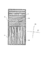
本発明の実施形態1について、図1、図2、図3、図4、図5を用いて説明する。すなわち、ここでの説明で用いる符号は、図1乃至図5のいずれかに開示されている。図1は、実施形態1に係る液晶表示装置における1画素の光学的な機能を果たす主要要素の構成(一部の図示を省略している。)を示す。図2は1画素の平面図である。図3は、図2のA−A’の断面図を示す。図4は、画素内の表示領域における初期配向方向の分割を示したものである。図5は分割に伴う構成を断面図で模式化したものである。
p’=p×s
a’=a×s
n1’=n1×s
n2’=n2×s
ap’=ap×s
cp’=cp×s
となる。
本発明の実施形態2について、図8を用いて説明する。実施形態1では、図5に示すように、出射側偏光板23と基板21との間に、基板21側から外側Aプレート24とCプレート25を配置することにより、斜め視野からの光漏れを抑制する。このような外側Aプレート24とCプレート25とを重ねた位相補償は、この部分を図8に示すように、第4の光学補償層としての二軸の光学補償層である二軸補償層32で置き換えた場合でも、同等の効果を得ることができる。二軸補償層32と偏光板23との間には、支持基板となるTAC層33が配置されている。
本発明の実施形態3について、図10を用いて説明する。実施形態1では、図5に示すように、出射側偏光板23と基板21との間には、基板21側からこの順に外側Aプレート24とCプレート25を配置することにより、斜め視野からの光漏れを抑制する。本実施形態3では、外側第2の光学補償層としてのAプレート24と第3の光学補償層としてのCプレート25とを、入射側偏光板22と基板20との間に配置する。
本発明の実施形態4について、図11を用いて説明する。実施形態3では、図10に示すように、入射側偏光板22と基板20との間に、入射側偏光板22側からCプレート25と外側Aプレート24を配置することにより、斜め視野からの光漏れを抑制する。このような外側Aプレート24とCプレート25とを重ねた位相補償は、この部分を図11に示すように、二軸補償層32で置き換えた場合でも、同等の効果を得ることができる。
本発明の実施形態5について、図12を用いて説明する。本実施形態5では、実施形態1と同様に、出射側偏光板23と基板21との間に、基板21側から外側Aプレート24とCプレート25を配置する。ただし、本実施形態5では、第1の光学補償層としてのインセルリターダー10r,10g,10bのリターデーション量を、それぞれRGB3色のカラーフィルタの色層18r、18g、18bに対応するサブ画素ごとに変える。
本発明の実施形態6について、図15及び図16を用いて説明する。図15は1画素の平面図である。図16は、1画素内の表示領域における初期配向方向の分割を示したものである。図15及び図16に示すように、本実施形態6では、実施形態1と比べて、領域I及び領域IIにおけるストライプ状の画素電極5の延在方向及び液晶の初期配向方向29,31のみを変えている。画素の上半分の領域IIでは、水平方向(走査線3の延在方向)にストライプ電極を延在させ、画素の下半分の領域Iでは、これと直交させる方向にストライプ電極を延在させてある。
本発明の実施形態7について、図17、図18及び図19を用いて説明する。すなわち、ここでの説明で用いる符号は、図17乃至図19のいずれかに開示されている。図17は1画素の平面図である。図18は、図17のA−A’の断面図を示す。図19は、1画素内の表示領域における初期配向方向の分割を示す。
本実施形態8では、画素の構成及び光学要素の配置を実施形態1と同様にして、図20に示すように、透明絶縁性基板21と液晶層12aとの間に配置する第1の光学補償層としてのインセルリターダー58を、負の屈折率異方性を有するものとする。インセルリターダー58の異方軸の方向は、液晶12の初期配向方向に一致させる。インセルリターダー58のリターデーションの大きさは、液晶層12aのリターデーションに対して絶対値を等しく符号を反対とする。これにより、両者のリターデーションの合計を約0[nm]とする。
本実施形態9では、画素の構成及び光学要素の配置は、実施形態2と同様にして、図22に示すように、透明絶縁性基板21と液晶層12aとの間に配置するインセルリターダー58を負の屈折率異方性を有するものとする。
次に、本発明の実施形態の効果について詳しく説明する。本発明の実施形態により、初期配向状態で液晶配向を直交させた二領域を有する横電界方式の液晶表示装置において、黒表示時に斜め視野から見た場合にも良好な表示が得られる視野角の広い良好な横電界方式の液晶表示装置が得られた。
p’=p×s
a’=a×s
n1’=n1×s
n2’=n2×s
ap’=ap×s
cp’=cp×s
となる。
これらの基板の間に挟持され、前記基板に略平行な方向に配向され前記基板に略平行な横電界が印加される液晶を有する液晶層と、
前記液晶の初期配向方向が互いに直交する領域I及び領域IIと、
前記二枚の基板のそれぞれの外側に一枚ずつ配置され、前記領域I及び領域IIのいずれかの前記初期配向方向に一致しかつ互いに直交する吸収軸を有する二枚の偏光板と、
前記基板の少なくとも一方と前記液晶層との間に配置され、前記液晶の初期配向方向と同一の方向に一軸光学異方性を有する第1の光学補償層と、
前記基板の一方とこの基板側に配置された前記偏光板との間に配置され、当該偏光板の吸収軸に平行な方向に一軸光学異方性を有する第2の光学補償層と、
前記第2の光学補償層と直近の前記偏光板との間に配置され、前記基板に垂直な方向に一軸光学異方性を有する第3の光学補償層と、
を備えた横電界方式の液晶表示装置。
これらの基板の間に挟持され、前記基板に略平行な方向に配向され前記基板に略平行な電界が印加される液晶を有する液晶層と、
前記液晶の初期配向方向が互いに直交する領域I及び領域IIと、
前記二枚の基板のそれぞれの外側に一枚ずつ配置され、前記領域I及び領域IIのいずれかの前記初期配向方向に一致しかつ互いに直交する吸収軸を有する二枚の偏光板と、
前記基板の少なくとも一方と前記液晶層との間に配置され、前記液晶の初期配向方向と同一の方向に一軸光学異方性を有する第1の光学補償層と、
前記基板の一方とこの基板側に配置された前記偏光板との間に配置され、二軸性の光学異方性を有する第4の光学補償層と、を備え、
前記第4の光学補償層の主軸は、前記基板に平行な面内で前記偏光板の吸収軸と平行な方向及びこれに垂直な方向、並びに前記基板に垂直な方向である、
横電界方式の液晶表示装置。
付記1又は2記載の横電界方式の液晶表示装置。
前記サブ画素において、前記第1の光学補償層の有するリターデーションと前記液晶層の有するリターデーションとの和が、当該サブ画素の有する前記カラーフィルタの透過率スペクトルのピークの90%以上のところから選択された波長に等しい、
付記1又は2記載の横電界方式の液晶表示装置。
付記1又は2記載の横電界方式の液晶表示装置。
付記1乃至5のいずれか一つに記載の横電界方式の液晶表示装置。
前記液晶の初期配向方向が直交する二領域を有し、
互いに直交した吸収軸を有する二枚の偏光板が前記二枚の基板のそれぞれの外側に一枚ずつ配置されており、
前記液晶の初期配向方向は、前記吸収軸のいずれかに一致しており、
前記二領域のそれぞれで、前記液晶の初期配向方向と同一の方向に一軸光学異方性を有する第1の光学補償層が、少なくとも一方の前記基板と前記液晶層との間に配置されており、
一方の前記基板とこの基板側に配置される前記偏光板との間には、当該偏光板の吸収軸に平行な方向に一軸光学異方性を有する第2の光学補償層が配置されており、
更にこの第2の光学補償層と当該偏光板との間に、前記基板に垂直な方向に一軸光学異方性を有する第3の光学補償層を有している、
ことを特徴とする横電界方式の液晶表示装置。
前記液晶の初期配向方向が直交する二領域を有し、
互いに直交した吸収軸を有する二枚の偏光板が前記二枚の基板のそれぞれの外側に一枚ずつ配置されており、
前記液晶の初期配向方向は、前記吸収軸のいずれかに一致しており、
前記二領域のそれぞれで、前記液晶の初期配向方向と同一の方向に一軸光学異方性を有する第1の光学補償層が、少なくとも一方の前記基板と前記液晶層との間に配置されており、
一方の前記基板とこの基板側に配置される前記偏光板の間には、二軸性の光学異方性を有する第4の光学補償層が配置されており、
前記第4の光学補償層の主軸は、前記基板に平行な面内で前記偏光板の吸収軸と平行な方向及びこれに垂直な方向、並びに前記基板に垂直な方向である、
ことを特徴とする横電界方式の液晶表示装置。
前記第1の光学補償層が正の一軸屈折率異方性を有し、
前記第1の光学補償層の有するリターデーションと前記液晶層の有するリターデーションとの和が500〜600[nm]の間にある、
ことを特徴とする横電界方式の液晶表示装置。
前記液晶表示装置の画素が2色以上のカラーフィルタを有するサブ画素からなり、
前記サブ画素において、前記第1の光学補償層の有するリターデーションと前記液晶層の有するリターデーションとの和が、前記各カラーフィルタの透過率スペクトルのピークの90%以上のところから選択された波長に等しい、
ことを特徴とする横電界方式の液晶表示装置。
前記第1の光学補償層が負の一軸屈折率異方性を有し、
前記第1の光学補償層の有するリターデーションと前記液晶層の有するリターデーションとの和が−50〜50[nm]の間にある、
ことを特徴とする横電界方式の液晶表示装置。
前記二領域を領域I、領域IIとしたとき、
前記領域Iで発生する前記横電界の方位と前記領域IIで発生する前記横電界の方位とは互いに直交しており、
前記領域Iにおける前記液晶の方位と前記横電界の方位とのなす角と、前記領域IIにおける前記液晶の方位と前記横電界の方位とのなす角とが、略同一である、
ことを特徴とする横電界方式の液晶表示装置。
1 平面状の共通電極
2 共通信号配線
3 走査線
4 データ線
5 ストライプ状の画素電極
6 薄膜半導体層
7s ソース電極
7d ドレイン電極
8 画素電極スルーホール
9 両端部(ストライプ状の画素電極を接続する部分)
10,10r,10g,10b インセルリターダー
11 インセルリターダー用配向膜
12 液晶
12a 液晶層
13 ゲート絶縁膜
14 保護絶縁膜
15、16 配向膜
17 ブラックマトリクス
18,18r、18g、18b 色層
19 オーバーコート層
20,21 透明絶縁性基板
22 入射側偏光板
23 出射側偏光板
24 Aプレート
25 Cプレート
26 入射側偏光板吸収軸
27 出射側偏光板吸収軸
28 TFTアレイ基板
29 領域Iの初期配向方向
30 カラーフィルタ基板
31 領域IIの初期配向方向
32 二軸補償層
33 TAC層
34 櫛歯状画素電極
35 櫛歯状共通電極
36 データ線をシールドする共通電極の一部
37 共通電極スルーホール
38 画素電極スルーホール
39a,39b 領域
40 液晶初期配向方向からの斜め視野
41 液晶初期配向方向に垂直な方向からの斜め視野
42a,42b 横電界の方向
43 入射側偏光板吸収軸
43a 入射側偏光板
44 出射側偏光板吸収軸
44a 出射側偏光板
45 Aプレート
46 Cプレート
47 液晶初期配向方向
47a 液晶
47b 液晶層
48 透明絶縁性基板
49 配向膜
50 Aプレートの軸方向
51 Cプレートの軸方向
52 光線に垂直なAプレートの常光方向
53 光線に垂直なCプレートの常光方向
54 液晶通過後の偏光方向
55 Aプレート及びCプレート通過後の偏光方向
56 入射側偏光板の偏光軸
57 出射側偏光板の偏光軸
58 負の屈折率異方性を有するインセルリターダー
59 液晶層とインセルリターダーを通過した後の偏光方向
60 バックライトの入射方向
61a,61b 液晶
62a,62b 配向方向
63a,63b ストライプ状電極
64 吸収軸と45度をなす方向
Claims (6)
- 二枚の互いに平行な透明絶縁性の基板と、
これらの基板の間に挟持され、前記基板に略平行な方向に配向され前記基板に略平行な横電界が印加される液晶を有する液晶層と、
前記液晶の初期配向方向が互いに直交する領域I及び領域IIと、
前記二枚の基板のそれぞれの外側に一枚ずつ配置され、前記領域I及び領域IIのいずれかの前記初期配向方向に一致しかつ互いに直交する吸収軸を有する二枚の偏光板と、
前記基板の少なくとも一方と前記液晶層との間に配置され、前記液晶の初期配向方向と同一の方向に一軸光学異方性を有する第1の光学補償層と、
前記基板の一方とこの基板側に配置された前記偏光板との間に配置され、当該偏光板の吸収軸に平行な方向に一軸光学異方性を有する第2の光学補償層と、
前記第2の光学補償層と直近の前記偏光板との間に配置され、前記基板に垂直な方向に一軸光学異方性を有する第3の光学補償層と、
を備え、
前記第1の光学補償層が正の一軸屈折率異方性を有し、
当該第1の光学補償層の有するリターデーションと前記液晶層の有するリターデーションとの和が500〜600[nm]の間にある、
横電界方式の液晶表示装置。 - 二枚の互いに平行な透明絶縁性の基板と、
これらの基板の間に挟持され、前記基板に略平行な方向に配向され前記基板に略平行な電界が印加される液晶を有する液晶層と、
前記液晶の初期配向方向が互いに直交する領域I及び領域IIと、
前記二枚の基板のそれぞれの外側に一枚ずつ配置され、前記領域I及び領域IIのいずれかの前記初期配向方向に一致しかつ互いに直交する吸収軸を有する二枚の偏光板と、
前記基板の少なくとも一方と前記液晶層との間に配置され、前記液晶の初期配向方向と同一の方向に一軸光学異方性を有する第1の光学補償層と、
前記基板の一方とこの基板側に配置された前記偏光板との間に配置され、二軸性の光学異方性を有する第4の光学補償層と、を備え、
前記第4の光学補償層の主軸は、前記基板に平行な面内で前記偏光板の吸収軸と平行な方向及びこれに垂直な方向、並びに前記基板に垂直な方向であり、
前記第1の光学補償層が正の一軸屈折率異方性を有し、
当該第1の光学補償層の有するリターデーションと前記液晶層の有するリターデーションとの和が500〜600[nm]の間にある、
横電界方式の液晶表示装置。 - 二枚の互いに平行な透明絶縁性の基板と、
これらの基板の間に挟持され、前記基板に略平行な方向に配向され前記基板に略平行な横電界が印加される液晶を有する液晶層と、
前記液晶の初期配向方向が互いに直交する領域I及び領域IIと、
前記二枚の基板のそれぞれの外側に一枚ずつ配置され、前記領域I及び領域IIのいずれかの前記初期配向方向に一致しかつ互いに直交する吸収軸を有する二枚の偏光板と、
前記基板の少なくとも一方と前記液晶層との間に配置され、前記液晶の初期配向方向と同一の方向に一軸光学異方性を有する第1の光学補償層と、
前記基板の一方とこの基板側に配置された前記偏光板との間に配置され、当該偏光板の吸収軸に平行な方向に一軸光学異方性を有する第2の光学補償層と、
前記第2の光学補償層と直近の前記偏光板との間に配置され、前記基板に垂直な方向に一軸光学異方性を有する第3の光学補償層と、
を備え、
前記第1の光学補償層が負の一軸屈折率異方性を有し、
当該第1の光学補償層の有するリターデーションと前記液晶層の有するリターデーションとの和が−50〜50[nm]の間にある、
横電界方式の液晶表示装置。 - 二枚の互いに平行な透明絶縁性の基板と、
これらの基板の間に挟持され、前記基板に略平行な方向に配向され前記基板に略平行な電界が印加される液晶を有する液晶層と、
前記液晶の初期配向方向が互いに直交する領域I及び領域IIと、
前記二枚の基板のそれぞれの外側に一枚ずつ配置され、前記領域I及び領域IIのいずれかの前記初期配向方向に一致しかつ互いに直交する吸収軸を有する二枚の偏光板と、
前記基板の少なくとも一方と前記液晶層との間に配置され、前記液晶の初期配向方向と同一の方向に一軸光学異方性を有する第1の光学補償層と、
前記基板の一方とこの基板側に配置された前記偏光板との間に配置され、二軸性の光学異方性を有する第4の光学補償層と、を備え、
前記第4の光学補償層の主軸は、前記基板に平行な面内で前記偏光板の吸収軸と平行な方向及びこれに垂直な方向、並びに前記基板に垂直な方向であり、
前記第1の光学補償層が負の一軸屈折率異方性を有し、
当該第1の光学補償層の有するリターデーションと前記液晶層の有するリターデーションとの和が−50〜50[nm]の間にある、
横電界方式の液晶表示装置。 - カラーフィルタを有する複数のサブ画素からなる画素を更に備え、
前記サブ画素において、前記第1の光学補償層の有するリターデーションと前記液晶層の有するリターデーションとの和が、当該サブ画素の有する前記カラーフィルタの透過率スペクトルのピークの90%以上のところから選択された波長に等しい、
請求項1又は2記載の横電界方式の液晶表示装置。 - 前記領域Iと前記領域IIとで、発生する前記横電界の方向が互いに直交しており、前記液晶の配向方向と前記横電界の方向とのなす角が略同一である、
請求項1乃至5のいずれか一つに記載の横電界方式の液晶表示装置。
Priority Applications (4)
| Application Number | Priority Date | Filing Date | Title |
|---|---|---|---|
| JP2012045911A JP5935394B2 (ja) | 2012-03-01 | 2012-03-01 | 横電界方式の液晶表示装置 |
| CN201310063308.6A CN103293766B (zh) | 2012-03-01 | 2013-02-28 | 横向电场型液晶显示装置 |
| US13/781,797 US9436024B2 (en) | 2012-03-01 | 2013-03-01 | Lateral electric field type liquid crystal display device |
| US15/131,391 US10401660B2 (en) | 2012-03-01 | 2016-04-18 | Lateral electric field type liquid crystal display device |
Applications Claiming Priority (1)
| Application Number | Priority Date | Filing Date | Title |
|---|---|---|---|
| JP2012045911A JP5935394B2 (ja) | 2012-03-01 | 2012-03-01 | 横電界方式の液晶表示装置 |
Publications (2)
| Publication Number | Publication Date |
|---|---|
| JP2013182129A JP2013182129A (ja) | 2013-09-12 |
| JP5935394B2 true JP5935394B2 (ja) | 2016-06-15 |
Family
ID=49042663
Family Applications (1)
| Application Number | Title | Priority Date | Filing Date |
|---|---|---|---|
| JP2012045911A Active JP5935394B2 (ja) | 2012-03-01 | 2012-03-01 | 横電界方式の液晶表示装置 |
Country Status (3)
| Country | Link |
|---|---|
| US (2) | US9436024B2 (ja) |
| JP (1) | JP5935394B2 (ja) |
| CN (1) | CN103293766B (ja) |
Families Citing this family (12)
| Publication number | Priority date | Publication date | Assignee | Title |
|---|---|---|---|---|
| CN102981311B (zh) * | 2012-12-07 | 2016-03-30 | 京东方科技集团股份有限公司 | 显示面板及显示装置 |
| CN103364993A (zh) * | 2013-03-22 | 2013-10-23 | 合肥京东方光电科技有限公司 | 一种液晶面板及液晶显示装置 |
| TW201600906A (zh) * | 2014-06-26 | 2016-01-01 | 群創光電股份有限公司 | 液晶顯示裝置 |
| KR102191082B1 (ko) * | 2014-08-28 | 2020-12-15 | 엘지디스플레이 주식회사 | 광학 보상필름을 포함하는 인-플레인 스위칭 방식의 액정표시장치 |
| JP2017219553A (ja) * | 2014-10-27 | 2017-12-14 | シャープ株式会社 | 液晶表示装置 |
| US20170343869A1 (en) * | 2014-12-04 | 2017-11-30 | Sharp Kabushiki Kaisha | Liquid crystal display device |
| CN106019720B (zh) * | 2016-05-31 | 2020-02-14 | 京东方科技集团股份有限公司 | 一种显示用基板、显示装置和曲面显示装置 |
| CN106990597B (zh) * | 2017-05-19 | 2020-05-05 | 昆山龙腾光电股份有限公司 | 彩色滤光基板及其制造方法及显示面板及显示装置 |
| CN107807466A (zh) * | 2017-11-03 | 2018-03-16 | 惠科股份有限公司 | 液晶显示装置及其制造方法 |
| CN108398834A (zh) * | 2018-03-22 | 2018-08-14 | 京东方科技集团股份有限公司 | 显示面板以及制备显示面板的方法 |
| US11703719B2 (en) * | 2020-01-10 | 2023-07-18 | Beijing Boe Display Technology Co., Ltd. | Liquid crystal display panel and method of manufacturing the same, and display device |
| CN115298603B (zh) * | 2021-01-29 | 2023-10-17 | 京东方科技集团股份有限公司 | 液晶显示面板及其制作方法、显示装置 |
Family Cites Families (12)
| Publication number | Priority date | Publication date | Assignee | Title |
|---|---|---|---|---|
| JPH0821998A (ja) * | 1994-07-06 | 1996-01-23 | Canon Inc | 液晶表示装置 |
| US5589963C1 (en) * | 1994-09-30 | 2001-06-26 | Rockwell International Corp | Pixelated compensators for twisted nematic liquid crystal displays |
| JP3120751B2 (ja) * | 1996-11-06 | 2000-12-25 | 日本電気株式会社 | 横電界方式の液晶表示装置 |
| JP3204182B2 (ja) | 1997-10-24 | 2001-09-04 | 日本電気株式会社 | 横電界方式の液晶表示装置 |
| JP3022463B2 (ja) * | 1998-01-19 | 2000-03-21 | 日本電気株式会社 | 液晶表示装置及びその製造方法 |
| TWI240115B (en) * | 2000-11-28 | 2005-09-21 | Hannstar Display Corp | Optical compensation sheet of a liquid crystal display having multi alignment domains and process for producing the same |
| US20060203158A1 (en) * | 2003-04-08 | 2006-09-14 | Parri Owain L | Compensated lcd of the ips mode |
| KR100677050B1 (ko) | 2003-10-22 | 2007-01-31 | 주식회사 엘지화학 | +a-플레이트와 +c-플레이트를 이용한 시야각보상필름을 포함하는 면상 스위칭 액정 표시장치 |
| JP4383903B2 (ja) | 2004-01-23 | 2009-12-16 | 株式会社 日立ディスプレイズ | 偏光板及びそれを用いた液晶表示装置 |
| JP4536543B2 (ja) * | 2005-02-08 | 2010-09-01 | 株式会社 日立ディスプレイズ | 液晶表示装置 |
| JP4911297B2 (ja) * | 2006-10-16 | 2012-04-04 | 大日本印刷株式会社 | 光学素子および液晶表示装置、ならびに光学素子の製造方法 |
| JP5491966B2 (ja) * | 2010-05-28 | 2014-05-14 | 株式会社ジャパンディスプレイ | 液晶表示装置 |
-
2012
- 2012-03-01 JP JP2012045911A patent/JP5935394B2/ja active Active
-
2013
- 2013-02-28 CN CN201310063308.6A patent/CN103293766B/zh active Active
- 2013-03-01 US US13/781,797 patent/US9436024B2/en active Active
-
2016
- 2016-04-18 US US15/131,391 patent/US10401660B2/en active Active
Also Published As
| Publication number | Publication date |
|---|---|
| CN103293766B (zh) | 2017-08-29 |
| US10401660B2 (en) | 2019-09-03 |
| JP2013182129A (ja) | 2013-09-12 |
| US20160231602A1 (en) | 2016-08-11 |
| US20130229588A1 (en) | 2013-09-05 |
| US9436024B2 (en) | 2016-09-06 |
| CN103293766A (zh) | 2013-09-11 |
Similar Documents
| Publication | Publication Date | Title |
|---|---|---|
| JP5935394B2 (ja) | 横電界方式の液晶表示装置 | |
| JP5881057B2 (ja) | 横電界方式の液晶表示装置及びその製造方法 | |
| US20080143911A1 (en) | Liquid crystal display device and manufacturing method thereof | |
| WO2013137254A1 (ja) | 液晶表示装置 | |
| US9841641B2 (en) | Liquid crystal display device | |
| JP2011158690A (ja) | 液晶表示パネル及び電子機器 | |
| JP2014215348A (ja) | 液晶パネル | |
| JP2011112750A (ja) | 液晶表示パネル | |
| US6469764B1 (en) | Liquid crystal display and method for manufacturing the same | |
| JP4541129B2 (ja) | 液晶表示装置 | |
| US20150015817A1 (en) | Liquid crystal display device | |
| US10261380B2 (en) | Lateral electric field type liquid crystal display device | |
| JP2007240726A (ja) | 液晶表示装置および液晶表示装置の製造方法 | |
| JP6086403B2 (ja) | 横電界方式の液晶表示装置及びその製造方法 | |
| CN113671745A (zh) | 显示面板及其制备方法、显示装置 | |
| US8786534B2 (en) | Liquid crystal display device | |
| US9235086B2 (en) | Liquid crystal display device | |
| JP5177861B2 (ja) | 液晶表示装置 | |
| JP2011033967A (ja) | 液晶表示装置 |
Legal Events
| Date | Code | Title | Description |
|---|---|---|---|
| A621 | Written request for application examination |
Free format text: JAPANESE INTERMEDIATE CODE: A621 Effective date: 20150219 |
|
| A977 | Report on retrieval |
Free format text: JAPANESE INTERMEDIATE CODE: A971007 Effective date: 20151014 |
|
| A131 | Notification of reasons for refusal |
Free format text: JAPANESE INTERMEDIATE CODE: A131 Effective date: 20151110 |
|
| A521 | Request for written amendment filed |
Free format text: JAPANESE INTERMEDIATE CODE: A523 Effective date: 20151210 |
|
| TRDD | Decision of grant or rejection written | ||
| A01 | Written decision to grant a patent or to grant a registration (utility model) |
Free format text: JAPANESE INTERMEDIATE CODE: A01 Effective date: 20160405 |
|
| A61 | First payment of annual fees (during grant procedure) |
Free format text: JAPANESE INTERMEDIATE CODE: A61 Effective date: 20160425 |
|
| R150 | Certificate of patent or registration of utility model |
Ref document number: 5935394 Country of ref document: JP Free format text: JAPANESE INTERMEDIATE CODE: R150 |
|
| R250 | Receipt of annual fees |
Free format text: JAPANESE INTERMEDIATE CODE: R250 |
|
| R250 | Receipt of annual fees |
Free format text: JAPANESE INTERMEDIATE CODE: R250 |
|
| R250 | Receipt of annual fees |
Free format text: JAPANESE INTERMEDIATE CODE: R250 |
|
| R250 | Receipt of annual fees |
Free format text: JAPANESE INTERMEDIATE CODE: R250 |
|
| R250 | Receipt of annual fees |
Free format text: JAPANESE INTERMEDIATE CODE: R250 |
|
| R250 | Receipt of annual fees |
Free format text: JAPANESE INTERMEDIATE CODE: R250 |