JP5668082B2 - 半導体装置 - Google Patents
半導体装置 Download PDFInfo
- Publication number
- JP5668082B2 JP5668082B2 JP2012554564A JP2012554564A JP5668082B2 JP 5668082 B2 JP5668082 B2 JP 5668082B2 JP 2012554564 A JP2012554564 A JP 2012554564A JP 2012554564 A JP2012554564 A JP 2012554564A JP 5668082 B2 JP5668082 B2 JP 5668082B2
- Authority
- JP
- Japan
- Prior art keywords
- value
- unit
- signal
- capacitance
- control
- Prior art date
- Legal status (The legal status is an assumption and is not a legal conclusion. Google has not performed a legal analysis and makes no representation as to the accuracy of the status listed.)
- Expired - Fee Related
Links
- 239000004065 semiconductor Substances 0.000 title claims description 28
- 230000010355 oscillation Effects 0.000 claims description 116
- 230000008859 change Effects 0.000 claims description 48
- 239000003990 capacitor Substances 0.000 claims description 38
- 230000003321 amplification Effects 0.000 claims description 17
- 238000003199 nucleic acid amplification method Methods 0.000 claims description 17
- 238000010586 diagram Methods 0.000 description 31
- 230000005540 biological transmission Effects 0.000 description 22
- 238000000034 method Methods 0.000 description 16
- 238000004891 communication Methods 0.000 description 7
- 230000004048 modification Effects 0.000 description 6
- 238000012986 modification Methods 0.000 description 6
- 238000012937 correction Methods 0.000 description 5
- 230000009191 jumping Effects 0.000 description 3
- 230000004044 response Effects 0.000 description 3
- 230000015572 biosynthetic process Effects 0.000 description 2
- 230000007423 decrease Effects 0.000 description 2
- 230000003111 delayed effect Effects 0.000 description 2
- 229920005994 diacetyl cellulose Polymers 0.000 description 2
- 238000000691 measurement method Methods 0.000 description 2
- 229910044991 metal oxide Inorganic materials 0.000 description 2
- 150000004706 metal oxides Chemical class 0.000 description 2
- 238000010295 mobile communication Methods 0.000 description 2
- 230000008569 process Effects 0.000 description 2
- 238000003786 synthesis reaction Methods 0.000 description 2
- 230000009471 action Effects 0.000 description 1
- 238000013459 approach Methods 0.000 description 1
- 230000008901 benefit Effects 0.000 description 1
- 238000006243 chemical reaction Methods 0.000 description 1
- 239000013078 crystal Substances 0.000 description 1
- 230000002542 deteriorative effect Effects 0.000 description 1
- 238000005516 engineering process Methods 0.000 description 1
- 238000012423 maintenance Methods 0.000 description 1
- 238000002360 preparation method Methods 0.000 description 1
- 230000000630 rising effect Effects 0.000 description 1
- 230000011664 signaling Effects 0.000 description 1
- 230000001629 suppression Effects 0.000 description 1
- 230000007704 transition Effects 0.000 description 1
Images


Classifications
-
- H—ELECTRICITY
- H03—ELECTRONIC CIRCUITRY
- H03L—AUTOMATIC CONTROL, STARTING, SYNCHRONISATION OR STABILISATION OF GENERATORS OF ELECTRONIC OSCILLATIONS OR PULSES
- H03L7/00—Automatic control of frequency or phase; Synchronisation
- H03L7/06—Automatic control of frequency or phase; Synchronisation using a reference signal applied to a frequency- or phase-locked loop
- H03L7/08—Details of the phase-locked loop
- H03L7/10—Details of the phase-locked loop for assuring initial synchronisation or for broadening the capture range
-
- H—ELECTRICITY
- H03—ELECTRONIC CIRCUITRY
- H03L—AUTOMATIC CONTROL, STARTING, SYNCHRONISATION OR STABILISATION OF GENERATORS OF ELECTRONIC OSCILLATIONS OR PULSES
- H03L7/00—Automatic control of frequency or phase; Synchronisation
- H03L7/06—Automatic control of frequency or phase; Synchronisation using a reference signal applied to a frequency- or phase-locked loop
- H03L7/08—Details of the phase-locked loop
- H03L7/085—Details of the phase-locked loop concerning mainly the frequency- or phase-detection arrangement including the filtering or amplification of its output signal
- H03L7/093—Details of the phase-locked loop concerning mainly the frequency- or phase-detection arrangement including the filtering or amplification of its output signal using special filtering or amplification characteristics in the loop
-
- H—ELECTRICITY
- H03—ELECTRONIC CIRCUITRY
- H03L—AUTOMATIC CONTROL, STARTING, SYNCHRONISATION OR STABILISATION OF GENERATORS OF ELECTRONIC OSCILLATIONS OR PULSES
- H03L7/00—Automatic control of frequency or phase; Synchronisation
- H03L7/06—Automatic control of frequency or phase; Synchronisation using a reference signal applied to a frequency- or phase-locked loop
- H03L7/08—Details of the phase-locked loop
- H03L7/099—Details of the phase-locked loop concerning mainly the controlled oscillator of the loop
-
- H—ELECTRICITY
- H03—ELECTRONIC CIRCUITRY
- H03L—AUTOMATIC CONTROL, STARTING, SYNCHRONISATION OR STABILISATION OF GENERATORS OF ELECTRONIC OSCILLATIONS OR PULSES
- H03L7/00—Automatic control of frequency or phase; Synchronisation
- H03L7/06—Automatic control of frequency or phase; Synchronisation using a reference signal applied to a frequency- or phase-locked loop
- H03L7/08—Details of the phase-locked loop
- H03L7/10—Details of the phase-locked loop for assuring initial synchronisation or for broadening the capture range
- H03L7/107—Details of the phase-locked loop for assuring initial synchronisation or for broadening the capture range using a variable transfer function for the loop, e.g. low pass filter having a variable bandwidth
- H03L7/1075—Details of the phase-locked loop for assuring initial synchronisation or for broadening the capture range using a variable transfer function for the loop, e.g. low pass filter having a variable bandwidth by changing characteristics of the loop filter, e.g. changing the gain, changing the bandwidth
-
- H—ELECTRICITY
- H04—ELECTRIC COMMUNICATION TECHNIQUE
- H04L—TRANSMISSION OF DIGITAL INFORMATION, e.g. TELEGRAPHIC COMMUNICATION
- H04L7/00—Arrangements for synchronising receiver with transmitter
- H04L7/02—Speed or phase control by the received code signals, the signals containing no special synchronisation information
- H04L7/033—Speed or phase control by the received code signals, the signals containing no special synchronisation information using the transitions of the received signal to control the phase of the synchronising-signal-generating means, e.g. using a phase-locked loop
- H04L7/0332—Speed or phase control by the received code signals, the signals containing no special synchronisation information using the transitions of the received signal to control the phase of the synchronising-signal-generating means, e.g. using a phase-locked loop with an integrator-detector
-
- H—ELECTRICITY
- H04—ELECTRIC COMMUNICATION TECHNIQUE
- H04L—TRANSMISSION OF DIGITAL INFORMATION, e.g. TELEGRAPHIC COMMUNICATION
- H04L7/00—Arrangements for synchronising receiver with transmitter
- H04L7/02—Speed or phase control by the received code signals, the signals containing no special synchronisation information
- H04L7/033—Speed or phase control by the received code signals, the signals containing no special synchronisation information using the transitions of the received signal to control the phase of the synchronising-signal-generating means, e.g. using a phase-locked loop
- H04L7/0337—Selecting between two or more discretely delayed clocks or selecting between two or more discretely delayed received code signals
-
- H—ELECTRICITY
- H03—ELECTRONIC CIRCUITRY
- H03L—AUTOMATIC CONTROL, STARTING, SYNCHRONISATION OR STABILISATION OF GENERATORS OF ELECTRONIC OSCILLATIONS OR PULSES
- H03L2207/00—Indexing scheme relating to automatic control of frequency or phase and to synchronisation
- H03L2207/06—Phase locked loops with a controlled oscillator having at least two frequency control terminals
-
- H—ELECTRICITY
- H03—ELECTRONIC CIRCUITRY
- H03L—AUTOMATIC CONTROL, STARTING, SYNCHRONISATION OR STABILISATION OF GENERATORS OF ELECTRONIC OSCILLATIONS OR PULSES
- H03L2207/00—Indexing scheme relating to automatic control of frequency or phase and to synchronisation
- H03L2207/50—All digital phase-locked loop
-
- H—ELECTRICITY
- H03—ELECTRONIC CIRCUITRY
- H03L—AUTOMATIC CONTROL, STARTING, SYNCHRONISATION OR STABILISATION OF GENERATORS OF ELECTRONIC OSCILLATIONS OR PULSES
- H03L7/00—Automatic control of frequency or phase; Synchronisation
- H03L7/06—Automatic control of frequency or phase; Synchronisation using a reference signal applied to a frequency- or phase-locked loop
- H03L7/07—Automatic control of frequency or phase; Synchronisation using a reference signal applied to a frequency- or phase-locked loop using several loops, e.g. for redundant clock signal generation
-
- H—ELECTRICITY
- H03—ELECTRONIC CIRCUITRY
- H03L—AUTOMATIC CONTROL, STARTING, SYNCHRONISATION OR STABILISATION OF GENERATORS OF ELECTRONIC OSCILLATIONS OR PULSES
- H03L7/00—Automatic control of frequency or phase; Synchronisation
- H03L7/06—Automatic control of frequency or phase; Synchronisation using a reference signal applied to a frequency- or phase-locked loop
- H03L7/08—Details of the phase-locked loop
- H03L7/099—Details of the phase-locked loop concerning mainly the controlled oscillator of the loop
- H03L7/0991—Details of the phase-locked loop concerning mainly the controlled oscillator of the loop the oscillator being a digital oscillator, e.g. composed of a fixed oscillator followed by a variable frequency divider
-
- H—ELECTRICITY
- H03—ELECTRONIC CIRCUITRY
- H03L—AUTOMATIC CONTROL, STARTING, SYNCHRONISATION OR STABILISATION OF GENERATORS OF ELECTRONIC OSCILLATIONS OR PULSES
- H03L7/00—Automatic control of frequency or phase; Synchronisation
- H03L7/06—Automatic control of frequency or phase; Synchronisation using a reference signal applied to a frequency- or phase-locked loop
- H03L7/08—Details of the phase-locked loop
- H03L7/10—Details of the phase-locked loop for assuring initial synchronisation or for broadening the capture range
- H03L7/101—Details of the phase-locked loop for assuring initial synchronisation or for broadening the capture range using an additional control signal to the controlled loop oscillator derived from a signal generated in the loop
- H03L7/102—Details of the phase-locked loop for assuring initial synchronisation or for broadening the capture range using an additional control signal to the controlled loop oscillator derived from a signal generated in the loop the additional signal being directly applied to the controlled loop oscillator
- H03L7/103—Details of the phase-locked loop for assuring initial synchronisation or for broadening the capture range using an additional control signal to the controlled loop oscillator derived from a signal generated in the loop the additional signal being directly applied to the controlled loop oscillator the additional signal being a digital signal
-
- H—ELECTRICITY
- H03—ELECTRONIC CIRCUITRY
- H03L—AUTOMATIC CONTROL, STARTING, SYNCHRONISATION OR STABILISATION OF GENERATORS OF ELECTRONIC OSCILLATIONS OR PULSES
- H03L7/00—Automatic control of frequency or phase; Synchronisation
- H03L7/06—Automatic control of frequency or phase; Synchronisation using a reference signal applied to a frequency- or phase-locked loop
- H03L7/08—Details of the phase-locked loop
- H03L7/10—Details of the phase-locked loop for assuring initial synchronisation or for broadening the capture range
- H03L7/105—Resetting the controlled oscillator when its frequency is outside a predetermined limit
-
- H—ELECTRICITY
- H03—ELECTRONIC CIRCUITRY
- H03L—AUTOMATIC CONTROL, STARTING, SYNCHRONISATION OR STABILISATION OF GENERATORS OF ELECTRONIC OSCILLATIONS OR PULSES
- H03L7/00—Automatic control of frequency or phase; Synchronisation
- H03L7/06—Automatic control of frequency or phase; Synchronisation using a reference signal applied to a frequency- or phase-locked loop
- H03L7/16—Indirect frequency synthesis, i.e. generating a desired one of a number of predetermined frequencies using a frequency- or phase-locked loop
- H03L7/18—Indirect frequency synthesis, i.e. generating a desired one of a number of predetermined frequencies using a frequency- or phase-locked loop using a frequency divider or counter in the loop
Landscapes
- Engineering & Computer Science (AREA)
- Computer Networks & Wireless Communication (AREA)
- Signal Processing (AREA)
- Stabilization Of Oscillater, Synchronisation, Frequency Synthesizers (AREA)
- Inductance-Capacitance Distribution Constants And Capacitance-Resistance Oscillators (AREA)
Description
[通信機1の全体構成]
図1は、この発明の実施の形態1によるRFIC(半導体装置)10を搭載した通信機1の全体構成を示すブロック図である。通信機1は、ベースバンド回路(BBIC:Baseband IC)2と、RFIC10と、差動信号のインピーダンスを変換するとともに差動信号をシングルエンド信号に変換する変換器3と、電力増幅器(HPA:High Power Amplifier)4と、フロントエンドモジュール(FEM:Front-End Module)5と、アンテナ6と、シングルエンド信号を差動信号に変換して、差動信号のインピーダンスを変換する変換器7とを含む。
図2は、図1の局部発振器26の構成と、制御部12のうち局部発振器26の制御に関係する部分の構成を示すブロック図である。図2には、図1の移相器27、直交変調器30、およびTXPGA31も合わせて示される。
図3は、図2のLC発振器50の構成の一例を示す回路図である。図3を参照して、LC発振器50は、増幅部201と、LC共振回路202と、電流調整部56とを含む。LC発振器50は、LC共振回路202の共振周波数に対応した発振周波数を有する差動の局部発振信号LOを出力ノードND1,ND2から出力する。
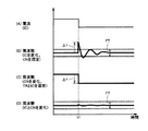
次に、電流調整コードICが切替わったときにおける発振周波数の跳びの抑制方法について説明する。まず、図3の容量部54によって発振周波数の調整が行なわれない場合、すなわち、発振周波数の跳びが抑制されない場合を説明する。
以下、図11〜図15を参照して、電流調整コードICの初期値を“00”、キャンセルコードCNの初期値を“n0”(n0は、10ビットの2進数を意味する)とし、電流調整コードICを初期値“00”から“01”に切替えたとき、切替後に供給すべきキャンセルコードCNの値を決定する手順について説明する。
図16は、この発明の実施の形態2による局部発振器26Aおよび制御部12の構成を示すブロック図である。図16の局部発振器26Aは、デジタルローパスフィルタ62Aの構成が実施の形態1のデジタルローパスフィルタ62と異なる。その他の局部発振器26Aの構成および制御部12の構成は、図2および図10で説明した実施の形態1の場合と同じであるので、同一または相当する部分には同一の参照符号を付して説明を繰返さない。
図20は、この発明の実施の形態3による局部発振器26Bおよび制御部12Aの構成を示すブロック図である。図20の局部発振器26Bは、切替部SW1を含まない点で図16の局部発振器26Aと異なる。実施の形態3の場合には、キャリブレーション時にもデジタルローパスフィルタ62AからLC発振器50にトラッキングコードTRが出力される。
実施の形態4では、図3で説明したLC発振器50の変形例について説明する。
PLL回路のロック外れは、分周器の駆動電流量を切替えることによってもLC発振器の負荷が変動するので生じることがある。さらには、時分割復信(TDD:Time Division Duplex)において送受信の切替を行なうときに、送信出力段の増幅アンプをオンまたはオフに切替えた場合にも、電源ラインの電圧変動によってPLL回路のロック外れが生じることがある。実施の形態1〜4で説明した発振周波数の跳びの抑制方法は、上記の場合に対しても適用することができる。
Claims (7)
- 半導体装置であって、
制御発振器を備え、前記制御発振器は、
1または複数のインダクタおよび容量値が変更可能な第1の容量部を含む共振回路と、
前記共振回路と接続され、前記共振回路の共振周波数に対応した発振周波数を有する局部発振信号を出力する増幅部と、
前記増幅部に供給する駆動電流の値を調整する電流調整部とを含み、
前記半導体装置は、
前記局部発振信号を分周して出力する分周器と、
前記分周器の出力と与えられた基準信号との位相差に応じた信号を出力する位相比較器と、
前記位相比較器の出力の高周波成分を除去することによってフィードバック信号を生成するフィルタ部と、
前記第1の容量部の容量値および前記電流調整部を制御する制御部とをさらに備え、
前記共振回路は、前記フィードバック信号の値に応じて容量値が変化する第2の容量部をさらに含み、
前記制御部は、前記増幅部に供給する駆動電流の値を変更するように前記電流調整部に指令したときには、前記発振周波数を一定に保つように前記第1の容量部の容量値を変更し、
前記半導体装置は、
与えられたベースバンド信号によって前記局部発振信号を変調して出力する変調器と、
前記変調器の出力を増幅する、ゲインを調整可能なアンプとをさらに備える、半導体装置。 - 前記制御部は、前記アンプのゲインに応じて前記増幅部に供給する駆動電流の値を変更するように前記電流調整部に指令する、請求項1に記載の半導体装置。
- 前記半導体装置は、前記フィルタ部と前記制御発振器との間の前記フィードバック信号の経路に設けられ、前記フィードバック信号および予め定める一定信号のいずれか一方を前記制御発振器の前記第2の容量部に供給する切替部をさらに含み、
前記第1の容量部の容量値は、前記制御部で生成された第1の制御信号の値に応じて変化し、
前記電流調整部は、前記制御部で生成された第2の制御信号の値に応じて前記増幅部に供給する駆動電流の値を調整し、
前記制御部は、キャリブレーション時に、前記切替部を切替えることによって前記一定信号を前記第2の容量部に供給した状態で前記第2の制御信号の値を変化させ、前記制御部は、前記第2の制御信号の値を変化させた前後で検出された前記局部発振信号の周波数が等しくなるように、前記第2の制御信号の値を変化させた後に供給する前記第1の制御信号の値を決定し、前記制御部は、決定した前記第1の制御信号の値を前記第2の制御信号の値の変化に対応付けてテーブルとして記憶し、
前記制御部は、前記フィードバック信号が前記切替部を介して前記制御発振器に供給される通常動作時において前記第2の制御信号の値を変化させる場合には、前記第2の制御信号の値を変化させた後に供給する前記第1の制御信号の値を前記テーブルに基づいて決定する、請求項1に記載の半導体装置。 - 前記第1の容量部の容量値は、前記制御部で生成された第1の制御信号の値に応じて変化し、
前記電流調整部は、前記制御部で生成された第2の制御信号の値に応じて前記増幅部に供給する駆動電流の値を調整し、
前記制御部は、キャリブレーション時に、前記第2の制御信号の値を変化させ、前記制御部は、前記第2の制御信号の値を変化させた前後で検出された前記フィードバック信号の値が等しくなるように、前記第2の制御信号の値を変化させた後に供給する前記第1の制御信号の値を決定し、前記制御部は、決定した前記第1の制御信号の値を前記第2の制御信号の値の変化に対応付けてテーブルとして記憶し、
前記制御部は、通常動作時に前記第2の制御信号の値を変化させる場合には、前記第2の制御信号の値を変化させた後に供給する前記第1の制御信号の値を前記テーブルに基づいて決定する、請求項1に記載の半導体装置。 - 前記フィルタ部は、デジタル回路によって構成され、前記制御部からの指令に応じて通過帯域幅を変更可能であり、
前記制御部は、前記増幅部に供給する駆動電流の値を変更するように前記電流調整部に指令したときには、前記フィルタ部の通過帯域幅を通常の帯域幅よりも増加させる、請求項1に記載の半導体装置。 - 半導体装置であって、
制御発振器を備え、前記制御発振器は、
1または複数のインダクタおよび容量値が変更可能な第1の容量部を含む共振回路と、
前記共振回路と接続され、前記共振回路の共振周波数に対応した発振周波数を有する局部発振信号を出力する増幅部と、
前記増幅部に供給する駆動電流の値を調整する電流調整部とを含み、
前記半導体装置は、
前記局部発振信号を分周して出力する分周器と、
前記分周器の出力と与えられた基準信号との位相差に応じた信号を出力する位相比較器と、
前記位相比較器の出力の高周波成分を除去することによってフィードバック信号を生成するフィルタ部と、
前記第1の容量部の容量値および前記電流調整部を制御する制御部とをさらに備え、
前記共振回路は、
前記フィードバック信号の値に応じて容量値が変化する第2の容量部と、
前記制御部の指令に応じて容量値が変化する第3の容量部とをさらに含み、
前記制御部は、前記第3の容量部の容量値を一定に保った状態で、前記増幅部に供給する駆動電流の値を変更するように前記電流調整部に指令したときには、前記発振周波数を一定に保つように前記第1の容量部の容量値を変更し、
前記半導体装置は、
与えられたベースバンド信号によって前記局部発振信号を変調して出力する変調器と、
前記変調器の出力を増幅する、ゲインを調整可能なアンプとをさらに備える、半導体装置。 - 半導体装置であって、
制御発振器を備え、前記制御発振器は、
1または複数のインダクタおよび容量値が変更可能な第1の容量部を含む共振回路と、
前記共振回路と接続され、前記共振回路の共振周波数に対応した発振周波数を有する局部発振信号を出力する増幅部と、
前記増幅部に供給する駆動電流の値を調整する電流調整部とを含み、
前記半導体装置は、
前記局部発振信号を分周して出力する分周器と、
前記分周器の出力と与えられた基準信号との位相差に応じた信号を出力する位相比較器と、
前記位相比較器の出力の高周波成分を除去することによってフィードバック信号を生成するフィルタ部と、
前記第1の容量部の容量値および前記電流調整部を制御する制御部とをさらに備え、
前記共振回路は、前記フィードバック信号の値に応じて容量値が変化する第2の容量部をさらに含み、
前記制御部は、第1の制御信号および第2の制御信号を生成し、
前記第1の容量部の容量値は、前記第1の制御信号と前記第2の制御信号とを加算した信号の値に応じて変化し、
前記制御部は、前記第2の制御信号を一定に保った状態で、前記増幅部に供給する駆動電流の値を変更するように前記電流調整部に指令したときには、前記発振周波数を一定に保つように前記第1の制御信号の値を変更し、
前記半導体装置は、
与えられたベースバンド信号によって前記局部発振信号を変調して出力する変調器と、
前記変調器の出力を増幅する、ゲインを調整可能なアンプとをさらに備える、半導体装置。
Applications Claiming Priority (1)
| Application Number | Priority Date | Filing Date | Title |
|---|---|---|---|
| PCT/JP2011/051458 WO2012101774A1 (ja) | 2011-01-26 | 2011-01-26 | 半導体装置 |
Publications (2)
| Publication Number | Publication Date |
|---|---|
| JPWO2012101774A1 JPWO2012101774A1 (ja) | 2014-06-30 |
| JP5668082B2 true JP5668082B2 (ja) | 2015-02-12 |
Family
ID=46580381
Family Applications (1)
| Application Number | Title | Priority Date | Filing Date |
|---|---|---|---|
| JP2012554564A Expired - Fee Related JP5668082B2 (ja) | 2011-01-26 | 2011-01-26 | 半導体装置 |
Country Status (3)
| Country | Link |
|---|---|
| US (2) | US9154143B2 (ja) |
| JP (1) | JP5668082B2 (ja) |
| WO (1) | WO2012101774A1 (ja) |
Cited By (3)
| Publication number | Priority date | Publication date | Assignee | Title |
|---|---|---|---|---|
| US10419009B2 (en) | 2017-06-15 | 2019-09-17 | Renesas Electronics Corporation | Radio signal processing device, semiconductor device, and oscillation frequency variation correction method |
| US10554173B2 (en) | 2015-11-18 | 2020-02-04 | Socionext Inc. | Voltage controlled oscillator and PLL circuit |
| US11038462B2 (en) | 2017-12-11 | 2021-06-15 | Sony Semiconductor Solutions Corporation | Semiconductor device and wireless communication apparatus |
Families Citing this family (23)
| Publication number | Priority date | Publication date | Assignee | Title |
|---|---|---|---|---|
| JP5975912B2 (ja) * | 2013-03-18 | 2016-08-23 | ルネサスエレクトロニクス株式会社 | 高周波信号処理装置 |
| US9602113B2 (en) * | 2014-08-27 | 2017-03-21 | Qualcomm Incorporated | Fast frequency throttling and re-locking technique for phase-locked loops |
| US10374511B2 (en) * | 2015-01-29 | 2019-08-06 | The Regents Of The University Of California | Switched capacitor DC-to-DC converter and power conversion control methods |
| US9680480B1 (en) | 2016-07-29 | 2017-06-13 | Movellus Circuits, Inc. | Fractional and reconfigurable digital phase-locked loop |
| US9705516B1 (en) * | 2016-07-29 | 2017-07-11 | Movellus Circuits, Inc. | Reconfigurable phase-locked loop with optional LC oscillator capability |
| US9762249B1 (en) | 2016-07-29 | 2017-09-12 | Movellus Circuits, Inc. | Reconfigurable phase-locked loop |
| US10158365B2 (en) | 2016-07-29 | 2018-12-18 | Movellus Circuits, Inc. | Digital, reconfigurable frequency and delay generator with phase measurement |
| US9698798B1 (en) * | 2016-07-29 | 2017-07-04 | Movellus Circuits, Inc. | Digital controller for a phase-locked loop |
| US10614182B2 (en) | 2016-10-19 | 2020-04-07 | Movellus Circuits, Inc. | Timing analysis for electronic design automation of parallel multi-state driver circuits |
| US10050634B1 (en) * | 2017-02-10 | 2018-08-14 | Apple Inc. | Quantization noise cancellation for fractional-N phased-locked loop |
| US10740526B2 (en) | 2017-08-11 | 2020-08-11 | Movellus Circuits, Inc. | Integrated circuit design system with automatic timing margin reduction |
| JP7193914B2 (ja) * | 2017-11-17 | 2022-12-21 | ローム株式会社 | 可変遅延回路、pll周波数シンセサイザ、電子機器 |
| US10594323B2 (en) | 2018-06-13 | 2020-03-17 | Movellus Circuits, Inc. | Locked loop circuit and method with digitally-controlled oscillator (DCO) gain normalization |
| US11496139B2 (en) | 2018-06-13 | 2022-11-08 | Movellus Circuits, Inc. | Frequency measurement circuit with adaptive accuracy |
| US11070215B2 (en) | 2018-06-13 | 2021-07-20 | Movellus Circuits, Inc. | Locked loop circuit and method with digitally-controlled oscillator (DCO) gain normalization |
| US11493950B2 (en) | 2018-06-13 | 2022-11-08 | Movellus Circuits, Inc. | Frequency counter circuit for detecting timing violations |
| KR102681257B1 (ko) * | 2018-12-27 | 2024-07-03 | 에스케이하이닉스 주식회사 | 반도체장치 |
| US10536153B1 (en) * | 2019-06-28 | 2020-01-14 | Dialog Semiconductor B.V. | Signal generator |
| JP7388240B2 (ja) * | 2020-02-27 | 2023-11-29 | セイコーエプソン株式会社 | チャージポンプ回路、pll回路および発振器 |
| US11239849B2 (en) | 2020-04-06 | 2022-02-01 | Movellus Circuits Inc. | Locked loop circuit and method with multi-phase synchronization |
| JP2021190779A (ja) * | 2020-05-27 | 2021-12-13 | ソニーセミコンダクタソリューションズ株式会社 | Pll回路 |
| US11979165B1 (en) | 2022-11-17 | 2024-05-07 | Movellus Circuits Inc. | Frequency multiplier circuit with programmable frequency transition controller |
| US11831318B1 (en) | 2022-11-17 | 2023-11-28 | Movellus Circuits Inc. | Frequency multiplier system with multi-transition controller |
Citations (8)
| Publication number | Priority date | Publication date | Assignee | Title |
|---|---|---|---|---|
| JPH01183920A (ja) * | 1988-01-19 | 1989-07-21 | Nec Corp | 送信機 |
| JPH05175858A (ja) * | 1991-12-25 | 1993-07-13 | Japan Radio Co Ltd | Pll回路 |
| US5900785A (en) * | 1996-11-13 | 1999-05-04 | Ericsson Inc. | System and method for offsetting load switching transients in a frequency synthesizer |
| US6546060B1 (en) * | 1998-04-23 | 2003-04-08 | General Research Of Electronics, Inc. | Direct modulating FSK transmitter for MCA |
| JP2005318509A (ja) * | 2004-03-31 | 2005-11-10 | Nec Compound Semiconductor Devices Ltd | Pll周波数シンセサイザ回路及びその周波数チューニング方法 |
| WO2006055792A1 (en) * | 2004-11-19 | 2006-05-26 | Qualcomm Incorporated | Adjustable-bias vco |
| JP2010278491A (ja) * | 2009-05-26 | 2010-12-09 | Renesas Electronics Corp | 周波数シンセサイザ |
| JP2011502403A (ja) * | 2007-10-25 | 2011-01-20 | クゥアルコム・インコーポレイテッド | 位相ロック・ループにおけるvcoの動的バイアス印加 |
Family Cites Families (14)
| Publication number | Priority date | Publication date | Assignee | Title |
|---|---|---|---|---|
| JPH03196706A (ja) | 1989-12-26 | 1991-08-28 | Matsushita Electric Ind Co Ltd | 発振回路 |
| JP3434794B2 (ja) | 2000-10-05 | 2003-08-11 | 山形日本電気株式会社 | Pll回路 |
| JP4540247B2 (ja) | 2001-04-13 | 2010-09-08 | 日本テキサス・インスツルメンツ株式会社 | Pll回路 |
| GB0126632D0 (en) | 2001-11-06 | 2002-01-02 | Hitachi Ltd | A communication semiconductor integrated circuit device and a wireless communication system |
| US6838951B1 (en) * | 2002-06-12 | 2005-01-04 | Rf Micro Devices, Inc. | Frequency synthesizer having VCO bias current compensation |
| JP2004266571A (ja) * | 2003-02-28 | 2004-09-24 | Nec Electronics Corp | 電圧制御発振器 |
| JP3840468B2 (ja) | 2003-09-29 | 2006-11-01 | 松下電器産業株式会社 | Pll周波数シンセサイザ |
| JP2005109618A (ja) * | 2003-09-29 | 2005-04-21 | Renesas Technology Corp | 通信用半導体集積回路および携帯端末システム |
| EP1583221A1 (en) | 2004-03-31 | 2005-10-05 | NEC Compound Semiconductor Devices, Ltd. | PLL frequency synthesizer circuit and frequency tuning method thereof |
| JP2007074436A (ja) | 2005-09-07 | 2007-03-22 | Asahi Kasei Microsystems Kk | 発振回路 |
| JP5005455B2 (ja) | 2007-07-23 | 2012-08-22 | ルネサスエレクトロニクス株式会社 | 半導体集積回路 |
| JP2009182918A (ja) | 2008-02-01 | 2009-08-13 | Toyota Industries Corp | 電圧制御発振回路 |
| JP4625849B2 (ja) | 2008-02-25 | 2011-02-02 | 株式会社東芝 | 発振器制御装置 |
| US8275331B2 (en) * | 2009-04-21 | 2012-09-25 | Qualcomm, Incorporated | PA gain state switching based on waveform linearity |
-
2011
- 2011-01-26 JP JP2012554564A patent/JP5668082B2/ja not_active Expired - Fee Related
- 2011-01-26 WO PCT/JP2011/051458 patent/WO2012101774A1/ja active Application Filing
- 2011-01-26 US US13/982,249 patent/US9154143B2/en not_active Expired - Fee Related
-
2015
- 2015-09-02 US US14/843,864 patent/US20150381344A1/en not_active Abandoned
Patent Citations (8)
| Publication number | Priority date | Publication date | Assignee | Title |
|---|---|---|---|---|
| JPH01183920A (ja) * | 1988-01-19 | 1989-07-21 | Nec Corp | 送信機 |
| JPH05175858A (ja) * | 1991-12-25 | 1993-07-13 | Japan Radio Co Ltd | Pll回路 |
| US5900785A (en) * | 1996-11-13 | 1999-05-04 | Ericsson Inc. | System and method for offsetting load switching transients in a frequency synthesizer |
| US6546060B1 (en) * | 1998-04-23 | 2003-04-08 | General Research Of Electronics, Inc. | Direct modulating FSK transmitter for MCA |
| JP2005318509A (ja) * | 2004-03-31 | 2005-11-10 | Nec Compound Semiconductor Devices Ltd | Pll周波数シンセサイザ回路及びその周波数チューニング方法 |
| WO2006055792A1 (en) * | 2004-11-19 | 2006-05-26 | Qualcomm Incorporated | Adjustable-bias vco |
| JP2011502403A (ja) * | 2007-10-25 | 2011-01-20 | クゥアルコム・インコーポレイテッド | 位相ロック・ループにおけるvcoの動的バイアス印加 |
| JP2010278491A (ja) * | 2009-05-26 | 2010-12-09 | Renesas Electronics Corp | 周波数シンセサイザ |
Non-Patent Citations (1)
| Title |
|---|
| JPN6011018668; Liangge Xu, et al: 'A 2.4-GHz low-power all-digital phase-locked loop' Custom Integrated Circuits Conference, 2009. CICC '09. IEEE , 20090913, pp.331-pp.334 * |
Cited By (3)
| Publication number | Priority date | Publication date | Assignee | Title |
|---|---|---|---|---|
| US10554173B2 (en) | 2015-11-18 | 2020-02-04 | Socionext Inc. | Voltage controlled oscillator and PLL circuit |
| US10419009B2 (en) | 2017-06-15 | 2019-09-17 | Renesas Electronics Corporation | Radio signal processing device, semiconductor device, and oscillation frequency variation correction method |
| US11038462B2 (en) | 2017-12-11 | 2021-06-15 | Sony Semiconductor Solutions Corporation | Semiconductor device and wireless communication apparatus |
Also Published As
| Publication number | Publication date |
|---|---|
| US9154143B2 (en) | 2015-10-06 |
| US20130300477A1 (en) | 2013-11-14 |
| US20150381344A1 (en) | 2015-12-31 |
| JPWO2012101774A1 (ja) | 2014-06-30 |
| WO2012101774A1 (ja) | 2012-08-02 |
Similar Documents
| Publication | Publication Date | Title |
|---|---|---|
| JP5668082B2 (ja) | 半導体装置 | |
| KR101191575B1 (ko) | 프로그램 가능 2점 주파수 합성기 아키텍처, 프로그램 가능 분수 n 분할기, 주파수 합성기 및 주파수 합성기 제어 방법 | |
| US10008980B2 (en) | Wideband digitally controlled injection-locked oscillator | |
| Lee et al. | A/spl Sigma/-/spl Delta/fractional-N frequency synthesizer using a wide-band integrated VCO and a fast AFC technique for GSM/GPRS/WCDMA applications | |
| KR101296311B1 (ko) | 다수의 조정 루프들을 갖는 주파수 합성기 | |
| CA2735676C (en) | Divide-by-three quadrature frequency divider | |
| CN104836580B (zh) | 任意相位轨迹频率合成器 | |
| US8553827B2 (en) | ADC-based mixed-mode digital phase-locked loop | |
| US9344100B2 (en) | Reconfigurable local oscillator for optimal noise performance in a multi-standard transceiver | |
| US7884655B2 (en) | Control circuitry | |
| US11411567B2 (en) | Phase interpolation-based fractional-N sampling phase-locked loop | |
| KR20120024680A (ko) | 어큐물레이터 및 위상-대-디지털 컨버터를 사용하는 투-포인트 변조를 갖는 디지털 위상-고정 루프 | |
| Vlachogiannakis et al. | A self-calibrated fractional-N PLL for WiFi 6/802.11 ax in 28nm FDSOI CMOS | |
| Lin et al. | Spur minimization techniques for ultra-low-power injection-locked transmitters | |
| CN101505149A (zh) | 本地信号发生电路 | |
| US9088285B2 (en) | Dynamic divider having interlocking circuit | |
| WO2011002944A1 (en) | Adc-based mixed-mode digital phase-locked loop | |
| Farazian et al. | Fast hopping frequency generation in digital CMOS | |
| Lee et al. | A 0.13-μm CMOS Σ-Δ frequency synthesizer with an area optimizing LPF, fast AFC time, and a wideband VCO for WCDMA/GSM/GPRS/EDGE applications | |
| JP2023548568A (ja) | 外部発振器の制御及び較正 | |
| Xu | A Study of Fractional Spur Suppression Techniques in Digital Phase-Locked Loops | |
| Soldner | Design of a Delta-sigma fractional-N PLL frequency synthesizer at 1.43 GHz | |
| Cheng et al. | A 2.4-GHz ISM band delta-sigma fractional-n frequency synthesizer with automatic calibration technique | |
| WO2024245537A1 (en) | Phase locked loop system and method for tuning oscillator | |
| Easwaran et al. | Specification driven design of Phase locked loops |
Legal Events
| Date | Code | Title | Description |
|---|---|---|---|
| A131 | Notification of reasons for refusal |
Free format text: JAPANESE INTERMEDIATE CODE: A131 Effective date: 20140902 |
|
| A521 | Request for written amendment filed |
Free format text: JAPANESE INTERMEDIATE CODE: A523 Effective date: 20141031 |
|
| TRDD | Decision of grant or rejection written | ||
| A01 | Written decision to grant a patent or to grant a registration (utility model) |
Free format text: JAPANESE INTERMEDIATE CODE: A01 Effective date: 20141209 |
|
| A61 | First payment of annual fees (during grant procedure) |
Free format text: JAPANESE INTERMEDIATE CODE: A61 Effective date: 20141215 |
|
| R150 | Certificate of patent or registration of utility model |
Ref document number: 5668082 Country of ref document: JP Free format text: JAPANESE INTERMEDIATE CODE: R150 |
|
| S531 | Written request for registration of change of domicile |
Free format text: JAPANESE INTERMEDIATE CODE: R313531 |
|
| R350 | Written notification of registration of transfer |
Free format text: JAPANESE INTERMEDIATE CODE: R350 |
|
| LAPS | Cancellation because of no payment of annual fees |