JP5645404B2 - High power insulated gate bipolar transistor - Google Patents
High power insulated gate bipolar transistor Download PDFInfo
- Publication number
- JP5645404B2 JP5645404B2 JP2009524593A JP2009524593A JP5645404B2 JP 5645404 B2 JP5645404 B2 JP 5645404B2 JP 2009524593 A JP2009524593 A JP 2009524593A JP 2009524593 A JP2009524593 A JP 2009524593A JP 5645404 B2 JP5645404 B2 JP 5645404B2
- Authority
- JP
- Japan
- Prior art keywords
- region
- type
- layer
- channel
- ohmic contact
- Prior art date
- Legal status (The legal status is an assumption and is not a legal conclusion. Google has not performed a legal analysis and makes no representation as to the accuracy of the status listed.)
- Active
Links
- 239000010410 layer Substances 0.000 claims description 141
- 108091006146 Channels Proteins 0.000 claims description 53
- 229910010271 silicon carbide Inorganic materials 0.000 claims description 43
- HBMJWWWQQXIZIP-UHFFFAOYSA-N silicon carbide Chemical compound [Si+]#[C-] HBMJWWWQQXIZIP-UHFFFAOYSA-N 0.000 claims description 38
- 239000000758 substrate Substances 0.000 claims description 16
- 239000002019 doping agent Substances 0.000 claims description 15
- PXHVJJICTQNCMI-UHFFFAOYSA-N Nickel Chemical compound [Ni] PXHVJJICTQNCMI-UHFFFAOYSA-N 0.000 claims description 10
- 229910052751 metal Inorganic materials 0.000 claims description 9
- 239000002184 metal Substances 0.000 claims description 9
- 239000011229 interlayer Substances 0.000 claims description 8
- 239000000463 material Substances 0.000 claims description 8
- 108010075750 P-Type Calcium Channels Proteins 0.000 claims description 6
- 229910052782 aluminium Inorganic materials 0.000 claims description 6
- 239000004020 conductor Substances 0.000 claims description 6
- XAGFODPZIPBFFR-UHFFFAOYSA-N aluminium Chemical compound [Al] XAGFODPZIPBFFR-UHFFFAOYSA-N 0.000 claims description 5
- 230000003750 conditioning effect Effects 0.000 claims description 4
- 229910052759 nickel Inorganic materials 0.000 claims description 3
- 238000000137 annealing Methods 0.000 description 36
- 238000000034 method Methods 0.000 description 19
- 150000002500 ions Chemical class 0.000 description 18
- OKTJSMMVPCPJKN-UHFFFAOYSA-N Carbon Chemical compound [C] OKTJSMMVPCPJKN-UHFFFAOYSA-N 0.000 description 16
- 229910002804 graphite Inorganic materials 0.000 description 16
- 239000010439 graphite Substances 0.000 description 16
- 238000000576 coating method Methods 0.000 description 13
- 230000000903 blocking effect Effects 0.000 description 12
- 239000011248 coating agent Substances 0.000 description 12
- 239000007943 implant Substances 0.000 description 12
- 230000008569 process Effects 0.000 description 9
- 238000012360 testing method Methods 0.000 description 9
- UFHFLCQGNIYNRP-UHFFFAOYSA-N Hydrogen Chemical compound [H][H] UFHFLCQGNIYNRP-UHFFFAOYSA-N 0.000 description 8
- VYPSYNLAJGMNEJ-UHFFFAOYSA-N Silicium dioxide Chemical compound O=[Si]=O VYPSYNLAJGMNEJ-UHFFFAOYSA-N 0.000 description 8
- 239000001257 hydrogen Substances 0.000 description 7
- 229910052739 hydrogen Inorganic materials 0.000 description 7
- 238000002513 implantation Methods 0.000 description 7
- 230000004913 activation Effects 0.000 description 6
- QVGXLLKOCUKJST-UHFFFAOYSA-N atomic oxygen Chemical compound [O] QVGXLLKOCUKJST-UHFFFAOYSA-N 0.000 description 6
- 230000003647 oxidation Effects 0.000 description 6
- 238000007254 oxidation reaction Methods 0.000 description 6
- 239000001301 oxygen Substances 0.000 description 6
- 229910052760 oxygen Inorganic materials 0.000 description 6
- XLYOFNOQVPJJNP-UHFFFAOYSA-N water Chemical compound O XLYOFNOQVPJJNP-UHFFFAOYSA-N 0.000 description 6
- 230000007423 decrease Effects 0.000 description 5
- 230000001939 inductive effect Effects 0.000 description 5
- 235000012239 silicon dioxide Nutrition 0.000 description 5
- IJGRMHOSHXDMSA-UHFFFAOYSA-N Atomic nitrogen Chemical compound N#N IJGRMHOSHXDMSA-UHFFFAOYSA-N 0.000 description 4
- MYMOFIZGZYHOMD-UHFFFAOYSA-N Dioxygen Chemical compound O=O MYMOFIZGZYHOMD-UHFFFAOYSA-N 0.000 description 4
- 238000013461 design Methods 0.000 description 4
- 229910001882 dioxygen Inorganic materials 0.000 description 4
- XUIMIQQOPSSXEZ-UHFFFAOYSA-N Silicon Chemical compound [Si] XUIMIQQOPSSXEZ-UHFFFAOYSA-N 0.000 description 3
- 230000015572 biosynthetic process Effects 0.000 description 3
- 238000002347 injection Methods 0.000 description 3
- 239000007924 injection Substances 0.000 description 3
- 238000004519 manufacturing process Methods 0.000 description 3
- 229910021420 polycrystalline silicon Inorganic materials 0.000 description 3
- 229920005591 polysilicon Polymers 0.000 description 3
- 229910052710 silicon Inorganic materials 0.000 description 3
- 239000010703 silicon Substances 0.000 description 3
- 239000000377 silicon dioxide Substances 0.000 description 3
- 229910000789 Aluminium-silicon alloy Inorganic materials 0.000 description 2
- XKRFYHLGVUSROY-UHFFFAOYSA-N Argon Chemical compound [Ar] XKRFYHLGVUSROY-UHFFFAOYSA-N 0.000 description 2
- 230000009471 action Effects 0.000 description 2
- 238000013459 approach Methods 0.000 description 2
- 239000003990 capacitor Substances 0.000 description 2
- 239000002775 capsule Substances 0.000 description 2
- 239000000969 carrier Substances 0.000 description 2
- 230000008859 change Effects 0.000 description 2
- 238000011161 development Methods 0.000 description 2
- 230000018109 developmental process Effects 0.000 description 2
- 238000005538 encapsulation Methods 0.000 description 2
- 239000007789 gas Substances 0.000 description 2
- 238000010438 heat treatment Methods 0.000 description 2
- 230000001965 increasing effect Effects 0.000 description 2
- 210000003127 knee Anatomy 0.000 description 2
- 239000000203 mixture Substances 0.000 description 2
- 229910052757 nitrogen Inorganic materials 0.000 description 2
- 230000001698 pyrogenic effect Effects 0.000 description 2
- 239000010453 quartz Substances 0.000 description 2
- -1 region Substances 0.000 description 2
- 238000009279 wet oxidation reaction Methods 0.000 description 2
- JBRZTFJDHDCESZ-UHFFFAOYSA-N AsGa Chemical compound [As]#[Ga] JBRZTFJDHDCESZ-UHFFFAOYSA-N 0.000 description 1
- ZOXJGFHDIHLPTG-UHFFFAOYSA-N Boron Chemical compound [B] ZOXJGFHDIHLPTG-UHFFFAOYSA-N 0.000 description 1
- 241000408659 Darpa Species 0.000 description 1
- 229910000807 Ga alloy Inorganic materials 0.000 description 1
- 229910002601 GaN Inorganic materials 0.000 description 1
- 229910001218 Gallium arsenide Inorganic materials 0.000 description 1
- JMASRVWKEDWRBT-UHFFFAOYSA-N Gallium nitride Chemical compound [Ga]#N JMASRVWKEDWRBT-UHFFFAOYSA-N 0.000 description 1
- 229910005883 NiSi Inorganic materials 0.000 description 1
- 229910004298 SiO 2 Inorganic materials 0.000 description 1
- 239000000956 alloy Substances 0.000 description 1
- 229910052786 argon Inorganic materials 0.000 description 1
- 238000004380 ashing Methods 0.000 description 1
- 229910052796 boron Inorganic materials 0.000 description 1
- 230000015556 catabolic process Effects 0.000 description 1
- 239000013078 crystal Substances 0.000 description 1
- 230000007547 defect Effects 0.000 description 1
- 238000010586 diagram Methods 0.000 description 1
- 238000010891 electric arc Methods 0.000 description 1
- 229910052732 germanium Inorganic materials 0.000 description 1
- GNPVGFCGXDBREM-UHFFFAOYSA-N germanium atom Chemical compound [Ge] GNPVGFCGXDBREM-UHFFFAOYSA-N 0.000 description 1
- 150000002431 hydrogen Chemical class 0.000 description 1
- 239000011261 inert gas Substances 0.000 description 1
- 238000005468 ion implantation Methods 0.000 description 1
- 238000005259 measurement Methods 0.000 description 1
- 238000001465 metallisation Methods 0.000 description 1
- 230000035515 penetration Effects 0.000 description 1
- RVZRBWKZFJCCIB-UHFFFAOYSA-N perfluorotributylamine Chemical compound FC(F)(F)C(F)(F)C(F)(F)C(F)(F)N(C(F)(F)C(F)(F)C(F)(F)C(F)(F)F)C(F)(F)C(F)(F)C(F)(F)C(F)(F)F RVZRBWKZFJCCIB-UHFFFAOYSA-N 0.000 description 1
- 238000012545 processing Methods 0.000 description 1
- 238000004151 rapid thermal annealing Methods 0.000 description 1
- 238000011084 recovery Methods 0.000 description 1
- 230000009467 reduction Effects 0.000 description 1
- 239000004065 semiconductor Substances 0.000 description 1
Images


Classifications
-
- H—ELECTRICITY
- H10—SEMICONDUCTOR DEVICES; ELECTRIC SOLID-STATE DEVICES NOT OTHERWISE PROVIDED FOR
- H10D—INORGANIC ELECTRIC SEMICONDUCTOR DEVICES
- H10D10/00—Bipolar junction transistors [BJT]
-
- H—ELECTRICITY
- H10—SEMICONDUCTOR DEVICES; ELECTRIC SOLID-STATE DEVICES NOT OTHERWISE PROVIDED FOR
- H10D—INORGANIC ELECTRIC SEMICONDUCTOR DEVICES
- H10D12/00—Bipolar devices controlled by the field effect, e.g. insulated-gate bipolar transistors [IGBT]
- H10D12/01—Manufacture or treatment
- H10D12/031—Manufacture or treatment of IGBTs
-
- H—ELECTRICITY
- H01—ELECTRIC ELEMENTS
- H01L—SEMICONDUCTOR DEVICES NOT COVERED BY CLASS H10
- H01L21/00—Processes or apparatus adapted for the manufacture or treatment of semiconductor or solid state devices or of parts thereof
- H01L21/02—Manufacture or treatment of semiconductor devices or of parts thereof
- H01L21/02104—Forming layers
- H01L21/02365—Forming inorganic semiconducting materials on a substrate
- H01L21/02367—Substrates
- H01L21/0237—Materials
- H01L21/02373—Group 14 semiconducting materials
- H01L21/02378—Silicon carbide
-
- H—ELECTRICITY
- H01—ELECTRIC ELEMENTS
- H01L—SEMICONDUCTOR DEVICES NOT COVERED BY CLASS H10
- H01L21/00—Processes or apparatus adapted for the manufacture or treatment of semiconductor or solid state devices or of parts thereof
- H01L21/02—Manufacture or treatment of semiconductor devices or of parts thereof
- H01L21/02104—Forming layers
- H01L21/02365—Forming inorganic semiconducting materials on a substrate
- H01L21/02518—Deposited layers
- H01L21/02521—Materials
- H01L21/02524—Group 14 semiconducting materials
- H01L21/02529—Silicon carbide
-
- H—ELECTRICITY
- H01—ELECTRIC ELEMENTS
- H01L—SEMICONDUCTOR DEVICES NOT COVERED BY CLASS H10
- H01L21/00—Processes or apparatus adapted for the manufacture or treatment of semiconductor or solid state devices or of parts thereof
- H01L21/02—Manufacture or treatment of semiconductor devices or of parts thereof
- H01L21/04—Manufacture or treatment of semiconductor devices or of parts thereof the devices having potential barriers, e.g. a PN junction, depletion layer or carrier concentration layer
- H01L21/0445—Manufacture or treatment of semiconductor devices or of parts thereof the devices having potential barriers, e.g. a PN junction, depletion layer or carrier concentration layer the devices having semiconductor bodies comprising crystalline silicon carbide
- H01L21/0455—Making n or p doped regions or layers, e.g. using diffusion
- H01L21/046—Making n or p doped regions or layers, e.g. using diffusion using ion implantation
-
- H—ELECTRICITY
- H01—ELECTRIC ELEMENTS
- H01L—SEMICONDUCTOR DEVICES NOT COVERED BY CLASS H10
- H01L21/00—Processes or apparatus adapted for the manufacture or treatment of semiconductor or solid state devices or of parts thereof
- H01L21/02—Manufacture or treatment of semiconductor devices or of parts thereof
- H01L21/04—Manufacture or treatment of semiconductor devices or of parts thereof the devices having potential barriers, e.g. a PN junction, depletion layer or carrier concentration layer
- H01L21/0445—Manufacture or treatment of semiconductor devices or of parts thereof the devices having potential barriers, e.g. a PN junction, depletion layer or carrier concentration layer the devices having semiconductor bodies comprising crystalline silicon carbide
- H01L21/048—Making electrodes
- H01L21/049—Conductor-insulator-semiconductor electrodes, e.g. MIS contacts
-
- H—ELECTRICITY
- H01—ELECTRIC ELEMENTS
- H01L—SEMICONDUCTOR DEVICES NOT COVERED BY CLASS H10
- H01L21/00—Processes or apparatus adapted for the manufacture or treatment of semiconductor or solid state devices or of parts thereof
- H01L21/02—Manufacture or treatment of semiconductor devices or of parts thereof
- H01L21/04—Manufacture or treatment of semiconductor devices or of parts thereof the devices having potential barriers, e.g. a PN junction, depletion layer or carrier concentration layer
- H01L21/18—Manufacture or treatment of semiconductor devices or of parts thereof the devices having potential barriers, e.g. a PN junction, depletion layer or carrier concentration layer the devices having semiconductor bodies comprising elements of Group IV of the Periodic Table or AIIIBV compounds with or without impurities, e.g. doping materials
- H01L21/22—Diffusion of impurity materials, e.g. doping materials, electrode materials, into or out of a semiconductor body, or between semiconductor regions; Interactions between two or more impurities; Redistribution of impurities
- H01L21/225—Diffusion of impurity materials, e.g. doping materials, electrode materials, into or out of a semiconductor body, or between semiconductor regions; Interactions between two or more impurities; Redistribution of impurities using diffusion into or out of a solid from or into a solid phase, e.g. a doped oxide layer
- H01L21/2251—Diffusion into or out of group IV semiconductors
- H01L21/2254—Diffusion into or out of group IV semiconductors from or through or into an applied layer, e.g. photoresist, nitrides
-
- H—ELECTRICITY
- H01—ELECTRIC ELEMENTS
- H01L—SEMICONDUCTOR DEVICES NOT COVERED BY CLASS H10
- H01L21/00—Processes or apparatus adapted for the manufacture or treatment of semiconductor or solid state devices or of parts thereof
- H01L21/02—Manufacture or treatment of semiconductor devices or of parts thereof
- H01L21/04—Manufacture or treatment of semiconductor devices or of parts thereof the devices having potential barriers, e.g. a PN junction, depletion layer or carrier concentration layer
- H01L21/18—Manufacture or treatment of semiconductor devices or of parts thereof the devices having potential barriers, e.g. a PN junction, depletion layer or carrier concentration layer the devices having semiconductor bodies comprising elements of Group IV of the Periodic Table or AIIIBV compounds with or without impurities, e.g. doping materials
- H01L21/26—Bombardment with radiation
- H01L21/263—Bombardment with radiation with high-energy radiation
- H01L21/265—Bombardment with radiation with high-energy radiation producing ion implantation
- H01L21/26506—Bombardment with radiation with high-energy radiation producing ion implantation in group IV semiconductors
- H01L21/26513—Bombardment with radiation with high-energy radiation producing ion implantation in group IV semiconductors of electrically active species
-
- H—ELECTRICITY
- H01—ELECTRIC ELEMENTS
- H01L—SEMICONDUCTOR DEVICES NOT COVERED BY CLASS H10
- H01L21/00—Processes or apparatus adapted for the manufacture or treatment of semiconductor or solid state devices or of parts thereof
- H01L21/02—Manufacture or treatment of semiconductor devices or of parts thereof
- H01L21/04—Manufacture or treatment of semiconductor devices or of parts thereof the devices having potential barriers, e.g. a PN junction, depletion layer or carrier concentration layer
- H01L21/18—Manufacture or treatment of semiconductor devices or of parts thereof the devices having potential barriers, e.g. a PN junction, depletion layer or carrier concentration layer the devices having semiconductor bodies comprising elements of Group IV of the Periodic Table or AIIIBV compounds with or without impurities, e.g. doping materials
- H01L21/30—Treatment of semiconductor bodies using processes or apparatus not provided for in groups H01L21/20 - H01L21/26
- H01L21/324—Thermal treatment for modifying the properties of semiconductor bodies, e.g. annealing, sintering
-
- H—ELECTRICITY
- H10—SEMICONDUCTOR DEVICES; ELECTRIC SOLID-STATE DEVICES NOT OTHERWISE PROVIDED FOR
- H10D—INORGANIC ELECTRIC SEMICONDUCTOR DEVICES
- H10D12/00—Bipolar devices controlled by the field effect, e.g. insulated-gate bipolar transistors [IGBT]
- H10D12/01—Manufacture or treatment
- H10D12/031—Manufacture or treatment of IGBTs
- H10D12/032—Manufacture or treatment of IGBTs of vertical IGBTs
-
- H—ELECTRICITY
- H10—SEMICONDUCTOR DEVICES; ELECTRIC SOLID-STATE DEVICES NOT OTHERWISE PROVIDED FOR
- H10D—INORGANIC ELECTRIC SEMICONDUCTOR DEVICES
- H10D12/00—Bipolar devices controlled by the field effect, e.g. insulated-gate bipolar transistors [IGBT]
- H10D12/411—Insulated-gate bipolar transistors [IGBT]
- H10D12/441—Vertical IGBTs
-
- H—ELECTRICITY
- H10—SEMICONDUCTOR DEVICES; ELECTRIC SOLID-STATE DEVICES NOT OTHERWISE PROVIDED FOR
- H10D—INORGANIC ELECTRIC SEMICONDUCTOR DEVICES
- H10D62/00—Semiconductor bodies, or regions thereof, of devices having potential barriers
- H10D62/10—Shapes, relative sizes or dispositions of the regions of the semiconductor bodies; Shapes of the semiconductor bodies
- H10D62/17—Semiconductor regions connected to electrodes not carrying current to be rectified, amplified or switched, e.g. channel regions
- H10D62/393—Body regions of DMOS transistors or IGBTs
-
- H—ELECTRICITY
- H10—SEMICONDUCTOR DEVICES; ELECTRIC SOLID-STATE DEVICES NOT OTHERWISE PROVIDED FOR
- H10D—INORGANIC ELECTRIC SEMICONDUCTOR DEVICES
- H10D62/00—Semiconductor bodies, or regions thereof, of devices having potential barriers
- H10D62/80—Semiconductor bodies, or regions thereof, of devices having potential barriers characterised by the materials
- H10D62/83—Semiconductor bodies, or regions thereof, of devices having potential barriers characterised by the materials being Group IV materials, e.g. B-doped Si or undoped Ge
- H10D62/832—Semiconductor bodies, or regions thereof, of devices having potential barriers characterised by the materials being Group IV materials, e.g. B-doped Si or undoped Ge being Group IV materials comprising two or more elements, e.g. SiGe
- H10D62/8325—Silicon carbide
Landscapes
- Engineering & Computer Science (AREA)
- Physics & Mathematics (AREA)
- Computer Hardware Design (AREA)
- Microelectronics & Electronic Packaging (AREA)
- Power Engineering (AREA)
- Condensed Matter Physics & Semiconductors (AREA)
- General Physics & Mathematics (AREA)
- Manufacturing & Machinery (AREA)
- Chemical & Material Sciences (AREA)
- High Energy & Nuclear Physics (AREA)
- Crystallography & Structural Chemistry (AREA)
- Toxicology (AREA)
- Health & Medical Sciences (AREA)
- Materials Engineering (AREA)
- Electrodes Of Semiconductors (AREA)
- Insulated Gate Type Field-Effect Transistor (AREA)
Description
米国政府の権利についての記述
本発明は、ONR/DARPAによって与えられた契約番号第N00014−05−C−0202号の下、米国政府の支援によってなされたものである。米国政府は本発明に関して一定の権利を有する。
Description of US Government Rights This invention was made with US government support under contract number N00014-05-C-0202 awarded by ONR / DARPA. The United States government has certain rights in this invention.
関連出願の相互参照および優先権の主張
本出願は、2006年8月17日に出願された「High Power Insulated Gate Bipolar Transistors」という名称の米国仮特許出願第60/838,249号に基づく利益および優先権を主張するものである。この仮出願の開示は、その全体が本明細書に記載されているかのように、参照によって本明細書に組み込まれる。
CROSS REFERENCE TO RELATED APPLICATIONS AND PRIORITY CLAIM This application is based on US Provisional Patent Application No. 60 / 838,249, filed August 17, 2006, entitled “High Power Insulated Gate Bipolar Transistors” and It claims priority. The disclosure of this provisional application is hereby incorporated by reference as if set forth in its entirety herein.
本発明は電子デバイスに関する。より具体的には、本発明は、高電力絶縁ゲート・バイポーラ・トランジスタに関する。 The present invention relates to an electronic device. More specifically, the present invention relates to high power insulated gate bipolar transistors.
炭化シリコン(SiC)を用いて製造されたパワー・デバイスは、SiCの高いクリティカル・フィールドおよび広いバンド・ギャップのため、シリコン上に製造されたパワー・デバイスと比較して、高速、高電力および/または高温用途に関して大きな利点を示すと予想される。約5kVを超える電圧などの高電圧をブロッキングする能力を有するデバイスでは、少数キャリアの注入に起因する導電率変調によってドリフト層の抵抗を低減させるために、バイポーラ動作を有することが望ましいことがある。しかしながら、炭化シリコン中に製造されたバイポーラ・デバイスの1つの技術的な難問は、時間の経過に伴う順方向電圧の低下であり、これはおそらく、炭化シリコンの単結晶内に底面転位(Basal Plane Dislocation:BPD)が存在することに起因する。したがって、高電力用途に対しては、SiCショットキー・ダイオード、MOSFETなどのユニポーラ・デバイスが一般に使用される。 Power devices manufactured using silicon carbide (SiC) are faster, higher power and / or higher compared to power devices manufactured on silicon due to the high critical field and wide band gap of SiC. Or expected to show significant advantages for high temperature applications. In devices that have the ability to block high voltages, such as voltages above about 5 kV, it may be desirable to have bipolar operation to reduce drift layer resistance through conductivity modulation due to minority carrier injection. However, one technical challenge of bipolar devices fabricated in silicon carbide is the decrease in forward voltage over time, which is probably a basal plane dislocation (Basal Plane) within the silicon carbide single crystal. This is due to the existence of Dislocation (BPD). Thus, for high power applications, unipolar devices such as SiC Schottky diodes and MOSFETs are commonly used.
10kVのブロッキング能力および約100mΩ×cm2の固有オン抵抗を有するSiC DMOSFETデバイスが製造された。DMOSFETデバイスは、それらの多数キャリア性のため、例えば100ns未満の非常に速いスイッチング速度を示すことができる。しかしながら、デバイスに求められるブロッキング電圧が例えば15kV以上と高くなるにつれ、それに対応してドリフト層の厚さが厚くなるため、MOSFETデバイスのオン抵抗が大幅に増大する可能性がある。高温では、バルク移動度が低下するために、この問題が悪化する可能性があり、これによって電力損が過大になる可能性がある。 A SiC DMOSFET device with a blocking capability of 10 kV and a specific on-resistance of about 100 mΩ × cm 2 was fabricated. DMOSFET devices can exhibit very fast switching speeds, eg, less than 100 ns, due to their majority carrier nature. However, as the blocking voltage required for the device increases to, for example, 15 kV or higher, the drift layer thickness correspondingly increases, and thus the on-resistance of the MOSFET device may increase significantly. At high temperatures, this problem can be exacerbated due to the decrease in bulk mobility, which can lead to excessive power loss.
SiC結晶材料成長の進歩によって、BPDに関係した問題を緩和するいくつかの方法が開発された。例えば、B.Hull、M.Das、J.Sumakeris、J.RichmondおよびS.Krishinaswami、「Drift−Free 10−kV,20−A 4H−SiC PiN Diodes」、Journal of Electrical Materials、第34巻、4号、2005年(非特許文献1)を参照されたい。これらの開発は、サイリスタ、GTOなどのSiCバイポーラ・デバイスの開発および/または潜在的応用を促進する可能性がある。たとえサイリスタおよび/またはGTOが低い順方向電圧降下を提供することができるとしても、それらは、ゲートの駆動および保護のために大きな整流回路を必要とする可能性がある。したがって、SiCバイポーラ・デバイスは、ゲート・ターンオフ能力を有することが望ましいことがある。それらの優れたオン状態特性のため、適度なスイッチング速度および/または優れたセーフ・オペレーション・エリア(safe−operation−area:SOA)を有する4H−SiC絶縁ゲート・バイポーラ・トランジスタ(insulated gate bipolar transistor:IGBT)は、電力スイッチング用途に対してますます適したものとなっている。 With advances in SiC crystal material growth, several methods have been developed to alleviate the problems associated with BPD. For example, B.I. Hull, M.M. Das, J .; Sumakeris, J. et al. Richmond and S.M. See Krishinawami, “Drift-Free 10-kV, 20-A 4H-SiC PiN Diodes”, Journal of Electrical Materials, Vol. 34, No. 4, 2005 (Non-patent Document 1). These developments may facilitate the development and / or potential application of SiC bipolar devices such as thyristors and GTOs. Even though thyristors and / or GTOs can provide low forward voltage drops, they can require large rectifier circuits for gate drive and protection. Thus, it may be desirable for a SiC bipolar device to have gate turn-off capability. Because of their excellent on-state characteristics, 4H-SiC insulated gate bipolar transistors with moderate switching speed and / or excellent safe-operation-area (SOA): IGBTs are becoming increasingly suitable for power switching applications.
いくつかの実施形態に基づく炭化シリコン・ベースの絶縁ゲート・バイポーラ・トランジスタ(IGBT)は、第1の導電型を有する炭化シリコン基板と、第1の導電型とは反対の第2の導電型を有する炭化シリコン・ドリフト層と、ドリフト層内にあって第1の導電型を有するウェル領域とを含む。ドリフト層上には、炭化シリコン・エピタキシャル・チャネル調整層があり、この炭化シリコン・エピタキシャル・チャネル調整層は第2の導電型を有する。エピタキシャル・チャネル調整層の表面からエピタキシャル・チャネル調整層を貫通してウェル領域内へエミッタ領域が延びる。エミッタ領域は第2の導電型を有し、エミッタ領域に隣接したウェル領域内にチャネル領域を少なくとも部分的に画定する。チャネル領域上にゲート酸化物層があり、ゲート酸化物層上にゲートがある。 A silicon carbide based insulated gate bipolar transistor (IGBT) according to some embodiments includes a silicon carbide substrate having a first conductivity type and a second conductivity type opposite to the first conductivity type. A silicon carbide drift layer and a well region in the drift layer and having a first conductivity type. A silicon carbide epitaxial channel adjustment layer is on the drift layer, and the silicon carbide epitaxial channel adjustment layer has the second conductivity type. An emitter region extends from the surface of the epitaxial channel adjustment layer through the epitaxial channel adjustment layer into the well region. The emitter region has a second conductivity type and at least partially defines a channel region in a well region adjacent to the emitter region. There is a gate oxide layer over the channel region and a gate over the gate oxide layer.
炭化シリコン・ドリフト層は、ウェル領域に隣接したJFET領域を含むことができる。エミッタ領域は、JFET領域から間隔を置いて配置することができ、エミッタ領域とJFET領域の間にチャネル領域を画定することができる。 The silicon carbide drift layer can include a JFET region adjacent to the well region. The emitter region can be spaced from the JFET region, and a channel region can be defined between the emitter region and the JFET region.
いくつかの実施形態では、第1の導電型をn型とすることができ、第2の導電型をp型とすることができる。 In some embodiments, the first conductivity type can be n-type and the second conductivity type can be p-type.
このトランジスタはさらに、チャネル調整層の表面からウェル領域内へ延びる第1の導電型のコネクタ領域と、コネクタ領域上の第1のオーミック・コンタクトと、エミッタ領域上にあって、第1のオーミック・コンタクトとは異なる材料を含む第2のオーミック・コンタクトと、第1のオーミック・コンタクトと第2のオーミック・コンタクトとを電気的に接続した金属オーバレイヤとを含むことができる。 The transistor further includes a connector region of a first conductivity type extending from the surface of the channel adjustment layer into the well region, a first ohmic contact on the connector region, and a first ohmic contact on the emitter region. A second ohmic contact including a material different from the contact and a metal overlayer electrically connecting the first ohmic contact and the second ohmic contact can be included.
第1のオーミック・コンタクトはニッケル・ベースの導電材料を含むことができ、第2のオーミック・コンタクトはアルミニウム・ベースの導電材料を含むことができる。 The first ohmic contact can include a nickel-based conductive material and the second ohmic contact can include an aluminum-based conductive material.
チャネル調整層は約0.25μm以上の厚さを有することができる。さらに、エミッタ領域の底面からウェル領域の底面までの距離は約0.45μm以上である。チャネル調整層は、約0.1μmから約0.5μmの厚さ、および約1×1016cm−3から約5×1018cm−3の正味ドーピング濃度を有することができる。 The channel adjustment layer may have a thickness of about 0.25 μm or more. Further, the distance from the bottom surface of the emitter region to the bottom surface of the well region is about 0.45 μm or more. The channel tuning layer can have a thickness of about 0.1 μm to about 0.5 μm and a net doping concentration of about 1 × 10 16 cm −3 to about 5 × 10 18 cm −3 .
本発明のいくつかの実施形態は、炭化シリコン内に絶縁ゲート・バイポーラ・トランジスタ(IGBT)デバイスを形成するいくつかの方法を提供する。これらの方法は、n型炭化シリコン基板上にp型炭化シリコン・ドリフト層を形成する工程、p型炭化シリコン・ドリフト層内にn型ウェルを形成する工程、及び、p型炭化シリコン・ドリフト層上とn型ウェル上とにp型チャネル調整層をエピタキシャル成長させる工程を含む。チャネル層を貫通して炭化シリコン層の表面のn型ウェル内へ延びるp型エミッタ領域を形成するために、p型ドーパント・イオンを注入することができる。p型エミッタ領域は、p型エミッタ領域に隣接したn型ウェル内にチャネル領域を少なくとも部分的に画定する。これらの方法はさらに、チャネル層を貫通して炭化シリコン層の表面のn型ウェル内へ延びるn型コネクタ領域を形成するために、n型ドーパント・イオンを注入する工程を含む。注入されたイオンはアニールされる。チャネル領域上にゲート酸化物層が形成され、ゲート酸化物層上にゲートが形成される。 Some embodiments of the present invention provide several methods of forming an insulated gate bipolar transistor (IGBT) device in silicon carbide. These methods include forming a p-type silicon carbide drift layer on an n-type silicon carbide substrate, forming an n-type well in the p-type silicon carbide drift layer, and a p-type silicon carbide drift layer. And a step of epitaxially growing a p-type channel adjustment layer on the n-type well and the n-type well. P-type dopant ions can be implanted to form a p-type emitter region that extends through the channel layer and into an n-type well on the surface of the silicon carbide layer. The p-type emitter region at least partially defines a channel region in an n-type well adjacent to the p-type emitter region. These methods further include implanting n-type dopant ions to form an n-type connector region that extends through the channel layer and into an n-type well on the surface of the silicon carbide layer. The implanted ions are annealed. A gate oxide layer is formed on the channel region, and a gate is formed on the gate oxide layer.
これらの方法はさらに、注入物を活性化させるために黒鉛コーティングを形成する工程、および注入されたイオンをアニールした後に黒鉛コーティングを除去する工程を含むことができる。注入されたイオンをアニールする工程は、炭化シリコン層および黒鉛コーティングをアニールする工程を含むことができる。これらの方法はさらに、注入されたイオンをアニールする前に黒鉛コーティングを結晶化させる工程を含むことができる。 These methods can further include forming a graphite coating to activate the implant, and removing the graphite coating after annealing the implanted ions. Annealing the implanted ions can include annealing the silicon carbide layer and the graphite coating. These methods can further include crystallizing the graphite coating prior to annealing the implanted ions.
注入されたイオンをアニールする工程は、注入されたイオンを、1700℃よりも高い温度、いくつかの実施形態では1800℃よりも高い温度でアニールする工程を含むことができる。ゲート酸化物層を形成する工程は、ゲート酸化物層を乾燥O2中で形成する工程を含むことができ、この方法はさらに、ゲート酸化物層を湿潤O2中でアニールする工程を含むことができる。具体的には、ゲート酸化物層を形成する工程が、ゲート酸化物層を乾燥O2中で約1200℃以下の温度で形成する工程を含むことができる。 Annealing the implanted ions can include annealing the implanted ions at a temperature higher than 1700 ° C., and in some embodiments, higher than 1800 ° C. Forming the gate oxide layer can include forming the gate oxide layer in dry O 2 , and the method further includes annealing the gate oxide layer in wet O 2. Can do. Specifically, the step of forming the gate oxide layer can include the step of forming the gate oxide layer in dry O 2 at a temperature of about 1200 ° C. or less.
これらの方法はさらに、ゲート酸化物層を形成した後、ゲート酸化物層を湿潤O2中でアニールする前に、ゲート酸化物層を不活性雰囲気で約1200℃以下の温度でアニールする工程を含むことができる。 These methods further include the step of annealing the gate oxide layer at a temperature of about 1200 ° C. or less in an inert atmosphere after forming the gate oxide layer and before annealing the gate oxide layer in wet O 2. Can be included.
ゲート酸化物層を湿潤O2中でアニールする工程は、ゲート酸化物層を湿潤O2中で約950℃以下の温度で、少なくとも1時間アニールする工程を含むことができる。 Step of the gate oxide layer is annealed in wet O 2 at about 950 ° C. temperature below the gate oxide layer in wet O 2, it can include a step of annealing at least 1 hour.
酸化物層を湿潤O2中でアニールする工程は、発熱室内において発熱性水蒸気を発生させる工程、発熱性水蒸気をアニール室に供給する工程、およびアニール室内で酸化物層をアニールする工程を含むことができる。発熱性水蒸気を発生させる工程は、発熱室を加熱する工程、発熱室に水素および酸素ガスを供給する工程、ならびに発熱性水蒸気を形成するために水素ガスおよび酸素ガスを燃焼させる工程を含むことができ、水素ガスおよび酸素ガスは、酸素に対する水素の分子比を約1.8以上として発熱室に供給される。 The step of annealing the oxide layer in wet O 2 includes a step of generating exothermic water vapor in the heat generating chamber, a step of supplying exothermic water vapor to the annealing chamber, and a step of annealing the oxide layer in the annealing chamber. Can do. The step of generating exothermic water vapor includes a step of heating the heat generating chamber, a step of supplying hydrogen and oxygen gas to the heat generating chamber, and a step of burning hydrogen gas and oxygen gas to form the exothermic water vapor. The hydrogen gas and the oxygen gas are supplied to the heat generating chamber with a molecular ratio of hydrogen to oxygen of about 1.8 or more.
これらの方法はさらに、n型ウェルに隣接したJFET領域を形成するために、ドリフト層内へp型ドーパント・イオンを注入する工程を含むことができる。p型エミッタ領域はJFET領域から間隔を置いて配置することができ、p型エミッタ領域とJFET領域の間にチャネル領域を画定することができる。 These methods can further include implanting p-type dopant ions into the drift layer to form a JFET region adjacent to the n-type well. The p-type emitter region can be spaced from the JFET region, and a channel region can be defined between the p-type emitter region and the JFET region.
チャネル調整層は、約0.1μmから約0.5μmの厚さ、および約1×1016cm−3から約5×1018cm−3の正味アクセプタ濃度を有することができる。 The channel tuning layer can have a thickness of about 0.1 μm to about 0.5 μm and a net acceptor concentration of about 1 × 10 16 cm −3 to about 5 × 10 18 cm −3 .
本発明の理解を深めるために含められ、本出願に組み込まれ、本出願の一部を構成する添付図面は、本発明のある実施形態(1つまたは複数)を例示する。 The accompanying drawings, which are included to enhance the understanding of the present invention and are incorporated in and constitute a part of this application, illustrate certain embodiment (s) of the present invention.
次に、本発明の実施形態が示された添付図面を参照して、本発明の実施形態をより詳細に説明する。しかしながら、本発明は、多くの異なる形態で具体化することができ、本発明が、本明細書に記載された実施形態に限定されると解釈してはならない。むしろ、これらの実施形態は、この開示が網羅的かつ完全なものとなり、本発明の範囲が当業者に完全に伝わるように提供される。全体を通じて同様の符号は同様の要素を指す。 Next, the embodiments of the present invention will be described in more detail with reference to the accompanying drawings showing the embodiments of the present invention. However, the invention can be embodied in many different forms and should not be construed as limited to the embodiments set forth herein. Rather, these embodiments are provided so that this disclosure will be thorough and complete, and will fully convey the scope of the invention to those skilled in the art. Like numbers refer to like elements throughout.
本明細書では、さまざまな要素を記述するために第1、第2などの用語が使用されることがあるが、これらの要素はこれらの用語によって限定されないことを理解されたい。これらの用語は、1つの要素を他の要素から区別するためだけに使用される。例えば、本発明の範囲を逸脱することなく、第1の要素を第2の要素と呼ぶことができ、同様に、第2の要素を第1の要素と呼ぶことができる。本明細書で使用されるとき、用語「および/または」は、記載された関連項目のうちの1つまたは複数の項目の任意の全ての組合せを含む。 Although the terms first, second, etc. may be used herein to describe various elements, it should be understood that these elements are not limited by these terms. These terms are only used to distinguish one element from another. For example, a first element can be referred to as a second element, and, similarly, a second element can be referred to as a first element, without departing from the scope of the present invention. As used herein, the term “and / or” includes any and all combinations of one or more of the associated listed items.
本明細書で使用される用語は、特定の実施形態を説明することだけを目的としており、本発明を限定することを意図したものではない。本明細書で使用されるとき、単数形「a」、「an」および「the」は、文脈がそうではないと明確に指示していない限り、複数形も含むことが意図される。また、本明細書で使用されるとき、用語「含む(comprises)」、「含む(comprising)」、「含む(includes)」および/または「含む(including)」は、明示された特徴、整数、ステップ、動作、要素および/または構成要素の存在を示すが、1つまたは複数の他の特徴、整数、ステップ、動作、要素、構成要素および/またはこれらのグループの存在または追加を除外するものではないことを理解されたい。 The terminology used herein is for the purpose of describing particular embodiments only and is not intended to be limiting of the invention. As used herein, the singular forms “a”, “an”, and “the” are intended to include the plural forms as well, unless the context clearly indicates otherwise. Also, as used herein, the terms “comprises”, “comprising”, “includes” and / or “including” are defined features, integers, Indicates the presence of a step, action, element and / or component, but does not exclude the presence or addition of one or more other features, integers, steps, actions, elements, components and / or groups thereof I want you to understand.
そうでないと定義されない限り、本明細書で使用される全ての用語(技術用語および科学用語を含む)は、本発明が属する技術分野の当業者によって通常理解される意味と同じ意味を有する。さらに、本明細書で使用される用語は、本明細書および関連技術の文脈におけるそれらの意味と一致した意味を有するものと解釈されなければならず、本明細書においてそのように明示的に定義されない限り、理想化された意味またはあまりに形式的な意味に解釈されないことを理解されたい。 Unless defined otherwise, all terms (including technical and scientific terms) used herein have the same meaning as commonly understood by one of ordinary skill in the art to which this invention belongs. Further, terms used herein should be construed to have a meaning consistent with their meaning in the present specification and the context of the related art, and are explicitly defined as such in this specification. It should be understood that unless otherwise specified, it should not be interpreted in an idealized or too formal sense.
層、領域、基板などの要素が、別の要素「上に」ある、または別の要素「上に」延びると記載されているとき、その要素は、その別の要素上に直接にあり、またはその別の要素上に直接に延びることができ、あるいは介在要素が存在してもよいことを理解されたい。対照的に、ある要素が、別の要素上に「直接に」あり、または別の要素上に「直接に」延びると記載されたとき、介在要素は存在しない。また、ある要素が、別の要素に「接続」または「結合」されていると記載されているとき、その要素は、その別の要素に直接に接続または結合されており、あるいは介在要素が存在してもよいことを理解されたい。対照的に、ある要素が、別の要素に「直接に接続され」、または「直接に結合され」ていると記載されているとき、介在要素は存在しない。 When an element such as a layer, region, substrate, etc. is described as being "on" another element or extending "on" another element, that element is directly on that other element, or It should be understood that there may be intervening elements that may extend directly on that other element. In contrast, when an element is described as being “directly” on another element or extending “directly” on another element, there are no intervening elements present. Also, when an element is described as being “connected” or “coupled” to another element, the element is directly connected or coupled to the other element, or there are intervening elements Please understand that you may. In contrast, when an element is described as being “directly connected” or “directly coupled” to another element, there are no intervening elements present.
本明細書では、図に示された1つの要素、層または領域と別の要素、層または領域との関係を記述するために、「下方」、「上方」、「上側」、「下側」、「水平(horizontal)」、「水平(lateral)」、「垂直」などの相対的な用語が使用されることがある。これらの用語は、図に示された方向だけでなく、デバイスのさまざまな方向を包含することが意図されることを理解されたい。 As used herein, the terms “lower”, “upper”, “upper”, “lower” are used to describe the relationship between one element, layer or region shown in the figure and another element, layer or region. , "Horizontal", "lateral", "vertical", etc. may be used. It should be understood that these terms are intended to encompass various orientations of the device, not just those shown in the figures.
本明細書では、本発明の実施形態が、本発明の理想化された実施形態(および中間構造)の概略図である断面図を参照して説明される。分かりやすくするため、これらの図面では、層および領域の厚さが誇張されていることもある。さらに、例えば製造技法および/または製作公差の結果として、形状が図の形状とは異なることが予想される。したがって、本発明の実施形態は、本明細書に示された領域の特定の形状に限定されると解釈すべきでなく、例えば製造に起因する形状の変動を含むものと解釈すべきである。例えば、長方形として示された被注入領域は、一般に、丸まったまたはカーブした形状を有し、かつ/またはその周縁部において、注入物の濃度が、被注入領域から非注入領域へ不連続に変化するのではなく、ある勾配をもって変化する。同様に、注入によって形成された埋没領域は、埋没領域と注入が実施された表面と間の領域に、注入の一部を残す可能性がある。このように、図に示された領域は本質的に概略的なものであり、それらの形状は、デバイスのある領域の実際の形状を示すことを意図したものではなく、本発明の範囲を限定することを意図したものでもない。 Embodiments of the present invention are described herein with reference to cross-section illustrations that are schematic illustrations of idealized embodiments (and intermediate structures) of the present invention. In these drawings, the thickness of layers and regions may be exaggerated for clarity. Furthermore, the shape is expected to differ from the shape of the figure, for example as a result of manufacturing techniques and / or manufacturing tolerances. Accordingly, embodiments of the present invention should not be construed as limited to the particular shapes of regions illustrated herein but are to be construed as including variations in shapes that result, for example, from manufacturing. For example, the implanted region, shown as a rectangle, generally has a rounded or curved shape and / or at its periphery, the concentration of the implant changes discontinuously from the implanted region to the non-implanted region. Instead of changing, it changes with a certain gradient. Similarly, a buried region formed by implantation may leave part of the implantation in the region between the buried region and the surface where the implantation has been performed. Thus, the regions shown in the figures are schematic in nature and their shapes are not intended to represent the actual shape of a region of the device, but limit the scope of the invention. It is not intended to be.
本発明のいくつかの実施形態は、その層および/または領域の多数キャリアの濃度を示すn型、p型などの導電型を有することを特徴とする半導体層および/または領域に関して説明される。したがって、n型材料は、負に帯電した電子の多数平衡濃度を有し、p型材料は、正に帯電した正孔の多数平衡濃度を有する。いくつかの材料は、他の層または領域に比べて多数キャリアの濃度が相対的に高い(「+」)または低い(「−」)ことを示すために、(n+、n−、p+、p−、n++、n−−、p++、p−−などのように)「+」または「−」を付けて示されることがある。しかしながら、このような表記は、ある層または領域中に、特定の濃度の多数または少数キャリアが存在することを意味しない。 Some embodiments of the present invention are described with reference to semiconductor layers and / or regions characterized by having a conductivity type such as n-type, p-type, etc., that indicates the majority carrier concentration of the layer and / or region. Thus, n-type materials have a majority equilibrium concentration of negatively charged electrons, and p-type materials have a majority equilibrium concentration of positively charged holes. Some materials have (n +, n−, p +, p) to indicate that the concentration of majority carriers is relatively high (“+”) or low (“−”) compared to other layers or regions. It may be indicated with "+" or "-" (such as-, n ++, n--, p ++, p--, etc.). However, such notation does not mean that there is a specific concentration of majority or minority carriers in a layer or region.
本発明のいくつかの実施形態は、高電力および/または高温用途に適した絶縁ゲート・バイポーラ・トランジスタ(IGBT)を提供する。本発明のいくつかの実施形態は高電圧プレーナIGBTを提供する。本明細書に記載された本発明の実施形態は炭化シリコン基板およびエピタキシャル層を含むが、本明細書に記載された原理および構造は、シリコン、ゲルマニウム、ヒ化ガリウム、窒化ガリウムおよびこれらの合金などの他の材料を使用して形成されたデバイスにおいても有利に使用することができる。 Some embodiments of the present invention provide an insulated gate bipolar transistor (IGBT) suitable for high power and / or high temperature applications. Some embodiments of the present invention provide a high voltage planar IGBT. While the embodiments of the invention described herein include silicon carbide substrates and epitaxial layers, the principles and structures described herein include silicon, germanium, gallium arsenide, gallium nitride, and alloys thereof, etc. It can also be advantageously used in devices formed using other materials.
最初に報告されたSiCに製造されたプレーナ・ゲート5.8kV IGBTは、2005年にn型基板上に構築された。Q.Zhang、C.Jonas、S.Ryu、A.AgarwalおよびJ.Palmour、「Design and Fabrications of High Voltage IGBTs on 4H−SiC」、ISPSD紀要、2006年(非特許文献2)を参照されたい。nチャネルIGBTのために必要な高品質、低抵抗率のp−SiC基板がなかったため、pチャネルIGBTが選択された。このデバイスは、ゲート・バイアス−30V、25℃で約570mΩ×cm2の微分オン抵抗(differential on−resistance)(Rdiff,on)を示し、200℃で約118mΩ×cm2まで低下する。この高いオン抵抗は主に、短いバルク・キャリア寿命および低い正孔チャネル移動度によるものと考えられた。 The first reported planar gate 5.8 kV IGBT fabricated in SiC was built on an n-type substrate in 2005. Q. Zhang, C.I. Jonas, S.M. Ryu, A .; Agarwal and J.A. See Palmour, “Design and Fabrication of High Voltage IGBTs on 4H-SiC”, ISPSD Bulletin, 2006 (Non-patent Document 2). The p-channel IGBT was selected because there was no high-quality, low-resistivity p-SiC substrate necessary for the n-channel IGBT. This device exhibits a differential on-resistance (Rdiff, on) of about 570 mΩ × cm 2 at 25 ° C. with a gate bias of −30 V and drops to about 118 mΩ × cm 2 at 200 ° C. This high on-resistance was mainly attributed to the short bulk carrier lifetime and low hole channel mobility.
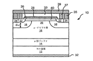
本発明のいくつかの実施形態に基づくIGBT構造が図1に示されている。図1に示されたデバイス10の構造などのプレーナ・デバイス構造は、プロセスの単純化および/またはデバイス信頼性の向上を提供することができる。しかしながら、他のデバイス構造も有利に使用することができる。
An IGBT structure according to some embodiments of the present invention is shown in FIG. Planar device structures, such as the structure of
図1のデバイス10は、n型基板12上に、p型バッファ層14およびp−ドリフト・エピタキシャル層16を含む。基板12は、n+型8°オフアクシス(off−axis)4H−SiC基板を含むことができる。p−ドリフト層16は、約110μmの厚さを有することができ、p−ドリフト層16には、p型ドーパントを、所望のブロッキング電圧を提供するように選択されたドーピング濃度にドープすることができる。例えば、p−ドリフト層16には、ブロッキング能力を10kVにするために、p型ドーパントを、約2×1014cm−3から約6×1014cm−3のドーピング濃度にドープすることができる。p型バッファ層14は、約1μmから約2μmの厚さを有することができ、p型バッファ層14には、p型ドーパントを、約1×1017cm−3のドーピング濃度にドープすることができる。p型バッファ層14は、パンチスルーを防ぐチャネル・ストップ層として提供される。
The
p型ドリフト層16の表面にはn+ウェル領域18が形成される。n+ウェル領域18は、イオン注入によって形成することができ、ドリフト層16内へ約0.5μm延びることができる。
An n +
ドリフト層16上には、エピタキシャルp型チャネル調整層40がある。チャネル調整層40は、約0.1μmから約0.5μmの厚さを有することができ、チャネル調整層40には、約1×1016cm−3から約5×1018cm−3の正味(net)アクセプタ濃度を有するように、p型ドーパントをドープすることができる。具体的には、エピタキシャルp型チャネル調整層40は約0.25μmの厚さを有することができ、アルミニウム・イオンなどのアクセプタ・イオンを、約1×1017cm−3のドーピング濃度にドープすることができる。p型チャネル調整層40が存在することによって、デバイス10のしきい電圧を変更し、かつ/または反転チャネル移動度を向上させることができる。
An epitaxial p-type
デバイス10はさらに、n+コネクタ領域24およびp+エミッタ領域22を含み、これらはそれぞれ、例えば窒素およびアルミニウムの選択注入によって形成することができる。n+コネクタ領域24およびp+エミッタ領域22は、p型チャネル調整層40を貫通してn+ウェル領域18内へ延びる。いくつかの実施形態では、p+エミッタ領域22の底面とn+ウェル領域18の底面との間の距離dを約0.45μm以上とすることができる。距離dを大きくすると、n+ウェル領域18の抵抗をより低くすることができ、その結果、デバイス10のオン状態抵抗を向上させることができる。
The
デバイスの周縁に、ガードリング(gurad−ring)ベースのエッジ端子(図示せず)を提供することができる。他のタイプのエッジ端子を使用してもよい。 A guard-ring based edge terminal (not shown) can be provided at the periphery of the device. Other types of edge terminals may be used.
デバイス10は、隣接するn+ウェル領域18間のドリフト層16内にJFET領域20を含む。隣接するn+ウェル領域18からのJFET抵抗を低減させるために、JFET領域20にp型ドーパントを注入することができる。いくつかの実施形態では、JFET領域20を、エピタキシャル成長プロセスによって形成することができる。
デバイス10はさらにゲート絶縁層26を含み、ゲート絶縁層26は、約400〜1000Åの厚さを有する二酸化シリコンを含むことができる。
The
ゲート絶縁層26上には、例えばポリシリコンのゲート28が形成される。デバイス10のこの表面には層間誘電体層33があり、ゲート28を電気的に絶縁する。
On the
n+コネクタ領域24にはn型オーミック・コンタクト35が形成され、p+エミッタ領域22にはp型オーミック・コンタクト37が形成される。n型オーミック・コンタクト35は、Niおよび/またはNiSiなどのニッケル・ベースの導電層を含むことができる。p型オーミック・コンタクト37は、Alおよび/またはAlSiなどのアルミニウム・ベースの導電層を含むことができる。層間誘電体層33上には金属オーバレイヤ(overlayer)39が形成され、金属オーバレイヤ39は、n型コネクタ領域24とp型エミッタ領域22とを、それらのそれぞれのオーミック・コンタクト35、37を介して電気的に接続する。基板12上には、n型金属コレクタ・オーミック・コンタクト32が形成される。
An n-
図2Aから2Dは、デバイス10の形成中に実行され得るいくつかの操作および形成され得る中間構造10Aから10Dを示す。図2Aを参照すると、n+型8°オフアクシス4H−SiC基板12上に、p型SiCバッファ14およびp−SiCドリフト層16がエピタキシャル成長によって形成される。p型バッファ層14は、約1μmから約2μmの厚さを有することができ、p型バッファ層14には、p型ドーパントを、約1×1017cm−3のドーピング濃度にドープすることができる。p型ドリフト層16の形成後、例えばドリフト層16内への窒素などのドナー・イオンの注入によって、n+ウェル領域18が形成される。n+ウェル領域18を可能な限り深く注入することが望ましいことがある。n+ウェル領域18の深さは、使用可能な注入エネルギーによって制限されることがある。
2A through 2D illustrate some operations that may be performed during the formation of
次いで、注入されたイオンを活性化させるために、この構造を、約1600℃以上の温度でアニールすることができる。具体的には、この構造を、n型ドーパントを活性化させることが当技術分野で知られている標準的なSiC活性化アニール条件でアニールすることができる。 The structure can then be annealed at a temperature of about 1600 ° C. or higher to activate the implanted ions. Specifically, the structure can be annealed with standard SiC activation annealing conditions known in the art to activate n-type dopants.
JFET領域20は例えば、隣接するn+ウェル領域18間のドリフト層16内にアルミニウムを注入することによって形成することができる。隣接するn+ウェル領域18からのJFET抵抗を低減させるために、JFET領域20にp型ドーパントを注入することができる。具体的には、JFETの抵抗を低下させ、同時に注入損傷を許容可能なレベルに維持するように、JFETの注入ドーズを選択することができる。いくつかの実施形態では、このJFET注入を、JFET領域20のドーパント濃度を約1×1016cm−3にするのに十分なドーズで実行することができる。いくつかの実施形態では、このJFET領域を、エピタキシャル成長プロセスによって形成することができる。
The
図2Bを参照すると、ドリフト層16上にエピタキシャル・チャネル調整層40が、例えばよく知られているSiCエピタキシャル再成長技法を使用して形成される。チャネル調整層40には、アクセプタ・イオンを、約1×1017cm−3のドーピング濃度にドープすることができる。
Referring to FIG. 2B, an epitaxial
エピタキシャル・チャネル調整層40は、デバイスのしきい電圧を変更し、かつ/または反転チャネル移動度を向上させることができる。チャネル調整層40はさらに、n型ウェル領域18に比べて浅いp型ソース領域22の形成を可能にすることができる。再成長させたチャネル調整層40の表面の方にp型エミッタ注入22を引き上げることでn型ウェル領域18をより深くすることによって、デバイスのラッチアップを低減させまたは防ぐことができる。n+ウェル18を深くすると、p型エミッタ領域22の底面とn+ウェル18の底面との間の間隔dが大きくなるため、Nウェル抵抗をより低くすることができる。より低いnウェル抵抗は、デバイスのラッチアップ電流を増大させることができ、かつ/またはより良好なオン状態抵抗を提供することができる。
The epitaxial
図2Cを参照すると、例えばエピタキシャル・チャネル調整層40内へ/エピタキシャル・チャネル調整層を貫通してドナー・イオンおよびアクセプタ・イオンを選択注入することによって、それぞれn型コネクタ領域24およびp型エミッタ領域22が形成される。
Referring to FIG. 2C, n-
図2Cに示された距離dは、n型ウェル領域18の垂直方向の長さおよびp型エミッタ領域22の垂直方向の長さの関数であることが理解される。一般に、p型エミッタ領域22の底面とn+ウェル18領域の底面との間の間隔dをできる限り大きくすることが望ましい。さらに、前述のとおり、p型エミッタ領域22は、p型エピタキシャル・チャネル調整層40の形成後に形成することができる。こうして、ウェル領域18の厚さ(深さ)は、デバイスを製造するために使用されるシステムの最大注入エネルギーによって決定される。しかしながら、n型ウェル領域18内へのp+エミッタ領域22の貫入深さは、約0.25μmとすることができるエピタキシャル・チャネル調整層40の厚さの分だけ減少させることができる。
It is understood that the distance d shown in FIG. 2C is a function of the vertical length of the n-
図2Cをさらに参照すると、シリコン加圧下で、かつ/または黒鉛膜などのカプセル層によって覆われた状態で、約1600℃以上の温度でこの構造をアニールすることによって、注入されたドーパントを活性化することができる。いくつかの実施形態では、黒鉛カプセル層を使用し、約1700℃を超える温度でアニールすることによって、注入物を活性化することができる。 With further reference to FIG. 2C, the implanted dopant is activated by annealing the structure at a temperature above about 1600 ° C. under silicon pressure and / or covered by a capsule layer such as a graphite film. can do. In some embodiments, the implant can be activated by using a graphite capsule layer and annealing at a temperature above about 1700 ° C.
高温活性化アニール(例えば1700℃以上)は、しきい値調整イオンの活性化およびチャネル領域40の欠陥のアニールを強化することができる。しかしながら、このような高温アニールは、炭化シリコン・ドリフト層16の表面を傷つける可能性がある。
High-temperature activation annealing (eg, 1700 ° C. or higher) can enhance the activation of threshold adjustment ions and annealing of
図2Cを参照すると、高温アニールの結果生じ得る損傷を低減させるため、ゲート酸化物26、ゲート・コンタクト28およびエミッタ・コンタクト30を形成する前に、構造10Cの表面に黒鉛コーティング50を形成することができる。すなわち、注入されたイオンを活性化するために構造10Cをアニールする前に、構造10Cの上面/表側に、アニールの間、構造の表面を保護する黒鉛コーティング50を堆積させることができる。黒鉛コーティング50は、従来のレジスト・コーティング法によって堆積させることができ、高温アニールの間、下にあるSiC層を保護するのに十分な厚さを有することができる。黒鉛コーティング50は例えば約1μmの厚さを有することができる。チャネル調整層40上に結晶性のコーティングを形成するため、黒鉛コーティング50を加熱することができる。注入されたイオンは、熱アニールによって活性化することができ、この熱アニールは例えば、不活性ガス中で、約1700℃以上の温度で実行することができる。具体的には、この熱アニールを、アルゴン中で、約1850℃の温度で5分間実行することができる。黒鉛コーティング50は、この高温アニールの間、エピタキシャル・チャネル調整層40および/またはドリフト層16の表面を保護するのに役立つことができる。
Referring to FIG. 2C, a
次いで、黒鉛コーティング50を、例えばアッシングおよび熱酸化によって除去することができる。
The
注入物のアニールの後、厚さ約1μmの例えば二酸化シリコンのフィールド酸化物(図示せず)を堆積させ、これをパターン形成して、デバイスの活性領域を露出させることができる。 After annealing the implant, a field oxide (not shown) of about 1 μm thickness, for example silicon dioxide, can be deposited and patterned to expose the active region of the device.
図2Dを参照すると、ゲート酸化プロセスによってゲート絶縁層26を形成することができ、ゲート酸化物の最終的な厚さは400〜600Åとすることができる。
Referring to FIG. 2D, the
ゲート絶縁層26は、黒鉛キャップ層50を除去した後、ドリフト層16の露出した表面に成長させることができる。ゲート絶縁層26は、乾燥O2中でのバルク酸化物の成長と、それに続く湿潤O2中でのバルク酸化物のアニールとを含む乾/湿式酸化プロセスによって成長させた酸化物層を含むことができ、この乾/湿式酸化プロセスは例えば、その開示の全体が参照によって本明細書に組み込まれる米国特許第5,972,801号(特許文献1)に記載されている。本明細書で使用されるとき、湿潤O2中での酸化物のアニールは、O2とH2O蒸気の両方を含む環境での酸化物のアニールを指す。乾式酸化物成長と湿式酸化物成長の間にアニールを実行することができる。乾式O2酸化物成長は、例えば、石英炉管内で、最高約1200℃の温度の乾燥O2中で、少なくとも約2.5時間実行することができる。乾式酸化物成長は、バルク酸化物層を所望の厚さに成長させるために実行される。乾式酸化物成長の温度が酸化物の成長速度に影響を及ぼすことがある。例えば、処理温度が高いほど、酸化物の成長速度は高くなる。最高成長温度は、使用されるシステムによって異なる。乾燥O2成長に関しては、石英管の代わりに例えば炭化ケイ素炉を使用することによって、より高い温度を達成することができる。しかしながら、より高い温度は酸化物の質を向上させない可能性がある。
The
いくつかの実施形態では、この乾式O2酸化物成長を、乾燥O2中で、約1175℃の温度で、約3.5時間実行することができる。その結果生じた酸化物層を、不活性雰囲気で、最高約1200℃の温度でアニールすることができる。具体的には、その結果生じた酸化物層を、Ar中で、約1175℃の温度で、約1時間アニールすることができる。 In some embodiments, this dry O 2 oxide growth can be performed in dry O 2 at a temperature of about 1175 ° C. for about 3.5 hours. The resulting oxide layer can be annealed at temperatures up to about 1200 ° C. in an inert atmosphere. Specifically, the resulting oxide layer can be annealed in Ar at a temperature of about 1175 ° C. for about 1 hour.
湿式O2酸化物アニールは、約950℃以下の温度で、少なくとも約1時間実行することができる。追加の界面状態を導入する可能性があるSiC/SiO2界面でのさらなる熱酸化物成長を防ぐため、湿式O2アニールの温度を制限することができる。具体的には、湿式O2アニールは、湿潤O2中で、約950℃の温度で、約3時間実行することができる。その結果生じるゲート絶縁層26は約500Åの厚さを有することができる。
The wet O 2 oxide anneal may be performed at a temperature of about 950 ° C. or less for at least about 1 hour. In order to prevent further thermal oxide growth at the SiC / SiO 2 interface that could introduce additional interface states, the temperature of the wet O 2 anneal can be limited. Specifically, the wet O 2 anneal can be performed in wet O 2 at a temperature of about 950 ° C. for about 3 hours. The resulting
いくつかの実施形態では、湿式O2アニール・プロセスにおいて使用される水蒸気を、発熱プロセス(pyrogenic process)を使用して発生させることができ、その結果起こる湿式O2アニールを「発熱性酸化(pyrogenic oxidation)」と呼ぶことができる。図3を参照すると、発熱性酸化では、約800℃などの高温に加熱された、アニール室220とは別個の発熱室210内へ、酸素(O2)ガスおよび水素(H2)ガスが流される。水素および酸素ガスは発熱室210内で燃焼し、水蒸気(H2O)と酸素(O2)の混合物を形成し、これがアニール室220に供給される。
In some embodiments, the water vapor used in the wet O 2 anneal process can be generated using a pyrogenic process, and the resulting wet O 2 anneal is “pyrogenic oxidation”. oxidation) ”. Referring to FIG. 3, in the exothermic oxidation, oxygen (O 2 ) gas and hydrogen (H 2 ) gas are flowed into a
いくつかのケースでは、発熱室210内への水素および酸素の流量を、水素と酸素の分子比が2:1に近づくように、しかし2:1を超えないように調整することが望ましいことがある。すなわち、アニール室220に供給される混合物が、合理的な安全限界内において、できるだけ湿っていることが望ましい場合がある。いくつかのケースでは、水素/酸素比1.8:1または1.9:1を使用することができる。
In some cases, it may be desirable to adjust the flow rates of hydrogen and oxygen into the
図2Dを再び参照すると、ゲート絶縁層26の形成後、ポリシリコン・ゲート28を堆積させることができ、ポリシリコン・ゲート28に例えばホウ素をドープすることができ、続いて、ゲート抵抗を低減させるためにメタライゼーション・プロセスを実施することができる。構造10D上に、例えば二酸化シリコンの層間誘電体層33が形成され、層間誘電体層33は、ゲート28および構造10Dの露出部分を覆う。層間誘電体層33にヴィアホールがあけられ、p型エミッタ領域22およびn型コネクタ領域24に達するオーミック・コンタクトが形成される。p型オーミック金属エミッタ・コンタクト37として、Alおよび/またはAlSiなどのAlベースの導電材料を堆積させることができ、n型オーミック金属コンタクト35として、Niおよび/またはNi/SiなどのNiベースの導電層を堆積させることができる。全てのコンタクトを急速熱アニール装置(RTA)内で焼結させることができる。図1に示されているように、p型エミッタ領域22とn型コネクタ領域24とを電気的に接続するために、層間誘電体層上に、厚いTi/Au層などの金属オーバレイヤ39を堆積させることができる。デバイス10の裏面コンタクトとしてn型コレクタ・コンタクト32が形成される。
Referring again to FIG. 2D, after formation of the
アクティブエリアが0.4mm2の前述のプレーナIGBTを製造し、ゲートおよびコレクタに負電位を与えてオン状態およびブロッキング特性を評価した。最大ゲート・バイアスを約−20Vとしたときの0.4mm2IGBTの室温におけるオン状態特性が図4に示されている。ニー電圧は約−3Vであり、エミッタおよびコレクタ上の良好なオーム接触を示している。微分オン抵抗は88mΩ×cm2であり、高電圧IGBTに対して最も低い値である。このようなデバイスの電力損を300W/cm2に設定すると、コレクタ電流密度は約50A/cm2である。この電流密度レベルで、コレクタの電圧降下は約−8.65Vであり、これは、固有オン抵抗約173mΩ×cm2に対応する。 The above-described planar IGBT having an active area of 0.4 mm 2 was manufactured, and a negative potential was applied to the gate and the collector to evaluate the on-state and the blocking characteristics. FIG. 4 shows the on-state characteristics of a 0.4 mm 2 IGBT at room temperature when the maximum gate bias is about −20V. The knee voltage is about -3V, indicating good ohmic contact on the emitter and collector. The differential on-resistance is 88 mΩ × cm 2, which is the lowest value for the high voltage IGBT. If the power loss of such a device is set to 300 W / cm 2 , the collector current density is about 50 A / cm 2 . At this current density level, the collector voltage drop is about −8.65 V, which corresponds to a specific on-resistance of about 173 mΩ × cm 2 .
オン状態において、本発明の実施形態に基づくIGBTは正の温度係数を示すことができる。図5は、同じデバイスの200℃におけるI−V特性を示す。ニー電圧は、−3Vのまま比較的に一定である。微分オン抵抗は、ゲート・バイアス−20Vで約25mΩ×cm2までさらに低下する。コレクタ電流密度50A/cm2において、コレクタの電圧降下は約−5.30Vに低下し、これは、固有オン抵抗約106mΩ×cm2に対応する。高温におけるオン抵抗の低下は、現在使用されているSiC材料内のキャリア寿命が、IGBTオン状態電流伝導能力に関する支配的因子であることを示している可能性がある。10kVクラスのSiC DMOSFETと比較すると、本発明のいくつかの実施形態に基づくIGBTは、おそらくは不十分な抵抗率変調のため、室温においてより高い電圧降下を示す。しかし、高温では、電圧降下が、DMOSFETの値よりも小さくなる。 In the on state, an IGBT according to an embodiment of the present invention can exhibit a positive temperature coefficient. FIG. 5 shows the IV characteristics at 200 ° C. of the same device. The knee voltage remains relatively constant at -3V. The differential on-resistance is further reduced to about 25 mΩ × cm 2 at a gate bias of −20V. At a collector current density of 50 A / cm 2 , the collector voltage drop drops to about −5.30 V, which corresponds to a specific on-resistance of about 106 mΩ × cm 2 . The decrease in on-resistance at high temperatures may indicate that the carrier lifetime in currently used SiC materials is the dominant factor for the IGBT on-state current conduction capability. Compared to a 10 kV class SiC DMOSFET, an IGBT according to some embodiments of the present invention exhibits a higher voltage drop at room temperature, possibly due to insufficient resistivity modulation. However, at high temperatures, the voltage drop is smaller than the value of DMOSFET.
図6は、同じデバイスの室温における電圧ブロッキング特性を示す。具体的には、ゲート電極をエミッタとともに接地し、空気中でのアーク放電を防ぐためFluorinertに浸漬した前述のIGBTデバイスを試験した。図6に示されているように、ゲート・バイアス0Vで、9kVのブロッキング電圧および約0.1mA/cm2未満の漏れ電流密度が達成された。デバイス端子周縁で破壊が起こり、このことは、より良好なエッジ端子設計によって、ドリフト層の厚さによって決定されるブロッキング電圧に近づく余地があることを示している可能性がある。 FIG. 6 shows the voltage blocking characteristics of the same device at room temperature. Specifically, the aforementioned IGBT device immersed in Fluorinert was tested by grounding the gate electrode together with the emitter and preventing arc discharge in the air. As shown in FIG. 6, with a gate bias of 0 V, a blocking voltage of 9 kV and a leakage current density of less than about 0.1 mA / cm 2 were achieved. Breakdown occurs at the periphery of the device terminal, which may indicate that better edge terminal design has room to approach the blocking voltage determined by the drift layer thickness.
IGBTとともに製造された水平4H−SiC p−MOSFETの正孔移動度およびMOSしきい電圧の測定は、このMOSFETデバイスが、室温で約6.5cm2/V−sのピーク・チャネル移動度および約−7.5Vのしきい電圧を有することを示す。このチャネル移動度は、100℃で、最大値約8.2cm2/V−sに達し、しきい電圧は温度とともに低下する。 Measurements of hole mobility and MOS threshold voltage of horizontal 4H-SiC p-MOSFETs fabricated with IGBTs show that this MOSFET device has a peak channel mobility of about 6.5 cm 2 / Vs at room temperature and about It shows having a threshold voltage of -7.5V. This channel mobility reaches a maximum value of about 8.2 cm 2 / V-s at 100 ° C., and the threshold voltage decreases with temperature.
本発明の実施形態に基づくIGBTデバイスでスイッチング試験を実行した。このスイッチング試験には、図7に示されたクランプされた導スイッチング試験回路トポロジ(clamped Inductive Switching Test Circuit topology)を使用した。高い伝導電流を達成するため、このスイッチング試験に使用したIGBTデバイス10のアクティブエリアは4mm2としたが、試験デバイスのそのほかの設計は、前述の設計と同様である。この試験回路では、IGBT10が、フリーホイーリング・ダイオードD1によってクランピングされた1.1mHの誘導負荷L1に結合される。ダイオードD1は、ゼロ逆回復(zero reverse recovery)の2つの直列Cree CSD10120 SiCショットキー・ダイオードを含む。1つのCSD10120ダイオードの定格は1200Vおよび10Aであり、そのため、2つの直列のダイオードは、2400Vのブロッキング能力を提供することができる。キャパシタC1は2μFの静電容量を有し、4kVまでの電圧を取り扱う能力を有する。IGBTをオンにするために、電圧源Vinからの0から−20Vの負パルスを使用した。電源電圧Vssは−500Vである。
A switching test was performed on an IGBT device according to an embodiment of the present invention. For this switching test, the clamped Inductive Switching Test Circuit topology shown in FIG. 7 was used. In order to achieve a high conduction current, the active area of the
図8は、コレクタ電圧−500Vでの25℃におけるスイッチング波形を示す。図8では、水平軸が時間(500ns/目盛)を示し、垂直軸が、ボルト(200V/目盛)および電流(1A/目盛)を示す。立下り時間tfallは、ターンオフにおいて、コレクタ電流が、その2Aであるピークの90%から5%まで低下するのにかかる時間と定義される。立上り時間triseは、ターンオンにおいて、コレクタ電流が、2Aである電流ピークの5%から90%まで上昇するのにかかる時間である。ターンオン遅延時間は、ゲート・バイアス−20が印加されてから、コレクタ電流が2Aピークへ上昇するまでの時間である。ターンオフ遅延時間は、ゲート・バイアスの除去から、コレクタ電流がゼロに向かって低下するまでの時間である。 FIG. 8 shows a switching waveform at 25 ° C. with a collector voltage of −500V. In FIG. 8, the horizontal axis represents time (500 ns / division), and the vertical axis represents volts (200 V / division) and current (1 A / division). Fall time tfall is defined as the time it takes for the collector current to drop from 90% to 5% of its 2A peak at turn-off. The rise time trise is the time it takes for the collector current to rise from 5% to 90% of the current peak at 2A at turn-on. The turn-on delay time is the time from when the gate bias -20 is applied until the collector current rises to the 2A peak. The turn-off delay time is the time from the removal of the gate bias until the collector current decreases toward zero.
表1は、さまざまな温度に対するスイッチング時間を示す。合計スイッチング時間は室温で約350nsであり、200℃では約460nsに増大する。このIGBTは高速スイッチング能力を特徴とし、幅広い温度範囲にわたって高周波数で動作させることができる。合計スイッチング時間の支配的部分はターンオフ遅延時間である可能性があり、これは主に入力キャパシタによって決定される。 Table 1 shows the switching times for various temperatures. The total switching time is about 350 ns at room temperature and increases to about 460 ns at 200 ° C. This IGBT features fast switching capability and can be operated at high frequencies over a wide temperature range. A dominant part of the total switching time may be the turn-off delay time, which is mainly determined by the input capacitor.

本発明のいくつかの実施形態に基づくSiC IGBTsは、高電力および/または高温用途に適する可能性がある。本発明のいくつかの実施形態は、n型4H−SiC基板上の高電圧プレーナIGBTを提供する。いくつかの実施形態では、ゲート・バイアス約−20Vにおいて、25℃で約88mΩ×cm2の微分オン抵抗が達成され、200℃では約24.8mΩ×cm2まで低下する。本発明の実施形態に基づくデバイスは、約9kVのブロッキング電圧および約0.1mA/cm2以下の漏れ電流密度を示すことができる。室温で、正孔チャネル移動度約6.5cm2/V−sおよびしきい電圧−6.5Vが達成され、これらは伝導能力の向上につながる。誘導スイッチング試験は、本発明のいくつかの実施形態に基づくIGBTが、室温と高温の両方で高速スイッチング能力を示すことができることを示した。 SiC IGBTs according to some embodiments of the present invention may be suitable for high power and / or high temperature applications. Some embodiments of the present invention provide a high voltage planar IGBT on an n-type 4H—SiC substrate. In some embodiments, a differential on-resistance of about 88 mΩ × cm 2 is achieved at 25 ° C. at a gate bias of about −20 V and drops to about 24.8 mΩ × cm 2 at 200 ° C. Devices according to embodiments of the invention can exhibit a blocking voltage of about 9 kV and a leakage current density of about 0.1 mA / cm 2 or less. At room temperature, a hole channel mobility of about 6.5 cm 2 / V-s and a threshold voltage of −6.5 V are achieved, which leads to improved conduction capability. Inductive switching tests have shown that IGBTs according to some embodiments of the present invention can exhibit fast switching capability at both room temperature and high temperature.
本発明のいくつかの実施形態に基づくIGBTデバイスは低いオン状態抵抗を示すことができる。具体的には、埋込みチャネルの注入/再成長、熱酸化、注入物の高温活性化、および/または注入物活性化中の黒鉛カプセル封入のうちの1つまたは複数を使用することによって、高いチャネル移動度を達成することができる。本発明のいくつかの実施形態は、高いチャネル密度と低いJFET抵抗との間のより良好なトレードオフを有する最適化されたセル設計を提供することができる。さらに、本発明のいくつかの実施形態は、キャリア注入効率を向上させ、同時に所望のブロッキング能力を維持するように構成されたフィールド・ストッパ層を提供することができる。エピタキシャル・チャネル再成長によって、ならびに/または、高温アニールおよび/もしくは黒鉛カプセル封入を使用したしきい値調整/埋込みチャネル注入物の活性化によって、高いチャネル移動度を得ることができる。高い正孔キャリア濃度を得るために、P型エピタキシャル成長によって、P型エミッタからの高い多数キャリア注入を得ることができる。さらに、本発明のいくつかの実施形態は、nおよびp型材料上の低いオーム接触抵抗を提供することができる。 An IGBT device according to some embodiments of the present invention can exhibit low on-state resistance. Specifically, by using one or more of buried channel implantation / regrowth, thermal oxidation, high temperature activation of the implant, and / or graphite encapsulation during implant activation, Mobility can be achieved. Some embodiments of the present invention can provide an optimized cell design with a better trade-off between high channel density and low JFET resistance. In addition, some embodiments of the present invention can provide a field stopper layer configured to improve carrier injection efficiency while maintaining a desired blocking capability. High channel mobility can be obtained by epitaxial channel regrowth and / or by threshold adjustment / activation of buried channel implants using high temperature annealing and / or graphite encapsulation. To obtain a high hole carrier concentration, high majority carrier injection from the P-type emitter can be obtained by P-type epitaxial growth. Furthermore, some embodiments of the present invention can provide low ohmic contact resistance on n- and p-type materials.
図面および明細書には、本発明の代表的な実施形態が開示されている。特定の用語が使用されるが、それらは、一般的かつ記述的な意味においてのみ使用されており、限定目的では使用されていない。本発明の範囲は以下の特許請求の範囲に記載されている。 In the drawings and specification, there are disclosed exemplary embodiments of the invention. Although specific terms are used, they are used in a general and descriptive sense only and not for limitation purposes. The scope of the invention is set forth in the following claims.
Claims (5)
前記第1の導電型とは反対の第2の導電型を有するドリフト層と、
前記ドリフト層内にあって前記第1の導電型を有するウェル領域と、
前記ドリフト層上にあって前記第2の導電型を有するエピタキシャル・チャネル調整層と、
前記エピタキシャル・チャネル調整層から前記ウェル領域内へ延びるエミッタ領域であって、前記第2の導電型を有し、該エミッタ領域に隣接した前記ウェル領域内にチャネル領域を少なくとも部分的に画定するエミッタ領域と、
前記チャネル領域上のゲート酸化物層と、
前記ゲート酸化物層上のゲートと
前記チャネル調整層から前記ウェル領域内へ延びる前記第1の導電型のコネクタ領域と、
前記コネクタ領域上の第1のオーミック・コンタクトと、
前記エミッタ領域上にあって、前記第1のオーミック・コンタクトとは異なる材料を含む第2のオーミック・コンタクトと、
前記第1のオーミック・コンタクトと前記第2のオーミック・コンタクトとを電気的に接続した金属オーバレイヤと
を含み、
前記第1の導電型はn型であり、前記第2の導電型はp型であり、
前記ドリフト層は前記ウェル領域に隣接したJFET領域を含み、及び、前記エミッタ領域は、前記JFET領域から間隔を置いて配置され、かつ、該エミッタ領域と前記JFET領域との間に前記チャネル領域を画定し、及び、前記JFET領域は前記ドリフト層の残りの部分よりも高いドーパント濃度を有し、
前記チャネル調整層は、0.1μmから0.5μmの厚さ、および1×10 16 cm −3 から5×10 18 cm −3 の正味ドーピング濃度を有する、
絶縁ゲート・バイポーラ・トランジスタ。 A substrate having a first conductivity type;
A drift layer having a second conductivity type opposite to the first conductivity type;
A well region in the drift layer and having the first conductivity type;
An epitaxial channel adjustment layer on the drift layer and having the second conductivity type;
An emitter region extending from the epitaxial channel adjustment layer into the well region, the emitter region having the second conductivity type, and at least partially defining a channel region in the well region adjacent to the emitter region Area,
A gate oxide layer on the channel region;
A gate on the gate oxide layer; and a connector region of the first conductivity type extending from the channel adjustment layer into the well region;
A first ohmic contact on the connector region;
A second ohmic contact on the emitter region and comprising a material different from the first ohmic contact;
A metal overlayer electrically connecting the first ohmic contact and the second ohmic contact;
The first conductivity type is n-type, the second conductivity type is p-type,
The drift layer includes a JFET region adjacent to the well region, and the emitter region is spaced from the JFET region, and the channel region is interposed between the emitter region and the JFET region. defining, and the JFET region have a higher dopant concentration than the remaining portion of the drift layer,
The channel conditioning layer has a thickness of 0.1 μm to 0.5 μm and a net doping concentration of 1 × 10 16 cm −3 to 5 × 10 18 cm −3 ;
Insulated gate bipolar transistor.
p型ドリフト層と、
前記ドリフト層内のn型ウェルと、
前記ドリフト層上のp型チャネル調整層と、
前記チャネル調整層から前記n型ウェル内へ延びるp型エミッタ領域であって、該p型エミッタ領域に隣接した前記n型ウェル内にチャネル領域を少なくとも部分的に画定するp型エミッタ領域と、
前記チャネル調整層から前記n型ウェル内へ延びるn型コネクタ領域と、
前記p型エミッタ領域上の第1のオーミック・コンタクトと、
前記n型コネクタ領域上の第2のオーミック・コンタクトと、
前記チャネル領域上のゲート酸化物層と、
前記ゲート酸化物層上のゲートと、
前記ゲート上にあって、前記第1のオーミック・コンタクトを露出させる第1の開口と、前記第2のオーミック・コンタクトを露出させる第2の開口とを含む層間誘電体層と、
前記層間誘電体層上にあって、前記第1のオーミック・コンタクトと前記第2のオーミック・コンタクトとを電気的に接続する金属オーバレイヤと
を含み、
前記ドリフト層は前記ウェル領域に隣接したJFET領域を含み、及び、前記エミッタ領域は、前記JFET領域から間隔を置いて配置され、かつ、該エミッタ領域と前記JFET領域との間に前記チャネル領域を画定し、及び、前記JFET領域は前記ドリフト層の残りの部分よりも高いドーパント濃度を有し、
前記チャネル調整層は、0.1μmから0.5μmの厚さ、および1×10 16 cm −3 から5×10 18 cm −3 の正味ドーピング濃度を有する、
トランジスタ。 an n-type substrate;
a p-type drift layer;
An n-type well in the drift layer;
A p-type channel adjustment layer on the drift layer;
A p-type emitter region extending from the channel adjustment layer into the n-type well, wherein the p-type emitter region at least partially defines a channel region in the n-type well adjacent to the p-type emitter region;
An n-type connector region extending from the channel adjustment layer into the n-type well;
A first ohmic contact on the p-type emitter region;
A second ohmic contact on the n-type connector region;
A gate oxide layer on the channel region;
A gate on the gate oxide layer;
An interlayer dielectric layer on the gate and including a first opening exposing the first ohmic contact and a second opening exposing the second ohmic contact;
A metal overlayer on the interlayer dielectric layer and electrically connecting the first ohmic contact and the second ohmic contact;
The drift layer includes a JFET region adjacent to the well region, and the emitter region is spaced from the JFET region, and the channel region is interposed between the emitter region and the JFET region. defining, and the JFET region have a higher dopant concentration than the remaining portion of the drift layer,
The channel conditioning layer has a thickness of 0.1 μm to 0.5 μm and a net doping concentration of 1 × 10 16 cm −3 to 5 × 10 18 cm −3 ;
Transistor.
Applications Claiming Priority (3)
| Application Number | Priority Date | Filing Date | Title |
|---|---|---|---|
| US83824906P | 2006-08-17 | 2006-08-17 | |
| US60/838,249 | 2006-08-17 | ||
| PCT/US2007/014139 WO2008020911A2 (en) | 2006-08-17 | 2007-06-18 | High power insulated gate bipolar transistors |
Related Child Applications (1)
| Application Number | Title | Priority Date | Filing Date |
|---|---|---|---|
| JP2013265926A Division JP5771678B2 (en) | 2006-08-17 | 2013-12-24 | High power insulated gate bipolar transistor |
Publications (3)
| Publication Number | Publication Date |
|---|---|
| JP2010521799A JP2010521799A (en) | 2010-06-24 |
| JP2010521799A5 JP2010521799A5 (en) | 2012-08-23 |
| JP5645404B2 true JP5645404B2 (en) | 2014-12-24 |
Family
ID=38896818
Family Applications (2)
| Application Number | Title | Priority Date | Filing Date |
|---|---|---|---|
| JP2009524593A Active JP5645404B2 (en) | 2006-08-17 | 2007-06-18 | High power insulated gate bipolar transistor |
| JP2013265926A Active JP5771678B2 (en) | 2006-08-17 | 2013-12-24 | High power insulated gate bipolar transistor |
Family Applications After (1)
| Application Number | Title | Priority Date | Filing Date |
|---|---|---|---|
| JP2013265926A Active JP5771678B2 (en) | 2006-08-17 | 2013-12-24 | High power insulated gate bipolar transistor |
Country Status (6)
| Country | Link |
|---|---|
| US (2) | US8710510B2 (en) |
| EP (2) | EP2631951B1 (en) |
| JP (2) | JP5645404B2 (en) |
| KR (1) | KR101529331B1 (en) |
| CN (1) | CN101501859B (en) |
| WO (1) | WO2008020911A2 (en) |
Families Citing this family (83)
| Publication number | Priority date | Publication date | Assignee | Title |
|---|---|---|---|---|
| EP2033212B1 (en) * | 2006-06-29 | 2013-10-16 | Cree, Inc. | Method of forming a silicon carbide pmos device |
| US8432012B2 (en) | 2006-08-01 | 2013-04-30 | Cree, Inc. | Semiconductor devices including schottky diodes having overlapping doped regions and methods of fabricating same |
| US7728402B2 (en) | 2006-08-01 | 2010-06-01 | Cree, Inc. | Semiconductor devices including schottky diodes with controlled breakdown |
| JP5645404B2 (en) | 2006-08-17 | 2014-12-24 | クリー インコーポレイテッドCree Inc. | High power insulated gate bipolar transistor |
| US8835987B2 (en) | 2007-02-27 | 2014-09-16 | Cree, Inc. | Insulated gate bipolar transistors including current suppressing layers |
| US7687825B2 (en) * | 2007-09-18 | 2010-03-30 | Cree, Inc. | Insulated gate bipolar conduction transistors (IBCTS) and related methods of fabrication |
| US8043978B2 (en) * | 2007-10-11 | 2011-10-25 | Riken | Electronic device and method for producing electronic device |
| US7989882B2 (en) * | 2007-12-07 | 2011-08-02 | Cree, Inc. | Transistor with A-face conductive channel and trench protecting well region |
| US9640609B2 (en) * | 2008-02-26 | 2017-05-02 | Cree, Inc. | Double guard ring edge termination for silicon carbide devices |
| US8232558B2 (en) | 2008-05-21 | 2012-07-31 | Cree, Inc. | Junction barrier Schottky diodes with current surge capability |
| US8097919B2 (en) | 2008-08-11 | 2012-01-17 | Cree, Inc. | Mesa termination structures for power semiconductor devices including mesa step buffers |
| US8288220B2 (en) * | 2009-03-27 | 2012-10-16 | Cree, Inc. | Methods of forming semiconductor devices including epitaxial layers and related structures |
| CN102396069B (en) * | 2009-04-16 | 2014-05-07 | 三菱电机株式会社 | Method for manufacturing silicon carbide Schottky diode |
| US8294507B2 (en) | 2009-05-08 | 2012-10-23 | Cree, Inc. | Wide bandgap bipolar turn-off thyristor having non-negative temperature coefficient and related control circuits |
| US8637386B2 (en) | 2009-05-12 | 2014-01-28 | Cree, Inc. | Diffused junction termination structures for silicon carbide devices and methods of fabricating silicon carbide devices incorporating same |
| US8629509B2 (en) * | 2009-06-02 | 2014-01-14 | Cree, Inc. | High voltage insulated gate bipolar transistors with minority carrier diverter |
| US8193848B2 (en) | 2009-06-02 | 2012-06-05 | Cree, Inc. | Power switching devices having controllable surge current capabilities |
| US8541787B2 (en) * | 2009-07-15 | 2013-09-24 | Cree, Inc. | High breakdown voltage wide band-gap MOS-gated bipolar junction transistors with avalanche capability |
| US8314462B2 (en) * | 2009-07-28 | 2012-11-20 | Cree, Inc. | Semiconductor devices including electrodes with integrated resistances |
| US8354690B2 (en) | 2009-08-31 | 2013-01-15 | Cree, Inc. | Solid-state pinch off thyristor circuits |
| US8563986B2 (en) * | 2009-11-03 | 2013-10-22 | Cree, Inc. | Power semiconductor devices having selectively doped JFET regions and related methods of forming such devices |
| US9117739B2 (en) | 2010-03-08 | 2015-08-25 | Cree, Inc. | Semiconductor devices with heterojunction barrier regions and methods of fabricating same |
| US8415671B2 (en) | 2010-04-16 | 2013-04-09 | Cree, Inc. | Wide band-gap MOSFETs having a heterojunction under gate trenches thereof and related methods of forming such devices |
| CN102473726B (en) * | 2010-05-27 | 2014-08-27 | 松下电器产业株式会社 | Semiconductor device and method for driving same |
| CN102263127B (en) * | 2010-05-29 | 2013-06-19 | 比亚迪股份有限公司 | MOS (Metal Oxide Semiconductor) type power device and manufacturing method thereof |
| JP2011253883A (en) * | 2010-06-01 | 2011-12-15 | On Semiconductor Trading Ltd | Semiconductor device and manufacturing method of the same |
| GB2484506A (en) * | 2010-10-13 | 2012-04-18 | Univ Warwick | Heterogrowth |
| WO2012063310A1 (en) * | 2010-11-08 | 2012-05-18 | 株式会社日立製作所 | Semiconductor device |
| US8803277B2 (en) | 2011-02-10 | 2014-08-12 | Cree, Inc. | Junction termination structures including guard ring extensions and methods of fabricating electronic devices incorporating same |
| CN102760759B (en) * | 2011-04-29 | 2016-02-03 | 比亚迪股份有限公司 | A kind of semiconductor power device |
| US9142662B2 (en) | 2011-05-06 | 2015-09-22 | Cree, Inc. | Field effect transistor devices with low source resistance |
| US9029945B2 (en) | 2011-05-06 | 2015-05-12 | Cree, Inc. | Field effect transistor devices with low source resistance |
| US9171977B2 (en) * | 2011-06-17 | 2015-10-27 | Cree, Inc. | Optically assist-triggered wide bandgap thyristors having positive temperature coefficients |
| CN102244099B (en) * | 2011-06-23 | 2013-04-17 | 西安电子科技大学 | SiC IEMOSFET (Implantation and Epitaxial Metal-Oxide -Semiconductor Field Effect Transistor) device with epitaxy channel and manufacturing method of SiC IEMOSFET device |
| US8664665B2 (en) | 2011-09-11 | 2014-03-04 | Cree, Inc. | Schottky diode employing recesses for elements of junction barrier array |
| US9640617B2 (en) | 2011-09-11 | 2017-05-02 | Cree, Inc. | High performance power module |
| US8680587B2 (en) | 2011-09-11 | 2014-03-25 | Cree, Inc. | Schottky diode |
| EP2754177A1 (en) | 2011-09-11 | 2014-07-16 | Cree, Inc. | High current density power module comprising transistors with improved layout |
| US9373617B2 (en) | 2011-09-11 | 2016-06-21 | Cree, Inc. | High current, low switching loss SiC power module |
| US8618582B2 (en) | 2011-09-11 | 2013-12-31 | Cree, Inc. | Edge termination structure employing recesses for edge termination elements |
| GB2495949B (en) * | 2011-10-26 | 2015-03-11 | Anvil Semiconductors Ltd | Silicon carbide epitaxy |
| CN103151262A (en) * | 2011-12-07 | 2013-06-12 | 无锡华润华晶微电子有限公司 | Planar insulated gate bipolar transistor and preparation method thereof |
| JP5611184B2 (en) * | 2011-12-14 | 2014-10-22 | 三菱電機株式会社 | Heat treatment method in the manufacture of semiconductor devices |
| JP2013258333A (en) * | 2012-06-13 | 2013-12-26 | Toshiba Corp | Power semiconductor device |
| US9054183B2 (en) * | 2012-07-13 | 2015-06-09 | United Silicon Carbide, Inc. | Trenched and implanted accumulation mode metal-oxide-semiconductor field-effect transistor |
| JP6264768B2 (en) * | 2012-07-31 | 2018-01-24 | 国立研究開発法人産業技術総合研究所 | Semiconductor structure, semiconductor device, and method of manufacturing the semiconductor structure |
| US10094988B2 (en) * | 2012-08-31 | 2018-10-09 | Micron Technology, Inc. | Method of forming photonics structures |
| CN103973960B (en) * | 2013-02-01 | 2017-05-24 | 华晶科技股份有限公司 | Camera device and focusing method |
| US9240476B2 (en) | 2013-03-13 | 2016-01-19 | Cree, Inc. | Field effect transistor devices with buried well regions and epitaxial layers |
| US9306061B2 (en) * | 2013-03-13 | 2016-04-05 | Cree, Inc. | Field effect transistor devices with protective regions |
| US9012984B2 (en) | 2013-03-13 | 2015-04-21 | Cree, Inc. | Field effect transistor devices with regrown p-layers |
| US9142668B2 (en) | 2013-03-13 | 2015-09-22 | Cree, Inc. | Field effect transistor devices with buried well protection regions |
| JP6189131B2 (en) * | 2013-08-01 | 2017-08-30 | 株式会社東芝 | Semiconductor device and manufacturing method thereof |
| US9331197B2 (en) | 2013-08-08 | 2016-05-03 | Cree, Inc. | Vertical power transistor device |
| US10868169B2 (en) * | 2013-09-20 | 2020-12-15 | Cree, Inc. | Monolithically integrated vertical power transistor and bypass diode |
| US9214572B2 (en) * | 2013-09-20 | 2015-12-15 | Monolith Semiconductor Inc. | High voltage MOSFET devices and methods of making the devices |
| WO2015048445A1 (en) * | 2013-09-27 | 2015-04-02 | The Government Of The United States Of America, As Represented By The Secretary Of The Navy | Elimination of basal plane dislocations in post growth silicon carbide epitaxial layers by high temperature annealing while preserving surface morphology |
| CN104517837B (en) * | 2013-09-29 | 2017-10-10 | 无锡华润上华科技有限公司 | A kind of manufacture method of insulated gate bipolar transistor |
| US9111919B2 (en) * | 2013-10-03 | 2015-08-18 | Cree, Inc. | Field effect device with enhanced gate dielectric structure |
| JP6119577B2 (en) | 2013-11-26 | 2017-04-26 | 三菱電機株式会社 | Semiconductor device |
| US9318587B2 (en) | 2014-05-30 | 2016-04-19 | Alpha And Omega Semiconductor Incorporated | Injection control in semiconductor power devices |
| JP6425950B2 (en) * | 2014-09-12 | 2018-11-21 | 株式会社Screenホールディングス | Semiconductor manufacturing method and semiconductor manufacturing apparatus |
| CN104282766A (en) * | 2014-11-06 | 2015-01-14 | 株洲南车时代电气股份有限公司 | Novel silicon carbide MOSFET and manufacturing method thereof |
| CN104319292A (en) * | 2014-11-06 | 2015-01-28 | 株洲南车时代电气股份有限公司 | Novel silicon carbide MOSFET and manufacturing method thereof |
| JP2016127177A (en) * | 2015-01-06 | 2016-07-11 | 住友電気工業株式会社 | Silicon carbide substrate, silicon carbide semiconductor device and silicon carbide substrate manufacturing method |
| KR101692000B1 (en) * | 2015-01-08 | 2017-01-09 | 메이플세미컨덕터(주) | Manufacturing Methods of Thermal Oxide Layer For SiC Power Semiconductor Devices And Manufacturing Methods of SiC Power Semiconductor Devices |
| CN104966735A (en) * | 2015-05-26 | 2015-10-07 | 株洲南车时代电气股份有限公司 | Silicon carbide MOSFET device and preparation method thereof |
| JP6706786B2 (en) * | 2015-10-30 | 2020-06-10 | 一般財団法人電力中央研究所 | Epitaxial wafer manufacturing method, epitaxial wafer, semiconductor device manufacturing method, and semiconductor device |
| JP6657963B2 (en) * | 2016-01-05 | 2020-03-04 | 富士電機株式会社 | MOSFET |
| JP6544252B2 (en) * | 2016-01-26 | 2019-07-17 | 豊田合成株式会社 | Semiconductor device, power conversion device, and method of manufacturing semiconductor device |
| JP6711100B2 (en) * | 2016-04-15 | 2020-06-17 | 富士電機株式会社 | Silicon carbide semiconductor device, method for manufacturing silicon carbide semiconductor device, and method for controlling silicon carbide semiconductor device |
| CN106024627A (en) * | 2016-07-22 | 2016-10-12 | 泰科天润半导体科技(北京)有限公司 | Manufacturing method of SiC-based super-junction IGBT (Insulated Gate Bipolar Transistor) with low off-state loss |
| CN107785365B (en) * | 2016-08-31 | 2021-08-06 | 无锡华润上华科技有限公司 | Device with integrated junction field effect transistor and method of making the same |
| DE102019117897B4 (en) * | 2018-09-28 | 2024-03-21 | Taiwan Semiconductor Manufacturing Co., Ltd. | SEMICONDUCTOR DEVICE FOR LOGIC AND MEMORY CO-OPTIMIZATION AND CIRCUIT |
| US10763863B2 (en) | 2018-09-28 | 2020-09-01 | Taiwan Semiconductor Manufacturing Co., Ltd. | Semiconductor device for logic and memory co-optimization |
| US20200105874A1 (en) | 2018-10-01 | 2020-04-02 | Ipower Semiconductor | Back side dopant activation in field stop igbt |
| JP7189848B2 (en) * | 2019-08-07 | 2022-12-14 | 株式会社東芝 | Semiconductor device and its manufacturing method |
| KR102251761B1 (en) * | 2019-11-27 | 2021-05-14 | 현대모비스 주식회사 | Power semiconductor device |
| CN111682063B (en) * | 2020-05-22 | 2022-05-13 | 东莞市天域半导体科技有限公司 | Ultrahigh-voltage P-channel SiC-IGBT device material and manufacturing method thereof |
| JP2022049822A (en) | 2020-09-17 | 2022-03-30 | キオクシア株式会社 | Semiconductor storage device |
| CN112750807B (en) * | 2021-02-26 | 2022-09-09 | 东莞市中之电子科技有限公司 | A MOSFET tube with shielding buffer structure |
| CN113284954B (en) * | 2021-07-22 | 2021-09-24 | 成都蓉矽半导体有限公司 | A kind of high channel density silicon carbide MOSFET and preparation method thereof |
| US12237407B2 (en) | 2022-11-01 | 2025-02-25 | Globalfoundries U.S. Inc. | Heterojunction bipolar transistor with amorphous semiconductor regions |
Family Cites Families (254)
| Publication number | Priority date | Publication date | Assignee | Title |
|---|---|---|---|---|
| US3439189A (en) | 1965-12-28 | 1969-04-15 | Teletype Corp | Gated switching circuit comprising parallel combination of latching and shunt switches series-connected with input-output control means |
| US3629011A (en) | 1967-09-11 | 1971-12-21 | Matsushita Electric Ind Co Ltd | Method for diffusing an impurity substance into silicon carbide |
| US3924024A (en) | 1973-04-02 | 1975-12-02 | Ncr Co | Process for fabricating MNOS non-volatile memories |
| FR2347780A1 (en) | 1976-07-21 | 1977-11-04 | Bicosa Recherches | IMPROVEMENTS MADE TO A BISTABLE ELEMENT AND SWITCH CIRCUIT CONTAINING SUCH A BISTABLE ELEMENT |
| US4242690A (en) | 1978-06-06 | 1980-12-30 | General Electric Company | High breakdown voltage semiconductor device |
| US4466172A (en) | 1979-01-08 | 1984-08-21 | American Microsystems, Inc. | Method for fabricating MOS device with self-aligned contacts |
| US4581542A (en) | 1983-11-14 | 1986-04-08 | General Electric Company | Driver circuits for emitter switch gate turn-off SCR devices |
| US4644637A (en) | 1983-12-30 | 1987-02-24 | General Electric Company | Method of making an insulated-gate semiconductor device with improved shorting region |
| JPS60177266U (en) | 1984-05-02 | 1985-11-25 | 株式会社 大井製作所 | door check device |
| JPS60240158A (en) | 1984-05-14 | 1985-11-29 | Mitsubishi Electric Corp | semiconductor circuit |
| DE3581348D1 (en) | 1984-09-28 | 1991-02-21 | Siemens Ag | METHOD FOR PRODUCING A PN TRANSITION WITH A HIGH BREAKTHROUGH VOLTAGE. |
| US4811065A (en) | 1987-06-11 | 1989-03-07 | Siliconix Incorporated | Power DMOS transistor with high speed body diode |
| JPS6449273A (en) | 1987-08-19 | 1989-02-23 | Mitsubishi Electric Corp | Semiconductor device and its manufacture |
| JPH0734470B2 (en) * | 1987-09-24 | 1995-04-12 | 三菱電機株式会社 | Field effect semiconductor device |
| US4875083A (en) | 1987-10-26 | 1989-10-17 | North Carolina State University | Metal-insulator-semiconductor capacitor formed on silicon carbide |
| US4866005A (en) | 1987-10-26 | 1989-09-12 | North Carolina State University | Sublimation of silicon carbide to produce large, device quality single crystals of silicon carbide |
| US5011549A (en) | 1987-10-26 | 1991-04-30 | North Carolina State University | Homoepitaxial growth of Alpha-SiC thin films and semiconductor devices fabricated thereon |
| US4945394A (en) | 1987-10-26 | 1990-07-31 | North Carolina State University | Bipolar junction transistor on silicon carbide |
| JPH0614763Y2 (en) | 1988-01-29 | 1994-04-20 | 一雄 上田 | Evacuation equipment |
| JP2843037B2 (en) * | 1988-09-20 | 1999-01-06 | 株式会社日立製作所 | Method for manufacturing semiconductor device |
| JP2680083B2 (en) | 1988-12-06 | 1997-11-19 | 富士通株式会社 | Semiconductor substrate and method of manufacturing the same |
| JPH02275675A (en) | 1988-12-29 | 1990-11-09 | Fuji Electric Co Ltd | MOS type semiconductor device |
| DE59010606D1 (en) | 1989-03-29 | 1997-01-30 | Siemens Ag | Process for the production of a planar pn junction with high dielectric strength |
| US5111253A (en) | 1989-05-09 | 1992-05-05 | General Electric Company | Multicellular FET having a Schottky diode merged therewith |
| US4927772A (en) | 1989-05-30 | 1990-05-22 | General Electric Company | Method of making high breakdown voltage semiconductor device |
| JPH0766971B2 (en) | 1989-06-07 | 1995-07-19 | シャープ株式会社 | Silicon carbide semiconductor device |
| US5028977A (en) | 1989-06-16 | 1991-07-02 | Massachusetts Institute Of Technology | Merged bipolar and insulated gate transistors |
| JP2623850B2 (en) | 1989-08-25 | 1997-06-25 | 富士電機株式会社 | Conductivity modulation type MOSFET |
| US4946547A (en) | 1989-10-13 | 1990-08-07 | Cree Research, Inc. | Method of preparing silicon carbide surfaces for crystal growth |
| JPH03157974A (en) | 1989-11-15 | 1991-07-05 | Nec Corp | vertical field effect transistor |
| JPH03225870A (en) | 1990-01-31 | 1991-10-04 | Toshiba Corp | Manufacture of heterojunction bipolar transistor |
| US5210051A (en) | 1990-03-27 | 1993-05-11 | Cree Research, Inc. | High efficiency light emitting diodes from bipolar gallium nitride |
| JP2542448B2 (en) | 1990-05-24 | 1996-10-09 | シャープ株式会社 | Field effect transistor and method of manufacturing the same |
| US5292501A (en) | 1990-06-25 | 1994-03-08 | Degenhardt Charles R | Use of a carboxy-substituted polymer to inhibit plaque formation without tooth staining |
| US5200022A (en) | 1990-10-03 | 1993-04-06 | Cree Research, Inc. | Method of improving mechanically prepared substrate surfaces of alpha silicon carbide for deposition of beta silicon carbide thereon and resulting product |
| US5192987A (en) | 1991-05-17 | 1993-03-09 | Apa Optics, Inc. | High electron mobility transistor with GaN/Alx Ga1-x N heterojunctions |
| US5270554A (en) | 1991-06-14 | 1993-12-14 | Cree Research, Inc. | High power high frequency metal-semiconductor field-effect transistor formed in silicon carbide |
| US5155289A (en) | 1991-07-01 | 1992-10-13 | General Atomics | High-voltage solid-state switching devices |
| JPH0529628A (en) * | 1991-07-19 | 1993-02-05 | Fuji Electric Co Ltd | Insulated gate bipolar transistor |
| US5170455A (en) | 1991-10-30 | 1992-12-08 | At&T Bell Laboratories | Optical connective device |
| US5242841A (en) | 1992-03-25 | 1993-09-07 | Texas Instruments Incorporated | Method of making LDMOS transistor with self-aligned source/backgate and photo-aligned gate |
| US5459107A (en) | 1992-06-05 | 1995-10-17 | Cree Research, Inc. | Method of obtaining high quality silicon dioxide passivation on silicon carbide and resulting passivated structures |
| US6344663B1 (en) | 1992-06-05 | 2002-02-05 | Cree, Inc. | Silicon carbide CMOS devices |
| US5612260A (en) | 1992-06-05 | 1997-03-18 | Cree Research, Inc. | Method of obtaining high quality silicon dioxide passivation on silicon carbide and resulting passivated structures |
| US5726463A (en) | 1992-08-07 | 1998-03-10 | General Electric Company | Silicon carbide MOSFET having self-aligned gate structure |
| US5587870A (en) | 1992-09-17 | 1996-12-24 | Research Foundation Of State University Of New York | Nanocrystalline layer thin film capacitors |
| JP3146694B2 (en) | 1992-11-12 | 2001-03-19 | 富士電機株式会社 | Silicon carbide MOSFET and method of manufacturing silicon carbide MOSFET |
| US5506421A (en) | 1992-11-24 | 1996-04-09 | Cree Research, Inc. | Power MOSFET in silicon carbide |
| KR100305123B1 (en) | 1992-12-11 | 2001-11-22 | 비센트 비.인그라시아, 알크 엠 아헨 | Static Random Access Memory Cells and Semiconductor Devices Containing These |
| JPH0799312A (en) | 1993-02-22 | 1995-04-11 | Texas Instr Inc <Ti> | Semiconductor device and its manufacturing method |
| JP2811526B2 (en) | 1993-04-19 | 1998-10-15 | 東洋電機製造株式会社 | Static induction semiconductor device with static induction Schottky short circuit |
| US5371383A (en) * | 1993-05-14 | 1994-12-06 | Kobe Steel Usa Inc. | Highly oriented diamond film field-effect transistor |
| JP3310386B2 (en) * | 1993-05-25 | 2002-08-05 | 忠弘 大見 | Method of forming insulating oxide film and semiconductor device |
| US5539217A (en) | 1993-08-09 | 1996-07-23 | Cree Research, Inc. | Silicon carbide thyristor |
| US5479316A (en) | 1993-08-24 | 1995-12-26 | Analog Devices, Inc. | Integrated circuit metal-oxide-metal capacitor and method of making same |
| US5510630A (en) | 1993-10-18 | 1996-04-23 | Westinghouse Electric Corporation | Non-volatile random access memory cell constructed of silicon carbide |
| US5393993A (en) | 1993-12-13 | 1995-02-28 | Cree Research, Inc. | Buffer structure between silicon carbide and gallium nitride and resulting semiconductor devices |
| US5396085A (en) | 1993-12-28 | 1995-03-07 | North Carolina State University | Silicon carbide switching device with rectifying-gate |
| US5385855A (en) | 1994-02-24 | 1995-01-31 | General Electric Company | Fabrication of silicon carbide integrated circuits |
| US5488236A (en) | 1994-05-26 | 1996-01-30 | North Carolina State University | Latch-up resistant bipolar transistor with trench IGFET and buried collector |
| CN1040814C (en) | 1994-07-20 | 1998-11-18 | 电子科技大学 | A surface withstand voltage region for semiconductor devices |
| TW286435B (en) * | 1994-07-27 | 1996-09-21 | Siemens Ag | |
| US5523589A (en) | 1994-09-20 | 1996-06-04 | Cree Research, Inc. | Vertical geometry light emitting diode with group III nitride active layer and extended lifetime |
| JPH08213607A (en) | 1995-02-08 | 1996-08-20 | Ngk Insulators Ltd | Semiconductor device and manufacturing method thereof |
| US5510281A (en) | 1995-03-20 | 1996-04-23 | General Electric Company | Method of fabricating a self-aligned DMOS transistor device using SiC and spacers |
| JP3521246B2 (en) | 1995-03-27 | 2004-04-19 | 沖電気工業株式会社 | Field effect transistor and method of manufacturing the same |
| DE69512021T2 (en) | 1995-03-31 | 2000-05-04 | Consorzio Per La Ricerca Sulla Microelettronica Nel Mezzogiorno, Catania | DMOS array structure and method of manufacture |
| SE9501310D0 (en) | 1995-04-10 | 1995-04-10 | Abb Research Ltd | A method for introducing an impurity dopant into SiC, a semiconductor device formed by the method and using a highly doped amorphous layer as a source for dopant diffusion into SiC |
| US5734180A (en) | 1995-06-02 | 1998-03-31 | Texas Instruments Incorporated | High-performance high-voltage device structures |
| US6693310B1 (en) | 1995-07-19 | 2004-02-17 | Mitsubishi Denki Kabushiki Kaisha | Semiconductor device and manufacturing method thereof |
| US5967795A (en) | 1995-08-30 | 1999-10-19 | Asea Brown Boveri Ab | SiC semiconductor device comprising a pn junction with a voltage absorbing edge |
| FR2738394B1 (en) | 1995-09-06 | 1998-06-26 | Nippon Denso Co | SILICON CARBIDE SEMICONDUCTOR DEVICE, AND MANUFACTURING METHOD THEREOF |
| US6573534B1 (en) * | 1995-09-06 | 2003-06-03 | Denso Corporation | Silicon carbide semiconductor device |
| JPH11261061A (en) | 1998-03-11 | 1999-09-24 | Denso Corp | Silicon carbide semiconductor device and method of manufacturing the same |
| JP4001960B2 (en) | 1995-11-03 | 2007-10-31 | フリースケール セミコンダクター インコーポレイテッド | Method for manufacturing a semiconductor device having a nitrided oxide dielectric layer |
| US5972801A (en) * | 1995-11-08 | 1999-10-26 | Cree Research, Inc. | Process for reducing defects in oxide layers on silicon carbide |
| US6136728A (en) | 1996-01-05 | 2000-10-24 | Yale University | Water vapor annealing process |
| US6133587A (en) | 1996-01-23 | 2000-10-17 | Denso Corporation | Silicon carbide semiconductor device and process for manufacturing same |
| JPH09205202A (en) | 1996-01-26 | 1997-08-05 | Matsushita Electric Works Ltd | Semiconductor device |
| JPH09232332A (en) * | 1996-02-27 | 1997-09-05 | Fuji Electric Co Ltd | Semiconductor device |
| SE9601174D0 (en) | 1996-03-27 | 1996-03-27 | Abb Research Ltd | A method for producing a semiconductor device having a semiconductor layer of SiC and such a device |
| US5877045A (en) | 1996-04-10 | 1999-03-02 | Lsi Logic Corporation | Method of forming a planar surface during multi-layer interconnect formation by a laser-assisted dielectric deposition |
| US5719409A (en) | 1996-06-06 | 1998-02-17 | Cree Research, Inc. | Silicon carbide metal-insulator semiconductor field effect transistor |
| US5763905A (en) | 1996-07-09 | 1998-06-09 | Abb Research Ltd. | Semiconductor device having a passivation layer |
| SE9602745D0 (en) | 1996-07-11 | 1996-07-11 | Abb Research Ltd | A method for producing a channel region layer in a SiC layer for a voltage controlled semiconductor device |
| US6002159A (en) | 1996-07-16 | 1999-12-14 | Abb Research Ltd. | SiC semiconductor device comprising a pn junction with a voltage absorbing edge |
| US5917203A (en) | 1996-07-29 | 1999-06-29 | Motorola, Inc. | Lateral gate vertical drift region transistor |
| SE9602993D0 (en) | 1996-08-16 | 1996-08-16 | Abb Research Ltd | A bipolar semiconductor device having semiconductor layers of SiC and a method for producing a semiconductor device of SiC |
| US5939763A (en) | 1996-09-05 | 1999-08-17 | Advanced Micro Devices, Inc. | Ultrathin oxynitride structure and process for VLSI applications |
| EP1895595B8 (en) | 1996-10-18 | 2013-11-06 | Hitachi, Ltd. | Semiconductor device and electric power conversion apparatus therewith |
| US6028012A (en) | 1996-12-04 | 2000-02-22 | Yale University | Process for forming a gate-quality insulating layer on a silicon carbide substrate |
| JP3225870B2 (en) | 1996-12-05 | 2001-11-05 | トヨタ車体株式会社 | Roof spoiler mounting structure |
| US5837572A (en) | 1997-01-10 | 1998-11-17 | Advanced Micro Devices, Inc. | CMOS integrated circuit formed by using removable spacers to produce asymmetrical NMOS junctions before asymmetrical PMOS junctions for optimizing thermal diffusivity of dopants implanted therein |
| SE9700141D0 (en) | 1997-01-20 | 1997-01-20 | Abb Research Ltd | A schottky diode of SiC and a method of production thereof |
| SE9700156D0 (en) | 1997-01-21 | 1997-01-21 | Abb Research Ltd | Junction termination for Si C Schottky diode |
| US6180958B1 (en) | 1997-02-07 | 2001-01-30 | James Albert Cooper, Jr. | Structure for increasing the maximum voltage of silicon carbide power transistors |
| JP3206727B2 (en) | 1997-02-20 | 2001-09-10 | 富士電機株式会社 | Silicon carbide vertical MOSFET and method of manufacturing the same |
| DE19809554B4 (en) | 1997-03-05 | 2008-04-03 | Denso Corp., Kariya | silicon carbide semiconductor device |
| EP0865085A1 (en) | 1997-03-11 | 1998-09-16 | STMicroelectronics S.r.l. | Insulated gate bipolar transistor with high dynamic ruggedness |
| JPH10284718A (en) | 1997-04-08 | 1998-10-23 | Fuji Electric Co Ltd | Insulated gate type thyristor |
| US6121633A (en) | 1997-06-12 | 2000-09-19 | Cree Research, Inc. | Latch-up free power MOS-bipolar transistor |
| US5969378A (en) | 1997-06-12 | 1999-10-19 | Cree Research, Inc. | Latch-up free power UMOS-bipolar transistor |
| US6063698A (en) | 1997-06-30 | 2000-05-16 | Motorola, Inc. | Method for manufacturing a high dielectric constant gate oxide for use in semiconductor integrated circuits |
| US5877041A (en) | 1997-06-30 | 1999-03-02 | Harris Corporation | Self-aligned power field effect transistor in silicon carbide |
| DE19832329A1 (en) | 1997-07-31 | 1999-02-04 | Siemens Ag | Silicon carbide semiconductor structure manufacturing method |
| JP3180895B2 (en) | 1997-08-18 | 2001-06-25 | 富士電機株式会社 | Method for manufacturing silicon carbide semiconductor device |
| CN1267397A (en) | 1997-08-20 | 2000-09-20 | 西门子公司 | Semiconductor structure comprising alpha silicon carbide zone, and use of said semiconductor structure |
| US6239463B1 (en) | 1997-08-28 | 2001-05-29 | Siliconix Incorporated | Low resistance power MOSFET or other device containing silicon-germanium layer |
| WO1999013512A1 (en) | 1997-09-10 | 1999-03-18 | Infineon Technologies Ag | Semiconductor component with a drift zone |
| SE9704150D0 (en) | 1997-11-13 | 1997-11-13 | Abb Research Ltd | Semiconductor device of SiC with insulating layer a refractory metal nitride layer |
| JP3085272B2 (en) * | 1997-12-19 | 2000-09-04 | 富士電機株式会社 | Method for forming thermal oxide film on silicon carbide semiconductor device |
| JPH11191559A (en) | 1997-12-26 | 1999-07-13 | Matsushita Electric Works Ltd | Method of manufacturing MOSFET |
| JPH11251592A (en) | 1998-01-05 | 1999-09-17 | Denso Corp | Silicon carbide semiconductor device |
| JP3216804B2 (en) | 1998-01-06 | 2001-10-09 | 富士電機株式会社 | Manufacturing method of silicon carbide vertical FET and silicon carbide vertical FET |
| JPH11266017A (en) | 1998-01-14 | 1999-09-28 | Denso Corp | Silicon carbide semiconductor device and method of manufacturing the same |
| JPH11238742A (en) | 1998-02-23 | 1999-08-31 | Denso Corp | Method for manufacturing silicon carbide semiconductor device |
| JP3893725B2 (en) | 1998-03-25 | 2007-03-14 | 株式会社デンソー | Method for manufacturing silicon carbide semiconductor device |
| JPH11330468A (en) * | 1998-05-20 | 1999-11-30 | Hitachi Ltd | Method of manufacturing semiconductor integrated circuit device and semiconductor integrated circuit device |
| US6627539B1 (en) | 1998-05-29 | 2003-09-30 | Newport Fab, Llc | Method of forming dual-damascene interconnect structures employing low-k dielectric materials |
| US6303410B1 (en) * | 1998-06-01 | 2001-10-16 | North Carolina State University | Methods of forming power semiconductor devices having T-shaped gate electrodes |
| US6107142A (en) | 1998-06-08 | 2000-08-22 | Cree Research, Inc. | Self-aligned methods of fabricating silicon carbide power devices by implantation and lateral diffusion |
| US6100169A (en) | 1998-06-08 | 2000-08-08 | Cree, Inc. | Methods of fabricating silicon carbide power devices by controlled annealing |
| US6316793B1 (en) | 1998-06-12 | 2001-11-13 | Cree, Inc. | Nitride based transistors on semi-insulating silicon carbide substrates |
| US5960289A (en) | 1998-06-22 | 1999-09-28 | Motorola, Inc. | Method for making a dual-thickness gate oxide layer using a nitride/oxide composite region |
| JP4003296B2 (en) | 1998-06-22 | 2007-11-07 | 株式会社デンソー | Silicon carbide semiconductor device and manufacturing method thereof |
| JP4123636B2 (en) | 1998-06-22 | 2008-07-23 | 株式会社デンソー | Silicon carbide semiconductor device and manufacturing method thereof |
| US6221700B1 (en) | 1998-07-31 | 2001-04-24 | Denso Corporation | Method of manufacturing silicon carbide semiconductor device with high activation rate of impurities |
| JP2000106371A (en) | 1998-07-31 | 2000-04-11 | Denso Corp | Method for manufacturing silicon carbide semiconductor device |
| JP3959856B2 (en) | 1998-07-31 | 2007-08-15 | 株式会社デンソー | Silicon carbide semiconductor device and manufacturing method thereof |
| US6972436B2 (en) | 1998-08-28 | 2005-12-06 | Cree, Inc. | High voltage, high temperature capacitor and interconnection structures |
| US6246076B1 (en) | 1998-08-28 | 2001-06-12 | Cree, Inc. | Layered dielectric on silicon carbide semiconductor structures |
| SE9802909L (en) | 1998-08-31 | 1999-10-13 | Abb Research Ltd | Method for preparing a pn junction for a SiC semiconductor device and a SiC semiconductor pn junction device |
| EP1001459B1 (en) | 1998-09-09 | 2011-11-09 | Texas Instruments Incorporated | Integrated circuit comprising a capacitor and method |
| JP4186337B2 (en) | 1998-09-30 | 2008-11-26 | 株式会社デンソー | Silicon carbide semiconductor device and manufacturing method thereof |
| US6048766A (en) | 1998-10-14 | 2000-04-11 | Advanced Micro Devices | Flash memory device having high permittivity stacked dielectric and fabrication thereof |
| US6204203B1 (en) | 1998-10-14 | 2001-03-20 | Applied Materials, Inc. | Post deposition treatment of dielectric films for interface control |
| US6239466B1 (en) | 1998-12-04 | 2001-05-29 | General Electric Company | Insulated gate bipolar transistor for zero-voltage switching |
| US6190973B1 (en) | 1998-12-18 | 2001-02-20 | Zilog Inc. | Method of fabricating a high quality thin oxide |
| EP1062700A1 (en) | 1999-01-12 | 2000-12-27 | EUPEC Europäische Gesellschaft für Leistungshalbleiter mbH & Co. KG | Power semiconductor structural part with a mesa edge |
| US6335295B1 (en) * | 1999-01-15 | 2002-01-01 | Lsi Logic Corporation | Flame-free wet oxidation |
| US6228720B1 (en) | 1999-02-23 | 2001-05-08 | Matsushita Electric Industrial Co., Ltd. | Method for making insulated-gate semiconductor element |
| JP3943749B2 (en) | 1999-02-26 | 2007-07-11 | 株式会社日立製作所 | Schottky barrier diode |
| JP3443589B2 (en) | 1999-03-01 | 2003-09-02 | 独立行政法人産業技術総合研究所 | Method for manufacturing semiconductor device |
| US6399996B1 (en) | 1999-04-01 | 2002-06-04 | Apd Semiconductor, Inc. | Schottky diode having increased active surface area and method of fabrication |
| US6448160B1 (en) | 1999-04-01 | 2002-09-10 | Apd Semiconductor, Inc. | Method of fabricating power rectifier device to vary operating parameters and resulting device |
| US6420225B1 (en) | 1999-04-01 | 2002-07-16 | Apd Semiconductor, Inc. | Method of fabricating power rectifier device |
| US6238967B1 (en) | 1999-04-12 | 2001-05-29 | Motorola, Inc. | Method of forming embedded DRAM structure |
| US6218680B1 (en) | 1999-05-18 | 2001-04-17 | Cree, Inc. | Semi-insulating silicon carbide without vanadium domination |
| US6137139A (en) | 1999-06-03 | 2000-10-24 | Intersil Corporation | Low voltage dual-well MOS device having high ruggedness, low on-resistance, and improved body diode reverse recovery |
| JP2000349081A (en) | 1999-06-07 | 2000-12-15 | Sony Corp | Oxide film formation method |
| US6218254B1 (en) | 1999-09-22 | 2001-04-17 | Cree Research, Inc. | Method of fabricating a self-aligned bipolar junction transistor in silicon carbide and resulting devices |
| US6329675B2 (en) * | 1999-08-06 | 2001-12-11 | Cree, Inc. | Self-aligned bipolar junction silicon carbide transistors |
| US6365932B1 (en) * | 1999-08-20 | 2002-04-02 | Denso Corporation | Power MOS transistor |
| JP3760688B2 (en) * | 1999-08-26 | 2006-03-29 | 富士電機ホールディングス株式会社 | Method for manufacturing silicon carbide semiconductor device |
| JP4192353B2 (en) | 1999-09-21 | 2008-12-10 | 株式会社デンソー | Silicon carbide semiconductor device and manufacturing method thereof |
| JP4160752B2 (en) | 1999-09-22 | 2008-10-08 | サイスド エレクトロニクス デヴェロプメント ゲゼルシャフト ミット ベシュレンクテル ハフツング ウント コンパニ コマンディートゲゼルシャフト | Semiconductor device made of silicon carbide and method of manufacturing the same |
| US6373076B1 (en) | 1999-12-07 | 2002-04-16 | Philips Electronics North America Corporation | Passivated silicon carbide devices with low leakage current and method of fabricating |
| US6303508B1 (en) | 1999-12-16 | 2001-10-16 | Philips Electronics North America Corporation | Superior silicon carbide integrated circuits and method of fabricating |
| US7186609B2 (en) | 1999-12-30 | 2007-03-06 | Siliconix Incorporated | Method of fabricating trench junction barrier rectifier |
| US6703642B1 (en) | 2000-02-08 | 2004-03-09 | The United States Of America As Represented By The Secretary Of The Army | Silicon carbide (SiC) gate turn-off (GTO) thyristor structure for higher turn-off gain and larger voltage blocking when in the off-state |
| US6475889B1 (en) | 2000-04-11 | 2002-11-05 | Cree, Inc. | Method of forming vias in silicon carbide and resulting devices and circuits |
| US7125786B2 (en) | 2000-04-11 | 2006-10-24 | Cree, Inc. | Method of forming vias in silicon carbide and resulting devices and circuits |
| US6482681B1 (en) * | 2000-05-05 | 2002-11-19 | International Rectifier Corporation | Hydrogen implant for buffer zone of punch-through non epi IGBT |
| US6429041B1 (en) | 2000-07-13 | 2002-08-06 | Cree, Inc. | Methods of fabricating silicon carbide inversion channel devices without the need to utilize P-type implantation |
| DE10036208B4 (en) | 2000-07-25 | 2007-04-19 | Siced Electronics Development Gmbh & Co. Kg | Semiconductor structure with buried island area and contact area |
| JP4750933B2 (en) * | 2000-09-28 | 2011-08-17 | 株式会社東芝 | Thin punch-through power device |
| US6610366B2 (en) | 2000-10-03 | 2003-08-26 | Cree, Inc. | Method of N2O annealing an oxide layer on a silicon carbide layer |
| US7067176B2 (en) | 2000-10-03 | 2006-06-27 | Cree, Inc. | Method of fabricating an oxide layer on a silicon carbide layer utilizing an anneal in a hydrogen environment |
| US6767843B2 (en) | 2000-10-03 | 2004-07-27 | Cree, Inc. | Method of N2O growth of an oxide layer on a silicon carbide layer |
| US6956238B2 (en) | 2000-10-03 | 2005-10-18 | Cree, Inc. | Silicon carbide power metal-oxide semiconductor field effect transistors having a shorting channel and methods of fabricating silicon carbide metal-oxide semiconductor field effect transistors having a shorting channel |
| US6593620B1 (en) | 2000-10-06 | 2003-07-15 | General Semiconductor, Inc. | Trench DMOS transistor with embedded trench schottky rectifier |
| JP3881840B2 (en) | 2000-11-14 | 2007-02-14 | 独立行政法人産業技術総合研究所 | Semiconductor device |
| JP3773489B2 (en) * | 2000-11-21 | 2006-05-10 | 松下電器産業株式会社 | Semiconductor device and manufacturing method thereof |
| US6548333B2 (en) | 2000-12-01 | 2003-04-15 | Cree, Inc. | Aluminum gallium nitride/gallium nitride high electron mobility transistors having a gate contact on a gallium nitride based cap segment |
| JP3940560B2 (en) | 2001-01-25 | 2007-07-04 | 独立行政法人産業技術総合研究所 | Manufacturing method of semiconductor device |
| US6551865B2 (en) | 2001-03-30 | 2003-04-22 | Denso Corporation | Silicon carbide semiconductor device and method of fabricating the same |
| JP4892787B2 (en) | 2001-04-09 | 2012-03-07 | 株式会社デンソー | Schottky diode and manufacturing method thereof |
| US6524900B2 (en) | 2001-07-25 | 2003-02-25 | Abb Research, Ltd | Method concerning a junction barrier Schottky diode, such a diode and use thereof |
| US20030025175A1 (en) | 2001-07-27 | 2003-02-06 | Sanyo Electric Company, Ltd. | Schottky barrier diode |
| JP4026339B2 (en) | 2001-09-06 | 2007-12-26 | 豊田合成株式会社 | SiC electrode and manufacturing method thereof |
| JP2003086792A (en) * | 2001-09-10 | 2003-03-20 | National Institute Of Advanced Industrial & Technology | Manufacturing method of semiconductor device |
| JP3559971B2 (en) | 2001-12-11 | 2004-09-02 | 日産自動車株式会社 | Silicon carbide semiconductor device and method of manufacturing the same |
| US6855970B2 (en) | 2002-03-25 | 2005-02-15 | Kabushiki Kaisha Toshiba | High-breakdown-voltage semiconductor device |
| JP3906105B2 (en) | 2002-03-29 | 2007-04-18 | 株式会社東芝 | Semiconductor device |
| JP4114390B2 (en) | 2002-04-23 | 2008-07-09 | 株式会社デンソー | Semiconductor device and manufacturing method thereof |
| SE525574C2 (en) | 2002-08-30 | 2005-03-15 | Okmetic Oyj | Low-doped silicon carbide substrate and its use in high-voltage components |
| US7132321B2 (en) | 2002-10-24 | 2006-11-07 | The United States Of America As Represented By The Secretary Of The Navy | Vertical conducting power semiconductor devices implemented by deep etch |
| DE10259373B4 (en) | 2002-12-18 | 2012-03-22 | Infineon Technologies Ag | Overcurrent Schottky diode with low reverse current |
| US7221010B2 (en) | 2002-12-20 | 2007-05-22 | Cree, Inc. | Vertical JFET limited silicon carbide power metal-oxide semiconductor field effect transistors |
| JP2004221263A (en) | 2003-01-14 | 2004-08-05 | Matsushita Electric Ind Co Ltd | Semiconductor device and its manufacturing method |
| US7026650B2 (en) | 2003-01-15 | 2006-04-11 | Cree, Inc. | Multiple floating guard ring edge termination for silicon carbide devices |
| JP2004247545A (en) | 2003-02-14 | 2004-09-02 | Nissan Motor Co Ltd | Semiconductor device and manufacturing method thereof |
| WO2004079789A2 (en) | 2003-03-05 | 2004-09-16 | Rensselaer Polytechnic Institute | Interstage isolation in darlington transistors |
| CN1532943B (en) | 2003-03-18 | 2011-11-23 | 松下电器产业株式会社 | Silicon carbide semiconductor device and manufacturing method thereof |
| KR100900562B1 (en) | 2003-03-24 | 2009-06-02 | 페어차일드코리아반도체 주식회사 | Morse-gate transistors with improved JIS immunity |
| US7074643B2 (en) | 2003-04-24 | 2006-07-11 | Cree, Inc. | Silicon carbide power devices with self-aligned source and well regions and methods of fabricating same |
| US6979863B2 (en) | 2003-04-24 | 2005-12-27 | Cree, Inc. | Silicon carbide MOSFETs with integrated antiparallel junction barrier Schottky free wheeling diodes and methods of fabricating the same |
| US20050012143A1 (en) * | 2003-06-24 | 2005-01-20 | Hideaki Tanaka | Semiconductor device and method of manufacturing the same |
| JP3711989B2 (en) * | 2003-06-24 | 2005-11-02 | 日産自動車株式会社 | Semiconductor device and manufacturing method thereof |
| JP2005033030A (en) * | 2003-07-07 | 2005-02-03 | Matsushita Electric Ind Co Ltd | Semiconductor device and manufacturing method thereof |
| US7138668B2 (en) | 2003-07-30 | 2006-11-21 | Nissan Motor Co., Ltd. | Heterojunction diode with reduced leakage current |
| US20050104072A1 (en) | 2003-08-14 | 2005-05-19 | Slater David B.Jr. | Localized annealing of metal-silicon carbide ohmic contacts and devices so formed |
| US7018554B2 (en) | 2003-09-22 | 2006-03-28 | Cree, Inc. | Method to reduce stacking fault nucleation sites and reduce forward voltage drift in bipolar devices |
| CA2545628A1 (en) | 2003-11-12 | 2005-05-26 | Cree, Inc. | Methods of processing semiconductor wafer backsides having light emitting devices (leds) thereon and leds so formed |
| JP2005167035A (en) | 2003-12-03 | 2005-06-23 | Kansai Electric Power Co Inc:The | Silicon carbide semiconductor device and manufacturing method thereof |
| US7005333B2 (en) | 2003-12-30 | 2006-02-28 | Infineon Technologies Ag | Transistor with silicon and carbon layer in the channel region |
| US7407837B2 (en) | 2004-01-27 | 2008-08-05 | Fuji Electric Holdings Co., Ltd. | Method of manufacturing silicon carbide semiconductor device |
| US7462540B2 (en) * | 2004-02-06 | 2008-12-09 | Panasonic Corporation | Silicon carbide semiconductor device and process for producing the same |
| DE102005017814B4 (en) * | 2004-04-19 | 2016-08-11 | Denso Corporation | Silicon carbide semiconductor device and process for its production |
| US7071518B2 (en) | 2004-05-28 | 2006-07-04 | Freescale Semiconductor, Inc. | Schottky device |
| JP4666200B2 (en) | 2004-06-09 | 2011-04-06 | パナソニック株式会社 | Method for manufacturing SiC semiconductor device |
| US7118970B2 (en) | 2004-06-22 | 2006-10-10 | Cree, Inc. | Methods of fabricating silicon carbide devices with hybrid well regions |
| EP1619276B1 (en) | 2004-07-19 | 2017-01-11 | Norstel AB | Homoepitaxial growth of SiC on low off-axis SiC wafers |
| US20060211210A1 (en) | 2004-08-27 | 2006-09-21 | Rensselaer Polytechnic Institute | Material for selective deposition and etching |
| JP4777630B2 (en) * | 2004-09-21 | 2011-09-21 | 株式会社日立製作所 | Semiconductor device |
| JP3914226B2 (en) | 2004-09-29 | 2007-05-16 | 株式会社東芝 | High voltage semiconductor device |
| JP4954463B2 (en) | 2004-10-22 | 2012-06-13 | 三菱電機株式会社 | Schottky barrier diode |
| US7304363B1 (en) | 2004-11-26 | 2007-12-04 | United States Of America As Represented By The Secretary Of The Army | Interacting current spreader and junction extender to increase the voltage blocked in the off state of a high power semiconductor device |
| US7615774B2 (en) | 2005-04-29 | 2009-11-10 | Cree.Inc. | Aluminum free group III-nitride based high electron mobility transistors |
| US7544963B2 (en) | 2005-04-29 | 2009-06-09 | Cree, Inc. | Binary group III-nitride based high electron mobility transistors |
| US8901699B2 (en) | 2005-05-11 | 2014-12-02 | Cree, Inc. | Silicon carbide junction barrier Schottky diodes with suppressed minority carrier injection |
| US7679223B2 (en) | 2005-05-13 | 2010-03-16 | Cree, Inc. | Optically triggered wide bandgap bipolar power switching devices and circuits |
| US7414268B2 (en) * | 2005-05-18 | 2008-08-19 | Cree, Inc. | High voltage silicon carbide MOS-bipolar devices having bi-directional blocking capabilities |
| US7528040B2 (en) * | 2005-05-24 | 2009-05-05 | Cree, Inc. | Methods of fabricating silicon carbide devices having smooth channels |
| US20060267021A1 (en) | 2005-05-27 | 2006-11-30 | General Electric Company | Power devices and methods of manufacture |
| JP4777699B2 (en) | 2005-06-13 | 2011-09-21 | 本田技研工業株式会社 | Bipolar semiconductor device and manufacturing method thereof |
| US7548112B2 (en) | 2005-07-21 | 2009-06-16 | Cree, Inc. | Switch mode power amplifier using MIS-HEMT with field plate extension |
| US7304334B2 (en) | 2005-09-16 | 2007-12-04 | Cree, Inc. | Silicon carbide bipolar junction transistors having epitaxial base regions and multilayer emitters and methods of fabricating the same |
| KR20080046658A (en) | 2005-09-16 | 2008-05-27 | 크리 인코포레이티드 | Processing methods of semiconductor wafers having silicon carbide power devices thereon |
| JP2007103784A (en) | 2005-10-06 | 2007-04-19 | Matsushita Electric Ind Co Ltd | Heterojunction bipolar transistor |
| JP2006086549A (en) | 2005-12-12 | 2006-03-30 | Nissan Motor Co Ltd | Field effect transistor and its manufacturing method |
| US7345310B2 (en) | 2005-12-22 | 2008-03-18 | Cree, Inc. | Silicon carbide bipolar junction transistors having a silicon carbide passivation layer on the base region thereof |
| US7592211B2 (en) | 2006-01-17 | 2009-09-22 | Cree, Inc. | Methods of fabricating transistors including supported gate electrodes |
| US20070228505A1 (en) | 2006-04-04 | 2007-10-04 | Mazzola Michael S | Junction barrier schottky rectifiers having epitaxially grown p+-n junctions and methods of making |
| JP5560519B2 (en) | 2006-04-11 | 2014-07-30 | 日産自動車株式会社 | Semiconductor device and manufacturing method thereof |
| JP2007287782A (en) | 2006-04-13 | 2007-11-01 | Hitachi Ltd | Mesa bipolar transistor |
| US7372087B2 (en) | 2006-06-01 | 2008-05-13 | Northrop Grumman Corporation | Semiconductor structure for use in a static induction transistor having improved gate-to-drain breakdown voltage |
| EP2033212B1 (en) | 2006-06-29 | 2013-10-16 | Cree, Inc. | Method of forming a silicon carbide pmos device |
| US7728402B2 (en) | 2006-08-01 | 2010-06-01 | Cree, Inc. | Semiconductor devices including schottky diodes with controlled breakdown |
| JP5645404B2 (en) | 2006-08-17 | 2014-12-24 | クリー インコーポレイテッドCree Inc. | High power insulated gate bipolar transistor |
| US8384181B2 (en) | 2007-02-09 | 2013-02-26 | Cree, Inc. | Schottky diode structure with silicon mesa and junction barrier Schottky wells |
| US8835987B2 (en) | 2007-02-27 | 2014-09-16 | Cree, Inc. | Insulated gate bipolar transistors including current suppressing layers |
| JP4450241B2 (en) | 2007-03-20 | 2010-04-14 | 株式会社デンソー | Method for manufacturing silicon carbide semiconductor device |
| JP4356767B2 (en) | 2007-05-10 | 2009-11-04 | 株式会社デンソー | Silicon carbide semiconductor device having junction barrier Schottky diode |
| US8866150B2 (en) | 2007-05-31 | 2014-10-21 | Cree, Inc. | Silicon carbide power devices including P-type epitaxial layers and direct ohmic contacts |
| JP4539684B2 (en) | 2007-06-21 | 2010-09-08 | 株式会社デンソー | Silicon carbide semiconductor device and manufacturing method thereof |
| US7687825B2 (en) | 2007-09-18 | 2010-03-30 | Cree, Inc. | Insulated gate bipolar conduction transistors (IBCTS) and related methods of fabrication |
| CN101855726B (en) | 2007-11-09 | 2015-09-16 | 克里公司 | There is mesa structure and comprise the power semiconductor of resilient coating of table top step |
| US9640609B2 (en) | 2008-02-26 | 2017-05-02 | Cree, Inc. | Double guard ring edge termination for silicon carbide devices |
| US8232558B2 (en) | 2008-05-21 | 2012-07-31 | Cree, Inc. | Junction barrier Schottky diodes with current surge capability |
| US8097919B2 (en) | 2008-08-11 | 2012-01-17 | Cree, Inc. | Mesa termination structures for power semiconductor devices including mesa step buffers |
| US8536582B2 (en) | 2008-12-01 | 2013-09-17 | Cree, Inc. | Stable power devices on low-angle off-cut silicon carbide crystals |
| US8497552B2 (en) | 2008-12-01 | 2013-07-30 | Cree, Inc. | Semiconductor devices with current shifting regions and related methods |
| US8288220B2 (en) | 2009-03-27 | 2012-10-16 | Cree, Inc. | Methods of forming semiconductor devices including epitaxial layers and related structures |
-
2007
- 2007-06-18 JP JP2009524593A patent/JP5645404B2/en active Active
- 2007-06-18 KR KR1020097005341A patent/KR101529331B1/en active IP Right Grant
- 2007-06-18 EP EP13169099.2A patent/EP2631951B1/en active Active
- 2007-06-18 EP EP07809621.1A patent/EP2052414B1/en active Active
- 2007-06-18 US US11/764,492 patent/US8710510B2/en active Active
- 2007-06-18 WO PCT/US2007/014139 patent/WO2008020911A2/en active Application Filing
- 2007-06-18 CN CN2007800294605A patent/CN101501859B/en active Active
-
2013
- 2013-12-24 JP JP2013265926A patent/JP5771678B2/en active Active
-
2014
- 2014-04-24 US US14/260,717 patent/US9548374B2/en active Active
Also Published As
| Publication number | Publication date |
|---|---|
| JP5771678B2 (en) | 2015-09-02 |
| US20080105949A1 (en) | 2008-05-08 |
| EP2631951A3 (en) | 2013-09-04 |
| EP2631951B1 (en) | 2017-10-11 |
| EP2052414A2 (en) | 2009-04-29 |
| EP2052414B1 (en) | 2016-03-30 |
| CN101501859B (en) | 2011-05-25 |
| US8710510B2 (en) | 2014-04-29 |
| KR20090052878A (en) | 2009-05-26 |
| US20150287805A1 (en) | 2015-10-08 |
| JP2010521799A (en) | 2010-06-24 |
| WO2008020911A2 (en) | 2008-02-21 |
| KR101529331B1 (en) | 2015-06-16 |
| JP2014078747A (en) | 2014-05-01 |
| EP2631951A2 (en) | 2013-08-28 |
| CN101501859A (en) | 2009-08-05 |
| WO2008020911A3 (en) | 2008-04-10 |
| US9548374B2 (en) | 2017-01-17 |
Similar Documents
| Publication | Publication Date | Title |
|---|---|---|
| JP5771678B2 (en) | High power insulated gate bipolar transistor | |
| JP5236279B2 (en) | Insulated gate bipolar transistor with current suppression layer | |
| JP5732253B2 (en) | Insulated gate bipolar conductive transistor (IBCT) and related fabrication methods | |
| TWI404131B (en) | Method for manufacturing carbonization crucible device with gentle passage | |
| US7883949B2 (en) | Methods of forming silicon carbide switching devices including P-type channels | |
| JP6066219B2 (en) | Field effect transistor device with low source resistance | |
| US9029945B2 (en) | Field effect transistor devices with low source resistance | |
| CN116325171A (en) | Power silicon carbide based semiconductor devices with improved shorting capability and methods of making such devices | |
| WO2013119548A1 (en) | Sic devices with high blocking voltage terminated by a negative bevel | |
| CN117280476A (en) | Silicon carbide semiconductor device |
Legal Events
| Date | Code | Title | Description |
|---|---|---|---|
| A621 | Written request for application examination |
Free format text: JAPANESE INTERMEDIATE CODE: A621 Effective date: 20100416 |
|
| A521 | Request for written amendment filed |
Free format text: JAPANESE INTERMEDIATE CODE: A523 Effective date: 20120703 |
|
| A977 | Report on retrieval |
Free format text: JAPANESE INTERMEDIATE CODE: A971007 Effective date: 20121107 |
|
| A131 | Notification of reasons for refusal |
Free format text: JAPANESE INTERMEDIATE CODE: A131 Effective date: 20121120 |
|
| A521 | Request for written amendment filed |
Free format text: JAPANESE INTERMEDIATE CODE: A523 Effective date: 20130215 |
|
| A131 | Notification of reasons for refusal |
Free format text: JAPANESE INTERMEDIATE CODE: A131 Effective date: 20130312 |
|
| A521 | Request for written amendment filed |
Free format text: JAPANESE INTERMEDIATE CODE: A523 Effective date: 20130603 |
|
| A02 | Decision of refusal |
Free format text: JAPANESE INTERMEDIATE CODE: A02 Effective date: 20130827 |
|
| A521 | Request for written amendment filed |
Free format text: JAPANESE INTERMEDIATE CODE: A523 Effective date: 20131224 |
|
| A911 | Transfer to examiner for re-examination before appeal (zenchi) |
Free format text: JAPANESE INTERMEDIATE CODE: A911 Effective date: 20140106 |
|
| A912 | Re-examination (zenchi) completed and case transferred to appeal board |
Free format text: JAPANESE INTERMEDIATE CODE: A912 Effective date: 20140131 |
|
| A61 | First payment of annual fees (during grant procedure) |
Free format text: JAPANESE INTERMEDIATE CODE: A61 Effective date: 20141104 |
|
| R150 | Certificate of patent or registration of utility model |
Ref document number: 5645404 Country of ref document: JP Free format text: JAPANESE INTERMEDIATE CODE: R150 |
|
| R250 | Receipt of annual fees |
Free format text: JAPANESE INTERMEDIATE CODE: R250 |
|
| R250 | Receipt of annual fees |
Free format text: JAPANESE INTERMEDIATE CODE: R250 |
|
| R250 | Receipt of annual fees |
Free format text: JAPANESE INTERMEDIATE CODE: R250 |
|
| R250 | Receipt of annual fees |
Free format text: JAPANESE INTERMEDIATE CODE: R250 |
|
| R250 | Receipt of annual fees |
Free format text: JAPANESE INTERMEDIATE CODE: R250 |
|
| R250 | Receipt of annual fees |
Free format text: JAPANESE INTERMEDIATE CODE: R250 |
|
| R250 | Receipt of annual fees |
Free format text: JAPANESE INTERMEDIATE CODE: R250 |
|
| R250 | Receipt of annual fees |
Free format text: JAPANESE INTERMEDIATE CODE: R250 |