JP5418421B2 - Liquid crystal display element - Google Patents
Liquid crystal display element Download PDFInfo
- Publication number
- JP5418421B2 JP5418421B2 JP2010140079A JP2010140079A JP5418421B2 JP 5418421 B2 JP5418421 B2 JP 5418421B2 JP 2010140079 A JP2010140079 A JP 2010140079A JP 2010140079 A JP2010140079 A JP 2010140079A JP 5418421 B2 JP5418421 B2 JP 5418421B2
- Authority
- JP
- Japan
- Prior art keywords
- electrode
- thin film
- film transistor
- layer
- liquid crystal
- Prior art date
- Legal status (The legal status is an assumption and is not a legal conclusion. Google has not performed a legal analysis and makes no representation as to the accuracy of the status listed.)
- Expired - Fee Related
Links
- 239000004973 liquid crystal related substance Substances 0.000 title claims description 63
- 239000010409 thin film Substances 0.000 claims description 84
- 238000005530 etching Methods 0.000 claims description 50
- 230000002265 prevention Effects 0.000 claims description 44
- 239000004065 semiconductor Substances 0.000 claims description 37
- 229910052751 metal Inorganic materials 0.000 claims description 26
- 239000002184 metal Substances 0.000 claims description 26
- 239000011810 insulating material Substances 0.000 claims description 15
- 239000000463 material Substances 0.000 claims description 6
- 239000000758 substrate Substances 0.000 description 37
- 229920002120 photoresistant polymer Polymers 0.000 description 33
- 239000010408 film Substances 0.000 description 20
- 238000000034 method Methods 0.000 description 15
- 239000007789 gas Substances 0.000 description 14
- 230000015572 biosynthetic process Effects 0.000 description 12
- 229910052581 Si3N4 Inorganic materials 0.000 description 10
- HQVNEWCFYHHQES-UHFFFAOYSA-N silicon nitride Chemical compound N12[Si]34N5[Si]62N3[Si]51N64 HQVNEWCFYHHQES-UHFFFAOYSA-N 0.000 description 10
- VYZAMTAEIAYCRO-UHFFFAOYSA-N Chromium Chemical compound [Cr] VYZAMTAEIAYCRO-UHFFFAOYSA-N 0.000 description 7
- ZOKXTWBITQBERF-UHFFFAOYSA-N Molybdenum Chemical compound [Mo] ZOKXTWBITQBERF-UHFFFAOYSA-N 0.000 description 7
- 229910052804 chromium Inorganic materials 0.000 description 7
- 239000011651 chromium Substances 0.000 description 7
- 229910052750 molybdenum Inorganic materials 0.000 description 7
- 239000011733 molybdenum Substances 0.000 description 7
- QGZKDVFQNNGYKY-UHFFFAOYSA-N Ammonia Chemical compound N QGZKDVFQNNGYKY-UHFFFAOYSA-N 0.000 description 6
- 229910004298 SiO 2 Inorganic materials 0.000 description 6
- VYPSYNLAJGMNEJ-UHFFFAOYSA-N Silicium dioxide Chemical compound O=[Si]=O VYPSYNLAJGMNEJ-UHFFFAOYSA-N 0.000 description 6
- RTAQQCXQSZGOHL-UHFFFAOYSA-N Titanium Chemical compound [Ti] RTAQQCXQSZGOHL-UHFFFAOYSA-N 0.000 description 6
- 229910052782 aluminium Inorganic materials 0.000 description 6
- XAGFODPZIPBFFR-UHFFFAOYSA-N aluminium Chemical compound [Al] XAGFODPZIPBFFR-UHFFFAOYSA-N 0.000 description 6
- 239000003990 capacitor Substances 0.000 description 6
- 238000005229 chemical vapour deposition Methods 0.000 description 6
- 229910052814 silicon oxide Inorganic materials 0.000 description 6
- 229910052719 titanium Inorganic materials 0.000 description 6
- 239000010936 titanium Substances 0.000 description 6
- 239000011159 matrix material Substances 0.000 description 5
- 238000004544 sputter deposition Methods 0.000 description 5
- 229910021417 amorphous silicon Inorganic materials 0.000 description 4
- 229910021420 polycrystalline silicon Inorganic materials 0.000 description 4
- 229920005591 polysilicon Polymers 0.000 description 4
- IJGRMHOSHXDMSA-UHFFFAOYSA-N Atomic nitrogen Chemical compound N#N IJGRMHOSHXDMSA-UHFFFAOYSA-N 0.000 description 3
- BLRPTPMANUNPDV-UHFFFAOYSA-N Silane Chemical compound [SiH4] BLRPTPMANUNPDV-UHFFFAOYSA-N 0.000 description 3
- 229910021529 ammonia Inorganic materials 0.000 description 3
- 239000004020 conductor Substances 0.000 description 3
- 239000003085 diluting agent Substances 0.000 description 3
- 229910010272 inorganic material Inorganic materials 0.000 description 3
- 239000011147 inorganic material Substances 0.000 description 3
- 238000005268 plasma chemical vapour deposition Methods 0.000 description 3
- 239000003566 sealing material Substances 0.000 description 3
- 229910000077 silane Inorganic materials 0.000 description 3
- 239000012780 transparent material Substances 0.000 description 3
- 239000011521 glass Substances 0.000 description 2
- 239000012535 impurity Substances 0.000 description 2
- 230000002093 peripheral effect Effects 0.000 description 2
- 239000004642 Polyimide Substances 0.000 description 1
- NIXOWILDQLNWCW-UHFFFAOYSA-N acrylic acid group Chemical group C(C=C)(=O)O NIXOWILDQLNWCW-UHFFFAOYSA-N 0.000 description 1
- 238000001312 dry etching Methods 0.000 description 1
- AMGQUBHHOARCQH-UHFFFAOYSA-N indium;oxotin Chemical compound [In].[Sn]=O AMGQUBHHOARCQH-UHFFFAOYSA-N 0.000 description 1
- 239000011368 organic material Substances 0.000 description 1
- 229920001721 polyimide Polymers 0.000 description 1
Images


Classifications
-
- G—PHYSICS
- G02—OPTICS
- G02F—OPTICAL DEVICES OR ARRANGEMENTS FOR THE CONTROL OF LIGHT BY MODIFICATION OF THE OPTICAL PROPERTIES OF THE MEDIA OF THE ELEMENTS INVOLVED THEREIN; NON-LINEAR OPTICS; FREQUENCY-CHANGING OF LIGHT; OPTICAL LOGIC ELEMENTS; OPTICAL ANALOGUE/DIGITAL CONVERTERS
- G02F1/00—Devices or arrangements for the control of the intensity, colour, phase, polarisation or direction of light arriving from an independent light source, e.g. switching, gating or modulating; Non-linear optics
- G02F1/01—Devices or arrangements for the control of the intensity, colour, phase, polarisation or direction of light arriving from an independent light source, e.g. switching, gating or modulating; Non-linear optics for the control of the intensity, phase, polarisation or colour
- G02F1/13—Devices or arrangements for the control of the intensity, colour, phase, polarisation or direction of light arriving from an independent light source, e.g. switching, gating or modulating; Non-linear optics for the control of the intensity, phase, polarisation or colour based on liquid crystals, e.g. single liquid crystal display cells
- G02F1/133—Constructional arrangements; Operation of liquid crystal cells; Circuit arrangements
- G02F1/136—Liquid crystal cells structurally associated with a semi-conducting layer or substrate, e.g. cells forming part of an integrated circuit
- G02F1/1362—Active matrix addressed cells
- G02F1/136209—Light shielding layers, e.g. black matrix, incorporated in the active matrix substrate, e.g. structurally associated with the switching element
-
- H—ELECTRICITY
- H10—SEMICONDUCTOR DEVICES; ELECTRIC SOLID-STATE DEVICES NOT OTHERWISE PROVIDED FOR
- H10D—INORGANIC ELECTRIC SEMICONDUCTOR DEVICES
- H10D30/00—Field-effect transistors [FET]
- H10D30/60—Insulated-gate field-effect transistors [IGFET]
- H10D30/67—Thin-film transistors [TFT]
- H10D30/6704—Thin-film transistors [TFT] having supplementary regions or layers in the thin films or in the insulated bulk substrates for controlling properties of the device
- H10D30/6723—Thin-film transistors [TFT] having supplementary regions or layers in the thin films or in the insulated bulk substrates for controlling properties of the device having light shields
-
- H—ELECTRICITY
- H10—SEMICONDUCTOR DEVICES; ELECTRIC SOLID-STATE DEVICES NOT OTHERWISE PROVIDED FOR
- H10D—INORGANIC ELECTRIC SEMICONDUCTOR DEVICES
- H10D86/00—Integrated devices formed in or on insulating or conducting substrates, e.g. formed in silicon-on-insulator [SOI] substrates or on stainless steel or glass substrates
- H10D86/40—Integrated devices formed in or on insulating or conducting substrates, e.g. formed in silicon-on-insulator [SOI] substrates or on stainless steel or glass substrates characterised by multiple TFTs
- H10D86/481—Integrated devices formed in or on insulating or conducting substrates, e.g. formed in silicon-on-insulator [SOI] substrates or on stainless steel or glass substrates characterised by multiple TFTs integrated with passive devices, e.g. auxiliary capacitors
-
- H—ELECTRICITY
- H10—SEMICONDUCTOR DEVICES; ELECTRIC SOLID-STATE DEVICES NOT OTHERWISE PROVIDED FOR
- H10D—INORGANIC ELECTRIC SEMICONDUCTOR DEVICES
- H10D86/00—Integrated devices formed in or on insulating or conducting substrates, e.g. formed in silicon-on-insulator [SOI] substrates or on stainless steel or glass substrates
- H10D86/40—Integrated devices formed in or on insulating or conducting substrates, e.g. formed in silicon-on-insulator [SOI] substrates or on stainless steel or glass substrates characterised by multiple TFTs
- H10D86/60—Integrated devices formed in or on insulating or conducting substrates, e.g. formed in silicon-on-insulator [SOI] substrates or on stainless steel or glass substrates characterised by multiple TFTs wherein the TFTs are in active matrices
-
- G—PHYSICS
- G02—OPTICS
- G02F—OPTICAL DEVICES OR ARRANGEMENTS FOR THE CONTROL OF LIGHT BY MODIFICATION OF THE OPTICAL PROPERTIES OF THE MEDIA OF THE ELEMENTS INVOLVED THEREIN; NON-LINEAR OPTICS; FREQUENCY-CHANGING OF LIGHT; OPTICAL LOGIC ELEMENTS; OPTICAL ANALOGUE/DIGITAL CONVERTERS
- G02F1/00—Devices or arrangements for the control of the intensity, colour, phase, polarisation or direction of light arriving from an independent light source, e.g. switching, gating or modulating; Non-linear optics
- G02F1/01—Devices or arrangements for the control of the intensity, colour, phase, polarisation or direction of light arriving from an independent light source, e.g. switching, gating or modulating; Non-linear optics for the control of the intensity, phase, polarisation or colour
- G02F1/13—Devices or arrangements for the control of the intensity, colour, phase, polarisation or direction of light arriving from an independent light source, e.g. switching, gating or modulating; Non-linear optics for the control of the intensity, phase, polarisation or colour based on liquid crystals, e.g. single liquid crystal display cells
- G02F1/133—Constructional arrangements; Operation of liquid crystal cells; Circuit arrangements
- G02F1/136—Liquid crystal cells structurally associated with a semi-conducting layer or substrate, e.g. cells forming part of an integrated circuit
- G02F1/1362—Active matrix addressed cells
- G02F1/136213—Storage capacitors associated with the pixel electrode
-
- G—PHYSICS
- G02—OPTICS
- G02F—OPTICAL DEVICES OR ARRANGEMENTS FOR THE CONTROL OF LIGHT BY MODIFICATION OF THE OPTICAL PROPERTIES OF THE MEDIA OF THE ELEMENTS INVOLVED THEREIN; NON-LINEAR OPTICS; FREQUENCY-CHANGING OF LIGHT; OPTICAL LOGIC ELEMENTS; OPTICAL ANALOGUE/DIGITAL CONVERTERS
- G02F1/00—Devices or arrangements for the control of the intensity, colour, phase, polarisation or direction of light arriving from an independent light source, e.g. switching, gating or modulating; Non-linear optics
- G02F1/01—Devices or arrangements for the control of the intensity, colour, phase, polarisation or direction of light arriving from an independent light source, e.g. switching, gating or modulating; Non-linear optics for the control of the intensity, phase, polarisation or colour
- G02F1/13—Devices or arrangements for the control of the intensity, colour, phase, polarisation or direction of light arriving from an independent light source, e.g. switching, gating or modulating; Non-linear optics for the control of the intensity, phase, polarisation or colour based on liquid crystals, e.g. single liquid crystal display cells
- G02F1/133—Constructional arrangements; Operation of liquid crystal cells; Circuit arrangements
- G02F1/136—Liquid crystal cells structurally associated with a semi-conducting layer or substrate, e.g. cells forming part of an integrated circuit
- G02F1/1362—Active matrix addressed cells
- G02F1/136218—Shield electrodes
Landscapes
- Physics & Mathematics (AREA)
- Nonlinear Science (AREA)
- Engineering & Computer Science (AREA)
- Microelectronics & Electronic Packaging (AREA)
- Mathematical Physics (AREA)
- Chemical & Material Sciences (AREA)
- Crystallography & Structural Chemistry (AREA)
- General Physics & Mathematics (AREA)
- Optics & Photonics (AREA)
- Liquid Crystal (AREA)
- Thin Film Transistor (AREA)
Description
本発明は、補助容量電極が薄膜トランジスタに重なるように配置された液晶表示素子に関する。 The present invention relates to a liquid crystal display element in which an auxiliary capacitance electrode is disposed so as to overlap a thin film transistor.
近年、スイッチング素子として薄膜トランジスタ(TFT)を用いたアクティブマトリクス型の液晶表示素子が開発されている。アクティブマトリクス型の液晶表示素子では、画素電極に書き込んだ表示信号電圧を次の書き込みタイミングまで保持するために補助容量が形成されている。そして、この補助容量は、画素電極との間に絶縁層が介在するように配置された補助容量電極によって形成されている。 In recent years, active matrix liquid crystal display elements using thin film transistors (TFTs) as switching elements have been developed. In the active matrix liquid crystal display element, an auxiliary capacitor is formed to hold the display signal voltage written in the pixel electrode until the next writing timing. The auxiliary capacitance is formed by an auxiliary capacitance electrode arranged so that an insulating layer is interposed between the auxiliary capacitance and the pixel electrode.
ところで、薄膜トランジスタに逆スタガ構造(ボトムゲート構造)のものを適用したものにおいて、液晶層側から該薄膜トランジスタに向かって入射してくる光によって発生する光リークを防止するために、該光に対する遮光膜として補助容量電極を兼用するものが知られている(例えば、特許文献1−図5)。即ち、薄膜トランジスタに重ねるようにしてクロムやモリブデンなどといった遮光性の金属からなる補助容量電極をソース/ドレイン電極層と画素電極層との間に形成したものが知られている。
By the way, in the case where an inverted staggered structure (bottom gate structure) is applied to a thin film transistor, in order to prevent light leakage caused by light incident on the thin film transistor from the liquid crystal layer side, a light shielding film against the light In this case, an electrode that also serves as an auxiliary capacitance electrode is known (for example,
しかし、補助容量電極は、平坦に形成された絶縁層上に該補助容量電極の下面が絶縁層に接するようにスパッタ法などにより成膜されるため、補助容量電極の下面は鏡面として形成されてしまう。 However, since the auxiliary capacitance electrode is formed on the flat insulating layer by sputtering or the like so that the lower surface of the auxiliary capacitance electrode is in contact with the insulating layer, the lower surface of the auxiliary capacitance electrode is formed as a mirror surface. End up.
このため、薄膜トランジスタが形成された基板側から液晶層に向かう光のうち、該薄膜トランジスタの近傍を通過して補助容量電極に向かう光が、高い光量を維持したまま補助容量電極によって反射され、たとえ逆スタガ構造であったとしてもこの反射光が薄膜トランジスタの半導体層に入射してしまい、ソース電極とドレイン電極との間で光リーク電流が発生してしまうという問題があった。 For this reason, among the light traveling from the substrate side on which the thin film transistor is formed toward the liquid crystal layer, the light traveling through the vicinity of the thin film transistor and traveling toward the storage capacitor electrode is reflected by the storage capacitor electrode while maintaining a high amount of light. Even if it has a staggered structure, the reflected light is incident on the semiconductor layer of the thin film transistor, and there is a problem that a light leakage current is generated between the source electrode and the drain electrode.
そこで、本発明は、補助容量電極を薄膜トランジスタに重ねる構造とした場合であっても、光リーク電流の発生を抑制することができる液晶表示素子を提供することを目的とする。 Accordingly, an object of the present invention is to provide a liquid crystal display element capable of suppressing the occurrence of light leakage current even when the auxiliary capacitance electrode is overlaid on the thin film transistor.
上記の目的を達成するために、請求項1に記載の液晶表示素子は、ソース電極及びドレイン電極の何れか一方が画素電極に接続された薄膜トランジスタと、前記画素電極との間で補助容量を形成するとともに、少なくとも一部が前記薄膜トランジスタに重なるように配置された補助容量電極と、を備え、前記薄膜トランジスタは、半導体層と、該半導体層に接するように配置された絶縁性材料からなるエッチング防止層と、前記エッチング防止層との間に前記半導体層が介在するように配置されたゲート電極と、を有し、前記補助容量電極のうちの前記薄膜トランジスタの前記ゲート電極と重なる領域は、前記薄膜トランジスタにおけるチャネル長方向に沿う第1の方向の長さが、前記ゲート電極の前記第1の方向の長さよりも短く、且つ、前記エッチング防止層の前記第1の方向の長さよりも長いことを特徴とする。
In order to achieve the above object, in the liquid crystal display element according to
また、請求項2に記載の発明は、請求項1に記載の液晶表示素子において、前記薄膜トランジスタよりも前記補助容量電極の方が液晶層に近い側に配置されていることを特徴とする。
請求項3に記載の発明は、請求項1又は2に記載の液晶表示素子において、前記薄膜トランジスタは、逆スタガ型の薄膜トランジスタであることを特徴とする。
請求項4に記載の発明は、請求項1乃至3の何れか1項に記載の液晶表示素子において、前記ゲート電極と前記エッチング防止層と前記補助容量電極は、前記薄膜トランジスタに対応する領域では、前記エッチング防止層の前記第1の方向の長さの中心における、前記第1の方向に直交する第2の方向に沿った軸を対称軸として、互いのエッジ間距離が、前記第1の方向において前記対称軸に対して対称になるように配置されていることを特徴とする。
According to a second aspect of the present invention, in the liquid crystal display element according to the first aspect, the auxiliary capacitance electrode is disposed closer to the liquid crystal layer than the thin film transistor.
According to a third aspect of the present invention, in the liquid crystal display element according to the first or second aspect, the thin film transistor is an inverted staggered thin film transistor.
According to a fourth aspect of the present invention, in the liquid crystal display element according to any one of the first to third aspects, the gate electrode, the etching prevention layer, and the auxiliary capacitance electrode are in a region corresponding to the thin film transistor. The distance between the edges in the center of the length of the etching prevention layer in the first direction is an axis along the second direction orthogonal to the first direction, and the mutual distance between the edges is the first direction. In the above-mentioned arrangement, it is arranged so as to be symmetric with respect to the symmetry axis .
また、請求項5に記載の発明は、請求項1乃至4の何れか1項に記載の液晶表示素子において、前記補助容量電極は、前記薄膜トランジスタのソース電極またはドレイン電極として成膜された導電層と画素電極として成膜された導電層との間の層として形成されていることを特徴とする。
請求項6に記載の発明は、請求項1乃至5の何れか1項に記載の液晶表示素子において、前記ゲート電極及び前記補助容量電極は遮光性の金属からなり、前記エッチング防止層は、透光性の材料からなることを特徴とする。
また、請求項7に記載の液晶表示素子は、共通電極と画素電極との間に配置された液晶層と、ソース電極及びドレイン電極の何れか一方が前記画素電極に接続された薄膜トランジスタと、前記共通電極と等しい電位に設定されるとともに、少なくとも一部が前記薄膜トランジスタに重なるように配置された補助容量電極と、を備え、前記薄膜トランジスタは、半導体層と、前記半導体層に接するように配置された絶縁性材料からなるエッチング防止層と、前記エッチング防止層との間に前記半導体層が介在するように配置されたゲート電極と、を有し、前記補助容量電極のうちの前記ゲート電極と重なる領域は、前記薄膜トランジスタにおけるチャネル長方向に沿う第1の方向の長さが、前記ゲート電極の前記第1の方向の長さよりも短く且つ前記エッチング防止層の前記第1の方向の長さよりも長いことを特徴とする。
請求項8に記載の発明は、請求項7に記載の液晶表示素子において、前記薄膜トランジスタは、逆スタガ型の薄膜トランジスタであることを特徴とする。
請求項9に記載の発明は、請求項7又は8に記載の液晶表示素子において、前記補助容量電極は、前記ソース電極または前記ドレイン電極として成膜された導電層と前記画素電極として成膜された導電層との間の層として配置されていることを特徴とする。
請求項10に記載の発明は、請求項9に記載の液晶表示素子において、前記画素電極の方が前記共通電極よりも前記補助容量電極に近い側の層として配置されていることを特徴とする。
請求項11に記載の発明は、請求項7乃至10の何れか1項に記載の液晶表示素子において、前記ゲート電極、前記エッチング防止層及び前記補助容量電極は、前記薄膜トランジスタに対応する領域では、前記エッチング防止層の前記第1の方向の長さの中心における、前記第1の方向に直交する第2の方向に沿った軸を対称軸として、互いのエッジ間距離が、前記第1の方向において前記対称軸に対して対称になるように配置されていることを特徴とする。
請求項12に記載の発明は、請求項7乃至11の何れか1項に記載の液晶表示素子において、前記ゲート電極及び前記補助容量電極は遮光性の金属からなり、前記エッチング防止層は、透光性の材料からなることを特徴とする。
また、請求項13に記載の液晶表示素子は、第1の方向に延伸するように配置された走査線と、ソース電極及びドレイン電極の何れか一方が画素電極に接続された薄膜トランジスタと、前記画素電極との間で補助容量を形成するとともに、少なくとも一部が前記薄膜トランジスタに重なるように配置された補助容量電極と、を備え、前記薄膜トランジスタは、半導体層と、前記半導体層に接するように配置された絶縁性材料からなるエッチング防止層と、前記エッチング防止層との間に前記半導体層が介在するように配置されるとともに前記走査線に接続されたゲート電極と、を有し、前記補助容量電極のうちの前記ゲート電極と重なる領域は、前記第1の方向に直交する第2の方向の長さが、前記ゲート電極の前記第2の方向の長さよりも短く且つ前記エッチング防止層の前記第2の方向の長さよりも長いことを特徴とする。
請求項14に記載の発明は、請求項13に記載の液晶表示素子において、前記薄膜トランジスタよりも前記補助容量電極の方が液晶層に近い側に配置されていることを特徴とする。
請求項15に記載の発明は、請求項13又は14に記載の液晶表示素子において、前記薄膜トランジスタは、逆スタガ型の薄膜トランジスタであることを特徴とする。
請求項16に記載の発明は、請求項13乃至15の何れか1項に記載の液晶表示素子において、前記ゲート電極、前記エッチング防止層及び前記補助容量電極は、前記薄膜トランジスタに対応する領域では、前記エッチング防止層の前記第2の方向の長さの中心における、前記第1の方向に沿った軸を対称軸として、互いのエッジ間距離が、前記第2の方向に沿う方向において前記対称軸に対して対称になるように配置されていることを特徴とする。
請求項17に記載の発明は、請求項13乃至16の何れか1項に記載の液晶表示素子において、前記補助容量電極は、前記ソース電極または前記ドレイン電極として成膜された導電層と前記画素電極として成膜された導電層との間の層として配置されていることを特徴とする。
請求項18に記載の発明は、請求項13乃至17の何れか1項に記載の液晶表示素子において、前記ゲート電極及び前記補助容量電極は遮光性の金属からなり、前記エッチング防止層は、透光性の材料からなることを特徴とする。
請求項19に記載の発明は、請求項13乃至18の何れか1項に記載の液晶表示素子において、前記薄膜トランジスタは、チャネル幅方向が前記第1の方向に沿うように配置されていることを特徴とする。
請求項20に記載の発明は、請求項19に記載の液晶表示素子において、前記ゲート極は前記走査線の一部として設けられていることを特徴とする。
According to a fifth aspect of the present invention, in the liquid crystal display element according to any one of the first to fourth aspects, the auxiliary capacitance electrode is a conductive layer formed as a source electrode or a drain electrode of the thin film transistor. And a conductive layer formed as a pixel electrode.
According to a sixth aspect of the present invention, in the liquid crystal display element according to any one of the first to fifth aspects, the gate electrode and the auxiliary capacitance electrode are made of a light-shielding metal, and the etching prevention layer is made of a transparent material. It is made of a light material.
The liquid crystal display element according to
According to an eighth aspect of the present invention, in the liquid crystal display element according to the seventh aspect, the thin film transistor is an inverted staggered thin film transistor.
The invention according to
According to a tenth aspect of the present invention, in the liquid crystal display element according to the ninth aspect, the pixel electrode is arranged as a layer closer to the auxiliary capacitance electrode than the common electrode. .
According to an eleventh aspect of the present invention, in the liquid crystal display element according to any one of the seventh to tenth aspects, the gate electrode, the etching prevention layer, and the auxiliary capacitance electrode are in a region corresponding to the thin film transistor. The distance between the edges in the center of the length of the etching prevention layer in the first direction is an axis along the second direction orthogonal to the first direction, and the mutual distance between the edges is the first direction. In the above-mentioned arrangement, it is arranged so as to be symmetric with respect to the symmetry axis .
According to a twelfth aspect of the present invention, in the liquid crystal display element according to any one of the seventh to eleventh aspects, the gate electrode and the auxiliary capacitance electrode are made of a light-shielding metal, and the etching prevention layer is made of a transparent material. It is made of a light material.
The liquid crystal display element according to
According to a fourteenth aspect of the present invention, in the liquid crystal display element according to the thirteenth aspect, the auxiliary capacitance electrode is disposed closer to the liquid crystal layer than the thin film transistor.
According to a fifteenth aspect of the present invention, in the liquid crystal display element according to the thirteenth or fourteenth aspect, the thin film transistor is an inverted staggered thin film transistor.
According to a sixteenth aspect of the present invention, in the liquid crystal display element according to any one of the thirteenth to fifteenth aspects, the gate electrode, the etching prevention layer, and the auxiliary capacitance electrode are in a region corresponding to the thin film transistor. at the center of the length of the second direction of the etch stop layer, an axis along the first direction as a symmetry axis, the distance between the mutual edges, the axis of symmetry in the direction along the second direction It arrange | positions so that it may become symmetrical with respect to.
According to a seventeenth aspect of the present invention, in the liquid crystal display element according to any one of the thirteenth to sixteenth aspects, the auxiliary capacitance electrode includes a conductive layer formed as the source electrode or the drain electrode and the pixel. It is arranged as a layer between conductive layers formed as electrodes.
According to an eighteenth aspect of the present invention, in the liquid crystal display element according to any one of the thirteenth to seventeenth aspects, the gate electrode and the auxiliary capacitance electrode are made of a light-shielding metal, and the etching prevention layer is made of a transparent material. It is made of a light material.
According to a nineteenth aspect of the present invention, in the liquid crystal display element according to any one of the thirteenth to eighteenth aspects, the thin film transistor is disposed so that a channel width direction is along the first direction. Features.
According to a twentieth aspect of the present invention, in the liquid crystal display element according to the nineteenth aspect, the gate electrode is provided as a part of the scanning line.
本発明によれば、補助容量電極を薄膜トランジスタに重ねる構造とした場合であっても、光リーク電流の発生を抑制することができる。 According to the present invention, it is possible to suppress the occurrence of light leakage current even when the auxiliary capacitance electrode is stacked on the thin film transistor.
以下、本発明を実施するための形態を、図面を参照して説明する。
図1(a)及び図1(b)に示すように、アクティブマトリクス型の液晶表示素子1は、第1の基板2と第2の基板3とが互いに対向するように配置されている。第1の基板2と第2の基板3は、枠形状に形成されたシール材4により貼りあわされている。また、第1の基板2と第2の基板3との間には、シール材4に囲まれた領域に液晶が充填されることにより、液晶層5が形成されている。そして、液晶表示素子1は、表示領域6に、複数の表示画素がマトリクス状に配列されている。
Hereinafter, embodiments for carrying out the present invention will be described with reference to the drawings.
As shown in FIGS. 1A and 1B, the active matrix type liquid
図2は、第1の基板2に形成される薄膜トランジスタアレイの等価回路的平面図である。第1の基板2には、1つの表示画素に対して1つの画素電極7が対応するようにして、表示領域6に、複数の画素電極7がマトリクス状に配列されている。そして、複数の画素電極7のそれぞれは、それぞれに対応した薄膜トランジスタ8におけるソース・ドレイン電極のうちの一方、例えば、ソース電極Sに接続されている。また、薄膜トランジスタ8におけるソース・ドレイン電極のうちの他方、例えばドレイン電極Dは、列方向に沿って延伸する信号線10に接続されている。さらに、薄膜トランジスタ8におけるゲート電極Gは、行方向に沿って延伸する走査線9に接続されている。また、画素電極7との間に補助容量Csを形成するための補助容量電極11が薄膜トランジスタ8に重なるように格子形状に形成されている。そして、画素電極7は該画素電極7における周縁部7aの一部が補助容量電極11と重なるように配置されている。ここで、薄膜トランジスタ8は、スイッチング素子として機能し、例えばnMOS型の薄膜トランジスタを用いることができる。また、走査線9は、薄膜トランジスタ8のゲート電極Gに対して薄膜トランジスタ8をオン/オフ制御するための走査信号を供給するためのものであり、信号線10は、薄膜トランジスタ8を介して画素電極7にデータ信号を供給するためのものである。
FIG. 2 is an equivalent circuit plan view of the thin film transistor array formed on the
また、走査線9、信号線10及び補助容量電極11は、表示領域6の外側の領域にまで延出されている。そして、走査線9は表示領域6の外側の領域に設けられた第1の外部接続端子12に接続され、信号線10は、表示領域6の外側の領域に設けられた第2の外部接続端子13に接続され、補助容量電極11は、表示領域6の外側の領域に設けられた第3の外部接続端子14に接続されている。なお、補助容量電極11は、各表示画素間で等しい電位になるように互いに電気的に接続されているとともに、トランスパッド15を介して後述の共通電極18に電気的に接続される。即ち、補助容量電極11は、共通電極18と等しい電位に設定されている。ここで、第1の外部接続端子12、第2の外部接続端子13及び第3の外部接続端子14は、フレキシブル配線基板などの部材が接続されることにより、このフレキシブル配線基板を介して外部回路と電気的に接続される。
Further, the
第2の基板3には、図1(b)に示すように、各表示画素間で等しい電位に設定される共通電極18が形成されている。そして、共通電極18と画素電極7との間に液晶層5が形成されるように、シール材4で囲まれた領域に液晶が充填されている。
On the
次に、図3及び図4に基づいて第1の基板2に成膜される各薄膜の層構成について説明する。なお、表示領域の外側の領域に対してはその説明を省略する。ガラス等の透明な部材からなる第1の基板2上には、第1の導電層として、ゲート電極G及び走査線9が形成されている。第1の導電層は、例えば、クロム、アルミニウム、モリブデン、チタン等の遮光性金属を材料にして形成されている。そして、第1の導電層は、絶縁性の材料からなる第1の絶縁層20により覆われている。第1の絶縁層20は、ゲート絶縁膜としても機能するものであり、例えば、窒化シリコン(SiNまたはSi3N4)または酸化シリコン(SiO2)等の無機材料で形成されている。
Next, the layer configuration of each thin film formed on the
第1の絶縁層20上には、第2の導電層として、ソース電極S、ソース電極Sから延伸された接続パッド部Sa、ドレイン電極D及び信号線10が形成されている。第2の導電層は、半導体層21とオーミックコンタクト層22と金属層23とが、順に積層された多層構造に形成されている。そして、半導体層21は、アモルファスシリコンまたはポリシリコンなどの半導体により形成されている。オーミックコンタクト層22は、アモルファスシリコンまたはポリシリコンに不純物がドープされた比較的低抵抗な半導体により形成されている。金属層23は、例えば、クロム、アルミニウム、モリブデン、チタン等の遮光性金属を材料にして形成されている。
On the first insulating
なお、薄膜トランジスタ8におけるチャネルに対応する領域には、半導体層21が形成されるとともに、半導体層21とオーミックコンタクト層22との間の層として、絶縁性材料からなるエッチング防止層24が設けられている。エッチング防止層24は、チャネル長方向に沿う方向(図3において矢印Yで示す方向であり、以下、Y方向と称す)の長さがゲート電極GにおけるY方向の長さよりも短く形成されている。ここで、ゲート電極Gは走査線9と一体的に形成されているものとし、ゲート電極GにおけるY方向の長さは、走査線9の幅、即ち、走査線9におけるY方向の長さに等しいものとする。
A
第2の導電層及び薄膜トランジスタ8は、絶縁性の材料からなる第2の絶縁層25により覆われている。第2の絶縁層25は、薄膜トランジスタ8や信号線10によって生じる段差を平坦化する平坦化層としても機能し、例えば、窒化シリコン(SiNまたはSi3N4)または酸化シリコン(SiO2)等の無機材料で形成されている。
The second conductive layer and the
第2の絶縁層25上には、第3の導電層として補助容量電極11が形成されている。補助容量電極11は、走査線9や信号線10、さらには、薄膜トランジスタ8と重なるように格子形状に形成されている。そして、第3の導電層は、例えば、クロム、アルミニウム、モリブデン、チタン等の遮光性金属を材料にして形成されている。
On the second insulating
ここで、補助容量電極11は、信号線10に沿う方向、即ち、Y方向に延伸する第1の桟部11aと、走査線9に沿う方向、即ち、チャネル幅方向に沿う方向(図3において矢印Xで示す方向であり、以下、X方向と称す)に延伸する第2の桟部11bと、からなる。そして、第2の桟部11bは、Y方向の長さがエッチング防止層24におけるY方向の長さよりも長く且つゲート電極GにおけるY方向の長さよりも短く形成されている。そして、ゲート電極Gとエッチング防止層24と第2の桟部11bは、薄膜トランジスタ8に対応する領域でのY方向における中心位置が互いに一致するように配置されている。即ち、ゲート電極Gとエッチング防止層24と第2の桟部11bは、薄膜トランジスタ8に対応する領域では、互いのエッジ間距離がY方向において対称になるように配置されている。
Here, the
第3の導電層は、絶縁性の材料からなる第3の絶縁層28により覆われている。第3の絶縁層28は、薄膜トランジスタ8や信号線10によって生じる段差、さらには、補助容量電極11によって生じる段差を平坦化する平坦化層としても機能し、例えば、窒化シリコン(SiNまたはSi3N4)または酸化シリコン(SiO2)等の無機材料で形成されている。
The third conductive layer is covered with a third insulating
第3の絶縁層28上には、第4の導電層として画素電極7が形成されている。第4の導電層は、例えば、ITO(Indium Tin Oxide)などの透明な導電性材料により形成されている。そして、画素電極7は、第2の絶縁層25と第3の絶縁層28に連続的に設けられたコンタクトホール25a,28aで接続パッド部Saにおける金属層23の上面に接触することにより、ソース電極Sに対して電気的に接続されている。ここで、画素電極7は、格子形状に形成された補助容量電極11の開口部11cに重なるように且つ該画素電極の周縁部7aが補助容量電極11における第1の桟部11aに重なるように形成されている。また、画素電極7は、隣接する画素電極との間の間隙が補助容量電極11における第1の桟部11aに重なるように配置されている。
On the third insulating
以上のような構成の液晶表示素子では、第2の基板3を通過して薄膜トランジスタ8における半導体層21に向かう光L1を補助容量電極11で反射させることができるため、この光L1に基づいてソース電極Sとドレイン電極Dとの間に発生する光リーク電流を効果的に抑制することができる。また、第1の基板2を通過して直接的に薄膜トランジスタ8における半導体層21に向かう光L2をゲート電極Gで反射させることができるため、この光L2に基づいてソース電極Sとドレイン電極Dとの間に発生する光リーク電流を効果的に抑制することができる。さらに、薄膜トランジスタ8に重なる領域の補助容量電極11に向かって第1の基板2を通過してきた光L3をもゲート電極Gで反射させることができるため、この光L3に基づいてソース電極Sとドレイン電極Dとの間に発生する光リーク電流をも効果的に抑制することができる。
In the liquid crystal display device having the above-described configuration, the light L1 that passes through the
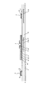
次に、上述したように第1の基板2上に形成されている多層膜の形成方法について図5−図15に基づいて説明する。なお、図5−図15は、図3に示したA−A’線に沿った領域に対応する断面図である。まず、ガラス等の透明な部材からなる第1の基板2を準備し、図5に示すように、第1の基板2の一面に、例えば、クロム、アルミニウム、モリブデン、チタン等の遮光性の金属をスパッタ法またはCVD(Chemical Vapor Deposition)法により第1の導電層40として成膜する。ここで、第1の導電層40は、層厚が例えば100〜500nmになるように成膜する。
Next, a method for forming the multilayer film formed on the
次に、第1の導電層40上にフォトレジストを塗布するとともに、露光及び現像によりこの塗布したフォトレジストをパターニングする。そして、パターニングされたフォトレジストをマスクとしてこのフォトレジストから露出された部分の第1の導電層40をエッチングし、その後、フォトレジストを剥離することにより、図6に示すように、パターニングされた第1の導電層40として、ゲート電極Gと走査線9とが形成される。
Next, a photoresist is applied onto the first
次に、パターニングされた第1の導電層40を覆うようにして、第1の基板2上に、窒化シリコン(SiNまたはSi3N4)または酸化シリコン(SiO2)等の無機絶縁材料をプラズマCVD法等により第1の絶縁層20として成膜する。ここで、例えば、第1の絶縁層20を窒化シリコンにより形成する場合、プロセスガスは、主原料ガスとしてシラン(SiH4)、副原料ガスとしてアンモニア(NH3)、希釈ガスとして窒素(N2)が用いられる。また、第1の絶縁層20は、層厚が例えば200〜800nmになるように成膜する。ここで、第1の絶縁層20は、第1の導電層40よりも層厚が厚くなるように成膜することが好ましい。
Next, an inorganic insulating material such as silicon nitride (SiN or Si 3 N 4 ) or silicon oxide (SiO 2 ) is plasma-treated on the
次に、図7に示すように、第1の絶縁層20上にプラズマCVD法等によりアモルファスシリコンまたはポリシリコンからなる半導体層21を成膜し、その後、半導体層21上に窒化シリコン(SiNまたはSi3N4)等の無機絶縁材料をプラズマCVD法等によりエッチング防止層24として成膜する。なお、第1の絶縁層20、半導体層21及びエッチング防止層24は、連続的に成膜されることが好ましい。ここで、半導体層21は、層厚が例えば20〜60nmになるように成膜する。また、エッチング防止層24は、層厚が例えば100〜200nmになるように成膜する。
Next, as shown in FIG. 7, a
次に、エッチング防止層24上にフォトレジストを塗布するとともに、露光及び現像によりこの塗布したフォトレジストをパターニングする。そして、パターニングされたフォトレジストをマスクとしてこのフォトレジストから露出された部分のエッチング防止層24をエッチングし、その後、フォトレジストを剥離することにより、薄膜トランジスタ8におけるチャネルに対応する領域に残存するようにパターニングされたエッチング防止層24が形成される(図8)。
Next, a photoresist is applied on the
次に、パターニングされたエッチング防止層24を覆うようにして、第1の基板2上にアモルファスシリコンまたはポリシリコンに不純物がドープされた比較的低抵抗な半導体をオーミックコンタクト層22として成膜し、その後、オーミックコンタクト層22上に、例えば、クロム、アルミニウム、モリブデン、チタン等の遮光性の金属からなる金属層23をスパッタ法またはCVD法により成膜する(図9)。なお、金属層23は、必ずしも、遮光性の金属に限定するものではなく、例えばITO等の透明性の導電材料であってもよい。ここで、オーミックコンタクト層22は、層厚が例えば10〜40nmになるように成膜する。また、金属層23は、層厚が例えば100〜500nmになるように成膜する。
Next, a relatively low-resistance semiconductor doped with impurities in amorphous silicon or polysilicon is formed on the
そして、上述のように、半導体層21、オーミックコンタクト層22及び金属層23が順次成膜されることによって、半導体層21、オーミックコンタクト層22及び金属層23の積層膜としての第2の導電層41が形成される。
Then, as described above, the
次に、金属層23上にフォトレジストを塗布するとともに、露光及び現像によりこの塗布したフォトレジストをパターニングする。そして、パターニングされたフォトレジストをマスクとしてこのフォトレジストから露出された部分の半導体層21、オーミックコンタクト層22及び金属層23を一括的にまたは連続的にエッチングし、その後、フォトレジストを剥離することにより、パターニングされた第2の導電層41として、ソース電極S、接続パッド部Sa、ドレイン電極D及び信号線10が形成される(図10)。なお、エッチング防止層24により覆われている領域における半導体層21は、エッチング防止層24により保護されることによってエッチングされずに残存する。そして、半導体層21、ゲート電極G、ソース電極S及びドレイン電極Dを有した薄膜トランジスタ8が形成される。
Next, a photoresist is applied on the
次に、パターニングされた第2の導電層41を覆うようにして、第1の基板2上に、窒化シリコン(SiNまたはSi3N4)または酸化シリコン(SiO2)等の無機絶縁材料をプラズマCVD法等により第2の絶縁層25として成膜する。ここで、第2の絶縁層25を窒化シリコンにより形成する場合、プロセスガスは、主原料ガスとしてシラン(SiH4)、副原料ガスとしてアンモニア(NH3)、希釈ガスとして窒素(N2)を用いることができる。ここで、第2の絶縁層25は、層厚が例えば200〜800nmになるように成膜する。
Next, an inorganic insulating material such as silicon nitride (SiN or Si 3 N 4 ) or silicon oxide (SiO 2 ) is plasma-treated on the
次に、第2の絶縁層25上に、例えば、クロム、アルミニウム、モリブデン、チタン等の遮光性の金属をスパッタ法またはCVD法により第3の導電層42として成膜する(図11)。ここで、第3の導電層42は、層厚が例えば100〜500nmになるように成膜する。
Next, a light-shielding metal such as chromium, aluminum, molybdenum, titanium, or the like is formed as the third
次に、第3の導電層42上にフォトレジストを塗布するとともに、露光及び現像によりこの塗布したフォトレジストをパターニングする。そして、パターニングされたフォトレジストをマスクとしてこのフォトレジストから露出された部分の第3の導電層42をエッチングし、その後、フォトレジストを剥離することにより、パターニングされた第3の導電層42として、補助容量電極11が形成される(図12)。
Next, a photoresist is applied on the third
次に、補助容量電極11を覆うようにして、第1の基板2上に、窒化シリコン(SiNまたはSi3N4)または酸化シリコン(SiO2)等の無機絶縁材料をプラズマCVD法等により第3の絶縁層28として成膜する。ここで、第3の絶縁層28を窒化シリコンにより形成する場合、プロセスガスは、主原料ガスとしてシラン(SiH4)、副原料ガスとしてアンモニア(NH3)、希釈ガスとして窒素(N2)を用いることができる。ここで、第3の絶縁層28は、層厚が例えば100〜600nmになるように成膜する。
Next, an inorganic insulating material such as silicon nitride (SiN or Si 3 N 4 ) or silicon oxide (SiO 2 ) is formed on the
次に、第3の絶縁層28上にフォトレジストを塗布するとともに、露光及び現像によりこの塗布したフォトレジストをパターニングする。このとき、図13に示すように、パターニングされたフォトレジスト50は、接続パッド部Saの一部が該フォトレジスト50から露出するように形成される。
Next, a photoresist is applied onto the third insulating
次に、フォトレジスト50をマスクにしてフォトレジスト50から露出された部分の第2の絶縁層25及び第3の絶縁層28を例えばドライエッチングにより一括的にエッチングすることで、図14に示すように、第2の絶縁層25にコンタクトホール25aが形成されるとともに第3の絶縁層28にコンタクトホール28aが形成される。なお、エッチングガスには、例えば、CF4、SF6、O2、He等の混合ガスを用いることができる。
Next, the portions of the second insulating
次に、フォトレジスト50を剥離し、コンタクトホールが形成された第3の絶縁層27を覆うようにして、第1の基板2上に、ITO等の透明性の導電材料をスパッタ法等により第4の導電層43として成膜する(図15)。ここで、第4の導電層43は、層厚が例えば30〜300nmになるように成膜する。
Next, the
次に、第4の導電層43上にフォトレジストを塗布するとともに、露光及び現像によりこの塗布したフォトレジストをパターニングする。そして、パターニングされたフォトレジストをマスクとしてこのフォトレジストから露出された部分の第4の導電層43をエッチングし、その後、フォトレジストを剥離することにより、パターニングされた第4の導電層43として画素電極7が形成され、図4に示したような多層膜が得られる。
Next, a photoresist is applied on the fourth
なお、上述の実施の形態では、第1の絶縁層20、第2の絶縁層25及び第3の絶縁層28を無機絶縁材料により形成する場合について説明したが、第1の絶縁層20、第2の絶縁層25及び第3の絶縁層28はポリイミド系やアクリル系の有機材料で形成してもよい。
In the above-described embodiment, the case where the first insulating
1…液晶表示素子、2,3…基板、5…液晶層、7…画素電極、8…薄膜トランジスタ、9…走査線、10…信号線、11…補助容量電極、20,25,28…絶縁層、21…半導体層、22…オーミックコンタクト層、23…金属層、24…エッチング防止層、G…ゲート電極、D…ドレイン電極、S…ソース電極
DESCRIPTION OF
Claims (20)
前記画素電極との間で補助容量を形成するとともに、少なくとも一部が前記薄膜トランジスタに重なるように配置された補助容量電極と、
を備え、
前記薄膜トランジスタは、半導体層と、該半導体層に接するように配置された絶縁性材料からなるエッチング防止層と、前記エッチング防止層との間に前記半導体層が介在するように配置されたゲート電極と、
を有し、
前記補助容量電極のうちの前記薄膜トランジスタの前記ゲート電極と重なる領域は、前記薄膜トランジスタにおけるチャネル長方向に沿う第1の方向の長さが、前記ゲート電極の前記第1の方向の長さよりも短く、且つ、前記エッチング防止層の前記第1の方向の長さよりも長いことを特徴とする液晶表示素子。 A thin film transistor in which either one of the source electrode and the drain electrode is connected to the pixel electrode;
An auxiliary capacitance formed between the pixel electrode and at least a portion of the auxiliary capacitance electrode that overlaps the thin film transistor;
With
The thin film transistor includes a semiconductor layer, an etching prevention layer made of an insulating material arranged in contact with the semiconductor layer, and a gate electrode arranged such that the semiconductor layer is interposed between the etching prevention layer ,
Have
A region of the auxiliary capacitance electrode that overlaps the gate electrode of the thin film transistor has a length in a first direction along a channel length direction of the thin film transistor that is shorter than a length of the gate electrode in the first direction. The liquid crystal display element is longer than the length of the etching prevention layer in the first direction.
前記エッチング防止層は、透光性の材料からなることを特徴とする請求項1乃至5の何れか1項に記載の液晶表示素子。 The gate electrode and the auxiliary capacitance electrode are made of a light-shielding metal,
The liquid crystal display element according to claim 1, wherein the etching prevention layer is made of a translucent material.
ソース電極及びドレイン電極の何れか一方が前記画素電極に接続された薄膜トランジスタと、
前記共通電極と等しい電位に設定されるとともに、少なくとも一部が前記薄膜トランジスタに重なるように配置された補助容量電極と、
を備え、
前記薄膜トランジスタは、半導体層と、前記半導体層に接するように配置された絶縁性材料からなるエッチング防止層と、前記エッチング防止層との間に前記半導体層が介在するように配置されたゲート電極と、を有し、
前記補助容量電極のうちの前記ゲート電極と重なる領域は、前記薄膜トランジスタにおけるチャネル長方向に沿う第1の方向の長さが、前記ゲート電極の前記第1の方向の長さよりも短く且つ前記エッチング防止層の前記第1の方向の長さよりも長いことを特徴とする液晶表示素子。 A liquid crystal layer disposed between the common electrode and the pixel electrode;
A thin film transistor in which one of a source electrode and a drain electrode is connected to the pixel electrode;
An auxiliary capacitance electrode that is set to the same potential as the common electrode and is disposed so that at least a part thereof overlaps the thin film transistor;
With
The thin film transistor includes a semiconductor layer, an etching prevention layer made of an insulating material arranged in contact with the semiconductor layer, and a gate electrode arranged so that the semiconductor layer is interposed between the etching prevention layer Have
The region of the auxiliary capacitance electrode that overlaps the gate electrode has a length in the first direction along the channel length direction of the thin film transistor that is shorter than the length of the gate electrode in the first direction, and prevents etching. A liquid crystal display element, wherein the layer is longer than the length in the first direction.
前記エッチング防止層は、透光性の材料からなることを特徴とする請求項7乃至11の何れか1項に記載の液晶表示素子。 The gate electrode and the auxiliary capacitance electrode are made of a light-shielding metal,
The liquid crystal display element according to claim 7, wherein the etching prevention layer is made of a translucent material.
ソース電極及びドレイン電極の何れか一方が画素電極に接続された薄膜トランジスタと、
前記画素電極との間で補助容量を形成するとともに、少なくとも一部が前記薄膜トランジスタに重なるように配置された補助容量電極と、
を備え、
前記薄膜トランジスタは、半導体層と、前記半導体層に接するように配置された絶縁性材料からなるエッチング防止層と、前記エッチング防止層との間に前記半導体層が介在するように配置されるとともに前記走査線に接続されたゲート電極と、を有し、
前記補助容量電極のうちの前記ゲート電極と重なる領域は、前記第1の方向に直交する第2の方向の長さが、前記ゲート電極の前記第2の方向の長さよりも短く且つ前記エッチング防止層の前記第2の方向の長さよりも長いことを特徴とする液晶表示素子。 A scan line arranged to extend in a first direction;
A thin film transistor in which either one of the source electrode and the drain electrode is connected to the pixel electrode;
An auxiliary capacitance formed between the pixel electrode and at least a portion of the auxiliary capacitance electrode that overlaps the thin film transistor;
With
The thin film transistor is disposed such that the semiconductor layer is interposed between a semiconductor layer, an etching prevention layer made of an insulating material disposed so as to be in contact with the semiconductor layer, and the etching prevention layer, and the scanning is performed. A gate electrode connected to the line,
The region of the auxiliary capacitance electrode that overlaps the gate electrode has a length in a second direction orthogonal to the first direction that is shorter than a length of the gate electrode in the second direction, and prevents etching. A liquid crystal display element, wherein the length of the layer is longer than the length in the second direction.
前記エッチング防止層は、透光性の材料からなることを特徴とする請求項13乃至17の何れか1項に記載の液晶表示素子。 The gate electrode and the auxiliary capacitance electrode are made of a light-shielding metal,
The liquid crystal display element according to claim 13, wherein the etching prevention layer is made of a translucent material.
Priority Applications (3)
| Application Number | Priority Date | Filing Date | Title |
|---|---|---|---|
| JP2010140079A JP5418421B2 (en) | 2010-06-21 | 2010-06-21 | Liquid crystal display element |
| US13/159,669 US8395717B2 (en) | 2010-06-21 | 2011-06-14 | Liquid crystal display apparatus |
| CN201110167250.0A CN102289118B (en) | 2010-06-21 | 2011-06-21 | Liquid crystal display element |
Applications Claiming Priority (1)
| Application Number | Priority Date | Filing Date | Title |
|---|---|---|---|
| JP2010140079A JP5418421B2 (en) | 2010-06-21 | 2010-06-21 | Liquid crystal display element |
Publications (3)
| Publication Number | Publication Date |
|---|---|
| JP2012003165A JP2012003165A (en) | 2012-01-05 |
| JP2012003165A5 JP2012003165A5 (en) | 2012-11-15 |
| JP5418421B2 true JP5418421B2 (en) | 2014-02-19 |
Family
ID=45328354
Family Applications (1)
| Application Number | Title | Priority Date | Filing Date |
|---|---|---|---|
| JP2010140079A Expired - Fee Related JP5418421B2 (en) | 2010-06-21 | 2010-06-21 | Liquid crystal display element |
Country Status (3)
| Country | Link |
|---|---|
| US (1) | US8395717B2 (en) |
| JP (1) | JP5418421B2 (en) |
| CN (1) | CN102289118B (en) |
Families Citing this family (12)
| Publication number | Priority date | Publication date | Assignee | Title |
|---|---|---|---|---|
| TWI518915B (en) | 2012-03-30 | 2016-01-21 | 群康科技(深圳)有限公司 | Array substrate structure and display panel and manufacturing method thereof |
| CN103365005A (en) * | 2012-03-30 | 2013-10-23 | 群康科技(深圳)有限公司 | Array substrate structure, array substrate structure manufacturing method and display panel |
| CN102751300B (en) * | 2012-06-18 | 2014-10-15 | 北京京东方光电科技有限公司 | Manufacture method of amorphous silicon flat plate X-ray senor |
| CN103199060B (en) * | 2013-02-17 | 2015-06-10 | 京东方科技集团股份有限公司 | Thin film transistor array substrate and thin film transistor array substrate manufacturing method and display device |
| JP6124668B2 (en) * | 2013-04-26 | 2017-05-10 | 三菱電機株式会社 | Thin film transistor substrate and manufacturing method thereof |
| KR102081827B1 (en) * | 2013-07-02 | 2020-04-16 | 삼성디스플레이 주식회사 | Liquid crystal display |
| JP2015072339A (en) * | 2013-10-02 | 2015-04-16 | 株式会社ジャパンディスプレイ | Liquid crystal display |
| CN108663862B (en) * | 2014-02-25 | 2020-02-07 | 群创光电股份有限公司 | Display panel |
| CN104062788A (en) * | 2014-07-10 | 2014-09-24 | 信利半导体有限公司 | Pixel structure, array substrate and liquid crystal display panel |
| JP2021128271A (en) * | 2020-02-14 | 2021-09-02 | 株式会社ジャパンディスプレイ | Display device and array substrate for display device |
| CN112599032A (en) * | 2020-12-29 | 2021-04-02 | Oppo广东移动通信有限公司 | Display screen, display screen assembly and electronic device |
| CN114879394B (en) * | 2022-04-29 | 2024-04-09 | 深圳市华星光电半导体显示技术有限公司 | Manufacturing method of display panel and display panel |
Family Cites Families (16)
| Publication number | Priority date | Publication date | Assignee | Title |
|---|---|---|---|---|
| JP3145931B2 (en) | 1996-08-26 | 2001-03-12 | 日本電気株式会社 | Thin film transistor |
| JP3716651B2 (en) | 1998-10-20 | 2005-11-16 | カシオ計算機株式会社 | Display device |
| JP3107075B2 (en) * | 1998-12-14 | 2000-11-06 | 日本電気株式会社 | Liquid crystal display |
| JP4395612B2 (en) | 2001-09-26 | 2010-01-13 | カシオ計算機株式会社 | Liquid crystal display element |
| JP4102925B2 (en) | 2003-05-15 | 2008-06-18 | カシオ計算機株式会社 | Active matrix type liquid crystal display device |
| JP2005045017A (en) * | 2003-07-22 | 2005-02-17 | Sharp Corp | Active matrix substrate and indicating device equipped with it |
| KR101001986B1 (en) * | 2003-10-30 | 2010-12-16 | 엘지디스플레이 주식회사 | Liquid crystal display device and manufacturing method thereof |
| JP4571845B2 (en) * | 2004-11-08 | 2010-10-27 | シャープ株式会社 | Substrate for liquid crystal display device, liquid crystal display device including the same, and driving method thereof |
| JP4687259B2 (en) * | 2005-06-10 | 2011-05-25 | カシオ計算機株式会社 | Liquid crystal display |
| JP2007294709A (en) * | 2006-04-26 | 2007-11-08 | Epson Imaging Devices Corp | Electro-optical device, electronic apparatus, and method of manufacturing electro-optical device |
| CN100495177C (en) * | 2006-04-30 | 2009-06-03 | 北京京东方光电科技有限公司 | TFTLCD array substrates device structure and manufacturing method therefor |
| JP4349406B2 (en) * | 2006-08-24 | 2009-10-21 | セイコーエプソン株式会社 | Electro-optical device substrate, electro-optical device, and electronic apparatus |
| JP4577318B2 (en) * | 2007-03-02 | 2010-11-10 | セイコーエプソン株式会社 | Manufacturing method of liquid crystal device |
| JP5245448B2 (en) | 2008-02-22 | 2013-07-24 | カシオ計算機株式会社 | Organic electroluminescent display device and manufacturing method thereof |
| JP4661913B2 (en) * | 2008-07-19 | 2011-03-30 | カシオ計算機株式会社 | Liquid crystal display device |
| JP4367566B2 (en) * | 2008-09-08 | 2009-11-18 | カシオ計算機株式会社 | Active matrix panel |
-
2010
- 2010-06-21 JP JP2010140079A patent/JP5418421B2/en not_active Expired - Fee Related
-
2011
- 2011-06-14 US US13/159,669 patent/US8395717B2/en not_active Expired - Fee Related
- 2011-06-21 CN CN201110167250.0A patent/CN102289118B/en not_active Expired - Fee Related
Also Published As
| Publication number | Publication date |
|---|---|
| CN102289118A (en) | 2011-12-21 |
| JP2012003165A (en) | 2012-01-05 |
| CN102289118B (en) | 2014-08-06 |
| US20110310340A1 (en) | 2011-12-22 |
| US8395717B2 (en) | 2013-03-12 |
Similar Documents
| Publication | Publication Date | Title |
|---|---|---|
| JP5418421B2 (en) | Liquid crystal display element | |
| US10707429B2 (en) | Flexible display panel and flexible display apparatus | |
| KR101055011B1 (en) | Active matrix substrate and liquid crystal display device having the same | |
| US7623194B2 (en) | Pixel structure and liquid crystal display and method for manufacturing the same | |
| US9449998B2 (en) | Manufacturing method of pixel structure with data line, scan line and gate electrode formed on the same layer | |
| US20130314636A1 (en) | Tft array substrate and forming method thereof, and display panel | |
| US8610871B2 (en) | Method for forming multilayer structure, method for manufacturing display panel, and display panel | |
| KR101555113B1 (en) | Semiconductor device and process of producing same, and display device | |
| JP5120828B2 (en) | Thin film transistor substrate and manufacturing method thereof, and liquid crystal display panel having the same and manufacturing method | |
| JP5384088B2 (en) | Display device | |
| US6921951B2 (en) | Thin film transistor and pixel structure thereof | |
| JP2007148345A (en) | Liquid crystal display device and method for manufacturing same | |
| US20100245735A1 (en) | Array substrate and manufacturing method thereof | |
| JP2010256517A (en) | Active matrix display device | |
| US7435629B2 (en) | Thin film transistor array panel and a manufacturing method thereof | |
| JP4481942B2 (en) | Thin film transistor for display device, substrate using the transistor, display device, and manufacturing method thereof | |
| JP2001217427A (en) | Thin film transistor, liquid crystal display panel and method of manufacturing thin film transistor | |
| US20150372025A1 (en) | Semiconductor device | |
| US20090224247A1 (en) | Liquid crystal display device | |
| JP4114409B2 (en) | Display device | |
| JP4367566B2 (en) | Active matrix panel | |
| WO2012176702A1 (en) | Tft substrate, method for producing same, and display device | |
| JP5707725B2 (en) | Thin film patterning method and display panel manufacturing method | |
| US10459300B2 (en) | Array substrate and a method for fabricating the same, a liquid crystal display panel | |
| JP5720124B2 (en) | Liquid crystal display element |
Legal Events
| Date | Code | Title | Description |
|---|---|---|---|
| A521 | Request for written amendment filed |
Free format text: JAPANESE INTERMEDIATE CODE: A523 Effective date: 20120927 |
|
| A621 | Written request for application examination |
Free format text: JAPANESE INTERMEDIATE CODE: A621 Effective date: 20120927 |
|
| A977 | Report on retrieval |
Free format text: JAPANESE INTERMEDIATE CODE: A971007 Effective date: 20130417 |
|
| A131 | Notification of reasons for refusal |
Free format text: JAPANESE INTERMEDIATE CODE: A131 Effective date: 20130709 |
|
| A521 | Request for written amendment filed |
Free format text: JAPANESE INTERMEDIATE CODE: A523 Effective date: 20130906 |
|
| A01 | Written decision to grant a patent or to grant a registration (utility model) |
Free format text: JAPANESE INTERMEDIATE CODE: A01 Effective date: 20131022 |
|
| A61 | First payment of annual fees (during grant procedure) |
Free format text: JAPANESE INTERMEDIATE CODE: A61 Effective date: 20131104 |
|
| LAPS | Cancellation because of no payment of annual fees |