JP5416212B2 - Device formation by epitaxial layer growth - Google Patents
Device formation by epitaxial layer growth Download PDFInfo
- Publication number
- JP5416212B2 JP5416212B2 JP2011528001A JP2011528001A JP5416212B2 JP 5416212 B2 JP5416212 B2 JP 5416212B2 JP 2011528001 A JP2011528001 A JP 2011528001A JP 2011528001 A JP2011528001 A JP 2011528001A JP 5416212 B2 JP5416212 B2 JP 5416212B2
- Authority
- JP
- Japan
- Prior art keywords
- film layer
- semiconductor material
- opening
- layer
- forming
- Prior art date
- Legal status (The legal status is an assumption and is not a legal conclusion. Google has not performed a legal analysis and makes no representation as to the accuracy of the status listed.)
- Active
Links
Images


Classifications
-
- H10P14/20—
-
- H10P14/3414—
-
- H—ELECTRICITY
- H10—SEMICONDUCTOR DEVICES; ELECTRIC SOLID-STATE DEVICES NOT OTHERWISE PROVIDED FOR
- H10D—INORGANIC ELECTRIC SEMICONDUCTOR DEVICES
- H10D62/00—Semiconductor bodies, or regions thereof, of devices having potential barriers
- H10D62/80—Semiconductor bodies, or regions thereof, of devices having potential barriers characterised by the materials
- H10D62/82—Heterojunctions
- H10D62/824—Heterojunctions comprising only Group III-V materials heterojunctions, e.g. GaN/AlGaN heterojunctions
-
- H—ELECTRICITY
- H10—SEMICONDUCTOR DEVICES; ELECTRIC SOLID-STATE DEVICES NOT OTHERWISE PROVIDED FOR
- H10F—INORGANIC SEMICONDUCTOR DEVICES SENSITIVE TO INFRARED RADIATION, LIGHT, ELECTROMAGNETIC RADIATION OF SHORTER WAVELENGTH OR CORPUSCULAR RADIATION
- H10F10/00—Individual photovoltaic cells, e.g. solar cells
- H10F10/10—Individual photovoltaic cells, e.g. solar cells having potential barriers
- H10F10/14—Photovoltaic cells having only PN homojunction potential barriers
- H10F10/142—Photovoltaic cells having only PN homojunction potential barriers comprising multiple PN homojunctions, e.g. tandem cells
- H10F10/1425—Inverted metamorphic multi-junction [IMM] photovoltaic cells
-
- H—ELECTRICITY
- H10—SEMICONDUCTOR DEVICES; ELECTRIC SOLID-STATE DEVICES NOT OTHERWISE PROVIDED FOR
- H10F—INORGANIC SEMICONDUCTOR DEVICES SENSITIVE TO INFRARED RADIATION, LIGHT, ELECTROMAGNETIC RADIATION OF SHORTER WAVELENGTH OR CORPUSCULAR RADIATION
- H10F71/00—Manufacture or treatment of devices covered by this subclass
- H10F71/121—The active layers comprising only Group IV materials
- H10F71/1212—The active layers comprising only Group IV materials consisting of germanium
-
- H—ELECTRICITY
- H10—SEMICONDUCTOR DEVICES; ELECTRIC SOLID-STATE DEVICES NOT OTHERWISE PROVIDED FOR
- H10F—INORGANIC SEMICONDUCTOR DEVICES SENSITIVE TO INFRARED RADIATION, LIGHT, ELECTROMAGNETIC RADIATION OF SHORTER WAVELENGTH OR CORPUSCULAR RADIATION
- H10F71/00—Manufacture or treatment of devices covered by this subclass
- H10F71/127—The active layers comprising only Group III-V materials, e.g. GaAs or InP
- H10F71/1276—The active layers comprising only Group III-V materials, e.g. GaAs or InP comprising growth substrates not made of Group III-V materials
-
- H—ELECTRICITY
- H10—SEMICONDUCTOR DEVICES; ELECTRIC SOLID-STATE DEVICES NOT OTHERWISE PROVIDED FOR
- H10F—INORGANIC SEMICONDUCTOR DEVICES SENSITIVE TO INFRARED RADIATION, LIGHT, ELECTROMAGNETIC RADIATION OF SHORTER WAVELENGTH OR CORPUSCULAR RADIATION
- H10F71/00—Manufacture or treatment of devices covered by this subclass
- H10F71/139—Manufacture or treatment of devices covered by this subclass using temporary substrates
-
- H10P14/27—
-
- H10P14/271—
-
- H10P14/276—
-
- H10P14/2905—
-
- H10P14/3211—
-
- H10P14/3218—
-
- H10P14/3221—
-
- H10P14/3418—
-
- H10P14/3421—
-
- Y—GENERAL TAGGING OF NEW TECHNOLOGICAL DEVELOPMENTS; GENERAL TAGGING OF CROSS-SECTIONAL TECHNOLOGIES SPANNING OVER SEVERAL SECTIONS OF THE IPC; TECHNICAL SUBJECTS COVERED BY FORMER USPC CROSS-REFERENCE ART COLLECTIONS [XRACs] AND DIGESTS
- Y02—TECHNOLOGIES OR APPLICATIONS FOR MITIGATION OR ADAPTATION AGAINST CLIMATE CHANGE
- Y02E—REDUCTION OF GREENHOUSE GAS [GHG] EMISSIONS, RELATED TO ENERGY GENERATION, TRANSMISSION OR DISTRIBUTION
- Y02E10/00—Energy generation through renewable energy sources
- Y02E10/50—Photovoltaic [PV] energy
- Y02E10/544—Solar cells from Group III-V materials
Landscapes
- Engineering & Computer Science (AREA)
- Photovoltaic Devices (AREA)
- Recrystallisation Techniques (AREA)
- General Physics & Mathematics (AREA)
- Physics & Mathematics (AREA)
- Condensed Matter Physics & Semiconductors (AREA)
- Manufacturing & Machinery (AREA)
- Computer Hardware Design (AREA)
- Microelectronics & Electronic Packaging (AREA)
- Power Engineering (AREA)
- Chemical Vapour Deposition (AREA)
- Life Sciences & Earth Sciences (AREA)
- Sustainable Energy (AREA)
- Chemical & Material Sciences (AREA)
- Materials Engineering (AREA)
Description
(関連出願の相互参照)
本出願は、2008年9月19日に出願された米国仮出願番号第61/098,597号「エピタキシャル層の成長によるデバイス形成」、2008年9月22日に出願された米国仮出願番号第61/099,074号「アスペクト比トラッピング及びエピタキシャル横方向成長を用いた発光デバイス」、2008年10月14日に出願された米国仮出願番号第61/104,466号「アスペクト比トラッピング、エピタキシャル層成長、及びウエハボンディングを用いた複合アプリケーション」を基礎とする優先権を主張するものであり、その開示内容は参照することにより本明細書に組み入れられる。
本発明は、半導体結晶材料を含む製作および構造に関するものである。例えば、半導体結晶材料を含む平坦化された表面上に形成される、改善されたエピタキシャル成長または構造に関するものである。
(Cross-reference of related applications)
This application is filed on September 19, 2008, US Provisional Application No. 61 / 098,597 “Device Formation by Growth of Epitaxial Layer”, US Provisional Application No. 61 / No. 099,074 “Light Emitting Device Using Aspect Ratio Trapping and Epitaxial Lateral Growth”, US Provisional Application No. 61 / 104,466, filed October 14, 2008 “Aspect Ratio Trapping, Epitaxial Layer Growth, and Wafer Bonding Claims based on the "composite application used", the disclosure of which is incorporated herein by reference.
The present invention relates to fabrication and structure including semiconductor crystal material. For example, it relates to an improved epitaxial growth or structure formed on a planarized surface containing semiconductor crystalline material.
本項は背景情報を提供し、以下に記述および/または主張される開示のさまざまな局面に関連した情報を紹介する。これらの背景は、先行技術の承認ではない。 This section provides background information and introduces information related to various aspects of the disclosure described and / or claimed below. These backgrounds are not prior art approvals.
基板のパターンニングを含む技術は、貫通転位が幾何学寸法によって制約される、即ち、貫通が結晶中で終端できないという事実を利用する。より小さな成長エリアへと基板をパターニングすることによって、自由な端部を別の自由な端部に近付ければ、貫通転位密度を低減することが可能である。これまでは、基板パターニングとエピタキシャル横方向成長(epitaxial lateral over growth(ELO))技術との組み合わせが、窒化ガリウム系デバイスで欠陥密度を大きく低減するために実施され、これにより、寿命の長いレーザーダイオードの製作を導いてきた。このプロセスは、実質的に、ELO領域の欠陥を排除するものであるが、極めて欠陥性の大きいシードウィンドウが残されるので、全ての欠陥を排除するために、リソグラフィステップおよびエピタキシャル成長ステップの繰り返しが必要である。同様の手段では、ペンデオエピタキシー法が基板付近のエピタキシャル領域における実質的に全ての欠陥を排除するが、1つのリソグラフィステップおよび2つのエピタキシャル成長ステップを必要とする。さらに、これらの両技術は、窒化ガリウムの横方向の成長速度が大きくなくてはならず、全てのヘテロエピタキシャル成長のシステムにおいて実施されているわけではない。 Techniques involving substrate patterning take advantage of the fact that threading dislocations are constrained by geometric dimensions, i.e., the threading cannot be terminated in the crystal. By patterning the substrate into a smaller growth area and bringing a free end closer to another free end, the threading dislocation density can be reduced. To date, a combination of substrate patterning and epitaxial lateral over growth (ELO) technology has been implemented to greatly reduce defect density in gallium nitride-based devices, thereby providing long-lived laser diodes. Has led the production of. While this process essentially eliminates defects in the ELO region, it leaves a very defective seed window and requires repeated lithography and epitaxial growth steps to eliminate all defects. It is. In a similar manner, the pendeo epitaxy method eliminates substantially all defects in the epitaxial region near the substrate, but requires one lithography step and two epitaxial growth steps. In addition, both these techniques must have a high lateral growth rate of gallium nitride and are not implemented in all heteroepitaxial growth systems.
「エピタキシャルネッキング」と呼ばれる別の公知の技術が、Landoら「High Quality Ge on Si by Epitaxial Necking」、Applied Physics Letters、Vol. 76、No. 25、April 2000によってGeオンSiヘテロ構造の製造に関して実施された。この手法は、選択エピタキシャル成長と欠陥結晶学との組み合わせを用いることによって、プロセスの簡素化を提供し、増大した横方向成長速度に頼ることなく、欠陥をパターニングマスクの開口部の側壁に追いやる。具体的には、(111)<110>ダイヤモンド立方晶滑り系においては、不整合転位は(100)成長面で<110>方向に沿って存在し、貫通セグメントは、(111)平面で<110>方向で生じる。(111)平面での<110>方向の貫通セグメントは、下層のSi(100)基板表面に対して45°の角度をなして伝搬する。よって、パターニングマスクにおける穴のアスペクト比が1を超える場合、貫通セグメントはマスク側壁によってブロックされ、Si直上に形成された低欠陥の上面Ge「団塊」となる。しかし、エピタキシャルネッキングの重要な制限の1つは、適用される領域のサイズである。以下により詳細に説明されるように、一般には、転位を側壁で終端させるために、両寸法の横方向の寸法は比較的小さくなければならない。 Another well-known technique called “epitaxial necking” is performed on the fabrication of Ge-on-Si heterostructures by Lando et al. “High Quality Ge on Si by Epitaxial Necking”, Applied Physics Letters, Vol. 76, No. 25, April 2000 It was done. This approach provides a process simplification by using a combination of selective epitaxial growth and defect crystallography, driving defects to the sidewalls of the opening of the patterning mask without resorting to increased lateral growth rates. Specifically, in the (111) <110> diamond cubic sliding system, misfit dislocations exist along the <110> direction at the (100) growth plane, and the through segment is <110 at the (111) plane. > Occurs in the direction. The penetration segment in the <110> direction on the (111) plane propagates at an angle of 45 ° with the surface of the underlying Si (100) substrate. Therefore, when the aspect ratio of the hole in the patterning mask exceeds 1, the penetrating segment is blocked by the mask side wall, resulting in a low-defect upper surface Ge “nodule” formed immediately above Si. However, one important limitation of epitaxial necking is the size of the applied region. As will be explained in more detail below, in general, the lateral dimensions of both dimensions must be relatively small in order to terminate the dislocation at the sidewall.
よって、当分野では、様々な格子不整合材料系における転位欠陥を抑制する半導体へテロ構造を製造する多目的かつ効率的な方法への要求がある。また、当分野では、機能および性能の向上のために、集積された格子不整合材料と低レベルの貫通欠陥との組み合わせを利用する半導体デバイスへの要求もある。 Thus, there is a need in the art for a versatile and efficient method of manufacturing semiconductor heterostructures that suppress dislocation defects in various lattice mismatched material systems. There is also a need in the art for semiconductor devices that utilize a combination of integrated lattice mismatch materials and low levels of through defects to improve functionality and performance.
アスペクト比トラッピング(ART)およびエピタキシャル横方向成長(ELO)を用いて、格子不整合材料などを含む基板上に、太陽電池などのデバイスを形成する方法および構造を提供する。 Methods and structures are provided for forming devices, such as solar cells, on substrates including lattice mismatch materials and the like using aspect ratio trapping (ART) and epitaxial lateral growth (ELO).
一般的に、第1の形態において、本発明の実施の形態は、構造を形成する方法を含み得る。前記方法は、第1の半導体材料を含む基板上に配置されたマスク層の第1の開口を形成するステップを含む。第1の半導体材料と格子不整合の第2の半導体材料を含む第1の膜層は、第1の開口内に形成される。第1の膜層は、マスク層の上面上に延伸する十分な厚さを有する。第2の半導体材料を含む第2の膜層は、第1の膜層上、かつ少なくとも一部のマスク層上に形成される。第1の膜層の縦方向成長速度は、第1の膜層の横方向成長速度より大きく、第2の膜層の横方向成長速度は、第2の膜層の縦方向成長速度より大きい。 In general, in the first aspect, embodiments of the invention may include a method of forming a structure. The method includes forming a first opening in a mask layer disposed on a substrate including a first semiconductor material. A first film layer including a second semiconductor material that is lattice mismatched with the first semiconductor material is formed in the first opening. The first film layer has a sufficient thickness extending on the upper surface of the mask layer. The second film layer containing the second semiconductor material is formed on the first film layer and on at least a part of the mask layer. The vertical growth rate of the first film layer is greater than the lateral growth rate of the first film layer, and the lateral growth rate of the second film layer is greater than the vertical growth rate of the second film layer.
1つ以上の下記の特徴が含まれ得る。第2開口は、第1の膜層を形成する前にマスク層に形成され得、第1の膜層は、第2の膜層を形成する前に第2開口内に形成され得る。第2の半導体材料を含む第3の層は、第1の膜層上に形成される。第3の膜層は、第1開口と第2開口との間で接合する。 One or more of the following features may be included. The second opening can be formed in the mask layer before forming the first film layer, and the first film layer can be formed in the second opening before forming the second film layer. A third layer containing the second semiconductor material is formed on the first film layer. The third film layer is bonded between the first opening and the second opening.
第1の膜層の転位欠陥は、第1の開口内にトラップされ得る。第1の膜層の縦方向成長速度は、その形成中に第1の膜層をドーピングすることで増加され得る。第1の膜層の横方向成長速度は、その形成中に第1の膜層をドーピングすることで減少され得る。第1の膜層の横方向成長速度は、その形成中に成長パラメータを調整し、第1の膜層の上面上にファセットを作製することで減少され得る。第2の膜層の縦方向成長速度の減少は、その形成中に第2の膜層をドーピングするのを含み得る。 Dislocation defects in the first film layer can be trapped in the first opening. The longitudinal growth rate of the first film layer can be increased by doping the first film layer during its formation. The lateral growth rate of the first film layer can be reduced by doping the first film layer during its formation. The lateral growth rate of the first film layer can be reduced by adjusting the growth parameters during its formation and creating facets on the top surface of the first film layer. Decreasing the vertical growth rate of the second film layer may include doping the second film layer during its formation.
第2の膜層の縦方向成長速度の減少は、その形成中に第2の膜層をドーピングし、第2の膜層に第1のタイプのファセットを形成し、かつ第2の膜層に第2のタイプのファセットを形成するのを抑制するのを含み得る。第2の膜層の横方向成長速度の増加は、その形成中に第2の膜層をドーピングするのを含み得る。第3の膜層の接合は、その形成中に第3の膜層をドーピングすることで促進され得る。第1開口と第2開口との間の第3の膜層の接合は、その形成中に第3の膜層をドーピングすることで促進され得る。 The reduction in the vertical growth rate of the second film layer is achieved by doping the second film layer during its formation, forming a first type of facet in the second film layer, and in the second film layer. Suppressing formation of a second type of facet may be included. Increasing the lateral growth rate of the second film layer may include doping the second film layer during its formation. The bonding of the third film layer can be facilitated by doping the third film layer during its formation. The bonding of the third film layer between the first opening and the second opening can be facilitated by doping the third film layer during its formation.
第3の膜層は、第2の半導体材料を含む。第3の膜層のドーピングは、第3の膜層のファセット成長を遅らせ、かつ第3の膜層の積層欠陥の形成を減少し得る。第2の半導体材料は、ゲルマニウムを含み得る。第2の半導体材料は、p型ドーパントを含み得る。第1、第2、または第3の膜層の少なくとも1つの形成は、エピタキシャル成長を含み得る。第1の膜層の形成は、四塩化ゲルマニウムを前駆体として用いることを含み得る。前記方法は、第3の膜層を形成した後、第3の膜層の上部分を除去して欠陥を除去するステップを更に含み得る。前記方法は、上部分が除去された後、第3の膜層上に光デバイスを形成するステップを更に含み得る。第1の膜層の上部は、基板の上部に非平行のファセットを規定し得る。第3の膜層は、自己平坦化が可能である。第3の膜層は、第3の膜層を主に(100)方向で成長させることで自己平坦化され得る。
The third film layer includes a second semiconductor material. The doping of the third film layer can retard the facet growth of the third film layer and reduce the formation of stacking faults in the third film layer. The second semiconductor material can include germanium. The second semiconductor material can include a p-type dopant. Formation of at least one of the first, second, or third film layer may include epitaxial growth. Formation of the first membrane layer can include using germanium tetrachloride as a precursor. The method may further include the step of removing the defect by removing the upper portion of the third film layer after forming the third film layer. The method may further include forming an optical device on the third film layer after the top portion is removed. The top of the first membrane layer may define a non-parallel facet on the top of the substrate. The third film layer can be self-planarized. The third film layer can be self-planarized by growing the third film layer mainly in the (100) direction.
前記方法は、第3の膜層の上部に第4の膜層を形成するステップを更に含み、第4の膜層は第3の半導体材料を含み得る。第5の膜層は、第4の膜層の上部に形成され、第5の膜層は第4の半導体材料を含み得る。ハンドルウエハは、第5の膜層に接合され、基板は除去され得る。第3の半導体材料および第4の半導体材料は、それぞれIII-V族材料を含み得る。基板はシリコンを含み得る。ハンドルウエハは、金属を含み得る。第3の半導体材料のバンドギャップは、第4の半導体材料のバンドギャップより大きくてもよい。前記構造は、多接合光電池を含み得る。 The method may further include forming a fourth film layer on top of the third film layer, and the fourth film layer may include a third semiconductor material. The fifth film layer may be formed on top of the fourth film layer, and the fifth film layer may include a fourth semiconductor material. The handle wafer can be bonded to the fifth film layer and the substrate can be removed. The third semiconductor material and the fourth semiconductor material may each include a III-V material. The substrate can include silicon. The handle wafer can include a metal. The band gap of the third semiconductor material may be larger than the band gap of the fourth semiconductor material. The structure can include a multi-junction photovoltaic cell.
一般的には、他の形態において、本発明の実施の形態は、構造を形成する方法を含み得る。前記方法は、基板上に配置されたマスク層に幅w1を有する開口を形成するステップを含み、基板は、第1の半導体材料を含む。第1の半導体材料と格子不整合の第2の半導体材料を含む第1の膜層は、開口内に形成され得る。第1の膜層は、マスク層の上面上に垂直に、かつ幅w1より大きい幅w2に横方向に延伸する。第1の膜層の一部は除去され、第1の膜層の残りの部分が、開口に近接した基板の第1の領域上に厚さt1を有するようにする。第2の半導体材料を含む第2の膜層は、第1の膜層上に形成され、幅w2より大きい幅w3に横方向に延伸する。第2の膜層の一部は除去され、第2の膜層の残りの部分が、開口に近接した基板の第2の領域上に厚さt2を有するようにする。 In general, in other forms, embodiments of the invention may include a method of forming a structure. The method includes forming an opening having a width w 1 in a mask layer disposed on the substrate, the substrate including a first semiconductor material. A first film layer comprising a second semiconductor material that is lattice mismatched with the first semiconductor material may be formed in the opening. The first film layer is perpendicular to the upper surface of the mask layer, and extends in the transverse direction to a width w 1 is larger than the width w 2. Some of the first film layer is removed, the remaining portion of the first film layer, to have a thickness t 1 in the first region of the substrate adjacent to the opening. Second layer comprising a second semiconductor material is formed on the first film layer is stretched in the transverse direction to a width w 2 is greater than the width w 3. Some of the second film layer is removed, the remaining portion of the second film layer, to have a thickness t 2 in the second region of the substrate adjacent to the opening.
1つ以上の下記の特徴が含まれ得る。さまざまな実施の形態において、t1はt2と等しい。第1の膜層の一部の除去は、少なくとも1つのエッチングまたは化学機械研磨を含み得る。第1の膜層の形成および第1の膜層の一部の除去のステップは、異なる機械で実行され得る。第1の膜層の形成、および第1の膜層の一部の除去のステップは、同じ機械で実行されてもよい。第2の半導体材料の転位欠陥は、開口内にトラップされ得る。基板の表面上の第1の膜層の一部は、実質的に転位欠陥がなくてもよい。第2の半導体材料の縦方向成長速度は、第2の半導体材料の横方向成長速度より大きくてもよい。 One or more of the following features may be included. In various embodiments, t 1 is equal to t 2 . Removal of a portion of the first membrane layer can include at least one etch or chemical mechanical polishing. The steps of forming the first membrane layer and removing a portion of the first membrane layer may be performed on different machines. The steps of forming the first film layer and removing a portion of the first film layer may be performed on the same machine. Dislocation defects in the second semiconductor material can be trapped in the opening. A portion of the first film layer on the surface of the substrate may be substantially free of dislocation defects. The vertical growth rate of the second semiconductor material may be greater than the lateral growth rate of the second semiconductor material.
開口の側壁は、誘電材料を含み得る。エピタキシャル成長は、第1の膜層および第2の膜層の少なくとも1つを形成するのに用いれ得る。前記方法は、第2の膜層を形成するステップ、第2の膜層の上部を除去するステップ、および/または第2の膜層上に光デバイスを形成するステップの後、四塩化ゲルマニウムを前駆体として用いて第1の膜層を形成するステップを更に含み得る。第1の膜層の上部は、基板の上面に非平行なファセットを規定し得る。第2の膜層は、自己平坦化され得る。第2の膜層は、第2の膜層を主に(100)方向で成長させることで自己平坦化され得る。 The sidewall of the opening can include a dielectric material. Epitaxial growth can be used to form at least one of the first film layer and the second film layer. The method includes the step of forming germanium tetrachloride after the steps of forming a second film layer, removing an upper portion of the second film layer, and / or forming an optical device on the second film layer. The method may further include forming a first film layer using the body. The top of the first film layer may define a facet that is non-parallel to the top surface of the substrate. The second film layer can be self-planarized. The second film layer can be self-planarized by growing the second film layer mainly in the (100) direction.
前記方法は、第2の膜層の上部に第3の膜層を形成するステップを更に含み、第3の膜層は第3の半導体材料を含み得る。第4の半導体材料を含み得る第4の膜層は、第3の膜層の上部に形成され得る。第4の膜層は、ハンドルウエハに接合され、基板は除去され得る。第3の半導体材料および第4の半導体材料は、それぞれIII-V族材料を含み得る。基板はシリコンを含み得る。ハンドルウエハは、金属を含み得る。第3の半導体材料のバンドギャップは、第4の半導体材料のバンドギャップより大きくてもよい。前記構造は、多接合光電池を含み得る。 The method may further include forming a third film layer on top of the second film layer, and the third film layer may include a third semiconductor material. A fourth film layer that may include a fourth semiconductor material may be formed on top of the third film layer. The fourth membrane layer can be bonded to the handle wafer and the substrate can be removed. The third semiconductor material and the fourth semiconductor material may each include a III-V material. The substrate can include silicon. The handle wafer can include a metal. The band gap of the third semiconductor material may be larger than the band gap of the fourth semiconductor material. The structure can include a multi-junction photovoltaic cell.
一般的には、他の形態において、本発明の実施の形態は、膜層を形成する方法を含み得る。前記方法は、基板上に配置されたマスク層に第1開口を形成するステップを含む。立方晶半導体材料を含む第1の膜層は、第1開口に形成される。第1の膜層は、基板の上面上に垂直に延伸するのに十分な厚さを有する。立方晶半導体材料をも含む第2の膜は、第1の膜層に形成される。第1の膜層の縦方向成長速度は、第1の膜層の横方向成長速度より大きく、第2の膜層の横方向成長速度は、第2の膜層の縦方向成長速度より大きい。 In general, in other forms, embodiments of the invention can include a method of forming a membrane layer. The method includes forming a first opening in a mask layer disposed on a substrate. A first film layer containing a cubic semiconductor material is formed in the first opening. The first film layer has a thickness sufficient to extend vertically on the top surface of the substrate. The second film including the cubic semiconductor material is formed in the first film layer. The vertical growth rate of the first film layer is greater than the lateral growth rate of the first film layer, and the lateral growth rate of the second film layer is greater than the vertical growth rate of the second film layer.
前記方法の実施の形態は、第1の膜層を形成する前に、マスク層に第2開口を形成するステップを更に含み得る。第2の膜層を形成する前に、第1の膜層は、第2開口内に形成され得る。第2の膜層は、第1開口と第2開口との間に接合され得る。マスク層は、半導体誘電材料を含み得る。基板の第1開口は、(110)面を含み得、基板はシリコンを含み得る。前記方法は、前記第1開口内に第1の膜層の転位欠陥をトラップするステップを更に含み得る。第2の膜層の縦方向成長速度の増加および第2の膜層の横方向成長速度の増加は、成長条件の変更を含み得る。成長条件は、0.1気圧および750℃を含み得る。 Embodiments of the method may further include forming a second opening in the mask layer before forming the first film layer. Prior to forming the second film layer, the first film layer may be formed in the second opening. The second membrane layer can be bonded between the first opening and the second opening. The mask layer can include a semiconductor dielectric material. The first opening of the substrate can include a (110) plane and the substrate can include silicon. The method may further include trapping dislocation defects in the first film layer within the first opening. Increasing the vertical growth rate of the second film layer and increasing the lateral growth rate of the second film layer may include changing growth conditions. Growth conditions may include 0.1 atmosphere and 750 ° C.
立方晶半導体材料は、ゲルマニウム、GaAs、InP、または他のIII-V族材料を含み得る。立方晶半導体材料は、ドープされ得る。第1の膜層の欠陥は、第1開口にトラップされる。デバイスは、第2の膜層に形成され得る。デバイスは、光デバイスであり得る。第2の膜層の上部は、エッチングされ得る。第1の膜層の上部は、基板の上面に非平行なファセットを規定し得る。第2の膜層は、自己平坦化され得る。第2の膜層は、第2の膜層を主に(100)方向で成長させることで自己平坦化され得る。 The cubic semiconductor material may include germanium, GaAs, InP, or other group III-V materials. The cubic semiconductor material can be doped. Defects in the first film layer are trapped in the first opening. The device can be formed in the second membrane layer. The device can be an optical device. The top of the second membrane layer can be etched. The top of the first film layer may define a facet that is non-parallel to the top surface of the substrate. The second film layer can be self-planarized. The second film layer can be self-planarized by growing the second film layer mainly in the (100) direction.
前記方法は、第2の膜層の上部に第3の膜層を形成するステップを更に含み、第3の膜層は第3の半導体材料を含み得る。第4の半導体材料を含み得る第4の膜層は、第3の膜層の上部に形成され得る。第4の膜層は、ハンドルウエハに接合され、基板は除去され得る。第3の半導体材料および第4の半導体材料は、それぞれIII-V族材料を含み得る。基板はシリコンを含み得る。ハンドルウエハは、金属を含み得る。第3の半導体材料のバンドギャップは、第4の半導体材料のバンドギャップより大きくてもよい。前記構造は、多接合光電池を含み得る。 The method may further include forming a third film layer on top of the second film layer, and the third film layer may include a third semiconductor material. A fourth film layer that may include a fourth semiconductor material may be formed on top of the third film layer. The fourth membrane layer can be bonded to the handle wafer and the substrate can be removed. The third semiconductor material and the fourth semiconductor material may each include a III-V material. The substrate can include silicon. The handle wafer can include a metal. The band gap of the third semiconductor material may be larger than the band gap of the fourth semiconductor material. The structure can include a multi-junction photovoltaic cell.
この一般的発明概念のこれらのおよび/または他の局面および有用性は、添付の図面と併せて解釈されると、以下の実施の形態の説明から明白になり、より容易に理解される。
リフトオフ技術を含む基本的なARTプロセスは、"Multi-Junction Solar Cell"と題された2008年6月26日に出願された米国特許出願番号第12/147,027号に詳細に述べられている。ART技術を用いた太陽電池の形成は、"Lattice-mismatched semiconductor structures with reduced dislocation defect densities and related methods for device fabrication"と題された2008年7月25日に出願された米国特許出願番号第12/180,254号に述べられている。 The basic ART process, including lift-off technology, is described in detail in US patent application Ser. No. 12 / 147,027 filed Jun. 26, 2008 entitled “Multi-Junction Solar Cell”. . The formation of solar cells using ART technology is based on US patent application no. 12 / filed on July 25, 2008 entitled "Lattice-mismatched semiconductor structures with reduced dislocation defect characteristics and related methods for device fabrication". No. 180,254.
不純物を用いることによって制御されたELOを用いた本発明の実施の形態が図1に述べられている。ELOは、ファセット制御を用いて、ウエハ上に実行され得る。ファセットは、例えば、材料の不純物の程度を変更、成長温度を変更、成長圧力を変更、前駆体のガス流量を変更、および/または前駆体組成物を変更することで、制御され得る。ファセット制御は、少なくとも2つの目的のために望ましい。(i)所定の縦方向成長のためにELD横方向成長を増加する、および(ii)接合時の積層欠陥または転位を低減する。1つの実施の形態において、(110)のトレンチ内に形成されたシリコン(100)ウエハ上のゲルマニウムのファセットは、周知のファセットの挙動を用いて制御され得る。同様の技術が他の材料および方向にも応用され得る。実施の形態は、ARTとELOとの組み合わせのためのファセット制御の応用を表しているが、本技術はELOのみに用いられてもよい。 An embodiment of the present invention using ELO controlled by using impurities is described in FIG. ELO can be performed on the wafer using facet control. Facets can be controlled, for example, by changing the degree of impurity in the material, changing the growth temperature, changing the growth pressure, changing the precursor gas flow rate, and / or changing the precursor composition. Facet control is desirable for at least two purposes. (I) increase ELD lateral growth for a given vertical growth, and (ii) reduce stacking faults or dislocations during bonding. In one embodiment, germanium facets on a silicon (100) wafer formed in a (110) trench can be controlled using well-known facet behavior. Similar techniques can be applied to other materials and directions. Although the embodiment represents an application of facet control for a combination of ART and ELO, the present technology may be used only for ELO.
図2に記載するように、本発明の他の実施の形態は、膜層の除去と再成長を繰り返すELOを用いている。ELOは、不整合のエピタキシーを成長させるように用いられる。最大の横方向成長の長さは、薄膜の最大許容厚さによって制限され得る。横方向成長の長さは、薄膜を繰り返し薄化して再成長させることで増加され得る。薄化と再成長のステップは、異なる機械で実行され得るか、または同じ機械で生じ得る。この技術は、ARTまたは従来のELOとともに用いられ得る。 As shown in FIG. 2, another embodiment of the present invention uses an ELO that repeats removal and regrowth of the film layer. ELO is used to grow inconsistent epitaxy. The maximum lateral growth length can be limited by the maximum allowable thickness of the thin film. The length of lateral growth can be increased by repeatedly thinning and re-growing the thin film. The thinning and regrowth steps can be performed on different machines or can occur on the same machine. This technique can be used with ART or conventional ELO.
図3に記載するように、本発明の他の実施の形態は、立方晶半導体材料の有効なELOのための方法を提供する。GaNおよび他のIII-N族半導体は、六方晶系構造を有する。横方向成長速度と縦方向成長速度との高比率(GRhorizontal / GRvertical)に有利な条件がGeなどの立方晶半導体材料、またはGaAsまたはInPなどのIII-V族材料に見られない。この実情はELOの使用をより困難にする。可能な解決法は、縦方向成長速度および横方向成長速度を選択的に制御することである。模範的なプロセスにおいて、(110)面の基板、例えば(110)面のシリコン基板で始まり得る。絶縁体は、その上に堆積され、パターン化される。ゲルマニウムまたは立方晶III-V族材料は、例えば、縦方向成長および横方向成長を促進する成長条件のもとで成長される。次いで、パラメータが<110>方向でほぼ成長させないが、<110>に垂直な方向、例えば<111>方向で著しく成長する成長条件に切り換えられる。NoborisakaらのApplied Physics Letters 86 213102 (2005)、およびNoborisakaらのApplied Physics Letters 87 093109 (2005)の文献を参照下さい。ここでのキーポイントは(110)基板を用いていることである。これは、実際には、高GRvertical / GRhorizontal から高GRhorizontal / GRverticalに変動させ、ELDに望ましい。 As described in FIG. 3, another embodiment of the present invention provides a method for effective ELO of cubic semiconductor materials. GaN and other III-N semiconductors have a hexagonal structure. Conditions advantageous for a high ratio of the horizontal growth rate to the vertical growth rate (GR horizontal / GR vertical ) are not found in cubic semiconductor materials such as Ge, or III-V group materials such as GaAs or InP. This fact makes the use of ELO more difficult. A possible solution is to selectively control the longitudinal and lateral growth rates. In an exemplary process, one may begin with a (110) plane substrate, eg, a (110) plane silicon substrate. An insulator is deposited and patterned thereon. Germanium or cubic III-V materials are grown, for example, under growth conditions that promote longitudinal and lateral growth. The parameter is then switched to a growth condition that does not grow substantially in the <110> direction, but grows significantly in a direction perpendicular to <110>, for example the <111> direction. See Noborisaka et al., Applied Physics Letters 86 213102 (2005), and Noborisaka et al., Applied Physics Letters 87 093109 (2005). The key point here is that a (110) substrate is used. This is actually desirable for ELD by varying from high GR vertical / GR horizontal to high GR horizontal / GR vertical .
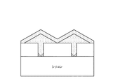
ARTおよびELOを用いることによって太陽電池の形成を含む本発明の実施の形態が図4に記載される。図4は、従来の多重接合構造のゲルマニウム基板を代替するのに用いられているGeのARTとELDとの組み合わせを表している。従来の構造において、GaAsのp/n接合およびInGaPのp/n接合は、ゲルマニウムウエハ上に成長される。InGaPのp/n接合は、高バンドギャップ(1.8eV)を有して、最も高いエネルギー光を収集し、GaAsのp/n接合は、中レベルのバンドギャップ(1.4eV)を有して、中間的なエネルギー光を収集する。従来の構造において、最も低いエネルギー光は、ゲルマニウムウエハの上部に形成されたゲルマニウムのp/n接合によって収集される。 An embodiment of the present invention involving the formation of solar cells by using ART and ELO is described in FIG. FIG. 4 shows a combination of Ge ART and ELD used to replace a conventional multi-junction structure germanium substrate. In a conventional structure, a GaAs p / n junction and an InGaP p / n junction are grown on a germanium wafer. InGaP p / n junctions have the highest bandgap (1.8 eV) and collect the highest energy light, and GaAs p / n junctions have a medium level bandgap (1.4 eV). And collect intermediate energy light. In conventional structures, the lowest energy light is collected by a germanium p / n junction formed on top of the germanium wafer.
従来の構成は、GeのARTとELOとの組み合わせがゲルマニウムウエハを代替するのに用いられた場合、うまく動作しない可能性がある。これには2つの理由がある。まず1つ目の理由は、従来の多接合構成のゲルマニウムセルは、厚過ぎる可能性がある。ゲルマニウムの熱膨張係数(CTE)は、シリコンの熱膨張係数(CTE)とかなり異なる。ゲルマニウムの成長は、通常、成長温度で応力を受けないが、冷却後、応力を受ける。ゲルマニウムが厚く成長し過ぎた場合、応力を緩和するためにゲルマニウムに亀裂を形成する可能性がある。亀裂を招く可能性のある厚さは、約5〜10ミクロンの間であり、実際の厚さは、成長温度によって決定する。従来の多接合構成に用いられるゲルマニウムセルは、少なくとも20ミクロンの厚さが望ましい。この厚さが望ましいのは、ゲルマニウムのバンドギャップは、間接であるため、ゲルマニウムがあまりよい光吸収体ではないからである。作製されたゲルマニウムセルが薄過ぎた場合、吸収されることなく、多くの光が通過する可能性があり、セルの効率を減少させる可能性がある。この厚さも電流整合により要求される。ゲルマニウムセルが薄過ぎた場合、底部セルに生成された電流は、上部セルに生成されえる電流より低い可能性があるため、一連の接続されたデバイスの電流およびその効率を減少する。 Conventional configurations may not work well when a combination of Ge ART and ELO is used to replace the germanium wafer. There are two reasons for this. The first reason is that the conventional multi-junction germanium cell may be too thick. The coefficient of thermal expansion (CTE) of germanium is quite different from that of silicon. Germanium growth is usually not stressed at the growth temperature, but is stressed after cooling. If germanium grows too thick, it may crack in germanium to relieve stress. The thickness that can lead to cracking is between about 5-10 microns, and the actual thickness is determined by the growth temperature. The germanium cell used in conventional multijunction configurations is preferably at least 20 microns thick. This thickness is desirable because germanium is not a very good light absorber because the band gap of germanium is indirect. If the fabricated germanium cell is too thin, more light can pass through without being absorbed, which can reduce the efficiency of the cell. This thickness is also required by current matching. If the germanium cell is too thin, the current generated in the bottom cell may be lower than the current that can be generated in the top cell, thus reducing the current in the series of connected devices and their efficiency.
2つ目の理由は、従来の構成がGeのARTとELOとの組み合わせとうまく動作しないのは、この構成のゲルマニウムとシリコン基板との間の高い抵抗によるものである。電流は、2つを連結する狭いトレンチを介してゲルマニウムとシリコンとの間を通過し得るだけである。トレンチを形成する酸化物は、その他のパスの電流をブロックする。この高い抵抗は、太陽電池の効率を減少する可能性がある。 The second reason is that the conventional configuration does not work well with the combination of Ge ART and ELO because of the high resistance between the germanium and silicon substrate in this configuration. The current can only pass between germanium and silicon through a narrow trench connecting the two. The oxide that forms the trench blocks the current in the other paths. This high resistance can reduce the efficiency of the solar cell.
図5aおよび図5bは、これらの問題に対処する可能な方法を述べている。反転型太陽電池は、図5aに表されているようにGeのARTとELOとの組み合わせの基板上に成長され得る。まず、高バンドギャップInGaPが成長し、次いでGaAs、次いでInGaAsが成長する。InGaAsバッファ層は、GaAsとInGaAsとの間に用いられ、InGaAsとGaAsとの間の格子定数の差を緩和する。InGaAs太陽電池は、InGaAsが直接遷移半導体であるため、一般的に2マイクロメータと、かなり薄く作製され、よって効率よく光を吸収する。セルが成長した後、ウエハは反転され、導電性のハンドルウエハに接合され得る。GeのARTとELOとの組み合わせの基板は、次いで選択エッチングによって除去され得る。選択エッチングは、除去されるシリコン基板が、除去されない化合物半導体太陽電池より遥かに厚いため、非常に正確に実行されることが望ましい。この選択エッチングは、KOHなどの非常に選択性のよいウェットエッチを用いることで達成される。これは、シリコンを速くエッチングするがゲルマニウムをゆっくりとエッチングする。薄層酸化物およびゲルマニウムのARTとELOとの組み合わせの膜層は、次いで別のステップで除去される。このステップは、これらの膜層が化合物半導体太陽電池に対して厚くないため、決して挑戦的ではない。 Figures 5a and 5b describe possible ways to address these issues. The inverted solar cell can be grown on a Ge ART and ELO combination substrate as represented in FIG. 5a. First, a high band gap InGaP is grown, then GaAs and then InGaAs. The InGaAs buffer layer is used between GaAs and InGaAs, and relaxes the difference in lattice constant between InGaAs and GaAs. InGaAs solar cells are made fairly thin, typically 2 micrometers, because InGaAs is a direct transition semiconductor, and thus absorb light efficiently. After the cell is grown, the wafer can be flipped and bonded to a conductive handle wafer. The Ge ART and ELO combination substrate can then be removed by selective etching. The selective etching is desirably performed very accurately because the silicon substrate to be removed is much thicker than the compound semiconductor solar cell that is not removed. This selective etching is achieved by using a highly selective wet etch such as KOH. This etches silicon fast but etches germanium slowly. The thin oxide and germanium ART and ELO film layers are then removed in a separate step. This step is never challenging because these film layers are not thick for compound semiconductor solar cells.
図5bは、上述の2つの問題が反転型太陽電池の方法でうまく対処されているのを示している。低エネルギー光を吸収するInGaAs太陽電池は、亀裂を生じることなく、ゲルマニウムのARTとELOとの組み合わせの基板上に成長されるほど薄い。ハンドルウエハは、太陽電池の電流の低抵抗経路を提供する。 FIG. 5b shows that the above two problems are successfully addressed by the inverted solar cell method. InGaAs solar cells that absorb low energy light are so thin that they can be grown on germanium ART and ELO substrates without cracking. The handle wafer provides a low resistance path for solar cell current.
Claims (16)
第1の半導体材料を含む基板上に配置されたマスク層に第1開口および第2開口を形成するステップ、
前記第1開口および前記第2開口内に、前記第1の半導体材料と格子不整合の第2の半導体材料を含み、前記マスク層の上面上に延伸する厚さを有する第1の膜層を形成するステップ、
前記第1の膜層上、かつ前記マスク層の少なくとも一部の上に前記第2の半導体材料を含む第2の膜層を形成するステップ、
前記第2の膜層上に前記第2の半導体材料を含む第3の膜層を形成するステップ、
前記第3の膜層の上部に、第3の半導体材料を含む第4の膜層を形成するステップ、
前記第4の膜層の上部に、第4の半導体材料を含む第5の膜層を形成するステップ、
前記第5の膜層にハンドルウエハを接合するステップ、および
前記基板を除去するステップを含み、
前記第1の膜層の縦方向成長速度は、前記第1の膜層の横方向成長速度より大きく、前記第2の膜層の横方向成長速度は、前記第2の膜層の縦方向成長速度より大きく、
前記第3の膜層は、前記第1開口と前記第2開口との間に接合され、
前記第1の膜層の転位欠陥は、前記第1開口および前記第2開口内にトラップされ、前記第3の膜層の接合は、その形成中に前記第3の膜層をドーピングすることで促進される方法。 A method of forming a structure comprising:
Forming a first opening and a second opening in a mask layer disposed on a substrate comprising a first semiconductor material;
Said first opening and said second opening, wherein the first semiconductor material and the second semiconductor material lattice mismatch, the first film layer having a top surface thickness you draw on of the mask layer Forming steps,
The first film layer, and steps of forming a second film layer comprising the second semiconductor material over at least a portion of the mask layer,
Forming a third film layer containing the second semiconductor material on the second film layer;
Forming a fourth film layer containing a third semiconductor material on top of the third film layer;
Forming a fifth film layer including a fourth semiconductor material on the fourth film layer;
Bonding a handle wafer to the fifth film layer; and
Removing the substrate;
The longitudinal growth rate of the first film layer is greater than the lateral growth rate of the first film layer, and the lateral growth rate of the second film layer is the longitudinal growth rate of the second film layer. greater than the speed rather,
The third film layer is bonded between the first opening and the second opening,
Dislocation defects in the first film layer are trapped in the first opening and the second opening, and the junction of the third film layer is performed by doping the third film layer during its formation. How to be promoted .
第1の半導体材料を含む基板上に配置されたマスク層に幅w1を有する第1開口および第2開口を形成するステップ、
前記第1開口および前記第2開口内に、前記第1の半導体材料と格子不整合の第2の半導体材料を含む、前記マスク層の上面上に垂直に、かつ幅w1より大きい幅w2に横方向に延伸する第1の膜層を形成するステップ、
前記第1の膜層の一部を除去し、前記第1の膜層の残りの部分が前記第1開口および前記第2開口に近接した前記基板の第1の領域上に厚さt1を有するようにするステップ、
前記第1の膜層上に、前記第2の半導体材料を含む第2の膜層を形成し、前記第2の半導体材料は、幅w2より大きい幅w3に横方向に延伸するステップ、
前記第2の膜層の一部を除去し、前記第2の膜層の残りの部分が前記第1開口および前記第2開口に近接した前記基板の第2の領域上に厚さt2を有するようにするステップ、
前記第2の膜層上に前記第2の半導体材料を含む第3の膜層を形成するステップ、
前記第3の膜層の上部に、第3の半導体材料を含む第4の膜層を形成するステップ、
前記第4の膜層の上部に、第4の半導体材料を含む第5の膜層を形成するステップ、
前記第5の膜層にハンドルウエハを接合するステップ、および
前記基板を除去するステップを含み、
前記第3の膜層は、前記第1開口と前記第2開口との間に接合され、
前記第1の膜層の転位欠陥は、前記第1開口および前記第2開口内にトラップされ、前記第3の膜層の接合は、その形成中に前記第3の膜層をドーピングすることで促進される方法。 A method of forming a structure comprising:
Forming a first opening and a second opening having a width w 1 in a mask layer disposed on a substrate including a first semiconductor material;
A width w 2 that is perpendicular to the top surface of the mask layer and that is greater than width w 1 includes a second semiconductor material that is lattice-mismatched with the first semiconductor material in the first opening and the second opening . Forming a first film layer extending laterally in
A portion of the first film layer is removed, and the remaining portion of the first film layer has a thickness t 1 on the first region of the substrate adjacent to the first opening and the second opening. A step of having,
Wherein the first film layer, the second second film layer is formed including a semiconductor material, said second semiconductor material, the step of stretching in the transverse direction to a width w 2 is greater than the width w 3,
A portion of the second film layer is removed, and the remaining portion of the second film layer has a thickness t 2 on the first opening and the second region of the substrate proximate to the second opening. A step of having,
Forming a third film layer containing the second semiconductor material on the second film layer;
Forming a fourth film layer containing a third semiconductor material on top of the third film layer;
Forming a fifth film layer including a fourth semiconductor material on the fourth film layer;
Bonding a handle wafer to the fifth film layer; and
Removing the substrate;
The third film layer is bonded between the first opening and the second opening,
Dislocation defects in the first film layer are trapped in the first opening and the second opening, and the junction of the third film layer is performed by doping the third film layer during its formation. How to be promoted .
Applications Claiming Priority (7)
| Application Number | Priority Date | Filing Date | Title |
|---|---|---|---|
| US9859708P | 2008-09-19 | 2008-09-19 | |
| US61/098,597 | 2008-09-19 | ||
| US9907408P | 2008-09-22 | 2008-09-22 | |
| US61/099,074 | 2008-09-22 | ||
| US10446608P | 2008-10-10 | 2008-10-10 | |
| US61/104,466 | 2008-10-10 | ||
| PCT/US2009/057493 WO2010033813A2 (en) | 2008-09-19 | 2009-09-18 | Formation of devices by epitaxial layer overgrowth |
Publications (2)
| Publication Number | Publication Date |
|---|---|
| JP2012503340A JP2012503340A (en) | 2012-02-02 |
| JP5416212B2 true JP5416212B2 (en) | 2014-02-12 |
Family
ID=42040161
Family Applications (1)
| Application Number | Title | Priority Date | Filing Date |
|---|---|---|---|
| JP2011528001A Active JP5416212B2 (en) | 2008-09-19 | 2009-09-18 | Device formation by epitaxial layer growth |
Country Status (6)
| Country | Link |
|---|---|
| US (3) | US8034697B2 (en) |
| EP (2) | EP2528087B1 (en) |
| JP (1) | JP5416212B2 (en) |
| KR (1) | KR101216541B1 (en) |
| CN (1) | CN102160145B (en) |
| WO (1) | WO2010033813A2 (en) |
Families Citing this family (67)
| Publication number | Priority date | Publication date | Assignee | Title |
|---|---|---|---|---|
| US8324660B2 (en) | 2005-05-17 | 2012-12-04 | Taiwan Semiconductor Manufacturing Company, Ltd. | Lattice-mismatched semiconductor structures with reduced dislocation defect densities and related methods for device fabrication |
| US9153645B2 (en) | 2005-05-17 | 2015-10-06 | Taiwan Semiconductor Manufacturing Company, Ltd. | Lattice-mismatched semiconductor structures with reduced dislocation defect densities and related methods for device fabrication |
| US7777250B2 (en) | 2006-03-24 | 2010-08-17 | Taiwan Semiconductor Manufacturing Company, Ltd. | Lattice-mismatched semiconductor structures and related methods for device fabrication |
| WO2008030574A1 (en) | 2006-09-07 | 2008-03-13 | Amberwave Systems Corporation | Defect reduction using aspect ratio trapping |
| WO2008039534A2 (en) | 2006-09-27 | 2008-04-03 | Amberwave Systems Corporation | Quantum tunneling devices and circuits with lattice- mismatched semiconductor structures |
| US8502263B2 (en) | 2006-10-19 | 2013-08-06 | Taiwan Semiconductor Manufacturing Company, Ltd. | Light-emitter-based devices with lattice-mismatched semiconductor structures |
| US9508890B2 (en) | 2007-04-09 | 2016-11-29 | Taiwan Semiconductor Manufacturing Company, Ltd. | Photovoltaics on silicon |
| US7825328B2 (en) | 2007-04-09 | 2010-11-02 | Taiwan Semiconductor Manufacturing Company, Ltd. | Nitride-based multi-junction solar cell modules and methods for making the same |
| US8304805B2 (en) | 2009-01-09 | 2012-11-06 | Taiwan Semiconductor Manufacturing Company, Ltd. | Semiconductor diodes fabricated by aspect ratio trapping with coalesced films |
| US8237151B2 (en) | 2009-01-09 | 2012-08-07 | Taiwan Semiconductor Manufacturing Company, Ltd. | Diode-based devices and methods for making the same |
| US8329541B2 (en) | 2007-06-15 | 2012-12-11 | Taiwan Semiconductor Manufacturing Company, Ltd. | InP-based transistor fabrication |
| DE112008002387B4 (en) | 2007-09-07 | 2022-04-07 | Taiwan Semiconductor Manufacturing Co., Ltd. | Structure of a multijunction solar cell, method of forming a photonic device, photovoltaic multijunction cell and photovoltaic multijunction cell device, |
| US8183667B2 (en) | 2008-06-03 | 2012-05-22 | Taiwan Semiconductor Manufacturing Co., Ltd. | Epitaxial growth of crystalline material |
| US8274097B2 (en) | 2008-07-01 | 2012-09-25 | Taiwan Semiconductor Manufacturing Company, Ltd. | Reduction of edge effects from aspect ratio trapping |
| US8981427B2 (en) | 2008-07-15 | 2015-03-17 | Taiwan Semiconductor Manufacturing Company, Ltd. | Polishing of small composite semiconductor materials |
| JP5416212B2 (en) * | 2008-09-19 | 2014-02-12 | 台湾積體電路製造股▲ふん▼有限公司 | Device formation by epitaxial layer growth |
| US20100072515A1 (en) | 2008-09-19 | 2010-03-25 | Amberwave Systems Corporation | Fabrication and structures of crystalline material |
| US8253211B2 (en) | 2008-09-24 | 2012-08-28 | Taiwan Semiconductor Manufacturing Company, Ltd. | Semiconductor sensor structures with reduced dislocation defect densities |
| EP2415083B1 (en) | 2009-04-02 | 2017-06-21 | Taiwan Semiconductor Manufacturing Company, Ltd. | Devices formed from a non-polar plane of a crystalline material and method of making the same |
| US9484197B2 (en) | 2009-10-23 | 2016-11-01 | The Royal Institution For The Advancement Of Learning/Mcgill University | Lateral growth semiconductor method and devices |
| TWI562195B (en) | 2010-04-27 | 2016-12-11 | Pilegrowth Tech S R L | Dislocation and stress management by mask-less processes using substrate patterning and methods for device fabrication |
| KR101278117B1 (en) * | 2010-05-20 | 2013-06-24 | 아주대학교산학협력단 | Multi-Junction Solar Cells and Fabrication Method thereof |
| US8604330B1 (en) | 2010-12-06 | 2013-12-10 | 4Power, Llc | High-efficiency solar-cell arrays with integrated devices and methods for forming them |
| CN102790006B (en) * | 2011-05-17 | 2014-09-17 | 中国科学院微电子研究所 | Semiconductor structure and fabrication method thereof |
| US8383485B2 (en) | 2011-07-13 | 2013-02-26 | Taiwan Semiconductor Manufacturing Co., Ltd. | Epitaxial process for forming semiconductor devices |
| US8481341B2 (en) * | 2011-11-05 | 2013-07-09 | Tokyo Electron Limited | Epitaxial film growth in retrograde wells for semiconductor devices |
| CN102534768B (en) * | 2012-02-14 | 2015-03-11 | 中国科学院半导体研究所 | Method for preparing silicon-based gallium arsenide material |
| JP6207170B2 (en) * | 2012-02-15 | 2017-10-04 | アイメックImec | Mask structure and method for defect-free heteroepitaxial |
| US9142400B1 (en) | 2012-07-17 | 2015-09-22 | Stc.Unm | Method of making a heteroepitaxial layer on a seed area |
| US8878251B2 (en) * | 2012-10-17 | 2014-11-04 | Seoul National University R&Db Foundation | Silicon-compatible compound junctionless field effect transistor |
| KR102083495B1 (en) | 2013-01-07 | 2020-03-02 | 삼성전자 주식회사 | Complementary Metal Oxide Semiconductor device, optical apparatus comprising CMOS device and method of manufacturing the same |
| WO2014140082A1 (en) | 2013-03-13 | 2014-09-18 | Pilegrowth Tech S.R.L. | High efficiency solar cells on silicon substrates |
| US8916445B1 (en) | 2013-08-16 | 2014-12-23 | International Business Machines Corporation | Semiconductor devices and methods of manufacture |
| EP2849219A1 (en) | 2013-09-11 | 2015-03-18 | IMEC vzw | Method for manufacturing transistors and associated substrate |
| US9064699B2 (en) | 2013-09-30 | 2015-06-23 | Samsung Electronics Co., Ltd. | Methods of forming semiconductor patterns including reduced dislocation defects and devices formed using such methods |
| KR101464086B1 (en) * | 2013-10-18 | 2014-11-25 | 희성전자 주식회사 | Solar cell structure using multiple junction compound |
| WO2015100245A1 (en) | 2013-12-23 | 2015-07-02 | University Of Houston System | Flexible single-crystalline semiconductor device and fabrication methods thereof |
| US9177967B2 (en) * | 2013-12-24 | 2015-11-03 | Intel Corporation | Heterogeneous semiconductor material integration techniques |
| KR102168969B1 (en) | 2014-02-28 | 2020-10-22 | 삼성전자주식회사 | Semiconductor device and method for fabricating the same |
| US9287115B2 (en) | 2014-03-12 | 2016-03-15 | International Business Machines Corporation | Planar III-V field effect transistor (FET) on dielectric layer |
| EP3123514B1 (en) * | 2014-03-28 | 2022-12-21 | Intel Corporation | Strain compensation in transistors |
| FR3023058B1 (en) * | 2014-06-30 | 2017-09-29 | Commissariat Energie Atomique | METHOD FOR PRODUCING A MICROELECTRONIC DEVICE |
| GB201415119D0 (en) | 2014-08-27 | 2014-10-08 | Ibm | Method for fabricating a semiconductor structure |
| US9711683B2 (en) * | 2014-09-26 | 2017-07-18 | Epistar Corporation | Semiconductor device and the method of manufacturing the same |
| US9349808B2 (en) | 2014-09-29 | 2016-05-24 | International Business Machines Corporation | Double aspect ratio trapping |
| KR102284657B1 (en) * | 2015-01-05 | 2021-08-02 | 삼성전자 주식회사 | Photodiode and optical communication system including the same |
| US9564373B2 (en) | 2015-02-27 | 2017-02-07 | International Business Machines Corporation | Forming a CMOS with dual strained channels |
| US9401583B1 (en) | 2015-03-30 | 2016-07-26 | International Business Machines Corporation | Laser structure on silicon using aspect ratio trapping growth |
| US9583599B2 (en) | 2015-04-22 | 2017-02-28 | International Business Machines Corporation | Forming a fin using double trench epitaxy |
| US9633908B2 (en) | 2015-06-16 | 2017-04-25 | International Business Machines Corporation | Method for forming a semiconductor structure containing high mobility semiconductor channel materials |
| US9917414B2 (en) | 2015-07-15 | 2018-03-13 | International Business Machines Corporation | Monolithic nanophotonic device on a semiconductor substrate |
| CN106784127B (en) * | 2015-11-20 | 2019-02-01 | 北京创昱科技有限公司 | A kind of binode Thinfilm solar cell assembly and preparation method thereof |
| US9704958B1 (en) * | 2015-12-18 | 2017-07-11 | International Business Machines Corporation | III-V field effect transistor on a dielectric layer |
| KR102430501B1 (en) | 2015-12-29 | 2022-08-09 | 삼성전자주식회사 | Semiconductor single crystal sturucture, semiconductor device and method of fabricating the same |
| US9997475B2 (en) | 2016-01-13 | 2018-06-12 | International Business Machines Corporation | Monolithic integration of III-V cells for powering memory erasure devices |
| FR3047354B1 (en) | 2016-01-29 | 2018-05-18 | Commissariat A L'energie Atomique Et Aux Energies Alternatives | PHOTOVOLTAIC CELL AND METHOD OF MANUFACTURING PHOTOVOLTAIC CELL |
| US9564452B1 (en) | 2016-02-01 | 2017-02-07 | International Business Machines Corporation | Fabrication of hybrid semiconductor circuits |
| US9704757B1 (en) | 2016-02-25 | 2017-07-11 | International Business Machines Corporation | Fabrication of semiconductor structures |
| US9735010B1 (en) | 2016-05-27 | 2017-08-15 | International Business Machines Corporation | Fabrication of semiconductor fin structures |
| US10249492B2 (en) | 2016-05-27 | 2019-04-02 | International Business Machines Corporation | Fabrication of compound semiconductor structures |
| EP3506000B1 (en) * | 2017-12-29 | 2020-10-07 | IMEC vzw | Iii-v semiconductor waveguide nanoridge structure |
| US10978632B2 (en) | 2019-01-18 | 2021-04-13 | Microsoft Technology Licensing, Llc | Fabrication of a device |
| US10777728B2 (en) | 2019-01-18 | 2020-09-15 | Microsoft Technology Licensing, Llc | Fabrication of a quantum device |
| US11742203B2 (en) | 2020-02-26 | 2023-08-29 | The Hong Kong University Of Science And Technology | Method for growing III-V compound semiconductor thin films on silicon-on-insulators |
| TWI864562B (en) * | 2022-01-27 | 2024-12-01 | 日商京瓷股份有限公司 | Semiconductor substrate manufacturing method, manufacturing device, and control device |
| US20240347561A1 (en) * | 2022-11-10 | 2024-10-17 | The Board Of Trustees Of The University Of Arkansas | Visible to longwave infrared photodetector on silicon |
| WO2024158874A2 (en) * | 2023-01-24 | 2024-08-02 | The Regents Of The University Of Michigan | Ferroelectric iii-nitride layer thickness scaling |
Family Cites Families (403)
| Publication number | Priority date | Publication date | Assignee | Title |
|---|---|---|---|---|
| US660928A (en) * | 1900-03-30 | 1900-10-30 | Star And Crescent Mills Company | Heddle mechanism for looms. |
| US6153010A (en) | 1997-04-11 | 2000-11-28 | Nichia Chemical Industries Ltd. | Method of growing nitride semiconductors, nitride semiconductor substrate and nitride semiconductor device |
| US4307510A (en) | 1980-03-12 | 1981-12-29 | The United States Of America As Represented By The Administrator Of The National Aeronautics & Space Administration | Computer circuit card puller |
| EP0049286B1 (en) | 1980-04-10 | 1988-03-02 | Massachusetts Institute Of Technology | Methods of producing sheets of crystalline material and devices amde therefrom |
| US4322253A (en) | 1980-04-30 | 1982-03-30 | Rca Corporation | Method of making selective crystalline silicon regions containing entrapped hydrogen by laser treatment |
| US4370510A (en) | 1980-09-26 | 1983-01-25 | California Institute Of Technology | Gallium arsenide single crystal solar cell structure and method of making |
| US4545109A (en) | 1983-01-21 | 1985-10-08 | Rca Corporation | Method of making a gallium arsenide field effect transistor |
| US4651179A (en) | 1983-01-21 | 1987-03-17 | Rca Corporation | Low resistance gallium arsenide field effect transistor |
| US5091333A (en) | 1983-09-12 | 1992-02-25 | Massachusetts Institute Of Technology | Reducing dislocations in semiconductors utilizing repeated thermal cycling during multistage epitaxial growth |
| US4860081A (en) | 1984-06-28 | 1989-08-22 | Gte Laboratories Incorporated | Semiconductor integrated circuit structure with insulative partitions |
| US4551394A (en) | 1984-11-26 | 1985-11-05 | Honeywell Inc. | Integrated three-dimensional localized epitaxial growth of Si with localized overgrowth of GaAs |
| CA1292550C (en) | 1985-09-03 | 1991-11-26 | Masayoshi Umeno | Epitaxial gallium arsenide semiconductor wafer and method of producing the same |
| US4774205A (en) | 1986-06-13 | 1988-09-27 | Massachusetts Institute Of Technology | Monolithic integration of silicon and gallium arsenide devices |
| JPS6381855A (en) | 1986-09-25 | 1988-04-12 | Mitsubishi Electric Corp | Manufacturing method of heterojunction bipolar transistor |
| US5269876A (en) | 1987-01-26 | 1993-12-14 | Canon Kabushiki Kaisha | Process for producing crystal article |
| US5236546A (en) | 1987-01-26 | 1993-08-17 | Canon Kabushiki Kaisha | Process for producing crystal article |
| US5281283A (en) | 1987-03-26 | 1994-01-25 | Canon Kabushiki Kaisha | Group III-V compound crystal article using selective epitaxial growth |
| US5166767A (en) | 1987-04-14 | 1992-11-24 | National Semiconductor Corporation | Sidewall contact bipolar transistor with controlled lateral spread of selectively grown epitaxial layer |
| US4876210A (en) | 1987-04-30 | 1989-10-24 | The University Of Delaware | Solution growth of lattice mismatched and solubility mismatched heterostructures |
| US4826784A (en) | 1987-11-13 | 1989-05-02 | Kopin Corporation | Selective OMCVD growth of compound semiconductor materials on silicon substrates |
| US5079616A (en) | 1988-02-11 | 1992-01-07 | Gte Laboratories Incorporated | Semiconductor structure |
| US5272105A (en) | 1988-02-11 | 1993-12-21 | Gte Laboratories Incorporated | Method of manufacturing an heteroepitaxial semiconductor structure |
| GB2215514A (en) | 1988-03-04 | 1989-09-20 | Plessey Co Plc | Terminating dislocations in semiconductor epitaxial layers |
| US5032893A (en) | 1988-04-01 | 1991-07-16 | Cornell Research Foundation, Inc. | Method for reducing or eliminating interface defects in mismatched semiconductor eiplayers |
| US5156995A (en) | 1988-04-01 | 1992-10-20 | Cornell Research Foundation, Inc. | Method for reducing or eliminating interface defects in mismatched semiconductor epilayers |
| US5238869A (en) | 1988-07-25 | 1993-08-24 | Texas Instruments Incorporated | Method of forming an epitaxial layer on a heterointerface |
| EP0352472A3 (en) | 1988-07-25 | 1991-02-06 | Texas Instruments Incorporated | Heteroepitaxy of lattice-mismatched semiconductor materials |
| JPH0262090A (en) | 1988-08-29 | 1990-03-01 | Matsushita Electric Ind Co Ltd | Method for manufacturing optical semiconductor devices |
| US5061644A (en) | 1988-12-22 | 1991-10-29 | Honeywell Inc. | Method for fabricating self-aligned semiconductor devices |
| EP0380815B1 (en) | 1989-01-31 | 1994-05-25 | Agfa-Gevaert N.V. | Integration of GaAs on Si substrate |
| US5034337A (en) | 1989-02-10 | 1991-07-23 | Texas Instruments Incorporated | Method of making an integrated circuit that combines multi-epitaxial power transistors with logic/analog devices |
| US4948456A (en) | 1989-06-09 | 1990-08-14 | Delco Electronics Corporation | Confined lateral selective epitaxial growth |
| US5098850A (en) | 1989-06-16 | 1992-03-24 | Canon Kabushiki Kaisha | Process for producing substrate for selective crystal growth, selective crystal growth process and process for producing solar battery by use of them |
| US5256594A (en) | 1989-06-16 | 1993-10-26 | Intel Corporation | Masking technique for depositing gallium arsenide on silicon |
| US5093699A (en) | 1990-03-12 | 1992-03-03 | Texas A & M University System | Gate adjusted resonant tunnel diode device and method of manufacture |
| US5164359A (en) | 1990-04-20 | 1992-11-17 | Eaton Corporation | Monolithic integrated circuit having compound semiconductor layer epitaxially grown on ceramic substrate |
| US5158907A (en) * | 1990-08-02 | 1992-10-27 | At&T Bell Laboratories | Method for making semiconductor devices with low dislocation defects |
| US5105247A (en) | 1990-08-03 | 1992-04-14 | Cavanaugh Marion E | Quantum field effect device with source extension region formed under a gate and between the source and drain regions |
| JP3202223B2 (en) | 1990-11-27 | 2001-08-27 | 日本電気株式会社 | Method for manufacturing transistor |
| US5403751A (en) | 1990-11-29 | 1995-04-04 | Canon Kabushiki Kaisha | Process for producing a thin silicon solar cell |
| US5223043A (en) | 1991-02-11 | 1993-06-29 | The United States Of America As Represented By The United States Department Of Energy | Current-matched high-efficiency, multijunction monolithic solar cells |
| US5091767A (en) | 1991-03-18 | 1992-02-25 | At&T Bell Laboratories | Article comprising a lattice-mismatched semiconductor heterostructure |
| JPH04299569A (en) | 1991-03-27 | 1992-10-22 | Nec Corp | Manufacture of sois and transistor and its manufacture |
| US5269852A (en) | 1991-05-27 | 1993-12-14 | Canon Kabushiki Kaisha | Crystalline solar cell and method for producing the same |
| JP3058954B2 (en) | 1991-09-24 | 2000-07-04 | ローム株式会社 | Method of manufacturing semiconductor device having growth layer on insulating layer |
| JP2773487B2 (en) | 1991-10-15 | 1998-07-09 | 日本電気株式会社 | Tunnel transistor |
| JPH05121317A (en) | 1991-10-24 | 1993-05-18 | Rohm Co Ltd | Method for forming soi structure |
| JP3286920B2 (en) | 1992-07-10 | 2002-05-27 | 富士通株式会社 | Method for manufacturing semiconductor device |
| DE59308841D1 (en) | 1992-12-04 | 1998-09-10 | Siemens Ag | Method for producing a laterally delimited, single-crystalline region by means of selective epitaxy and its application for producing a bipolar transistor and a MOS transistor |
| JP3319472B2 (en) | 1992-12-07 | 2002-09-03 | 富士通株式会社 | Semiconductor device and manufacturing method thereof |
| US5295150A (en) | 1992-12-11 | 1994-03-15 | Eastman Kodak Company | Distributed feedback-channeled substrate planar semiconductor laser |
| US5407491A (en) | 1993-04-08 | 1995-04-18 | University Of Houston | Tandem solar cell with improved tunnel junction |
| EP0627799B1 (en) | 1993-06-04 | 1997-10-08 | Sharp Kabushiki Kaisha | Semiconductor light-emitting device with third cladding layer |
| JP3748905B2 (en) | 1993-08-27 | 2006-02-22 | 三洋電機株式会社 | Quantum effect device |
| US5792679A (en) | 1993-08-30 | 1998-08-11 | Sharp Microelectronics Technology, Inc. | Method for forming silicon-germanium/Si/silicon dioxide heterostructure using germanium implant |
| US5461243A (en) | 1993-10-29 | 1995-10-24 | International Business Machines Corporation | Substrate for tensilely strained semiconductor |
| US5405453A (en) | 1993-11-08 | 1995-04-11 | Applied Solar Energy Corporation | High efficiency multi-junction solar cell |
| US5489539A (en) | 1994-01-10 | 1996-02-06 | Hughes Aircraft Company | Method of making quantum well structure with self-aligned gate |
| JPH07230952A (en) | 1994-02-16 | 1995-08-29 | Ricoh Co Ltd | Recrystallization method |
| JPH0851109A (en) | 1994-04-11 | 1996-02-20 | Texas Instr Inc <Ti> | Method for growing epitaxial silicon in windows of an oxide patterned wafer |
| US6011271A (en) | 1994-04-28 | 2000-01-04 | Fujitsu Limited | Semiconductor device and method of fabricating the same |
| US5710436A (en) | 1994-09-27 | 1998-01-20 | Kabushiki Kaisha Toshiba | Quantum effect device |
| US5825240A (en) | 1994-11-30 | 1998-10-20 | Massachusetts Institute Of Technology | Resonant-tunneling transmission line technology |
| JP3835225B2 (en) | 1995-02-23 | 2006-10-18 | 日亜化学工業株式会社 | Nitride semiconductor light emitting device |
| US5528209A (en) | 1995-04-27 | 1996-06-18 | Hughes Aircraft Company | Monolithic microwave integrated circuit and method |
| JPH08306700A (en) | 1995-04-27 | 1996-11-22 | Nec Corp | Semiconductor device and manufacturing method thereof |
| TW304310B (en) | 1995-05-31 | 1997-05-01 | Siemens Ag | |
| US5621227A (en) | 1995-07-18 | 1997-04-15 | Discovery Semiconductors, Inc. | Method and apparatus for monolithic optoelectronic integrated circuit using selective epitaxy |
| JPH11500873A (en) | 1995-12-15 | 1999-01-19 | フィリップス エレクトロニクス ネムローゼ フェンノートシャップ | Semiconductor field-effect device with SiGe layer |
| TW314621B (en) | 1995-12-20 | 1997-09-01 | Toshiba Co Ltd | |
| US5987590A (en) | 1996-04-02 | 1999-11-16 | Texas Instruments Incorporated | PC circuits, systems and methods |
| EP0807980B1 (en) | 1996-05-17 | 2006-06-21 | Canon Kabushiki Kaisha | Photovoltaic device and process for the production thereof |
| JP3719618B2 (en) | 1996-06-17 | 2005-11-24 | 松下電器産業株式会社 | Semiconductor device and manufacturing method thereof |
| US6229153B1 (en) | 1996-06-21 | 2001-05-08 | Wisconsin Alumni Research Corporation | High peak current density resonant tunneling diode |
| JP3260660B2 (en) | 1996-08-22 | 2002-02-25 | 株式会社東芝 | Semiconductor device and manufacturing method thereof |
| JP3449516B2 (en) | 1996-08-30 | 2003-09-22 | 株式会社リコー | Semiconductor multilayer mirror, semiconductor multilayer antireflection film, surface emitting semiconductor laser, and light receiving element |
| US6191432B1 (en) | 1996-09-02 | 2001-02-20 | Kabushiki Kaisha Toshiba | Semiconductor device and memory device |
| US5825049A (en) | 1996-10-09 | 1998-10-20 | Sandia Corporation | Resonant tunneling device with two-dimensional quantum well emitter and base layers |
| JPH10126010A (en) | 1996-10-23 | 1998-05-15 | Ricoh Co Ltd | Method of manufacturing semiconductor laser device |
| SG65697A1 (en) | 1996-11-15 | 1999-06-22 | Canon Kk | Process for producing semiconductor article |
| US5853497A (en) | 1996-12-12 | 1998-12-29 | Hughes Electronics Corporation | High efficiency multi-junction solar cells |
| US6348096B1 (en) | 1997-03-13 | 2002-02-19 | Nec Corporation | Method for manufacturing group III-V compound semiconductors |
| JP3853905B2 (en) | 1997-03-18 | 2006-12-06 | 株式会社東芝 | Quantum effect device and device using BL tunnel element |
| EP0874405A3 (en) | 1997-03-25 | 2004-09-15 | Mitsubishi Cable Industries, Ltd. | GaN group crystal base member having low dislocation density, use thereof and manufacturing methods thereof |
| CN1131548C (en) | 1997-04-04 | 2003-12-17 | 松下电器产业株式会社 | Ohmic electrode forming method and semiconductor device |
| JP3047852B2 (en) | 1997-04-04 | 2000-06-05 | 松下電器産業株式会社 | Semiconductor device |
| JP3184115B2 (en) | 1997-04-11 | 2001-07-09 | 松下電器産業株式会社 | Ohmic electrode formation method |
| US5998781A (en) | 1997-04-30 | 1999-12-07 | Sandia Corporation | Apparatus for millimeter-wave signal generation |
| US5903170A (en) | 1997-06-03 | 1999-05-11 | The Regents Of The University Of Michigan | Digital logic design using negative differential resistance diodes and field-effect transistors |
| US5883549A (en) | 1997-06-20 | 1999-03-16 | Hughes Electronics Corporation | Bipolar junction transistor (BJT)--resonant tunneling diode (RTD) oscillator circuit and method |
| JP3535527B2 (en) | 1997-06-24 | 2004-06-07 | マサチューセッツ インスティテュート オブ テクノロジー | Controlling threading dislocations in germanium-on-silicon using graded GeSi layer and planarization |
| US5869845A (en) | 1997-06-26 | 1999-02-09 | Texas Instruments Incorporated | Resonant tunneling memory |
| US6015979A (en) | 1997-08-29 | 2000-01-18 | Kabushiki Kaisha Toshiba | Nitride-based semiconductor element and method for manufacturing the same |
| JP3930161B2 (en) | 1997-08-29 | 2007-06-13 | 株式会社東芝 | Nitride-based semiconductor device, light-emitting device, and manufacturing method thereof |
| WO1999014804A1 (en) | 1997-09-16 | 1999-03-25 | Massachusetts Institute Of Technology | CO-PLANAR Si AND Ge COMPOSITE SUBSTRATE AND METHOD OF PRODUCING SAME |
| FR2769924B1 (en) * | 1997-10-20 | 2000-03-10 | Centre Nat Rech Scient | PROCESS FOR MAKING AN EPITAXIAL LAYER OF GALLIUM NITRIDE, EPITAXIAL LAYER OF GALLIUM NITRIDE AND OPTOELECTRONIC COMPONENT PROVIDED WITH SUCH A LAYER |
| JP5065625B2 (en) * | 1997-10-30 | 2012-11-07 | 住友電気工業株式会社 | Manufacturing method of GaN single crystal substrate |
| KR100629558B1 (en) | 1997-10-30 | 2006-09-27 | 스미토모덴키고교가부시키가이샤 | BANN single crystal substrate and its manufacturing method |
| JP3180743B2 (en) | 1997-11-17 | 2001-06-25 | 日本電気株式会社 | Nitride compound semiconductor light emitting device and method of manufacturing the same |
| JP3468082B2 (en) | 1998-02-26 | 2003-11-17 | 日亜化学工業株式会社 | Nitride semiconductor device |
| US6150242A (en) | 1998-03-25 | 2000-11-21 | Texas Instruments Incorporated | Method of growing crystalline silicon overlayers on thin amorphous silicon oxide layers and forming by method a resonant tunneling diode |
| JPH11274467A (en) | 1998-03-26 | 1999-10-08 | Murata Mfg Co Ltd | Optoelectronic integrated circuit device |
| US6500257B1 (en) | 1998-04-17 | 2002-12-31 | Agilent Technologies, Inc. | Epitaxial material grown laterally within a trench and method for producing same |
| JP3338778B2 (en) | 1998-04-24 | 2002-10-28 | 日本電気株式会社 | Nitride compound semiconductor laser device |
| US6265289B1 (en) | 1998-06-10 | 2001-07-24 | North Carolina State University | Methods of fabricating gallium nitride semiconductor layers by lateral growth from sidewalls into trenches, and gallium nitride semiconductor structures fabricated thereby |
| TW417315B (en) * | 1998-06-18 | 2001-01-01 | Sumitomo Electric Industries | GaN single crystal substrate and its manufacture method of the same |
| JP4005701B2 (en) | 1998-06-24 | 2007-11-14 | シャープ株式会社 | Method of forming nitrogen compound semiconductor film and nitrogen compound semiconductor element |
| WO2000004615A1 (en) | 1998-07-14 | 2000-01-27 | Fujitsu Limited | Semiconductor laser, semiconductor device, and method for manufacturing the same |
| CA2343105C (en) | 1998-09-10 | 2004-09-28 | Rohm Co., Ltd. | Semiconductor light-emitting device and method for manufacturing the same |
| US6252261B1 (en) | 1998-09-30 | 2001-06-26 | Nec Corporation | GaN crystal film, a group III element nitride semiconductor wafer and a manufacturing process therefor |
| US6255198B1 (en) * | 1998-11-24 | 2001-07-03 | North Carolina State University | Methods of fabricating gallium nitride microelectronic layers on silicon layers and gallium nitride microelectronic structures formed thereby |
| JP3868136B2 (en) | 1999-01-20 | 2007-01-17 | 日亜化学工業株式会社 | Gallium nitride compound semiconductor light emitting device |
| JP3372226B2 (en) | 1999-02-10 | 2003-01-27 | 日亜化学工業株式会社 | Nitride semiconductor laser device |
| US7145167B1 (en) | 2000-03-11 | 2006-12-05 | International Business Machines Corporation | High speed Ge channel heterostructures for field effect devices |
| JP3760663B2 (en) | 1999-03-31 | 2006-03-29 | 豊田合成株式会社 | Method for producing group III nitride compound semiconductor device |
| JP3702700B2 (en) | 1999-03-31 | 2005-10-05 | 豊田合成株式会社 | Group III nitride compound semiconductor device and method for manufacturing the same |
| DE10017137A1 (en) | 1999-04-14 | 2000-10-26 | Siemens Ag | Novel silicon structure, used for solar cells or LCD TFTs, comprises a crystalline textured silicon thin film over a biaxially textured lattice-matched diffusion barrier buffer layer on a thermal expansion-matched inert substrate |
| US6803598B1 (en) | 1999-05-07 | 2004-10-12 | University Of Delaware | Si-based resonant interband tunneling diodes and method of making interband tunneling diodes |
| JP3587081B2 (en) | 1999-05-10 | 2004-11-10 | 豊田合成株式会社 | Method of manufacturing group III nitride semiconductor and group III nitride semiconductor light emitting device |
| TW461096B (en) | 1999-05-13 | 2001-10-21 | Hitachi Ltd | Semiconductor memory |
| US6252287B1 (en) | 1999-05-19 | 2001-06-26 | Sandia Corporation | InGaAsN/GaAs heterojunction for multi-junction solar cells |
| JP3555500B2 (en) | 1999-05-21 | 2004-08-18 | 豊田合成株式会社 | Group III nitride semiconductor and method of manufacturing the same |
| GB9912178D0 (en) | 1999-05-25 | 1999-07-28 | Univ Court Of The University O | Improved optical modulator |
| US6214653B1 (en) | 1999-06-04 | 2001-04-10 | International Business Machines Corporation | Method for fabricating complementary metal oxide semiconductor (CMOS) devices on a mixed bulk and silicon-on-insulator (SOI) substrate |
| JP2001007447A (en) | 1999-06-18 | 2001-01-12 | Nichia Chem Ind Ltd | Nitride semiconductor laser element |
| EP1192647B1 (en) | 1999-06-25 | 2010-10-20 | Massachusetts Institute Of Technology | Oxidation of silicon on germanium |
| US6228691B1 (en) | 1999-06-30 | 2001-05-08 | Intel Corp. | Silicon-on-insulator devices and method for producing the same |
| GB9919479D0 (en) | 1999-08-17 | 1999-10-20 | Imperial College | Island arrays |
| US6339232B1 (en) | 1999-09-20 | 2002-01-15 | Kabushika Kaisha Toshiba | Semiconductor device |
| JP2001102678A (en) | 1999-09-29 | 2001-04-13 | Toshiba Corp | Gallium nitride based compound semiconductor device |
| US6984571B1 (en) | 1999-10-01 | 2006-01-10 | Ziptronix, Inc. | Three dimensional device integration method and integrated device |
| US6812053B1 (en) | 1999-10-14 | 2004-11-02 | Cree, Inc. | Single step pendeo- and lateral epitaxial overgrowth of Group III-nitride epitaxial layers with Group III-nitride buffer layer and resulting structures |
| JP2001189483A (en) | 1999-10-18 | 2001-07-10 | Sharp Corp | Solar cell with bypass function, multi-junction stacked solar cell with bypass function, and methods of manufacturing the same |
| EP1672700A2 (en) | 1999-11-15 | 2006-06-21 | Matsushita Electric Industrial Co., Ltd. | Field effect semiconductor device |
| US6521514B1 (en) | 1999-11-17 | 2003-02-18 | North Carolina State University | Pendeoepitaxial methods of fabricating gallium nitride semiconductor layers on sapphire substrates |
| JP2001176805A (en) | 1999-12-16 | 2001-06-29 | Sony Corp | Method for producing nitride-based III-V compound crystal, method for producing nitride-based III-V compound crystal substrate, method for producing nitride-based III-V compound crystal film, and device |
| US6403451B1 (en) | 2000-02-09 | 2002-06-11 | Noerh Carolina State University | Methods of fabricating gallium nitride semiconductor layers on substrates including non-gallium nitride posts |
| AU2001233526A1 (en) | 2000-02-11 | 2001-08-20 | Novo Rps Ulc | Stent delivery system and method of use |
| US6902987B1 (en) | 2000-02-16 | 2005-06-07 | Ziptronix, Inc. | Method for low temperature bonding and bonded structure |
| JP3512701B2 (en) | 2000-03-10 | 2004-03-31 | 株式会社東芝 | Semiconductor device and manufacturing method thereof |
| TW504754B (en) | 2000-03-24 | 2002-10-01 | Sumitomo Chemical Co | Group III-V compound semiconductor and method of producing the same |
| US20050184302A1 (en) | 2000-04-04 | 2005-08-25 | Toshimasa Kobayashi | Nitride semiconductor device and method of manufacturing the same |
| US6362071B1 (en) | 2000-04-05 | 2002-03-26 | Motorola, Inc. | Method for forming a semiconductor device with an opening in a dielectric layer |
| JP2001338988A (en) | 2000-05-25 | 2001-12-07 | Hitachi Ltd | Semiconductor device and manufacturing method thereof |
| US6627974B2 (en) * | 2000-06-19 | 2003-09-30 | Nichia Corporation | Nitride semiconductor substrate and method for manufacturing the same, and nitride semiconductor device using nitride semiconductor substrate |
| US6841808B2 (en) | 2000-06-23 | 2005-01-11 | Toyoda Gosei Co., Ltd. | Group III nitride compound semiconductor device and method for producing the same |
| US20020030246A1 (en) | 2000-06-28 | 2002-03-14 | Motorola, Inc. | Structure and method for fabricating semiconductor structures and devices not lattice matched to the substrate |
| US20020008234A1 (en) | 2000-06-28 | 2002-01-24 | Motorola, Inc. | Mixed-signal semiconductor structure, device including the structure, and methods of forming the device and the structure |
| US7906229B2 (en) * | 2007-03-08 | 2011-03-15 | Amit Goyal | Semiconductor-based, large-area, flexible, electronic devices |
| WO2002009187A2 (en) | 2000-07-24 | 2002-01-31 | Motorola, Inc. | Heterojunction tunneling diodes and process for fabricating same |
| US20020011612A1 (en) | 2000-07-31 | 2002-01-31 | Kabushiki Kaisha Toshiba | Semiconductor device and method for manufacturing the same |
| JP2002118255A (en) | 2000-07-31 | 2002-04-19 | Toshiba Corp | Semiconductor device and manufacturing method thereof |
| JP4269541B2 (en) | 2000-08-01 | 2009-05-27 | 株式会社Sumco | Semiconductor substrate, field effect transistor, method of forming SiGe layer, method of forming strained Si layer using the same, and method of manufacturing field effect transistor |
| US6579463B1 (en) | 2000-08-18 | 2003-06-17 | The Regents Of The University Of Colorado | Tunable nanomasks for pattern transfer and nanocluster array formation |
| US7301199B2 (en) | 2000-08-22 | 2007-11-27 | President And Fellows Of Harvard College | Nanoscale wires and related devices |
| US20060175601A1 (en) | 2000-08-22 | 2006-08-10 | President And Fellows Of Harvard College | Nanoscale wires and related devices |
| US6407425B1 (en) | 2000-09-21 | 2002-06-18 | Texas Instruments Incorporated | Programmable neuron MOSFET on SOI |
| US6456214B1 (en) | 2000-09-27 | 2002-09-24 | Raytheon Company | High-speed comparator utilizing resonant tunneling diodes and associated method |
| JP4044276B2 (en) | 2000-09-28 | 2008-02-06 | 株式会社東芝 | Semiconductor device and manufacturing method thereof |
| US7163864B1 (en) | 2000-10-18 | 2007-01-16 | International Business Machines Corporation | Method of fabricating semiconductor side wall fin |
| US6720090B2 (en) | 2001-01-02 | 2004-04-13 | Eastman Kodak Company | Organic light emitting diode devices with improved luminance efficiency |
| US6594293B1 (en) * | 2001-02-08 | 2003-07-15 | Amberwave Systems Corporation | Relaxed InxGa1-xAs layers integrated with Si |
| US7052979B2 (en) | 2001-02-14 | 2006-05-30 | Toyoda Gosei Co., Ltd. | Production method for semiconductor crystal and semiconductor luminous element |
| JP4084541B2 (en) | 2001-02-14 | 2008-04-30 | 豊田合成株式会社 | Manufacturing method of semiconductor crystal and semiconductor light emitting device |
| JP4084544B2 (en) | 2001-03-30 | 2008-04-30 | 豊田合成株式会社 | Semiconductor substrate and semiconductor device manufacturing method |
| US6380590B1 (en) | 2001-02-22 | 2002-04-30 | Advanced Micro Devices, Inc. | SOI chip having multiple threshold voltage MOSFETs by using multiple channel materials and method of fabricating same |
| US6475869B1 (en) | 2001-02-26 | 2002-11-05 | Advanced Micro Devices, Inc. | Method of forming a double gate transistor having an epitaxial silicon/germanium channel region |
| JP3679720B2 (en) | 2001-02-27 | 2005-08-03 | 三洋電機株式会社 | Nitride semiconductor device and method for forming nitride semiconductor |
| JP2002270516A (en) | 2001-03-07 | 2002-09-20 | Nec Corp | Method of growing group III nitride semiconductor, group III nitride semiconductor film, and semiconductor device using the same |
| US7205604B2 (en) | 2001-03-13 | 2007-04-17 | International Business Machines Corporation | Ultra scalable high speed heterojunction vertical n-channel MISFETs and methods thereof |
| JP3705142B2 (en) | 2001-03-27 | 2005-10-12 | ソニー株式会社 | Nitride semiconductor device and manufacturing method thereof |
| EP1374309A1 (en) | 2001-03-30 | 2004-01-02 | The Regents Of The University Of California | Methods of fabricating nanostructures and nanowires and devices fabricated therefrom |
| JP3956637B2 (en) | 2001-04-12 | 2007-08-08 | ソニー株式会社 | Nitride semiconductor crystal growth method and semiconductor element formation method |
| GB0110112D0 (en) | 2001-04-25 | 2001-06-20 | Univ Glasgow | Improved optoelectronic device |
| GB0111207D0 (en) | 2001-05-08 | 2001-06-27 | Btg Int Ltd | A method to produce germanium layers |
| US6784074B2 (en) | 2001-05-09 | 2004-08-31 | Nsc-Nanosemiconductor Gmbh | Defect-free semiconductor templates for epitaxial growth and method of making same |
| JP3819730B2 (en) | 2001-05-11 | 2006-09-13 | 三洋電機株式会社 | Nitride-based semiconductor device and method for forming nitride semiconductor |
| US20020168802A1 (en) | 2001-05-14 | 2002-11-14 | Hsu Sheng Teng | SiGe/SOI CMOS and method of making the same |
| US7358578B2 (en) | 2001-05-22 | 2008-04-15 | Renesas Technology Corporation | Field effect transistor on a substrate with (111) orientation having zirconium oxide gate insulation and cobalt or nickel silicide wiring |
| JP3515974B2 (en) | 2001-06-13 | 2004-04-05 | 松下電器産業株式会社 | Nitride semiconductor, manufacturing method thereof and nitride semiconductor device |
| WO2002103812A1 (en) | 2001-06-13 | 2002-12-27 | Matsushita Electric Industrial Co., Ltd. | Nitride semiconductor, production method therefor and nitride semiconductor element |
| US6566284B2 (en) | 2001-08-07 | 2003-05-20 | Hrl Laboratories, Llc | Method of manufacture for 80 nanometer diameter resonant tunneling diode with improved peak-to-valley ratio and resonant tunneling diode therefrom |
| JP3785970B2 (en) | 2001-09-03 | 2006-06-14 | 日本電気株式会社 | Method for manufacturing group III nitride semiconductor device |
| JP2003077847A (en) | 2001-09-06 | 2003-03-14 | Sumitomo Chem Co Ltd | Method for producing group 3-5 compound semiconductor |
| TW544930B (en) | 2001-09-11 | 2003-08-01 | Toyoda Gosei Kk | Method for producing semiconductor crystal |
| JP2003163370A (en) | 2001-09-11 | 2003-06-06 | Toyoda Gosei Co Ltd | Manufacturing method of semiconductor crystal |
| US7105865B2 (en) | 2001-09-19 | 2006-09-12 | Sumitomo Electric Industries, Ltd. | AlxInyGa1−x−yN mixture crystal substrate |
| US6689650B2 (en) | 2001-09-27 | 2004-02-10 | International Business Machines Corporation | Fin field effect transistor with self-aligned gate |
| US20030064535A1 (en) | 2001-09-28 | 2003-04-03 | Kub Francis J. | Method of manufacturing a semiconductor device having a thin GaN material directly bonded to an optimized substrate |
| US6710368B2 (en) | 2001-10-01 | 2004-03-23 | Ken Scott Fisher | Quantum tunneling transistor |
| US20030070707A1 (en) | 2001-10-12 | 2003-04-17 | King Richard Roland | Wide-bandgap, lattice-mismatched window layer for a solar energy conversion device |
| JP2003142728A (en) | 2001-11-02 | 2003-05-16 | Sharp Corp | Method for manufacturing semiconductor light emitting device |
| JP2003152220A (en) | 2001-11-15 | 2003-05-23 | Sharp Corp | Semiconductor light emitting device manufacturing method and semiconductor light emitting device |
| US6835246B2 (en) | 2001-11-16 | 2004-12-28 | Saleem H. Zaidi | Nanostructures for hetero-expitaxial growth on silicon substrates |
| US6576532B1 (en) | 2001-11-30 | 2003-06-10 | Motorola Inc. | Semiconductor device and method therefor |
| WO2003054937A1 (en) | 2001-12-20 | 2003-07-03 | Matsushita Electric Industrial Co., Ltd. | Method for making nitride semiconductor substrate and method for making nitride semiconductor device |
| EP2262008B1 (en) | 2002-01-28 | 2015-12-16 | Nichia Corporation | Nitride semiconductor element with supporting substrate and method for producing nitride semiconductor element |
| KR100458288B1 (en) | 2002-01-30 | 2004-11-26 | 한국과학기술원 | Double-Gate FinFET |
| US7411233B2 (en) | 2002-08-27 | 2008-08-12 | E-Phocus, Inc | Photoconductor-on-active-pixel (POAP) sensor utilizing a multi-layered radiation absorbing structure |
| US6492216B1 (en) | 2002-02-07 | 2002-12-10 | Taiwan Semiconductor Manufacturing Company | Method of forming a transistor with a strained channel |
| JP3782021B2 (en) | 2002-02-22 | 2006-06-07 | 株式会社東芝 | Semiconductor device, semiconductor device manufacturing method, and semiconductor substrate manufacturing method |
| US20070137698A1 (en) | 2002-02-27 | 2007-06-21 | Wanlass Mark W | Monolithic photovoltaic energy conversion device |
| JP4092927B2 (en) | 2002-02-28 | 2008-05-28 | 豊田合成株式会社 | Group III nitride compound semiconductor, group III nitride compound semiconductor element, and method for manufacturing group III nitride compound semiconductor substrate |
| US6635909B2 (en) | 2002-03-19 | 2003-10-21 | International Business Machines Corporation | Strained fin FETs structure and method |
| WO2004061969A1 (en) | 2002-12-16 | 2004-07-22 | The Regents Of The University Of California | Growth of planar, non-polar a-plane gallium nitride by hydride vapor phase epitaxy |
| EP1495168B1 (en) | 2002-04-15 | 2014-06-11 | The Regents of The University of California | Method of growing non-polar a-plane or m-plane gallium nitride thin films by metalorganic chemical vapor deposition and structure obtained thereby |
| US7208393B2 (en) | 2002-04-15 | 2007-04-24 | The Regents Of The University Of California | Growth of planar reduced dislocation density m-plane gallium nitride by hydride vapor phase epitaxy |
| US8067687B2 (en) | 2002-05-21 | 2011-11-29 | Alliance For Sustainable Energy, Llc | High-efficiency, monolithic, multi-bandgap, tandem photovoltaic energy converters |
| US20060162768A1 (en) | 2002-05-21 | 2006-07-27 | Wanlass Mark W | Low bandgap, monolithic, multi-bandgap, optoelectronic devices |
| US7217882B2 (en) | 2002-05-24 | 2007-05-15 | Cornell Research Foundation, Inc. | Broad spectrum solar cell |
| CN2550906Y (en) | 2002-05-27 | 2003-05-14 | 李映华 | Stereo light double side junction light battery |
| FR2840452B1 (en) | 2002-05-28 | 2005-10-14 | Lumilog | PROCESS FOR THE EPITAXIC PRODUCTION OF A GALLIUM NITRIDE FILM SEPARATED FROM ITS SUBSTRATE |
| TWI271877B (en) | 2002-06-04 | 2007-01-21 | Nitride Semiconductors Co Ltd | Gallium nitride compound semiconductor device and manufacturing method |
| US7074623B2 (en) | 2002-06-07 | 2006-07-11 | Amberwave Systems Corporation | Methods of forming strained-semiconductor-on-insulator finFET device structures |
| JP2004014856A (en) | 2002-06-07 | 2004-01-15 | Sharp Corp | Method for manufacturing semiconductor substrate and method for manufacturing semiconductor device |
| US6995430B2 (en) | 2002-06-07 | 2006-02-07 | Amberwave Systems Corporation | Strained-semiconductor-on-insulator device structures |
| CA2489567A1 (en) | 2002-06-19 | 2003-12-31 | Massachusetts Institute Of Technology | Ge photodetectors |
| US6887773B2 (en) | 2002-06-19 | 2005-05-03 | Luxtera, Inc. | Methods of incorporating germanium within CMOS process |
| US7012298B1 (en) | 2002-06-21 | 2006-03-14 | Advanced Micro Devices, Inc. | Non-volatile memory device |
| US6617643B1 (en) | 2002-06-28 | 2003-09-09 | Mcnc | Low power tunneling metal-oxide-semiconductor (MOS) device |
| US7335908B2 (en) | 2002-07-08 | 2008-02-26 | Qunano Ab | Nanostructures and methods for manufacturing the same |
| US6982204B2 (en) | 2002-07-16 | 2006-01-03 | Cree, Inc. | Nitride-based transistors and methods of fabrication thereof using non-etched contact recesses |
| US20040012037A1 (en) | 2002-07-18 | 2004-01-22 | Motorola, Inc. | Hetero-integration of semiconductor materials on silicon |
| JP5144002B2 (en) | 2002-08-23 | 2013-02-13 | 台湾積體電路製造股▲ふん▼有限公司 | Semiconductor heterostructures with reduced dislocation pileup and related methods |
| US7015497B1 (en) | 2002-08-27 | 2006-03-21 | The Ohio State University | Self-aligned and self-limited quantum dot nanoswitches and methods for making same |
| US20040043584A1 (en) | 2002-08-27 | 2004-03-04 | Thomas Shawn G. | Semiconductor device and method of making same |
| GB0220438D0 (en) | 2002-09-03 | 2002-10-09 | Univ Warwick | Formation of lattice-turning semiconductor substrates |
| US7122733B2 (en) | 2002-09-06 | 2006-10-17 | The Boeing Company | Multi-junction photovoltaic cell having buffer layers for the growth of single crystal boron compounds |
| US6830953B1 (en) | 2002-09-17 | 2004-12-14 | Taiwan Semiconductor Manufacturing Company, Ltd. | Suppression of MOSFET gate leakage current |
| US6815241B2 (en) | 2002-09-25 | 2004-11-09 | Cao Group, Inc. | GaN structures having low dislocation density and methods of manufacture |
| US6787864B2 (en) | 2002-09-30 | 2004-09-07 | Advanced Micro Devices, Inc. | Mosfets incorporating nickel germanosilicided gate and methods for their formation |
| US6800910B2 (en) | 2002-09-30 | 2004-10-05 | Advanced Micro Devices, Inc. | FinFET device incorporating strained silicon in the channel region |
| JP4546021B2 (en) | 2002-10-02 | 2010-09-15 | ルネサスエレクトロニクス株式会社 | Insulated gate field effect transistor and semiconductor device |
| US6902991B2 (en) | 2002-10-24 | 2005-06-07 | Advanced Micro Devices, Inc. | Semiconductor device having a thick strained silicon layer and method of its formation |
| US6855990B2 (en) | 2002-11-26 | 2005-02-15 | Taiwan Semiconductor Manufacturing Co., Ltd | Strained-channel multiple-gate transistor |
| US6709982B1 (en) | 2002-11-26 | 2004-03-23 | Advanced Micro Devices, Inc. | Double spacer FinFET formation |
| US6920159B2 (en) | 2002-11-29 | 2005-07-19 | Optitune Plc | Tunable optical source |
| WO2004054003A1 (en) * | 2002-12-05 | 2004-06-24 | Blue Photonics, Inc. | High efficiency, monolithic multijunction solar cells containing lattice-mismatched materials and methods of forming same |
| US6645797B1 (en) | 2002-12-06 | 2003-11-11 | Advanced Micro Devices, Inc. | Method for forming fins in a FinFET device using sacrificial carbon layer |
| JP2004200375A (en) | 2002-12-18 | 2004-07-15 | Matsushita Electric Ind Co Ltd | Semiconductor laser device and method of manufacturing the same |
| US7012314B2 (en) | 2002-12-18 | 2006-03-14 | Agere Systems Inc. | Semiconductor devices with reduced active region defects and unique contacting schemes |
| US7589380B2 (en) | 2002-12-18 | 2009-09-15 | Noble Peak Vision Corp. | Method for forming integrated circuit utilizing dual semiconductors |
| US7453129B2 (en) | 2002-12-18 | 2008-11-18 | Noble Peak Vision Corp. | Image sensor comprising isolated germanium photodetectors integrated with a silicon substrate and silicon circuitry |
| US6794718B2 (en) | 2002-12-19 | 2004-09-21 | International Business Machines Corporation | High mobility crystalline planes in double-gate CMOS technology |
| US6686245B1 (en) | 2002-12-20 | 2004-02-03 | Motorola, Inc. | Vertical MOSFET with asymmetric gate structure |
| US7098487B2 (en) | 2002-12-27 | 2006-08-29 | General Electric Company | Gallium nitride crystal and method of making same |
| KR100513316B1 (en) | 2003-01-21 | 2005-09-09 | 삼성전기주식회사 | Manufacturing method of semiconductor device having high efficiency |
| US6762483B1 (en) | 2003-01-23 | 2004-07-13 | Advanced Micro Devices, Inc. | Narrow fin FinFET |
| JP2004235190A (en) | 2003-01-28 | 2004-08-19 | Sony Corp | Optical semiconductor device |
| US7304336B2 (en) | 2003-02-13 | 2007-12-04 | Massachusetts Institute Of Technology | FinFET structure and method to make the same |
| DE10320160A1 (en) | 2003-02-14 | 2004-08-26 | Osram Opto Semiconductors Gmbh | Production of semiconductor bodies for e.g. optoelectronic components comprises forming a mask layer on the substrate or on an initial layer having windows to the substrate, back-etching, and further processing |
| US6815738B2 (en) | 2003-02-28 | 2004-11-09 | International Business Machines Corporation | Multiple gate MOSFET structure with strained Si Fin body |
| KR100728173B1 (en) | 2003-03-07 | 2007-06-13 | 앰버웨이브 시스템즈 코포레이션 | shallow trench isolation process |
| JP4695824B2 (en) | 2003-03-07 | 2011-06-08 | 富士電機ホールディングス株式会社 | Manufacturing method of semiconductor wafer |
| US6936851B2 (en) | 2003-03-21 | 2005-08-30 | Tien Yang Wang | Semiconductor light-emitting device and method for manufacturing the same |
| WO2004086461A2 (en) | 2003-03-21 | 2004-10-07 | North Carolina State University | Methods for nanoscale structures from optical lithography and subsequent lateral growth |
| US7061065B2 (en) | 2003-03-31 | 2006-06-13 | National Chung-Hsing University | Light emitting diode and method for producing the same |
| US6900502B2 (en) | 2003-04-03 | 2005-05-31 | Taiwan Semiconductor Manufacturing Company, Ltd. | Strained channel on insulator device |
| TWI231994B (en) | 2003-04-04 | 2005-05-01 | Univ Nat Taiwan | Strained Si FinFET |
| US20050212051A1 (en) | 2003-04-16 | 2005-09-29 | Sarnoff Corporation | Low voltage silicon controlled rectifier (SCR) for electrostatic discharge (ESD) protection of silicon-on-insulator technologies |
| US6867433B2 (en) | 2003-04-30 | 2005-03-15 | Taiwan Semiconductor Manufacturing Company, Ltd. | Semiconductor-on-insulator chip incorporating strained-channel partially-depleted, fully-depleted, and multiple-gate transistors |
| JP2004336040A (en) | 2003-04-30 | 2004-11-25 | Osram Opto Semiconductors Gmbh | Method for manufacturing a plurality of semiconductor chips and electronic semiconductor substrate |
| US6838322B2 (en) | 2003-05-01 | 2005-01-04 | Freescale Semiconductor, Inc. | Method for forming a double-gated semiconductor device |
| US6909186B2 (en) | 2003-05-01 | 2005-06-21 | International Business Machines Corporation | High performance FET devices and methods therefor |
| US7088143B2 (en) | 2003-05-22 | 2006-08-08 | The Regents Of The University Of Michigan | Dynamic circuits having improved noise tolerance and method for designing same |
| US6849487B2 (en) | 2003-05-27 | 2005-02-01 | Motorola, Inc. | Method for forming an electronic structure using etch |
| JP4199599B2 (en) * | 2003-06-03 | 2008-12-17 | 住友化学株式会社 | Method for producing group 3-5 compound semiconductor |
| TWI242232B (en) | 2003-06-09 | 2005-10-21 | Canon Kk | Semiconductor substrate, semiconductor device, and method of manufacturing the same |
| US7262117B1 (en) | 2003-06-10 | 2007-08-28 | Luxtera, Inc. | Germanium integrated CMOS wafer and method for manufacturing the same |
| JP4105044B2 (en) | 2003-06-13 | 2008-06-18 | 株式会社東芝 | Field effect transistor |
| US6974733B2 (en) | 2003-06-16 | 2005-12-13 | Intel Corporation | Double-gate transistor with enhanced carrier mobility |
| US6943407B2 (en) | 2003-06-17 | 2005-09-13 | International Business Machines Corporation | Low leakage heterojunction vertical transistors and high performance devices thereof |
| JP2005011915A (en) | 2003-06-18 | 2005-01-13 | Hitachi Ltd | Semiconductor device, semiconductor circuit module and manufacturing method thereof |
| US7045401B2 (en) | 2003-06-23 | 2006-05-16 | Sharp Laboratories Of America, Inc. | Strained silicon finFET device |
| KR100631832B1 (en) | 2003-06-24 | 2006-10-09 | 삼성전기주식회사 | White light emitting device and its manufacturing method |
| US20050017351A1 (en) | 2003-06-30 | 2005-01-27 | Ravi Kramadhati V. | Silicon on diamond wafers and devices |
| US7122392B2 (en) | 2003-06-30 | 2006-10-17 | Intel Corporation | Methods of forming a high germanium concentration silicon germanium alloy by epitaxial lateral overgrowth and structures formed thereby |
| US6921982B2 (en) | 2003-07-21 | 2005-07-26 | International Business Machines Corporation | FET channel having a strained lattice structure along multiple surfaces |
| EP1519420A2 (en) | 2003-09-25 | 2005-03-30 | Interuniversitaire Microelectronica Centrum vzw ( IMEC) | Multiple gate semiconductor device and method for forming same |
| JP2005051022A (en) | 2003-07-28 | 2005-02-24 | Seiko Epson Corp | Semiconductor device and manufacturing method thereof |
| US6855583B1 (en) | 2003-08-05 | 2005-02-15 | Advanced Micro Devices, Inc. | Method for forming tri-gate FinFET with mesa isolation |
| WO2005013375A1 (en) | 2003-08-05 | 2005-02-10 | Fujitsu Limited | Semiconductor device and its manufacturing method |
| US6835618B1 (en) | 2003-08-05 | 2004-12-28 | Advanced Micro Devices, Inc. | Epitaxially grown fin for FinFET |
| US7101742B2 (en) | 2003-08-12 | 2006-09-05 | Taiwan Semiconductor Manufacturing Company, Ltd. | Strained channel complementary field-effect transistors and methods of manufacture |
| US20050035410A1 (en) | 2003-08-15 | 2005-02-17 | Yee-Chia Yeo | Semiconductor diode with reduced leakage |
| US7355253B2 (en) | 2003-08-22 | 2008-04-08 | International Business Machines Corporation | Strained-channel Fin field effect transistor (FET) with a uniform channel thickness and separate gates |
| US6815278B1 (en) | 2003-08-25 | 2004-11-09 | International Business Machines Corporation | Ultra-thin silicon-on-insulator and strained-silicon-direct-on-insulator with hybrid crystal orientations |
| US7078299B2 (en) | 2003-09-03 | 2006-07-18 | Advanced Micro Devices, Inc. | Formation of finFET using a sidewall epitaxial layer |
| US6955969B2 (en) | 2003-09-03 | 2005-10-18 | Advanced Micro Devices, Inc. | Method of growing as a channel region to reduce source/drain junction capacitance |
| JP4439358B2 (en) | 2003-09-05 | 2010-03-24 | 株式会社東芝 | Field effect transistor and manufacturing method thereof |
| US20050054164A1 (en) | 2003-09-09 | 2005-03-10 | Advanced Micro Devices, Inc. | Strained silicon MOSFETs having reduced diffusion of n-type dopants |
| US7579263B2 (en) | 2003-09-09 | 2009-08-25 | Stc.Unm | Threading-dislocation-free nanoheteroepitaxy of Ge on Si using self-directed touch-down of Ge through a thin SiO2 layer |
| US7138292B2 (en) | 2003-09-10 | 2006-11-21 | Lsi Logic Corporation | Apparatus and method of manufacture for integrated circuit and CMOS device including epitaxially grown dielectric on silicon carbide |
| US7211864B2 (en) | 2003-09-15 | 2007-05-01 | Seliskar John J | Fully-depleted castellated gate MOSFET device and method of manufacture thereof |
| US20050056827A1 (en) | 2003-09-15 | 2005-03-17 | Agency For Science, Technology And Research | CMOS compatible low band offset double barrier resonant tunneling diode |
| US20050104152A1 (en) | 2003-09-19 | 2005-05-19 | Snyder John P. | Schottky barrier integrated circuit |
| US6919258B2 (en) | 2003-10-02 | 2005-07-19 | Freescale Semiconductor, Inc. | Semiconductor device incorporating a defect controlled strained channel structure and method of making the same |
| US6831350B1 (en) | 2003-10-02 | 2004-12-14 | Freescale Semiconductor, Inc. | Semiconductor structure with different lattice constant materials and method for forming the same |
| JP2007507905A (en) | 2003-10-03 | 2007-03-29 | スピンネイカー セミコンダクター インコーポレイテッド | Schottky barrier MOSFET manufacturing method using isotropic etching process |
| US6900491B2 (en) | 2003-10-06 | 2005-05-31 | Hewlett-Packard Development Company, L.P. | Magnetic memory |
| EP1683193A1 (en) | 2003-10-22 | 2006-07-26 | Spinnaker Semiconductor, Inc. | Dynamic schottky barrier mosfet device and method of manufacture |
| US7009215B2 (en) | 2003-10-24 | 2006-03-07 | General Electric Company | Group III-nitride based resonant cavity light emitting devices fabricated on single crystal gallium nitride substrates |
| US6977194B2 (en) | 2003-10-30 | 2005-12-20 | International Business Machines Corporation | Structure and method to improve channel mobility by gate electrode stress modification |
| US6902965B2 (en) | 2003-10-31 | 2005-06-07 | Taiwan Semiconductor Manufacturing Company, Ltd. | Strained silicon structure |
| US7057216B2 (en) | 2003-10-31 | 2006-06-06 | International Business Machines Corporation | High mobility heterojunction complementary field effect transistors and methods thereof |
| GB0326321D0 (en) | 2003-11-12 | 2003-12-17 | Univ Warwick | Formation of lattice-tuning semiconductor substrates |
| US20050104156A1 (en) | 2003-11-13 | 2005-05-19 | Texas Instruments Incorporated | Forming a semiconductor structure in manufacturing a semiconductor device using one or more epitaxial growth processes |
| US7247534B2 (en) | 2003-11-19 | 2007-07-24 | International Business Machines Corporation | Silicon device on Si:C-OI and SGOI and method of manufacture |
| US7176522B2 (en) | 2003-11-25 | 2007-02-13 | Taiwan Semiconductor Manufacturing Company, Ltd. | Semiconductor device having high drive current and method of manufacturing thereof |
| JP2005191530A (en) | 2003-12-03 | 2005-07-14 | Sumitomo Electric Ind Ltd | Light emitting device |
| JP4473710B2 (en) | 2003-12-05 | 2010-06-02 | 株式会社東芝 | Semiconductor device |
| US7198995B2 (en) | 2003-12-12 | 2007-04-03 | International Business Machines Corporation | Strained finFETs and method of manufacture |
| US6958286B2 (en) | 2004-01-02 | 2005-10-25 | International Business Machines Corporation | Method of preventing surface roughening during hydrogen prebake of SiGe substrates |
| US7247912B2 (en) | 2004-01-05 | 2007-07-24 | International Business Machines Corporation | Structures and methods for making strained MOSFETs |
| US7705345B2 (en) | 2004-01-07 | 2010-04-27 | International Business Machines Corporation | High performance strained silicon FinFETs device and method for forming same |
| US7138302B2 (en) | 2004-01-12 | 2006-11-21 | Advanced Micro Devices, Inc. | Method of fabricating an integrated circuit channel region |
| US7268058B2 (en) | 2004-01-16 | 2007-09-11 | Intel Corporation | Tri-gate transistors and methods to fabricate same |
| US7385247B2 (en) | 2004-01-17 | 2008-06-10 | Samsung Electronics Co., Ltd. | At least penta-sided-channel type of FinFET transistor |
| US7198970B2 (en) | 2004-01-23 | 2007-04-03 | The United States Of America As Represented By The Secretary Of The Navy | Technique for perfecting the active regions of wide bandgap semiconductor nitride devices |
| US7118987B2 (en) | 2004-01-29 | 2006-10-10 | Taiwan Semiconductor Manufacturing Co., Ltd. | Method of achieving improved STI gap fill with reduced stress |
| DE102004005506B4 (en) | 2004-01-30 | 2009-11-19 | Atmel Automotive Gmbh | Method of producing semiconductor active layers of different thickness in an SOI wafer |
| US7180134B2 (en) | 2004-01-30 | 2007-02-20 | Taiwan Semiconductor Manufacturing Company, Ltd. | Methods and structures for planar and multiple-gate transistors formed on SOI |
| US6855982B1 (en) | 2004-02-02 | 2005-02-15 | Advanced Micro Devices, Inc. | Self aligned double gate transistor having a strained channel region and process therefor |
| US7205210B2 (en) | 2004-02-17 | 2007-04-17 | Freescale Semiconductor, Inc. | Semiconductor structure having strained semiconductor and method therefor |
| US7492022B2 (en) | 2004-02-27 | 2009-02-17 | University Of Iowa Research Foundation | Non-magnetic semiconductor spin transistor |
| US6995456B2 (en) | 2004-03-12 | 2006-02-07 | International Business Machines Corporation | High-performance CMOS SOI devices on hybrid crystal-oriented substrates |
| US7160753B2 (en) | 2004-03-16 | 2007-01-09 | Voxtel, Inc. | Silicon-on-insulator active pixel sensors |
| US6888181B1 (en) | 2004-03-18 | 2005-05-03 | United Microelectronics Corp. | Triple gate device having strained-silicon channel |
| US20050211291A1 (en) | 2004-03-23 | 2005-09-29 | The Boeing Company | Solar cell assembly |
| US7154118B2 (en) | 2004-03-31 | 2006-12-26 | Intel Corporation | Bulk non-planar transistor having strained enhanced mobility and methods of fabrication |
| US6998684B2 (en) | 2004-03-31 | 2006-02-14 | International Business Machines Corporation | High mobility plane CMOS SOI |
| US7087965B2 (en) | 2004-04-22 | 2006-08-08 | International Business Machines Corporation | Strained silicon CMOS on hybrid crystal orientations |
| WO2005106977A1 (en) * | 2004-04-27 | 2005-11-10 | Matsushita Electric Industrial Co., Ltd. | Nitride semiconductor device and process for producing the same |
| US7445673B2 (en) | 2004-05-18 | 2008-11-04 | Lumilog | Manufacturing gallium nitride substrates by lateral overgrowth through masks and devices fabricated thereof |
| US7084441B2 (en) | 2004-05-20 | 2006-08-01 | Cree, Inc. | Semiconductor devices having a hybrid channel layer, current aperture transistors and methods of fabricating same |
| WO2005122267A2 (en) | 2004-06-03 | 2005-12-22 | The Regents Of The University Of California | Growth of planar reduced dislocation density m-plane gallium nitride by hydride vapor phase epitaxy |
| US7125785B2 (en) | 2004-06-14 | 2006-10-24 | International Business Machines Corporation | Mixed orientation and mixed material semiconductor-on-insulator wafer |
| US7807921B2 (en) | 2004-06-15 | 2010-10-05 | The Boeing Company | Multijunction solar cell having a lattice mismatched GrIII-GrV-X layer and a composition-graded buffer layer |
| US7244958B2 (en) | 2004-06-24 | 2007-07-17 | International Business Machines Corporation | Integration of strained Ge into advanced CMOS technology |
| US6991998B2 (en) | 2004-07-02 | 2006-01-31 | International Business Machines Corporation | Ultra-thin, high quality strained silicon-on-insulator formed by elastic strain transfer |
| US7384829B2 (en) | 2004-07-23 | 2008-06-10 | International Business Machines Corporation | Patterned strained semiconductor substrate and device |
| US20060021565A1 (en) * | 2004-07-30 | 2006-02-02 | Aonex Technologies, Inc. | GaInP / GaAs / Si triple junction solar cell enabled by wafer bonding and layer transfer |
| US20060211210A1 (en) | 2004-08-27 | 2006-09-21 | Rensselaer Polytechnic Institute | Material for selective deposition and etching |
| TWI500072B (en) | 2004-08-31 | 2015-09-11 | 學校法人上智學院 | Light-emitting element manufacturing method |
| US20060073681A1 (en) * | 2004-09-08 | 2006-04-06 | Han Sang M | Nanoheteroepitaxy of Ge on Si as a foundation for group III-V and II-VI integration |
| US7002175B1 (en) | 2004-10-08 | 2006-02-21 | Agency For Science, Technology And Research | Method of making resonant tunneling diodes and CMOS backend-process-compatible three dimensional (3-D) integration |
| US7846759B2 (en) | 2004-10-21 | 2010-12-07 | Aonex Technologies, Inc. | Multi-junction solar cells and methods of making same using layer transfer and bonding techniques |
| US20060105533A1 (en) | 2004-11-16 | 2006-05-18 | Chong Yung F | Method for engineering hybrid orientation/material semiconductor substrate |
| US20060113603A1 (en) | 2004-12-01 | 2006-06-01 | Amberwave Systems Corporation | Hybrid semiconductor-on-insulator structures and related methods |
| US20060131606A1 (en) | 2004-12-18 | 2006-06-22 | Amberwave Systems Corporation | Lattice-mismatched semiconductor structures employing seed layers and related fabrication methods |
| US7405436B2 (en) | 2005-01-05 | 2008-07-29 | International Business Machines Corporation | Stressed field effect transistors on hybrid orientation substrate |
| JP2006196631A (en) | 2005-01-13 | 2006-07-27 | Hitachi Ltd | Semiconductor device and manufacturing method thereof |
| US7138309B2 (en) | 2005-01-19 | 2006-11-21 | Sharp Laboratories Of America, Inc. | Integration of biaxial tensile strained NMOS and uniaxial compressive strained PMOS on the same wafer |
| US7344942B2 (en) | 2005-01-26 | 2008-03-18 | Micron Technology, Inc. | Isolation regions for semiconductor devices and their formation |
| US7224033B2 (en) | 2005-02-15 | 2007-05-29 | International Business Machines Corporation | Structure and method for manufacturing strained FINFET |
| JP2006253181A (en) | 2005-03-08 | 2006-09-21 | Seiko Epson Corp | Semiconductor device and manufacturing method of semiconductor device |
| KR100712753B1 (en) | 2005-03-09 | 2007-04-30 | 주식회사 실트론 | Compound Semiconductor Device and Manufacturing Method Thereof |
| KR101225816B1 (en) * | 2005-05-17 | 2013-01-23 | 타이완 세미콘덕터 매뉴팩쳐링 컴퍼니 리미티드 | Lattice-mismatched semiconductor structures with reduced dislocation defect densities and related methods for device fabrication |
| US8324660B2 (en) | 2005-05-17 | 2012-12-04 | Taiwan Semiconductor Manufacturing Company, Ltd. | Lattice-mismatched semiconductor structures with reduced dislocation defect densities and related methods for device fabrication |
| US20070267722A1 (en) * | 2006-05-17 | 2007-11-22 | Amberwave Systems Corporation | Lattice-mismatched semiconductor structures with reduced dislocation defect densities and related methods for device fabrication |
| US9153645B2 (en) | 2005-05-17 | 2015-10-06 | Taiwan Semiconductor Manufacturing Company, Ltd. | Lattice-mismatched semiconductor structures with reduced dislocation defect densities and related methods for device fabrication |
| JP2006332295A (en) | 2005-05-26 | 2006-12-07 | Matsushita Electric Ind Co Ltd | Heterojunction bipolar transistor and method of manufacturing heterojunction bipolar transistor |
| TW200703463A (en) | 2005-05-31 | 2007-01-16 | Univ California | Defect reduction of non-polar and semi-polar III-nitrides with sidewall lateral epitaxial overgrowth (SLEO) |
| US7626246B2 (en) | 2005-07-26 | 2009-12-01 | Amberwave Systems Corporation | Solutions for integrated circuit integration of alternative active area materials |
| US7801406B2 (en) | 2005-08-01 | 2010-09-21 | Massachusetts Institute Of Technology | Method of fabricating Ge or SiGe/Si waveguide or photonic crystal structures by selective growth |
| US20070054467A1 (en) | 2005-09-07 | 2007-03-08 | Amberwave Systems Corporation | Methods for integrating lattice-mismatched semiconductor structure on insulators |
| US7638842B2 (en) | 2005-09-07 | 2009-12-29 | Amberwave Systems Corporation | Lattice-mismatched semiconductor structures on insulators |
| US7358107B2 (en) * | 2005-10-27 | 2008-04-15 | Sharp Laboratories Of America, Inc. | Method of fabricating a germanium photo detector on a high quality germanium epitaxial overgrowth layer |
| US8012592B2 (en) | 2005-11-01 | 2011-09-06 | Massachuesetts Institute Of Technology | Monolithically integrated semiconductor materials and devices |
| EP1949463A4 (en) | 2005-11-04 | 2010-12-29 | Univ California | HIGH-PERFORMANCE LIGHT EMITTING DIODE (LED) |
| US7629661B2 (en) | 2006-02-10 | 2009-12-08 | Noble Peak Vision Corp. | Semiconductor devices with photoresponsive components and metal silicide light blocking structures |
| KR100790869B1 (en) | 2006-02-16 | 2008-01-03 | 삼성전자주식회사 | Single Crystal Substrate and Manufacturing Method Thereof |
| US7691698B2 (en) | 2006-02-21 | 2010-04-06 | International Business Machines Corporation | Pseudomorphic Si/SiGe/Si body device with embedded SiGe source/drain |
| US7777250B2 (en) | 2006-03-24 | 2010-08-17 | Taiwan Semiconductor Manufacturing Company, Ltd. | Lattice-mismatched semiconductor structures and related methods for device fabrication |
| JP2007314360A (en) * | 2006-05-23 | 2007-12-06 | Mitsubishi Cable Ind Ltd | Template substrate |
| KR100785019B1 (en) * | 2006-06-09 | 2007-12-11 | 삼성전자주식회사 | Bottom gate thin film transistor and method of manufacturing same |
| JP4003802B2 (en) * | 2006-08-08 | 2007-11-07 | 住友電気工業株式会社 | Method for growing gallium nitride crystal |
| WO2008030574A1 (en) * | 2006-09-07 | 2008-03-13 | Amberwave Systems Corporation | Defect reduction using aspect ratio trapping |
| US20080070355A1 (en) | 2006-09-18 | 2008-03-20 | Amberwave Systems Corporation | Aspect ratio trapping for mixed signal applications |
| WO2008039495A1 (en) | 2006-09-27 | 2008-04-03 | Amberwave Systems Corporation | Tri-gate field-effect transistors formed by aspect ratio trapping |
| WO2008039534A2 (en) | 2006-09-27 | 2008-04-03 | Amberwave Systems Corporation | Quantum tunneling devices and circuits with lattice- mismatched semiconductor structures |
| US8502263B2 (en) | 2006-10-19 | 2013-08-06 | Taiwan Semiconductor Manufacturing Company, Ltd. | Light-emitter-based devices with lattice-mismatched semiconductor structures |
| US20080154197A1 (en) | 2006-12-20 | 2008-06-26 | Joel Brian Derrico | System and method for regulating the temperature of a fluid injected into a patient |
| JP2008198656A (en) | 2007-02-08 | 2008-08-28 | Shin Etsu Chem Co Ltd | Manufacturing method of semiconductor substrate |
| US7825328B2 (en) | 2007-04-09 | 2010-11-02 | Taiwan Semiconductor Manufacturing Company, Ltd. | Nitride-based multi-junction solar cell modules and methods for making the same |
| US9508890B2 (en) | 2007-04-09 | 2016-11-29 | Taiwan Semiconductor Manufacturing Company, Ltd. | Photovoltaics on silicon |
| US8304805B2 (en) | 2009-01-09 | 2012-11-06 | Taiwan Semiconductor Manufacturing Company, Ltd. | Semiconductor diodes fabricated by aspect ratio trapping with coalesced films |
| US8237151B2 (en) | 2009-01-09 | 2012-08-07 | Taiwan Semiconductor Manufacturing Company, Ltd. | Diode-based devices and methods for making the same |
| KR20080102065A (en) | 2007-05-18 | 2008-11-24 | 삼성전자주식회사 | Method for forming epitaxial silicon structure and method for forming semiconductor device using same |
| US8329541B2 (en) | 2007-06-15 | 2012-12-11 | Taiwan Semiconductor Manufacturing Company, Ltd. | InP-based transistor fabrication |
| KR20090010284A (en) | 2007-07-23 | 2009-01-30 | 엘지이노텍 주식회사 | Semiconductor light emitting device and manufacturing method thereof |
| DE112008002387B4 (en) | 2007-09-07 | 2022-04-07 | Taiwan Semiconductor Manufacturing Co., Ltd. | Structure of a multijunction solar cell, method of forming a photonic device, photovoltaic multijunction cell and photovoltaic multijunction cell device, |
| US7883990B2 (en) | 2007-10-31 | 2011-02-08 | International Business Machines Corporation | High resistivity SOI base wafer using thermally annealed substrate |
| US20090155952A1 (en) * | 2007-12-13 | 2009-06-18 | Emcore Corporation | Exponentially Doped Layers In Inverted Metamorphic Multijunction Solar Cells |
| US8716836B2 (en) | 2007-12-28 | 2014-05-06 | Sumitomo Chemical Company, Limited | Semiconductor wafer, semiconductor wafer manufacturing method, and electronic device |
| US8183667B2 (en) | 2008-06-03 | 2012-05-22 | Taiwan Semiconductor Manufacturing Co., Ltd. | Epitaxial growth of crystalline material |
| US8274097B2 (en) | 2008-07-01 | 2012-09-25 | Taiwan Semiconductor Manufacturing Company, Ltd. | Reduction of edge effects from aspect ratio trapping |
| US8981427B2 (en) | 2008-07-15 | 2015-03-17 | Taiwan Semiconductor Manufacturing Company, Ltd. | Polishing of small composite semiconductor materials |
| JP5416212B2 (en) * | 2008-09-19 | 2014-02-12 | 台湾積體電路製造股▲ふん▼有限公司 | Device formation by epitaxial layer growth |
| US20100072515A1 (en) | 2008-09-19 | 2010-03-25 | Amberwave Systems Corporation | Fabrication and structures of crystalline material |
| US8253211B2 (en) | 2008-09-24 | 2012-08-28 | Taiwan Semiconductor Manufacturing Company, Ltd. | Semiconductor sensor structures with reduced dislocation defect densities |
| EP2415083B1 (en) | 2009-04-02 | 2017-06-21 | Taiwan Semiconductor Manufacturing Company, Ltd. | Devices formed from a non-polar plane of a crystalline material and method of making the same |
| US8415718B2 (en) * | 2009-10-30 | 2013-04-09 | Taiwan Semiconductor Manufacturing Company, Ltd. | Method of forming epi film in substrate trench |
-
2009
- 2009-09-18 JP JP2011528001A patent/JP5416212B2/en active Active
- 2009-09-18 EP EP12177269.3A patent/EP2528087B1/en active Active
- 2009-09-18 KR KR1020117002684A patent/KR101216541B1/en active Active
- 2009-09-18 CN CN2009801365471A patent/CN102160145B/en active Active
- 2009-09-18 WO PCT/US2009/057493 patent/WO2010033813A2/en not_active Ceased
- 2009-09-18 US US12/680,872 patent/US8034697B2/en active Active
- 2009-09-18 EP EP09815273A patent/EP2335273A4/en not_active Withdrawn
-
2011
- 2011-09-23 US US13/243,521 patent/US8384196B2/en active Active
-
2013
- 2013-01-09 US US13/737,731 patent/US9934967B2/en active Active
Also Published As
| Publication number | Publication date |
|---|---|
| CN102160145A (en) | 2011-08-17 |
| US9934967B2 (en) | 2018-04-03 |
| US20130134480A1 (en) | 2013-05-30 |
| CN102160145B (en) | 2013-08-21 |
| US8384196B2 (en) | 2013-02-26 |
| US8034697B2 (en) | 2011-10-11 |
| EP2528087A3 (en) | 2013-03-20 |
| EP2528087B1 (en) | 2016-06-29 |
| US20120068226A1 (en) | 2012-03-22 |
| WO2010033813A2 (en) | 2010-03-25 |
| EP2335273A4 (en) | 2012-01-25 |
| WO2010033813A3 (en) | 2010-06-03 |
| KR20110056277A (en) | 2011-05-26 |
| EP2528087A2 (en) | 2012-11-28 |
| JP2012503340A (en) | 2012-02-02 |
| KR101216541B1 (en) | 2012-12-31 |
| US20100216277A1 (en) | 2010-08-26 |
| EP2335273A2 (en) | 2011-06-22 |
Similar Documents
| Publication | Publication Date | Title |
|---|---|---|
| JP5416212B2 (en) | Device formation by epitaxial layer growth | |
| JP5063594B2 (en) | Lattice-mismatched semiconductor structure with low dislocation defect density and related device manufacturing method | |
| US6621148B2 (en) | Methods of fabricating gallium nitride semiconductor layers on substrates including non-gallium nitride posts, and gallium nitride semiconductor structures fabricated thereby | |
| JP5180050B2 (en) | Manufacturing method of semiconductor device | |
| US9870920B2 (en) | Growing III-V compound semiconductors from trenches filled with intermediate layers | |
| US20100072515A1 (en) | Fabrication and structures of crystalline material | |
| TW201344758A (en) | Semiconductor device and method of manufacturing same | |
| CN101378017A (en) | Growth method for epitaxial layer on silicon-based graphical substrate | |
| WO2013078807A1 (en) | Monolithical integrated lattice mismatched crystal template and fabrication method therefor | |
| KR20020086511A (en) | Methods of fabricating gallium nitride semiconductor layers on substrates including non-gallium nitride posts, and gallium nitride semiconductor structures fabricated thereby | |
| CN102107852B (en) | Semiconductor nanostructures and fabrication methods and their applications | |
| KR101373403B1 (en) | Growth Method of Ⅲ-Nitride-based Epi on Si Substrates and the semiconductor Substrates | |
| US20100187572A1 (en) | Suspended mono-crystalline structure and method of fabrication from a heteroepitaxial layer | |
| CN101615564B (en) | A Crack-Free Heteroepitaxial Growth Technology Based on Intermediate Grooving Process | |
| TWI431666B (en) | A method of forming a semiconductor structure | |
| CN114990692B (en) | Nano-patterned silicon substrate, semiconductor film and preparation method thereof | |
| JP4747319B2 (en) | Heteroepitaxial growth method | |
| TWI458090B (en) | Structure and method for manufacturing a crystalline layer on a patterned insulating layer | |
| WO2024211817A1 (en) | High quality group-iii metal nitride crystals and methods of making | |
| JP2006210697A (en) | Strained silicon wafer |
Legal Events
| Date | Code | Title | Description |
|---|---|---|---|
| A131 | Notification of reasons for refusal |
Free format text: JAPANESE INTERMEDIATE CODE: A131 Effective date: 20130212 |
|
| A521 | Request for written amendment filed |
Free format text: JAPANESE INTERMEDIATE CODE: A523 Effective date: 20130513 |
|
| TRDD | Decision of grant or rejection written | ||
| A01 | Written decision to grant a patent or to grant a registration (utility model) |
Free format text: JAPANESE INTERMEDIATE CODE: A01 Effective date: 20131022 |
|
| A61 | First payment of annual fees (during grant procedure) |
Free format text: JAPANESE INTERMEDIATE CODE: A61 Effective date: 20131114 |
|
| R150 | Certificate of patent or registration of utility model |
Ref document number: 5416212 Country of ref document: JP Free format text: JAPANESE INTERMEDIATE CODE: R150 |
|
| R250 | Receipt of annual fees |
Free format text: JAPANESE INTERMEDIATE CODE: R250 |
|
| R250 | Receipt of annual fees |
Free format text: JAPANESE INTERMEDIATE CODE: R250 |
|
| R250 | Receipt of annual fees |
Free format text: JAPANESE INTERMEDIATE CODE: R250 |
|
| R250 | Receipt of annual fees |
Free format text: JAPANESE INTERMEDIATE CODE: R250 |
|
| R250 | Receipt of annual fees |
Free format text: JAPANESE INTERMEDIATE CODE: R250 |
|
| R250 | Receipt of annual fees |
Free format text: JAPANESE INTERMEDIATE CODE: R250 |
|
| R250 | Receipt of annual fees |
Free format text: JAPANESE INTERMEDIATE CODE: R250 |
|
| R250 | Receipt of annual fees |
Free format text: JAPANESE INTERMEDIATE CODE: R250 |
|
| R250 | Receipt of annual fees |
Free format text: JAPANESE INTERMEDIATE CODE: R250 |
|
| R250 | Receipt of annual fees |
Free format text: JAPANESE INTERMEDIATE CODE: R250 |