US7626246B2 - Solutions for integrated circuit integration of alternative active area materials - Google Patents
Solutions for integrated circuit integration of alternative active area materials Download PDFInfo
- Publication number
- US7626246B2 US7626246B2 US11/493,365 US49336506A US7626246B2 US 7626246 B2 US7626246 B2 US 7626246B2 US 49336506 A US49336506 A US 49336506A US 7626246 B2 US7626246 B2 US 7626246B2
- Authority
- US
- United States
- Prior art keywords
- active area
- area material
- substrate
- layer
- source
- Prior art date
- Legal status (The legal status is an assumption and is not a legal conclusion. Google has not performed a legal analysis and makes no representation as to the accuracy of the status listed.)
- Active, expires
Links
Images


Classifications
-
- H—ELECTRICITY
- H10—SEMICONDUCTOR DEVICES; ELECTRIC SOLID-STATE DEVICES NOT OTHERWISE PROVIDED FOR
- H10D—INORGANIC ELECTRIC SEMICONDUCTOR DEVICES
- H10D84/00—Integrated devices formed in or on semiconductor substrates that comprise only semiconducting layers, e.g. on Si wafers or on GaAs-on-Si wafers
- H10D84/01—Manufacture or treatment
- H10D84/0123—Integrating together multiple components covered by H10D12/00 or H10D30/00, e.g. integrating multiple IGBTs
- H10D84/0126—Integrating together multiple components covered by H10D12/00 or H10D30/00, e.g. integrating multiple IGBTs the components including insulated gates, e.g. IGFETs
-
- H—ELECTRICITY
- H10—SEMICONDUCTOR DEVICES; ELECTRIC SOLID-STATE DEVICES NOT OTHERWISE PROVIDED FOR
- H10D—INORGANIC ELECTRIC SEMICONDUCTOR DEVICES
- H10D30/00—Field-effect transistors [FET]
- H10D30/60—Insulated-gate field-effect transistors [IGFET]
- H10D30/601—Insulated-gate field-effect transistors [IGFET] having lightly-doped drain or source extensions, e.g. LDD IGFETs or DDD IGFETs
- H10D30/608—Insulated-gate field-effect transistors [IGFET] having lightly-doped drain or source extensions, e.g. LDD IGFETs or DDD IGFETs having non-planar bodies, e.g. having recessed gate electrodes
-
- H—ELECTRICITY
- H10—SEMICONDUCTOR DEVICES; ELECTRIC SOLID-STATE DEVICES NOT OTHERWISE PROVIDED FOR
- H10D—INORGANIC ELECTRIC SEMICONDUCTOR DEVICES
- H10D30/00—Field-effect transistors [FET]
- H10D30/60—Insulated-gate field-effect transistors [IGFET]
- H10D30/751—Insulated-gate field-effect transistors [IGFET] having composition variations in the channel regions
-
- H—ELECTRICITY
- H10—SEMICONDUCTOR DEVICES; ELECTRIC SOLID-STATE DEVICES NOT OTHERWISE PROVIDED FOR
- H10D—INORGANIC ELECTRIC SEMICONDUCTOR DEVICES
- H10D30/00—Field-effect transistors [FET]
- H10D30/60—Insulated-gate field-effect transistors [IGFET]
- H10D30/791—Arrangements for exerting mechanical stress on the crystal lattice of the channel regions
- H10D30/797—Arrangements for exerting mechanical stress on the crystal lattice of the channel regions being in source or drain regions, e.g. SiGe source or drain
-
- H—ELECTRICITY
- H10—SEMICONDUCTOR DEVICES; ELECTRIC SOLID-STATE DEVICES NOT OTHERWISE PROVIDED FOR
- H10D—INORGANIC ELECTRIC SEMICONDUCTOR DEVICES
- H10D62/00—Semiconductor bodies, or regions thereof, of devices having potential barriers
- H10D62/01—Manufacture or treatment
- H10D62/021—Forming source or drain recesses by etching e.g. recessing by etching and then refilling
-
- H—ELECTRICITY
- H10—SEMICONDUCTOR DEVICES; ELECTRIC SOLID-STATE DEVICES NOT OTHERWISE PROVIDED FOR
- H10D—INORGANIC ELECTRIC SEMICONDUCTOR DEVICES
- H10D62/00—Semiconductor bodies, or regions thereof, of devices having potential barriers
- H10D62/10—Shapes, relative sizes or dispositions of the regions of the semiconductor bodies; Shapes of the semiconductor bodies
- H10D62/17—Semiconductor regions connected to electrodes not carrying current to be rectified, amplified or switched, e.g. channel regions
-
- H—ELECTRICITY
- H10—SEMICONDUCTOR DEVICES; ELECTRIC SOLID-STATE DEVICES NOT OTHERWISE PROVIDED FOR
- H10D—INORGANIC ELECTRIC SEMICONDUCTOR DEVICES
- H10D84/00—Integrated devices formed in or on semiconductor substrates that comprise only semiconducting layers, e.g. on Si wafers or on GaAs-on-Si wafers
- H10D84/01—Manufacture or treatment
- H10D84/0123—Integrating together multiple components covered by H10D12/00 or H10D30/00, e.g. integrating multiple IGBTs
- H10D84/0126—Integrating together multiple components covered by H10D12/00 or H10D30/00, e.g. integrating multiple IGBTs the components including insulated gates, e.g. IGFETs
- H10D84/0165—Integrating together multiple components covered by H10D12/00 or H10D30/00, e.g. integrating multiple IGBTs the components including insulated gates, e.g. IGFETs the components including complementary IGFETs, e.g. CMOS devices
- H10D84/0167—Manufacturing their channels
-
- H—ELECTRICITY
- H10—SEMICONDUCTOR DEVICES; ELECTRIC SOLID-STATE DEVICES NOT OTHERWISE PROVIDED FOR
- H10D—INORGANIC ELECTRIC SEMICONDUCTOR DEVICES
- H10D84/00—Integrated devices formed in or on semiconductor substrates that comprise only semiconducting layers, e.g. on Si wafers or on GaAs-on-Si wafers
- H10D84/01—Manufacture or treatment
- H10D84/0123—Integrating together multiple components covered by H10D12/00 or H10D30/00, e.g. integrating multiple IGBTs
- H10D84/0126—Integrating together multiple components covered by H10D12/00 or H10D30/00, e.g. integrating multiple IGBTs the components including insulated gates, e.g. IGFETs
- H10D84/0165—Integrating together multiple components covered by H10D12/00 or H10D30/00, e.g. integrating multiple IGBTs the components including insulated gates, e.g. IGFETs the components including complementary IGFETs, e.g. CMOS devices
- H10D84/017—Manufacturing their source or drain regions, e.g. silicided source or drain regions
-
- H—ELECTRICITY
- H10—SEMICONDUCTOR DEVICES; ELECTRIC SOLID-STATE DEVICES NOT OTHERWISE PROVIDED FOR
- H10D—INORGANIC ELECTRIC SEMICONDUCTOR DEVICES
- H10D84/00—Integrated devices formed in or on semiconductor substrates that comprise only semiconducting layers, e.g. on Si wafers or on GaAs-on-Si wafers
- H10D84/01—Manufacture or treatment
- H10D84/0123—Integrating together multiple components covered by H10D12/00 or H10D30/00, e.g. integrating multiple IGBTs
- H10D84/0126—Integrating together multiple components covered by H10D12/00 or H10D30/00, e.g. integrating multiple IGBTs the components including insulated gates, e.g. IGFETs
- H10D84/0165—Integrating together multiple components covered by H10D12/00 or H10D30/00, e.g. integrating multiple IGBTs the components including insulated gates, e.g. IGFETs the components including complementary IGFETs, e.g. CMOS devices
- H10D84/0172—Manufacturing their gate conductors
- H10D84/0177—Manufacturing their gate conductors the gate conductors having different materials or different implants
-
- H—ELECTRICITY
- H10—SEMICONDUCTOR DEVICES; ELECTRIC SOLID-STATE DEVICES NOT OTHERWISE PROVIDED FOR
- H10D—INORGANIC ELECTRIC SEMICONDUCTOR DEVICES
- H10D84/00—Integrated devices formed in or on semiconductor substrates that comprise only semiconducting layers, e.g. on Si wafers or on GaAs-on-Si wafers
- H10D84/01—Manufacture or treatment
- H10D84/02—Manufacture or treatment characterised by using material-based technologies
- H10D84/03—Manufacture or treatment characterised by using material-based technologies using Group IV technology, e.g. silicon technology or silicon-carbide [SiC] technology
- H10D84/038—Manufacture or treatment characterised by using material-based technologies using Group IV technology, e.g. silicon technology or silicon-carbide [SiC] technology using silicon technology, e.g. SiGe
-
- H—ELECTRICITY
- H10—SEMICONDUCTOR DEVICES; ELECTRIC SOLID-STATE DEVICES NOT OTHERWISE PROVIDED FOR
- H10D—INORGANIC ELECTRIC SEMICONDUCTOR DEVICES
- H10D84/00—Integrated devices formed in or on semiconductor substrates that comprise only semiconducting layers, e.g. on Si wafers or on GaAs-on-Si wafers
- H10D84/01—Manufacture or treatment
- H10D84/02—Manufacture or treatment characterised by using material-based technologies
- H10D84/08—Manufacture or treatment characterised by using material-based technologies using combinations of technologies, e.g. using both Si and SiC technologies or using both Si and Group III-V technologies
-
- H—ELECTRICITY
- H10—SEMICONDUCTOR DEVICES; ELECTRIC SOLID-STATE DEVICES NOT OTHERWISE PROVIDED FOR
- H10D—INORGANIC ELECTRIC SEMICONDUCTOR DEVICES
- H10D62/00—Semiconductor bodies, or regions thereof, of devices having potential barriers
- H10D62/80—Semiconductor bodies, or regions thereof, of devices having potential barriers characterised by the materials
- H10D62/82—Heterojunctions
- H10D62/822—Heterojunctions comprising only Group IV materials heterojunctions, e.g. Si/Ge heterojunctions
Definitions
- This invention relates to methods and materials for formation of structures including alternative active area materials.
- Heterointegration of alternative materials onto conventional and new substrates is desirable for various electronic and optoelectronic applications.
- the possibility of the heterointegration of III-V, II-VI materials and/or Ge with Si is an attractive path for increasing the functionality and performance of the CMOS platform.
- An economical solution to heterointegration could enable new fields of applications, such as replacing Si in CMOS transistors, particularly for critical path logic devices.
- Selective epitaxy is an attractive path for hetero-materials integration for several reasons. First, it allows adding the non-Si semiconductor material only where it is needed, and so is only marginally disruptive to a Si CMOS process performed on the same wafer. Also, selective epitaxy may allow the combination of multiple new materials on a Si wafer, e.g., Ge for PMOS and InGaAs for NMOS. Furthermore, it is likely to be much more economical than key alternative paths, e.g., layer transfer of global hetero-epitaxial films, especially for integrating materials with large lattice mismatch.
- Alternative refers to either a non-Si semiconductor, or Si with a different surface or rotational orientation compared to an underlying Si substrate. Such areas are suitable for use as active area in MOSFETs or other electronic or opto-electronic devices. Also, designs for aspects of MOSFET devices utilizing such non-Si active areas are provided.
- the invention features a method for forming a structure, including providing a substrate including a crystalline semiconductor material.
- a masking layer is formed over the substrate, and a window is defined in the masking layer.
- the window is filled with an active area material by selective epitaxy.
- a device is defined including at least a portion of the active area material.
- a surface of the active area material is planarized such that the surface is substantially coplanar with a surface of the masking layer.
- the invention features a method for forming a structure, including providing a substrate comprising a crystalline semiconductor material, and defining a first shallow trench isolation region in the semiconductor material.
- a thin dielectric layer is defined over the substrate, and a window is defined in the thin dielectric layer to expose a portion of the semiconductor material bound by the first shallow trench isolation region.
- the exposed portion of the semiconductor material is removed to define an opening.
- the opening is filled with an active area material by selective epitaxy.
- the thin dielectric layer is selectively removed, and a device is defined including at least a portion of the active area material.
- a surface of the active area material is planarized such that the surface is substantially coplanar with a surface of the thin dielectric layer.
- the substrate includes a layer including the crystalline semiconductor material bonded to a wafer.
- the crystalline semiconductor material has a first crystalline orientation and the active area material includes a second crystalline semiconductor material having a second crystalline orientation different from the first crystalline orientation.
- a second shallow trench isolation region is defined in the semiconductor material.
- a ratio of a width of the first shallow trench isolation region to a width of the second shallow trench isolation region is greater than 1, e.g., selected from a range of 1.2 to 3.
- the invention features a method for forming a structure, the method including providing a substrate comprising a crystalline semiconductor material and defining a first shallow trench isolation region in the semiconductor material.
- a thin dielectric layer is defined over the substrate.
- a window is defined in the thin dielectric layer to expose a portion of the first shallow trench isolation region.
- the exposed portion of the first shallow trench isolation region is removed to define an opening.
- the opening is filled with an active area material by selective epitaxy.
- the thin dielectric layer is selectively removed, and a device is defined including at least a portion of the active area material.
- a surface of the active area material may be planarized such that the surface is substantially coplanar with a surface of the thin dielectric layer.
- a second shallow trench isolation region is defined in the semiconductor material, such that a ratio of a width of a remaining portion of the first shallow trench isolation region to a width of the second shallow trench isolation region is greater than 1, e.g., selected from a range of 1.2 to 3.
- the invention features a structure that has a first active area including a first active area material and bound by a first shallow trench isolation region having a first width.
- a second active area includes a second active area material and is bound by a second shallow trench isolation region having a second width.
- a ratio of the first width to the second width is greater than 1.
- the first active area material is a semiconductor such as Ge, SiGe, SiC, diamond, a III-V semiconductor, and/or a II-VI semiconductor
- the second active area material includes Si.
- the first active area material has a first crystalline orientation and the second active area material has a second crystalline orientation different from the first crystalline orientation.
- the ratio of the first width to the second width is selected from a range of 1.2 to 3.
- the invention features a method for forming a structure, the method including providing a substrate comprising a crystalline material and forming a first masking layer over the substrate.
- a first opening is defined in the first masking layer to expose a first portion of the substrate in a first region of the substrate.
- the first opening is filled with a first active area material by selective epitaxy.
- a second opening is defined in the first masking layer to expose a second portion of the substrate in a second region of the substrate.
- the second opening is filled with a second active area material by selective epitaxy.
- a first device is defined that includes at least a portion of the first active area material, and a second device is defined that includes at least a portion of the second active area material.
- a second masking layer is formed over the first region of the substrate before filling the second opening with the second active area material, and the second masking layer is removed after the second opening is filled with the second active area material.
- a surface of the first active area material and a surface of the second active area material is planarized after the removal of the second masking layer.
- the invention features a structure including a first isolation region and a first active area including a first semiconductor material and bound by the first isolation region.
- the structure also includes a second isolation region and a second active area including a second semiconductor material different from the first semiconductor material and bound by the second isolation region.
- a surface of the first semiconductor material, a surface of the second semiconductor material, a surface of the first isolation region, and a surface of the second isolation region are all substantially coplanar.
- the first semiconductor material has a first crystalline orientation and the second semiconductor material has a second crystalline orientation different from the first crystalline orientation.
- the first semiconductor material includes Ge, InAs, InGaAs, InSb, AlSb, InAlSb, GaAs, or InP, and the second semiconductor material includes Si and/or Ge.
- the invention features a structure including an n-FET having a first channel comprising a first active area material, a first source, and a first drain region.
- a p-FET has a second channel including a second active area material, a second source and a second drain region.
- the first source and drain regions and second source and drain regions include the same source/drain material.
- the first channel material is under tensile strain.
- the second channel material is under compressive strain. At least a portion of the source/drain material in the first source and first drain regions is disposed in a first and a second recess, at least a portion of the source/drain material in the second source and second drain regions is disposed in a third and a fourth recess, and a lattice constant of the source/drain material is smaller than a lattice constant of the first active area material and larger than a lattice constant of the second active area material.
- At least a portion of the source/drain material in the first source and first drain regions is disposed in a first and a second recess, at least a portion of the source/drain material in the second source and second drain regions is disposed in a third and a fourth recess, and a lattice constant of the source/drain material is larger than a lattice constant of the first active area material and smaller than a lattice constant of the second active area material.
- At least a portion of the source/drain material in the first source and first drain regions is disposed in a first and a second recess, the source/drain material in the second source and second drain regions is disposed on a top surface of the second active area material, and a lattice constant of the source/drain material is smaller than a lattice constant of the first active area material and smaller than a lattice constant of the second active area material.
- the source/drain material includes a group IV semiconductor.
- the source/drain material in the first source and first drain regions is disposed on a top surface of the first active area material, at least a portion of the source/drain material in the second source and second drain regions is disposed in a third and a fourth recess, and a lattice constant of the source/drain material is larger than a lattice constant of the first active area material and larger than a lattice constant of the second active area material.
- the invention features a method for forming a device, the method including providing a first active area material in a first region of a substrate and providing a second active area material in a second region of the substrate.
- a first source and a first drain are defined by the definition of a first and a second recess by removing a first portion and a second portion of the first active area material, and the deposition of a source/drain material into the first and second recesses.
- a second source and a second drain are defined by the definition of a third and a fourth recess by removing a first portion and second portion of the second active area material, and the deposition of the source/drain material into the third and fourth recesses.
- a first device is defined having a channel disposed in the first active area material between the first source and first drain.
- a second device is defined having a channel disposed in the second active area material between the second source and second drain.
- the definition of the first, second, third, and fourth recesses includes a non-selective etch that removes the first and second active area materials at approximately the same rate.
- the definition of the first and second recesses in the first active material includes an etch that is highly selective with respect to the second active material.
- Defining the third and fourth recesses in the second active material includes an etch that is highly selective with respect to the first active material.
- the invention features a method for forming a structure, the method including providing a substrate, providing a first active area material over a first portion of the substrate, and providing a second active area material over a second portion of the substrate.
- a thin layer is deposited over the first and second active area materials.
- a gate dielectric layer is formed over the thin layer.
- a first device, such as an n-FET, including the first active area material and a second device, such as a p-FET, including the second active area material are formed.
- the invention features a structure including a first active area including a first active area material and a second active area including a second active area material different from the first active area material.
- a thin layer is disposed over the first active area material and the second active area material, and a gate dielectric layer is disposed over the thin layer.
- the first active area material and second active area material each include at least one of Ge, SiGe, SiC, diamond, III-V semiconductors, and II-VI semiconductors, and the thin layer includes Si.
- the gate dielectric layer includes at least one of SiO 2 , SiON, Si 3 N 4 , and high-k dielectrics.
- the invention features a method for forming a structure, the method including providing a substrate, providing a first active area material over a first portion of the substrate, and providing a second active area material over a second portion of the substrate.
- a first gate dielectric layer is formed over the first active area material, and a second gate dielectric layer is formed over the second active area material.
- a first electrode layer is deposited over the first and second active area materials. A portion of the first electrode layer disposed over the second active area material is removed. A second electrode layer is deposited over the first and second active areas.
- the layers disposed over the substrate are planarized to define a co-planar surface including a surface of the first electrode layer disposed over the first active area material and a surface of the second electrode layer disposed over the second active area material.
- a first device including the first active area material and a second device including the second active area material are formed.
- the first device includes an n-FET.
- the first electrode layer includes at least one of indium, tantalum, zirconium, tungsten, molybdenum, chromium, tin, zinc, cobalt, nickel, rhenium, ruthenium, platinum, titanium, hafnium, silicon, and nitrogen.
- the second device includes a p-FET.
- the second electrode layer includes at least one of copper, molybdenum, chromium, tungsten, ruthenium, tantalum, zirconium, platinum, hafnium, titanium, cobalt, nickel, silicon, and nitrogen.
- the invention features a structure including a first active area including a first active area material, and a second active area including a second active area material different from the first active area material.
- a first gate electrode material is disposed over the first active area material, and a second gate electrode material different from the first gate electrode material is disposed over the second active area material.
- the first gate electrode material includes at least one of indium, tantalum, zirconium, tungsten, molybdenum, chromium, tin, zinc, cobalt, nickel, rhenium, ruthenium, platinum, titanium, hafnium, silicon, and nitrogen
- the second gate electrode material includes at least one of copper, molybdenum, chromium, tungsten, ruthenium, tantalum, zirconium, platinum, hafnium, titanium, cobalt, nickel, silicon, and nitrogen.
- the invention features a method for forming a structure, the method including providing a substrate comprising a crystalline semiconductor material, and forming a masking layer over the substrate. A window is defined in the masking layer. The window is at least partially filled with a first active area material by selective epitaxy. A second active area material is formed over the first active area material by selective epitaxy. A device including at least a portion of the second active area material is defined.
- the invention features a method for forming a structure, the method including providing a substrate comprising a crystalline material, and forming a first masking layer over the substrate.
- a first opening is defined in the first masking layer to expose a first portion of the substrate in a first region of the substrate.
- the first opening is filled with a first active area material by selective epitaxy.
- a first layer including a second active area material is formed over the first active area material by selective epitaxy.
- a second opening is defined in the first masking layer to expose a second portion of the substrate in a second region of the substrate.
- the second opening is filled with a third active area material by selective epitaxy.
- a second layer including a fourth active area material is formed over the third active area material by selective epitaxy.
- a first device is defined, including at least a portion of the second active area material.
- a second device is defined, including at least a portion of the fourth active area material.
- the first device includes a first channel with a first strain
- the second device includes a second channel with a second strain
- a magnitude of the first strain is approximately equal to a magnitude of the second strain
- a sign of the first strain is opposite a sign of the second strain.
- the magnitude of the first strain is greater than approximately 1.5%.
- the first active area material is substantially the same as the fourth active area material.
- the second active area material is substantially the same as the third active material.
- the invention features a structure including a first active area material at least partially filling a window defined in a masking layer disposed over a semiconductor substrate.
- a second active area material is disposed over the first active area material.
- a device includes at least a portion of the second active area material.
- the invention features a first active area material disposed in a first opening defined in a first masking layer disposed over a crystalline substrate.
- a first layer comprising a second active area material is disposed over the first active area material.
- a third active area material is disposed in a second opening defined in the first masking layer.
- a second layer comprising a fourth active area material disposed over the third active area material.
- a first device includes at least a portion of the second active area material.
- a second device includes at least a portion of the fourth active area material.
- the first and third active area materials are at least partially relaxed and the second and fourth active area materials are substantially strained.
- the first and third active area materials are approximately fully relaxed.
- the first device is a transistor including a first source region and a first drain region disposed above the first active area material.
- the first source region and the first drain region are each disposed within the first layer.
- the second device is a transistor including a second source region and a second drain region disposed above the third active area material.
- the second source region and the second drain region are each disposed within the second layer.
- the first device is an NMOS transistor and the second device is a PMOS transistor.
- the second active area material includes a III-V semiconductor material and the fourth active area material includes a group IV semiconductor material.
- the second active area material includes at least one of InP, InAs, InSb, and InGaAs, and the fourth active area material comprises at least one of Si and Ge.
- FIGS. 1 a - 1 c , 2 a - 2 g , 3 a - 3 d , 4 a - 4 f , 5 a - 5 b , 6 a - 6 b , 7 a - 7 e , 8 a - 8 e , 9 a - 9 e , 10 a - 10 d , 11 a - 11 d , 12 b - 12 c , and 13 a - 13 g are schematic cross-sectional and top views illustrating the formation of alternative semiconductor structures; and
- FIG. 12 a is a graph representing a correlation between band gap and mobility of several semiconductor materials.
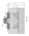
- a substrate 100 includes a crystalline semiconductor material.
- the substrate 100 may be, for example, a bulk silicon wafer, a bulk germanium wafer, a semiconductor-on-insulator (SOI) substrate, or a strained semiconductor-on-insulator (SSOI) substrate.
- a masking layer 110 is formed over the substrate 100 .
- the masking layer 110 may be an insulator layer including, for example, silicon dioxide, aluminum oxide, silicon nitride, silicon carbide, or diamond, and may have a thickness t 1 of, e.g., 50-1000 nanometers (nm).
- the masking layer 110 may be formed by a deposition method, such as chemical vapor deposition (CVD), plasma-enhanced chemical vapor deposition (PECVD), low pressure chemical vapor deposition (LPCVD), or a physical deposition method such as sputtering. Alternately, the masking layer 110 may be formed by thermal oxidation of the substrate.
- a mask (not shown), such as a photoresist mask, is formed over the masking layer 110 .
- the mask is patterned to expose at least a portion of the masking layer 110 .
- the exposed portion of the masking layer 110 is removed by, e.g., reactive ion etching (RIE) to define a window 120 to expose a region 130 of a top surface of the substrate 100 .
- the window 120 may have a width w 1 of, e.g., 50 nm-10 micrometers ( ⁇ m) and a length l 1 of, e.g., 50 nm-10 ⁇ m.
- the window has a height h 1 equal to the thickness t 1 of the masking layer 110 .
- the window 120 corresponds to the active area of the electronic or opto-electronic device into which it will eventually be incorporated, and the dimensions are selected accordingly.
- the window 120 is completely filled with an active area material 140 by selective epitaxy.
- Selective epitaxy may be performed by a deposition method such as LPCVD, atmospheric pressure CVD (APCVD), ultra-high vacuum CVD (UHCVD), reduced pressure CVD (RPCVD), metalorganic CVD (MOCVD), atomic layer deposition (ALD), or molecular beam epitaxy (MBE).
- the active area material 140 is formed selectively, i.e., it is formed on the crystalline semiconductor material of substrate 100 exposed by the window 120 , but is not substantially formed on the masking layer 110 .
- the active area material 140 is a crystalline semiconductor material, such as a group IV element or compound, a III-V compound, or a II-VI compound
- the group IV element may be carbon, germanium, or silicon, e.g., (110) silicon.
- the group IV compound may include silicon, germanium, tin, or carbon, e.g., silicon germanium (SiGe).
- the III-V compound may be, e.g., gallium arsenide (GaAs), indium arsenide (InAs), indium gallium arsenide (InGaAs), indium phosphide (InP), or indium antimonide (InSb), aluminum antimonide (AlSb), indium aluminum antimonide (InAlSb), or mixtures thereof.
- the II-VI compound may be, e.g., zinc telluride (ZnTe), cadmium selenide (CdSe), cadmium telluride (CdTe), zinc sulfide (ZnS), or zinc selenide (ZnSe), or mixtures thereof.
- more than one active area material 140 can be formed in window 120 , i.e., two or more layers of the active area material 140 can be formed by selective epitaxy. Defects may form at an interface between an active area material and the substrate 100 . These defects may be trapped by sidewalls of the masking layer 110 defining the window 120 , as described in U.S. patent application Ser. Nos. 11/436,198 and 11/436,062, incorporated herein by reference.
- a portion 150 of the active area material 140 may extend above a top surface 160 of the masking layer 110 for various reasons, thereby forming a non-planar top surface.
- facets may form at a vertical interface between the semiconductor active area material and the insulator.
- a top surface of the active area material 140 may not be co-planar with a top surface of the insulator material, because of the difficulty of stopping reliably and repeatably the selective epitaxy precisely at the point that the window 120 is filled with the active area material 140 .
- a non-planar surface may present subsequent processing difficulties.
- the portion of the active area material 140 extending above the masking layer 110 top surface may be removed by, for example, planarization, so that the active area material surface 170 is substantially coplanar with the top surface 160 of the masking layer 110 , as depicted in FIG. 1 c .
- the active area material surface may be planarized by, for example, a chemical-mechanical polishing (CMP) step that is selective with respect to the masking layer 110 .
- CMP chemical-mechanical polishing
- a device is formed including at least a portion of the active area material.
- the device may be a transistor 180 , with a source 190 , a drain 200 , and a channel 210 disposed in the active area material.
- Subsequent processing steps may include the formation of a gate dielectric layer 220 , the deposition of a gate electrode material, and the definition of a gate 230 by, e.g., dry etching.
- the source and drain regions may be defined by an ion implantation step.
- An interlayer dielectric may be formed over gate, source, and drain, and contact holes may be defined.
- a metal layer 235 may be deposited in the contact holes and over the structure.
- the resulting transistor 180 may be, for example, a field-effect transistor (FET), such as a complementary metal-oxide-semiconductor FET (CMOSFET) or a metal-semiconductor FET (MESFET).
- FET field-effect transistor
- CMOSFET complementary metal-oxide-semiconductor FET
- MESFET metal-semiconductor FET
- the device is a non-FET device such as a diode.
- the diode device could be a light detecting device (photodiode), or a light emitting device (either a light-emitting diode, or a laser diode).
- the device is a bipolar junction transistor.
- the active area material such as a III-V or II-VI semiconductor alloy, or Ge, or a SiGe alloy, may be introduced only into selected active areas on a wafer, as follows.
- a first shallow trench isolation (STI) region 300 is defined in semiconductor substrate 100 in accordance with methods known to one of skill in the art.
- the STI region 300 includes a trench 310 filled with a dielectric material 320 , such as silicon dioxide or silicon nitride.
- a thin dielectric layer 330 is formed over the substrate, including the first STI region.
- the thin dielectric layer 330 includes the same material as the dielectric material 320 .
- the thin dielectric layer 330 includes a material different from that of the dielectric material 320 .
- the thin dielectric layer 330 may include Si 3 N 4 and may have a thickness t 2 of, e.g., approximately 100-200 ⁇ .
- the thin dielectric layer 330 includes an SiO 2 layer disposed under the Si 3 N 4 layer.
- the SiO 2 layer alleviates the strain induced by the Si 3 N 4 layer, and the thickness t 2 of the Si 3 N 4 layer may be, for example, 1000 ⁇ .
- the thickness of the SiO 2 layer may be, for example, 100 ⁇ .
- a window 335 is defined in the thin dielectric layer 330 to expose a portion 340 of the substrate semiconductor material bound by the first STI region 300 , while protecting other substrate portions.
- the window 335 may be defined by, e.g., a photoresist mask and a wet or a dry etch chemistry that selectively removes a portion of the thin dielectric layer 330 without attacking the underlying substrate semiconductor material.
- the exposed semiconductor material portion 340 is removed to define an opening 350 .
- the semiconductor material portion 340 may be removed by a wet or dry etch chemistry that selectively removes the semiconductor material, e.g., Si, without attacking either the thin dielectric layer 330 or the STI trench fill material 320 .
- the semiconductor material portion 340 exposed by the window may be removed down to a level even with the bottom boundary of the first STI region 300 .
- the sidewalls 360 , 360 ′ of the opening 350 are defined by the dielectric material used to line and/or fill the first STI region 300 .
- Such a profile for opening 350 may be advantageous for avoidance of facet formation or for reduction of defects in materials subsequently deposited in opening 350 .
- the opening 350 is filled with active area material 140 by selective epitaxy.
- a top surface 370 of the active area material may be planarized such that the active area material is substantially coplanar with a top surface of the thin dielectric layer 330 .
- the planarization may be performed by a CMP step, stopping at the top surface of the thin dielectric layer 330 .
- more than one active area material 140 can be formed in window 335 , i.e., two or more layers of the active area material 140 can be formed by selective epitaxy.
- the thickness t 2 of the thin dielectric layer 330 may be small.
- An additional benefit of the small thickness t 2 is that the active area material extends only slightly above the semiconductor material of the substrate.
- the thin dielectric layer 330 is selectively removed, without substantially removing either the STI trench fill 320 or any underlying semiconductor material.
- the thin dielectric layer 330 may be effectively removed with a heated solution comprising phosphoric acid.
- a planarization step such as CMP, may be used to fully planarize the surface of the structure including the active area material, after the removal of the thin dielectric layer 330 , such that the active area material is substantially coplanar with the first STI region and the semiconductor material of the substrate.
- planarization after the removal of that layer may be preferable.
- a device such as a transistor, is defined, including at least a portion of the active area material 140 .
- the crystalline semiconductor material of the substrate may have a first crystalline orientation
- the active area material may include a second crystalline semiconductor material having a second crystalline orientation different from the first crystalline orientation.
- substrate 100 may include a first layer 400 having a first crystalline orientation
- a bonded layer 410 on the first layer 400 may include a second crystalline material having a second crystalline orientation, with a bonded interface 412 disposed between the two layers.
- the first crystalline material of the substrate and the second crystalline material may include the same material having different orientations.
- the first layer 400 may be (100) Si and the bonded layer may be (110) Si.
- substantially all of substrate 100 disposed below bonded layer 410 may consist of first layer 400 .
- first layer 400 may be a (100) Si wafer and bonded layer 410 may be (110) Si.
- first STI region 300 is defined in the bonded layer 410 , extending to the first layer 400 .
- first STI region 300 may extend into first layer 400 .
- the first STI region 300 bounds a portion 415 of the second crystalline semiconductor material.
- a masking overlayer 420 is defined over the substrate 100 .
- the masking overlayer 420 may be, for example, a thin low-stress Si 3 N 4 layer with a thickness t 3 of, e.g., approximately 100-200 ⁇ .
- a window 430 is defined in the masking overlayer 420 to expose the second crystalline semiconductor material portion 415 bound by the first STI region 300 .
- the exposed second crystalline semiconductor material may be removed by a dry or a wet etch to define an opening 440 .
- This removal can be via a non-selective wet or dry etch that is timed to stop after a surface 450 of the first layer 400 is exposed.
- this removal can be selective, via a wet etch that preferentially removes semiconductor material of a given crystalline orientation.
- TMAH tetramethyl-ammonium-hydroxide
- TMAH tetramethyl-ammonium-hydroxide
- the opening 440 is filled by the first crystalline material by selective epitaxy.
- a top surface of the selective epitaxial material 460 may be planarized such that it is substantially coplanar with the top surface of bonded layer 410 .
- the planarization may be performed by a CMP step, stopping, for example, at a top surface 470 of the masking overlayer 420 .
- the masking layer is removed, and devices are formed, having active areas comprising the first crystalline material and the second crystalline material, the two crystalline materials having different crystalline orientations.
- the active area 480 of an n-FET is bound by the first STI region 300
- the active area 490 of a p-FET is bound by a second STI region 300 ′ formed in parallel to the formation of the first STI region 300
- (110) surface Si has much higher hole mobility than the (100) surface, but the electron mobility of the (110) surface is poorer. It may be advantageous, therefore, to provide (100) Si in the area bound by the first STI region 300 for use as the active area 480 of an n-FET, and to provide (110) Si in the area 490 bound by the second STI region 300 ′ for use as the active area of a p-FET.
- the bonded layer 410 includes (100) Si and is bonded to a wafer including (110) Si. After the STI region 300 , 300 ′ formation, the (100) Si is removed from the area bound by the second STI region 300 ′. (110) Si is selectively grown in the area bound by the second STI region for use as the active area of a p-FET, and planarized. (100) Si bound by the first STI region is used as the active area of an n-FET.
- the bonded layer 410 is (100) strained silicon, transferred from a graded buffer on a second substrate and bonded to a (110) Si wafer. After STI formation, the (100) strained silicon is removed from the area bound by the second STI region 300 ′. (110) Si is selectively grown in the area bound by the second STI region 300 ′ for use as the active area of a p-FET, and planarized. (100) strained Si bound by the first STI region is used as the active area of an n-FET.
- an overlayer masking material such as masking overlayer 420 or thin dielectric layer 330 may be used to cover certain regions, e.g., p-FET regions, during the selective growth of alternative active area material on uncovered regions, e.g., n-FET regions.
- Defining the edge of the overlayer masking material is a challenge, because the lithographic step used to define the edge requires a very fine alignment to the STI region. For example, the alignment may need to be within ⁇ 10 nm. If the STI region to which the edge is aligned is too narrow in comparison to an alignment tolerance of the lithographic step, misalignment may result.
- the first STI region 300 that bounds a region in which an active area will be defined is wider than the second STI region 300 ′ formed on the same substrate 100 .
- STI region 300 may have a width w 2 selected from a range of 40 nm to 400 nm
- the second STI region 300 ′ may have a width w 3 selected from a range of 20 nm to 200 nm.
- a ratio of the width of STI region 300 to the width of the second STI region may be greater than 1, preferably selected from the range of 1.2 to 3. The ratio may also be greater than 3, but this may create an excessive area penalty.
- thin dielectric layer 330 is formed and a window is defined.
- the wider STI region 300 facilitates the alignment of the photoresist mask, such that edges 500 of the thin dielectric layer 330 are more reliably defined over the STI region 300 .
- the substrate semiconductor material 510 exposed by the window is removed to define an opening (not shown).
- the opening is filled with active area material 140 by selective epitaxy.
- a top surface of the active area material may be planarized such that the active area material is substantially coplanar with a top surface of the thin dielectric layer 330 . The planarization may be performed before and/or after the removal of the thin dielectric layer 330 .
- a first active area comprises the first active area material 140 and is bound by a first shallow trench isolation region 300 having a first width w 2 .
- a second active area comprises a second active area material 140 ′ and is bound by a second shallow trench isolation region 300 ′ having a second width w 3 .
- first STI region 300 that is wider than an active area is defined in substrate 100 comprising a crystalline semiconductor material.
- Thin dielectric layer 330 is formed over the substrate, and a window 600 is defined in the thin dielectric layer 330 to expose a portion of the first STI region 300 .
- the exposed portion of the first STI region is removed by, e.g., a dry etch which will not substantially etch silicon, comprising, e.g., HCl and/or HBr, to define an opening 610 .
- the opening 610 is filled with an active area material (not shown) by selective epitaxy.
- a top surface of the active area material may be planarized such that the active area material is substantially coplanar with a top surface of the thin dielectric layer 330 .
- the planarization may be performed before and/or after the removal of the thin dielectric layer 330 .
- more than one active area material can be formed in the opening 610 , i.e., two or more layers of the active area material can be formed by selective epitaxy.
- the remaining insulator strips 620 around the periphery of the opening will function as isolation structures.
- a ratio of the width of these strips to a width of a second STI region 300 ′ may be greater than 1.
- the thin dielectric layer is removed 330 , and a device is defined including at least a portion of the active area material.
- the first STI region 300 has a width w 4 of, e.g., the sum of the equivalent of the active area (typically a minimum of ten times the gate length) and two times a trench width (each typically two times a gate length). Thus, for a subsequently formed device with a gate length of 45 nm, the first STI region 300 may have a width of 630 nm.
- a masking layer 110 is formed over substrate 100 , which includes a crystalline material as described above.
- the masking layer 110 includes a non-crystalline material, such as a dielectric, e.g., SiO 2 or Si 3 N 4 .
- the masking layer 110 may act as an isolation region.
- a first opening 710 is defined in the first masking layer to expose a first portion of the substrate in a first region 720 of the substrate.
- the first opening 710 may be defined by a wet or a dry selective etch.
- the first opening is filled with a first active area material 730 by selective epitaxy, such that the first active area material forms in the first opening 710 , but is not substantially formed on the masking layer 110 .
- more than one active area material can be formed in the first opening 710 , i.e., two or more layers of the active area material can be formed by selective epitaxy.
- a second masking layer 740 may be formed over the substrate such that the first region of the substrate is covered.
- the second masking layer 740 includes a non-crystalline material, such as a dielectric.
- a second opening 750 is defined in the second and first masking layer to expose a second portion of the substrate in a second region 760 of the substrate.
- the second opening is filled with a second active area material 770 by selective epitaxy.
- the second masking layer 740 prevents the second active area material 770 from forming by selective epitaxy on the crystalline first active area material 730 .
- the second masking layer may be removed by, e.g., a selective wet etch, after the second opening is filled with the second active area material.
- more than one active area material can be formed in the second opening 750 , i.e., two or more layers of the active area material can be formed by selective epitaxy.
- the structure may include first isolation region 110 ′, first active area comprising a first active area material 730 and bound by the first isolation region 110 ′, second isolation region 110 ′′, and second active area comprising a second active area material 770 different from the first active area material and bound by the second isolation region 110 ′′.
- a surface of the first active area material 730 , a surface of the second active area material 770 , a surface of the first isolation region 110 ′, and a surface of the second isolation region 110 ′′ are all substantially coplanar.
- Each of the first and second active area materials 730 , 770 may be formed in the manner discussed above with respect to active area material 140 , and may include any of the listed materials.
- the first active area material has a first crystalline orientation and the second active area material has a second crystalline orientation different from the first crystalline orientation.
- the first active area material may include at least one of a group IV element or compound, such as Si or Ge or SiGe, or a III-V compound, such as InAs, InGaAs, InSb, AlSb, InAlSb, GaAs, and InP
- the second active area material may include at least one of a group IV element or compound, such as Si or Ge or SiGe, or a III-V compound, such as InAs, InGaAs, InSb, AlSb, InAlSb, GaAs, and InP.
- a surface of the first active area material and a surface of the second active area material may be planarized by, e.g., CMP.
- This CMP step enables the non-selective polishing of two different materials by polishing both the first active area material and the second active area material at the same rate.
- a first device including the first active area is formed, and a second device including the second active area is formed.
- a first active area material may be suitable for use as the active area of an n-FET, e.g., InGaAs
- the second active area material may be suitable for use as the active area of a p-FET, e.g., Si, Ge, or SiGe.
- no second masking layer 740 is formed prior to the formation of the second active area material.
- the second opening 750 in the first masking layer 110 is defined and filled with the second active area material 770 .
- the second active area material 770 is formed by selective epitaxy, which results in the second active area material being formed on all exposed crystalline surfaces, including a top surface of the first active area material.
- the structure may be planarized by, e.g., CMP.
- CMOS circuit may have different active area materials.
- the design and processing challenges of the incorporation of two types of active area materials in a single substrate may be reduced by the use of a single source/drain material for both n- and p-FET.
- the described structure allows a CMOS circuit to include an n-FET with a channel having a first type of stress and a p-FET with a channel having a second type of stress, which may be beneficial for various channel material combinations.
- a CMOS device 900 may include (i) a n-FET 905 that has a first channel 910 disposed in a first active area material 915 , such as Ge, GaAs, InAs, InSb, or InGaAs, a first source region 920 , and a first drain region 925 ; and (ii) an p-FET 930 may have a second channel 940 disposed in a second active area material 935 , such as SiGe, Ge, Si with a (110) surface, or InSb, a second source region 945 , and a second drain region 950 .
- the CMOS device 900 may be formed as follows.
- the first active area material 915 suitable for use as first channel 910 of the n-FET 905 , is provided in a first region 955 of semiconductor substrate 100 .
- the second active area material 935 suitable for use as second channel 940 of the p-FET 930 , is provided in a second region 960 of semiconductor substrate 100 .
- the first source and the first drain regions 920 , 925 are defined by first defining a first and a second recess 965 , 970 by removing a first portion and a second portion of the first active area material 915 , and then depositing a source/drain material into the first and second recesses.
- the second source and the second drain regions 945 , 950 are defined by first defining a third and a fourth recess 980 , 985 by removing a first portion and a second portion of the second active area material 935 , and then depositing a source/drain material into the third and fourth recesses.
- the recesses may be formed by a suitable wet or dry etch.
- the first, second, third, and fourth recesses 965 , 970 , 980 , 985 may be formed by a non-selective etch that removes the first and second active area materials at approximately the same rate.
- a dry etch with a 45% SF 6 /55% O 2 chemistry [with total gas pressure of 100 milliTorr (mTorr), RF power of 50 Watts, and total gas flow rate of 30 standard cubic centimeters per minute (sccm)] may be used to etch active areas that include Si and Ge at approximately the same rate of 200 nm/min. (See A.
- first and second recesses 965 , 970 in the first active material may be defined by an etch that is highly selective with respect to the second active material.
- the third and fourth recesses 980 , 985 may be removed by an etch that is highly selective with respect to the first active material.
- the first and second recesses 965 , 970 in the Si material may be created with a SF 6 /H 2 /CF 4 etch chemistry.
- Gas flows of 35 sccm for SF 6 , 65 sccm for H 2 , and 80 sccm for CF 4 , a pressure of 150 mTorr and RF power of 50 Watts enable this chemistry to etch Si at approximately 10 nm/min with complete selectivity to Ge.
- the third and fourth recesses 980 , 985 may then be created with an HCl etch chemistry, at a total pressure of 20 Torr and an HCl partial pressure of 208 mTorr (in H 2 carrier gas). At an etch temperature of 500-600° C., this chemistry etches Ge at 10-20 nm/min with complete selectivity to Si.
- HCl etch chemistry at a total pressure of 20 Torr and an HCl partial pressure of 208 mTorr (in H 2 carrier gas).
- this chemistry etches Ge at 10-20 nm/min with complete selectivity to Si.
- the source/drain material deposited into the first source and drain regions 920 , 925 is the same as the source/drain material deposited into the second source and drain regions 945 , 950 .
- desired types of stress may be induced in the active area materials.
- the first active area material may be under tensile strain
- the second active area material may be under compressive strain.
- the channel 940 of the p-FET 930 is compressively strained and the channel 910 of the n-FET 905 is tensilely strained; thus, for the case of channel materials comprising, for example, Si, SiGe, or Ge the carrier mobilities of both devices are enhanced.
- the source/drain material has a lattice constant that is smaller than a lattice constant of the first active area material of the n-FET channel.
- the n-FET channel is tensilely strained.
- the lattice constant of the source/drain material is larger than a lattice constant of the second active area material of the p-FET channel.
- the p-FET channel is compressively strained.
- the first active area material may be Ge
- the second active area material may be Si
- the source/drain material may be SiGe.
- the first active area material may be under compressive strain, and/or the second active area material may be under tensile strain. Therefore, the channel 940 of the p-FET 930 is tensilely strained and the channel 910 of the n-FET 905 is compressively strained.
- the source/drain material has a lattice constant that is larger than a lattice constant of the first active area material of the n-FET channel. Hence, the n-FET channel 910 is compressively strained.
- the lattice constant of the source/drain material is smaller than a lattice constant of the second active area material of the p-FET channel 940 .
- the p-FET channel 940 is tensilely strained. More particularly, the first active area material may be Si, the second active area material may be Ge, and the source/drain material may be SiGe.
- the type of strain that may be beneficial for device performance may be determined from piezoresistance coefficients.
- a relatively large positive piezoresistance coefficient is an indicator that compressive strain will enhance carrier mobilities.
- a relatively large negative piezoresistance coefficient is an indicator that tensile strain will enhance carrier mobilities.
- the piezoresistance coefficient for ⁇ 110> Si for p-type devices is 71.8, as measured in parallel to current flow.
- compressive strain will help increase carrier mobilities in p-type devices having ⁇ 110>-oriented Si channels.
- the piezoresistance coefficient for ⁇ 110> Ge for n-type devices is ⁇ 72, as measured in parallel to current flow.
- CMOS device 900 includes n-FET 905 having a ⁇ 110>-oriented Ge tensilely strained channel 910 , and p-FET 930 with a ⁇ 110>-oriented Si compressively strained channel 940 , and a source/drain material of Si x Ge y .
- At least a portion of the source/drain material in the first source and first drain regions 920 , 925 is disposed in a first and a second recess 965 , 970
- at least a portion of the source/drain material in the second source and second drain regions 945 , 950 is disposed in a third and a fourth recess 980 , 985
- a lattice constant of the source/drain material is smaller than a lattice constant of the first active area material 915 and larger than a lattice constant of the second active area material 935
- a lattice constant of the source/drain material is larger than a lattice constant of the first active area material 915 and smaller than a lattice constant of the second active area material 935 .
- the source/drain material in the first source and first drain regions 920 , 925 is disposed in a first and a second recess 965 , 970
- the source/drain material in the second source and second drain regions 945 , 950 is disposed on a top surface of the second active area material
- a lattice constant of the source/drain material is smaller than a lattice constant of the first active area material 915 and smaller than a lattice constant of the second active area material 935 .
- third and fourth recesses 980 , 985 are not formed before deposition of the source/drain material because additional strain on p-FET 930 is not desired or may even deleteriously affect performance of p-FET 930 .
- the source/drain material may include a group IV semiconductor, such as Si, Ge, SiGe, or SiC.
- the source/drain material in the first source and first drain regions 920 , 925 is disposed on a top surface of the first active area material, at least a portion of the source/drain material in the second source and second drain regions 945 , 950 is disposed in a third and a fourth recess 980 , 985 , and a lattice constant of the source/drain material is larger than a lattice constant of the first active area material 915 and larger than a lattice constant of the second active area material 935 .
- first and second recesses 965 , 970 are not formed before deposition of the source/drain material because additional strain on n-FET 905 is not desired or may even deleteriously affect performance of n-FET 905 .
- a first device such as n-FET 905
- a second device such as a p-FET 930
- a channel 940 disposed in the second active area material between the second source 945 and the second drain 950 .
- CMOS devices having different n- and p-active areas may be simplified by the use of a single gate dielectric material for both n- and p-type devices.
- first active area material 730 is provided over a first portion 1000 of substrate 100
- second active area material 770 is provided over a second portion 1010 of substrate 100 , as discussed above with reference to FIGS. 7 a - 7 e .
- the first and second active area materials may each include, for example, at least one of Ge, SiGe, SiC, diamond, III-V semiconductors, and II-VI semiconductors.
- This deposition may be selective, i.e., such that deposition occurs on the active area materials, but not on the surface of the isolation regions surrounding the active areas.
- This thin layer 1020 may include, e.g., Si, Ge, or another material selected for its high quality interface properties with a particular gate dielectric.
- This thin layer 1020 may be deposited by, e.g., a method such as ALD, that allows for very fine thickness control.
- a gate dielectric layer 1030 is thereafter formed over the thin layer 1020 .
- the thin layer 1020 includes Si and the gate dielectric layer 1030 includes thermally grown SiO 2 .
- the gate dielectric layer 1030 may include SiON, Si 3 N 4 , or a deposited high-k dielectric, such as hafnium oxide (HfO 2 ), aluminum oxide (Al 2 O 3 ), or zirconium oxide (ZrO 2 ).
- a first device 1040 is formed including the first active area material 730 and a second device 1050 is formed including the second active area material 770 .
- the first device 1040 may be an n-FET and the second device 1050 may be a p-FET.
- CMOS devices having different n- and p-active areas may be improved by the use of different gate electrode materials for the n- and p-type devices, selected, e.g., in view of work-function considerations.
- first active area material 730 is provided over a first portion 720 of substrate 100
- second active area material 770 is provided over a second portion 760 of substrate 100 , as discussed above with reference to FIGS. 7 a - 7 e .
- Gate dielectric layer 1030 is formed over the substrate 100 , either directly over both of the first and second active areas, or by first forming the thin layer 1020 as described above with reference to FIGS. 10 a - 10 c .
- a first gate dielectric layer is formed over the first active area material 730 and a second gate dielectric layer is formed over the second active area material 770 .
- the second active area material may be masked by a dielectric masking layer such as SiO 2 or Si 3 N 4 , and the first gate dielectric layer is formed over only exposed first active area material 730 by a method such as oxidation, nitridation, or atomic layer deposition.
- the masking material may be removed from the second active area and applied to the first active area.
- the second gate dielectric layer may then be formed over only exposed second active area material 770 by a method such as oxidation, nitridation, or atomic layer deposition.
- the masking material may then be removed.
- the first and second gate dielectric layers are formed from the same material and are formed in a single step.
- a first gate electrode material 1100 is deposited over the substrate 100 , including over the first active area material 730 .
- the first gate electrode material 1100 may be suitable for use as a gate of an n-FET device, and may include, for example, indium (In), tantalum (Ta), zirconium (Zr), tungsten (W), molybdenum (Mo), chromium (Cr), tin (Sn), zinc (Zn), cobalt (Co), nickel (Ni), rhenium (Re), ruthenium (Ru), platinum (Pt), titanium (Ti), hafnium (Hf), alloys of one or more of the aforementioned materials, and alloys of one or more of the aforementioned materials with Si and/or nitrogen.
- the first gate electrode material 1100 disposed over the second active area material 770 may be removed, e.g., by a wet or dry etch highly selective to the underlying gate dielectric layer.
- a suitable dry etch may be XeF 2 at 2.6 mTorr, which will etch Ti, Ta, Mo, and W but is very selective to most oxides. (See K. R. Williams, et al., “Etch Rates for Micromachining Processing-Part II,” J. Micromechanical Systems , Vol. 12, No. 6, p. 761, 2003, incorporated herein by reference.)
- a second gate electrode material 1110 is deposited over the substrate 100 , including over the second active area material 770 .
- the second gate electrode material 1110 may be suitable for use as a gate of a p-FET device, and may include, for example, copper (Cu), Mo, Cr, W, Ru, Ta, Zr, Pt, Hf, Ti, Co, Ni, alloys of one or more of the aforementioned materials, and alloys of one or more of the aforementioned materials with Si and/or nitrogen.
- the second gate electrode material 1110 disposed over the first active area material 730 may be removed, e.g., by a wet or dry etch highly selective to the underlying first gate electrode material.
- a room-temperature wet etch solution of 10:1 H 2 O:HF can be used to remove the Ti at a rate of approximately 1100 nm/minute, while stopping selectively on the W that is etched at a rate at least 100 times slower.
- the second gate electrode material 1110 disposed over the first active area material 730 may be removed by a planarization step, such as CMP.
- the first and second gate electrode layers 1100 , 1110 disposed over the substrate 100 are planarized to define a co-planar surface 1130 including a surface of the first electrode layer 1100 disposed over the first active area material 730 and a surface of the second electrode layer 1110 disposed over the second active area material 770 .
- the first gate electrode material 1100 may be used as a CMP stop for the second gate electrode material.
- a first gate may be defined over the first active area material and a second gate may be defined over the second active area material.
- a first device, such as an n-FET is defined, including the first active area material, and a second device, such as a p-FET is defined, including the second active area material.
- two different materials may be deposited in a single active area region to improve device characteristics.
- certain channel materials e.g., InSb or InAs
- a transistor 1200 having an active area including a channel material with a relatively low band gap may be susceptible to high source and/or drain 1202 , 1204 leakage. Improved results may be achieved by defining an active area by the selective epitaxy of two active area materials.
- a bi-layer structure is defined by the selective epitaxy of a lower active area material layer 1210 in a window 120 defined in the masking layer 110 .
- the lower active area material layer 1210 may include a first semiconductor material 1215 (S 1 ) having a relatively high band gap, such as GaSb, AlSb, CdSe, ZnTe, InAlAs, CdTe, or InAlSb.
- a thickness t 4 of the first active area material 1210 may be equal to depth d 1 of the window 120 .
- Thickness t 4 and depth d 1 may be, for example, selected from a range of, e.g., 200 nm to 500 nm.
- a planarization step e.g., CMP to planarize lower active area material layer 1210 may be performed, so that the top surface of lower active area material layer 1210 and the top surface of masking layer 110 are co-planar.
- an upper active area material layer 1220 may be formed over the lower active area material layer 1210 .
- the upper active area material layer may include a second semiconductor material 1225 (S 2 ) that provides a high carrier mobility, but may have a low bandgap, such as InAs or InSb.
- a thickness t 5 of the upper active material layer may be, for example, selected from a range of 5 nm to 100 nm.
- the lower active area material may be substantially uniform, e.g., ungraded, in composition.
- a lattice mismatch between the first material S 1 1215 and the second material S 2 1225 is sufficiently small to reduce the formation of defects.
- the lattice mismatch is preferably less than about 2%.
- a device 1250 such as a transistor, may be formed including the lower and upper active area layers 1210 , 1220 . Bottom portions of source and drain regions 1260 , 1265 may be disposed in the lower active area layer 1210 , and upper portions of the source and drain regions 1260 , 1265 may be disposed in the upper active area layer 1220 . Leakage current is thereby reduced while high carrier mobility is provided.
- Defects 1230 may form at an interface between the substrate and the semiconducting material S 1 , due to lattice constant mismatch. These defects may be trapped by sidewalls of the masking layer 110 defining the window 120 , as described in U.S. patent application Ser. Nos. 11/436,198 and 11/436,062,
- selective epitaxy of active area materials may be used to provide channel regions with high strain levels, e.g., ⁇ 1.5%, that may be used in both NMOS and PMOS devices.
- Masking layer 110 is formed over substrate 100 , which includes a crystalline material as described above.
- the masking layer 110 includes a non-crystalline material, such as a dielectric, e.g., SiO 2 or Si 3 N 4 .
- First opening 710 is defined in the masking layer 110 , exposing a first portion 1300 of the substrate 100 .
- First active area material 730 such as Si, is grown by selective epitaxy within the first opening 710 .
- a top portion of the first active area material 730 extending above a top surface of the masking layer 110 may be planarized by, e.g., CMP. Thereafter, a first layer 1310 including second active area material 770 is selectively grown over the first active area material 730 .
- the second active area material 770 may be lattice mismatched to the first active area material 730 .
- Si 1-x Ge x may be formed over relaxed Si, with x ⁇ 0.35.
- a thickness t 6 of the second active area material 770 is preferably less than a thickness leading to gross relaxation.
- this relaxation thickness is approximately three to four times a critical thickness h c , i.e., a thickness at which misfit dislocations may start to appear.
- a critical thickness at which misfit dislocations may start to appear is approximately 65 nm, so thickness t 6 is preferably less than approximately 260 nm.
- first and second active area materials 730 , 770 may be formed in the manner discussed above with respect to active area material 140 , and may include any of the listed materials.
- the first active area material may include at least one of a group IV element or compound, such as Si or Ge or SiGe, or a III-V compound, such as InAs, InGaAs, InSb, AlSb, InAlSb, GaAs, and InP
- the second active area material may include at least one of a group IV element or compound, such as Si or Ge or SiGe, or a III-V compound, such as InAs, InGaAs, InSb, AlSb, InAlSb, GaAs, and InP.
- the second masking layer 740 includes a non-crystalline material, such as a dielectric, e.g., SiO 2 or Si 3 N 4 .
- Second opening 750 is defined in the masking layer 110 .
- the second opening 750 is filled with a third active area material 1315 , e.g., Si 1-x Ge x with x ⁇ 0.35.
- a thickness of the third active area material 1315 is preferably greater than a thickness that leads to gross relaxation, such that the third active area material is relaxed.
- this relaxation thickness is approximately three to four times a critical thickness h c , i.e., a thickness at which misfit dislocations may start to appear.
- a critical thickness at which misfit dislocations may start to appear is approximately 65 nm, so the thickness of the third active material 1315 is preferably greater than approximately 260 nm.
- Defects may form at an interface between the second active area material 770 and the substrate 100 . These defects may be trapped by sidewalls of the masking material 110 defining the opening 750 , as described in U.S. patent application Ser. Nos. 11/436,198 and 11/436,062.
- a top portion of the third active area material 1315 extending above the top surface of the masking layer 110 may be planarized by, e.g., CMP. Thereafter, a second layer 1320 comprising a fourth active area material 1317 , e.g., Si, is selectively grown over the third active area material 1315 .
- a thickness t 7 of the fourth active area material 1317 is preferably less than a thickness that leads to gross relaxation. For tensilely strained layers, such as Si disposed over relaxed Si 1-x Ge x , the thickness t 7 is less than about 10 times the critical thickness h c .
- the critical thickness at which misfit dislocations may start to appear is approximately 65 nm, so thickness t 7 is preferably less than approximately 650 nm.
- the second masking layer 740 is removed by, e.g., a selective wet etch.
- Each of the third and fourth active area materials 1315 , 1317 may be formed in the manner discussed above with respect to active area material 140 , and may include any of the listed materials.
- the third active area material may include at least one of a group IV element or compound, such as Si or Ge or SiGe, or a III-V compound, such as InAs, InGaAs, InSb, AlSb, InAlSb, GaAs, and InP
- the fourth active area material may include at least one of a group IV element or compound, such as Si or Ge or SiGe, or a III-V compound, such as InAs, InGaAs, InSb, AlSb, InAlSb, GaAs, and InP.
- the first and second active area materials 730 , 770 deposited in the first opening 710 may be the same as the fourth and third active area materials 1317 , 1315 , respectively, deposited in the second opening 750 .
- This will result in equivalent strain levels for, e.g., NMOS and PMOS devices incorporating these active areas. That is, an NMOS and a PMOS device will incorporate strains substantially identical in magnitude but opposite in sign.
- Si on SiGe is used for the NMOS regions, and SiGe on Si is used for the PMOS regions, thus providing the beneficial sign of strain for both NMOS and PMOS regions.
- Other combinations of materials are possible.
- a guideline for material selection may be that for the NMOS case the natural lattice constant of the channel material is preferably smaller than the semiconductor below, and vice versa for PMOS.
- the lower active area material is substantially relaxed, such that the upper active area material is strained.
- a resulting structure 1355 includes first and second active areas 1360 , 1370 .
- the first active area 1360 may be suitable for formation of a PMOS device. It may include second active area material 770 , e.g., highly compressively strained Si 1-x Ge x , disposed over first active area material 730 , e.g., Si. The highly compressively strained material may enhance PMOS device performance by providing high hole mobility.
- the second active area 1370 may be suitable for formation of an NMOS device. It may include fourth active area material 1317 , e.g., highly tensilely strained Si, disposed over third active area material 1315 , e.g., relaxed Si 1-x Ge x . The highly tensilely strained material may enhance NMOS device performance by providing high electron mobility.
- PMOS and NMOS transistors 1380 , 1385 are formed over first and second active areas 1360 , 1370 of the structure 1355 .
- the PMOS and NMOS transistors may have shallow source and drain regions 1390 , 1390 ′, 1395 , 1395 ′ disposed entirely in the upper active area materials, i.e., second active area material 770 and fourth active area material 1317 , respectively.
- the source and drain regions do not intersect an interface between two epitaxial layers, that may include misfit dislocations that may lead to severe, unacceptable leakage.
- the source and drain regions 1390 , 1390 ′, 1395 , 1395 ′ may include silicide material, thereby enhancing source and drain contacts.
- the source and drain regions may be thickened by selective epitaxy.
- the PMOS source and drain regions may include Si 1-x Ge x and the NMOS source and drain regions may include Si, thereby enhancing the respective device performances.
- a non-uniform doping profile may be formed during the epitaxy of the layers. This doping profile may preferably have a lower concentration of dopants in a top portion of the layer(s).
Landscapes
- Metal-Oxide And Bipolar Metal-Oxide Semiconductor Integrated Circuits (AREA)
- Insulated Gate Type Field-Effect Transistor (AREA)
- Recrystallisation Techniques (AREA)
- Thin Film Transistor (AREA)
- Element Separation (AREA)
Abstract
Description
| TABLE 1 |
| S1 and S2 material combinations |
| S2 | S1 | S1 Eg (eV) | ||
| InAs | GaSb | 0.8 | ||
| InAs | AlSb | 1.7 | ||
| InAs | CdSe | 1.8 | ||
| InAs | ZnTe | 2.4 | ||
| InAs | InAlAs | 0.8-1.0 | ||
| InSb | CdTe | 1.5 | ||
| InSb | InAlSb | 0.8 | ||
Claims (14)
Priority Applications (1)
| Application Number | Priority Date | Filing Date | Title |
|---|---|---|---|
| US11/493,365 US7626246B2 (en) | 2005-07-26 | 2006-07-26 | Solutions for integrated circuit integration of alternative active area materials |
Applications Claiming Priority (2)
| Application Number | Priority Date | Filing Date | Title |
|---|---|---|---|
| US70236305P | 2005-07-26 | 2005-07-26 | |
| US11/493,365 US7626246B2 (en) | 2005-07-26 | 2006-07-26 | Solutions for integrated circuit integration of alternative active area materials |
Publications (2)
| Publication Number | Publication Date |
|---|---|
| US20070181977A1 US20070181977A1 (en) | 2007-08-09 |
| US7626246B2 true US7626246B2 (en) | 2009-12-01 |
Family
ID=37573678
Family Applications (1)
| Application Number | Title | Priority Date | Filing Date |
|---|---|---|---|
| US11/493,365 Active 2026-10-01 US7626246B2 (en) | 2005-07-26 | 2006-07-26 | Solutions for integrated circuit integration of alternative active area materials |
Country Status (6)
| Country | Link |
|---|---|
| US (1) | US7626246B2 (en) |
| EP (1) | EP1911086A2 (en) |
| JP (1) | JP5481067B2 (en) |
| KR (1) | KR101329388B1 (en) |
| CN (1) | CN101268547B (en) |
| WO (1) | WO2007014294A2 (en) |
Cited By (42)
| Publication number | Priority date | Publication date | Assignee | Title |
|---|---|---|---|---|
| US20080254635A1 (en) * | 2005-09-30 | 2008-10-16 | Hubert Benzel | Method for Accelerated Etching of Silicon |
| US20090261346A1 (en) * | 2008-04-16 | 2009-10-22 | Ding-Yuan Chen | Integrating CMOS and Optical Devices on a Same Chip |
| US20100025683A1 (en) * | 2008-07-01 | 2010-02-04 | Amberwave Systems Corporation | Reduction of edge effects from aspect ration trapping |
| US20110086491A1 (en) * | 2009-10-08 | 2011-04-14 | Taiwan Semiconductor Manufacturing Company, Ltd. | Growing a III-V Layer on Silicon using Aligned Nano-Scale Patterns |
| US20110147703A1 (en) * | 2009-12-17 | 2011-06-23 | Lehigh University | ABBREVIATED EPITAXIAL GROWTH MODE (AGM) METHOD FOR REDUCING COST AND IMPROVING QUALITY OF LEDs AND LASERS |
| US20110180806A1 (en) * | 2010-01-28 | 2011-07-28 | Intersil Americas Inc. | Monolithic integration of gallium nitride and silicon devices and circuits, structure and method |
| US8053304B2 (en) * | 2009-02-24 | 2011-11-08 | Taiwan Semiconductor Manufacturing Company, Ltd. | Method of forming high-mobility devices including epitaxially growing a semiconductor layer on a dislocation-blocking layer in a recess formed in a semiconductor substrate |
| US20120025201A1 (en) * | 2010-07-30 | 2012-02-02 | Taiwan Semiconductor Manufacturing Company, Ltd. | Inverted Trapezoidal Recess for Epitaxial Growth |
| US20120040512A1 (en) * | 2010-08-11 | 2012-02-16 | Globalfoundries | Method to form nanopore array |
| US20120168823A1 (en) * | 2010-12-31 | 2012-07-05 | Zhijiong Luo | Semiconductor device and method for manufacturing the same |
| US8216951B2 (en) | 2006-09-27 | 2012-07-10 | Taiwan Semiconductor Manufacturing Company, Ltd. | Quantum tunneling devices and circuits with lattice-mismatched semiconductor structures |
| US8237151B2 (en) | 2009-01-09 | 2012-08-07 | Taiwan Semiconductor Manufacturing Company, Ltd. | Diode-based devices and methods for making the same |
| US8253211B2 (en) | 2008-09-24 | 2012-08-28 | Taiwan Semiconductor Manufacturing Company, Ltd. | Semiconductor sensor structures with reduced dislocation defect densities |
| US20120267688A1 (en) * | 2009-12-15 | 2012-10-25 | Sumitomo Chemical Company, Limited | Semiconductor wafer, semiconductor device, and method for producing semiconductor wafer |
| US8304805B2 (en) | 2009-01-09 | 2012-11-06 | Taiwan Semiconductor Manufacturing Company, Ltd. | Semiconductor diodes fabricated by aspect ratio trapping with coalesced films |
| US8324660B2 (en) | 2005-05-17 | 2012-12-04 | Taiwan Semiconductor Manufacturing Company, Ltd. | Lattice-mismatched semiconductor structures with reduced dislocation defect densities and related methods for device fabrication |
| US8329541B2 (en) | 2007-06-15 | 2012-12-11 | Taiwan Semiconductor Manufacturing Company, Ltd. | InP-based transistor fabrication |
| US8344242B2 (en) | 2007-09-07 | 2013-01-01 | Taiwan Semiconductor Manufacturing Company, Ltd. | Multi-junction solar cells |
| US8384196B2 (en) | 2008-09-19 | 2013-02-26 | Taiwan Semiconductor Manufacturing Company, Ltd. | Formation of devices by epitaxial layer overgrowth |
| US20130146893A1 (en) * | 2010-09-14 | 2013-06-13 | Taiwan Semiconductor Manufacturing Company, Ltd. | Sic crystalline on si substrates to allow integration of gan and si electronics |
| US20130171792A1 (en) * | 2011-12-28 | 2013-07-04 | Taiwan Semiconductor Manufacturing Company, Ltd. | Methods for Semiconductor Regrowth |
| US8502263B2 (en) | 2006-10-19 | 2013-08-06 | Taiwan Semiconductor Manufacturing Company, Ltd. | Light-emitter-based devices with lattice-mismatched semiconductor structures |
| US8535544B2 (en) | 2010-07-26 | 2013-09-17 | International Business Machines Corporation | Structure and method to form nanopore |
| US8624103B2 (en) | 2007-04-09 | 2014-01-07 | Taiwan Semiconductor Manufacturing Company, Ltd. | Nitride-based multi-junction solar cell modules and methods for making the same |
| US8629446B2 (en) | 2009-04-02 | 2014-01-14 | Taiwan Semiconductor Manufacturing Company, Ltd. | Devices formed from a non-polar plane of a crystalline material and method of making the same |
| US8822248B2 (en) | 2008-06-03 | 2014-09-02 | Taiwan Semiconductor Manufacturing Company, Ltd. | Epitaxial growth of crystalline material |
| US8847279B2 (en) | 2006-09-07 | 2014-09-30 | Taiwan Semiconductor Manufacturing Company, Ltd. | Defect reduction using aspect ratio trapping |
| US8853035B2 (en) | 2011-10-05 | 2014-10-07 | International Business Machines Corporation | Tucked active region without dummy poly for performance boost and variation reduction |
| US8878243B2 (en) | 2006-03-24 | 2014-11-04 | Taiwan Semiconductor Manufacturing Company, Ltd. | Lattice-mismatched semiconductor structures and related methods for device fabrication |
| US8981427B2 (en) | 2008-07-15 | 2015-03-17 | Taiwan Semiconductor Manufacturing Company, Ltd. | Polishing of small composite semiconductor materials |
| WO2015076956A1 (en) * | 2013-11-25 | 2015-05-28 | Qualcomm Incorporated | Complementarily strained finfet structure |
| US20150179664A1 (en) * | 2013-12-24 | 2015-06-25 | Alejandro X. Levander | Heterogeneous semiconductor material integration techniques |
| US9228994B1 (en) | 2014-08-06 | 2016-01-05 | Globalfoundries Inc. | Nanochannel electrode devices |
| US9508890B2 (en) | 2007-04-09 | 2016-11-29 | Taiwan Semiconductor Manufacturing Company, Ltd. | Photovoltaics on silicon |
| US9859381B2 (en) | 2005-05-17 | 2018-01-02 | Taiwan Semiconductor Manufacturing Company, Ltd. | Lattice-mismatched semiconductor structures with reduced dislocation defect densities and related methods for device fabrication |
| US9984872B2 (en) | 2008-09-19 | 2018-05-29 | Taiwan Semiconductor Manufacturing Company, Ltd. | Fabrication and structures of crystalline material |
| US20180308845A1 (en) * | 2016-02-24 | 2018-10-25 | International Business Machines Corporation | Patterned gate dielectrics for iii-v-based cmos circuits |
| US10453757B2 (en) | 2013-03-13 | 2019-10-22 | Taiwan Semiconductor Manufacturing Company, Ltd. | Transistor channel |
| US10504799B2 (en) | 2016-02-24 | 2019-12-10 | International Business Machines Corporation | Distinct gate stacks for III-V-based CMOS circuits comprising a channel cap |
| KR20200072985A (en) * | 2018-12-13 | 2020-06-23 | 삼성전자주식회사 | An integrated circuit including a plurality of transistors and a method of manufacturing the same |
| US11342442B2 (en) | 2012-07-17 | 2022-05-24 | Unm Rainforest Innovations | Semiconductor product comprising a heteroepitaxial layer grown on a seed area of a nanostructured pedestal |
| US20240222366A1 (en) * | 2020-10-16 | 2024-07-04 | Globalfoundries U.S. Inc. | Device integration schemes leveraging a bulk semiconductor substrate having a <111> crystal orientation |
Families Citing this family (62)
| Publication number | Priority date | Publication date | Assignee | Title |
|---|---|---|---|---|
| US20070054467A1 (en) * | 2005-09-07 | 2007-03-08 | Amberwave Systems Corporation | Methods for integrating lattice-mismatched semiconductor structure on insulators |
| US7638842B2 (en) | 2005-09-07 | 2009-12-29 | Amberwave Systems Corporation | Lattice-mismatched semiconductor structures on insulators |
| US20070252216A1 (en) * | 2006-04-28 | 2007-11-01 | Infineon Technologies Ag | Semiconductor device and a method of manufacturing such a semiconductor device |
| US7636610B2 (en) * | 2006-07-19 | 2009-12-22 | Envisiontec Gmbh | Method and device for producing a three-dimensional object, and computer and data carrier useful therefor |
| JP2008060408A (en) * | 2006-08-31 | 2008-03-13 | Toshiba Corp | Semiconductor device |
| WO2008039495A1 (en) | 2006-09-27 | 2008-04-03 | Amberwave Systems Corporation | Tri-gate field-effect transistors formed by aspect ratio trapping |
| US8377812B2 (en) * | 2006-11-06 | 2013-02-19 | General Electric Company | SiC MOSFETs and self-aligned fabrication methods thereof |
| US20080108190A1 (en) * | 2006-11-06 | 2008-05-08 | General Electric Company | SiC MOSFETs and self-aligned fabrication methods thereof |
| KR100850859B1 (en) * | 2006-12-21 | 2008-08-06 | 동부일렉트로닉스 주식회사 | Image Sensor and The Fabricating Method thereof |
| US7466008B2 (en) * | 2007-03-13 | 2008-12-16 | Taiwan Semiconductor Manufacturing Company, Ltd. | BiCMOS performance enhancement by mechanical uniaxial strain and methods of manufacture |
| US7598142B2 (en) * | 2007-03-15 | 2009-10-06 | Pushkar Ranade | CMOS device with dual-epi channels and self-aligned contacts |
| JP2008227432A (en) * | 2007-03-16 | 2008-09-25 | Furukawa Electric Co Ltd:The | Nitride compound semiconductor device and manufacturing method thereof |
| US20080242062A1 (en) * | 2007-03-31 | 2008-10-02 | Lucent Technologies Inc. | Fabrication of diverse structures on a common substrate through the use of non-selective area growth techniques |
| US7906381B2 (en) | 2007-07-05 | 2011-03-15 | Stmicroelectronics S.A. | Method for integrating silicon-on-nothing devices with standard CMOS devices |
| FR2918793B1 (en) * | 2007-07-11 | 2009-10-09 | Commissariat Energie Atomique | PROCESS FOR PRODUCING A SEMICONDUCTOR-SUR-INSULATING SUBSTRATE FOR MICROELECTRONICS AND OPTOELECTRONICS |
| CN101836295A (en) * | 2007-08-08 | 2010-09-15 | 新加坡科技研究局 | A semiconductor arrangement and a method for manufacturing the same |
| US8053810B2 (en) * | 2007-09-07 | 2011-11-08 | International Business Machines Corporation | Structures having lattice-mismatched single-crystalline semiconductor layers on the same lithographic level and methods of manufacturing the same |
| US8043947B2 (en) * | 2007-11-16 | 2011-10-25 | Texas Instruments Incorporated | Method to eliminate re-crystallization border defects generated during solid phase epitaxy of a DSB substrate |
| US8299485B2 (en) * | 2008-03-19 | 2012-10-30 | Soitec | Substrates for monolithic optical circuits and electronic circuits |
| US7892932B2 (en) * | 2008-03-25 | 2011-02-22 | International Business Machines Corporation | Semiconductor devices having tensile and/or compressive strain and methods of manufacturing and design structure |
| US8524562B2 (en) * | 2008-09-16 | 2013-09-03 | Imec | Method for reducing Fermi-Level-Pinning in a non-silicon channel MOS device |
| US8401774B2 (en) * | 2009-01-23 | 2013-03-19 | The Boeing Company | System and method for detecting and preventing runway incursion, excursion and confusion |
| DE102009006886B4 (en) * | 2009-01-30 | 2012-12-06 | Advanced Micro Devices, Inc. | Reducing thickness variations of a threshold adjusting semiconductor alloy by reducing the patterning non-uniformities before depositing the semiconductor alloy |
| US8367485B2 (en) | 2009-09-01 | 2013-02-05 | International Business Machines Corporation | Embedded silicon germanium n-type filed effect transistor for reduced floating body effect |
| US8174074B2 (en) * | 2009-09-01 | 2012-05-08 | International Business Machines Corporation | Asymmetric embedded silicon germanium field effect transistor |
| US20110062492A1 (en) * | 2009-09-15 | 2011-03-17 | Taiwan Semiconductor Manufacturing Company, Ltd. | High-Quality Hetero-Epitaxy by Using Nano-Scale Epitaxy Technology |
| US20110068368A1 (en) * | 2009-09-18 | 2011-03-24 | Taiwan Semiconductor Manufacturing Company, Ltd. | Semiconductor device comprising a honeycomb heteroepitaxy |
| SG169922A1 (en) * | 2009-09-24 | 2011-04-29 | Taiwan Semiconductor Mfg | Improved semiconductor sensor structures with reduced dislocation defect densities and related methods for the same |
| EP2317554B1 (en) | 2009-10-30 | 2014-04-09 | Imec | Integrated semiconductor substrate structure and method of manufacturing an integrated semiconductor substrate structure |
| DE102009051520B4 (en) * | 2009-10-31 | 2016-11-03 | X-Fab Semiconductor Foundries Ag | Process for the production of silicon semiconductor wafers with layer structures for the integration of III-V semiconductor devices |
| TWI419324B (en) * | 2009-11-27 | 2013-12-11 | Univ Nat Chiao Tung | Semiconductor device having three-five-group channel and four-group source drain and manufacturing method thereof |
| US8592325B2 (en) * | 2010-01-11 | 2013-11-26 | International Business Machines Corporation | Insulating layers on different semiconductor materials |
| US20110303981A1 (en) * | 2010-06-09 | 2011-12-15 | International Business Machines Corporation | Scheme to Enable Robust Integration of Band Edge Devices and Alternatives Channels |
| JP2012089612A (en) * | 2010-10-18 | 2012-05-10 | Sumitomo Electric Ind Ltd | Composite substrate having silicon carbide substrate |
| EP2691977B1 (en) * | 2011-03-31 | 2019-06-05 | IMEC vzw | Method for growing a monocrystalline tin-containing semiconductor material |
| US8912055B2 (en) * | 2011-05-03 | 2014-12-16 | Imec | Method for manufacturing a hybrid MOSFET device and hybrid MOSFET obtainable thereby |
| US8455883B2 (en) * | 2011-05-19 | 2013-06-04 | Taiwan Semiconductor Manufacturing Company, Ltd. | Stressed semiconductor device and method of manufacturing |
| CN102810501B (en) * | 2011-05-31 | 2017-05-24 | 中国科学院微电子研究所 | Well region forming method and semiconductor substrate |
| TW201306236A (en) * | 2011-06-10 | 2013-02-01 | 住友化學股份有限公司 | Semiconductor device, semiconductor substrate, method of manufacturing semiconductor substrate, and method of manufacturing semiconductor device |
| TWI550828B (en) * | 2011-06-10 | 2016-09-21 | 住友化學股份有限公司 | Semiconductor device, semiconductor substrate, method of manufacturing semiconductor substrate, and method of manufacturing semiconductor device |
| CN102842614B (en) * | 2011-06-20 | 2015-11-25 | 中国科学院微电子研究所 | Semiconductor device and manufacturing method thereof |
| CN102891178A (en) * | 2011-07-19 | 2013-01-23 | 中芯国际集成电路制造(北京)有限公司 | Semiconductor device and manufacturing method thereof |
| US8680576B2 (en) * | 2012-05-16 | 2014-03-25 | Taiwan Semiconductor Manufacturing Company, Ltd. | CMOS device and method of forming the same |
| JP5695614B2 (en) * | 2012-08-22 | 2015-04-08 | ルネサスエレクトロニクス株式会社 | Semiconductor device |
| EP2717316B1 (en) * | 2012-10-05 | 2019-08-14 | IMEC vzw | Method for producing strained germanium fin structures |
| US8878302B2 (en) * | 2012-12-05 | 2014-11-04 | Taiwan Semiconductor Manufacturing Company, Ltd. | Semiconductor device having SiGe substrate, interfacial layer and high K dielectric layer |
| KR102083495B1 (en) | 2013-01-07 | 2020-03-02 | 삼성전자 주식회사 | Complementary Metal Oxide Semiconductor device, optical apparatus comprising CMOS device and method of manufacturing the same |
| CN103311305B (en) * | 2013-06-13 | 2016-01-20 | 中国科学院半导体研究所 | Silicon-based lateral nano wire multiple-gate transistor and preparation method thereof |
| EP2869331A1 (en) * | 2013-10-29 | 2015-05-06 | IMEC vzw | Episubstrates for selective area growth of group iii-v material and a method for fabricating a group iii-v material on a silicon substrate |
| EP2947693B1 (en) * | 2014-05-22 | 2022-07-13 | IMEC vzw | Method of Producing a III-V Fin Structure |
| WO2016043775A1 (en) * | 2014-09-19 | 2016-03-24 | Intel Corporation | Apparatus and methods to create a doped sub-structure to reduce leakage in microelectronic transistors |
| KR101657872B1 (en) * | 2014-12-23 | 2016-09-19 | 타이완 세미콘덕터 매뉴팩쳐링 컴퍼니 리미티드 | Improved transistor channel |
| US9418841B2 (en) * | 2014-12-30 | 2016-08-16 | International Business Machines Corporation | Type III-V and type IV semiconductor device formation |
| KR102367995B1 (en) | 2015-06-12 | 2022-02-25 | 인텔 코포레이션 | Techniques for forming transistors on the same die using various channel materials |
| US11025029B2 (en) | 2015-07-09 | 2021-06-01 | International Business Machines Corporation | Monolithic III-V nanolaser on silicon with blanket growth |
| US9613871B2 (en) | 2015-07-16 | 2017-04-04 | Samsung Electronics Co., Ltd. | Semiconductor device and fabricating method thereof |
| FR3048815B1 (en) * | 2016-03-14 | 2019-05-10 | Commissariat A L'energie Atomique Et Aux Energies Alternatives | METHOD FOR CO-REALIZATION OF ZONES UNDER DIFFERENT UNIAXIAL CONSTRAINTS |
| US10529738B2 (en) * | 2016-04-28 | 2020-01-07 | Globalfoundries Singapore Pte. Ltd. | Integrated circuits with selectively strained device regions and methods for fabricating same |
| US10553492B2 (en) | 2018-04-30 | 2020-02-04 | Taiwan Semiconductor Manufacturing Company, Ltd. | Selective NFET/PFET recess of source/drain regions |
| FR3091622B1 (en) * | 2019-01-09 | 2021-09-17 | Soitec Silicon On Insulator | Optoelectronic semiconductor structure comprising a p-type injection layer based on InGaN |
| US12218201B2 (en) * | 2021-06-14 | 2025-02-04 | National University Of Singapore | Device architectures with tensile and compressive strained substrates |
| JP2024172767A (en) * | 2023-06-01 | 2024-12-12 | 信越半導体株式会社 | METHOD FOR MANUFACTURING NITRIDE SEMICONDUCTOR SUBSTRATE, METHOD FOR MANUFACTURING HYBRID IC, AND NITRIDE SEMICONDUCTOR SUBSTRATE |
Citations (191)
| Publication number | Priority date | Publication date | Assignee | Title |
|---|---|---|---|---|
| US4545109A (en) | 1983-01-21 | 1985-10-08 | Rca Corporation | Method of making a gallium arsenide field effect transistor |
| US4551394A (en) | 1984-11-26 | 1985-11-05 | Honeywell Inc. | Integrated three-dimensional localized epitaxial growth of Si with localized overgrowth of GaAs |
| US4651179A (en) | 1983-01-21 | 1987-03-17 | Rca Corporation | Low resistance gallium arsenide field effect transistor |
| US4727047A (en) | 1980-04-10 | 1988-02-23 | Massachusetts Institute Of Technology | Method of producing sheets of crystalline material |
| US4774205A (en) | 1986-06-13 | 1988-09-27 | Massachusetts Institute Of Technology | Monolithic integration of silicon and gallium arsenide devices |
| US4789643A (en) | 1986-09-25 | 1988-12-06 | Mitsubishi Denki Kabushiki Kaisha | Method of manufacturing a heterojunction bipolar transistor involving etch and refill |
| US4826784A (en) | 1987-11-13 | 1989-05-02 | Kopin Corporation | Selective OMCVD growth of compound semiconductor materials on silicon substrates |
| US4860081A (en) | 1984-06-28 | 1989-08-22 | Gte Laboratories Incorporated | Semiconductor integrated circuit structure with insulative partitions |
| US4948456A (en) | 1989-06-09 | 1990-08-14 | Delco Electronics Corporation | Confined lateral selective epitaxial growth |
| JPH0262090B2 (en) | 1986-07-25 | 1990-12-21 | Daiichi Koshuha Kogyo Kk | |
| US5032893A (en) | 1988-04-01 | 1991-07-16 | Cornell Research Foundation, Inc. | Method for reducing or eliminating interface defects in mismatched semiconductor eiplayers |
| US5034337A (en) | 1989-02-10 | 1991-07-23 | Texas Instruments Incorporated | Method of making an integrated circuit that combines multi-epitaxial power transistors with logic/analog devices |
| US5061644A (en) | 1988-12-22 | 1991-10-29 | Honeywell Inc. | Method for fabricating self-aligned semiconductor devices |
| US5091767A (en) | 1991-03-18 | 1992-02-25 | At&T Bell Laboratories | Article comprising a lattice-mismatched semiconductor heterostructure |
| US5091333A (en) | 1983-09-12 | 1992-02-25 | Massachusetts Institute Of Technology | Reducing dislocations in semiconductors utilizing repeated thermal cycling during multistage epitaxial growth |
| US5093699A (en) | 1990-03-12 | 1992-03-03 | Texas A & M University System | Gate adjusted resonant tunnel diode device and method of manufacture |
| US5105247A (en) | 1990-08-03 | 1992-04-14 | Cavanaugh Marion E | Quantum field effect device with source extension region formed under a gate and between the source and drain regions |
| US5156995A (en) | 1988-04-01 | 1992-10-20 | Cornell Research Foundation, Inc. | Method for reducing or eliminating interface defects in mismatched semiconductor epilayers |
| US5166767A (en) | 1987-04-14 | 1992-11-24 | National Semiconductor Corporation | Sidewall contact bipolar transistor with controlled lateral spread of selectively grown epitaxial layer |
| US5236546A (en) | 1987-01-26 | 1993-08-17 | Canon Kabushiki Kaisha | Process for producing crystal article |
| US5238869A (en) | 1988-07-25 | 1993-08-24 | Texas Instruments Incorporated | Method of forming an epitaxial layer on a heterointerface |
| US5256594A (en) | 1989-06-16 | 1993-10-26 | Intel Corporation | Masking technique for depositing gallium arsenide on silicon |
| US5269876A (en) | 1987-01-26 | 1993-12-14 | Canon Kabushiki Kaisha | Process for producing crystal article |
| US5281283A (en) | 1987-03-26 | 1994-01-25 | Canon Kabushiki Kaisha | Group III-V compound crystal article using selective epitaxial growth |
| US5285086A (en) | 1990-08-02 | 1994-02-08 | At&T Bell Laboratories | Semiconductor devices with low dislocation defects |
| US5295150A (en) | 1992-12-11 | 1994-03-15 | Eastman Kodak Company | Distributed feedback-channeled substrate planar semiconductor laser |
| US5403751A (en) | 1990-11-29 | 1995-04-04 | Canon Kabushiki Kaisha | Process for producing a thin silicon solar cell |
| US5417180A (en) | 1991-10-24 | 1995-05-23 | Rohm Co., Ltd. | Method for forming SOI structure |
| US5427976A (en) | 1991-03-27 | 1995-06-27 | Nec Corporation | Method of producing a semiconductor on insulating substrate, and a method of forming a transistor thereon |
| US5432120A (en) | 1992-12-04 | 1995-07-11 | Siemens Aktiengesellschaft | Method for producing a laterally limited single-crystal region with selective epitaxy and the employment thereof for manufacturing a bipolar transistor as well as a MOS transistor |
| US5438018A (en) | 1992-12-07 | 1995-08-01 | Fujitsu Limited | Method of making semiconductor device by selective epitaxial growth |
| US5518953A (en) | 1991-09-24 | 1996-05-21 | Rohm Co., Ltd. | Method for manufacturing semiconductor device having grown layer on insulating layer |
| US5589696A (en) | 1991-10-15 | 1996-12-31 | Nec Corporation | Tunnel transistor comprising a semiconductor film between gate and source/drain |
| US5621227A (en) | 1995-07-18 | 1997-04-15 | Discovery Semiconductors, Inc. | Method and apparatus for monolithic optoelectronic integrated circuit using selective epitaxy |
| US5640022A (en) | 1993-08-27 | 1997-06-17 | Sanyo Electric Co., Inc. | Quantum effect device |
| US5710436A (en) | 1994-09-27 | 1998-01-20 | Kabushiki Kaisha Toshiba | Quantum effect device |
| US5717709A (en) | 1993-06-04 | 1998-02-10 | Sharp Kabushiki Kaisha | Semiconductor light-emitting device capable of having good stability in fundamental mode of oscillation, decreasing current leakage, and lowering oscillation threshold limit, and method of making the same |
| US5792679A (en) | 1993-08-30 | 1998-08-11 | Sharp Microelectronics Technology, Inc. | Method for forming silicon-germanium/Si/silicon dioxide heterostructure using germanium implant |
| US5825049A (en) | 1996-10-09 | 1998-10-20 | Sandia Corporation | Resonant tunneling device with two-dimensional quantum well emitter and base layers |
| US5849077A (en) | 1994-04-11 | 1998-12-15 | Texas Instruments Incorporated | Process for growing epitaxial silicon in the windows of an oxide-patterned wafer |
| US5886385A (en) | 1996-08-22 | 1999-03-23 | Kabushiki Kaisha Toshiba | Semiconductor device and manufacturing method thereof |
| US5953361A (en) | 1995-05-31 | 1999-09-14 | Siemens Aktiengesellschaft | DFB laser diode structure having complex optical grating coupling |
| US5966620A (en) | 1996-11-15 | 1999-10-12 | Canon Kabshiki Kaisha | Process for producing semiconductor article |
| US6011271A (en) | 1994-04-28 | 2000-01-04 | Fujitsu Limited | Semiconductor device and method of fabricating the same |
| US6015979A (en) | 1997-08-29 | 2000-01-18 | Kabushiki Kaisha Toshiba | Nitride-based semiconductor element and method for manufacturing the same |
| US6049098A (en) | 1995-04-27 | 2000-04-11 | Nec Corporation | Bipolar transistor having an emitter region formed of silicon carbide |
| US6100106A (en) | 1997-11-17 | 2000-08-08 | Nec Corporation | Fabrication of nitride semiconductor light-emitting device |
| US6111288A (en) | 1997-03-18 | 2000-08-29 | Kabushiki Kaisha Toshiba | Quantum tunneling effect device and semiconductor composite substrate |
| JP2000286449A (en) | 1999-03-31 | 2000-10-13 | Toyoda Gosei Co Ltd | Iii nitride compound semiconductor device and its manufacture |
| US6191432B1 (en) | 1996-09-02 | 2001-02-20 | Kabushiki Kaisha Toshiba | Semiconductor device and memory device |
| US6228691B1 (en) | 1999-06-30 | 2001-05-08 | Intel Corp. | Silicon-on-insulator devices and method for producing the same |
| US6252261B1 (en) | 1998-09-30 | 2001-06-26 | Nec Corporation | GaN crystal film, a group III element nitride semiconductor wafer and a manufacturing process therefor |
| US20010006249A1 (en) | 1997-09-16 | 2001-07-05 | Eugene A Fitzgerald | Co-planar si and ge composite substrate and method of producing same |
| US6271551B1 (en) | 1995-12-15 | 2001-08-07 | U.S. Philips Corporation | Si-Ge CMOS semiconductor device |
| US20010045604A1 (en) | 2000-05-25 | 2001-11-29 | Hitachi, Ltd. | Semiconductor device and manufacturing method |
| US6342404B1 (en) | 1999-03-31 | 2002-01-29 | Toyoda Gosei Co., Ltd. | Group III nitride compound semiconductor device and method for producing |
| US6348096B1 (en) | 1997-03-13 | 2002-02-19 | Nec Corporation | Method for manufacturing group III-V compound semiconductors |
| US20020030246A1 (en) | 2000-06-28 | 2002-03-14 | Motorola, Inc. | Structure and method for fabricating semiconductor structures and devices not lattice matched to the substrate |
| US6362071B1 (en) | 2000-04-05 | 2002-03-26 | Motorola, Inc. | Method for forming a semiconductor device with an opening in a dielectric layer |
| US6380590B1 (en) | 2001-02-22 | 2002-04-30 | Advanced Micro Devices, Inc. | SOI chip having multiple threshold voltage MOSFETs by using multiple channel materials and method of fabricating same |
| US6407425B1 (en) | 2000-09-21 | 2002-06-18 | Texas Instruments Incorporated | Programmable neuron MOSFET on SOI |
| WO2002086952A1 (en) | 2001-04-23 | 2002-10-31 | Motorola Inc. | Mixed-signal semiconductor structure |
| US6492216B1 (en) | 2002-02-07 | 2002-12-10 | Taiwan Semiconductor Manufacturing Company | Method of forming a transistor with a strained channel |
| US6512252B1 (en) | 1999-11-15 | 2003-01-28 | Matsushita Electric Industrial Co., Ltd. | Semiconductor device |
| US6521514B1 (en) | 1999-11-17 | 2003-02-18 | North Carolina State University | Pendeoepitaxial methods of fabricating gallium nitride semiconductor layers on sapphire substrates |
| US20030045017A1 (en) | 2001-09-06 | 2003-03-06 | Kazumasa Hiramatsu | Method for fabricating III-V Group compound semiconductor |
| US20030064535A1 (en) | 2001-09-28 | 2003-04-03 | Kub Francis J. | Method of manufacturing a semiconductor device having a thin GaN material directly bonded to an optimized substrate |
| US20030087462A1 (en) | 2001-11-02 | 2003-05-08 | Norikatsu Koide | Semiconductor light emitting device and method for producing the same |
| US20030089899A1 (en) | 2000-08-22 | 2003-05-15 | Lieber Charles M. | Nanoscale wires and related devices |
| US6576532B1 (en) | 2001-11-30 | 2003-06-10 | Motorola Inc. | Semiconductor device and method therefor |
| US6579463B1 (en) | 2000-08-18 | 2003-06-17 | The Regents Of The University Of Colorado | Tunable nanomasks for pattern transfer and nanocluster array formation |
| US6603172B1 (en) | 1996-06-17 | 2003-08-05 | Matsushita Electric Industrial Co., Ltd. | Semiconductor device and method of manufacturing the same |
| US20030155586A1 (en) | 1999-05-21 | 2003-08-21 | Toyoda Gosei Co., Ltd. | Methods and devices using group III nitride compound semiconductor |
| US6617643B1 (en) | 2002-06-28 | 2003-09-09 | Mcnc | Low power tunneling metal-oxide-semiconductor (MOS) device |
| US6635110B1 (en) | 1999-06-25 | 2003-10-21 | Massachusetts Institute Of Technology | Cyclic thermal anneal for dislocation reduction |
| US20030203531A1 (en) | 2001-05-09 | 2003-10-30 | Vitaly Shchukin | Defect-free semiconductor templates for epitaxial growth and method of making same |
| US20030207518A1 (en) | 1999-10-14 | 2003-11-06 | Hua-Shuang Kong | Single step pendeo- and lateral epitaxial overgrowth of Group III-nitride epitaxial layers with Group III-nitride buffer layer and resulting structures |
| US20040012037A1 (en) | 2002-07-18 | 2004-01-22 | Motorola, Inc. | Hetero-integration of semiconductor materials on silicon |
| US6686245B1 (en) | 2002-12-20 | 2004-02-03 | Motorola, Inc. | Vertical MOSFET with asymmetric gate structure |
| US20040031979A1 (en) | 2002-06-07 | 2004-02-19 | Amberwave Systems Corporation | Strained-semiconductor-on-insulator device structures |
| WO2004023536A1 (en) | 2002-09-03 | 2004-03-18 | University Of Warwick | Formation of lattice-tuning semiconductor substrates |
| US6710368B2 (en) | 2001-10-01 | 2004-03-23 | Ken Scott Fisher | Quantum tunneling transistor |
| US6720196B2 (en) | 2001-05-11 | 2004-04-13 | Sanyo Electric Co., Ltd. | Nitride-based semiconductor element and method of forming nitride-based semiconductor |
| US20040072410A1 (en) | 1997-10-30 | 2004-04-15 | Kensaku Motoki | GaN single crystal substrate and method of making the same |
| US20040075105A1 (en) | 2002-08-23 | 2004-04-22 | Amberwave Systems Corporation | Semiconductor heterostructures having reduced dislocation pile-ups and related methods |
| US6727523B2 (en) | 1999-12-16 | 2004-04-27 | Sony Corporation | Method of manufacturing crystal of iii-v compounds of the nitride system, crystal substrate of iii-v compounds of the nitride system, crystal film of iii-v compounds of the nitride system, and method of manufacturing device |
| JP2004200375A (en) | 2002-12-18 | 2004-07-15 | Matsushita Electric Ind Co Ltd | Semiconductor laser device and method of manufacturing the same |
| DE10320160A1 (en) | 2003-02-14 | 2004-08-26 | Osram Opto Semiconductors Gmbh | Production of semiconductor bodies for e.g. optoelectronic components comprises forming a mask layer on the substrate or on an initial layer having windows to the substrate, back-etching, and further processing |
| US20040173812A1 (en) | 2003-03-07 | 2004-09-09 | Amberwave Systems Corporation | Shallow trench isolation process |
| US6803598B1 (en) | 1999-05-07 | 2004-10-12 | University Of Delaware | Si-based resonant interband tunneling diodes and method of making interband tunneling diodes |
| US6809351B2 (en) | 2001-03-07 | 2004-10-26 | Nec Corporation | Group III-V compound semiconductor crystal structure and method of epitaxial growth of the same as well as semiconductor device including the same |
| US6812495B2 (en) | 2002-06-19 | 2004-11-02 | Massachusetts Institute Of Technology | Ge photodetectors |
| US6815241B2 (en) | 2002-09-25 | 2004-11-09 | Cao Group, Inc. | GaN structures having low dislocation density and methods of manufacture |
| US6825534B2 (en) | 1999-06-04 | 2004-11-30 | International Business Machines Corporation | Semiconductor device on a combination bulk silicon and silicon-on-insulator (SOI) substrate |
| US6835246B2 (en) | 2001-11-16 | 2004-12-28 | Saleem H. Zaidi | Nanostructures for hetero-expitaxial growth on silicon substrates |
| US20050003572A1 (en) | 2003-04-30 | 2005-01-06 | Osram Opto Semiconductors Gmbh | Method for fabricating a plurality of semiconductor chips |
| US6841410B2 (en) | 2001-09-03 | 2005-01-11 | Nec Corporation | Method for forming group-III nitride semiconductor layer and group-III nitride semiconductor device |
| US6841808B2 (en) | 2000-06-23 | 2005-01-11 | Toyoda Gosei Co., Ltd. | Group III nitride compound semiconductor device and method for producing the same |
| US6855990B2 (en) | 2002-11-26 | 2005-02-15 | Taiwan Semiconductor Manufacturing Co., Ltd | Strained-channel multiple-gate transistor |
| US20050045983A1 (en) * | 2003-07-28 | 2005-03-03 | Takafumi Noda | Semiconductor device and method for manufacturing the same |
| US20050054180A1 (en) | 2003-09-09 | 2005-03-10 | Sang Han | Threading-dislocation-free nanoheteroepitaxy of Ge on Si using self-directed touch-down of Ge through a thin SiO2 layer |
| US6867433B2 (en) | 2003-04-30 | 2005-03-15 | Taiwan Semiconductor Manufacturing Company, Ltd. | Semiconductor-on-insulator chip incorporating strained-channel partially-depleted, fully-depleted, and multiple-gate transistors |
| US20050056892A1 (en) | 2003-09-15 | 2005-03-17 | Seliskar John J. | Fully-depleted castellated gate MOSFET device and method of manufacture thereof |
| US6873009B2 (en) | 1999-05-13 | 2005-03-29 | Hitachi, Ltd. | Vertical semiconductor device with tunnel insulator in current path controlled by gate electrode |
| US20050073028A1 (en) | 2003-10-02 | 2005-04-07 | Grant John M. | Semiconductor device incorporating a defect controlled strained channel structure and method of making the same |
| US6887773B2 (en) | 2002-06-19 | 2005-05-03 | Luxtera, Inc. | Methods of incorporating germanium within CMOS process |
| US20050093021A1 (en) * | 2003-10-31 | 2005-05-05 | Ouyang Qiqing C. | High mobility heterojunction complementary field effect transistors and methods thereof |
| US20050104156A1 (en) | 2003-11-13 | 2005-05-19 | Texas Instruments Incorporated | Forming a semiconductor structure in manufacturing a semiconductor device using one or more epitaxial growth processes |
| WO2005048330A1 (en) | 2003-11-12 | 2005-05-26 | Advancesis Limited | Formation of lattice-tuning semiconductor substrates |
| US6900070B2 (en) | 2002-04-15 | 2005-05-31 | The Regents Of The University Of California | Dislocation reduction in non-polar gallium nitride thin films |
| US20050118825A1 (en) | 2002-02-28 | 2005-06-02 | Kazuki Nishijima | Process for producing group III nitride compound semiconductor |
| US6902965B2 (en) | 2003-10-31 | 2005-06-07 | Taiwan Semiconductor Manufacturing Company, Ltd. | Strained silicon structure |
| EP1551063A1 (en) | 2002-06-04 | 2005-07-06 | Nitride Semiconductors Co., Ltd. | Gallium nitride compound semiconductor device and manufacturing method |
| US20050145941A1 (en) | 2004-01-07 | 2005-07-07 | International Business Machines Corporation | High performance strained silicon FinFETs device and method for forming same |
| US20050145954A1 (en) | 2004-01-05 | 2005-07-07 | International Business Machines Corporation | Structures and methods for making strained mosfets |
| US6917068B1 (en) | 2002-06-21 | 2005-07-12 | Advanced Micro Devices, Inc. | Semiconductor device having conductive structures formed near a gate electrode |
| US6920159B2 (en) | 2002-11-29 | 2005-07-19 | Optitune Plc | Tunable optical source |
| US6921673B2 (en) | 2001-03-27 | 2005-07-26 | Sony Corporation | Nitride semiconductor device and method of manufacturing the same |
| US20050164475A1 (en) | 2004-01-23 | 2005-07-28 | Martin Peckerar | Technique for perfecting the active regions of wide bandgap semiconductor nitride devices |
| US20050181549A1 (en) | 2004-02-17 | 2005-08-18 | Barr Alexander L. | Semiconductor structure having strained semiconductor and method therefor |
| US20050184302A1 (en) | 2000-04-04 | 2005-08-25 | Toshimasa Kobayashi | Nitride semiconductor device and method of manufacturing the same |
| US6946683B2 (en) | 2002-01-28 | 2005-09-20 | Nichia Corporation | Opposed terminal structure having a nitride semiconductor element |
| US20050205932A1 (en) | 2003-08-22 | 2005-09-22 | International Business Machines Corporation | Strained-channel Fin field effect transistor (FET) with a uniform channel thickness and separate gates |
| US20050212051A1 (en) | 2003-04-16 | 2005-09-29 | Sarnoff Corporation | Low voltage silicon controlled rectifier (SCR) for electrostatic discharge (ESD) protection of silicon-on-insulator technologies |
| US20050217565A1 (en) | 2002-05-28 | 2005-10-06 | Hacene Lahreche | Method for epitaxial growth of a gallium nitride film separated from its substrate |
| WO2005098963A1 (en) | 2004-03-31 | 2005-10-20 | Intel Corporation | A bulk non-planar transistor having a strained channel with enhanced mobility and methods of fabrication |
| US6958254B2 (en) | 2001-05-08 | 2005-10-25 | Btg International Limited | Method to produce germanium layers |
| WO2005122267A2 (en) | 2004-06-03 | 2005-12-22 | The Regents Of The University Of California | Growth of planar reduced dislocation density m-plane gallium nitride by hydride vapor phase epitaxy |
| US6982204B2 (en) | 2002-07-16 | 2006-01-03 | Cree, Inc. | Nitride-based transistors and methods of fabrication thereof using non-etched contact recesses |
| US6984571B1 (en) | 1999-10-01 | 2006-01-10 | Ziptronix, Inc. | Three dimensional device integration method and integrated device |
| US20060019462A1 (en) | 2004-07-23 | 2006-01-26 | International Business Machines Corporation | Patterned strained semiconductor substrate and device |
| US6991998B2 (en) | 2004-07-02 | 2006-01-31 | International Business Machines Corporation | Ultra-thin, high quality strained silicon-on-insulator formed by elastic strain transfer |
| US6994751B2 (en) | 2001-02-27 | 2006-02-07 | Sanyo Electric Co., Ltd. | Nitride-based semiconductor element and method of forming nitride-based semiconductor |
| US6995456B2 (en) | 2004-03-12 | 2006-02-07 | International Business Machines Corporation | High-performance CMOS SOI devices on hybrid crystal-oriented substrates |
| US6995430B2 (en) | 2002-06-07 | 2006-02-07 | Amberwave Systems Corporation | Strained-semiconductor-on-insulator device structures |
| US6998684B2 (en) | 2004-03-31 | 2006-02-14 | International Business Machines Corporation | High mobility plane CMOS SOI |
| US7001804B2 (en) | 2004-01-30 | 2006-02-21 | Atmel Germany Gmbh | Method of producing active semiconductor layers of different thicknesses in an SOI wafer |
| US20060049409A1 (en) | 2002-12-18 | 2006-03-09 | Rafferty Conor S | Method for forming integrated circuit utilizing dual semiconductors |
| US7012314B2 (en) | 2002-12-18 | 2006-03-14 | Agere Systems Inc. | Semiconductor devices with reduced active region defects and unique contacting schemes |
| US7015497B1 (en) | 2002-08-27 | 2006-03-21 | The Ohio State University | Self-aligned and self-limited quantum dot nanoswitches and methods for making same |
| US7033436B2 (en) | 2001-04-12 | 2006-04-25 | Sony Corporation | Crystal growth method for nitride semiconductor and formation method for semiconductor device |
| US7033936B1 (en) | 1999-08-17 | 2006-04-25 | Imperial Innovations Limited | Process for making island arrays |
| US7041178B2 (en) | 2000-02-16 | 2006-05-09 | Ziptronix, Inc. | Method for low temperature bonding and bonded structure |
| US20060105533A1 (en) * | 2004-11-16 | 2006-05-18 | Chong Yung F | Method for engineering hybrid orientation/material semiconductor substrate |
| US20060113603A1 (en) | 2004-12-01 | 2006-06-01 | Amberwave Systems Corporation | Hybrid semiconductor-on-insulator structures and related methods |
| US20060128124A1 (en) | 2002-12-16 | 2006-06-15 | Haskell Benjamin A | Growth of reduced dislocation density non-polar gallium nitride by hydride vapor phase epitaxy |
| US20060131606A1 (en) | 2004-12-18 | 2006-06-22 | Amberwave Systems Corporation | Lattice-mismatched semiconductor structures employing seed layers and related fabrication methods |
| US20060145264A1 (en) | 2005-01-05 | 2006-07-06 | Internaional Business Machines Corporation | Stressed field effect transistors on hybrid orientation substrate |
| US7078731B2 (en) | 2002-12-27 | 2006-07-18 | General Electric Company | Gallium nitride crystals and wafers and method of making |
| US20060160291A1 (en) | 2005-01-19 | 2006-07-20 | Sharp Laboratories Of America, Inc. | Integration of biaxial tensile strained NMOS and uniaxial compressive strained PMOS on the same wafer |
| US20060166437A1 (en) * | 2005-01-26 | 2006-07-27 | Micron Technology, Inc. | Isolation regions for semiconductor devices and their formation |
| US7084441B2 (en) | 2004-05-20 | 2006-08-01 | Cree, Inc. | Semiconductor devices having a hybrid channel layer, current aperture transistors and methods of fabricating same |
| US7084051B2 (en) | 2002-06-07 | 2006-08-01 | Sharp Kabushiki Kaisha | Manufacturing method for semiconductor substrate and manufacturing method for semiconductor device |
| US7087965B2 (en) | 2004-04-22 | 2006-08-08 | International Business Machines Corporation | Strained silicon CMOS on hybrid crystal orientations |
| US20060175601A1 (en) | 2000-08-22 | 2006-08-10 | President And Fellows Of Harvard College | Nanoscale wires and related devices |
| US7095043B2 (en) | 2003-06-18 | 2006-08-22 | Hitachi, Ltd. | Semiconductor device, semiconductor circuit module and manufacturing method of the same |
| US20060189056A1 (en) * | 2003-08-12 | 2006-08-24 | Chih-Hsin Ko | Strained channel complementary field-effect transistors and methods of manufacture |
| US7098508B2 (en) | 2003-08-25 | 2006-08-29 | International Business Machines Corporation | Ultra-thin silicon-on-insulator and strained-silicon-direct-on-insulator with hybrid crystal orientations |
| US20060202276A1 (en) | 2005-03-08 | 2006-09-14 | Seiko Epson Corporation | Semiconductor device and method of making semiconductor devices |
| US20060205197A1 (en) | 2005-03-09 | 2006-09-14 | Siltron Inc. | Compound semiconductor devices and methods of manufacturing the same |
| US20060211210A1 (en) | 2004-08-27 | 2006-09-21 | Rensselaer Polytechnic Institute | Material for selective deposition and etching |
| US7119402B2 (en) | 2003-09-05 | 2006-10-10 | Kabushiki Kaisha Toshiba | Field effect transistor and manufacturing method thereof |
| US7125785B2 (en) | 2004-06-14 | 2006-10-24 | International Business Machines Corporation | Mixed orientation and mixed material semiconductor-on-insulator wafer |
| US7132691B1 (en) | 1998-09-10 | 2006-11-07 | Rohm Co., Ltd. | Semiconductor light-emitting device and method for manufacturing the same |
| US7138292B2 (en) | 2003-09-10 | 2006-11-21 | Lsi Logic Corporation | Apparatus and method of manufacture for integrated circuit and CMOS device including epitaxially grown dielectric on silicon carbide |
| WO2006125040A2 (en) | 2005-05-17 | 2006-11-23 | Amberwave Systems Corporation | Lattice-mismatched semiconductor structures with reduced dislocation defect densities related methods for device fabrication |
| US20060267047A1 (en) | 2005-05-26 | 2006-11-30 | Matsushita Electric Industrial Co., Ltd. | Hetero-junction bipolar transistor and manufacturing method of the same |
| US7160753B2 (en) | 2004-03-16 | 2007-01-09 | Voxtel, Inc. | Silicon-on-insulator active pixel sensors |
| US20070029643A1 (en) | 2003-03-21 | 2007-02-08 | Johnson Mark A L | Methods for nanoscale structures from optical lithography and subsequent lateral growth |
| US20070054465A1 (en) | 2005-09-07 | 2007-03-08 | Amberwave Systems Corporation | Lattice-mismatched semiconductor structures on insulators |
| US20070054467A1 (en) | 2005-09-07 | 2007-03-08 | Amberwave Systems Corporation | Methods for integrating lattice-mismatched semiconductor structure on insulators |
| US7195993B2 (en) | 1998-06-10 | 2007-03-27 | North Carolina State University | Methods of fabricating gallium nitride semiconductor layers by lateral growth into trenches |
| US20070105256A1 (en) | 2005-11-01 | 2007-05-10 | Massachusetts Institute Of Technology | Monolithically integrated light emitting devices |
| US7224033B2 (en) | 2005-02-15 | 2007-05-29 | International Business Machines Corporation | Structure and method for manufacturing strained FINFET |
| EP1796180A1 (en) | 2004-08-31 | 2007-06-13 | Akihiko Kikuchi | Light emitting element and its manufacturing method |
| US7244958B2 (en) | 2004-06-24 | 2007-07-17 | International Business Machines Corporation | Integration of strained Ge into advanced CMOS technology |
| US7247534B2 (en) | 2003-11-19 | 2007-07-24 | International Business Machines Corporation | Silicon device on Si:C-OI and SGOI and method of manufacture |
| US7250359B2 (en) | 1997-06-24 | 2007-07-31 | Massachusetts Institute Of Technology | Controlling threading dislocation densities in Ge on Si using graded GeSi layers and planarization |
| US20070187668A1 (en) | 2006-02-16 | 2007-08-16 | Takashi Noguchi | Crystal substrates and methods of fabricating the same |
| US20070196987A1 (en) | 2006-02-21 | 2007-08-23 | Dureseti Chidambarrao | Pseudomorphic Si/SiGe/Si body device with embedded SiGe source/drain |
| US7262117B1 (en) | 2003-06-10 | 2007-08-28 | Luxtera, Inc. | Germanium integrated CMOS wafer and method for manufacturing the same |
| US7268058B2 (en) | 2004-01-16 | 2007-09-11 | Intel Corporation | Tri-gate transistors and methods to fabricate same |
| US20070267722A1 (en) | 2006-05-17 | 2007-11-22 | Amberwave Systems Corporation | Lattice-mismatched semiconductor structures with reduced dislocation defect densities and related methods for device fabrication |
| US20080001169A1 (en) | 2006-03-24 | 2008-01-03 | Amberwave Systems Corporation | Lattice-mismatched semiconductor structures and related methods for device fabrication |
| US20080070355A1 (en) | 2006-09-18 | 2008-03-20 | Amberwave Systems Corporation | Aspect ratio trapping for mixed signal applications |
| US20080073641A1 (en) | 2006-09-27 | 2008-03-27 | Amberwave Systems Corporation | Quantum tunneling devices and circuits with lattice-mismatched semiconductor structures |
| US20080073667A1 (en) | 2006-09-27 | 2008-03-27 | Amberwave Systems Corporation | Tri-gate field-effect transistors formed by aspect ratio trapping |
| US20080093622A1 (en) | 2006-10-19 | 2008-04-24 | Amberwave Systems Corporation | Light-Emitter-Based Devices with Lattice-Mismatched Semiconductor Structures |
| US20080099785A1 (en) | 2006-09-07 | 2008-05-01 | Amberwave Systems Coporation | Defect Reduction Using Aspect Ratio Trapping |
| US20090039361A1 (en) | 2005-05-17 | 2009-02-12 | Amberwave Systems Corporation | Lattice-mismatched semiconductor structures with reduced dislocation defect densities and related methods for device fabrication |
| US20090065047A1 (en) | 2007-09-07 | 2009-03-12 | Amberwave Systems Corporation | Multi-Junction Solar Cells |
Family Cites Families (8)
| Publication number | Priority date | Publication date | Assignee | Title |
|---|---|---|---|---|
| JPH0262090A (en) * | 1988-08-29 | 1990-03-01 | Matsushita Electric Ind Co Ltd | Method for manufacturing optical semiconductor devices |
| US5098850A (en) * | 1989-06-16 | 1992-03-24 | Canon Kabushiki Kaisha | Process for producing substrate for selective crystal growth, selective crystal growth process and process for producing solar battery by use of them |
| JPH07115137A (en) * | 1993-10-20 | 1995-05-02 | Hitachi Ltd | Method for manufacturing semiconductor device |
| JP3500820B2 (en) * | 1995-11-24 | 2004-02-23 | ソニー株式会社 | Method for manufacturing semiconductor device |
| JP2001160594A (en) * | 1999-09-20 | 2001-06-12 | Toshiba Corp | Semiconductor device |
| DE10005023C2 (en) * | 2000-02-04 | 2002-11-21 | Feintool Internat Holding Ag L | Precision cutting press |
| JP3506694B1 (en) * | 2002-09-02 | 2004-03-15 | 沖電気工業株式会社 | MOSFET device and manufacturing method thereof |
| WO2005013375A1 (en) * | 2003-08-05 | 2005-02-10 | Fujitsu Limited | Semiconductor device and its manufacturing method |
-
2006
- 2006-07-26 US US11/493,365 patent/US7626246B2/en active Active
- 2006-07-26 JP JP2008524156A patent/JP5481067B2/en active Active
- 2006-07-26 EP EP06800414A patent/EP1911086A2/en not_active Ceased
- 2006-07-26 WO PCT/US2006/029247 patent/WO2007014294A2/en not_active Ceased
- 2006-07-26 KR KR1020087004519A patent/KR101329388B1/en active Active
- 2006-07-26 CN CN200680032320.9A patent/CN101268547B/en active Active
Patent Citations (222)
| Publication number | Priority date | Publication date | Assignee | Title |
|---|---|---|---|---|
| US4727047A (en) | 1980-04-10 | 1988-02-23 | Massachusetts Institute Of Technology | Method of producing sheets of crystalline material |
| US4651179A (en) | 1983-01-21 | 1987-03-17 | Rca Corporation | Low resistance gallium arsenide field effect transistor |
| US4545109A (en) | 1983-01-21 | 1985-10-08 | Rca Corporation | Method of making a gallium arsenide field effect transistor |
| US5091333A (en) | 1983-09-12 | 1992-02-25 | Massachusetts Institute Of Technology | Reducing dislocations in semiconductors utilizing repeated thermal cycling during multistage epitaxial growth |
| US4860081A (en) | 1984-06-28 | 1989-08-22 | Gte Laboratories Incorporated | Semiconductor integrated circuit structure with insulative partitions |
| US4551394A (en) | 1984-11-26 | 1985-11-05 | Honeywell Inc. | Integrated three-dimensional localized epitaxial growth of Si with localized overgrowth of GaAs |
| US4774205A (en) | 1986-06-13 | 1988-09-27 | Massachusetts Institute Of Technology | Monolithic integration of silicon and gallium arsenide devices |
| JPH0262090B2 (en) | 1986-07-25 | 1990-12-21 | Daiichi Koshuha Kogyo Kk | |
| US4789643A (en) | 1986-09-25 | 1988-12-06 | Mitsubishi Denki Kabushiki Kaisha | Method of manufacturing a heterojunction bipolar transistor involving etch and refill |
| US5269876A (en) | 1987-01-26 | 1993-12-14 | Canon Kabushiki Kaisha | Process for producing crystal article |
| US5236546A (en) | 1987-01-26 | 1993-08-17 | Canon Kabushiki Kaisha | Process for producing crystal article |
| US5281283A (en) | 1987-03-26 | 1994-01-25 | Canon Kabushiki Kaisha | Group III-V compound crystal article using selective epitaxial growth |
| US5166767A (en) | 1987-04-14 | 1992-11-24 | National Semiconductor Corporation | Sidewall contact bipolar transistor with controlled lateral spread of selectively grown epitaxial layer |
| US4826784A (en) | 1987-11-13 | 1989-05-02 | Kopin Corporation | Selective OMCVD growth of compound semiconductor materials on silicon substrates |
| US5032893A (en) | 1988-04-01 | 1991-07-16 | Cornell Research Foundation, Inc. | Method for reducing or eliminating interface defects in mismatched semiconductor eiplayers |
| US5156995A (en) | 1988-04-01 | 1992-10-20 | Cornell Research Foundation, Inc. | Method for reducing or eliminating interface defects in mismatched semiconductor epilayers |
| US5238869A (en) | 1988-07-25 | 1993-08-24 | Texas Instruments Incorporated | Method of forming an epitaxial layer on a heterointerface |
| US5061644A (en) | 1988-12-22 | 1991-10-29 | Honeywell Inc. | Method for fabricating self-aligned semiconductor devices |
| US5034337A (en) | 1989-02-10 | 1991-07-23 | Texas Instruments Incorporated | Method of making an integrated circuit that combines multi-epitaxial power transistors with logic/analog devices |
| US4948456A (en) | 1989-06-09 | 1990-08-14 | Delco Electronics Corporation | Confined lateral selective epitaxial growth |
| US5256594A (en) | 1989-06-16 | 1993-10-26 | Intel Corporation | Masking technique for depositing gallium arsenide on silicon |
| US5093699A (en) | 1990-03-12 | 1992-03-03 | Texas A & M University System | Gate adjusted resonant tunnel diode device and method of manufacture |
| US5285086A (en) | 1990-08-02 | 1994-02-08 | At&T Bell Laboratories | Semiconductor devices with low dislocation defects |
| US5105247A (en) | 1990-08-03 | 1992-04-14 | Cavanaugh Marion E | Quantum field effect device with source extension region formed under a gate and between the source and drain regions |
| US5403751A (en) | 1990-11-29 | 1995-04-04 | Canon Kabushiki Kaisha | Process for producing a thin silicon solar cell |
| US5091767A (en) | 1991-03-18 | 1992-02-25 | At&T Bell Laboratories | Article comprising a lattice-mismatched semiconductor heterostructure |
| US5427976A (en) | 1991-03-27 | 1995-06-27 | Nec Corporation | Method of producing a semiconductor on insulating substrate, and a method of forming a transistor thereon |
| US5518953A (en) | 1991-09-24 | 1996-05-21 | Rohm Co., Ltd. | Method for manufacturing semiconductor device having grown layer on insulating layer |
| US5589696A (en) | 1991-10-15 | 1996-12-31 | Nec Corporation | Tunnel transistor comprising a semiconductor film between gate and source/drain |
| US5417180A (en) | 1991-10-24 | 1995-05-23 | Rohm Co., Ltd. | Method for forming SOI structure |
| US5432120A (en) | 1992-12-04 | 1995-07-11 | Siemens Aktiengesellschaft | Method for producing a laterally limited single-crystal region with selective epitaxy and the employment thereof for manufacturing a bipolar transistor as well as a MOS transistor |
| US5438018A (en) | 1992-12-07 | 1995-08-01 | Fujitsu Limited | Method of making semiconductor device by selective epitaxial growth |
| US5295150A (en) | 1992-12-11 | 1994-03-15 | Eastman Kodak Company | Distributed feedback-channeled substrate planar semiconductor laser |
| US5717709A (en) | 1993-06-04 | 1998-02-10 | Sharp Kabushiki Kaisha | Semiconductor light-emitting device capable of having good stability in fundamental mode of oscillation, decreasing current leakage, and lowering oscillation threshold limit, and method of making the same |
| US5640022A (en) | 1993-08-27 | 1997-06-17 | Sanyo Electric Co., Inc. | Quantum effect device |
| US5792679A (en) | 1993-08-30 | 1998-08-11 | Sharp Microelectronics Technology, Inc. | Method for forming silicon-germanium/Si/silicon dioxide heterostructure using germanium implant |
| US5849077A (en) | 1994-04-11 | 1998-12-15 | Texas Instruments Incorporated | Process for growing epitaxial silicon in the windows of an oxide-patterned wafer |
| US6011271A (en) | 1994-04-28 | 2000-01-04 | Fujitsu Limited | Semiconductor device and method of fabricating the same |
| US6235547B1 (en) | 1994-04-28 | 2001-05-22 | Fujitsu Limited | Semiconductor device and method of fabricating the same |
| US5710436A (en) | 1994-09-27 | 1998-01-20 | Kabushiki Kaisha Toshiba | Quantum effect device |
| US6049098A (en) | 1995-04-27 | 2000-04-11 | Nec Corporation | Bipolar transistor having an emitter region formed of silicon carbide |
| US5953361A (en) | 1995-05-31 | 1999-09-14 | Siemens Aktiengesellschaft | DFB laser diode structure having complex optical grating coupling |
| US5621227A (en) | 1995-07-18 | 1997-04-15 | Discovery Semiconductors, Inc. | Method and apparatus for monolithic optoelectronic integrated circuit using selective epitaxy |
| US6271551B1 (en) | 1995-12-15 | 2001-08-07 | U.S. Philips Corporation | Si-Ge CMOS semiconductor device |
| US6603172B1 (en) | 1996-06-17 | 2003-08-05 | Matsushita Electric Industrial Co., Ltd. | Semiconductor device and method of manufacturing the same |
| US5886385A (en) | 1996-08-22 | 1999-03-23 | Kabushiki Kaisha Toshiba | Semiconductor device and manufacturing method thereof |
| US6191432B1 (en) | 1996-09-02 | 2001-02-20 | Kabushiki Kaisha Toshiba | Semiconductor device and memory device |
| US5825049A (en) | 1996-10-09 | 1998-10-20 | Sandia Corporation | Resonant tunneling device with two-dimensional quantum well emitter and base layers |
| US5966620A (en) | 1996-11-15 | 1999-10-12 | Canon Kabshiki Kaisha | Process for producing semiconductor article |
| US20020066403A1 (en) | 1997-03-13 | 2002-06-06 | Nec Corporation | Method for manufacturing group III-V compound semiconductors |
| US6348096B1 (en) | 1997-03-13 | 2002-02-19 | Nec Corporation | Method for manufacturing group III-V compound semiconductors |
| US6111288A (en) | 1997-03-18 | 2000-08-29 | Kabushiki Kaisha Toshiba | Quantum tunneling effect device and semiconductor composite substrate |
| US6320220B1 (en) | 1997-03-18 | 2001-11-20 | Kabushiki Kaisha Toshiba | Quantum tunneling effect device and semiconductor composite substrate |
| US7250359B2 (en) | 1997-06-24 | 2007-07-31 | Massachusetts Institute Of Technology | Controlling threading dislocation densities in Ge on Si using graded GeSi layers and planarization |
| US6015979A (en) | 1997-08-29 | 2000-01-18 | Kabushiki Kaisha Toshiba | Nitride-based semiconductor element and method for manufacturing the same |
| US20010006249A1 (en) | 1997-09-16 | 2001-07-05 | Eugene A Fitzgerald | Co-planar si and ge composite substrate and method of producing same |
| US20040072410A1 (en) | 1997-10-30 | 2004-04-15 | Kensaku Motoki | GaN single crystal substrate and method of making the same |
| US6100106A (en) | 1997-11-17 | 2000-08-08 | Nec Corporation | Fabrication of nitride semiconductor light-emitting device |
| US7195993B2 (en) | 1998-06-10 | 2007-03-27 | North Carolina State University | Methods of fabricating gallium nitride semiconductor layers by lateral growth into trenches |
| US7132691B1 (en) | 1998-09-10 | 2006-11-07 | Rohm Co., Ltd. | Semiconductor light-emitting device and method for manufacturing the same |
| US6252261B1 (en) | 1998-09-30 | 2001-06-26 | Nec Corporation | GaN crystal film, a group III element nitride semiconductor wafer and a manufacturing process therefor |
| JP2000286449A (en) | 1999-03-31 | 2000-10-13 | Toyoda Gosei Co Ltd | Iii nitride compound semiconductor device and its manufacture |
| US6982435B2 (en) | 1999-03-31 | 2006-01-03 | Toyoda Gosei Co., Ltd. | Group III nitride compound semiconductor device and method for producing the same |
| US6342404B1 (en) | 1999-03-31 | 2002-01-29 | Toyoda Gosei Co., Ltd. | Group III nitride compound semiconductor device and method for producing |
| US6803598B1 (en) | 1999-05-07 | 2004-10-12 | University Of Delaware | Si-based resonant interband tunneling diodes and method of making interband tunneling diodes |
| US6873009B2 (en) | 1999-05-13 | 2005-03-29 | Hitachi, Ltd. | Vertical semiconductor device with tunnel insulator in current path controlled by gate electrode |
| US20030155586A1 (en) | 1999-05-21 | 2003-08-21 | Toyoda Gosei Co., Ltd. | Methods and devices using group III nitride compound semiconductor |
| US6825534B2 (en) | 1999-06-04 | 2004-11-30 | International Business Machines Corporation | Semiconductor device on a combination bulk silicon and silicon-on-insulator (SOI) substrate |
| US6635110B1 (en) | 1999-06-25 | 2003-10-21 | Massachusetts Institute Of Technology | Cyclic thermal anneal for dislocation reduction |
| US6228691B1 (en) | 1999-06-30 | 2001-05-08 | Intel Corp. | Silicon-on-insulator devices and method for producing the same |
| US7033936B1 (en) | 1999-08-17 | 2006-04-25 | Imperial Innovations Limited | Process for making island arrays |
| US6984571B1 (en) | 1999-10-01 | 2006-01-10 | Ziptronix, Inc. | Three dimensional device integration method and integrated device |
| US6955977B2 (en) | 1999-10-14 | 2005-10-18 | Cree, Inc. | Single step pendeo-and lateral epitaxial overgrowth of group III-nitride epitaxial layers with group III-nitride buffer layer and resulting structures |
| US20030207518A1 (en) | 1999-10-14 | 2003-11-06 | Hua-Shuang Kong | Single step pendeo- and lateral epitaxial overgrowth of Group III-nitride epitaxial layers with Group III-nitride buffer layer and resulting structures |
| US7205586B2 (en) | 1999-11-15 | 2007-04-17 | Matsushita Electric Industrial Co., Ltd. | Semiconductor device having SiGe channel region |
| US6512252B1 (en) | 1999-11-15 | 2003-01-28 | Matsushita Electric Industrial Co., Ltd. | Semiconductor device |
| US6753555B2 (en) | 1999-11-15 | 2004-06-22 | Matsushita Electric Industrial Co., Ltd. | DTMOS device having low threshold voltage |
| US6521514B1 (en) | 1999-11-17 | 2003-02-18 | North Carolina State University | Pendeoepitaxial methods of fabricating gallium nitride semiconductor layers on sapphire substrates |
| US6727523B2 (en) | 1999-12-16 | 2004-04-27 | Sony Corporation | Method of manufacturing crystal of iii-v compounds of the nitride system, crystal substrate of iii-v compounds of the nitride system, crystal film of iii-v compounds of the nitride system, and method of manufacturing device |
| US7041178B2 (en) | 2000-02-16 | 2006-05-09 | Ziptronix, Inc. | Method for low temperature bonding and bonded structure |
| US20050184302A1 (en) | 2000-04-04 | 2005-08-25 | Toshimasa Kobayashi | Nitride semiconductor device and method of manufacturing the same |
| US6362071B1 (en) | 2000-04-05 | 2002-03-26 | Motorola, Inc. | Method for forming a semiconductor device with an opening in a dielectric layer |
| US20010045604A1 (en) | 2000-05-25 | 2001-11-29 | Hitachi, Ltd. | Semiconductor device and manufacturing method |
| US6841808B2 (en) | 2000-06-23 | 2005-01-11 | Toyoda Gosei Co., Ltd. | Group III nitride compound semiconductor device and method for producing the same |
| US20020030246A1 (en) | 2000-06-28 | 2002-03-14 | Motorola, Inc. | Structure and method for fabricating semiconductor structures and devices not lattice matched to the substrate |
| US6579463B1 (en) | 2000-08-18 | 2003-06-17 | The Regents Of The University Of Colorado | Tunable nanomasks for pattern transfer and nanocluster array formation |
| US20060175601A1 (en) | 2000-08-22 | 2006-08-10 | President And Fellows Of Harvard College | Nanoscale wires and related devices |
| US20030089899A1 (en) | 2000-08-22 | 2003-05-15 | Lieber Charles M. | Nanoscale wires and related devices |
| US6407425B1 (en) | 2000-09-21 | 2002-06-18 | Texas Instruments Incorporated | Programmable neuron MOSFET on SOI |
| US6380590B1 (en) | 2001-02-22 | 2002-04-30 | Advanced Micro Devices, Inc. | SOI chip having multiple threshold voltage MOSFETs by using multiple channel materials and method of fabricating same |
| US6994751B2 (en) | 2001-02-27 | 2006-02-07 | Sanyo Electric Co., Ltd. | Nitride-based semiconductor element and method of forming nitride-based semiconductor |
| US6809351B2 (en) | 2001-03-07 | 2004-10-26 | Nec Corporation | Group III-V compound semiconductor crystal structure and method of epitaxial growth of the same as well as semiconductor device including the same |
| US6921673B2 (en) | 2001-03-27 | 2005-07-26 | Sony Corporation | Nitride semiconductor device and method of manufacturing the same |
| US7033436B2 (en) | 2001-04-12 | 2006-04-25 | Sony Corporation | Crystal growth method for nitride semiconductor and formation method for semiconductor device |
| WO2002086952A1 (en) | 2001-04-23 | 2002-10-31 | Motorola Inc. | Mixed-signal semiconductor structure |
| US6958254B2 (en) | 2001-05-08 | 2005-10-25 | Btg International Limited | Method to produce germanium layers |
| US7101444B2 (en) | 2001-05-09 | 2006-09-05 | Nl Nanosemiconductor Gmbh | Defect-free semiconductor templates for epitaxial growth |
| US6784074B2 (en) | 2001-05-09 | 2004-08-31 | Nsc-Nanosemiconductor Gmbh | Defect-free semiconductor templates for epitaxial growth and method of making same |
| US20030203531A1 (en) | 2001-05-09 | 2003-10-30 | Vitaly Shchukin | Defect-free semiconductor templates for epitaxial growth and method of making same |
| US20040150001A1 (en) | 2001-05-09 | 2004-08-05 | Vitaly Shchukin | Defect-free semiconductor templates for epitaxial growth |
| US6720196B2 (en) | 2001-05-11 | 2004-04-13 | Sanyo Electric Co., Ltd. | Nitride-based semiconductor element and method of forming nitride-based semiconductor |
| US6841410B2 (en) | 2001-09-03 | 2005-01-11 | Nec Corporation | Method for forming group-III nitride semiconductor layer and group-III nitride semiconductor device |
| US20030045017A1 (en) | 2001-09-06 | 2003-03-06 | Kazumasa Hiramatsu | Method for fabricating III-V Group compound semiconductor |
| US20030064535A1 (en) | 2001-09-28 | 2003-04-03 | Kub Francis J. | Method of manufacturing a semiconductor device having a thin GaN material directly bonded to an optimized substrate |
| US6710368B2 (en) | 2001-10-01 | 2004-03-23 | Ken Scott Fisher | Quantum tunneling transistor |
| US20030087462A1 (en) | 2001-11-02 | 2003-05-08 | Norikatsu Koide | Semiconductor light emitting device and method for producing the same |
| US6835246B2 (en) | 2001-11-16 | 2004-12-28 | Saleem H. Zaidi | Nanostructures for hetero-expitaxial growth on silicon substrates |
| US6576532B1 (en) | 2001-11-30 | 2003-06-10 | Motorola Inc. | Semiconductor device and method therefor |
| US6946683B2 (en) | 2002-01-28 | 2005-09-20 | Nichia Corporation | Opposed terminal structure having a nitride semiconductor element |
| US6492216B1 (en) | 2002-02-07 | 2002-12-10 | Taiwan Semiconductor Manufacturing Company | Method of forming a transistor with a strained channel |
| US7128846B2 (en) | 2002-02-28 | 2006-10-31 | Toyoda Gosei Co., Ltd. | Process for producing group III nitride compound semiconductor |
| US20050118825A1 (en) | 2002-02-28 | 2005-06-02 | Kazuki Nishijima | Process for producing group III nitride compound semiconductor |
| US6900070B2 (en) | 2002-04-15 | 2005-05-31 | The Regents Of The University Of California | Dislocation reduction in non-polar gallium nitride thin films |
| US20050217565A1 (en) | 2002-05-28 | 2005-10-06 | Hacene Lahreche | Method for epitaxial growth of a gallium nitride film separated from its substrate |
| EP1551063A1 (en) | 2002-06-04 | 2005-07-06 | Nitride Semiconductors Co., Ltd. | Gallium nitride compound semiconductor device and manufacturing method |
| US6995430B2 (en) | 2002-06-07 | 2006-02-07 | Amberwave Systems Corporation | Strained-semiconductor-on-insulator device structures |
| US20060186510A1 (en) | 2002-06-07 | 2006-08-24 | Amberwave Systems Corporation | Strained-semiconductor-on-insulator bipolar device structures |
| US20060197123A1 (en) | 2002-06-07 | 2006-09-07 | Amberwave Systems Corporation | Methods for forming strained-semiconductor-on-insulator bipolar device structures |
| US20040031979A1 (en) | 2002-06-07 | 2004-02-19 | Amberwave Systems Corporation | Strained-semiconductor-on-insulator device structures |
| US20050280103A1 (en) | 2002-06-07 | 2005-12-22 | Amberwave Systems Corporation | Strained-semiconductor-on-insulator finFET device structures |
| US20060197124A1 (en) | 2002-06-07 | 2006-09-07 | Amberwave Systems Corporation | Double gate strained-semiconductor-on-insulator device structures |
| US20060197126A1 (en) | 2002-06-07 | 2006-09-07 | Amberwave Systems Corporation | Methods for forming structures including strained-semiconductor-on-insulator devices |
| US7084051B2 (en) | 2002-06-07 | 2006-08-01 | Sharp Kabushiki Kaisha | Manufacturing method for semiconductor substrate and manufacturing method for semiconductor device |
| US7074623B2 (en) | 2002-06-07 | 2006-07-11 | Amberwave Systems Corporation | Methods of forming strained-semiconductor-on-insulator finFET device structures |
| US7109516B2 (en) | 2002-06-07 | 2006-09-19 | Amberwave Systems Corporation | Strained-semiconductor-on-insulator finFET device structures |
| US6887773B2 (en) | 2002-06-19 | 2005-05-03 | Luxtera, Inc. | Methods of incorporating germanium within CMOS process |
| US6812495B2 (en) | 2002-06-19 | 2004-11-02 | Massachusetts Institute Of Technology | Ge photodetectors |
| US7012298B1 (en) | 2002-06-21 | 2006-03-14 | Advanced Micro Devices, Inc. | Non-volatile memory device |
| US6917068B1 (en) | 2002-06-21 | 2005-07-12 | Advanced Micro Devices, Inc. | Semiconductor device having conductive structures formed near a gate electrode |
| US6617643B1 (en) | 2002-06-28 | 2003-09-09 | Mcnc | Low power tunneling metal-oxide-semiconductor (MOS) device |
| US6982204B2 (en) | 2002-07-16 | 2006-01-03 | Cree, Inc. | Nitride-based transistors and methods of fabrication thereof using non-etched contact recesses |
| US20040012037A1 (en) | 2002-07-18 | 2004-01-22 | Motorola, Inc. | Hetero-integration of semiconductor materials on silicon |
| US20060009012A1 (en) | 2002-08-23 | 2006-01-12 | Amberwave Systems Corporation | Methods of fabricating semiconductor heterostructures |
| US7049627B2 (en) | 2002-08-23 | 2006-05-23 | Amberwave Systems Corporation | Semiconductor heterostructures and related methods |
| US20040075105A1 (en) | 2002-08-23 | 2004-04-22 | Amberwave Systems Corporation | Semiconductor heterostructures having reduced dislocation pile-ups and related methods |
| US7015497B1 (en) | 2002-08-27 | 2006-03-21 | The Ohio State University | Self-aligned and self-limited quantum dot nanoswitches and methods for making same |
| WO2004023536A1 (en) | 2002-09-03 | 2004-03-18 | University Of Warwick | Formation of lattice-tuning semiconductor substrates |
| US6815241B2 (en) | 2002-09-25 | 2004-11-09 | Cao Group, Inc. | GaN structures having low dislocation density and methods of manufacture |
| US6855990B2 (en) | 2002-11-26 | 2005-02-15 | Taiwan Semiconductor Manufacturing Co., Ltd | Strained-channel multiple-gate transistor |
| US6920159B2 (en) | 2002-11-29 | 2005-07-19 | Optitune Plc | Tunable optical source |
| US20060128124A1 (en) | 2002-12-16 | 2006-06-15 | Haskell Benjamin A | Growth of reduced dislocation density non-polar gallium nitride by hydride vapor phase epitaxy |
| JP2004200375A (en) | 2002-12-18 | 2004-07-15 | Matsushita Electric Ind Co Ltd | Semiconductor laser device and method of manufacturing the same |
| US7012314B2 (en) | 2002-12-18 | 2006-03-14 | Agere Systems Inc. | Semiconductor devices with reduced active region defects and unique contacting schemes |
| US20060049409A1 (en) | 2002-12-18 | 2006-03-09 | Rafferty Conor S | Method for forming integrated circuit utilizing dual semiconductors |
| US6686245B1 (en) | 2002-12-20 | 2004-02-03 | Motorola, Inc. | Vertical MOSFET with asymmetric gate structure |
| US7078731B2 (en) | 2002-12-27 | 2006-07-18 | General Electric Company | Gallium nitride crystals and wafers and method of making |
| DE10320160A1 (en) | 2003-02-14 | 2004-08-26 | Osram Opto Semiconductors Gmbh | Production of semiconductor bodies for e.g. optoelectronic components comprises forming a mask layer on the substrate or on an initial layer having windows to the substrate, back-etching, and further processing |
| US20040173812A1 (en) | 2003-03-07 | 2004-09-09 | Amberwave Systems Corporation | Shallow trench isolation process |
| US6960781B2 (en) | 2003-03-07 | 2005-11-01 | Amberwave Systems Corporation | Shallow trench isolation process |
| US20050205859A1 (en) | 2003-03-07 | 2005-09-22 | Amberwave Systems Corporation | Shallow trench isolation process |
| US20070029643A1 (en) | 2003-03-21 | 2007-02-08 | Johnson Mark A L | Methods for nanoscale structures from optical lithography and subsequent lateral growth |
| US20050212051A1 (en) | 2003-04-16 | 2005-09-29 | Sarnoff Corporation | Low voltage silicon controlled rectifier (SCR) for electrostatic discharge (ESD) protection of silicon-on-insulator technologies |
| US20050003572A1 (en) | 2003-04-30 | 2005-01-06 | Osram Opto Semiconductors Gmbh | Method for fabricating a plurality of semiconductor chips |
| US6867433B2 (en) | 2003-04-30 | 2005-03-15 | Taiwan Semiconductor Manufacturing Company, Ltd. | Semiconductor-on-insulator chip incorporating strained-channel partially-depleted, fully-depleted, and multiple-gate transistors |
| US7262117B1 (en) | 2003-06-10 | 2007-08-28 | Luxtera, Inc. | Germanium integrated CMOS wafer and method for manufacturing the same |
| US7095043B2 (en) | 2003-06-18 | 2006-08-22 | Hitachi, Ltd. | Semiconductor device, semiconductor circuit module and manufacturing method of the same |
| US20050045983A1 (en) * | 2003-07-28 | 2005-03-03 | Takafumi Noda | Semiconductor device and method for manufacturing the same |
| US20060189056A1 (en) * | 2003-08-12 | 2006-08-24 | Chih-Hsin Ko | Strained channel complementary field-effect transistors and methods of manufacture |
| US20050205932A1 (en) | 2003-08-22 | 2005-09-22 | International Business Machines Corporation | Strained-channel Fin field effect transistor (FET) with a uniform channel thickness and separate gates |
| US7098508B2 (en) | 2003-08-25 | 2006-08-29 | International Business Machines Corporation | Ultra-thin silicon-on-insulator and strained-silicon-direct-on-insulator with hybrid crystal orientations |
| US7119402B2 (en) | 2003-09-05 | 2006-10-10 | Kabushiki Kaisha Toshiba | Field effect transistor and manufacturing method thereof |
| US20050054180A1 (en) | 2003-09-09 | 2005-03-10 | Sang Han | Threading-dislocation-free nanoheteroepitaxy of Ge on Si using self-directed touch-down of Ge through a thin SiO2 layer |
| US7138292B2 (en) | 2003-09-10 | 2006-11-21 | Lsi Logic Corporation | Apparatus and method of manufacture for integrated circuit and CMOS device including epitaxially grown dielectric on silicon carbide |
| US7211864B2 (en) | 2003-09-15 | 2007-05-01 | Seliskar John J | Fully-depleted castellated gate MOSFET device and method of manufacture thereof |
| US20050056892A1 (en) | 2003-09-15 | 2005-03-17 | Seliskar John J. | Fully-depleted castellated gate MOSFET device and method of manufacture thereof |
| US20050073028A1 (en) | 2003-10-02 | 2005-04-07 | Grant John M. | Semiconductor device incorporating a defect controlled strained channel structure and method of making the same |
| US7015517B2 (en) | 2003-10-02 | 2006-03-21 | Freescale Semiconductor, Inc. | Semiconductor device incorporating a defect controlled strained channel structure and method of making the same |
| US6919258B2 (en) | 2003-10-02 | 2005-07-19 | Freescale Semiconductor, Inc. | Semiconductor device incorporating a defect controlled strained channel structure and method of making the same |
| US6902965B2 (en) | 2003-10-31 | 2005-06-07 | Taiwan Semiconductor Manufacturing Company, Ltd. | Strained silicon structure |
| US20050093021A1 (en) * | 2003-10-31 | 2005-05-05 | Ouyang Qiqing C. | High mobility heterojunction complementary field effect transistors and methods thereof |
| WO2005048330A1 (en) | 2003-11-12 | 2005-05-26 | Advancesis Limited | Formation of lattice-tuning semiconductor substrates |
| US20050104156A1 (en) | 2003-11-13 | 2005-05-19 | Texas Instruments Incorporated | Forming a semiconductor structure in manufacturing a semiconductor device using one or more epitaxial growth processes |
| US7247534B2 (en) | 2003-11-19 | 2007-07-24 | International Business Machines Corporation | Silicon device on Si:C-OI and SGOI and method of manufacture |
| US20050145954A1 (en) | 2004-01-05 | 2005-07-07 | International Business Machines Corporation | Structures and methods for making strained mosfets |
| US7247912B2 (en) | 2004-01-05 | 2007-07-24 | International Business Machines Corporation | Structures and methods for making strained MOSFETs |
| US20050145941A1 (en) | 2004-01-07 | 2005-07-07 | International Business Machines Corporation | High performance strained silicon FinFETs device and method for forming same |
| US7268058B2 (en) | 2004-01-16 | 2007-09-11 | Intel Corporation | Tri-gate transistors and methods to fabricate same |
| US20050164475A1 (en) | 2004-01-23 | 2005-07-28 | Martin Peckerar | Technique for perfecting the active regions of wide bandgap semiconductor nitride devices |
| US7001804B2 (en) | 2004-01-30 | 2006-02-21 | Atmel Germany Gmbh | Method of producing active semiconductor layers of different thicknesses in an SOI wafer |
| US20050181549A1 (en) | 2004-02-17 | 2005-08-18 | Barr Alexander L. | Semiconductor structure having strained semiconductor and method therefor |
| US6995456B2 (en) | 2004-03-12 | 2006-02-07 | International Business Machines Corporation | High-performance CMOS SOI devices on hybrid crystal-oriented substrates |
| US7160753B2 (en) | 2004-03-16 | 2007-01-09 | Voxtel, Inc. | Silicon-on-insulator active pixel sensors |
| US6998684B2 (en) | 2004-03-31 | 2006-02-14 | International Business Machines Corporation | High mobility plane CMOS SOI |
| WO2005098963A1 (en) | 2004-03-31 | 2005-10-20 | Intel Corporation | A bulk non-planar transistor having a strained channel with enhanced mobility and methods of fabrication |
| US7087965B2 (en) | 2004-04-22 | 2006-08-08 | International Business Machines Corporation | Strained silicon CMOS on hybrid crystal orientations |
| US7084441B2 (en) | 2004-05-20 | 2006-08-01 | Cree, Inc. | Semiconductor devices having a hybrid channel layer, current aperture transistors and methods of fabricating same |
| WO2005122267A2 (en) | 2004-06-03 | 2005-12-22 | The Regents Of The University Of California | Growth of planar reduced dislocation density m-plane gallium nitride by hydride vapor phase epitaxy |
| US7125785B2 (en) | 2004-06-14 | 2006-10-24 | International Business Machines Corporation | Mixed orientation and mixed material semiconductor-on-insulator wafer |
| US7244958B2 (en) | 2004-06-24 | 2007-07-17 | International Business Machines Corporation | Integration of strained Ge into advanced CMOS technology |
| US6991998B2 (en) | 2004-07-02 | 2006-01-31 | International Business Machines Corporation | Ultra-thin, high quality strained silicon-on-insulator formed by elastic strain transfer |
| US20060019462A1 (en) | 2004-07-23 | 2006-01-26 | International Business Machines Corporation | Patterned strained semiconductor substrate and device |
| US20060211210A1 (en) | 2004-08-27 | 2006-09-21 | Rensselaer Polytechnic Institute | Material for selective deposition and etching |
| EP1796180A1 (en) | 2004-08-31 | 2007-06-13 | Akihiko Kikuchi | Light emitting element and its manufacturing method |
| US20060105533A1 (en) * | 2004-11-16 | 2006-05-18 | Chong Yung F | Method for engineering hybrid orientation/material semiconductor substrate |
| US20060113603A1 (en) | 2004-12-01 | 2006-06-01 | Amberwave Systems Corporation | Hybrid semiconductor-on-insulator structures and related methods |
| US20060131606A1 (en) | 2004-12-18 | 2006-06-22 | Amberwave Systems Corporation | Lattice-mismatched semiconductor structures employing seed layers and related fabrication methods |
| US20060145264A1 (en) | 2005-01-05 | 2006-07-06 | Internaional Business Machines Corporation | Stressed field effect transistors on hybrid orientation substrate |
| US20060160291A1 (en) | 2005-01-19 | 2006-07-20 | Sharp Laboratories Of America, Inc. | Integration of biaxial tensile strained NMOS and uniaxial compressive strained PMOS on the same wafer |
| US20060166437A1 (en) * | 2005-01-26 | 2006-07-27 | Micron Technology, Inc. | Isolation regions for semiconductor devices and their formation |
| US7224033B2 (en) | 2005-02-15 | 2007-05-29 | International Business Machines Corporation | Structure and method for manufacturing strained FINFET |
| US20060202276A1 (en) | 2005-03-08 | 2006-09-14 | Seiko Epson Corporation | Semiconductor device and method of making semiconductor devices |
| US20060205197A1 (en) | 2005-03-09 | 2006-09-14 | Siltron Inc. | Compound semiconductor devices and methods of manufacturing the same |
| US20090039361A1 (en) | 2005-05-17 | 2009-02-12 | Amberwave Systems Corporation | Lattice-mismatched semiconductor structures with reduced dislocation defect densities and related methods for device fabrication |
| US20060292719A1 (en) | 2005-05-17 | 2006-12-28 | Amberwave Systems Corporation | Lattice-mismatched semiconductor structures with reduced dislocation defect densities and related methods for device fabrication |
| WO2006125040A2 (en) | 2005-05-17 | 2006-11-23 | Amberwave Systems Corporation | Lattice-mismatched semiconductor structures with reduced dislocation defect densities related methods for device fabrication |
| US20060267047A1 (en) | 2005-05-26 | 2006-11-30 | Matsushita Electric Industrial Co., Ltd. | Hetero-junction bipolar transistor and manufacturing method of the same |
| US20070054467A1 (en) | 2005-09-07 | 2007-03-08 | Amberwave Systems Corporation | Methods for integrating lattice-mismatched semiconductor structure on insulators |
| US20070054465A1 (en) | 2005-09-07 | 2007-03-08 | Amberwave Systems Corporation | Lattice-mismatched semiconductor structures on insulators |
| US20070105274A1 (en) | 2005-11-01 | 2007-05-10 | Massachusetts Institute Of Technology | Monolithically integrated semiconductor materials and devices |
| US20070105335A1 (en) | 2005-11-01 | 2007-05-10 | Massachusetts Institute Of Technology | Monolithically integrated silicon and III-V electronics |
| US20070105256A1 (en) | 2005-11-01 | 2007-05-10 | Massachusetts Institute Of Technology | Monolithically integrated light emitting devices |
| US20070187668A1 (en) | 2006-02-16 | 2007-08-16 | Takashi Noguchi | Crystal substrates and methods of fabricating the same |
| US20070196987A1 (en) | 2006-02-21 | 2007-08-23 | Dureseti Chidambarrao | Pseudomorphic Si/SiGe/Si body device with embedded SiGe source/drain |
| US20080001169A1 (en) | 2006-03-24 | 2008-01-03 | Amberwave Systems Corporation | Lattice-mismatched semiconductor structures and related methods for device fabrication |
| US20070267722A1 (en) | 2006-05-17 | 2007-11-22 | Amberwave Systems Corporation | Lattice-mismatched semiconductor structures with reduced dislocation defect densities and related methods for device fabrication |
| US20080099785A1 (en) | 2006-09-07 | 2008-05-01 | Amberwave Systems Coporation | Defect Reduction Using Aspect Ratio Trapping |
| US20080070355A1 (en) | 2006-09-18 | 2008-03-20 | Amberwave Systems Corporation | Aspect ratio trapping for mixed signal applications |
| US20080073667A1 (en) | 2006-09-27 | 2008-03-27 | Amberwave Systems Corporation | Tri-gate field-effect transistors formed by aspect ratio trapping |
| US20080073641A1 (en) | 2006-09-27 | 2008-03-27 | Amberwave Systems Corporation | Quantum tunneling devices and circuits with lattice-mismatched semiconductor structures |
| US20080093622A1 (en) | 2006-10-19 | 2008-04-24 | Amberwave Systems Corporation | Light-Emitter-Based Devices with Lattice-Mismatched Semiconductor Structures |
| US20080187018A1 (en) | 2006-10-19 | 2008-08-07 | Amberwave Systems Corporation | Distributed feedback lasers formed via aspect ratio trapping |
| US20090065047A1 (en) | 2007-09-07 | 2009-03-12 | Amberwave Systems Corporation | Multi-Junction Solar Cells |
Non-Patent Citations (135)
| Title |
|---|
| Asano, T.; Tojyo, T.; Yanashima, K.; Takeya, M.; Hino, T.; Ikeda, S.; Kijima, S.; Ansai, S.; Shibuya, K.; Goto, S.; Tomiya, S.; Yabuki, Y.; Aoki, T.; Uchida, S.; Ikeda, M., "AlGaInN laser diodes grown on an ELO-GaN substrate vs. on a sapphire substrate," Semiconductor Laser Conference, 2000. Conference Digest. 2000 IEEE 17th International, vol., No. pp. 109-110, 2000. |
| Ashby, C.I.H.; Willan, C.C.; Jung Han; Missert, N.A.; Provencio, P.P.; Follstaedt, D.M.; Peake, G.M.; Griego, L. Source:"Low-dislocation-density GaN from a single growth on a textured substrate." Applied Physics Letters, v 77, n 20, Nov. 13, 2000, p. 3233-5. |
| Bakkers et al., "Epitaxial Growth on InP Nanowires on Germanium," Nature Materials, vol. 3 (Nov. 2004), pp. 769-773. |
| Baron et al., "Chemical Vapor Deposition of Ge Nanocrystals on SiO2," Applied Physics Letters, vol. 83, No. 7 (Aug. 18, 2003), pp. 1444-1446. |
| Bean et al., "GexSi1-x/Si strained-later superlattice grown by molecular beam epitaxy," J. Vac. Sci. Tech. A (2)2, pp. 436-440 (1984). |
| Beltz et al., "A Theoretical Model for Threading Dislocation Reduction During Selective Area Growth," Materials Science and Engineering, A234-236 (1997), pp. 794-797. |
| Bergman et al. "RTD/CMOS Nanoelectronic Circuits: Thin-Film InP-based Resonant Tunneling Diodes Integrated with CMOS circuits," 20 Electron Device Letters 3, pp. 119-122 (1999). |
| Blakeslee, "The Use of Superlattices to Block the Propogation of Dislocations in Semiconductors," Mat. Res. Soc. Symp. Proc. 148, pp. 217-227, (1989). |
| Bogumilowicz et al., "Chemical Vapour Etching of Si, SiGe and Ge with HCl; Applications to the Formation of Thin Relaxed SiGe Buffers and to the Revelation of Threading Dislocations," 20 Semicond. Sci. Tech., pp. 127-134 (2005). |
| Borland, J.O., "Novel device structures by selective epitaxial growth (SEG)," Electron Devices Meeting, 1987 International, vol. 33, No. pp. 12-15, 1987. |
| Bryskiewicz, T., "Dislocation filtering in SiGe and InGaAs buffer layers grown by selective lateral overgrowth method," Applied Physics Letters, v 66, n 10, Mar. 6, 1995, p. 1237-9. |
| Bushroa, A.R.; Jacob, C.; Saijo, H.; Nishino, S. "Lateral epitaxial overgrowth and reduction in defect density of 3C-SiC on patterned Si substrates," Journal of Crystal Growth, v 271, n 1-2, Oct. 15, 2004, p. 200-6. |
| Campo et al., "Comparison of Etching Processes of Silicon and Germanium in SF6-02 RadioFrequency Plasma," 13 J. Vac. Sci. Tech. B 2, pp. 235-241 (1995). |
| Cannon et al., "Monolithic Si-based Technology for Optical Receiver Circuits," Proceedings of SPIE, vol. 4999 (2003), pp. 145-155. |
| Chan et al., "Influence of metalorganic Sources on the Composition Uniformity of Selectively Grown GaxIn1-x P," Jpn J. Appl. Phys., vol. 33 (1994) pp. 4812-4819. |
| Chang, Y.S.; Naritsuka, S.; Nishinaga, T., "Effect of growth temperature on epitaxial lateral overgrowth of GaAs on Si substrate," Journal of Crystal Growth, v 174, n 1-4, Apr. 1997, p. 630-4. |
| Chen, Y.; Schneider, R.; Wang, S.Y.; Kern, R.S.; Chen, C.H.; Kuo, C.P., "Dislocation reduction in GaN thin films via lateral overgrowth from trenches," Applied Physics Letters, v 75, n 14, Oct. 4, 1999, p. 2062-3. |
| Choi et al., "Monolithic Integration of GaAs/AlGaAs Double-Heterostructure LED's and Si MOSFET's," Electon Device Letters, v. EDL-7, No. 9 (1986). |
| Choi et al., "Monolithic Integration of GaAs/AlGaAs LED and Si Driver Circuit," 9 Electron Device Letters 10 (1988). |
| Choi et al., "Monolithic Integration of Si MOSFET's and GaAs MESFET's," Electron Device Letters, v. EDL-7, No. 4 (1986). |
| Cloutier et al., "Optical gain and stimulated emission in periodic nanopatterned crystalline silicon," Nature Materials, Nov. 2005. |
| Currie et al., "Carrier Mobilities and Process Stability of Strained Si n- and p-MOSFETs on SiGe Virtual Substrates," J. Vac. Sci. Tech. B 19(6), pp. 2268-79 (2001). |
| Dadgar, A.; Poschenrieder, M.; Blasing, J.; Contreras, O.; Bertram, F.; Riemann, T.; Reiher, A.; Kunze, M.; Daumiller, I.; Krtschil, A.; Diez, A.; Kaluza, A.; Modlich, A.; Kamp, M.; Christen, J.; Ponce, F.A.; Kohn, E.; Krost, A., "MOVPE growth of GaN on Si(111) substrates," Journal of Crystal Growth, v 248, Feb. 1, 2003, p. 556-62. |
| Davis, R.F.; Nam, O.-H.; Bremser, M.D.; Zheleva, T., "Lateral epitaxial overgrowth of and defect reduction in GaN thin films," Lasers and Electro-Optics Society Annual Meeting, 1998. LEOS '98. IEEE, vol. 1, No. pp. 360-361 vol. 1, Dec. 1-4, 1998. |
| Donaton et al., "Design and Fabrication of MOSFETs with a Reverse Embedded SiGe (Rev. eSiGe) Structure," 2006 IEDM, pp. 465-468. |
| Dong-Ho Kim; Jaehoon Kim; Chi Cho; Heonsu Jeon, "GaN nano epitaxial lateral overgrowth on holographically patterned," Compound Semiconductors, 2003. International Symposium on,pp. 27-28, Aug. 25-27, 2003. |
| Examination Report in European Patent Application No. 06800414.2, mailed Mar. 5, 2009 (3 pages). |
| Feltin, E.; Beaumont, B.; Vennegues, P.; Vaille, M.; Gibart, P.; Riemann, T.; Christen, J.; Dobos, L.; Pecz, B., "Epitaxial lateral overgrowth of GaN on Si (111)," Journal of Applied Physics, v 93, n 1, Jan. 1, 2003, p. 182-5. |
| Feng et al., "Integration of Germanium-on-Insulator and Silicon MOSFET's on a Silicon Substrate," 27 Electron Device Letters 11, pp. 911-913 (2006). |
| Fiorenza et al., "Film Thickness Constraints for Manufacturable Strained Silicon CMOS," 19 Semiconductor Sci. Technol., pp. L4 (2004). |
| Fischer et al., "Elastic stress relaxation in SiGe epilayers on patterned Si substrates," 75 Journal of Applied Physics 1, pp. 657-659 (1994). |
| Fischer et al., "State of stress and critical thickness of Strained small-area SiGe layers," Phys. Stat. Sol. (a) 171, pp. 475-485 (1999). |
| Fitzgerald et al., "Elimination of Dislocations in Heteroepitaxial MBE and RTCVD GexSi1-x Grown on Patterned Si Substrates," Journal of Electronic Materials, vol. 19, No. 9 (1990), pp. 949-955. |
| Fitzgerald et al., "Epitaxial Necking in GaAs Growth on Pre-patterned Si Substrates," Journal of Electronic Materials, vol. 20, No. 10 (1991), pp. 839-853. |
| Fitzgerald et al., "Nucleation Mechanisms and the Elimination of Misfit Dislocations at Mismatched Interfaces by Reduction in Growth Areas," J. Applied Phys., vol. 65, No. 6, (Mar. 15, 1989), pp. 2220-2237. |
| Fitzgerald et al., "Structure and recombination in InGaAs/GaAs heterostructures," 63 Journal of Applied Physics 3, pp. 693-703 (1988). |
| Fitzgerald, "The Effect of Substrate Growth Area on Misfit and Threading Dislocation Densities in Mismatched Heterostructures," J. Vac. Sci. Technol., vol. 7, No. 4 (Jul./Aug. 1989), pp. 782-788. |
| Hersee, et al., "The Controlled Growth of GaN Nanowires," Nano Letters, vol. 6, No. 8 (2006), pp. 1808-1811. |
| Hiramatsu, K.; Nishiyama, K.; Onishi, M.; Mizutani, H.; Narukawa, M.; Motogaito, A.; Miyake, H.; lyechika, Y.; Maeda, T., "Fabrication and characterization of low defect density GaN using facet-controlled epitaxial lateral overgrowth (FACELO)," Journal of Crystal Growth, v 221, Dec. 2000, p. 316-26. |
| Hollander et al., "Strain and Misfit Dislocation Density in Finite Lateral Size Si1-xGex Films Grown by Selective Epitaxy," Thin Solid Films, vol. 292, (1997) pp. 213-217. |
| Hu et al., "Growth of Well-Aligned Carbon Nanotube arrays on Silicon Substrates using Porous Alumina Film as a Nanotemplate," 79 App. Physics Letters 19 (2001). |
| International Preliminary Report on Patentability for International Application No. PCT/US07/020777, mailed Apr. 9, 2009 (12 pages). |
| International Preliminary Report on Patentability for International Application no. PCT/US07/021023, mailed Apr. 9, 2009 (8 pages). |
| International Preliminary Report on Patentability for International Application No. PCT/US07/022392, mailed Apr. 30, 2009 (14 pages). |
| International Preliminary Report on Patentability for International Application No. PCT/US2007/019568, mailed Mar. 19, 2009 (7 pages). |
| International Preliminary Report on Patentability for International Application No. PCT/US2007/020181, mailed Apr. 2, 2009. |
| International Search Report and Written Opinion for International Application No. PCT/U507/022392, mailed Apr. 11, 2008. |
| International Search Report and Written Opinion for International Application No. PCT/US2008/068377, mailed Jul. 6, 2009 (19 pages). |
| International Search Report for Patent Application No. PCT/US2006/019152, dated May 17, 2005. |
| International Technology Roadmap for Semiconductors- Front End Processes, pp. 1-62 (2005). |
| Ipri, A.C.; Jastrzebski, L.L., "MONO/POLY technology for fabricating low-capacitance CMOS integrated circuits," Electron Devices, IEEE Transactions on, vol. 35, No. 8pp.1382-1383, Aug. 1988. |
| IPRP for International Application No. PCT/US2006/033859, mailed Mar. 20, 2008. |
| Jing Wang; Guo, L.W.; Jia, H.Q.; Wang, Y.; Xing, Z.G.; Li, W.; Chen, H.; Zhou, J.M., "Fabrication of patterned sapphire substrate by wet chemical etching for maskless lateral overgrowth of GaN," Journal of the Electrochemical Society, v 153, n 3, Mar. 2006, p. C182-5. |
| Ju, W.; Gulino, D.A.; Higgins, R. , "Epitaxial lateral overgrowth of gallium nitride on silicon substrate," Journal of Crystal Growth, v 263, n 1-4, Mar. 1, 2004, p. 30-4. |
| Kamiyama, S.; lida, K.; Kawashima, T.; Kasugai, H.; Mishima, S.; Honshio, A.; Miyake, Y.; lwaya, M.; Amano, H.; Akasaki, I., "UV laser diode with 350.9-nm-lasing wavelength grown by hetero-epitaxial-lateral overgrowth technology," Selected Topics in Quantum Electronics, IEEE Journal of, vol. 11, No. 5pp. 1069-1073, Sep.-Oct. 2005. |
| Kamiyama, S.; lwaya, M.; Takanami, S.; Terao, S.; Miyazaki, A.; Amano, H.; Akasaki, I., "UV light-emitting diode fabricated on hetero-ELO-grown Al0.22Ga0.78N with low dislocation density," Physica Status Solidi A, v 192, N. 2, Aug. 2002, p. 296-300. |
| Kidoguchi, I.; Ishibashi, A.; Sugahara, G.; Ban, Y., "Air-bridged lateral epitaxial overgrowth of GaN thin films," Applied Physics Letters, v 76, n 25, Jun. 19, 2000, p. 3768-70. |
| Knall et al., Threading Dislocations in GaAs Grown with Free Sidewalls on Si mesas, J Vac. Sci. Technol. B, vol. 12, No. 6, (Nov./Dec. 1994) pp. 3069-3074. |
| Krost et al., "GaN-based Optoelectronics on Silicon Substrates," Materials Science & Engineering, B93 (2002) pp. 77-84. |
| Kushida, K.; Takeuchi, H., "Epitaxial growth of PbTiO3 films on SrTiO3 by RF magnetron sputtering," Ultrasonics, Ferroelectrics and Frequency Control, IEEE Transactions on, vol. 38, No. 6pp. 656-662, Nov 1991. |
| Langdo et al., "High Quality Ge on Si by Epitaxial Necking," Applied Physics Letters, vol. 76, No. 25 (Jun. 19, 2000), pp. 3700-3702. |
| Lee et al., "Strain-relieved, Dislocation-free InxGa1-xAs/GaAs(001) Heterostructure by Nanoscale-patterned Growth," Applied Physics Letters, vol. 85, No. 18 (Nov. 1, 2004), pp. 4181-4183. |
| Lee, S.C.; Sun, X.Y.; Hersee, S.D.; Lee, J.; Ziang, Y.-B.; Xu, H.; Brueck, S.R.J., "Growth of GaN on a nanoscale periodic faceted Si substrate by metal organic vapor phase epitaxy," Compound Semiconductors: Post-Conference Proceedings, 2003 International Symposium on, vol., No. pp. 15-21, Aug. 25-27, 2003. |
| Li et al., "Heteropitaxy of High-quality Ge on Si by Nanoscale Ge seeds Grown through a Thin Layer of SiO2," Applied Physics Letters, vol. 85, No. 11 (Sep. 13, 2004), pp. 1928-1930. |
| Li et al., "Morphological Evolution and Strain Relaxation of Ge Islands Grown on Chemically Oxidized Si(100) by Molecular-beam Epitaxy," Journal of Applied Physics, vol. 98, (2005), pp. 073504-1-073504-8. |
| Li et al., "Selective Growth of Ge on Si(100) through Vias of Sio2 Nanotemplate Using Solid Source Molecular Beam Epitaxy," Applied Physics Letters, vol. 83, No. 24 (Dec. 15, 2003), pp. 5032-5034. |
| Liang et al., "Critical Thickness Enhancement of Epitaxial SiGe films Grown on Small Structures," Journal of Applied Physics, vol. 97, (2005) pp. 043519-1-043519-7. |
| Liu et al., "High Quality Single-crystal Ge on Insulator by Liquid-phase Epitaxy on Si Substrates," Applied Physics Letters, vol. 84, No. 14, (Apr. 4, 2004) pp. 2563-2565. |
| Liu et al., "Rapid Melt Growth of Germanium Crystals with Self-Aligned Microcrucibles on Si Substrates," Journal of the Electrochemical Society, vol. 152, No. 8, (2005) G688-G693. |
| Lourdudoss, S.; Soderstrom, D.; Angulo Barrios, C.; Sun, Y.T.; Rodriguez Messmer, E., "Semi-insulating epitaxial layers for optoelectronic devices," Semiconducting and Insulating Materials Conference, 2000. SIMC-Xl. International, vol., No. pp. 171-178, 2000. |
| Luan et al., "High-quality Ge Epilayers on Si with LowThreading-dislocation Densities," Applied Phsics Letters, vol. 75, No. 19, (Nov. 8, 1999) pp. 2909-2911. |
| Luan, "Ge Photodectors for Si Microphotonics," Ph.D. Thesis, Massachusetts Institute of Technology, Department of Materials Science & Engineering (Jan. 12, 2001). |
| Lubnow et al., "Effect of III/V-Compound Epitaxy on Si Metal-Oxide-Semiconductor Circuits," Jpn. J. Applied Phys., vol. 33 (1994) pp. 3628-3634. |
| Luryi et al., "New Approach to the High Quality Epitaxial Growth of Latticed-mismatched Materials," Appl. Phys. Lett., vol. 49, No. 3, (Jul. 21, 1986) 140-142. |
| Martinez et al., "Characterization of GaAs Conformal Layers Grown by Hydride Vapour Phase Epitaxy on Si Substrates by Microphotoluminescence Cathodoluminescence and microRaman," Journal of Crystal Growth, vol. 210 (2000) pp. 198-202. |
| Matsunaga et al., "A New Way to Achieve Dislocation-free Heteroepitaxial Growth by Molecular Beam Epitaxy: Vertical Microchannel Epitaxy," Journal of Crystal Growth, vol. 237-239 (2002) pp. 1460-1465. |
| Matthews et al., "Defects in Epitaxial Multilayers- Misfit Dislocations," J. Crystal Growth 27, pp. 118-125(1974). |
| Monroy, E.; Calle, F.; Munoz, E.; Beaumont, B.; Omnes, F.; Gibart, P., "High UV/visible contrast photodiodes based on epitaxial lateral overgrown GaN layers," Electronics Letters, vol. 35, No. 17pp. 1488-1489, Aug. 19, 1999. |
| Nakano, K.; Imura, M.; Narita, G.; Kitano, T.; Hirose, Y.; Fujimoto, N.; Okada, N.; Kawashima, T.; Iida, K.; Balakrishnan, K.; Tsuda, M.; Iwaya, M.; Iwaya, M.; Kamiyama, S.; Amano, H.; Akasaki, I., "Epitaxial lateral overgrowth of AIN layers on patterned sapphire substrates," Source: Physica Status Solidi A, v 203, n 7, May 2006, p. 1632-5. |
| Nam et al., "Lateral Epitaxy of Low Defect Density GaN Layers via Organometallic Vapor Phase Epitaxy," Appl. Phys. Letters, vol. 71, No. 18, (Nov. 3, 1997) pp. 2638-2640. |
| Naoi et al, "Epitaxial Lateral Overgrowth of GaN on Selected-area Si (111) Substrate with Nitrided Si Mask," Journal of Crystal Growth, vol. 248, (2003) pp. 573-577. |
| Neudeck, G.W.; Tai-Chi Su; Denton, J.P., "Novel silicon epitaxy for advanced MOSFET devices," Electron Devices Meeting, 2000. IEDM Technical Digest. International, vol., No. pp. 169-172, 2000. |
| Norman, A.G.; Hanna, M.C.; Romero, M.J.; Jones, K.M.; Al-Jassim, M.M., "Characterization of MOCVD lateral epitaxial overgrown III-V semiconductor layers on GaAs substrates," Compound Semiconductors, 2003. International Symposium on, vol., No. pp. 45-46, Aug. 25-27, 2003. |
| Oehrlein etal., "Studies of the Reactive Ion Etching of SiGe Alloys," 9 J. Vac. Sci. Tech. A 3, pp. 768-774 (1991). |
| Parillaud et al, "High Quality InP on Si by Conformal Growth," Appl. Phys. Lett., vol. 68, No. 19 (May 6, 1996) pp. 2654-2656. |
| Partial International Search Report for International Application No. PCT/US2008/068377, mailed Apr. 7, 2009. |
| Pidin et al., "MOSFET Current Drive Optimization Using Silicon Nitride Capping Layer for 65-nm Technology Node," 2004 Symp. On VLSI Technology, Dig. Tech. Papers, pp. 54-55. |
| Piffault, N.; Parillaud, O.; Gil-Hafon, E.; Leymarie, J.; Vasson, A.; Vasson, A.M.; Cadoret, R.; Gerard, B.; Pribat, D., "Assessment of the strain of InP films on Si obtained by HVPE conformal growth," Indium Phosphide and Related Materials, 1994. Conference Proceedings., Sixth International Conference on, vol., No. pp. 155-158, Mar. 27-31, 1994. |
| Pribat et al., "High Quality GaAs on Si by Conformal Growth," Appl. Phys. Lett., vol. 60, No. 17 (Apr. 27, 1992) pp. 2144-2146. |
| Ren, D.; Wei Zhou; Dapkus, P.D., "Low-dislocation-density, nonplanar GaN templates for buried heterostructure lasers grown by lateral epitaxial overgrowth," Applied Physics Letters, v 86, n 11, Mar. 14, 2005, 111901-1-3. |
| Rim et al., "Enhanced Hole Mobilities in Surface-channel Strained-Si p-MOSFETs," 1995 IEDM, pp. 517-520. |
| Sangwoo Pae; Taichi Su; Denton, J.P.; Neudeck, G.W., "Multiple layers of silicon-on-insulator islands fabrication by selective epitaxial growth," Electron Device Letters, IEEE, vol. 20, No. 5pp. 194-196, May 1999. |
| Schaub, J.D.; Li, R.; Schow, C.L.; Campbell, J.C.; Neudeck, G.W.; Denton, J., "Resonant-cavity-enhanced high-speed Si photodiode grown by epitaxial lateral overgrowth," Photonics Technology Letters, IEEE, vol. 11, No. 12pp.1647-1649, Dec. 1999. |
| Shahidi, G.; Davari, B.; Taur, Y.; Warnock, J.; Wordeman, M.R.; McFarland, P.; Mader, S.; Rodriguez, M.; Assenza, R.; Bronner, G.; Ginsberg, B.; Lii, T.; Polcari, M.; Ning, T.H., "Fabrication of CMOS on ultrathin SOI obtained by epitaxial lateral overgrowth and chemical-mechanical polishing," Electron Devices Meeting, 1990. Technical Digest., International, vol., No.pp. 587-590, Dec. 9-12, 1990. |
| Shichijo et al., "Co-Integration of GaAs MESFET & Si CMOS Circuits," 9 Elec. Device. Letters 9 (1988). |
| Siekkinen, J.W.; Klaasen, W.A.; Neudeck, G.W., "Selective epitaxial growth silicon bipolar transistors for material characterization," Electron Devices, IEEE Transactions on, vol. 35, No. 10pp.1640-1644, Oct. 1988. |
| Su et al., "Catalytic Growth of Group III-nitride Nanowires and Nanostructures by Metalorganic Chemical Vapor Deposition," Applied Physics Letters, vol. 86 (2005) pp. 013105-1-013105-3. |
| Sun, Y.; Messmer, E.R.; Soderstrom, D.; Jahan, D.; Lourdudoss, S., "Temporally resolved growth of InP in the openings off-oriented from [110] direction," Indium Phosphide and Related Materials, 2000. Conference Proceedings. 2000 International Conference on, vol., No.pp. 227-230, 2000. |
| Sun, Y.T.; Baskar, K.; Berggren, J.; Lourdudoss, S., "InGaAsP multi-quantum wells at 1.5 /spl mu/m wavelength grown on indium phosphide templates on silicon," Indium Phosphide and Related Materials, 2003. International Conference on, vol., No.pp. 277-280, May 12-16, 2003. |
| Sun, Y.T.; Lourdudoss, S., "Sulfur doped indium phosphide on silicon substrate grown by epitaxial lateral overgrowth," Indium Phosphide and Related Materials, 2004. 16th IPRM. 2004 International Conference on, pp. 334-337, May 31-Jun. 4, 2004. |
| Sun, Y.T.; Napierala, J.; Lourdudoss, S., "Selective area growth of InP on InP precoated silicon substrate by hydride vapor phase epitaxy," Indium Phosphide and Related Materials Conference, 2002. IPRM. 14th, vol., No.pp. 339-342, 2002. |
| Suryanarayanan, G.; Khandekar, A.A.; Kuech, T.F.; Babcock, S.E., "Microstructure of lateral epitaxial overgrown InAs on (100) GaAs substrates," Applied Physics Letters, v 83, n 10, Sep. 8, 2003, p. 1977-9. |
| Taichi Su; Denton, J.P.; Neudeck, G.W., "New planar self-aligned double-gate fully-depleted P-MOSFETs using epitaxial lateral overgrowth (ELO) and selectively grown source/drain (S/D)," SOI Conference, 2000 IEEE International, vol., No.pp. 110-111, 2000. |
| Tamura et al., "Threading Dislocations in GaAs on Pre-patterned Si and in Post-patterned GaAs on Si," Journal of Crystal Growth, vol. 147, (1995) pp. 264-273. |
| Tanaka et al., "Structural Characterization of GaN Lateral Overgrown on a (111) Si Substrate," Applied Physics Letters, vol. 79, No. 7 (Aug. 13, 2001) pp. 955-957. |
| Thean et al., "Uniaxial-Biaxial Hybridization for Super-Critical Strained-Si Directly on Insulator (SC-SSOI) PMOS with Different Channel Orientations," IEEE, pp. 1-4 (2005). |
| Thompson et al., "A Logic Nanotechnology Featuring Strained-Silicon," 25 IEEE Electron Device Letters 4, pp. 191-193 (2004). |
| Tomiya, S.; Hino, T.; Goto, S.; Takeya, M.; Ikeda, M., "Dislocation related issues in the degradation of GaN-based laser diodes," Selected Topics in Quantum Electronics, IEEE Journal of, vol. 10, No. 6pp. 1277-1286, Nov.-Dec. 2004. |
| Tran et al., "Growth and Characterization of InP on Silicon by MOCVD," Journal of Crystal Growth, vol. 121, (1992) pp. 365-372. |
| Tsang, W.; Olsson, N.; Logan, R.; Henry, C.; Johnson, L.; Bowers, J.; Long, J., "The heteroepitaxial ridge-overgrown distributed feedback laser," Quantum Electronics, IEEE Journal of, vol. 21, No. 6pp. 519- 526, Jun. 1985. |
| Tsaur, B.-Y.; McClelland, R.W.; Fan, J.C.C.; Gale, R.P.; Salerno, J.P.; Vojak, B.A.; Bozler, "Low-dislocation-density GaAs epilayers grown on Ge-coated Si substrates by means of lateral epitaxial overgrowth," Applied Physics Letters, v 41, n 4, Aug. 15, 1982, 347-9. |
| Tsuji et al., "Selective Epitaxial Growth of GaAs on Si with Strained Sort-period Superlattices by Molecular Beam Epitaxy under Atomic Hydrogen Irradiation," J. Vac. Sci. Technol. B., vol. 22, No. 3, (May/Jun. 2004) pp. 1428-1431. |
| Vanamu et al., "Epitaxial Growth of High-quality Ge Films on Nanostructured Silicon Substrates," Applied Physics Letters, vol. 88, (2006) pp. 204104-1-204104-3. |
| Vanamu et al., "Growth of High Quality Ge/Si 1-xGex on Nano-scale Patterned Si Structures," J. Vac. Sci. Techn. B, vol. 23, No. 4, (Jul. /Aug. 2005) pp.1622-1629. |
| Vanamu et al., "Heteroepitaxial Growth on Microscale Patterned Silicon Structures," Journal of Crystal Growth, vol. 280, (2005) pp. 66-74. |
| Vanamu et al., "Improving Ge/SisGe1-x Film Quality through Growth onto Patterned Silicon Substrates," Advances in Electronics Manufacturing Technology, (Nov. 8, 2004) pp. 1-4. |
| Wernersson et al., "InAs Epitaxial Lateral growth of W Marks," Journal of Crystal Growth, vol. 280 (2005) pp. 81-86. |
| Williams et al., "Etch Rates for Micromachining Processing—Part II," 12 J. Microelectromechanical Sys. 6, pp. 761-778 (2003). |
| Williams etal., "Etch Rates for Micromachining Processes," 5 J. Microelectromechanical Sys. 4, pp. 256-269 (1996). |
| Wuu, D.S.; Wang, W.K.; Wen, K.S.; Huang, S.C.; Lin, S.H.; Huang, S.Y.; Lin, C.F.; Horng, R.H., "Defect reduction and efficiency improvement of near-ultraviolet emitters via laterally overgrown GaN on a GaN/patterned sapphire template," Applied Physics Letters, v 89, n 16, Oct. 16, 2006, p. 161105-1-3. |
| Xie et al., "From Porous Si to Patterned Si Substrate: Can Misfit Strain Energy in a Continuous Heteroepitaxial Film Be Reduced?" J Va. Sci. Technol. B, vol. 8, No. 2, (Mar./Apr. 1990) pp. 227-231. |
| Yamaguchi et al., "Analysis for Dislocation Density Reduction in Selective Area Growth GaAs Films on Si Substrates," Appl. Phys. Lett. vol. 56, No. 1, (Jan. 1, 1990) pp. 27-29. |
| Yamamoto et al., "Optimization of InP/Si Heteroepitaxial Growth Conditions Using Organometallic Vapor Phase Epitaxy," Journal of Crystal Growth, vol. 96, (1989) pp. 369-377. |
| Yang et al., "Selective Area Deposited Blue GaN-InGaN Multiple-quantum Well Light Emitting Diodes over Silicon Substrates," Applied Physics Letter, vol. 76, No. 3, (Jan. 17, 2000) pp. 273-275. |
| Yin et al., "Ultrathin Strained-SOI by Stress Balance on Compliant Substrates and FET Performance," 52 IEEE Trans. on Electron Devices 10, pp. 2207-2214 (2005). |
| Yingda Dong; Okuno, Y.L.; Mishra, U.K., "Selective area growth of InP through narrow openings by MOCVD and its application to InP HBT," Indium Phosphide and Related Materials, 2003. International Conference on, vol., No.pp. 389-392, May 12-16, 2003. |
| Yoon et al., "Selective Growth of Ge Islands on Nanometer-scale Patterned SiO2/Si Substrate by Molecular Beam Epitaxy," Applied Physics Letters, vol. 89 (2006) pp. 063107-1 063107-3. |
| Zamir et al., "Thermal Microcrack Distribution Control in GaN Layers on Si Substrates by Lateral Confined Epitaxy," Applied Physics Letters, vol. 78, No. 3, (Jan. 15, 2001) pp. 288-290. |
| Zang, K.Y.; Wang, Y.D.; Chua, S.J.; Wang, L.S., "Nanoscale lateral epitaxial overgrowth of GaN on Si (111)," Applied Physics Letters, v 87, n 19, Nov. 7, 2005, p. 193106-1-3. |
| Zang, K.Y.; Wang, Y.D.; Chua, S.J.; Wang, L.S.; Tripathy, S.; Thompson, C.V., "Nanoheteroepitaxial lateral overgrowth of GaN on nanoporous Si(111)," Applied Physics Letters, v 88, n 14, Apr. 3, 2006, p. 141925. |
| Zela et al., "Single-crystalline Ge Grown Epitaxially on Oxidized and Reduced Ge/Si (100) Islands," Journal of Crystal Growth, vol. 263 (2004) pp. 90-93. |
| Zhang et al., "Removal of Threading Dislocations from Patterned Heteroepitaxial Semiconductors by Glide to Sidewalls," Journal of Electronic Materials, vol. 27, No. 11, (1998) pp. 1248-1253. |
| Zhang et al., Strain Status of Self-assembled InAs Quantum Dots, Applied Physics Letters, vol. 77, No. 9, (Aug. 28, 2000) pp. 1295-1297. |
| Zheleva, T.S.; Ok-Hyun Nam; Ashmawi, W.M.; Griffin, J.D.; Davis, R.F., "Lateral epitaxy and dislocation density reduction in selectively grown GaN structures," Journal of Crystal Growth, v 222, n 4, Feb. 2001, p. 706-18. |
| Zubia et al., "Initial Nanoheteroepitaxial Growth of GaAs on Si (100) by OMVPE." Journal of Electronic Materials, vol. 30, No. 7, (2001) pp. 812-816. |
Cited By (121)
| Publication number | Priority date | Publication date | Assignee | Title |
|---|---|---|---|---|
| US8796734B2 (en) | 2005-05-17 | 2014-08-05 | Taiwan Semiconductor Manufacturing Company, Ltd. | Lattice-mismatched semiconductor structures with reduced dislocation defect densities and related methods for device fabrication |
| US8629477B2 (en) | 2005-05-17 | 2014-01-14 | Taiwan Semiconductor Manufacturing Company, Ltd. | Lattice-mismatched semiconductor structures with reduced dislocation defect densities and related methods for device fabrication |
| US11251272B2 (en) | 2005-05-17 | 2022-02-15 | Taiwan Semiconductor Manufacturing Company, Ltd. | Lattice-mismatched semiconductor structures with reduced dislocation defect densities and related methods for device fabrication |
| US8987028B2 (en) | 2005-05-17 | 2015-03-24 | Taiwan Semiconductor Manufacturing Company, Ltd. | Lattice-mismatched semiconductor structures with reduced dislocation defect densities and related methods for device fabrication |
| US8519436B2 (en) | 2005-05-17 | 2013-08-27 | Taiwan Semiconductor Manufacturing Company, Ltd. | Lattice-mismatched semiconductor structures with reduced dislocation defect densities and related methods for device fabrication |
| US10522629B2 (en) | 2005-05-17 | 2019-12-31 | Taiwan Semiconductor Manufacturing Company, Ltd. | Lattice-mismatched semiconductor structures with reduced dislocation defect densities and related methods for device fabrication |
| US8324660B2 (en) | 2005-05-17 | 2012-12-04 | Taiwan Semiconductor Manufacturing Company, Ltd. | Lattice-mismatched semiconductor structures with reduced dislocation defect densities and related methods for device fabrication |
| US9431243B2 (en) | 2005-05-17 | 2016-08-30 | Taiwan Semiconductor Manufacturing Company, Ltd. | Lattice-mismatched semiconductor structures with reduced dislocation defect densities and related methods for device fabrication |
| US9219112B2 (en) | 2005-05-17 | 2015-12-22 | Taiwan Semiconductor Manufacturing Company, Ltd. | Lattice-mismatched semiconductor structures with reduced dislocation defect densities and related methods for device fabrication |
| US9859381B2 (en) | 2005-05-17 | 2018-01-02 | Taiwan Semiconductor Manufacturing Company, Ltd. | Lattice-mismatched semiconductor structures with reduced dislocation defect densities and related methods for device fabrication |
| US20080254635A1 (en) * | 2005-09-30 | 2008-10-16 | Hubert Benzel | Method for Accelerated Etching of Silicon |
| US8878243B2 (en) | 2006-03-24 | 2014-11-04 | Taiwan Semiconductor Manufacturing Company, Ltd. | Lattice-mismatched semiconductor structures and related methods for device fabrication |
| US10074536B2 (en) | 2006-03-24 | 2018-09-11 | Taiwan Semiconductor Manufacturing Company, Ltd. | Lattice-mismatched semiconductor structures and related methods for device fabrication |
| US9818819B2 (en) | 2006-09-07 | 2017-11-14 | Taiwan Semiconductor Manufacturing Company, Ltd. | Defect reduction using aspect ratio trapping |
| US8847279B2 (en) | 2006-09-07 | 2014-09-30 | Taiwan Semiconductor Manufacturing Company, Ltd. | Defect reduction using aspect ratio trapping |
| US9318325B2 (en) | 2006-09-07 | 2016-04-19 | Taiwan Semiconductor Manufacturing Company, Ltd. | Defect reduction using aspect ratio trapping |
| US8216951B2 (en) | 2006-09-27 | 2012-07-10 | Taiwan Semiconductor Manufacturing Company, Ltd. | Quantum tunneling devices and circuits with lattice-mismatched semiconductor structures |
| US9559712B2 (en) | 2006-09-27 | 2017-01-31 | Taiwan Semiconductor Manufacturing Company, Ltd. | Quantum tunneling devices and circuits with lattice-mismatched semiconductor structures |
| US8629047B2 (en) | 2006-09-27 | 2014-01-14 | Taiwan Semiconductor Manufacturing Company, Ltd. | Quantum tunneling devices and circuits with lattice-mismatched semiconductor structures |
| US9105522B2 (en) | 2006-09-27 | 2015-08-11 | Taiwan Semiconductor Manufacturing Company, Ltd. | Quantum tunneling devices and circuits with lattice-mismatched semiconductor structures |
| US8860160B2 (en) | 2006-09-27 | 2014-10-14 | Taiwan Semiconductor Manufacturing Company, Ltd. | Quantum tunneling devices and circuits with lattice-mismatched semiconductor structures |
| US10468551B2 (en) | 2006-10-19 | 2019-11-05 | Taiwan Semiconductor Manufacturing Company, Ltd. | Light-emitter-based devices with lattice-mismatched semiconductor structures |
| US8502263B2 (en) | 2006-10-19 | 2013-08-06 | Taiwan Semiconductor Manufacturing Company, Ltd. | Light-emitter-based devices with lattice-mismatched semiconductor structures |
| US9543472B2 (en) | 2007-04-09 | 2017-01-10 | Taiwan Semiconductor Manufacturing Company, Ltd. | Diode-based devices and methods for making the same |
| US9231073B2 (en) | 2007-04-09 | 2016-01-05 | Taiwan Semiconductor Manufacturing Company, Ltd. | Diode-based devices and methods for making the same |
| US9508890B2 (en) | 2007-04-09 | 2016-11-29 | Taiwan Semiconductor Manufacturing Company, Ltd. | Photovoltaics on silicon |
| US9449868B2 (en) | 2007-04-09 | 2016-09-20 | Taiwan Semiconductor Manufacutring Company, Ltd. | Methods of forming semiconductor diodes by aspect ratio trapping with coalesced films |
| US8624103B2 (en) | 2007-04-09 | 2014-01-07 | Taiwan Semiconductor Manufacturing Company, Ltd. | Nitride-based multi-junction solar cell modules and methods for making the same |
| US9853118B2 (en) | 2007-04-09 | 2017-12-26 | Taiwan Semiconductor Manufacturing Company, Ltd. | Diode-based devices and methods for making the same |
| US9853176B2 (en) | 2007-04-09 | 2017-12-26 | Taiwan Semiconductor Manufacturing Company, Ltd. | Nitride-based multi-junction solar cell modules and methods for making the same |
| US9040331B2 (en) | 2007-04-09 | 2015-05-26 | Taiwan Semiconductor Manufacturing Company, Ltd. | Diode-based devices and methods for making the same |
| US10680126B2 (en) | 2007-04-09 | 2020-06-09 | Taiwan Semiconductor Manufacturing Company, Ltd. | Photovoltaics on silicon |
| US20130040431A1 (en) * | 2007-06-15 | 2013-02-14 | Taiwan Semiconductor Manufacturing Company, Ltd. | InP-Based Transistor Fabrication |
| US8329541B2 (en) | 2007-06-15 | 2012-12-11 | Taiwan Semiconductor Manufacturing Company, Ltd. | InP-based transistor fabrication |
| US9780190B2 (en) * | 2007-06-15 | 2017-10-03 | Taiwan Semiconductor Manufacturing Company, Ltd. | InP-based transistor fabrication |
| US10541315B2 (en) | 2007-06-15 | 2020-01-21 | Purdue Research Foundation | INP-based transistor fabrication |
| US10002981B2 (en) | 2007-09-07 | 2018-06-19 | Taiwan Semiconductor Manufacturing Company, Ltd. | Multi-junction solar cells |
| US8344242B2 (en) | 2007-09-07 | 2013-01-01 | Taiwan Semiconductor Manufacturing Company, Ltd. | Multi-junction solar cells |
| US20090261346A1 (en) * | 2008-04-16 | 2009-10-22 | Ding-Yuan Chen | Integrating CMOS and Optical Devices on a Same Chip |
| US9365949B2 (en) | 2008-06-03 | 2016-06-14 | Taiwan Semiconductor Manufacturing Company, Ltd. | Epitaxial growth of crystalline material |
| US8822248B2 (en) | 2008-06-03 | 2014-09-02 | Taiwan Semiconductor Manufacturing Company, Ltd. | Epitaxial growth of crystalline material |
| US10961639B2 (en) | 2008-06-03 | 2021-03-30 | Taiwan Semiconductor Manufacturing Company, Ltd. | Epitaxial growth of crystalline material |
| US9356103B2 (en) | 2008-07-01 | 2016-05-31 | Taiwan Semiconductor Manufacturing Company, Ltd. | Reduction of edge effects from aspect ratio trapping |
| US8629045B2 (en) | 2008-07-01 | 2014-01-14 | Taiwan Semiconductor Manufacturing Company, Ltd. | Reduction of edge effects from aspect ratio trapping |
| US9640395B2 (en) | 2008-07-01 | 2017-05-02 | Taiwan Semiconductor Manufacturing Company, Ltd. | Reduction of edge effects from aspect ratio trapping |
| US8274097B2 (en) * | 2008-07-01 | 2012-09-25 | Taiwan Semiconductor Manufacturing Company, Ltd. | Reduction of edge effects from aspect ratio trapping |
| US8994070B2 (en) | 2008-07-01 | 2015-03-31 | Taiwan Semiconductor Manufacturing Company, Ltd. | Reduction of edge effects from aspect ratio trapping |
| US20100025683A1 (en) * | 2008-07-01 | 2010-02-04 | Amberwave Systems Corporation | Reduction of edge effects from aspect ration trapping |
| US9287128B2 (en) * | 2008-07-15 | 2016-03-15 | Taiwan Semiconductor Manufacturing Company, Ltd. | Polishing of small composite semiconductor materials |
| US9607846B2 (en) | 2008-07-15 | 2017-03-28 | Taiwan Semiconductor Manufacturing Company, Ltd. | Polishing of small composite semiconductor materials |
| US8981427B2 (en) | 2008-07-15 | 2015-03-17 | Taiwan Semiconductor Manufacturing Company, Ltd. | Polishing of small composite semiconductor materials |
| US9984872B2 (en) | 2008-09-19 | 2018-05-29 | Taiwan Semiconductor Manufacturing Company, Ltd. | Fabrication and structures of crystalline material |
| US8384196B2 (en) | 2008-09-19 | 2013-02-26 | Taiwan Semiconductor Manufacturing Company, Ltd. | Formation of devices by epitaxial layer overgrowth |
| US9934967B2 (en) | 2008-09-19 | 2018-04-03 | Taiwan Semiconductor Manufacturing Co., Ltd. | Formation of devices by epitaxial layer overgrowth |
| US9105549B2 (en) | 2008-09-24 | 2015-08-11 | Taiwan Semiconductor Manufacturing Company, Ltd. | Semiconductor sensor structures with reduced dislocation defect densities |
| US8809106B2 (en) | 2008-09-24 | 2014-08-19 | Taiwan Semiconductor Manufacturing Company, Ltd. | Method for semiconductor sensor structures with reduced dislocation defect densities |
| US9455299B2 (en) | 2008-09-24 | 2016-09-27 | Taiwan Semiconductor Manufacturing Company, Ltd. | Methods for semiconductor sensor structures with reduced dislocation defect densities |
| US8253211B2 (en) | 2008-09-24 | 2012-08-28 | Taiwan Semiconductor Manufacturing Company, Ltd. | Semiconductor sensor structures with reduced dislocation defect densities |
| US9029908B2 (en) | 2009-01-09 | 2015-05-12 | Taiwan Semiconductor Manufacturing Company, Ltd. | Semiconductor diodes fabricated by aspect ratio trapping with coalesced films |
| US8237151B2 (en) | 2009-01-09 | 2012-08-07 | Taiwan Semiconductor Manufacturing Company, Ltd. | Diode-based devices and methods for making the same |
| US8765510B2 (en) | 2009-01-09 | 2014-07-01 | Taiwan Semiconductor Manufacturing Company, Ltd. | Semiconductor diodes fabricated by aspect ratio trapping with coalesced films |
| US8304805B2 (en) | 2009-01-09 | 2012-11-06 | Taiwan Semiconductor Manufacturing Company, Ltd. | Semiconductor diodes fabricated by aspect ratio trapping with coalesced films |
| US8053304B2 (en) * | 2009-02-24 | 2011-11-08 | Taiwan Semiconductor Manufacturing Company, Ltd. | Method of forming high-mobility devices including epitaxially growing a semiconductor layer on a dislocation-blocking layer in a recess formed in a semiconductor substrate |
| US9299562B2 (en) | 2009-04-02 | 2016-03-29 | Taiwan Semiconductor Manufacturing Company, Ltd. | Devices formed from a non-polar plane of a crystalline material and method of making the same |
| US8629446B2 (en) | 2009-04-02 | 2014-01-14 | Taiwan Semiconductor Manufacturing Company, Ltd. | Devices formed from a non-polar plane of a crystalline material and method of making the same |
| US9576951B2 (en) | 2009-04-02 | 2017-02-21 | Taiwan Semiconductor Manufacturing Company, Ltd. | Devices formed from a non-polar plane of a crystalline material and method of making the same |
| US20110086491A1 (en) * | 2009-10-08 | 2011-04-14 | Taiwan Semiconductor Manufacturing Company, Ltd. | Growing a III-V Layer on Silicon using Aligned Nano-Scale Patterns |
| US9601328B2 (en) | 2009-10-08 | 2017-03-21 | Taiwan Semiconductor Manufacturing Company, Ltd. | Growing a III-V layer on silicon using aligned nano-scale patterns |
| US10020189B2 (en) | 2009-10-08 | 2018-07-10 | Taiwan Semiconductor Manufacturing Company, Ltd. | Growing a III-V layer on silicon using aligned nano-scale patterns |
| US8507952B2 (en) * | 2009-12-15 | 2013-08-13 | Sumitomo Chemical Company, Limited | Semiconductor wafer, semiconductor device, and method for producing semiconductor wafer |
| US20120267688A1 (en) * | 2009-12-15 | 2012-10-25 | Sumitomo Chemical Company, Limited | Semiconductor wafer, semiconductor device, and method for producing semiconductor wafer |
| US8541252B2 (en) | 2009-12-17 | 2013-09-24 | Lehigh University | Abbreviated epitaxial growth mode (AGM) method for reducing cost and improving quality of LEDs and lasers |
| US20110147703A1 (en) * | 2009-12-17 | 2011-06-23 | Lehigh University | ABBREVIATED EPITAXIAL GROWTH MODE (AGM) METHOD FOR REDUCING COST AND IMPROVING QUALITY OF LEDs AND LASERS |
| US8242510B2 (en) * | 2010-01-28 | 2012-08-14 | Intersil Americas Inc. | Monolithic integration of gallium nitride and silicon devices and circuits, structure and method |
| US20110180806A1 (en) * | 2010-01-28 | 2011-07-28 | Intersil Americas Inc. | Monolithic integration of gallium nitride and silicon devices and circuits, structure and method |
| US9057719B2 (en) | 2010-07-26 | 2015-06-16 | International Business Machines Corporation | Fluidic structure with nanopore array |
| US8535544B2 (en) | 2010-07-26 | 2013-09-17 | International Business Machines Corporation | Structure and method to form nanopore |
| US9184050B2 (en) * | 2010-07-30 | 2015-11-10 | Taiwan Semiconductor Manufacturing Company, Ltd. | Inverted trapezoidal recess for epitaxial growth |
| US9583379B2 (en) | 2010-07-30 | 2017-02-28 | Taiwan Semiconductor Manufacturing Company, Ltd. | Inverted trapezoidal recess for epitaxial growth |
| US20120025201A1 (en) * | 2010-07-30 | 2012-02-02 | Taiwan Semiconductor Manufacturing Company, Ltd. | Inverted Trapezoidal Recess for Epitaxial Growth |
| US8138068B2 (en) * | 2010-08-11 | 2012-03-20 | International Business Machines Corporation | Method to form nanopore array |
| US20120040512A1 (en) * | 2010-08-11 | 2012-02-16 | Globalfoundries | Method to form nanopore array |
| US10014291B2 (en) * | 2010-09-14 | 2018-07-03 | Taiwan Semiconductor Manufacturing Company, Ltd. | SiC crystalline on Si substrates to allow integration of GaN and Si electronics |
| US20130146893A1 (en) * | 2010-09-14 | 2013-06-13 | Taiwan Semiconductor Manufacturing Company, Ltd. | Sic crystalline on si substrates to allow integration of gan and si electronics |
| US20120168823A1 (en) * | 2010-12-31 | 2012-07-05 | Zhijiong Luo | Semiconductor device and method for manufacturing the same |
| US8853035B2 (en) | 2011-10-05 | 2014-10-07 | International Business Machines Corporation | Tucked active region without dummy poly for performance boost and variation reduction |
| US9105722B2 (en) | 2011-10-05 | 2015-08-11 | International Business Machines Corporation | Tucked active region without dummy poly for performance boost and variation reduction |
| US9337338B2 (en) | 2011-10-05 | 2016-05-10 | Globalfoundries Inc. | Tucked active region without dummy poly for performance boost and variation reduction |
| US20130171792A1 (en) * | 2011-12-28 | 2013-07-04 | Taiwan Semiconductor Manufacturing Company, Ltd. | Methods for Semiconductor Regrowth |
| US8815712B2 (en) * | 2011-12-28 | 2014-08-26 | Taiwan Semiconductor Manufacturing Company, Ltd. | Method for epitaxial re-growth of semiconductor region |
| US11374106B2 (en) | 2012-07-17 | 2022-06-28 | Unm Rainforest Innovations | Method of making heteroepitaxial structures and device formed by the method |
| US11349011B2 (en) | 2012-07-17 | 2022-05-31 | Unm Rainforest Innovations | Method of making heteroepitaxial structures and device formed by the method |
| US11342438B1 (en) | 2012-07-17 | 2022-05-24 | Unm Rainforest Innovations | Device with heteroepitaxial structure made using a growth mask |
| US11342441B2 (en) | 2012-07-17 | 2022-05-24 | Unm Rainforest Innovations | Method of forming a seed area and growing a heteroepitaxial layer on the seed area |
| US11456370B2 (en) | 2012-07-17 | 2022-09-27 | Unm Rainforest Innovations | Semiconductor product comprising a heteroepitaxial layer grown on a seed area of a nanostructured pedestal |
| US11342442B2 (en) | 2012-07-17 | 2022-05-24 | Unm Rainforest Innovations | Semiconductor product comprising a heteroepitaxial layer grown on a seed area of a nanostructured pedestal |
| US10453757B2 (en) | 2013-03-13 | 2019-10-22 | Taiwan Semiconductor Manufacturing Company, Ltd. | Transistor channel |
| US10971406B2 (en) | 2013-03-13 | 2021-04-06 | Taiwan Semiconductor Manufacturing Company, Ltd. | Method of forming source/drain regions of transistors |
| WO2015076956A1 (en) * | 2013-11-25 | 2015-05-28 | Qualcomm Incorporated | Complementarily strained finfet structure |
| US9165929B2 (en) | 2013-11-25 | 2015-10-20 | Qualcomm Incorporated | Complementarily strained FinFET structure |
| CN105765695B (en) * | 2013-12-24 | 2019-08-20 | 英特尔公司 | Heterogeneous semiconductor material integrated technology |
| US9548320B2 (en) | 2013-12-24 | 2017-01-17 | Intel Corporation | Heterogeneous semiconductor material integration techniques |
| US9177967B2 (en) * | 2013-12-24 | 2015-11-03 | Intel Corporation | Heterogeneous semiconductor material integration techniques |
| US20150179664A1 (en) * | 2013-12-24 | 2015-06-25 | Alejandro X. Levander | Heterogeneous semiconductor material integration techniques |
| TWI603383B (en) * | 2013-12-24 | 2017-10-21 | 英特爾股份有限公司 | Heterogeneous semiconductor material integration technology |
| CN105765695A (en) * | 2013-12-24 | 2016-07-13 | 英特尔公司 | Heterogeneous semiconductor material integration techniques |
| US9228994B1 (en) | 2014-08-06 | 2016-01-05 | Globalfoundries Inc. | Nanochannel electrode devices |
| US9557290B2 (en) | 2014-08-06 | 2017-01-31 | Globalfoundries Inc. | Nanochannel electrode devices |
| US20180308845A1 (en) * | 2016-02-24 | 2018-10-25 | International Business Machines Corporation | Patterned gate dielectrics for iii-v-based cmos circuits |
| US10504799B2 (en) | 2016-02-24 | 2019-12-10 | International Business Machines Corporation | Distinct gate stacks for III-V-based CMOS circuits comprising a channel cap |
| US10396077B2 (en) * | 2016-02-24 | 2019-08-27 | International Business Machines Corporation | Patterned gate dielectrics for III-V-based CMOS circuits |
| US10553584B2 (en) * | 2016-02-24 | 2020-02-04 | International Business Machines Corporation | Patterned gate dielectrics for III-V-based CMOS circuits |
| US10672671B2 (en) | 2016-02-24 | 2020-06-02 | International Business Machines Corporation | Distinct gate stacks for III-V-based CMOS circuits comprising a channel cap |
| US10593600B2 (en) | 2016-02-24 | 2020-03-17 | International Business Machines Corporation | Distinct gate stacks for III-V-based CMOS circuits comprising a channel cap |
| KR20200072985A (en) * | 2018-12-13 | 2020-06-23 | 삼성전자주식회사 | An integrated circuit including a plurality of transistors and a method of manufacturing the same |
| US11417763B2 (en) * | 2018-12-13 | 2022-08-16 | Samsung Electronics Co., Ltd. | Integrated circuit including transistors and a method of manufacturing the same |
| US11973142B2 (en) | 2018-12-13 | 2024-04-30 | Samsung Electronics Co., Ltd. | Integrated circuit including transistors and a method of manufacturing the same |
| KR102745346B1 (en) | 2018-12-13 | 2024-12-20 | 삼성전자주식회사 | An integrated circuit including a plurality of transistors and a method of manufacturing the same |
| US12369361B2 (en) | 2018-12-13 | 2025-07-22 | Samsung Electronics Co., Ltd. | Integrated circuit including transistors and a method of manufacturing the same |
| US20240222366A1 (en) * | 2020-10-16 | 2024-07-04 | Globalfoundries U.S. Inc. | Device integration schemes leveraging a bulk semiconductor substrate having a <111> crystal orientation |
| US12419098B2 (en) * | 2020-10-16 | 2025-09-16 | Globalfoundries U.S. Inc. | Device integration schemes leveraging a bulk semiconductor substrate having a <111> crystal orientation |
Also Published As
| Publication number | Publication date |
|---|---|
| WO2007014294A2 (en) | 2007-02-01 |
| KR101329388B1 (en) | 2013-11-14 |
| KR20080032234A (en) | 2008-04-14 |
| JP2009503871A (en) | 2009-01-29 |
| JP5481067B2 (en) | 2014-04-23 |
| CN101268547B (en) | 2014-07-09 |
| EP1911086A2 (en) | 2008-04-16 |
| CN101268547A (en) | 2008-09-17 |
| WO2007014294A3 (en) | 2007-08-30 |
| US20070181977A1 (en) | 2007-08-09 |
Similar Documents
| Publication | Publication Date | Title |
|---|---|---|
| US7626246B2 (en) | Solutions for integrated circuit integration of alternative active area materials | |
| US10236369B2 (en) | Techniques for forming non-planar germanium quantum well devices | |
| US7638842B2 (en) | Lattice-mismatched semiconductor structures on insulators | |
| US20070054467A1 (en) | Methods for integrating lattice-mismatched semiconductor structure on insulators | |
| CN101924105A (en) | Integrated circuit structure | |
| US9859425B2 (en) | Field-effect transistor with aggressively strained fins | |
| US10943903B2 (en) | Asymmetric threshold voltage VTFET with intrinsic dual channel epitaxy | |
| CN103094089A (en) | Fin field effect transistor gate oxide | |
| US9536795B2 (en) | Multiple threshold voltage trigate devices using 3D condensation | |
| US12446269B2 (en) | Strained nanosheets on silicon-on-insulator substrate | |
| US10546788B2 (en) | Dual channel FinFETs having uniform fin heights | |
| US10049945B2 (en) | Forming a CMOS with dual strained channels | |
| US9627491B2 (en) | Aspect ratio trapping and lattice engineering for III/V semiconductors | |
| US9368604B1 (en) | Method of removing threading dislocation defect from a fin feature of III-V group semiconductor material | |
| US8674444B2 (en) | Structure and method of forming a transistor with asymmetric channel and source/drain regions | |
| US20070252216A1 (en) | Semiconductor device and a method of manufacturing such a semiconductor device | |
| WO2012164082A1 (en) | Process for manufacturing a semiconductor device and an intermediate product for the manufacture of a semiconductor device | |
| US20170186747A1 (en) | STRUCTURE AND METHOD FOR SiGe FIN FORMATION IN A SEMICONDUCTOR DEVICE | |
| EP2715785A1 (en) | Process for manufacturing a semiconductor device and an intermediate product for the manufacture of a semiconductor device |
Legal Events
| Date | Code | Title | Description |
|---|---|---|---|
| AS | Assignment |
Owner name: AMBERWAVE SYSTEMS CORPORATION, NEW HAMPSHIRE Free format text: ASSIGNMENT OF ASSIGNORS INTEREST;ASSIGNORS:LOCHTEFELD, ANTHONY J.;CURRIE, MATTHEW T.;CHENG, ZHIYUAN;AND OTHERS;REEL/FRAME:018225/0570;SIGNING DATES FROM 20060831 TO 20060908 |
|
| STCF | Information on status: patent grant |
Free format text: PATENTED CASE |
|
| AS | Assignment |
Owner name: TAIWAN SEMICONDUCTOR MANUFACTURING COMPANY, LTD., Free format text: ASSIGNMENT OF ASSIGNORS INTEREST;ASSIGNOR:AMBERWAVE SYSTEMS CORPORATION;REEL/FRAME:023848/0183 Effective date: 20091122 |
|
| FPAY | Fee payment |
Year of fee payment: 4 |
|
| FPAY | Fee payment |
Year of fee payment: 8 |
|
| MAFP | Maintenance fee payment |
Free format text: PAYMENT OF MAINTENANCE FEE, 12TH YEAR, LARGE ENTITY (ORIGINAL EVENT CODE: M1553); ENTITY STATUS OF PATENT OWNER: LARGE ENTITY Year of fee payment: 12 |