JP5406295B2 - Semiconductor device - Google Patents
Semiconductor device Download PDFInfo
- Publication number
- JP5406295B2 JP5406295B2 JP2011519742A JP2011519742A JP5406295B2 JP 5406295 B2 JP5406295 B2 JP 5406295B2 JP 2011519742 A JP2011519742 A JP 2011519742A JP 2011519742 A JP2011519742 A JP 2011519742A JP 5406295 B2 JP5406295 B2 JP 5406295B2
- Authority
- JP
- Japan
- Prior art keywords
- electrode
- region
- gate
- thin film
- diode
- Prior art date
- Legal status (The legal status is an assumption and is not a legal conclusion. Google has not performed a legal analysis and makes no representation as to the accuracy of the status listed.)
- Expired - Fee Related
Links
- 239000004065 semiconductor Substances 0.000 title claims description 124
- 239000010408 film Substances 0.000 claims description 275
- 239000010409 thin film Substances 0.000 claims description 214
- 239000000758 substrate Substances 0.000 claims description 85
- 229910007541 Zn O Inorganic materials 0.000 claims description 10
- 229910044991 metal oxide Inorganic materials 0.000 claims description 10
- 150000004706 metal oxides Chemical class 0.000 claims description 10
- 239000010410 layer Substances 0.000 description 336
- 229910021424 microcrystalline silicon Inorganic materials 0.000 description 129
- 230000001681 protective effect Effects 0.000 description 61
- 238000000034 method Methods 0.000 description 43
- 229910021417 amorphous silicon Inorganic materials 0.000 description 41
- 241001181114 Neta Species 0.000 description 27
- XUIMIQQOPSSXEZ-UHFFFAOYSA-N Silicon Chemical compound [Si] XUIMIQQOPSSXEZ-UHFFFAOYSA-N 0.000 description 26
- 229910052710 silicon Inorganic materials 0.000 description 26
- 239000010703 silicon Substances 0.000 description 26
- 238000005530 etching Methods 0.000 description 24
- 239000007789 gas Substances 0.000 description 24
- 230000005611 electricity Effects 0.000 description 22
- 230000003068 static effect Effects 0.000 description 22
- 238000010586 diagram Methods 0.000 description 21
- 230000009977 dual effect Effects 0.000 description 21
- 239000004973 liquid crystal related substance Substances 0.000 description 21
- 229910052751 metal Inorganic materials 0.000 description 21
- 239000002184 metal Substances 0.000 description 21
- 238000002161 passivation Methods 0.000 description 21
- 229910021420 polycrystalline silicon Inorganic materials 0.000 description 20
- 239000011159 matrix material Substances 0.000 description 19
- 239000010936 titanium Substances 0.000 description 18
- 201000005569 Gout Diseases 0.000 description 17
- 238000004519 manufacturing process Methods 0.000 description 15
- 230000008569 process Effects 0.000 description 15
- 239000013078 crystal Substances 0.000 description 13
- 239000000463 material Substances 0.000 description 13
- QTBSBXVTEAMEQO-UHFFFAOYSA-N acetic acid Substances CC(O)=O QTBSBXVTEAMEQO-UHFFFAOYSA-N 0.000 description 12
- 239000010949 copper Substances 0.000 description 12
- 230000008901 benefit Effects 0.000 description 11
- 230000000694 effects Effects 0.000 description 11
- 239000011521 glass Substances 0.000 description 11
- BLRPTPMANUNPDV-UHFFFAOYSA-N Silane Chemical compound [SiH4] BLRPTPMANUNPDV-UHFFFAOYSA-N 0.000 description 10
- 230000015572 biosynthetic process Effects 0.000 description 10
- 230000007257 malfunction Effects 0.000 description 10
- 229910000077 silane Inorganic materials 0.000 description 10
- 238000005268 plasma chemical vapour deposition Methods 0.000 description 9
- 230000000052 comparative effect Effects 0.000 description 8
- IJGRMHOSHXDMSA-UHFFFAOYSA-N Atomic nitrogen Chemical compound N#N IJGRMHOSHXDMSA-UHFFFAOYSA-N 0.000 description 7
- ZOKXTWBITQBERF-UHFFFAOYSA-N Molybdenum Chemical compound [Mo] ZOKXTWBITQBERF-UHFFFAOYSA-N 0.000 description 7
- 229910052750 molybdenum Inorganic materials 0.000 description 7
- 239000011733 molybdenum Substances 0.000 description 7
- 238000000059 patterning Methods 0.000 description 7
- 238000004544 sputter deposition Methods 0.000 description 7
- 238000001039 wet etching Methods 0.000 description 7
- QGZKDVFQNNGYKY-UHFFFAOYSA-N Ammonia Chemical compound N QGZKDVFQNNGYKY-UHFFFAOYSA-N 0.000 description 6
- RYGMFSIKBFXOCR-UHFFFAOYSA-N Copper Chemical compound [Cu] RYGMFSIKBFXOCR-UHFFFAOYSA-N 0.000 description 6
- RTAQQCXQSZGOHL-UHFFFAOYSA-N Titanium Chemical compound [Ti] RTAQQCXQSZGOHL-UHFFFAOYSA-N 0.000 description 6
- 239000000460 chlorine Substances 0.000 description 6
- 229910052802 copper Inorganic materials 0.000 description 6
- 238000000151 deposition Methods 0.000 description 6
- 238000001312 dry etching Methods 0.000 description 6
- 238000011534 incubation Methods 0.000 description 6
- 229910052719 titanium Inorganic materials 0.000 description 6
- XYFCBTPGUUZFHI-UHFFFAOYSA-N Phosphine Chemical compound P XYFCBTPGUUZFHI-UHFFFAOYSA-N 0.000 description 5
- 229910052581 Si3N4 Inorganic materials 0.000 description 5
- VYPSYNLAJGMNEJ-UHFFFAOYSA-N Silicium dioxide Chemical compound O=[Si]=O VYPSYNLAJGMNEJ-UHFFFAOYSA-N 0.000 description 5
- 230000008878 coupling Effects 0.000 description 5
- 238000010168 coupling process Methods 0.000 description 5
- 238000005859 coupling reaction Methods 0.000 description 5
- 230000007423 decrease Effects 0.000 description 5
- 230000005684 electric field Effects 0.000 description 5
- 238000005401 electroluminescence Methods 0.000 description 5
- HQVNEWCFYHHQES-UHFFFAOYSA-N silicon nitride Chemical compound N12[Si]34N5[Si]62N3[Si]51N64 HQVNEWCFYHHQES-UHFFFAOYSA-N 0.000 description 5
- 229910052814 silicon oxide Inorganic materials 0.000 description 5
- XKRFYHLGVUSROY-UHFFFAOYSA-N Argon Chemical compound [Ar] XKRFYHLGVUSROY-UHFFFAOYSA-N 0.000 description 4
- NBIIXXVUZAFLBC-UHFFFAOYSA-N Phosphoric acid Chemical compound OP(O)(O)=O NBIIXXVUZAFLBC-UHFFFAOYSA-N 0.000 description 4
- 238000001069 Raman spectroscopy Methods 0.000 description 4
- 239000003513 alkali Substances 0.000 description 4
- 229910052782 aluminium Inorganic materials 0.000 description 4
- XAGFODPZIPBFFR-UHFFFAOYSA-N aluminium Chemical compound [Al] XAGFODPZIPBFFR-UHFFFAOYSA-N 0.000 description 4
- QVGXLLKOCUKJST-UHFFFAOYSA-N atomic oxygen Chemical compound [O] QVGXLLKOCUKJST-UHFFFAOYSA-N 0.000 description 4
- 239000011651 chromium Substances 0.000 description 4
- 230000007547 defect Effects 0.000 description 4
- 238000000605 extraction Methods 0.000 description 4
- 239000001257 hydrogen Substances 0.000 description 4
- 150000002431 hydrogen Chemical class 0.000 description 4
- 229910052739 hydrogen Inorganic materials 0.000 description 4
- 239000001301 oxygen Substances 0.000 description 4
- 229910052760 oxygen Inorganic materials 0.000 description 4
- 238000000206 photolithography Methods 0.000 description 4
- 229920002120 photoresistant polymer Polymers 0.000 description 4
- 239000002356 single layer Substances 0.000 description 4
- 238000010183 spectrum analysis Methods 0.000 description 4
- ZAMOUSCENKQFHK-UHFFFAOYSA-N Chlorine atom Chemical compound [Cl] ZAMOUSCENKQFHK-UHFFFAOYSA-N 0.000 description 3
- UFHFLCQGNIYNRP-UHFFFAOYSA-N Hydrogen Chemical compound [H][H] UFHFLCQGNIYNRP-UHFFFAOYSA-N 0.000 description 3
- 229910004205 SiNX Inorganic materials 0.000 description 3
- 229910021529 ammonia Inorganic materials 0.000 description 3
- 229910052801 chlorine Inorganic materials 0.000 description 3
- 229910021419 crystalline silicon Inorganic materials 0.000 description 3
- 238000009616 inductively coupled plasma Methods 0.000 description 3
- 230000002093 peripheral effect Effects 0.000 description 3
- VYZAMTAEIAYCRO-UHFFFAOYSA-N Chromium Chemical compound [Cr] VYZAMTAEIAYCRO-UHFFFAOYSA-N 0.000 description 2
- GRYLNZFGIOXLOG-UHFFFAOYSA-N Nitric acid Chemical compound O[N+]([O-])=O GRYLNZFGIOXLOG-UHFFFAOYSA-N 0.000 description 2
- 229910003077 Ti−O Inorganic materials 0.000 description 2
- 229910000147 aluminium phosphate Inorganic materials 0.000 description 2
- 229910052786 argon Inorganic materials 0.000 description 2
- 239000003990 capacitor Substances 0.000 description 2
- 230000008859 change Effects 0.000 description 2
- 238000005229 chemical vapour deposition Methods 0.000 description 2
- 229910052804 chromium Inorganic materials 0.000 description 2
- 230000008021 deposition Effects 0.000 description 2
- 238000001704 evaporation Methods 0.000 description 2
- AMGQUBHHOARCQH-UHFFFAOYSA-N indium;oxotin Chemical group [In].[Sn]=O AMGQUBHHOARCQH-UHFFFAOYSA-N 0.000 description 2
- 229910017604 nitric acid Inorganic materials 0.000 description 2
- 229910052757 nitrogen Inorganic materials 0.000 description 2
- 229910000073 phosphorus hydride Inorganic materials 0.000 description 2
- 230000009467 reduction Effects 0.000 description 2
- 230000004044 response Effects 0.000 description 2
- 229910052715 tantalum Inorganic materials 0.000 description 2
- GUVRBAGPIYLISA-UHFFFAOYSA-N tantalum atom Chemical compound [Ta] GUVRBAGPIYLISA-UHFFFAOYSA-N 0.000 description 2
- TXEYQDLBPFQVAA-UHFFFAOYSA-N tetrafluoromethane Chemical compound FC(F)(F)F TXEYQDLBPFQVAA-UHFFFAOYSA-N 0.000 description 2
- WFKWXMTUELFFGS-UHFFFAOYSA-N tungsten Chemical compound [W] WFKWXMTUELFFGS-UHFFFAOYSA-N 0.000 description 2
- 229910052721 tungsten Inorganic materials 0.000 description 2
- 239000010937 tungsten Substances 0.000 description 2
- XLYOFNOQVPJJNP-UHFFFAOYSA-N water Substances O XLYOFNOQVPJJNP-UHFFFAOYSA-N 0.000 description 2
- 239000004925 Acrylic resin Substances 0.000 description 1
- 229920000178 Acrylic resin Polymers 0.000 description 1
- 102100027241 Adenylyl cyclase-associated protein 1 Human genes 0.000 description 1
- 108010077333 CAP1-6D Proteins 0.000 description 1
- 238000003841 Raman measurement Methods 0.000 description 1
- 229910000577 Silicon-germanium Inorganic materials 0.000 description 1
- 238000009825 accumulation Methods 0.000 description 1
- 238000000137 annealing Methods 0.000 description 1
- 230000005540 biological transmission Effects 0.000 description 1
- 230000000295 complement effect Effects 0.000 description 1
- 239000012141 concentrate Substances 0.000 description 1
- 238000002425 crystallisation Methods 0.000 description 1
- 230000008025 crystallization Effects 0.000 description 1
- 238000003384 imaging method Methods 0.000 description 1
- 239000012535 impurity Substances 0.000 description 1
- 229910010272 inorganic material Inorganic materials 0.000 description 1
- 239000011147 inorganic material Substances 0.000 description 1
- 238000009413 insulation Methods 0.000 description 1
- 238000011835 investigation Methods 0.000 description 1
- 150000002500 ions Chemical class 0.000 description 1
- 238000005499 laser crystallization Methods 0.000 description 1
- 238000005259 measurement Methods 0.000 description 1
- 239000013081 microcrystal Substances 0.000 description 1
- 125000000896 monocarboxylic acid group Chemical group 0.000 description 1
- 239000002245 particle Substances 0.000 description 1
- 238000001782 photodegradation Methods 0.000 description 1
- 229920005591 polysilicon Polymers 0.000 description 1
- 108010031970 prostasin Proteins 0.000 description 1
- 239000011347 resin Substances 0.000 description 1
- 229920005989 resin Polymers 0.000 description 1
- 238000000926 separation method Methods 0.000 description 1
- 238000009751 slip forming Methods 0.000 description 1
- 238000001228 spectrum Methods 0.000 description 1
- 229910001220 stainless steel Inorganic materials 0.000 description 1
- 239000010935 stainless steel Substances 0.000 description 1
- FAQYAMRNWDIXMY-UHFFFAOYSA-N trichloroborane Chemical compound ClB(Cl)Cl FAQYAMRNWDIXMY-UHFFFAOYSA-N 0.000 description 1
Images


Classifications
-
- H—ELECTRICITY
- H10—SEMICONDUCTOR DEVICES; ELECTRIC SOLID-STATE DEVICES NOT OTHERWISE PROVIDED FOR
- H10D—INORGANIC ELECTRIC SEMICONDUCTOR DEVICES
- H10D86/00—Integrated devices formed in or on insulating or conducting substrates, e.g. formed in silicon-on-insulator [SOI] substrates or on stainless steel or glass substrates
-
- H—ELECTRICITY
- H10—SEMICONDUCTOR DEVICES; ELECTRIC SOLID-STATE DEVICES NOT OTHERWISE PROVIDED FOR
- H10D—INORGANIC ELECTRIC SEMICONDUCTOR DEVICES
- H10D30/00—Field-effect transistors [FET]
- H10D30/60—Insulated-gate field-effect transistors [IGFET]
- H10D30/67—Thin-film transistors [TFT]
- H10D30/6729—Thin-film transistors [TFT] characterised by the electrodes
-
- H—ELECTRICITY
- H10—SEMICONDUCTOR DEVICES; ELECTRIC SOLID-STATE DEVICES NOT OTHERWISE PROVIDED FOR
- H10D—INORGANIC ELECTRIC SEMICONDUCTOR DEVICES
- H10D86/00—Integrated devices formed in or on insulating or conducting substrates, e.g. formed in silicon-on-insulator [SOI] substrates or on stainless steel or glass substrates
- H10D86/40—Integrated devices formed in or on insulating or conducting substrates, e.g. formed in silicon-on-insulator [SOI] substrates or on stainless steel or glass substrates characterised by multiple TFTs
- H10D86/441—Interconnections, e.g. scanning lines
-
- H—ELECTRICITY
- H10—SEMICONDUCTOR DEVICES; ELECTRIC SOLID-STATE DEVICES NOT OTHERWISE PROVIDED FOR
- H10D—INORGANIC ELECTRIC SEMICONDUCTOR DEVICES
- H10D86/00—Integrated devices formed in or on insulating or conducting substrates, e.g. formed in silicon-on-insulator [SOI] substrates or on stainless steel or glass substrates
- H10D86/40—Integrated devices formed in or on insulating or conducting substrates, e.g. formed in silicon-on-insulator [SOI] substrates or on stainless steel or glass substrates characterised by multiple TFTs
- H10D86/60—Integrated devices formed in or on insulating or conducting substrates, e.g. formed in silicon-on-insulator [SOI] substrates or on stainless steel or glass substrates characterised by multiple TFTs wherein the TFTs are in active matrices
-
- H—ELECTRICITY
- H10—SEMICONDUCTOR DEVICES; ELECTRIC SOLID-STATE DEVICES NOT OTHERWISE PROVIDED FOR
- H10D—INORGANIC ELECTRIC SEMICONDUCTOR DEVICES
- H10D89/00—Aspects of integrated devices not covered by groups H10D84/00 - H10D88/00
- H10D89/60—Integrated devices comprising arrangements for electrical or thermal protection, e.g. protection circuits against electrostatic discharge [ESD]
- H10D89/601—Integrated devices comprising arrangements for electrical or thermal protection, e.g. protection circuits against electrostatic discharge [ESD] for devices having insulated gate electrodes, e.g. for IGFETs or IGBTs
- H10D89/611—Integrated devices comprising arrangements for electrical or thermal protection, e.g. protection circuits against electrostatic discharge [ESD] for devices having insulated gate electrodes, e.g. for IGFETs or IGBTs using diodes as protective elements
-
- G—PHYSICS
- G02—OPTICS
- G02F—OPTICAL DEVICES OR ARRANGEMENTS FOR THE CONTROL OF LIGHT BY MODIFICATION OF THE OPTICAL PROPERTIES OF THE MEDIA OF THE ELEMENTS INVOLVED THEREIN; NON-LINEAR OPTICS; FREQUENCY-CHANGING OF LIGHT; OPTICAL LOGIC ELEMENTS; OPTICAL ANALOGUE/DIGITAL CONVERTERS
- G02F1/00—Devices or arrangements for the control of the intensity, colour, phase, polarisation or direction of light arriving from an independent light source, e.g. switching, gating or modulating; Non-linear optics
- G02F1/01—Devices or arrangements for the control of the intensity, colour, phase, polarisation or direction of light arriving from an independent light source, e.g. switching, gating or modulating; Non-linear optics for the control of the intensity, phase, polarisation or colour
- G02F1/13—Devices or arrangements for the control of the intensity, colour, phase, polarisation or direction of light arriving from an independent light source, e.g. switching, gating or modulating; Non-linear optics for the control of the intensity, phase, polarisation or colour based on liquid crystals, e.g. single liquid crystal display cells
- G02F1/133—Constructional arrangements; Operation of liquid crystal cells; Circuit arrangements
- G02F1/136—Liquid crystal cells structurally associated with a semi-conducting layer or substrate, e.g. cells forming part of an integrated circuit
- G02F1/1362—Active matrix addressed cells
- G02F1/136204—Arrangements to prevent high voltage or static electricity failures
Landscapes
- Thin Film Transistor (AREA)
- Liquid Crystal (AREA)
- Semiconductor Integrated Circuits (AREA)
- Devices For Indicating Variable Information By Combining Individual Elements (AREA)
- Metal-Oxide And Bipolar Metal-Oxide Semiconductor Integrated Circuits (AREA)
Description
本発明は、複数の薄膜トランジスタおよびESD保護用ダイオードを含む回路を備えた半導体装置に関する。 The present invention relates to a semiconductor device including a circuit including a plurality of thin film transistors and an ESD protection diode.
近年、画素ごとに薄膜トランジスタ(Thin Film Transistor;以下、「TFT」)を有する液晶表示装置や有機EL表示装置が普及している。TFTは、ガラス基板などの基板上に形成された半導体層を利用して作製される。TFTが形成された基板は、アクティブマトリクス基板と呼ばれる。 In recent years, a liquid crystal display device or an organic EL display device having a thin film transistor (hereinafter, referred to as “TFT”) for each pixel has become widespread. The TFT is manufactured using a semiconductor layer formed on a substrate such as a glass substrate. The substrate on which the TFT is formed is called an active matrix substrate.
TFTとしては、従来から、アモルファスシリコン膜を活性層とするTFT(以下、「アモルファスシリコンTFT」)や多結晶シリコン膜を活性層とするTFT(以下、「多結晶シリコンTFT」)が広く用いられている。 Conventionally, TFTs using an amorphous silicon film as an active layer (hereinafter referred to as “amorphous silicon TFT”) and TFTs using a polycrystalline silicon film as an active layer (hereinafter referred to as “polycrystalline silicon TFT”) have been widely used as TFTs. ing.
多結晶シリコン膜におけるキャリア移動度はアモルファスシリコン膜よりも高いので、多結晶シリコンTFTは、アモルファスシリコンTFTよりも高いオン電流を有し、高速動作が可能である。そこで、画素用のTFTだけでなく、ドライバーなどの周辺回路用のTFTの一部又は全部を多結晶シリコンTFTで構成した表示パネルが開発されている。このように、表示パネルを構成する絶縁性の基板(典型的にはガラス基板)に形成されたドライバーをモノリシックドライバーということがある。ドライバーにはゲートドライバーとソースドライバーがあり、いずれか一方だけがモノリシックドライバーとされることもある。ここで、表示パネルとは、液晶表示装置や有機EL表示装置の内で、表示領域を有する部分を指し、液晶表示装置のバックライトや、ベゼル等を含まない。 Since the carrier mobility in the polycrystalline silicon film is higher than that in the amorphous silicon film, the polycrystalline silicon TFT has a higher on-current than the amorphous silicon TFT and can operate at high speed. Therefore, a display panel is developed in which not only the pixel TFT but also part or all of the peripheral circuit TFT such as a driver is formed of a polycrystalline silicon TFT. As described above, a driver formed on an insulating substrate (typically a glass substrate) constituting the display panel may be referred to as a monolithic driver. There are gate drivers and source drivers, and only one of them may be a monolithic driver. Here, the display panel refers to a portion having a display area in a liquid crystal display device or an organic EL display device, and does not include a backlight or a bezel of the liquid crystal display device.
多結晶シリコンTFTを作製するためには、アモルファスシリコン膜を結晶化させるためのレーザー結晶化工程の他、熱アニール工程、イオンドーピング工程などの複雑な工程を行う必要があり、基板の単位面積あたりの製造コストが高くなる。従って、現在、多結晶シリコンTFTは主に中型および小型の表示装置に用いられ、アモルファスシリコンTFTは、大型の表示装置に用いられている。 In order to fabricate a polycrystalline silicon TFT, it is necessary to perform complicated processes such as a thermal annealing process and an ion doping process in addition to a laser crystallization process for crystallizing an amorphous silicon film. The manufacturing cost of Therefore, at present, polycrystalline silicon TFTs are mainly used for medium and small display devices, and amorphous silicon TFTs are used for large display devices.
近年、表示装置の大型化に加え、高画質化および低消費電力化に対する要求が高まるなか、アモルファスシリコンTFTよりも高性能で製造コストの低い、微結晶シリコン(μc−Si)膜を活性層として用いたTFTが提案されている(特許文献1、特許文献2および非特許文献1)。このようなTFTを「微結晶シリコンTFT」と称する。
In recent years, as the demand for higher image quality and lower power consumption has increased in addition to the increase in size of display devices, a microcrystalline silicon (μc-Si) film, which has higher performance and lower manufacturing cost than amorphous silicon TFTs, is used as an active layer. The used TFT has been proposed (
微結晶シリコン膜は、内部に微結晶粒を有するシリコン膜であり、微結晶粒の粒界は主としてアモルファス相である。すなわち、微結晶粒からなる結晶相とアモルファス相との混合状態を有している。各微結晶粒のサイズは、多結晶シリコン膜に含まれる結晶粒のサイズよりも小さい。また、微結晶シリコン膜では、各微結晶粒が例えば基板面から柱状成長した柱状形状を有する。 The microcrystalline silicon film is a silicon film having microcrystalline grains therein, and the grain boundaries of the microcrystalline grains are mainly in an amorphous phase. That is, it has a mixed state of a crystal phase composed of fine crystal grains and an amorphous phase. The size of each microcrystal grain is smaller than the size of the crystal grain contained in the polycrystalline silicon film. Further, in the microcrystalline silicon film, each microcrystalline grain has a columnar shape in which the columnar growth is performed from the substrate surface, for example.
また、シリコンに代わる新たな材料として、Zn−O系半導体(ZnO)膜、In−Ga−Zn−O系半導体(IGZO)膜などの金属酸化物半導体を用いたTFTが提案されている。特許文献3には、ZnOからなる半導体層を用いることにより、ON/OFF電流比が4.5×105、移動度が約150cm2/Vs、閾値が約1.3VのTFTが得られることが記載されている。この移動度は、アモルファスシリコンTFTの移動度よりも遥かに高い値である。また、非特許文献2には、IGZOからなる半導体層を用いることにより、移動度が約5.6〜8.0cm2/Vs、閾値が約−6.6〜−9.9VのTFTが得られることが記載されている。同様に、この移動度は、アモルファスシリコンTFTの移動度よりも遥かに高い値である。As a new material replacing silicon, a TFT using a metal oxide semiconductor such as a Zn—O based semiconductor (ZnO) film or an In—Ga—Zn—O based semiconductor (IGZO) film has been proposed.
このように、大型の表示装置では、アモルファスシリコン、微結晶シリコン、IGZOなどを用いて、画素用のTFTだけでなく、ドライバーなどの周辺回路用のTFTの一部又は全部をアクティブマトリクス基板上に形成することがある。 As described above, in a large display device, amorphous silicon, microcrystalline silicon, IGZO, or the like is used, and not only the TFT for pixels but also part or all of the TFT for peripheral circuits such as drivers are formed on the active matrix substrate. May form.
一方、アクティブマトリクス基板には、通常、静電気による素子、配線などの損傷を防ぐために、ESD(静電気放電;ElectroStatic Discharge)保護回路が設けられる。 On the other hand, an active matrix substrate is usually provided with an ESD (Electrostatic Discharge) protection circuit in order to prevent damage to elements, wiring, and the like due to static electricity.
図1は、CMOS(Complementry Metal Oxide Semiconductor)を有するIC内部回路に設けられたESD保護回路の一例を示す図である。図1に示すESD保護回路は、入力端子とCMOSとの間に形成された保護抵抗Rと、極性の異なる2つの保護用ダイオードD1、D2とを有している。保護用ダイオードD1、D2は何れもCMOSの入力信号線に接続されている。 FIG. 1 is a diagram illustrating an example of an ESD protection circuit provided in an IC internal circuit having a CMOS (Complementary Metal Oxide Semiconductor). The ESD protection circuit shown in FIG. 1 has a protection resistor R formed between the input terminal and the CMOS, and two protection diodes D1 and D2 having different polarities. Both the protective diodes D1 and D2 are connected to a CMOS input signal line.
ESD保護回路では、入力端子に静電気が入ると、入力端子の電位が上昇(+)または下降(−)する。上昇(+)した場合には、保護用ダイオードD1がオン状態となり、プラスチャージをVCCラインに逃がす。下降(−)した場合には、保護用ダイオードD2がオン状態となり、マイナスチャージをVSSラインに逃がす。なお、流れる電流の大きさは保護抵抗Rにより制限される。 In the ESD protection circuit, when static electricity enters the input terminal, the potential of the input terminal increases (+) or decreases (−). When the voltage rises (+), the protective diode D1 is turned on, and positive charge is released to the VCC line. When the voltage falls (-), the protective diode D2 is turned on, and the negative charge is released to the VSS line. The magnitude of the flowing current is limited by the protective resistance R.
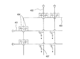
また、特許文献4には、図2に示すように、複数のゲート配線401および複数のドレイン配線402が交差するように形成され、各交差点に画素用の薄膜トランジスタ407が配置されたアリティブマトリクス基板において、基準電位の与えられる基準電位配線403と、ゲート配線401およびドレイン配線402との間にそれぞれESD保護用ダイオード404を設けることが開示されている。2つのダイオード404は、画素用の薄膜トランジスタ407の半導体層と同一の半導体膜を用いて形成されており、TFTのソースとゲートとをショートさせた構造を有している。このような構造のダイオードは「TFT型ダイオード」とも呼ばれる。2つのダイオード404のうち一方のゲート電極はゲート配線401に接続され、他方のゲート電極は基準電位配線403に接続されている。このため、ゲート配線401が、基準電位配線403に対して正負の何れに帯電しても、その電荷を打ち消す方向に、ゲート配線401と基準電位配線403との間に電流を流すことができる。従って、ESDによって発生するゲート配線およびドレイン配線間の電圧を抑制し、静電気によって薄膜トランジスタ407がダメージを受けることを防止できる。
Further, in
なお、図2は、画素用の薄膜トランジスタ407を保護するためのTFT型ダイオード404を図示しているが、例えば駆動回路などの回路で使用される回路用の薄膜トランジスタを保護するために、同様のTFT型ダイオードを用いることができる。
FIG. 2 shows a
図1および図2に示す例からわかるように、ESD保護回路は、保護しようとする配線に対し、プラス電荷がチャージされても、マイナス電荷がチャージされても、それらのチャージを逃がすことができるように、少なくとも2個のダイオードを有している。このため、回路規模が大きくなるという問題がある。 As can be seen from the examples shown in FIG. 1 and FIG. 2, the ESD protection circuit can release the charge even if a plus charge or a minus charge is charged to the wiring to be protected. Thus, it has at least two diodes. For this reason, there exists a problem that a circuit scale becomes large.
特に、ESD保護用ダイオードとして、移動度の比較的低いアモルファスシリコン膜などの半導体膜を用いたTFT型ダイオードを形成する場合、TFT型ダイオードのチャネル幅Wを大きくする必要があるので、ESD保護用ダイオードのサイズがさらに増大し、その結果、表示装置の額縁領域が拡大する。 In particular, when forming a TFT type diode using a semiconductor film such as an amorphous silicon film having a relatively low mobility as the ESD protection diode, it is necessary to increase the channel width W of the TFT type diode. The size of the diode is further increased, and as a result, the frame area of the display device is enlarged.
また、VDD配線を含まないシフトレジスタ回路に上記ESD保護回路を適用しようとすると、新たにVDD配線を外部から引き回す必要があり、それに伴い、回路規模がさらに増大する。 Further, if the ESD protection circuit is applied to a shift register circuit that does not include the VDD wiring, it is necessary to newly route the VDD wiring from the outside, and accordingly, the circuit scale further increases.
本発明は、上記の問題点に鑑みてなされたものであり、その目的は、複数の薄膜トランジスタと、ESDから薄膜トランジスタを保護するためのESD保護回路とを含む回路を備えた半導体装置において、ESDに起因する薄膜トランジスタのダメージを抑制しつつ、従来よりも回路規模を縮小することにある。 The present invention has been made in view of the above problems, and an object of the present invention is to provide a semiconductor device including a plurality of thin film transistors and an ESD protection circuit for protecting the thin film transistors from the ESD. The purpose is to reduce the circuit scale as compared with the prior art while suppressing the resulting damage to the thin film transistor.
本発明の半導体装置は、複数の薄膜トランジスタおよび少なくとも1つのダイオードを含む回路を備えた半導体装置であって、前記複数の薄膜トランジスタは同一の導電型を有し、前記複数の薄膜トランジスタの導電型がN型のとき、前記少なくとも1つのダイオードのカソード側の電極は、前記複数の薄膜トランジスタのうち何れか1つの薄膜トランジスタのゲートに接続された配線に接続されており、前記複数の薄膜トランジスタの導電型がP型のとき、前記少なくとも1つのダイオードのアノード側の電極は、前記複数の薄膜トランジスタのうち何れか1つの薄膜トランジスタのゲートに接続された配線に接続されており、前記配線には、前記少なくとも1つのダイオードと電流の流れる方向が逆になるように配置された他のダイオードが形成されていない。 The semiconductor device of the present invention is a semiconductor device including a circuit including a plurality of thin film transistors and at least one diode, wherein the plurality of thin film transistors have the same conductivity type, and the conductivity type of the plurality of thin film transistors is an N type. In this case, the cathode-side electrode of the at least one diode is connected to a wiring connected to the gate of any one of the plurality of thin film transistors, and the conductivity type of the plurality of thin film transistors is P-type. The electrode on the anode side of the at least one diode is connected to a wiring connected to a gate of any one of the plurality of thin film transistors, and the wiring includes the at least one diode and a current. Other diodes arranged so that the flow direction of There has not been formed.
ある好ましい実施形態において、前記回路の電圧波高値は20V以上である。 In a preferred embodiment, the voltage peak value of the circuit is 20V or more.
前記少なくとも1つの薄膜ダイオードおよび前記何れか1つの薄膜トランジスタの半導体層は、同一の半導体膜から形成されていることが好ましい。 The semiconductor layers of the at least one thin film diode and any one of the thin film transistors are preferably formed from the same semiconductor film.
前記同一の半導体膜は微結晶シリコン膜であってもよい。 The same semiconductor film may be a microcrystalline silicon film.
前記回路はシフトレジスタを含んでもよい。 The circuit may include a shift register.
ある好ましい実施形態において、前記シフトレジスタは、それぞれが出力信号を順次出力する複数の段を有し、前記複数の段のそれぞれは、前記出力信号を出力する第1トランジスタと、それぞれのソース領域またはドレイン領域が前記第1トランジスタのゲート電極に電気的に接続された複数の第2トランジスタとを有し、前記複数の第2トランジスタは、少なくとも2つのチャネル領域と、ソース領域と、ドレイン領域とを含む活性層を有するマルチチャネル型トランジスタを含む。 In a preferred embodiment, the shift register includes a plurality of stages each of which sequentially outputs an output signal, and each of the plurality of stages includes a first transistor that outputs the output signal and a respective source region or A drain region having a plurality of second transistors electrically connected to a gate electrode of the first transistor, the plurality of second transistors having at least two channel regions, a source region, and a drain region; A multi-channel transistor having an active layer.
前記少なくとも1つのダイオードは、基板上に形成されたゲート電極と、前記ゲート電極上に形成されたゲート絶縁層と、前記ゲート絶縁層上に形成され、第1領域と、第2領域とを有する少なくとも1つの半導体層と、前記第1領域上に設けられ、前記第1領域および前記ゲート電極と電気的に接続された第1電極と、前記第2領域上に設けられ、前記第2領域に電気的に接続された第2電極とを備えてもよい。 The at least one diode includes a gate electrode formed on the substrate, a gate insulating layer formed on the gate electrode, a first region, and a second region formed on the gate insulating layer. At least one semiconductor layer; a first electrode provided on the first region; and electrically connected to the first region and the gate electrode; provided on the second region; You may provide the 2nd electrode electrically connected.
前記少なくとも1つの半導体層は、前記ゲート絶縁層を介して前記ゲート電極と重なっているチャネル領域と、前記ゲート絶縁層を介して前記ゲート電極と重なっていない抵抗領域とを有し、前記ダイオードのオン状態において、前記第1電極と前記第2電極との間に、前記チャネル領域と前記抵抗領域とを含む電流経路が形成されていてもよい。 The at least one semiconductor layer has a channel region overlapping with the gate electrode via the gate insulating layer, and a resistance region not overlapping with the gate electrode via the gate insulating layer, In the on state, a current path including the channel region and the resistance region may be formed between the first electrode and the second electrode.
本発明によれば、単チャネルTFTからなる回路を備えた半導体装置において、回路規模の増大を抑えつつ、ESDに起因するTFTのオフリークの増大を抑制できる。従って、回路の誤動作を防止することができる。 According to the present invention, an increase in off-leakage of a TFT due to ESD can be suppressed while suppressing an increase in circuit scale in a semiconductor device including a circuit composed of a single channel TFT. Therefore, malfunction of the circuit can be prevented.
本発明を、駆動回路を備えたアクティブマトリクス基板に適用すると特に効果的である。 The present invention is particularly effective when applied to an active matrix substrate having a drive circuit.
本発明の半導体装置は、複数の薄膜トランジスタと、少なくとも1つのダイオードとを含む回路を備える。本発明における回路に含まれる薄膜トランジスタは、何れも同一の導電型を有する(何れもPチャネル型TFTであるか、またはNチャネル型TFTである)。本明細書では、このような回路を「単チャネルTFTからなる回路」と呼ぶ。 A semiconductor device of the present invention includes a circuit including a plurality of thin film transistors and at least one diode. The thin film transistors included in the circuit of the present invention all have the same conductivity type (all are P-channel TFTs or N-channel TFTs). In this specification, such a circuit is referred to as a “circuit composed of a single channel TFT”.
本発明では、同一の導電型を有する複数の薄膜トランジスタの導電型がN型のとき、少なくとも1つのダイオードのカソード側の電極は、複数の薄膜トランジスタのうち何れか1つの薄膜トランジスタのゲートに接続された配線に接続されている。複数の薄膜トランジスタの導電型がP型のときには、少なくとも1つのダイオードのアノード側の電極は、複数の薄膜トランジスタのうち何れか1つの薄膜トランジスタのゲートに接続された配線に接続されている。また、上記配線には、少なくとも1つのダイオードと電流の流れる方向が逆になるように配置された他のダイオードは形成されていない。 In the present invention, when the conductivity type of a plurality of thin film transistors having the same conductivity type is N type, the electrode on the cathode side of at least one diode is a wiring connected to the gate of any one of the plurality of thin film transistors It is connected to the. When the conductivity type of the plurality of thin film transistors is P-type, the anode-side electrode of at least one diode is connected to a wiring connected to the gate of any one of the plurality of thin film transistors. The wiring is not formed with at least one diode and other diodes arranged so that the direction of current flow is reversed.
本発明は、表示装置の駆動回路、アクティブマトリクス基板、またはそれを用いた表示装置などに広く適用できる。例えば薄型液晶テレビなどの比較的大型の表示装置では、アモルファスシリコン膜、微結晶シリコン膜、IGZO膜などのポリシリコンよりも移動度の低い半導体膜を用いて、画素用TFTのみでなく、駆動回路などの周辺回路に使用される回路用TFTが形成されることが好ましいが、このような回路用TFTは、一般に、単チャネルTFTである。すなわち、Nチャネル型TFTまたはPチャネル型TFTであり、CMOSを構成しない。 The present invention can be widely applied to a driving circuit of a display device, an active matrix substrate, or a display device using the same. For example, a relatively large display device such as a thin liquid crystal television uses a semiconductor film having a lower mobility than polysilicon such as an amorphous silicon film, a microcrystalline silicon film, and an IGZO film, and not only a pixel TFT but also a driving circuit. It is preferable to form circuit TFTs used for peripheral circuits such as the above, but such circuit TFTs are generally single-channel TFTs. That is, it is an N-channel TFT or a P-channel TFT and does not constitute a CMOS.
ここで、図面を参照しながら、本発明によって解決される課題を詳しく説明する。 Here, the problem solved by the present invention will be described in detail with reference to the drawings.
単チャネルTFTからなる回路では、LPSや単結晶ICで使用されているCMOSを含む回路に比べて、TFTのオフリーク電流が増大し、誤動作が発生しやすいという問題がある。この理由は次のとおりである。CMOSでは、ドーピング工程を利用してしきい値制御を行うことが可能である。これに対し、単チャネルTFTでは、通常、コスト削減のため、ドーピング工程を行わないので、しきい値を制御することができない。このため、Id−Vg特性のサブスレッショルド領域がVg=0[V]近傍にあり、オフ時にリークが生じる可能性が高いからである。 A circuit including a single channel TFT has a problem that an off-leak current of the TFT is increased and a malfunction is likely to occur as compared with a circuit including a CMOS used in an LPS or a single crystal IC. The reason for this is as follows. In CMOS, threshold control can be performed using a doping process. On the other hand, in a single channel TFT, since a doping process is not usually performed for cost reduction, the threshold value cannot be controlled. For this reason, the subthreshold region of the Id-Vg characteristic is in the vicinity of Vg = 0 [V], and there is a high possibility that leakage occurs at the time of off.
本発明者は、上記問題の原因を究明するために検討を重ねた結果、単チャネルTFTのゲートにプラスまたはマイナス電荷が入力されると、そのTFTの閾値が、印加された電荷の極性に応じて、プラスまたはマイナス方向にシフトすることがわかった。さらに、Nチャネル型の単チャネルTFTでは、閾値がマイナス方向にシフトする場合のみ、オフリーク電流が増大することを見出した。 As a result of repeated investigations to investigate the cause of the above problem, the present inventor, when a positive or negative charge is input to the gate of a single channel TFT, the threshold value of the TFT depends on the polarity of the applied charge. It turns out that it shifts in the positive or negative direction. Further, it has been found that in the N-channel type single channel TFT, the off-leakage current increases only when the threshold value shifts in the negative direction.
図3(a)および(b)は、それぞれ、Nチャネル型アモルファスシリコンTFTに対し、ゲートにプラス電荷(Vg=20V)をチャージするストレス試験、および、マイナス電荷(Vg=−20V)をチャージするストレス試験を行った結果を示すグラフである。ストレス試験におけるソース・ドレイン電圧は何れも0Vとする。グラフの縦軸は、Nチャネル型アモルファスシリコンTFTの閾値Vthの変化量(ΔVth)、横軸はストレス時間を表す。閾値の変化量ΔVthは、ストレスを所定時間印加した後の閾値からストレスを印加する前の閾値を引いた値である。 3A and 3B, respectively, a stress test in which a positive charge (Vg = 20V) is charged to the gate and a negative charge (Vg = −20V) is charged to the N-channel amorphous silicon TFT. It is a graph which shows the result of having performed the stress test. The source / drain voltage in the stress test is 0V. The vertical axis of the graph represents the amount of change (ΔVth) in the threshold value Vth of the N-channel amorphous silicon TFT, and the horizontal axis represents the stress time. The threshold change amount ΔVth is a value obtained by subtracting a threshold value before applying stress from a threshold value after applying stress for a predetermined time.
図3(a)に示す結果からわかるように、Nチャネル型アモルファスシリコンTFTでは、ゲートにプラス電荷を印加すると、閾値はプラス方向にシフトし、その結果、閾値が大きくなる。一方、図3(b)に示すように、ゲートにマイナス電荷を印加すると、閾値はマイナス方向にシフトし、その結果、閾値が小さくなる。 As can be seen from the results shown in FIG. 3A, in the N-channel amorphous silicon TFT, when a positive charge is applied to the gate, the threshold value shifts in the positive direction, and as a result, the threshold value increases. On the other hand, as shown in FIG. 3B, when a negative charge is applied to the gate, the threshold value shifts in the negative direction, and as a result, the threshold value decreases.
TFTの閾値がプラス方向にシフトしても、ゲートオフ時のリーク電流(オフリーク電流)は増えないが、マイナス方向にシフトすると、ゲートオフ時のリーク電流(オフリーク電流)が増大する。 Even if the threshold value of the TFT is shifted in the plus direction, the leakage current (off-leakage current) when the gate is off does not increase, but when it is shifted in the minus direction, the leakage current (off-leakage current) when the gate is off increases.
図4は、アモルファスシリコンTFTの電流(Id)−電圧(Vg)特性を示すグラフである。アモルファスシリコンTFTのチャネル長Lを4μm、チャネル幅Wを24μm、ドレイン電圧Vdを10V、ソース電圧VSSを−5Vとする。測定温度は室温とする。閾値がシフトする前では、曲線510で示すように、ゲートオフ時(Vg=VSS)には電流Id(off)はほとんど流れていない。しかしながら、閾値がマイナス方向にシフトすると、曲線512で示すように、ゲートオフ時の電流Id(off)は大幅に増大している。FIG. 4 is a graph showing current (Id) -voltage (Vg) characteristics of an amorphous silicon TFT. The channel length L of the amorphous silicon TFT is 4 μm, the channel width W is 24 μm, the drain voltage Vd is 10V, and the source voltage VSS is −5V. The measurement temperature is room temperature. Before the threshold value shifts, as indicated by a
ゲートオフ時の電流Id(off)が増大すると、このTFTを含む回路が誤動作する可能性がある。本実施形態における回路が例えばゲートドライバーである場合には、信号が出力されないおそれがある。逆に、閾値がプラス方向にシフトしたとしても、ゲートオフ時の電流Id(off)が増大しないので、オフリークに起因する回路の誤動作は生じにくいと考えられる。If the current Id (off) when the gate is off increases, the circuit including this TFT may malfunction. When the circuit in this embodiment is a gate driver, for example, there is a possibility that no signal is output. Conversely, even if the threshold value is shifted in the positive direction, the current Id (off) when the gate is turned off does not increase, so that it is considered that malfunction of the circuit due to off-leakage is unlikely to occur.
本発明者は、上記のような知見に基づいて、単チャネルTFTからなる回路では、TFTのゲートに印加されるプラスまたはマイナス電荷のうち、TFTのオフリーク電流を増大させる方の極性を有する電荷のみからTFTを保護すればよく、他方の極性を有する電荷から保護する必要がないことを見出し、本発明に至った。 Based on the above knowledge, the present inventor, in a circuit composed of a single channel TFT, only a charge having a polarity that increases the off-leakage current of the TFT among positive and negative charges applied to the gate of the TFT. Thus, the present inventors have found that it is only necessary to protect the TFT, and it is not necessary to protect from the charge having the other polarity.
すなわち、本発明では、単チャネルTFTとしてNチャネル型TFTを含む回路を備えた半導体装置において、Nチャネル型TFTのゲートにマイナス電荷がチャージされることを抑制するための保護用のダイオード(図1の保護回路ではダイオードD2)のみが形成されていればよい。一方、単チャネルTFTとしてPチャネル型TFTを含む回路を備えた半導体装置においては、Pチャネル型TFTのゲートにプラス電荷がチャージされることを抑制するための保護用のダイオード(図1の保護回路ではダイオードD1)のみが形成されていればよい。これにより、ESD保護用のダイオードの数を1/2に低減できるので、ESDによる回路の誤動作を防止しつつ、従来よりも回路規模を縮小することが可能になる。また、VDD配線を含まないシフトレジスタ回路に適用すると、ESD保護回路を形成する目的でVDD配線を引き回してくる必要がなくなり、回路規模をより効果的に縮小できる。 That is, according to the present invention, in a semiconductor device including a circuit including an N-channel TFT as a single-channel TFT, a protective diode (see FIG. 1) for suppressing negative charges from being charged to the gate of the N-channel TFT. In this protection circuit, only the diode D2) needs to be formed. On the other hand, in a semiconductor device including a circuit including a P-channel TFT as a single-channel TFT, a protective diode (a protection circuit in FIG. 1) for suppressing the positive charge from being charged to the gate of the P-channel TFT. Then, only the diode D1) needs to be formed. As a result, the number of diodes for ESD protection can be reduced to ½, so that it is possible to reduce the circuit scale as compared with the prior art while preventing malfunction of the circuit due to ESD. Further, when applied to a shift register circuit that does not include a VDD wiring, it is not necessary to route the VDD wiring for the purpose of forming an ESD protection circuit, and the circuit scale can be more effectively reduced.
(第1実施形態)
以下、図面を参照しながら、本発明による半導体装置の第1実施形態を説明する。(First embodiment)
A semiconductor device according to a first embodiment of the present invention will be described below with reference to the drawings.
本実施形態の半導体装置は、複数のTFTと、複数のTFTのうち少なくとも1つのTFTをESDから保護するための保護用ダイオードとを含む回路を備えている。複数のTFTは、何れもNチャネル型TFTであるか、あるいは、何れもPチャネル型TFTである(単チャネル構成)。保護用ダイオードは、保護しようとするTFTのゲートに接続された配線に設けられている。 The semiconductor device of this embodiment includes a circuit including a plurality of TFTs and a protective diode for protecting at least one TFT of the plurality of TFTs from ESD. The plurality of TFTs are all N-channel TFTs, or all are P-channel TFTs (single-channel configuration). The protection diode is provided on the wiring connected to the gate of the TFT to be protected.
図5(a)は、本実施形態における回路520の一部を例示する図である。回路520は、Nチャネル型の薄膜トランジスタ522と、薄膜トランジスタ522のゲートに接続された配線524と、VDD配線526と、保護用ダイオードD2を含む保護回路とを有している。保護用ダイオードD2は、例えばTFTのソースとゲートとをショートさせた構造を有し、「TFT型ダイオード」とも呼ばれる。
FIG. 5A is a diagram illustrating a part of the
図6は、保護用ダイオードD2を例示する模式的な断面図である。保護用ダイオードD2は、ゲート電極530と、ゲート電極530の上にゲート絶縁膜532を介して形成された半導体層534と、半導体層534の両端にそれぞれ電気的に接続された第1電極(ソース電極)536および第2電極(ドレイン電極)538とを有している。なお、電流はソースからドレインに流れるとする。半導体層534と、第1および第2電極536、538との間にはそれぞれコンタクト層540が形成されている。第1電極536はゲート電極530とコンタクトホール542内で接続されている。半導体層534のうち2つの電極536、538に挟まれた部分(チャネル部)544はゲート電極530と重なっている。保護用ダイオードD2では、第1電極536から半導体層534のチャネル部544を介して第2電極538に電流が流れる。本実施形態では、保護用ダイオードD2の第1電極(アノード側)536およびゲート電極530は、図5(a)に示すVSS配線526に接続され、第2電極(カソード側)538は配線524に接続されている。
FIG. 6 is a schematic cross-sectional view illustrating the protection diode D2. The protective diode D2 includes a
再び図5(a)を参照する。前述したように、薄膜トランジスタ522はNチャネル型であるため、薄膜トランジスタ522のゲートにマイナスの静電気が印加されると、閾値がマイナス方向にシフトし、オフリークが増大するおそれがある。この回路520では、配線524にマイナスの静電気が入力されると、保護用ダイオードD2によって静電気をVSS配線526に逃がすことができるので、薄膜トランジスタ522のゲートにマイナスの静電気が印加されることによるオフリークが増大することを抑制できる。
Reference is again made to FIG. As described above, since the
一方、配線524にプラスの静電気が入力されると、プラスのチャージを逃がすための保護回路は存在しないので、静電気はそのまま薄膜ダイオード522のゲートに印加される。しかしながら、この場合、薄膜トランジスタ522の閾値がプラス方向にシフトするため、この閾値シフトによってオフリークが増大することはない。
On the other hand, when positive static electricity is input to the
このように、本実施形態によると、ESDに起因する薄膜トランジスタ522のオフリークの増大を抑制することができる。また、従来は、1つの配線に対して、電流の流れる方向の異なる2つの保護用ダイオードが設けられていたが、本実施形態によると、1つの配線524に対して、1つの保護用ダイオードD2を設けることにより、薄膜トランジスタ522のオフリークの増大を抑制できるので、従来よりも回路規模を縮小できる。
Thus, according to this embodiment, an increase in off-leakage of the
図7は、本実施形態における保護用ダイオードD2の特性を例示するグラフである。グラフの横軸は、保護用ダイオードD2にかかる電圧Vdiode(V)、縦軸は保護用ダイオードD2を流れる電流(A)を示す。電圧VdiodeはVSS−Vg(Vg:配線24の電位)で表される。この例では、保護用ダイオードD2のチャネル幅Wを20μm、チャネル長Lを16μmとする。FIG. 7 is a graph illustrating characteristics of the protection diode D2 in the present embodiment. The horizontal axis of the graph represents the voltage V diode (V) applied to the protective diode D2, and the vertical axis represents the current (A) flowing through the protective diode D2. The voltage V diode is expressed by VSS-Vg (Vg: potential of the wiring 24). In this example, the protection diode D2 has a channel width W of 20 μm and a channel length L of 16 μm.
図7からわかるように、配線524にマイナス電荷が入力され、保護用ダイオードD2の正の電圧(VSS−Vg>0)がかかると(順バイアス)、保護用ダイオードD2の第1電極から第2電極に向かって電流が流れるので、配線524からVSS配線526にマイナス電荷を逃がすことができる。
As can be seen from FIG. 7, when a negative charge is input to the
一方、配線電位Vgが薄膜トランジスタ522の動作電圧範囲内(VSS≦Vg≦VDD)であれば、保護用ダイオードD2に負の電圧(VSS−Vg<0)がかかっても(逆バイアス)、保護用ダイオードD2には電流が流れない。 On the other hand, if the wiring potential Vg is within the operating voltage range of the thin film transistor 522 (VSS ≦ Vg ≦ VDD), even if a negative voltage (VSS−Vg <0) is applied to the protective diode D2 (reverse bias), No current flows through the diode D2.
なお、保護用ダイオードD2のチャネル幅Wおよびチャネル長Lは特に限定しないが、一般にチャネル幅Wが大きいと(例えば10μm以上)、ESDが入力された時に大量の電荷を放出できるので好ましい。より好ましくは、チャネル幅Wは20μm以上である。また、チャネル長Lが大きいと(例えば5μm以上)、負荷抵抗が大きくなり、正常動作時に保護用ダイオードD2を通じてリークが生じることを抑制できる。一方、チャネル幅Wおよびチャネル長Lが大きくなりすぎると回路規模の増大を引き起こすため、チャネル幅Wは1000μm以下、チャネル長Lは50μm以下であることが好ましい。 The channel width W and the channel length L of the protective diode D2 are not particularly limited. In general, a large channel width W (for example, 10 μm or more) is preferable because a large amount of charge can be discharged when ESD is input. More preferably, the channel width W is 20 μm or more. Further, when the channel length L is large (for example, 5 μm or more), the load resistance increases, and it is possible to suppress the occurrence of leakage through the protective diode D2 during normal operation. On the other hand, if the channel width W and the channel length L are too large, the circuit scale is increased. Therefore, the channel width W is preferably 1000 μm or less and the channel length L is preferably 50 μm or less.
本実施形態における回路520は、Nチャネル型薄膜トランジスタ522の代わりに、Pチャネル型薄膜トランジスタを有していてもよい。この場合、図5(b)に示すように、Pチャネル型薄膜トランジスタのゲートに接続される保護回路は、ドレインとゲートをショートさせた構造を有する保護用ダイオードD1を含む。保護用ダイオードD1のカソード側の電極(ドレイン)はVDD配線に接続され、アノード側の電極(ソース)は、Pチャネル型薄膜トランジスタ522’のゲートに接続された配線524’に接続されている。なお、この保護回路は、保護用ダイオードD1と電流の流れる方向が逆になるように配置された他のダイオードを含まない。これにより、配線524’にプラスの静電気が印加された場合に、静電気をVDD配線に逃がすことができるので、Pチャネル型薄膜トランジスタの閾値がプラス方向にシフトすることを防止できる。
The
回路520は、典型的には複数の同一導電型のTFTと、複数のTFTの少なくとも1つのTFTをESDから保護するためのESD保護回路とを備えている。ESD保護回路は、保護しようとするTFTのオフリークを増大させる極性を有するESDにのみ有効な保護用ダイオードD2を含み、かつ、その逆の極性を有するESDに有効な保護用ダイオードD1を含まない。なお、本実施形態の回路は、上記のような保護回路を少なくとも1つ備えていればよく、2以上のTFTのそれぞれに対して、上記のような保護回路が設けられていてもよい。また、2つの保護用ダイオードD1、D2を含む保護回路によって保護されたTFTを含んでいてもよい。
The
本実施形態は、電圧波高値が20V以上の回路を備えた半導体装置に適用されることが好ましい。このような半導体装置では、回路に含まれるTFTの閾値のシフト量が極めて大きいので、上記のような保護回路を設けることによって、特に顕著な効果を得ることができる。 The present embodiment is preferably applied to a semiconductor device including a circuit having a voltage peak value of 20 V or more. In such a semiconductor device, since the shift amount of the threshold value of the TFT included in the circuit is extremely large, a particularly remarkable effect can be obtained by providing the protection circuit as described above.
本実施形態における回路520は、例えば、液晶表示パネルに一体に(モノリシックに)形成されたシフトレジスタであってもよい。以下、本実施形態におけるシフトレジスタの構成を説明する。
The
図8(a)は、本発明による実施形態の液晶表示パネル600の模式的な平面図であり、図8(b)は、1つの画素の模式的な構造を示している。なお、図8(a)には、液晶表示パネル600のアクティブマトリクス基板601の構造を示し、液晶層や対向基板は省略している。液晶表示パネル600に、バックライトや電源等を設けることによって液晶表示装置が得られる。
FIG. 8A is a schematic plan view of a liquid
アクティブマトリクス基板601には、ゲートドライバー610と、ソースドライバー620とが一体に形成されている。液晶表示パネル600の表示領域には複数の画素が形成されており、画素に対応するアクティブマトリクス基板601の領域を参照符号632で示している。なお、ソースドライバー620はアクティブマトリクス基板601に一体に形成する必要は無い。別途作製されたソースドライバーIC等を公知の方法で実装しても良い。
A
図8(b)に示すように、アクティブマトリクス基板601は、液晶表示パネル600の1つの画素に対応する画素電極601Pを有している。画素電極601Pは画素用TFT601Tを介して、ソースバスライン601Sに接続されている。TFT601Tのゲート電極はゲートバスライン601Gに接続されている。
As shown in FIG. 8B, the
ゲートバスライン601Gには、ゲートドライバー610の出力が接続されており、線順次に走査される。ソースバスライン601Sには、ソースドライバー620の出力が接続されており、表示信号電圧(階調電圧)が供給される。
The
次に、図9は、ゲートドライバー610に含まれるシフトレジスタ610Bの構成を説明するブロック図である。シフトレジスタ610Bはアクティブマトリクス基板601を構成するガラス基板などの絶縁性の基板に支持されている。シフトレジスタ610Bを構成するTFTは、アクティブマトリクス基板601の表示領域に形成される画素用TFT601Tと同じプロセスで形成することが好ましい。
Next, FIG. 9 is a block diagram illustrating the configuration of the
図9には、シフトレジスタ610Bが有する複数の段(ステージ)の内のn−2からn+2の5段だけを模式的に示している。複数の段は、実質的に同一の構造を有し、カスケード接続されている。シフトレジスタ610Bの各段からの出力は、液晶表示パネル600の各ゲートバスライン601Gに与えられる。このようなシフトレジスタ610Bは、例えば、特開平8−87893号公報に記載されている。特開平8−87893号公報の開示内容を参考のために本明細書に援用する。
FIG. 9 schematically shows only five stages from n−2 to n + 2 among a plurality of stages (stages) included in the
図10はシフトレジスタ610Bの1つの段に用いられる構成を示す模式図であり、図11はシフトレジスタ610Bの各段の入出力信号の波形およびnetAの電圧波形を示している。また、図12はシフトレジスタ610Bのn−2からn+2の5段からの出力信号の波形を示している。図12に示すように、シフトレジスタ610Bは各段から順次出力信号Goutを出力する。
FIG. 10 is a schematic diagram showing a configuration used for one stage of the
図10に示すように、シフトレジスタ610Bの各段は、出力信号Goutを出力する第1トランジスタMGと、それぞれのソース領域またはドレイン領域が第1トランジスタMGのゲート電極に電気的に接続された複数の第2トランジスタ(MHd、MKd、MMdおよびMNd)とを有している。図10において、第1トランジスタMGは、いわゆるプルアップトランジスタであり、第1トランジスタMGのゲート電極に接続された配線をnetAという。本実施形態では、これらのトランジスタは何れもNチャネル型薄膜トランジスタである。また、第2トランジスタMKdのゲートに接続された配線550には、ESD保護用のダイオード(保護用ダイオード)D2aが設けられている。保護用ダイオードD2aの構成は、図6を参照しながら前述した構成と同様であってもよい。保護用ダイオードD2aのカソード側の電極は配線550に接続され、アノード側の電極は接地またはVSSに接続されている。
As shown in FIG. 10, each stage of the
各段からゲートバスライン601Gに対して出力信号Goutが出力されるのは画素書き込み時間のみである。1つの段に注目すると、1フレーム期間(全てのゲートバスライン601Gが順次選択され、再び当該ゲートバスラインが選択されるまでの期間)の中で大部分の時間に亘ってGoutの電位はVSSに固定されるように構成されている。
The output signal Gout is output from each stage to the
S信号(前段の出力信号Gout(n−1))によってnetAをプリチャージする。このとき、netAにソースまたはドレインが繋がるトランジスタMHd、MKdおよびMNdはオフである。 NetA is precharged by the S signal (previous output signal Gout (n−1)). At this time, the transistors MHd, MKd, and MNd whose source or drain is connected to netA are off.
次に、クロック信号CKがHighのとき、netAをプルアップする。このときに、出力信号Gout(n)がゲートバスライン601G(n本目)に出力され、このゲートバスライン601Gに接続されている画素用TFT601Tがオン状態となり、画素電極601Pにソースバスライン601Sから表示信号電圧が供給される。即ち、画素電極601Pと対向電極(不図示)と、これらの間の液晶層(不図示)によって構成される液晶容量が充電される。
Next, when the clock signal CK is High, netA is pulled up. At this time, the output signal Gout (n) is output to the
その後、リセット信号R(次段の出力信号Gout(n+1))によって、netAとGoutの電位をVSSにプルダウンする。 After that, the potentials of netA and Gout are pulled down to VSS by a reset signal R (next stage output signal Gout (n + 1)).
なお、出力信号Gout(n)を出力しない期間は、クロック信号CKおよびクロック信号CKBにより、トランジスタMKdでnetAを、トランジスタMLでGoutの電位をVSSに固定する。 Note that in a period during which the output signal Gout (n) is not output, the clock signal CK and the clock signal CKB fix the netA in the transistor MKd and the potential of Gout in the transistor ML to VSS.
ここで、容量CAP1は、netAの電位を保ち、出力を補助する。トランジスタMJは、リセット信号Rに応じて、出力信号Goutの電位をLowにする。トランジスタMLは、クロック信号CKBに応じて出力信号Goutの電位をLowにする。クリア信号CLRは1フレーム(垂直走査期間)に1度、垂直帰線期間(シフトレジスタの最終段が出力してから、最初の段が出力するまでの間)に、シフトレジスタの全ての段に供給され、全ての段のnetAをLowにする。なお、クリア信号CLRはシフトレジスタの最終段のリセット信号の役目も兼ねる。 Here, the capacitor CAP1 keeps the potential of netA and assists the output. In response to the reset signal R, the transistor MJ sets the potential of the output signal Gout to Low. The transistor ML sets the potential of the output signal Gout to Low in response to the clock signal CKB. The clear signal CLR is transmitted to all stages of the shift register once in one frame (vertical scanning period) and in the vertical blanking period (from the output of the last stage of the shift register to the output of the first stage). Supplied, netA of all stages is set to Low. The clear signal CLR also serves as a reset signal for the final stage of the shift register.
本実施形態では、保護用ダイオードD2aが設けられているので、以下のような利点を有する。 In the present embodiment, since the protective diode D2a is provided, it has the following advantages.
比較のため、図13に、保護用ダイオードD2aが設けられていない点以外は図10に示す回路と同様の構成を有する回路(比較例の回路)を示す。簡単のため、図10と同様の構成要素には同一の参照符号を付し、説明を省略する。図13に示す比較例の回路は、本出願人による未公開の特願2008−297297号に記載されている。特願2008−297297号の開示内容を参考のために本明細書に援用する。 For comparison, FIG. 13 shows a circuit (comparative circuit) having the same configuration as the circuit shown in FIG. 10 except that the protective diode D2a is not provided. For simplicity, the same components as those in FIG. 10 are denoted by the same reference numerals, and description thereof is omitted. The circuit of the comparative example shown in FIG. 13 is described in Japanese Patent Application No. 2008-297297 unpublished by the present applicant. The disclosure of Japanese Patent Application No. 2008-297297 is incorporated herein by reference.
比較例の回路では、netAをブートストラップする第2トランジスタ(Nチャネル型TFT)MKdは、外部からの信号CKに直接接続されているため、外部からESDの影響を受け易い。配線550から、第2トランジスタMKdにマイナスの静電気が印加されると、第2トランジスタMKdのオフリークが大きくなり、回路に誤作動を生じさせる可能性が高くなる。
In the circuit of the comparative example, the second transistor (N-channel TFT) MKd that bootstraps netA is directly connected to the signal CK from the outside, and thus is easily affected by ESD from the outside. When negative static electricity is applied from the
これに対し、本実施形態では、図10に示すように、配線550に保護用ダイオードD2aが設けられているので、配線550にマイナスの静電気が入力された場合でも、マイナスの静電気は保護用ダイオードD2aを介して回路の外部に逃がされ、第2トランジスタMKdに印加されない。従って、第2トランジスタMKdのオフリークの増大を抑制でき、ESDに起因する回路の誤動作を防止できる。
On the other hand, in the present embodiment, as shown in FIG. 10, since the protective diode D2a is provided in the
また、配線550には、保護用ダイオードD2aの電流の流れる方向と逆方向に電流を流すダイオードが設けられていない。配線550に、逆方向に電流を流すダイオードをさらに設けようとすると、そのようなダイオードを形成するだけでなく、そのダイオードを介して配線550から電荷(プラスチャージ)を逃がすための配線として、この回路には使用されていないVDD配線を引き回してくる必要がある。このため、回路規模が大幅に増大する。これに対し、本実施形態では、配線550に対して1個の保護用ダイオードD2aを形成すればよいので、回路規模の増大を抑えつつ、配線550および第2トランジスタMKdをESDから適切に保護できる。
Further, the
本実施形態における回路では、保護用ダイオードによって保護しようとするトランジスタは第2トランジスタMKdに限らない。第2トランジスタMKdの代わりに、あるいは、第2トランジスタMKdに加えて、他のトランジスタを保護する保護用ダイオードを設けることができる。 In the circuit in the present embodiment, the transistor to be protected by the protective diode is not limited to the second transistor MKd. Instead of the second transistor MKd or in addition to the second transistor MKd, a protective diode for protecting other transistors can be provided.
以下、図14〜図18を参照しながら、本実施形態における回路の他の例を説明する。 Hereinafter, another example of the circuit according to the present embodiment will be described with reference to FIGS.
図14に示す回路では、第2トランジスタMHdのゲートに接続された配線552に保護用ダイオードD2bが設けられている。保護用ダイオードD2bのカソード側の電極は配線552に接続され、アノード側の電極は接地またはVSSに接続されている。
In the circuit shown in FIG. 14, a protective diode D2b is provided in the
図13に示す比較例の回路では、netAから電位をプルダウンする第2トランジスタMHdは、外部からの信号Rに直接接続されているため、外部から入力されるESDの影響を受け易い。配線552から、第2トランジスタMHdにマイナスの静電気が印加されると、第2トランジスタMHdのオフリークが大きくなる。その結果、出力トランジスタMGにかかる電圧が降下し、回路に誤動作を生じさせる可能性がある。これに対し、図14に示す例では、配線552に保護用ダイオードD2bが設けられているので、配線552から第2トランジスタMHdにマイナスの静電気が印加されることを抑制できる。従って、ESDに起因する回路の誤動作を防止できる。
In the circuit of the comparative example shown in FIG. 13, since the second transistor MHd that pulls down the potential from netA is directly connected to the signal R from the outside, it is easily affected by ESD input from the outside. When negative static electricity is applied from the
図15に示す回路では、トランジスタMLのゲートに接続された配線554に保護用ダイオードD2cが設けられている。保護用ダイオードD2cのカソード側の電極は配線554に接続され、アノード側の電極は接地またはVSSに接続されている。
In the circuit shown in FIG. 15, a protective diode D2c is provided in the
比較例の回路(図13)では、トランジスタMLは、外部からの信号CKBに直接接続されているため、外部から入力されるESDの影響を受け易い。これに対し、図15に示す例では、配線554に保護用ダイオードD2cが設けられているので、配線554に入力されたマイナスの静電気がトランジスタMLに印加されることを抑制できる。従って、ESDによってトランジスタMLのオフリークが増大することを抑制できる。
In the circuit of the comparative example (FIG. 13), the transistor ML is directly connected to the signal CKB from the outside, and thus is easily affected by ESD input from the outside. On the other hand, in the example shown in FIG. 15, since the protective diode D2c is provided in the
図16に示す回路では、第2トランジスタMNdのゲートに接続された配線556に保護用ダイオードD2dが設けられている。保護用ダイオードD2dのカソード側の電極は配線556に接続され、アノード側の電極は接地またはVSSに接続されている。
In the circuit shown in FIG. 16, a protection diode D2d is provided on the
比較例の回路(図13)では、第2トランジスタMNdは、外部からの信号CLRに直接接続されているため、外部から入力されるESDの影響を受け易い。これに対し、図16に示す例では、配線554に保護用ダイオードD2bが設けられているので、配線554に入力されたマイナスの静電気が第2トランジスタMNdに印加されることを抑制できる。従って、ESDによってトランジスタMNdのオフリークが増大することを抑制できる。
In the circuit of the comparative example (FIG. 13), the second transistor MNd is directly connected to the signal CLR from the outside and thus is easily affected by ESD input from the outside. On the other hand, in the example shown in FIG. 16, since the protective diode D2b is provided in the
図17に示す回路では、出力トランジスタMGのゲートに接続された配線netAに保護用ダイオードD2eが設けられている。保護用ダイオードD2eのカソード側の電極はnetAに接続され、アノード側の電極は接地されている。 In the circuit shown in FIG. 17, a protection diode D2e is provided on the wiring netA connected to the gate of the output transistor MG. The cathode side electrode of the protective diode D2e is connected to netA, and the anode side electrode is grounded.
ESDによって出力トランジスタMGのオフリークが増大すると、出力Goutの波形がなまる、あるいは、出力トランジスタMGがオン状態にならないおそれがある。図17に示す例では、netAにおける出力トランジスタMGと第2トランジスタMHdとの間に保護用ダイオードD2eが設けられているので、出力トランジスタMGに静電気が印加されることを抑制でき、出力トランジスタMGのオフリーク増大による上記問題を防止できる。 When the off-leakage of the output transistor MG increases due to ESD, the waveform of the output Gout may be lost or the output transistor MG may not be turned on. In the example shown in FIG. 17, since the protective diode D2e is provided between the output transistor MG and the second transistor MHd in netA, it is possible to suppress static electricity from being applied to the output transistor MG. The above problem due to increased off-leakage can be prevented.
本実施形態における回路は、上述した保護用ダイオードD2a〜D2eのうち何れか1個を有していてもよいし、複数の保護用ダイオードを有していてもよい。保護用ダイオードD2a〜D2eのなかでは、保護用ダイオードD2a、D2b、D2c、D2dおよびD2eの順に、高いESD保護効果が得られる。図18に示すように、上述した保護用ダイオードD2a〜D2eを全て有していてもよい。これにより、ESDによる回路の誤動作をより効果的に防止できる。 The circuit in the present embodiment may have any one of the protection diodes D2a to D2e described above, or may have a plurality of protection diodes. Among the protective diodes D2a to D2e, a high ESD protection effect is obtained in the order of the protective diodes D2a, D2b, D2c, D2d, and D2e. As shown in FIG. 18, you may have all the protection diodes D2a-D2e mentioned above. Thereby, the malfunction of the circuit by ESD can be prevented more effectively.
なお、本実施形態における回路がPMOS単チャネル構成である場合には、上記配線550〜配線558のうち少なくとも1つの配線に、プラス電荷を逃がすことができるように保護用ダイオード(図1に示す保護用ダイオードD1)を設ければよい。
When the circuit in this embodiment has a PMOS single-channel configuration, a protective diode (protection shown in FIG. 1) is provided so that positive charge can be released to at least one of the
本実施形態における回路に含まれるトランジスタおよび保護用ダイオードは、同一の半導体膜を用いて形成されることが好ましい。半導体膜は、アモルファスシリコン膜、微結晶シリコン膜、金属酸化物半導体膜(例えばIGZO膜)などであってもよい。 The transistor and the protective diode included in the circuit in this embodiment are preferably formed using the same semiconductor film. The semiconductor film may be an amorphous silicon film, a microcrystalline silicon film, a metal oxide semiconductor film (for example, an IGZO film), or the like.
上記の例では、第2トランジスタMHd、MKd、MMdおよびMNdはマルチチャネル構造(ここではデュアルチャネル構造)を有するが、代わりに、シングルチャネル構造を有していてもよい。ただし、特に、これらのトランジスタを微結晶シリコン膜を用いて形成する場合には、これらのトランジスタはマルチチャネル構造(上記例では、デュアルチャネル構造)を有することが好ましい。この理由を以下に説明する。 In the above example, the second transistors MHd, MKd, MMd and MNd have a multi-channel structure (here, a dual-channel structure), but may alternatively have a single-channel structure. However, in particular, when these transistors are formed using a microcrystalline silicon film, these transistors preferably have a multi-channel structure (a dual channel structure in the above example). The reason for this will be described below.
netAをプルアップすると、netAにソースまたはドレインが繋がる第2トランジスタ(オフ状態にある)のソース・ドレイン間に大きな電圧(Vds)がかかる。このときプルアップされているnetAの電圧が、netAにソースまたはドレインが繋がる第2トランジスタのリーク電流により、本来のクロック信号CK(Low)により立ち下がる前に、低下する。netAの電圧が低下することによって、出力信号GoutがHighにならない、または出力信号Goutの波形がなまり、画素電極に十分な電圧を供給することができず、表示品位が低下する。 When netA is pulled up, a large voltage (Vds) is applied between the source and drain of the second transistor (in the off state) whose source or drain is connected to netA. At this time, the voltage of netA that has been pulled up is lowered before falling by the original clock signal CK (Low) due to the leakage current of the second transistor whose source or drain is connected to netA. When the voltage of netA decreases, the output signal Gout does not become high, or the waveform of the output signal Gout becomes distorted, so that a sufficient voltage cannot be supplied to the pixel electrode, and display quality is deteriorated.
シングルチャネル構造の微結晶シリコンTFTを用いてシフトレジスタを構成すると、これらのTFTのリーク電流は比較的大きいので、リーク電流に起因して、上記のような不良が発生する可能性が高くなる。これに対し、マルチチャネル構造の微結晶シリコンTFTのサブスレッショルド領域のリーク電流は、シングルチャネル構造を有する微結晶シリコンTFTよりも小さいので、netAおよび出力信号Goutの波形のなまりを抑制できる。 When a shift register is formed using microcrystalline silicon TFTs having a single channel structure, the leakage currents of these TFTs are relatively large, so that there is a high possibility that the above-described defects occur due to the leakage current. On the other hand, since the leakage current in the subthreshold region of the microcrystalline silicon TFT having the multi-channel structure is smaller than that of the microcrystalline silicon TFT having the single channel structure, it is possible to suppress rounding of the waveforms of the netA and the output signal Gout.
なお、複数の第2トランジスタの内の少なくとも1つのTFTにデュアルチャネル構造を導入すれば、そのトランジスタについてはリーク電流を低減できる。複数の第2トランジスタの一部のTFTにデュアルチャネル構造を導入する場合には、ソース・ドレイン間電圧Vdsが最も高いトランジスタMHd、MLおよびMMdにデュアルチャネル構造を導入することが好ましい。トランジスタMHdは、そのゲート電極が前段の出力(Gout(n−1))に接続され、ソース電極またはドレイン電極が出力トランジスタMGのゲート電極(netA)またはVSSに接続されている。トランジスタMNdは、そのゲート電極がクロック信号CKの配線に接続され、ソース電極またはドレイン電極が出力トランジスタMGのゲート電極(netA)またはVSSに接続されている。トランジスタMMdは、そのゲート電極とソース電極とが互いに接続(ダイオード接続)され、ゲート電極には前段の出力(S信号)が供給される。トランジスタMMdのドレイン電極はトランジスタMGのゲート電極(netA)に接続されている。もちろん、特性上は、複数の第2トランジスタの全てにマルチチャネル構造を導入することが好ましい。 Note that if a dual channel structure is introduced into at least one TFT of the plurality of second transistors, leakage current of the transistor can be reduced. When a dual channel structure is introduced into some TFTs of the plurality of second transistors, it is preferable to introduce a dual channel structure into the transistors MHd, ML and MMd having the highest source-drain voltage Vds. The transistor MHd has its gate electrode connected to the previous output (Gout (n−1)), and its source electrode or drain electrode connected to the gate electrode (netA) or VSS of the output transistor MG. The transistor MNd has a gate electrode connected to the wiring of the clock signal CK, and a source electrode or drain electrode connected to the gate electrode (netA) or VSS of the output transistor MG. The gate electrode and the source electrode of the transistor MMd are connected to each other (diode connection), and the previous output (S signal) is supplied to the gate electrode. The drain electrode of the transistor MMd is connected to the gate electrode (netA) of the transistor MG. Of course, in terms of characteristics, it is preferable to introduce a multichannel structure in all of the plurality of second transistors.
なお、「微結晶シリコン膜」は、微結晶粒からなる結晶相とアモルファス相との混合状態を有する膜を意味する。微結晶シリコン膜に占めるアモルファス相の体積率は例えば5%以上95%以下の範囲で制御され得る。なお、アモルファス相の体積率は好ましくは5%以上40%以下であり、この範囲では膜中欠陥の少ない良好な微結晶シリコン膜が得られるため、TFTのオンオフ比をより効果的に改善できる。また、微結晶シリコン膜に対して可視光を用いたラマン散乱スペクトル分析を行うと、そのスペクトルは、結晶シリコンのピークである520cm-1の波長で最も高いピークを有するとともに、アモルファスシリコンのピークである480cm-1の波長でブロードなピークを有する。480cm-1付近のアモルファスシリコンのピーク高さは、520cm-1付近にみられる結晶シリコンのピーク高さの例えば1/30以上1以下となる。Note that the “microcrystalline silicon film” means a film having a mixed state of a crystalline phase composed of microcrystalline grains and an amorphous phase. The volume ratio of the amorphous phase in the microcrystalline silicon film can be controlled in the range of 5% to 95%, for example. Note that the volume fraction of the amorphous phase is preferably 5% or more and 40% or less. In this range, a good microcrystalline silicon film with few defects in the film can be obtained, so that the on / off ratio of the TFT can be improved more effectively. When a Raman scattering spectrum analysis using visible light is performed on the microcrystalline silicon film, the spectrum has the highest peak at a wavelength of 520 cm −1 , which is the peak of crystalline silicon, and the peak of amorphous silicon. It has a broad peak at a wavelength of 480 cm −1 . 480cm peak height of the amorphous silicon around -1 becomes less than 1 or more for example 1/30 of the peak height of the crystalline silicon found in the vicinity of 520 cm -1.
比較のため、多結晶シリコン膜に対してラマン散乱スペクトル分析を行うと、アモルファス成分はほとんど確認されず、アモルファスシリコンのピークの高さはほぼゼロとなる。なお、多結晶シリコン膜を形成する際に、結晶化条件により、局所的にアモルファス相が残ってしまう場合があるが、そのような場合でも、多結晶シリコン膜に占めるアモルファス相の体積率は概ね5%未満であり、ラマン散乱スペクトル分析によるアモルファスシリコンのピーク高さは多結晶シリコンのピーク高さの概ね1/30未満となる。 For comparison, when the Raman scattering spectrum analysis is performed on the polycrystalline silicon film, almost no amorphous component is confirmed, and the peak height of the amorphous silicon becomes almost zero. When forming a polycrystalline silicon film, an amorphous phase may remain locally depending on crystallization conditions. Even in such a case, the volume ratio of the amorphous phase in the polycrystalline silicon film is approximately It is less than 5%, and the peak height of amorphous silicon by Raman scattering spectrum analysis is approximately less than 1/30 of the peak height of polycrystalline silicon.
このような微結晶シリコン膜は、CCP(容量結合プラズマ)方式や、例えばICP(誘導結合プラズマ)方式のような高密度プラズマCVDによって形成できる。プラズマCVDの装置方式や成膜条件によって、上述したピーク強度比を調整することが可能である。 Such a microcrystalline silicon film can be formed by a high-density plasma CVD method such as a CCP (capacitive coupling plasma) method or an ICP (inductively coupled plasma) method. The above-described peak intensity ratio can be adjusted by the plasma CVD apparatus method and film forming conditions.
上述してきたように、本実施形態では、静電気の極性と、静電気によるTFTの閾値のシフト方向とに着目し、TFTのオフリーク電流を増大させる極性を有する静電気に対してのみ有効な保護回路を設け、他方の極性を有する静電気に有効な保護回路を設けない。このため、保護回路数を低減でき、回路規模を縮小できる。 As described above, in this embodiment, focusing on the polarity of static electricity and the shift direction of the threshold value of the TFT due to static electricity, a protection circuit effective only against static electricity having a polarity that increases the off-leakage current of the TFT is provided. No protective circuit effective against static electricity having the other polarity is provided. For this reason, the number of protection circuits can be reduced, and the circuit scale can be reduced.
本実施形態におけるシフトレジスタの回路構成は、図10および図14〜図18に示す構成に限定されない。本実施形態は、例えば上述した特願2008−297297に例示されている他のシフトレジスタにも適用できる。他のシフトレジスタにおいても、特に外部の信号と直接接続された薄膜トランジスタに対して、本実施形態における保護用ダイオードを設けることにより、上記と同様の効果が得られる。 The circuit configuration of the shift register in the present embodiment is not limited to the configurations shown in FIGS. 10 and 14 to 18. The present embodiment can also be applied to other shift registers exemplified in Japanese Patent Application No. 2008-297297 described above. In other shift registers, the same effect as described above can be obtained by providing the protective diode in this embodiment particularly for a thin film transistor directly connected to an external signal.
なお、本実施形態における回路はシフトレジスタに限定されない。例えばDAC、TG、ラッチ、電源回路などに適用してもよく、上記と同様の効果が得られる。 Note that the circuit in this embodiment is not limited to a shift register. For example, the present invention may be applied to a DAC, TG, latch, power supply circuit, etc., and the same effect as described above can be obtained.
[保護用ダイオードの他の構成]
本実施形態における保護用ダイオードの構成は、図6を参照しながら前述した構成に限られない。例えば、アモルファスシリコンよりも移動度の高い半導体膜(例えば微結晶シリコン膜、金属酸化物半導体膜)を用いて保護用ダイオードの半導体層を形成する場合には、半導体層に電流が流れやすくなり、正常動作時においても保護用ダイオードに電流が流れてしまうおそれがある。このような問題を防止するために、半導体層内に、以下に説明するような抵抗領域を形成していてもよい。[Other configurations of protective diode]
The configuration of the protective diode in the present embodiment is not limited to the configuration described above with reference to FIG. For example, when a semiconductor layer of a protective diode is formed using a semiconductor film (for example, a microcrystalline silicon film or a metal oxide semiconductor film) having a higher mobility than amorphous silicon, current easily flows in the semiconductor layer. Even during normal operation, current may flow through the protective diode. In order to prevent such a problem, a resistance region as described below may be formed in the semiconductor layer.
図19は、本実施形態における他の保護用ダイオードを備えた半導体装置を例示する図であり、図19(a)は半導体装置の平面図、図19(b)は図1(a)のA−A’線およびB−B’線に沿った断面図である。 FIG. 19 is a diagram illustrating a semiconductor device provided with another protective diode according to this embodiment. FIG. 19A is a plan view of the semiconductor device, and FIG. 19B is A in FIG. It is sectional drawing along the -A 'line and the BB' line.
本実施形態の半導体装置は、基板1と、基板1上に形成されたダイオード201および薄膜トランジスタ301とを備えている。ダイオード201および薄膜トランジスタ301は、同一の半導体膜を用いて形成されている。薄膜トランジスタ301は例えばシフトレジスタの第2トランジスタであり、ダイオード201は第2トランジスタをESDから保護するための保護用ダイオードである。
The semiconductor device of this embodiment includes a
ここでは、半導体膜は、微結晶シリコン膜を用いて形成されている。薄膜トランジスタ301は、ボトムゲート構造を有する逆スタガーチャネルエッチング型TFTであり、ダイオード201は、ボトムゲート構造を有する逆スタガーチャネルエッチング型TFTを基本とし、そのゲート電極およびソース電極を接続した構造を有している。
Here, the semiconductor film is formed using a microcrystalline silicon film. The
薄膜トランジスタ301は、基板1の上に形成されたゲート電極103と、ゲート電極103を覆うように形成されたゲート絶縁層5と、ゲート絶縁層5上に形成された微結晶シリコン層107と、微結晶シリコン層107上にコンタクト層109aを介して形成されたソース電極110と、微結晶シリコン層107上にコンタクト層109bを介して形成されたドレイン電極112とを備える。
The
微結晶シリコン層107は、チャネル領域107cと、チャネル領域107cの両側にそれぞれ位置する第1領域107aおよび第2領域107bとを有している。第1領域107aは、コンタクト層109aによってソース電極110と電気的に接続されている。また、第2領域107bは、コンタクト層109bによってドレイン電極112と電気的に接続されている。チャネル領域107c上にはギャップ部116が形成されている。
The
ダイオード201は、基板1の上に形成されたゲート電極2、導電層3および接続配線4と、ゲート電極2、導電層3および接続配線4を覆うように形成されたゲート絶縁層5と、ゲート絶縁層5上にゲート電極2と重なるように配置された微結晶シリコン層6と、ゲート絶縁層5上に導電層3と重なるように配置された微結晶シリコン層7と、微結晶シリコン層6上にコンタクト層8aを介して形成された第1電極(ソース電極)10と、微結晶シリコン層6、7上にコンタクト層8b、9aを介して形成された中間電極11と、微結晶シリコン層7上にコンタクト層9bを介して形成された第2電極(ドレイン電極)12とを備える。
The
微結晶シリコン層6は、チャネル領域6cと、チャネル領域6cの両側にそれぞれ位置する第1領域6aおよび中間領域6bとを有している。第1領域6aは、コンタクト層8aによってソース電極10と電気的に接続されている。また、中間領域6bは、コンタクト層8bによって中間電極11と電気的に接続されている。同様に、微結晶シリコン層7は、抵抗体として機能する領域(以下、「抵抗領域」と称する。)7dと、抵抗領域7dの両側にそれぞれ位置する中間領域7aおよび第2領域7bとを有している。中間領域7aは、コンタクト層9aを介して中間電極11と電気的に接続されている。また、第2領域7bは、コンタクト層9bを介してドレイン電極12と電気的に接続されている。チャネル領域6c、抵抗領域7d上にはギャップ部15、16が形成されている。
The
本実施形態では、ゲート電極2、導電層3および接続配線4は、同一の導電膜から形成されている。ゲート電極2は、微結晶シリコン層6のチャネル領域6cと重なるように配置されており、チャネル領域6cの導電性を制御する。ゲート電極2は接続配線4と接続されており、接続配線4は、ゲート絶縁層5に設けられた開口部であるコンタクトホール14内で、ソース電極10と電気的に接続されている。また、図示しないが、ゲート電極2および接続配線4は、薄膜トランジスタ301のゲート電極103と電気的に接続されている。
In this embodiment, the
一方、導電層3は、微結晶シリコン層7と重なるように、すなわち抵抗領域7dの導電性を制御することが可能な位置に配置されている。ただし、導電層3は、ソース電極10等の他の電極、配線に接続されておらず、フローティングしている。
On the other hand, the
薄膜トランジスタ301およびダイオード201における微結晶シリコン層107、6、7は、複数の柱状の微結晶粒とアモルファス相からなる結晶粒界とを有している。微結晶シリコン層107、6、7に占めるアモルファス相の体積率は例えば5〜40%である。また、ラマン散乱スペクトル分析によるアモルファス相のピーク高さは、微結晶部分のピーク高さの1/3〜1/10倍である。なお、微結晶シリコン層107、6、7の代わりに、アモルファスシリコン層や多結晶シリコン層を活性層として用いてもよい。また、Zn−O系半導体(ZnO)膜、In−Ga−Zn−O系半導体(IGZO)膜、In−Zn−O系半導体(IZO)膜、Zn−Ti−O系半導体(ZTO)膜などの金属酸化物半導体からなる膜を活性層として用いてもよい。
The microcrystalline silicon layers 107, 6, and 7 in the
薄膜トランジスタ301およびダイオード201におけるコンタクト層109a、109b、8a、8b、9a、9bは、微結晶シリコン層107、6、7と対応する電極110、112、10、11、12との間の電気的導通を良好にするために設けられている。本実施形態では、これらのコンタクト層は、同一のn+型シリコン膜から形成されている。なお、これらのコンタクト層は、多結晶シリコン層、微結晶シリコン層またはアモルファスシリコン層などの単一の層であってもよいし、これらの層のうち少なくとも1つを含む積層構造を有していてもよい。なお、微結晶シリコン層の代わりに金属酸化物半導体からなる膜を活性層として用いる場合には、コンタクト層を用いなくてもよい。
また、薄膜トランジスタ301、ダイオード201における各電極110、112、10、11、12の上部には、ギャップ部116、15、16とその周辺を覆うようにパッシベーション13が設けられている。パッシベーション13は、窒化シリコン等の無機材料による膜、あるいはアクリル樹脂等の有機膜であってもよく、これらの積層物であってもよい。
Further, a
図示していないが、パッシベーション13には、フォトリソグラフィ等の手法によって、ソース電極110、10およびドレイン電極112、12に所定の電圧等の電気信号を入力するための開口部が適宜設けられ得る。ソース電極110、10およびドレイン電極112、12は、開口部や接続配線によって適切に接続され、外部から電気信号を入力できるような構成を有していてもよい。
Although not shown, the
ここで、薄膜トランジスタ301およびダイオード201の動作を説明する。
Here, operations of the
薄膜トランジスタ301では、ゲート電極103に印加する電圧により、チャネル領域107cの抵抗が十分に小さくなると、主にソース電極110とドレイン電極112との間に電流が流れる。このとき、電流は、ソース電極110からコンタクト層109aを経由して、微結晶シリコン層107の第1領域107a、チャネル領域107cおよび第2領域107bを流れる。この後、コンタクト層109bを経由してドレイン電極112に達する。
In the
ダイオード201では、ゲート電極2に印加される電圧により、チャネル領域6cの抵抗が十分に小さくなると、主にソース電極10とドレイン電極12との間に電流が流れる。このとき、電流は、ソース電極10からコンタクト層8aを経由して、微結晶シリコン層6の第1領域6a、チャネル領域6c、中間領域6bを流れる。この後、コンタクト層8bを経由して中間電極11に達する。中間電極11からも同様に、コンタクト層9aを経由して、微結晶シリコン層7の中間領域7a、抵抗領域7dおよび第2領域7bをこの順で流れ、その後、コンタクト層9bを経由してドレイン電極12に達する。
In the
前述したように、微結晶シリコン層7の下の導電層3は他の電極、配線に接続されないので、導電層3に直接電圧が印加されることはない。従って、微結晶シリコン層7の第1領域7a、抵抗領域7d、第2領域7bは常に高い抵抗値を有し、スイッチング素子ではなく抵抗体として機能する。ダイオード201では、このような抵抗体がソース電極10とドレイン電極12との間に位置しているので、これらの間の抵抗(オン抵抗)を大きくすることができる。従って、高移動度を有する微結晶シリコンを用いてダイオード201を形成した場合でも、ダイオード201に電流が流れすぎることを防止できる。このため、ダイオード201を、例えばショートリング用ダイオードなどの用途に好適に用いることができる。
As described above, since the
なお、図19では、ドレイン電極12側の微結晶シリコン層7がゲート電極2と重なっていないが、この微結晶シリコン層7がゲート電極2と重なっており、代わりにソース電極10側の微結晶シリコン層6がゲート電極2と重なっていなくても、上記と同様の効果が得られる。すなわち、ゲート電極2および導電層3の配置を入れ替えた構成でも、上記と同様の効果が得られる。
In FIG. 19, the
本実施形態および以下に述べる実施形態では、薄膜トランジスタおよびダイオードの半導体層(活性層)は、微結晶シリコン層などの単層であるが、例えば微結晶シリコン層とアモルファスシリコン層との積層構造を有していてもよい。同様に、ゲート電極、導電層、ソース電極、中間電極およびドレイン電極も単一の金属層などの導電物層から構成される必要はなく、同一または複数の導電物層からなる積層構造を有していてもよい。 In the present embodiment and the embodiments described below, the semiconductor layer (active layer) of the thin film transistor and the diode is a single layer such as a microcrystalline silicon layer, but has, for example, a stacked structure of a microcrystalline silicon layer and an amorphous silicon layer. You may do it. Similarly, the gate electrode, the conductive layer, the source electrode, the intermediate electrode, and the drain electrode do not need to be composed of a conductive layer such as a single metal layer, and have a laminated structure composed of the same or a plurality of conductive layers. It may be.
また、薄膜トランジスタおよびダイオードを支持する基板としては、ガラス基板の他に、プラスチック基板などの絶縁基板を用いることもできる。あるいは、表面に絶縁膜を有するステンレス基板を用いてもよい。また、上記基板は透明基板でなくてもよい。 In addition to a glass substrate, an insulating substrate such as a plastic substrate can be used as a substrate for supporting the thin film transistor and the diode. Alternatively, a stainless steel substrate having an insulating film on the surface may be used. The substrate may not be a transparent substrate.
さらに、本実施形態および以下に述べる実施形態の薄膜トランジスタおよびダイオードは、パッシベーション膜を有していなくてもよい。 Furthermore, the thin film transistors and diodes of this embodiment and the embodiments described below do not have to have a passivation film.
<半導体装置の製造方法>
次に、図面を参照しながら、図19に示す半導体装置の製造方法の一例を説明する。<Method for Manufacturing Semiconductor Device>
Next, an example of a method for manufacturing the semiconductor device shown in FIG. 19 will be described with reference to the drawings.
図20に示すように、半導体装置の製造方法は、ゲート電極を形成するゲート電極形成工程71、ゲート絶縁層および活性層となる島状の半導体層を形成するゲート絶縁層・半導体層形成工程72、ソースおよびドレイン電極を形成するソース・ドレイン電極形成工程73、ソースおよびドレイン電極を電気的に分離するソース・ドレイン分離工程74、および、パッシベーション形成工程75を含む。
As shown in FIG. 20, in the method of manufacturing a semiconductor device, a gate
以下、図21〜図24を参照しながら工程毎に詳しく説明する。図21〜図24は、半導体装置の製造方法の各工程を説明するための模式図である。図21(a)は平面図、図21(b)は図21(a)に示すA−A’線およびB−B’線に沿った断面図である。図22〜図24も同様であり、各図の(a)は平面図、各図の(b)は、対応する平面図のA−A’線およびB−B’線に沿った断面図である。 Hereinafter, each process will be described in detail with reference to FIGS. FIG. 21 to FIG. 24 are schematic views for explaining each step of the method for manufacturing the semiconductor device. FIG. 21A is a plan view, and FIG. 21B is a cross-sectional view taken along lines A-A ′ and B-B ′ shown in FIG. 22 to 24 are the same, (a) in each figure is a plan view, and (b) in each figure is a cross-sectional view along the AA ′ line and BB ′ line in the corresponding plan view. is there.
(1)ゲート電極形成工程71
図21(a)および(b)に示すように、基板1の上にゲート金属膜を形成し、これをパターニングすることにより、薄膜トランジスタ301のゲート電極103、ダイオード201のゲート電極2、導電層3および接続配線4を形成する。接続配線4およびゲート電極2は1つのパターン内になるよう隣接して形成される。また、導電層3は、ゲート電極2および接続配線4と分離したパターン内に形成される。(1) Gate
As shown in FIGS. 21A and 21B, a gate metal film is formed on the
具体的には、まず、アルゴン(Ar)ガスを用いたスパッタ法により、ガラス基板などの基板1の上にモリブデン(Mo)を0.2μmの厚さで堆積してゲート金属膜(図示せず)を形成する。ゲート金属膜を形成する際の基板1の温度は200〜300℃とする。
Specifically, first, molybdenum (Mo) is deposited to a thickness of 0.2 μm on a
続いて、ゲート金属膜の上にフォトレジスト材料によるレジストパターン膜(図示せず)を形成し、このレジストパターン膜をマスクとしてゲート金属膜のパターニングを行う(フォトリソグラフィ工程)。これにより、薄膜トランジスタ301のゲート電極103、ダイオード201のゲート電極2、導電層3および接続配線4を得る。ゲート金属膜のエッチングには例えばウェットエッチング法を用いる。エッチャントとしては、10〜80重量%の燐酸、1〜10重量%の硝酸、1〜10重量%の酢酸、及び残部水からなる溶液を用いることができる。エッチング終了後、レジストパターン膜を有機アルカリを含む剥離液を用いて除去する。
Subsequently, a resist pattern film (not shown) made of a photoresist material is formed on the gate metal film, and the gate metal film is patterned using the resist pattern film as a mask (photolithography process). Thereby, the
ゲート金属膜の材料は、モリブデン(Mo)の他に、インジウム錫酸化物(ITO)や、タングステン(W)、銅(Cu)、クロム(Cr)、タンタル(Ta)、アルミニウム(Al)、チタン(Ti)等の単体金属、またはそれらに窒素、酸素、あるいは他の金属を含有させた材料であってもよい。ゲート金属膜は、上記材料を用いた単一の層であってもよいし、積層構造を有していてもよい。例えば、ゲート電極2は、チタンおよびアルミニウムによるTi/Al/Ti積層膜であってよく、チタンおよび銅によるTi/Cu/Ti積層膜、あるいは銅およびモリブデンによるMo/Cu/Mo積層膜であってもよい。
In addition to molybdenum (Mo), the material of the gate metal film is indium tin oxide (ITO), tungsten (W), copper (Cu), chromium (Cr), tantalum (Ta), aluminum (Al), titanium It may be a simple metal such as (Ti) or a material containing nitrogen, oxygen, or another metal. The gate metal film may be a single layer using the above materials or may have a stacked structure. For example, the
ゲート金属膜の形成方法としては、スパッタ法の他、蒸着法等を用いることもできる。ゲート金属膜の厚さも特に限定されない。また、ゲート金属膜のエッチング方法も、上述したウェットエッチング法に限定されず、塩素(Cl2)ガス及び三塩化ホウ素(BCl3)ガス、CF4(四フッ化炭素)ガス、O2(酸素)等を組み合わせたドライエッチング法等を用いることもできる。As a method for forming the gate metal film, an evaporation method or the like can be used in addition to the sputtering method. The thickness of the gate metal film is not particularly limited. Further, the etching method of the gate metal film is not limited to the above-described wet etching method, and chlorine (Cl 2 ) gas, boron trichloride (BCl 3 ) gas, CF 4 (carbon tetrafluoride) gas, O 2 (oxygen) Etc.) can also be used.
(2)ゲート絶縁層・半導体層形成工程72
次いで、ゲート電極2および103、導電層3、および接続配線4の上に、ゲート絶縁層5、微結晶シリコン膜およびn+型シリコン膜をこの順に形成し、微結晶シリコン膜およびn+型シリコン膜をパターニングする。これにより、図22(a)および(b)に示すように、島状の微結晶シリコン加工膜118、17、18、n+型シリコン加工膜120、19、20を得る。この後、ゲート絶縁層5に、接続配線4の一部を露出するコンタクトホール14を設ける。(2) Gate insulating layer / semiconductor
Then, the
具体的には、まず、ゲート電極2等が形成された基板1に、プラズマ化学的気相成長(PECVD)法により、窒化シリコン(SiNx)からなるゲート絶縁層(厚さ:例えば0.4μm)5を形成する。本実施形態では、ゲート絶縁層5の形成を、平行平板型(容量結合型)の電極構造を有する成膜チャンバーを用いて、基板温度:250〜300℃、圧力:50〜300Pa、電力密度:10〜20mW/cm2の条件下で行う。また、成膜用のガスとして、シラン(SiH4)、アンモニア(NH3)、及び窒素(N2)の混合ガスを用いる。Specifically, first, a gate insulating layer (thickness: 0.4 μm, for example) made of silicon nitride (SiN x ) is formed on the
続いて、ゲート絶縁層5の形成で用いた成膜チャンバーと同一のチャンバーを用いて、微結晶シリコン膜(厚さ:例えば0.12μm)を形成する。本実施形態では、微結晶シリコン膜の形成は、基板温度:250〜300℃、圧力:50〜300Pa、電力密度:1〜30mW/cm2という条件で行い、成膜用のガスとして水素ガスで希釈したシランガスを用いる。シラン(SiH4)と水素(H2)との流量比は1:200〜1:1000とする。Subsequently, a microcrystalline silicon film (thickness: 0.12 μm, for example) is formed using the same chamber as that used for forming the
さらに、上記と同一の成膜チャンバーを用いて、n+型シリコン膜(厚さ:例えば0.05μm)を形成する。本実施形態では、n+型シリコン膜の形成は、微結晶シリコン膜の形成の場合とほぼ同様であるが、成膜用のガスとしてシラン(SiH4)と水素(H2)とホスフィン(PH3)との混合ガスを用いる。Further, an n + type silicon film (thickness: 0.05 μm, for example) is formed using the same film formation chamber as described above. In this embodiment, the formation of the n + -type silicon film is substantially the same as the formation of the microcrystalline silicon film, but silane (SiH 4 ), hydrogen (H 2 ), and phosphine (PH) are used as the deposition gases. 3 ) Use a mixed gas.
この後、ゲート絶縁層5の上にフォトレジスト材料によるレジストパターン膜(図示せず)を形成し、このレジストパターン膜をマスクとして微結晶シリコン膜およびn+型シリコン膜のパターニングを行う(フォトリソグラフィ工程)。これにより、島状の微結晶シリコン加工膜118、17、18、n+型シリコン加工膜120、19、20を得る。微結晶シリコン膜およびn+型シリコン膜のエッチングには例えば塩素(Cl2)ガスを主として用いたドライエッチング法を用いる。エッチング終了後、レジストパターン膜を有機アルカリを含む剥離液を用いて除去する。Thereafter, a resist pattern film (not shown) made of a photoresist material is formed on the
さらに、フォトレジスト材料によるレジストパターン膜(図示せず)を形成し、このレジストパターン膜をマスクとして、ゲート絶縁層5にコンタクトホール14を形成する(フォトリソグラフィ工程)。コンタクトホール14の形成には、例えばCF4(四フッ化炭素)ガス、O2(酸素)等を組み合わせたドライエッチング法等を用いることができる。エッチング終了後、レジストパターン膜を有機アルカリを含む剥離液を用いて除去する。Further, a resist pattern film (not shown) made of a photoresist material is formed, and a
(3)ソース・ドレイン電極形成工程73
n+型シリコン加工膜120、19、20およびゲート絶縁層5の上にソース・ドレイン電極形成用の導電膜を形成する。本実施形態では、アルゴン(Ar)ガスを用いたスパッタ法により、基板1の表面にモリブデンを0.2μmの厚さで堆積することにより、導電膜(厚さ:例えば0.2μm)を形成する。導電膜を形成する際の基板温度は200〜300℃とする。(3) Source / drain
A conductive film for forming source / drain electrodes is formed on the n + -type silicon processed
この後、図23(a)および(b)に示すように、導電膜上にレジストパターン膜21を形成し、これをマスクとして導電膜のパターニングを行うことにより、薄膜トランジスタ301のソース電極110、ドレイン電極112、および、ダイオード201のソース電極10、中間電極11、ドレイン電極12を得る。
Thereafter, as shown in FIGS. 23A and 23B, a resist
導電膜のパターニングは、例えばウェットエッチング法を用いて行うことができる。本実施形態では、エッチャントとして、10〜80重量%の燐酸、1〜10重量%の硝酸、1〜10重量%の酢酸、および残部水からなる溶液を用いる。ソース電極10、中間電極11およびドレイン電極12上のレジストパターン膜21は、エッチング終了後も除去することなく次工程まで残す。
The conductive film can be patterned using, for example, a wet etching method. In this embodiment, a solution comprising 10 to 80% by weight phosphoric acid, 1 to 10% by weight nitric acid, 1 to 10% by weight acetic acid, and the remaining water is used as the etchant. The resist
なお、導電膜の材料は、モリブデン(Mo)の他に、インジウム錫酸化物(ITO)や、タングステン(W)、銅(Cu)、クロム(Cr)、タンタル(Ta)、アルミニウム(Al)、チタン(Ti)等の単体金属、またはそれらに窒素、酸素、あるいは他の金属を含有させた材料であってもよい。ソース電極10等は、上記材料を用いた単一の層であってもよいし、積層構造を有していてもよい。例えば、導電膜は、チタンおよびアルミニウムによるTi/Al/Ti積層膜であってよく、チタンおよび銅によるTi/Cu/Ti積層膜、あるいは銅およびモリブデンによるMo/Cu/Mo積層膜であってもよい。 In addition to molybdenum (Mo), the conductive film is made of indium tin oxide (ITO), tungsten (W), copper (Cu), chromium (Cr), tantalum (Ta), aluminum (Al), It may be a simple metal such as titanium (Ti) or a material containing nitrogen, oxygen, or another metal. The source electrode 10 or the like may be a single layer using the above materials or may have a laminated structure. For example, the conductive film may be a Ti / Al / Ti laminated film made of titanium and aluminum, or a Ti / Cu / Ti laminated film made of titanium and copper, or a Mo / Cu / Mo laminated film made of copper and molybdenum. Good.
導電膜の形成方法としては、スパッタ法の他、蒸着法等を用いることもできる。また、導電膜の形成方法も上述したエッチャントを用いたウェットエッチングに限定されない。さらに、導電膜の厚さも上記の厚さに限定されない。 As a method for forming the conductive film, an evaporation method or the like can be used in addition to the sputtering method. Further, the method for forming the conductive film is not limited to the wet etching using the above-described etchant. Furthermore, the thickness of the conductive film is not limited to the above thickness.
(4)ソース・ドレイン分離工程74
続いて、図24(a)および(b)に示すように、n+型シリコン加工膜120のうちソース電極110およびドレイン電極112の何れにも覆われていない部分を除去し、ギャップ部116を形成する。同様に、n+型シリコン加工膜19、20のうち、ソース電極10、中間電極11およびドレイン電極12の何れにも覆われていない部分を除去し、それぞれギャップ部15、16を形成する。このとき、微結晶シリコン加工膜118、17、18のうちギャップ部116、15、16に位置する部分は、オーバーエッチングによって他の部分よりも薄くなる。これにより、微結晶シリコン加工膜118およびn+型シリコン加工膜120から、微結晶シリコン層107およびコンタクト層109a、109bを得る。同様に、微結晶シリコン加工膜17、18およびn+型シリコン加工膜19、20から、それぞれ、微結晶シリコン層6、7およびコンタクト層8a、8b、9a、9bを得る。エッチング後、レジストパターン膜21を除去する。(4) Source /
Subsequently, as shown in FIGS. 24A and 24B, a portion of the n + -type silicon processed
本実施形態では、n+型シリコン加工膜120、19、20のエッチングには、塩素(Cl2)ガスを用いたドライエッチング法を用いる。レジストパターン膜21は、エッチング終了後に有機アルカリを含む剥離液を用いて除去する。なお、エッチング方法は上記の方法に限定されない。In this embodiment, a dry etching method using chlorine (Cl 2 ) gas is used for etching the n + -type silicon processed
(5)パッシベーション形成工程75
次いで、薄膜トランジスタ301のソース電極110、ドレイン電極112、ギャップ部116およびそれらの周囲と、ダイオード201のソース電極10、中間電極11、ドレイン電極12、ギャップ部15、16およびそれらの周囲とを覆うように窒化シリコン(SiNx)からなるパッシベーション13を形成する。このようにして、図19(a)および(b)に示す半導体装置が得られる。(5)
Next, the
具体的には、プラズマ化学的気相成長(PECVD)法により、窒化シリコン(SiNx)からなるパッシベーション13(厚さ:例えば0.3μm)を形成する。本実施形態では、パッシベーション13の形成を、平行平板型(容量結合型)の電極構造を有する成膜チャンバーを用いて、基板温度:200℃、圧力:50〜300Pa、電力密度:10〜20mW/cm2の条件下で行う。また、成膜用のガスとして、シラン(SiH4)、アンモニア(NH3)、及び窒素(N2)の混合ガスを用いる。Specifically, a passivation 13 (thickness: 0.3 μm, for example) made of silicon nitride (SiN x ) is formed by plasma chemical vapor deposition (PECVD). In this embodiment, the
パッシベーション13には、図示していないが、ソース電極110、10およびドレイン電極112、12等に所定の電圧等の電気信号を入力するための開口部が適宜設けられ得る。
Although not shown, the
本実施形態におけるダイオードでは、オン状態において、半導体層のチャネル領域および抵抗領域を含む電流経路が形成されれば、図19に示すダイオードと同様の効果を得ることができる。例えばダイオードは、3つ以上の島状の微結晶シリコン層を有していてもよい。この場合でも、少なくとも1つの微結晶シリコン層がゲート電極と重なっておらず、他の微結晶シリコン層がゲート電極と重なるチャネル領域を有していれば、上記と同様の効果が得られる。また、図19に示す例では、半導体層(微結晶シリコン層6、7)およびコンタクト層8a、8b、9a、9bは島状であるが、必ずしも島状である必要はない。さらに、ダイオード201は、導電層3を有していなくてもよい。
In the diode of this embodiment, the same effect as that of the diode shown in FIG. 19 can be obtained if a current path including the channel region and the resistance region of the semiconductor layer is formed in the on state. For example, the diode may include three or more island-shaped microcrystalline silicon layers. Even in this case, the effect similar to the above can be obtained as long as at least one microcrystalline silicon layer does not overlap with the gate electrode and another microcrystalline silicon layer has a channel region overlapping with the gate electrode. In the example shown in FIG. 19, the semiconductor layers (
また、薄膜トランジスタの構成も、図19に示す構成に限定されない。図19に示す薄膜トランジスタ301は何れも1つのゲート電極103を有するが、複数のゲート電極を有していてもよい。その場合、各ゲート電極上にそれぞれ島状の微結晶シリコン層が配置されていてもよいし、複数のゲート電極と重なるように1つの微結晶シリコン層が配置されていてもよい。あるいは、後で詳しく説明するように、1つのゲート電極上に配置された微結晶シリコン層に複数のチャネル領域が形成されていてもよい。
Further, the structure of the thin film transistor is not limited to the structure shown in FIG. Although each of the
このように、半導体層の電流経路となる部分の一部がゲート電極と重ならないように構成すると、第1電極に正の電位を与えた場合でも、半導体層のうちゲート電極と重なっていない部分には、ゲート電極を通じて正の電位を与えられないので、可動電荷である電子の蓄積がなされず、この部分の電気抵抗が下がらない。このため、ゲート電極と重なっていない部分は、チャネル領域と直列に接続された電気抵抗となる。 As described above, when a part of a portion of the semiconductor layer that becomes a current path does not overlap with the gate electrode, a portion of the semiconductor layer that does not overlap with the gate electrode even when a positive potential is applied to the first electrode. Since a positive potential cannot be applied through the gate electrode, electrons that are mobile charges are not accumulated, and the electrical resistance of this portion does not decrease. For this reason, the portion not overlapping with the gate electrode becomes an electric resistance connected in series with the channel region.
従って、半導体層のうちゲート電極と重なっていない部分のサイズ(面積)を調整することにより、ダイオードに適切な大きさの直列の電気抵抗を与えることができる。アモルファスシリコンを用いた従来の保護用ダイオードと同等の特性を実現することも可能である。 Therefore, by adjusting the size (area) of the portion of the semiconductor layer that does not overlap with the gate electrode, an appropriate series electric resistance can be given to the diode. It is also possible to realize characteristics equivalent to those of a conventional protective diode using amorphous silicon.
ダイオードの半導体層のうちゲート電極と重なっていない部分は、ダイオードの第1電極と接続されていない導電層の上に配置されていてもよい。ここでいう「導電層」は、例えばゲート電極と同一の導電膜から形成され、開放状態(フローティング状態)にある層であってもよい。特に本発明を表示装置に適用する場合、半導体層のうちゲート電極と重なっていない部分の下方に導電層が設けられていると、導電層によって、バックライトからの光による半導体層の特性変化(光劣化)を抑制できるので好ましい。 A portion of the semiconductor layer of the diode that does not overlap with the gate electrode may be disposed on a conductive layer that is not connected to the first electrode of the diode. Here, the “conductive layer” may be a layer formed of the same conductive film as the gate electrode, for example, and in an open state (floating state). In particular, when the present invention is applied to a display device, if a conductive layer is provided below a portion of the semiconductor layer that does not overlap with the gate electrode, the conductive layer changes the characteristics of the semiconductor layer due to light from the backlight ( Photodegradation) can be suppressed, which is preferable.
なお、薄膜トランジスタ301、302、ダイオード201、202、204は、微結晶シリコン層の代わりに、アモルファスシリコン層や多結晶シリコン層を活性層として用いてもよい。また、Zn−O系半導体(ZnO)膜、In−Ga−Zn−O系半導体(IGZO)膜、In−Zn−O系半導体(IZO)膜、Zn−Ti−O系半導体(ZTO)膜などの金属酸化物半導体からなる膜を活性層として用いてもよい。この場合、コンタクト層25a、25b、25d、25e、109a、109bは不要であって、活性層とソース・ドレイン電極は直接電気的接続をとることができる。特にIGZOのような金属酸化物半導体を用いた場合には、移動度が4cm2/Vsを超えるので、本発明を適用することによってさらに高い効果が得られる。Note that the
ただし、多結晶シリコン膜およびアモルファスシリコン膜を用いる場合には、抵抗領域を形成するメリットは小さい。多結晶シリコン膜を用いると、ダイオードの半導体層の一部にドーピングする不純物濃度を調整すれば、ダイオードの抵抗を大きくするなどの調節が容易だからである。また、アモルファスシリコン膜を用いると、ダイオードの抵抗が十分に高く、ダイオードの電流を大幅に低下させる必要がない場合が多いからである。 However, when a polycrystalline silicon film and an amorphous silicon film are used, the merit of forming the resistance region is small. This is because, when a polycrystalline silicon film is used, adjustment such as increasing the resistance of the diode is easy if the impurity concentration doped in a part of the semiconductor layer of the diode is adjusted. In addition, when an amorphous silicon film is used, the resistance of the diode is sufficiently high, and it is often unnecessary to significantly reduce the current of the diode.
図25は、本実施形態における他のダイオードを模式的に示す図であり、図25(a)は他のダイオードの平面図、図25(b)は図25(a)のE−E’線に沿った断面図である。図25に示すダイオードは、1つの島状半導体層を用いて形成されている点で、図19に示すダイオード201と異なっている。簡単のため、図19に示すダイオード201と同様の構成要素には同一の参照符号を付し、説明を省略する。
FIG. 25 is a diagram schematically showing another diode in the present embodiment, FIG. 25 (a) is a plan view of the other diode, and FIG. 25 (b) is a line EE ′ in FIG. 25 (a). FIG. The diode shown in FIG. 25 is different from the
ダイオード205は、ボトムゲート構造を有する逆スタガーチャネルエッチング型TFTを基本とし、そのゲート電極およびソース電極を接続した構造を有している。図示しないが、ダイオード205と同一基板上にTFTをさらに備える。このTFTは、ダイオード205の微結晶シリコン層27と同一の微結晶シリコン膜を用いて形成された活性層を有していればよく、例えば、図19(a)および(b)に示す薄膜トランジスタ301と同様の構成を有していてもよい。
The
ダイオード205は、ガラス基板などの基板1と、基板1の上に形成されたゲート電極26と、基板1の上にゲート電極26を覆うように形成されたゲート絶縁層5と、ゲート絶縁層5の上に形成された微結晶シリコン層27と、微結晶シリコン層27上にコンタクト層8aを介して形成されたソース電極10と、微結晶シリコン層27上にコンタクト層8bを介して形成されたドレイン電極12とを備える。
The
微結晶シリコン層27は、チャネル領域27cと、チャネル領域27cの両側にそれぞれ位置する第1および第2領域27a、27bとを有している。第1領域27aは、コンタクト層8aによってソース電極10と電気的に接続されている。また、第2領域27bは、コンタクト層8bによってドレイン電極12と電気的に接続されている。
The
チャネル領域27cは、ゲート電極26と重なるように配置されており、ゲート電極26に印加する電圧によってチャネル領域27cの導電性が制御され得る。また、微結晶シリコン層27は、第1および第2領域27a、27bとの間に位置し、ゲート電極26と重なっていない部分(抵抗領域)27dを有している。抵抗領域27dは、ゲート電極26に電圧を印加しても低抵抗化されないので、抵抗体として機能する。チャネル領域27cおよび抵抗領域27dのチャネル方向の長さL、LRは適宜調整されるが、例えばチャネル幅Wが10μmのとき、チャネル領域27cの長さ(チャネル長)Lは3μm、抵抗領域27dの長さLRは3μmである。なお、図25に示す例では、第2領域27bもゲート電極26と重なっていないので、第2領域27bも抵抗体として機能する。The
図25に示す例では、コンタクト層8a、8b、ソース電極10およびドレイン電極12は、チャネル領域27cおよび抵抗領域27dの上に位置しないようにパターニングされており、これによって、チャネル領域27cおよび抵抗領域27dの上にギャップ部15が形成されている。ゲート電極26、接続配線4およびTFTのゲート電極(図示せず)は、同一の導電膜から形成されている。ゲート電極26は接続配線4と接続されており、接続配線4は、ゲート絶縁層5に設けられた開口部であるコンタクトホール14内で、ソース電極10と電気的に接続されている。
In the example shown in FIG. 25, the contact layers 8a and 8b, the
なお、ダイオード205における微結晶シリコン層27、コンタクト層8a、8b、パッシベーション13の材料は、図19に示すダイオード201における対応する構成要素の材料と同様であってもよい。
Note that the material of the
ダイオード205では、主にソース電極10とドレイン電極12との間に電流が流れる。このとき、電流はソース電極10からコンタクト層8aを経由して、微結晶シリコン層27の第1領域27a、チャネル領域27cおよび抵抗領域27d、第2領域27bを流れる。この後、コンタクト層8bを経由してドレイン電極12に達する。
In the
図25に示す例でも、微結晶シリコン層27のうち抵抗領域27dおよび第2領域27bの下方にはゲート電極26が配置されないので、ゲート電極26へ電圧を印加した場合でも可動電荷である電子の蓄積がなされない。従って、抵抗領域27dおよび第2領域27bは、ゲート電極26の電位の影響をほとんど受けずに常に高抵抗である。このような抵抗の高い領域27dを微結晶シリコン層15に設けて、ソース電極10とドレイン電極12との間に電流を流れにくくすることにより、ダイオード205の用途に応じた特性を実現できる。
Also in the example shown in FIG. 25, since the
なお、上記ダイオードは、チャネル領域27cおよび抵抗領域27dの両方を有する半導体層を少なくとも1つ備えていればよく、そのような半導体層を含む2以上の半導体層を備えていてもよい。この場合、2以上の半導体層は、半導体層上に設けられた中間電極によって互いに接続されていてもよい。
Note that the diode only needs to include at least one semiconductor layer having both the
図25に示す半導体装置は、図20〜図24を参照しながら前述した方法と同様の方法で作製できる。 The semiconductor device shown in FIG. 25 can be manufactured by a method similar to the method described above with reference to FIGS.
図26は、本実施形態におけるさらに他のダイオードを示す図であり、図26(a)は平面図、図26(b)は図26(a)のF−F’線に沿った断面図である。図26に示すダイオードでは、ダイオードの半導体層の下方に2つのゲート電極が設けられ、かつ、ダイオードのソース・ドレイン電極間に中間電極が設けられていない点で、図19に示すダイオード201と異なっている。簡単のため、図19に示すダイオード201と同様の構成要素には同一の参照符号を付し、説明を省略する。
26A and 26B are diagrams showing still another diode according to the present embodiment, in which FIG. 26A is a plan view, and FIG. 26B is a cross-sectional view taken along line FF ′ in FIG. is there. The diode shown in FIG. 26 is different from the
ダイオード206は、ボトムゲート構造を有する逆スタガーチャネルエッチング型TFTを基本とし、そのゲート電極およびソース電極を接続した構造を有している。図示しないが、ダイオード206と同一基板上には、ボトムゲート構造を有する逆スタガーチャネルエッチング型TFTが設けられている。このTFTは、ダイオード206の微結晶シリコン層と同一の微結晶シリコン膜を用いて形成された活性層を有していればよく、例えば、図19(a)および(b)に示す薄膜トランジスタ301と同様の構成を有していてもよい。
The
ダイオード206は、ガラス基板などの基板1と、基板1の上に間隔を空けて配置されたゲート電極2、29と、基板1の上にゲート電極2、29を覆うように形成されたゲート絶縁層5と、ゲート絶縁層5の上に形成された微結晶シリコン層30と、微結晶シリコン層30上にコンタクト層8aを介して形成されたソース電極10と、微結晶シリコン層30上にコンタクト層9bを介して形成されたドレイン電極12とを備える。ゲート電極2およびゲート電極29は、接続電極4およびコンタクトホール14内でソース電極10と電気的に接続されている。
The
微結晶シリコン層30は、チャネル領域30c、30eと、チャネル領域30c、30eの間に位置する抵抗領域30dと、チャネル領域30c、30eの両側にそれぞれ位置する第1および第2領域30a、30bとを有している。第1領域30aは、コンタクト層8aによってソース電極10と電気的に接続されている。また、第2領域30bは、コンタクト層9bによってドレイン電極12と電気的に接続されている。
The
チャネル領域30cはゲート電極2と重なるように配置されており、ゲート電極2に印加する電圧によってチャネル領域30cの導電性が制御され得る。同様に、チャネル領域30eはゲート電極29と重なるように配置されており、ゲート電極29に印加する電圧によってチャネル領域30eの導電性が制御され得る。一方、抵抗領域30dは、ゲート電極2、29と重なっておらず、これらのゲート電極2、29に電圧を印加しても低抵抗化されないので、抵抗体として機能する。
The
チャネル領域30c、30eおよび抵抗領域30dのチャネル方向の長さL1、L2、LRは適宜調整されるが、例えばチャネル幅Wが10μmのとき、チャネル領域30c、30eの合計長さ(チャネル長L:L=L1+L2)は6μm、抵抗領域30dの長さLRは3μmである。The lengths L 1 , L 2 and L R in the channel direction of the
なお、ダイオード206における微結晶シリコン層30、コンタクト層8a、9b、パッシベーション13の材料は、図19に示すダイオード201における対応する構成要素の材料と同様であってもよい。
Note that the material of the
ダイオード206では、主にソース電極10とドレイン電極12との間に電流が流れる。このとき、電流はソース電極10からコンタクト層8aを経由して、微結晶シリコン層30の第1領域30a、チャネル領域30c、抵抗領域30d、チャネル領域30e、および第2領域30bをこの順で流れる。この後、コンタクト層9bを経由してドレイン電極12に達する。
In the
ダイオード206でも、微結晶シリコン層30のうち抵抗領域30dの下方にはゲート電極2、29が配置されないので、抵抗領域30dは、ゲート電極2、29の電位の影響をほとんど受けずに常に高抵抗である。このような抵抗の高い領域30dを微結晶シリコン層30に設けて、ソース電極10とドレイン電極12との間に電流を流れにくくすることにより、ダイオード206の用途に応じた特性を実現できる。
Even in the
図26に示す半導体装置も、図20〜図24を参照しながら前述した方法と同様の方法で作製できる。 The semiconductor device shown in FIG. 26 can also be manufactured by a method similar to the method described above with reference to FIGS.
図27は、本実施形態におけるさらに他の半導体装置を示す断面図である。図27に示す例では、In−Ga−Zn−O系半導体(IGZO)膜を用いてダイオードおよび薄膜トランジスタの活性層を形成している点、およびコンタクト層を有しない点で、図19に示す構成と異なっている。 FIG. 27 is a cross-sectional view showing still another semiconductor device according to the present embodiment. In the example illustrated in FIG. 27, the active layer of the diode and the thin film transistor is formed using an In—Ga—Zn—O-based semiconductor (IGZO) film, and the configuration illustrated in FIG. 19 is not provided. Is different.
半導体装置は、基板31と、基板31上に形成されたダイオード207および薄膜トランジスタ307とを備えている。ダイオード207および薄膜トランジスタ307は、同一のIGZO膜を用いて形成されている。薄膜トランジスタ207は、ボトムゲート構造を有する逆スタガーチャネルエッチング型TFTであり、ダイオード307は、ボトムゲート構造を有する逆スタガーチャネルエッチング型TFTを基本とし、そのゲート電極およびソース電極を接続した構造を有している。
The semiconductor device includes a
薄膜トランジスタ307は、基板31の上に形成されたゲート電極32と、ゲート電極32を覆うように形成されたゲート絶縁層35と、ゲート絶縁層35上に形成されたIGZO層50と、IGZO層50上に形成されたソース電極54およびドレイン電極52とを備える。
The
IGZO層50は、チャネル領域50cと、チャネル領域50cの両側にそれぞれ位置するソース領域50aおよびドレイン領域50bとを有している。ソース領域50aは、ソース電極54と接している。また、ドレイン領域50bはドレイン電極52と接している。
The
ダイオード207は、基板31の上に形成されたゲート電極33および接続配線34と、ゲート電極33および接続配線34を覆うように形成されたゲート絶縁層35と、ゲート絶縁層35上にゲート電極33と重なるように配置されたIGZO層40と、IGZO層40上に形成された第1電極(ソース電極)44と、IGZO層40上に形成された第2電極(ドレイン電極)42とを備える。
The
IGZO層40は、チャネル領域40cと、チャネル領域40cの両側にそれぞれ位置する第1および第2領域40a、40bとを有している。チャネル領域40cは、ゲート電極33と重なるように配置されており、ゲート電極33に印加する電圧によりチャネル領域40cの導電性を制御できる。第1領域40aはソース電極44と電気的に接続されている。第2領域40bはドレイン電極42と接している。
The
また、IGZO層40は、第1および第2領域40a、40bの間に位置し、ゲート電極33と重なっていない部分(抵抗領域)40dをさらに有している。抵抗領域40dは、ゲート電極33に印加する電圧にかかわらず、高い抵抗を有するので、抵抗体として機能する。なお、図27に示す例では、第1領域40aもゲート電極33と重なっていないので、第1領域40aも抵抗体として機能する。
The
ゲート電極32、33および接続配線34は、同一の導電膜から形成されている。ゲート電極33は接続配線34と接続されており、接続配線34は、ゲート絶縁層35に設けられた開口部であるコンタクトホール内で、ソース電極44と電気的に接続されている。
The
薄膜トランジスタ307およびダイオード207におけるIGZO層50、40は、同一のIGZO膜から形成されている。IGZO膜は、例えばIn:Ga:Znを2:2:1の比率で含む膜である。なお、IGZO膜の代わりに、他の金属酸化物半導体膜を用いることもできる。
The IGZO layers 50 and 40 in the
また、薄膜トランジスタ307、ダイオード207における各電極52、54、42、44の上部にパッシベーション46が設けられている。パッシベーション46上には画素電極58が設けられている。画素電極58は、パッシベーション46に形成されたコンタクトホール内でドレイン電極52に電気的に接続されている。
Further, a
ダイオード207および薄膜トランジスタ307は、例えば次のようにして製造される。
The
まず、基板31上に、スパッタ法によりモリブデン(Mo)膜などの導電膜を形成する。この導電膜に対して、ウェットエッチングまたはドライエッチングでパターニングを行い、ゲート電極32、33および接続配線34を形成する。
First, a conductive film such as a molybdenum (Mo) film is formed on the
続いて、ゲート絶縁層35として、窒化シリコン(SiNx)膜をPECVD法で形成する。ゲート絶縁層35の厚さは例えば450nmとする。ゲート絶縁層35に、接続配線34の表面の一部を露出する開口部を形成する。なお、ゲート絶縁層35として、SiNx膜の代わりに酸化シリコン(SiOx)膜を用いてもよいし、SiOx膜およびSiNx膜からなる積層膜を用いてもよい。
Subsequently, a silicon nitride (SiNx) film is formed as the
ゲート絶縁層35の上およびゲート絶縁層35の開口部内に、スパッタ法でIGZO膜(厚さ:例えば70nm)を形成し、これをパターニングすることにより、IGZO層40、50を形成する。
An IGZO film (thickness: 70 nm, for example) is formed on the
続いて、IGZO層40、50を覆うように、Mo膜などの導電膜をスパッタ法で形成し、パターニングを行う。これにより、ソース電極44、54およびドレイン電極42、52を得る。本工程のパターニングは、ウェットエッチングを用いてもよいし、ドライエッチングを用いてもよい。ウェットエッチングを用いる場合には、IGZO層40、50におけるチャネル領域40c、50cの表面部分もエッチングされる。このため、チャネル領域40c、50cの厚さは約55nmとなる。
Subsequently, a conductive film such as a Mo film is formed by sputtering so as to cover the IGZO layers 40 and 50, and patterning is performed. Thereby, the
続いて、パッシベーション46として、酸化シリコン(SiOx)膜をPECVD法で形成する。パッシベーション46の厚さは例えば200nmである。パッシベーション46に、ソース電極52の表面の一部を露出する開口部をそれぞれ形成する。
Subsequently, as a
この後、パッシベーション46の上およびパッシベーション46の開口部内にIZO膜を形成し、これをパターニングすることにより、画素電極58を形成する。このようにして、ダイオード207および薄膜トランジスタ307を得る。
Thereafter, an IZO film is formed on the
薄膜トランジスタ307のチャネル幅を30μm、チャネル長Lを4μmとすると、例えば薄膜トランジスタ307の移動度は、例えば4.2cm2/Vs、閾値は約−1.3V、S値は約0.9(V/dec)となる。また、ダイオード207のチャネル幅を30μm、チャネル長Lを3μm、抵抗領域長さLRを3μmとする。なお、ダイオード207の長さL、LRは、ダイオード207の用途に応じて適宜調整される。When the channel width of the
なお、薄膜トランジスタ307およびダイオード207のIGZO層上にエッチストップ層が設けられていてもよい。
Note that an etch stop layer may be provided over the IGZO layer of the
[薄膜トランジスタの構成(マルチチャネル型TFT)]
以下、図面を参照して、本実施形態における薄膜トランジスタを説明する。ここでは、微結晶シリコン膜を活性層に備えるTFTを例示するが、本発明はこれに限られない。[Configuration of thin film transistor (multi-channel TFT)]
Hereinafter, the thin film transistor according to the present embodiment will be described with reference to the drawings. Here, a TFT including a microcrystalline silicon film as an active layer is illustrated, but the present invention is not limited to this.
図28は、本発明による実施形態の薄膜トランジスタ710を模式的に示す図である。図28(a)は薄膜トランジスタ710の模式的な平面図であり、図28(b)は図28(a)中の28B−28B’線に沿った模式的な断面であり、図28(c)は薄膜トランジスタ710の等価回路図である。
FIG. 28 is a diagram schematically showing a
薄膜トランジスタ710は、デュアルチャネル構造を有し、電気的には、図28(c)の等価回路図に示すように、直列に接続された2つのTFTと等価な構造を有している。
The
薄膜トランジスタ710は、基板(例えばガラス基板)711に支持された活性層714を有する。活性層714は、半導体層であり、ここでは微結晶シリコン膜を含む。活性層714は、チャネル領域714c1および714c2と、ソース領域714sと、ドレイン領域714dと、2つのチャネル領域714c1および714c2の間に形成された中間領域714mとを有する。ここでは、1つの中間領域714mと、2つのチャネル領域714c1および714c2とを有する場合を例示するが、これに限られず、2以上の中間領域と、3以上のチャネル領域とを有してもよい。
The
薄膜トランジスタ710は、さらに、ソース領域714sと接するソースコンタクト領域716sと、ドレイン領域714dと接するドレインコンタクト領域716dと、中間領域714mに接する中間コンタクト領域716mとを有するコンタクト層716と、ソースコンタクト領域716sに接するソース電極718s、ドレインコンタクト領域716dに接するドレイン電極718dおよび、中間コンタクト領域716mに接する中間電極718mと、2つのチャネル領域714c1、714c2および中間領域714mに、ゲート絶縁膜713を間に介して対向するゲート電極712とを有する。中間電極718mは、どこにも電気的な接続を形成しない、いわゆるフローティング電極である。薄膜トランジスタ710は、これらを覆う保護膜719をさらに有している。
The
第1チャネル領域714c1は、ソース領域714sと中間領域714mとの間に形成されており、第2チャネル領域714c2は、ドレイン領域714dと中間領域714mとの間に形成されている。また、2つのチャネル領域714c1および714c2と、ソース領域714sと、ドレイン領域714dと、中間領域714mは、全て1つの連続した活性層714に形成されている。また、中間電極718mの、第1チャネル領域714c1と第2チャネル領域714c2との間に存在する部分の全体が、中間領域714mおよびゲート絶縁膜713を介してゲート電極712と重なっている。
The first channel region 714c1 is formed between the
ここでは、中間電極718mの全体が、中間領域714mおよびゲート絶縁膜713を介してゲート電極712と重なっているが、これに限られない。例えば、中間電極718mが、その両側に位置する第1チャネル領域714c1と第2チャネル領域714c2との間の領域外にまで延設されている場合、例えば、図28(a)において、上下方向に延びている場合、第1チャネル領域714c1と第2チャネル領域714c2との間の領域外に存在する部分は、中間領域714mおよびゲート絶縁膜713を介してゲート電極712と重なる必要がない。
Here, the entire
薄膜トランジスタ710は、中間電極718mの、第1チャネル領域714c1と第2チャネル領域714c2との間に存在する部分の全体が、中間領域714mおよびゲート絶縁膜713を介してゲート電極712と重なっている点において、図29に示す薄膜トランジスタ790と異なり、オフ電流の低減効果に優れる等の利点を有している。
In the
なお、薄膜トランジスタ710は、図28(b)に示す断面構造から明らかなように、ゲート電極712が活性層714と基板711との間に設けられているボトムゲート型(逆スタガー型)であり、かつ、活性層714がエッチングされた領域にチャネル714c1および714c2が形成されているチャネルエッチング型である。
Note that the
薄膜トランジスタ710の活性層714は、微結晶シリコン膜、または、微結晶シリコン膜とアモルファスシリコン膜との積層膜とから形成されており、従来のアモルファスシリコンTFTの製造プロセスを用いて製造することができる。微結晶シリコン膜は、例えば、水素ガスで希釈したシランガスを原料ガスとして、アモルファスシリコン膜の作製方法と同様のプラズマCVD法を用いて形成できる。
The
微結晶シリコン膜は、結晶粒と、アモルファス相とを含んでいる。また、微結晶シリコン膜の基板側には、薄いアモルファス層(以下、「インキュベーション層」という)が形成されることがある。インキュベーション層の厚さは、微結晶シリコン膜の成膜条件にもよるが、例えば数nmである。ただし、特に高密度プラズマCVD法を用いる場合など、微結晶シリコン膜の成膜条件、成膜方法によってはインキュベーション層がほとんどみられない場合もある。 The microcrystalline silicon film includes crystal grains and an amorphous phase. A thin amorphous layer (hereinafter referred to as “incubation layer”) may be formed on the substrate side of the microcrystalline silicon film. The thickness of the incubation layer is, for example, several nm although it depends on the film formation conditions of the microcrystalline silicon film. However, there are cases where the incubation layer is hardly seen depending on the deposition conditions and deposition method of the microcrystalline silicon film, particularly when the high-density plasma CVD method is used.
微結晶シリコン膜に含まれる結晶粒は、一般に、多結晶シリコン膜を構成する結晶粒よりも小さい。微結晶シリコン膜の断面を、透過型電子顕微鏡(TEM)を用いて観察すると、結晶粒の平均粒径は概ね2nm以上300nm以下である。結晶粒は、インキュベーション層から微結晶シリコン膜の上面まで柱状に延びる形態をとることもある。結晶粒の直径が約10nmで、かつ、微結晶シリコン膜の全体に対する結晶粒の体積分率が60%以上85%以下のとき、膜中の欠陥が少ない良質の微結晶シリコン膜を得ることができる。 The crystal grains contained in the microcrystalline silicon film are generally smaller than the crystal grains constituting the polycrystalline silicon film. When the cross section of the microcrystalline silicon film is observed using a transmission electron microscope (TEM), the average grain size of the crystal grains is approximately 2 nm to 300 nm. The crystal grains may take a form extending in a column shape from the incubation layer to the upper surface of the microcrystalline silicon film. When the diameter of crystal grains is about 10 nm and the volume fraction of crystal grains with respect to the whole microcrystalline silicon film is 60% or more and 85% or less, it is possible to obtain a high-quality microcrystalline silicon film with few defects in the film it can.
微結晶シリコンは、結晶粒を含むので、アモルファスシリコンよりもキャリア移動度が高い反面、アモルファスシリコンに比べてバンドギャップが小さく、また、膜中に欠陥が形成されやすいので、微結晶シリコンTFTはオフ電流が大きくなってしまうという問題がある。本実施形態における薄膜トランジスタ710は、新規なマルチゲート構造を有するので、そのオフ電流を低減することができる。
Since microcrystalline silicon contains crystal grains, the carrier mobility is higher than that of amorphous silicon, but the band gap is smaller than that of amorphous silicon, and defects are easily formed in the film, so that microcrystalline silicon TFT is turned off. There is a problem that the current becomes large. Since the
なお、本実施形態における薄膜トランジスタは、上述したような新規なマルチゲート構造を有していなくてもよい。例えば図29に示す従来のダブルゲート構造TFTであってもよい。図29は、ダブルゲート構造を有する薄膜トランジスタ790の模式図であり、図29(a)は模式的な平面図であり、図29(b)は図29(a)中の29B−29B’線に沿った模式的な断面図である。
Note that the thin film transistor in this embodiment does not have to have the novel multi-gate structure as described above. For example, the conventional double gate structure TFT shown in FIG. 29 may be used. FIG. 29 is a schematic diagram of a
薄膜トランジスタ790が有するゲート電極792は、2股に分岐されており、2つのゲート枝部792aと792bとを有している。ゲート電極792を覆うゲート絶縁膜793を介して、2つのゲート枝部792aおよび792bのそれぞれに対応する活性層794aおよび794bが別々に形成されている。活性層794aには、ソース領域794sと、第1チャネル領域794c1と、第1中間領域794maとが形成されており、活性層794bには、ドレイン領域794dと、第2チャネル領域794c2と、第2中間領域794mbとが形成されている。ソース電極798sはソースコンタクト層796sを介してソース領域794sに対向するように形成されており、ドレイン電極798dは、ドレインコンタクト層796dを介してドレイン領域794dに対向するように形成されている。薄膜トランジスタ790は、これらを覆う保護膜799をさらに有している。
A
薄膜トランジスタ790の中間電極798mは、中間コンタクト層796maを介して中間領域794maと対向するとともに、中間コンタクト層796mbを介して中間領域794mbと対向するように形成されている。中間電極798mは、2つの活性層794aと794bとの間、および、2つのゲート枝部792aと792bとの間を跨ぐように形成されており、中間電極798mの、第1チャネル領域794c1と第2チャネル領域794c2との間に存在する部分に、活性層794a、794bおよびゲート電極792のいずれとも重ならない部分がある。
The
薄膜トランジスタ790の等価回路は図28(c)に示した薄膜トランジスタ710の等価回路と同じである。なお、本実施形態では、上記の薄膜トランジスタ790よりも、図28を参照しながら前述した薄膜トランジスタ710を用いることが好ましい。中間電極および活性層の構成の違いに起因して、薄膜トランジスタ710は薄膜トランジスタ790に比べて下記の利点を有しているからである。
An equivalent circuit of the
まず、薄膜トランジスタ710は薄膜トランジスタ790よりもオフ電流を低減できる。理由を以下に説明する。
First, the
図29(a)および(b)に示したように、薄膜トランジスタ790においては、中間電極798mは、中間電極798mの両端部分だけが中間コンタクト層796maおよび796mbを介して活性層794aおよび794bに電気的に接続されている。従って、薄膜トランジスタ790においては、中間電極798mの一端(中間コンタクト層796ma側)が、ソース電極798sに対するドレイン電極として機能し、中間電極798mの他端(中間コンタクト層796mb側)が、ドレイン電極798dに対するソース電極として機能することになる。すなわち、中間電極798mの両端部分に電界が集中する。
29A and 29B, in the
これに対し、図28(a)および(b)に示したように、薄膜トランジスタ710においては、中間電極718mの全体が中間コンタクト層716mを介して活性層714に電気的に接続されている。従って、中間電極718m自体が、ソース電極718sに対するドレイン電極として機能するとともに、ドレイン電極718dに対するソース電極として機能する。従って、薄膜トランジスタ710が有する中間電極718mにおける電界集中の程度は、薄膜トランジスタ790が有する中間電極798mの両端部における電界集中の程度よりも緩和される。その結果、薄膜トランジスタ710のオフ電流は薄膜トランジスタ790のオフ電流よりも更に小さく、かつ、薄膜トランジスタ710の信頼性は薄膜トランジスタ790の信頼性よりも優れる。
On the other hand, as shown in FIGS. 28A and 28B, in the
薄膜トランジスタ710および薄膜トランジスタ790のオフ電流特性の例を図30に示す。図30にはシングルチャネル構造を有するTFTのオフ電流特性をあわせて示している。図30の横軸はソース・ドレイン間電圧Vds(V)であり、縦軸はソース・ドレイン間の電流Ids(A)である。ここでは、ゲート電圧は0Vであり、Idsはオフ電流を示す。なお、ここで用いた薄膜トランジスタ710および薄膜トランジスタ790の半導体層は高密度PECVD法で形成された微結晶シリコン膜である。この微結晶シリコン膜の結晶化率は、ラマン測定で70%程度であり、粒径は5nm〜10nm程度である。TFTのチャネル長(L)とチャネル幅(W)は、それぞれL/W=4μm/100μmである。
Examples of off-state current characteristics of the
図30から明らかなように、シングルチャネル構造のTFTに比べ、従来のデュアルチャネル構造を有するTFT(比較例)はオフ電流が小さく、本発明による新規なデュアルチャネル構造を有するTFTは更にオフ電流が小さい。本発明によるデュアルチャネル構造では、中間電極における電界集中が緩和されるので、特に、高電界が印加されたときのオフ電流を低減できる。 As apparent from FIG. 30, the TFT having the conventional dual channel structure (comparative example) has a smaller off current than the TFT having the single channel structure, and the TFT having the new dual channel structure according to the present invention further has an off current. small. In the dual channel structure according to the present invention, since the electric field concentration in the intermediate electrode is relaxed, the off-current can be reduced particularly when a high electric field is applied.
次に、図31を参照して、シングルチャネル構造、デュアルチャネル構造およびトリプルチャネル構造を有するTFTについて、ゲート電圧Vg(V)とソース・ドレイン間の電流Ids(A)との関係を説明する。図31の横軸は、ゲート電圧Vg(V)であり、縦軸はソース・ドレイン間の電流Ids(A)である。ソース・ドレイン間電圧Vdsは10Vである。 Next, the relationship between the gate voltage Vg (V) and the source-drain current Ids (A) will be described with reference to FIG. 31 for TFTs having a single channel structure, a dual channel structure, and a triple channel structure. The horizontal axis of FIG. 31 is the gate voltage Vg (V), and the vertical axis is the source-drain current Ids (A). The source-drain voltage Vds is 10V.
ここで、デュアルチャネル構造は、図28に示した薄膜トランジスタ710と同様の構造であり、シングルチャネル構造は薄膜トランジスタ710の中間電極718mを有しない構造であり、トリプルチャネル構造は、薄膜トランジスタ710の中間電極718mを2つ平行に配列した構造である。チャネル長はいずれも6μmとした。すなわち、シングルチャネル構造はチャネル長が6μmの1つのチャネルを有し(L6−SG)、デュアルチャネル構造は各チャネル長が3μmの2つのチャネルを有し(L6−DG)、トリプルチャネル構造は各チャネル長が2μmの3つのチャネルを有する(L6−TG)。なお、チャネル長が3μmのシングルチャネル構造の結果(L3−SG)も図31にあわせて示している。
Here, the dual channel structure is the same structure as the
まず、図31のシングルチャネル構造の結果を見ると、チャネル長が6μmの場合(L6−SG)と、チャネル長が3μmの場合(L3−SG)とで、オフ電流に差は見られなかった。すなわち、オフ電流の大きさとチャネル長との間には相関関係は無く、オフ電流はもっぱらドレイン部におけるリーク電流であることがわかる。 First, looking at the results of the single channel structure in FIG. 31, no difference was found in the off-current between the case where the channel length was 6 μm (L6-SG) and the case where the channel length was 3 μm (L3-SG). . That is, it can be seen that there is no correlation between the magnitude of the off-current and the channel length, and the off-current is exclusively a leakage current in the drain portion.
図31から明らかなように、デュアルチャネル構造およびトリプルチャネル構造を採用することによって、オフ電流を低減できることがわかる。また、トリプルチャネル構造の方がデュアルチャネル構造よりも、オフ電流の低減効果が大きいことがわかる。 As is clear from FIG. 31, it can be seen that the off-current can be reduced by adopting the dual channel structure and the triple channel structure. It can also be seen that the triple channel structure is more effective in reducing the off-current than the dual channel structure.
下記の表1に、ゲート電圧が0Vでソース・ドレイン間電圧Vdsが40Vの場合、および、ゲート電圧が−29Vでソース・ドレイン間電圧Vdsが10Vの場合のソース・ドレイン間のオフ電流の値を示す。 Table 1 below shows the value of off-current between the source and drain when the gate voltage is 0 V and the source-drain voltage Vds is 40 V, and when the gate voltage is -29 V and the source-drain voltage Vds is 10 V. Indicates.

表1の結果からわかるように、Vdsが40Vの場合、ゲート電圧Vgが0Vのときのオフ電流は、デュアルチャネル構造またはトリプルチャネル構造を採用することによって、シングルチャネル構造よりも、1〜2桁低下させることができる。一方、Vdsが10Vの場合、ゲート電圧Vgが−29Vのオフ電流は、デュアルチャネル構造またはトリプルチャネル構造を採用することによって、シングルチャネル構造よりも、1桁程度低下させることができる。 As can be seen from the results in Table 1, when Vds is 40 V, the off-current when the gate voltage Vg is 0 V is 1 to 2 digits higher than the single channel structure by adopting the dual channel structure or the triple channel structure. Can be reduced. On the other hand, when Vds is 10 V, the off-current with the gate voltage Vg of −29 V can be reduced by about one digit as compared with the single channel structure by adopting the dual channel structure or the triple channel structure.
上述したように、本発明によるマルチチャネル構造を採用すると、TFTのオフ電流を効果的に低減できることがわかる。即ち、本発明によると、TFTのサブスレッショルド領域におけるリーク電流とともに、オフ領域におけるリーク電流を低減することができる。従って、本発明のTFTを用いてシフトレジスタを構成することによって、シフトレジスタの特性を改善することができる。また、本発明のTFTを、特許文献3または4のように、画素用TFTに用いることによって、画素の電圧保持特性を改善することができる。
As described above, it can be seen that when the multi-channel structure according to the present invention is employed, the off-current of the TFT can be effectively reduced. In other words, according to the present invention, the leakage current in the off region as well as the leakage current in the sub-threshold region of the TFT can be reduced. Therefore, by configuring a shift register using the TFT of the present invention, the characteristics of the shift register can be improved. Further, by using the TFT of the present invention for a pixel TFT as in
また、本発明によるマルチチャネル構造を採用すると、TFTを従来のマルチチャネル構造を有するTFTよりも小型化できるという利点が得られる。 Further, when the multi-channel structure according to the present invention is adopted, there is an advantage that the TFT can be made smaller than a TFT having a conventional multi-channel structure.
再び、図28(a)および図29(a)を参照する。図28(a)と図29(a)との比較から明らかなように、薄膜トランジスタ710は薄膜トランジスタ790よりもチャネル方向の長さが小さい。
Reference is again made to FIGS. 28 (a) and 29 (a). As is clear from a comparison between FIG. 28A and FIG. 29A, the
薄膜トランジスタ710のチャネル方向(ソース電極718sからドレイン電極718dへ向かう方向)の長さは、図28(a)からわかるように、2L1+2L2+L3で与えられる。ここで、L1はソース電極718sが活性層714を間に介してゲート電極712と重なる領域の長さまたはドレイン電極718dが活性層714を間に介してゲート電極712と重なる領域の長さである。L2は、チャネル領域714c1および714c2のそれぞれの長さである。L3は中間電極718mの長さである。例えば、L1=3μm、L2=4μm、L3=4μmとすると、薄膜トランジスタ710のチャネル方向の長さは、2L1+2L2+L3=18μmとなる。
The length of the
これに対し、薄膜トランジスタ790のチャネル方向(ソース電極798sからドレイン電極798dへ向かう方向)の長さは、図29(a)からわかるように、2L1+2L2+2L4+L5で与えられる。ここで、L1はソース電極798sが活性層794aを間に介してゲート枝部792aと重なる領域の長さまたはドレイン電極798dが活性層794bを間に介してゲート枝部792bと重なる領域の長さである。L2はチャネル領域794c1および794c2のそれぞれの長さである。L4は中間電極798mが活性層794aを間に介してゲート枝部792aと重なる領域の長さまたは中間電極798mが活性層794bを間に介してゲート枝部792bと重なる領域の長さである。例えば、L1=3μm、L2=4μm、L4=3μm、L5=5μmとすると、薄膜トランジスタ790のチャネル方向の長さは、2L1+2L2+2L4+L5=25μmとなる。
On the other hand, the length of the
このように、本発明による新規なデュアルチャネル構造を採用することによって、TFTを小型化することができる。 Thus, the TFT can be miniaturized by adopting the novel dual channel structure according to the present invention.
次に、図32(a)〜(f)を参照して、薄膜トランジスタ710を備えるアクティブマトリクス基板801の製造方法を説明する。ここで例示するアクティブマトリクスク基板801は、液晶表示装置に用いられる。
Next, with reference to FIGS. 32A to 32F, a method for manufacturing the
まず、図32(a)に示すように、ガラス基板711上にゲート電極712を形成する。ゲート電極712は、例えば、Ti/Al/Tiの積層膜(例えば、厚さが0.2μm)をパターニングすることによって形成される。このとき、ゲート電極712と同じ導電膜を用いて、ゲートバスラインやCSバスライン(何れも不図示)が形成され得る。
First, as shown in FIG. 32A, a
次に、図32(b)に示すように、ゲート絶縁膜713、微結晶シリコン膜714、N+シリコン膜716をこの順で連続成膜する。ゲート絶縁膜713としては、例えば、平行平板型プラズマCVD法でSiNx膜(例えば厚さが0.4μm)713を堆積することによって形成される。微結晶シリコン膜(例えば厚さが0.12μm)714は、高密度プラズマCVD法で形成される。N+シリコン膜(例えば厚さが0.05μm)716は、高密度プラズマCVD法あるいは平行平板型プラズマCVD法で形成される。Next, as shown in FIG. 32B, a
SiNx膜713の成膜は、例えば、平行平板型(容量結合型)の電極構造を有する成膜チャンバーを用いて、基板温度:300°C、圧力:50〜300Pa、電力密度:10〜20mW/cm2の条件下で行う。また、成膜用のガスとして、シラン(SiH4)、アンモニア(NH3)、及び窒素(N2)の混合ガスを用いる。The SiN x film 713 is formed using, for example, a film formation chamber having a parallel plate type (capacitive coupling type) electrode structure, a substrate temperature: 300 ° C., a pressure: 50 to 300 Pa, and a power density: 10 to 20 mW. / Cm 2 . Further, a mixed gas of silane (SiH 4 ), ammonia (NH 3 ), and nitrogen (N 2 ) is used as a film forming gas.
微結晶シリコン膜714の成膜は、ICP型の高密度PECVDを用いて、基板温度:250〜350℃、圧力:0.5〜5Pa、電力密度:100〜200mW/cm2という条件で行い、成膜用のガスとして水素ガスで希釈したシランガスを用いる。シラン(SiH4)と水素(H2)との流量比は1:1〜1:10とする。The
N+シリコン膜716の成膜は、平行平板型(容量結合型)の電極構造をもつ成膜チャンバーを用いて、基板温度:250〜300°C、圧力:50〜300Pa、電力密度:10〜20mW/cm2の条件下で行う。また、成膜用のガスとして、シラン(SiH4)と水素(H2)とホスフィン(PH3)との混合ガスを用いる。The N + silicon film 716 is formed using a film forming chamber having a parallel plate type (capacitive coupling type) electrode structure, a substrate temperature: 250 to 300 ° C., a pressure: 50 to 300 Pa, and a power density of 10 to 10. It is performed under the condition of 20 mW / cm 2 . Further, as a film forming gas, a mixed gas of silane (SiH 4 ), hydrogen (H 2 ), and phosphine (PH 3 ) is used.
その後、図32(c)に示すように、微結晶シリコン膜714およびN+シリコン膜716をパターニングすることによって、活性層714およびコンタクト層716を得る。Thereafter, as shown in FIG. 32C, the
次に、図32(d)に示すように、N+シリコン膜716を覆うように金属膜(いわゆるソースメタル)を成膜し、パターニングすることによってソース電極718s、ドレイン電極718dおよび中間電極718mを形成する。金属膜としては例えばAl/Moの積層膜を用いることができる。Al/Mo膜のパターニングは、一般的な金属エッチャントであるSLAエッチャント(H3PO4:H2O:HNO3:CH3COOH=16:2:1:1)を用いて行うことができる。Next, as shown in FIG. 32D, a metal film (so-called source metal) is formed so as to cover the N + silicon film 716 and patterned to form the
金属膜のエッチングに用いたマスク(たとえばフォトレジスト層)を利用して、ドライエッチング法によりコンタクト層(N+シリコン層)716をエッチングすることによって、ソースコンタクト領域716s、ドレインコンタクト領域716d、中間コンタクト領域716mに分離する。このとき、活性層(微結晶シリコン膜)714の一部もエッチングされる(チャネルエッチ)。活性層714の残膜厚さは40nm程度である。A contact layer (N + silicon layer) 716 is etched by a dry etching method using a mask (for example, a photoresist layer) used for etching the metal film, whereby a
次に、図32(e)に示すように、保護膜719を形成する。保護膜719としては、例えばプラズマCVDで成膜されたSiNx膜を用いることができる。このようにして、薄膜トランジスタ710が得られる。Next, as shown in FIG. 32E, a
更に、図32(f)に示すように、平坦化膜722を形成する。平坦化膜722は、例えば、有機樹脂膜を用いて形成される。平坦化膜722および保護膜719にコンタクトホール722aを形成する。その後、透明導電膜(例えばITO膜)を成膜し、パターニングすることによって画素電極724を形成する。画素電極724はコンタクトホール722a内においてドレイン電極718dに接続されている。
Further, as shown in FIG. 32F, a
このようにして、画素電極724に接続された薄膜トランジスタ710を有するアクティブマトリクス基板801が得られる。
In this manner, an
次に、図33および図34を参照して、本発明による実施形態の他のTFTの構造を説明する。 Next, with reference to FIG. 33 and FIG. 34, the structure of another TFT according to the embodiment of the present invention will be described.
図33(a)は薄膜トランジスタ710Aの模式的な平面図であり、図33(b)は薄膜トランジスタ710Bの模式的な平面図である。薄膜トランジスタ710Aおよび薄膜トランジスタ710Bの断面構造は、図35(b)に示した薄膜トランジスタ710の断面構造と同じなので省略する。
FIG. 33A is a schematic plan view of the
図33(a)に示す薄膜トランジスタ710Aは、図35に示した薄膜トランジスタ710と同様のデュアルチャネル構造を有している。薄膜トランジスタ710Aは、基板(不図示)上に形成されたゲート電極712と、活性層714と、ソース電極718saと、ドレイン電極718daと、中間電極718maとを有している。各電極718sa、718daおよび718maと活性層714との間にはそれぞれコンタクト層(不図示)が形成されている。活性層714がコンタクト層を介してソース電極718saと重なっている領域がソース領域であり、活性層714がコンタクト層を介してドレイン電極718daと重なっている領域がドレイン領域であり、活性層714がコンタクト層を介して中間電極718maと重なっている領域が中間領域である。基板に垂直な方向から見たとき、ソース領域はソース電極718saと同じ形状を有し、ドレイン領域はドレイン電極718daと同じ形状を有し、中間領域は中間電極718maと同じ形状を有している。
A
薄膜トランジスタ710Aの特徴は、ゲート電極712がドレイン領域と重なる部分の面積が、ゲート電極712がソース領域と重なる部分の面積よりも小さい点にある。
The
図33(a)に示すように、中間電極718maは凹部718ma2を有し、ドレイン電極718daは中間電極718maの凹部718ma2内に突き出た部分718da1を有している。ドレイン電極718daが活性層714(すなわちドレイン領域)を介してゲート電極712と重なる部分は、本体から細く突き出た部分718da1である。図35(a)に示した薄膜トランジスタ710cのドレイン電極718dcと比べると明らかなように、薄膜トランジスタ710Aのドレイン電極718daは、それが活性層714を介してゲート電極712と重なる部分の面積が小さい。
As shown in FIG. 33A, the intermediate electrode 718ma has a recess 718ma2, and the drain electrode 718da has a portion 718da1 protruding into the recess 718ma2 of the intermediate electrode 718ma. A portion where the drain electrode 718da overlaps with the
また、図33(a)に示す薄膜トランジスタ710Aは、ソース電極718saが凹部718sa1を有し、中間電極718maはソース電極718saの凹部718sa1内に突き出た部分718ma1を有している。図35(a)に示した薄膜トランジスタ710Cのソース電極718scと比べると明らかなように、薄膜トランジスタ710Aのソース電極718saは、それが活性層714を介してゲート電極712と重なる部分の面積が大きい。
In addition, in the
このように、図33(a)に示す薄膜トランジスタ710Aは、ドレイン電極718da、中間電極718maおよびソース電極718saが上述のような形状を有しているので、ゲート電極712がドレイン領域と重なる部分の面積は、ゲート電極712がソース領域と重なる部分の面積よりも小さい。また、ゲート電極712がドレイン領域と重なる部分の面積は、ゲート電極712が中間領域と重なる部分の面積よりも小さい。
As described above, in the
なお、図33(a)中の薄膜トランジスタ710Aの中間電極718maの左側の構成を図35(a)に示した薄膜トランジスタ710Cの中間電極718mcの左側の構成と同じにしても、ゲート電極712が活性層714を介してドレイン電極718daと重なる部分の面積は、ゲート電極712が活性層714を介してソース電極718sc(図35(a)参照)と重なる部分の面積よりも小さい。
Note that even if the left-side configuration of the intermediate electrode 718ma of the
また、図33(a)中の薄膜トランジスタ710Aの中間電極718maの右側の構成を図35(a)に示した薄膜トランジスタ710cの中間電極718mcの右側の構成と同じにしても、ゲート電極712が活性層714を介してドレイン電極718dc(図35(a)参照)と重なる部分の面積は、ゲート電極712が活性層714を介してソース電極718saと重なる部分の面積よりも小さい。
Further, even if the structure on the right side of the intermediate electrode 718ma of the
このように、図33(a)に示した薄膜トランジスタ710Aの中間電極718maの右側あるいは左側の何れか一方と、図35(a)に示した薄膜トランジスタ710cとを組み合わせても、ゲート電極712がドレイン領域と重なる部分の面積が、ゲート電極712がソース領域と重なる部分の面積よりも小さい構成を得ることができる。
As described above, even if either the right side or the left side of the intermediate electrode 718ma of the
上述したように、ゲート電極712がドレイン領域と重なる部分の面積を小さくすることによって、TFTのオフ電流を低減することができる。図33(a)に示した薄膜トランジスタ710Aと、図33(b)に示した薄膜トランジスタ710Bについて、ゲート電圧Vg(V)とソース・ドレイン間の電流Ids(A)との関係を求めた結果を図34に示す。図34の横軸は、ゲート電圧Vg(V)であり、縦軸はソース・ドレイン間の電流Ids(A)である。ソース・ドレイン間電圧Vds(V)が5Vおよび10Vの結果を示している。
As described above, by reducing the area of the portion where the
なお、図33(b)に示す薄膜トランジスタ710Bは、図33(a)に示した薄膜トランジスタ710Aのソース側とドレイン側とを入れ替えたものに相当する。ドレイン電極718dbが凹部718db1を有し、中間電極718mbはドレイン電極718dbの凹部718db1内に突き出た部分718mb2を有している。また、中間電極718mbは凹部718mb1を有し、ソース電極718sbは中間電極718mbの凹部718mb1内に突き出た部分718sb1を有している。従って、薄膜トランジスタ710Bにおいては、ゲート電極712がドレイン領域と重なる部分の面積は、ゲート電極712がソース領域と重なる部分の面積よりも大きい。
Note that a
図34からわかるように、ソース・ドレイン間電圧Vds(V)が5Vおよび10Vのいずれの場合も、薄膜トランジスタ710Aの方が薄膜トランジスタ710Bよりもオフ電流が小さい。このことから、ゲート電極712がドレイン領域と重なる部分の面積を小さくすることによって、TFTのオフ電流を低減できることがわかる。上述したシフトレジスタの第2トランジスタとして、薄膜トランジスタ710Aを用いる場合、ドレイン電極718daをnetA(第1トランジスタのゲート電極)に接続することが好ましい。ソース電極718saは、例えば、VSSに接続される。
As can be seen from FIG. 34, the
なお、オフ電流の大きさはゲート電極712がドレイン領域と重なる部分の面積に依存しており、その意味においては、ゲート電極712がソース領域と重なる部分の面積に対する相対的な大小関係は重要ではない。但し、TFTのオフ電流を低減させるために、ゲート電極712がドレイン領域と重なる部分の面積を小さくすると、ゲート電極712がドレイン領域と重なる部分の面積が、ゲート電極712がソース領域と重なる部分の面積よりも小さいという非対称な構成となる。
Note that the magnitude of the off-current depends on the area of the portion where the
また、良く知られているように、TFTの特性はチャネル幅に依存し、チャネル幅は大きい方が好ましい。図33(a)に示した中間電極718maおよびソース電極718saのように、U字型の凹部718ma2および718sa1を設けることによって、チャネル領域をU字型として、チャネル幅を大きくすることができる。 As is well known, the TFT characteristics depend on the channel width, and it is preferable that the channel width be large. Like the intermediate electrode 718ma and the source electrode 718sa shown in FIG. 33A, by providing U-shaped recesses 718ma2 and 718sa1, the channel region can be made U-shaped and the channel width can be increased.
図35を参照して、本発明による実施形態の他のTFTの構造を説明する。 With reference to FIG. 35, the structure of another TFT according to the embodiment of the present invention will be described.
図35(a)に、本発明による実施形態の薄膜トランジスタ710Cの模式的な平面図を示す。薄膜トランジスタ710Cは図33(a)に示した薄膜トランジスタ710Aと同様にデュアルチャネル構造を有している。薄膜トランジスタ710Cが有する中間電極718mcは、H字型を有し、ドレイン側およびソース側にU字型の凹部を有している。ドレイン電極718dcおよびソース電極718scは、それぞれ中間電極718mcの凹部内に突き出た部分を有している。ゲート電極712がドレイン領域と重なる部分およびゲート電極712がソース領域と重なる部分の面積はいずれも、ゲート電極712が中間領域と重なる部分の面積よりも小さい。薄膜トランジスタ710Cは、薄膜トランジスタ710に比べて、ゲート電極712がドレイン領域と重なる部分の面積が小さく、かつ、2つのチャネル領域の幅が大きい。従って、薄膜トランジスタ710Cは、薄膜トランジスタ710よりも、オフ電流が小さく、かつTFT特性が優れる。
FIG. 35 (a) shows a schematic plan view of a
図35(b)に、本発明による実施形態の薄膜トランジスタ710Dの模式的な平面図を示す。薄膜トランジスタ710Dは、図33(a)に示した薄膜トランジスタ710Aがデュアルチャネル構造であったのに対し、2つの中間電極718md1および718md2を備えるトリプルチャネル構造を有する。即ち、ソース電極718sdと第1中間電極718md1との間に第1チャネル領域が形成されており、ドレイン電極718ddと第2中間電極718md2との間に第2チャネル領域が形成されており、第1中間電極718md1と第2中間電極718md2との間に第3チャネル領域が形成されている。
FIG. 35B is a schematic plan view of the
なお、図示は省略しているが、第1中間電極718md1の下のコンタクト層には第1中間コンタクト領域が形成されており、第1中間コンタクト領域の下の活性層には第1中間領域が形成されている。また、第2中間電極718md2の下のコンタクト層には第2中間コンタクト領域が形成されており、第2中間コンタクト領域の下の活性層には第2中間領域が形成されている。
Although not shown, a first intermediate contact region is formed in the contact layer under the first intermediate electrode 718md1, and the first intermediate region is formed in the active layer under the first intermediate contact region. Is formed. A second intermediate contact region is formed in the contact layer under the second intermediate electrode 718
薄膜トランジスタ710Dが有する3つのチャネルのそれぞれについてドレイン電極として機能する部分は、何れも突き出た部分(中間電極718md1および718md2の突き出た部分およびドレイン電極718ddの突き出た部分)であり、ゲート電極712と重なる面積が小さいので、オフ電流を低減させる効果が大きい。ゲート電極712がドレイン領域と重なる部分およびゲート電極712がソース領域と重なる部分の面積はいずれも、ゲート電極712が中間領域と重なる部分の面積よりも小さい。また、3つのチャネルのそれぞれについてソース電極として機能する部分はU字型の凹部をし、各凹部内に、中間電極718md1、718md2の突き出た部分またはドレイン電極718ddの突き出た部分が存在している。従って、3つのチャネル領域の幅が大きく、優れたTFT特性を有する。上述したシフトレジスタの第2トランジスタとして、薄膜トランジスタ710Dを用いる場合、ドレイン電極718ddをnetA(第1トランジスタのゲート電極)に接続することが好ましい。
Each of the three channels included in the
図35(c)に、本発明による実施形態の薄膜トランジスタ710Eの模式的な平面図を示す。薄膜トランジスタ710Eは、図35(b)に示した薄膜トランジスタ710Dと同様に、2つの中間電極718me1および718me2を備えるトリプルチャネル構造を有している。即ち、ソース電極718seと第1中間電極718me1との間に第1チャネル領域が形成されており、ドレイン電極718deと第2中間電極718me2との間に第2チャネル領域が形成されており、第1中間電極718me1と第2中間電極718me2との間に第3チャネル領域が形成されている。第2中間電極718me2は、H字型を有し、ドレイン側およびソース側にU字型の凹部を有している。第2中間電極718me2の一方の凹部内にはドレイン電極718deの突き出た部分が存在し、第2中間電極718me2の他方の凹部内には長方形の第1中間電極718me1の一端が存在している。ソース電極718seはU字型の凹部を有し、第1中間電極718me1の他端がソース電極718seの凹部内に存在している。
FIG. 35C is a schematic plan view of the
薄膜トランジスタ710Eも、ゲート電極712がドレイン領域と重なる部分の面積が、ゲート電極712がソース領域と重なる部分の面積よりも小さい構成を有しており、オフ電流が小さいという利点を有している。また、ゲート電極712がドレイン領域と重なる部分およびゲート電極712がソース領域と重なる部分の面積はいずれも、ゲート電極712が中間領域と重なる部分の面積よりも小さい。上述したシフトレジスタの第2トランジスタとして、薄膜トランジスタ710Eを用いる場合、ドレイン電極718deをnetA(第1トランジスタのゲート電極)に接続することが好ましい。
The
図36(a)〜(c)を参照して、本発明による実施形態のさらに他のTFTの構造を説明する。 The structure of still another TFT according to the embodiment of the present invention will be described with reference to FIGS.
図36(a)に、本発明による実施形態の薄膜トランジスタ710Fの模式的な断面図を示す。図32に示した薄膜トランジスタ710がチャネルエッチング型のTFTであるのに対し、薄膜トランジスタ710Fはエッチストップ層717を有する点において異なっている。
FIG. 36A is a schematic cross-sectional view of a thin film transistor 710F according to an embodiment of the present invention. The
薄膜トランジスタ710Fは、図32に示した薄膜トランジスタ710の製造プロセスにおいて、微結晶シリコン膜714を成膜した後に、エッチストップ層717を形成する工程を追加することによって作製される。エッチストップ層717は、例えばSiNx膜(例えば厚さが0.15μm)を堆積し、パターニングすることによって形成される。The thin film transistor 710F is manufactured by adding a step of forming an etch stop layer 717 after forming the
エッチストップ層717が存在するので、コンタクト層(N+シリコン層)716をエッチングすることによって、ソースコンタクト領域716s、ドレインコンタクト領域716d、中間コンタクト領域716mに分離する際に、活性層(微結晶シリコン膜)714がエッチングされることがない。従って、活性層714の厚さは成膜工程で制御することができるという利点が得られる。また、エッチングによって活性層714がダメージを受けることがないという利点も得られる。さらに、ゲート絶縁膜713、活性層714およびエッチストップ層717を連続的に成膜することができるのでプロセスの安定性が高いという利点も得られる。Since the etch stop layer 717 exists, the active layer (microcrystalline silicon) is separated when the contact layer (N + silicon layer) 716 is etched to be separated into the
本発明による実施形態のTFTは、図36(b)および(c)に示すように、トップゲート型(スタガ型)のTFTであっても良い。 The TFT of the embodiment according to the present invention may be a top gate type (stagger type) TFT as shown in FIGS.
図36(b)に示す薄膜トランジスタ710Gは、ガラス基板711上に形成されたソース電極718sg、中間電極718mg、ドレイン電極718dgと、それぞれこれらを覆うように形成されたソースコンタクト領域716sgと、ドレインコンタクト領域716dgと、中間コンタクト領域716mgとを有している。ソースコンタクト領域716sg、ドレインコンタクト領域716dg、および中間コンタクト領域716mgを覆うように活性層714gが形成されており、その上にゲート絶縁膜713gが形成されている。ゲート電極712gはゲート絶縁膜713gを介して、中間電極718mgの全体(2つのチャネル間に存在する部分)と、ソース電極718sgの一部と、ドレイン電極718dgの一部とに重なるように形成されている。即ち、薄膜トランジスタ710Gも、薄膜トランジスタ710と同様にダブルゲート構造を有している。なお、ゲート電極712gと同じ導電層から、ソース引き出し電極718sg1およびドレイン引き出し電極718dg1が形成されており、ゲート絶縁膜713g、活性層714gおよび各コンタクト領域716sg、716dgに形成されたコンタクトホール内で、それぞれ、ソース電極718sgおよびドレイン電極718dgに電気的に接続されている。
A thin film transistor 710G illustrated in FIG. 36B includes a source electrode 718sg, an intermediate electrode 718mg, and a drain electrode 718dg formed over a
このように、トップゲート型を採用すると、微結晶シリコン膜から形成されている活性層714の最上面近傍をチャネル領域として利用できる利点が得られる。微結晶シリコン膜を基板上に形成すると、最下層にインキュベーション層と呼ばれるアモルファス相からなる層が形成されることがある。特に、基板と接触する部分は成膜の初期に形成されるので、ボイドを含み易く、移動度が低い。トップゲート型を採用すると、インキュベーション層がチャネル領域に含まれることが無いので、微結晶シリコン膜の高い移動度をフルに利用することができる。
As described above, when the top gate type is adopted, there is an advantage that the vicinity of the uppermost surface of the
図36(c)に示す薄膜トランジスタ710Hは、基板711に形成された活性層714hと、活性層714h上に形成されたソースコンタクト領域716shと、ドレインコンタクト領域716dhと、中間コンタクト領域716mhとを有している。各コンタクト領域は、薄膜トランジスタ710と同様にチャネルエッチによって分断されている。活性層714h、ソースコンタクト領域716sh、ドレインコンタクト領域716dh、および中間コンタクト領域716mhを覆うように、ゲート絶縁膜713hが形成されている。ゲート電極712hはゲート絶縁膜713hを介して、中間コンタクト領域716mh(ここでは中間電極を兼ねる)の全体(2つのチャネル間に存在する部分)と、ソースコンタクト領域716shの一部と、ドレインコンタクト領域716dhの一部とに重なるように形成されている。即ち、薄膜トランジスタ710Hも、薄膜トランジスタ710と同様にダブルゲート構造を有している。なお、ゲート電極712hと同じ導電層から、ソース引き出し電極718shおよびドレイン引き出し電極718dhが形成されており、ゲート絶縁膜713h、活性層714hおよび各コンタクト層716sh、716dhに形成されたコンタクトホール内で、それぞれ、ソース電極718shおよびドレイン電極718dhに電気的に接続されている。
A thin film transistor 710H illustrated in FIG. 36C includes an active layer 714h formed on the
薄膜トランジスタ710Hもトップゲート構造を有するので、薄膜トランジスタ710Gと同様に、微結晶シリコン膜から形成されている活性層714hの最上面近傍をチャネル領域として利用できる利点が得られる。薄膜トランジスタ710Hでは、さらに、中間コンタクト領域716mhが中間電極を兼ねるので、中間電極を形成する工程を省略できるとい利点が得られる。 Since the thin film transistor 710H also has a top gate structure, similarly to the thin film transistor 710G, there is an advantage that the vicinity of the uppermost surface of the active layer 714h formed from a microcrystalline silicon film can be used as a channel region. In the thin film transistor 710H, since the intermediate contact region 716mh also serves as the intermediate electrode, there is an advantage that the step of forming the intermediate electrode can be omitted.
上述したように、本発明による実施形態のTFTは、ボトムゲート型およびトップゲート型のいずれであってもよく、オフ電流を低減することができる。また、本発明による実施形態のTFTは、活性層として微結晶シリコン膜を含むことにより、高い移動度と、低いオフ電流とを有し得る。活性層として、微結晶シリコン膜のみを有する場合だけでなく、微結晶シリコン膜とアモルファスシリコン膜との積層膜を有する場合にも効果を奏する。なお、微結晶シリコン膜の高い移動度を活用するためには、微結晶シリコン膜内にチャネルが形成されるように、アモルファスシリコン膜よりもゲート電極側に配置することが好ましい。ここでは、シリコンのみから形成された半導体膜を例に本発明による実施形態のTFTを説明したが、本発明による実施形態は、半導体膜の種類に限定されず、オフ電流を低減することが望まれる、他の微結晶半導体膜、例えば、微結晶SiGe膜や微結晶SiC膜を有するTFTに適用できる。 As described above, the TFT of the embodiment according to the present invention may be either a bottom gate type or a top gate type, and can reduce an off current. In addition, the TFT according to the embodiment of the present invention can have high mobility and low off-state current by including a microcrystalline silicon film as an active layer. This is effective not only when the active layer has only a microcrystalline silicon film but also when it has a laminated film of a microcrystalline silicon film and an amorphous silicon film. Note that in order to utilize the high mobility of the microcrystalline silicon film, it is preferable that the microcrystalline silicon film be disposed closer to the gate electrode than the amorphous silicon film so that a channel is formed in the microcrystalline silicon film. Here, the TFT according to the embodiment of the present invention has been described by taking the semiconductor film formed only of silicon as an example. However, the embodiment according to the present invention is not limited to the type of the semiconductor film, and it is desirable to reduce the off current. The present invention can be applied to a TFT having another microcrystalline semiconductor film, for example, a microcrystalline SiGe film or a microcrystalline SiC film.
なお、アモルファスシリコンまたは微結晶シリコンを用いると、上述したように量産性において有利であるが、多結晶シリコンを用いることもできる。 Note that the use of amorphous silicon or microcrystalline silicon is advantageous in terms of mass productivity as described above, but polycrystalline silicon can also be used.
本発明の半導体装置は、アクティブマトリクス基板等の回路基板、液晶表示装置、有機エレクトロルミネセンス(EL)表示装置および無機エレクトロルミネセンス表示装置等の表示装置、フラットパネル型X線イメージセンサー装置等の撮像装置、画像入力装置や指紋読み取り装置等の電子装置などの薄膜トランジスタを備えた装置に広く適用できる。特に、倍速駆動等による表示品位の優れた液晶表示装置、低消費電力の液晶表示装置、またはより大型の液晶表示装置等に適用すると有利である。 The semiconductor device of the present invention includes a circuit substrate such as an active matrix substrate, a liquid crystal display device, a display device such as an organic electroluminescence (EL) display device and an inorganic electroluminescence display device, a flat panel X-ray image sensor device, etc. The present invention can be widely applied to devices including thin film transistors, such as electronic devices such as imaging devices, image input devices, and fingerprint readers. In particular, it is advantageous to apply to a liquid crystal display device with excellent display quality by double speed driving or the like, a low power consumption liquid crystal display device, or a larger liquid crystal display device.
D1、D2、D2a、D2b、D2c、D2d、D2e 保護用ダイオード
550、552、554、556 配線
MMd、MKd、MHd、MG、MJ、ML、MNd 薄膜トランジスタ
1 基板
2、103 ゲート電極
3 導電層
4 接続配線
5 ゲート絶縁層
6、7、107 半導体層(微結晶シリコン層)
6c、107c チャネル領域
7d 抵抗領域
6a、6b、7a、7b 半導体層の領域
107a ソース領域
107b ドレイン領域
8a、8b、9a、9b、109a、109b コンタクト層
10、110 ソース電極
12、112 ドレイン電極
13 パッシベーション
14 コンタクトホール
15、16、116 ギャップ部
201、202、204、205、206、207 ダイオード
301、302、710、790 薄膜トランジスタ
711 基板(ガラス基板)
712 ゲート電極
713 ゲート絶縁膜
714 活性層(半導体層)
714c1、714c2 チャネル領域
714s ソース領域
714d ドレイン領域
714m 中間領域
716 コンタクト層
716s ソースコンタクト領域
716d ドレインコンタクト領域
716m 中間コンタクト領域
717 エッチストップ層
718s ソース電極
718d ドレイン電極
718m 中間電極
719 保護膜D1, D2, D2a, D2b, D2c, D2d,
6c, 107c
712
714c1,
Claims (8)
前記複数の薄膜トランジスタは同一の導電型を有し、
前記複数の薄膜トランジスタの導電型がN型のとき、前記少なくとも1つのダイオードのカソード側の電極は、前記複数の薄膜トランジスタのうち何れか1つの薄膜トランジスタのゲートに接続された配線に接続されており、前記配線には、アノード側の電極が前記配線に接続された他のダイオードが形成されておらず、
前記複数の薄膜トランジスタの導電型がP型のとき、前記少なくとも1つのダイオードのアノード側の電極は、前記複数の薄膜トランジスタのうち何れか1つの薄膜トランジスタのゲートに接続された配線に接続されており、前記配線には、カソード側の電極が前記配線に接続された他のダイオードが形成されておらず、
前記少なくとも1つのダイオードおよび前記何れか1つの薄膜トランジスタの半導体層は、同一の半導体膜から形成されており、前記同一の半導体膜は金属酸化物半導体膜である半導体装置。 A semiconductor device comprising a circuit including a plurality of thin film transistors and at least one diode,
The plurality of thin film transistors have the same conductivity type,
When the conductivity type of the plurality of thin film transistors is N-type, the cathode side electrode of the at least one diode is connected to a wiring connected to the gate of any one of the plurality of thin film transistors, The wiring is not formed with another diode in which the anode side electrode is connected to the wiring,
When the conductivity type of the plurality of thin film transistors is P-type, the anode-side electrode of the at least one diode is connected to a wiring connected to the gate of any one of the plurality of thin film transistors, The wiring is not formed with another diode in which the cathode side electrode is connected to the wiring ,
The semiconductor device in which the semiconductor layer of the at least one diode and any one of the thin film transistors is formed of the same semiconductor film, and the same semiconductor film is a metal oxide semiconductor film .
それぞれが出力信号を順次出力する複数の段を有し、
前記複数の段のそれぞれは、前記出力信号を出力する第1トランジスタと、それぞれのソース領域またはドレイン領域が前記第1トランジスタのゲート電極に電気的に接続された複数の第2トランジスタとを有し、
前記複数の第2トランジスタは、少なくとも2つのチャネル領域と、ソース領域と、ドレイン領域とを含む活性層を有するマルチチャネル型トランジスタを含む請求項3に記載の半導体装置。 The shift register is
Each has a plurality of stages for sequentially outputting output signals,
Each of the plurality of stages includes a first transistor that outputs the output signal, and a plurality of second transistors each having a source region or a drain region electrically connected to a gate electrode of the first transistor. ,
4. The semiconductor device according to claim 3 , wherein the plurality of second transistors include a multi-channel transistor having an active layer including at least two channel regions, a source region, and a drain region.
基板上に形成された第1ゲート電極と、
前記第1ゲート電極上に形成されたゲート絶縁層と、
前記ゲート絶縁層上に形成され、第1領域と、第2領域とを有する少なくとも1つの第1半導体層と、
前記第1領域上に設けられ、前記第1領域および前記第1ゲート電極と電気的に接続された第1電極と、
前記第2領域上に設けられ、前記第2領域に電気的に接続された第2電極と
を備える請求項1から4のいずれかに記載の半導体装置。 The at least one diode is
A first gate electrode formed on the substrate;
A gate insulating layer formed on the first gate electrode;
At least one first semiconductor layer formed on the gate insulating layer and having a first region and a second region;
A first electrode provided on the first region and electrically connected to the first region and the first gate electrode;
The second provided on a region, the semiconductor device according to any one of claims 1 to 4 and a second electrode electrically connected to the second region.
前記ダイオードのオン状態において、前記第1電極と前記第2電極との間に、前記チャネル領域と前記抵抗領域とを含む電流経路が形成される請求項5に記載の半導体装置。 The at least one first semiconductor layer includes a channel region overlapping the first gate electrode via the gate insulating layer, and a resistance region not overlapping the first gate electrode via the gate insulating layer. Have
The semiconductor device according to claim 5 , wherein a current path including the channel region and the resistance region is formed between the first electrode and the second electrode when the diode is in an on state.
前記基板上に形成された第2ゲート電極と、 A second gate electrode formed on the substrate;
前記第2ゲート電極上に延設された前記ゲート絶縁層と、 The gate insulating layer extending on the second gate electrode;
前記ゲート絶縁層上に形成され、ソース領域と、ドレイン領域とを有する少なくとも1つの第2半導体層と、 At least one second semiconductor layer formed on the gate insulating layer and having a source region and a drain region;
前記ソース領域上に設けられたソース電極と、 A source electrode provided on the source region;
前記ドレイン領域上に設けられたドレイン電極と A drain electrode provided on the drain region;
を備え、With
前記第1ゲート電極および前記第2ゲート電極は同一の導電膜から形成され、 The first gate electrode and the second gate electrode are formed of the same conductive film;
前記ソース電極、前記ドレイン電極、前記第1電極および前記第2電極は同一の導電膜から形成されている請求項5に記載の半導体装置。 The semiconductor device according to claim 5, wherein the source electrode, the drain electrode, the first electrode, and the second electrode are formed of the same conductive film.
Priority Applications (1)
| Application Number | Priority Date | Filing Date | Title |
|---|---|---|---|
| JP2011519742A JP5406295B2 (en) | 2009-06-18 | 2010-06-09 | Semiconductor device |
Applications Claiming Priority (4)
| Application Number | Priority Date | Filing Date | Title |
|---|---|---|---|
| JP2009145795 | 2009-06-18 | ||
| JP2009145795 | 2009-06-18 | ||
| JP2011519742A JP5406295B2 (en) | 2009-06-18 | 2010-06-09 | Semiconductor device |
| PCT/JP2010/059736 WO2010147032A1 (en) | 2009-06-18 | 2010-06-09 | Semiconductor device |
Publications (2)
| Publication Number | Publication Date |
|---|---|
| JPWO2010147032A1 JPWO2010147032A1 (en) | 2012-12-06 |
| JP5406295B2 true JP5406295B2 (en) | 2014-02-05 |
Family
ID=43356353
Family Applications (1)
| Application Number | Title | Priority Date | Filing Date |
|---|---|---|---|
| JP2011519742A Expired - Fee Related JP5406295B2 (en) | 2009-06-18 | 2010-06-09 | Semiconductor device |
Country Status (7)
| Country | Link |
|---|---|
| US (1) | US8921857B2 (en) |
| EP (1) | EP2445011B1 (en) |
| JP (1) | JP5406295B2 (en) |
| CN (1) | CN102804388B (en) |
| BR (1) | BRPI1012070A2 (en) |
| RU (1) | RU2501117C2 (en) |
| WO (1) | WO2010147032A1 (en) |
Families Citing this family (60)
| Publication number | Priority date | Publication date | Assignee | Title |
|---|---|---|---|---|
| WO2010058581A1 (en) * | 2008-11-20 | 2010-05-27 | シャープ株式会社 | Shift register |
| WO2010134486A1 (en) * | 2009-05-20 | 2010-11-25 | シャープ株式会社 | Shift register |
| US9373414B2 (en) * | 2009-09-10 | 2016-06-21 | Beijing Boe Optoelectronics Technology Co., Ltd. | Shift register unit and gate drive device for liquid crystal display |
| EP2348531B1 (en) * | 2010-01-26 | 2021-05-26 | Samsung Electronics Co., Ltd. | Thin film transistor and method of manufacturing the same |
| CN102783030B (en) | 2010-03-02 | 2016-01-13 | 株式会社半导体能源研究所 | Output of pulse signal circuit and shift register |
| KR101838628B1 (en) | 2010-03-02 | 2018-03-14 | 가부시키가이샤 한도오따이 에네루기 켄큐쇼 | Pulse signal output circuit and shift register |
| DE112011100749B4 (en) * | 2010-03-02 | 2015-06-11 | Semiconductor Energy Laboratory Co., Ltd. | Pulse signal output circuit and shift register |
| TWI415052B (en) * | 2010-12-29 | 2013-11-11 | Au Optronics Corp | Switch device and shift register circuit using the same |
| JP2012209543A (en) * | 2011-03-11 | 2012-10-25 | Semiconductor Energy Lab Co Ltd | Semiconductor device |
| KR101537458B1 (en) * | 2011-04-08 | 2015-07-16 | 샤프 가부시키가이샤 | Semiconductor device and display device |
| JP6076617B2 (en) * | 2011-05-13 | 2017-02-08 | 株式会社半導体エネルギー研究所 | Display device |
| US8718224B2 (en) | 2011-08-05 | 2014-05-06 | Semiconductor Energy Laboratory Co., Ltd. | Pulse signal output circuit and shift register |
| KR20130043063A (en) | 2011-10-19 | 2013-04-29 | 가부시키가이샤 한도오따이 에네루기 켄큐쇼 | Semiconductor device and manufacturing method thereof |
| US8962386B2 (en) * | 2011-11-25 | 2015-02-24 | Semiconductor Energy Laboratory Co., Ltd. | Semiconductor device and method for manufacturing the same |
| TWI493685B (en) * | 2012-02-10 | 2015-07-21 | E Ink Holdings Inc | Electrostatic protection structure on active array substrate |
| US9159288B2 (en) * | 2012-03-09 | 2015-10-13 | Apple Inc. | Gate line driver circuit for display element array |
| WO2013157285A1 (en) * | 2012-04-20 | 2013-10-24 | シャープ株式会社 | Display device |
| US9817032B2 (en) * | 2012-05-23 | 2017-11-14 | Semiconductor Energy Laboratory Co., Ltd. | Measurement device |
| US8704232B2 (en) | 2012-06-12 | 2014-04-22 | Apple Inc. | Thin film transistor with increased doping regions |
| US9065077B2 (en) | 2012-06-15 | 2015-06-23 | Apple, Inc. | Back channel etch metal-oxide thin film transistor and process |
| US8987027B2 (en) | 2012-08-31 | 2015-03-24 | Apple Inc. | Two doping regions in lightly doped drain for thin film transistors and associated doping processes |
| US9685557B2 (en) | 2012-08-31 | 2017-06-20 | Apple Inc. | Different lightly doped drain length control for self-align light drain doping process |
| US8748320B2 (en) | 2012-09-27 | 2014-06-10 | Apple Inc. | Connection to first metal layer in thin film transistor process |
| US8999771B2 (en) | 2012-09-28 | 2015-04-07 | Apple Inc. | Protection layer for halftone process of third metal |
| US9201276B2 (en) | 2012-10-17 | 2015-12-01 | Apple Inc. | Process architecture for color filter array in active matrix liquid crystal display |
| KR101995714B1 (en) * | 2012-12-28 | 2019-07-04 | 엘지디스플레이 주식회사 | Display device |
| US9001297B2 (en) | 2013-01-29 | 2015-04-07 | Apple Inc. | Third metal layer for thin film transistor with reduced defects in liquid crystal display |
| US9875699B2 (en) | 2013-02-26 | 2018-01-23 | Sharp Kabushiki Kaisha | Display device |
| US9088003B2 (en) | 2013-03-06 | 2015-07-21 | Apple Inc. | Reducing sheet resistance for common electrode in top emission organic light emitting diode display |
| KR20150133235A (en) * | 2013-03-19 | 2015-11-27 | 어플라이드 머티어리얼스, 인코포레이티드 | Multilayer passivation or etch stop tft |
| KR102046997B1 (en) * | 2013-04-04 | 2019-11-21 | 삼성디스플레이 주식회사 | Thin film transistor and organic light emitting display device |
| US9287406B2 (en) * | 2013-06-06 | 2016-03-15 | Macronix International Co., Ltd. | Dual-mode transistor devices and methods for operating same |
| US9276128B2 (en) * | 2013-10-22 | 2016-03-01 | Semiconductor Energy Laboratory Co., Ltd. | Semiconductor device, method for manufacturing the same, and etchant used for the same |
| US9510454B2 (en) * | 2014-02-28 | 2016-11-29 | Qualcomm Incorporated | Integrated interposer with embedded active devices |
| JP6274968B2 (en) * | 2014-05-16 | 2018-02-07 | ローム株式会社 | Semiconductor device |
| JP5968372B2 (en) * | 2014-07-17 | 2016-08-10 | 学校法人 龍谷大学 | Magnetic field sensor |
| JP6459271B2 (en) * | 2014-07-23 | 2019-01-30 | Tianma Japan株式会社 | Image sensor and driving method thereof |
| WO2016068038A1 (en) * | 2014-10-28 | 2016-05-06 | シャープ株式会社 | Unit shift register circuit, shift register circuit, control method for unit shift register circuit, and display device |
| TWI581317B (en) * | 2014-11-14 | 2017-05-01 | 群創光電股份有限公司 | Thin film transistor substrate and display panel provided with the same |
| JP6693885B2 (en) * | 2014-11-20 | 2020-05-13 | 株式会社半導体エネルギー研究所 | Semiconductor device |
| JP2016225587A (en) * | 2015-05-29 | 2016-12-28 | 株式会社神戸製鋼所 | Thin film transistor including oxide semiconductor layer |
| JP2017103408A (en) | 2015-12-04 | 2017-06-08 | 株式会社ジャパンディスプレイ | Display device |
| KR102474698B1 (en) * | 2015-12-30 | 2022-12-05 | 엘지디스플레이 주식회사 | Gate driver and liquid crystal display device comprising the same |
| CN105609138A (en) * | 2016-01-04 | 2016-05-25 | 京东方科技集团股份有限公司 | Shifting register, gate driving circuit, display panel and display device |
| CN105552134A (en) * | 2016-01-20 | 2016-05-04 | 中国科学院物理研究所 | Field effect diode |
| WO2017150443A1 (en) * | 2016-03-02 | 2017-09-08 | シャープ株式会社 | Active matrix substrate, and liquid crystal display device provided with active matrix substrate |
| CN205621414U (en) * | 2016-04-26 | 2016-10-05 | 京东方科技集团股份有限公司 | Electrostatic discharge circuit, array substrate and display device |
| JP2017212295A (en) * | 2016-05-24 | 2017-11-30 | 東芝メモリ株式会社 | Semiconductor device |
| US10811770B2 (en) * | 2016-06-10 | 2020-10-20 | Sharp Kabushiki Kaisha | Scanning antenna |
| CN106959562B (en) * | 2017-05-09 | 2021-01-08 | 惠科股份有限公司 | a display panel |
| JP7064309B2 (en) * | 2017-10-20 | 2022-05-10 | 株式会社ジャパンディスプレイ | Diodes, transistors, and display devices with these |
| JP6600017B2 (en) * | 2018-01-09 | 2019-10-30 | ローム株式会社 | Semiconductor device |
| WO2019186652A1 (en) * | 2018-03-26 | 2019-10-03 | シャープ株式会社 | Method for manufacturing display device and display device |
| WO2019234891A1 (en) * | 2018-06-07 | 2019-12-12 | 堺ディスプレイプロダクト株式会社 | Thin-film transistor and manufacturing method therefor |
| US20210234048A1 (en) * | 2018-06-07 | 2021-07-29 | Sakai Display Products Corporation | Thin-film transistor and manufacturing method therefor |
| CN112236868A (en) * | 2018-06-07 | 2021-01-15 | 堺显示器制品株式会社 | Thin film transistor and method of making the same |
| CN112236867A (en) * | 2018-06-07 | 2021-01-15 | 堺显示器制品株式会社 | Thin film transistor and method of manufacturing the same |
| WO2020116263A1 (en) * | 2018-12-04 | 2020-06-11 | 日立オートモティブシステムズ株式会社 | Semiconductor device and automotive electronic control device using same |
| KR20220026172A (en) * | 2020-08-25 | 2022-03-04 | 엘지디스플레이 주식회사 | Display apparatus |
| CN113437099B (en) * | 2021-05-13 | 2023-10-31 | 北京大学深圳研究生院 | Photoelectric detector, manufacturing method thereof and corresponding photoelectric detection method |
Citations (3)
| Publication number | Priority date | Publication date | Assignee | Title |
|---|---|---|---|---|
| JPH0556666B2 (en) * | 1984-09-26 | 1993-08-20 | Seiko Instr & Electronics | |
| JP2006245552A (en) * | 2005-02-04 | 2006-09-14 | Seiko Instruments Inc | Semiconductor integrated circuit device and manufacturing method thereof |
| JP2008140489A (en) * | 2006-12-04 | 2008-06-19 | Seiko Epson Corp | Shift register, scanning line driving circuit, data line driving circuit, electro-optical device, and electronic apparatus |
Family Cites Families (27)
| Publication number | Priority date | Publication date | Assignee | Title |
|---|---|---|---|---|
| JPS63220289A (en) | 1987-03-10 | 1988-09-13 | 日本電気株式会社 | Thin film transistor array |
| JPH01218070A (en) | 1988-02-26 | 1989-08-31 | Matsushita Electron Corp | Mos transistor |
| JPH05304171A (en) | 1992-04-27 | 1993-11-16 | Toshiba Corp | Thin-film transistor |
| KR0130955B1 (en) | 1992-10-07 | 1998-04-14 | 쓰지 하루오 | Fabrication of a thin film transistor & production of liquid crystal display apparatus |
| JP3429034B2 (en) | 1992-10-07 | 2003-07-22 | シャープ株式会社 | Method for manufacturing semiconductor film |
| GB9226890D0 (en) * | 1992-12-23 | 1993-02-17 | Philips Electronics Uk Ltd | An imaging device |
| US5501989A (en) * | 1993-03-22 | 1996-03-26 | Semiconductor Energy Laboratory Co., Ltd. | Method of making semiconductor device/circuit having at least partially crystallized semiconductor layer |
| JPH0887893A (en) | 1994-09-19 | 1996-04-02 | Fujitsu Ltd | Semiconductor memory device |
| JP3090081B2 (en) * | 1997-03-12 | 2000-09-18 | 日本電気株式会社 | Semiconductor device |
| TW405243B (en) * | 1998-02-25 | 2000-09-11 | Koninkl Philips Electronics Nv | Semiconductor device comprising a mos transistor |
| JP2001028424A (en) * | 1999-07-13 | 2001-01-30 | Sanyo Electric Co Ltd | Semiconductor device and manufacture thereof |
| JP4089858B2 (en) | 2000-09-01 | 2008-05-28 | 国立大学法人東北大学 | Semiconductor device |
| KR100752602B1 (en) * | 2001-02-13 | 2007-08-29 | 삼성전자주식회사 | Shift resister and liquid crystal display using the same |
| JP3989763B2 (en) * | 2002-04-15 | 2007-10-10 | 株式会社半導体エネルギー研究所 | Semiconductor display device |
| JP2005142494A (en) * | 2003-11-10 | 2005-06-02 | Toshiba Corp | Semiconductor integrated circuit |
| JP4207858B2 (en) * | 2004-07-05 | 2009-01-14 | セイコーエプソン株式会社 | Semiconductor device, display device and electronic apparatus |
| TWI271847B (en) * | 2004-12-08 | 2007-01-21 | Au Optronics Corp | Electrostatic discharge protection circuit and method of electrostatic discharge protection |
| US7746299B2 (en) * | 2005-01-31 | 2010-06-29 | Toshiba Matsushita Display Technology Co., Ltd. | Display, array substrate, and method of driving display |
| US7687327B2 (en) * | 2005-07-08 | 2010-03-30 | Kovio, Inc, | Methods for manufacturing RFID tags and structures formed therefrom |
| RU2308146C2 (en) * | 2005-12-13 | 2007-10-10 | Общество с ограниченной ответственностью "Юник Ай Сиз" | Device for protecting contacts of integration circuits with metal-dielectric-semiconductor structure from electrostatic discharges |
| KR101404542B1 (en) * | 2006-05-25 | 2014-06-09 | 삼성디스플레이 주식회사 | Liquid crystal display |
| TWI346926B (en) * | 2006-08-29 | 2011-08-11 | Au Optronics Corp | Esd protection control circuit and lcd |
| JP2008297297A (en) | 2007-06-04 | 2008-12-11 | Hoyu Co Ltd | Composition for treating hair |
| JP5317712B2 (en) * | 2008-01-22 | 2013-10-16 | 株式会社半導体エネルギー研究所 | Semiconductor device and manufacturing method of semiconductor device |
| KR101529575B1 (en) * | 2008-09-10 | 2015-06-29 | 삼성전자주식회사 | Transistor, inverter comprising the same and methods of manufacturing transistor and inverter |
| WO2010058581A1 (en) | 2008-11-20 | 2010-05-27 | シャープ株式会社 | Shift register |
| US8575713B2 (en) * | 2009-02-19 | 2013-11-05 | Sharp Kabushiki Kaisha | Semiconductor device and display device |
-
2010
- 2010-06-09 JP JP2011519742A patent/JP5406295B2/en not_active Expired - Fee Related
- 2010-06-09 EP EP10789407.3A patent/EP2445011B1/en active Active
- 2010-06-09 WO PCT/JP2010/059736 patent/WO2010147032A1/en active Application Filing
- 2010-06-09 RU RU2012101613/28A patent/RU2501117C2/en not_active IP Right Cessation
- 2010-06-09 CN CN201080027155.4A patent/CN102804388B/en active Active
- 2010-06-09 US US13/378,375 patent/US8921857B2/en active Active
- 2010-06-09 BR BRPI1012070A patent/BRPI1012070A2/en not_active IP Right Cessation
Patent Citations (3)
| Publication number | Priority date | Publication date | Assignee | Title |
|---|---|---|---|---|
| JPH0556666B2 (en) * | 1984-09-26 | 1993-08-20 | Seiko Instr & Electronics | |
| JP2006245552A (en) * | 2005-02-04 | 2006-09-14 | Seiko Instruments Inc | Semiconductor integrated circuit device and manufacturing method thereof |
| JP2008140489A (en) * | 2006-12-04 | 2008-06-19 | Seiko Epson Corp | Shift register, scanning line driving circuit, data line driving circuit, electro-optical device, and electronic apparatus |
Also Published As
| Publication number | Publication date |
|---|---|
| RU2012101613A (en) | 2013-07-27 |
| EP2445011B1 (en) | 2018-01-10 |
| JPWO2010147032A1 (en) | 2012-12-06 |
| EP2445011A1 (en) | 2012-04-25 |
| WO2010147032A1 (en) | 2010-12-23 |
| CN102804388B (en) | 2016-08-03 |
| EP2445011A4 (en) | 2013-07-24 |
| RU2501117C2 (en) | 2013-12-10 |
| US20120087460A1 (en) | 2012-04-12 |
| BRPI1012070A2 (en) | 2018-06-12 |
| US8921857B2 (en) | 2014-12-30 |
| CN102804388A (en) | 2012-11-28 |
Similar Documents
| Publication | Publication Date | Title |
|---|---|---|
| JP5406295B2 (en) | Semiconductor device | |
| CN102160183B (en) | Semiconductor device | |
| US8253144B2 (en) | Semiconductor device and method for manufacturing the same | |
| US8659092B2 (en) | Complementary metal oxide semiconductor transistor and fabricating method thereof | |
| US11551629B2 (en) | Active matrix substrate, liquid crystal display device, and organic EL display device | |
| US11038001B2 (en) | Active matrix substrate and method for producing same | |
| US20140091303A1 (en) | Semiconductor device and method for manufacturing semiconductor device | |
| US20170125452A1 (en) | Semiconductor device | |
| CN108140675A (en) | Semiconductor device and its manufacturing method | |
| CN103765494A (en) | Display device and method for manufacturing same | |
| US11569324B2 (en) | Active matrix substrate and method for manufacturing same | |
| US11069722B2 (en) | Active matrix substrate and method of manufacturing same | |
| CN110730984B (en) | Active matrix substrate and display device | |
| JP2022014107A (en) | Active matrix substrate and manufacturing method for the same | |
| US11791345B2 (en) | Active matrix substrate and method for manufacturing same | |
| US10816865B2 (en) | Active matrix substrate | |
| US9831352B2 (en) | Semiconductor device and method for manufacturing same | |
| US20140252355A1 (en) | Semiconductor device and method for producing same | |
| US10976627B2 (en) | Active matrix substrate and liquid crystal display panel comprising same |
Legal Events
| Date | Code | Title | Description |
|---|---|---|---|
| A131 | Notification of reasons for refusal |
Free format text: JAPANESE INTERMEDIATE CODE: A131 Effective date: 20130611 |
|
| A521 | Request for written amendment filed |
Free format text: JAPANESE INTERMEDIATE CODE: A523 Effective date: 20130808 |
|
| TRDD | Decision of grant or rejection written | ||
| A01 | Written decision to grant a patent or to grant a registration (utility model) |
Free format text: JAPANESE INTERMEDIATE CODE: A01 Effective date: 20131008 |
|
| A61 | First payment of annual fees (during grant procedure) |
Free format text: JAPANESE INTERMEDIATE CODE: A61 Effective date: 20131031 |
|
| R150 | Certificate of patent or registration of utility model |
Ref document number: 5406295 Country of ref document: JP Free format text: JAPANESE INTERMEDIATE CODE: R150 |
|
| LAPS | Cancellation because of no payment of annual fees |