JP5317343B2 - Semiconductor device and manufacturing method thereof - Google Patents
Semiconductor device and manufacturing method thereof Download PDFInfo
- Publication number
- JP5317343B2 JP5317343B2 JP2009109126A JP2009109126A JP5317343B2 JP 5317343 B2 JP5317343 B2 JP 5317343B2 JP 2009109126 A JP2009109126 A JP 2009109126A JP 2009109126 A JP2009109126 A JP 2009109126A JP 5317343 B2 JP5317343 B2 JP 5317343B2
- Authority
- JP
- Japan
- Prior art keywords
- layer
- columnar
- semiconductor layer
- columnar semiconductor
- layers
- Prior art date
- Legal status (The legal status is an assumption and is not a legal conclusion. Google has not performed a legal analysis and makes no representation as to the accuracy of the status listed.)
- Active
Links
- 239000004065 semiconductor Substances 0.000 title claims abstract description 402
- 238000004519 manufacturing process Methods 0.000 title claims description 48
- XUIMIQQOPSSXEZ-UHFFFAOYSA-N Silicon Chemical group [Si] XUIMIQQOPSSXEZ-UHFFFAOYSA-N 0.000 claims description 281
- 229910052710 silicon Inorganic materials 0.000 claims description 281
- 239000010703 silicon Substances 0.000 claims description 281
- 229910021332 silicide Inorganic materials 0.000 claims description 99
- FVBUAEGBCNSCDD-UHFFFAOYSA-N silicide(4-) Chemical compound [Si-4] FVBUAEGBCNSCDD-UHFFFAOYSA-N 0.000 claims description 99
- 239000000758 substrate Substances 0.000 claims description 83
- 238000000034 method Methods 0.000 claims description 70
- 229910052581 Si3N4 Inorganic materials 0.000 claims description 33
- HQVNEWCFYHHQES-UHFFFAOYSA-N silicon nitride Chemical compound N12[Si]34N5[Si]62N3[Si]51N64 HQVNEWCFYHHQES-UHFFFAOYSA-N 0.000 claims description 33
- VYPSYNLAJGMNEJ-UHFFFAOYSA-N Silicium dioxide Chemical compound O=[Si]=O VYPSYNLAJGMNEJ-UHFFFAOYSA-N 0.000 claims description 28
- 229910052814 silicon oxide Inorganic materials 0.000 claims description 26
- 238000005530 etching Methods 0.000 claims description 23
- 238000002955 isolation Methods 0.000 claims description 12
- 229910000577 Silicon-germanium Inorganic materials 0.000 claims description 10
- LEVVHYCKPQWKOP-UHFFFAOYSA-N [Si].[Ge] Chemical compound [Si].[Ge] LEVVHYCKPQWKOP-UHFFFAOYSA-N 0.000 claims description 5
- HBMJWWWQQXIZIP-UHFFFAOYSA-N silicon carbide Chemical compound [Si+]#[C-] HBMJWWWQQXIZIP-UHFFFAOYSA-N 0.000 claims description 5
- 230000015572 biosynthetic process Effects 0.000 claims description 4
- 239000010410 layer Substances 0.000 description 831
- 238000009792 diffusion process Methods 0.000 description 125
- 230000000694 effects Effects 0.000 description 18
- 229910021420 polycrystalline silicon Inorganic materials 0.000 description 17
- 229920005591 polysilicon Polymers 0.000 description 17
- 150000004767 nitrides Chemical class 0.000 description 12
- 230000003071 parasitic effect Effects 0.000 description 11
- 239000002184 metal Substances 0.000 description 10
- 229910052751 metal Inorganic materials 0.000 description 10
- 230000003647 oxidation Effects 0.000 description 8
- 238000007254 oxidation reaction Methods 0.000 description 8
- 125000006850 spacer group Chemical group 0.000 description 5
- 238000005468 ion implantation Methods 0.000 description 4
- 238000001459 lithography Methods 0.000 description 4
- 238000004544 sputter deposition Methods 0.000 description 3
- 238000001039 wet etching Methods 0.000 description 3
- 240000004050 Pentaglottis sempervirens Species 0.000 description 2
- 235000004522 Pentaglottis sempervirens Nutrition 0.000 description 2
- 238000001312 dry etching Methods 0.000 description 2
- 238000010438 heat treatment Methods 0.000 description 2
- 239000012535 impurity Substances 0.000 description 2
- 239000011229 interlayer Substances 0.000 description 2
- 230000010354 integration Effects 0.000 description 1
- 239000000463 material Substances 0.000 description 1
- 239000000377 silicon dioxide Substances 0.000 description 1
Images


Classifications
-
- H—ELECTRICITY
- H10—SEMICONDUCTOR DEVICES; ELECTRIC SOLID-STATE DEVICES NOT OTHERWISE PROVIDED FOR
- H10D—INORGANIC ELECTRIC SEMICONDUCTOR DEVICES
- H10D84/00—Integrated devices formed in or on semiconductor substrates that comprise only semiconducting layers, e.g. on Si wafers or on GaAs-on-Si wafers
- H10D84/01—Manufacture or treatment
- H10D84/0123—Integrating together multiple components covered by H10D12/00 or H10D30/00, e.g. integrating multiple IGBTs
- H10D84/0126—Integrating together multiple components covered by H10D12/00 or H10D30/00, e.g. integrating multiple IGBTs the components including insulated gates, e.g. IGFETs
- H10D84/0165—Integrating together multiple components covered by H10D12/00 or H10D30/00, e.g. integrating multiple IGBTs the components including insulated gates, e.g. IGFETs the components including complementary IGFETs, e.g. CMOS devices
- H10D84/0195—Integrating together multiple components covered by H10D12/00 or H10D30/00, e.g. integrating multiple IGBTs the components including insulated gates, e.g. IGFETs the components including complementary IGFETs, e.g. CMOS devices the components including vertical IGFETs
-
- H—ELECTRICITY
- H10—SEMICONDUCTOR DEVICES; ELECTRIC SOLID-STATE DEVICES NOT OTHERWISE PROVIDED FOR
- H10D—INORGANIC ELECTRIC SEMICONDUCTOR DEVICES
- H10D30/00—Field-effect transistors [FET]
- H10D30/01—Manufacture or treatment
- H10D30/021—Manufacture or treatment of FETs having insulated gates [IGFET]
- H10D30/025—Manufacture or treatment of FETs having insulated gates [IGFET] of vertical IGFETs
-
- H—ELECTRICITY
- H10—SEMICONDUCTOR DEVICES; ELECTRIC SOLID-STATE DEVICES NOT OTHERWISE PROVIDED FOR
- H10D—INORGANIC ELECTRIC SEMICONDUCTOR DEVICES
- H10D30/00—Field-effect transistors [FET]
- H10D30/60—Insulated-gate field-effect transistors [IGFET]
- H10D30/63—Vertical IGFETs
-
- H—ELECTRICITY
- H10—SEMICONDUCTOR DEVICES; ELECTRIC SOLID-STATE DEVICES NOT OTHERWISE PROVIDED FOR
- H10D—INORGANIC ELECTRIC SEMICONDUCTOR DEVICES
- H10D30/00—Field-effect transistors [FET]
- H10D30/60—Insulated-gate field-effect transistors [IGFET]
- H10D30/67—Thin-film transistors [TFT]
- H10D30/6704—Thin-film transistors [TFT] having supplementary regions or layers in the thin films or in the insulated bulk substrates for controlling properties of the device
- H10D30/6713—Thin-film transistors [TFT] having supplementary regions or layers in the thin films or in the insulated bulk substrates for controlling properties of the device characterised by the properties of the source or drain regions, e.g. compositions or sectional shapes
-
- H—ELECTRICITY
- H10—SEMICONDUCTOR DEVICES; ELECTRIC SOLID-STATE DEVICES NOT OTHERWISE PROVIDED FOR
- H10D—INORGANIC ELECTRIC SEMICONDUCTOR DEVICES
- H10D30/00—Field-effect transistors [FET]
- H10D30/60—Insulated-gate field-effect transistors [IGFET]
- H10D30/67—Thin-film transistors [TFT]
- H10D30/6728—Vertical TFTs
-
- H—ELECTRICITY
- H10—SEMICONDUCTOR DEVICES; ELECTRIC SOLID-STATE DEVICES NOT OTHERWISE PROVIDED FOR
- H10D—INORGANIC ELECTRIC SEMICONDUCTOR DEVICES
- H10D62/00—Semiconductor bodies, or regions thereof, of devices having potential barriers
- H10D62/10—Shapes, relative sizes or dispositions of the regions of the semiconductor bodies; Shapes of the semiconductor bodies
- H10D62/13—Semiconductor regions connected to electrodes carrying current to be rectified, amplified or switched, e.g. source or drain regions
- H10D62/149—Source or drain regions of field-effect devices
- H10D62/151—Source or drain regions of field-effect devices of IGFETs
-
- H—ELECTRICITY
- H10—SEMICONDUCTOR DEVICES; ELECTRIC SOLID-STATE DEVICES NOT OTHERWISE PROVIDED FOR
- H10D—INORGANIC ELECTRIC SEMICONDUCTOR DEVICES
- H10D64/00—Electrodes of devices having potential barriers
- H10D64/20—Electrodes characterised by their shapes, relative sizes or dispositions
- H10D64/23—Electrodes carrying the current to be rectified, amplified, oscillated or switched, e.g. sources, drains, anodes or cathodes
- H10D64/251—Source or drain electrodes for field-effect devices
- H10D64/252—Source or drain electrodes for field-effect devices for vertical or pseudo-vertical devices
-
- H—ELECTRICITY
- H10—SEMICONDUCTOR DEVICES; ELECTRIC SOLID-STATE DEVICES NOT OTHERWISE PROVIDED FOR
- H10D—INORGANIC ELECTRIC SEMICONDUCTOR DEVICES
- H10D64/00—Electrodes of devices having potential barriers
- H10D64/60—Electrodes characterised by their materials
- H10D64/66—Electrodes having a conductor capacitively coupled to a semiconductor by an insulator, e.g. MIS electrodes
- H10D64/667—Electrodes having a conductor capacitively coupled to a semiconductor by an insulator, e.g. MIS electrodes the conductor comprising a layer of alloy material, compound material or organic material contacting the insulator, e.g. TiN workfunction layers
- H10D64/668—Electrodes having a conductor capacitively coupled to a semiconductor by an insulator, e.g. MIS electrodes the conductor comprising a layer of alloy material, compound material or organic material contacting the insulator, e.g. TiN workfunction layers the layer being a silicide, e.g. TiSi2
-
- H—ELECTRICITY
- H10—SEMICONDUCTOR DEVICES; ELECTRIC SOLID-STATE DEVICES NOT OTHERWISE PROVIDED FOR
- H10D—INORGANIC ELECTRIC SEMICONDUCTOR DEVICES
- H10D84/00—Integrated devices formed in or on semiconductor substrates that comprise only semiconducting layers, e.g. on Si wafers or on GaAs-on-Si wafers
- H10D84/01—Manufacture or treatment
- H10D84/02—Manufacture or treatment characterised by using material-based technologies
- H10D84/03—Manufacture or treatment characterised by using material-based technologies using Group IV technology, e.g. silicon technology or silicon-carbide [SiC] technology
- H10D84/038—Manufacture or treatment characterised by using material-based technologies using Group IV technology, e.g. silicon technology or silicon-carbide [SiC] technology using silicon technology, e.g. SiGe
-
- H—ELECTRICITY
- H10—SEMICONDUCTOR DEVICES; ELECTRIC SOLID-STATE DEVICES NOT OTHERWISE PROVIDED FOR
- H10D—INORGANIC ELECTRIC SEMICONDUCTOR DEVICES
- H10D86/00—Integrated devices formed in or on insulating or conducting substrates, e.g. formed in silicon-on-insulator [SOI] substrates or on stainless steel or glass substrates
- H10D86/01—Manufacture or treatment
Landscapes
- Insulated Gate Type Field-Effect Transistor (AREA)
- Thin Film Transistor (AREA)
- Metal-Oxide And Bipolar Metal-Oxide Semiconductor Integrated Circuits (AREA)
- Electrodes Of Semiconductors (AREA)
Abstract
Description
本発明は半導体装置およびその製造方法に関し、特に柱状半導体層を有し、その側壁をチャネル領域とし、ゲート電極がチャネル領域を取り囲むように形成された縦型MOSトランジスタであるSGT(Surrounding Gate Transistor)の構造およびその製造方法に関する。 The present invention relates to a semiconductor device and a method for manufacturing the same, and more particularly to a SGT (Surrounding Gate Transistor), which is a vertical MOS transistor having a columnar semiconductor layer, the side wall of which is a channel region, and a gate electrode surrounding the channel region. The present invention relates to a structure and a manufacturing method thereof.
半導体装置の高集積化や高性能化を実現するため、半導体基板の表面に柱状半導体層を形成し、その側壁に柱状半導体層を取り囲むように形成されたゲートを有する縦型ゲートトランジスタであるSGT(Surrounding Gate Transistor)が提案された(例えば、特許文献1:特開平2−188966)。SGTではドレイン、ゲート、ソースが垂直方向に配置されるため、従来のプレーナー型トランジスタに比べて占有面積を大幅に縮小することができる。 In order to realize high integration and high performance of a semiconductor device, an SGT is a vertical gate transistor having a columnar semiconductor layer formed on the surface of a semiconductor substrate and having a gate formed on the side wall so as to surround the columnar semiconductor layer. (Surrounding Gate Transistor) has been proposed (for example, Patent Document 1: JP-A-2-188966). In the SGT, the drain, gate and source are arranged in the vertical direction, so that the occupied area can be greatly reduced as compared with the conventional planar type transistor.
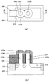
図46に特許文献1のSGTの(a)鳥瞰図および(b)断面構造を示す。これらの図を参照して、簡単にSGTについて説明する。シリコン基板上に柱状シリコン層1601が形成され、柱状シリコン層1601を取り囲むようにゲート絶縁膜1602が形成され、ゲート絶縁膜1602を取り囲むようにゲート電極1603が形成されている。柱状シリコン層1601の上下には、下部拡散層1604と上部拡散層1605が形成されている。上部拡散層1605はコンタクトを通して配線層1606へと接続される。
FIG. 46 shows (a) a bird's-eye view and (b) a cross-sectional structure of the SGT of
続いて、SGTを用いたCMOSインバーターの等価回路を図47(a)に、CMOSインバーターの平面図を(b)に、B−B’における断面図を(c)に示す。図47(b)、(c)を参照すると、Si基板1701上にNウェル1702およびPウェル1703が形成され、Si基板表面にはNウェル領域にPMOSを形成する柱状シリコン層1705が形成され、Pウェル領域にNMOSを形成する柱状シリコン層1706が形成され、それぞれの柱状シリコン層を取り囲むようにゲート1708が形成される。PMOSを形成する柱状半導体の底部に形成されるP+ドレイン拡散層1710およびNMOSを形成する柱状半導体の底部に形成されるN+ドレイン拡散層1712は出力端子Vout17に接続され、PMOSを形成する柱状シリコン層上部に形成されるソース拡散層1709は電源電位Vcc17に接続され、NMOSを形成する柱状シリコン層上部に形成されるソース拡散層1711は接地電位GND17に接続され、PMOSとNMOSの共通のゲート1708は入力端子Vin17に接続されることによりCMOSインバーターを形成する。
Subsequently, an equivalent circuit of a CMOS inverter using SGT is shown in FIG. 47A, a plan view of the CMOS inverter is shown in FIG. 47B, and a cross-sectional view taken along line BB ′ is shown in FIG. 47 (b) and 47 (c), an N well 1702 and a
SGTにおいてゲートによるチャネルの制御性を向上させて、ショートチャネル効果を十分に抑制するには、柱状シリコン層の寸法をゲート長に比べて十分に小さく形成しなければならない。柱状シリコン層の寸法を小さく形成するには、柱状シリコン層のドライエッチング時に寸法をシュリンクさせる方法や、柱状シリコン層形成後に犠牲酸化を行う方法などにより、比較的容易に寸法を縮小できる。このため、SGTでは十分にショートチャネル効果を抑制するために、シリコン柱の寸法は最小加工寸法Fより小さい寸法を持つことが多い。図48に柱状シリコン層1611の寸法が最小加工寸法Fより小さい場合のSGTの構造を示す。このSGTの構造においては、ゲート長が柱状シリコン層1611の寸法よりも十分長いためショートチャネル効果を抑制することができる。また柱状シリコン層上部に形成されるコンタクト1616は最小加工寸法F程度の大きさで形成されるため、柱状シリコン層1611よりも大きい構造になる。
In order to improve the controllability of the channel by the gate in the SGT and sufficiently suppress the short channel effect, the size of the columnar silicon layer must be formed sufficiently smaller than the gate length. In order to reduce the size of the columnar silicon layer, the size can be reduced relatively easily by a method of shrinking the size during dry etching of the columnar silicon layer or a method of performing sacrificial oxidation after forming the columnar silicon layer. For this reason, in SGT, in order to sufficiently suppress the short channel effect, the dimensions of the silicon pillar are often smaller than the minimum processing dimension F. FIG. 48 shows the structure of the SGT when the dimension of the
しかしながら、図48の構造を持つSGTにおいては、以下のような問題がある。第1に、SGTの寄生抵抗を低減するには、ピラー上部及び下部にシリサイド層を形成する必要があるが、柱状半導体層の寸法が小さくなると、シリサイドの細線効果により、ピラー上部にシリサイドを形成することが困難になる。また、ピラー上部にシリサイドが形成できたとしても、ピラー径が小さいため、シリサイドと上部拡散層の界面面積が小さくなり、シリサイドと上部拡散層の界面抵抗が大きく、トランジスタ特性を低下させてしまう。 However, the SGT having the structure of FIG. 48 has the following problems. First, in order to reduce the parasitic resistance of SGT, it is necessary to form silicide layers above and below the pillars. However, when the columnar semiconductor layer is reduced in size, silicide is formed above the pillars due to the fine line effect of silicide. It becomes difficult to do. Even if silicide can be formed on the upper part of the pillar, since the pillar diameter is small, the interface area between the silicide and the upper diffusion layer is reduced, the interface resistance between the silicide and the upper diffusion layer is increased, and the transistor characteristics are deteriorated.
第2に、SGTにおいては製造工程削減のため、柱状シリコン層の上部拡散層1415と下部の拡散層1614上に同時にコンタクトを形成することが望ましい。柱状シリコン層上部に形成されるコンタクト1616に対しては、下部の拡散層1614に形成されるコンタクトと比べると、柱状シリコン層の高さ以上のオーバーエッチが必要になる。図48のSGTの構造においては、柱状シリコン層上部に形成されるコンタクトにおいて、コンタクトエッチング時にオーバーエッチが過剰に行われることにより、ゲートとコンタクト間のショートが生じやすくなる。
Second, in SGT, it is desirable to form contacts on the
本発明は上記の事情を鑑みてなされたもので、縦型トランジスタにおいて、柱状シリコン層上部のシリサイドの細線効果を低減し、また、シリサイドと上部拡散層間の界面抵抗を低減することによりトランジスタ特性を改善することを目的とする。またコンタクトとゲート間のショートが発生しない構造を実現することを目的とする。 The present invention has been made in view of the above circumstances, and in a vertical transistor, transistor characteristics are reduced by reducing the thin-line effect of silicide above the columnar silicon layer and by reducing the interface resistance between the silicide and the upper diffusion layer. The goal is to improve. Another object of the present invention is to realize a structure in which a short circuit between the contact and the gate does not occur.
本発明の第1の態様は、柱状半導体層と、前記柱状半導体層の底部に形成される第1のドレイン又はソース領域と、該柱状半導体層の側壁を包囲するように第1の絶縁膜を介して形成されるゲート電極と、前記柱状半導体層上面上部に形成されるエピタキシャル半導体層とを含み、前記第2のソース又はドレイン領域が少なくとも前記エピタキシャル半導体層に形成され、前記第2のソース又はドレイン領域の上面の面積は、前記柱状半導体層の上面の面積よりも大きいことを特徴とするMOSトランジスタを提供するものである。 According to a first aspect of the present invention, a columnar semiconductor layer, a first drain or source region formed at the bottom of the columnar semiconductor layer, and a first insulating film so as to surround a sidewall of the columnar semiconductor layer are provided. A gate electrode formed on the columnar semiconductor layer and an epitaxial semiconductor layer formed on an upper surface of the columnar semiconductor layer, wherein the second source or drain region is formed in at least the epitaxial semiconductor layer, and the second source or The area of the upper surface of the drain region is larger than the area of the upper surface of the columnar semiconductor layer.
好ましくは、前記第2のドレイン又はソース領域の上面にシリサイド層が形成されている。 Preferably, a silicide layer is formed on the upper surface of the second drain or source region.
好ましくは、前記シリサイド層と、前記第2のドレイン又はソース領域との接触面積は前記柱状半導体層の上面の面積よりも大きい。 Preferably, the contact area between the silicide layer and the second drain or source region is larger than the area of the upper surface of the columnar semiconductor layer.
好ましくは、前記エピタキシャル半導体層は、n型の場合にはエピタキシャル成長によって成膜されたシリコン(Si)層、又はシリコンカーバイド(SiC)層であり、p型の場合にはエピタキシャル成長によって成膜されたシリコン(Si)層、又はシリコンゲルマニウム(SiGe)層である。 Preferably, the epitaxial semiconductor layer is a silicon (Si) layer or silicon carbide (SiC) layer formed by epitaxial growth in the case of n-type, and silicon formed by epitaxial growth in the case of p-type. It is a (Si) layer or a silicon germanium (SiGe) layer.
好ましくは、少なくとも2つの柱状半導体層から構成され、該少なくとも2つの柱状半導体層の上部に形成された前記エピタキシャル半導体層同士が互いに接続され、共通のソース又はドレイン領域となっている。 Preferably, the epitaxial semiconductor layer is composed of at least two columnar semiconductor layers, and the epitaxial semiconductor layers formed on the at least two columnar semiconductor layers are connected to each other to form a common source or drain region.
好ましくは、前記エピタキシャル半導体層は、第2の絶縁膜を介してゲート電極の上部に形成されている。 Preferably, the epitaxial semiconductor layer is formed on the gate electrode via the second insulating film.
好ましくは、前記シリサイド層上に形成されるコンタクトの面積が、前記シリサイド層の上面の面積よりも小さい。 Preferably, the area of the contact formed on the silicide layer is smaller than the area of the upper surface of the silicide layer.
好ましくは、前記少なくとも2つの柱状半導体層の上部に形成された前記エピタキシャル半導体層上に形成されるコンタクトの数が、前記柱状半導体層の数より少ない。 Preferably, the number of contacts formed on the epitaxial semiconductor layer formed above the at least two columnar semiconductor layers is smaller than the number of the columnar semiconductor layers.
好ましくは、少なくとも1つのコンタクトが前記互いに接続されたエピタキシャル半導体層上に形成され、該少なくとも1つのコンタクトは、前記互いに接続されたエピタキシャル半導体層上の、前記少なくとも2つの柱状半導体層のうちの一の柱状半導体層とそれに隣接する柱状半導体層との間に対応する位置に配置されるコンタクトを含む。 Preferably, at least one contact is formed on the mutually connected epitaxial semiconductor layers, and the at least one contact is one of the at least two columnar semiconductor layers on the mutually connected epitaxial semiconductor layers. And a contact disposed at a corresponding position between the columnar semiconductor layer and the columnar semiconductor layer adjacent thereto.
好ましくは、前記互いに接続されたエピタキシャル半導体層上に形成されるコンタクトのうちの少なくとも1つのコンタクトの前記基板の主面に平行な断面の面積の大きさが、他のコンタクトより大きい。 Preferably, at least one of the contacts formed on the epitaxial semiconductor layers connected to each other has a cross-sectional area parallel to the main surface of the substrate larger than that of the other contacts.
本発明の第2の態様は、上方に複数の柱状半導体層が形成された基板を用意する工程と、前記柱状半導体層の底部に第1のドレイン又はソース領域を形成する工程と、その後に表面に第1の絶縁膜を形成する工程と、前記第1の絶縁膜上に導電膜を形成する工程と、前記第1の絶縁膜及び前記導電膜をエッチバックし、前記柱状半導体層側面の前記第1の絶縁膜及び前記導電膜をゲート長の高さに形成する工程と、前記導電膜及び前記第1の絶縁膜を選択的にエッチングにより除去し、前記柱状半導体層の周囲に形成されたゲート電極及び該ゲート電極から延在するゲート配線を形成する工程と、前記複数の柱状半導体層の少なくとも1つの上面上部に、その上面の面積が前記柱状半導体層の上面の面積よりも大きいエピタキシャル層を形成する工程と、前記エピタキシャル層と前記柱状半導体層に、前記基板上に形成された第1のドレイン又はソース領域と同じ導電型の第2のソース又はドレイン領域を形成する工程とを含むことを特徴とするMOSトランジスタを備えた半導体装置の製造方法を提供するものである。 According to a second aspect of the present invention, a step of preparing a substrate having a plurality of columnar semiconductor layers formed thereon, a step of forming a first drain or source region at the bottom of the columnar semiconductor layer, and a surface thereafter Forming a first insulating film on the first insulating film; forming a conductive film on the first insulating film; etching back the first insulating film and the conductive film; Forming a first insulating film and the conductive film at a gate length; and selectively removing the conductive film and the first insulating film by etching to form a periphery of the columnar semiconductor layer; A step of forming a gate electrode and a gate wiring extending from the gate electrode; and an epitaxial layer having an upper surface area larger than an upper surface area of the columnar semiconductor layer on an upper surface of at least one of the plurality of columnar semiconductor layers Forming And forming a second source or drain region of the same conductivity type as the first drain or source region formed on the substrate in the epitaxial layer and the columnar semiconductor layer. A method for manufacturing a semiconductor device including a MOS transistor is provided.
好ましくは、前記エピタキシャル層の表面にシリサイド層を形成する工程を更に含む。 Preferably, the method further includes a step of forming a silicide layer on the surface of the epitaxial layer.
好ましくは、前記エピタキシャル半導体層は、n型の場合にはエピタキシャル成長によって成膜されたシリコン(Si)層、又はシリコンカーバイド(SiC)層であり、p型の場合にはエピタキシャル成長によって成膜されたシリコン(Si)層、又はシリコンゲルマニウム(SiGe)層である。 Preferably, the epitaxial semiconductor layer is a silicon (Si) layer or silicon carbide (SiC) layer formed by epitaxial growth in the case of n-type, and silicon formed by epitaxial growth in the case of p-type. It is a (Si) layer or a silicon germanium (SiGe) layer.
好ましくは、エピタキシャル成長の成膜条件を調整することにより、所定の間隔以下で隣接するMOSトランジスタを構成する複数の前記柱状半導体層に対してのみ、MOSトランジスタを構成する複数の前記柱状半導体層の上面上部に形成される前記エピタキシャル層の少なくとも2つは、自己整合的に互いに接続され、共通のソース又はドレイン領域となるように形成される。 Preferably, by adjusting the film formation conditions for epitaxial growth, the upper surfaces of the plurality of columnar semiconductor layers constituting the MOS transistor only for the plurality of columnar semiconductor layers constituting the adjacent MOS transistors at a predetermined interval or less. At least two of the epitaxial layers formed on the top are connected to each other in a self-aligned manner so as to be a common source or drain region.
好ましくは、前記エピタキシャル層を形成する工程の前処理として、前記ゲート電極と、前記エピタキシャル半導体層とを分離するための第2の絶縁膜を形成する工程を更に含む。 Preferably, as a pretreatment of the step of forming the epitaxial layer, a step of forming a second insulating film for separating the gate electrode and the epitaxial semiconductor layer is further included.
好ましくは、前記第2の絶縁膜を形成する工程は、表面にシリコン窒化膜又はシリコン窒化膜とシリコン酸化膜の積層膜を形成する工程と、前記シリコン窒化膜又はシリコン窒化膜とシリコン酸化膜の積層膜を、前記ゲート電極上部のシリコン窒化膜又はシリコン窒化膜とシリコン酸化膜の積層膜が存在するように、且つ前記第1のドレイン又はソース領域及び前記柱状半導体層の上面を露出させるように、エッチバックし、前記柱状半導体層の側壁及び前記ゲート電極壁面及び前記ゲート配線壁面を前記シリコン窒化膜又はシリコン窒化膜とシリコン酸化膜の積層膜で覆う工程とを更に含む。 Preferably, the step of forming the second insulating film includes a step of forming a silicon nitride film or a stacked film of a silicon nitride film and a silicon oxide film on the surface, and a step of forming the silicon nitride film or the silicon nitride film and the silicon oxide film. The stacked film is formed so that a silicon nitride film or a stacked film of a silicon nitride film and a silicon oxide film on the gate electrode exists, and the top surface of the first drain or source region and the columnar semiconductor layer is exposed. Etching back and covering the sidewall of the columnar semiconductor layer, the wall surface of the gate electrode, and the wall surface of the gate wiring with the silicon nitride film or a laminated film of the silicon nitride film and the silicon oxide film.
好ましくは、前記上方に複数の柱状半導体層が形成された基板を用意する工程及び前記柱状半導体層の下部に第1のドレイン又はソース領域を形成する工程は、基板上に複数の柱状半導体層を形成する工程と、前記基板上に素子分離を形成する工程と、前記基板上に第1のドレイン又はソース領域を形成する工程とからなる。 Preferably, the step of preparing the substrate on which the plurality of columnar semiconductor layers are formed and the step of forming the first drain or source region below the columnar semiconductor layer include the step of forming the plurality of columnar semiconductor layers on the substrate. Forming a step, forming an element isolation on the substrate, and forming a first drain or source region on the substrate.
好ましくは、前記上方に複数の柱状半導体層が形成された基板を用意する工程及び前記柱状半導体層の下部に第1のドレイン又はソース領域を形成する工程は、基板上の絶縁膜上に平面状半導体層及び該平面状半導体層上の複数の柱状半導体層を形成する工程と、 前記平面状半導体層を素子に分離する工程と、前記平面状半導体層に第1のドレイン又はソース領域を形成する工程とからなる。 Preferably, the step of preparing a substrate on which a plurality of columnar semiconductor layers are formed and the step of forming a first drain or source region below the columnar semiconductor layer are planar on an insulating film on the substrate. Forming a semiconductor layer and a plurality of columnar semiconductor layers on the planar semiconductor layer; isolating the planar semiconductor layer into elements; and forming a first drain or source region in the planar semiconductor layer. Process.
ここで、基板の「上方」とは、基板上又は基板上に形成された何らかの層を介した基板の上方をいう。 Here, “above” the substrate means above the substrate via a substrate or some layer formed on the substrate.
本発明によれば、縦型トランジスタにおいて、柱状シリコン層上部のシリサイドの細線効果を低減することができる。また、シリサイドと上部拡散層間の界面抵抗を低減することによりトランジスタ特性を改善することができる。また、コンタクトとゲート間のショートが発生しない構造を実現することができる。 According to the present invention, it is possible to reduce the thin line effect of silicide on the columnar silicon layer in the vertical transistor. Further, the transistor characteristics can be improved by reducing the interface resistance between the silicide and the upper diffusion layer. Further, it is possible to realize a structure in which a short circuit between the contact and the gate does not occur.
〔実施例1〕
図1は本発明を用いたトランジスタの平面図及びA−A’の断面図である。以下に、図1のトランジスタの平面図及びA−A’の断面図を用いて本実施例について説明する。シリコン基板101は素子分離102により分離され、シリコン基板上には柱状シリコン層(柱状半導体層)(105a、105b)が形成されている。柱状シリコン層(柱状半導体層)の周囲にはゲート絶縁膜(第1の絶縁膜)107及びゲート電極(108a、108b)が形成されている。本実施例においてはゲート絶縁膜(第1の絶縁膜)としてはHigh−k膜、ゲート電極としては金属膜を用いているが、ゲート絶縁膜(第1の絶縁膜)としては酸化によるシリコン酸窒化膜、ゲート電極としてはポリシリコン等も用いることが出来る。柱状シリコン層(柱状半導体層)の底部には下部N+拡散層(第1のドレイン又はソース領域)103が形成され、下部N+拡散層(第1のドレイン又はソース領域)103の表面には、寄生抵抗を低減するために下部シリサイド層111aが形成されている。柱状シリコン層(柱状半導体層)の上部には上面積が柱状半導体層より大きい上部N+拡散層(第2のソース又はドレイン領域)(109a、109b)が形成されている。本実施例では、この上面積が柱状半導体層より大きい上部拡散層(109a、109b)は、その上の部分がエピタキシャルシリコン成長により形成された半導体エピタキシャル層、その下の部分が柱状半導体層の上の部分から構成されている。上部N+拡散層(第2のソース又はドレイン領域)(109a、109b)は、半導体エピタキシャル層の一部又は全部から構成されてもよい。半導体エピタキシャル層は、シリコン窒化膜又はシリコン窒化膜とシリコン酸化膜の積層膜等の第2の絶縁膜112を介してゲート電極(108a、108b)と絶縁されている。上部N+拡散層(第2のソース又はドレイン領域)(109a、109b)にはシリサイド層(111b、111c)が形成されるが、このシリサイド層は柱状シリコン層(柱状半導体層)の径より大きいエピタキシャルシリコン層(半導体エピタキシャル層)上に形成されるため、シリサイドの細線効果の影響を低減することができる。また、シリサイドと拡散層の界面の面積を大きく取れるため、シリサイドと拡散層間の界面抵抗を低減することができる。また、柱状シリコン層(柱状半導体層)上部に形成されるコンタクト(115、116)について、上部N+拡散層(第2のソース又はドレイン領域)の上面に形成されたシリサイド層(111b、111c)をコンタクト(115、116)の径より大きく形成する場合には、コンタクトエッチング時にオーバーエッチを行っても、コンタクトとゲートがショートするのを防止することができる。柱状シリコン層(柱状半導体層)上部に形成されるコンタクト(115、116)は配線層120を通して一方のソースドレイン端子に接続され、柱状シリコン層(柱状半導体層)下部に形成されるコンタクト118は配線層122を通して他方のソースドレイン端子に接続され、ゲート電極から延在するゲート配線108上に形成されるコンタクト117は配線層121を通してゲート端子に接続される。
[Example 1]
FIG. 1 is a plan view of a transistor using the present invention and a cross-sectional view taken along line AA ′. Hereinafter, this embodiment will be described with reference to a plan view of the transistor in FIG. 1 and a cross-sectional view taken along line AA ′. The
図2のように、隣接する柱状シリコン層(柱状半導体層)(205a、205b)間の距離が所定の距離より近い場合には、エピタキシャル成長膜厚を調整することにより、隣接する柱状半導体層の上部N+拡散層(第2のソース又はドレイン領域)を自己整合的に接続することができる。この場合、柱状シリコン層(柱状半導体層)上部のシリサイド層211bと上部N+拡散層(第2のソース又はドレイン領域)(209a、209b)との界面面積がより大きくなるため、さらにシリサイドと上部N+拡散層(第2のソース又はドレイン領域)間の界面抵抗を低減することができる。また、柱状シリコン層(柱状半導体層)上部のシリサイド層211bの面積が大きくなるため、シリサイドの細線効果の影響が大きく低減し、シリサイドの形成が容易になる。
When the distance between adjacent columnar silicon layers (columnar semiconductor layers) (205a, 205b) is closer than a predetermined distance as shown in FIG. 2, the epitaxial growth film thickness is adjusted to adjust the upper portion of the adjacent columnar semiconductor layer. The N + diffusion layer (second source or drain region) can be connected in a self-aligning manner. In this case, since the interface area between the
図3のように複数の柱状シリコン層(柱状半導体層)に対して、柱状シリコン層(柱状半導体層)の数より少ない個数のコンタクトにて複数の柱状シリコン層(柱状半導体層)上部と配線層を接続することもできる。 As shown in FIG. 3, with respect to a plurality of columnar silicon layers (columnar semiconductor layers), upper portions of the plurality of columnar silicon layers (columnar semiconductor layers) and wiring layers with a smaller number of contacts than the number of columnar silicon layers (columnar semiconductor layers). Can also be connected.
更に、図4のようにコンタクト415を、接続された上部N+拡散層(第2のソース又はドレイン領域)(409a、409b)上の、柱状シリコン層(柱状半導体層)間に対応する位置に配置することもできる。ここで、コンタクト415は、コンタクト415の軸が、柱状シリコン層(柱状半導体層)の軸と軸を結ぶ線分上のみならず、柱状シリコン層(柱状半導体層)の軸と軸との間の領域に位置すればよい。この構成により、配線層420と他の配線(421、422)間のスペースを大きくとることができるので、配線の引き回しを容易にすることができる。
Further, as shown in FIG. 4, the
また、図5のように、基板の主面に平行な断面の面積が他のコンタクト(517,518)よりも大きいコンタクト515を、複数の柱状シリコン層(柱状半導体層)上に柱状シリコン層(柱状半導体層)の個数より少ない個数形成することにより、コンタクト抵抗を低減したり、安定してコンタクトを形成することができる。
Further, as shown in FIG. 5, a
以下に本発明の図2の半導体装置を形成するための製造方法の一例を図6〜図20を参照して説明する。各図において(a)は平面図、(b)はA−A’の断面図を示している。 An example of a manufacturing method for forming the semiconductor device of FIG. 2 according to the present invention will be described below with reference to FIGS. In each figure, (a) is a plan view and (b) is a cross-sectional view taken along line A-A ′.
図6に示されるように、基板201上にシリコン窒化膜等のハードマスク層204a及び、柱状シリコン層(柱状半導体層)(205a、205b)をリソグラフィー及びエッチングにより形成する。
As shown in FIG. 6, a
図7に示されるように、基板上に素子分離202を形成する。素子分離は、まず溝パターンをエッチングして、シリカなどの塗布やCVDにより溝パターンに酸化膜を埋め込み、余分な基板上の酸化膜をドライエッチやウェットエッチなどにより取り除くことにより形成する。
As shown in FIG. 7,
図8に示されるように、素子分離202形成後、イオン注入などにより柱状シリコン層(柱状半導体層)の下部拡散層203を形成する。このとき、柱状シリコン層(柱状半導体層)上部のハードマスク層204aにより柱状シリコン層(柱状半導体層)(205a、205b)には不純物が注入されないようにする。
As shown in FIG. 8, after the
図9に示されるように、ゲート絶縁膜(第1の絶縁膜)207及びゲート導電膜208cを成膜する。ゲート絶縁膜(第1の絶縁膜)207は酸化膜やHigh−k膜等により形成される。また、ゲート導電膜208cはポリシリコンや金属膜等により形成される。
As shown in FIG. 9, a gate insulating film (first insulating film) 207 and a gate
図10に示されるように、ゲート導電膜208cをCMP等により平坦化する。
As shown in FIG. 10, the gate
図11に示されるように、ゲート絶縁膜(第1の絶縁膜)207及びゲート導電膜208cをエッチバックし、柱状シリコン層(柱状半導体層)(205a、205b)側面のゲート絶縁膜(第1の絶縁膜)207及びゲート導電膜208cを所望のゲート長に設定する。
As shown in FIG. 11, the gate insulating film (first insulating film) 207 and the gate
図12に示されるように、窒化膜等を成膜しエッチバックすることにより、サイドウォールスペーサー204bを形成する。
As shown in FIG. 12, a
図13に示されるように、リソグラフィー等を用いてレジスト210によりゲート配線パターンをパターニングする。 As shown in FIG. 13, the gate wiring pattern is patterned by a resist 210 using lithography or the like.
図14に示されるように、レジスト210をマスクに用いてゲート導電膜208c及びゲート絶縁膜(第1の絶縁膜)207を異方性エッチング等により選択的にエッチングして、柱状シリコン層(柱状半導体層)(205a、205b)の周囲にゲート電極(208a、208b)、及びゲート電極(208a、208b)から延在するゲート電極(208)を形成する。その後レジスト210を除去する。
As shown in FIG. 14, the gate
図15に示されるように、ハードマスク204a及びサイドウォールスペーサー204bをウェットエッチング等により除去する。
As shown in FIG. 15, the
図16に示されるように、窒化膜や窒化膜と酸化膜との積層膜などを成膜してエッチバックすることにより第2の絶縁膜212を形成する。
As shown in FIG. 16, a second
図17に示されるように、シリコン等を柱状シリコン層(柱状半導体層)の上面上部と下部の拡散層上に選択的にエピタキシャル成長させて、所定の間隔より近くに隣接する柱状シリコン層(柱状半導体層)の上面上部に形成されるエピタキシャル層が互いに接続されるようにエピタキシャルシリコン層(半導体エピタキシャル層)210bを自己整合的に形成する。また、エピタキシャルシリコン層(半導体エピタキシャル層)の径が後工程で形成される柱状シリコン層(柱状半導体層)上に形成されるコンタクトの径よりも大きく形成する場合には、コンタクトとゲート間がショートしない構造にすることができる。 As shown in FIG. 17, silicon or the like is selectively epitaxially grown on the upper and lower diffusion layers of a columnar silicon layer (columnar semiconductor layer), and adjacent columnar silicon layers (columnar semiconductors) closer than a predetermined distance. The epitaxial silicon layer (semiconductor epitaxial layer) 210b is formed in a self-aligning manner so that the epitaxial layers formed on the upper surface of the layer are connected to each other. Further, when the diameter of the epitaxial silicon layer (semiconductor epitaxial layer) is larger than the diameter of the contact formed on the columnar silicon layer (columnar semiconductor layer) formed in a later step, the contact and the gate are short-circuited. The structure can not be.
図18に示されるように、イオン注入などにより、エピタキシャルシリコン層(半導体エピタキシャル層)210b及び柱状シリコン層(柱状半導体層)(205a、205b)の上の部分に上部N+拡散層(第2のソース又はドレイン領域)(209a、209b)を形成する。なお、上部N+拡散層(第2のソース又はドレイン領域)が形成される領域は、エピタキシャルシリコン層(半導体エピタキシャル層)210bの一部又は全部のみであってもよい。 As shown in FIG. 18, the upper N + diffusion layer (second source) is formed on the epitaxial silicon layer (semiconductor epitaxial layer) 210b and the columnar silicon layers (columnar semiconductor layers) (205a, 205b) by ion implantation or the like. (Or drain region) (209a, 209b). Note that the region where the upper N + diffusion layer (second source or drain region) is formed may be only part or all of the epitaxial silicon layer (semiconductor epitaxial layer) 210b.
図19に示されるように、CoやNiなどの金属をスパッタして、熱処理を行うことにより、上部N+拡散層(第2のソース又はドレイン領域)を選択的にシリサイド化して、下部シリサイド層211aおよび上部シリサイド層211bを形成する。上部シリサイド層211bは柱状シリコン層(柱状半導体層)の寸法より大きく形成されるため、シリサイドの細線効果を抑制することができる。また、エピタキシャルシリコン層(半導体エピタキシャル層)の上面全体をシリサイド化エピタキシャルシリコン層(半導体エピタキシャル層)すると、上部シリサイド層211bと上部拡散層(209a、209b)との接触面積が柱状シリコン層(柱状半導体層)の上面より大きくなるため、界面抵抗が減少し、ソースドレイン寄生抵抗を低減することができる。
As shown in FIG. 19, the upper N + diffusion layer (second source or drain region) is selectively silicided by sputtering a metal such as Co or Ni and performing a heat treatment, so that the
図20に示されるように、層間膜であるシリコン酸化膜形成後にコンタクト(215〜218)を形成する。このときに、図20のように柱状シリコン層(柱状半導体層)上部に形成されるコンタクト(215、216)が、完全に上部シリサイド層211b上に形成されるようにエピタキシャルシリコン層(半導体エピタキシャル層)を形成すると、コンタクトの形成時にオーバーエッチが行われても、コンタクトとゲート間のショートは発生しない構造になる。
As shown in FIG. 20, contacts (215 to 218) are formed after forming a silicon oxide film as an interlayer film. At this time, as shown in FIG. 20, the epitaxial silicon layer (semiconductor epitaxial layer) is formed so that the contacts (215, 216) formed on the columnar silicon layer (columnar semiconductor layer) are completely formed on the
本実施例においてはエピタキシャルシリコン層(半導体エピタキシャル層)を形成した場合を示しているが、NMOSにはエピタキシャルシリコンカーバイド(SiC)層を、PMOSにはエピタキシャルシリコンゲルマニウム(SiGe)層を形成することにより、チャネル部に応力を加えて、移動度を向上させることも可能である。 In this embodiment, an epitaxial silicon layer (semiconductor epitaxial layer) is formed, but by forming an epitaxial silicon carbide (SiC) layer for NMOS and an epitaxial silicon germanium (SiGe) layer for PMOS. It is also possible to improve mobility by applying stress to the channel portion.
〔実施例2〕
本実施例は本発明を2個直列に接続したトランジスタに適用した実施例である。図21は本実施例の平面図及びA−A’の断面図である。以下に、図21のトランジスタの平面図及びA−A’の断面図について説明する。シリコン基板601は素子分離602により分離され、シリコン基板上には第1のトランジスタを形成する柱状シリコン層(柱状半導体層)(605a、605b)及び第2のトランジスタを形成する柱状シリコン層(柱状半導体層)(605c、605d)が形成されている。柱状シリコン層(柱状半導体層)の周囲にはゲート絶縁膜(第1の絶縁膜)607及びゲート電極(609a〜609d)が形成されている。本実施例においてはゲート絶縁膜(第1の絶縁膜)としてはHigh−k膜、ゲート電極としては金属膜を用いているが、ゲート絶縁膜(第1の絶縁膜)としては酸化によるシリコン酸窒化膜、ゲート電極としてはポリシリコン等も用いることが出来る。柱状シリコン層(柱状半導体層)の底部には下部N+拡散層(第1のドレイン又はソース領域)603が形成され、下部N+拡散層(第1のドレイン又はソース領域)603の表面には、寄生抵抗を低減するために下部シリサイド層611aが形成されている。柱状シリコン層(柱状半導体層)の上部には上面積が柱状半導体層より大きい上部N+拡散層(第2のソース又はドレイン領域)(609a〜609d)が形成されている。本実施例では、この上面積が柱状半導体層より大きい上部N+拡散層(第2のソース又はドレイン領域)は、その上の部分がエピタキシャルシリコン成長により形成された半導体エピタキシャル層、その下の部分が柱状半導体層の上の部分から構成されている。上部N+拡散層(第2のソース又はドレイン領域)は、半導体エピタキシャル層の一部又は全部のみから構成されてもよい。半導体エピタキシャル層は、シリコン窒化膜又はシリコン窒化膜とシリコン酸化膜の積層膜などの第2の絶縁膜612を介してゲート電極(609a〜609d)と絶縁されている。このときに、第1のトランジスタを形成する2個の柱状シリコン層(柱状半導体層)(605a、605b)は近くに形成されているため、柱状シリコン層(柱状半導体層)の上面上部のエピタキシャルシリコン層(半導体エピタキシャル層)は自己整合的に接続される。同様に、第2のトランジスタを形成する2個の柱状シリコン層(柱状半導体層)(605c、605d)も近くに形成されているため、柱状シリコン層(柱状半導体層)の上面上部のエピタキシャルシリコン層(半導体エピタキシャル層)は自己整合的に接続される。一方、異なるトランジスタを形成する柱状シリコン層(柱状半導体層)である605bと605cは一定の間隔以上の間隔をあけて配置されているため、エピタキシャルシリコン層(半導体エピタキシャル層)は分離される。
[Example 2]
In this embodiment, the present invention is applied to two transistors connected in series. FIG. 21 is a plan view of this embodiment and a cross-sectional view taken along line AA ′. Hereinafter, a plan view of the transistor in FIG. 21 and a cross-sectional view along AA ′ will be described. The
上部N+拡散層(第2のソース又はドレイン領域)(609a〜609d)上にはシリサイド層(611b、611c)が形成されるが、このシリサイド層は柱状シリコン層(柱状半導体層)の径より大きいエピタキシャルシリコン層(半導体エピタキシャル層)上に形成されるため、シリサイドの細線効果の影響を低減することができる。また、シリサイドと拡散層の界面の面積を大きく取れるため、シリサイド(611b、611c)と上部N+拡散層(第2のソース又はドレイン領域)(609a〜609d)間の界面抵抗を低減することができる。また、柱状シリコン層(柱状半導体層)上部に形成されるコンタクト(615a、615b、615a、616b)について、上部N+拡散層(第2のソース又はドレイン領域)の上面に形成されたシリサイド層(611b、611c)をコンタクト(615a、615b、615a、616b)の径より大きく形成する場合には、コンタクトエッチング時にオーバーエッチを行っても、コンタクトとゲートがショートするのを防止することができる。第1のトランジスタを形成する柱状シリコン層(柱状半導体層)上部に形成されるコンタクト(615a、615b)は配線層620aを通して一方のソースドレイン端子に接続され、第2のトランジスタを形成する柱状シリコン層(柱状半導体層)上部に形成されるコンタクト(616a、616b)は配線層620bを通して他方のソースドレイン端子に接続され、第1のトランジスタと第2のトランジスタは下部N+拡散層(第1のドレイン又はソース領域)603により直列に接続される。また、ゲート電極から延在するゲート配線608上に形成されるコンタクト617は配線層621を通してゲート端子に接続される。
Silicide layers (611b and 611c) are formed on the upper N + diffusion layer (second source or drain region) (609a to 609d), and this silicide layer is larger than the diameter of the columnar silicon layer (columnar semiconductor layer). Since it is formed on the epitaxial silicon layer (semiconductor epitaxial layer), it is possible to reduce the influence of the fine line effect of silicide. Further, since the area of the interface between the silicide and the diffusion layer can be increased, the interface resistance between the silicide (611b, 611c) and the upper N + diffusion layer (second source or drain region) (609a to 609d) can be reduced. . Further, with respect to the contacts (615a, 615b, 615a, 616b) formed on the columnar silicon layer (columnar semiconductor layer), a silicide layer (611b) formed on the upper surface of the upper N + diffusion layer (second source or drain region). , 611c) is formed larger than the diameter of the contact (615a, 615b, 615a, 616b), it is possible to prevent the contact and the gate from being short-circuited even if overetching is performed during contact etching. The contacts (615a, 615b) formed on the columnar silicon layer (columnar semiconductor layer) forming the first transistor are connected to one source / drain terminal through the
図22のように複数の柱状シリコン層(柱状半導体層)に対して、柱状シリコン層(柱状半導体層)の数より少ない個数のコンタクトにて複数の柱状シリコン層(柱状半導体層)上部と配線層を接続することもできる。 As shown in FIG. 22, with respect to a plurality of columnar silicon layers (columnar semiconductor layers), upper portions of the plurality of columnar silicon layers (columnar semiconductor layers) and wiring layers with a smaller number of contacts than the number of columnar silicon layers (columnar semiconductor layers). Can also be connected.
例えば、図22のようにコンタクト(715、716)を、接続された上部N+拡散層(第2のソース又はドレイン領域)(711b、711c)上の、柱状シリコン層(柱状半導体層)間に対応する位置に配置することもできる。ここで、コンタクト(715、716)は、コンタクト(715、716)の軸が、柱状シリコン層(柱状半導体層)の軸と軸を結ぶ線分上のみならず、柱状シリコン層(柱状半導体層)の軸と軸との間の領域に位置すればよい。この構成により、配線層(720a、720b、721)間のスペースを大きくすることができるので、配線の引き回しを容易にすることができる。 For example, as shown in FIG. 22, the contacts (715, 716) correspond to the columnar silicon layers (columnar semiconductor layers) on the connected upper N + diffusion layers (second source or drain regions) (711b, 711c). It can also be arranged at the position to be. Here, the contact (715, 716) is not only on the line segment connecting the axis of the contact (715, 716) and the axis of the columnar silicon layer (columnar semiconductor layer), but also the columnar silicon layer (columnar semiconductor layer). It suffices to be located in a region between the axes. With this configuration, the space between the wiring layers (720a, 720b, and 721) can be increased, so that the wiring can be easily routed.
また、図5の場合と同様に、基板の主面に平行な断面の面積が他のコンタクトよりも大きいコンタクトを、複数の柱状シリコン層(柱状半導体層)上に柱状シリコン層(柱状半導体層)の個数より少ない個数形成することにより、コンタクト抵抗を低減したり、安定してコンタクトを形成することができる。 Similarly to the case of FIG. 5, a contact having a larger cross-sectional area parallel to the main surface of the substrate than other contacts is formed on a plurality of columnar silicon layers (columnar semiconductor layers) as columnar silicon layers (columnar semiconductor layers). By forming the number smaller than the number of contacts, the contact resistance can be reduced or the contact can be stably formed.
〔実施例3〕
本実施例は本発明をCMOSインバーターに適用した実施例である。図23は本実施例の平面図及びA−A’の断面図である。図23において、NMOSに接続する配線層820aはGNDに接続され、PMOSに接続する配線層820bはVccに接続される。ゲート配線層808には配線層822より入力信号(Vin)が入力され、NMOS及びPMOSの上部より接続される配線層である821aと821bは配線層にて接続され出力信号(Vout)が出力されることにより、CMOSインバーターが形成される。
Example 3
In this embodiment, the present invention is applied to a CMOS inverter. FIG. 23 is a plan view of this embodiment and a cross-sectional view taken along line AA ′. In FIG. 23, a
以下に、図23のCMOSインバーターの平面図及びA−A’の断面図について説明する。シリコン基板801は素子分離802により分離され、シリコン基板上にはNMOSを形成する2個の柱状シリコン層(柱状半導体層)805a及びPMOSを形成する4個の柱状シリコン層(柱状半導体層)805bが形成されている。それぞれの柱状シリコン層(柱状半導体層)の周囲にはゲート絶縁膜(第1の絶縁膜)807及びゲート電極(808a、808b)が形成されている。本実施例においてはゲート絶縁膜(第1の絶縁膜)としてはHigh−k膜、ゲート電極としては金属膜を用いているが、ゲート絶縁膜(第1の絶縁膜)としては酸化によるシリコン酸窒化膜、ゲート電極としてはポリシリコン等も用いることが出来る。NMOSを形成する柱状シリコン層(柱状半導体層)805aの底部にはPウェル801aに囲まれた下部N+拡散層(第1のドレイン又はソース領域)803aが形成され、PMOSを形成する柱状シリコン層(柱状半導体層)805bの底部にはNウェル801bに囲まれた下部P+拡散層803bが形成され、下部P+拡散層(第1のドレイン又はソース領域)の表面には、寄生抵抗を低減するために下部シリサイド層(811a、811b)が形成されている。NMOSを形成する柱状シリコン層(柱状半導体層)805aの上部には柱状半導体層より大きい上部N+拡散層(第2のソース又はドレイン領域)809aが形成されており、PMOSを形成する柱状シリコン層(柱状半導体層)805bの上部には柱状半導体層より大きい上部P+拡散層809bが形成されている。本実施例では、この上面積が柱状半導体層より大きい上部拡散層は、その上の部分がエピタキシャルシリコン成長により形成された半導体エピタキシャル層、その下の部分が柱状半導体層の上の部分から構成されている。上部拡散層は、半導体エピタキシャル層の一部又は全部のみから構成されていてもよい。半導体エピタキシャル層は、シリコン窒化膜又はシリコン窒化膜とシリコン酸化膜の積層膜などの第2の絶縁膜812を介してゲート電極(808a、808b)と絶縁されている。このときに、NMOSを形成する2個の柱状シリコン層(柱状半導体層)805aは近くに形成されているため、柱状シリコン層(柱状半導体層)上部のエピタキシャルシリコン層(半導体エピタキシャル層)は自己整合的に接続され、PMOSを形成する4個の柱状シリコン層(柱状半導体層)805bは近くに形成されているため、柱状シリコン層(柱状半導体層)上部のエピタキシャルシリコン層(半導体エピタキシャル層)は自己整合的に接続される。
Hereinafter, a plan view of the CMOS inverter of FIG. 23 and a cross-sectional view of A-A ′ will be described. The
上部拡散層(809a、809b)上にはシリサイド層(811c、811d)が形成されるが、このシリサイド層は柱状シリコン層(柱状半導体層)の径より大きいエピタキシャルシリコン層(半導体エピタキシャル層)上に形成されるため、シリサイドの細線効果の影響を低減することができる。また、シリサイド(811c、811d)と拡散層(809a、809b)の界面の面積を大きく取れるため、シリサイドと拡散層間の界面抵抗を低減することができる。また、柱状シリコン層(柱状半導体層)上部に形成されるコンタクト(815、816)について、上部N+拡散層(第2のソース又はドレイン領域)の上面に形成されたシリサイド層(811c、811d)をコンタクト(815、816)の径より大きく形成する場合には、コンタクトエッチング時にオーバーエッチを行っても、コンタクトとゲートがショートするのを防止することができる。図24のように複数の柱状シリコン層(柱状半導体層)に対して、柱状シリコン層(柱状半導体層)の数より少ない個数のコンタクトにて複数の柱状シリコン層(柱状半導体層)上部と配線層を接続することもできる。 Silicide layers (811c, 811d) are formed on the upper diffusion layers (809a, 809b). The silicide layers are formed on an epitaxial silicon layer (semiconductor epitaxial layer) larger than the diameter of the columnar silicon layer (columnar semiconductor layer). Since it is formed, the influence of the fine line effect of silicide can be reduced. Further, since the area of the interface between the silicide (811c, 811d) and the diffusion layer (809a, 809b) can be increased, the interface resistance between the silicide and the diffusion layer can be reduced. For the contacts (815, 816) formed on the upper part of the columnar silicon layer (columnar semiconductor layer), silicide layers (811c, 811d) formed on the upper surface of the upper N + diffusion layer (second source or drain region) are provided. When the contact is formed larger than the diameter of the contact (815, 816), it is possible to prevent the contact and the gate from being short-circuited even if overetching is performed during contact etching. As shown in FIG. 24, with respect to the plurality of columnar silicon layers (columnar semiconductor layers), the upper portions of the plurality of columnar silicon layers (columnar semiconductor layers) and the wiring layers are formed by a smaller number of contacts than the number of columnar silicon layers (columnar semiconductor layers). Can also be connected.
更に、図24におけるNMOSのようにコンタクト915を、接続された上部N+拡散層(第2のソース又はドレイン領域)(909a)上の、柱状シリコン層(柱状半導体層)間に対応する位置に配置することもできる。ここで、コンタクト915は、コンタクト915の軸が、柱状シリコン層(柱状半導体層)の軸と軸を結ぶ線分上のみならず、柱状シリコン層(柱状半導体層)の軸と軸との間の領域に位置すればよい。この構成や図24におけるPMOSのようにコンタクトの個数を減らしたりすることで、配線層(920a、920b、921a、921b、922)間のスペースを大きくことができるので、配線の引き回しを容易にすることができる。
Further, like the NMOS in FIG. 24, the
また、図5の場合と同様に、基板の主面に平行な断面の面積が他のコンタクトよりも大きいコンタクトを、複数の柱状シリコン層(柱状半導体層)上に柱状シリコン層(柱状半導体層)の個数より少ない個数形成することにより、コンタクト抵抗を低減したり、安定してコンタクトを形成することができる。 Similarly to the case of FIG. 5, a contact having a larger cross-sectional area parallel to the main surface of the substrate than other contacts is formed on a plurality of columnar silicon layers (columnar semiconductor layers) as columnar silicon layers (columnar semiconductor layers). By forming the number smaller than the number of contacts, the contact resistance can be reduced or the contact can be stably formed.
〔実施例4〕
図25はSOI基板を用いた場合における本発明のトランジスタの平面図及びA−A’の断面図である。以下に、図1のトランジスタの平面図及びA−A’の断面図を用いて本実施例について説明する。SOI基板上のシリコン層1002は素子ごとに分離され、シリコン層1002上には柱状シリコン層(柱状半導体層)(1005a、1005b)が形成されている。柱状シリコン層(柱状半導体層)の周囲にはゲート絶縁膜(第1の絶縁膜)1007及びゲート電極(1008a、1008b)が形成されている。本実施例においてはゲート絶縁膜(第1の絶縁膜)としてはHigh−k膜、ゲート電極としては金属膜を用いているが、ゲート絶縁膜(第1の絶縁膜)としては酸化によるシリコン酸窒化膜、ゲート電極としてはポリシリコン等も用いることが出来る。柱状シリコン層(柱状半導体層)の底部には下部N+拡散層(第1のドレイン又はソース領域)1003が形成され、下部N+拡散層(第1のドレイン又はソース領域)1003の表面には、寄生抵抗を低減するために下部シリサイド層1011aが形成されている。柱状シリコン層(柱状半導体層)の上部には上面積が柱状半導体層より大きい上部N+拡散層(第2のソース又はドレイン領域)(1009a、1009b)が形成されている。本実施例では、この上面積が柱状半導体層より大きい上部N+拡散層(第2のソース又はドレイン領域)は、その上の部分がエピタキシャルシリコン成長により形成された半導体エピタキシャル層、その下の部分が柱状半導体層の上の部分から構成されている。上部N+拡散層(第2のソース又はドレイン領域)は、半導体エピタキシャル層の一部又は全部のみから構成されてもよい。半導体エピタキシャル層は、シリコン酸化膜又はシリコン窒化膜とシリコン酸化膜の積層膜などの第2の絶縁膜1012を介してゲート電極(1008a、1008b)と絶縁されている。上部N+拡散層(第2のソース又はドレイン領域)(1009a、1009b)上にはシリサイド層(1011b、1011c)が形成されるが、このシリサイド層は柱状シリコン層(柱状半導体層)の径より大きいエピタキシャルシリコン層(半導体エピタキシャル層)上に形成されるため、シリサイドの細線効果の影響を低減することができる。また、シリサイドと拡散層の界面の面積を大きく取れるため、シリサイドと拡散層間の界面抵抗を低減することができる。また、柱状シリコン層(柱状半導体層)上部に形成されるコンタクト(1015、1016)について、上部N+拡散層(第2のソース又はドレイン領域)の上面に形成されたシリサイド層(1011b、1011c)をコンタクト(1015、1016)の径より大きく形成する場合には、コンタクトエッチング時にオーバーエッチを行っても、コンタクトとゲートがショートするのを防止することができる。柱状シリコン層(柱状半導体層)上部に形成されるコンタクト(1015、1016)は配線層1020を通して一方のソースドレイン端子に接続され、柱状シリコン層(柱状半導体層)下部に形成されるコンタクト1018は配線層1022を通して他方のソースドレイン端子に接続され、ゲート電極から延在するゲート配線1008上に形成されるコンタクト1017は配線層1021を通してゲート端子に接続される。
Example 4
FIG. 25 is a plan view and a cross-sectional view taken along line AA ′ of the transistor of the present invention when an SOI substrate is used. Hereinafter, this embodiment will be described with reference to a plan view of the transistor in FIG. 1 and a cross-sectional view taken along line AA ′. The
図26のように、隣接する柱状シリコン層(柱状半導体層)(1105a、1105b)間の距離が所定の距離より近い場合には、エピタキシャル成長膜厚を調整することにより、隣接する柱状半導体層の上部拡散層を自己整合的に接続することができる。この場合、柱状シリコン層(柱状半導体層)上部のシリサイド層1111bと拡散層(1109a、1109b)との界面面積がより大きくなるため、さらにシリサイドと拡散層間の界面抵抗を低減することができる。また、柱状シリコン層(柱状半導体層)上部のシリサイド層1111bの面積が大きくなるため、シリサイドの細線効果の影響が大きく低減し、シリサイドの形成が容易になる。
As shown in FIG. 26, when the distance between adjacent columnar silicon layers (columnar semiconductor layers) (1105a, 1105b) is shorter than a predetermined distance, the epitaxial growth film thickness is adjusted to adjust the upper portion of the adjacent columnar semiconductor layer. The diffusion layers can be connected in a self-aligning manner. In this case, since the pillar-shaped silicon layer (pillar-shaped semiconductor layers) top of the
SOI基板を用いた本実施例においても、図3のように複数の柱状シリコン層(柱状半導体層)に対して、柱状シリコン層(柱状半導体層)の数より少ない個数のコンタクトにて複数の柱状シリコン層(柱状半導体層)上部と配線層を接続することもできる。 Also in this embodiment using an SOI substrate, a plurality of columnar silicon layers (columnar semiconductor layers) are formed with a number of contacts smaller than the number of columnar silicon layers (columnar semiconductor layers) as shown in FIG. The upper part of the silicon layer (columnar semiconductor layer) and the wiring layer can also be connected.
同様に図4のようにコンタクトを、接続された上部N+拡散層(第2のソース又はドレイン領域)上の、柱状シリコン層(柱状半導体層)間に対応する位置に配置することもできる。ここで、コンタクトは、コンタクトの軸が、柱状シリコン層(柱状半導体層)の軸と軸を結ぶ線分上のみならず、柱状シリコン層(柱状半導体層)の軸と軸との間の領域に位置すればよい。この構成により、配線層と他の配線間のスペースを大きくとることができるので、配線の引き回しを容易にすることもできる。 Similarly, as shown in FIG. 4, the contacts can be arranged at positions corresponding to between the columnar silicon layers (columnar semiconductor layers) on the connected upper N + diffusion layer (second source or drain region). Here, the contact is not only on a line segment connecting the axis of the columnar silicon layer (columnar semiconductor layer) to the axis, but also in a region between the axis of the columnar silicon layer (columnar semiconductor layer). It only has to be located. With this configuration, a space between the wiring layer and other wirings can be increased, so that wiring can be easily routed.
また、図5のように、基板の主面に平行な断面の面積が他のコンタクトよりも大きいコンタクトを、複数の柱状シリコン層(柱状半導体層)上に柱状シリコン層(柱状半導体層)の個数より少ない個数形成することにより、コンタクト抵抗を低減したり、安定してコンタクトを形成することができる。 Further, as shown in FIG. 5, the number of columnar silicon layers (columnar semiconductor layers) is formed on a plurality of columnar silicon layers (columnar semiconductor layers) with contacts having a cross-sectional area parallel to the main surface of the substrate larger than other contacts. By forming a smaller number, the contact resistance can be reduced or the contact can be formed stably.
以下に本発明の図26の半導体装置を形成するための製造方法の一例を図27〜図41を参照して説明する。各図において(a)は平面図、(b)はA−A’の断面図を示している。 An example of a manufacturing method for forming the semiconductor device of FIG. 26 according to the present invention will be described below with reference to FIGS. In each figure, (a) is a plan view and (b) is a cross-sectional view taken along line A-A ′.
図27に示されるように、SOI基板上のシリコン層1102上にシリコン窒化膜等のハードマスク層1104a及び、柱状シリコン層(柱状半導体層)(1105a、1105b)をリソグラフィー及びエッチングにより形成する。
As shown in FIG. 27, a
図28に示されるように、SOI基板上のシリコン層1102を素子ごとに分離する。
As shown in FIG. 28, the
図29に示されるように、素子を分離した後、イオン注入などにより柱状シリコン層(柱状半導体層)の下部拡散層1103を形成する。このとき、柱状シリコン層(柱状半導体層)上部のハードマスク層1104aにより柱状シリコン層(柱状半導体層)(1105a、1105b)には不純物が注入されないようにする。
As shown in FIG. 29, after separating the elements, a
図30に示されるように、ゲート絶縁膜(第1の絶縁膜)1107及びゲート導電膜1108cを成膜する。ゲート絶縁膜(第1の絶縁膜)1107は酸化膜やHigh−k膜等により形成される。また、ゲート導電膜1108cはポリシリコンや金属膜等により形成される。
As shown in FIG. 30, a gate insulating film (first insulating film) 1107 and a gate
図31に示されるように、ゲート導電膜1108cをCMP等により平坦化する。
As shown in FIG. 31, the gate
図32に示されるように、ゲート絶縁膜(第1の絶縁膜)1107及びゲート導電膜1108cをエッチバックし、柱状シリコン層(1105a、1105b)側面のゲート絶縁膜(第1の絶縁膜)1107及びゲート導電膜1108cを所望のゲート長に設定する。
As shown in FIG. 32, the gate insulating film (first insulating film) 1107 and the gate
図33に示されるように、窒化膜等を成膜しエッチバックすることにより、サイドウォールスペーサー1104bを形成する。
As shown in FIG. 33, a
図34に示されるように、リソグラフィー等を用いてレジスト1110によりゲート配線パターンをパターニングする。 As shown in FIG. 34, a gate wiring pattern is patterned with a resist 1110 using lithography or the like.
図35に示されるように、レジスト1110をマスクに用いてゲート導電膜1108c及びゲート絶縁膜(第1の絶縁膜)1107を異方性エッチング等により選択的にエッチングして、柱状シリコン層(柱状半導体層)(1105a、1105b)の周囲にゲート電極(1108a、1108b)、及び電極(1108a、1108b)から延在するゲート配線1108、及びゲート電極(1108a、1108b)を形成する。その後レジスト1110を除去する。
As shown in FIG. 35, using a resist 1110 as a mask, the gate
図36に示されるように、ハードマスク1104a及びサイドウォールスペーサー1104bをウェットエッチング等により除去する。
As shown in FIG. 36, the
図37に示されるように、窒化膜や窒化膜と酸化膜との積層膜などを成膜してエッチバックすることにより第2の絶縁膜1112を形成する。
As shown in FIG. 37, a second
図38に示されるように、シリコン等を柱状シリコン層(柱状半導体層)の上面上部と下部の拡散層上に選択的にエピタキシャル成長させて、所定の間隔より近くに隣接する柱状シリコン層(柱状半導体層)の上面上部に形成されるエピタキシャル層が互いに接続されるように半導体エピタキシャル層であるエピタキシャルシリコン層(半導体エピタキシャル層)1110bを自己整合的に形成する。また、エピタキシャルシリコン層(半導体エピタキシャル層)の径が後工程で形成される柱状シリコン層(柱状半導体層)上に形成されるコンタクトの径よりも大きく形成する場合には、コンタクトとゲート間がショートしない構造にすることができる。 As shown in FIG. 38, silicon or the like is selectively epitaxially grown on the upper and lower diffusion layers of the columnar silicon layer (columnar semiconductor layer), and adjacent columnar silicon layers (columnar semiconductors) close to a predetermined distance. An epitaxial silicon layer (semiconductor epitaxial layer) 1110b, which is a semiconductor epitaxial layer, is formed in a self-aligned manner so that the epitaxial layers formed on the upper surface of the layer are connected to each other. Further, when the diameter of the epitaxial silicon layer (semiconductor epitaxial layer) is larger than the diameter of the contact formed on the columnar silicon layer (columnar semiconductor layer) formed in a later step, the contact and the gate are short-circuited. The structure can not be.
図39に示されるように、イオン注入などにより、エピタキシャルシリコン層(半導体エピタキシャル層)1110b及び柱状シリコン層(柱状半導体層)(1105a、1105b)の上の部分に上部N+拡散層(第2のソース又はドレイン領域)(1109a、1109b)を形成する。 As shown in FIG. 39, the upper N + diffusion layer (second source) is formed on the epitaxial silicon layer (semiconductor epitaxial layer) 1110b and the columnar silicon layers (columnar semiconductor layers) (1105a, 1105b) by ion implantation or the like. Or drain region) (1109a, 1109b).
図40に示されるように、CoやNiなどの金属をスパッタして、熱処理を行うことにより、上部N+拡散層(第2のソース又はドレイン領域)(1109a、1109b)を選択的にシリサイド化して、下部シリサイド層1111aおよび上部シリサイド層1111bを形成する。上部シリサイド層1111bは柱状シリコン層(柱状半導体層)寸法より大きく形成されるため、シリサイドの細線効果を抑制することができる。また、エピタキシャルシリコン層(半導体エピタキシャル層)の上面全体をシリサイド化エピタキシャルシリコン層(半導体エピタキシャル層)すると、上部シリサイド層1111bと上部拡散層(1109a、1109b)との接触面積が柱状シリコン層(柱状半導体層)の上面より大きくなるため、界面抵抗が減少し、ソースドレイン寄生抵抗を低減することができる。
As shown in FIG. 40, the upper N + diffusion layer (second source or drain region) (1109a, 1109b) is selectively silicided by sputtering a metal such as Co or Ni and performing heat treatment. Then, a
図41に示されるように、層間膜であるシリコン酸化膜形成後にコンタクト(1115〜1118)を形成する。このときに、図41のように柱状シリコン層(柱状半導体層)上部に形成されるコンタクト(1115、1116)が、完全に上部シリサイド層1111b上に形成されるようにエピタキシャルシリコン層(半導体エピタキシャル層)を形成すると、コンタクトの形成時にオーバーエッチが行われても、コンタクトとゲート間のショートは発生しない構造になる。
As shown in FIG. 41, contacts (1115 to 1118) are formed after forming a silicon oxide film as an interlayer film. At this time, as shown in FIG. 41, the epitaxial silicon layer (semiconductor epitaxial layer) is formed so that the contacts (1115, 1116) formed on the columnar silicon layer (columnar semiconductor layer) are completely formed on the
本実施例においてはエピタキシャルシリコン層(半導体エピタキシャル層)を形成した場合を示しているが、NMOSにはエピタキシャルシリコンカーバイド(SiC)層を、PMOSにはエピタキシャルシリコンゲルマニウム(SiGe)層を形成することにより、チャネル部に応力を加えて、移動度を向上させることも可能である。 In this embodiment, an epitaxial silicon layer (semiconductor epitaxial layer) is formed, but by forming an epitaxial silicon carbide (SiC) layer for NMOS and an epitaxial silicon germanium (SiGe) layer for PMOS. It is also possible to improve mobility by applying stress to the channel portion.
〔実施例5〕
本実施例はSOI基板を用いた場合に、本発明を2個直列に接続したトランジスタに適用した実施例である。図42は本実施例の平面図及びA−A’の断面図である。以下に、図42のトランジスタの平面図及びA−A’の断面図について説明する。SOI基板上のシリコン基層1202は素子ごとに分離され、シリコン層1202上には第1のトランジスタを形成する柱状シリコン層(柱状半導体層)(1205a、1205b)及び第2のトランジスタを形成する柱状シリコン層(柱状半導体層)(1205c、1205d)が形成されている。柱状シリコン層(柱状半導体層)の周囲にはゲート絶縁膜(第1の絶縁膜)1207及びゲート電極(1208a〜1208d)が形成されている。本実施例においてはゲート絶縁膜(第1の絶縁膜)としてはHigh−k膜、ゲート電極としては金属膜を用いているが、ゲート絶縁膜(第1の絶縁膜)としては酸化によるシリコン酸窒化膜、ゲート電極としてはポリシリコン等も用いることが出来る。柱状シリコン層(柱状半導体層)の底部には下部N+拡散層(第1のドレイン又はソース領域)1203が形成され、下部N+拡散層(第1のドレイン又はソース領域)1203の表面には、寄生抵抗を低減するために下部シリサイド層1211aが形成されている。柱状シリコン層(柱状半導体層)の上部には上面積が柱状半導体層より大きい上部N+拡散層(第2のソース又はドレイン領域)(1209a〜1209d)が形成されている。本実施例では、この上面積が柱状半導体層より大きい上部N+拡散層(第2のソース又はドレイン領域)は、その上の部分がエピタキシャルシリコン成長により形成された半導体エピタキシャル層、その下の部分が柱状半導体層の上の部分から構成されている。上部N+拡散層(第2のソース又はドレイン領域)は、半導体エピタキシャル層の一部又は全部のみから構成されてもよい。半導体エピタキシャル層は、シリコン窒化膜又はシリコン窒化膜とシリコン酸化膜の積層膜などの第2の絶縁膜1202を介してゲート電極(1208a〜1208d)と絶縁されている。このときに、第1のトランジスタを形成する2個の柱状シリコン層(柱状半導体層)(1205a、1205b)は近くに形成されているため、柱状シリコン層(柱状半導体層)の上面上部のエピタキシャルシリコン層(半導体エピタキシャル層)は自己整合的に接続される。同様に、第2のトランジスタを形成する2個の柱状シリコン層(柱状半導体層)(1205c、1205d)も近くに形成されているため、柱状シリコン層(柱状半導体層)の上面上部のエピタキシャルシリコン層(半導体エピタキシャル層)は自己整合的に接続される。一方、異なるトランジスタを形成する柱状シリコン層(柱状半導体層)である1205bと1205cは所定の間隔以上の間隔をあけて配置されているため、エピタキシャルシリコン層(半導体エピタキシャル層)は分離される。
Example 5
In this embodiment, when an SOI substrate is used, the present invention is applied to two transistors connected in series. FIG. 42 is a plan view of the present embodiment and a cross-sectional view along AA ′. Hereinafter, a plan view of the transistor in FIG. 42 and a cross-sectional view along AA ′ will be described. The
上部N+拡散層(第2のソース又はドレイン領域)(1209a〜1209d)上にはシリサイド層(1211b、1211c)が形成されるが、このシリサイド層は柱状シリコン層(柱状半導体層)の径より大きいエピタキシャルシリコン層(半導体エピタキシャル層)上に形成されるため、シリサイドの細線効果の影響を低減することができる。また、シリサイドと拡散層の界面の面積を大きく取れるため、シリサイド(1211b、1211c)と上部N+拡散層(第2のソース又はドレイン領域)(1209a〜1209d)間の界面抵抗を低減することができる。また、柱状シリコン層(柱状半導体層)上部に形成されるコンタクト1215a、1215b、1216a、1216b)について、上部N+拡散層(第2のソース又はドレイン領域)の上面に形成されたシリサイド層(1211b、1211c)をコンタクト(1215a、1215b、1216a、1216b)の径より大きく形成する場合には、コンタクトエッチング時にオーバーエッチを行っても、コンタクトとゲートがショートするのを防止することができる。第1のトランジスタを形成する柱状シリコン層(柱状半導体層)上部に形成されるコンタクト(1215a、1215b)は配線層1220aを通して一方のソースドレイン端子に接続され、第2のトランジスタを形成する柱状シリコン層(柱状半導体層)上部に形成されるコンタクト(1216a、1216b)は配線層1220bを通して他方のソースドレイン端子に接続され、第1のトランジスタと第2のトランジスタは下部N+拡散層(第1のドレイン又はソース領域)1203により直列に接続される。また、ゲート電極から延在するゲート配線1208上に形成されるコンタクト1217は配線層1221を通してゲート端子に接続される。
Silicide layers (1211b, 1211c) are formed on the upper N + diffusion layer (second source or drain region) (1209a to 1209d), and this silicide layer is larger than the diameter of the columnar silicon layer (columnar semiconductor layer). Since it is formed on the epitaxial silicon layer (semiconductor epitaxial layer), it is possible to reduce the influence of the fine line effect of silicide. Further, since the area of the interface between the silicide and the diffusion layer can be increased, the interface resistance between the silicide (1211b, 1211c) and the upper N + diffusion layer (second source or drain region) (1209a to 1209d) can be reduced. . For the
SOI基板を用いた本実施例においても、図22のように複数の柱状シリコン層(柱状半導体層)に対して、柱状シリコン層(柱状半導体層)の数より少ない個数のコンタクトにて複数の柱状シリコン層(柱状半導体層)上部と配線層を接続することもできる。 Also in this embodiment using an SOI substrate, a plurality of columnar silicon layers (columnar semiconductor layers) with a number of contacts smaller than the number of columnar silicon layers (columnar semiconductor layers) as shown in FIG. The upper part of the silicon layer (columnar semiconductor layer) and the wiring layer can also be connected.
同様に、図22のようにコンタクトを、接続された上部N+拡散層(第2のソース又はドレイン領域)上の、柱状シリコン層(柱状半導体層)間に対応する位置に配置することもできる。ここで、コンタクトは、コンタクトの軸が、柱状シリコン層(柱状半導体層)の軸と軸を結ぶ線分上のみならず、柱状シリコン層(柱状半導体層)の軸と軸との間の領域に位置すればよい。この構成により、配線層間のスペースを大きくすることができるので、配線の引き回しを容易にすることもできる。 Similarly, as shown in FIG. 22, the contacts can be arranged at positions corresponding to between the columnar silicon layers (columnar semiconductor layers) on the connected upper N + diffusion layer (second source or drain region). Here, the contact is not only on a line segment connecting the axis of the columnar silicon layer (columnar semiconductor layer) to the axis, but also in a region between the axis of the columnar silicon layer (columnar semiconductor layer). It only has to be located. With this configuration, the space between the wiring layers can be increased, and wiring can be easily routed.
また、図5の場合と同様に、基板の主面に平行な断面の面積が他のコンタクトよりも大きいコンタクトを、複数の柱状シリコン層(柱状半導体層)上に柱状シリコン層(柱状半導体層)の個数より少ない個数形成することにより、コンタクト抵抗を低減したり、安定してコンタクトを形成することができる。 Similarly to the case of FIG. 5, a contact having a larger cross-sectional area parallel to the main surface of the substrate than other contacts is formed on a plurality of columnar silicon layers (columnar semiconductor layers) as columnar silicon layers (columnar semiconductor layers). By forming the number smaller than the number of contacts, the contact resistance can be reduced or the contact can be stably formed.
〔実施例6〕
本実施例はSOI基板を用いた場合に、本発明をCMOSインバーターに適用した実施例である。図43は本実施例の平面図及びA−A’の断面図である。図43において、NMOSに接続する配線層1320aはGNDに接続され、PMOSに接続する配線層1320bはVccに接続される。ゲート配線層1308には配線層1322より入力信号(Vin)が入力され、NMOS及びPMOSの上部より接続される配線層である1321aと1321bは配線層にて接続され出力信号(Vout)が出力されることにより、CMOSインバーターが形成される。
Example 6
In this embodiment, when an SOI substrate is used, the present invention is applied to a CMOS inverter. FIG. 43 is a plan view of the present embodiment and a cross-sectional view taken along line AA ′. In FIG. 43, a
以下に、図43のCMOSインバーターの平面図及びA−A’の断面図について説明する。SOI基板上のシリコン層(1302a、1302b)は素子ごとに分離され、シリコン層上にはNMOSを形成する2個の柱状シリコン層(柱状半導体層)1305a及びPMOSを形成する4個の柱状シリコン層(柱状半導体層)1305bが形成されている。それぞれの柱状シリコン層(柱状半導体層)の周囲にはゲート絶縁膜(第1の絶縁膜)1307及びゲート電極(1308a、1308b)が形成されている。本実施例においてはゲート絶縁膜(第1の絶縁膜)としてはHigh−k膜、ゲート電極としては金属膜を用いているが、ゲート絶縁膜(第1の絶縁膜)としては酸化によるシリコン酸窒化膜、ゲート電極としてはポリシリコン等も用いることが出来る。NMOSを形成する柱状シリコン層(柱状半導体層)1305aの底部には下部N+拡散層(第1のドレイン又はソース領域)1303aが形成され、PMOSを形成する柱状シリコン層(柱状半導体層)1305bの底部には下部P+拡散層1303bが形成され、下部拡散層(第1のドレイン又はソース領域)の表面には、寄生抵抗を低減するために下部シリサイド層(1311a、1311b)が形成されている。NMOSを形成する柱状シリコン層(柱状半導体層)1305aの上部には柱状半導体層より大きい上部N+拡散層(第2のソース又はドレイン領域)1309aが形成されており、PMOSを形成する柱状シリコン層(柱状半導体層)1305bの上部には柱状半導体層より大きい上部P+拡散層1309bが形成されている。本実施例では、この上面積が柱状半導体層より大きい上部拡散層は、その上の部分がエピタキシャルシリコン成長により形成された半導体エピタキシャル層、その下の部分が柱状半導体層の上の部分から構成されている。上部拡散層は、半導体エピタキシャル層の一部又は全部のみから構成されてもよい。半導体エピタキシャル層は、シリコン窒化膜又はシリコン窒化膜とシリコン酸化膜の積層膜などの第2の絶縁膜1312を介してゲート電極(1308a、1308b)と絶縁されている。このときに、NMOSを形成する2個の柱状シリコン層(柱状半導体層)1305aは近くに形成されているため、柱状シリコン層(柱状半導体層)上部のエピタキシャルシリコン層(半導体エピタキシャル層)は自己整合的に接続され、PMOSを形成する4個の柱状シリコン層(柱状半導体層)1305bは近くに形成されているため、柱状シリコン層(柱状半導体層)上部のエピタキシャルシリコン層(半導体エピタキシャル層)は自己整合的に接続される。
Hereinafter, a plan view of the CMOS inverter of FIG. 43 and a cross-sectional view of AA ′ will be described. The silicon layers (1302a and 1302b) on the SOI substrate are separated for each element, and two columnar silicon layers (columnar semiconductor layers) 1305a forming NMOS and four columnar silicon layers forming PMOS are formed on the silicon layer. (Columnar semiconductor layer) 13 05b is formed. A gate insulating film (first insulating film) 1307 and gate electrodes (1308a, 1308b) are formed around each columnar silicon layer (columnar semiconductor layer). In this embodiment, a high-k film is used as the gate insulating film (first insulating film) and a metal film is used as the gate electrode, but silicon oxide by oxidation is used as the gate insulating film (first insulating film). Polysilicon or the like can be used for the nitride film and the gate electrode. Pillar-shaped silicon layer forming the NMOS lower N + diffusion layer (first drain or source region) 1303a is formed in a bottom portion of the (pillar-shaped semiconductor layer) 13 05a, pillar-shaped silicon layer forming the PMOS (pillar-shaped semiconductor layer) 1305 b of A lower P +
上部拡散層(1309a、1309b)上にはシリサイド層(1311c、1311d)が形成されるが、このシリサイド層は柱状シリコン層(柱状半導体層)径より大きいエピタキシャルシリコン層(半導体エピタキシャル層)上に形成されるため、シリサイドの細線効果の影響を低減することができる。また、シリサイド(1311c、1311d)と拡散層(1309a、1309b)の界面の面積を大きく取れるため、シリサイドと拡散層間の界面抵抗を低減することができる。また、柱状シリコン層(柱状半導体層)上部に形成されるコンタクト(1315、1316)について、上部N+拡散層(第2のソース又はドレイン領域)の上面に形成されたシリサイド層(1311c、1311d)をコンタクト(1315、1316)の径より大きく形成する場合には、コンタクトエッチング時にオーバーエッチを行っても、コンタクトとゲートがショートするのを防止することができる。 Silicide layers (1311c, 1311d) are formed on the upper diffusion layers (1309a, 1309b). The silicide layers are formed on an epitaxial silicon layer (semiconductor epitaxial layer) larger than the diameter of the columnar silicon layer (columnar semiconductor layer). Therefore, the influence of the thin wire effect of silicide can be reduced. Further, since the area of the interface between the silicide (1311c, 1311d) and the diffusion layer (1309a, 1309b) can be increased, the interface resistance between the silicide and the diffusion layer can be reduced. In addition, for the contacts (1315, 1316) formed on the columnar silicon layer (columnar semiconductor layer), silicide layers (1311c, 1311d) formed on the upper surface of the upper N + diffusion layer (second source or drain region) are formed. In the case where the contact is formed larger than the diameter of the contact (1315, 1316), the contact and the gate can be prevented from being short-circuited even if overetching is performed during contact etching.
SOI基板を用いた本実施例においても、図24のように複数の柱状シリコン層(柱状半導体層)に対して、柱状シリコン層(柱状半導体層)の数より少ない個数のコンタクトにて複数の柱状シリコン層(柱状半導体層)上部と配線層を接続することもできる。 Also in this embodiment using an SOI substrate, as shown in FIG. 24, a plurality of columnar silicon layers (columnar semiconductor layers) with a number of contacts smaller than the number of columnar silicon layers (columnar semiconductor layers). The upper part of the silicon layer (columnar semiconductor layer) and the wiring layer can also be connected.
同様に、図24におけるNMOSのようにコンタクトを、接続された上部拡散層上の、柱状シリコン層(柱状半導体層)間に対応する位置に配置することもできる。ここで、コンタクトは、コンタクトの軸が、柱状シリコン層(柱状半導体層)の軸と軸を結ぶ線分上のみならず、柱状シリコン層(柱状半導体層)の軸と軸との間の領域に位置すればよい。この構成や、図24におけるPMOSのようにコンタクトの個数を減らしたりすることで、配線層(1320a、1320b、1321a、1321b、1322)間のスペースを大きくことができるので、配線の引き回しを容易にすることもできる。 Similarly, as in the NMOS shown in FIG. 24, the contact can be disposed at a position corresponding to between the columnar silicon layers (columnar semiconductor layers) on the connected upper diffusion layer. Here, the contact is not only on a line segment connecting the axis of the columnar silicon layer (columnar semiconductor layer) to the axis, but also in a region between the axis of the columnar silicon layer (columnar semiconductor layer). It only has to be located. By reducing the number of contacts as in this configuration or the PMOS in FIG. 24, the space between the wiring layers ( 13 20a, 13 20b, 13 21a, 13 21b, 13 22) can be increased. Can be easily routed.
また、図5の場合と同様に、基板の主面に平行な断面の面積が他のコンタクトよりも大きいコンタクトを、複数の柱状シリコン層(柱状半導体層)上に柱状シリコン層(柱状半導体層)の個数より少ない個数形成することにより、コンタクト抵抗を低減したり、安定してコンタクトを形成することができる。 Similarly to the case of FIG. 5, a contact having a larger cross-sectional area parallel to the main surface of the substrate than other contacts is formed on a plurality of columnar silicon layers (columnar semiconductor layers) as columnar silicon layers (columnar semiconductor layers). By forming the number smaller than the number of contacts, the contact resistance can be reduced or the contact can be stably formed.
〔実施例7〕
図44はゲート電極にポリシリコンを用いた場合における本発明を用いたトランジスタの平面図及びA−A’の断面図である。以下に、図44のトランジスタの平面図及びA−A’の断面図を用いて本実施例について説明する。シリコン基板1401は素子分離1402により分離され、シリコン基板上には柱状シリコン層(柱状半導体層)(1405a、1405b)が形成されている。柱状シリコン層(柱状半導体層)の周囲にはゲート絶縁膜(第1の絶縁膜)1407及びゲート電極(1408a、1408b)が形成されている。本実施例においてはゲート絶縁膜(第1の絶縁膜)としてはHigh−k膜、ゲート電極としてはポリシリコンを用いているが、ゲート絶縁膜(第1の絶縁膜)としては酸化による酸化膜等も用いることが出来る。ゲート電極はポリシリコンであるため、ゲート電極表面には拡散層上と同様にシリサイド層1411cが形成される。柱状シリコン層(柱状半導体層)の底部には下部N+拡散層(第1のドレイン又はソース領域)1403が形成され、下部N+拡散層(第1のドレイン又はソース領域)1403の表面には、寄生抵抗を低減するために下部シリサイド層1411aが形成されている。柱状シリコン層(柱状半導体層)の上部には上面積が柱状半導体層より大きい上部N+拡散層(第2のソース又はドレイン領域)(1409a、1409b)が形成されている。本実施例では、この上面積が柱状半導体層より大きい上部N+拡散層(第2のソース又はドレイン領域)(1409a、1409b)は、その上の部分がエピタキシャルシリコン成長により形成された半導体エピタキシャル層、その上の部分が柱状半導体層の上の部分から構成されている。上部N+拡散層(第2のソース又はドレイン領域)は、半導体エピタキシャル層の一部又は全部のみから構成されてもよい。半導体エピタキシャル層は、シリコン窒化膜又はシリコン窒化膜とシリコン酸化膜の積層膜などの第2の絶縁膜1412を介してゲート電極(1408a、1408b)と絶縁されている。隣接する柱状シリコン層(柱状半導体層)(1405a、1405b)間の距離が所定の距離より近いため、エピタキシャル成長膜厚を調整することにより、隣接する柱状半導体層の上部拡散層は自己整合的に接続されている。上部N+拡散層(第2のソース又はドレイン領域)(1409a、1409b)上にはシリサイド層(1411b、1411c)が形成されるが、このシリサイド層は柱状シリコン層(柱状半導体層)の径より大きいエピタキシャルシリコン層(半導体エピタキシャル層)上に形成されるため、シリサイドの細線効果の影響を低減することができる。また、シリサイドと拡散層の界面の面積を大きく取れるため、シリサイドと拡散層間の界面抵抗を低減することができる。また、柱状シリコン層(柱状半導体層)上部に形成されるコンタクト(1415、1416)について、上部N+拡散層(第2のソース又はドレイン領域)の上面に形成されたシリサイド層(1411b、1411c)をコンタクト(1415、1416)の径より大きく形成する場合には、コンタクトエッチング時にオーバーエッチを行っても、コンタクトとゲートがショートするのを防止することができる。柱状シリコン層(柱状半導体層)上部に形成されるコンタクト(1415、1416)は配線層1420を通して一方のソースドレイン端子に接続され、柱状シリコン層(柱状半導体層)下部に形成されるコンタクト1418は配線層1422を通して他方のソースドレイン端子に接続され、ゲート電極から延在するゲート配線1408上に形成されるコンタクト1417は配線層1421を通してゲート端子に接続される。なお、本実施例の製造方法は実施例1と同様であり、SOI基板を用いた場合においても、実施例4と同様の製造方法を用いることができる。
Example 7
44A and 44B are a plan view and a cross-sectional view taken along line AA ′ of a transistor using the present invention when polysilicon is used for the gate electrode. Hereinafter, this embodiment will be described with reference to a plan view of the transistor in FIG. 44 and a cross-sectional view taken along line AA ′. The
ゲート電極にポリシリコンを用いた本実施例においても、図3のように複数の柱状シリコン層(柱状半導体層)に対して、柱状シリコン層(柱状半導体層)の数より少ない個数のコンタクトにて複数の柱状シリコン層(柱状半導体層)上部と配線層を接続することもできる。 Also in this embodiment in which polysilicon is used for the gate electrode, as shown in FIG. 3, the number of contacts is smaller than the number of columnar silicon layers (columnar semiconductor layers) with respect to a plurality of columnar silicon layers (columnar semiconductor layers). A plurality of columnar silicon layers (columnar semiconductor layers) and wiring layers can be connected.
更に、図4のようにコンタクトを、接続された上部N+拡散層(第2のソース又はドレイン領域)上の、柱状シリコン層(柱状半導体層)間に対応する位置に配置することもできる。ここで、コンタクトは、コンタクトの軸が、柱状シリコン層(柱状半導体層)の軸と軸を結ぶ線分上のみならず、柱状シリコン層(柱状半導体層)の軸と軸との間の領域に位置すればよい。この構成により、配線層と他の配線間のスペースを大きくとることができるので、配線の引き回しを容易にすることもできる。 Further, as shown in FIG. 4, the contacts can be arranged at positions corresponding to between the columnar silicon layers (columnar semiconductor layers) on the connected upper N + diffusion layer (second source or drain region). Here, the contact is not only on a line segment connecting the axis of the columnar silicon layer (columnar semiconductor layer) to the axis, but also in a region between the axis of the columnar silicon layer (columnar semiconductor layer). It only has to be located. With this configuration, a space between the wiring layer and other wirings can be increased, so that wiring can be easily routed.
また、図5のように、基板の主面に平行な断面の面積が他のコンタクトよりも大きいコンタクトを、複数の柱状シリコン層(柱状半導体層)上に柱状シリコン層(柱状半導体層)の個数より少ない個数形成することにより、コンタクト抵抗を低減したり、安定してコンタクトを形成することができる。 Further, as shown in FIG. 5, the number of columnar silicon layers (columnar semiconductor layers) is formed on a plurality of columnar silicon layers (columnar semiconductor layers) with contacts having a cross-sectional area parallel to the main surface of the substrate larger than other contacts. By forming a smaller number, the contact resistance can be reduced or the contact can be formed stably.
〔実施例8〕
図45はゲート電極にポリシリコンを用いて、ゲート電極をフルシリサイド化した場合における本発明を用いたトランジスタの平面図及びA−A’の断面図である。以下に、図45のトランジスタの平面図及びA−A’の断面図を用いて本実施例について説明する。シリコン基板1501は素子分離1502により分離され、シリコン基板上には柱状シリコン層(柱状半導体層)(1505a、1505b)が形成されている。柱状シリコン層(柱状半導体層)の周囲にはゲート絶縁膜(第1の絶縁膜)1507及びゲート電極(1508a、1508b)が形成されている。本実施例においてはゲート絶縁膜(第1の絶縁膜)としてはHigh−k膜、ゲート電極としてはフルシリサイド化されたポリシリコンを用いているが、ゲート絶縁膜(第1の絶縁膜)としては酸化による酸化膜等も用いることが出来る。ゲート電極はシリサイド材料のスパッタ膜厚を最適化したり、シリサイド化条件を調整することにより、ポリシリコンをフルシリサイド化している。柱状シリコン層(柱状半導体層)の底部には下部N+拡散層(第1のドレイン又はソース領域)1503が形成され、下部N+拡散層(第1のドレイン又はソース領域)1503の表面には、寄生抵抗を低減するために下部シリサイド層1511aが形成されている。柱状シリコン層(柱状半導体層)の上部には上面積が柱状半導体層より大きい上部N+拡散層(第2のソース又はドレイン領域)(1509a、1509b)が形成されている。本実施例では、この上面積が柱状半導体層より大きい上部N+拡散層(第2のソース又はドレイン領域)(1509a、1509b)は、その上の部分がエピタキシャルシリコン成長により形成された半導体エピタキシャル層、その下の部分が柱状半導体層の上の部分から構成されている。上部N+拡散層(第2のソース又はドレイン領域)は、半導体エピタキシャル層の一部又は全部のみから構成されてもよい。半導体エピタキシャル層は、シリコン窒化膜又はシリコン窒化膜とシリコン酸化膜の積層膜などの第2の絶縁膜1512を介してゲート電極(1508a、1508b)と絶縁されている。隣接する柱状シリコン層(柱状半導体層)(1505a、1505b)間の距離が所定の距離より近いため、エピタキシャル成長膜厚を調整することにより、隣接する柱状半導体層の上部拡散層は自己整合的に接続されている。上部N+拡散層(第2のソース又はドレイン領域)(1509a、1509b)上にはシリサイド層(1511b、1511c)が形成されるが、このシリサイド層は柱状シリコン層(柱状半導体層)径より大きいエピタキシャルシリコン層(半導体エピタキシャル層)上に形成されるため、シリサイドの細線効果の影響を低減することができる。また、シリサイドと拡散層の界面の面積を大きく取れるため、シリサイドと拡散層間の界面抵抗を低減することができる。また、柱状シリコン層(柱状半導体層)上部に形成されるコンタクト(1515、1516)について、上部N+拡散層(第2のソース又はドレイン領域)の上面に形成されたシリサイド層(1511b、1511c)をコンタクト(1515、1516)の径より大きく形成する場合には、コンタクトエッチング時にオーバーエッチを行っても、コンタクトとゲートがショートするのを防止することができる。柱状シリコン層(柱状半導体層)上部に形成されるコンタクト(1515、1516)は配線層1520を通して一方のソースドレイン端子に接続され、柱状シリコン層(柱状半導体層)下部に形成されるコンタクト1518は配線層1522を通して他方のソースドレイン端子に接続され、ゲート電極から延在するゲート配線1508上に形成されるコンタクト1517は配線層1521を通してゲート端子に接続される。なお、本実施例の製造方法は実施例1と同様であり、SOI基板を用いた場合においても、実施例4と同様の製造方法を用いることができる。
Example 8
FIG. 45 is a plan view and a cross-sectional view taken along line AA ′ of a transistor using the present invention when polysilicon is used for the gate electrode and the gate electrode is fully silicided. Hereinafter, this embodiment will be described with reference to a plan view of a transistor in FIG. 45 and a cross-sectional view taken along line AA ′. The
ゲート電極にフルシリサイド化したポリシリコンを用いた本実施例においても、図3のように複数の柱状シリコン層(柱状半導体層)に対して、柱状シリコン層(柱状半導体層)の数より少ない個数のコンタクトにて複数の柱状シリコン層(柱状半導体層)上部と配線層を接続することもできる。 Also in this embodiment in which fully silicided polysilicon is used for the gate electrode, the number of columnar silicon layers (columnar semiconductor layers) is smaller than the number of columnar silicon layers (columnar semiconductor layers) as shown in FIG. The upper part of the plurality of columnar silicon layers (columnar semiconductor layers) and the wiring layer can be connected by the contact.
更に、図4のようにコンタクトを、接続された上部N+拡散層(第2のソース又はドレイン領域)上の、柱状シリコン層(柱状半導体層)間に対応する位置に配置することもできる。ここで、コンタクトは、コンタクトの軸が、柱状シリコン層(柱状半導体層)の軸と軸を結ぶ線分上のみならず、柱状シリコン層(柱状半導体層)の軸と軸との間の領域に位置すればよい。この構成により、配線層と他の配線間のスペースを大きくとることができるので、配線の引き回しを容易にすることもできる。 Further, as shown in FIG. 4, the contacts can be arranged at positions corresponding to between the columnar silicon layers (columnar semiconductor layers) on the connected upper N + diffusion layer (second source or drain region). Here, the contact is not only on a line segment connecting the axis of the columnar silicon layer (columnar semiconductor layer) to the axis, but also in a region between the axis of the columnar silicon layer (columnar semiconductor layer). It only has to be located. With this configuration, a space between the wiring layer and other wirings can be increased, so that wiring can be easily routed.
また、図5のように、基板の主面に平行な断面の面積が他のコンタクトよりも大きいコンタクトを、複数の柱状シリコン層(柱状半導体層)上に柱状シリコン層(柱状半導体層)の個数より少ない個数形成することにより、コンタクト抵抗を低減したり、安定してコンタクトを形成することができる。 Further, as shown in FIG. 5, the number of columnar silicon layers (columnar semiconductor layers) is formed on a plurality of columnar silicon layers (columnar semiconductor layers) with contacts having a cross-sectional area parallel to the main surface of the substrate larger than other contacts. By forming a smaller number, the contact resistance can be reduced or the contact can be formed stably.
101、201、301、401、501、601、701、801、901、1000、1100、1200、1300:シリコン基板
1101、1201、1301:シリコン酸化膜
102、202、302、402、502、602、702、802、902、1402、1502:素子分離
1002、1102、1202、1302a、1302b:シリコン層
103、203、303、403、503、603、703、803a、803b、903a、903b、1003、1103、1203、1303a、1303b、1403、1503:基板上の拡散層
204a、1104a:ハードマスク
204b、1104b:サイドウォールスペーサー
105a、105b、205a、205b、305a、305b、405a、405b、505a、505b、605a、605b、605c、605d、705a、705b、705c、705d、805a、805b、905a、905b、1005a、1005b、1105a、1105b、1205a、1205b、1205c、1205d、1305a、1305b、1405a、1405b、1505a、1505b:柱状半導体層107、207、307、407、507、607、707、807、907、1007、1107、1207、1307、1407、1507:ゲート絶縁膜
108、208、308、408、508、608、708、808、908、1008、1108、1208、1308、1408、1508:ゲート配線
108a、108b、208a、208b、308a、308b、408a、408b、508a、508b、608a、608b、608c、608d、708a、708b、708c、708d、808a、808b、908a、908b、1008a、1008b、1108a、1108b、1208a、1208b、1208c、1208d、1308a、1308b、1408a、1408b、1508a、1508b:ゲート電極
208c、1108c:ゲート導電膜
109a、109b、209a、209b、309a、309b、409a、409b、509a、509b、609a、609b、609c、609d、709a、709b、709c、709d、809a、809b、909a、909b、1009a、1009b、1109a、1109b、1209a、1209b、1209c、1209d、1309a、1309b、1409a、1409b、1509a、1509b:上部拡散層
210、1110:レジスト
112、212、312、412、512、612、712、812、912、1012、1112、1212、1312、1412、1512:第2の絶縁膜
210a、210b、1110a、1110b:エピタキシャルシリコン層
111a、211a、311a、411a、511a、611a、711a、811a、811b、911a、911b、1011a、1111a、1211a、1311a、1311b、1411a、1511a:下部シリサイド層
111b、111c、211b、311b、411b、511b、611b、611c、711b、711c、811c、811d、911c、911d、1011b、1111b、1211b、1211c、1311c、1311d、1411b、1511b:上部シリサイド層
1411c:ポリシリコン上シリサイド層
115、116、117、118、215、216、217、218、315、317、318、415、417、418、515、517、518、615a、615b、616a、616b、617、715、716、717、815、816、817、818a、818b、915、916、917、918a、918b、1015、1016、1017、1018、1115、1116、1117、1118、1215a、1215b、1216a、1216b、1217、1315、1316、1317、1318a、1318b、1415、1416、1417、1418、1515、1516、1517、1518:コンタクト
120、121、122、220、221、222、320、321、322、420、421、422、520、521、522、620a、620b、621、720a、720b、721、820a、820b、821a、821b、822、920a、920b、921a、921b、922、1020、1021、1022、1120、1121、1122、1220a、1220b、1221、1320a、1320b、1321a、1321b、1322、1420、1421、1422、1520、1521、1522:配線層
1601、1611:柱状シリコン層
1602、1612:ゲート絶縁膜
1603、1613:ゲート電極
1604、1614:下部拡散層
1605、1615:上部拡散層
1606:Al配線
1616:コンタクト
1617:配線層
1701:基板
1702:Nウェル
1703:Pウェル
1704:素子分離
1705、1706:柱状シリコン層
ゲート電極:1708
1709、1710:P+拡散層
1711、1712:N+拡散層
1714、1715、1716:配線層
101, 201, 301, 401, 501, 601, 701, 801, 901, 1000, 1100, 1200, 1300: silicon substrates 1101, 1201, 1301: silicon oxide films 102, 202, 302, 402, 502, 602, 702 802, 902, 1402, 1502: element isolation 1002, 1102, 1202, 1302a, 1302b: silicon layers 103, 203, 303, 403, 503, 603, 703, 803a, 803b, 903a, 903b, 1003, 1103, 1203 1303a, 1303b, 1403, 1503: diffusion layer 204a on substrate, 1104a: hard mask 204b, 1104b: sidewall spacers 105a, 105b, 205a, 205b, 305a, 305b, 405a, 05b, 505a, 505b, 605a, 605b, 605c, 605d, 705a, 705b, 705c, 705d, 805a, 805b, 905a, 905b, 1005a, 1005b, 1105a, 1105b, 1205a, 1205b, 1205c, 1205d, 1305a, 1305b, 1405a, 1405b, 1505a, 1505b: columnar semiconductor layers 107, 207, 307, 407, 507, 607, 707, 807, 907, 1007, 1107, 1207, 1307, 1407, 1507: gate insulating films 108, 208, 308, 408, 508, 608, 708, 808, 908, 1008, 1108, 1208, 1308, 1408, 1508: gate wirings 108a, 108b, 208a, 208b, 308a, 08b, 408a, 408b, 508a, 508b, 608a, 608b, 608c, 608d, 708a, 708b, 708c, 708d, 808a, 808b, 908a, 908b, 1008a, 1008b, 1108a, 1108b, 1208a, 1208b, 1208c, 1208d, 1308a, 1308b, 1408a, 1408b, 1508a, 1508b: Gate electrode 208c, 1108c: Gate conductive films 109a, 109b, 209a, 209b, 309a, 309b, 409a, 409b, 509a, 509b, 609a, 609b, 609c, 609d, 709a 709b 709c 709d 809a 809b 909a 909b 1009a 1009b 1109a 1109b 1209a 120 9b, 1209c, 1209d, 1309a, 1309b, 1409a, 1409b, 1509a, 1509b: upper diffusion layer 210, 1110: resist 112, 212, 312, 412, 512, 612, 712, 812, 912, 1012, 1112, 1212, 1312, 1412, 1512: second insulating films 210a, 210b, 1110a, 1110b: epitaxial silicon layers 111a, 211a, 311a, 411a, 511a, 611a, 711a, 811a, 811b, 911a, 911b, 1011a, 1111a, 1211a, 1311a, 1311b, 1411a, 1511a: lower silicide layers 111b, 111c, 211b, 311b, 411b, 511b, 611b, 611c, 711b, 711c, 811 811d, 911c, 911d, 1011b, 1111b, 1211b, 1211c, 1311c, 1311d, 1411b, 1511b: upper silicide layer 1411c: silicide layer on polysilicon 115, 116, 117, 118, 215, 216, 217, 218, 315 317, 318, 415, 417, 418, 515, 517, 518, 615a, 615b, 616a, 616b, 617, 715, 716, 717, 815, 816, 817, 818a, 818b, 915, 916, 917, 918a , 918b, 1015, 1016, 1017, 1018, 1115, 1116, 1117, 1118, 1215a, 1215b, 1216a, 1216b, 1217, 1315, 1316, 1317, 1318a, 131 b, 1415, 1416, 1417, 1418, 1515, 1516, 1517, 1518: contact 120, 121, 122, 220, 221, 222, 320, 321, 322, 420, 421, 422, 520, 521, 522, 620a , 620b, 621, 720a, 720b, 721, 820a, 820b, 821a, 821b, 822, 920a, 920b, 921a, 921b, 922, 1020, 1021, 1022, 1120, 1121, 1122, 1220a, 1220b, 1221, 1320a , 1320b, 1321a, 1321b, 1322, 1420, 1421, 1422, 1520, 1521, 1522: wiring layer 1601, 1611: columnar silicon layers 1602, 1612: gate insulating films 1603, 161 3: gate electrodes 1604, 1614: lower diffusion layer 1605, 1615: upper diffusion layer 1606: Al wiring 1616: contact 1617: wiring layer 1701: substrate 1702: N well 1703: P well 1704: element isolation 1705, 1706: columnar silicon Layer gate electrode: 1708
1709, 1710: P + diffusion layers 1711, 1712: N + diffusion layers 1714, 1715, 1716: wiring layers
Claims (10)
柱状半導体層と、
前記柱状半導体層の底部に形成される第1のドレイン又はソース領域と、
該柱状半導体層の側壁を包囲するように第1の絶縁膜を介して形成されるゲート電極と、
前記柱状半導体層上面上部に形成されるエピタキシャル半導体層と、
少なくとも前記エピタキシャル半導体層に形成される第2のソース又はドレイン領域と、
を含み、
前記第2のソース又はドレイン領域の上面の面積は、前記柱状半導体層の上面の面積よりも大きく、
少なくとも2つの前記柱状半導体層において、該少なくとも2つの柱状半導体層の上部に形成された前記エピタキシャル半導体層同士が互いに接続され、共通のソース又はドレイン領域となっており、
少なくとも1つのコンタクトが前記互いに接続されたエピタキシャル半導体層上に形成され、該少なくとも1つのコンタクトは、前記互いに接続されたエピタキシャル半導体層上の、前記少なくとも2つの柱状半導体層のうちの一の柱状半導体層とそれに隣接する柱状半導体層との間に対応する位置に配置されるコンタクトを含むことを特徴とする半導体装置。 A semiconductor device comprising a MOS transistor,
A columnar semiconductor layer;
A first drain or source region formed at the bottom of the columnar semiconductor layer;
A gate electrode formed through a first insulating film so as to surround the side wall of the columnar semiconductor layer;
An epitaxial semiconductor layer formed on the upper surface of the columnar semiconductor layer;
At least a second source or drain region formed in the epitaxial semiconductor layer;
Including
The area of the upper surface of the second source or drain region is larger than the area of the upper surface of the columnar semiconductor layer,
In at least two of the columnar semiconductor layers, the epitaxial semiconductor layers formed on top of the at least two columnar semiconductor layers are connected to each other to form a common source or drain region,
At least one contact is formed on the mutually connected epitaxial semiconductor layers, and the at least one contact is one columnar semiconductor of the at least two columnar semiconductor layers on the mutually connected epitaxial semiconductor layers. A semiconductor device comprising a contact disposed at a corresponding position between a layer and a columnar semiconductor layer adjacent thereto.
柱状半導体層と、
前記柱状半導体層の底部に形成される第1のドレイン又はソース領域と、
該柱状半導体層の側壁を包囲するように第1の絶縁膜を介して形成されるゲート電極と、
前記柱状半導体層上面上部に形成されるエピタキシャル半導体層と、
少なくとも前記エピタキシャル半導体層に形成される第2のソース又はドレイン領域と、
を含み、
前記第2のソース又はドレイン領域の上面の面積は、前記柱状半導体層の上面の面積よりも大きく、
少なくとも2つの前記柱状半導体層において、該少なくとも2つの柱状半導体層の上部に形成された前記エピタキシャル半導体層同士が互いに接続され、共通のソース又はドレイン領域となっており、
前記互いに接続されたエピタキシャル半導体層上に形成されるコンタクトのうちの少なくとも1つのコンタクトの前記基板の主面に平行な断面の面積の大きさが、他のコンタクトより大きいことを特徴とする半導体装置。 A semiconductor device comprising a MOS transistor,
A columnar semiconductor layer;
A first drain or source region formed at the bottom of the columnar semiconductor layer;
A gate electrode formed through a first insulating film so as to surround the side wall of the columnar semiconductor layer;
An epitaxial semiconductor layer formed on the upper surface of the columnar semiconductor layer;
At least a second source or drain region formed in the epitaxial semiconductor layer;
Including
The area of the upper surface of the second source or drain region is larger than the area of the upper surface of the columnar semiconductor layer,
In at least two of the columnar semiconductor layers, the epitaxial semiconductor layers formed on top of the at least two columnar semiconductor layers are connected to each other to form a common source or drain region,
A semiconductor device characterized in that an area of a cross section parallel to the main surface of the substrate of at least one of the contacts formed on the epitaxial semiconductor layers connected to each other is larger than that of the other contacts. .
基板上の絶縁膜上の平面状半導体層上ではない上方に複数の柱状半導体層が形成された基板を用意する工程と、
前記柱状半導体層の底部に第1のドレイン又はソース領域を形成する工程と、
その後に表面に第1の絶縁膜を形成する工程と、
前記第1の絶縁膜上に導電膜を形成する工程と、
前記導電膜をエッチバックし、前記柱状半導体層側面の前記導電膜をゲート長の高さに形成する工程と、
前記導電膜及び前記第1の絶縁膜を選択的にエッチングにより除去し、前記柱状半導体層の周囲に形成されたゲート電極及び該ゲート電極から延在するゲート配線を形成する工程と、
前記複数の柱状半導体層の少なくとも1つの上面上部に、その上面の面積が前記柱状半導体層の上面の面積よりも大きいエピタキシャル層を形成する工程と、
前記エピタキシャル層と前記柱状半導体層に、前記基板上に形成された第1のドレイン又はソース領域と同じ導電型の第2のソース又はドレイン領域を形成する工程と、
を含むことを特徴とする半導体装置の製造方法。 A method of manufacturing a semiconductor device including a MOS transistor,
A step of preparing a substrate having a plurality of columnar semiconductor layers formed thereon, not on a planar semiconductor layer on an insulating film on the substrate;
Forming a first drain or source region at the bottom of the columnar semiconductor layer;
A step of forming a first insulating film on the surface thereafter;
Forming a conductive film on the first insulating film;
Etching back the conductive film, forming the conductive film on the side surface of the columnar semiconductor layer at a gate length,
Selectively removing the conductive film and the first insulating film by etching, and forming a gate electrode formed around the columnar semiconductor layer and a gate wiring extending from the gate electrode;
Forming an epitaxial layer on the upper surface of at least one of the plurality of columnar semiconductor layers, the area of the upper surface being larger than the area of the upper surface of the columnar semiconductor layer;
Forming a second source or drain region of the same conductivity type as the first drain or source region formed on the substrate in the epitaxial layer and the columnar semiconductor layer;
A method for manufacturing a semiconductor device, comprising:
前記ゲート電極と、前記エピタキシャル半導体層とを分離するための第2の絶縁膜を形成する工程を更に含むことを特徴とする請求項3に記載の半導体装置の製造方法。 As a pretreatment of the step of forming the epitaxial layer,
4. The method of manufacturing a semiconductor device according to claim 3, further comprising a step of forming a second insulating film for separating the gate electrode and the epitaxial semiconductor layer.
表面にシリコン窒化膜又はシリコン窒化膜とシリコン酸化膜の積層膜を形成する工程と、
前記シリコン窒化膜又はシリコン窒化膜とシリコン酸化膜の積層膜を、前記ゲート電極上部のシリコン窒化膜又はシリコン窒化膜とシリコン酸化膜の積層膜が存在するように、且つ前記第1のドレイン又はソース領域及び前記柱状半導体層の上面を露出させるように、エッチバックし、前記柱状半導体層の側壁及び前記ゲート電極壁面及び前記ゲート配線壁面を前記シリコン窒化膜又はシリコン窒化膜とシリコン酸化膜の積層膜で覆う工程と、を更に含むことを特徴とする請求項7に記載の半導体装置の製造方法。 The step of forming the second insulating film includes:
Forming a silicon nitride film or a laminated film of a silicon nitride film and a silicon oxide film on the surface;
The silicon nitride film or the laminated film of the silicon nitride film and the silicon oxide film is formed so that the silicon nitride film or the laminated film of the silicon nitride film and the silicon oxide film on the gate electrode exists, and the first drain or source Etch back so that the region and the upper surface of the columnar semiconductor layer are exposed, and the sidewall of the columnar semiconductor layer, the gate electrode wall surface, and the gate wiring wall surface are formed of the silicon nitride film or a stacked film of a silicon nitride film and a silicon oxide film The method of manufacturing a semiconductor device according to claim 7, further comprising:
基板上に複数の柱状半導体層を形成する工程と、
前記基板上に素子分離を形成する工程と、
前記基板上に第1のドレイン又はソース領域を形成する工程と、
からなることを特徴とする請求項3〜8のいずれか1項に記載の方法。 The step of preparing a substrate on which a plurality of columnar semiconductor layers are formed above and the step of forming a first drain or source region below the columnar semiconductor layer include:
Forming a plurality of columnar semiconductor layers on a substrate;
Forming element isolation on the substrate;
Forming a first drain or source region on the substrate;
9. The method according to any one of claims 3 to 8, characterized by comprising:
基板上の絶縁膜上に平面状半導体層及び該平面状半導体層上の複数の柱状半導体層を形成する工程と、
前記平面状半導体層を素子に分離する工程と、
前記平面状半導体層に第1のドレイン又はソース領域を形成する工程と、
からなることを特徴とする請求項3〜8のいずれか1項に記載の方法。 The step of preparing a substrate on which a plurality of columnar semiconductor layers are formed above and the step of forming a first drain or source region below the columnar semiconductor layer include:
Forming a planar semiconductor layer and a plurality of columnar semiconductor layers on the planar semiconductor layer on an insulating film on the substrate;
Separating the planar semiconductor layer into elements;
Forming a first drain or source region in the planar semiconductor layer;
9. The method according to any one of claims 3 to 8, characterized by comprising:
Priority Applications (12)
| Application Number | Priority Date | Filing Date | Title |
|---|---|---|---|
| JP2009109126A JP5317343B2 (en) | 2009-04-28 | 2009-04-28 | Semiconductor device and manufacturing method thereof |
| US12/704,955 US8188537B2 (en) | 2008-01-29 | 2010-02-12 | Semiconductor device and production method therefor |
| SG201002931-2A SG166085A1 (en) | 2009-04-28 | 2010-04-26 | Semiconductor device including a mos transistor and production method therefor |
| KR1020100039178A KR20100118531A (en) | 2009-04-28 | 2010-04-27 | Semiconductor device including a mos transistor and production method therefor |
| US12/768,290 US8497548B2 (en) | 2009-04-28 | 2010-04-27 | Semiconductor device including a MOS transistor and production method therefor |
| CN2010101714354A CN101877353A (en) | 2009-04-28 | 2010-04-28 | Semiconductor device and manufacturing method thereof |
| EP10004492A EP2246893A3 (en) | 2009-04-28 | 2010-04-28 | Semiconductor device including a MOS transistor and a production method therefor |
| TW099113443A TWI438900B (en) | 2009-04-28 | 2010-04-28 | Semiconductor device and method of manufacturing same |
| CN201510472710.9A CN105023948A (en) | 2009-04-28 | 2010-04-28 | Semiconductor device and a production method therefor |
| US13/447,721 US8343835B2 (en) | 2008-01-29 | 2012-04-16 | Semiconductor device and production method therefor |
| US13/917,040 US8647947B2 (en) | 2009-04-28 | 2013-06-13 | Semiconductor device including a MOS transistor and production method therefor |
| KR1020130103392A KR20130103694A (en) | 2009-04-28 | 2013-08-29 | Semiconductor device including a mos transistor and production method therefor |
Applications Claiming Priority (1)
| Application Number | Priority Date | Filing Date | Title |
|---|---|---|---|
| JP2009109126A JP5317343B2 (en) | 2009-04-28 | 2009-04-28 | Semiconductor device and manufacturing method thereof |
Publications (3)
| Publication Number | Publication Date |
|---|---|
| JP2010258345A JP2010258345A (en) | 2010-11-11 |
| JP2010258345A5 JP2010258345A5 (en) | 2012-03-15 |
| JP5317343B2 true JP5317343B2 (en) | 2013-10-16 |
Family
ID=42338279
Family Applications (1)
| Application Number | Title | Priority Date | Filing Date |
|---|---|---|---|
| JP2009109126A Active JP5317343B2 (en) | 2008-01-29 | 2009-04-28 | Semiconductor device and manufacturing method thereof |
Country Status (7)
| Country | Link |
|---|---|
| US (2) | US8497548B2 (en) |
| EP (1) | EP2246893A3 (en) |
| JP (1) | JP5317343B2 (en) |
| KR (2) | KR20100118531A (en) |
| CN (2) | CN105023948A (en) |
| SG (1) | SG166085A1 (en) |
| TW (1) | TWI438900B (en) |
Families Citing this family (106)
| Publication number | Priority date | Publication date | Assignee | Title |
|---|---|---|---|---|
| US8183628B2 (en) | 2007-10-29 | 2012-05-22 | Unisantis Electronics Singapore Pte Ltd. | Semiconductor structure and method of fabricating the semiconductor structure |
| JP5317343B2 (en) | 2009-04-28 | 2013-10-16 | ユニサンティス エレクトロニクス シンガポール プライベート リミテッド | Semiconductor device and manufacturing method thereof |
| US8598650B2 (en) | 2008-01-29 | 2013-12-03 | Unisantis Electronics Singapore Pte Ltd. | Semiconductor device and production method therefor |
| US8188537B2 (en) * | 2008-01-29 | 2012-05-29 | Unisantis Electronics Singapore Pte Ltd. | Semiconductor device and production method therefor |
| JP4487221B1 (en) * | 2009-04-17 | 2010-06-23 | 日本ユニサンティスエレクトロニクス株式会社 | Semiconductor device |
| JP4577592B2 (en) | 2009-04-20 | 2010-11-10 | 日本ユニサンティスエレクトロニクス株式会社 | Manufacturing method of semiconductor device |
| JP5356970B2 (en) | 2009-10-01 | 2013-12-04 | ユニサンティス エレクトロニクス シンガポール プライベート リミテッド | Semiconductor device |
| TWI416727B (en) * | 2009-12-04 | 2013-11-21 | Inotera Memories Inc | P-type metal oxide layer semiconductor field effect transistor and manufacturing method thereof |
| JP2011166089A (en) * | 2010-02-15 | 2011-08-25 | Elpida Memory Inc | Semiconductor device and method of manufacturing the same |
| KR101211442B1 (en) | 2010-03-08 | 2012-12-12 | 유니산티스 일렉트로닉스 싱가포르 프라이빗 리미티드 | Solid state imaging device |
| US8487357B2 (en) | 2010-03-12 | 2013-07-16 | Unisantis Electronics Singapore Pte Ltd. | Solid state imaging device having high sensitivity and high pixel density |
| JP5066590B2 (en) | 2010-06-09 | 2012-11-07 | ユニサンティス エレクトロニクス シンガポール プライベート リミテッド | Semiconductor device and manufacturing method thereof |
| JP5087655B2 (en) | 2010-06-15 | 2012-12-05 | ユニサンティス エレクトロニクス シンガポール プライベート リミテッド | Semiconductor device and manufacturing method thereof |
| US20120168819A1 (en) * | 2011-01-03 | 2012-07-05 | Fabio Alessio Marino | Semiconductor pillar power MOS |
| US9401436B2 (en) | 2011-05-05 | 2016-07-26 | Qualcomm Incorporated | Multiple control transcap variable capacitor |
| KR101227339B1 (en) * | 2011-05-12 | 2013-01-28 | 에스케이하이닉스 주식회사 | Semiconductor device and method for forming the same |
| JP2013026382A (en) * | 2011-07-20 | 2013-02-04 | Elpida Memory Inc | Manufacturing method of semiconductor device |
| US8564034B2 (en) | 2011-09-08 | 2013-10-22 | Unisantis Electronics Singapore Pte. Ltd. | Solid-state imaging device |
| US8669601B2 (en) | 2011-09-15 | 2014-03-11 | Unisantis Electronics Singapore Pte. Ltd. | Method for producing semiconductor device and semiconductor device having pillar-shaped semiconductor |
| US10438836B2 (en) | 2011-11-09 | 2019-10-08 | Unisantis Electronics Singapore Pte. Ltd. | Method for manufacturing a semiconductor device |
| US8759178B2 (en) | 2011-11-09 | 2014-06-24 | Unisantis Electronics Singapore Pte. Ltd. | Method for manufacturing semiconductor device and semiconductor device |
| US8916478B2 (en) | 2011-12-19 | 2014-12-23 | Unisantis Electronics Singapore Pte. Ltd. | Method for manufacturing semiconductor device and semiconductor device |
| JP5596237B2 (en) * | 2011-12-19 | 2014-09-24 | ユニサンティス エレクトロニクス シンガポール プライベート リミテッド | Semiconductor device manufacturing method and semiconductor device |
| US8772175B2 (en) | 2011-12-19 | 2014-07-08 | Unisantis Electronics Singapore Pte. Ltd. | Method for manufacturing semiconductor device and semiconductor device |
| US8748938B2 (en) | 2012-02-20 | 2014-06-10 | Unisantis Electronics Singapore Pte. Ltd. | Solid-state imaging device |
| US8829601B2 (en) | 2012-05-17 | 2014-09-09 | Unisantis Electronics Singapore Pte. Ltd. | Semiconductor device |
| WO2013171873A1 (en) * | 2012-05-17 | 2013-11-21 | ユニサンティス エレクトロニクス シンガポール プライベート リミテッド | Semiconductor device |
| US9166043B2 (en) | 2012-05-17 | 2015-10-20 | Unisantis Electronics Singapore Pte. Ltd. | Semiconductor device |
| US9012981B2 (en) | 2012-05-17 | 2015-04-21 | Unisantis Electronics Singapore Pte. Ltd. | Semiconductor device |
| JP5662590B2 (en) * | 2012-05-18 | 2015-02-04 | ユニサンティス エレクトロニクス シンガポール プライベート リミテッドUnisantis Electronics Singapore Pte Ltd. | Semiconductor device manufacturing method and semiconductor device |
| US8877578B2 (en) | 2012-05-18 | 2014-11-04 | Unisantis Electronics Singapore Pte. Ltd. | Method for producing semiconductor device and semiconductor device |
| US8697511B2 (en) | 2012-05-18 | 2014-04-15 | Unisantis Electronics Singapore Pte. Ltd. | Method for producing semiconductor device and semiconductor device |
| JP5604019B2 (en) * | 2012-10-09 | 2014-10-08 | ユニサンティス エレクトロニクス シンガポール プライベート リミテッド | Semiconductor device manufacturing method and semiconductor device |
| US8829619B2 (en) | 2012-10-09 | 2014-09-09 | Unisantis Electronics Singapore Pte. Ltd. | Method for producing semiconductor device and semiconductor device |
| US20150270268A1 (en) * | 2012-11-06 | 2015-09-24 | Atsushi Fujikawa | Semiconductor device |
| US9000513B2 (en) | 2012-11-12 | 2015-04-07 | Unisantis Electronics Singapore Pte. Ltd. | Method for manufacturing a semiconductor device and semiconductor device with surrounding gate transistor |
| WO2014073103A1 (en) * | 2012-11-12 | 2014-05-15 | ユニサンティス エレクトロニクス シンガポール プライベート リミテッド | Semiconductor device manufacturing method, and semiconductor device |
| WO2014073104A1 (en) * | 2012-11-12 | 2014-05-15 | ユニサンティス エレクトロニクス シンガポール プライベート リミテッド | Semiconductor device manufacturing method, and semiconductor device |
| US9054215B2 (en) * | 2012-12-18 | 2015-06-09 | Intel Corporation | Patterning of vertical nanowire transistor channel and gate with directed self assembly |
| US8754470B1 (en) * | 2013-01-18 | 2014-06-17 | Taiwan Semiconductor Manufacturing Company, Ltd. | Vertical tunneling field-effect transistor cell and fabricating the same |
| US9041095B2 (en) | 2013-01-24 | 2015-05-26 | Unisantis Electronics Singapore Pte. Ltd. | Vertical transistor with surrounding gate and work-function metal around upper sidewall, and method for manufacturing the same |
| WO2014115287A1 (en) * | 2013-01-24 | 2014-07-31 | ユニサンティス エレクトロニクス シンガポール プライベート リミテッド | Semiconductor-device manufacturing method and semiconductor device |
| US20140264557A1 (en) * | 2013-03-15 | 2014-09-18 | International Business Machines Corporation | Self-aligned approach for drain diffusion in field effect transistors |
| KR20140145777A (en) | 2013-06-14 | 2014-12-24 | 에스케이하이닉스 주식회사 | Semiconductor devie and method for manufacturing semiconductor devie |
| WO2015008387A1 (en) * | 2013-07-19 | 2015-01-22 | ユニサンティス エレクトロニクス シンガポール プライベート リミテッド | Method for manufacturing semiconductor device, and semiconductor device |
| JP5686931B1 (en) * | 2013-07-30 | 2015-03-18 | ユニサンティス エレクトロニクス シンガポール プライベート リミテッドUnisantis Electronics Singapore Pte Ltd. | Semiconductor device |
| JP5686932B1 (en) | 2013-07-30 | 2015-03-18 | ユニサンティス エレクトロニクス シンガポール プライベート リミテッドUnisantis Electronics Singapore Pte Ltd. | Semiconductor device |
| WO2015019469A1 (en) * | 2013-08-08 | 2015-02-12 | ユニサンティス エレクトロニクス シンガポール プライベート リミテッド | Semiconductor device |
| WO2015019470A1 (en) * | 2013-08-08 | 2015-02-12 | ユニサンティス エレクトロニクス シンガポール プライベート リミテッド | Semiconductor device |
| WO2015033381A1 (en) * | 2013-09-03 | 2015-03-12 | ユニサンティス エレクトロニクス シンガポール プライベート リミテッド | Semiconductor device |
| KR20150028419A (en) * | 2013-09-06 | 2015-03-16 | 에스케이하이닉스 주식회사 | Semiconductor device and method for manufacturing semiconductor devie |
| JP5639317B1 (en) | 2013-11-06 | 2014-12-10 | ユニサンティス エレクトロニクス シンガポール プライベート リミテッドUnisantis Electronics Singapore Pte Ltd. | Semiconductor device having SGT and manufacturing method thereof |
| US9087897B1 (en) * | 2014-01-31 | 2015-07-21 | International Business Machines Corporation | Semiconductor structures with pair(s) of vertical field effect transistors, each pair having a shared source/drain region and methods of forming the structures |
| JP5779739B1 (en) * | 2014-02-18 | 2015-09-16 | ユニサンティス エレクトロニクス シンガポール プライベート リミテッドUnisantis Electronics Singapore Pte Ltd. | Semiconductor device manufacturing method and semiconductor device |
| JP5838529B1 (en) * | 2014-03-05 | 2016-01-06 | ユニサンティス エレクトロニクス シンガポール プライベート リミテッドUnisantis Electronics Singapore Pte Ltd. | Semiconductor device manufacturing method and semiconductor device |
| WO2015132912A1 (en) * | 2014-03-05 | 2015-09-11 | ユニサンティス エレクトロニクス シンガポール プライベート リミテッド | Semiconductor device manufacturing method, and semiconductor device |
| CN106170867B (en) * | 2014-03-28 | 2020-02-14 | 英特尔公司 | Selectively regrown top contact for vertical type semiconductor devices |
| US9281363B2 (en) | 2014-04-18 | 2016-03-08 | Taiwan Semiconductor Manufacturing Company Ltd. | Circuits using gate-all-around technology |
| US9755033B2 (en) * | 2014-06-13 | 2017-09-05 | Taiwan Semiconductor Manufacturing Co., Ltd. | Semiconductor device and method of forming vertical structure |
| WO2015193940A1 (en) | 2014-06-16 | 2015-12-23 | ユニサンティス エレクトロニクス シンガポール プライベート リミテッド | Semiconductor-device manufacturing method and semiconductor device |
| JP5990843B2 (en) * | 2014-07-14 | 2016-09-14 | ユニサンティス エレクトロニクス シンガポール プライベート リミテッドUnisantis Electronics Singapore Pte Ltd. | Semiconductor device manufacturing method and semiconductor device |
| WO2016013087A1 (en) | 2014-07-24 | 2016-01-28 | ユニサンティス エレクトロニクス シンガポール プライベート リミテッド | Semiconductor device manufacturing method and semiconductor device |
| US9847233B2 (en) * | 2014-07-29 | 2017-12-19 | Taiwan Semiconductor Manufacturing Company Limited | Semiconductor device and formation thereof |
| JP5814437B2 (en) * | 2014-08-06 | 2015-11-17 | ユニサンティス エレクトロニクス シンガポール プライベート リミテッドUnisantis Electronics Singapore Pte Ltd. | Semiconductor device manufacturing method and semiconductor device |
| WO2016021020A1 (en) * | 2014-08-07 | 2016-02-11 | ユニサンティス エレクトロニクス シンガポール プライベート リミテッド | Semiconductor device manufacturing method and semiconductor device |
| US9893159B2 (en) | 2014-08-15 | 2018-02-13 | Taiwan Semiconductor Manufacturing Co., Ltd. | Transistor, integrated circuit and method of fabricating the same |
| US9985026B2 (en) | 2014-08-15 | 2018-05-29 | Taiwan Semiconductor Manufacturing Co., Ltd. | Transistor, integrated circuit and method of fabricating the same |
| WO2016035213A1 (en) * | 2014-09-05 | 2016-03-10 | ユニサンティス エレクトロニクス シンガポール プライベート リミテッド | Semiconductor device |
| US9373620B2 (en) * | 2014-09-12 | 2016-06-21 | Taiwan Semiconductor Manufacturing Co., Ltd. | Series connected transistor structure and method of manufacturing the same |
| JP5926354B2 (en) * | 2014-10-31 | 2016-05-25 | ユニサンティス エレクトロニクス シンガポール プライベート リミテッドUnisantis Electronics Singapore Pte Ltd. | Semiconductor device |
| JP5841696B1 (en) * | 2014-11-27 | 2016-01-13 | ユニサンティス エレクトロニクス シンガポール プライベート リミテッドUnisantis Electronics Singapore Pte Ltd. | Columnar semiconductor device and manufacturing method thereof |
| US9299835B1 (en) | 2014-12-04 | 2016-03-29 | International Business Machines Corporation | Vertical field effect transistors |
| US9349859B1 (en) | 2015-01-29 | 2016-05-24 | Taiwan Semiconductor Manufacturing Company, Ltd. | Top metal pads as local interconnectors of vertical transistors |
| US9997463B2 (en) * | 2015-07-01 | 2018-06-12 | Stmicroelectronics, Inc. | Modular interconnects for gate-all-around transistors |
| JP5977865B2 (en) * | 2015-07-03 | 2016-08-24 | ユニサンティス エレクトロニクス シンガポール プライベート リミテッドUnisantis Electronics Singapore Pte Ltd. | Semiconductor device manufacturing method and semiconductor device |
| US9853163B2 (en) | 2015-09-30 | 2017-12-26 | Stmicroelectronics, Inc. | Gate all around vacuum channel transistor |
| JP6080933B2 (en) * | 2015-10-28 | 2017-02-15 | ユニサンティス エレクトロニクス シンガポール プライベート リミテッドUnisantis Electronics Singapore Pte Ltd. | Semiconductor device |
| US10121858B2 (en) * | 2015-10-30 | 2018-11-06 | Taiwan Semiconductor Manufacturing Company, Ltd. | Elongated semiconductor structure planarization |
| US9899529B2 (en) | 2015-11-09 | 2018-02-20 | Samsung Electronics Co., Ltd. | Method to make self-aligned vertical field effect transistor |
| US9881872B2 (en) | 2016-01-15 | 2018-01-30 | Taiwan Semiconductor Manufacturing Co., Ltd. | Method for fabricating a local interconnect in a semiconductor device |
| JP6211637B2 (en) * | 2016-02-01 | 2017-10-11 | ユニサンティス エレクトロニクス シンガポール プライベート リミテッドUnisantis Electronics Singapore Pte Ltd. | Semiconductor device manufacturing method and semiconductor device |
| US10141426B2 (en) * | 2016-02-08 | 2018-11-27 | International Business Macahines Corporation | Vertical transistor device |
| JP6230648B2 (en) * | 2016-04-21 | 2017-11-15 | ユニサンティス エレクトロニクス シンガポール プライベート リミテッドUnisantis Electronics Singapore Pte Ltd. | Semiconductor device |
| US10002962B2 (en) | 2016-04-27 | 2018-06-19 | International Business Machines Corporation | Vertical FET structure |
| US9728266B1 (en) | 2016-07-08 | 2017-08-08 | Micron Technology, Inc. | Memory device including multiple select gates and different bias conditions |
| JP6367495B2 (en) * | 2016-08-18 | 2018-08-01 | ユニサンティス エレクトロニクス シンガポール プライベート リミテッドUnisantis Electronics Singapore Pte Ltd. | Columnar semiconductor device and manufacturing method thereof |
| US11088033B2 (en) | 2016-09-08 | 2021-08-10 | International Business Machines Corporation | Low resistance source-drain contacts using high temperature silicides |
| US9859421B1 (en) * | 2016-09-21 | 2018-01-02 | International Business Machines Corporation | Vertical field effect transistor with subway etch replacement metal gate |
| US9991267B1 (en) | 2017-01-25 | 2018-06-05 | International Business Machines Corporation | Forming eDRAM unit cell with VFET and via capacitance |
| KR102773973B1 (en) | 2017-02-24 | 2025-03-05 | 삼성전자주식회사 | Semiconductor device and Method of fabricating the same |
| US10361300B2 (en) * | 2017-02-28 | 2019-07-23 | International Business Machines Corporation | Asymmetric vertical device |
| CN108735746B (en) * | 2017-04-13 | 2021-04-06 | 中芯国际集成电路制造(北京)有限公司 | Semiconductor device, manufacturing method thereof and electronic device |
| JP6953234B2 (en) * | 2017-08-28 | 2021-10-27 | ラピスセミコンダクタ株式会社 | Semiconductor devices and methods for manufacturing semiconductor devices |
| JP6978902B2 (en) * | 2017-11-10 | 2021-12-08 | 富士通株式会社 | A method for manufacturing a compound semiconductor device, a receiver, and a compound semiconductor device. |
| KR102465533B1 (en) * | 2017-11-21 | 2022-11-11 | 삼성전자주식회사 | Semiconductor devices having a vertical channel |
| US10381355B2 (en) * | 2018-01-11 | 2019-08-13 | International Business Machines Corporation | Dense vertical field effect transistor structure |
| KR102408526B1 (en) * | 2018-05-28 | 2022-06-14 | 유니산티스 일렉트로닉스 싱가포르 프라이빗 리미티드 | Columnar semiconductor device and its manufacturing method |
| US10930778B2 (en) * | 2018-10-11 | 2021-02-23 | International Business Machines Corporation | Vertical transistor devices with composite high-K and low-K spacers with a controlled top junction |
| JP7231282B2 (en) * | 2019-06-05 | 2023-03-01 | ユニサンティス エレクトロニクス シンガポール プライベート リミテッド | Method for manufacturing columnar semiconductor device |
| DE102019116218A1 (en) * | 2019-06-14 | 2020-12-17 | Infineon Technologies Dresden GmbH & Co. KG | Power semiconductor device and method |
| CN112309859B (en) * | 2019-07-30 | 2023-10-17 | 中芯国际集成电路制造(上海)有限公司 | Semiconductor structures and methods of forming them |
| CN112397588B (en) * | 2019-08-15 | 2025-02-21 | 中芯国际集成电路制造(上海)有限公司 | Semiconductor structure and method for forming the same |
| CN113078216A (en) * | 2020-01-06 | 2021-07-06 | 中芯国际集成电路制造(上海)有限公司 | Semiconductor structure and forming method thereof |
| US11177370B2 (en) | 2020-02-28 | 2021-11-16 | International Business Machines Corporation | Vertical field effect transistor with self-aligned source and drain top junction |
| CN113629142B (en) * | 2020-05-06 | 2023-11-21 | 中芯国际集成电路制造(上海)有限公司 | Semiconductor structure and method for forming semiconductor structure |
| CN114188412A (en) * | 2020-09-14 | 2022-03-15 | 中芯国际集成电路制造(上海)有限公司 | Semiconductor structure and method of forming the same |
Family Cites Families (144)
| Publication number | Priority date | Publication date | Assignee | Title |
|---|---|---|---|---|
| US5017977A (en) * | 1985-03-26 | 1991-05-21 | Texas Instruments Incorporated | Dual EPROM cells on trench walls with virtual ground buried bit lines |
| JP2703970B2 (en) | 1989-01-17 | 1998-01-26 | 株式会社東芝 | MOS type semiconductor device |
| US5258635A (en) * | 1988-09-06 | 1993-11-02 | Kabushiki Kaisha Toshiba | MOS-type semiconductor integrated circuit device |
| JP2804539B2 (en) * | 1989-09-28 | 1998-09-30 | 沖電気工業株式会社 | Semiconductor device and manufacturing method thereof |
| JPH03187272A (en) * | 1989-12-15 | 1991-08-15 | Mitsubishi Electric Corp | MOS field effect transistor and its manufacturing method |
| US5466961A (en) * | 1991-04-23 | 1995-11-14 | Canon Kabushiki Kaisha | Semiconductor device and method of manufacturing the same |
| US5208172A (en) * | 1992-03-02 | 1993-05-04 | Motorola, Inc. | Method for forming a raised vertical transistor |
| US5308782A (en) * | 1992-03-02 | 1994-05-03 | Motorola | Semiconductor memory device and method of formation |
| JP2748072B2 (en) * | 1992-07-03 | 1998-05-06 | 三菱電機株式会社 | Semiconductor device and manufacturing method thereof |
| GB2286723B (en) | 1992-12-11 | 1997-01-08 | Intel Corp | A mos transistor having a composite gate electrode and method of fabrication |
| JPH06268173A (en) * | 1993-03-15 | 1994-09-22 | Toshiba Corp | Semiconductor memory device |
| JP3403231B2 (en) * | 1993-05-12 | 2003-05-06 | 三菱電機株式会社 | Semiconductor device and manufacturing method thereof |
| JP3745392B2 (en) * | 1994-05-26 | 2006-02-15 | 株式会社ルネサステクノロジ | Semiconductor device |
| JPH0878533A (en) * | 1994-08-31 | 1996-03-22 | Nec Corp | Semiconductor device and manufacturing method thereof |
| JP2797984B2 (en) * | 1994-10-27 | 1998-09-17 | 日本電気株式会社 | Solid-state imaging device and method of manufacturing the same |
| JP3318814B2 (en) | 1995-03-15 | 2002-08-26 | ソニー株式会社 | Solid-state imaging device and driving method thereof |
| KR0165398B1 (en) * | 1995-05-26 | 1998-12-15 | 윤종용 | Vertical transistor manufacturing method |
| JPH098290A (en) * | 1995-06-20 | 1997-01-10 | Mitsubishi Electric Corp | Semiconductor device and manufacture thereof |
| JP3055869B2 (en) * | 1995-12-15 | 2000-06-26 | 財団法人半導体研究振興会 | Insulated gate field effect transistor and method of manufacturing the same |
| US5767549A (en) * | 1996-07-03 | 1998-06-16 | International Business Machines Corporation | SOI CMOS structure |
| US7052941B2 (en) * | 2003-06-24 | 2006-05-30 | Sang-Yun Lee | Method for making a three-dimensional integrated circuit structure |
| JP4014708B2 (en) | 1997-08-21 | 2007-11-28 | 株式会社ルネサステクノロジ | Method for designing semiconductor integrated circuit device |
| US6242775B1 (en) * | 1998-02-24 | 2001-06-05 | Micron Technology, Inc. | Circuits and methods using vertical complementary transistors |
| JP3467416B2 (en) | 1998-04-20 | 2003-11-17 | Necエレクトロニクス株式会社 | Semiconductor memory device and method of manufacturing the same |
| JP2000039628A (en) * | 1998-05-16 | 2000-02-08 | Semiconductor Energy Lab Co Ltd | Semiconductor display device |
| JP3718058B2 (en) * | 1998-06-17 | 2005-11-16 | 株式会社ルネサステクノロジ | Manufacturing method of semiconductor integrated circuit device |
| JP4078721B2 (en) | 1998-08-24 | 2008-04-23 | ソニー株式会社 | Semiconductor device and manufacturing method thereof |
| US6204187B1 (en) | 1999-01-06 | 2001-03-20 | Infineon Technologies North America, Corp. | Contact and deep trench patterning |
| JP2000243085A (en) * | 1999-02-22 | 2000-09-08 | Hitachi Ltd | Semiconductor device |
| JP3621844B2 (en) | 1999-02-24 | 2005-02-16 | シャープ株式会社 | Amplification type solid-state imaging device |
| JP2000357736A (en) | 1999-06-15 | 2000-12-26 | Toshiba Corp | Semiconductor device and manufacture thereof |
| EP1063697B1 (en) | 1999-06-18 | 2003-03-12 | Lucent Technologies Inc. | A process for fabricating a CMOS integrated circuit having vertical transistors |
| US6392271B1 (en) * | 1999-06-28 | 2002-05-21 | Intel Corporation | Structure and process flow for fabrication of dual gate floating body integrated MOS transistors |
| JP4666723B2 (en) | 1999-07-06 | 2011-04-06 | 株式会社半導体エネルギー研究所 | Method for manufacturing semiconductor device |
| CA2279147C (en) * | 1999-07-29 | 2003-02-18 | Graminia Developments Ltd. | Liquid for producing marker vapour, a method of producing marker vapour and a method of inspection with marker vapour |
| US6483171B1 (en) * | 1999-08-13 | 2002-11-19 | Micron Technology, Inc. | Vertical sub-micron CMOS transistors on (110), (111), (311), (511), and higher order surfaces of bulk, SOI and thin film structures and method of forming same |
| DE19945136A1 (en) | 1999-09-21 | 2001-04-12 | Infineon Technologies Ag | Vertical pixel cells |
| JP2001237421A (en) | 2000-02-24 | 2001-08-31 | Toshiba Corp | Semiconductor device, sram and method of manufacturing the same |
| US6882012B2 (en) * | 2000-02-28 | 2005-04-19 | Semiconductor Energy Laboratory Co., Ltd. | Semiconductor device and a method of manufacturing the same |
| JP2002231951A (en) | 2001-01-29 | 2002-08-16 | Sony Corp | Semiconductor device and method of manufacturing the same |
| US6624459B1 (en) * | 2000-04-12 | 2003-09-23 | International Business Machines Corp. | Silicon on insulator field effect transistors having shared body contact |
| JP3713418B2 (en) | 2000-05-30 | 2005-11-09 | 光正 小柳 | Manufacturing method of three-dimensional image processing apparatus |
| JP2001352047A (en) * | 2000-06-05 | 2001-12-21 | Oki Micro Design Co Ltd | Semiconductor integrated circuit |
| JP4021602B2 (en) | 2000-06-16 | 2007-12-12 | 株式会社東芝 | Semiconductor memory device |
| JP2002033399A (en) | 2000-07-13 | 2002-01-31 | Toshiba Corp | Semiconductor integrated circuit and its manufacturing method |
| JP4064607B2 (en) * | 2000-09-08 | 2008-03-19 | 株式会社東芝 | Semiconductor memory device |
| US6406962B1 (en) * | 2001-01-17 | 2002-06-18 | International Business Machines Corporation | Vertical trench-formed dual-gate FET device structure and method for creation |
| US6448601B1 (en) * | 2001-02-09 | 2002-09-10 | Micron Technology, Inc. | Memory address and decode circuits with ultra thin body transistors |
| US6531727B2 (en) * | 2001-02-09 | 2003-03-11 | Micron Technology, Inc. | Open bit line DRAM with ultra thin body transistors |
| JP3908911B2 (en) | 2001-02-16 | 2007-04-25 | シャープ株式会社 | Manufacturing method of image sensor |
| JP3899236B2 (en) | 2001-02-16 | 2007-03-28 | シャープ株式会社 | Manufacturing method of image sensor |
| FR2823009B1 (en) * | 2001-04-02 | 2004-07-09 | St Microelectronics Sa | METHOD FOR MANUFACTURING A VERTICAL TRANSISTOR WITH INSULATED GRID WITH LOW COVERAGE OF THE GRID ON THE SOURCE AND ON THE DRAIN, AND INTEGRATED CIRCUIT COMPRISING SUCH A TRANSISTOR |
| US6927433B2 (en) * | 2001-06-28 | 2005-08-09 | Isetec, Inc | Active pixel image sensor with two transistor pixel, in-pixel non-uniformity correction, and bootstrapped reset lines |
| JP2003068883A (en) | 2001-08-24 | 2003-03-07 | Hitachi Ltd | Semiconductor storage device |
| US6798017B2 (en) * | 2001-08-31 | 2004-09-28 | International Business Machines Corporation | Vertical dual gate field effect transistor |
| US6461900B1 (en) * | 2001-10-18 | 2002-10-08 | Chartered Semiconductor Manufacturing Ltd. | Method to form a self-aligned CMOS inverter using vertical device integration |
| JP2003142684A (en) | 2001-11-02 | 2003-05-16 | Toshiba Corp | Semiconductor element and semiconductor device |
| US6657259B2 (en) | 2001-12-04 | 2003-12-02 | International Business Machines Corporation | Multiple-plane FinFET CMOS |
| US6670642B2 (en) | 2002-01-22 | 2003-12-30 | Renesas Technology Corporation. | Semiconductor memory device using vertical-channel transistors |
| US6658259B2 (en) | 2002-03-07 | 2003-12-02 | Interwave Communications International, Ltd. | Wireless network having a virtual HLR and method of operating the same |
| JP2004096065A (en) * | 2002-07-08 | 2004-03-25 | Renesas Technology Corp | Semiconductor memory device and method of manufacturing the same |
| JP2004079694A (en) | 2002-08-14 | 2004-03-11 | Fujitsu Ltd | Standard cell |
| JP4639040B2 (en) | 2002-10-10 | 2011-02-23 | パナソニック株式会社 | Manufacturing method of semiconductor device |
| JP2004165462A (en) * | 2002-11-14 | 2004-06-10 | Sony Corp | Solid-state imaging device and method of manufacturing the same |
| US7138685B2 (en) | 2002-12-11 | 2006-11-21 | International Business Machines Corporation | Vertical MOSFET SRAM cell |
| KR100467027B1 (en) * | 2003-01-07 | 2005-01-24 | 삼성전자주식회사 | Static random access memory having vertical transistors and method for fabricating the same |
| JP2004259733A (en) | 2003-02-24 | 2004-09-16 | Seiko Epson Corp | Solid-state imaging device |
| EP1609154B1 (en) | 2003-03-18 | 2013-12-25 | Kabushiki Kaisha Toshiba | Phase change memory device |
| US6902962B2 (en) * | 2003-04-04 | 2005-06-07 | Taiwan Semiconductor Manufacturing Company, Ltd. | Silicon-on-insulator chip with multiple crystal orientations |
| JP2004319808A (en) | 2003-04-17 | 2004-11-11 | Takehide Shirato | Mis field effect transistor and its manufacturing method |
| JP4108537B2 (en) | 2003-05-28 | 2008-06-25 | 富士雄 舛岡 | Semiconductor device |
| US6943407B2 (en) | 2003-06-17 | 2005-09-13 | International Business Machines Corporation | Low leakage heterojunction vertical transistors and high performance devices thereof |
| JP4651920B2 (en) * | 2003-07-15 | 2011-03-16 | ルネサスエレクトロニクス株式会社 | Semiconductor device |
| US7612416B2 (en) * | 2003-10-09 | 2009-11-03 | Nec Corporation | Semiconductor device having a conductive portion below an interlayer insulating film and method for producing the same |
| JP4758061B2 (en) | 2003-10-16 | 2011-08-24 | パナソニック株式会社 | Solid-state imaging device and manufacturing method thereof |
| JP4416474B2 (en) | 2003-10-28 | 2010-02-17 | 株式会社ルネサステクノロジ | Semiconductor memory device |
| US7372091B2 (en) * | 2004-01-27 | 2008-05-13 | Micron Technology, Inc. | Selective epitaxy vertical integrated circuit components |
| US6878991B1 (en) * | 2004-01-30 | 2005-04-12 | Micron Technology, Inc. | Vertical device 4F2 EEPROM memory |
| KR100532564B1 (en) | 2004-05-25 | 2005-12-01 | 한국전자통신연구원 | Multiple-gate MOS transistor and a method for manufacturing the same |
| JP4218894B2 (en) * | 2004-07-08 | 2009-02-04 | シャープ株式会社 | Solid-state imaging device and manufacturing method thereof |
| US7518182B2 (en) * | 2004-07-20 | 2009-04-14 | Micron Technology, Inc. | DRAM layout with vertical FETs and method of formation |
| US7247570B2 (en) * | 2004-08-19 | 2007-07-24 | Micron Technology, Inc. | Silicon pillars for vertical transistors |
| US7442970B2 (en) * | 2004-08-30 | 2008-10-28 | Micron Technology, Inc. | Active photosensitive structure with buried depletion layer |
| US7241655B2 (en) * | 2004-08-30 | 2007-07-10 | Micron Technology, Inc. | Method of fabricating a vertical wrap-around-gate field-effect-transistor for high density, low voltage logic and memory array |
| US7271052B1 (en) * | 2004-09-02 | 2007-09-18 | Micron Technology, Inc. | Long retention time single transistor vertical memory gain cell |
| US8110869B2 (en) * | 2005-02-11 | 2012-02-07 | Alpha & Omega Semiconductor, Ltd | Planar SRFET using no additional masks and layout method |
| JP5017795B2 (en) | 2005-04-13 | 2012-09-05 | 日本電気株式会社 | Method for manufacturing field effect transistor |
| US7371627B1 (en) * | 2005-05-13 | 2008-05-13 | Micron Technology, Inc. | Memory array with ultra-thin etched pillar surround gate access transistors and buried data/bit lines |
| US20060261406A1 (en) | 2005-05-18 | 2006-11-23 | Yijian Chen | Vertical integrated-gate CMOS device and its fabrication process |
| KR100673012B1 (en) | 2005-09-02 | 2007-01-24 | 삼성전자주식회사 | A dynamic random access memory device having double gate type vertical channel transistors and a method of manufacturing the same |
| FR2891664B1 (en) * | 2005-09-30 | 2007-12-21 | Commissariat Energie Atomique | VERTICAL MOS TRANSISTOR AND METHOD FOR MANUFACTURING THE SAME |
| KR100800469B1 (en) * | 2005-10-05 | 2008-02-01 | 삼성전자주식회사 | Circuit device and manufacturing method comprising vertical transistor connected to buried bit line |
| US7977736B2 (en) * | 2006-02-23 | 2011-07-12 | Samsung Electronics Co., Ltd. | Vertical channel transistors and memory devices including vertical channel transistors |
| JP2008028240A (en) * | 2006-07-24 | 2008-02-07 | Toshiba Corp | Solid-state imaging device |
| JP2008053388A (en) * | 2006-08-23 | 2008-03-06 | Toshiba Corp | Semiconductor device and manufacturing method thereof |
| US8058683B2 (en) * | 2007-01-18 | 2011-11-15 | Samsung Electronics Co., Ltd. | Access device having vertical channel and related semiconductor device and a method of fabricating the access device |
| JP5114968B2 (en) | 2007-02-20 | 2013-01-09 | 富士通セミコンダクター株式会社 | Semiconductor device and manufacturing method thereof |
| JP2008227026A (en) * | 2007-03-12 | 2008-09-25 | Toshiba Corp | Manufacturing method of semiconductor device |
| JP5130596B2 (en) | 2007-05-30 | 2013-01-30 | 国立大学法人東北大学 | Semiconductor device |
| JP2009037115A (en) * | 2007-08-03 | 2009-02-19 | Sony Corp | Semiconductor device, method for manufacturing the same, and display device |
| US8330089B2 (en) * | 2007-09-12 | 2012-12-11 | Unisantis Electronics Singapore Pte Ltd. | Solid-state imaging device |
| KR101109088B1 (en) | 2007-09-12 | 2012-01-31 | 유니산티스 일렉트로닉스 싱가포르 프라이빗 리미티드 | Solid-state image sensor |
| US8101500B2 (en) * | 2007-09-27 | 2012-01-24 | Fairchild Semiconductor Corporation | Semiconductor device with (110)-oriented silicon |
| JP2009088134A (en) * | 2007-09-28 | 2009-04-23 | Elpida Memory Inc | Semiconductor device, semiconductor device manufacturing method, and data processing system |
| JP4900195B2 (en) | 2007-10-26 | 2012-03-21 | 大日本印刷株式会社 | Authoring apparatus, method and computer program |
| US8183628B2 (en) * | 2007-10-29 | 2012-05-22 | Unisantis Electronics Singapore Pte Ltd. | Semiconductor structure and method of fabricating the semiconductor structure |
| WO2009057194A1 (en) | 2007-10-29 | 2009-05-07 | Unisantis Electronics (Japan) Ltd. | Semiconductor structure, and manufacturing method for that semiconductor structure |
| JP2009117518A (en) * | 2007-11-05 | 2009-05-28 | Toshiba Corp | Semiconductor memory device and manufacturing method thereof |
| US8896056B2 (en) | 2007-12-05 | 2014-11-25 | Unisantis Electronics Singapore Pte Ltd. | Surrounding gate transistor semiconductor device |
| US7935598B2 (en) * | 2007-12-24 | 2011-05-03 | Hynix Semiconductor Inc. | Vertical channel transistor and method of fabricating the same |
| US7956434B2 (en) * | 2007-12-27 | 2011-06-07 | Dongbu Hitek Co., Ltd. | Image sensor and method for manufacturing the same |
| US8154086B2 (en) * | 2008-01-29 | 2012-04-10 | Unisantis Electronics Singapore Pte Ltd. | Semiconductor surround gate SRAM storage device |
| JP4316658B2 (en) | 2008-01-29 | 2009-08-19 | 日本ユニサンティスエレクトロニクス株式会社 | Manufacturing method of semiconductor device |
| US8378425B2 (en) * | 2008-01-29 | 2013-02-19 | Unisantis Electronics Singapore Pte Ltd. | Semiconductor storage device |
| WO2009096001A1 (en) | 2008-01-29 | 2009-08-06 | Unisantis Electronics (Japan) Ltd. | Semiconductor storage device and memory embedded semiconductor device, and manufacturing method thereof |
| WO2009095998A1 (en) | 2008-01-29 | 2009-08-06 | Unisantis Electronics (Japan) Ltd. | Semiconductor storage device |
| JP5317343B2 (en) | 2009-04-28 | 2013-10-16 | ユニサンティス エレクトロニクス シンガポール プライベート リミテッド | Semiconductor device and manufacturing method thereof |
| US8598650B2 (en) * | 2008-01-29 | 2013-12-03 | Unisantis Electronics Singapore Pte Ltd. | Semiconductor device and production method therefor |
| JP4316657B2 (en) | 2008-01-29 | 2009-08-19 | 日本ユニサンティスエレクトロニクス株式会社 | Semiconductor device |
| WO2009095999A1 (en) | 2008-01-29 | 2009-08-06 | Unisantis Electronics (Japan) Ltd. | Semiconductor storage device |
| WO2009096002A1 (en) | 2008-01-29 | 2009-08-06 | Unisantis Electronics (Japan) Ltd. | Manufacturing method of semiconductor storage device |
| US8212298B2 (en) * | 2008-01-29 | 2012-07-03 | Unisantis Electronics Singapore Pte Ltd. | Semiconductor storage device and methods of producing it |
| US8188537B2 (en) * | 2008-01-29 | 2012-05-29 | Unisantis Electronics Singapore Pte Ltd. | Semiconductor device and production method therefor |
| WO2009095997A1 (en) | 2008-01-29 | 2009-08-06 | Unisantis Electronics (Japan) Ltd. | Semiconductor device and its manufacturing method |
| WO2009101704A1 (en) | 2008-02-15 | 2009-08-20 | Unisantis Electronics (Japan) Ltd. | Method for manufacturing semiconductor device |
| WO2009133623A1 (en) | 2008-05-02 | 2009-11-05 | 日本ユニサンティスエレクトロニクス株式会社 | Solid-state imaging element |
| US8097907B2 (en) * | 2008-05-02 | 2012-01-17 | Unisantis Electronics Singapore Pte Ltd. | Solid-state imaging device |
| KR100971412B1 (en) | 2008-05-21 | 2010-07-21 | 주식회사 하이닉스반도체 | Method of forming vertical channel transistor in semiconductor device |
| JP2010034191A (en) * | 2008-07-28 | 2010-02-12 | Toshiba Corp | Semiconductor memory device and manufacturing method thereof |
| TWI368315B (en) * | 2008-08-27 | 2012-07-11 | Nanya Technology Corp | Transistor structure, dynamic random access memory containing the transistor structure, and method of making the same |
| JP2010171055A (en) * | 2009-01-20 | 2010-08-05 | Elpida Memory Inc | Semiconductor device and method of manufacturing the same |
| US8338292B2 (en) * | 2009-02-18 | 2012-12-25 | International Business Machines Corporation | Body contacts for FET in SOI SRAM array |
| TWI388059B (en) * | 2009-05-01 | 2013-03-01 | Niko Semiconductor Co Ltd | The structure of gold-oxygen semiconductor and its manufacturing method |
| US7968876B2 (en) | 2009-05-22 | 2011-06-28 | Macronix International Co., Ltd. | Phase change memory cell having vertical channel access transistor |
| JP4987926B2 (en) | 2009-09-16 | 2012-08-01 | ユニサンティス エレクトロニクス シンガポール プライベート リミテッド | Semiconductor device |
| JP2011071235A (en) | 2009-09-24 | 2011-04-07 | Toshiba Corp | Semiconductor device and method of manufacturing the same |
| KR101116354B1 (en) * | 2009-09-30 | 2012-03-09 | 주식회사 하이닉스반도체 | Semiconductor device with buried bitline interconnected one side contact and method for manufacturing the same |
| JP5356970B2 (en) | 2009-10-01 | 2013-12-04 | ユニサンティス エレクトロニクス シンガポール プライベート リミテッド | Semiconductor device |
| US8067800B2 (en) * | 2009-12-28 | 2011-11-29 | Force Mos Technology Co., Ltd. | Super-junction trench MOSFET with resurf step oxide and the method to make the same |
| KR101211442B1 (en) * | 2010-03-08 | 2012-12-12 | 유니산티스 일렉트로닉스 싱가포르 프라이빗 리미티드 | Solid state imaging device |
| JP5054182B2 (en) | 2010-03-12 | 2012-10-24 | ユニサンティス エレクトロニクス シンガポール プライベート リミテッド | Solid-state imaging device |
| JP5066590B2 (en) | 2010-06-09 | 2012-11-07 | ユニサンティス エレクトロニクス シンガポール プライベート リミテッド | Semiconductor device and manufacturing method thereof |
| JP5087655B2 (en) | 2010-06-15 | 2012-12-05 | ユニサンティス エレクトロニクス シンガポール プライベート リミテッド | Semiconductor device and manufacturing method thereof |
| US8378400B2 (en) | 2010-10-29 | 2013-02-19 | Unisantis Electronics Singapore Pte Ltd. | Solid state imaging device |
-
2009
- 2009-04-28 JP JP2009109126A patent/JP5317343B2/en active Active
-
2010
- 2010-04-26 SG SG201002931-2A patent/SG166085A1/en unknown
- 2010-04-27 US US12/768,290 patent/US8497548B2/en active Active
- 2010-04-27 KR KR1020100039178A patent/KR20100118531A/en active Application Filing
- 2010-04-28 CN CN201510472710.9A patent/CN105023948A/en active Pending
- 2010-04-28 CN CN2010101714354A patent/CN101877353A/en active Pending
- 2010-04-28 EP EP10004492A patent/EP2246893A3/en not_active Withdrawn
- 2010-04-28 TW TW099113443A patent/TWI438900B/en active
-
2013
- 2013-06-13 US US13/917,040 patent/US8647947B2/en active Active
- 2013-08-29 KR KR1020130103392A patent/KR20130103694A/en not_active Application Discontinuation
Also Published As
| Publication number | Publication date |
|---|---|
| SG166085A1 (en) | 2010-11-29 |
| TWI438900B (en) | 2014-05-21 |
| CN105023948A (en) | 2015-11-04 |
| CN101877353A (en) | 2010-11-03 |
| KR20100118531A (en) | 2010-11-05 |
| US8497548B2 (en) | 2013-07-30 |
| US20130273703A1 (en) | 2013-10-17 |
| US8647947B2 (en) | 2014-02-11 |
| EP2246893A3 (en) | 2012-07-25 |
| US20100270611A1 (en) | 2010-10-28 |
| KR20130103694A (en) | 2013-09-24 |
| TW201039443A (en) | 2010-11-01 |
| JP2010258345A (en) | 2010-11-11 |
| EP2246893A2 (en) | 2010-11-03 |
Similar Documents
| Publication | Publication Date | Title |
|---|---|---|
| JP5317343B2 (en) | Semiconductor device and manufacturing method thereof | |
| JP2010258345A5 (en) | ||
| TWI752640B (en) | Vertically stacked complementary-fet device with independent gate control | |
| KR101378640B1 (en) | Semiconductor storage device, semiconductor device having memory mounted therein, and methods for fabricating the devices | |
| US9490323B2 (en) | Nanosheet FETs with stacked nanosheets having smaller horizontal spacing than vertical spacing for large effective width | |
| CN106340455B (en) | Semiconductor device and method of making the same | |
| US7868395B2 (en) | Metal insulator semiconductor field effect transistor having fin structure | |
| US8786020B2 (en) | Method of fabricating a semiconductor device including a gate having a plurality of fingers extended over a plurality of isolation regions | |
| US20160190133A1 (en) | FinFET Contact Structure and Method for Forming the Same | |
| US20130122673A1 (en) | Method of fabricating a double-gate transistor and a tri-gate transistor on a common substrate | |
| US9385048B2 (en) | Method of forming Fin-FET | |
| JP6363895B2 (en) | Manufacturing method of semiconductor device | |
| US20170040179A1 (en) | Method for fabricating semiconductor device | |
| KR102311149B1 (en) | Field effect transistor with decoupled channel and methods of manufacturing the same | |
| CN115911044A (en) | Semiconductor device | |
| US11158623B2 (en) | Layout of semiconductor device and method of forming semiconductor device | |
| US9991337B2 (en) | Semiconductor device and method for fabricating the same | |
| KR102529229B1 (en) | A semiconductor device | |
| TWI539557B (en) | Self-alignment method for semiconductor memory arrays in which floating gate memory cells are formed by a single polysilicon layer | |
| US9640661B1 (en) | FinFET having a fin and a V-shaped epitaxial layer formed on the top surface of the fin and method for fabricating the same | |
| CN109712934B (en) | Method for manufacturing semiconductor element | |
| US20250063811A1 (en) | Integrated circuit device including wimpy transistor stack with thick intergate insulator and methods of forming ting the same | |
| US7638837B2 (en) | Stress enhanced semiconductor device and methods for fabricating same | |
| US20240339331A1 (en) | Semiconductor device and method for fabricating the same | |
| TW201320193A (en) | Method of fabricating double-gate and tri-gate transistors on common substrate |
Legal Events
| Date | Code | Title | Description |
|---|---|---|---|
| A621 | Written request for application examination |
Free format text: JAPANESE INTERMEDIATE CODE: A621 Effective date: 20110916 |
|
| RD03 | Notification of appointment of power of attorney |
Free format text: JAPANESE INTERMEDIATE CODE: A7423 Effective date: 20110927 |
|
| A711 | Notification of change in applicant |
Free format text: JAPANESE INTERMEDIATE CODE: A711 Effective date: 20110921 |
|
| A521 | Request for written amendment filed |
Free format text: JAPANESE INTERMEDIATE CODE: A523 Effective date: 20120127 |
|
| A131 | Notification of reasons for refusal |
Free format text: JAPANESE INTERMEDIATE CODE: A131 Effective date: 20130424 |
|
| A977 | Report on retrieval |
Free format text: JAPANESE INTERMEDIATE CODE: A971007 Effective date: 20130425 |
|
| A521 | Request for written amendment filed |
Free format text: JAPANESE INTERMEDIATE CODE: A523 Effective date: 20130614 |
|
| TRDD | Decision of grant or rejection written | ||
| A01 | Written decision to grant a patent or to grant a registration (utility model) |
Free format text: JAPANESE INTERMEDIATE CODE: A01 Effective date: 20130703 |
|
| A61 | First payment of annual fees (during grant procedure) |
Free format text: JAPANESE INTERMEDIATE CODE: A61 Effective date: 20130708 |
|
| R150 | Certificate of patent or registration of utility model |
Ref document number: 5317343 Country of ref document: JP Free format text: JAPANESE INTERMEDIATE CODE: R150 Free format text: JAPANESE INTERMEDIATE CODE: R150 |
|
| R250 | Receipt of annual fees |
Free format text: JAPANESE INTERMEDIATE CODE: R250 |
|
| R250 | Receipt of annual fees |
Free format text: JAPANESE INTERMEDIATE CODE: R250 |
|
| R250 | Receipt of annual fees |
Free format text: JAPANESE INTERMEDIATE CODE: R250 |
|
| R250 | Receipt of annual fees |
Free format text: JAPANESE INTERMEDIATE CODE: R250 |
|
| R250 | Receipt of annual fees |
Free format text: JAPANESE INTERMEDIATE CODE: R250 |
|
| R250 | Receipt of annual fees |
Free format text: JAPANESE INTERMEDIATE CODE: R250 |
|
| R250 | Receipt of annual fees |
Free format text: JAPANESE INTERMEDIATE CODE: R250 |
|
| R250 | Receipt of annual fees |
Free format text: JAPANESE INTERMEDIATE CODE: R250 |
|
| R250 | Receipt of annual fees |
Free format text: JAPANESE INTERMEDIATE CODE: R250 |